US20140119121A1 - Adjusting program and erase voltages in a memory device - Google Patents
Adjusting program and erase voltages in a memory deviceDownload PDFInfo
- Publication number
- US20140119121A1 US20140119121A1US14/150,568US201414150568AUS2014119121A1US 20140119121 A1US20140119121 A1US 20140119121A1US 201414150568 AUS201414150568 AUS 201414150568AUS 2014119121 A1US2014119121 A1US 2014119121A1
- Authority
- US
- United States
- Prior art keywords
- select gate
- edge
- memory array
- edge cell
- memory
- Prior art date
- Legal status (The legal status is an assumption and is not a legal conclusion. Google has not performed a legal analysis and makes no representation as to the accuracy of the status listed.)
- Granted
Links
Images


Classifications
- G—PHYSICS
- G11—INFORMATION STORAGE
- G11C—STATIC STORES
- G11C16/00—Erasable programmable read-only memories
- G11C16/02—Erasable programmable read-only memories electrically programmable
- G11C16/04—Erasable programmable read-only memories electrically programmable using variable threshold transistors, e.g. FAMOS
- G11C16/0483—Erasable programmable read-only memories electrically programmable using variable threshold transistors, e.g. FAMOS comprising cells having several storage transistors connected in series
- G—PHYSICS
- G11—INFORMATION STORAGE
- G11C—STATIC STORES
- G11C16/00—Erasable programmable read-only memories
- G11C16/02—Erasable programmable read-only memories electrically programmable
- G11C16/06—Auxiliary circuits, e.g. for writing into memory
- G11C16/10—Programming or data input circuits
- G11C16/14—Circuits for erasing electrically, e.g. erase voltage switching circuits
- G11C16/16—Circuits for erasing electrically, e.g. erase voltage switching circuits for erasing blocks, e.g. arrays, words, groups
- H—ELECTRICITY
- H10—SEMICONDUCTOR DEVICES; ELECTRIC SOLID-STATE DEVICES NOT OTHERWISE PROVIDED FOR
- H10B—ELECTRONIC MEMORY DEVICES
- H10B41/00—Electrically erasable-and-programmable ROM [EEPROM] devices comprising floating gates
- H10B41/30—Electrically erasable-and-programmable ROM [EEPROM] devices comprising floating gates characterised by the memory core region
- H10B41/35—Electrically erasable-and-programmable ROM [EEPROM] devices comprising floating gates characterised by the memory core region with a cell select transistor, e.g. NAND
- H—ELECTRICITY
- H10—SEMICONDUCTOR DEVICES; ELECTRIC SOLID-STATE DEVICES NOT OTHERWISE PROVIDED FOR
- H10D—INORGANIC ELECTRIC SEMICONDUCTOR DEVICES
- H10D89/00—Aspects of integrated devices not covered by groups H10D84/00 - H10D88/00
- H10D89/10—Integrated device layouts
Definitions
- Embodiments of the present inventionrelate generally to memory devices and, more particularly, in one or more embodiments, to adjusting erase voltages in memory devices.
- System memoryis generally provided in the form of one or more integrated circuit chips or devices and generally includes both random access memory (RAM) and read-only memory (ROM).
- System RAMis typically large and volatile and provides the system's main memory.
- Static RAM and Dynamic RAMare commonly employed types of random access memory.
- system ROMis generally small and includes non-volatile memory for storing initialization routines and identification information.
- Electrically-erasable read only memory (EEPROM)is one commonly employed type of memory, wherein an electrical charge may be used to program and/or erase data in the memory.
- Flash memoryis a type of non-volatile memory that is of particular use.
- a flash memoryis a type of EEPROM that can be erased and reprogrammed in blocks. Flash memory is often employed in personal computer systems in order to store the Basic Input Output System (BIOS) program such that it can be easily updated. Flash memory is also employed in wireless electronic devices, because it enables the manufacturer to support new communication protocols as they become standardized and provides the ability to remotely upgrade the device for enhanced features.
- BIOSBasic Input Output System
- Flash memoryincludes a memory array having a large number of memory cells arranged in “rows” and “columns”.
- the memory cellsare generally grouped into pages which may be programmed simultaneously. Additionally, the pages are grouped into blocks and the cells within a block may all be erased simultaneously.
- Each of the memory cellsincludes a memory cell with a charge storage node, such as a floating-gate field-effect transistor capable of holding a charge. Other charge storage nodes could include, for example, charge trapping layers and the like.
- Floating gate memory cellsdiffer from standard MOSFET designs in that they include an electrically isolated gate, referred to as the “floating gate,” in addition to the standard control gate. The floating gate is generally formed over the channel and separated from the channel by a gate oxide.
- the control gateis formed directly above the floating gate and is separated from the floating gate by another thin oxide layer.
- a floating gate memory cellstores information by holding electrical charge within the floating gate. By adding or removing charge from the floating gate, the threshold voltage of the cell changes, thereby defining whether this memory cell is programmed or erased.
- a NAND flash memory deviceis a common type of flash memory device, so called for the logical form in which the basic memory cell configuration is arranged.
- the array of memory cells for NAND flash memory devicesis arranged such that the control gate of each memory cell of a row of the array is connected to a select line, which is often referred to as a word line.
- Columns of the arrayinclude strings (often termed NAND strings) of memory cells connected together in series, source to drain, between a pair of select lines, a source select line and a drain select line.
- the source select lineincludes a source select gate at each intersection between a NAND string and the source select line
- the drain select lineincludes a drain select gate at each intersection between a NAND string and the drain select line.
- the select gatesare typically field-effect transistors. Each source select gate is connected to a source line, while each drain select gate is connected to a transfer line, which is often referred to as a bit line.
- the memory arrayis accessed by a row decoder activating a row of memory cells by selecting the word line connected to a control gate of a memory cell.
- the word lines connected to the control gates of unselected memory cells of each stringare driven to operate the unselected memory cells of each string as pass transistors, so that they pass current in a manner that is unrestricted by their stored data values.
- Currentthen flows from the source line to the bit line through each NAND string via the corresponding select gates, restricted only by the selected memory cells of each string. This places the current-encoded data values of the row of selected memory cells on the bit lines.
- memory cellsmay be programmed on a page basis and erased on a block basis.
- edge memory cellsmemory cells adjacent to the select gates
- the edge cellshave shown slower program and erase times than other memory cells. This is due in part to the edge cells having a low coupling ratio with the source or drain select gates to which they are adjacent and a higher coupling ratio with the substrate.
- the coupling ratio of the edge memory cells with the select gatesis inconsistent due to misalignment between the memory cells.
- the misalignmentoccurs during processes commonly used to manufacture the floating gate memory devices.
- blocksare manufactured in block pairs, i.e., even and odd blocks, the misalignment is generally different between the first block and the second block of the block pair.
- the variance in program and erase times caused by the misalignment of the memory cellsis generally undesirable.
- Embodiments of the present inventionmay be directed to one or more of the problems set forth above.
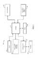
- FIG. 1illustrates a block diagram of a processor-based device having a memory that includes memory devices fabricated in accordance with embodiments of the present invention
- FIG. 2illustrates a block diagram of a memory device having a memory array fabricated in accordance with embodiments of the present invention
- FIG. 3is schematic diagram of a NAND flash memory array having memory cells fabricated in accordance with embodiments of the present invention
- FIG. 4is a cross-sectional view of a paired NAND string having even and odd blocks in accordance with embodiments of the present invention
- FIG. 5is a cross-sectional view of a paired NAND string having even and odd blocks that have inconsistent select gate to memory cell spacing in accordance with embodiments of the present invention.
- FIG. 6illustrates a technique for applying erase voltages to memory cells in accordance with embodiments of the present invention.
- FIG. 1a block diagram depicting a processor-based system, generally designated by reference numeral 10 , is illustrated.
- the system 10may be any of a variety of types such as a computer, pager, cellular phone, personal organizer, control circuit, etc.
- a processor 12such as a microprocessor, controls the processing of system functions and requests in the system 10 .
- the processor 12may comprise a plurality of processors that share system control.
- the system 10typically includes a power supply 14 .
- the power supply 14may advantageously include permanent batteries, replaceable batteries, and/or rechargeable batteries.
- the power supply 14may also include an AC adapter, so the system 10 may be plugged into a wall outlet, for instance.
- the power supply 14may also include a DC adapter such that the system 10 may be plugged into a vehicle cigarette lighter, for instance.
- a user interface 16may be coupled to the processor 12 .
- the user interface 16may include buttons, switches, a keyboard, a light pen, a mouse, and/or a voice recognition system, for instance.
- a display 18may also be coupled to the processor 12 .
- the display 18may include an LCD display, a CRT, LEDs, and/or an audio display, for example.
- an RF sub-system/baseband processor 20may also be coupled to the processor 12 .
- the RF sub-system/baseband processor 20may include an antenna that is coupled to an RF receiver and to an RF transmitter (not shown).
- a communications port 22may also be coupled to the processor 12 .
- the communications port 22may be adapted to be coupled to one or more peripheral devices 24 such as a modem, a printer, a computer, or to a network, such as a local area network, remote area network, intranet, or the Internet, for instance.
- the processor 12controls the functioning of the system 10 by implementing software programs, memory is used to enable the processor 12 to be efficient.
- the memoryis coupled to the processor 12 to store and facilitate execution of various programs.
- the processor 12may be coupled to system memory 26 , which may include volatile memory, such as Dynamic Random Access Memory (DRAM) and/or Static Random Access Memory (SRAM).
- the system memory 26may also include non-volatile memory, such as read-only memory (ROM), EEPROM, and/or flash memory to be used in conjunction with the volatile memory.
- the system memory 26may include one or more memory devices, such as flash memory devices, that may include a floating gate memory array fabricated in accordance with embodiments of the present invention.
- FIG. 2A block diagram illustrating a flash memory device 30 that may be included as a portion of the system memory 26 of FIG. 1 is illustrated in FIG. 2 .
- the flash memory device 30may be a NAND flash memory device.
- the flash memory device 30generally includes a memory array 32 .
- the memory array 32generally includes many rows and columns of conductive traces arranged in a grid pattern to form a number of memory cells.
- the sense lines that make up the memory array 32are generally referred to as “word lines”, rows or row lines.
- the “transfer lines”are generally referred to as “bit lines”, “digit lines”, columns or column lines
- the size of the memory array 32(i.e., the number of memory cells) will vary depending on the size of the flash memory device 30 .
- a row decoder block 34 and a column decoder block 36are provided and are configured to receive and translate address information from the processor 12 via the address bus 38 to access a particular memory cell in the memory array 32 .
- a sense amplifier block 40 having a plurality of the sense amplifiesis also provided between the column decoder 36 and the memory array 32 to sense and amplify individual values stored in the memory cells.
- a row driver block 42is provided between the row decoder block 34 and the memory array 32 to activate selected word lines in the memory array according to a given row address.
- the flash memory device 30may include a control circuit 48 configured to receive control signals from the processor 12 via the control bus 50 .
- the control circuit 48is coupled to each of the row decoder block 34 , the column decoder block 36 , the sense amplifier block 40 , the row driver block 42 and the data control circuit block 46 , and is generally configured to coordinate timing and control among the various circuits in the flash memory device 30 .
- the memory array 32comprises a NAND memory array 52 .
- the NAND memory array 52includes word lines WL( 0 )-WL(M) and intersecting local bit lines BL( 0 )-BL(M).
- the number of word lines WL and the number of bit lines BLare each a power of two (e.g., 256 word lines WL by 4,096 bit lines BL).
- the local bit lines BLare coupled to global bit lines (not shown) in a many-to-one relationship.
- the NAND memory array 52includes a floating gate transistor 54 located at each intersection of a word line WL and a local bit line BL.
- the floating gate transistors 54serve as non-volatile memory cells for storage of data in the NAND memory array 52 , as previously described.
- each floating gate transistorincludes a source, a drain, a floating gate, and a control gate.
- the control gate of each floating gate transistor 54is coupled to a respective word line WL.
- the floating gate transistors 54are connected in series, source to drain, to form a NAND string 56 formed between gate select lines. Specifically, the NAND strings 56 are formed between the drain select line GS(D) and the source select line GS(S).
- the drain select line GS(D)is coupled to each NAND string 56 through a respective drain select gate 58 .
- the source select line GS(S)is coupled to each NAND string 56 through a respective source select gate 60 .
- the drain select gates 58 and the source select gates 60may each comprise a field-effect transistor (FET), for instance.
- a column of the memory array 52includes a NAND string 56 and the source select gate 60 and drain select gate 58 connected thereto.
- a row of the floating gate transistors 52are those transistors commonly coupled to a given word line WL.
- each source select gate 60is connected to a common source line CSL.
- the drain of each source select gateis coupled to the source of a floating gate transistor 54 in a respective NAND string 56 .
- the gate of each source select gate 60is coupled to the source select line GS(S).
- each drain select gate 58is connected to a respective local bit line BL for the corresponding NAND string 56 .
- the source of each drain select gate 58is connected to the drain of a floating gate transistor 54 of a respective NAND string 56 . Accordingly, as illustrated in FIG. 3 , each NAND string 56 is coupled between a respective drain select gate 58 and source select gate 60 .
- the gate of each drain select gate 58is coupled to the drain select line GS(D).
- Differential voltages across the word linesalter the charge in the floating gates to program or erase the memory cells.
- a voltageis applied to the control gate while a program or inhibit voltage is applied to the bit lines.
- the voltage applied to the control gatemay be between 15 and 20 volts, for example.
- the substrateis raised to a high voltage, such as 20 volts, for example, while the word lines are coupled to ground or a low voltage, i.e. 1.5 volts or less.
- the source select and drain select gatesare left floating during the erase operation, so that electrons flow out of the floating gate and into the substrate.
- FIG. 4is a cross-sectional view of a paired NAND string 70 .
- Each floating gate transistor in the paired NAND string 70generally includes a gate dielectric 62 , such as silicon dioxide (SiO 2 ).
- Each floating gate transistoralso includes an isolated floating gate 64 , which may comprise polysilicon, for example.
- each floating gate transistoralso includes a control gate 66 , which may be formed of a single conductive layer, such as polysilicon.
- each of the floating gate transistors in a single word line WLmay share a common control gate 66 .
- the floating gates 64 and control gate 66are electrically isolated from one another by an inter-gate dielectric layer 68 .
- the inter-gate dielectric layer 68may comprise SiO 2 or SiN x , for example.
- the paired NAND string 70includes an even block 72 and an odd block 74 , each having source select gates 76 and 82 , respectively, and drain select gates 78 and 80 , respectively.
- the even and odd word lines WL( 0 )-WL(M)are located in between the select gates 76 and 78 in the even block 72 and select gates 80 and 82 in the odd block 74 .
- a program voltageis applied to the control gate 66 to program the memory cells, while an erase voltage is applied to the substrate 84 during an erase operation.
- the program and erase times for the memory cellsmay vary. In particular, the memory cells of the edge word lines may be slower during both the program and erase operations.
- FIG. 5illustrates a cross-sectional view of a paired NAND string 90 where such misalignment has occurred. Similar to the paired NAND string 70 of FIG. 4 , the paired NAND string 90 has both an even block 92 and an odd block 94 . The even block 92 has a source select gate 96 and a drain select gate 98 , and the odd block 94 has a drain select gate 100 and a source select gate 102 . The word lines are located in between the select gates 96 , 98 , 100 and 102 of the even and odd blocks 92 and 94 .
- the WL( 0 ) of the even blockwhich is referred to hereinafter as the “even WL( 0 )”
- the WL(M) of the even block(which is referred to hereinafter as the “even WL(M)”) is located a distance B from the even select gate 98 .
- the WL(M) of the odd blockwhich is referred to herinafter as the “odd WL(M)”
- the WL( 0 ) of the odd blockwhich is referred to hereinafter as the “odd WL( 0 )”
- the distances A and Care approximately equal and less than the distances B and D, which are also approximately equal. Because of the misalignment, the coupling ratio of the edge memory cells with the select gates is inconsistent between the even and odd NAND strings 92 and 94 , exacerbating an existing inconsistency in the program and erase times for the memory cells.
- the differential voltage between the memory cells and the substrate 84can vary across the memory cells of the NAND string 70 .
- the program voltage V pg of the even WL( 0 )may be set to be greater than the program voltage V pg of the even WL(M).
- the program voltage V pg for the odd WL(M)may be set to be greater than the program voltage V pg from the odd WL( 0 ). Additionally, the program voltage V pg for the even WL( 0 ) may be equal to or greater than the program voltage V pg of the odd WL(M), and the program voltage V pg for the odd WL( 0 ) may be greater than or equal to the program voltage V pg for the even WL(M).
- the relationship between the various program voltagesmay be: V pg for odd WL( 0 ) ⁇ V pg for even WL(M) >V pg even WL( 0 ) ⁇ V pg for odd WL(M).
- Providing the multiple program voltages levelsallows for word line specific adjustments to the program speeds of the memory cells to reduce the variability in program times of the memory cells.
- Various voltage levelsmay also be implemented for erase operations to reduce the variability in erase times of the memory cells.
- a high voltageis applied to the substrate and, generally, the control gate is coupled to a reference potential, such as ground.
- a reference potentialsuch as ground.
- erase voltagesmay be applied to the control gates.
- the application of different erase voltages to the control gatesadjusts the erase voltage threshold V t and helps to compensate for misalignment of the memory cells relative to the select gates.
- the voltages appliedmay range from approximately 0 volts to approximately 2.5 volts.
- the erase voltage applied to the even WL( 0 )may be zero volts
- the erase voltage applied to the even WL(M)may be 0.5 volts
- the erase voltage applied to even WL( 1 )-WL(M- 1 )may be 1.5 volts.
- the erase voltage level applied to the odd WL(M)may be approximately the same as that applied to the even WL( 0 ) (i.e., zero volts), while the erase voltage applied to the odd WL( 0 ) may be equal to the erase voltage applied to the even WL(M) (i.e., 0.5 volts).
- the erase voltage levels applied to the edge memory cells coupled to WL( 0 ) and WL (M)are less than the erase voltage levels applied to the other memory cells in the respective NAND block strings 92 and 94 .
- NAND memory arraysmay include a section of odd and even memory block strings that are configured to be used in the event of failure of a memory block strings that are currently in use.
- These redundant even and odd blocksmay be assigned to replace either even or odd blocks and, as a result, may be logically associated with a block that is physically different than the redundant block.
- a redundant even blockmay replace an odd block.
- the program and erase voltage levels for even blockswill be used, even though logically the memory cell may be associated or recognized as an odd block.
- a physical odd block used to replace a logical even blockwould use the program and erase voltages for a physical odd block, not an even block.
- the voltages implementedare consistent based on the physical characteristics of the blocks.
- FIG. 6a flow chart illustrating an exemplary technique for applying program and erase voltages to memory cells of a floating gate memory array is shown in FIG. 6 and generally referred to by the reference numeral 110 .
- the technique 110begins by determining whether the memory cells are misaligned, as indicated at block 112 . This determination may be performed in several ways. For example, in accordance with one technique, misalignment may be determined based on the relative program and erase times of the edge lines in the odd and even blocks.
- the sense amplifier block 40 of FIG. 2may be used to obtain information in this regard. Specifically, the sense amplifier block 40 may determine whether an erase or program operation has been successful for all the word lines in a block and whether the operation needs to be performed again for particular word line. This information can be used to determine whether the blocks are exhibiting signs characteristic of a misalignment. If it is determined that the memory cells are not misaligned, then standard voltages may be used, as indicated at block 114 .
- word line specific voltagesmay be determined to perform the program and erase operation, as indicated at block 116 .
- the determination of specific voltages for the program and erase operationsmay be determined based on the specific characteristics of the particular memory array or, alternatively, the voltages may be determined based on average effective erase and program voltages used in similar memory cells.
- the specific voltages for the program and erase operationsmay be set by applying an algorithm to the data retrieved by the sense amplifiers 40 that can adjust the program and erase voltages to optimal levels.
- the voltage levels for odd and even blocksmay be programmed in advance and once it is determined that the memory cells are misaligned, the programmed voltage levels are used.
- edge word lines WL( 0 ) and WL(M) in the even and odd blocksshould be correlated as set forth above.
- the even WL( 0 ) and the odd WL (M) erase voltagesmay be set equal to each other and the odd WL ( 0 ) and even WL (M) erase voltages may be set equal to each other.
- the program and erase voltagesare set, as indicated at block 118 , and the memory array may be used.
- the voltage levelsmay be determined again, as indicated by arrow 120 .
Landscapes
- Engineering & Computer Science (AREA)
- Microelectronics & Electronic Packaging (AREA)
- Read Only Memory (AREA)
- Non-Volatile Memory (AREA)
- Semiconductor Memories (AREA)
- General Engineering & Computer Science (AREA)
Abstract
Description
- This application is a continuation of U.S. application Ser. No. 13/118,198, filed on May 27, 2011, which is a divisional of U.S. application Ser. No. 11/951,171, filed on Dec. 5, 2007, which issued as U.S. Pat. No. 7,952,927 on May 31, 2011.
- 1. Field Of The Invention
- Embodiments of the present invention relate generally to memory devices and, more particularly, in one or more embodiments, to adjusting erase voltages in memory devices.
- 2. Description of The Related Art
- Processor-based systems, such as computers, typically include one or more memory devices to provide storage capability for the system. System memory is generally provided in the form of one or more integrated circuit chips or devices and generally includes both random access memory (RAM) and read-only memory (ROM). System RAM is typically large and volatile and provides the system's main memory. Static RAM and Dynamic RAM are commonly employed types of random access memory. In contrast, system ROM is generally small and includes non-volatile memory for storing initialization routines and identification information. Electrically-erasable read only memory (EEPROM) is one commonly employed type of memory, wherein an electrical charge may be used to program and/or erase data in the memory.
- One type of non-volatile memory that is of particular use is a flash memory. A flash memory is a type of EEPROM that can be erased and reprogrammed in blocks. Flash memory is often employed in personal computer systems in order to store the Basic Input Output System (BIOS) program such that it can be easily updated. Flash memory is also employed in wireless electronic devices, because it enables the manufacturer to support new communication protocols as they become standardized and provides the ability to remotely upgrade the device for enhanced features.
- Flash memory includes a memory array having a large number of memory cells arranged in “rows” and “columns”. The memory cells are generally grouped into pages which may be programmed simultaneously. Additionally, the pages are grouped into blocks and the cells within a block may all be erased simultaneously. Each of the memory cells includes a memory cell with a charge storage node, such as a floating-gate field-effect transistor capable of holding a charge. Other charge storage nodes could include, for example, charge trapping layers and the like. Floating gate memory cells differ from standard MOSFET designs in that they include an electrically isolated gate, referred to as the “floating gate,” in addition to the standard control gate. The floating gate is generally formed over the channel and separated from the channel by a gate oxide. The control gate is formed directly above the floating gate and is separated from the floating gate by another thin oxide layer. A floating gate memory cell stores information by holding electrical charge within the floating gate. By adding or removing charge from the floating gate, the threshold voltage of the cell changes, thereby defining whether this memory cell is programmed or erased.
- A NAND flash memory device is a common type of flash memory device, so called for the logical form in which the basic memory cell configuration is arranged. Typically, the array of memory cells for NAND flash memory devices is arranged such that the control gate of each memory cell of a row of the array is connected to a select line, which is often referred to as a word line. Columns of the array include strings (often termed NAND strings) of memory cells connected together in series, source to drain, between a pair of select lines, a source select line and a drain select line. The source select line includes a source select gate at each intersection between a NAND string and the source select line, and the drain select line includes a drain select gate at each intersection between a NAND string and the drain select line. The select gates are typically field-effect transistors. Each source select gate is connected to a source line, while each drain select gate is connected to a transfer line, which is often referred to as a bit line.
- The memory array is accessed by a row decoder activating a row of memory cells by selecting the word line connected to a control gate of a memory cell. In addition, the word lines connected to the control gates of unselected memory cells of each string are driven to operate the unselected memory cells of each string as pass transistors, so that they pass current in a manner that is unrestricted by their stored data values. Current then flows from the source line to the bit line through each NAND string via the corresponding select gates, restricted only by the selected memory cells of each string. This places the current-encoded data values of the row of selected memory cells on the bit lines.
- As mentioned above, memory cells may be programmed on a page basis and erased on a block basis. However, memory cells adjacent to the select gates (referred to as “edge memory cells”) have shown slower program and erase times than other memory cells. This is due in part to the edge cells having a low coupling ratio with the source or drain select gates to which they are adjacent and a higher coupling ratio with the substrate. Additionally, the coupling ratio of the edge memory cells with the select gates is inconsistent due to misalignment between the memory cells. The misalignment occurs during processes commonly used to manufacture the floating gate memory devices. Additionally, where blocks are manufactured in block pairs, i.e., even and odd blocks, the misalignment is generally different between the first block and the second block of the block pair. The variance in program and erase times caused by the misalignment of the memory cells is generally undesirable.
- Embodiments of the present invention may be directed to one or more of the problems set forth above.
FIG. 1 illustrates a block diagram of a processor-based device having a memory that includes memory devices fabricated in accordance with embodiments of the present invention;FIG. 2 illustrates a block diagram of a memory device having a memory array fabricated in accordance with embodiments of the present invention;FIG. 3 is schematic diagram of a NAND flash memory array having memory cells fabricated in accordance with embodiments of the present invention;FIG. 4 is a cross-sectional view of a paired NAND string having even and odd blocks in accordance with embodiments of the present invention;FIG. 5 is a cross-sectional view of a paired NAND string having even and odd blocks that have inconsistent select gate to memory cell spacing in accordance with embodiments of the present invention; andFIG. 6 illustrates a technique for applying erase voltages to memory cells in accordance with embodiments of the present invention.- Turning now to the drawings, and referring initially to
FIG. 1 , a block diagram depicting a processor-based system, generally designated byreference numeral 10, is illustrated. Thesystem 10 may be any of a variety of types such as a computer, pager, cellular phone, personal organizer, control circuit, etc. In a typical processor-based device, aprocessor 12, such as a microprocessor, controls the processing of system functions and requests in thesystem 10. Further, theprocessor 12 may comprise a plurality of processors that share system control. - The
system 10 typically includes apower supply 14. For instance, if thesystem 10 is a portable system, thepower supply 14 may advantageously include permanent batteries, replaceable batteries, and/or rechargeable batteries. Thepower supply 14 may also include an AC adapter, so thesystem 10 may be plugged into a wall outlet, for instance. Thepower supply 14 may also include a DC adapter such that thesystem 10 may be plugged into a vehicle cigarette lighter, for instance. - Various other devices may be coupled to the
processor 12 depending on the functions that thesystem 10 performs. For instance, auser interface 16 may be coupled to theprocessor 12. Theuser interface 16 may include buttons, switches, a keyboard, a light pen, a mouse, and/or a voice recognition system, for instance. Adisplay 18 may also be coupled to theprocessor 12. Thedisplay 18 may include an LCD display, a CRT, LEDs, and/or an audio display, for example. - Furthermore, an RF sub-system/
baseband processor 20 may also be coupled to theprocessor 12. The RF sub-system/baseband processor 20 may include an antenna that is coupled to an RF receiver and to an RF transmitter (not shown). Acommunications port 22 may also be coupled to theprocessor 12. Thecommunications port 22 may be adapted to be coupled to one or moreperipheral devices 24 such as a modem, a printer, a computer, or to a network, such as a local area network, remote area network, intranet, or the Internet, for instance. - Because the
processor 12 controls the functioning of thesystem 10 by implementing software programs, memory is used to enable theprocessor 12 to be efficient. Generally, the memory is coupled to theprocessor 12 to store and facilitate execution of various programs. For instance, theprocessor 12 may be coupled tosystem memory 26, which may include volatile memory, such as Dynamic Random Access Memory (DRAM) and/or Static Random Access Memory (SRAM). Thesystem memory 26 may also include non-volatile memory, such as read-only memory (ROM), EEPROM, and/or flash memory to be used in conjunction with the volatile memory. As described further below, thesystem memory 26 may include one or more memory devices, such as flash memory devices, that may include a floating gate memory array fabricated in accordance with embodiments of the present invention. - A block diagram illustrating a
flash memory device 30 that may be included as a portion of thesystem memory 26 ofFIG. 1 is illustrated inFIG. 2 . As will be described further below with respect toFIG. 3 , theflash memory device 30 may be a NAND flash memory device. Theflash memory device 30 generally includes amemory array 32. Thememory array 32 generally includes many rows and columns of conductive traces arranged in a grid pattern to form a number of memory cells. The sense lines that make up thememory array 32 are generally referred to as “word lines”, rows or row lines. The “transfer lines” are generally referred to as “bit lines”, “digit lines”, columns or column lines The size of the memory array32 (i.e., the number of memory cells) will vary depending on the size of theflash memory device 30. - To access the
memory array 32, arow decoder block 34 and acolumn decoder block 36 are provided and are configured to receive and translate address information from theprocessor 12 via theaddress bus 38 to access a particular memory cell in thememory array 32. Asense amplifier block 40 having a plurality of the sense amplifies is also provided between thecolumn decoder 36 and thememory array 32 to sense and amplify individual values stored in the memory cells. Further, arow driver block 42 is provided between therow decoder block 34 and thememory array 32 to activate selected word lines in the memory array according to a given row address. - During read and write operations, data may be transferred to and from the
flash memory device 30 via thedata bus 44. The coordination of the data and address information may be conducted through a datacontrol circuit block 46. Finally, theflash memory device 30 may include acontrol circuit 48 configured to receive control signals from theprocessor 12 via thecontrol bus 50. Thecontrol circuit 48 is coupled to each of therow decoder block 34, thecolumn decoder block 36, thesense amplifier block 40, therow driver block 42 and the datacontrol circuit block 46, and is generally configured to coordinate timing and control among the various circuits in theflash memory device 30. - An embodiment of the
memory array 32 ofFIG. 2 is illustrated inFIG. 3 . In the present embodiment, thememory array 32 comprises aNAND memory array 52. TheNAND memory array 52 includes word lines WL(0)-WL(M) and intersecting local bit lines BL(0)-BL(M). As will be appreciated, for ease of addressing in the digital environment, the number of word lines WL and the number of bit lines BL are each a power of two (e.g., 256 word lines WL by 4,096 bit lines BL). The local bit lines BL are coupled to global bit lines (not shown) in a many-to-one relationship. - The
NAND memory array 52 includes a floatinggate transistor 54 located at each intersection of a word line WL and a local bit line BL. The floatinggate transistors 54 serve as non-volatile memory cells for storage of data in theNAND memory array 52, as previously described. As will be appreciated, each floating gate transistor includes a source, a drain, a floating gate, and a control gate. The control gate of each floatinggate transistor 54 is coupled to a respective word line WL. The floatinggate transistors 54 are connected in series, source to drain, to form aNAND string 56 formed between gate select lines. Specifically, the NAND strings56 are formed between the drain select line GS(D) and the source select line GS(S). The drain select line GS(D) is coupled to eachNAND string 56 through a respective drainselect gate 58. Similarly, the source select line GS(S) is coupled to eachNAND string 56 through a respective sourceselect gate 60. The drainselect gates 58 and the sourceselect gates 60 may each comprise a field-effect transistor (FET), for instance. A column of thememory array 52 includes aNAND string 56 and the sourceselect gate 60 and drainselect gate 58 connected thereto. A row of the floatinggate transistors 52 are those transistors commonly coupled to a given word line WL. - The source of each source
select gate 60 is connected to a common source line CSL. The drain of each source select gate is coupled to the source of a floatinggate transistor 54 in arespective NAND string 56. The gate of each sourceselect gate 60 is coupled to the source select line GS(S). - The drain of each drain
select gate 58 is connected to a respective local bit line BL for thecorresponding NAND string 56. The source of each drainselect gate 58 is connected to the drain of a floatinggate transistor 54 of arespective NAND string 56. Accordingly, as illustrated inFIG. 3 , eachNAND string 56 is coupled between a respective drainselect gate 58 and sourceselect gate 60. The gate of each drainselect gate 58 is coupled to the drain select line GS(D). - Differential voltages across the word lines alter the charge in the floating gates to program or erase the memory cells. Specifically, in programming the memory cells, a voltage is applied to the control gate while a program or inhibit voltage is applied to the bit lines. The voltage applied to the control gate may be between 15 and 20 volts, for example. Alternatively, during an erase operation the substrate is raised to a high voltage, such as 20 volts, for example, while the word lines are coupled to ground or a low voltage, i.e. 1.5 volts or less. The source select and drain select gates are left floating during the erase operation, so that electrons flow out of the floating gate and into the substrate.
- As mentioned above, the edge memory cells (i.e., the memory cells adjacent to the select gates) have shown slower program and erase times than other memory cells in a typical memory array due in part to the edge cells having a low coupling ratio with the select gates and a higher coupling ratio with the substrate tub.
FIG. 4 is a cross-sectional view of a pairedNAND string 70. Each floating gate transistor in the pairedNAND string 70 generally includes agate dielectric 62, such as silicon dioxide (SiO2). Each floating gate transistor also includes an isolated floatinggate 64, which may comprise polysilicon, for example. As previously discussed, each floating gate transistor also includes acontrol gate 66, which may be formed of a single conductive layer, such as polysilicon. Because of the configuration and operation of the memory array, each of the floating gate transistors in a single word line WL may share acommon control gate 66. The floatinggates 64 andcontrol gate 66 are electrically isolated from one another by an inter-gatedielectric layer 68. The inter-gatedielectric layer 68 may comprise SiO2or SiNx, for example. - The paired
NAND string 70 includes aneven block 72 and anodd block 74, each having source selectgates 76 and82, respectively, and drainselect gates 78 and80, respectively. The even and odd word lines WL(0)-WL(M) are located in between theselect gates odd block 74. As discussed above, a program voltage is applied to thecontrol gate 66 to program the memory cells, while an erase voltage is applied to thesubstrate 84 during an erase operation. However, the program and erase times for the memory cells may vary. In particular, the memory cells of the edge word lines may be slower during both the program and erase operations. - The slower program and erase of edge word lines may be due, in part, to misalignment of the edge word lines with respect to select gates during the manufacturing processes.
FIG. 5 illustrates a cross-sectional view of a paired NAND string90 where such misalignment has occurred. Similar to the pairedNAND string 70 ofFIG. 4 , the paired NAND string90 has both aneven block 92 and anodd block 94. Theeven block 92 has a sourceselect gate 96 and a drainselect gate 98, and theodd block 94 has a drainselect gate 100 and a sourceselect gate 102. The word lines are located in between theselect gates odd blocks - As illustrated in
FIG. 5 , the WL(0) of the even block, which is referred to hereinafter as the “even WL(0)”, has been misaligned so that it is located a distance A from the sourceselect gate 96, while the WL(M) of the even block (which is referred to hereinafter as the “even WL(M)”) is located a distance B from the evenselect gate 98. Similarly, the WL(M) of the odd block, which is referred to herinafter as the “odd WL(M)”, has been misaligned relative to the drainselect gate 100 so that they are a distance C apart and the WL(0) of the odd block, which is referred to hereinafter as the “odd WL(0)”, is located a distance D from the sourceselect gate 102. In this example, the distances A and C are approximately equal and less than the distances B and D, which are also approximately equal. Because of the misalignment, the coupling ratio of the edge memory cells with the select gates is inconsistent between the even and odd NAND strings92 and94, exacerbating an existing inconsistency in the program and erase times for the memory cells. - In order to compensate for the slower program and erase times of the edge word lines, different voltage levels may be applied to adjust an erase voltage threshold Vtfor memory cells of edge word lines. Thus, the differential voltage between the memory cells and the
substrate 84 can vary across the memory cells of theNAND string 70. In the case of a program operation where the distance A between the even WL(0) and the sourceselect gate 96 is less than the distance B between the even WL(M) and the drainselect gate 98, the program voltage Vpgof the even WL(0) may be set to be greater than the program voltage Vpgof the even WL(M). Similarly, the program voltage Vpgfor the odd WL(M) may be set to be greater than the program voltage Vpgfrom the odd WL(0). Additionally, the program voltage Vpgfor the even WL(0) may be equal to or greater than the program voltage Vpgof the odd WL(M), and the program voltage Vpgfor the odd WL(0) may be greater than or equal to the program voltage Vpgfor the even WL(M). - Thus, the following relationship is established for the respective program voltages when the distance A is less than the distance B: Vpgfor even WL(0) ≧Vpgfor odd WL(M) >Vpgfor odd WL(0) ≧Vpgfor even WL(M). In the event that the even WL(0) is closer to the source
select gate 96 than the even WL(M) is to the drainselect gate 98, the respective voltage may be: Vpgfor even WL(0)=16.8; Vpgfor odd WL(M)=16.6; Vpgfor even WL(M) 16.0; Vpgfor odd WL(0)=16.2. Alternatively, if the distance A is greater than the distance B, the relationship between the various program voltages may be: Vpgfor odd WL(0) ≧Vpgfor even WL(M) >Vpgeven WL(0) ≧Vpgfor odd WL(M). - Providing the multiple program voltages levels allows for word line specific adjustments to the program speeds of the memory cells to reduce the variability in program times of the memory cells. Various voltage levels may also be implemented for erase operations to reduce the variability in erase times of the memory cells.
- As mentioned above, during an erase operation, a high voltage is applied to the substrate and, generally, the control gate is coupled to a reference potential, such as ground. However, in order to provide more consistent erase times for memory cells within a block, erase voltages may be applied to the control gates. The application of different erase voltages to the control gates adjusts the erase voltage threshold Vtand helps to compensate for misalignment of the memory cells relative to the select gates. The voltages applied may range from approximately 0 volts to approximately 2.5 volts. For example, for erasure of the memory cells of the
even NAND string 92, when the distance A is less than the distance B, the erase voltage applied to the even WL(0) may be zero volts, the erase voltage applied to the even WL(M) may be 0.5 volts, and the erase voltage applied to even WL(1)-WL(M-1) may be 1.5 volts. Because the distance C is approximately equal to the distance A, the erase voltage level applied to the odd WL(M) may be approximately the same as that applied to the even WL(0) (i.e., zero volts), while the erase voltage applied to the odd WL(0) may be equal to the erase voltage applied to the even WL(M) (i.e., 0.5 volts). In both the even and odd block strings92 and94, the erase voltage levels applied to the edge memory cells coupled to WL(0) and WL (M) are less than the erase voltage levels applied to the other memory cells in the respective NAND block strings92 and94. - In implementing the different program and erase voltages for the edge word lines, the voltage levels should be determined based on the physical characteristics of the blocks and not logical associations with other memory cell. In particular, NAND memory arrays may include a section of odd and even memory block strings that are configured to be used in the event of failure of a memory block strings that are currently in use. These redundant even and odd blocks may be assigned to replace either even or odd blocks and, as a result, may be logically associated with a block that is physically different than the redundant block. Specifically, for example, a redundant even block may replace an odd block. Where the redundant even block is being used to replace an odd block, the program and erase voltage levels for even blocks will be used, even though logically the memory cell may be associated or recognized as an odd block. Similarly, a physical odd block used to replace a logical even block would use the program and erase voltages for a physical odd block, not an even block. Thus, the voltages implemented are consistent based on the physical characteristics of the blocks.
- In view of the foregoing, a flow chart illustrating an exemplary technique for applying program and erase voltages to memory cells of a floating gate memory array is shown in
FIG. 6 and generally referred to by thereference numeral 110. Thetechnique 110 begins by determining whether the memory cells are misaligned, as indicated atblock 112. This determination may be performed in several ways. For example, in accordance with one technique, misalignment may be determined based on the relative program and erase times of the edge lines in the odd and even blocks. Specifically, if the even word line WL(0) is erasing approximately as fast as the odd word line WL(M) and both are erasing faster than the even word line WL(M) and the odd word line WL(0), then it may indicate that there is a misalignment. Thesense amplifier block 40 ofFIG. 2 may be used to obtain information in this regard. Specifically, thesense amplifier block 40 may determine whether an erase or program operation has been successful for all the word lines in a block and whether the operation needs to be performed again for particular word line. This information can be used to determine whether the blocks are exhibiting signs characteristic of a misalignment. If it is determined that the memory cells are not misaligned, then standard voltages may be used, as indicated atblock 114. - Alternatively, however, if it is determined that the memory cells are misaligned, word line specific voltages may be determined to perform the program and erase operation, as indicated at
block 116. The determination of specific voltages for the program and erase operations may be determined based on the specific characteristics of the particular memory array or, alternatively, the voltages may be determined based on average effective erase and program voltages used in similar memory cells. For example, the specific voltages for the program and erase operations may be set by applying an algorithm to the data retrieved by thesense amplifiers 40 that can adjust the program and erase voltages to optimal levels. Alternatively, the voltage levels for odd and even blocks may be programmed in advance and once it is determined that the memory cells are misaligned, the programmed voltage levels are used. Regardless, in setting the program and erase voltages, edge word lines WL(0) and WL(M) in the even and odd blocks should be correlated as set forth above. For example, for the erase operation, the even WL(0) and the odd WL (M) erase voltages may be set equal to each other and the odd WL (0) and even WL (M) erase voltages may be set equal to each other. - After the appropriate voltage levels have been determined, the program and erase voltages are set, as indicated at
block 118, and the memory array may be used. In accordance with one embodiment, if the edge word lines WL(0) and WL(M) continue to exhibit slower program and erase times, the voltage levels may be determined again, as indicated byarrow 120. - While embodiments of the invention may be susceptible to various modifications and alternative forms, specific embodiments have been shown by way of example in the drawings and have been described in detail herein. However, it should be understood that the invention is not intended to be limited to the particular forms disclosed. Rather, embodiments of the invention are to cover all modifications, equivalents, and alternatives falling within the spirit and scope of these embodiments, as defined by the following appended claims.
Claims (23)
Priority Applications (1)
| Application Number | Priority Date | Filing Date | Title |
|---|---|---|---|
| US14/150,568US9030874B2 (en) | 2007-12-05 | 2014-01-08 | Adjusting program and erase voltages in a memory device |
Applications Claiming Priority (3)
| Application Number | Priority Date | Filing Date | Title |
|---|---|---|---|
| US11/951,171US7952927B2 (en) | 2007-12-05 | 2007-12-05 | Adjusting program and erase voltages in a memory device |
| US13/118,198US8634244B2 (en) | 2007-12-05 | 2011-05-27 | Adjusting program and erase voltages in a memory device |
| US14/150,568US9030874B2 (en) | 2007-12-05 | 2014-01-08 | Adjusting program and erase voltages in a memory device |
Related Parent Applications (1)
| Application Number | Title | Priority Date | Filing Date |
|---|---|---|---|
| US13/118,198ContinuationUS8634244B2 (en) | 2007-12-05 | 2011-05-27 | Adjusting program and erase voltages in a memory device |
Publications (2)
| Publication Number | Publication Date |
|---|---|
| US20140119121A1true US20140119121A1 (en) | 2014-05-01 |
| US9030874B2 US9030874B2 (en) | 2015-05-12 |
Family
ID=40721512
Family Applications (3)
| Application Number | Title | Priority Date | Filing Date |
|---|---|---|---|
| US11/951,171Active2029-02-13US7952927B2 (en) | 2007-12-05 | 2007-12-05 | Adjusting program and erase voltages in a memory device |
| US13/118,198Active2028-09-02US8634244B2 (en) | 2007-12-05 | 2011-05-27 | Adjusting program and erase voltages in a memory device |
| US14/150,568ActiveUS9030874B2 (en) | 2007-12-05 | 2014-01-08 | Adjusting program and erase voltages in a memory device |
Family Applications Before (2)
| Application Number | Title | Priority Date | Filing Date |
|---|---|---|---|
| US11/951,171Active2029-02-13US7952927B2 (en) | 2007-12-05 | 2007-12-05 | Adjusting program and erase voltages in a memory device |
| US13/118,198Active2028-09-02US8634244B2 (en) | 2007-12-05 | 2011-05-27 | Adjusting program and erase voltages in a memory device |
Country Status (1)
| Country | Link |
|---|---|
| US (3) | US7952927B2 (en) |
Cited By (7)
| Publication number | Priority date | Publication date | Assignee | Title |
|---|---|---|---|---|
| US9343171B1 (en) | 2015-02-09 | 2016-05-17 | Sandisk Technologies Inc. | Reduced erase-verify voltage for first-programmed word line in a memory device |
| US9704579B1 (en) | 2016-03-24 | 2017-07-11 | Powerchip Technology Corporation | Non-valatile semiconductor memory device and location based erasure methods |
| US9830963B1 (en) | 2016-05-24 | 2017-11-28 | Sandisk Technologies Llc | Word line-dependent and temperature-dependent erase depth |
| WO2017213717A1 (en)* | 2016-06-10 | 2017-12-14 | Cypress Semiconductor Corporation | Methods and devices for reducing program disturb in non-volatile memory cell arrays |
| US9984760B1 (en) | 2017-01-11 | 2018-05-29 | Sandisk Technologies Llc | Suppressing disturb of select gate transistors during erase in memory |
| US9997253B1 (en) | 2016-12-08 | 2018-06-12 | Cypress Semiconductor Corporation | Non-volatile memory array with memory gate line and source line scrambling |
| US10741253B1 (en) | 2019-02-20 | 2020-08-11 | Sandisk Technologies Llc | Memory device with compensation for erase speed variations due to blocking oxide layer thinning |
Families Citing this family (10)
| Publication number | Priority date | Publication date | Assignee | Title |
|---|---|---|---|---|
| US7952927B2 (en)* | 2007-12-05 | 2011-05-31 | Micron Technology, Inc. | Adjusting program and erase voltages in a memory device |
| US8874825B2 (en) | 2009-06-30 | 2014-10-28 | Sandisk Technologies Inc. | Storage device and method using parameters based on physical memory block location |
| KR102348094B1 (en)* | 2015-09-17 | 2022-01-07 | 에스케이하이닉스 주식회사 | Semiconductor memory device and operating method thereof |
| KR102379167B1 (en)* | 2015-10-26 | 2022-03-25 | 삼성전자주식회사 | Semiconductor device having register sets and data processing device including the same |
| US10147734B1 (en) | 2017-08-30 | 2018-12-04 | Cypress Semiconductor Corporation | Memory gate driver technology for flash memory cells |
| US10482985B2 (en) | 2018-02-05 | 2019-11-19 | Sandisk Technologies Llc | Dynamic erase loop dependent bias voltage |
| US10964398B2 (en) | 2018-09-28 | 2021-03-30 | Samsung Electronics Co., Ltd. | Memory device and a storage system using the same |
| KR102701788B1 (en)* | 2018-09-28 | 2024-08-30 | 삼성전자주식회사 | A memory device and a storage system using the same |
| US10748627B2 (en)* | 2018-12-21 | 2020-08-18 | Sandisk Technologies Llc | Reducing neighbor word line interference in a two-tier memory device by modifying word line programming order |
| CN111951853B (en)* | 2019-05-14 | 2023-05-05 | 兆易创新科技集团股份有限公司 | Method and device for controlling erasing operation and Nand flash memory |
Citations (6)
| Publication number | Priority date | Publication date | Assignee | Title |
|---|---|---|---|---|
| US7310280B2 (en)* | 2004-12-27 | 2007-12-18 | Hynix Semiconductor Inc | Flash memory device |
| US7539061B2 (en)* | 2006-05-10 | 2009-05-26 | Hynix Semiconductor Inc. | Method of programming flash memory device |
| US7663918B2 (en)* | 2005-01-12 | 2010-02-16 | Hynix Semiconductor Inc. | Nonvolatile memory device and method of programming/reading the same |
| US7688634B2 (en)* | 2007-08-06 | 2010-03-30 | Qimonda Ag | Method of operating an integrated circuit having at least one memory cell |
| US7952927B2 (en)* | 2007-12-05 | 2011-05-31 | Micron Technology, Inc. | Adjusting program and erase voltages in a memory device |
| US8045372B2 (en)* | 2007-04-06 | 2011-10-25 | Hynix Semiconductor Inc. | Flash memory device and method of operating the same |
Family Cites Families (6)
| Publication number | Priority date | Publication date | Assignee | Title |
|---|---|---|---|---|
| US6850441B2 (en)* | 2002-01-18 | 2005-02-01 | Sandisk Corporation | Noise reduction technique for transistors and small devices utilizing an episodic agitation |
| JP4245437B2 (en)* | 2003-08-08 | 2009-03-25 | シャープ株式会社 | Writing method for nonvolatile semiconductor memory device |
| KR100609568B1 (en)* | 2004-07-15 | 2006-08-08 | 에스티마이크로일렉트로닉스 엔.브이. | Page buffer of nonvolatile memory device, program method and read method using same |
| US7391654B2 (en)* | 2005-05-11 | 2008-06-24 | Micron Technology, Inc. | Memory block erasing in a flash memory device |
| US7212447B2 (en)* | 2005-08-04 | 2007-05-01 | Micron Technology, Inc. | NAND flash memory cell programming |
| US7936604B2 (en)* | 2005-08-30 | 2011-05-03 | Halo Lsi Inc. | High speed operation method for twin MONOS metal bit array |
- 2007
- 2007-12-05USUS11/951,171patent/US7952927B2/enactiveActive
- 2011
- 2011-05-27USUS13/118,198patent/US8634244B2/enactiveActive
- 2014
- 2014-01-08USUS14/150,568patent/US9030874B2/enactiveActive
Patent Citations (7)
| Publication number | Priority date | Publication date | Assignee | Title |
|---|---|---|---|---|
| US7310280B2 (en)* | 2004-12-27 | 2007-12-18 | Hynix Semiconductor Inc | Flash memory device |
| US7663918B2 (en)* | 2005-01-12 | 2010-02-16 | Hynix Semiconductor Inc. | Nonvolatile memory device and method of programming/reading the same |
| US7539061B2 (en)* | 2006-05-10 | 2009-05-26 | Hynix Semiconductor Inc. | Method of programming flash memory device |
| US8045372B2 (en)* | 2007-04-06 | 2011-10-25 | Hynix Semiconductor Inc. | Flash memory device and method of operating the same |
| US7688634B2 (en)* | 2007-08-06 | 2010-03-30 | Qimonda Ag | Method of operating an integrated circuit having at least one memory cell |
| US7952927B2 (en)* | 2007-12-05 | 2011-05-31 | Micron Technology, Inc. | Adjusting program and erase voltages in a memory device |
| US8634244B2 (en)* | 2007-12-05 | 2014-01-21 | Micron Technology, Inc. | Adjusting program and erase voltages in a memory device |
Cited By (15)
| Publication number | Priority date | Publication date | Assignee | Title |
|---|---|---|---|---|
| US9343171B1 (en) | 2015-02-09 | 2016-05-17 | Sandisk Technologies Inc. | Reduced erase-verify voltage for first-programmed word line in a memory device |
| US9704579B1 (en) | 2016-03-24 | 2017-07-11 | Powerchip Technology Corporation | Non-valatile semiconductor memory device and location based erasure methods |
| US9830963B1 (en) | 2016-05-24 | 2017-11-28 | Sandisk Technologies Llc | Word line-dependent and temperature-dependent erase depth |
| US10074438B2 (en) | 2016-06-10 | 2018-09-11 | Cypress Semiconductor Corporation | Methods and devices for reducing program disturb in non-volatile memory cell arrays |
| WO2017213717A1 (en)* | 2016-06-10 | 2017-12-14 | Cypress Semiconductor Corporation | Methods and devices for reducing program disturb in non-volatile memory cell arrays |
| US10446245B2 (en) | 2016-12-08 | 2019-10-15 | Cypress Semiconductor Corporation | Non-volatile memory array with memory gate line and source line scrambling |
| US9997253B1 (en) | 2016-12-08 | 2018-06-12 | Cypress Semiconductor Corporation | Non-volatile memory array with memory gate line and source line scrambling |
| US10192627B2 (en) | 2016-12-08 | 2019-01-29 | Cypress Semiconductor Corporation | Non-volatile memory array with memory gate line and source line scrambling |
| WO2018132186A1 (en)* | 2017-01-11 | 2018-07-19 | Sandisk Technologies Llc | Suppressing disturb of select gate transistors during erase in memory |
| US9984760B1 (en) | 2017-01-11 | 2018-05-29 | Sandisk Technologies Llc | Suppressing disturb of select gate transistors during erase in memory |
| EP3568856B1 (en)* | 2017-01-11 | 2021-07-21 | SanDisk Technologies LLC | Suppressing disturb of select gate transistors during erase in memory |
| US10741253B1 (en) | 2019-02-20 | 2020-08-11 | Sandisk Technologies Llc | Memory device with compensation for erase speed variations due to blocking oxide layer thinning |
| WO2020171871A1 (en)* | 2019-02-20 | 2020-08-27 | Sandisk Technologies Llc | Memory device with compensation for erase speed variations due to blocking oxide layer thinning |
| US10923197B2 (en) | 2019-02-20 | 2021-02-16 | Sandisk Technologies Llc | Memory device with compensation for erase speed variations due to blocking oxide layer thinning |
| CN113168865A (en)* | 2019-02-20 | 2021-07-23 | 桑迪士克科技有限责任公司 | Memory devices that compensate for changes in erase speed due to thinning of the blocking oxide layer |
Also Published As
| Publication number | Publication date |
|---|---|
| US20110228607A1 (en) | 2011-09-22 |
| US9030874B2 (en) | 2015-05-12 |
| US7952927B2 (en) | 2011-05-31 |
| US8634244B2 (en) | 2014-01-21 |
| US20090147582A1 (en) | 2009-06-11 |
Similar Documents
| Publication | Publication Date | Title |
|---|---|---|
| US9030874B2 (en) | Adjusting program and erase voltages in a memory device | |
| CN106169304B (en) | The method of erasing and refresh of non-volatile memory part | |
| US6370062B2 (en) | NAND-type flash memory device and method of operating the same | |
| US8194470B2 (en) | Methods of forming flash device with shared word lines | |
| US7773429B2 (en) | Non-volatile memory device and driving method thereof | |
| KR101692520B1 (en) | Nonvolatile memory device, operating method thereof and memory system including the same | |
| US7821834B2 (en) | Nonvolatile memory devices that utilize dummy memory cells to improve data reliability in charge trap memory arrays | |
| US7952936B2 (en) | Program-verify method | |
| US20140098611A1 (en) | Biasing system and method | |
| US20070133305A1 (en) | Method of erasing data with improving reliability in a nonvolatile semiconductor memory device | |
| KR100635924B1 (en) | How flash memory devices work | |
| JPH1187658A (en) | Memory cell and nonvolatile semiconductor memory device including the same | |
| US8634252B2 (en) | Methods of operating a memory device having a buried boosting plate | |
| US20160104538A1 (en) | Semiconductor device | |
| KR100379553B1 (en) | A array of flash memory cell and method for programming of data thereby and method for erased of data thereby | |
| KR20090000319A (en) | Nonvolatile Memory Device and Its Operation Method | |
| US20090003065A1 (en) | Flash cell with improved program disturb | |
| US9281073B2 (en) | Methods of operating a memory device having a buried boosting plate | |
| US20160247908A1 (en) | Nonvolatile semiconductor memory device | |
| US7675778B2 (en) | Memory devices having reduced word line current and method of operating and manufacturing the same | |
| KR100854871B1 (en) | Nonvolatile Memory Device and Program Method Using the Same | |
| CN108735266B (en) | Nonvolatile memory device with word erase and write disturb reduction | |
| KR20100034878A (en) | Non-volatile memory device | |
| JP2001015615A (en) | Nonvolatile semiconductor memory device |
Legal Events
| Date | Code | Title | Description |
|---|---|---|---|
| FEPP | Fee payment procedure | Free format text:PAYOR NUMBER ASSIGNED (ORIGINAL EVENT CODE: ASPN); ENTITY STATUS OF PATENT OWNER: LARGE ENTITY | |
| STCF | Information on status: patent grant | Free format text:PATENTED CASE | |
| AS | Assignment | Owner name:U.S. BANK NATIONAL ASSOCIATION, AS COLLATERAL AGENT, CALIFORNIA Free format text:SECURITY INTEREST;ASSIGNOR:MICRON TECHNOLOGY, INC.;REEL/FRAME:038669/0001 Effective date:20160426 Owner name:U.S. BANK NATIONAL ASSOCIATION, AS COLLATERAL AGEN Free format text:SECURITY INTEREST;ASSIGNOR:MICRON TECHNOLOGY, INC.;REEL/FRAME:038669/0001 Effective date:20160426 | |
| AS | Assignment | Owner name:MORGAN STANLEY SENIOR FUNDING, INC., AS COLLATERAL AGENT, MARYLAND Free format text:PATENT SECURITY AGREEMENT;ASSIGNOR:MICRON TECHNOLOGY, INC.;REEL/FRAME:038954/0001 Effective date:20160426 Owner name:MORGAN STANLEY SENIOR FUNDING, INC., AS COLLATERAL Free format text:PATENT SECURITY AGREEMENT;ASSIGNOR:MICRON TECHNOLOGY, INC.;REEL/FRAME:038954/0001 Effective date:20160426 | |
| AS | Assignment | Owner name:U.S. BANK NATIONAL ASSOCIATION, AS COLLATERAL AGENT, CALIFORNIA Free format text:CORRECTIVE ASSIGNMENT TO CORRECT THE REPLACE ERRONEOUSLY FILED PATENT #7358718 WITH THE CORRECT PATENT #7358178 PREVIOUSLY RECORDED ON REEL 038669 FRAME 0001. ASSIGNOR(S) HEREBY CONFIRMS THE SECURITY INTEREST;ASSIGNOR:MICRON TECHNOLOGY, INC.;REEL/FRAME:043079/0001 Effective date:20160426 Owner name:U.S. BANK NATIONAL ASSOCIATION, AS COLLATERAL AGEN Free format text:CORRECTIVE ASSIGNMENT TO CORRECT THE REPLACE ERRONEOUSLY FILED PATENT #7358718 WITH THE CORRECT PATENT #7358178 PREVIOUSLY RECORDED ON REEL 038669 FRAME 0001. ASSIGNOR(S) HEREBY CONFIRMS THE SECURITY INTEREST;ASSIGNOR:MICRON TECHNOLOGY, INC.;REEL/FRAME:043079/0001 Effective date:20160426 | |
| AS | Assignment | Owner name:JPMORGAN CHASE BANK, N.A., AS COLLATERAL AGENT, ILLINOIS Free format text:SECURITY INTEREST;ASSIGNORS:MICRON TECHNOLOGY, INC.;MICRON SEMICONDUCTOR PRODUCTS, INC.;REEL/FRAME:047540/0001 Effective date:20180703 Owner name:JPMORGAN CHASE BANK, N.A., AS COLLATERAL AGENT, IL Free format text:SECURITY INTEREST;ASSIGNORS:MICRON TECHNOLOGY, INC.;MICRON SEMICONDUCTOR PRODUCTS, INC.;REEL/FRAME:047540/0001 Effective date:20180703 | |
| AS | Assignment | Owner name:MICRON TECHNOLOGY, INC., IDAHO Free format text:RELEASE BY SECURED PARTY;ASSIGNOR:U.S. BANK NATIONAL ASSOCIATION, AS COLLATERAL AGENT;REEL/FRAME:047243/0001 Effective date:20180629 | |
| MAFP | Maintenance fee payment | Free format text:PAYMENT OF MAINTENANCE FEE, 4TH YEAR, LARGE ENTITY (ORIGINAL EVENT CODE: M1551); ENTITY STATUS OF PATENT OWNER: LARGE ENTITY Year of fee payment:4 | |
| AS | Assignment | Owner name:MICRON TECHNOLOGY, INC., IDAHO Free format text:RELEASE BY SECURED PARTY;ASSIGNOR:MORGAN STANLEY SENIOR FUNDING, INC., AS COLLATERAL AGENT;REEL/FRAME:050937/0001 Effective date:20190731 | |
| AS | Assignment | Owner name:MICRON TECHNOLOGY, INC., IDAHO Free format text:RELEASE BY SECURED PARTY;ASSIGNOR:JPMORGAN CHASE BANK, N.A., AS COLLATERAL AGENT;REEL/FRAME:051028/0001 Effective date:20190731 Owner name:MICRON SEMICONDUCTOR PRODUCTS, INC., IDAHO Free format text:RELEASE BY SECURED PARTY;ASSIGNOR:JPMORGAN CHASE BANK, N.A., AS COLLATERAL AGENT;REEL/FRAME:051028/0001 Effective date:20190731 | |
| MAFP | Maintenance fee payment | Free format text:PAYMENT OF MAINTENANCE FEE, 8TH YEAR, LARGE ENTITY (ORIGINAL EVENT CODE: M1552); ENTITY STATUS OF PATENT OWNER: LARGE ENTITY Year of fee payment:8 |