US20140097546A1 - Multi-function and shielded 3d interconnects - Google Patents
Multi-function and shielded 3d interconnectsDownload PDFInfo
- Publication number
- US20140097546A1 US20140097546A1US14/104,407US201314104407AUS2014097546A1US 20140097546 A1US20140097546 A1US 20140097546A1US 201314104407 AUS201314104407 AUS 201314104407AUS 2014097546 A1US2014097546 A1US 2014097546A1
- Authority
- US
- United States
- Prior art keywords
- conductive
- opening
- conductive element
- forming
- dielectric layer
- Prior art date
- Legal status (The legal status is an assumption and is not a legal conclusion. Google has not performed a legal analysis and makes no representation as to the accuracy of the status listed.)
- Granted
Links
Images


Classifications
- H—ELECTRICITY
- H01—ELECTRIC ELEMENTS
- H01L—SEMICONDUCTOR DEVICES NOT COVERED BY CLASS H10
- H01L21/00—Processes or apparatus adapted for the manufacture or treatment of semiconductor or solid state devices or of parts thereof
- H01L21/67—Apparatus specially adapted for handling semiconductor or electric solid state devices during manufacture or treatment thereof; Apparatus specially adapted for handling wafers during manufacture or treatment of semiconductor or electric solid state devices or components ; Apparatus not specifically provided for elsewhere
- H01L21/683—Apparatus specially adapted for handling semiconductor or electric solid state devices during manufacture or treatment thereof; Apparatus specially adapted for handling wafers during manufacture or treatment of semiconductor or electric solid state devices or components ; Apparatus not specifically provided for elsewhere for supporting or gripping
- H01L21/6835—Apparatus specially adapted for handling semiconductor or electric solid state devices during manufacture or treatment thereof; Apparatus specially adapted for handling wafers during manufacture or treatment of semiconductor or electric solid state devices or components ; Apparatus not specifically provided for elsewhere for supporting or gripping using temporarily an auxiliary support
- H—ELECTRICITY
- H01—ELECTRIC ELEMENTS
- H01L—SEMICONDUCTOR DEVICES NOT COVERED BY CLASS H10
- H01L23/00—Details of semiconductor or other solid state devices
- H01L23/48—Arrangements for conducting electric current to or from the solid state body in operation, e.g. leads, terminal arrangements ; Selection of materials therefor
- H01L23/488—Arrangements for conducting electric current to or from the solid state body in operation, e.g. leads, terminal arrangements ; Selection of materials therefor consisting of soldered or bonded constructions
- H01L23/498—Leads, i.e. metallisations or lead-frames on insulating substrates, e.g. chip carriers
- H01L23/49827—Via connections through the substrates, e.g. pins going through the substrate, coaxial cables
- H—ELECTRICITY
- H01—ELECTRIC ELEMENTS
- H01L—SEMICONDUCTOR DEVICES NOT COVERED BY CLASS H10
- H01L23/00—Details of semiconductor or other solid state devices
- H01L23/48—Arrangements for conducting electric current to or from the solid state body in operation, e.g. leads, terminal arrangements ; Selection of materials therefor
- H01L23/481—Internal lead connections, e.g. via connections, feedthrough structures
- H—ELECTRICITY
- H01—ELECTRIC ELEMENTS
- H01L—SEMICONDUCTOR DEVICES NOT COVERED BY CLASS H10
- H01L23/00—Details of semiconductor or other solid state devices
- H01L23/48—Arrangements for conducting electric current to or from the solid state body in operation, e.g. leads, terminal arrangements ; Selection of materials therefor
- H01L23/488—Arrangements for conducting electric current to or from the solid state body in operation, e.g. leads, terminal arrangements ; Selection of materials therefor consisting of soldered or bonded constructions
- H01L23/498—Leads, i.e. metallisations or lead-frames on insulating substrates, e.g. chip carriers
- H01L23/49838—Geometry or layout
- H—ELECTRICITY
- H01—ELECTRIC ELEMENTS
- H01L—SEMICONDUCTOR DEVICES NOT COVERED BY CLASS H10
- H01L24/00—Arrangements for connecting or disconnecting semiconductor or solid-state bodies; Methods or apparatus related thereto
- H01L24/01—Means for bonding being attached to, or being formed on, the surface to be connected, e.g. chip-to-package, die-attach, "first-level" interconnects; Manufacturing methods related thereto
- H01L24/02—Bonding areas ; Manufacturing methods related thereto
- H01L24/03—Manufacturing methods
- H—ELECTRICITY
- H01—ELECTRIC ELEMENTS
- H01L—SEMICONDUCTOR DEVICES NOT COVERED BY CLASS H10
- H01L24/00—Arrangements for connecting or disconnecting semiconductor or solid-state bodies; Methods or apparatus related thereto
- H01L24/01—Means for bonding being attached to, or being formed on, the surface to be connected, e.g. chip-to-package, die-attach, "first-level" interconnects; Manufacturing methods related thereto
- H01L24/02—Bonding areas ; Manufacturing methods related thereto
- H01L24/04—Structure, shape, material or disposition of the bonding areas prior to the connecting process
- H01L24/05—Structure, shape, material or disposition of the bonding areas prior to the connecting process of an individual bonding area
- H—ELECTRICITY
- H01—ELECTRIC ELEMENTS
- H01L—SEMICONDUCTOR DEVICES NOT COVERED BY CLASS H10
- H01L24/00—Arrangements for connecting or disconnecting semiconductor or solid-state bodies; Methods or apparatus related thereto
- H01L24/01—Means for bonding being attached to, or being formed on, the surface to be connected, e.g. chip-to-package, die-attach, "first-level" interconnects; Manufacturing methods related thereto
- H01L24/02—Bonding areas ; Manufacturing methods related thereto
- H01L24/04—Structure, shape, material or disposition of the bonding areas prior to the connecting process
- H01L24/06—Structure, shape, material or disposition of the bonding areas prior to the connecting process of a plurality of bonding areas
- H—ELECTRICITY
- H01—ELECTRIC ELEMENTS
- H01L—SEMICONDUCTOR DEVICES NOT COVERED BY CLASS H10
- H01L2221/00—Processes or apparatus adapted for the manufacture or treatment of semiconductor or solid state devices or of parts thereof covered by H01L21/00
- H01L2221/67—Apparatus for handling semiconductor or electric solid state devices during manufacture or treatment thereof; Apparatus for handling wafers during manufacture or treatment of semiconductor or electric solid state devices or components; Apparatus not specifically provided for elsewhere
- H01L2221/683—Apparatus for handling semiconductor or electric solid state devices during manufacture or treatment thereof; Apparatus for handling wafers during manufacture or treatment of semiconductor or electric solid state devices or components; Apparatus not specifically provided for elsewhere for supporting or gripping
- H01L2221/68304—Apparatus for handling semiconductor or electric solid state devices during manufacture or treatment thereof; Apparatus for handling wafers during manufacture or treatment of semiconductor or electric solid state devices or components; Apparatus not specifically provided for elsewhere for supporting or gripping using temporarily an auxiliary support
- H01L2221/68327—Apparatus for handling semiconductor or electric solid state devices during manufacture or treatment thereof; Apparatus for handling wafers during manufacture or treatment of semiconductor or electric solid state devices or components; Apparatus not specifically provided for elsewhere for supporting or gripping using temporarily an auxiliary support used during dicing or grinding
- H—ELECTRICITY
- H01—ELECTRIC ELEMENTS
- H01L—SEMICONDUCTOR DEVICES NOT COVERED BY CLASS H10
- H01L2221/00—Processes or apparatus adapted for the manufacture or treatment of semiconductor or solid state devices or of parts thereof covered by H01L21/00
- H01L2221/67—Apparatus for handling semiconductor or electric solid state devices during manufacture or treatment thereof; Apparatus for handling wafers during manufacture or treatment of semiconductor or electric solid state devices or components; Apparatus not specifically provided for elsewhere
- H01L2221/683—Apparatus for handling semiconductor or electric solid state devices during manufacture or treatment thereof; Apparatus for handling wafers during manufacture or treatment of semiconductor or electric solid state devices or components; Apparatus not specifically provided for elsewhere for supporting or gripping
- H01L2221/68304—Apparatus for handling semiconductor or electric solid state devices during manufacture or treatment thereof; Apparatus for handling wafers during manufacture or treatment of semiconductor or electric solid state devices or components; Apparatus not specifically provided for elsewhere for supporting or gripping using temporarily an auxiliary support
- H01L2221/6834—Apparatus for handling semiconductor or electric solid state devices during manufacture or treatment thereof; Apparatus for handling wafers during manufacture or treatment of semiconductor or electric solid state devices or components; Apparatus not specifically provided for elsewhere for supporting or gripping using temporarily an auxiliary support used to protect an active side of a device or wafer
- H—ELECTRICITY
- H01—ELECTRIC ELEMENTS
- H01L—SEMICONDUCTOR DEVICES NOT COVERED BY CLASS H10
- H01L2223/00—Details relating to semiconductor or other solid state devices covered by the group H01L23/00
- H01L2223/58—Structural electrical arrangements for semiconductor devices not otherwise provided for
- H01L2223/64—Impedance arrangements
- H01L2223/66—High-frequency adaptations
- H01L2223/6605—High-frequency electrical connections
- H01L2223/6616—Vertical connections, e.g. vias
- H01L2223/6622—Coaxial feed-throughs in active or passive substrates
- H—ELECTRICITY
- H01—ELECTRIC ELEMENTS
- H01L—SEMICONDUCTOR DEVICES NOT COVERED BY CLASS H10
- H01L2224/00—Indexing scheme for arrangements for connecting or disconnecting semiconductor or solid-state bodies and methods related thereto as covered by H01L24/00
- H01L2224/01—Means for bonding being attached to, or being formed on, the surface to be connected, e.g. chip-to-package, die-attach, "first-level" interconnects; Manufacturing methods related thereto
- H01L2224/02—Bonding areas; Manufacturing methods related thereto
- H01L2224/04—Structure, shape, material or disposition of the bonding areas prior to the connecting process
- H01L2224/05—Structure, shape, material or disposition of the bonding areas prior to the connecting process of an individual bonding area
- H01L2224/05001—Internal layers
- H01L2224/05005—Structure
- H01L2224/05009—Bonding area integrally formed with a via connection of the semiconductor or solid-state body
- H—ELECTRICITY
- H01—ELECTRIC ELEMENTS
- H01L—SEMICONDUCTOR DEVICES NOT COVERED BY CLASS H10
- H01L2224/00—Indexing scheme for arrangements for connecting or disconnecting semiconductor or solid-state bodies and methods related thereto as covered by H01L24/00
- H01L2224/01—Means for bonding being attached to, or being formed on, the surface to be connected, e.g. chip-to-package, die-attach, "first-level" interconnects; Manufacturing methods related thereto
- H01L2224/02—Bonding areas; Manufacturing methods related thereto
- H01L2224/04—Structure, shape, material or disposition of the bonding areas prior to the connecting process
- H01L2224/05—Structure, shape, material or disposition of the bonding areas prior to the connecting process of an individual bonding area
- H01L2224/0554—External layer
- H01L2224/0555—Shape
- H01L2224/05552—Shape in top view
- H01L2224/05553—Shape in top view being rectangular
- H—ELECTRICITY
- H01—ELECTRIC ELEMENTS
- H01L—SEMICONDUCTOR DEVICES NOT COVERED BY CLASS H10
- H01L2224/00—Indexing scheme for arrangements for connecting or disconnecting semiconductor or solid-state bodies and methods related thereto as covered by H01L24/00
- H01L2224/01—Means for bonding being attached to, or being formed on, the surface to be connected, e.g. chip-to-package, die-attach, "first-level" interconnects; Manufacturing methods related thereto
- H01L2224/02—Bonding areas; Manufacturing methods related thereto
- H01L2224/04—Structure, shape, material or disposition of the bonding areas prior to the connecting process
- H01L2224/05—Structure, shape, material or disposition of the bonding areas prior to the connecting process of an individual bonding area
- H01L2224/0554—External layer
- H01L2224/0555—Shape
- H01L2224/05552—Shape in top view
- H01L2224/05554—Shape in top view being square
- H—ELECTRICITY
- H01—ELECTRIC ELEMENTS
- H01L—SEMICONDUCTOR DEVICES NOT COVERED BY CLASS H10
- H01L2224/00—Indexing scheme for arrangements for connecting or disconnecting semiconductor or solid-state bodies and methods related thereto as covered by H01L24/00
- H01L2224/01—Means for bonding being attached to, or being formed on, the surface to be connected, e.g. chip-to-package, die-attach, "first-level" interconnects; Manufacturing methods related thereto
- H01L2224/02—Bonding areas; Manufacturing methods related thereto
- H01L2224/04—Structure, shape, material or disposition of the bonding areas prior to the connecting process
- H01L2224/05—Structure, shape, material or disposition of the bonding areas prior to the connecting process of an individual bonding area
- H01L2224/0554—External layer
- H01L2224/0555—Shape
- H01L2224/05552—Shape in top view
- H01L2224/05555—Shape in top view being circular or elliptic
- H—ELECTRICITY
- H01—ELECTRIC ELEMENTS
- H01L—SEMICONDUCTOR DEVICES NOT COVERED BY CLASS H10
- H01L2224/00—Indexing scheme for arrangements for connecting or disconnecting semiconductor or solid-state bodies and methods related thereto as covered by H01L24/00
- H01L2224/01—Means for bonding being attached to, or being formed on, the surface to be connected, e.g. chip-to-package, die-attach, "first-level" interconnects; Manufacturing methods related thereto
- H01L2224/02—Bonding areas; Manufacturing methods related thereto
- H01L2224/04—Structure, shape, material or disposition of the bonding areas prior to the connecting process
- H01L2224/05—Structure, shape, material or disposition of the bonding areas prior to the connecting process of an individual bonding area
- H01L2224/0554—External layer
- H01L2224/0556—Disposition
- H01L2224/0557—Disposition the external layer being disposed on a via connection of the semiconductor or solid-state body
- H—ELECTRICITY
- H01—ELECTRIC ELEMENTS
- H01L—SEMICONDUCTOR DEVICES NOT COVERED BY CLASS H10
- H01L2224/00—Indexing scheme for arrangements for connecting or disconnecting semiconductor or solid-state bodies and methods related thereto as covered by H01L24/00
- H01L2224/01—Means for bonding being attached to, or being formed on, the surface to be connected, e.g. chip-to-package, die-attach, "first-level" interconnects; Manufacturing methods related thereto
- H01L2224/02—Bonding areas; Manufacturing methods related thereto
- H01L2224/04—Structure, shape, material or disposition of the bonding areas prior to the connecting process
- H01L2224/05—Structure, shape, material or disposition of the bonding areas prior to the connecting process of an individual bonding area
- H01L2224/0554—External layer
- H01L2224/05599—Material
- H01L2224/056—Material with a principal constituent of the material being a metal or a metalloid, e.g. boron [B], silicon [Si], germanium [Ge], arsenic [As], antimony [Sb], tellurium [Te] and polonium [Po], and alloys thereof
- H01L2224/05638—Material with a principal constituent of the material being a metal or a metalloid, e.g. boron [B], silicon [Si], germanium [Ge], arsenic [As], antimony [Sb], tellurium [Te] and polonium [Po], and alloys thereof the principal constituent melting at a temperature of greater than or equal to 950°C and less than 1550°C
- H01L2224/05644—Gold [Au] as principal constituent
- H—ELECTRICITY
- H01—ELECTRIC ELEMENTS
- H01L—SEMICONDUCTOR DEVICES NOT COVERED BY CLASS H10
- H01L2224/00—Indexing scheme for arrangements for connecting or disconnecting semiconductor or solid-state bodies and methods related thereto as covered by H01L24/00
- H01L2224/01—Means for bonding being attached to, or being formed on, the surface to be connected, e.g. chip-to-package, die-attach, "first-level" interconnects; Manufacturing methods related thereto
- H01L2224/02—Bonding areas; Manufacturing methods related thereto
- H01L2224/04—Structure, shape, material or disposition of the bonding areas prior to the connecting process
- H01L2224/05—Structure, shape, material or disposition of the bonding areas prior to the connecting process of an individual bonding area
- H01L2224/0554—External layer
- H01L2224/05599—Material
- H01L2224/056—Material with a principal constituent of the material being a metal or a metalloid, e.g. boron [B], silicon [Si], germanium [Ge], arsenic [As], antimony [Sb], tellurium [Te] and polonium [Po], and alloys thereof
- H01L2224/05638—Material with a principal constituent of the material being a metal or a metalloid, e.g. boron [B], silicon [Si], germanium [Ge], arsenic [As], antimony [Sb], tellurium [Te] and polonium [Po], and alloys thereof the principal constituent melting at a temperature of greater than or equal to 950°C and less than 1550°C
- H01L2224/05647—Copper [Cu] as principal constituent
- H—ELECTRICITY
- H01—ELECTRIC ELEMENTS
- H01L—SEMICONDUCTOR DEVICES NOT COVERED BY CLASS H10
- H01L2224/00—Indexing scheme for arrangements for connecting or disconnecting semiconductor or solid-state bodies and methods related thereto as covered by H01L24/00
- H01L2224/01—Means for bonding being attached to, or being formed on, the surface to be connected, e.g. chip-to-package, die-attach, "first-level" interconnects; Manufacturing methods related thereto
- H01L2224/02—Bonding areas; Manufacturing methods related thereto
- H01L2224/04—Structure, shape, material or disposition of the bonding areas prior to the connecting process
- H01L2224/06—Structure, shape, material or disposition of the bonding areas prior to the connecting process of a plurality of bonding areas
- H01L2224/061—Disposition
- H01L2224/0618—Disposition being disposed on at least two different sides of the body, e.g. dual array
- H01L2224/06181—On opposite sides of the body
- H—ELECTRICITY
- H01—ELECTRIC ELEMENTS
- H01L—SEMICONDUCTOR DEVICES NOT COVERED BY CLASS H10
- H01L2924/00—Indexing scheme for arrangements or methods for connecting or disconnecting semiconductor or solid-state bodies as covered by H01L24/00
- H01L2924/01—Chemical elements
- H01L2924/01005—Boron [B]
- H—ELECTRICITY
- H01—ELECTRIC ELEMENTS
- H01L—SEMICONDUCTOR DEVICES NOT COVERED BY CLASS H10
- H01L2924/00—Indexing scheme for arrangements or methods for connecting or disconnecting semiconductor or solid-state bodies as covered by H01L24/00
- H01L2924/01—Chemical elements
- H01L2924/01006—Carbon [C]
- H—ELECTRICITY
- H01—ELECTRIC ELEMENTS
- H01L—SEMICONDUCTOR DEVICES NOT COVERED BY CLASS H10
- H01L2924/00—Indexing scheme for arrangements or methods for connecting or disconnecting semiconductor or solid-state bodies as covered by H01L24/00
- H01L2924/01—Chemical elements
- H01L2924/01013—Aluminum [Al]
- H—ELECTRICITY
- H01—ELECTRIC ELEMENTS
- H01L—SEMICONDUCTOR DEVICES NOT COVERED BY CLASS H10
- H01L2924/00—Indexing scheme for arrangements or methods for connecting or disconnecting semiconductor or solid-state bodies as covered by H01L24/00
- H01L2924/01—Chemical elements
- H01L2924/01022—Titanium [Ti]
- H—ELECTRICITY
- H01—ELECTRIC ELEMENTS
- H01L—SEMICONDUCTOR DEVICES NOT COVERED BY CLASS H10
- H01L2924/00—Indexing scheme for arrangements or methods for connecting or disconnecting semiconductor or solid-state bodies as covered by H01L24/00
- H01L2924/01—Chemical elements
- H01L2924/01023—Vanadium [V]
- H—ELECTRICITY
- H01—ELECTRIC ELEMENTS
- H01L—SEMICONDUCTOR DEVICES NOT COVERED BY CLASS H10
- H01L2924/00—Indexing scheme for arrangements or methods for connecting or disconnecting semiconductor or solid-state bodies as covered by H01L24/00
- H01L2924/01—Chemical elements
- H01L2924/01029—Copper [Cu]
- H—ELECTRICITY
- H01—ELECTRIC ELEMENTS
- H01L—SEMICONDUCTOR DEVICES NOT COVERED BY CLASS H10
- H01L2924/00—Indexing scheme for arrangements or methods for connecting or disconnecting semiconductor or solid-state bodies as covered by H01L24/00
- H01L2924/01—Chemical elements
- H01L2924/01033—Arsenic [As]
- H—ELECTRICITY
- H01—ELECTRIC ELEMENTS
- H01L—SEMICONDUCTOR DEVICES NOT COVERED BY CLASS H10
- H01L2924/00—Indexing scheme for arrangements or methods for connecting or disconnecting semiconductor or solid-state bodies as covered by H01L24/00
- H01L2924/01—Chemical elements
- H01L2924/01074—Tungsten [W]
- H—ELECTRICITY
- H01—ELECTRIC ELEMENTS
- H01L—SEMICONDUCTOR DEVICES NOT COVERED BY CLASS H10
- H01L2924/00—Indexing scheme for arrangements or methods for connecting or disconnecting semiconductor or solid-state bodies as covered by H01L24/00
- H01L2924/01—Chemical elements
- H01L2924/01079—Gold [Au]
- H—ELECTRICITY
- H01—ELECTRIC ELEMENTS
- H01L—SEMICONDUCTOR DEVICES NOT COVERED BY CLASS H10
- H01L2924/00—Indexing scheme for arrangements or methods for connecting or disconnecting semiconductor or solid-state bodies as covered by H01L24/00
- H01L2924/01—Chemical elements
- H01L2924/01082—Lead [Pb]
- H—ELECTRICITY
- H01—ELECTRIC ELEMENTS
- H01L—SEMICONDUCTOR DEVICES NOT COVERED BY CLASS H10
- H01L2924/00—Indexing scheme for arrangements or methods for connecting or disconnecting semiconductor or solid-state bodies as covered by H01L24/00
- H01L2924/013—Alloys
- H01L2924/014—Solder alloys
- H—ELECTRICITY
- H01—ELECTRIC ELEMENTS
- H01L—SEMICONDUCTOR DEVICES NOT COVERED BY CLASS H10
- H01L2924/00—Indexing scheme for arrangements or methods for connecting or disconnecting semiconductor or solid-state bodies as covered by H01L24/00
- H01L2924/10—Details of semiconductor or other solid state devices to be connected
- H01L2924/102—Material of the semiconductor or solid state bodies
- H01L2924/1025—Semiconducting materials
- H01L2924/10251—Elemental semiconductors, i.e. Group IV
- H01L2924/10253—Silicon [Si]
- H—ELECTRICITY
- H01—ELECTRIC ELEMENTS
- H01L—SEMICONDUCTOR DEVICES NOT COVERED BY CLASS H10
- H01L2924/00—Indexing scheme for arrangements or methods for connecting or disconnecting semiconductor or solid-state bodies as covered by H01L24/00
- H01L2924/10—Details of semiconductor or other solid state devices to be connected
- H01L2924/11—Device type
- H01L2924/12—Passive devices, e.g. 2 terminal devices
- H01L2924/1204—Optical Diode
- H01L2924/12042—LASER
- H—ELECTRICITY
- H01—ELECTRIC ELEMENTS
- H01L—SEMICONDUCTOR DEVICES NOT COVERED BY CLASS H10
- H01L2924/00—Indexing scheme for arrangements or methods for connecting or disconnecting semiconductor or solid-state bodies as covered by H01L24/00
- H01L2924/10—Details of semiconductor or other solid state devices to be connected
- H01L2924/11—Device type
- H01L2924/14—Integrated circuits
- H—ELECTRICITY
- H01—ELECTRIC ELEMENTS
- H01L—SEMICONDUCTOR DEVICES NOT COVERED BY CLASS H10
- H01L2924/00—Indexing scheme for arrangements or methods for connecting or disconnecting semiconductor or solid-state bodies as covered by H01L24/00
- H01L2924/15—Details of package parts other than the semiconductor or other solid state devices to be connected
- H01L2924/151—Die mounting substrate
- H01L2924/156—Material
- H01L2924/15786—Material with a principal constituent of the material being a non metallic, non metalloid inorganic material
- H01L2924/15788—Glasses, e.g. amorphous oxides, nitrides or fluorides
- H—ELECTRICITY
- H01—ELECTRIC ELEMENTS
- H01L—SEMICONDUCTOR DEVICES NOT COVERED BY CLASS H10
- H01L2924/00—Indexing scheme for arrangements or methods for connecting or disconnecting semiconductor or solid-state bodies as covered by H01L24/00
- H01L2924/30—Technical effects
- H01L2924/301—Electrical effects
- H01L2924/3011—Impedance
Definitions
- the present inventionrelates to packaging of microelectronic devices, especially the packaging of semiconductor devices.
- Microelectronic elementsgenerally comprise a thin slab of a semiconductor material, such as silicon or gallium arsenide, commonly called a die or a semiconductor chip.
- Semiconductor chipsare commonly provided as individual, prepackaged units. In some unit designs, the semiconductor chip is mounted to a substrate or chip carrier, which is in turn mounted on a circuit panel, such as a printed circuit board.
- the active circuitryis fabricated in a first face of the semiconductor chip (e.g., a front surface).
- the chipis provided with bond pads on the same face.
- the bond padsare typically placed in a regular array either around the edges of the die or, for many memory devices, in the die center.
- the bond padsare generally made of a conductive metal, such as copper, or aluminum, around 0.5 ⁇ m thick.
- the bond padscould include a single layer or multiple layers of metal.
- the size of the bond padswill vary with the device type but will typically measure tens to hundreds of microns on a side.
- TSVsThrough-silicon vias
- a conventional viaincludes a hole penetrating through the semiconductor chip and a conductive material extending through the hole from the first face to the second face.
- the bond padsmay be electrically connected to vias to allow communication between the bond pads and conductive elements on the second face of the semiconductor chip.
- TSV holesmay reduce the portion of the first face that can be used to contain the active circuitry. Such a reduction in the available space on the first face that can be used for active circuitry may increase the amount of silicon required to produce each semiconductor chip, thereby potentially increasing the cost of each chip.
- CTEcoefficient of thermal expansion
- Sizeis a significant consideration in any physical arrangement of chips.
- devices commonly referred to as “smart phones”integrate the functions of a cellular telephone with powerful data processors, memory and ancillary devices such as global positioning system receivers, electronic cameras, and local area network connections along with high-resolution displays and associated image processing chips.
- Such devicescan provide capabilities such as full internet connectivity, entertainment including full-resolution video, navigation, electronic banking and more, all in a pocket-size device.
- Complex portable devicesrequire packing numerous chips into a small space.
- I/O'sinput and output connections
- the interconnectionsshould be short and should have low impedance to minimize signal propagation delays.
- the components which form the interconnectionsshould not greatly increase the size of the assembly. Similar needs arise in other applications as, for example, in data servers such as those used in internet search engines. For example, structures which provide numerous short, low-impedance interconnects between complex chips can increase the bandwidth of the search engine and reduce its power consumption.
- a microelectronic unitcan include a semiconductor element consisting essentially of semiconductor material and having a front surface, a rear surface, a plurality of active semiconductor devices adjacent the front surface, a plurality of conductive pads exposed at the front surface, and an opening extending through the semiconductor element. At least one of the conductive pads can at least partially overlie the opening and can be electrically connected with at least one of the active semiconductor devices.
- the microelectronic unitcan also include a first conductive element exposed at the rear surface for connection with an external component. The first conductive element can extend through the opening and can be electrically connected with the at least one conductive pad.
- the microelectronic unitcan also include a second conductive element extending through the opening and insulated from the first conductive element. The at least one conductive pad can overlie a peripheral edge of the second conductive element.
- the second conductive elementcan be connectable to a reference potential.
- the first and second conductive elementscan be arranged to permit a desired impedance to be achieved for carrying a signal by the first conductive element.
- the first and second conductive elementscan be arranged to improve electrical parasitics such as reducing cross-talk or improving signal to noise ratio.
- the openingcan extend completely through a thickness of the semiconductor element.
- the first and second conductive elementscan be arranged to permit a desired impedance to be achieved for a signal carried by the first conductive element.
- the at least one conductive padcan have an inwardly-facing surface remote from the exposed surface of the conductive pad, and the edge of the second conductive element can be disposed below a height defined by the inwardly-facing surface of the conductive pad.
- the second conductive elementcan extend along an interior surface of the opening and the first conductive element can be separated from the second conductive element by a thickness of a dielectric layer therebetween.
- the dielectric layercan include an aperture exposing the at least one conductive pad.
- the aperturecan have a contour that at least does not fully conform to a contour of the interior surface of the opening.
- the first conductive elementcan be disposed in the aperture.
- the second conductive elementcan contact an interior surface of the opening.
- the second conductive elementcan be deposited onto the interior surface of the opening.
- the second conductive elementcan be deposited by at least one of plating, physical and/or chemical vapor deposition, physical and/or chemical plasma deposition, a Bosch process, and atomic layer deposition.
- the second conductive elementcan at least substantially surround the first conductive element.
- the second conductive elementcan conform to a contour of an interior surface of the opening.
- a dielectric layer between the first and second conductive elementscan have a surface which conforms to a contour of a surface of the interior surface of the opening.
- the first conductive elementcan be formed on the surface of the dielectric layer, such that the first conductive element can conform to a contour of the interior surface of the opening.
- the second conductive elementcan be separated from the at least one conductive pad by at least one dielectric layer disposed therebetween.
- the first conductive elementcan include a contact portion exposed at the rear surface. The contact portion can at least partially overlie the at least one conductive pad to which it is electrically connected.
- the contact portioncan fully overlie the at least one conductive pad to which it is electrically connected.
- the first conductive elementcan fill a volume between surfaces of a dielectric layer within the opening.
- the conductive pads and the first and second conductive elementscan be adapted for electrical interconnection with a component external to the microelectronic unit.
- the second conductive elementcan include a plurality of metal layers of differing composition.
- the opening in the semiconductor elementcan include a first opening extending from the rear surface towards the front surface and can include a hole extending from the first opening to the at least one conductive pad.
- the first opening and the holecan meet at a combined aperture having a first width.
- the holecan have a second width smaller than the first width where the hole meets the at least one conductive pad.
- the first openingcan have a first width in a lateral direction along the rear surface.
- the holecan have a second width in the lateral direction where the hole meets the first opening.
- the holecan have a third width in the lateral direction adjacent the conductive pad.
- the first widthcan be greater than the second width, and the second width can be greater than the third width.
- the microelectronic unitcan also include a third conductive element extending through a second opening and electrically connected to a second conductive pad.
- the third conductive elementcan be connectable to a reference potential.
- the opening in the semiconductor elementcan be at least partly aligned with at least two of the plurality of conductive pads and the second conductive element can extend along an interior surface of the opening adjacent to the at least two conductive pads.
- the microelectronic unitcan include a plurality of the first conductive elements, each electrically connected to a respective one of the at least two conductive pads and exposed at the rear surface.
- the second conductive elementcan be connectable to a reference potential.
- the second conductive element and the plurality of the first conductive elementscan be arranged to permit a desired impedance to be achieved for carrying signals by the first conductive elements.
- a microelectronic unitcan include a semiconductor element consisting essentially of semiconductor material and having a front surface, a rear surface, a plurality of active semiconductor devices adjacent the front surface, a plurality of conductive pads exposed at the front surface, and an opening extending through the semiconductor element.
- a first one of the conductive padscan at least partially overlie the opening and can be electrically connected with at least one of the active semiconductor devices.
- the microelectronic unitcan also include a first conductive element exposed at the rear surface for connection with an external component. The first conductive element can extend through the opening and can be electrically connected with the first conductive pad.
- the microelectronic unitcan also include a second conductive element extending through the opening and directly contacting a surface of the semiconductor material within the opening.
- the second conductive elementcan be insulated from the first conductive element.
- the second conductive elementcan be exposed at the rear surface for connection with an external component.
- the second conductive elementcan extend through the opening and can be electrically connected with a second one of the conductive pads.
- the opening in the semiconductor elementcan be at least partly aligned with the first and second conductive pads.
- the second conductive elementcan extend along an interior surface of the opening.
- the first conductive elementcan extend along a surface of the second conductive element within the opening.
- the second conductive elementcan be connectable to a reference potential.
- the first and second conductive elementscan be arranged to permit a desired impedance to be achieved for carrying a signal by the first conductive element.
- a componentcan include a passive element consisting essentially of at least one of semiconductor or dielectric material and having a front surface, a rear surface, a plurality of conductive pads exposed at the front surface, and an opening extending through the semiconductor element. At least one of the conductive pads can at least partially overlie the opening and can be electrically connected with at least one of the active semiconductor devices.
- the componentcan also include a first conductive element exposed at the rear surface for connection with an external component. The first conductive element can extend through the opening and can be electrically connected with the at least one conductive pad.
- the componentcan also include a second conductive element extending through the opening and insulated from the first conductive element. The at least one conductive pad can overlie a peripheral edge of the second conductive element.
- the second conductive elementcan be connectable to a reference potential.
- the passive elementcan have a plurality of passive circuit elements thereon.
- the passive elementcan consist essentially of glass.
- the passive elementcan consist essentially of silicon.
- the conductive pads and the first and second conductive elementscan be adapted for electrical interconnection with a device external to the component.
- a method of forming a componentcan include forming an opening extending from a rear surface of an element towards a front surface remote therefrom.
- the elementcan consist essentially of a nonconductive or semiconductor material and can have a conductive pad at least partly overlying the opening.
- the methodcan also include forming a first conductive element overlying an interior surface of the opening and overlying at least a portion of the rear surface.
- the methodcan also include forming a dielectric layer overlying the first conductive element.
- the methodcan also include forming a second conductive element electrically connected with the conductive pad.
- the second conductive elementcan be exposed at the rear surface and can be insulated from the first conductive element by the dielectric layer.
- the conductive padcan overlie a peripheral edge of the first conductive element.
- the first and second conductive elementscan be arranged to achieve a desired impedance.
- the first conductive elementcan improve a deposition of the dielectric layer.
- the step of forming the dielectric layercan be performed by electrochemical deposition of a dielectric material.
- the first conductive elementcan be connected to a reference potential, and the second conductive element can be adapted for carrying a signal.
- the step of forming the first conductive elementcan include depositing a metal layer in contact with semiconductor material exposed at the interior surface of the opening.
- the step of forming the dielectric layercan be performed so that the dielectric layer conforms to a contour of the interior surface of the opening.
- the step of forming the second conductive elementcan be performed by depositing a metal onto a surface of the dielectric layer within the opening so that the second conductive element can conform to a contour of the interior surface of the opening.
- the step of forming the second conductive elementcan be performed by filling a volume within the opening with a metal.
- the volumecan be bounded by a surface of the dielectric layer.
- the step of forming the dielectric layercan be performed by filling a volume within the opening with a dielectric material.
- the volumecan be bounded by a surface of the first conductive element.
- the step of forming the second conductive elementcan be performed by forming an aperture extending through the dielectric layer and exposing the inner surface of the conductive pad, the aperture not conforming to a contour of the interior surface of the opening, and then forming the second conductive element within the aperture.
- the methodcan also include forming a hole extending through the conductive pad to the opening.
- the step of forming the dielectric layercan be performed so that the dielectric layer contacts an exposed inner surface of the conductive pad.
- the step of forming the second conductive elementcan be performed so that the second conductive element extends through the hole and contacts the conductive pad at least at an outwardly-facing surface thereof.
- the step of forming the openingcan include removing semiconductor material therefrom until a dielectric layer between the opening and the conductive pad becomes at least partly exposed.
- the step of forming the first conductive elementcan include depositing a metal onto the interior surface of the opening and the at least a portion of the rear surface.
- the step of forming the second conductive elementcan include removing a portion of the dielectric layer exposed within the opening, and then depositing a metal within the opening.
- the step of forming the first conductive elementcan include selectively depositing the metal onto the semiconductor material exposed within the opening and the at least a portion of the rear surface.
- the step of forming the first conductive elementcan include electroplating the metal selectively onto the semiconductor material.
- the step of forming the first conductive elementcan include selectively treating a surface of the semiconductor material exposed within the opening with a laser. In one embodiment, the step of forming the first conductive element can include non-selectively depositing the metal within the opening. The method can also include removing at least a portion of the deposited metal at least partially overlying the dielectric layer.
- aspects of the inventionprovide systems which incorporate microelectronic structures according to the foregoing aspects of the invention, composite chips according to the foregoing aspects of the invention, or both in conjunction with other electronic devices.
- the systemmay be disposed in a single housing, which may be a portable housing.
- Systems according to preferred embodiments in this aspect of the inventionmay be more compact than comparable conventional systems.
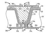
- FIG. 1is a sectional view illustrating a via structure in accordance with an embodiment of the invention.
- FIGS. 2A-2Hare sectional views illustrating stages of fabrication in accordance with the embodiment of the invention depicted in FIG. 1 .
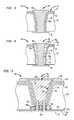
- FIG. 3is a sectional view illustrating a via structure in accordance with another embodiment.
- FIG. 4is a sectional view illustrating a via structure in accordance with another embodiment.
- FIG. 5is a sectional view illustrating a via structure in accordance with another embodiment.
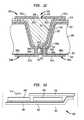
- FIG. 6is a corresponding top-down plan view illustrating a via structure in accordance with the embodiment of the invention depicted in FIG. 1 .
- FIG. 7Ais a corresponding bottom-up plan view illustrating the function of a via structure in accordance with the embodiment of the invention depicted in FIG. 6 .
- FIG. 7Bis a corresponding top-down plan view illustrating the function of a via structure in accordance with the embodiment of the invention depicted in FIG. 7A .
- FIG. 8is a sectional view illustrating a via structure in accordance with another embodiment.
- FIG. 9is a sectional view illustrating a via structure in accordance with another embodiment.
- FIG. 10is a sectional view illustrating a via structure in accordance with another embodiment.
- FIG. 11is a sectional view illustrating a via structure in accordance with another embodiment.
- FIG. 12is a sectional view illustrating a via structure in accordance with another embodiment.
- FIG. 13is a schematic depiction of a system according to one embodiment of the invention.
- FIG. 1is a sectional view illustrating a via structure in accordance with an embodiment of the invention.
- a microelectronic unit 10includes a semiconductor element 20 having an opening 30 extending from a rear surface 22 through the semiconductor element 20 to a front surface 21 remote from the rear surface.
- the directions parallel to front surfaceare referred to herein as “horizontal” or “lateral” directions; whereas the directions perpendicular to the front surface are referred to herein as upward or downward directions and are also referred to herein as the “vertical” directions.
- the directions referred to hereinare in the frame of reference of the structures referred to. Thus, these directions may lie at any orientation to the normal or gravitational frame of reference.
- a statement that one feature is disposed at a greater height “above a surface” than another featuremeans that the one feature is at a greater distance in the same orthogonal direction away from the surface than the other feature.
- a statement that one feature is disposed at a lesser height “above a surface” than another featuremeans that the one feature is at a smaller distance in the same orthogonal direction away from the surface than the other feature.
- a conductive layer 40overlies inner surfaces 31 a , 31 b of the opening 30 and extends along the rear surface 22 . As shown in FIG. 1 , the conductive layer can contact the semiconductor material exposed at surfaces 31 a , 31 b and the conductive layer can extend along surfaces 31 a , 31 b and conform to contours of the surfaces.
- a conductive pad 50can be exposed at the front surface 21 and may at least partially overlie the opening 30 . In a particular embodiment, the conductive pad 50 can be only partially exposed at the front surface 21 .
- a conductive interconnect 60extends within the opening 30 from an inward-facing surface 51 of the conductive pad 50 to lateral edges 66 of a conductive contact 65 exposed at the rear surface 22 that can serve as a contact for electrical connection with an external device.
- the conductive interconnect 60contacts the inward-facing surface 51 at a bottom surface 69 thereof.
- a dielectric layer 24extends along the front surface 21 and electrically insulates the conductive pad 50 from the front surface and the conductive layer 40 .
- a dielectric layer 70overlies the conductive layer 40 inside of the opening 30 and along the rear surface 22 .
- the dielectric layer 70electrically insulates the conductive layer 40 from the conductive interconnect 60 .
- a dielectric region 75occupies the volume between the inner surfaces 61 of the conductive interconnect 60 and an inward-facing surface 67 of the conductive contact 65 .
- the semiconductor element 20can include a semiconductor substrate, which can be made from silicon, for example.
- a plurality of active semiconductor devicese.g., transistors, diodes, etc.
- the conductive pad 50can overlie the semiconductor region 23 a , and the conductive pad 50 can be laterally separated from the semiconductor region 23 b .
- the plurality of active semiconductor devicescan be electrically connected to the conductive pad 50 for interconnection to other internal and/or external components.
- the thickness of the semiconductor element 20 between the front surface 21 and the rear surface 22typically is less than 200 ⁇ m, and can be significantly smaller, for example, 130 ⁇ m, 70 ⁇ m, 50 ⁇ m, or even smaller.
- the semiconductor element 20may be replaced by a nonconductive interposer element, such as a glass substrate or any other dielectric material.
- a nonconductive interposer elementsuch as a glass substrate or any other dielectric material.
- the microelectronic unit 10may be a component that is a circuit element, and the conductive layer 40 and the conductive interconnect 60 may be adapted for electric interconnection with an element external to the component.
- the dielectric layer 24can be located between the front surface 21 and the conductive pad 50 .
- the dielectric layer 24electrically insulates the conductive pad 50 from the semiconductor element 20 and the conductive layer 40 .
- This dielectric layer 24can be referred to as a “passivation layer” of the microelectronic unit 10 .
- the dielectric layer 24can include an inorganic or organic dielectric material or both.
- the dielectric layer 24may include an electrodeposited conformal coating or other dielectric material, for example, a photoimageable polymeric material, for example, a solder mask material.
- the dielectric layer 24may include one or more layers of oxide material or other dielectric material.
- the opening 30extends from the rear surface 22 through the semiconductor element 20 to an inward-facing surface 51 of a conductive pad 50 exposed at the front surface 21 .
- the opening 30includes inner surfaces 31 that extend from the rear surface 22 through the semiconductor element 20 at an angle between 0 and 90 degrees to the horizontal plane defined by the rear surface 22 .
- the inner surface 31can have a constant slope (e.g., as shown in FIG. 5 ) or a varying slope (e.g., as shown in FIG. 1 ).
- the angle or slope of the inner surface 31 relative to the horizontal plane defined by the rear surface 22can decrease in magnitude (i.e., become less positive or less negative) as the inner surface 31 penetrates further towards the front surface 21 .
- the opening 30has a width W 1 at the rear surface 22 and a width W 2 at the front surface 31 that is less than the width W 1 such that the opening is tapered in a direction from the rear surface towards the front surface.
- the openingcan have a constant width, or the opening can be tapered in a direction from the front surface towards the rear surface.
- the opening 30may partially extend from the rear surface 22 towards the front surface 21 , such the opening can be connected to the conductive pad 50 through one or more holes extending therebetween (e.g., as shown in FIG. 5 ).
- the opening 30can have any top-view shape, including for example, an oval shape, a square shape, or a rectangular channel with a plurality of conductive interconnects extending therethrough to respective conductive pads at the front surface of the semiconductor element (not shown).
- the openingcan have a round top-view shape.
- the openingcan have any three-dimensional shape, including for example, a cylinder, a cube, or a prism, among others.
- the conductive layer 40can be made from any electrically conductive metal, including for example, titanium, tungsten, copper, or gold.
- the conductive layer 40extends from the rear surface 22 into the opening 30 , and the conductive layer 40 extends to lower ends 41 that are electrically insulated from the inward-facing surface 51 of the conductive pad 50 by one or more of the dielectric layer 24 , the dielectric layer 70 , or any other dielectric material.
- the conductive layer 40can coat most of the rear surface 22 of the semiconductor element 20 .
- the conductive layer 40may be a continuous layer electrically connected to a reference ground, or the conductive layer may be split with some or all of the areas thereof attached to ground or power.
- the conductive layer 40can serve to electrically shield the conductive interconnects 60 that can carry input and/or output signals, such that the microelectronic unit 10 can experience less signal noise.
- the conductive layer 40can spread heat across the semiconductor element 20 , which can result in improved thermal performance compared to a semiconductor element without such a conductive layer.
- a conductive element that is adapted to be electrically connected to a reference ground input/outputneed not be connected to a single static voltage. Instead of a reference ground, such a conductive element as the conductive layer 40 can be electrically connected to a voltage that can float within a desired voltage range.
- a conductive element as the conductive layer 40need only be insulated from electrical connection with a conductive element that is adapted to be electrically connected to an input and/or output signal (e.g., the conductive interconnect 60 ).
- a conductive element that is adapted to be electrically connected to a reference groundcan be electrically connected to a power input/output.
- a conductive element that is adapted to be electrically connected to a reference grounde.g., the conductive layer 40
- a conductive element that is adapted to be electrically connected to an input and/or output signale.g., the conductive interconnect 60
- an input and/or output signale.g., the conductive interconnect 60
- a conductive layer 40can allow the dielectric layer 70 (or another conductive layer) to be deposited thereon with less process variability (e.g., when using an electrochemical deposition process) than if the dielectric layer was deposited directly onto a substrate element (in place of the semiconductor element 20 ) such as glass.
- non-lithographic techniquesas discussed in greater detail in the co-pending U.S. patent application Ser. No. 12/842,669, filed on Jul. 23, 2010, can be employed.
- Such non-lithographic techniquescan include, for example, selectively treating a surface with a laser or with mechanical processes such as milling or sandblasting so as to treat those portions of the surface along the path where the conductive element is to be formed differently than other portions of the surface.
- a laser or mechanical processmay be used to ablate or remove a material such as a sacrificial layer from the surface only along a particular path and thus form a groove extending along the path.
- a materialsuch as a catalyst can then be deposited in the groove, and one or more metallic layers can be deposited in the groove.
- the semiconductor element 20includes one or more conductive pads 50 exposed at or located at the front surface 21 of the semiconductor element 20 . While not specifically shown in FIG. 1 , the active semiconductor devices in the active semiconductor regions 23 a and 23 b typically are conductively connected to the conductive pads 50 . The active semiconductor devices, thus, are accessible conductively through wiring incorporated extending within or above one or more dielectric layers of the semiconductor element 20 .
- the conductive padsmay not be directly exposed at the front surface of the semiconductor element. Instead, the conductive pads may be electrically connected to traces or other conductive elements extending to terminals that are exposed at the front surface of the semiconductor element.
- the conductive pads 50can be made from any electrically conductive metal, including for example, copper or gold.
- the conductive pads 50 and any of the conductive pads disclosed hereincan have any top-view shape, including a square, round, oval, triangle, rectangle, or any other shape.
- an electrically conductive elementis “exposed at” a surface of a dielectric element indicates that the electrically conductive element is available for contact with a theoretical point moving in a direction perpendicular to the surface of the dielectric element toward the surface of the dielectric element from outside the dielectric element.
- a terminal or other conductive element which is exposed at a surface of a dielectric elementmay project from such surface; may be flush with such surface; or may be recessed relative to such surface and exposed through a hole or depression in the dielectric.
- the conductive interconnect 60extends within the opening 30 and is electrically connected with the conductive pad 50 . As shown in FIG. 1 , the conductive interconnect 60 includes an internal space that is filled with a dielectric region 75 . In exemplary embodiments, the conductive interconnect 60 can be solid, left open, left open and coated with a dielectric layer, or filled with a second conductive material. The conductive interconnect 60 can be made from any electrically conductive metal, including for example, copper or gold.
- the conductive contact 65joined at its lateral edges 66 to the conductive interconnect 60 and is exposed at the outer surface 72 of the dielectric layer 70 for interconnection to an external element. As shown, the conductive contact 65 is located above a plane defined by the outer surface 72 of the dielectric layer 70 and above a plane defined by the rear surface 22 of the semiconductor element 20 . In other embodiments, the conductive contact 65 can be located at or below the plane defined by the outer surface 72 of the dielectric layer 70 , and/or the conductive contact can be located at or below the plane defined by the rear surface 22 .
- the conductive contact 65can be planarized to the outer surface 72 of the dielectric layer 70 or the rear surface 22 , for example, by a grinding, lapping, or polishing process.
- conductive bond materialcan be exposed at the conductive contact 65 or at a surface of another conductive contact exposed at the rear surface of the semiconductor element for interconnection with an external device.
- the microelectronic unit 10includes a semiconductor element 20 having one or more active semiconductor regions 23 a and/or 23 b and having one or more conductive pads 50 exposed at a front surface 21 thereof.
- a support wafer 12is temporarily attached to the front surface 21 of the semiconductor element 20 by an adhesive layer 13 to provide additional structural support to the semiconductor element during processing of the rear surface 22 .
- the thickness of the semiconductor element 20 between the front surface 21 and the rear surface 22can be reduced. Grinding, lapping, or polishing of the rear surface or a combination thereof can be used to reduce the thickness.
- the initial thickness T 1 (shown in FIG. 2B ) of the semiconductor element 20can be reduced from about 700 ⁇ m to a thickness T 2 (shown in FIG. 7G ) of about 50 ⁇ m or less.
- the opening 30can be formed extending downwardly from the rear surface 22 of the semiconductor element 20 to the dielectric layer 24 that extends between the front surface 21 and the inwardly-facing surface 51 of the conductive pad 50 .
- the opening 30can be formed for example, by selectively etching the semiconductor element 20 , after forming a mask layer where it is desired to preserve remaining portions of the rear surface 22 .
- a photoimageable layere.g., a photoresist layer, can be deposited and patterned to cover only portions of the rear surface 22 , after which a timed etch process can be conducted to form the opening 30 .
- the inner surfaces 31 of the opening 30may be sloped, i.e., may extend at angles other a normal angle (right angle) to the rear surface 22 , as shown in FIG. 2D .
- Wet etching processese.g., isotropic etching processes and sawing using a tapered blade, among others, can be used to form openings 30 having sloped inner surfaces 31 .
- Laser dicing, mechanical milling, chemical etching, laser drilling, plasma etching, directing a jet of fine abrasive particles towards the semiconductor element 20 , among others,can also be used to form openings 30 (or any other hole or opening described herein) having sloped inner surfaces 31 .
- the inner surfaces of the opening 30may extend in a vertical or substantially vertical direction downwardly from the rear surface 22 substantially at right angles to the rear surface 22 .
- Anisotropic etching processes, laser dicing, laser drilling, mechanical removal processes, e.g., sawing, milling, ultrasonic machining, directing a jet of fine abrasive particles towards the semiconductor element 20 , among others,can be used to form openings 30 having essentially vertical inner surfaces.
- the opening 30can be located over a plurality of conductive pads 50 located on more than one microelectronic unit 10 , such that when the microelectronic units 10 are severed from each other, a portion of the opening 30 will be located on each microelectronic unit 10 .
- the term “opening”can refer to a opening that is located entirely within a single microelectronic unit, a opening that extends across a plurality of microelectronic units 10 when it is formed (not shown), or a portion of a opening that is located on a particular microelectronic unit 10 after it is severed from other microelectronic units 10 .
- an exemplary methodinvolves depositing a metal layer by one or more of sputtering a primary metal layer onto the rear surface 22 and the inner surfaces 31 a , 31 b , or by electroplating, or mechanical deposition. Electroplating can be performed in a selective manner, such as to form a plated metal layer on the surface of the semiconductor material exposed within the opening 30 and on the rear surface 22 . In such case, the plated metal layer can be made without contacting the conductive pad, which is insulated from the semiconductor element 20 by the passivation layer 24 .
- Mechanical depositioncan involve the directing a stream of heated metal particles at high speed onto the surface to be coated.
- the primary metal layerincludes or consists essentially of aluminum.
- the primary metal layerincludes or consists essentially of copper.
- the primary metal layerincludes or consists essentially of titanium.
- One or more other exemplary metalscan be used in a process to form the conductive layer 40 .
- a stack including a plurality of metal layerscan be formed on one or more of the afore-mentioned surfaces.
- such stacked metal layerscan include a layer of titanium followed by a layer of copper overlying the titanium (Ti—Cu), a layer of nickel followed by a layer of copper overlying the nickel layer (Ni—Cu), a stack of nickel-titanium-copper (Ni—Ti—Cu) provided in similar manner, or a stack of nickel-vanadium (Ni—V), for example.
- a dielectric layer 70can be deposited onto the conductive layer 40 overlying the rear surface 22 of the semiconductor element 20 and overlying the inner surfaces 31 of the opening 30 .
- the dielectric layer 70conforms to a contour of the conductive layer 40 , and, because the conductive layer 40 conforms to a contour of the inner surfaces 31 of the opening 30 , the dielectric layer also conforms to a contour of the inner surfaces of the opening.
- the passivation layer 24can be present between the dielectric layer 70 and the conductive pad 50 .
- a flowable dielectric materialis applied to the conductive layer 40 overlying the rear surface 22 , and the flowable material is then more evenly distributed across the rear surface during a “spin-coating” operation, followed by a drying cycle which may include heating.
- a thermoplastic film of dielectric materialcan be applied to the rear surface 22 of after which the semiconductor element is heated, or is heated in a vacuum environment, i.e., placed in an environment under lower than ambient pressure. This then causes the film to flow downward onto the inner surfaces 31 of the opening 30 .
- vapor depositioncan be used to form the dielectric layer 70 .
- the semiconductor element 20can be immersed in a dielectric deposition bath to form a conformal dielectric coating or dielectric layer 70 .
- a “conformal coating”is a coating of a particular material that conforms to a contour of the surface being coated, such as when the dielectric layer 70 conforms to a contour of the conductive layer 40 .
- An electrochemical deposition methodcan be used to form the conformal dielectric layer 70 , including for example, electrophoretic deposition or electrolytic deposition.
- an electrophoretic deposition techniquecan be used to form the conformal dielectric coating, such that the conformal dielectric coating is only deposited onto exposed conductive and semiconductive surfaces of the assembly.
- the semiconductor device waferis held at a desired electric potential and an electrode is immersed into the bath to hold the bath at a different desired potential.
- the assemblyis then held in the bath under appropriate conditions for a sufficient time to form an electrodeposited conformal dielectric layer 70 on exposed surfaces of the conductive layer 40 , including but not limited to overlying the rear surface 22 and the inner surfaces 31 .
- Electrophoretic depositionoccurs so long as a sufficiently strong electric field is maintained between the surface to be coated thereby and the bath.
- the electrophoretically deposited coatingis self-limiting in that after it reaches a certain thickness governed by parameters, e.g., voltage, concentration, etc. of its deposition, deposition stops.
- Electrophoretic depositionforms a continuous and uniformly thick conformal coating on conductive and/or semiconductive exterior surfaces of the assembly (e.g., the conductive layer 40 ).
- the electrophoretic coatingcan be deposited so that it does not form on pre-existing dielectric layers such as the dielectric layer 24 , due to its dielectric (nonconductive) property.
- a property of electrophoretic depositionis that is does not form on a layer of dielectric material overlying a conductor provided that the layer of dielectric material has sufficient thickness, given its dielectric properties.
- electrophoretic depositionwill not occur on dielectric layers having thicknesses greater than about 10 microns to a few tens of microns.
- the conformal dielectric layer 70can be formed from a cathodic epoxy deposition precursor. Alternatively, a polyurethane or acrylic deposition precursor could be used.
- a variety of electrophoretic coating precursor compositions and sources of supplyare listed in Table 1 below.
- the dielectric layercan be formed electrolytically. This process is similar to electrophoretic deposition, except that the thickness of the deposited layer is not limited by proximity to the conductive or semiconductive surface from which it is formed. In this way, an electrolytically deposited dielectric layer can be formed to a thickness that is selected based on requirements, and processing time is a factor in the thickness achieved.
- the passivation layer 24can be removed before the dielectric layer 70 is formed by electrolytic or electrophoretic deposition onto the conductive layer 40 . This is possible because the deposition can be performed selectively onto the exposed surface of the conductive layer 40 , without depositing the dielectric layer 70 on the inwardly-facing surface 51 of the conductive pad 50 .
- an etch processcan be conducted in a manner that selectively etches the portion of the dielectric layer 24 (the passivation layer) that is exposed within the opening 30 , thereby extending the opening to expose the inwardly-facing surface 51 of the conductive pad 50 .
- Etching, laser drilling, mechanical milling, or other appropriate techniquescan be used to remove the portion of the passivation layer 24 .
- the etching of the dielectric layer 24does not expose the lower ends 41 of the conductive layer 40 , such that the lower ends are still insulated from the conductive pad 50 by a remaining portion of the dielectric layer 24 and a portion of the dielectric layer 70 .
- dielectric layer removal techniquesinclude various selective etching techniques which can be isotropic or anisotropic in nature.
- Anisotropic etch processesinclude reactive ion etch processes in which a stream of ions are directed towards surfaces to be etched.
- Reactive ion etch processesare generally less selective than isotropic etch processes such that surfaces at which ions strike at high angles of incidence are etched to a greater extent than surfaces which are oriented with the stream of ions.
- a mask layeris desirably deposited to overlie the passivation layer 24 and an opening is formed therein that is aligned with the opening 30 . In such a way, the etch process avoids removing portions of the passivation layer 24 other than that which lies within the opening 30 .
- the conductive interconnect 60is deposited into the opening 30 onto the portion of the dielectric layer 70 that is located within the opening and onto the inwardly-facing surface 51 of the conductive pad 50 , thereby electrically connecting the conductive interconnect to the conductive pad.
- the shape of the conductive interconnect 60conforms to a contour of the outer surface 72 of the dielectric layer 70 and a contour of the inwardly-facing surface 51 of the conductive pad 50 .
- the conductive interconnect 60also conforms to a contour of the conductive layer and a contour of the inner surfaces of the opening.
- the conductive interconnect 60is deposited onto the outer surface 72 of the dielectric layer 70 such that an internal space 62 is created inside the conductive interconnect.
- the conductive interconnect 60can be formed using one or more of the metal layer deposition processes described above with reference to deposition of the conductive layer 40 , for example, an exemplary method involves depositing a metal layer by one or more of sputtering a primary metal layer onto the outer surface 72 and the inwardly-facing surface 51 , plating, or mechanical deposition.
- the internal space 62can be filled with a dielectric region 75 .
- the dielectric region 75can be formed such that an exposed outer surface 76 of the dielectric region is parallel to or substantially parallel to the rear surface 22 of the semiconductor element or the exposed portion of the outer surface 72 of the dielectric layer 70 .
- a self-planarizing dielectric materialcan be deposited in the opening 30 , e.g., by a dispensing or stenciling process.
- a grinding, lapping, or polishing processcan be applied to the exposed outer surface 76 of the dielectric region 75 after forming the dielectric region to planarize the outer surface thereof.
- the conductive contact 65can be formed, for example, by plating the conductive contact onto the outer surface 75 of the dielectric region 75 .
- the conductive contact 65is exposed at the outer surface 76 of the dielectric region 75 for interconnection with an external device.
- the conductive contact 65is electrically connected at its lateral edges 66 to the upper edges of the conductive interconnect 60 .
- the support wafer 12can be removed from the front surface 21 of the semiconductor element 20 .
- FIG. 3is a sectional view illustrating a variation of the via structure of FIG. 1 having an alternate conductive interconnect configuration.
- the microelectronic unit 10 ais similar to the microelectronic unit 10 described above, but rather than having a conductive interconnect that is filled with a dielectric region that is surrounded by the conductive interconnect and a conductive contact that is exposed at the rear surface, the microelectronic unit 10 a has a solid conductive interconnect 60 a that fills all of the volume within the opening 30 that is not occupied by the conductive layer 40 and the dielectric layer 70 .
- An outwardly-facing surface 65 a of the conductive interconnect 60 ais exposed at the outer surface 72 of the dielectric layer 70 for interconnection to an external element.
- the exposed outwardly-facing surface 65 acan be the top surface of the conductive interconnect 60 a , i.e., a surface at a furthest extent from the conductive pad 50 , or the exposed surface may not be a top surface thereof.
- the outwardly-facing surface 65 ais located above a plane defined by the outer surface 72 of the dielectric layer 70 and above a plane defined by the rear surface 22 of the semiconductor element 20 .
- the outwardly-facing surface 65 acan be located at or below the plane defined by the outer surface 72 of the dielectric layer 70 , and/or the outwardly-facing surface 65 a can be located at or below the plane defined by the rear surface 22 .
- the outwardly-facing surface 65 acan be planarized to the outer surface 72 of the dielectric layer 70 or the rear surface 22 , for example, by a grinding, lapping, or polishing process.
- FIG. 4is a sectional view illustrating another variation of the via structure of FIG. 3 having an alternate conductive interconnect configuration.
- the microelectronic unit 10 bis similar to the microelectronic unit 10 a described above, but rather than having a conductive interconnect that fills the space inside of the opening that is not occupied by the conductive layer or the dielectric layer, the microelectronic unit 10 b has a conductive interconnect 60 b that is deposited into a first aperture 71 formed in a dielectric region 75 b located within the opening 30 .
- the dielectric region 75 bcan provide good dielectric isolation with respect to the conductive interconnect 60 b and the conductive layer 40 . As shown in FIG. 4 , the dielectric region 75 b covers an outer surface 42 of the conductive layer 40 , both inside the opening 30 and along the rear surface 22 of the semiconductor element 20 . The dielectric region 75 b can electrically insulate the conductive interconnect 60 b from the conductive layer 40 .
- the dielectric region 75 bcan be compliant, having a sufficiently low modulus of elasticity and sufficient thickness such that the product of the modulus and the thickness provide compliancy. Specifically, such a compliant dielectric region 75 b can allow the conductive interconnect 60 b and the conductive contact 65 b attached thereto to flex or move somewhat relative to the semiconductor element 20 when an external load is applied to the conductive contact. In that way, the bond between the conductive contacts 65 b of the microelectronic unit 10 b and terminals of a circuit panel (not shown) can better withstand thermal strain due to mismatch of the coefficient of thermal expansion (“CTE”) between the microelectronic unit and the circuit panel.
- CTEcoefficient of thermal expansion
- the dielectric region 75 bcan fill the remainder of the opening 30 that is not occupied by the conductive interconnect 60 b or the conductive layer 40 , such that an outer surface 76 b extends above a plane defined by the rear surface 22 of the semiconductor element 20 and above a plane defined by the outer surface 42 of the portion of the conductive layer that extends along the rear surface of the semiconductor element.
- the outer surface 76 b of the dielectric region 75 bcan be located at or below the plane defined by the rear surface 22 or at or below the plane defined by the outer surface 42 of the portion of the conductive layer 40 that extends along the rear surface.
- the first aperture 71is provided in the dielectric region 75 b .
- the first aperture 71has a frusto-conical shape and extends through the dielectric region 75 b from an inward-facing surface 67 b of the conductive contact 65 b to the inward-facing surface 51 of the conductive pad 50 .
- the first aperturecan have other shapes, including for example, a cylindrical shape or a combination of a cylindrical and a frusto-conical shape at different distances from the rear surface.
- a contour of the first aperture 71i.e., the shape of the outer surface of the first aperture 71 ) does not conform to a contour of the opening 30 or a contour of the conductive layer 40 .
- the conductive interconnect 60 bcan be formed either solid or hollow depending upon the process conditions. Under appropriate process conditions, a conductive interconnect that includes an internal space can be produced, and that internal space can then be filled with a dielectric material or a second conductive material, whereby the dielectric layer or the second conductive material overlies the conductive interconnect within the first aperture.
- the conductive contact 65 bcan be aligned with the opening 30 and can be disposed wholly or partly within an area of the semiconductor element 20 defined by the opening.
- a plane defined by a top surface 68 of the conductive contact 65 bis substantially parallel to the plane defined by the rear surface 22 of the semiconductor element 20 .
- the conductive contact 65 bhas the shape of a conductive bond pad, e.g., a thin flat member.
- the conductive contactcan be any other type of conductive contact, including for example, a conductive post.
- FIG. 5is a sectional view illustrating a via structure in accordance with another embodiment having a plurality of holes extending from the same opening.
- a microelectronic unit 110includes a semiconductor element 120 having an opening 130 extending from a rear surface 122 partially through the semiconductor element 120 towards a front surface 121 remote from the rear surface.
- a conductive layer 140extends conformally along the rear surface 122 and into the opening 130 , the conductive layer conformally coating inner surfaces 131 of the opening and extending to lower ends 141 located adjacent a lower surface 132 of the opening.
- the semiconductor element 120also has a plurality of holes 180 extending from respective conductive pads 150 exposed at the front surface 121 and partially overlying the opening 130 .
- the holes 180meet the opening 130 at a location between the front surface 121 and the rear surface 122 .
- Each conductive via 190extends from a respective conductive pad 150 to a respective conductive interconnect 160 within a respective hole 180 and conforms to a contour of an inner surface 181 thereof. As shown in FIG. 5 , each conductive via 190 extends from an inwardly-facing surface 151 of a respective conductive pad 150 . In a particular embodiment, each conductive via 190 can extend through a respective conductive pad 150 and can contact the conductive pad 150 at least at an outwardly-facing surface 152 thereof.
- Each conductive via 190can fill all of the volume within a respective hole 180 inside of a conformal dielectric layer 187 that electrically insulates the semiconductor element 120 from the conductive via, such that each conductive via can be conformal to a contour of the inner surface 181 of the respective hole.
- a dielectric layer 170conformally overlies the conductive layer 140 inside of the opening 130 and along the rear surface 122 .
- the dielectric layer 170electrically insulates the conductive interconnects 160 from the conductive layer 140 .
- the dielectric layer 170also extends along and is conformal to the lower surface 132 of the opening 130 , although another dielectric layer 179 may be disposed between the dielectric layer 170 and the lower surface.
- the dielectric layers 170 and 179can electrically insulate the conductive interconnects 160 from the silicon material of the lower surface 132 that is not coated by the conductive layer 140 .
- a dielectric layer 124extends along the front surface 121 and electrically insulates the conductive pads 150 from the semiconductor element 120 .
- a dielectric region 175occupies the volume between inner surfaces 161 of the conductive interconnects 160 and inward-facing surfaces 167 of the conductive contacts 165 , such that an outer surface 176 of the dielectric region extends above but is parallel to a plane defined by the rear surface 122 of the semiconductor element 120 .
- the conductive layer 140can coat most of the rear surface 122 of the semiconductor element 120 .
- the conductive layer 140can serve to electrically shield the conductive interconnects 160 and the respective conductive vias 190 attached thereto that can carry input and/or output signals, such that the microelectronic unit 110 can experience less signal noise.
- FIG. 6illustrates a microelectronic unit 10 c that can be one potential top-down plan view of the microelectronic unit 10 shown in FIG. 1 .
- the microelectronic element 10 cincludes four openings 30 extending through a single semiconductor element 20 , each opening having a substantially round top-view shape.
- Each opening 30includes a conductive interconnect 60 extending therethrough from a round-shaped conductive contact 65 exposed at the rear surface 22 of the semiconductor element 20 to a bottom surface 69 of the conductive interconnect attached to a corresponding square-shaped conductive pad 50 .
- four openings 30are shown in the microelectronic unit 10 c , the microelectronic units described herein can have any number of openings extending through a single semiconductor element.
- FIG. 7Aillustrates a microelectronic unit 10 d that can be one potential functional view of the front surface 21 of the semiconductor element 20 of the microelectronic unit 10 c shown in FIG. 6 .
- the microelectronic element 10 dincludes four square-shaped conductive pads 50 a and 50 b , each conductive pad at least partially overlying a corresponding opening in a single microelectronic element 20 , for example, such as the arrangement of openings shown in FIG. 6 .
- each conductive pads 50 ais electrically connected to a respective conductive interconnect that can carry input and/or output signals, such as the conductive interconnect 60 shown in FIG. 1 .
- Each conductive pad 50 bis electrically connected to a conductive layer that may be a continuous layer attached to a reference ground, or the conductive layer may be split with some or all of the areas thereof attached to ground or power, such as the conductive layer 40 shown in FIG. 1 .
- the conductive pads 50 acan carry input and/or output signals, while the conductive pads 50 b can be electrically connected to a reference ground.
- the conductive pads 50 bcan be attached to a respective conductive interconnect in addition to a conductive layer, wherein both the conductive interconnect and the conductive layer can be electrically connected, for example, to a reference ground.
- FIG. 7Billustrates a microelectronic unit 10 d that can be one potential functional view of the rear surface 22 of the semiconductor element 20 of the microelectronic unit 10 c shown in FIG. 6 .
- the microelectronic element 10 dincludes a conductive layer 40 that coats most of the rear surface 22 .
- the conductive layer 40can be electrically connected with the conductive pads 50 b at the front surface 21 (shown in FIG. 7A ).
- the conductive layer 40can be directly connected with the conductive pads (e.g., as shown in FIGS. 8-11 ).
- the conductive layer 40functionally extends across the entire rear surface 22 and the inner surfaces of the openings, except at the portions of the conductive pads 50 a that are exposed at the lower ends 41 of the conductive layer.
- FIG. 8is a sectional view illustrating a variation of the via structure of FIG. 3 having an alternate conductive interconnect configuration that is suitable for connection to a reference ground.
- a via structure as shown in FIG. 8can be used, for example, to electrically connect a conductive pad such as the conductive pad 50 b shown in FIG. 7A to a conductive layer such as the conductive layer 40 shown in FIG. 7B , wherein both the conductive pad and the conductive layer are electrically connected to a reference ground.
- the microelectronic unit 210is similar to the microelectronic unit 10 a described above, but rather than having a conductive interconnect that is electrically isolated from a conductive layer by one or more dielectric layers, the microelectronic unit 210 has a conductive interconnect 260 that is electrically connected to a conductive layer 240 .
- Lower ends 241 of the conductive layer 240are connected to the conductive interconnect 260 adjacent the bottom surface 269 thereof.
- a dielectric layer 270 that extends conformally along the conductive layer 240terminates adjacent the lower ends 241 thereof, such that when the conductive interconnect 260 is plated onto the dielectric layer, the conductive interconnect is formed with a connection to the lower ends of the conductive layer.
- the conductive interconnect 260is electrically connected with a conductive pad 250 exposed at the front surface 221 of the semiconductor element 220 .
- An outwardly-facing surface 265 of the conductive interconnect 260is exposed at the outer surface 272 of the dielectric layer 270 for interconnection to an external element.
- a reference groundcan be connected to the conductive pad 250 or the outwardly-facing surface 265 , and the reference ground will also be electrically connected to the conductive layer 240 through the conductive interconnect 260 .
- the structure shown in FIG. 8can be fabricated simultaneously with the fabrication of other structures having dual insulated conductors (such as shown for example in FIG. 1 , 3 , or 4 ) using a variation of the fabrication process described above with reference to FIGS. 2A-2H .
- the passivation layer 24can be removed where exposed within the opening 30 .
- processingcould continue as shown and described above with respect to FIGS. 2E-2H .
- the conductive layer 40directly contacts the surface 51 of the conductive pad 50 .
- a resist layercan be deposited and patterned to cover portions of the rear surface 22 and some but not all of the openings 30 therein.
- the passivation layer 24can be removed from only the openings where the reference conductor structure such as shown in FIG. 8 is to be formed. After removing the passivation layer 24 from particular openings, the resist layer can then be removed.
- the metal layer 240e.g., that of FIG. 8
- itwill then be a continuous layer which contacts the conductive pad 250 and the interior surface of the semiconductor element within the opening 230 .
- the metal layer 40 in other structuressuch as that shown in FIG. 1 , that is formed simultaneously with the metal layer 240 will be insulated from the respective conductive pad 50 .
- FIG. 9is a sectional view illustrating a variation of the via structure of FIG. 4 having an alternate conductive interconnect configuration that is suitable for connection to a reference ground.
- the electrical structure of the microelectronic unit 210 ai.e., providing a conductive interconnect that is electrically connected to a conductive layer
- FIG. 8The electrical structure of the microelectronic unit 210 a (i.e., providing a conductive interconnect that is electrically connected to a conductive layer) is similar to the electrical structure of the microelectronic unit 210 shown in FIG. 8 .
- the microelectronic unit 210 ais similar to the microelectronic unit 10 b described above, but rather than having a conductive interconnect that is electrically isolated from a conductive layer by one or more dielectric layers, the microelectronic unit 210 a has a conductive interconnect 260 a that is electrically connected to a conductive layer 240 .
- Lower ends 241 of the conductive layer 240are connected to the conductive interconnect 260 a adjacent the bottom surface 269 a thereof.
- the conductive interconnect 260 ais electrically connected with a conductive pad 250 exposed at the front surface 221 of the semiconductor element 220 .
- a conductive contact 265 a attached to the conductive interconnect 260 ais exposed at the outer surface 276 of the dielectric region 275 for interconnection to an external element.
- a reference groundcan be connected to the conductive pad 250 or the conductive contact 265 a , and the reference ground will also be electrically connected to the conductive layer 240 through the conductive interconnect 260 a.
- FIG. 10is a sectional view illustrating a variation of the via structure of FIG. 9 that is suitable for connection to a reference ground.
- the microelectronic unit 210 bis similar to the microelectronic unit 210 a described above.
- the conductive contact 265 bcan be electrically connected to the conductive pad 250 through the conductive layer 240 b that contacts the surface of the semiconductor element within openings 230 .
- the conductive contact 265 bis connected with the conductive layer 240 b at lateral edges 266 of the conductive contact.
- a dielectric region 275 bmay fill all of the volume within the opening 230 that is not occupied by the conductive layer 240 .
- the conductive contact 265 bis exposed at a surface, e.g., an outer surface 276 b of the dielectric region 275 b for interconnection with an external device.
- a conductive pad 250 or the conductive contact 265 bcan be connected to a source of power, ground or other reference potential, and the reference potential will also be electrically connected to the conductive layer 240 that extends therebetween and along the rear surface 222 of the semiconductor element 220 .
- FIG. 11is a sectional view illustrating a variation of the via structure of FIG. 10 having a solid conductive region that is suitable for connection to a reference ground.
- the microelectronic unit 210 cis similar to the microelectronic unit 210 b described above, but rather than having a conductive layer that is electrically connected to a conductive pad and a conductive contact with a dielectric region filling the volume therebetween, the microelectronic unit 210 b includes a solid conductive region 240 c that fills all of the volume within an opening 230 extending through a thickness of a semiconductor element 220 .
- the microelectronic unit 210 cdoes not have a separate conductive contact that is connected with a conductive pad through a conductive layer. Instead, the solid conductive region 240 c extends along a rear surface 222 of the semiconductor element 220 and extends through the opening 230 , contacting the conductive pad 250 at an inwardly-facing surface 251 thereof. The conductive region 240 c has an outwardly-facing surface 265 c thereof that is exposed at the rear surface 222 for electrical interconnection with an external device.
- a reference groundcan be connected to the conductive pad 250 or the outwardly-facing surface 265 c , and the reference ground will also be electrically connected to the conductive region 240 that extends therebetween and along the rear surface 222 .
- FIG. 12is a sectional view illustrating a via structure in accordance with another embodiment having a plurality of holes 380 a , 380 b which extend from the same opening 300 in the semiconductor element.
- a signal connection and a reference conductor connectione.g., a connection for carrying a signal and a connection to a source of ground or power
- These connectionscan be electrically insulated from one another.
- a microelectronic unit 310includes a semiconductor element 320 having an opening 330 extending from a rear surface 322 partially through the semiconductor element 320 towards a front surface 321 remote from the rear surface.
- a conductive layer 340extends conformally along the rear surface 322 and into the opening 330 , the conductive layer conformally coating inner surfaces 331 and a portion of a lower surface 332 of the opening and extending to lower ends 341 a located adjacent the lower surface of the opening and 341 b located at the lower surface of the opening.
- the semiconductor element 320also has a plurality of holes 380 a and 380 b extending from respective conductive pads 350 a and 350 b exposed at the front surface 321 and partially overlying the opening 330 .
- Each of the holes 380 a and 380 bmeets the opening 330 at a location between the front surface 321 and the rear surface 322 .
- the holescan be separated from each other by semiconductor material within the semiconductor element. In a variation thereof, the holes can be separated from each other by dielectric material (not shown) between them or by a combination of the semiconductor material and dielectric material.
- Vias 390 a and 390 bextend within respective holes 380 a , 380 b . The vias can conform to the contours of the interior surfaces of the holes.
- each conductive via 390 a and 390 bextends from an inwardly-facing surface 351 a and 351 b of a respective conductive pad 350 a and 350 b .
- each conductive via 390 a and 390 bcan extend through a respective conductive pad 350 a and 350 b and can contact the conductive pad at least at a respective outwardly-facing surface 352 a and 352 b thereof.
- the conductive via 390 acan fill all of the volume within the hole 380 a inside of a conformal dielectric layer 387 that electrically insulates the semiconductor element 320 from the conductive via, such that the conductive via can be conformal to a contour of the inner surface of the hole.
- the conductive via 390 bcan fill all of the volume within a respective hole 380 b , such that the conductive via can be conformal to a contour of the inner surface of the hole. In the case of via 390 b , there need not be a dielectric layer insulating it from an interior surface of the hole 380 b.
- Each conductive pad 350 a and 350 bis electrically connected to a respective conductive contact 365 a and 365 b exposed at the rear surface 322 for electrical connection with an external device.
- the electrical connection between the conductive pad 350 a and the conductive contact 365 ais through a conductive interconnect 360 and a conductive via 390 a .
- the electrical connection between the conductive pad 350 b and the conductive contact 365 bis through conductive layer 340 and conductive via 390 b .
- the conductive interconnect 360can extend within the opening 330 between the conductive via 390 a and the conductive contact 365 a and can conform to a contour of an inner surface 331 of the opening.
- a dielectric layer 370can conform to a contour of a surface of the conductive layer 340 inside the opening 330 and along the rear surface 322 .
- the dielectric layer 370can electrically insulate the conductive interconnect 360 from the conductive layer 340 .
- the dielectric layer 370can also extend along and conform to a contour of the lower surface 332 of the opening 330 , although another dielectric layer 379 may be disposed between the dielectric layer 370 and the lower surface.
- the dielectric layers 370 and 379can electrically insulate the conductive interconnect 360 from the silicon material of the lower surface 332 that is not coated by the conductive layer 340 .
- a dielectric layer 324(e.g., a “passivation layer”) can extend along the front surface 321 and electrically insulates the conductive pads 350 a and 350 b from the semiconductor element 320 , although the conductive pad 350 b can be electrically connected with the semiconductor element through the conductive layer 340 .
- a dielectric region 375occupies the volume between an inner surface 361 of the conductive interconnect 360 , the exposed outer surface 372 of the dielectric layer 370 , and inward-facing surfaces 367 a and 367 b of the conductive contacts 365 a and 365 b , such that an outer surface 376 of the dielectric region extends above but is parallel to a plane defined by the rear surface 322 of the semiconductor element 320 .
- the conductive layer 340can coat most of the rear surface 322 of the semiconductor element 320 .
- the conductive layer 340can serve as a reference conductor of a transmission line which is adapted to carry a signal through the semiconductor element by way of the via 390 a and conductive interconnect 360 . In this way, a desired impedance can be achieved for such transmission line.
- the conductive layer 340may electrically shield the conductive interconnect 360 and the respective conductive via 390 a attached thereto in the transmission of a signal.
- a reference ground or power input/outputcan be connected to the conductive pad 350 b or the conductive contact 365 b , and the reference ground or power input/output will also be electrically connected to the conductive layer 340 that extends therebetween.
- the methods disclosed herein for forming via structures in semiconductor elementscan be applied to a microelectronic substrate, such as a single semiconductor chip, or can be applied simultaneously to a plurality of individual semiconductor chips which can be held at defined spacings in a fixture or on a carrier for simultaneous processing.
- the methods disclosed hereincan be applied to a microelectronic substrate or element including a plurality of semiconductor chips which are attached together in form of a wafer or portion of a wafer to perform processing as described above simultaneously with respect to a plurality of semiconductor chips on a wafer-level, panel-level or strip-level scale.
- the structures discussed aboveprovide extraordinary three-dimensional interconnection capabilities. These capabilities can be used with chips of any type. Merely by way of example, the following combinations of chips can be included in structures as discussed above: (i) a processor and memory used with the processor; (ii) plural memory chips of the same type; (iii) plural memory chips of diverse types, such as DRAM and SRAM; (iv) an image sensor and an image processor used to process the image from the sensor; (v) an application-specific integrated circuit (“ASIC”) and memory.
- ASICapplication-specific integrated circuit
- a system 400 in accordance with a further embodiment of the inventionincludes a structure 406 as described above in conjunction with other electronic components 408 and 410 .
- component 408is a semiconductor chip whereas component 410 is a display screen, but any other components can be used.
- the systemmay include any number of such components.
- the structure 406 as described abovemay be, for example, a microelectronic unit as discussed above in connection with FIG. 1 , or a structure incorporating plural microelectronic units. In a further variant, both may be provided, and any number of such structures may be used.
- Structure 406 and components 408 and 410are mounted in a common housing 401 , schematically depicted in broken lines, and are electrically interconnected with one another as necessary to form the desired circuit.
- the systemincludes a circuit panel 402 such as a flexible printed circuit board, and the circuit panel includes numerous conductors 404 , of which only one is depicted in FIG. 13 , interconnecting the components with one another.
- thisis merely exemplary; any suitable structure for making electrical connections can be used.
- the housing 401is depicted as a portable housing of the type usable, for example, in a cellular telephone or personal digital assistant, and screen 410 is exposed at the surface of the housing.
- structure 406includes a light-sensitive element such as an imaging chip, a lens 411 or other optical device also may be provided for routing light to the structure.
- FIG. 13the simplified system shown in FIG. 13 is merely exemplary; other systems, including systems commonly regarded as fixed structures, such as desktop computers, routers and the like can be made using the structures discussed above.
- the vias and via conductors disclosed hereincan be formed by processes such as those disclosed in greater detail in the co-pending, commonly assigned U.S. patent application Ser. Nos. 12/842,717, 12/842,651, 12/842,612, 12/842,669, 12/842,692, and 12/842,587, filed on Jul. 23, 2010, and in published U.S. Patent Application Publication No. 2008/0246136, the disclosures of which are incorporated by reference herein.
Landscapes
- Engineering & Computer Science (AREA)
- Computer Hardware Design (AREA)
- Microelectronics & Electronic Packaging (AREA)
- Power Engineering (AREA)
- Physics & Mathematics (AREA)
- Condensed Matter Physics & Semiconductors (AREA)
- General Physics & Mathematics (AREA)
- Manufacturing & Machinery (AREA)
- Geometry (AREA)
- Internal Circuitry In Semiconductor Integrated Circuit Devices (AREA)
Abstract
Description
- The present application is a divisional of U.S. patent application Ser. No. 12/884,695, filed Sep. 17, 2010, the disclosure of which is incorporated herein by reference.
- The present invention relates to packaging of microelectronic devices, especially the packaging of semiconductor devices.
- Microelectronic elements generally comprise a thin slab of a semiconductor material, such as silicon or gallium arsenide, commonly called a die or a semiconductor chip. Semiconductor chips are commonly provided as individual, prepackaged units. In some unit designs, the semiconductor chip is mounted to a substrate or chip carrier, which is in turn mounted on a circuit panel, such as a printed circuit board.
- The active circuitry is fabricated in a first face of the semiconductor chip (e.g., a front surface). To facilitate electrical connection to the active circuitry, the chip is provided with bond pads on the same face. The bond pads are typically placed in a regular array either around the edges of the die or, for many memory devices, in the die center. The bond pads are generally made of a conductive metal, such as copper, or aluminum, around 0.5 μm thick. The bond pads could include a single layer or multiple layers of metal. The size of the bond pads will vary with the device type but will typically measure tens to hundreds of microns on a side.
- Through-silicon vias (TSVs) are used to connect the bond pads with a second face of the semiconductor chip opposite the first face (e.g., a rear surface). A conventional via includes a hole penetrating through the semiconductor chip and a conductive material extending through the hole from the first face to the second face. The bond pads may be electrically connected to vias to allow communication between the bond pads and conductive elements on the second face of the semiconductor chip.
- Conventional TSV holes may reduce the portion of the first face that can be used to contain the active circuitry. Such a reduction in the available space on the first face that can be used for active circuitry may increase the amount of silicon required to produce each semiconductor chip, thereby potentially increasing the cost of each chip.
- Conventional vias may have reliability challenges because of a non-optimal stress distribution inside of the vias and a mismatch of the coefficient of thermal expansion (CTE) between a semiconductor chip, for example, and the structure to which the chip is bonded. For example, when conductive vias within a semiconductor chip are insulated by a relatively thin and stiff dielectric material, significant stresses may be present within the vias. In addition, when the semiconductor chip is bonded to conductive elements of a polymeric substrate, the electrical connections between the chip and the higher CTE structure of the substrate will be under stress due to CTE mismatch.
- Size is a significant consideration in any physical arrangement of chips. The demand for more compact physical arrangements of chips has become even more intense with the rapid progress of portable electronic devices. Merely by way of example, devices commonly referred to as “smart phones” integrate the functions of a cellular telephone with powerful data processors, memory and ancillary devices such as global positioning system receivers, electronic cameras, and local area network connections along with high-resolution displays and associated image processing chips. Such devices can provide capabilities such as full internet connectivity, entertainment including full-resolution video, navigation, electronic banking and more, all in a pocket-size device. Complex portable devices require packing numerous chips into a small space. Moreover, some of the chips have many input and output connections, commonly referred to as “I/O's.” These I/O's must be interconnected with the I/O's of other chips. The interconnections should be short and should have low impedance to minimize signal propagation delays. The components which form the interconnections should not greatly increase the size of the assembly. Similar needs arise in other applications as, for example, in data servers such as those used in internet search engines. For example, structures which provide numerous short, low-impedance interconnects between complex chips can increase the bandwidth of the search engine and reduce its power consumption.
- Despite the advances that have been made in semiconductor via formation and interconnection, further improvements can still be made.
- In accordance with an aspect of the invention, a microelectronic unit can include a semiconductor element consisting essentially of semiconductor material and having a front surface, a rear surface, a plurality of active semiconductor devices adjacent the front surface, a plurality of conductive pads exposed at the front surface, and an opening extending through the semiconductor element. At least one of the conductive pads can at least partially overlie the opening and can be electrically connected with at least one of the active semiconductor devices. The microelectronic unit can also include a first conductive element exposed at the rear surface for connection with an external component. The first conductive element can extend through the opening and can be electrically connected with the at least one conductive pad. The microelectronic unit can also include a second conductive element extending through the opening and insulated from the first conductive element. The at least one conductive pad can overlie a peripheral edge of the second conductive element.
- In a particular embodiment, the second conductive element can be connectable to a reference potential. In one embodiment, the first and second conductive elements can be arranged to permit a desired impedance to be achieved for carrying a signal by the first conductive element. In an exemplary embodiment, the first and second conductive elements can be arranged to improve electrical parasitics such as reducing cross-talk or improving signal to noise ratio. In a particular embodiment, the opening can extend completely through a thickness of the semiconductor element. In one embodiment, the first and second conductive elements can be arranged to permit a desired impedance to be achieved for a signal carried by the first conductive element. In an exemplary embodiment, the at least one conductive pad can have an inwardly-facing surface remote from the exposed surface of the conductive pad, and the edge of the second conductive element can be disposed below a height defined by the inwardly-facing surface of the conductive pad.
- In one embodiment, the second conductive element can extend along an interior surface of the opening and the first conductive element can be separated from the second conductive element by a thickness of a dielectric layer therebetween. In a particular embodiment, the dielectric layer can include an aperture exposing the at least one conductive pad. The aperture can have a contour that at least does not fully conform to a contour of the interior surface of the opening. The first conductive element can be disposed in the aperture. In an exemplary embodiment, the second conductive element can contact an interior surface of the opening. In one embodiment, the second conductive element can be deposited onto the interior surface of the opening. In a particular embodiment, the second conductive element can be deposited by at least one of plating, physical and/or chemical vapor deposition, physical and/or chemical plasma deposition, a Bosch process, and atomic layer deposition.
- In an exemplary embodiment, the second conductive element can at least substantially surround the first conductive element. In one embodiment, the second conductive element can conform to a contour of an interior surface of the opening. In a particular embodiment, a dielectric layer between the first and second conductive elements can have a surface which conforms to a contour of a surface of the interior surface of the opening. The first conductive element can be formed on the surface of the dielectric layer, such that the first conductive element can conform to a contour of the interior surface of the opening. In an exemplary embodiment, the second conductive element can be separated from the at least one conductive pad by at least one dielectric layer disposed therebetween. In one embodiment, the first conductive element can include a contact portion exposed at the rear surface. The contact portion can at least partially overlie the at least one conductive pad to which it is electrically connected.
- In a particular embodiment, the contact portion can fully overlie the at least one conductive pad to which it is electrically connected. In an exemplary embodiment, the first conductive element can fill a volume between surfaces of a dielectric layer within the opening. In one embodiment, the conductive pads and the first and second conductive elements can be adapted for electrical interconnection with a component external to the microelectronic unit. In a particular embodiment, the second conductive element can include a plurality of metal layers of differing composition.
- In one embodiment, the opening in the semiconductor element can include a first opening extending from the rear surface towards the front surface and can include a hole extending from the first opening to the at least one conductive pad. The first opening and the hole can meet at a combined aperture having a first width. The hole can have a second width smaller than the first width where the hole meets the at least one conductive pad. In an exemplary embodiment, the first opening can have a first width in a lateral direction along the rear surface. The hole can have a second width in the lateral direction where the hole meets the first opening. The hole can have a third width in the lateral direction adjacent the conductive pad. The first width can be greater than the second width, and the second width can be greater than the third width. In a particular embodiment, the microelectronic unit can also include a third conductive element extending through a second opening and electrically connected to a second conductive pad. The third conductive element can be connectable to a reference potential.
- In an exemplary embodiment, the opening in the semiconductor element can be at least partly aligned with at least two of the plurality of conductive pads and the second conductive element can extend along an interior surface of the opening adjacent to the at least two conductive pads. In one embodiment, the microelectronic unit can include a plurality of the first conductive elements, each electrically connected to a respective one of the at least two conductive pads and exposed at the rear surface. In a particular embodiment, the second conductive element can be connectable to a reference potential. In an exemplary embodiment, the second conductive element and the plurality of the first conductive elements can be arranged to permit a desired impedance to be achieved for carrying signals by the first conductive elements.
- In accordance with an aspect of the invention, a microelectronic unit can include a semiconductor element consisting essentially of semiconductor material and having a front surface, a rear surface, a plurality of active semiconductor devices adjacent the front surface, a plurality of conductive pads exposed at the front surface, and an opening extending through the semiconductor element. A first one of the conductive pads can at least partially overlie the opening and can be electrically connected with at least one of the active semiconductor devices. The microelectronic unit can also include a first conductive element exposed at the rear surface for connection with an external component. The first conductive element can extend through the opening and can be electrically connected with the first conductive pad. The microelectronic unit can also include a second conductive element extending through the opening and directly contacting a surface of the semiconductor material within the opening. The second conductive element can be insulated from the first conductive element. The second conductive element can be exposed at the rear surface for connection with an external component. The second conductive element can extend through the opening and can be electrically connected with a second one of the conductive pads.
- In a particular embodiment, the opening in the semiconductor element can be at least partly aligned with the first and second conductive pads. The second conductive element can extend along an interior surface of the opening. The first conductive element can extend along a surface of the second conductive element within the opening. In one embodiment, the second conductive element can be connectable to a reference potential. In an exemplary embodiment, the first and second conductive elements can be arranged to permit a desired impedance to be achieved for carrying a signal by the first conductive element.
- In accordance with an aspect of the invention, a component can include a passive element consisting essentially of at least one of semiconductor or dielectric material and having a front surface, a rear surface, a plurality of conductive pads exposed at the front surface, and an opening extending through the semiconductor element. At least one of the conductive pads can at least partially overlie the opening and can be electrically connected with at least one of the active semiconductor devices. The component can also include a first conductive element exposed at the rear surface for connection with an external component. The first conductive element can extend through the opening and can be electrically connected with the at least one conductive pad. The component can also include a second conductive element extending through the opening and insulated from the first conductive element. The at least one conductive pad can overlie a peripheral edge of the second conductive element.
- In an exemplary embodiment, the second conductive element can be connectable to a reference potential. In a particular embodiment, the passive element can have a plurality of passive circuit elements thereon. In one embodiment, the passive element can consist essentially of glass. In an exemplary embodiment, the passive element can consist essentially of silicon. In a particular embodiment, the conductive pads and the first and second conductive elements can be adapted for electrical interconnection with a device external to the component.
- In accordance with an aspect of the invention, a method of forming a component can include forming an opening extending from a rear surface of an element towards a front surface remote therefrom. The element can consist essentially of a nonconductive or semiconductor material and can have a conductive pad at least partly overlying the opening. The method can also include forming a first conductive element overlying an interior surface of the opening and overlying at least a portion of the rear surface. The method can also include forming a dielectric layer overlying the first conductive element. The method can also include forming a second conductive element electrically connected with the conductive pad. The second conductive element can be exposed at the rear surface and can be insulated from the first conductive element by the dielectric layer. The conductive pad can overlie a peripheral edge of the first conductive element. The first and second conductive elements can be arranged to achieve a desired impedance.
- In one embodiment, the first conductive element can improve a deposition of the dielectric layer. In a particular embodiment, the step of forming the dielectric layer can be performed by electrochemical deposition of a dielectric material. In an exemplary embodiment, the first conductive element can be connected to a reference potential, and the second conductive element can be adapted for carrying a signal. In one embodiment, the step of forming the first conductive element can include depositing a metal layer in contact with semiconductor material exposed at the interior surface of the opening. In a particular embodiment, the step of forming the dielectric layer can be performed so that the dielectric layer conforms to a contour of the interior surface of the opening. In an exemplary embodiment, the step of forming the second conductive element can be performed by depositing a metal onto a surface of the dielectric layer within the opening so that the second conductive element can conform to a contour of the interior surface of the opening.
- In a particular embodiment, the step of forming the second conductive element can be performed by filling a volume within the opening with a metal. The volume can be bounded by a surface of the dielectric layer. In an exemplary embodiment, the step of forming the dielectric layer can be performed by filling a volume within the opening with a dielectric material. The volume can be bounded by a surface of the first conductive element. The step of forming the second conductive element can be performed by forming an aperture extending through the dielectric layer and exposing the inner surface of the conductive pad, the aperture not conforming to a contour of the interior surface of the opening, and then forming the second conductive element within the aperture. In one embodiment, the method can also include forming a hole extending through the conductive pad to the opening. The step of forming the dielectric layer can be performed so that the dielectric layer contacts an exposed inner surface of the conductive pad. The step of forming the second conductive element can be performed so that the second conductive element extends through the hole and contacts the conductive pad at least at an outwardly-facing surface thereof.
- In an exemplary embodiment, the step of forming the opening can include removing semiconductor material therefrom until a dielectric layer between the opening and the conductive pad becomes at least partly exposed. The step of forming the first conductive element can include depositing a metal onto the interior surface of the opening and the at least a portion of the rear surface. The step of forming the second conductive element can include removing a portion of the dielectric layer exposed within the opening, and then depositing a metal within the opening. In one embodiment, the step of forming the first conductive element can include selectively depositing the metal onto the semiconductor material exposed within the opening and the at least a portion of the rear surface. In a particular embodiment, the step of forming the first conductive element can include electroplating the metal selectively onto the semiconductor material. In an exemplary embodiment, the step of forming the first conductive element can include selectively treating a surface of the semiconductor material exposed within the opening with a laser. In one embodiment, the step of forming the first conductive element can include non-selectively depositing the metal within the opening. The method can also include removing at least a portion of the deposited metal at least partially overlying the dielectric layer.
- Further aspects of the invention provide systems which incorporate microelectronic structures according to the foregoing aspects of the invention, composite chips according to the foregoing aspects of the invention, or both in conjunction with other electronic devices. For example, the system may be disposed in a single housing, which may be a portable housing. Systems according to preferred embodiments in this aspect of the invention may be more compact than comparable conventional systems.
FIG. 1 is a sectional view illustrating a via structure in accordance with an embodiment of the invention.FIGS. 2A-2H are sectional views illustrating stages of fabrication in accordance with the embodiment of the invention depicted inFIG. 1 .FIG. 3 is a sectional view illustrating a via structure in accordance with another embodiment.FIG. 4 is a sectional view illustrating a via structure in accordance with another embodiment.FIG. 5 is a sectional view illustrating a via structure in accordance with another embodiment.FIG. 6 is a corresponding top-down plan view illustrating a via structure in accordance with the embodiment of the invention depicted inFIG. 1 .FIG. 7A is a corresponding bottom-up plan view illustrating the function of a via structure in accordance with the embodiment of the invention depicted inFIG. 6 .FIG. 7B is a corresponding top-down plan view illustrating the function of a via structure in accordance with the embodiment of the invention depicted inFIG. 7A .FIG. 8 is a sectional view illustrating a via structure in accordance with another embodiment.FIG. 9 is a sectional view illustrating a via structure in accordance with another embodiment.FIG. 10 is a sectional view illustrating a via structure in accordance with another embodiment.FIG. 11 is a sectional view illustrating a via structure in accordance with another embodiment.FIG. 12 is a sectional view illustrating a via structure in accordance with another embodiment.FIG. 13 is a schematic depiction of a system according to one embodiment of the invention.FIG. 1 is a sectional view illustrating a via structure in accordance with an embodiment of the invention. As illustrated inFIG. 1 , amicroelectronic unit 10 includes asemiconductor element 20 having anopening 30 extending from arear surface 22 through thesemiconductor element 20 to afront surface 21 remote from the rear surface.- In
FIG. 1 , the directions parallel to front surface are referred to herein as “horizontal” or “lateral” directions; whereas the directions perpendicular to the front surface are referred to herein as upward or downward directions and are also referred to herein as the “vertical” directions. The directions referred to herein are in the frame of reference of the structures referred to. Thus, these directions may lie at any orientation to the normal or gravitational frame of reference. A statement that one feature is disposed at a greater height “above a surface” than another feature means that the one feature is at a greater distance in the same orthogonal direction away from the surface than the other feature. Conversely, a statement that one feature is disposed at a lesser height “above a surface” than another feature means that the one feature is at a smaller distance in the same orthogonal direction away from the surface than the other feature. - A
conductive layer 40 overliesinner surfaces opening 30 and extends along therear surface 22. As shown inFIG. 1 , the conductive layer can contact the semiconductor material exposed atsurfaces surfaces conductive pad 50 can be exposed at thefront surface 21 and may at least partially overlie theopening 30. In a particular embodiment, theconductive pad 50 can be only partially exposed at thefront surface 21. Aconductive interconnect 60 extends within the opening30 from an inward-facingsurface 51 of theconductive pad 50 tolateral edges 66 of aconductive contact 65 exposed at therear surface 22 that can serve as a contact for electrical connection with an external device. Theconductive interconnect 60 contacts the inward-facingsurface 51 at abottom surface 69 thereof. - A dielectric layer24 (e.g., a “passivation layer”) extends along the
front surface 21 and electrically insulates theconductive pad 50 from the front surface and theconductive layer 40. Adielectric layer 70 overlies theconductive layer 40 inside of theopening 30 and along therear surface 22. Thedielectric layer 70 electrically insulates theconductive layer 40 from theconductive interconnect 60. Adielectric region 75 occupies the volume between theinner surfaces 61 of theconductive interconnect 60 and an inward-facingsurface 67 of theconductive contact 65. - The
semiconductor element 20 can include a semiconductor substrate, which can be made from silicon, for example. A plurality of active semiconductor devices (e.g., transistors, diodes, etc.) can be disposed inactive semiconductor regions front surface 21. Theconductive pad 50 can overlie thesemiconductor region 23a, and theconductive pad 50 can be laterally separated from thesemiconductor region 23b. The plurality of active semiconductor devices can be electrically connected to theconductive pad 50 for interconnection to other internal and/or external components. The thickness of thesemiconductor element 20 between thefront surface 21 and therear surface 22 typically is less than 200 μm, and can be significantly smaller, for example, 130 μm, 70 μm, 50 μm, or even smaller. - In any of the via structure embodiments described herein, the
semiconductor element 20 may be replaced by a nonconductive interposer element, such as a glass substrate or any other dielectric material. In such interposer embodiments having a nonconductive element, there may not be any active semiconductor devices located therein. In such embodiments, themicroelectronic unit 10 may be a component that is a circuit element, and theconductive layer 40 and theconductive interconnect 60 may be adapted for electric interconnection with an element external to the component. - The
dielectric layer 24 can be located between thefront surface 21 and theconductive pad 50. Thedielectric layer 24 electrically insulates theconductive pad 50 from thesemiconductor element 20 and theconductive layer 40. Thisdielectric layer 24 can be referred to as a “passivation layer” of themicroelectronic unit 10. Thedielectric layer 24 can include an inorganic or organic dielectric material or both. Thedielectric layer 24 may include an electrodeposited conformal coating or other dielectric material, for example, a photoimageable polymeric material, for example, a solder mask material. Thedielectric layer 24 may include one or more layers of oxide material or other dielectric material. - The
opening 30 extends from therear surface 22 through thesemiconductor element 20 to an inward-facingsurface 51 of aconductive pad 50 exposed at thefront surface 21. Theopening 30 includesinner surfaces 31 that extend from therear surface 22 through thesemiconductor element 20 at an angle between 0 and 90 degrees to the horizontal plane defined by therear surface 22. Theinner surface 31 can have a constant slope (e.g., as shown inFIG. 5 ) or a varying slope (e.g., as shown inFIG. 1 ). For example, the angle or slope of theinner surface 31 relative to the horizontal plane defined by therear surface 22 can decrease in magnitude (i.e., become less positive or less negative) as theinner surface 31 penetrates further towards thefront surface 21. - As shown in
FIG. 1 , theopening 30 has a width W1 at therear surface 22 and a width W2 at thefront surface 31 that is less than the width W1 such that the opening is tapered in a direction from the rear surface towards the front surface. In other examples, the opening can have a constant width, or the opening can be tapered in a direction from the front surface towards the rear surface. Theopening 30 may partially extend from therear surface 22 towards thefront surface 21, such the opening can be connected to theconductive pad 50 through one or more holes extending therebetween (e.g., as shown inFIG. 5 ). - The
opening 30 can have any top-view shape, including for example, an oval shape, a square shape, or a rectangular channel with a plurality of conductive interconnects extending therethrough to respective conductive pads at the front surface of the semiconductor element (not shown). In one embodiment, such as in the embodiment shown inFIG. 6 , the opening can have a round top-view shape. In particular embodiments, the opening can have any three-dimensional shape, including for example, a cylinder, a cube, or a prism, among others. - The
conductive layer 40 can be made from any electrically conductive metal, including for example, titanium, tungsten, copper, or gold. Theconductive layer 40 extends from therear surface 22 into theopening 30, and theconductive layer 40 extends to lower ends41 that are electrically insulated from the inward-facingsurface 51 of theconductive pad 50 by one or more of thedielectric layer 24, thedielectric layer 70, or any other dielectric material. - The
conductive layer 40 can coat most of therear surface 22 of thesemiconductor element 20. Theconductive layer 40 may be a continuous layer electrically connected to a reference ground, or the conductive layer may be split with some or all of the areas thereof attached to ground or power. Theconductive layer 40 can serve to electrically shield theconductive interconnects 60 that can carry input and/or output signals, such that themicroelectronic unit 10 can experience less signal noise. Theconductive layer 40 can spread heat across thesemiconductor element 20, which can result in improved thermal performance compared to a semiconductor element without such a conductive layer. - In all of the embodiments described herein, a conductive element that is adapted to be electrically connected to a reference ground input/output (e.g., the conductive layer40) need not be connected to a single static voltage. Instead of a reference ground, such a conductive element as the
conductive layer 40 can be electrically connected to a voltage that can float within a desired voltage range. Such a conductive element as theconductive layer 40 need only be insulated from electrical connection with a conductive element that is adapted to be electrically connected to an input and/or output signal (e.g., the conductive interconnect60). In an exemplary embodiment, a conductive element that is adapted to be electrically connected to a reference ground (e.g., the conductive layer40) can be electrically connected to a power input/output. In a particular embodiment, a conductive element that is adapted to be electrically connected to a reference ground (e.g., the conductive layer40) and a conductive element that is adapted to be electrically connected to an input and/or output signal (e.g., the conductive interconnect60) can be arranged to permit a desired impedance to be achieved. - The presence of a
conductive layer 40 can allow the dielectric layer70 (or another conductive layer) to be deposited thereon with less process variability (e.g., when using an electrochemical deposition process) than if the dielectric layer was deposited directly onto a substrate element (in place of the semiconductor element20) such as glass. - While essentially any technique usable for forming conductive elements can be used to form the conductive elements described herein, non-lithographic techniques as discussed in greater detail in the co-pending U.S. patent application Ser. No. 12/842,669, filed on Jul. 23, 2010, can be employed. Such non-lithographic techniques can include, for example, selectively treating a surface with a laser or with mechanical processes such as milling or sandblasting so as to treat those portions of the surface along the path where the conductive element is to be formed differently than other portions of the surface. For example, a laser or mechanical process may be used to ablate or remove a material such as a sacrificial layer from the surface only along a particular path and thus form a groove extending along the path. A material such as a catalyst can then be deposited in the groove, and one or more metallic layers can be deposited in the groove.
- The
semiconductor element 20 includes one or moreconductive pads 50 exposed at or located at thefront surface 21 of thesemiconductor element 20. While not specifically shown inFIG. 1 , the active semiconductor devices in theactive semiconductor regions conductive pads 50. The active semiconductor devices, thus, are accessible conductively through wiring incorporated extending within or above one or more dielectric layers of thesemiconductor element 20. - In some embodiments, the conductive pads may not be directly exposed at the front surface of the semiconductor element. Instead, the conductive pads may be electrically connected to traces or other conductive elements extending to terminals that are exposed at the front surface of the semiconductor element. The
conductive pads 50 can be made from any electrically conductive metal, including for example, copper or gold. Theconductive pads 50 and any of the conductive pads disclosed herein can have any top-view shape, including a square, round, oval, triangle, rectangle, or any other shape. - As used in this disclosure, a statement that an electrically conductive element is “exposed at” a surface of a dielectric element indicates that the electrically conductive element is available for contact with a theoretical point moving in a direction perpendicular to the surface of the dielectric element toward the surface of the dielectric element from outside the dielectric element. Thus, a terminal or other conductive element which is exposed at a surface of a dielectric element may project from such surface; may be flush with such surface; or may be recessed relative to such surface and exposed through a hole or depression in the dielectric.
- The
conductive interconnect 60 extends within theopening 30 and is electrically connected with theconductive pad 50. As shown inFIG. 1 , theconductive interconnect 60 includes an internal space that is filled with adielectric region 75. In exemplary embodiments, theconductive interconnect 60 can be solid, left open, left open and coated with a dielectric layer, or filled with a second conductive material. Theconductive interconnect 60 can be made from any electrically conductive metal, including for example, copper or gold. - The
conductive contact 65 joined at itslateral edges 66 to theconductive interconnect 60 and is exposed at theouter surface 72 of thedielectric layer 70 for interconnection to an external element. As shown, theconductive contact 65 is located above a plane defined by theouter surface 72 of thedielectric layer 70 and above a plane defined by therear surface 22 of thesemiconductor element 20. In other embodiments, theconductive contact 65 can be located at or below the plane defined by theouter surface 72 of thedielectric layer 70, and/or the conductive contact can be located at or below the plane defined by therear surface 22. Theconductive contact 65 can be planarized to theouter surface 72 of thedielectric layer 70 or therear surface 22, for example, by a grinding, lapping, or polishing process. - In some embodiments, conductive bond material can be exposed at the
conductive contact 65 or at a surface of another conductive contact exposed at the rear surface of the semiconductor element for interconnection with an external device. - A method of fabricating the
microelectronic unit 10 will now be described, with reference toFIGS. 2A-2H . As illustrated inFIG. 2A , themicroelectronic unit 10 includes asemiconductor element 20 having one or moreactive semiconductor regions 23aand/or23band having one or moreconductive pads 50 exposed at afront surface 21 thereof. - As illustrated in
FIG. 2B , asupport wafer 12 is temporarily attached to thefront surface 21 of thesemiconductor element 20 by anadhesive layer 13 to provide additional structural support to the semiconductor element during processing of therear surface 22. - Thereafter, as illustrated in
FIG. 2C , the thickness of thesemiconductor element 20 between thefront surface 21 and therear surface 22 can be reduced. Grinding, lapping, or polishing of the rear surface or a combination thereof can be used to reduce the thickness. During this step, as an example, the initial thickness T1 (shown inFIG. 2B ) of thesemiconductor element 20 can be reduced from about 700 μm to a thickness T2 (shown inFIG. 7G ) of about 50 μm or less. - Thereafter, as illustrated in
FIG. 2D , theopening 30 can be formed extending downwardly from therear surface 22 of thesemiconductor element 20 to thedielectric layer 24 that extends between thefront surface 21 and the inwardly-facingsurface 51 of theconductive pad 50. Theopening 30 can be formed for example, by selectively etching thesemiconductor element 20, after forming a mask layer where it is desired to preserve remaining portions of therear surface 22. For example, a photoimageable layer, e.g., a photoresist layer, can be deposited and patterned to cover only portions of therear surface 22, after which a timed etch process can be conducted to form theopening 30. - The
inner surfaces 31 of theopening 30, extending downwardly from therear surface 22 to thedielectric layer 24, may be sloped, i.e., may extend at angles other a normal angle (right angle) to therear surface 22, as shown inFIG. 2D . Wet etching processes, e.g., isotropic etching processes and sawing using a tapered blade, among others, can be used to formopenings 30 having slopedinner surfaces 31. Laser dicing, mechanical milling, chemical etching, laser drilling, plasma etching, directing a jet of fine abrasive particles towards thesemiconductor element 20, among others, can also be used to form openings30 (or any other hole or opening described herein) having slopedinner surfaces 31. - Alternatively, instead of being sloped, the inner surfaces of the
opening 30 may extend in a vertical or substantially vertical direction downwardly from therear surface 22 substantially at right angles to therear surface 22. Anisotropic etching processes, laser dicing, laser drilling, mechanical removal processes, e.g., sawing, milling, ultrasonic machining, directing a jet of fine abrasive particles towards thesemiconductor element 20, among others, can be used to formopenings 30 having essentially vertical inner surfaces. - In a particular embodiment (not shown), the
opening 30 can be located over a plurality ofconductive pads 50 located on more than onemicroelectronic unit 10, such that when themicroelectronic units 10 are severed from each other, a portion of theopening 30 will be located on eachmicroelectronic unit 10. As used herein in the specification and in the claims, the term “opening” can refer to a opening that is located entirely within a single microelectronic unit, a opening that extends across a plurality ofmicroelectronic units 10 when it is formed (not shown), or a portion of a opening that is located on a particularmicroelectronic unit 10 after it is severed from othermicroelectronic units 10. - Thereafter, as illustrated in
FIG. 2E , theconductive layer 40 can be deposited onto therear surface 22 of thesemiconductor element 20 and onto theinner surfaces 31 of theopening 30, such that the shape of theconductive layer 40 conforms to a contour of therear surface 22 and the inner surfaces31. Theconductive layer 40 is formed extending from therear surface 22, along theinner surfaces 31 to thedielectric layer 24, such that the lower ends41 of the conductive layer can abut the dielectric layer but do not contact theconductive pad 50. - To form the conductive layer40 (and any of the other conductive elements described herein), an exemplary method involves depositing a metal layer by one or more of sputtering a primary metal layer onto the
rear surface 22 and theinner surfaces opening 30 and on therear surface 22. In such case, the plated metal layer can be made without contacting the conductive pad, which is insulated from thesemiconductor element 20 by thepassivation layer 24. Mechanical deposition can involve the directing a stream of heated metal particles at high speed onto the surface to be coated. This step can be performed by blanket deposition onto therear surface 22 and theinner surfaces 31, for example. In one embodiment, the primary metal layer includes or consists essentially of aluminum. In another particular embodiment, the primary metal layer includes or consists essentially of copper. In yet another embodiment, the primary metal layer includes or consists essentially of titanium. One or more other exemplary metals can be used in a process to form theconductive layer 40. In particular examples, a stack including a plurality of metal layers can be formed on one or more of the afore-mentioned surfaces. For example, such stacked metal layers can include a layer of titanium followed by a layer of copper overlying the titanium (Ti—Cu), a layer of nickel followed by a layer of copper overlying the nickel layer (Ni—Cu), a stack of nickel-titanium-copper (Ni—Ti—Cu) provided in similar manner, or a stack of nickel-vanadium (Ni—V), for example. - Thereafter, as illustrated in
FIG. 2F , adielectric layer 70 can be deposited onto theconductive layer 40 overlying therear surface 22 of thesemiconductor element 20 and overlying theinner surfaces 31 of theopening 30. Thus, thedielectric layer 70 conforms to a contour of theconductive layer 40, and, because theconductive layer 40 conforms to a contour of theinner surfaces 31 of theopening 30, the dielectric layer also conforms to a contour of the inner surfaces of the opening. When thedielectric layer 70 is formed, thepassivation layer 24 can be present between thedielectric layer 70 and theconductive pad 50. - Various methods can be used to form the
dielectric layer 70. In one example, a flowable dielectric material is applied to theconductive layer 40 overlying therear surface 22, and the flowable material is then more evenly distributed across the rear surface during a “spin-coating” operation, followed by a drying cycle which may include heating. In another example, a thermoplastic film of dielectric material can be applied to therear surface 22 of after which the semiconductor element is heated, or is heated in a vacuum environment, i.e., placed in an environment under lower than ambient pressure. This then causes the film to flow downward onto theinner surfaces 31 of theopening 30. In another example, vapor deposition can be used to form thedielectric layer 70. - In still another example, the
semiconductor element 20 can be immersed in a dielectric deposition bath to form a conformal dielectric coating ordielectric layer 70. As used herein, a “conformal coating” is a coating of a particular material that conforms to a contour of the surface being coated, such as when thedielectric layer 70 conforms to a contour of theconductive layer 40. An electrochemical deposition method can be used to form theconformal dielectric layer 70, including for example, electrophoretic deposition or electrolytic deposition. - In one example, an electrophoretic deposition technique can be used to form the conformal dielectric coating, such that the conformal dielectric coating is only deposited onto exposed conductive and semiconductive surfaces of the assembly. During deposition, the semiconductor device wafer is held at a desired electric potential and an electrode is immersed into the bath to hold the bath at a different desired potential. The assembly is then held in the bath under appropriate conditions for a sufficient time to form an electrodeposited conformal
dielectric layer 70 on exposed surfaces of theconductive layer 40, including but not limited to overlying therear surface 22 and the inner surfaces31. Electrophoretic deposition occurs so long as a sufficiently strong electric field is maintained between the surface to be coated thereby and the bath. As the electrophoretically deposited coating is self-limiting in that after it reaches a certain thickness governed by parameters, e.g., voltage, concentration, etc. of its deposition, deposition stops. - Electrophoretic deposition forms a continuous and uniformly thick conformal coating on conductive and/or semiconductive exterior surfaces of the assembly (e.g., the conductive layer40). In addition, the electrophoretic coating can be deposited so that it does not form on pre-existing dielectric layers such as the
dielectric layer 24, due to its dielectric (nonconductive) property. Stated another way, a property of electrophoretic deposition is that is does not form on a layer of dielectric material overlying a conductor provided that the layer of dielectric material has sufficient thickness, given its dielectric properties. Typically, electrophoretic deposition will not occur on dielectric layers having thicknesses greater than about 10 microns to a few tens of microns. Theconformal dielectric layer 70 can be formed from a cathodic epoxy deposition precursor. Alternatively, a polyurethane or acrylic deposition precursor could be used. A variety of electrophoretic coating precursor compositions and sources of supply are listed in Table 1 below. TABLE 1 ECOAT NAME POWERCRON 645 POWERCRON 648 CATHOGUARD 325 MANUFACTURERS MFG PPG PPG BASF TYPE CATHODIC CATHODIC CATHODIC POLYMER BASE EPOXY EPOXY EPOXY LOCATION Pittsburgh, PA Pittsburgh, PA Southfield, MI APPLICATION DATA Pb/Pf-free Pb-free Pb or Pf-free Pb-free HAPs, g/L 60-84 COMPLIANT VOC, g/L (MINUS WATER) 60-84 <95 CURE 20 min/175 C. 20 min/175 C. FILM PROPERTIES COLOR Black Black Black THICKNESS, μm 10-35 10-38 13-36 PENCIL HARDNESS 2H+ 4H BATH CHARACTERISTICS SOLIDS, % wt. 20 (18-22) 20 (19-21) 17.0-21.0 pH (25 C.) 5.9 (5.8-6.2) 5.8 (5.6-5.9) 5.4-6.0 CONDUCTIVITY (25 C.) μS 1000-1500 1200-1500 1000-1700 P/B RATIO 0.12-0.14 0.12-0.16 0.15-0.20 OPERATION TEMP., C. 30-34 34 29-35 TIME, sec 120-180 60-180 120+ ANODE SS316 SS316 SS316 VOLTS 200-400 >100 ECOAT NAME ELECTROLAC LECTRASEAL DV494 LECTROBASE 101 MANUFACTURERS MFG MACDERMID LVH COATINGS LVH COATINGS TYPE CATHODIC ANODIC CATHODIC POLYMER BASE POLYURETHANE URETHANE URETHANE LOCATION Waterbury, CT Birmingham, UK Birmingham, UK APPLICATION DATA Pb/Pf-free Pb-free Pb-free HAPs, g/L VOC, g/L (MINUS WATER) CURE 20 min/149 C. 20 min/175 C. 20 min/175 C. FILM PROPERTIES COLOR Clear (+dyed) Black Black THICKNESS, μm 10-35 10-35 PENCIL HARDNESS 4H BATH CHARACTERISTICS SOLIDS, % wt. 7.0 (6.5-8.0) 10-12 9-11 pH (25 C.) 5.5-5.9 7-9 4.3 CONDUCTIVITY (25 C.) μS 450-600 500-800 400-800 P/B RATIO OPERATION TEMP., C. 27-32 23-28 23-28 TIME, sec 60-120 ANODE SS316 316SS 316SS VOLTS 40, max 50-150 - In another example, the dielectric layer can be formed electrolytically. This process is similar to electrophoretic deposition, except that the thickness of the deposited layer is not limited by proximity to the conductive or semiconductive surface from which it is formed. In this way, an electrolytically deposited dielectric layer can be formed to a thickness that is selected based on requirements, and processing time is a factor in the thickness achieved. In a particular example, the
passivation layer 24 can be removed before thedielectric layer 70 is formed by electrolytic or electrophoretic deposition onto theconductive layer 40. This is possible because the deposition can be performed selectively onto the exposed surface of theconductive layer 40, without depositing thedielectric layer 70 on the inwardly-facingsurface 51 of theconductive pad 50. - Thereafter, as illustrated in
FIG. 2G , an etch process can be conducted in a manner that selectively etches the portion of the dielectric layer24 (the passivation layer) that is exposed within theopening 30, thereby extending the opening to expose the inwardly-facingsurface 51 of theconductive pad 50. Etching, laser drilling, mechanical milling, or other appropriate techniques can be used to remove the portion of thepassivation layer 24. The etching of thedielectric layer 24 does not expose the lower ends41 of theconductive layer 40, such that the lower ends are still insulated from theconductive pad 50 by a remaining portion of thedielectric layer 24 and a portion of thedielectric layer 70. - Other possible dielectric layer removal techniques include various selective etching techniques which can be isotropic or anisotropic in nature. Anisotropic etch processes include reactive ion etch processes in which a stream of ions are directed towards surfaces to be etched. Reactive ion etch processes are generally less selective than isotropic etch processes such that surfaces at which ions strike at high angles of incidence are etched to a greater extent than surfaces which are oriented with the stream of ions. When a reactive ion etch process is used, desirably, a mask layer is desirably deposited to overlie the
passivation layer 24 and an opening is formed therein that is aligned with theopening 30. In such a way, the etch process avoids removing portions of thepassivation layer 24 other than that which lies within theopening 30. - Thereafter, as illustrated in
FIG. 2H , theconductive interconnect 60 is deposited into theopening 30 onto the portion of thedielectric layer 70 that is located within the opening and onto the inwardly-facingsurface 51 of theconductive pad 50, thereby electrically connecting the conductive interconnect to the conductive pad. The shape of theconductive interconnect 60 conforms to a contour of theouter surface 72 of thedielectric layer 70 and a contour of the inwardly-facingsurface 51 of theconductive pad 50. Thus, because thedielectric layer 70 conforms to a contour of theconductive layer 40, and because both the dielectric layer and the conductive layer conform to a contour of theinner surfaces 31 of theopening 30, theconductive interconnect 60 also conforms to a contour of the conductive layer and a contour of the inner surfaces of the opening. Theconductive interconnect 60 is deposited onto theouter surface 72 of thedielectric layer 70 such that an internal space62 is created inside the conductive interconnect. - The
conductive interconnect 60 can be formed using one or more of the metal layer deposition processes described above with reference to deposition of theconductive layer 40, for example, an exemplary method involves depositing a metal layer by one or more of sputtering a primary metal layer onto theouter surface 72 and the inwardly-facingsurface 51, plating, or mechanical deposition. - Then, the internal space62 can be filled with a
dielectric region 75. Optionally, thedielectric region 75 can be formed such that an exposedouter surface 76 of the dielectric region is parallel to or substantially parallel to therear surface 22 of the semiconductor element or the exposed portion of theouter surface 72 of thedielectric layer 70. For example, a self-planarizing dielectric material can be deposited in theopening 30, e.g., by a dispensing or stenciling process. In another example, a grinding, lapping, or polishing process can be applied to the exposedouter surface 76 of thedielectric region 75 after forming the dielectric region to planarize the outer surface thereof. - Then, the
conductive contact 65 can be formed, for example, by plating the conductive contact onto theouter surface 75 of thedielectric region 75. Theconductive contact 65 is exposed at theouter surface 76 of thedielectric region 75 for interconnection with an external device. Theconductive contact 65 is electrically connected at itslateral edges 66 to the upper edges of theconductive interconnect 60. After formation of theconductive interconnect 60 and theconductive contact 65, thesupport wafer 12 can be removed from thefront surface 21 of thesemiconductor element 20. FIG. 3 is a sectional view illustrating a variation of the via structure ofFIG. 1 having an alternate conductive interconnect configuration. Themicroelectronic unit 10ais similar to themicroelectronic unit 10 described above, but rather than having a conductive interconnect that is filled with a dielectric region that is surrounded by the conductive interconnect and a conductive contact that is exposed at the rear surface, themicroelectronic unit 10ahas a solidconductive interconnect 60athat fills all of the volume within theopening 30 that is not occupied by theconductive layer 40 and thedielectric layer 70.- An outwardly-facing
surface 65aof theconductive interconnect 60ais exposed at theouter surface 72 of thedielectric layer 70 for interconnection to an external element. In the embodiment shown inFIG. 3 , the exposed outwardly-facingsurface 65acan be the top surface of theconductive interconnect 60a, i.e., a surface at a furthest extent from theconductive pad 50, or the exposed surface may not be a top surface thereof. As shown, the outwardly-facingsurface 65ais located above a plane defined by theouter surface 72 of thedielectric layer 70 and above a plane defined by therear surface 22 of thesemiconductor element 20. In other embodiments, the outwardly-facingsurface 65acan be located at or below the plane defined by theouter surface 72 of thedielectric layer 70, and/or the outwardly-facingsurface 65acan be located at or below the plane defined by therear surface 22. The outwardly-facingsurface 65acan be planarized to theouter surface 72 of thedielectric layer 70 or therear surface 22, for example, by a grinding, lapping, or polishing process. FIG. 4 is a sectional view illustrating another variation of the via structure ofFIG. 3 having an alternate conductive interconnect configuration. Themicroelectronic unit 10bis similar to themicroelectronic unit 10adescribed above, but rather than having a conductive interconnect that fills the space inside of the opening that is not occupied by the conductive layer or the dielectric layer, themicroelectronic unit 10bhas aconductive interconnect 60bthat is deposited into afirst aperture 71 formed in adielectric region 75blocated within theopening 30.- The
conductive interconnect 60bis not conformal to either a contour of theinner surfaces 31 of theopening 30 or a contour of theconductive layer 40. Themicroelectronic unit 10bfurther includes aconductive contact 65belectrically connected to theconductive interconnect 60b. Theconductive contact 65bcan partially or wholly overlie theinner surfaces 31 of theopening 30. - The
dielectric region 75bcan provide good dielectric isolation with respect to theconductive interconnect 60band theconductive layer 40. As shown inFIG. 4 , thedielectric region 75bcovers anouter surface 42 of theconductive layer 40, both inside theopening 30 and along therear surface 22 of thesemiconductor element 20. Thedielectric region 75bcan electrically insulate theconductive interconnect 60bfrom theconductive layer 40. - The
dielectric region 75bcan be compliant, having a sufficiently low modulus of elasticity and sufficient thickness such that the product of the modulus and the thickness provide compliancy. Specifically, such a compliantdielectric region 75bcan allow theconductive interconnect 60band theconductive contact 65battached thereto to flex or move somewhat relative to thesemiconductor element 20 when an external load is applied to the conductive contact. In that way, the bond between theconductive contacts 65bof themicroelectronic unit 10band terminals of a circuit panel (not shown) can better withstand thermal strain due to mismatch of the coefficient of thermal expansion (“CTE”) between the microelectronic unit and the circuit panel. - As shown in
FIG. 4 , thedielectric region 75bcan fill the remainder of theopening 30 that is not occupied by theconductive interconnect 60bor theconductive layer 40, such that anouter surface 76bextends above a plane defined by therear surface 22 of thesemiconductor element 20 and above a plane defined by theouter surface 42 of the portion of the conductive layer that extends along the rear surface of the semiconductor element. In particular embodiments, theouter surface 76bof thedielectric region 75bcan be located at or below the plane defined by therear surface 22 or at or below the plane defined by theouter surface 42 of the portion of theconductive layer 40 that extends along the rear surface. - The
first aperture 71 is provided in thedielectric region 75b. Thefirst aperture 71 has a frusto-conical shape and extends through thedielectric region 75bfrom an inward-facingsurface 67bof theconductive contact 65bto the inward-facingsurface 51 of theconductive pad 50. In particular embodiments, the first aperture can have other shapes, including for example, a cylindrical shape or a combination of a cylindrical and a frusto-conical shape at different distances from the rear surface. In the embodiment shown, a contour of the first aperture71 (i.e., the shape of the outer surface of the first aperture71) does not conform to a contour of theopening 30 or a contour of theconductive layer 40. - The
conductive interconnect 60bcan be formed either solid or hollow depending upon the process conditions. Under appropriate process conditions, a conductive interconnect that includes an internal space can be produced, and that internal space can then be filled with a dielectric material or a second conductive material, whereby the dielectric layer or the second conductive material overlies the conductive interconnect within the first aperture. - The
conductive contact 65bcan be aligned with theopening 30 and can be disposed wholly or partly within an area of thesemiconductor element 20 defined by the opening. A plane defined by atop surface 68 of theconductive contact 65bis substantially parallel to the plane defined by therear surface 22 of thesemiconductor element 20. As shown, theconductive contact 65bhas the shape of a conductive bond pad, e.g., a thin flat member. In other embodiments, the conductive contact can be any other type of conductive contact, including for example, a conductive post. FIG. 5 is a sectional view illustrating a via structure in accordance with another embodiment having a plurality of holes extending from the same opening. As illustrated inFIG. 5 , amicroelectronic unit 110 includes asemiconductor element 120 having anopening 130 extending from arear surface 122 partially through thesemiconductor element 120 towards afront surface 121 remote from the rear surface. Aconductive layer 140 extends conformally along therear surface 122 and into theopening 130, the conductive layer conformally coatinginner surfaces 131 of the opening and extending to lower ends141 located adjacent alower surface 132 of the opening.- The
semiconductor element 120 also has a plurality ofholes 180 extending from respectiveconductive pads 150 exposed at thefront surface 121 and partially overlying theopening 130. Theholes 180 meet theopening 130 at a location between thefront surface 121 and therear surface 122. - Each
conductive pad 150 is electrically connected to a respectiveconductive contact 165 exposed at therear surface 122 for electrical connection with an external device, the electrical connection being through a respectiveconductive interconnect 160 and a respective conductive via190. Eachconductive interconnect 160 extends between a respective conductive via190 and a respectiveconductive contact 165 within theopening 130 and conforms to a contour of theinner surfaces 131 thereof. - Each conductive via190 extends from a respective
conductive pad 150 to a respectiveconductive interconnect 160 within arespective hole 180 and conforms to a contour of aninner surface 181 thereof. As shown inFIG. 5 , each conductive via190 extends from an inwardly-facingsurface 151 of a respectiveconductive pad 150. In a particular embodiment, each conductive via190 can extend through a respectiveconductive pad 150 and can contact theconductive pad 150 at least at an outwardly-facingsurface 152 thereof. Each conductive via190 can fill all of the volume within arespective hole 180 inside of aconformal dielectric layer 187 that electrically insulates thesemiconductor element 120 from the conductive via, such that each conductive via can be conformal to a contour of theinner surface 181 of the respective hole. - A
dielectric layer 170 conformally overlies theconductive layer 140 inside of theopening 130 and along therear surface 122. Thedielectric layer 170 electrically insulates theconductive interconnects 160 from theconductive layer 140. Thedielectric layer 170 also extends along and is conformal to thelower surface 132 of theopening 130, although anotherdielectric layer 179 may be disposed between thedielectric layer 170 and the lower surface. Thedielectric layers conductive interconnects 160 from the silicon material of thelower surface 132 that is not coated by theconductive layer 140. - A dielectric layer124 (e.g., a “passivation layer”) extends along the
front surface 121 and electrically insulates theconductive pads 150 from thesemiconductor element 120. Adielectric region 175 occupies the volume betweeninner surfaces 161 of theconductive interconnects 160 and inward-facingsurfaces 167 of theconductive contacts 165, such that anouter surface 176 of the dielectric region extends above but is parallel to a plane defined by therear surface 122 of thesemiconductor element 120. - Similar to the
microelectronic unit 10 described with reference toFIG. 1 , theconductive layer 140 can coat most of therear surface 122 of thesemiconductor element 120. Theconductive layer 140 can serve to electrically shield theconductive interconnects 160 and the respectiveconductive vias 190 attached thereto that can carry input and/or output signals, such that themicroelectronic unit 110 can experience less signal noise. FIG. 6 illustrates amicroelectronic unit 10cthat can be one potential top-down plan view of themicroelectronic unit 10 shown inFIG. 1 . As shown inFIG. 6 , themicroelectronic element 10cincludes fouropenings 30 extending through asingle semiconductor element 20, each opening having a substantially round top-view shape. Eachopening 30 includes aconductive interconnect 60 extending therethrough from a round-shapedconductive contact 65 exposed at therear surface 22 of thesemiconductor element 20 to abottom surface 69 of the conductive interconnect attached to a corresponding square-shapedconductive pad 50. Although fouropenings 30 are shown in themicroelectronic unit 10c, the microelectronic units described herein can have any number of openings extending through a single semiconductor element.FIG. 7A illustrates amicroelectronic unit 10dthat can be one potential functional view of thefront surface 21 of thesemiconductor element 20 of themicroelectronic unit 10cshown inFIG. 6 . As shown inFIG. 7A , themicroelectronic element 10dincludes four square-shapedconductive pads microelectronic element 20, for example, such as the arrangement of openings shown inFIG. 6 .- In the
microelectronic element 10d, eachconductive pads 50ais electrically connected to a respective conductive interconnect that can carry input and/or output signals, such as theconductive interconnect 60 shown inFIG. 1 . Eachconductive pad 50bis electrically connected to a conductive layer that may be a continuous layer attached to a reference ground, or the conductive layer may be split with some or all of the areas thereof attached to ground or power, such as theconductive layer 40 shown inFIG. 1 . In a particular embodiment, theconductive pads 50acan carry input and/or output signals, while theconductive pads 50bcan be electrically connected to a reference ground. In one embodiment, theconductive pads 50bcan be attached to a respective conductive interconnect in addition to a conductive layer, wherein both the conductive interconnect and the conductive layer can be electrically connected, for example, to a reference ground. FIG. 7B illustrates amicroelectronic unit 10dthat can be one potential functional view of therear surface 22 of thesemiconductor element 20 of themicroelectronic unit 10cshown inFIG. 6 . As shown inFIG. 7B , themicroelectronic element 10dincludes aconductive layer 40 that coats most of therear surface 22. Theconductive layer 40 can be electrically connected with theconductive pads 50bat the front surface21 (shown inFIG. 7A ). In a particular embodiment, theconductive layer 40 can be directly connected with the conductive pads (e.g., as shown inFIGS. 8-11 ).- As shown in
FIG. 7B , theconductive layer 40 functionally extends across the entirerear surface 22 and the inner surfaces of the openings, except at the portions of theconductive pads 50athat are exposed at the lower ends41 of the conductive layer. FIG. 8 is a sectional view illustrating a variation of the via structure ofFIG. 3 having an alternate conductive interconnect configuration that is suitable for connection to a reference ground. Such a via structure as shown inFIG. 8 can be used, for example, to electrically connect a conductive pad such as theconductive pad 50bshown inFIG. 7A to a conductive layer such as theconductive layer 40 shown inFIG. 7B , wherein both the conductive pad and the conductive layer are electrically connected to a reference ground.- The
microelectronic unit 210 is similar to themicroelectronic unit 10adescribed above, but rather than having a conductive interconnect that is electrically isolated from a conductive layer by one or more dielectric layers, themicroelectronic unit 210 has aconductive interconnect 260 that is electrically connected to aconductive layer 240. - Lower ends241 of the
conductive layer 240 are connected to theconductive interconnect 260 adjacent thebottom surface 269 thereof. Adielectric layer 270 that extends conformally along theconductive layer 240 terminates adjacent the lower ends241 thereof, such that when theconductive interconnect 260 is plated onto the dielectric layer, the conductive interconnect is formed with a connection to the lower ends of the conductive layer. - The
conductive interconnect 260 is electrically connected with aconductive pad 250 exposed at thefront surface 221 of thesemiconductor element 220. An outwardly-facingsurface 265 of theconductive interconnect 260 is exposed at the outer surface272 of thedielectric layer 270 for interconnection to an external element. In a particular embodiment, a reference ground can be connected to theconductive pad 250 or the outwardly-facingsurface 265, and the reference ground will also be electrically connected to theconductive layer 240 through theconductive interconnect 260. - The structure shown in
FIG. 8 can be fabricated simultaneously with the fabrication of other structures having dual insulated conductors (such as shown for example inFIG. 1 ,3, or4) using a variation of the fabrication process described above with reference toFIGS. 2A-2H . In this case, after reaching the stage shown inFIG. 2D , thepassivation layer 24 can be removed where exposed within theopening 30. Then, processing could continue as shown and described above with respect toFIGS. 2E-2H . However, in this case, because thepassivation layer 24 has been removed, theconductive layer 40 directly contacts thesurface 51 of theconductive pad 50. - When simultaneously fabricating dual conductor structures (e.g., as shown for example in
FIG. 1 ,3 or4 or elsewhere herein) together with the reference conductor structure (e.g., that ofFIG. 8 ), a resist layer can be deposited and patterned to cover portions of therear surface 22 and some but not all of theopenings 30 therein. Thepassivation layer 24 can be removed from only the openings where the reference conductor structure such as shown inFIG. 8 is to be formed. After removing thepassivation layer 24 from particular openings, the resist layer can then be removed. When the metal layer240 (e.g., that ofFIG. 8 ) is formed, it will then be a continuous layer which contacts theconductive pad 250 and the interior surface of the semiconductor element within theopening 230. At the same time, themetal layer 40 in other structures such as that shown inFIG. 1 , that is formed simultaneously with themetal layer 240 will be insulated from the respectiveconductive pad 50. FIG. 9 is a sectional view illustrating a variation of the via structure ofFIG. 4 having an alternate conductive interconnect configuration that is suitable for connection to a reference ground. The electrical structure of themicroelectronic unit 210a(i.e., providing a conductive interconnect that is electrically connected to a conductive layer) is similar to the electrical structure of themicroelectronic unit 210 shown inFIG. 8 .- The
microelectronic unit 210ais similar to themicroelectronic unit 10bdescribed above, but rather than having a conductive interconnect that is electrically isolated from a conductive layer by one or more dielectric layers, themicroelectronic unit 210ahas aconductive interconnect 260athat is electrically connected to aconductive layer 240. - Lower ends241 of the
conductive layer 240 are connected to theconductive interconnect 260aadjacent the bottom surface269athereof. Adielectric region 275 that extends between theconductive interconnect 260aand theconductive layer 240 terminates adjacent the lower ends241 thereof, such that when theconductive interconnect 260ais plated into anaperture 271 located within the dielectric layer, the conductive interconnect is formed with a connection to the lower ends of the conductive layer. - As described above with reference to
FIG. 8 , theconductive interconnect 260ais electrically connected with aconductive pad 250 exposed at thefront surface 221 of thesemiconductor element 220. Aconductive contact 265aattached to theconductive interconnect 260ais exposed at theouter surface 276 of thedielectric region 275 for interconnection to an external element. In a particular embodiment, a reference ground can be connected to theconductive pad 250 or theconductive contact 265a, and the reference ground will also be electrically connected to theconductive layer 240 through theconductive interconnect 260a. FIG. 10 is a sectional view illustrating a variation of the via structure ofFIG. 9 that is suitable for connection to a reference ground. Themicroelectronic unit 210bis similar to themicroelectronic unit 210adescribed above. Inmicroelectronic unit 210b, theconductive contact 265bcan be electrically connected to theconductive pad 250 through theconductive layer 240bthat contacts the surface of the semiconductor element withinopenings 230. Theconductive contact 265bis connected with theconductive layer 240batlateral edges 266 of the conductive contact.- A
dielectric region 275bmay fill all of the volume within theopening 230 that is not occupied by theconductive layer 240. Theconductive contact 265bis exposed at a surface, e.g., anouter surface 276bof thedielectric region 275bfor interconnection with an external device. In a particular embodiment, aconductive pad 250 or theconductive contact 265bcan be connected to a source of power, ground or other reference potential, and the reference potential will also be electrically connected to theconductive layer 240 that extends therebetween and along therear surface 222 of thesemiconductor element 220. FIG. 11 is a sectional view illustrating a variation of the via structure ofFIG. 10 having a solid conductive region that is suitable for connection to a reference ground. Themicroelectronic unit 210cis similar to themicroelectronic unit 210bdescribed above, but rather than having a conductive layer that is electrically connected to a conductive pad and a conductive contact with a dielectric region filling the volume therebetween, themicroelectronic unit 210bincludes a solidconductive region 240cthat fills all of the volume within anopening 230 extending through a thickness of asemiconductor element 220.- The
microelectronic unit 210cdoes not have a separate conductive contact that is connected with a conductive pad through a conductive layer. Instead, the solidconductive region 240cextends along arear surface 222 of thesemiconductor element 220 and extends through theopening 230, contacting theconductive pad 250 at an inwardly-facingsurface 251 thereof. Theconductive region 240chas an outwardly-facingsurface 265cthereof that is exposed at therear surface 222 for electrical interconnection with an external device. - In a particular embodiment, a reference ground can be connected to the
conductive pad 250 or the outwardly-facingsurface 265c, and the reference ground will also be electrically connected to theconductive region 240 that extends therebetween and along therear surface 222. FIG. 12 is a sectional view illustrating a via structure in accordance with another embodiment having a plurality ofholes separate holes same opening 330. These connections can be electrically insulated from one another.- As illustrated in
FIG. 12 , amicroelectronic unit 310 includes asemiconductor element 320 having anopening 330 extending from arear surface 322 partially through thesemiconductor element 320 towards afront surface 321 remote from the rear surface. Aconductive layer 340 extends conformally along therear surface 322 and into theopening 330, the conductive layer conformally coatinginner surfaces 331 and a portion of alower surface 332 of the opening and extending to lower ends341alocated adjacent the lower surface of the opening and341blocated at the lower surface of the opening. - The
semiconductor element 320 also has a plurality ofholes conductive pads front surface 321 and partially overlying theopening 330. Each of theholes opening 330 at a location between thefront surface 321 and therear surface 322. As shown inFIG. 12 , the holes can be separated from each other by semiconductor material within the semiconductor element. In a variation thereof, the holes can be separated from each other by dielectric material (not shown) between them or by a combination of the semiconductor material and dielectric material.Vias respective holes - As shown in
FIG. 12 , each conductive via390aand390bextends from an inwardly-facingsurface conductive pad conductive pad surface - The conductive via390acan fill all of the volume within the
hole 380ainside of aconformal dielectric layer 387 that electrically insulates thesemiconductor element 320 from the conductive via, such that the conductive via can be conformal to a contour of the inner surface of the hole. The conductive via390bcan fill all of the volume within arespective hole 380b, such that the conductive via can be conformal to a contour of the inner surface of the hole. In the case of via390b, there need not be a dielectric layer insulating it from an interior surface of thehole 380b. - Each
conductive pad conductive contact rear surface 322 for electrical connection with an external device. The electrical connection between theconductive pad 350aand theconductive contact 365ais through aconductive interconnect 360 and a conductive via390a. The electrical connection between theconductive pad 350band theconductive contact 365bis throughconductive layer 340 and conductive via390b. Theconductive interconnect 360 can extend within theopening 330 between the conductive via390aand theconductive contact 365aand can conform to a contour of aninner surface 331 of the opening. - A
dielectric layer 370 can conform to a contour of a surface of theconductive layer 340 inside theopening 330 and along therear surface 322. Thedielectric layer 370 can electrically insulate theconductive interconnect 360 from theconductive layer 340. Thedielectric layer 370 can also extend along and conform to a contour of thelower surface 332 of theopening 330, although anotherdielectric layer 379 may be disposed between thedielectric layer 370 and the lower surface. Thedielectric layers conductive interconnect 360 from the silicon material of thelower surface 332 that is not coated by theconductive layer 340. - A dielectric layer324 (e.g., a “passivation layer”) can extend along the
front surface 321 and electrically insulates theconductive pads semiconductor element 320, although theconductive pad 350bcan be electrically connected with the semiconductor element through theconductive layer 340. Adielectric region 375 occupies the volume between an inner surface361 of theconductive interconnect 360, the exposed outer surface372 of thedielectric layer 370, and inward-facingsurfaces conductive contacts outer surface 376 of the dielectric region extends above but is parallel to a plane defined by therear surface 322 of thesemiconductor element 320. - Similar to the
microelectronic unit 10 described with reference toFIG. 1 , theconductive layer 340 can coat most of therear surface 322 of thesemiconductor element 320. Theconductive layer 340 can serve as a reference conductor of a transmission line which is adapted to carry a signal through the semiconductor element by way of the via390aandconductive interconnect 360. In this way, a desired impedance can be achieved for such transmission line. Theconductive layer 340 may electrically shield theconductive interconnect 360 and the respective conductive via390aattached thereto in the transmission of a signal. - Similar to the microelectronic units described with reference to
FIGS. 8-11 , in a particular embodiment, a reference ground or power input/output can be connected to theconductive pad 350bor theconductive contact 365b, and the reference ground or power input/output will also be electrically connected to theconductive layer 340 that extends therebetween. - The methods disclosed herein for forming via structures in semiconductor elements can be applied to a microelectronic substrate, such as a single semiconductor chip, or can be applied simultaneously to a plurality of individual semiconductor chips which can be held at defined spacings in a fixture or on a carrier for simultaneous processing. Alternatively, the methods disclosed herein can be applied to a microelectronic substrate or element including a plurality of semiconductor chips which are attached together in form of a wafer or portion of a wafer to perform processing as described above simultaneously with respect to a plurality of semiconductor chips on a wafer-level, panel-level or strip-level scale.
- The structures discussed above provide extraordinary three-dimensional interconnection capabilities. These capabilities can be used with chips of any type. Merely by way of example, the following combinations of chips can be included in structures as discussed above: (i) a processor and memory used with the processor; (ii) plural memory chips of the same type; (iii) plural memory chips of diverse types, such as DRAM and SRAM; (iv) an image sensor and an image processor used to process the image from the sensor; (v) an application-specific integrated circuit (“ASIC”) and memory.
- The structures discussed above can be utilized in construction of diverse electronic systems. For example, a
system 400 in accordance with a further embodiment of the invention includes astructure 406 as described above in conjunction with otherelectronic components component 408 is a semiconductor chip whereascomponent 410 is a display screen, but any other components can be used. Of course, although only two additional components are depicted inFIG. 13 for clarity of illustration, the system may include any number of such components. Thestructure 406 as described above may be, for example, a microelectronic unit as discussed above in connection withFIG. 1 , or a structure incorporating plural microelectronic units. In a further variant, both may be provided, and any number of such structures may be used. Structure 406 andcomponents common housing 401, schematically depicted in broken lines, and are electrically interconnected with one another as necessary to form the desired circuit. In the exemplary system shown, the system includes acircuit panel 402 such as a flexible printed circuit board, and the circuit panel includesnumerous conductors 404, of which only one is depicted inFIG. 13 , interconnecting the components with one another. However, this is merely exemplary; any suitable structure for making electrical connections can be used.- The
housing 401 is depicted as a portable housing of the type usable, for example, in a cellular telephone or personal digital assistant, andscreen 410 is exposed at the surface of the housing. Wherestructure 406 includes a light-sensitive element such as an imaging chip, alens 411 or other optical device also may be provided for routing light to the structure. Again, the simplified system shown inFIG. 13 is merely exemplary; other systems, including systems commonly regarded as fixed structures, such as desktop computers, routers and the like can be made using the structures discussed above. - The vias and via conductors disclosed herein can be formed by processes such as those disclosed in greater detail in the co-pending, commonly assigned U.S. patent application Ser. Nos. 12/842,717, 12/842,651, 12/842,612, 12/842,669, 12/842,692, and 12/842,587, filed on Jul. 23, 2010, and in published U.S. Patent Application Publication No. 2008/0246136, the disclosures of which are incorporated by reference herein.
- Although the invention herein has been described with reference to particular embodiments, it is to be understood that these embodiments are merely illustrative of the principles and applications of the present invention. It is therefore to be understood that numerous modifications may be made to the illustrative embodiments and that other arrangements may be devised without departing from the spirit and scope of the present invention as defined by the appended claims.
- It will be appreciated that the various dependent claims and the features set forth therein can be combined in different ways than presented in the initial claims. It will also be appreciated that the features described in connection with individual embodiments may be shared with others of the described embodiments.
Claims (20)
Priority Applications (2)
| Application Number | Priority Date | Filing Date | Title |
|---|---|---|---|
| US14/104,407US8809190B2 (en) | 2010-09-17 | 2013-12-12 | Multi-function and shielded 3D interconnects |
| US14/340,159US9355948B2 (en) | 2010-09-17 | 2014-07-24 | Multi-function and shielded 3D interconnects |
Applications Claiming Priority (2)
| Application Number | Priority Date | Filing Date | Title |
|---|---|---|---|
| US12/884,695US8610259B2 (en) | 2010-09-17 | 2010-09-17 | Multi-function and shielded 3D interconnects |
| US14/104,407US8809190B2 (en) | 2010-09-17 | 2013-12-12 | Multi-function and shielded 3D interconnects |
Related Parent Applications (1)
| Application Number | Title | Priority Date | Filing Date |
|---|---|---|---|
| US12/884,695DivisionUS8610259B2 (en) | 2010-09-17 | 2010-09-17 | Multi-function and shielded 3D interconnects |
Related Child Applications (1)
| Application Number | Title | Priority Date | Filing Date |
|---|---|---|---|
| US14/340,159DivisionUS9355948B2 (en) | 2010-09-17 | 2014-07-24 | Multi-function and shielded 3D interconnects |
Publications (2)
| Publication Number | Publication Date |
|---|---|
| US20140097546A1true US20140097546A1 (en) | 2014-04-10 |
| US8809190B2 US8809190B2 (en) | 2014-08-19 |
Family
ID=44774117
Family Applications (3)
| Application Number | Title | Priority Date | Filing Date |
|---|---|---|---|
| US12/884,695Active2031-07-08US8610259B2 (en) | 2010-09-17 | 2010-09-17 | Multi-function and shielded 3D interconnects |
| US14/104,407ActiveUS8809190B2 (en) | 2010-09-17 | 2013-12-12 | Multi-function and shielded 3D interconnects |
| US14/340,159ActiveUS9355948B2 (en) | 2010-09-17 | 2014-07-24 | Multi-function and shielded 3D interconnects |
Family Applications Before (1)
| Application Number | Title | Priority Date | Filing Date |
|---|---|---|---|
| US12/884,695Active2031-07-08US8610259B2 (en) | 2010-09-17 | 2010-09-17 | Multi-function and shielded 3D interconnects |
Family Applications After (1)
| Application Number | Title | Priority Date | Filing Date |
|---|---|---|---|
| US14/340,159ActiveUS9355948B2 (en) | 2010-09-17 | 2014-07-24 | Multi-function and shielded 3D interconnects |
Country Status (3)
| Country | Link |
|---|---|
| US (3) | US8610259B2 (en) |
| TW (1) | TWI480996B (en) |
| WO (1) | WO2012037220A1 (en) |
Cited By (2)
| Publication number | Priority date | Publication date | Assignee | Title |
|---|---|---|---|---|
| US9911706B2 (en) | 2014-11-11 | 2018-03-06 | Samsung Electronics Co., Ltd. | Semiconductor device |
| WO2022086484A1 (en)* | 2020-10-19 | 2022-04-28 | Hewlett-Packard Development Company, L.P. | Integrated circuit devices with electrical contacts on multiple surfaces |
Families Citing this family (47)
| Publication number | Priority date | Publication date | Assignee | Title |
|---|---|---|---|---|
| US8329578B2 (en)* | 2009-03-27 | 2012-12-11 | Taiwan Semiconductor Manufacturing Company, Ltd. | Via structure and via etching process of forming the same |
| US8610259B2 (en)* | 2010-09-17 | 2013-12-17 | Tessera, Inc. | Multi-function and shielded 3D interconnects |
| US8847380B2 (en)* | 2010-09-17 | 2014-09-30 | Tessera, Inc. | Staged via formation from both sides of chip |
| US8502340B2 (en)* | 2010-12-09 | 2013-08-06 | Tessera, Inc. | High density three-dimensional integrated capacitors |
| US8466057B2 (en)* | 2011-03-24 | 2013-06-18 | Stats Chippac Ltd. | Integrated circuit packaging system with filled vias and method of manufacture thereof |
| US8546900B2 (en) | 2011-06-09 | 2013-10-01 | Optiz, Inc. | 3D integration microelectronic assembly for integrated circuit devices |
| US8552518B2 (en) | 2011-06-09 | 2013-10-08 | Optiz, Inc. | 3D integrated microelectronic assembly with stress reducing interconnects |
| US8546951B2 (en) | 2011-06-09 | 2013-10-01 | Optiz, Inc. | 3D integration microelectronic assembly for integrated circuit devices |
| US8604576B2 (en)* | 2011-07-19 | 2013-12-10 | Opitz, Inc. | Low stress cavity package for back side illuminated image sensor, and method of making same |
| US9018725B2 (en) | 2011-09-02 | 2015-04-28 | Optiz, Inc. | Stepped package for image sensor and method of making same |
| US8796800B2 (en) | 2011-11-21 | 2014-08-05 | Optiz, Inc. | Interposer package for CMOS image sensor and method of making same |
| US8432011B1 (en) | 2011-12-06 | 2013-04-30 | Optiz, Inc. | Wire bond interposer package for CMOS image sensor and method of making same |
| US8570669B2 (en) | 2012-01-23 | 2013-10-29 | Optiz, Inc | Multi-layer polymer lens and method of making same |
| US8692344B2 (en) | 2012-03-16 | 2014-04-08 | Optiz, Inc | Back side illuminated image sensor architecture, and method of making same |
| US9233511B2 (en) | 2012-05-10 | 2016-01-12 | Optiz, Inc. | Method of making stamped multi-layer polymer lens |
| US8921759B2 (en) | 2012-07-26 | 2014-12-30 | Optiz, Inc. | Integrated image sensor package with liquid crystal lens |
| KR101975541B1 (en)* | 2012-09-03 | 2019-05-07 | 에스케이하이닉스 주식회사 | TSV structure of semiconductor memory device and testing method thereof |
| US8759930B2 (en) | 2012-09-10 | 2014-06-24 | Optiz, Inc. | Low profile image sensor package |
| US8791578B2 (en)* | 2012-11-12 | 2014-07-29 | Hong Kong Applied Science and Technology Research Institute Company Limited | Through-silicon via structure with patterned surface, patterned sidewall and local isolation |
| US9190443B2 (en) | 2013-03-12 | 2015-11-17 | Optiz Inc. | Low profile image sensor |
| US20150187701A1 (en) | 2013-03-12 | 2015-07-02 | Taiwan Semiconductor Manufacturing Company, Ltd. | Semiconductor Devices and Methods of Manufacture Thereof |
| US9219091B2 (en) | 2013-03-12 | 2015-12-22 | Optiz, Inc. | Low profile sensor module and method of making same |
| US9142695B2 (en) | 2013-06-03 | 2015-09-22 | Optiz, Inc. | Sensor package with exposed sensor array and method of making same |
| US9496247B2 (en) | 2013-08-26 | 2016-11-15 | Optiz, Inc. | Integrated camera module and method of making same |
| US9461190B2 (en) | 2013-09-24 | 2016-10-04 | Optiz, Inc. | Low profile sensor package with cooling feature and method of making same |
| US9496297B2 (en) | 2013-12-05 | 2016-11-15 | Optiz, Inc. | Sensor package with cooling feature and method of making same |
| US9667900B2 (en) | 2013-12-09 | 2017-05-30 | Optiz, Inc. | Three dimensional system-on-chip image sensor package |
| US10056353B2 (en) | 2013-12-19 | 2018-08-21 | Taiwan Semiconductor Manufacturing Company, Ltd. | 3DIC interconnect apparatus and method |
| US9412719B2 (en)* | 2013-12-19 | 2016-08-09 | Taiwan Semiconductor Manufacturing Company, Ltd. | 3DIC interconnect apparatus and method |
| US9985063B2 (en) | 2014-04-22 | 2018-05-29 | Optiz, Inc. | Imaging device with photo detectors and color filters arranged by color transmission characteristics and absorption coefficients |
| US9524917B2 (en) | 2014-04-23 | 2016-12-20 | Optiz, Inc. | Chip level heat dissipation using silicon |
| US9449914B2 (en) | 2014-07-17 | 2016-09-20 | Taiwan Semiconductor Manufacturing Company, Ltd. | Stacked integrated circuits with redistribution lines |
| US9666730B2 (en) | 2014-08-18 | 2017-05-30 | Optiz, Inc. | Wire bond sensor package |
| GB2530576B (en)* | 2014-09-29 | 2019-12-25 | Univ Tartu | Method of forming a dielectric layer on an electrode |
| TWI581325B (en)* | 2014-11-12 | 2017-05-01 | 精材科技股份有限公司 | Chip package and manufacturing method thereof |
| US9543347B2 (en) | 2015-02-24 | 2017-01-10 | Optiz, Inc. | Stress released image sensor package structure and method |
| EP3279927A4 (en) | 2015-03-31 | 2018-11-14 | Hamamatsu Photonics K.K. | Semiconductor device |
| US10090241B2 (en)* | 2015-05-29 | 2018-10-02 | Taiwan Semiconductor Manufacturing Co., Ltd. | Device, package structure and method of forming the same |
| US10217817B2 (en)* | 2016-01-27 | 2019-02-26 | International Business Machines Corporation | Sacrificial layer for channel surface retention and inner spacer formation in stacked-channel FETs |
| TWI694569B (en)* | 2016-04-13 | 2020-05-21 | 日商濱松赫德尼古斯股份有限公司 | Semiconductor device |
| US10734333B2 (en)* | 2016-06-15 | 2020-08-04 | Intel Corporation | Semiconductor package having inductive lateral interconnects |
| US9996725B2 (en) | 2016-11-03 | 2018-06-12 | Optiz, Inc. | Under screen sensor assembly |
| US10515851B2 (en) | 2017-09-18 | 2019-12-24 | Taiwan Semiconductor Manufacturing Co., Ltd. | Method for forming semiconductor device structure with conductive shielding structure |
| MY201172A (en)* | 2018-09-19 | 2024-02-08 | Intel Corp | Stacked through-silicon vias for multi-device packages |
| US11309285B2 (en)* | 2019-06-13 | 2022-04-19 | Micron Technology, Inc. | Three-dimensional stacking semiconductor assemblies and methods of manufacturing the same |
| US11408589B2 (en) | 2019-12-05 | 2022-08-09 | Optiz, Inc. | Monolithic multi-focus light source device |
| US12170243B2 (en)* | 2022-02-28 | 2024-12-17 | Taiwan Semiconductor Manufacturing Company, Ltd. | Dielectric anchors for anchoring a conductive pillar |
Family Cites Families (256)
| Publication number | Priority date | Publication date | Assignee | Title |
|---|---|---|---|---|
| US4074342A (en) | 1974-12-20 | 1978-02-14 | International Business Machines Corporation | Electrical package for lsi devices and assembly process therefor |
| JPS60160645A (en) | 1984-02-01 | 1985-08-22 | Hitachi Ltd | Laminated semiconductor integrated circuit device |
| NL8403613A (en) | 1984-11-28 | 1986-06-16 | Philips Nv | ELECTRON BEAM DEVICE AND SEMICONDUCTOR DEVICE FOR SUCH A DEVICE. |
| US4765864A (en) | 1987-07-15 | 1988-08-23 | Sri International | Etching method for producing an electrochemical cell in a crystalline substrate |
| DE3850855T2 (en) | 1987-11-13 | 1994-11-10 | Nissan Motor | Semiconductor device. |
| JPH02174255A (en) | 1988-12-27 | 1990-07-05 | Mitsubishi Electric Corp | Semiconductor integrated circuit |
| CA2051765C (en) | 1990-09-20 | 1996-05-14 | Shigetomo Matsui | High pressure injection nozzle |
| US5148266A (en) | 1990-09-24 | 1992-09-15 | Ist Associates, Inc. | Semiconductor chip assemblies having interposer and flexible lead |
| US5148265A (en) | 1990-09-24 | 1992-09-15 | Ist Associates, Inc. | Semiconductor chip assemblies with fan-in leads |
| US5679977A (en) | 1990-09-24 | 1997-10-21 | Tessera, Inc. | Semiconductor chip assemblies, methods of making same and components for same |
| US5229647A (en) | 1991-03-27 | 1993-07-20 | Micron Technology, Inc. | High density data storage using stacked wafers |
| US5322816A (en) | 1993-01-19 | 1994-06-21 | Hughes Aircraft Company | Method for forming deep conductive feedthroughs |
| US5380681A (en) | 1994-03-21 | 1995-01-10 | United Microelectronics Corporation | Three-dimensional multichip package and methods of fabricating |
| IL110261A0 (en) | 1994-07-10 | 1994-10-21 | Schellcase Ltd | Packaged integrated circuit |
| GB2292015B (en) | 1994-07-29 | 1998-07-22 | Plessey Semiconductors Ltd | Trimmable inductor structure |
| US6826827B1 (en) | 1994-12-29 | 2004-12-07 | Tessera, Inc. | Forming conductive posts by selective removal of conductive material |
| JP3186941B2 (en) | 1995-02-07 | 2001-07-11 | シャープ株式会社 | Semiconductor chips and multi-chip semiconductor modules |
| US5703408A (en) | 1995-04-10 | 1997-12-30 | United Microelectronics Corporation | Bonding pad structure and method thereof |
| JP3311215B2 (en) | 1995-09-28 | 2002-08-05 | 株式会社東芝 | Semiconductor device |
| US6284563B1 (en) | 1995-10-31 | 2001-09-04 | Tessera, Inc. | Method of making compliant microelectronic assemblies |
| US6013948A (en) | 1995-11-27 | 2000-01-11 | Micron Technology, Inc. | Stackable chip scale semiconductor package with mating contacts on opposed surfaces |
| US5686762A (en) | 1995-12-21 | 1997-11-11 | Micron Technology, Inc. | Semiconductor device with improved bond pads |
| JP2904086B2 (en) | 1995-12-27 | 1999-06-14 | 日本電気株式会社 | Semiconductor device and manufacturing method thereof |
| TW343210B (en) | 1996-01-12 | 1998-10-21 | Matsushita Electric Works Ltd | Process for impregnating a substrate, impregnated substrate and products thereof |
| US5808874A (en) | 1996-05-02 | 1998-09-15 | Tessera, Inc. | Microelectronic connections with liquid conductive elements |
| US5700735A (en) | 1996-08-22 | 1997-12-23 | Taiwan Semiconductor Manufacturing Company, Ltd. | Method of forming bond pad structure for the via plug process |
| JP3620936B2 (en) | 1996-10-11 | 2005-02-16 | 浜松ホトニクス株式会社 | Back-illuminated light receiving device and manufacturing method thereof |
| US6143396A (en) | 1997-05-01 | 2000-11-07 | Texas Instruments Incorporated | System and method for reinforcing a bond pad |
| JP3725300B2 (en) | 1997-06-26 | 2005-12-07 | 松下電器産業株式会社 | ACF junction structure |
| US6136458A (en) | 1997-09-13 | 2000-10-24 | Kabushiki Kaisha Toshiba | Ferrite magnetic film structure having magnetic anisotropy |
| US6573609B2 (en) | 1997-11-25 | 2003-06-03 | Tessera, Inc. | Microelectronic component with rigid interposer |
| EP0926723B1 (en) | 1997-11-26 | 2007-01-17 | STMicroelectronics S.r.l. | Process for forming front-back through contacts in micro-integrated electronic devices |
| US6620731B1 (en) | 1997-12-18 | 2003-09-16 | Micron Technology, Inc. | Method for fabricating semiconductor components and interconnects with contacts on opposing sides |
| JP3447941B2 (en)* | 1998-01-05 | 2003-09-16 | 株式会社東芝 | Semiconductor device and manufacturing method thereof |
| WO1999038204A1 (en) | 1998-01-23 | 1999-07-29 | Rohm Co., Ltd. | Damascene interconnection and semiconductor device |
| US6982475B1 (en) | 1998-03-20 | 2006-01-03 | Mcsp, Llc | Hermetic wafer scale integrated circuit structure |
| US5986343A (en) | 1998-05-04 | 1999-11-16 | Lucent Technologies Inc. | Bond pad design for integrated circuits |
| US6492201B1 (en) | 1998-07-10 | 2002-12-10 | Tessera, Inc. | Forming microelectronic connection components by electrophoretic deposition |
| US6555913B1 (en) | 1998-07-17 | 2003-04-29 | Murata Manufacturing Co., Ltd. | Electronic component having a coil conductor with photosensitive conductive paste |
| TW386279B (en) | 1998-08-07 | 2000-04-01 | Winbond Electronics Corp | Inductor structure with air gap and method of manufacturing thereof |
| US6103552A (en) | 1998-08-10 | 2000-08-15 | Lin; Mou-Shiung | Wafer scale packaging scheme |
| US6261865B1 (en) | 1998-10-06 | 2001-07-17 | Micron Technology, Inc. | Multi chip semiconductor package and method of construction |
| US6037668A (en) | 1998-11-13 | 2000-03-14 | Motorola, Inc. | Integrated circuit having a support structure |
| JP2000195896A (en) | 1998-12-25 | 2000-07-14 | Nec Corp | Semiconductor device |
| US6181016B1 (en) | 1999-06-08 | 2001-01-30 | Winbond Electronics Corp | Bond-pad with a single anchoring structure |
| US6368410B1 (en) | 1999-06-28 | 2002-04-09 | General Electric Company | Semiconductor processing article |
| US6168965B1 (en) | 1999-08-12 | 2001-01-02 | Tower Semiconductor Ltd. | Method for making backside illuminated image sensor |
| JP4139533B2 (en) | 1999-09-10 | 2008-08-27 | 大日本印刷株式会社 | Semiconductor device and manufacturing method thereof |
| US6277669B1 (en) | 1999-09-15 | 2001-08-21 | Industrial Technology Research Institute | Wafer level packaging method and packages formed |
| JP2001127243A (en) | 1999-10-26 | 2001-05-11 | Sharp Corp | Stacked semiconductor device |
| JP3399456B2 (en) | 1999-10-29 | 2003-04-21 | 株式会社日立製作所 | Semiconductor device and manufacturing method thereof |
| US6507113B1 (en) | 1999-11-19 | 2003-01-14 | General Electric Company | Electronic interface structures and methods of fabrication |
| JP3626058B2 (en) | 2000-01-25 | 2005-03-02 | Necエレクトロニクス株式会社 | Manufacturing method of semiconductor device |
| JP3684978B2 (en) | 2000-02-03 | 2005-08-17 | セイコーエプソン株式会社 | SEMICONDUCTOR DEVICE, ITS MANUFACTURING METHOD, AND ELECTRONIC DEVICE |
| US6498387B1 (en) | 2000-02-15 | 2002-12-24 | Wen-Ken Yang | Wafer level package and the process of the same |
| US6586955B2 (en) | 2000-03-13 | 2003-07-01 | Tessera, Inc. | Methods and structures for electronic probing arrays |
| JP3879816B2 (en) | 2000-06-02 | 2007-02-14 | セイコーエプソン株式会社 | SEMICONDUCTOR DEVICE AND ITS MANUFACTURING METHOD, LAMINATED SEMICONDUCTOR DEVICE, CIRCUIT BOARD AND ELECTRONIC DEVICE |
| US6472247B1 (en) | 2000-06-26 | 2002-10-29 | Ricoh Company, Ltd. | Solid-state imaging device and method of production of the same |
| US6399892B1 (en) | 2000-09-19 | 2002-06-04 | International Business Machines Corporation | CTE compensated chip interposer |
| US6693358B2 (en) | 2000-10-23 | 2004-02-17 | Matsushita Electric Industrial Co., Ltd. | Semiconductor chip, wiring board and manufacturing process thereof as well as semiconductor device |
| JP3433193B2 (en) | 2000-10-23 | 2003-08-04 | 松下電器産業株式会社 | Semiconductor chip and manufacturing method thereof |
| EP1207015A3 (en) | 2000-11-17 | 2003-07-30 | Keltech Engineering, Inc. | Raised island abrasive, method of use and lapping apparatus |
| JP2002162212A (en) | 2000-11-24 | 2002-06-07 | Foundation Of River & Basin Integrated Communications Japan | Embankment strain measurement sensor |
| US20020098620A1 (en) | 2001-01-24 | 2002-07-25 | Yi-Chuan Ding | Chip scale package and manufacturing method thereof |
| KR100352236B1 (en) | 2001-01-30 | 2002-09-12 | 삼성전자 주식회사 | Wafer level package including ground metal layer |
| JPWO2002063681A1 (en) | 2001-02-08 | 2004-06-10 | 株式会社ルネサステクノロジ | Semiconductor integrated circuit device and method of manufacturing the same |
| KR100364635B1 (en) | 2001-02-09 | 2002-12-16 | 삼성전자 주식회사 | Chip-Level Three-Dimensional Multi-Chip Package Having Chip Selection Pad Formed On Chip-Level And Making Method Therefor |
| US6498381B2 (en) | 2001-02-22 | 2002-12-24 | Tru-Si Technologies, Inc. | Semiconductor structures having multiple conductive layers in an opening, and methods for fabricating same |
| JP2002270718A (en) | 2001-03-07 | 2002-09-20 | Seiko Epson Corp | Wiring board and its manufacturing method, semiconductor device and its manufacturing method, circuit board, and electronic equipment |
| JP2002359347A (en) | 2001-03-28 | 2002-12-13 | Seiko Epson Corp | Semiconductor device and its manufacturing method, circuit board, and electronic equipment |
| JP2002373957A (en) | 2001-06-14 | 2002-12-26 | Shinko Electric Ind Co Ltd | Semiconductor device and its manufacturing method |
| JP2003020404A (en) | 2001-07-10 | 2003-01-24 | Hitachi Ltd | Heat resistant low elastic modulus material and device using the same |
| US6531384B1 (en) | 2001-09-14 | 2003-03-11 | Motorola, Inc. | Method of forming a bond pad and structure thereof |
| US20030059976A1 (en) | 2001-09-24 | 2003-03-27 | Nathan Richard J. | Integrated package and methods for making same |
| JP2003124393A (en) | 2001-10-17 | 2003-04-25 | Hitachi Ltd | Semiconductor device and method of manufacturing the same |
| US6727576B2 (en) | 2001-10-31 | 2004-04-27 | Infineon Technologies Ag | Transfer wafer level packaging |
| US20040051173A1 (en) | 2001-12-10 | 2004-03-18 | Koh Philip Joseph | High frequency interconnect system using micromachined plugs and sockets |
| TW517361B (en) | 2001-12-31 | 2003-01-11 | Megic Corp | Chip package structure and its manufacture process |
| TW544882B (en) | 2001-12-31 | 2003-08-01 | Megic Corp | Chip package structure and process thereof |
| US6743660B2 (en) | 2002-01-12 | 2004-06-01 | Taiwan Semiconductor Manufacturing Co., Ltd | Method of making a wafer level chip scale package |
| US6908784B1 (en) | 2002-03-06 | 2005-06-21 | Micron Technology, Inc. | Method for fabricating encapsulated semiconductor components |
| JP2003282791A (en) | 2002-03-20 | 2003-10-03 | Fujitsu Ltd | Semiconductor device with built-in contact sensor and method of manufacturing the same |
| JP2003318178A (en) | 2002-04-24 | 2003-11-07 | Seiko Epson Corp | Semiconductor device and its manufacturing method, circuit board, and electronic equipment |
| EP1540728B1 (en) | 2002-05-20 | 2010-12-29 | ImagerLabs, Inc. | Forming a multi segment integrated circuit with isolated substrates |
| TWI229435B (en) | 2002-06-18 | 2005-03-11 | Sanyo Electric Co | Manufacture of semiconductor device |
| US6716737B2 (en) | 2002-07-29 | 2004-04-06 | Hewlett-Packard Development Company, L.P. | Method of forming a through-substrate interconnect |
| US6903442B2 (en) | 2002-08-29 | 2005-06-07 | Micron Technology, Inc. | Semiconductor component having backside pin contacts |
| US7030010B2 (en) | 2002-08-29 | 2006-04-18 | Micron Technology, Inc. | Methods for creating electrophoretically insulated vias in semiconductive substrates and resulting structures |
| US7329563B2 (en) | 2002-09-03 | 2008-02-12 | Industrial Technology Research Institute | Method for fabrication of wafer level package incorporating dual compliant layers |
| EP2506305B1 (en) | 2002-09-24 | 2014-11-05 | Hamamatsu Photonics K. K. | Method for manufacturing a photodiode array |
| JP4440554B2 (en) | 2002-09-24 | 2010-03-24 | 浜松ホトニクス株式会社 | Semiconductor device |
| JP2004128063A (en) | 2002-09-30 | 2004-04-22 | Toshiba Corp | Semiconductor device and manufacturing method thereof |
| US20040104454A1 (en) | 2002-10-10 | 2004-06-03 | Rohm Co., Ltd. | Semiconductor device and method of producing the same |
| TW569395B (en) | 2002-10-30 | 2004-01-01 | Intelligent Sources Dev Corp | Method of forming a stacked-gate cell structure and its NAND-type flash memory array |
| US20050012225A1 (en) | 2002-11-15 | 2005-01-20 | Choi Seung-Yong | Wafer-level chip scale package and method for fabricating and using the same |
| JP3918935B2 (en) | 2002-12-20 | 2007-05-23 | セイコーエプソン株式会社 | Manufacturing method of semiconductor device |
| JP4072677B2 (en) | 2003-01-15 | 2008-04-09 | セイコーエプソン株式会社 | Semiconductor chip, semiconductor wafer, semiconductor device and manufacturing method thereof, circuit board, and electronic equipment |
| JP2004356618A (en) | 2003-03-19 | 2004-12-16 | Ngk Spark Plug Co Ltd | Intermediate substrate, intermediate substrate with semiconductor element, substrate with intermediate substrate, structure having semiconductor element, intermediate substrate, and substrate, and method for manufacturing intermediate substrate |
| SG137651A1 (en) | 2003-03-14 | 2007-12-28 | Micron Technology Inc | Microelectronic devices and methods for packaging microelectronic devices |
| JP3680839B2 (en) | 2003-03-18 | 2005-08-10 | セイコーエプソン株式会社 | Semiconductor device and manufacturing method of semiconductor device |
| US6841883B1 (en) | 2003-03-31 | 2005-01-11 | Micron Technology, Inc. | Multi-dice chip scale semiconductor components and wafer level methods of fabrication |
| US6908856B2 (en) | 2003-04-03 | 2005-06-21 | Interuniversitair Microelektronica Centrum (Imec) | Method for producing electrical through hole interconnects and devices made thereof |
| EP1519410A1 (en) | 2003-09-25 | 2005-03-30 | Interuniversitair Microelektronica Centrum vzw ( IMEC) | Method for producing electrical through hole interconnects and devices made thereof |
| JP4373695B2 (en) | 2003-04-16 | 2009-11-25 | 浜松ホトニクス株式会社 | Manufacturing method of backside illuminated photodetector |
| DE10319538B4 (en)* | 2003-04-30 | 2008-01-17 | Qimonda Ag | Semiconductor device and method for producing a semiconductor device |
| EP1482553A3 (en) | 2003-05-26 | 2007-03-28 | Sanyo Electric Co., Ltd. | Semiconductor device and manufacturing method thereof |
| US6972480B2 (en) | 2003-06-16 | 2005-12-06 | Shellcase Ltd. | Methods and apparatus for packaging integrated circuit devices |
| US6927156B2 (en) | 2003-06-18 | 2005-08-09 | Intel Corporation | Apparatus and method extending flip-chip pad structures for wirebonding on low-k dielectric silicon |
| JP3646720B2 (en) | 2003-06-19 | 2005-05-11 | セイコーエプソン株式会社 | Semiconductor device and manufacturing method thereof, circuit board, and electronic apparatus |
| ATE427560T1 (en) | 2003-06-20 | 2009-04-15 | Nxp Bv | ELECTRONIC DEVICE, ARRANGEMENT AND METHOD FOR PRODUCING AN ELECTRONIC DEVICE |
| JP2005026405A (en) | 2003-07-01 | 2005-01-27 | Sharp Corp | Through electrode structure and manufacturing method thereof, semiconductor chip and multichip semiconductor device |
| JP2005045073A (en) | 2003-07-23 | 2005-02-17 | Hamamatsu Photonics Kk | Back-illuminated photodetection element |
| JP4499386B2 (en) | 2003-07-29 | 2010-07-07 | 浜松ホトニクス株式会社 | Manufacturing method of back-illuminated photodetector |
| KR100537892B1 (en) | 2003-08-26 | 2005-12-21 | 삼성전자주식회사 | Chip stack package and manufacturing method thereof |
| US7180149B2 (en) | 2003-08-28 | 2007-02-20 | Fujikura Ltd. | Semiconductor package with through-hole |
| JP2005093486A (en) | 2003-09-12 | 2005-04-07 | Seiko Epson Corp | Semiconductor device manufacturing method and semiconductor device |
| JP2005101268A (en) | 2003-09-25 | 2005-04-14 | Sanyo Electric Co Ltd | Method for manufacturing semiconductor device |
| WO2005031861A1 (en) | 2003-09-26 | 2005-04-07 | Tessera, Inc. | Structure and method of making capped chips including a flowable conductive medium |
| JP4948756B2 (en) | 2003-09-30 | 2012-06-06 | アギア システムズ インコーポレーテッド | Inductor formed in integrated circuit and method of manufacturing the same |
| US7495179B2 (en) | 2003-10-06 | 2009-02-24 | Tessera, Inc. | Components with posts and pads |
| TWI259564B (en) | 2003-10-15 | 2006-08-01 | Infineon Technologies Ag | Wafer level packages for chips with sawn edge protection |
| TWI234244B (en) | 2003-12-26 | 2005-06-11 | Intelligent Sources Dev Corp | Paired stack-gate flash cell structure and its contactless NAND-type flash memory arrays |
| US20050156330A1 (en) | 2004-01-21 | 2005-07-21 | Harris James M. | Through-wafer contact to bonding pad |
| JP4198072B2 (en) | 2004-01-23 | 2008-12-17 | シャープ株式会社 | Semiconductor device, module for optical device, and method for manufacturing semiconductor device |
| JP2005216921A (en) | 2004-01-27 | 2005-08-11 | Hitachi Maxell Ltd | Metal mask for manufacturing semiconductor device and method for manufacturing semiconductor device |
| US7026175B2 (en) | 2004-03-29 | 2006-04-11 | Applied Materials, Inc. | High throughput measurement of via defects in interconnects |
| US7368695B2 (en) | 2004-05-03 | 2008-05-06 | Tessera, Inc. | Image sensor package and fabrication method |
| US20050248002A1 (en) | 2004-05-07 | 2005-11-10 | Michael Newman | Fill for large volume vias |
| KR100618837B1 (en) | 2004-06-22 | 2006-09-01 | 삼성전자주식회사 | How to Form a Stack of Thin Wafers for a Wafer Level Package |
| US7232754B2 (en) | 2004-06-29 | 2007-06-19 | Micron Technology, Inc. | Microelectronic devices and methods for forming interconnects in microelectronic devices |
| JP4343044B2 (en) | 2004-06-30 | 2009-10-14 | 新光電気工業株式会社 | Interposer, manufacturing method thereof, and semiconductor device |
| JP2006019455A (en) | 2004-06-30 | 2006-01-19 | Nec Electronics Corp | Semiconductor device and manufacturing method thereof |
| KR100605314B1 (en) | 2004-07-22 | 2006-07-28 | 삼성전자주식회사 | Method for Manufacturing Wafer Level Package with Rewiring Protective Film |
| US7750487B2 (en) | 2004-08-11 | 2010-07-06 | Intel Corporation | Metal-metal bonding of compliant interconnect |
| US7598167B2 (en) | 2004-08-24 | 2009-10-06 | Micron Technology, Inc. | Method of forming vias in semiconductor substrates without damaging active regions thereof and resulting structures |
| US7378342B2 (en) | 2004-08-27 | 2008-05-27 | Micron Technology, Inc. | Methods for forming vias varying lateral dimensions |
| US7129567B2 (en) | 2004-08-31 | 2006-10-31 | Micron Technology, Inc. | Substrate, semiconductor die, multichip module, and system including a via structure comprising a plurality of conductive elements |
| KR100604049B1 (en) | 2004-09-01 | 2006-07-24 | 동부일렉트로닉스 주식회사 | Semiconductor chip package and manufacturing method thereof |
| US7300857B2 (en) | 2004-09-02 | 2007-11-27 | Micron Technology, Inc. | Through-wafer interconnects for photoimager and memory wafers |
| TWI288448B (en) | 2004-09-10 | 2007-10-11 | Toshiba Corp | Semiconductor device and method of manufacturing the same |
| CN100481402C (en) | 2004-09-10 | 2009-04-22 | 株式会社东芝 | Semiconductor device and manufacturing method thereof |
| JP4139803B2 (en) | 2004-09-28 | 2008-08-27 | シャープ株式会社 | Manufacturing method of semiconductor device |
| JP4246132B2 (en) | 2004-10-04 | 2009-04-02 | シャープ株式会社 | Semiconductor device and manufacturing method thereof |
| TWI273682B (en) | 2004-10-08 | 2007-02-11 | Epworks Co Ltd | Method for manufacturing wafer level chip scale package using redistribution substrate |
| US7819119B2 (en) | 2004-10-08 | 2010-10-26 | Ric Investments, Llc | User interface having a pivotable coupling |
| JP4873517B2 (en) | 2004-10-28 | 2012-02-08 | オンセミコンダクター・トレーディング・リミテッド | Semiconductor device and manufacturing method thereof |
| US7081408B2 (en) | 2004-10-28 | 2006-07-25 | Intel Corporation | Method of creating a tapered via using a receding mask and resulting structure |
| US20060278997A1 (en) | 2004-12-01 | 2006-12-14 | Tessera, Inc. | Soldered assemblies and methods of making the same |
| JP4795677B2 (en) | 2004-12-02 | 2011-10-19 | ルネサスエレクトロニクス株式会社 | Semiconductor device, semiconductor module using the same, and manufacturing method of semiconductor device |
| JP4290158B2 (en) | 2004-12-20 | 2009-07-01 | 三洋電機株式会社 | Semiconductor device |
| KR20060087273A (en) | 2005-01-28 | 2006-08-02 | 삼성전기주식회사 | Semiconductor package and manufacturing method |
| US7675153B2 (en) | 2005-02-02 | 2010-03-09 | Kabushiki Kaisha Toshiba | Semiconductor device having semiconductor chips stacked and mounted thereon and manufacturing method thereof |
| US7538032B2 (en) | 2005-06-23 | 2009-05-26 | Teledyne Scientific & Imaging, Llc | Low temperature method for fabricating high-aspect ratio vias and devices fabricated by said method |
| TWI264807B (en) | 2005-03-02 | 2006-10-21 | Advanced Semiconductor Eng | Semiconductor package and method for manufacturing the same |
| TWI244186B (en) | 2005-03-02 | 2005-11-21 | Advanced Semiconductor Eng | Semiconductor package and method for manufacturing the same |
| US20060264029A1 (en) | 2005-05-23 | 2006-11-23 | Intel Corporation | Low inductance via structures |
| US7795134B2 (en) | 2005-06-28 | 2010-09-14 | Micron Technology, Inc. | Conductive interconnect structures and formation methods using supercritical fluids |
| JP4694305B2 (en) | 2005-08-16 | 2011-06-08 | ルネサスエレクトロニクス株式会社 | Manufacturing method of semiconductor wafer |
| US20070049470A1 (en) | 2005-08-29 | 2007-03-01 | Johnson Health Tech Co., Ltd. | Rapid circuit training machine with dual resistance |
| US7772115B2 (en) | 2005-09-01 | 2010-08-10 | Micron Technology, Inc. | Methods for forming through-wafer interconnects, intermediate structures so formed, and devices and systems having at least one solder dam structure |
| US20070052050A1 (en) | 2005-09-07 | 2007-03-08 | Bart Dierickx | Backside thinned image sensor with integrated lens stack |
| JP2007157844A (en) | 2005-12-01 | 2007-06-21 | Sharp Corp | Semiconductor device and manufacturing method of semiconductor device |
| US20070126085A1 (en) | 2005-12-02 | 2007-06-07 | Nec Electronics Corporation | Semiconductor device and method of manufacturing the same |
| US7456479B2 (en) | 2005-12-15 | 2008-11-25 | United Microelectronics Corp. | Method for fabricating a probing pad of an integrated circuit chip |
| JP4826248B2 (en) | 2005-12-19 | 2011-11-30 | Tdk株式会社 | IC built-in substrate manufacturing method |
| KR100714310B1 (en) | 2006-02-23 | 2007-05-02 | 삼성전자주식회사 | Semiconductor Packages with Transformer or Antenna |
| US20080002460A1 (en) | 2006-03-01 | 2008-01-03 | Tessera, Inc. | Structure and method of making lidded chips |
| JP4659660B2 (en) | 2006-03-31 | 2011-03-30 | Okiセミコンダクタ株式会社 | Manufacturing method of semiconductor device |
| KR100837269B1 (en) | 2006-05-22 | 2008-06-11 | 삼성전자주식회사 | Wafer level package and manufacturing method thereof |
| JP2007311676A (en) | 2006-05-22 | 2007-11-29 | Sony Corp | Semiconductor device, and manufacturing method thereof |
| JP4950559B2 (en) | 2006-05-25 | 2012-06-13 | パナソニック株式会社 | Formation method of through-hole electrode |
| US7605019B2 (en) | 2006-07-07 | 2009-10-20 | Qimonda Ag | Semiconductor device with stacked chips and method for manufacturing thereof |
| KR100750741B1 (en) | 2006-09-15 | 2007-08-22 | 삼성전기주식회사 | Cap Wafer, Semiconductor Chip Having Same, and Manufacturing Method Thereof |
| US7531445B2 (en) | 2006-09-26 | 2009-05-12 | Hymite A/S | Formation of through-wafer electrical interconnections and other structures using a thin dielectric membrane |
| US20080079779A1 (en) | 2006-09-28 | 2008-04-03 | Robert Lee Cornell | Method for Improving Thermal Conductivity in Micro-Fluid Ejection Heads |
| JP2008091632A (en) | 2006-10-02 | 2008-04-17 | Manabu Bonshihara | Structure of external circuit connection section in semiconductor device and method of forming the same |
| US7901989B2 (en) | 2006-10-10 | 2011-03-08 | Tessera, Inc. | Reconstituted wafer level stacking |
| US7719121B2 (en) | 2006-10-17 | 2010-05-18 | Tessera, Inc. | Microelectronic packages and methods therefor |
| US7759166B2 (en) | 2006-10-17 | 2010-07-20 | Tessera, Inc. | Microelectronic packages fabricated at the wafer level and methods therefor |
| US7807508B2 (en) | 2006-10-31 | 2010-10-05 | Tessera Technologies Hungary Kft. | Wafer-level fabrication of lidded chips with electrodeposited dielectric coating |
| US7935568B2 (en) | 2006-10-31 | 2011-05-03 | Tessera Technologies Ireland Limited | Wafer-level fabrication of lidded chips with electrodeposited dielectric coating |
| KR100830581B1 (en) | 2006-11-06 | 2008-05-22 | 삼성전자주식회사 | A semiconductor device having a through electrode and a method of forming the semiconductor device |
| US7781781B2 (en) | 2006-11-17 | 2010-08-24 | International Business Machines Corporation | CMOS imager array with recessed dielectric |
| US7791199B2 (en) | 2006-11-22 | 2010-09-07 | Tessera, Inc. | Packaged semiconductor chips |
| US8569876B2 (en) | 2006-11-22 | 2013-10-29 | Tessera, Inc. | Packaged semiconductor chips with array |
| US20080136038A1 (en) | 2006-12-06 | 2008-06-12 | Sergey Savastiouk | Integrated circuits with conductive features in through holes passing through other conductive features and through a semiconductor substrate |
| FR2911006A1 (en) | 2007-01-03 | 2008-07-04 | St Microelectronics Sa | Integrated electronic circuit chip for electronic circuit assembly e.g. filter, has inductor arranged above protective layer, where thickness of inductor is extended from and beyond upper surface of protective layer |
| JP2008177249A (en) | 2007-01-16 | 2008-07-31 | Sharp Corp | Bonding pad for semiconductor integrated circuit, method for manufacturing the same, semiconductor integrated circuit, and electronic device |
| US7518226B2 (en) | 2007-02-06 | 2009-04-14 | Stats Chippac Ltd. | Integrated circuit packaging system with interposer |
| US8405196B2 (en) | 2007-03-05 | 2013-03-26 | DigitalOptics Corporation Europe Limited | Chips having rear contacts connected by through vias to front contacts |
| JP4380718B2 (en) | 2007-03-15 | 2009-12-09 | ソニー株式会社 | Manufacturing method of semiconductor device |
| KR100845006B1 (en) | 2007-03-19 | 2008-07-09 | 삼성전자주식회사 | Laminated chip package and its manufacturing method |
| JP2008258258A (en) | 2007-04-02 | 2008-10-23 | Sanyo Electric Co Ltd | Semiconductor device |
| US7977155B2 (en) | 2007-05-04 | 2011-07-12 | Taiwan Semiconductor Manufacturing Company, Ltd. | Wafer-level flip-chip assembly methods |
| US20080284041A1 (en) | 2007-05-18 | 2008-11-20 | Samsung Electronics Co., Ltd. | Semiconductor package with through silicon via and related method of fabrication |
| JP4937842B2 (en) | 2007-06-06 | 2012-05-23 | ルネサスエレクトロニクス株式会社 | Semiconductor device and manufacturing method thereof |
| JP5302522B2 (en) | 2007-07-02 | 2013-10-02 | スパンション エルエルシー | Semiconductor device and manufacturing method thereof |
| US7767497B2 (en) | 2007-07-12 | 2010-08-03 | Tessera, Inc. | Microelectronic package element and method of fabricating thereof |
| JP5572089B2 (en) | 2007-07-27 | 2014-08-13 | テッセラ,インコーポレイテッド | Reconfigured wafer stack packaging with pad extension after application |
| US7932179B2 (en) | 2007-07-27 | 2011-04-26 | Micron Technology, Inc. | Method for fabricating semiconductor device having backside redistribution layers |
| WO2009017835A2 (en) | 2007-07-31 | 2009-02-05 | Tessera, Inc. | Semiconductor packaging process using through silicon vias |
| KR101387701B1 (en) | 2007-08-01 | 2014-04-23 | 삼성전자주식회사 | Semiconductor packages and methods for manufacturing the same |
| US7902069B2 (en) | 2007-08-02 | 2011-03-08 | International Business Machines Corporation | Small area, robust silicon via structure and process |
| KR100885924B1 (en) | 2007-08-10 | 2009-02-26 | 삼성전자주식회사 | Semiconductor package including buried conductive posts and manufacturing method thereof |
| WO2009023462A1 (en) | 2007-08-10 | 2009-02-19 | Spansion Llc | Semiconductor device and method for manufacturing thereof |
| KR100905784B1 (en) | 2007-08-16 | 2009-07-02 | 주식회사 하이닉스반도체 | Through-electrode for semiconductor package and semiconductor package having same |
| KR101213175B1 (en) | 2007-08-20 | 2012-12-18 | 삼성전자주식회사 | Semiconductor package having memory devices stacked on logic chip |
| JP2009088201A (en) | 2007-09-28 | 2009-04-23 | Nec Electronics Corp | Semiconductor device |
| JP5656341B2 (en) | 2007-10-29 | 2015-01-21 | ピーエスフォー ルクスコ エスエイアールエルPS4 Luxco S.a.r.l. | Semiconductor device and manufacturing method thereof |
| JP2009129953A (en) | 2007-11-20 | 2009-06-11 | Hitachi Ltd | Semiconductor device |
| US20090127667A1 (en) | 2007-11-21 | 2009-05-21 | Powertech Technology Inc. | Semiconductor chip device having through-silicon-via (TSV) and its fabrication method |
| US7998524B2 (en) | 2007-12-10 | 2011-08-16 | Abbott Cardiovascular Systems Inc. | Methods to improve adhesion of polymer coatings over stents |
| US7446036B1 (en) | 2007-12-18 | 2008-11-04 | International Business Machines Corporation | Gap free anchored conductor and dielectric structure and method for fabrication thereof |
| WO2009104668A1 (en) | 2008-02-21 | 2009-08-27 | 日本電気株式会社 | Wiring board and semiconductor device |
| US20090212381A1 (en) | 2008-02-26 | 2009-08-27 | Tessera, Inc. | Wafer level packages for rear-face illuminated solid state image sensors |
| US7791174B2 (en) | 2008-03-07 | 2010-09-07 | Advanced Inquiry Systems, Inc. | Wafer translator having a silicon core isolated from signal paths by a ground plane |
| US8049310B2 (en) | 2008-04-01 | 2011-11-01 | Qimonda Ag | Semiconductor device with an interconnect element and method for manufacture |
| US7842548B2 (en) | 2008-04-22 | 2010-11-30 | Taiwan Semconductor Manufacturing Co., Ltd. | Fixture for P-through silicon via assembly |
| US7838967B2 (en) | 2008-04-24 | 2010-11-23 | Powertech Technology Inc. | Semiconductor chip having TSV (through silicon via) and stacked assembly including the chips |
| US20090267183A1 (en) | 2008-04-28 | 2009-10-29 | Research Triangle Institute | Through-substrate power-conducting via with embedded capacitance |
| CN101582434B (en) | 2008-05-13 | 2011-02-02 | 鸿富锦精密工业(深圳)有限公司 | Image sensor packaging structure, manufacturing method thereof and camera module |
| US7939449B2 (en) | 2008-06-03 | 2011-05-10 | Micron Technology, Inc. | Methods of forming hybrid conductive vias including small dimension active surface ends and larger dimension back side ends |
| US7863721B2 (en) | 2008-06-11 | 2011-01-04 | Stats Chippac, Ltd. | Method and apparatus for wafer level integration using tapered vias |
| US20100013060A1 (en) | 2008-06-22 | 2010-01-21 | Taiwan Semiconductor Manufacturing Company, Ltd. | Method of forming a conductive trench in a silicon wafer and silicon wafer comprising such trench |
| JP5183340B2 (en) | 2008-07-23 | 2013-04-17 | 日本電波工業株式会社 | Surface mount type oscillator and electronic device equipped with this oscillator |
| KR20100020718A (en) | 2008-08-13 | 2010-02-23 | 삼성전자주식회사 | Semiconductor chip, stack structure, and methods of fabricating the semiconductor chip and the stack structure |
| KR20100045857A (en) | 2008-10-24 | 2010-05-04 | 삼성전자주식회사 | Semiconductor chip, stack module, memory card, and method of fabricating the semiconductor chip |
| US20100117242A1 (en) | 2008-11-10 | 2010-05-13 | Miller Gary L | Technique for packaging multiple integrated circuits |
| US7906404B2 (en) | 2008-11-21 | 2011-03-15 | Teledyne Scientific & Imaging, Llc | Power distribution for CMOS circuits using in-substrate decoupling capacitors and back side metal layers |
| US7939926B2 (en) | 2008-12-12 | 2011-05-10 | Qualcomm Incorporated | Via first plus via last technique for IC interconnects |
| US20100159699A1 (en) | 2008-12-19 | 2010-06-24 | Yoshimi Takahashi | Sandblast etching for through semiconductor vias |
| JP5308145B2 (en) | 2008-12-19 | 2013-10-09 | ルネサスエレクトロニクス株式会社 | Semiconductor device |
| TWI366890B (en) | 2008-12-31 | 2012-06-21 | Ind Tech Res Inst | Method of manufacturing through-silicon-via and through-silicon-via structure |
| KR20100087566A (en) | 2009-01-28 | 2010-08-05 | 삼성전자주식회사 | Method of forming the semiconductor device package |
| US8158515B2 (en) | 2009-02-03 | 2012-04-17 | International Business Machines Corporation | Method of making 3D integrated circuits |
| US7998860B2 (en) | 2009-03-12 | 2011-08-16 | Micron Technology, Inc. | Method for fabricating semiconductor components using maskless back side alignment to conductive vias |
| WO2010104610A2 (en) | 2009-03-13 | 2010-09-16 | Tessera Technologies Hungary Kft. | Stacked microelectronic assemblies having vias extending through bond pads |
| JP5412506B2 (en) | 2009-03-27 | 2014-02-12 | パナソニック株式会社 | Semiconductor device |
| TWI466258B (en) | 2009-04-10 | 2014-12-21 | Nanya Technology Corp | Conductive through connection and forming method thereof |
| US8263434B2 (en) | 2009-07-31 | 2012-09-11 | Stats Chippac, Ltd. | Semiconductor device and method of mounting die with TSV in cavity of substrate for electrical interconnect of Fi-PoP |
| JP5715334B2 (en) | 2009-10-15 | 2015-05-07 | ルネサスエレクトロニクス株式会社 | Semiconductor device |
| US8008121B2 (en) | 2009-11-04 | 2011-08-30 | Stats Chippac, Ltd. | Semiconductor package and method of mounting semiconductor die to opposite sides of TSV substrate |
| US8519538B2 (en) | 2010-04-28 | 2013-08-27 | Taiwan Semiconductor Manufacturing Company, Ltd. | Laser etch via formation |
| US8330272B2 (en) | 2010-07-08 | 2012-12-11 | Tessera, Inc. | Microelectronic packages with dual or multiple-etched flip-chip connectors |
| US8299608B2 (en) | 2010-07-08 | 2012-10-30 | International Business Machines Corporation | Enhanced thermal management of 3-D stacked die packaging |
| US8598695B2 (en) | 2010-07-23 | 2013-12-03 | Tessera, Inc. | Active chip on carrier or laminated chip having microelectronic element embedded therein |
| US8791575B2 (en) | 2010-07-23 | 2014-07-29 | Tessera, Inc. | Microelectronic elements having metallic pads overlying vias |
| US8847376B2 (en) | 2010-07-23 | 2014-09-30 | Tessera, Inc. | Microelectronic elements with post-assembly planarization |
| US9640437B2 (en) | 2010-07-23 | 2017-05-02 | Tessera, Inc. | Methods of forming semiconductor elements using micro-abrasive particle stream |
| US8796135B2 (en) | 2010-07-23 | 2014-08-05 | Tessera, Inc. | Microelectronic elements with rear contacts connected with via first or via middle structures |
| US8697569B2 (en) | 2010-07-23 | 2014-04-15 | Tessera, Inc. | Non-lithographic formation of three-dimensional conductive elements |
| US8580607B2 (en) | 2010-07-27 | 2013-11-12 | Tessera, Inc. | Microelectronic packages with nanoparticle joining |
| US8686565B2 (en) | 2010-09-16 | 2014-04-01 | Tessera, Inc. | Stacked chip assembly having vertical vias |
| US8610259B2 (en)* | 2010-09-17 | 2013-12-17 | Tessera, Inc. | Multi-function and shielded 3D interconnects |
| US8847380B2 (en) | 2010-09-17 | 2014-09-30 | Tessera, Inc. | Staged via formation from both sides of chip |
| US8421193B2 (en) | 2010-11-18 | 2013-04-16 | Nanya Technology Corporation | Integrated circuit device having through via and method for preparing the same |
- 2010
- 2010-09-17USUS12/884,695patent/US8610259B2/enactiveActive
- 2011
- 2011-09-14WOPCT/US2011/051556patent/WO2012037220A1/enactiveApplication Filing
- 2011-09-16TWTW100133520Apatent/TWI480996B/ennot_activeIP Right Cessation
- 2013
- 2013-12-12USUS14/104,407patent/US8809190B2/enactiveActive
- 2014
- 2014-07-24USUS14/340,159patent/US9355948B2/enactiveActive
Cited By (2)
| Publication number | Priority date | Publication date | Assignee | Title |
|---|---|---|---|---|
| US9911706B2 (en) | 2014-11-11 | 2018-03-06 | Samsung Electronics Co., Ltd. | Semiconductor device |
| WO2022086484A1 (en)* | 2020-10-19 | 2022-04-28 | Hewlett-Packard Development Company, L.P. | Integrated circuit devices with electrical contacts on multiple surfaces |
Also Published As
| Publication number | Publication date |
|---|---|
| US8610259B2 (en) | 2013-12-17 |
| WO2012037220A1 (en) | 2012-03-22 |
| US8809190B2 (en) | 2014-08-19 |
| US9355948B2 (en) | 2016-05-31 |
| US20120068327A1 (en) | 2012-03-22 |
| TW201220462A (en) | 2012-05-16 |
| TWI480996B (en) | 2015-04-11 |
| US20150021788A1 (en) | 2015-01-22 |
Similar Documents
| Publication | Publication Date | Title |
|---|---|---|
| US9355948B2 (en) | Multi-function and shielded 3D interconnects | |
| US10354942B2 (en) | Staged via formation from both sides of chip | |
| US10559494B2 (en) | Microelectronic elements with post-assembly planarization | |
| US9640437B2 (en) | Methods of forming semiconductor elements using micro-abrasive particle stream | |
| US8791575B2 (en) | Microelectronic elements having metallic pads overlying vias | |
| US9455181B2 (en) | Vias in porous substrates | |
| US9620437B2 (en) | Stacked microelectronic assembly with TSVS formed in stages and carrier above chip | |
| US20140332981A1 (en) | Low-stress vias | |
| US8796828B2 (en) | Compliant interconnects in wafers |
Legal Events
| Date | Code | Title | Description |
|---|---|---|---|
| AS | Assignment | Owner name:TESSERA, INC., CALIFORNIA Free format text:ASSIGNMENT OF ASSIGNORS INTEREST;ASSIGNORS:OGANESIAN, VAGE;HABA, BELGACEM;MOHAMMED, ILYAS;AND OTHERS;SIGNING DATES FROM 20140122 TO 20140326;REEL/FRAME:032604/0583 | |
| STCF | Information on status: patent grant | Free format text:PATENTED CASE | |
| AS | Assignment | Owner name:ROYAL BANK OF CANADA, AS COLLATERAL AGENT, CANADA Free format text:SECURITY INTEREST;ASSIGNORS:INVENSAS CORPORATION;TESSERA, INC.;TESSERA ADVANCED TECHNOLOGIES, INC.;AND OTHERS;REEL/FRAME:040797/0001 Effective date:20161201 | |
| MAFP | Maintenance fee payment | Free format text:PAYMENT OF MAINTENANCE FEE, 4TH YEAR, LARGE ENTITY (ORIGINAL EVENT CODE: M1551) Year of fee payment:4 | |
| AS | Assignment | Owner name:BANK OF AMERICA, N.A., NORTH CAROLINA Free format text:SECURITY INTEREST;ASSIGNORS:ROVI SOLUTIONS CORPORATION;ROVI TECHNOLOGIES CORPORATION;ROVI GUIDES, INC.;AND OTHERS;REEL/FRAME:053468/0001 Effective date:20200601 | |
| AS | Assignment | Owner name:INVENSAS CORPORATION, CALIFORNIA Free format text:RELEASE BY SECURED PARTY;ASSIGNOR:ROYAL BANK OF CANADA;REEL/FRAME:052920/0001 Effective date:20200601 Owner name:PHORUS, INC., CALIFORNIA Free format text:RELEASE BY SECURED PARTY;ASSIGNOR:ROYAL BANK OF CANADA;REEL/FRAME:052920/0001 Effective date:20200601 Owner name:FOTONATION CORPORATION (F/K/A DIGITALOPTICS CORPORATION AND F/K/A DIGITALOPTICS CORPORATION MEMS), CALIFORNIA Free format text:RELEASE BY SECURED PARTY;ASSIGNOR:ROYAL BANK OF CANADA;REEL/FRAME:052920/0001 Effective date:20200601 Owner name:DTS, INC., CALIFORNIA Free format text:RELEASE BY SECURED PARTY;ASSIGNOR:ROYAL BANK OF CANADA;REEL/FRAME:052920/0001 Effective date:20200601 Owner name:TESSERA, INC., CALIFORNIA Free format text:RELEASE BY SECURED PARTY;ASSIGNOR:ROYAL BANK OF CANADA;REEL/FRAME:052920/0001 Effective date:20200601 Owner name:IBIQUITY DIGITAL CORPORATION, MARYLAND Free format text:RELEASE BY SECURED PARTY;ASSIGNOR:ROYAL BANK OF CANADA;REEL/FRAME:052920/0001 Effective date:20200601 Owner name:INVENSAS BONDING TECHNOLOGIES, INC. (F/K/A ZIPTRONIX, INC.), CALIFORNIA Free format text:RELEASE BY SECURED PARTY;ASSIGNOR:ROYAL BANK OF CANADA;REEL/FRAME:052920/0001 Effective date:20200601 Owner name:TESSERA ADVANCED TECHNOLOGIES, INC, CALIFORNIA Free format text:RELEASE BY SECURED PARTY;ASSIGNOR:ROYAL BANK OF CANADA;REEL/FRAME:052920/0001 Effective date:20200601 Owner name:DTS LLC, CALIFORNIA Free format text:RELEASE BY SECURED PARTY;ASSIGNOR:ROYAL BANK OF CANADA;REEL/FRAME:052920/0001 Effective date:20200601 | |
| MAFP | Maintenance fee payment | Free format text:PAYMENT OF MAINTENANCE FEE, 8TH YEAR, LARGE ENTITY (ORIGINAL EVENT CODE: M1552); ENTITY STATUS OF PATENT OWNER: LARGE ENTITY Year of fee payment:8 |