US20140057187A1 - Niobium nitride and method for producing same, niobium nitride-containing film and method for producing same, semiconductor, semiconductor device, photocatalyst, hydrogen generation device, and energy system - Google Patents
Niobium nitride and method for producing same, niobium nitride-containing film and method for producing same, semiconductor, semiconductor device, photocatalyst, hydrogen generation device, and energy systemDownload PDFInfo
- Publication number
- US20140057187A1 US20140057187A1US13/983,729US201213983729AUS2014057187A1US 20140057187 A1US20140057187 A1US 20140057187A1US 201213983729 AUS201213983729 AUS 201213983729AUS 2014057187 A1US2014057187 A1US 2014057187A1
- Authority
- US
- United States
- Prior art keywords
- niobium
- hydrogen
- photocatalyst
- present
- niobium nitride
- Prior art date
- Legal status (The legal status is an assumption and is not a legal conclusion. Google has not performed a legal analysis and makes no representation as to the accuracy of the status listed.)
- Granted
Links
Images


Classifications
- B—PERFORMING OPERATIONS; TRANSPORTING
- B01—PHYSICAL OR CHEMICAL PROCESSES OR APPARATUS IN GENERAL
- B01J—CHEMICAL OR PHYSICAL PROCESSES, e.g. CATALYSIS OR COLLOID CHEMISTRY; THEIR RELEVANT APPARATUS
- B01J27/00—Catalysts comprising the elements or compounds of halogens, sulfur, selenium, tellurium, phosphorus or nitrogen; Catalysts comprising carbon compounds
- B01J27/24—Nitrogen compounds
- B—PERFORMING OPERATIONS; TRANSPORTING
- B01—PHYSICAL OR CHEMICAL PROCESSES OR APPARATUS IN GENERAL
- B01J—CHEMICAL OR PHYSICAL PROCESSES, e.g. CATALYSIS OR COLLOID CHEMISTRY; THEIR RELEVANT APPARATUS
- B01J19/00—Chemical, physical or physico-chemical processes in general; Their relevant apparatus
- B01J19/08—Processes employing the direct application of electric or wave energy, or particle radiation; Apparatus therefor
- B01J19/12—Processes employing the direct application of electric or wave energy, or particle radiation; Apparatus therefor employing electromagnetic waves
- B01J19/122—Incoherent waves
- B01J19/123—Ultraviolet light
- B—PERFORMING OPERATIONS; TRANSPORTING
- B01—PHYSICAL OR CHEMICAL PROCESSES OR APPARATUS IN GENERAL
- B01J—CHEMICAL OR PHYSICAL PROCESSES, e.g. CATALYSIS OR COLLOID CHEMISTRY; THEIR RELEVANT APPARATUS
- B01J23/00—Catalysts comprising metals or metal oxides or hydroxides, not provided for in group B01J21/00
- B01J23/16—Catalysts comprising metals or metal oxides or hydroxides, not provided for in group B01J21/00 of arsenic, antimony, bismuth, vanadium, niobium, tantalum, polonium, chromium, molybdenum, tungsten, manganese, technetium or rhenium
- B01J23/20—Vanadium, niobium or tantalum
- B—PERFORMING OPERATIONS; TRANSPORTING
- B01—PHYSICAL OR CHEMICAL PROCESSES OR APPARATUS IN GENERAL
- B01J—CHEMICAL OR PHYSICAL PROCESSES, e.g. CATALYSIS OR COLLOID CHEMISTRY; THEIR RELEVANT APPARATUS
- B01J23/00—Catalysts comprising metals or metal oxides or hydroxides, not provided for in group B01J21/00
- B01J23/38—Catalysts comprising metals or metal oxides or hydroxides, not provided for in group B01J21/00 of noble metals
- B01J23/54—Catalysts comprising metals or metal oxides or hydroxides, not provided for in group B01J21/00 of noble metals combined with metals, oxides or hydroxides provided for in groups B01J23/02 - B01J23/36
- B01J23/56—Platinum group metals
- B01J23/64—Platinum group metals with arsenic, antimony, bismuth, vanadium, niobium, tantalum, polonium, chromium, molybdenum, tungsten, manganese, technetium or rhenium
- B01J23/648—Vanadium, niobium or tantalum or polonium
- B01J23/6484—Niobium
- B—PERFORMING OPERATIONS; TRANSPORTING
- B01—PHYSICAL OR CHEMICAL PROCESSES OR APPARATUS IN GENERAL
- B01J—CHEMICAL OR PHYSICAL PROCESSES, e.g. CATALYSIS OR COLLOID CHEMISTRY; THEIR RELEVANT APPARATUS
- B01J35/00—Catalysts, in general, characterised by their form or physical properties
- B01J35/30—Catalysts, in general, characterised by their form or physical properties characterised by their physical properties
- B01J35/39—Photocatalytic properties
- B—PERFORMING OPERATIONS; TRANSPORTING
- B01—PHYSICAL OR CHEMICAL PROCESSES OR APPARATUS IN GENERAL
- B01J—CHEMICAL OR PHYSICAL PROCESSES, e.g. CATALYSIS OR COLLOID CHEMISTRY; THEIR RELEVANT APPARATUS
- B01J35/00—Catalysts, in general, characterised by their form or physical properties
- B01J35/30—Catalysts, in general, characterised by their form or physical properties characterised by their physical properties
- B01J35/391—Physical properties of the active metal ingredient
- B01J35/395—Thickness of the active catalytic layer
- B—PERFORMING OPERATIONS; TRANSPORTING
- B01—PHYSICAL OR CHEMICAL PROCESSES OR APPARATUS IN GENERAL
- B01J—CHEMICAL OR PHYSICAL PROCESSES, e.g. CATALYSIS OR COLLOID CHEMISTRY; THEIR RELEVANT APPARATUS
- B01J37/00—Processes, in general, for preparing catalysts; Processes, in general, for activation of catalysts
- B01J37/08—Heat treatment
- B01J37/082—Decomposition and pyrolysis
- B01J37/086—Decomposition of an organometallic compound, a metal complex or a metal salt of a carboxylic acid
- C—CHEMISTRY; METALLURGY
- C01—INORGANIC CHEMISTRY
- C01B—NON-METALLIC ELEMENTS; COMPOUNDS THEREOF; METALLOIDS OR COMPOUNDS THEREOF NOT COVERED BY SUBCLASS C01C
- C01B21/00—Nitrogen; Compounds thereof
- C01B21/06—Binary compounds of nitrogen with metals, with silicon, or with boron, or with carbon, i.e. nitrides; Compounds of nitrogen with more than one metal, silicon or boron
- C01B21/0615—Binary compounds of nitrogen with metals, with silicon, or with boron, or with carbon, i.e. nitrides; Compounds of nitrogen with more than one metal, silicon or boron with transition metals other than titanium, zirconium or hafnium
- C01B21/0617—Binary compounds of nitrogen with metals, with silicon, or with boron, or with carbon, i.e. nitrides; Compounds of nitrogen with more than one metal, silicon or boron with transition metals other than titanium, zirconium or hafnium with vanadium, niobium or tantalum
- C—CHEMISTRY; METALLURGY
- C01—INORGANIC CHEMISTRY
- C01B—NON-METALLIC ELEMENTS; COMPOUNDS THEREOF; METALLOIDS OR COMPOUNDS THEREOF NOT COVERED BY SUBCLASS C01C
- C01B3/00—Hydrogen; Gaseous mixtures containing hydrogen; Separation of hydrogen from mixtures containing it; Purification of hydrogen
- C01B3/02—Production of hydrogen or of gaseous mixtures containing a substantial proportion of hydrogen
- C01B3/04—Production of hydrogen or of gaseous mixtures containing a substantial proportion of hydrogen by decomposition of inorganic compounds, e.g. ammonia
- C01B3/042—Decomposition of water
- C—CHEMISTRY; METALLURGY
- C04—CEMENTS; CONCRETE; ARTIFICIAL STONE; CERAMICS; REFRACTORIES
- C04B—LIME, MAGNESIA; SLAG; CEMENTS; COMPOSITIONS THEREOF, e.g. MORTARS, CONCRETE OR LIKE BUILDING MATERIALS; ARTIFICIAL STONE; CERAMICS; REFRACTORIES; TREATMENT OF NATURAL STONE
- C04B35/00—Shaped ceramic products characterised by their composition; Ceramics compositions; Processing powders of inorganic compounds preparatory to the manufacturing of ceramic products
- C04B35/515—Shaped ceramic products characterised by their composition; Ceramics compositions; Processing powders of inorganic compounds preparatory to the manufacturing of ceramic products based on non-oxide ceramics
- C04B35/58—Shaped ceramic products characterised by their composition; Ceramics compositions; Processing powders of inorganic compounds preparatory to the manufacturing of ceramic products based on non-oxide ceramics based on borides, nitrides, i.e. nitrides, oxynitrides, carbonitrides or oxycarbonitrides or silicides
- C04B35/58007—Shaped ceramic products characterised by their composition; Ceramics compositions; Processing powders of inorganic compounds preparatory to the manufacturing of ceramic products based on non-oxide ceramics based on borides, nitrides, i.e. nitrides, oxynitrides, carbonitrides or oxycarbonitrides or silicides based on refractory metal nitrides
- C—CHEMISTRY; METALLURGY
- C04—CEMENTS; CONCRETE; ARTIFICIAL STONE; CERAMICS; REFRACTORIES
- C04B—LIME, MAGNESIA; SLAG; CEMENTS; COMPOSITIONS THEREOF, e.g. MORTARS, CONCRETE OR LIKE BUILDING MATERIALS; ARTIFICIAL STONE; CERAMICS; REFRACTORIES; TREATMENT OF NATURAL STONE
- C04B35/00—Shaped ceramic products characterised by their composition; Ceramics compositions; Processing powders of inorganic compounds preparatory to the manufacturing of ceramic products
- C04B35/622—Forming processes; Processing powders of inorganic compounds preparatory to the manufacturing of ceramic products
- C04B35/626—Preparing or treating the powders individually or as batches ; preparing or treating macroscopic reinforcing agents for ceramic products, e.g. fibres; mechanical aspects section B
- C04B35/628—Coating the powders or the macroscopic reinforcing agents
- C04B35/62802—Powder coating materials
- C04B35/62805—Oxide ceramics
- C—CHEMISTRY; METALLURGY
- C04—CEMENTS; CONCRETE; ARTIFICIAL STONE; CERAMICS; REFRACTORIES
- C04B—LIME, MAGNESIA; SLAG; CEMENTS; COMPOSITIONS THEREOF, e.g. MORTARS, CONCRETE OR LIKE BUILDING MATERIALS; ARTIFICIAL STONE; CERAMICS; REFRACTORIES; TREATMENT OF NATURAL STONE
- C04B35/00—Shaped ceramic products characterised by their composition; Ceramics compositions; Processing powders of inorganic compounds preparatory to the manufacturing of ceramic products
- C04B35/622—Forming processes; Processing powders of inorganic compounds preparatory to the manufacturing of ceramic products
- C04B35/626—Preparing or treating the powders individually or as batches ; preparing or treating macroscopic reinforcing agents for ceramic products, e.g. fibres; mechanical aspects section B
- C04B35/628—Coating the powders or the macroscopic reinforcing agents
- C04B35/62886—Coating the powders or the macroscopic reinforcing agents by wet chemical techniques
- C—CHEMISTRY; METALLURGY
- C04—CEMENTS; CONCRETE; ARTIFICIAL STONE; CERAMICS; REFRACTORIES
- C04B—LIME, MAGNESIA; SLAG; CEMENTS; COMPOSITIONS THEREOF, e.g. MORTARS, CONCRETE OR LIKE BUILDING MATERIALS; ARTIFICIAL STONE; CERAMICS; REFRACTORIES; TREATMENT OF NATURAL STONE
- C04B35/00—Shaped ceramic products characterised by their composition; Ceramics compositions; Processing powders of inorganic compounds preparatory to the manufacturing of ceramic products
- C04B35/622—Forming processes; Processing powders of inorganic compounds preparatory to the manufacturing of ceramic products
- C04B35/626—Preparing or treating the powders individually or as batches ; preparing or treating macroscopic reinforcing agents for ceramic products, e.g. fibres; mechanical aspects section B
- C04B35/63—Preparing or treating the powders individually or as batches ; preparing or treating macroscopic reinforcing agents for ceramic products, e.g. fibres; mechanical aspects section B using additives specially adapted for forming the products, e.g.. binder binders
- C04B35/632—Organic additives
- C04B35/6325—Organic additives based on organo-metallic compounds
- C—CHEMISTRY; METALLURGY
- C25—ELECTROLYTIC OR ELECTROPHORETIC PROCESSES; APPARATUS THEREFOR
- C25B—ELECTROLYTIC OR ELECTROPHORETIC PROCESSES FOR THE PRODUCTION OF COMPOUNDS OR NON-METALS; APPARATUS THEREFOR
- C25B1/00—Electrolytic production of inorganic compounds or non-metals
- C25B1/50—Processes
- C25B1/55—Photoelectrolysis
- H—ELECTRICITY
- H01—ELECTRIC ELEMENTS
- H01M—PROCESSES OR MEANS, e.g. BATTERIES, FOR THE DIRECT CONVERSION OF CHEMICAL ENERGY INTO ELECTRICAL ENERGY
- H01M8/00—Fuel cells; Manufacture thereof
- H01M8/04—Auxiliary arrangements, e.g. for control of pressure or for circulation of fluids
- H01M8/04082—Arrangements for control of reactant parameters, e.g. pressure or concentration
- H01M8/04201—Reactant storage and supply, e.g. means for feeding, pipes
- H01M8/04216—Reactant storage and supply, e.g. means for feeding, pipes characterised by the choice for a specific material, e.g. carbon, hydride, absorbent
- H—ELECTRICITY
- H01—ELECTRIC ELEMENTS
- H01M—PROCESSES OR MEANS, e.g. BATTERIES, FOR THE DIRECT CONVERSION OF CHEMICAL ENERGY INTO ELECTRICAL ENERGY
- H01M8/00—Fuel cells; Manufacture thereof
- H01M8/06—Combination of fuel cells with means for production of reactants or for treatment of residues
- H01M8/0606—Combination of fuel cells with means for production of reactants or for treatment of residues with means for production of gaseous reactants
- H01M8/0656—Combination of fuel cells with means for production of reactants or for treatment of residues with means for production of gaseous reactants by electrochemical means
- B—PERFORMING OPERATIONS; TRANSPORTING
- B01—PHYSICAL OR CHEMICAL PROCESSES OR APPARATUS IN GENERAL
- B01J—CHEMICAL OR PHYSICAL PROCESSES, e.g. CATALYSIS OR COLLOID CHEMISTRY; THEIR RELEVANT APPARATUS
- B01J2235/00—Indexing scheme associated with group B01J35/00, related to the analysis techniques used to determine the catalysts form or properties
- B—PERFORMING OPERATIONS; TRANSPORTING
- B01—PHYSICAL OR CHEMICAL PROCESSES OR APPARATUS IN GENERAL
- B01J—CHEMICAL OR PHYSICAL PROCESSES, e.g. CATALYSIS OR COLLOID CHEMISTRY; THEIR RELEVANT APPARATUS
- B01J35/00—Catalysts, in general, characterised by their form or physical properties
- B01J35/70—Catalysts, in general, characterised by their form or physical properties characterised by their crystalline properties, e.g. semi-crystalline
- C—CHEMISTRY; METALLURGY
- C01—INORGANIC CHEMISTRY
- C01P—INDEXING SCHEME RELATING TO STRUCTURAL AND PHYSICAL ASPECTS OF SOLID INORGANIC COMPOUNDS
- C01P2002/00—Crystal-structural characteristics
- C01P2002/80—Crystal-structural characteristics defined by measured data other than those specified in group C01P2002/70
- C01P2002/85—Crystal-structural characteristics defined by measured data other than those specified in group C01P2002/70 by XPS, EDX or EDAX data
- C—CHEMISTRY; METALLURGY
- C01—INORGANIC CHEMISTRY
- C01P—INDEXING SCHEME RELATING TO STRUCTURAL AND PHYSICAL ASPECTS OF SOLID INORGANIC COMPOUNDS
- C01P2002/00—Crystal-structural characteristics
- C01P2002/80—Crystal-structural characteristics defined by measured data other than those specified in group C01P2002/70
- C01P2002/88—Crystal-structural characteristics defined by measured data other than those specified in group C01P2002/70 by thermal analysis data, e.g. TGA, DTA, DSC
- C—CHEMISTRY; METALLURGY
- C04—CEMENTS; CONCRETE; ARTIFICIAL STONE; CERAMICS; REFRACTORIES
- C04B—LIME, MAGNESIA; SLAG; CEMENTS; COMPOSITIONS THEREOF, e.g. MORTARS, CONCRETE OR LIKE BUILDING MATERIALS; ARTIFICIAL STONE; CERAMICS; REFRACTORIES; TREATMENT OF NATURAL STONE
- C04B2235/00—Aspects relating to ceramic starting mixtures or sintered ceramic products
- C04B2235/02—Composition of constituents of the starting material or of secondary phases of the final product
- C04B2235/30—Constituents and secondary phases not being of a fibrous nature
- C04B2235/32—Metal oxides, mixed metal oxides, or oxide-forming salts thereof, e.g. carbonates, nitrates, (oxy)hydroxides, chlorides
- C04B2235/3231—Refractory metal oxides, their mixed metal oxides, or oxide-forming salts thereof
- C04B2235/3251—Niobium oxides, niobates, tantalum oxides, tantalates, or oxide-forming salts thereof
- C—CHEMISTRY; METALLURGY
- C04—CEMENTS; CONCRETE; ARTIFICIAL STONE; CERAMICS; REFRACTORIES
- C04B—LIME, MAGNESIA; SLAG; CEMENTS; COMPOSITIONS THEREOF, e.g. MORTARS, CONCRETE OR LIKE BUILDING MATERIALS; ARTIFICIAL STONE; CERAMICS; REFRACTORIES; TREATMENT OF NATURAL STONE
- C04B2235/00—Aspects relating to ceramic starting mixtures or sintered ceramic products
- C04B2235/02—Composition of constituents of the starting material or of secondary phases of the final product
- C04B2235/30—Constituents and secondary phases not being of a fibrous nature
- C04B2235/38—Non-oxide ceramic constituents or additives
- C04B2235/3852—Nitrides, e.g. oxynitrides, carbonitrides, oxycarbonitrides, lithium nitride, magnesium nitride
- C04B2235/3886—Refractory metal nitrides, e.g. vanadium nitride, tungsten nitride
- C—CHEMISTRY; METALLURGY
- C04—CEMENTS; CONCRETE; ARTIFICIAL STONE; CERAMICS; REFRACTORIES
- C04B—LIME, MAGNESIA; SLAG; CEMENTS; COMPOSITIONS THEREOF, e.g. MORTARS, CONCRETE OR LIKE BUILDING MATERIALS; ARTIFICIAL STONE; CERAMICS; REFRACTORIES; TREATMENT OF NATURAL STONE
- C04B2235/00—Aspects relating to ceramic starting mixtures or sintered ceramic products
- C04B2235/02—Composition of constituents of the starting material or of secondary phases of the final product
- C04B2235/30—Constituents and secondary phases not being of a fibrous nature
- C04B2235/46—Gases other than oxygen used as reactant, e.g. nitrogen used to make a nitride phase
- C04B2235/465—Ammonia
- C—CHEMISTRY; METALLURGY
- C04—CEMENTS; CONCRETE; ARTIFICIAL STONE; CERAMICS; REFRACTORIES
- C04B—LIME, MAGNESIA; SLAG; CEMENTS; COMPOSITIONS THEREOF, e.g. MORTARS, CONCRETE OR LIKE BUILDING MATERIALS; ARTIFICIAL STONE; CERAMICS; REFRACTORIES; TREATMENT OF NATURAL STONE
- C04B2235/00—Aspects relating to ceramic starting mixtures or sintered ceramic products
- C04B2235/70—Aspects relating to sintered or melt-casted ceramic products
- C04B2235/74—Physical characteristics
- C04B2235/79—Non-stoichiometric products, e.g. perovskites (ABO3) with an A/B-ratio other than 1
- C—CHEMISTRY; METALLURGY
- C04—CEMENTS; CONCRETE; ARTIFICIAL STONE; CERAMICS; REFRACTORIES
- C04B—LIME, MAGNESIA; SLAG; CEMENTS; COMPOSITIONS THEREOF, e.g. MORTARS, CONCRETE OR LIKE BUILDING MATERIALS; ARTIFICIAL STONE; CERAMICS; REFRACTORIES; TREATMENT OF NATURAL STONE
- C04B2235/00—Aspects relating to ceramic starting mixtures or sintered ceramic products
- C04B2235/70—Aspects relating to sintered or melt-casted ceramic products
- C04B2235/80—Phases present in the sintered or melt-cast ceramic products other than the main phase
- Y—GENERAL TAGGING OF NEW TECHNOLOGICAL DEVELOPMENTS; GENERAL TAGGING OF CROSS-SECTIONAL TECHNOLOGIES SPANNING OVER SEVERAL SECTIONS OF THE IPC; TECHNICAL SUBJECTS COVERED BY FORMER USPC CROSS-REFERENCE ART COLLECTIONS [XRACs] AND DIGESTS
- Y02—TECHNOLOGIES OR APPLICATIONS FOR MITIGATION OR ADAPTATION AGAINST CLIMATE CHANGE
- Y02E—REDUCTION OF GREENHOUSE GAS [GHG] EMISSIONS, RELATED TO ENERGY GENERATION, TRANSMISSION OR DISTRIBUTION
- Y02E60/00—Enabling technologies; Technologies with a potential or indirect contribution to GHG emissions mitigation
- Y02E60/30—Hydrogen technology
- Y02E60/36—Hydrogen production from non-carbon containing sources, e.g. by water electrolysis
- Y—GENERAL TAGGING OF NEW TECHNOLOGICAL DEVELOPMENTS; GENERAL TAGGING OF CROSS-SECTIONAL TECHNOLOGIES SPANNING OVER SEVERAL SECTIONS OF THE IPC; TECHNICAL SUBJECTS COVERED BY FORMER USPC CROSS-REFERENCE ART COLLECTIONS [XRACs] AND DIGESTS
- Y02—TECHNOLOGIES OR APPLICATIONS FOR MITIGATION OR ADAPTATION AGAINST CLIMATE CHANGE
- Y02E—REDUCTION OF GREENHOUSE GAS [GHG] EMISSIONS, RELATED TO ENERGY GENERATION, TRANSMISSION OR DISTRIBUTION
- Y02E60/00—Enabling technologies; Technologies with a potential or indirect contribution to GHG emissions mitigation
- Y02E60/30—Hydrogen technology
- Y02E60/50—Fuel cells
Definitions
- the present inventionrelates to a niobium nitride and a method for producing the niobium nitride, a niobium nitride-containing film and a method for producing the niobium nitride-containing film, a semiconductor, a semiconductor device, a photocatalyst suitable for water decomposition reaction, a hydrogen generation device including the photocatalyst, and an energy system including the hydrogen generation device.
- wateris decomposed into hydrogen and oxygen by irradiating a semiconductor material serving as a photocatalyst with light.
- Patent Literature 1discloses a method in which an n-type semiconductor electrode and a counter electrode are disposed in an electrolytic solution and the surface of the n-type semiconductor electrode is irradiated with light to obtain hydrogen and oxygen from the surfaces of these electrodes.
- Patent Literature 1describes the use of a TiO 2 electrode, a ZnO electrode, or the like as the n-type semiconductor electrode.
- Patent Literature 2discloses a gas generator including a metal electrode and a nitride semiconductor electrode that are connected to each other and are disposed in a solvent. Patent Literature 2 describes the use of a nitride of a Group 13 element such as indium, gallium or aluminum for the nitride semiconductor electrode.
- These conventional semiconductor electrodeshave a problem of low hydrogen generation efficiency in water decomposition reaction by sunlight irradiation.
- the reason for thisis as follows.
- Semiconductor materialssuch as TiO 2 and ZnO can absorb only short wavelength light, that is, light having a wavelength of approximately 400 nm or less. Therefore, only a very small fraction of the total sunlight can be utilized. For example, when TiO 2 is used, only about 4.7% of sunlight can be utilized. Furthermore, in view of a theoretical loss of the absorbed light due to heat loss, the sunlight utilization efficiency is only about 1.7%.
- Patent Literature 3discloses a photocatalyst containing an orthorhombic tantalum nitride as a semiconductor material capable of absorbing longer wavelength visible light. Patent Literature 3 also reports that tantalum nitride Ta 3 N 5 can absorb light having a wavelength of 600 nm or less. However, the light having a wavelength of 600 nm or less accounts for only about 16% of the total sunlight. Furthermore, in view of a theoretical heat loss, the utilization efficiency is only about 6%.
- the band edges (the level of the top of the valence band and the level of the bottom of the conduction band) of the semiconductor materialneed to be located at levels between which the oxidation-reduction potential of water (the level of oxygen evolution and the level of hydrogen evolution) is present. Therefore, the requirements for a semiconductor material that can be practically used for water decomposition are that: the semiconductor material must be able to absorb longer wavelength light (the semiconductor material must have a smaller band gap); the band edges of the semiconductor material must be located at levels between which the oxidation-reduction potential of water is present; and the semiconductor material must be stable in water under light irradiation.
- semiconductor materials that meet all of these requirementshave not been found.
- the present inventionprovides a niobium nitride which has a composition represented by the composition formula Nb 3 N 5 and in which the constituent element Nb has a valence of substantially +5.
- the niobium nitride of the present inventionis a novel substance, and can be used as a semiconductor material capable of absorbing longer wavelength light (having a smaller band gap), having band edges at levels between which the oxidation-reduction potential of water is present, and having high stability in water under light irradiation.
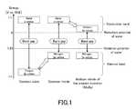
- FIG. 1is a conceptual diagram illustrating the energy levels of the niobium nitride of the present invention and conventional semiconductor materials.
- FIG. 2shows TG-DTA (Thermogravimetry-Differential Thermal Analysis) data of pentakis(dimethylamino)niobium, which is an example of a starting material used in a method for producing a niobium nitride according to a first embodiment of the present invention.
- TG-DTAThermogravimetry-Differential Thermal Analysis
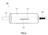
- FIG. 3is a schematic diagram showing an example of an apparatus for carrying out the method for producing a niobium nitride according to the first embodiment of the present invention.
- FIG. 4is a diagram illustrating a Nb 3 N 5 synthesis mechanism in a method for producing Nb 3 N 5 according to a second embodiment of the present invention.
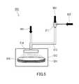
- FIG. 5is a schematic diagram showing an example of an apparatus for carrying out a method for producing a niobium nitride-containing film according to a third embodiment of the present invention.
- FIG. 6is a diagram illustrating a Nb 3 N 5 -containing film synthesis mechanism in a method for producing a Nb 3 N 5 -containing film according to a fourth embodiment of the present invention.
- FIG. 7is a diagram of the density of states distribution of Nb 3 N 5 .
- FIG. 8is a schematic diagram showing an example of a hydrogen generation device according to a sixth embodiment of the present invention.
- FIG. 9is a schematic cross-sectional diagram showing another example of the hydrogen generation device according to the sixth embodiment of the present invention.
- FIG. 10is a schematic cross-sectional diagram showing still another example of the hydrogen generation device according to the sixth embodiment of the present invention.
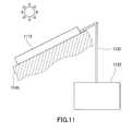
- FIG. 11is a schematic diagram showing an example of an energy system according to a seventh embodiment of the present invention.
- FIG. 12is a schematic diagram showing a more specific example of the energy system according to the seventh embodiment of the present invention.
- FIG. 13shows an X-ray photoelectron spectrum of Nb 3 N 5 according to Example 1-1 of the present invention.
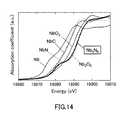
- FIG. 14shows an X-ray absorption near-edge structure (XANES) spectrum of Nb 3 N 5 according to Example 1-1 of the present invention.
- FIG. 15shows an ultraviolet-visible absorption spectrum of a Nb 3 N 5 -containing film according to Example 1-2 of the present invention.
- FIG. 16shows a time course of the amount of hydrogen generated using Nb 3 N 5 according to Example 1-3 of the present invention.
- FIG. 17shows a time course of the amount of oxygen generated using Nb 3 N 5 according to Example 1-4 of the present invention.
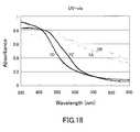
- FIG. 18shows ultraviolet-visible absorption spectra of films 1 A to 1 D according to Example 2-1 of the present invention.
- FIG. 19shows X-ray photoelectron spectra of Nb 3d in the films 1 A to 1 D according to Example 2-1.
- a material used as a photocatalystneeds to be a semiconductor material capable of absorbing relatively long wavelength visible light (having a narrow band gap width), having band edges (the level of the top of the valence band and the level of the bottom of the conduction band) located at levels between which the oxidation potential and reduction potential of water are present, and being stable in an aqueous solution under light irradiation.
- the semiconductor material with a band gap of 700 nmachieves a hydrogen generation efficiency of about 20% at most.
- the installation areanaturally must be increased to generate a required amount of hydrogen.
- the increase in the installation areanot only causes an increase in cost but also makes it difficult to install the device, unlike a solar cell, in a place with a limited area, such as the roof of a detached house.
- the estimated power generation efficiency that a simple type (not a tandem type) Si-based solar cell can achieveis about 20%.
- a semiconductor material with a band gap of 700 nm or moreneeds to be used to obtain an efficiency equal to or higher than that of the solar cell.
- the water decomposition voltageis about 1.23 V
- a semiconductor material with a band gap smaller than 1.23 V (1010 nm or more in terms of wavelength)cannot be used to decompose water in principle. Therefore, it is desired to find a semiconductor material having a band gap width of 1.23 to 1.77 eV (700 nm to 1010 nm in terms of wavelength, the same applies hereinafter).
- the valence band of a common oxidemainly consists of oxygen 2 p orbitals, and the level of the top of the valence band of the oxide is usually located at about +3V (relative to NHE) (left of FIG. 1 ).
- the valence band of a nitridemainly consists of nitrogen 2p orbitals. Therefore, the level of the top of the valence band of the nitride is usually located on the negative side of that of the top of the valence band of the oxide (center of FIG. 1 ). Therefore, as disclosed in Patent Literature 3, the use of a nitride makes it possible to obtain a semiconductor material having a smaller band gap than a material obtained using an oxide.
- Tantalum nitrideis one of the nitride semiconductor materials which are reported to have a photocatalytic function of decomposing water to generate hydrogen and can absorb the longest wavelength light among these materials, but the wavelength of the light that Ta 3 N 5 can absorb is about 600 nm at most. This is smaller than the wavelength of 700 nm, at which the efficiency equal to or higher than that of a solar cell can be obtained.
- a niobium nitride Nb 3 N 5 obtained by substituting all the Ta sites of Ta 3 N 5 by Nbis a semiconductor material having a band gap width of a value between 1.23 and 1.77 eV (700 nm to 1010 nm).
- Nb 4d orbitals that are the primary components of the bottom of the conduction band of Nb 3 N 5are located at a level on the electrochemically positive side of the Ta 5d orbitals that are the primary components of the bottom of the conduction band of Ta 3 N 5 (right of FIG. 1 ).
- the calculated band gap width of Ta 3 N 5was 1.1 eV, while the calculated band gap width of Nb 3 N 5 was 0.8 eV, as shown in Table 1.
- the calculated band gap widthis usually estimated to be smaller than the actual band gap width.
- the comparative evaluation of the band gap widthscan be made with high accuracy, and the orbital components that constitute respective bands (such as the valence band and the conduction band) can also be determined with high accuracy.
- the calculated value of the band gap width of Ta 3 N 5is underestimated to be 52% of the measured value thereof.
- the actual band gap width of Nb 3 N 5 of the present inventionis calculated by applying this ratio to the calculated value of the band gap width of 0.8 eV using the following formula 1.
- the band gap width of Nb 3 N 5is considered to be about 1.5 eV. This means that Nb 3 N 5 has a capacity enough to absorb light having a wavelength of 700 nm or more.
- niobium in the niobium nitrideexhibits the properties of a semiconductor with a band gap when niobium has a valence of +5, which is the highest valence of niobium, and that niobium having a lower valence than the highest valence has a higher electron density in the conduction band, and as a result, it has no apparent band gap. Therefore, it is preferable that niobium in the niobium nitride of the present invention have a valence of substantially +5 (preferably, a valence of +4.8 to +5).
- the conduction bandmainly consists of Nb 4d orbitals. Therefore, it is desirable that the niobium has a valence of +5, in which no electrons are present in the 4d orbitals.
- the present inventorshave found, from the first-principles calculation, that a niobium nitride in which niobium has a valence of 3 exhibits metallic conductivity and has no band gap because electrons are present in the Nb 4d orbitals of the conduction band.
- niobiummay sometimes have a valence of about +4.8 due to unavoidable defects in manufacture, and the like.
- the defectsact as a recombination center of photoexcited carriers and slightly decrease the excitation efficiency and mobility of carriers, but do not have a significant influence on the semiconductor properties. Therefore, in the present invention, such a decrease in the valence of niobium due to unavoidable defects in manufacture is acceptable as long as niobium has a valence of about +4.8 or higher.
- the phrase “niobium has a valence of substantially +5”means that niobium having a valence of about +5 is acceptable as long as that valence value does not have a significant influence on the semiconductor properties, that is, niobium preferably has a valence of +4.8 to +5.
- a first aspect of the present inventionhas been found as a result of the above studies and provides a niobium nitride which has a composition represented by the composition formula Nb 3 N 5 and in which a constituent element Nb has a valence of substantially +5.
- the niobium nitride according to the first aspectis a novel substance, and can be used as a semiconductor material capable of absorbing longer wavelength light (having a smaller band gap), having band edges at levels between which the oxidation-reduction potential of water is present, and having high stability in water under light irradiation. That is, the first aspect of the present invention can provide a semiconductor material having better optical semiconductor properties for obtaining hydrogen and oxygen through decomposition of water than conventional semiconductor materials (having a smaller band gap and a higher sunlight utilization efficiency than conventional semiconductor materials).
- the present inventorshave also provided a method for producing the niobium nitride according to the first aspect and a semiconductor containing such a substance.
- the present inventorshave further provided a film containing the niobium nitride according to the first aspect and a method for producing the film.
- the present inventorshave further provided a semiconductor device, a photocatalyst, a hydrogen generation device, and an energy system each utilizing such a semiconductor or film.
- a second aspect of the present inventionprovides a semiconductor containing the niobium nitride according to the first aspect. Since the semiconductor according to the second aspect contains the niobium nitride according to the first aspect, it can absorb longer wavelength light (has a smaller band gap), has band edges at levels between which the oxidation-reduction potential of water is present, and has high stability in water under light irradiation.
- a third aspect of the present inventionprovides a semiconductor as set forth in the second aspect, wherein the semiconductor is an optical semiconductor.
- the semiconductor according to the third aspectnot only can be used in water but also can achieve a higher sunlight utilization efficiency than conventional optical semiconductors.
- the “optical semiconductor” in the third aspect of the present inventionis defined as a material not only having an electric conductivity within the range of electric conductivity values of semiconductors but also having a band structure in which the conduction band is substantially empty of electrons.
- a fourth aspect of the present inventionprovides a method for producing a niobium nitride, including the step of nitriding an organic niobium compound by reacting the organic niobium compound with a nitrogen compound gas.
- the production method according to the fourth aspectmakes it possible to synthesize the niobium nitride according to the first aspect.
- a fifth aspect of the present inventionprovides a method for producing a niobium nitride as set forth in the fourth aspect, wherein the organic niobium compound contains a compound represented by the composition formula Nb(NR 2 ) 5 , where R is an alkyl group having 1 to 3 carbon atoms.
- the production method according to the fifth aspectmakes it easier to synthesize the niobium nitride according to the first aspect.
- a sixth aspect of the present inventionprovides a method for producing a niobium nitride as set forth in the fifth aspect, wherein the organic niobium compound contains pentakis(dimethylamino)niobium (Nb(N(CH 3 ) 2 ) 5 ).
- the production method according to the sixth aspectmakes it easier to synthesize the niobium nitride according to the first aspect.
- a seventh aspect of the present inventionprovides a method for producing a niobium nitride as set forth in any one of the fourth to sixth aspects, wherein a reaction temperature in the nitriding step is equal to or higher than a nitridation onset temperature of the organic niobium compound and is lower than a reduction onset temperature of Nb.
- the production method according to the seventh aspectmakes it possible to nitride the organic niobium compound while preventing reduction of niobium, and thus makes it easier to synthesize the niobium nitride according to the first aspect.
- a eighth aspect of the present inventionprovides a method for producing a niobium nitride as set forth in the seventh aspect, wherein the organic niobium compound contains pentakis(dimethylamino)niobium (Nb(N(CH 3 ) 2 ) 5 ), and the reaction temperature in the nitriding step is 120° C. to 250° C.
- the production method according to the eighth aspectmakes it possible, when the organic niobium compound contains pentakis(dimethylamino)niobium, to nitride pentakis(dimethylamino)niobium while preventing reduction of niobium, and thus makes it easier to synthesize the niobium nitride according to the first aspect.
- a ninth aspect of the present inventionprovides a method for producing a niobium nitride as set forth in any one of the fourth to eighth aspects, wherein a concentration of water and oxygen contained in the nitrogen compound gas is 10 ppm by volume or less.
- Some of the organic niobium compounds used as starting materialsare highly reactive with water and oxygen. Therefore, a high content of water and oxygen in the synthesis system may cause oxidation of the organic niobium compound during the synthesis process.
- the production method according to the ninth aspectmakes it possible to inhibit oxidation of the organic niobium compound during the synthesis process, and thus makes it easier to synthesize the niobium nitride according to the first aspect.
- a tenth aspect of the present inventionprovides a method for producing a niobium nitride as set forth in any one of the fourth to ninth aspects, wherein a flow rate of the nitrogen compound gas used in the nitriding step is 0.10 m minute ⁇ 1 to 10.0 m minute ⁇ 1 as a linear flow rate.
- the production method according to the tenth aspectmakes it easier to synthesize the niobium nitride according to the first aspect.
- An eleventh aspect of the present inventionprovides a method for producing a niobium nitride as set forth in any one of the fourth to tenth aspects, wherein the nitrogen compound gas used in the nitriding step contains at least ammonia.
- the production method according to the eleventh aspectmakes it easier to synthesize the niobium nitride according to the first aspect.
- a twelfth aspect of the present inventionprovides a method for producing a niobium nitride as set forth in the fourth aspect, wherein the organic niobium compound contains a compound represented by the composition formula R 1 N ⁇ Nb(NR 2 R 3 ) 3 , where R 1 , R 2 and R 3 are each independently a hydrocarbon group, and the nitrogen compound gas contains ammonia.
- the production method according to the twelfth aspectmakes it easier to synthesize the niobium nitride according to the first aspect.
- a thirteenth aspect of the present inventionprovides a method for producing a niobium nitride as set forth in the twelfth aspect, wherein a reaction temperature in the nitriding step is equal to or higher than a nitridation onset temperature of the organic niobium compound and is lower than a reduction onset temperature of Nb.
- the production method according to the thirteenth aspectmakes it easier to synthesize the niobium nitride according to the first aspect.
- a fourteenth aspect of the present inventionprovides a method for producing a niobium nitride as set forth in the twelfth aspect or the thirteenth aspect, wherein R 1 is a tertiary butyl group (—C(CH 3 ) 3 ), and R 2 and R 3 are each independently a straight-chain alkyl group (n-C n H 2n+1 , where n is an integer of 1 or more). Since R 1 is a tertiary butyl group (—C(CH 3 ) 3 ), the resulting organic niobium compound as a raw material is a liquid, thus is easy to handle, and easily undergoes a homogeneous reaction, and further the reduction onset temperature of Nb is increased.
- R 2 and R 3are each a straight-chain alkyl group, the reduction onset temperature of Nb is increased. Therefore, the production method according to the fourteenth aspect makes it easier to synthesize the niobium nitride according to the first aspect.
- a fifteenth aspect of the present inventionprovides a semiconductor device including the semiconductor according to the second aspect or the third aspect. Since the semiconductor device according to the fifteenth aspect includes the semiconductor according to the second aspect or the third aspect, it can be used as a device having a high sunlight utilization efficiency and being usable in water.
- a sixteenth aspect of the present inventionprovides a photocatalyst consisting of the semiconductor according to the third aspect. Since the photocatalyst according to the sixteenth aspect consists of the semiconductor serving as an optical semiconductor according to the third aspect, it not only can be used in water but also can achieve a higher sunlight utilization efficiency than conventional photocatalysts.
- a seventeenth aspect of the present inventionprovides a hydrogen generation device including: the photocatalyst according to the sixteenth aspect; an aqueous solution containing an electrolyte and being in contact with the photocatalyst; and a container containing the photocatalyst and the aqueous solution, wherein hydrogen is generated through decomposition of water in the aqueous solution by irradiation of the photocatalyst with light.
- the hydrogen generation device according to the seventeenth aspectcan achieve more efficient generation of hydrogen than conventional devices.
- An eighteenth aspect of the present inventionprovides an energy system including: the hydrogen generation device according to the seventeenth aspect; a fuel cell; and a line for supplying the hydrogen generated in the hydrogen generation device to the fuel cell.
- the energy system according to the eighteenth aspectcan achieve more efficient generation of energy than conventional systems.
- a nineteenth aspect of the present inventionprovides a niobium nitride-containing film containing a niobium nitride which has a composition represented by the composition formula Nb 3 N 5 and in which a constituent element Nb has a valence of substantially +5.
- the niobium nitride-containing film according to the nineteenth aspectcontains a niobium nitride which has a composition represented by the composition formula Nb 3 N 5 and in which a constituent element Nb has a valence of substantially +5, like the niobium nitride according to the first aspect.
- the niobium nitride-containing film according to the nineteenth aspectcan absorb longer wavelength light (has a smaller band gap), has band edges at levels between which the oxidation-reduction potential of water is present, and has high stability in water under light irradiation.
- a twentieth aspect of the present inventionprovides a method for producing a niobium nitride-containing film containing a niobium nitride which has a composition represented by the composition formula Nb 3 N 5 and in which a constituent element Nb has a valence of substantially +5, the method including the steps of (I) vaporizing an organic niobium compound; and (II) bringing the vaporized organic niobium compound and a nitrogen compound gas into contact with a heated substrate.
- the production method according to the twentieth aspectmakes it possible to produce the niobium nitride-containing film according to the nineteenth aspect.
- a twenty-first aspect of the present inventionprovides a method for producing a niobium nitride-containing film as set forth in the twentieth aspect, wherein the organic niobium compound contains a compound represented by the composition formula Nb(NR 2 ) 5 , where R is an alkyl group having 1 to 3 carbon atoms, and the nitrogen compound gas contains ammonia.
- the production method according to the twenty-first aspectmakes it easier to produce the niobium nitride-containing film according to the nineteenth aspect.
- a twenty-second aspect of the present inventionprovides a method for producing a niobium nitride-containing film as set forth in the twenty-first aspect, wherein in the step (II), the substrate is heated to a temperature that is equal to or higher than a nitridation onset temperature of the organic niobium compound and is lower than a reduction onset temperature of Nb.
- the production method according to the twenty-second aspectmakes it easier to produce the niobium nitride-containing film according to the nineteenth aspect.
- a twenty-third aspect of the present inventionprovides a method for producing a niobium nitride-containing film as set forth in the twentieth aspect or the twenty-first aspect, wherein the organic niobium compound contains pentakis(dimethylamino)niobium (Nb(N(CH 3 ) 2 ) 5 ).
- the production method according to the twenty-third aspectmakes it easier to produce the niobium nitride-containing film according to the nineteenth aspect.
- a twenty-fourth aspect of the present inventionprovides a method for producing a niobium nitride-containing film as set forth in the twentieth aspect, wherein the organic niobium compound contains a compound represented by the composition formula R 1 N ⁇ Nb(NR 2 R 3 ) 3 , where R 1 , R 2 and R 3 are each independently a hydrocarbon group, and the nitrogen compound gas contains ammonia.
- the production method according to the twenty-fourth aspectmakes it easier to produce the niobium nitride-containing film according to the nineteenth aspect.
- a twenty-fifth aspect of the present inventionprovides a method for producing a niobium nitride-containing film as set forth in the twenty-fourth aspect, wherein in the step (II), the substrate is heated to a temperature that is equal to or higher than a nitridation onset temperature of the organic niobium compound and is lower than a reduction onset temperature of Nb.
- the production method according to the twenty-fifth aspectmakes it easier to produce the niobium nitride-containing film according to the nineteenth aspect.
- a twenty-sixth aspect of the present inventionprovides a method for producing a niobium nitride-containing film as set forth in the twenty-fourth aspect or the twenty-fifth aspect, wherein R 1 is a tertiary butyl group (—C(CH 3 ) 3 ), and R 2 and R 3 are each independently a straight-chain alkyl group (n-C n H 2n+1 , where n is an integer of 1 or more).
- the production method according to the twenty-sixth aspectmakes it easier to produce the niobium nitride-containing film according to the nineteenth aspect.
- a twenty-seventh aspect of the present inventionprovides a semiconductor device including the niobium nitride-containing film according to the nineteenth aspect. Since the semiconductor device according to the twenty-seventh aspect includes the niobium nitride-containing film according to the nineteenth aspect, it can be used as a device having a high sunlight utilization efficiency and being usable in water.
- a twenty-eighth aspect of the present inventionprovides a photocatalyst consisting of the niobium nitride-containing film according to the nineteenth aspect. Since the photocatalyst according to the twenty-eighth aspect consists of the niobium nitride-containing film according to the nineteenth aspect, it not only can be used in water but also can achieve a higher sunlight utilization efficiency than conventional photocatalysts.
- a twenty-ninth aspect of the present inventionprovides a hydrogen generation device including: the photocatalyst according to the twenty-eighth aspect; an aqueous solution containing an electrolyte and being in contact with the photocatalyst; and a container containing the photocatalyst and the aqueous solution, wherein hydrogen is generated through decomposition of water in the aqueous solution by irradiation of the photocatalyst with light.
- the hydrogen generation device according to the twenty-ninth aspectcan achieve more efficient generation of hydrogen than conventional devices.
- a thirtieth aspect of the present inventionprovides an energy system including: the hydrogen generation device according to the twenty-ninth aspect; a fuel cell; and a line for supplying the hydrogen generated in the hydrogen generation device to the fuel cell.
- the energy system according to the thirtieth aspectcan achieve more efficient generation of energy than conventional systems.
- a niobium nitridewhich can be used as a semiconductor material, which has a composition represented by the composition formula Nb 3 N 5 , and in which the constituent element Nb has a valence of substantially +5 and a method for producing the niobium nitride, embodiments of a niobium nitride-containing film containing the niobium nitride and a method for producing the niobium nitride-containing film, and further embodiments of a device, etc. utilizing the niobium nitride or the niobium nitride-containing film are described with reference to drawings and a table. The following embodiments are merely examples, and the present invention is not limited to the following embodiments.
- a niobium nitride according to a first embodiment of the present inventionhas a composition represented by the composition formula Nb 3 N 5 , and a constituent element Nb has a valence of substantially +5.
- This niobium nitrideis synthesized by the following method.
- the niobium nitride of the present embodimentcan be synthesized by a method including the nitriding step of nitriding an organic niobium compound by reacting the organic niobium compound with a nitrogen compound gas.
- the organic niobium compounda compound having a composition represented by the composition formula Nb(NR 2 ) 5 , where R is an alkyl group having 1 to 3 carbon atoms, preferably 1 to 2 carbon atoms, is suitably used.
- Ris an alkyl group having 1 to 3 carbon atoms, preferably 1 to 2 carbon atoms
- pentakis(dimethylamino)niobium (Nb(N(CH 3 ) 2 ) 5 )is particularly preferred.
- the organic niobium compound as the starting materialcontains Nb(NR 2 ) 5 , and more preferably it consists of Nb(NR 2 ) 5 .
- nitrogen compound gasfor example, ammonia, nitrogen, hydrazine, or the like can be used. Among these, a nitrogen compound gas containing at least ammonia is preferably used.
- the nitrogen compound gasacts as a nitriding reagent but it also has properties as a reducing agent.
- synthesis of a nitride by reaction of an inorganic niobium compound with a nitrogen compound gasrequires a temperature of at least 450° C. or higher.
- niobiumis reduced due to the properties of the nitrogen compound gas as a reducing agent, and NbN (Nb has a valence of +3) is synthesized as a niobium nitride.
- an organic niobium compound which is more reactive with the nitrogen compound gas than an inorganic niobium compoundis used as a starting material.
- the nitridation reactionis allowed to occur in a lower temperature range. That is, in the method of the present embodiment, it is possible to set the reaction temperature in the nitriding step to a temperature that is equal to or higher than a nitridation onset temperature of the organic niobium compound used as a starting material and is lower than a reduction onset temperature of Nb.
- the organic niobium compound used as the starting materialcontains pentakis(dimethylamino)niobium Nb(N(CH 3 ) 2 ) 5 is described as an example.
- FIG. 2shows TG-DTA data of pentakis(dimethylamino)niobium in an ammonia atmosphere.
- the temperature required for the onset of the nitridation reaction of pentakis(dimethylamino)niobiumis at least 120° C.
- the reaction temperature in the nitriding stepis lower than the reduction onset temperature of Nb. Therefore, in the case where pentakis(dimethylamino)niobium is used, it is possible to nitride pentakis(dimethylamino)niobium while preventing reduction of niobium by reacting pentakis(dimethylamino)niobium with a nitrogen compound gas at a temperature in the range of 120° C.
- the nitrogen compound gascan nitride the niobium compound without reducing it.
- the linear flow rate of the nitrogen compound gasis, for example, 0.10 m minute ⁇ 1 to 10.0 m minute ⁇ 1 .
- the organic niobium compounds used as starting materialsare highly reactive with water and oxygen.
- the reactivity of pentakis(dimethylamino)niobium with water and oxygenis very high. Therefore, water and oxygen contained in the synthesis system may cause oxidation of the organic niobium compound during the synthesis process. This needs to be avoided during the synthesis of Nb 3 N 5 . Therefore, the concentration of water and oxygen contained in the nitrogen compound gas and in an inert gas used for purging during the synthesis process as needed is desirably 10 ppm by volume or less, and more desirably 1 ppm by volume or less.
- the inert gas usedmay be not only a so-called rare gas such as He, Ne, Ar, Kr, or Xe but also nitrogen gas or the like.
- the nitriding stepcan be carried out using, for example, an apparatus 100 as shown in FIG. 3 .
- the apparatus 100includes a tube furnace 111 , a tube 112 penetrating the tube furnace 111 , and a boat 113 placed in the tube 112 .
- Nb 3 N 5(Nb 3 N 5 powder) can be synthesized by heating a raw material 101 set in the boat 113 in the tube 112 , in a gas flow 102 containing a nitrogen compound gas flowing through the tube 112 .
- a material in which the main component of a complete nitrideis not NbN or the like but Nb 3 N 5 (Nb 3 N 5 -containing material) can be synthesized.
- any tube and any boatmay be used as the tube 112 and the boat 113 in the tube furnace 111 as long as they withstand the temperatures at which they are used and the environments in which they are used.
- alumina and quartzare suitably used.
- the desired niobium nitridewhich has a composition represented by the composition formula Nb 3 N 5 and in which the constituent element Nb has a valence of substantially +5, can be obtained by the method described above.
- the production method of the present embodimentincludes the step of heating an organic niobium compound containing a compound represented by the composition formula R 1 N ⁇ Nb(NR 2 R 3 ) 3 , where R 1 , R 2 and R 3 are each independently a hydrocarbon group, in an atmosphere containing ammonia.
- This stepcan be carried out using, for example, the apparatus 100 as shown in FIG. 3 , as in the first embodiment.
- the organic niobium compound as the starting materialcontains R 1 N ⁇ Nb(NR 2 R 3 ) 3 , and more preferably it consists of R 1 N ⁇ Nb(NR 2 R 3 ) 3 .
- the case where the organic niobium compound consists of R 1 N ⁇ Nb(NR 2 R 3 ) 3is described as an example.
- Nb 3 N 5(Nb 3 N 5 powder) can be synthesized by heating a raw material (R 1 N ⁇ Nb(NR 2 R 3 ) 3 ) 101 set in the boat 113 in the tube 112 , in the gas flow 102 containing ammonia flowing through the tube 112 .
- a material in which the main component of a complete nitride is not NbN or the like but Nb 3 N 5 (Nb 3 N 5 -containing material)can be synthesized.
- the raw material R 1 N ⁇ Nb(NR 2 R 3 ) 3be heated at a temperature that is equal to or higher than a nitridation onset temperature of the R 1 N ⁇ Nb(NR 2 R 3 ) 3 and is lower than a reduction onset temperature of Nb. Heating of the raw material in this temperature range makes it possible to synthesize a material in which the main component of a complete nitride is not NbN or the like but Nb 3 N 5 , and thus makes it easier to synthesize a Nb 3 N 5 -containing material (Nb 3 N 5 powder).
- the reduction onset temperature of Nbcan be determined by TG-DTA measurement or the like.
- Nb 3 N 5 production method of the present inventionit is possible to synthesize Nb 3 N 5 even if the temperature for heating the raw material R 1 N ⁇ Nb(NR 2 R 3 ) 3 is higher than the reduction onset temperature of Nb of the R 1 N ⁇ Nb(NR 2 R 3 ) 3 .
- the content of components other than Nb 3 N 5such as NbN, tends to be higher than that in a compound obtained by heating R 1 N ⁇ Nb(NR 2 R 3 ) 3 at a temperature lower than the reduction onset temperature of Nb.
- R 1 N ⁇ Nb(NR 2 R 3 ) 3used as the starting material, R 1 , R 2 , and R 3 are each independently a hydrocarbon group. Therefore, self-condensation reaction is inhibited in the R 1 N ⁇ Nb(NR 2 R 3 ) 3 .
- R 1a branched-chain hydrocarbon group is suitable because the resulting material is a liquid and thus is easy to handle and easily undergoes a homogeneous reaction, and further the reduction onset temperature of Nb is increased.
- a tertiary butyl group (—C(CH 3 ) 3 )is suitable.
- R 2 and R 3straight-chain hydrocarbon groups are suitable because the reduction onset temperature of Nb is increased.
- Straight-chain alkyl groups(n-C n H 2n+1 , where n is an integer of 1 or more) like —CH 3 and C 2 H 5 are suitable. Since a too long carbon chain causes a decrease in the reduction onset temperature of Nb, the carbon number is preferably 3 or less (n ⁇ 3). Since the raw material in which R 1 is a tertiary butyl group (—C(CH 3 ) 3 ), and R 2 and R 3 are each independently a straight-chain alkyl group (n-C n H 2n+1 , where n is an integer of 1 or more) has high heat resistance, it can be synthesized at higher temperatures. As a result, highly crystalline Nb 3 N 5 having much better optical semiconductor properties can be synthesized more easily. It should be noted, however, that the starting material used in the present embodiment is highly reactive with oxygen and water.
- the content of oxygen and water in the starting materialis desirably 1 mol ppm or less of the total amount of the starting material, and more desirably 0.1 mol ppm or less.
- the inert gas usedmay be not only a so-called rare gas such as He, Ne, Ar, Kr, or Xe but also nitrogen gas or the like. It is desirable to use a gas having a low content of oxygen and water. Therefore, the content of oxygen and water in the inert gas is desirably 10 ppm by volume or less, and more desirably 1 ppm by volume or less.
- Nb 3 N 5 synthesis mechanism in the production method of the present embodimentis described with reference to FIG. 4 .
- tertiary-butylimino tris-(ethylmethylamino)niobium(tBuN ⁇ Nb(NEtMe) 3 )
- R 1is a tertiary butyl group
- R 2is an ethyl group
- R 3is a methyl group
- a compound produced by adding ammonia (NH 3 ) to this raw material (R 1 N ⁇ Nb(NR 2 R 3 ) 3 ) 101acts as an initiator and causes addition polymerization of R 1 N ⁇ Nb(NR 2 R 3 ) 3 .
- Nb 3 N 5 powderis obtained. Since the production method of the present embodiment has such a reaction scheme, much less NbN is produced compared to complete nitridation of Nb 2 O 5 with ammonia.
- the production method of the present embodimentmakes it possible to synthesize not NbN but Nb 3 N 5 as a complete nitride of Nb.
- Nb 3 N 5having better optical semiconductor properties for generation of hydrogen and oxygen by decomposition of water than conventional semiconductor materials (Nb 3 N 5 having a smaller band gap and better sunlight utilization efficiency than conventional semiconductor materials) can be produced easily and inexpensively.
- the production method of the present embodimentincludes the steps of (I) vaporizing an organic niobium compound (for example Nb(NR 2 ) 5 , where R is an alkyl group having 1 to 3 carbon atoms (preferably 1 to 2 carbon atoms); and (II) bringing the vaporized organic niobium compound and a nitrogen compound gas into contact with a heated substrate.
- organic niobium compoundfor example Nb(NR 2 ) 5 , where R is an alkyl group having 1 to 3 carbon atoms (preferably 1 to 2 carbon atoms)
- MOCVDMetal-Organic Chemical Vapor Deposition
- this methodmakes it possible to produce a Nb 3 N 5 -containing film fixed to a substrate by chemical bonding.
- the Nb 3 N 5 -containing film obtained by the method of the present embodimentallows Nb 3 N 5 to exhibit its excellent optical semiconductor properties because the Nb 3 N 5 -containing film is well fixed to the substrate.
- the reaction mechanism between the organic niobium compound and the nitrogen compound gas and the suitable reaction temperature in the above step (II)are the same as in the first embodiment.
- the compound suitably used as the organic niobium compound and the gas suitably used as the nitrogen compound gasare also the same as in the first embodiment.
- the MOCVD apparatus 500includes a vaporizer 511 , an inlet pipe 512 , a reaction chamber 513 , a shower head 514 , and a susceptor 515 .
- the vaporizer 511vaporizes the raw material.
- the reaction chamber 513serves as a chamber into which a source gas obtained by vaporizing the raw material in the vaporizer 511 is supplied to grow a crystal on the treatment surface of a substrate 521 .
- the inlet pipe 512supplies a gas such as a source gas to the reaction chamber 513 from the vaporizer 511 .
- the shower head 514is connected to the end of the inlet pipe 512 . It is placed inside the reaction chamber 513 and injects a source gas, a reactant gas, etc. to the substrate 521 to grow a crystal thereon.
- the susceptor 515supports the substrate 521 on which the crystal is to be grown and heats the substrate 521 .
- a reactant gas 503 containing ammoniais mixed into an inert gas 502 containing the raw material 501 heated (desirably heated at a temperature lower than the reduction onset temperature of Nb) and vaporized in the vaporizer 511 .
- the mixed gasis injected from the shower head 514 to the substrate 521 heated by the susceptor 515 .
- the temperature of the heated substrate 521is preferably in the range of temperatures that are equal to or higher than the nitridation onset temperature of the raw material 501 and lower than the reduction onset temperature of Nb.
- Nb 3 N 5can be deposited in the crystalline form on the substrate 521 so as to form a Nb 3 N 5 -containing film.
- the inert gas 502 used heremay be not only a so-called rare gas such as He, Ne, Ar, Kr, or Xe but also nitrogen gas or the like. It is desirable to use a gas having a low content of oxygen and water. Therefore, the content of oxygen and water in the inert gas is desirably 10 ppm by volume or less, and more desirably 1 ppm by volume or less.
- the pipe wall of the MOCVD apparatus 500be made of stainless steel because water and oxygen are less likely to be adsorbed on or desorbed from stainless steel.
- a solution of the raw material and an organic solventmay be vaporized.
- a nonaqueous solvent capable of dissolving the raw material and having the vaporization properties similar to those of the raw material, such as hydrocarbon,is suitable as the organic solvent.
- ethylcyclohexaneis suitably used.
- a Nb 3 N 5 -containing film having a very low content of NbNcan be produced easily and inexpensively.
- a Nb 3 N 5 -containing film having better optical semiconductor properties for generation of hydrogen and oxygen by decomposition of water than films made of conventional semiconductor materials(a Nb 3 N 5 -containing film having a smaller band gap and better sunlight utilization efficiency than conventional semiconductor materials) can be produced easily and inexpensively.
- the method for producing a Nb 3 N 5 -containing film in the case where the organic niobium compound contains a compound represented by the composition formula R 1 N ⁇ Nb(NR 2 R 3 ) 3 , where R 1 , R 2 and R 3 are each independently a hydrocarbon group and the nitrogen compound gas contains ammonia, in the production method of the third embodiment,is described.
- the organic niobium compoundconsists of R 1 N ⁇ Nb(NR 2 R 3 ) 3 is described.
- the production method of the present embodimentincludes the steps of: (I) vaporizing R 1 N ⁇ Nb(NR 2 R 3 ) 3 , where R 1 , R 2 , and R 3 are each independently a hydrocarbon group); and (II) bringing the vaporized R 1 N ⁇ Nb(NR 2 R 3 ) 3 and ammonia into contact with a heated substrate.
- stepscan be carried out using, for example, the MOCVD apparatus 500 as shown in FIG. 5 described in the third embodiment.
- This methodmakes it possible to produce a Nb 3 N 5 -containing film while suppressing the generation of NbN.
- this methodmakes it possible to produce a Nb 3 N 5 -containing film fixed to a substrate by chemical bonding.
- the Nb 3 N 5 -containing film obtained by the method of the present embodimentallows Nb 3 N 5 to exhibit its excellent optical semiconductor properties because the Nb 3 N 5 -containing film is well fixed to the substrate.
- the substratebe heated to a temperature that is equal to or higher than the nitridation onset temperature of R 1 N ⁇ Nb(NR 2 R 3 ) 3 as a raw material and is lower than the reduction onset temperature of Nb. Heating of the substrate in this range of temperatures makes it possible to synthesize not NbN but Nb 3 N 5 as a complete nitride of Nb. It is preferable that, in the step (I), the raw material be vaporized at a temperature that is lower than the reduction onset temperature of Nb of this raw material.
- R 1 N ⁇ Nb(NR 2 R 3 ) 3 used as the starting materialis the same as that described in the second embodiment. Therefore, detailed description thereof is omitted here.
- the configuration of the MOCVD apparatus 500is as described in the third embodiment.
- the reactant gas 503 containing ammoniais mixed into the inert gas 502 containing the raw material (R 1 N ⁇ Nb(NR 2 R 3 ) 3 ) 501 heated (desirably heated at a temperature lower than the reduction onset temperature of Nb) and vaporized in the vaporizer 511 .
- the mixed gasis injected from the shower head 514 to the substrate 521 heated by the susceptor 515 .
- the substrate 521is heated to a temperature that is equal to or higher than the nitridation onset temperature of the raw material 501 and is lower than the reduction onset temperature of Nb, as described above.
- Nb 3 N 5can be deposited on the substrate 521 so as to form a Nb 3 N 5 -containing film.
- the specific examples of the inert gas 502 used hereinare the same as those of the inert gas used in the second embodiment.
- the pipe wall of the MOCVD apparatus 500be made of stainless steel because water and oxygen are less likely to be adsorbed on or desorbed from stainless steel.
- a solution of the R 1 N ⁇ Nb(NR 2 R 3 ) 3 and an organic solventmay be vaporized.
- a nonaqueous solvent capable of dissolving R 1 N ⁇ Nb(NR 2 R 3 ) 3 and having the vaporization properties similar to those of R 1 N ⁇ Nb(NR 2 R 3 ) 3 , such as hydrocarbonis suitable as the organic solvent.
- ethylcyclohexaneis suitably used.
- a compound produced by adding this raw material (R 1 N ⁇ Nb(NR 2 R 3 ) 3 ) 501 to hydroxyl groups on the surface of the substrate 521acts as an initiator and causes addition polymerization of R 1 N ⁇ Nb(NR 2 R 3 ) 3 .
- NR 2 R 3reacts with ammonia and then is condensation polymerized.
- a Nb 3 N 5 -containing filmis obtained. Since the production method of the present embodiment has such a reaction scheme, much less NbN is produced compared to complete nitridation of Nb 2 O 5 with ammonia.
- a Nb 3 N 5 -containing film having a very low content of NbNcan be produced.
- a Nb 3 N 5 -containing film having better optical semiconductor properties for generation of hydrogen and oxygen by decomposition of water than films made of conventional semiconductor materials(a Nb 3 N 5 -containing film having a smaller band gap and better sunlight utilization efficiency than conventional semiconductor materials) can be produced easily and inexpensively.
- the photocatalyst of the present embodimentconsists of the niobium nitride Nb 3 N 5 described in the first embodiment.
- the niobium nitride Nb 3 N 5 described in the first and second embodimentsis a semiconductor having a band gap and can be used as a photocatalyst.
- the reason for thisis described.
- FIG. 7shows density of states distribution of Nb 3 N 5 obtained by the first-principles band calculation.
- Nb 3 N 5is a semiconductor having a band structure in which the valence band mainly consists of nitrogen 2p orbitals, the conduction band mainly consists of niobium 4 d orbitals, and a band gap exists between these two bands.
- the measured value of the band gap widthis 1.6 eV as described later in Example 1-1. This value is equivalent to the energy of light having a wavelength of 780 nm. That is, when Nb 3 N 5 is irradiated with light having a wavelength of 780 nm or less, electrons in the valence band absorb the light and are excited into the conduction band.
- the excited electronsmove from Nb 3 N 5 to the reactive substrate and the reduction reaction of the reactive substrate can proceed.
- the reactive substrate having such an oxidation-reduction potentialinclude water, proton, oxygen, metal ions such as silver (I) ion and iron (III) ion, and iodide ion.
- holesare generated in the valence band with the photoexcitation of electrons.
- a reactive substratewhen a reactive substrate is present in the vicinity of the surface of Nb 3 N 5 and the oxidation-reduction potential thereof is located at a potential on the negative side of the top of the valence band of Nb 3 N 5 , holes move from Nb 3 N 5 to the reactive substrate and the oxidation reaction of the reactive substrate can proceed.
- the reactive substrate having such an oxidation-reduction potentialinclude water, hydroxide ion, metal ions such as iron (II) ion, iodine ion, and an organic compound.
- IIiron
- the niobium nitride Nb 3 N 5 of the present inventioncan absorb visible light and has band edges at levels between which the oxidation-reduction potential of water is present.
- the niobium nitride of the present inventionhas high stability in an aqueous solution under light irradiation. Therefore, the use of the niobium nitride of the present invention as a photocatalyst makes it possible to obtain a hydrogen generation device in which hydrogen is generated through decomposition of water. Since such a hydrogen generation device using the niobium nitride Nb 3 N 5 as a photocatalyst is very efficient in utilizing sunlight, hydrogen can be generated more efficiently than conventional devices.
- the hydrogen generation device of the present embodimentincludes: a photocatalyst consisting of a semiconductor containing a niobium nitride Nb 3 N 5 ; an aqueous solution containing an electrolyte and being in contact with the photocatalyst; and a container containing the photocatalyt and the aqueous solution.
- a photocatalystconsisting of a semiconductor containing a niobium nitride Nb 3 N 5 ; an aqueous solution containing an electrolyte and being in contact with the photocatalyst; and a container containing the photocatalyt and the aqueous solution.
- the configuration of the hydrogen generation device of the present embodimentis, for example, a configuration in which a photocatalyst consisting of a semiconductor (optical semiconductor) containing the niobium nitride Nb 3 N 5 is suspended or immersed in an aqueous solution containing an electrolyte and the resulting solution is placed in a container.
- a photocatalystconsisting of a semiconductor (optical semiconductor) containing the niobium nitride Nb 3 N 5 is suspended or immersed in an aqueous solution containing an electrolyte and the resulting solution is placed in a container.
- a hydrogen generation device 800 of the present embodimentincludes an aqueous solution containing an electrolyte (electrolytic solution) 810 , in which a photocatalyst consisting of a semiconductor (optical semiconductor) containing the niobium nitride Nb 3 N 5 described in the first and second embodiments is suspended, and a container 811 containing the electrolytic solution 810 .
- This hydrogen generation device 800decomposes water by irradiating the electrolytic solution 810 with light so as to generate hydrogen.
- At least a portion (herein referred to as a light incident portion 812 ) of the container 811is made of a material that transmits light such as sunlight so as to allow light such as sunlight to reach the inside of the container 811 .
- the container 811is further provided with an outlet 814 for discharging hydrogen and oxygen generated in the container 811 and an inlet 813 for supplying water to be decomposed into the container 811 .
- the hydrogen generation device 800further includes a hydrogen separation membrane 815 , an oxygen outlet 816 , and a hydrogen outlet 817 .
- the hydrogen separation membrane 815separates hydrogen from the gas discharged from the outlet 814 .
- the hydrogen thus separatedis discharged from the hydrogen outlet 817 .
- the remaining oxygenis discharged from the oxygen outlet 816 .
- the electrolytic solution 810 placed in the container 811 and containing the photocatalyst suspended thereinis irradiated with sunlight through the light incident portion 812 of the container 811 in the hydrogen generation device 800 .
- electronsare generated in the conduction band of the Nb 3 N 5 -containing material in the electrolytic solution 810 and holes are generated in the valence band thereof.
- the holesthus generated decompose water and causes oxygen to be generated according to the reaction formula (1) below.
- the electronscauses hydrogen to be generated according to the reaction formula (2) below.
- the oxygen and hydrogen thus generatedare discharged from the outlet 814 and separated through the hydrogen separation membrane 815 , and then oxygen is discharged from the oxygen outlet 816 and hydrogen is discharged from the hydrogen outlet 817 , respectively.
- Wateris supplied into the container 811 through the inlet 813 to replenish the water used for decomposition.
- the photocatalyst used in the present embodimentSince the photocatalyst used in the present embodiment has excellent optical semiconductor properties, the probability of recombination of holes and electrons is low. Therefore, in the hydrogen generation device 800 , the quantum efficiency of the hydrogen evolution reaction by light irradiation can be increased. In addition, since the photocatalyst used in the present embodiment has a small band gap, it is also responsive to visible light. As a result, the hydrogen generation device 800 of the present embodiment can generate more hydrogen than devices using conventional optical semiconductor materials.
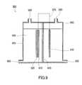
- a hydrogen generation device 900 of FIG. 9includes a container 990 , a photocatalyst electrode 920 , a conductive substrate 910 , and a counter electrode 930 .
- the photocatalyst electrode 920includes the Nb 3 N 5 -containing film described in the third and fourth embodiments.
- the container 990has, in its upper part, two openings 980 for collecting hydrogen and oxygen respectively.
- the container 990has, in its lower part, two openings 980 serving as water inlets.
- An aqueous solution containing an electrolyte (electrolytic solution) 960is placed in the container 990 .
- the container 990has a separator 940 between the photocatalyst electrode 920 and the counter electrode 930 to separate a hydrogen generation chamber from an oxygen generation chamber.
- the separator 940has a function of transmitting ions and separating a gas generated on the photocatalyst electrode 920 side from a gas generated on the counter electrode 930 side.
- a portion (a light incident portion 950 ) of the container 990 that faces the surface of the photocatalyst electrode 920 disposed inside the container 990is made of a material that transmits light such as sunlight.
- the conductive substrate 910 and the counter electrode 930are electrically connected by a conducting wire 970 .
- the counter electroderefers to an electrode that can exchange electrons with the photocatalyst electrode without the electrolytic solution. Accordingly, in the present embodiment, there is no particular limitation on the positional relationship, etc. of the counter electrode 930 with the photocatalyst electrode 920 and the conductive substrate 910 , as long as the counter electrode 930 is connected electrically to the conductive substrate 910 that supports the photocatalyst electrode 920 . It should be noted that since the Nb 3 N 5 -containing film used in the present embodiment is an n-type semiconductor, the counter electrode 930 serves as an electrode that receives electrons from the photocatalyst electrode 920 without the electrolytic solution 960 .
- the photocatalyst electrode 920is a semiconductor having a band gap, it usually has a lower conductivity than metals. In addition, recombination of electrons and holes needs to be prevented as much as possible. Therefore, it is preferable to reduce the thickness of the photocatalyst electrode 920 .
- the photocatalyst electrode 920is formed as a thin film (with a thickness of about 50 to 500 nm) on the conductive substrate 910 . Furthermore, it is preferable to increase the surface area of the photocatalyst electrode 920 to increase the light absorption efficiency.
- the portion of the conductive substrate 910 that is not covered with the photocatalyst electrode 920be covered, for example, with an insulating material such as resin. This covering prevents the conductive substrate 910 from being dissolved in the electrolytic solution 960 .
- the counter electrode 930It is preferable to use a material with a low overvoltage for the counter electrode 930 .
- a metal catalystsuch as Pt, Au, Ag, Fe, or Ni as the counter electrode 930 because the use thereof increases its activity.
- Any electrolytic solutioncan be used for the electrolytic solution 960 as long as it is a solution containing water. An acidic, neutral or basic solution can be used.
- FIG. 10Another hydrogen generation device 1000 shown in FIG. 10 also includes the container 990 , the photocatalyst electrode 920 , the conductive substrate 910 , and the counter electrode 930 (in FIG. 10 , the same or similar members are designated by the same reference numerals as in FIG. 9 ).
- the container 990has four openings 980 and contains the electrolytic solution 960 .
- the photocatalyst electrode 920is provided on one surface of the conductive substrate 910 and the counter electrode 930 is provided on the other surface thereof.
- the photocatalyst electrode 920is formed as a thin film (with a thickness of about 50 to 500 nm).
- the photocatalyst electrode 920 and the counter electrode 930are electrically connected by the conductive substrate 910 .
- the inside of the container 990is separated into a photocatalyst electrode 920 side and a counter electrode 930 side by the separator 940 and the conductive substrate 910 to separate a hydrogen generation chamber from an oxygen generation chamber.
- a portion (a light incident portion 950 ) of the container 990 that faces the surface of the photocatalyst electrode 920 disposed inside the container 990is made of a material that transmits light such as sunlight.
- Hydrogen and oxygencan be generated by irradiating the hydrogen generation devices shown in FIG. 9 and FIG. 10 with light (for example, sunlight) through the light incident portion 950 .
- lightfor example, sunlight
- longer wavelength lightcan be absorbed and thus hydrogen can be generated more efficiently.
- the operation of the hydrogen generation device 900 of the present embodimentis described in more detail.
- the photocatalyst electrode 920 disposed in the container 990is irradiated with sunlight through the light incident portion 950 of the container 990 in the hydrogen generation device 900 , electrons are generated in the conduction band and holes are generated in the valence band, respectively, in the portion of the photocatalyst electrode 920 irradiated with light.
- the Nb 3 N 5 -containing film that constitutes the photocatalyst electrode 920is an n-type semiconductor, the potential of the surface of the photocatalyst electrode 920 is higher than the potential of the inside thereof. Therefore, the holes generated at this time move to the surface of the photocatalyst electrode 920 along the band edge of the valence band. Thus, water is decomposed on the surface of the photocatalyst electrode 920 according to the above reaction formula (1), so that oxygen is generated. On the other hand, the electrons move, along the band edge of the conduction band, from the surface near-field region of the photocatalyst electrode 920 to the conductive substrate 910 through the inside of the photocatalyst electrode 920 .
- the oxygen thus generatedis discharged from the opening 980 for collecting oxygen on the photocatalyst electrode 920 side, and the hydrogen thus generated is discharged from the opening 980 for collecting hydrogen on the counter electrode 930 side, respectively.
- Wateris supplied into the container 990 through the opening 980 serving as a water inlet to replenish the water used for decomposition.
- the hydrogen generation devices 900 and 1000 of the present embodimentare each a so-called photoelectrochemical cell using, as an electrode, a Nb 3 N 5 -containing film serving as an optical semiconductor. Therefore, in the hydrogen generation devices 900 and 1000 , efficient charge separation between holes and electrons is achieved, and thus the quantum efficiency of the hydrogen evolution reaction by light irradiation is increased. In addition, since Nb 3 N 5 has a small band gap, it is also responsive to visible light in sunlight. As a result, the hydrogen generation devices 900 and 1000 of the present embodiment can generate more hydrogen than devices using conventional optical semiconductor materials. Moreover, in the hydrogen generation devices 900 and 1000 , hydrogen and oxygen can be generated separately, and thus it is easy to collect hydrogen and oxygen separately.
- the energy system of the present embodimentis a system that uses the photocatalyst described in the fifth embodiment.
- the energy system of the present embodimentis a system in which hydrogen generated through decomposition of water by irradiation of the photocatalyst with light is supplied to a fuel cell and converted into electrical energy.
- the energy system of the present embodimentincludes such a hydrogen generation device as described in the sixth embodiment.
- FIG. 11shows a schematic view of the energy system of the present embodiment that uses sunlight.
- the energy system of the present inventionis not limited to the configuration shown in FIG. 11 .
- the energy system of the present embodimentincludes such a hydrogen generation device 1110 as described in the sixth embodiment, a fuel cell 1120 , and a line 1130 for supplying the hydrogen generated in the hydrogen generation device 1110 to the fuel cell 1120 .
- the hydrogen generation device 1110is installed in a place 1140 filled with sunlight such as on the roof, for example.
- sunlightsuch as on the roof
- the hydrogen obtained in the hydrogen generation device 1110 through decomposition of water caused by the photocatalytic reactionis discharged out of the hydrogen generation device 1110 through the line 1130 so as to be supplied to the fuel cell 1120 .
- the line 1130may be provided, for example, with a hydrogen storage unit for storing hydrogen, a dehumidifier for removing moisture in the hydrogen, a compressor unit when hydrogen is required to be compressed for storage, etc.
- FIG. 12shows a more specific example of the energy system of the present embodiment.
- An energy system 1200 shown in FIG. 12includes a hydrogen generation device 1110 , a hydrogen storage 1210 , a fuel cell 1120 , and a storage battery 1220 .
- the hydrogen storage 1210is connected to the hydrogen generation device 1110 by a first pipe 1230 and stores hydrogen generated in the hydrogen generation device 1110 .
- the hydrogen storage 1210can be composed of, for example, a compressor for compressing hydrogen generated in the hydrogen generation device 1110 and a high-pressure hydrogen tank for storing the hydrogen compressed by the compressor.
- the fuel cell 1120includes a power generator 1121 and a fuel cell controller 1122 for controlling the power generator 1121 .
- the fuel cell 1120is connected to the hydrogen storage 1210 by a second pipe 1240 , and converts the hydrogen stored in the hydrogen storage 1210 into electricity and heat.
- the second pipe 1240is provided with a block valve 1250 .
- a polymer electrolyte fuel cellcan be used as the fuel cell 1120 .
- the positive electrode and the negative electrode of the storage battery 1220respectively are connected electrically to the positive electrode and the negative electrode of the power generator 1121 in the fuel cell 1120 by a first line 1260 and a second line 1270 .
- the storage battery 1220is provided with a capacity meter 1280 for measuring the remaining capacity of the storage battery 1220 .
- a lithium ion batterycan be used as the storage battery 1220 .
- the hydrogen generated by the operation of the hydrogen generation device described in the sixth embodimentis supplied into the hydrogen storage 1210 through the opening 980 for collecting hydrogen (see FIG. 9 and FIG. 10 ) and the first pipe 1230 .
- the block valve 1250is opened according to signals from the fuel cell controller 1122 , so that the hydrogen stored in the hydrogen storage 1210 is supplied to the power generator 1121 of the fuel cell 1120 through the second pipe 1240 .
- the electricity generated in the power generator 1121 of the fuel cell 1120is stored in the storage battery 1220 through the first line 1260 and the second line 1270 .
- the electricity stored in the storage battery 1220is supplied to home and business users through a third line 1290 and a fourth line 1300 .
- the quantum efficiency of the hydrogen evolution reaction by light irradiationcan be increased.
- the energy system 1200 including this hydrogen generation device 1100can supply electric power efficiently.
- Example 1an example in which a compound represented by the composition formula Nb(NR 2 ) 5 was used as an organic niobium compound that is a starting material is described.
- Example 1-1 of the present inventionis specifically described.
- a starting materialpentakis(dimethylamino)niobium (Nb(N(CH 3 ) 2 ) 5 ) powder (1.0 g) was used.
- the starting materialwas maintained at room temperature for 8 hours under a flow of ammonia gas (with a purity of 99.999% or more) at a linear flow rate of 2.2 m minute ⁇ 1 .
- the temperature of the starting materialwas raised to 160° C. at a temperature rise rate of 5° C. minute ⁇ 1 under the ammonia gas flow at a linear flow rate of 2.2 m minute ⁇ 1 , and then maintained at 160° C. for 8 hours.
- Nb 3 N 5was obtained.
- FIG. 13shows the X-ray photoelectron spectrum of the Nb 3 N 5 powder synthesized in this example.
- the X-ray photoelectron spectrumis obtained by observing the kinetic energy of photoelectrons emitted from a sample under X-ray irradiation.
- the peak position of the sampleshifts due to a difference in the chemical state of a target element. Therefore, information about the valence and binding state of the element can be obtained from the shift.
- the higher the valence of the elementis, the more the peak position in the spectrum shifts toward the high binding energy side.
- the higher the electronegativity of an element bonded to the target elementis, the more the peak position shifts toward the high binding energy side.
- the Nb 3d5/2 peakis located at a binding energy of 205.6 eV.
- the Nb 3d5/2 peakis located between the peak of Nb 2 O 5 (where niobium has a valence of +5) as a reference and the peak of NbN (where niobium has a valence of +3).
- the Nb element of Nb 3 N 5is bonded to the N element, while the Nb element of Nb 2 O 5 is bonded to the O element.
- the peak of Nb 2 O 5shifts more toward the high binding energy side than that of Nb 3 N 5 , as described above.
- the above peak position of Nb 3 N 5 in the spectrummeans that Nb species contained in the sample has a valence of +5 and it is bonded to N.
- X-ray absorption fine structure (XAFS) analysis of the Nb 3 N 5 powder produced in this examplewas performed.
- the XAFS spectrumis an absorption spectrum resulting from the excitation of inner shell electrons of a target element that occurs when the element is irradiated with X-rays.
- a region near the absorption edge of the XAFS spectrumis called an X-ray absorption near edge structure (XANES) spectrum.
- the XANES spectrumis sensitive to the valence of a target element, and generally, the higher the valence of the element is, the more the absorption edge position in the spectrum shifts toward the high energy side.
- FIG. 14shows the XANES spectrum of the Nb 3 N 5 produced in this example. It can be seen from FIG.
- the absorption edge of the spectrum of a compound in which Nb has a higher valenceshifts more toward the high energy side.
- the absorption edge of the spectrum of the target Nb 3 N 5almost coincides with that of a niobium oxide (Nb 2 O 5 ) in which Nb species has a valence of +5. This fact also means that Nb species contained in the sample has a valence of +5.
- a Nb 3 N 5 -containing filmwas synthesized using the MOCVD apparatus 500 shown in FIG. 5 .
- An ethylcyclohexane solution of the raw material 501 at 6.76 ⁇ 10 ⁇ 6 Pa ⁇ m 3 s ⁇ 1 (0.04 sccm)was vaporized at 130° C. in the vaporizer 511 .
- the nitrogen gas 502was used as an inert gas.
- the ammonia 503 at 1.69 ⁇ 10 ⁇ 3 Pa ⁇ m 3 s ⁇ 1 (10 sccm)was mixed with a mixed gas at 1.69 ⁇ 10 ⁇ 1 Pa ⁇ m 3 s ⁇ 1 (1000 sccm) containing the source gas (vaporized raw material 501 ) and the nitrogen gas 502 .
- the resulting gas mixturewas injected for 12 hours from the shower head 514 to the substrate 521 (ITO film (with a thickness of 150 nm)/glass substrate) heated at 150° C. by the susceptor 515 .
- the substrate 521ITO film (with a thickness of 150 nm)/glass substrate) heated at 150° C. by the susceptor 515 .
- a Nb 3 N 5 -containing film with a thickness of 140 nmwas obtained.
- FIG. 15shows the ultraviolet-visible absorption spectrum of the Nb 3 N 5 -containing film produced in this example. It was found from FIG. 15 that the resulting material can absorb visible light having a wavelength up to 780 nm. This demonstrated that the above material was a semiconductor with a band gap of 1.6 eV (the following formula 2). This measured value almost coincided with the band gap value (1.5 eV) of Nb 3 N 5 estimated based on the result of the first-principles band calculation.
- Example 1-3 of the present inventionis specifically described.
- Nb 3 N 5 synthesized in Example 1-1was allowed to be loaded with platinum (Pt) as a co-catalyst thereon using the following method.
- Nb 3 N 5was impregnated with hexachloroplatinate (IV) (H 2 PtCl 6 ) that is equivalent to 1 wt % of Nb 3 N 5 in an aqueous solution, followed by drying in a steam bath. Thereafter, it was subjected to a hydrogen reduction treatment at 200° C. for 2 hours. Thus, Pt-loaded Nb 3 N 5 was obtained.
- FIG. 16shows a time course of the amount of hydrogen generated under irradiation of this suspension with visible light having a wavelength of 420 nm to 800 nm.
- the light irradiationwas performed through a cold mirror for blocking light other than the light having a wavelength of 420 nm to 800 nm.
- hydrogenwas generated at a maximum generation rate of 0.24 ⁇ mol hour ⁇ 1 as shown in FIG. 16 . It was confirmed from this that Pt-loaded Nb 3 N 5 had a photocatalytic function for reducing protons in the methanol aqueous solution to hydrogen under irradiation with visible light.
- Nb 3 N5(0.20 g) was suspended in 200 mL of a 10 vol % methanol aqueous solution in the same manner as in Example 1-3. The amount of hydrogen generated in this suspension placed in a dark place was measured. However, even after 7 hours from the start, no hydrogen was detected. This proved that the hydrogen evolution reaction in the suspension in Example 1-3 proceeded by the function of Nb 3 N 5 as a photocatalyst.
- Nb 3 N 5 synthesized in Example 1-1was allowed to be loaded with iridium oxide (IrO 2 ) as a co-catalyst using the following method.
- Nb 3 N 5was suspended in an aqueous solution containing iridium (IV)-oxide dihydrate (IrO 2 .2H 2 O) colloid that is equivalent to 5 wt % of Nb 3 N 5 , so that the iridium (IV)-oxide dihydrate colloid was adsorbed on the surface of the Nb 3 N 5 . Thereafter, it was filtered, washed with water, and then subjected to a calcination treatment at 150° C. in vacuum. Thus, IrO 2 -loaded Nb 3 N 5 was obtained.
- FIG. 17shows a time course of the amount of oxygen generated under irradiation of this suspension with ultraviolet light.
- the light irradiationwas performed using a 450-W high-pressure mercury lamp as the light source.
- oxygenwas generated at a maximum generation rate of 3.1 ⁇ mol hour ⁇ 1 as shown in FIG. 17 .
- Nb 3 N 5had a photocatalytic function for oxidizing water in the silver nitrate aqueous solution to oxygen under irradiation with light.
- Example 2an example in which a compound represented by the composition formula R 1 N ⁇ Nb(NR 2 R 3 ) 3 was used as an organic niobium compound that is a starting material is described.
- tertiary-butylimino tris-(ethylmethylamino)niobium((CH 3 ) 3 CN ⁇ Nb(N(C 2 H 5 )CH 3 ) 3 ) was used.
- the reduction onset temperature of Nb in this raw materialwas determined based on the TG-DTA data thereof. As a result, the reduction temperature of Nb in this raw material was about 303° C.
- a Nb 3 N 5 -containing filmwas synthesized using the MOCVD apparatus 500 shown in FIG. 5 .
- An ethylcyclohexane solution of the raw material 501 at 6.76 ⁇ 10 ⁇ 6 Pa ⁇ m 3 s ⁇ 1 (0.04 sccm)was vaporized at 150° C. in the vaporizer 511 .
- the nitrogen gas 502was used as an inert gas.
- the resulting gas mixturewas injected for 6 hours from the shower head 514 to the substrate 521 (ITO film (with a thickness of 150 nm)/glass substrate) heated at 300° C. by the susceptor 515 .
- a film 1 A(ammonia: 0 sccm)
- a film 1 B(ammonia: 1 sccm)
- a film 1 C(ammonia: 5 sccm)
- a film 1 D(ammonia: 10 sccm) each with a thickness of 200 nm were obtained.
- FIG. 18shows the ultraviolet-visible absorption spectra of the films 1 A to 1 D.
- the absorption edges of 1 A to 1 Dare considered to be about 780 nm from the ultraviolet-visible absorption spectra thereof.
- FIG. 19shows the X-ray photoelectron spectra of Nb 3d in the films 1 A to 1 D and the Nb 3 N 5 powder (referred to as “1P”) synthesized in Example 1-1. It can be seen from FIG. 19 that the peak at 205.6 eV on the low energy side, which is considered to be the peak of Nb 3 N 5 , increases as the amount of ammonia increases (from 1 A to 1 D). As a result, it was confirmed that the films 1 B to 1 D contained Nb 3 N 5 , that is, they were Nb 3 N 5 -containing films.
- the ammonia flow rates during the synthesis of the Nb 3 N 5 -containing filmswere 0 to 1.69 ⁇ 10 ⁇ 3 Pa ⁇ m 3 s ⁇ 1 (0, 1, 5, and 10 sccm). It was confirmed that the Nb 3 N 5 -containing film was also synthesized when the ammonia flow rate was higher than the above rates, although the film forming rate was lower.
- a Nb 3 N 5 powderwas synthesized using the apparatus 100 shown in FIG. 3 .
- the raw material 101was set in the boat 113 in the quartz tube 112 with an inner diameter of 25 mm in the tube furnace 111 .
- the same tertiary-butylimino tris-(ethylmethylamino)niobium ((CH 3 ) 3 CN ⁇ Nb(N(C 2 H 5 )CH 3 ) 3 )was used as in Example 2-1.
- This raw material 101was heated at 300° C. for 4 hours under an ammonia flow at 1.69 ⁇ 10 ⁇ 1 Pa ⁇ m 3 s ⁇ 1 (1000 sccm). Thus, a powder 2 was obtained.
- This powder 2was subjected to elemental analysis, and it was found that the powder 2 consisted only of Nb and N, and the ratio of the number of Nb atoms and that of N atoms (Nb/N) was 3.0/4.9. This result indicated that Nb 3 N 5 was produced.
- the X-ray photoelectron spectrum of the powder 2was compared with the X-ray photoelectron spectrum of the Nb 3 N 5 powder of Example 1-1. As a result, it was confirmed that these data almost coincided with each other. It was thus confirmed that the powder 2 was a Nb 3 N 5 -containing material.
- the ammonia flow rate during the synthesis of the Nb 3 N 5 -containing materialwas 1.69 ⁇ 10 ⁇ 1 Pa ⁇ m 3 s ⁇ 1 (1000 sccm). It was confirmed that the Nb 3 N 5 -containing material was also synthesized when the ammonia flow rate was in the range of 10 sccm to 1000 sccm, although the production rate was low. It was confirmed that the Nb 3 N 5 -containing material was also synthesized when the ammonia flow rate was 1000 sccm or higher, although the production rate was unchanged.
- tertiary-butylimino tris-(diethylamino)niobium((CH 3 ) 3 CN ⁇ Nb(N(C 2 H 5 ) 2 ) 3 ) was used.
- the reduction onset temperature of Nb in this raw materialwas determined based on the TG-DTA data thereof, in the same manner as in Example 2-1. As a result, the reduction onset temperature of Nb in this raw material was about 410° C.
- a Nb 3 N 5 -containing filmwas synthesized using the MOCVD apparatus 500 shown in FIG. 5 .
- An ethylcyclohexane solution of the raw material 501 at 6.76 ⁇ 10 ⁇ 6 Pa ⁇ m 3 s ⁇ 1 (0.04 sccm)was vaporized at 150° C. in the vaporizer 511 .
- the nitrogen gas 502was used as an inert gas.
- the ammonia 503 at 1.69 ⁇ 10 ⁇ 3 Pa ⁇ m 3 s ⁇ 1 (10 sccm)was mixed with a mixed gas at 2.87 ⁇ 10 ⁇ 1 Pa ⁇ m 3 s ⁇ 1 (1700 sccm) containing the source gas (vaporized raw material 501 ) and the nitrogen gas 502 .
- the resulting gas mixturewas injected for 6 hours from the shower head 514 to the substrate 521 (ITO film (with a thickness of 150 nm)/glass substrate) heated at 400° C. by the susceptor 515 .
- a film 3 with a thickness of 300 nmwas obtained.
- Nb 3 dThe X-ray photoelectron spectrum of Nb 3 d in this film 3 was measured. The peak of Nb 3 d was observed at 205.6 eV on the low energy side. It was confirmed from this result that the film 3 was a Nb 3 N 5 -containing film.
- tertiary-butylimino tris-(dimethylamino)niobium((CH 3 ) 3 CN ⁇ Nb(N(CH 3 ) 2 ) 3 ) was used.
- the reduction onset temperature of Nb in this raw materialwas determined based on the TG-DTA data thereof, in the same manner as in Example 2-1. As a result, the reduction onset temperature of Nb in this raw material was about 250° C.
- a Nb 3 N 5 -containing filmwas synthesized using the MOCVD apparatus 500 shown in FIG. 5 .
- An ethylcyclohexane solution of the raw material 501 at 6.76 ⁇ 10 ⁇ 6 Pa ⁇ m 3 s ⁇ 1 (0.04 sccm)was vaporized at 150° C. in the vaporizer 511 .
- the nitrogen gas 502was used as an inert gas.
- the ammonia 503 at 1.69 ⁇ 10 ⁇ 3 Pa ⁇ m 3 s ⁇ 1 (10 sccm)was mixed with a mixed gas at 2.87 ⁇ 10 ⁇ 1 Pa ⁇ m 3 s ⁇ 1 (1700 sccm) containing the source gas (vaporized raw material 501 ) and the nitrogen gas 502 .
- the resulting gas mixturewas injected for 6 hours from the shower head 514 to the substrate 521 (ITO film (with a thickness of 150 nm)/glass substrate) heated at 240° C. by the susceptor 515 .
- a film 4 with a thickness of 500 nmwas obtained.
- the X-ray photoelectron spectrum of Nb 3 d in this film 4was measured.
- the peak of Nb 3 dwas observed at 205.6 eV. It was confirmed from this result that the film 4 was a Nb 3 N 5 -containing film.
- the hydrogen generation device of the present inventionAs an example of the hydrogen generation device of the present invention, a hydrogen generation device having the same configuration as that of the hydrogen generation device 900 shown in FIG. 9 was fabricated. The configuration of the hydrogen generation device of the present embodiment is described with reference to FIG. 9 .
- the hydrogen generation device 900 of Example 2-5included a rectangular glass container 990 with openings in the upper part, a photocatalyst electrode 920 , a conductive substrate 910 , and a counter electrode 930 .
- the glass container 990contained 1 mol L ⁇ 1 of H 2 SO 4 aqueous solution as the electrolytic solution 960 .
- the photocatalyst electrode 920As the photocatalyst electrode 920 , a 1-cm-square electrode, which was fabricated in Example 2-1, in which the 200-nm-thick film 1 D was provided on the substrate 521 (ITO film (with a thickness of 150 nm)/glass substrate) (corresponding to the conductive substrate 910 ), was used.
- the photocatalyst electrode 920was disposed so that the surface thereof faced the light incident surface 950 of the glass container 990 .
- a platinum platewas used as the counter electrode 930 .
- the conductive substrate 910 and the counter electrode 930were electrically connected by the conducting wire 970 .
- the current flowing between the photocatalyst electrode 920 and the counter electrode 930was measured with an ammeter.
- a solar simulator manufactured by SERIC Ltd.was used to apply simulated sunlight.
- the surface of the photocatalyst electrode 920was irradiated with light at an intensity of 1 kW/m 2 through the light incident portion 950 of the hydrogen generation device 900 of Example 2-5.
- the gas generated on the surface of the counter electrode 930was collected for 60 minutes, and the components of the collected gas were analyzed and the amount of the gas generated was measured by gas chromatography.
- the photocurrent flowing between the photocatalyst electrode 920 and the counter electrode 930was measured with an ammeter. The apparent quantum efficiency was calculated using the amount of the gas generated in the counter electrode 930 .
- the Nb 3 N 5 -containing film used in this examplehad optical semiconductor properties for generation of hydrogen and oxygen by decomposition of water under light irradiation.
- the Nb 3 N 5 of the present inventioncan be used as a semiconductor material, high efficient hydrogen generation can be achieved by utilizing sunlight. Hydrogen thus obtained can be used as a fuel for fuel cells, for example.
Landscapes
- Chemical & Material Sciences (AREA)
- Engineering & Computer Science (AREA)
- Organic Chemistry (AREA)
- Materials Engineering (AREA)
- Chemical Kinetics & Catalysis (AREA)
- Manufacturing & Machinery (AREA)
- Ceramic Engineering (AREA)
- Inorganic Chemistry (AREA)
- Structural Engineering (AREA)
- General Chemical & Material Sciences (AREA)
- Electrochemistry (AREA)
- Sustainable Energy (AREA)
- Sustainable Development (AREA)
- Life Sciences & Earth Sciences (AREA)
- Health & Medical Sciences (AREA)
- General Health & Medical Sciences (AREA)
- Physics & Mathematics (AREA)
- Combustion & Propulsion (AREA)
- Thermal Sciences (AREA)
- Crystallography & Structural Chemistry (AREA)
- Metallurgy (AREA)
- Electromagnetism (AREA)
- Toxicology (AREA)
- Catalysts (AREA)
- Chemical Vapour Deposition (AREA)
Abstract
Description
- The present invention relates to a niobium nitride and a method for producing the niobium nitride, a niobium nitride-containing film and a method for producing the niobium nitride-containing film, a semiconductor, a semiconductor device, a photocatalyst suitable for water decomposition reaction, a hydrogen generation device including the photocatalyst, and an energy system including the hydrogen generation device.
- Conventionally, water is decomposed into hydrogen and oxygen by irradiating a semiconductor material serving as a photocatalyst with light.
- For example,
Patent Literature 1 discloses a method in which an n-type semiconductor electrode and a counter electrode are disposed in an electrolytic solution and the surface of the n-type semiconductor electrode is irradiated with light to obtain hydrogen and oxygen from the surfaces of these electrodes.Patent Literature 1 describes the use of a TiO2electrode, a ZnO electrode, or the like as the n-type semiconductor electrode. Patent Literature 2 discloses a gas generator including a metal electrode and a nitride semiconductor electrode that are connected to each other and are disposed in a solvent.Patent Literature 2 describes the use of a nitride of a Group 13 element such as indium, gallium or aluminum for the nitride semiconductor electrode.- These conventional semiconductor electrodes have a problem of low hydrogen generation efficiency in water decomposition reaction by sunlight irradiation. The reason for this is as follows. Semiconductor materials such as TiO2and ZnO can absorb only short wavelength light, that is, light having a wavelength of approximately 400 nm or less. Therefore, only a very small fraction of the total sunlight can be utilized. For example, when TiO2is used, only about 4.7% of sunlight can be utilized. Furthermore, in view of a theoretical loss of the absorbed light due to heat loss, the sunlight utilization efficiency is only about 1.7%.
Patent Literature 3 discloses a photocatalyst containing an orthorhombic tantalum nitride as a semiconductor material capable of absorbing longer wavelength visible light.Patent Literature 3 also reports that tantalum nitride Ta3N5can absorb light having a wavelength of 600 nm or less. However, the light having a wavelength of 600 nm or less accounts for only about 16% of the total sunlight. Furthermore, in view of a theoretical heat loss, the utilization efficiency is only about 6%.Patent Literature 1 JP 51 (1976)-123779 APatent Literature 2 JP 2003-024764 APatent Literature 3 JP 2002-233769 A- In order to decompose water by irradiating a semiconductor material with light, the band edges (the level of the top of the valence band and the level of the bottom of the conduction band) of the semiconductor material need to be located at levels between which the oxidation-reduction potential of water (the level of oxygen evolution and the level of hydrogen evolution) is present. Therefore, the requirements for a semiconductor material that can be practically used for water decomposition are that: the semiconductor material must be able to absorb longer wavelength light (the semiconductor material must have a smaller band gap); the band edges of the semiconductor material must be located at levels between which the oxidation-reduction potential of water is present; and the semiconductor material must be stable in water under light irradiation. However, semiconductor materials that meet all of these requirements have not been found.
- Thus, it is an object of the present invention to provide a substance that can be used as a semiconductor material capable of absorbing longer wavelength light (having a smaller band gap), having band edges at levels between which the oxidation-reduction potential of water is present, and having high stability in water under light irradiation.
- The present invention provides a niobium nitride which has a composition represented by the composition formula Nb3N5and in which the constituent element Nb has a valence of substantially +5.
- The niobium nitride of the present invention is a novel substance, and can be used as a semiconductor material capable of absorbing longer wavelength light (having a smaller band gap), having band edges at levels between which the oxidation-reduction potential of water is present, and having high stability in water under light irradiation.
FIG. 1 is a conceptual diagram illustrating the energy levels of the niobium nitride of the present invention and conventional semiconductor materials.FIG. 2 shows TG-DTA (Thermogravimetry-Differential Thermal Analysis) data of pentakis(dimethylamino)niobium, which is an example of a starting material used in a method for producing a niobium nitride according to a first embodiment of the present invention.FIG. 3 is a schematic diagram showing an example of an apparatus for carrying out the method for producing a niobium nitride according to the first embodiment of the present invention.FIG. 4 is a diagram illustrating a Nb3N5synthesis mechanism in a method for producing Nb3N5according to a second embodiment of the present invention.FIG. 5 is a schematic diagram showing an example of an apparatus for carrying out a method for producing a niobium nitride-containing film according to a third embodiment of the present invention.FIG. 6 is a diagram illustrating a Nb3N5-containing film synthesis mechanism in a method for producing a Nb3N5-containing film according to a fourth embodiment of the present invention.FIG. 7 is a diagram of the density of states distribution of Nb3N5.FIG. 8 is a schematic diagram showing an example of a hydrogen generation device according to a sixth embodiment of the present invention.FIG. 9 is a schematic cross-sectional diagram showing another example of the hydrogen generation device according to the sixth embodiment of the present invention.FIG. 10 is a schematic cross-sectional diagram showing still another example of the hydrogen generation device according to the sixth embodiment of the present invention.FIG. 11 is a schematic diagram showing an example of an energy system according to a seventh embodiment of the present invention.FIG. 12 is a schematic diagram showing a more specific example of the energy system according to the seventh embodiment of the present invention.FIG. 13 shows an X-ray photoelectron spectrum of Nb3N5according to Example 1-1 of the present invention.FIG. 14 shows an X-ray absorption near-edge structure (XANES) spectrum of Nb3N5according to Example 1-1 of the present invention.FIG. 15 shows an ultraviolet-visible absorption spectrum of a Nb3N5-containing film according to Example 1-2 of the present invention.FIG. 16 shows a time course of the amount of hydrogen generated using Nb3N5according to Example 1-3 of the present invention.FIG. 17 shows a time course of the amount of oxygen generated using Nb3N5according to Example 1-4 of the present invention.FIG. 18 shows ultraviolet-visible absorption spectra offilms 1A to1D according to Example 2-1 of the present invention.FIG. 19 shows X-ray photoelectron spectra ofNb 3d in thefilms 1A to1D according to Example 2-1.- In order to decompose water efficiently using sunlight so as to generate hydrogen, a material used as a photocatalyst needs to be a semiconductor material capable of absorbing relatively long wavelength visible light (having a narrow band gap width), having band edges (the level of the top of the valence band and the level of the bottom of the conduction band) located at levels between which the oxidation potential and reduction potential of water are present, and being stable in an aqueous solution under light irradiation.
- How large the band gap should be to achieve a hydrogen generation efficiency comparable to that of a now commonly used Si-based solar cell is discussed below. In the case of a semiconductor material capable of absorbing light having a wavelength of 700 nm or less, about 48% of the total sunlight can be utilized. In view of a theoretical loss of this fraction of light due to heat loss, the hydrogen generation efficiency is about 25%. This is the value obtained on the assumption that the quantum efficiency is 100%. Therefore, if the semiconductor material is incorporated into a device, other losses due to a decrease in the quantum efficiency, reflection and scattering of light on the glass surface, absorption of light by water, etc. need to be considered. Also taking into consideration these efficiencies (quantum efficiency: 90%, efficiency due to device design factors such as reflection and scattering: 90%), it can be presumed that the semiconductor material with a band gap of 700 nm achieves a hydrogen generation efficiency of about 20% at most. When the hydrogen generation efficiency is low, the installation area naturally must be increased to generate a required amount of hydrogen. The increase in the installation area not only causes an increase in cost but also makes it difficult to install the device, unlike a solar cell, in a place with a limited area, such as the roof of a detached house. The estimated power generation efficiency that a simple type (not a tandem type) Si-based solar cell can achieve is about 20%. Therefore, a semiconductor material with a band gap of 700 nm or more needs to be used to obtain an efficiency equal to or higher than that of the solar cell. In addition, since the water decomposition voltage is about 1.23 V, a semiconductor material with a band gap smaller than 1.23 V (1010 nm or more in terms of wavelength) cannot be used to decompose water in principle. Therefore, it is desired to find a semiconductor material having a band gap width of 1.23 to 1.77 eV (700 nm to 1010 nm in terms of wavelength, the same applies hereinafter).
- Here, the valence band of a common oxide mainly consists of
oxygen 2porbitals, and the level of the top of the valence band of the oxide is usually located at about +3V (relative to NHE) (left ofFIG. 1 ). On the other hand, the valence band of a nitride mainly consists ofnitrogen 2p orbitals. Therefore, the level of the top of the valence band of the nitride is usually located on the negative side of that of the top of the valence band of the oxide (center ofFIG. 1 ). Therefore, as disclosed inPatent Literature 3, the use of a nitride makes it possible to obtain a semiconductor material having a smaller band gap than a material obtained using an oxide. Tantalum nitride (Ta3N5) is one of the nitride semiconductor materials which are reported to have a photocatalytic function of decomposing water to generate hydrogen and can absorb the longest wavelength light among these materials, but the wavelength of the light that Ta3N5can absorb is about 600 nm at most. This is smaller than the wavelength of 700 nm, at which the efficiency equal to or higher than that of a solar cell can be obtained. - Under these circumstances, the present inventors have found, from the result of the first-principles (ab initio) calculation using a density functional theory, that a niobium nitride Nb3N5obtained by substituting all the Ta sites of Ta3N5by Nb is a semiconductor material having a band gap width of a value between 1.23 and 1.77 eV (700 nm to 1010 nm). This is because the
Nb 4d orbitals that are the primary components of the bottom of the conduction band of Nb3N5are located at a level on the electrochemically positive side of the Ta 5d orbitals that are the primary components of the bottom of the conduction band of Ta3N5(right ofFIG. 1 ). As a result of the calculation, the calculated band gap width of Ta3N5was 1.1 eV, while the calculated band gap width of Nb3N5was 0.8 eV, as shown in Table 1. One of the features of the first-principles calculation using the density functional theory is that the calculated band gap width is usually estimated to be smaller than the actual band gap width. However, in this calculation, the comparative evaluation of the band gap widths can be made with high accuracy, and the orbital components that constitute respective bands (such as the valence band and the conduction band) can also be determined with high accuracy. In Table 1, the calculated value of the band gap width of Ta3N5is underestimated to be 52% of the measured value thereof. The actual band gap width of Nb3N5of the present invention is calculated by applying this ratio to the calculated value of the band gap width of 0.8 eV using the followingformula 1. According to the followingformula 1, the band gap width of Nb3N5is considered to be about 1.5 eV. This means that Nb3N5has a capacity enough to absorb light having a wavelength of 700 nm or more. TABLE 1 Band gap width Calculated value Measured value Ta3N5 1.1 2.1 Nb3N5 0.8 1.6* *Measured value of Nb3N5synthesized and analyzed in Example 1-1
0.8 eV/52%=1.5 eV (Formula 1)- The present inventors have also found, from the result of the first-principles calculation, that niobium in the niobium nitride exhibits the properties of a semiconductor with a band gap when niobium has a valence of +5, which is the highest valence of niobium, and that niobium having a lower valence than the highest valence has a higher electron density in the conduction band, and as a result, it has no apparent band gap. Therefore, it is preferable that niobium in the niobium nitride of the present invention have a valence of substantially +5 (preferably, a valence of +4.8 to +5). More specifically, in the niobium nitride of the present invention, the conduction band mainly consists of
Nb 4d orbitals. Therefore, it is desirable that the niobium has a valence of +5, in which no electrons are present in the 4d orbitals. The present inventors have found, from the first-principles calculation, that a niobium nitride in which niobium has a valence of 3 exhibits metallic conductivity and has no band gap because electrons are present in theNb 4d orbitals of the conduction band. However, niobium may sometimes have a valence of about +4.8 due to unavoidable defects in manufacture, and the like. In this case, the defects act as a recombination center of photoexcited carriers and slightly decrease the excitation efficiency and mobility of carriers, but do not have a significant influence on the semiconductor properties. Therefore, in the present invention, such a decrease in the valence of niobium due to unavoidable defects in manufacture is acceptable as long as niobium has a valence of about +4.8 or higher. In other words, the phrase “niobium has a valence of substantially +5” means that niobium having a valence of about +5 is acceptable as long as that valence value does not have a significant influence on the semiconductor properties, that is, niobium preferably has a valence of +4.8 to +5. - A first aspect of the present invention has been found as a result of the above studies and provides a niobium nitride which has a composition represented by the composition formula Nb3N5and in which a constituent element Nb has a valence of substantially +5. The niobium nitride according to the first aspect is a novel substance, and can be used as a semiconductor material capable of absorbing longer wavelength light (having a smaller band gap), having band edges at levels between which the oxidation-reduction potential of water is present, and having high stability in water under light irradiation. That is, the first aspect of the present invention can provide a semiconductor material having better optical semiconductor properties for obtaining hydrogen and oxygen through decomposition of water than conventional semiconductor materials (having a smaller band gap and a higher sunlight utilization efficiency than conventional semiconductor materials).
- As a result of intensive studies, the present inventors have also provided a method for producing the niobium nitride according to the first aspect and a semiconductor containing such a substance. The present inventors have further provided a film containing the niobium nitride according to the first aspect and a method for producing the film. The present inventors have further provided a semiconductor device, a photocatalyst, a hydrogen generation device, and an energy system each utilizing such a semiconductor or film.
- A second aspect of the present invention provides a semiconductor containing the niobium nitride according to the first aspect. Since the semiconductor according to the second aspect contains the niobium nitride according to the first aspect, it can absorb longer wavelength light (has a smaller band gap), has band edges at levels between which the oxidation-reduction potential of water is present, and has high stability in water under light irradiation.
- A third aspect of the present invention provides a semiconductor as set forth in the second aspect, wherein the semiconductor is an optical semiconductor. The semiconductor according to the third aspect not only can be used in water but also can achieve a higher sunlight utilization efficiency than conventional optical semiconductors. The “optical semiconductor” in the third aspect of the present invention is defined as a material not only having an electric conductivity within the range of electric conductivity values of semiconductors but also having a band structure in which the conduction band is substantially empty of electrons.
- A fourth aspect of the present invention provides a method for producing a niobium nitride, including the step of nitriding an organic niobium compound by reacting the organic niobium compound with a nitrogen compound gas. The production method according to the fourth aspect makes it possible to synthesize the niobium nitride according to the first aspect.
- A fifth aspect of the present invention provides a method for producing a niobium nitride as set forth in the fourth aspect, wherein the organic niobium compound contains a compound represented by the composition formula Nb(NR2)5, where R is an alkyl group having 1 to 3 carbon atoms. The production method according to the fifth aspect makes it easier to synthesize the niobium nitride according to the first aspect.
- A sixth aspect of the present invention provides a method for producing a niobium nitride as set forth in the fifth aspect, wherein the organic niobium compound contains pentakis(dimethylamino)niobium (Nb(N(CH3)2)5). The production method according to the sixth aspect makes it easier to synthesize the niobium nitride according to the first aspect.
- A seventh aspect of the present invention provides a method for producing a niobium nitride as set forth in any one of the fourth to sixth aspects, wherein a reaction temperature in the nitriding step is equal to or higher than a nitridation onset temperature of the organic niobium compound and is lower than a reduction onset temperature of Nb. The production method according to the seventh aspect makes it possible to nitride the organic niobium compound while preventing reduction of niobium, and thus makes it easier to synthesize the niobium nitride according to the first aspect.
- A eighth aspect of the present invention provides a method for producing a niobium nitride as set forth in the seventh aspect, wherein the organic niobium compound contains pentakis(dimethylamino)niobium (Nb(N(CH3)2)5), and the reaction temperature in the nitriding step is 120° C. to 250° C. The production method according to the eighth aspect makes it possible, when the organic niobium compound contains pentakis(dimethylamino)niobium, to nitride pentakis(dimethylamino)niobium while preventing reduction of niobium, and thus makes it easier to synthesize the niobium nitride according to the first aspect.
- A ninth aspect of the present invention provides a method for producing a niobium nitride as set forth in any one of the fourth to eighth aspects, wherein a concentration of water and oxygen contained in the nitrogen compound gas is 10 ppm by volume or less. Some of the organic niobium compounds used as starting materials are highly reactive with water and oxygen. Therefore, a high content of water and oxygen in the synthesis system may cause oxidation of the organic niobium compound during the synthesis process. The production method according to the ninth aspect makes it possible to inhibit oxidation of the organic niobium compound during the synthesis process, and thus makes it easier to synthesize the niobium nitride according to the first aspect.
- A tenth aspect of the present invention provides a method for producing a niobium nitride as set forth in any one of the fourth to ninth aspects, wherein a flow rate of the nitrogen compound gas used in the nitriding step is 0.10 m minute−1to 10.0 m minute−1as a linear flow rate. The production method according to the tenth aspect makes it easier to synthesize the niobium nitride according to the first aspect.
- An eleventh aspect of the present invention provides a method for producing a niobium nitride as set forth in any one of the fourth to tenth aspects, wherein the nitrogen compound gas used in the nitriding step contains at least ammonia. The production method according to the eleventh aspect makes it easier to synthesize the niobium nitride according to the first aspect.
- A twelfth aspect of the present invention provides a method for producing a niobium nitride as set forth in the fourth aspect, wherein the organic niobium compound contains a compound represented by the composition formula R1N═Nb(NR2R3)3, where R1, R2and R3are each independently a hydrocarbon group, and the nitrogen compound gas contains ammonia. The production method according to the twelfth aspect makes it easier to synthesize the niobium nitride according to the first aspect.
- A thirteenth aspect of the present invention provides a method for producing a niobium nitride as set forth in the twelfth aspect, wherein a reaction temperature in the nitriding step is equal to or higher than a nitridation onset temperature of the organic niobium compound and is lower than a reduction onset temperature of Nb. The production method according to the thirteenth aspect makes it easier to synthesize the niobium nitride according to the first aspect.
- A fourteenth aspect of the present invention provides a method for producing a niobium nitride as set forth in the twelfth aspect or the thirteenth aspect, wherein R1is a tertiary butyl group (—C(CH3)3), and R2and R3are each independently a straight-chain alkyl group (n-CnH2n+1, where n is an integer of 1 or more). Since R1is a tertiary butyl group (—C(CH3)3), the resulting organic niobium compound as a raw material is a liquid, thus is easy to handle, and easily undergoes a homogeneous reaction, and further the reduction onset temperature of Nb is increased. In addition, since R2and R3are each a straight-chain alkyl group, the reduction onset temperature of Nb is increased. Therefore, the production method according to the fourteenth aspect makes it easier to synthesize the niobium nitride according to the first aspect.
- A fifteenth aspect of the present invention provides a semiconductor device including the semiconductor according to the second aspect or the third aspect. Since the semiconductor device according to the fifteenth aspect includes the semiconductor according to the second aspect or the third aspect, it can be used as a device having a high sunlight utilization efficiency and being usable in water.
- A sixteenth aspect of the present invention provides a photocatalyst consisting of the semiconductor according to the third aspect. Since the photocatalyst according to the sixteenth aspect consists of the semiconductor serving as an optical semiconductor according to the third aspect, it not only can be used in water but also can achieve a higher sunlight utilization efficiency than conventional photocatalysts.
- A seventeenth aspect of the present invention provides a hydrogen generation device including: the photocatalyst according to the sixteenth aspect; an aqueous solution containing an electrolyte and being in contact with the photocatalyst; and a container containing the photocatalyst and the aqueous solution, wherein hydrogen is generated through decomposition of water in the aqueous solution by irradiation of the photocatalyst with light. The hydrogen generation device according to the seventeenth aspect can achieve more efficient generation of hydrogen than conventional devices.
- An eighteenth aspect of the present invention provides an energy system including: the hydrogen generation device according to the seventeenth aspect; a fuel cell; and a line for supplying the hydrogen generated in the hydrogen generation device to the fuel cell. The energy system according to the eighteenth aspect can achieve more efficient generation of energy than conventional systems.
- A nineteenth aspect of the present invention provides a niobium nitride-containing film containing a niobium nitride which has a composition represented by the composition formula Nb3N5and in which a constituent element Nb has a valence of substantially +5. The niobium nitride-containing film according to the nineteenth aspect contains a niobium nitride which has a composition represented by the composition formula Nb3N5and in which a constituent element Nb has a valence of substantially +5, like the niobium nitride according to the first aspect. Therefore, the niobium nitride-containing film according to the nineteenth aspect can absorb longer wavelength light (has a smaller band gap), has band edges at levels between which the oxidation-reduction potential of water is present, and has high stability in water under light irradiation.
- A twentieth aspect of the present invention provides a method for producing a niobium nitride-containing film containing a niobium nitride which has a composition represented by the composition formula Nb3N5and in which a constituent element Nb has a valence of substantially +5, the method including the steps of (I) vaporizing an organic niobium compound; and (II) bringing the vaporized organic niobium compound and a nitrogen compound gas into contact with a heated substrate. The production method according to the twentieth aspect makes it possible to produce the niobium nitride-containing film according to the nineteenth aspect.
- A twenty-first aspect of the present invention provides a method for producing a niobium nitride-containing film as set forth in the twentieth aspect, wherein the organic niobium compound contains a compound represented by the composition formula Nb(NR2)5, where R is an alkyl group having 1 to 3 carbon atoms, and the nitrogen compound gas contains ammonia. The production method according to the twenty-first aspect makes it easier to produce the niobium nitride-containing film according to the nineteenth aspect.
- A twenty-second aspect of the present invention provides a method for producing a niobium nitride-containing film as set forth in the twenty-first aspect, wherein in the step (II), the substrate is heated to a temperature that is equal to or higher than a nitridation onset temperature of the organic niobium compound and is lower than a reduction onset temperature of Nb. The production method according to the twenty-second aspect makes it easier to produce the niobium nitride-containing film according to the nineteenth aspect.
- A twenty-third aspect of the present invention provides a method for producing a niobium nitride-containing film as set forth in the twentieth aspect or the twenty-first aspect, wherein the organic niobium compound contains pentakis(dimethylamino)niobium (Nb(N(CH3)2)5). The production method according to the twenty-third aspect makes it easier to produce the niobium nitride-containing film according to the nineteenth aspect.
- A twenty-fourth aspect of the present invention provides a method for producing a niobium nitride-containing film as set forth in the twentieth aspect, wherein the organic niobium compound contains a compound represented by the composition formula R1N═Nb(NR2R3)3, where R1, R2and R3are each independently a hydrocarbon group, and the nitrogen compound gas contains ammonia. The production method according to the twenty-fourth aspect makes it easier to produce the niobium nitride-containing film according to the nineteenth aspect.
- A twenty-fifth aspect of the present invention provides a method for producing a niobium nitride-containing film as set forth in the twenty-fourth aspect, wherein in the step (II), the substrate is heated to a temperature that is equal to or higher than a nitridation onset temperature of the organic niobium compound and is lower than a reduction onset temperature of Nb. The production method according to the twenty-fifth aspect makes it easier to produce the niobium nitride-containing film according to the nineteenth aspect.
- A twenty-sixth aspect of the present invention provides a method for producing a niobium nitride-containing film as set forth in the twenty-fourth aspect or the twenty-fifth aspect, wherein R1is a tertiary butyl group (—C(CH3)3), and R2and R3are each independently a straight-chain alkyl group (n-CnH2n+1, where n is an integer of 1 or more). Since R1is a tertiary butyl group (—C(CH3)3), the resulting organic niobium compound as a raw material is a liquid, thus is easy to handle, is easily vaporized, and easily undergoes a homogeneous reaction, and further the reduction onset temperature of Nb is increased. In addition, since R2and R3are each a straight-chain alkyl group, the reduction onset temperature of Nb is increased. Therefore, the production method according to the twenty-sixth aspect makes it easier to produce the niobium nitride-containing film according to the nineteenth aspect.
- A twenty-seventh aspect of the present invention provides a semiconductor device including the niobium nitride-containing film according to the nineteenth aspect. Since the semiconductor device according to the twenty-seventh aspect includes the niobium nitride-containing film according to the nineteenth aspect, it can be used as a device having a high sunlight utilization efficiency and being usable in water.
- A twenty-eighth aspect of the present invention provides a photocatalyst consisting of the niobium nitride-containing film according to the nineteenth aspect. Since the photocatalyst according to the twenty-eighth aspect consists of the niobium nitride-containing film according to the nineteenth aspect, it not only can be used in water but also can achieve a higher sunlight utilization efficiency than conventional photocatalysts.
- A twenty-ninth aspect of the present invention provides a hydrogen generation device including: the photocatalyst according to the twenty-eighth aspect; an aqueous solution containing an electrolyte and being in contact with the photocatalyst; and a container containing the photocatalyst and the aqueous solution, wherein hydrogen is generated through decomposition of water in the aqueous solution by irradiation of the photocatalyst with light. The hydrogen generation device according to the twenty-ninth aspect can achieve more efficient generation of hydrogen than conventional devices.
- A thirtieth aspect of the present invention provides an energy system including: the hydrogen generation device according to the twenty-ninth aspect; a fuel cell; and a line for supplying the hydrogen generated in the hydrogen generation device to the fuel cell. The energy system according to the thirtieth aspect can achieve more efficient generation of energy than conventional systems.
- Hereinafter, embodiments of a niobium nitride which can be used as a semiconductor material, which has a composition represented by the composition formula Nb3N5, and in which the constituent element Nb has a valence of substantially +5 and a method for producing the niobium nitride, embodiments of a niobium nitride-containing film containing the niobium nitride and a method for producing the niobium nitride-containing film, and further embodiments of a device, etc. utilizing the niobium nitride or the niobium nitride-containing film are described with reference to drawings and a table. The following embodiments are merely examples, and the present invention is not limited to the following embodiments.
- A niobium nitride according to a first embodiment of the present invention has a composition represented by the composition formula Nb3N5, and a constituent element Nb has a valence of substantially +5. This niobium nitride is synthesized by the following method.
- The niobium nitride of the present embodiment can be synthesized by a method including the nitriding step of nitriding an organic niobium compound by reacting the organic niobium compound with a nitrogen compound gas.
- As the organic niobium compound, a compound having a composition represented by the composition formula Nb(NR2)5, where R is an alkyl group having 1 to 3 carbon atoms, preferably 1 to 2 carbon atoms, is suitably used. Among such compounds, pentakis(dimethylamino)niobium (Nb(N(CH3)2)5) is particularly preferred. Preferably, the organic niobium compound as the starting material contains Nb(NR2)5, and more preferably it consists of Nb(NR2)5.
- As the nitrogen compound gas, for example, ammonia, nitrogen, hydrazine, or the like can be used. Among these, a nitrogen compound gas containing at least ammonia is preferably used.
- In this reaction, the nitrogen compound gas acts as a nitriding reagent but it also has properties as a reducing agent. Generally, synthesis of a nitride by reaction of an inorganic niobium compound with a nitrogen compound gas requires a temperature of at least 450° C. or higher. However, in the above temperature range, niobium is reduced due to the properties of the nitrogen compound gas as a reducing agent, and NbN (Nb has a valence of +3) is synthesized as a niobium nitride. On the other hand, in the present embodiment, an organic niobium compound which is more reactive with the nitrogen compound gas than an inorganic niobium compound is used as a starting material. Therefore, the nitridation reaction is allowed to occur in a lower temperature range. That is, in the method of the present embodiment, it is possible to set the reaction temperature in the nitriding step to a temperature that is equal to or higher than a nitridation onset temperature of the organic niobium compound used as a starting material and is lower than a reduction onset temperature of Nb. The case where the organic niobium compound used as the starting material contains pentakis(dimethylamino)niobium Nb(N(CH3)2)5is described as an example.
FIG. 2 shows TG-DTA data of pentakis(dimethylamino)niobium in an ammonia atmosphere. This data reveals that the temperature required for the onset of the nitridation reaction of pentakis(dimethylamino)niobium is at least 120° C. Preferably, the reaction temperature in the nitriding step is lower than the reduction onset temperature of Nb. Therefore, in the case where pentakis(dimethylamino)niobium is used, it is possible to nitride pentakis(dimethylamino)niobium while preventing reduction of niobium by reacting pentakis(dimethylamino)niobium with a nitrogen compound gas at a temperature in the range of 120° C. or higher and lower than the reduction onset temperature of Nb, and preferably at a temperature in the range of 120° C. or higher and 250° C. or lower. In this way, only the function as a nitriding reagent among the properties of the nitrogen compound gas acts on pentakis(dimethylamino)niobium. As a result, the nitrogen compound gas can nitride the niobium compound without reducing it. Desirably, the linear flow rate of the nitrogen compound gas is, for example, 0.10 m minute−1to 10.0 m minute−1. Furthermore, the above-described nitriding step can be repeated, if necessary. - Some of the organic niobium compounds used as starting materials are highly reactive with water and oxygen. For example, the reactivity of pentakis(dimethylamino)niobium with water and oxygen is very high. Therefore, water and oxygen contained in the synthesis system may cause oxidation of the organic niobium compound during the synthesis process. This needs to be avoided during the synthesis of Nb3N5. Therefore, the concentration of water and oxygen contained in the nitrogen compound gas and in an inert gas used for purging during the synthesis process as needed is desirably 10 ppm by volume or less, and more desirably 1 ppm by volume or less. The inert gas used may be not only a so-called rare gas such as He, Ne, Ar, Kr, or Xe but also nitrogen gas or the like.
- The nitriding step can be carried out using, for example, an
apparatus 100 as shown inFIG. 3 . - The
apparatus 100 includes atube furnace 111, atube 112 penetrating thetube furnace 111, and aboat 113 placed in thetube 112. Nb3N5(Nb3N5powder) can be synthesized by heating araw material 101 set in theboat 113 in thetube 112, in agas flow 102 containing a nitrogen compound gas flowing through thetube 112. According to this method, a material in which the main component of a complete nitride is not NbN or the like but Nb3N5(Nb3N5-containing material) can be synthesized. - Any tube and any boat may be used as the
tube 112 and theboat 113 in thetube furnace 111 as long as they withstand the temperatures at which they are used and the environments in which they are used. For example, alumina and quartz are suitably used. - The desired niobium nitride, which has a composition represented by the composition formula Nb3N5and in which the constituent element Nb has a valence of substantially +5, can be obtained by the method described above.
- Another embodiment of the production method of the niobium nitride Nb3N5of the present invention is described below.
- The production method of the present embodiment includes the step of heating an organic niobium compound containing a compound represented by the composition formula R1N═Nb(NR2R3)3, where R1, R2and R3are each independently a hydrocarbon group, in an atmosphere containing ammonia. This step can be carried out using, for example, the
apparatus 100 as shown inFIG. 3 , as in the first embodiment. Preferably, the organic niobium compound as the starting material contains R1N═Nb(NR2R3)3, and more preferably it consists of R1N═Nb(NR2R3)3. Here, the case where the organic niobium compound consists of R1N═Nb(NR2R3)3is described as an example. - In the present embodiment, Nb3N5(Nb3N5powder) can be synthesized by heating a raw material (R1N═Nb(NR2R3)3)101 set in the
boat 113 in thetube 112, in thegas flow 102 containing ammonia flowing through thetube 112. According to this method, a material in which the main component of a complete nitride is not NbN or the like but Nb3N5(Nb3N5-containing material) can be synthesized. - In the present embodiment, it is preferable that the raw material R1N═Nb(NR2R3)3be heated at a temperature that is equal to or higher than a nitridation onset temperature of the R1N═Nb(NR2R3)3and is lower than a reduction onset temperature of Nb. Heating of the raw material in this temperature range makes it possible to synthesize a material in which the main component of a complete nitride is not NbN or the like but Nb3N5, and thus makes it easier to synthesize a Nb3N5-containing material (Nb3N5powder). Here, the reduction onset temperature of Nb can be determined by TG-DTA measurement or the like. In the Nb3N5production method of the present invention, it is possible to synthesize Nb3N5even if the temperature for heating the raw material R1N═Nb(NR2R3)3is higher than the reduction onset temperature of Nb of the R1N═Nb(NR2R3)3. However, in a compound obtained in this case, the content of components other than Nb3N5, such as NbN, tends to be higher than that in a compound obtained by heating R1N═Nb(NR2R3)3at a temperature lower than the reduction onset temperature of Nb.
- In the R1N═Nb(NR2R3)3used as the starting material, R1, R2, and R3are each independently a hydrocarbon group. Therefore, self-condensation reaction is inhibited in the R1N═Nb(NR2R3)3. As R1, a branched-chain hydrocarbon group is suitable because the resulting material is a liquid and thus is easy to handle and easily undergoes a homogeneous reaction, and further the reduction onset temperature of Nb is increased. In particular, a tertiary butyl group (—C(CH3)3) is suitable. As R2and R3, straight-chain hydrocarbon groups are suitable because the reduction onset temperature of Nb is increased. Straight-chain alkyl groups (n-CnH2n+1, where n is an integer of 1 or more) like —CH3and C2H5are suitable. Since a too long carbon chain causes a decrease in the reduction onset temperature of Nb, the carbon number is preferably 3 or less (n<3). Since the raw material in which R1is a tertiary butyl group (—C(CH3)3), and R2and R3are each independently a straight-chain alkyl group (n-CnH2n+1, where n is an integer of 1 or more) has high heat resistance, it can be synthesized at higher temperatures. As a result, highly crystalline Nb3N5having much better optical semiconductor properties can be synthesized more easily. It should be noted, however, that the starting material used in the present embodiment is highly reactive with oxygen and water.
- Therefore, the content of oxygen and water in the starting material is desirably 1 mol ppm or less of the total amount of the starting material, and more desirably 0.1 mol ppm or less.
- The inert gas used may be not only a so-called rare gas such as He, Ne, Ar, Kr, or Xe but also nitrogen gas or the like. It is desirable to use a gas having a low content of oxygen and water. Therefore, the content of oxygen and water in the inert gas is desirably 10 ppm by volume or less, and more desirably 1 ppm by volume or less.
- Next, the Nb3N5synthesis mechanism in the production method of the present embodiment is described with reference to
FIG. 4 . Here, the case where tertiary-butylimino tris-(ethylmethylamino)niobium (tBuN═Nb(NEtMe)3), where R1is a tertiary butyl group, R2is an ethyl group, and R3is a methyl group, is used as araw material 101 is described as an example. A compound produced by adding ammonia (NH3) to this raw material (R1N═Nb(NR2R3)3)101 acts as an initiator and causes addition polymerization of R1N═Nb(NR2R3)3. Next, NR2R3reacts with ammonia and then is condensation polymerized. Thus, a Nb3N5powder is obtained. Since the production method of the present embodiment has such a reaction scheme, much less NbN is produced compared to complete nitridation of Nb2O5with ammonia. - The production method of the present embodiment makes it possible to synthesize not NbN but Nb3N5as a complete nitride of Nb. As a result, Nb3N5having better optical semiconductor properties for generation of hydrogen and oxygen by decomposition of water than conventional semiconductor materials (Nb3N5having a smaller band gap and better sunlight utilization efficiency than conventional semiconductor materials) can be produced easily and inexpensively.
- An embodiment of the production method of the niobium nitride (Nb3N5)-containing film of the present invention is described below.
- The production method of the present embodiment includes the steps of (I) vaporizing an organic niobium compound (for example Nb(NR2)5, where R is an alkyl group having 1 to 3 carbon atoms (preferably 1 to 2 carbon atoms); and (II) bringing the vaporized organic niobium compound and a nitrogen compound gas into contact with a heated substrate. These steps can be carried out using, for example, a MOCVD (Metal-Organic Chemical Vapor Deposition)
apparatus 500 as shown inFIG. 5 . This method makes it possible to produce a Nb3N5-containing film while suppressing the generation of NbN. In addition, this method makes it possible to produce a Nb3N5-containing film fixed to a substrate by chemical bonding. The Nb3N5-containing film obtained by the method of the present embodiment allows Nb3N5to exhibit its excellent optical semiconductor properties because the Nb3N5-containing film is well fixed to the substrate. - The reaction mechanism between the organic niobium compound and the nitrogen compound gas and the suitable reaction temperature in the above step (II) are the same as in the first embodiment. The compound suitably used as the organic niobium compound and the gas suitably used as the nitrogen compound gas are also the same as in the first embodiment. The
MOCVD apparatus 500 includes avaporizer 511, aninlet pipe 512, areaction chamber 513, ashower head 514, and asusceptor 515. Thevaporizer 511 vaporizes the raw material. Thereaction chamber 513 serves as a chamber into which a source gas obtained by vaporizing the raw material in thevaporizer 511 is supplied to grow a crystal on the treatment surface of asubstrate 521. Theinlet pipe 512 supplies a gas such as a source gas to thereaction chamber 513 from thevaporizer 511. Theshower head 514 is connected to the end of theinlet pipe 512. It is placed inside thereaction chamber 513 and injects a source gas, a reactant gas, etc. to thesubstrate 521 to grow a crystal thereon. Thesusceptor 515 supports thesubstrate 521 on which the crystal is to be grown and heats thesubstrate 521. - In the
MOCVD apparatus 500, areactant gas 503 containing ammonia is mixed into aninert gas 502 containing theraw material 501 heated (desirably heated at a temperature lower than the reduction onset temperature of Nb) and vaporized in thevaporizer 511. The mixed gas is injected from theshower head 514 to thesubstrate 521 heated by thesusceptor 515. The temperature of theheated substrate 521 is preferably in the range of temperatures that are equal to or higher than the nitridation onset temperature of theraw material 501 and lower than the reduction onset temperature of Nb. Thus, Nb3N5can be deposited in the crystalline form on thesubstrate 521 so as to form a Nb3N5-containing film. Theinert gas 502 used here may be not only a so-called rare gas such as He, Ne, Ar, Kr, or Xe but also nitrogen gas or the like. It is desirable to use a gas having a low content of oxygen and water. Therefore, the content of oxygen and water in the inert gas is desirably 10 ppm by volume or less, and more desirably 1 ppm by volume or less. - It is desirable that the pipe wall of the
MOCVD apparatus 500 be made of stainless steel because water and oxygen are less likely to be adsorbed on or desorbed from stainless steel. In order to prevent the attachment of the raw material onto the pipe wall, a solution of the raw material and an organic solvent may be vaporized. In this case, a nonaqueous solvent capable of dissolving the raw material and having the vaporization properties similar to those of the raw material, such as hydrocarbon, is suitable as the organic solvent. For example, ethylcyclohexane is suitably used. - According to the production method of the present embodiment, a Nb3N5-containing film having a very low content of NbN can be produced easily and inexpensively. As a result, a Nb3N5-containing film having better optical semiconductor properties for generation of hydrogen and oxygen by decomposition of water than films made of conventional semiconductor materials (a Nb3N5-containing film having a smaller band gap and better sunlight utilization efficiency than conventional semiconductor materials) can be produced easily and inexpensively.
- Another embodiment of the production method of the niobium nitride (Nb3N5)-containing film of the present invention is described below.
- In the present embodiment, the method for producing a Nb3N5-containing film in the case where the organic niobium compound contains a compound represented by the composition formula R1N═Nb(NR2R3)3, where R1, R2and R3are each independently a hydrocarbon group and the nitrogen compound gas contains ammonia, in the production method of the third embodiment, is described. Here, in particular, the case where the organic niobium compound consists of R1N═Nb(NR2R3)3is described. That is, the production method of the present embodiment includes the steps of: (I) vaporizing R1N═Nb(NR2R3)3, where R1, R2, and R3are each independently a hydrocarbon group); and (II) bringing the vaporized R1N═Nb(NR2R3)3and ammonia into contact with a heated substrate. These steps can be carried out using, for example, the
MOCVD apparatus 500 as shown inFIG. 5 described in the third embodiment. This method makes it possible to produce a Nb3N5-containing film while suppressing the generation of NbN. In addition, this method makes it possible to produce a Nb3N5-containing film fixed to a substrate by chemical bonding. The Nb3N5-containing film obtained by the method of the present embodiment allows Nb3N5to exhibit its excellent optical semiconductor properties because the Nb3N5-containing film is well fixed to the substrate. - It is preferable that, in the step (II), the substrate be heated to a temperature that is equal to or higher than the nitridation onset temperature of R1N═Nb(NR2R3)3as a raw material and is lower than the reduction onset temperature of Nb. Heating of the substrate in this range of temperatures makes it possible to synthesize not NbN but Nb3N5as a complete nitride of Nb. It is preferable that, in the step (I), the raw material be vaporized at a temperature that is lower than the reduction onset temperature of Nb of this raw material.
- R1N═Nb(NR2R3)3used as the starting material is the same as that described in the second embodiment. Therefore, detailed description thereof is omitted here.
- The configuration of the
MOCVD apparatus 500 is as described in the third embodiment. In thisMOCVD apparatus 500, thereactant gas 503 containing ammonia is mixed into theinert gas 502 containing the raw material (R1N═Nb(NR2R3)3)501 heated (desirably heated at a temperature lower than the reduction onset temperature of Nb) and vaporized in thevaporizer 511. The mixed gas is injected from theshower head 514 to thesubstrate 521 heated by thesusceptor 515. At this time, preferably, thesubstrate 521 is heated to a temperature that is equal to or higher than the nitridation onset temperature of theraw material 501 and is lower than the reduction onset temperature of Nb, as described above. Thus, Nb3N5can be deposited on thesubstrate 521 so as to form a Nb3N5-containing film. The specific examples of theinert gas 502 used herein are the same as those of the inert gas used in the second embodiment. - It is desirable that the pipe wall of the
MOCVD apparatus 500 be made of stainless steel because water and oxygen are less likely to be adsorbed on or desorbed from stainless steel. In order to prevent the attachment of R1N═Nb(NR2R3)3on the pipe wall, a solution of the R1N═Nb(NR2R3)3and an organic solvent may be vaporized. In this case, a nonaqueous solvent capable of dissolving R1N═Nb(NR2R3)3and having the vaporization properties similar to those of R1N═Nb(NR2R3)3, such as hydrocarbon, is suitable as the organic solvent. For example, ethylcyclohexane is suitably used. - Next, the synthesis mechanism of the Nb3N5-containing film in the production method of the present embodiment is described with reference to
FIG. 6 . Here, the case where tertiary-butylimino tris-(ethylmethylamino)niobium (tBuN═Nb(NEtMe)3), where R1is a tertiary butyl group, R2is an ethyl group, and R3is a methyl group, is used as theraw material 501 is described as an example. A compound produced by adding this raw material (R1N═Nb(NR2R3)3)501 to hydroxyl groups on the surface of thesubstrate 521 acts as an initiator and causes addition polymerization of R1N═Nb(NR2R3)3. Next, NR2R3reacts with ammonia and then is condensation polymerized. Thus, a Nb3N5-containing film is obtained. Since the production method of the present embodiment has such a reaction scheme, much less NbN is produced compared to complete nitridation of Nb2O5with ammonia. - According to the production method of the present embodiment, a Nb3N5-containing film having a very low content of NbN can be produced. As a result, a Nb3N5-containing film having better optical semiconductor properties for generation of hydrogen and oxygen by decomposition of water than films made of conventional semiconductor materials (a Nb3N5-containing film having a smaller band gap and better sunlight utilization efficiency than conventional semiconductor materials) can be produced easily and inexpensively.
- In the fifth embodiment, an embodiment of the niobium nitride Nb3N5of the present invention as a photocatalyst is described.
- The photocatalyst of the present embodiment consists of the niobium nitride Nb3N5described in the first embodiment. The niobium nitride Nb3N5described in the first and second embodiments is a semiconductor having a band gap and can be used as a photocatalyst. Hereinafter, the reason for this is described.
FIG. 7 shows density of states distribution of Nb3N5obtained by the first-principles band calculation. It can be seen from this figure that Nb3N5is a semiconductor having a band structure in which the valence band mainly consists ofnitrogen 2p orbitals, the conduction band mainly consists ofniobium 4dorbitals, and a band gap exists between these two bands. The measured value of the band gap width is 1.6 eV as described later in Example 1-1. This value is equivalent to the energy of light having a wavelength of 780 nm. That is, when Nb3N5is irradiated with light having a wavelength of 780 nm or less, electrons in the valence band absorb the light and are excited into the conduction band. Here, when a reactive substrate is present in the vicinity of the surface of Nb3N5and the oxidation-reduction potential of the reactive substrate is located at a potential on the positive side of the bottom of the conduction band of Nb3N5, the excited electrons move from Nb3N5to the reactive substrate and the reduction reaction of the reactive substrate can proceed. Examples of the reactive substrate having such an oxidation-reduction potential include water, proton, oxygen, metal ions such as silver (I) ion and iron (III) ion, and iodide ion. On the other hand, holes are generated in the valence band with the photoexcitation of electrons. Here, when a reactive substrate is present in the vicinity of the surface of Nb3N5and the oxidation-reduction potential thereof is located at a potential on the negative side of the top of the valence band of Nb3N5, holes move from Nb3N5to the reactive substrate and the oxidation reaction of the reactive substrate can proceed. Examples of the reactive substrate having such an oxidation-reduction potential include water, hydroxide ion, metal ions such as iron (II) ion, iodine ion, and an organic compound. Such a phenomenon shows that Nb3N5acts as a photocatalyst.- As described in the fifth embodiment, the niobium nitride Nb3N5of the present invention can absorb visible light and has band edges at levels between which the oxidation-reduction potential of water is present. In addition, the niobium nitride of the present invention has high stability in an aqueous solution under light irradiation. Therefore, the use of the niobium nitride of the present invention as a photocatalyst makes it possible to obtain a hydrogen generation device in which hydrogen is generated through decomposition of water. Since such a hydrogen generation device using the niobium nitride Nb3N5as a photocatalyst is very efficient in utilizing sunlight, hydrogen can be generated more efficiently than conventional devices.
- The hydrogen generation device of the present embodiment includes: a photocatalyst consisting of a semiconductor containing a niobium nitride Nb3N5; an aqueous solution containing an electrolyte and being in contact with the photocatalyst; and a container containing the photocatalyt and the aqueous solution. When the photocatalyst is irradiated with light, water in the aqueous solution is decomposed and hydrogen is generated.
- The configuration of the hydrogen generation device of the present embodiment is, for example, a configuration in which a photocatalyst consisting of a semiconductor (optical semiconductor) containing the niobium nitride Nb3N5is suspended or immersed in an aqueous solution containing an electrolyte and the resulting solution is placed in a container. When this device is irradiated with light, water is decomposed by the photocatalyst, and thus hydrogen can be generated more efficiently than in the use of conventional photocatalysts.
- An example of the hydrogen generation device of the present invention is described below with reference to
FIG. 8 . Ahydrogen generation device 800 of the present embodiment includes an aqueous solution containing an electrolyte (electrolytic solution)810, in which a photocatalyst consisting of a semiconductor (optical semiconductor) containing the niobium nitride Nb3N5described in the first and second embodiments is suspended, and acontainer 811 containing theelectrolytic solution 810. Thishydrogen generation device 800 decomposes water by irradiating theelectrolytic solution 810 with light so as to generate hydrogen. - At least a portion (herein referred to as a light incident portion812) of the
container 811 is made of a material that transmits light such as sunlight so as to allow light such as sunlight to reach the inside of thecontainer 811. Thecontainer 811 is further provided with anoutlet 814 for discharging hydrogen and oxygen generated in thecontainer 811 and aninlet 813 for supplying water to be decomposed into thecontainer 811. Thehydrogen generation device 800 further includes ahydrogen separation membrane 815, anoxygen outlet 816, and ahydrogen outlet 817. Thehydrogen separation membrane 815 separates hydrogen from the gas discharged from theoutlet 814. The hydrogen thus separated is discharged from thehydrogen outlet 817. After the hydrogen is separated, the remaining oxygen is discharged from theoxygen outlet 816. - Next, the operation of the
hydrogen generation device 800 of the present embodiment is described with reference toFIG. 8 . - The
electrolytic solution 810 placed in thecontainer 811 and containing the photocatalyst suspended therein is irradiated with sunlight through thelight incident portion 812 of thecontainer 811 in thehydrogen generation device 800. In this case, electrons are generated in the conduction band of the Nb3N5-containing material in theelectrolytic solution 810 and holes are generated in the valence band thereof. The holes thus generated decompose water and causes oxygen to be generated according to the reaction formula (1) below. On the other hand, the electrons causes hydrogen to be generated according to the reaction formula (2) below.
4h++2H2O→O2↑4H+ (1)
4e−+4H+→2H2↑ (2)- The oxygen and hydrogen thus generated are discharged from the
outlet 814 and separated through thehydrogen separation membrane 815, and then oxygen is discharged from theoxygen outlet 816 and hydrogen is discharged from thehydrogen outlet 817, respectively. Water is supplied into thecontainer 811 through theinlet 813 to replenish the water used for decomposition. - Since the photocatalyst used in the present embodiment has excellent optical semiconductor properties, the probability of recombination of holes and electrons is low. Therefore, in the
hydrogen generation device 800, the quantum efficiency of the hydrogen evolution reaction by light irradiation can be increased. In addition, since the photocatalyst used in the present embodiment has a small band gap, it is also responsive to visible light. As a result, thehydrogen generation device 800 of the present embodiment can generate more hydrogen than devices using conventional optical semiconductor materials. - Other configuration examples of the hydrogen generation device of the present embodiment are described with reference to
FIG. 9 andFIG. 10 . - A
hydrogen generation device 900 ofFIG. 9 includes acontainer 990, aphotocatalyst electrode 920, aconductive substrate 910, and acounter electrode 930. Thephotocatalyst electrode 920 includes the Nb3N5-containing film described in the third and fourth embodiments. Thecontainer 990 has, in its upper part, twoopenings 980 for collecting hydrogen and oxygen respectively. Thecontainer 990 has, in its lower part, twoopenings 980 serving as water inlets. An aqueous solution containing an electrolyte (electrolytic solution)960 is placed in thecontainer 990. Thecontainer 990 has aseparator 940 between thephotocatalyst electrode 920 and thecounter electrode 930 to separate a hydrogen generation chamber from an oxygen generation chamber. Theseparator 940 has a function of transmitting ions and separating a gas generated on thephotocatalyst electrode 920 side from a gas generated on thecounter electrode 930 side. A portion (a light incident portion950) of thecontainer 990 that faces the surface of thephotocatalyst electrode 920 disposed inside thecontainer 990 is made of a material that transmits light such as sunlight. Theconductive substrate 910 and thecounter electrode 930 are electrically connected by aconducting wire 970. As used herein, the counter electrode refers to an electrode that can exchange electrons with the photocatalyst electrode without the electrolytic solution. Accordingly, in the present embodiment, there is no particular limitation on the positional relationship, etc. of thecounter electrode 930 with thephotocatalyst electrode 920 and theconductive substrate 910, as long as thecounter electrode 930 is connected electrically to theconductive substrate 910 that supports thephotocatalyst electrode 920. It should be noted that since the Nb3N5-containing film used in the present embodiment is an n-type semiconductor, thecounter electrode 930 serves as an electrode that receives electrons from thephotocatalyst electrode 920 without theelectrolytic solution 960. - Since the
photocatalyst electrode 920 is a semiconductor having a band gap, it usually has a lower conductivity than metals. In addition, recombination of electrons and holes needs to be prevented as much as possible. Therefore, it is preferable to reduce the thickness of thephotocatalyst electrode 920. Thus, here, thephotocatalyst electrode 920 is formed as a thin film (with a thickness of about 50 to 500 nm) on theconductive substrate 910. Furthermore, it is preferable to increase the surface area of thephotocatalyst electrode 920 to increase the light absorption efficiency. - It is preferable that the portion of the
conductive substrate 910 that is not covered with thephotocatalyst electrode 920 be covered, for example, with an insulating material such as resin. This covering prevents theconductive substrate 910 from being dissolved in theelectrolytic solution 960. - It is preferable to use a material with a low overvoltage for the
counter electrode 930. For example, it is preferable to use a metal catalyst such as Pt, Au, Ag, Fe, or Ni as thecounter electrode 930 because the use thereof increases its activity. Any electrolytic solution can be used for theelectrolytic solution 960 as long as it is a solution containing water. An acidic, neutral or basic solution can be used. - Another
hydrogen generation device 1000 shown inFIG. 10 also includes thecontainer 990, thephotocatalyst electrode 920, theconductive substrate 910, and the counter electrode930 (inFIG. 10 , the same or similar members are designated by the same reference numerals as inFIG. 9 ). Thecontainer 990 has fouropenings 980 and contains theelectrolytic solution 960. Thephotocatalyst electrode 920 is provided on one surface of theconductive substrate 910 and thecounter electrode 930 is provided on the other surface thereof. Thephotocatalyst electrode 920 is formed as a thin film (with a thickness of about 50 to 500 nm). Thephotocatalyst electrode 920 and thecounter electrode 930 are electrically connected by theconductive substrate 910. The inside of thecontainer 990 is separated into aphotocatalyst electrode 920 side and acounter electrode 930 side by theseparator 940 and theconductive substrate 910 to separate a hydrogen generation chamber from an oxygen generation chamber. A portion (a light incident portion950) of thecontainer 990 that faces the surface of thephotocatalyst electrode 920 disposed inside thecontainer 990 is made of a material that transmits light such as sunlight. - Hydrogen and oxygen can be generated by irradiating the hydrogen generation devices shown in
FIG. 9 andFIG. 10 with light (for example, sunlight) through thelight incident portion 950. In particular, in these hydrogen generation devices, longer wavelength light can be absorbed and thus hydrogen can be generated more efficiently. - The operation of the
hydrogen generation device 900 of the present embodiment is described in more detail. When thephotocatalyst electrode 920 disposed in thecontainer 990 is irradiated with sunlight through thelight incident portion 950 of thecontainer 990 in thehydrogen generation device 900, electrons are generated in the conduction band and holes are generated in the valence band, respectively, in the portion of thephotocatalyst electrode 920 irradiated with light. - Since the Nb3N5-containing film that constitutes the
photocatalyst electrode 920 is an n-type semiconductor, the potential of the surface of thephotocatalyst electrode 920 is higher than the potential of the inside thereof. Therefore, the holes generated at this time move to the surface of thephotocatalyst electrode 920 along the band edge of the valence band. Thus, water is decomposed on the surface of thephotocatalyst electrode 920 according to the above reaction formula (1), so that oxygen is generated. On the other hand, the electrons move, along the band edge of the conduction band, from the surface near-field region of thephotocatalyst electrode 920 to theconductive substrate 910 through the inside of thephotocatalyst electrode 920. When the electrons reach theconductive substrate 910, they are transferred, through theconducting wire 970, to the side of thecounter electrode 930 connected electrically to theconductive substrate 910. Thus, hydrogen is generated on the surface of thecounter electrode 930 according to the above reaction formula (2). - The oxygen thus generated is discharged from the
opening 980 for collecting oxygen on thephotocatalyst electrode 920 side, and the hydrogen thus generated is discharged from theopening 980 for collecting hydrogen on thecounter electrode 930 side, respectively. Water is supplied into thecontainer 990 through theopening 980 serving as a water inlet to replenish the water used for decomposition. - Since the Nb3N5-containing film provided for the
photocatalyst electrode 920 used in the present embodiment has excellent optical semiconductor properties, the probability of recombination of holes and electrons is low. Furthermore, thehydrogen generation devices hydrogen generation devices hydrogen generation devices hydrogen generation devices - An embodiment of the energy system of the present invention is described. The energy system of the present embodiment is a system that uses the photocatalyst described in the fifth embodiment. The energy system of the present embodiment is a system in which hydrogen generated through decomposition of water by irradiation of the photocatalyst with light is supplied to a fuel cell and converted into electrical energy.
- The energy system of the present embodiment includes such a hydrogen generation device as described in the sixth embodiment.
FIG. 11 shows a schematic view of the energy system of the present embodiment that uses sunlight. The energy system of the present invention is not limited to the configuration shown inFIG. 11 . - The energy system of the present embodiment includes such a
hydrogen generation device 1110 as described in the sixth embodiment, afuel cell 1120, and aline 1130 for supplying the hydrogen generated in thehydrogen generation device 1110 to thefuel cell 1120. - The
hydrogen generation device 1110 is installed in aplace 1140 filled with sunlight such as on the roof, for example. When thehydrogen generation device 1110 is installed, it is desirable to orient the surface of thehydrogen generation device 1110 on which the photocatalyst is provided to face the sun so that thehydrogen generation device 1110 can efficiently receive sunlight. The hydrogen obtained in thehydrogen generation device 1110 through decomposition of water caused by the photocatalytic reaction is discharged out of thehydrogen generation device 1110 through theline 1130 so as to be supplied to thefuel cell 1120. - The
line 1130 may be provided, for example, with a hydrogen storage unit for storing hydrogen, a dehumidifier for removing moisture in the hydrogen, a compressor unit when hydrogen is required to be compressed for storage, etc. FIG. 12 shows a more specific example of the energy system of the present embodiment. Anenergy system 1200 shown inFIG. 12 includes ahydrogen generation device 1110, ahydrogen storage 1210, afuel cell 1120, and astorage battery 1220.- The
hydrogen storage 1210 is connected to thehydrogen generation device 1110 by afirst pipe 1230 and stores hydrogen generated in thehydrogen generation device 1110. Thehydrogen storage 1210 can be composed of, for example, a compressor for compressing hydrogen generated in thehydrogen generation device 1110 and a high-pressure hydrogen tank for storing the hydrogen compressed by the compressor. - The
fuel cell 1120 includes apower generator 1121 and afuel cell controller 1122 for controlling thepower generator 1121. Thefuel cell 1120 is connected to thehydrogen storage 1210 by asecond pipe 1240, and converts the hydrogen stored in thehydrogen storage 1210 into electricity and heat. Thesecond pipe 1240 is provided with ablock valve 1250. For example, a polymer electrolyte fuel cell can be used as thefuel cell 1120. - The positive electrode and the negative electrode of the
storage battery 1220 respectively are connected electrically to the positive electrode and the negative electrode of thepower generator 1121 in thefuel cell 1120 by afirst line 1260 and a second line1270. Thestorage battery 1220 is provided with acapacity meter 1280 for measuring the remaining capacity of thestorage battery 1220. For example, a lithium ion battery can be used as thestorage battery 1220. - Next, the operation of the
energy system 1200 is described. - The hydrogen generated by the operation of the hydrogen generation device described in the sixth embodiment is supplied into the
hydrogen storage 1210 through theopening 980 for collecting hydrogen (seeFIG. 9 andFIG. 10 ) and thefirst pipe 1230. - In generating power in the
fuel cell 1120, theblock valve 1250 is opened according to signals from thefuel cell controller 1122, so that the hydrogen stored in thehydrogen storage 1210 is supplied to thepower generator 1121 of thefuel cell 1120 through thesecond pipe 1240. - The electricity generated in the
power generator 1121 of thefuel cell 1120 is stored in thestorage battery 1220 through thefirst line 1260 and the second line1270. The electricity stored in thestorage battery 1220 is supplied to home and business users through athird line 1290 and afourth line 1300. - In the
hydrogen generation device 1110, the quantum efficiency of the hydrogen evolution reaction by light irradiation can be increased. Thus, theenergy system 1200 including this hydrogen generation device1100 can supply electric power efficiently. - Hereinafter, the present invention is described further in detail with reference to examples. The following examples are merely exemplary and are not intended to limit the present invention.
- In Example 1, an example in which a compound represented by the composition formula Nb(NR2)5was used as an organic niobium compound that is a starting material is described.
- Example 1-1 of the present invention is specifically described. As a starting material, pentakis(dimethylamino)niobium (Nb(N(CH3)2)5) powder (1.0 g) was used. The starting material was maintained at room temperature for 8 hours under a flow of ammonia gas (with a purity of 99.999% or more) at a linear flow rate of 2.2 m minute−1. Subsequently, the temperature of the starting material was raised to 160° C. at a temperature rise rate of 5° C. minute−1under the ammonia gas flow at a linear flow rate of 2.2 m minute−1, and then maintained at 160° C. for 8 hours. Then, the temperature of the material was lowered to room temperature at a temperature drop rate of 5° C. minute−1. Thus, Nb3N5was obtained. The elemental composition of the synthesized Nb3N5was analyzed. As a result, the composition ratio (molar ratio) thereof was Nb/N=3.0/4.9, which was almost equal to the theoretical composition ratio of Nb3N5, i.e., Nb/N=3.0/5.0. From this analysis result, production of Nb3N5powder was confirmed.
FIG. 13 shows the X-ray photoelectron spectrum of the Nb3N5powder synthesized in this example. The X-ray photoelectron spectrum is obtained by observing the kinetic energy of photoelectrons emitted from a sample under X-ray irradiation. In the spectrum of the sample, the peak position of the sample shifts due to a difference in the chemical state of a target element. Therefore, information about the valence and binding state of the element can be obtained from the shift. Generally speaking, the higher the valence of the element is, the more the peak position in the spectrum shifts toward the high binding energy side. Furthermore, the higher the electronegativity of an element bonded to the target element is, the more the peak position shifts toward the high binding energy side. In the spectrum ofFIG. 13 , the Nb 3d5/2 peak is located at a binding energy of 205.6 eV. This means that the Nb 3d5/2 peak is located between the peak of Nb2O5(where niobium has a valence of +5) as a reference and the peak of NbN (where niobium has a valence of +3). The Nb element of Nb3N5is bonded to the N element, while the Nb element of Nb2O5is bonded to the O element. Presumably, since the O element is more electronegative than the N element, the peak of Nb2O5shifts more toward the high binding energy side than that of Nb3N5, as described above. In view of the above, the above peak position of Nb3N5in the spectrum means that Nb species contained in the sample has a valence of +5 and it is bonded to N.- X-ray absorption fine structure (XAFS) analysis of the Nb3N5powder produced in this example was performed. The XAFS spectrum is an absorption spectrum resulting from the excitation of inner shell electrons of a target element that occurs when the element is irradiated with X-rays. A region near the absorption edge of the XAFS spectrum is called an X-ray absorption near edge structure (XANES) spectrum. The XANES spectrum is sensitive to the valence of a target element, and generally, the higher the valence of the element is, the more the absorption edge position in the spectrum shifts toward the high energy side.
FIG. 14 shows the XANES spectrum of the Nb3N5produced in this example. It can be seen fromFIG. 14 that for respective Nb compounds used as references, the absorption edge of the spectrum of a compound in which Nb has a higher valence shifts more toward the high energy side. Here, the absorption edge of the spectrum of the target Nb3N5almost coincides with that of a niobium oxide (Nb2O5) in which Nb species has a valence of +5. This fact also means that Nb species contained in the sample has a valence of +5. - The above results show that the reduction of Nb in the Nb3N5powder was prevented due to the effect of a nitridation temperature lower than that of the conventional nitridation and the state of Nb5+ was maintained before and after the calcination under the ammonia gas flow.
- As a raw material, pentakis(dimethylamino)niobium (Nb(N(CH3)2)5) was used.
- Next, a Nb3N5-containing film was synthesized using the
MOCVD apparatus 500 shown inFIG. 5 . An ethylcyclohexane solution of theraw material 501 at 6.76×10⁻⁶Pa·m3s−1(0.04 sccm) was vaporized at 130° C. in thevaporizer 511. Thenitrogen gas 502 was used as an inert gas. Theammonia 503 at 1.69×10⁻³Pa·m3s−1(10 sccm) was mixed with a mixed gas at 1.69×10⁻¹Pa·m3s−1(1000 sccm) containing the source gas (vaporized raw material501) and thenitrogen gas 502. The resulting gas mixture was injected for 12 hours from theshower head 514 to the substrate521 (ITO film (with a thickness of 150 nm)/glass substrate) heated at 150° C. by thesusceptor 515. Thus, a Nb3N5-containing film with a thickness of 140 nm was obtained. FIG. 15 shows the ultraviolet-visible absorption spectrum of the Nb3N5-containing film produced in this example. It was found fromFIG. 15 that the resulting material can absorb visible light having a wavelength up to 780 nm. This demonstrated that the above material was a semiconductor with a band gap of 1.6 eV (the following formula 2). This measured value almost coincided with the band gap value (1.5 eV) of Nb3N5estimated based on the result of the first-principles band calculation.
Band gap[eV]=1240/Absorption wavelength[eV] (Formula 2)- Example 1-3 of the present invention is specifically described.
- Nb3N5synthesized in Example 1-1 was allowed to be loaded with platinum (Pt) as a co-catalyst thereon using the following method. Nb3N5was impregnated with hexachloroplatinate (IV) (H2PtCl6) that is equivalent to 1 wt % of Nb3N5in an aqueous solution, followed by drying in a steam bath. Thereafter, it was subjected to a hydrogen reduction treatment at 200° C. for 2 hours. Thus, Pt-loaded Nb3N5was obtained.
- Pt-loaded Nb3N5(0.20 g) was suspended in 200 mL of a 10 vol % methanol aqueous solution.
FIG. 16 shows a time course of the amount of hydrogen generated under irradiation of this suspension with visible light having a wavelength of 420 nm to 800 nm. Using a 300-W xenon lamp as the light source, the light irradiation was performed through a cold mirror for blocking light other than the light having a wavelength of 420 nm to 800 nm. As a result, hydrogen was generated at a maximum generation rate of 0.24 μmol hour−1as shown inFIG. 16 . It was confirmed from this that Pt-loaded Nb3N5had a photocatalytic function for reducing protons in the methanol aqueous solution to hydrogen under irradiation with visible light. - Pt-loaded Nb3N5 (0.20 g) was suspended in 200 mL of a 10 vol % methanol aqueous solution in the same manner as in Example 1-3. The amount of hydrogen generated in this suspension placed in a dark place was measured. However, even after 7 hours from the start, no hydrogen was detected. This proved that the hydrogen evolution reaction in the suspension in Example 1-3 proceeded by the function of Nb3N5as a photocatalyst.
- Nb3N5synthesized in Example 1-1 was allowed to be loaded with iridium oxide (IrO2) as a co-catalyst using the following method. Nb3N5was suspended in an aqueous solution containing iridium (IV)-oxide dihydrate (IrO2.2H2O) colloid that is equivalent to 5 wt % of Nb3N5, so that the iridium (IV)-oxide dihydrate colloid was adsorbed on the surface of the Nb3N5. Thereafter, it was filtered, washed with water, and then subjected to a calcination treatment at 150° C. in vacuum. Thus, IrO2-loaded Nb3N5was obtained.
- IrO2-loaded Nb3N5(0.20 g) was suspended in 200 mL of a 0.01M (mol L−1) silver nitrate aqueous solution.
FIG. 17 shows a time course of the amount of oxygen generated under irradiation of this suspension with ultraviolet light. The light irradiation was performed using a 450-W high-pressure mercury lamp as the light source. As a result, oxygen was generated at a maximum generation rate of 3.1 μmol hour−1as shown inFIG. 17 . It was confirmed from this that Nb3N5had a photocatalytic function for oxidizing water in the silver nitrate aqueous solution to oxygen under irradiation with light. - IrO2-loaded Nb3N5 (0.20 g) was suspended in 200 mL of a 0.01M (mol L−1) silver nitrate aqueous solution in the same manner as in Example 1-4. The amount of oxygen generated in this suspension placed in a dark place was measured. However, even after 3.5 hours from the start, no oxygen was detected. This proved that the oxygen evolution reaction in the suspension in Example 4 proceeded by the function of Nb3N5as a photocatalyst.
- In Example 2, an example in which a compound represented by the composition formula R1N═Nb(NR2R3)3was used as an organic niobium compound that is a starting material is described.
- As a raw material (R1N═Nb(NR2R3)3), tertiary-butylimino tris-(ethylmethylamino)niobium ((CH3)3CN═Nb(N(C2H5)CH3)3) was used. The reduction onset temperature of Nb in this raw material was determined based on the TG-DTA data thereof. As a result, the reduction temperature of Nb in this raw material was about 303° C.
- Next, a Nb3N5-containing film was synthesized using the
MOCVD apparatus 500 shown inFIG. 5 . An ethylcyclohexane solution of theraw material 501 at 6.76×10⁻⁶Pa·m3s−1(0.04 sccm) was vaporized at 150° C. in thevaporizer 511. Thenitrogen gas 502 was used as an inert gas. Theammonia 503 at rates of 0 Pa·m3s−1(0 sccm), 1.69×10⁻⁴Pa·m3s−1(1 sccm), 8.45×10⁻⁴Pa·m3s−1(5 sccm), and 1.69×10⁻³Pa·m3s−1(10 sccm) each were mixed with a mixed gas at 1.69×10⁻¹Pa·m3s−1(1000 sccm) containing the source gas (vaporized raw material501) and thenitrogen gas 502. The resulting gas mixture was injected for 6 hours from theshower head 514 to the substrate521 (ITO film (with a thickness of 150 nm)/glass substrate) heated at 300° C. by thesusceptor 515. Thus, afilm 1A (ammonia: 0 sccm), afilm 1B (ammonia: 1 sccm), afilm 1C (ammonia: 5 sccm), and afilm 1D (ammonia: 10 sccm) each with a thickness of 200 nm were obtained. - <Identification of Nb3N5-Containing Film>
FIG. 18 shows the ultraviolet-visible absorption spectra of thefilms 1A to1D. The absorption edges of1A to1D are considered to be about 780 nm from the ultraviolet-visible absorption spectra thereof.FIG. 19 shows the X-ray photoelectron spectra ofNb 3d in thefilms 1A to1D and the Nb3N5powder (referred to as “1P”) synthesized in Example 1-1. It can be seen fromFIG. 19 that the peak at 205.6 eV on the low energy side, which is considered to be the peak of Nb3N5, increases as the amount of ammonia increases (from1A to1D). As a result, it was confirmed that thefilms 1B to1D contained Nb3N5, that is, they were Nb3N5-containing films.- In this example, the ammonia flow rates during the synthesis of the Nb3N5-containing films were 0 to 1.69×10⁻³Pa·m3s−1(0, 1, 5, and 10 sccm). It was confirmed that the Nb3N5-containing film was also synthesized when the ammonia flow rate was higher than the above rates, although the film forming rate was lower.
- A Nb3N5powder was synthesized using the
apparatus 100 shown inFIG. 3 . Theraw material 101 was set in theboat 113 in thequartz tube 112 with an inner diameter of 25 mm in thetube furnace 111. As theraw material 101, the same tertiary-butylimino tris-(ethylmethylamino)niobium ((CH3)3CN═Nb(N(C2H5)CH3)3) was used as in Example 2-1. Thisraw material 101 was heated at 300° C. for 4 hours under an ammonia flow at 1.69×10⁻¹Pa·m3s−1(1000 sccm). Thus, apowder 2 was obtained. - This
powder 2 was subjected to elemental analysis, and it was found that thepowder 2 consisted only of Nb and N, and the ratio of the number of Nb atoms and that of N atoms (Nb/N) was 3.0/4.9. This result indicated that Nb3N5was produced. The X-ray photoelectron spectrum of thepowder 2 was compared with the X-ray photoelectron spectrum of the Nb3N5powder of Example 1-1. As a result, it was confirmed that these data almost coincided with each other. It was thus confirmed that thepowder 2 was a Nb3N5-containing material. - In this example, the ammonia flow rate during the synthesis of the Nb3N5-containing material was 1.69×10⁻¹Pa·m3s−1(1000 sccm). It was confirmed that the Nb3N5-containing material was also synthesized when the ammonia flow rate was in the range of 10 sccm to 1000 sccm, although the production rate was low. It was confirmed that the Nb3N5-containing material was also synthesized when the ammonia flow rate was 1000 sccm or higher, although the production rate was unchanged.
- As a raw material (R1N═Nb(NR2R3)3), tertiary-butylimino tris-(diethylamino)niobium ((CH3)3CN═Nb(N(C2H5)2)3) was used. The reduction onset temperature of Nb in this raw material was determined based on the TG-DTA data thereof, in the same manner as in Example 2-1. As a result, the reduction onset temperature of Nb in this raw material was about 410° C.
- Next, a Nb3N5-containing film was synthesized using the
MOCVD apparatus 500 shown inFIG. 5 . An ethylcyclohexane solution of theraw material 501 at 6.76×10⁻⁶Pa·m3s−1(0.04 sccm) was vaporized at 150° C. in thevaporizer 511. Thenitrogen gas 502 was used as an inert gas. Theammonia 503 at 1.69×10⁻³Pa·m3s−1(10 sccm) was mixed with a mixed gas at 2.87×10⁻¹Pa·m3s−1(1700 sccm) containing the source gas (vaporized raw material501) and thenitrogen gas 502. The resulting gas mixture was injected for 6 hours from theshower head 514 to the substrate521 (ITO film (with a thickness of 150 nm)/glass substrate) heated at 400° C. by thesusceptor 515. Thus, afilm 3 with a thickness of 300 nm was obtained. - The X-ray photoelectron spectrum of
Nb 3din thisfilm 3 was measured. The peak ofNb 3dwas observed at 205.6 eV on the low energy side. It was confirmed from this result that thefilm 3 was a Nb3N5-containing film. - As a raw material (R1N═Nb(NR2R3)3), tertiary-butylimino tris-(dimethylamino)niobium ((CH3)3CN═Nb(N(CH3)2)3) was used. The reduction onset temperature of Nb in this raw material was determined based on the TG-DTA data thereof, in the same manner as in Example 2-1. As a result, the reduction onset temperature of Nb in this raw material was about 250° C.
- Next, a Nb3N5-containing film was synthesized using the
MOCVD apparatus 500 shown inFIG. 5 . An ethylcyclohexane solution of theraw material 501 at 6.76×10⁻⁶Pa·m3s−1(0.04 sccm) was vaporized at 150° C. in thevaporizer 511. Thenitrogen gas 502 was used as an inert gas. Theammonia 503 at 1.69×10⁻³Pa·m3s−1(10 sccm) was mixed with a mixed gas at 2.87×10⁻¹Pa·m3s−1(1700 sccm) containing the source gas (vaporized raw material501) and thenitrogen gas 502. The resulting gas mixture was injected for 6 hours from theshower head 514 to the substrate521 (ITO film (with a thickness of 150 nm)/glass substrate) heated at 240° C. by thesusceptor 515. Thus, afilm 4 with a thickness of 500 nm was obtained. - The X-ray photoelectron spectrum of
Nb 3din thisfilm 4 was measured. The peak ofNb 3dwas observed at 205.6 eV. It was confirmed from this result that thefilm 4 was a Nb3N5-containing film. - As an example of the hydrogen generation device of the present invention, a hydrogen generation device having the same configuration as that of the
hydrogen generation device 900 shown inFIG. 9 was fabricated. The configuration of the hydrogen generation device of the present embodiment is described with reference toFIG. 9 . As shown inFIG. 9 , thehydrogen generation device 900 of Example 2-5 included arectangular glass container 990 with openings in the upper part, aphotocatalyst electrode 920, aconductive substrate 910, and acounter electrode 930. Theglass container 990 contained 1 mol L−1of H2SO4aqueous solution as theelectrolytic solution 960. As thephotocatalyst electrode 920, a 1-cm-square electrode, which was fabricated in Example 2-1, in which the 200-nm-thick film 1D was provided on the substrate521 (ITO film (with a thickness of 150 nm)/glass substrate) (corresponding to the conductive substrate910), was used. Thephotocatalyst electrode 920 was disposed so that the surface thereof faced thelight incident surface 950 of theglass container 990. A platinum plate was used as thecounter electrode 930. Theconductive substrate 910 and thecounter electrode 930 were electrically connected by theconducting wire 970. The current flowing between thephotocatalyst electrode 920 and thecounter electrode 930 was measured with an ammeter. - Simulated Sunlight Irradiation Experiment
- A solar simulator manufactured by SERIC Ltd. was used to apply simulated sunlight. The surface of the
photocatalyst electrode 920 was irradiated with light at an intensity of 1 kW/m2through thelight incident portion 950 of thehydrogen generation device 900 of Example 2-5. The gas generated on the surface of thecounter electrode 930 was collected for 60 minutes, and the components of the collected gas were analyzed and the amount of the gas generated was measured by gas chromatography. The photocurrent flowing between thephotocatalyst electrode 920 and thecounter electrode 930 was measured with an ammeter. The apparent quantum efficiency was calculated using the amount of the gas generated in thecounter electrode 930. About 59 μL of oxygen was generated from thephotocatalyst electrode 920, and about 121 μL of hydrogen was generated from thecounter electrode 930. About 0.19 mA photocurrent was observed, and thus the calculated apparent quantum efficiency was about 2%. - It was confirmed from these results that the Nb3N5-containing film used in this example had optical semiconductor properties for generation of hydrogen and oxygen by decomposition of water under light irradiation.
- Since the Nb3N5of the present invention can be used as a semiconductor material, high efficient hydrogen generation can be achieved by utilizing sunlight. Hydrogen thus obtained can be used as a fuel for fuel cells, for example.
Claims (30)
Applications Claiming Priority (7)
| Application Number | Priority Date | Filing Date | Title |
|---|---|---|---|
| JP2011267660 | 2011-12-07 | ||
| JP2011-267660 | 2011-12-07 | ||
| JP2011267659 | 2011-12-07 | ||
| JP2011-267659 | 2011-12-07 | ||
| JP2012-033927 | 2012-02-20 | ||
| JP2012033927 | 2012-02-20 | ||
| PCT/JP2012/007639WO2013084447A1 (en) | 2011-12-07 | 2012-11-28 | Niobium nitride and method for producing same, niobium nitride-containing film and method for producing same, semiconductor, semiconductor device, photocatalyst, hydrogen generation device, and energy system |
Publications (2)
| Publication Number | Publication Date |
|---|---|
| US20140057187A1true US20140057187A1 (en) | 2014-02-27 |
| US9114379B2 US9114379B2 (en) | 2015-08-25 |
Family
ID=48573839
Family Applications (1)
| Application Number | Title | Priority Date | Filing Date |
|---|---|---|---|
| US13/983,729Active2033-05-31US9114379B2 (en) | 2011-12-07 | 2012-11-28 | Niobium nitride and method for producing same, niobium nitride-containing film and method for producing same, semiconductor, semiconductor device, photocatalyst, hydrogen generation device, and energy system |
Country Status (6)
| Country | Link |
|---|---|
| US (1) | US9114379B2 (en) |
| EP (1) | EP2789580B1 (en) |
| JP (1) | JP5504381B2 (en) |
| CN (1) | CN103534202B (en) |
| AU (1) | AU2012347103B2 (en) |
| WO (1) | WO2013084447A1 (en) |
Cited By (253)
| Publication number | Priority date | Publication date | Assignee | Title |
|---|---|---|---|---|
| US9926633B2 (en) | 2014-05-09 | 2018-03-27 | Panasonic Intellectual Property Management Co., Ltd. | Method for generating hydrogen by water splitting, and photoelectrochemical cell and semiconductor electrode used therefor |
| US11164955B2 (en) | 2017-07-18 | 2021-11-02 | Asm Ip Holding B.V. | Methods for forming a semiconductor device structure and related semiconductor device structures |
| US11168395B2 (en) | 2018-06-29 | 2021-11-09 | Asm Ip Holding B.V. | Temperature-controlled flange and reactor system including same |
| US11171025B2 (en) | 2019-01-22 | 2021-11-09 | Asm Ip Holding B.V. | Substrate processing device |
| US11217444B2 (en) | 2018-11-30 | 2022-01-04 | Asm Ip Holding B.V. | Method for forming an ultraviolet radiation responsive metal oxide-containing film |
| USD940837S1 (en) | 2019-08-22 | 2022-01-11 | Asm Ip Holding B.V. | Electrode |
| US11222772B2 (en) | 2016-12-14 | 2022-01-11 | Asm Ip Holding B.V. | Substrate processing apparatus |
| US11227782B2 (en) | 2019-07-31 | 2022-01-18 | Asm Ip Holding B.V. | Vertical batch furnace assembly |
| US11227789B2 (en) | 2019-02-20 | 2022-01-18 | Asm Ip Holding B.V. | Method and apparatus for filling a recess formed within a substrate surface |
| US11232963B2 (en) | 2018-10-03 | 2022-01-25 | Asm Ip Holding B.V. | Substrate processing apparatus and method |
| US11233133B2 (en) | 2015-10-21 | 2022-01-25 | Asm Ip Holding B.V. | NbMC layers |
| US11230766B2 (en) | 2018-03-29 | 2022-01-25 | Asm Ip Holding B.V. | Substrate processing apparatus and method |
| US11242598B2 (en) | 2015-06-26 | 2022-02-08 | Asm Ip Holding B.V. | Structures including metal carbide material, devices including the structures, and methods of forming same |
| US11251068B2 (en) | 2018-10-19 | 2022-02-15 | Asm Ip Holding B.V. | Substrate processing apparatus and substrate processing method |
| US11251040B2 (en) | 2019-02-20 | 2022-02-15 | Asm Ip Holding B.V. | Cyclical deposition method including treatment step and apparatus for same |
| US11251035B2 (en) | 2016-12-22 | 2022-02-15 | Asm Ip Holding B.V. | Method of forming a structure on a substrate |
| USD944946S1 (en) | 2019-06-14 | 2022-03-01 | Asm Ip Holding B.V. | Shower plate |
| US11270899B2 (en) | 2018-06-04 | 2022-03-08 | Asm Ip Holding B.V. | Wafer handling chamber with moisture reduction |
| US11274369B2 (en) | 2018-09-11 | 2022-03-15 | Asm Ip Holding B.V. | Thin film deposition method |
| US11282698B2 (en) | 2019-07-19 | 2022-03-22 | Asm Ip Holding B.V. | Method of forming topology-controlled amorphous carbon polymer film |
| US11286562B2 (en) | 2018-06-08 | 2022-03-29 | Asm Ip Holding B.V. | Gas-phase chemical reactor and method of using same |
| US11289326B2 (en) | 2019-05-07 | 2022-03-29 | Asm Ip Holding B.V. | Method for reforming amorphous carbon polymer film |
| US11286558B2 (en) | 2019-08-23 | 2022-03-29 | Asm Ip Holding B.V. | Methods for depositing a molybdenum nitride film on a surface of a substrate by a cyclical deposition process and related semiconductor device structures including a molybdenum nitride film |
| US11295980B2 (en) | 2017-08-30 | 2022-04-05 | Asm Ip Holding B.V. | Methods for depositing a molybdenum metal film over a dielectric surface of a substrate by a cyclical deposition process and related semiconductor device structures |
| USD947913S1 (en) | 2019-05-17 | 2022-04-05 | Asm Ip Holding B.V. | Susceptor shaft |
| US11296189B2 (en) | 2018-06-21 | 2022-04-05 | Asm Ip Holding B.V. | Method for depositing a phosphorus doped silicon arsenide film and related semiconductor device structures |
| US11306395B2 (en) | 2017-06-28 | 2022-04-19 | Asm Ip Holding B.V. | Methods for depositing a transition metal nitride film on a substrate by atomic layer deposition and related deposition apparatus |
| USD949319S1 (en) | 2019-08-22 | 2022-04-19 | Asm Ip Holding B.V. | Exhaust duct |
| US11315794B2 (en) | 2019-10-21 | 2022-04-26 | Asm Ip Holding B.V. | Apparatus and methods for selectively etching films |
| US11339476B2 (en) | 2019-10-08 | 2022-05-24 | Asm Ip Holding B.V. | Substrate processing device having connection plates, substrate processing method |
| US11342216B2 (en) | 2019-02-20 | 2022-05-24 | Asm Ip Holding B.V. | Cyclical deposition method and apparatus for filling a recess formed within a substrate surface |
| US11345999B2 (en) | 2019-06-06 | 2022-05-31 | Asm Ip Holding B.V. | Method of using a gas-phase reactor system including analyzing exhausted gas |
| US11355338B2 (en) | 2019-05-10 | 2022-06-07 | Asm Ip Holding B.V. | Method of depositing material onto a surface and structure formed according to the method |
| US11361990B2 (en) | 2018-05-28 | 2022-06-14 | Asm Ip Holding B.V. | Substrate processing method and device manufactured by using the same |
| US11374112B2 (en) | 2017-07-19 | 2022-06-28 | Asm Ip Holding B.V. | Method for depositing a group IV semiconductor and related semiconductor device structures |
| US11378337B2 (en) | 2019-03-28 | 2022-07-05 | Asm Ip Holding B.V. | Door opener and substrate processing apparatus provided therewith |
| US11387120B2 (en) | 2017-09-28 | 2022-07-12 | Asm Ip Holding B.V. | Chemical dispensing apparatus and methods for dispensing a chemical to a reaction chamber |
| US11387106B2 (en) | 2018-02-14 | 2022-07-12 | Asm Ip Holding B.V. | Method for depositing a ruthenium-containing film on a substrate by a cyclical deposition process |
| US11390945B2 (en) | 2019-07-03 | 2022-07-19 | Asm Ip Holding B.V. | Temperature control assembly for substrate processing apparatus and method of using same |
| US11390946B2 (en) | 2019-01-17 | 2022-07-19 | Asm Ip Holding B.V. | Methods of forming a transition metal containing film on a substrate by a cyclical deposition process |
| US11393690B2 (en) | 2018-01-19 | 2022-07-19 | Asm Ip Holding B.V. | Deposition method |
| US11390950B2 (en) | 2017-01-10 | 2022-07-19 | Asm Ip Holding B.V. | Reactor system and method to reduce residue buildup during a film deposition process |
| US11398382B2 (en) | 2018-03-27 | 2022-07-26 | Asm Ip Holding B.V. | Method of forming an electrode on a substrate and a semiconductor device structure including an electrode |
| US11396702B2 (en) | 2016-11-15 | 2022-07-26 | Asm Ip Holding B.V. | Gas supply unit and substrate processing apparatus including the gas supply unit |
| US11401605B2 (en) | 2019-11-26 | 2022-08-02 | Asm Ip Holding B.V. | Substrate processing apparatus |
| US11411088B2 (en) | 2018-11-16 | 2022-08-09 | Asm Ip Holding B.V. | Methods for forming a metal silicate film on a substrate in a reaction chamber and related semiconductor device structures |
| US11410851B2 (en) | 2017-02-15 | 2022-08-09 | Asm Ip Holding B.V. | Methods for forming a metallic film on a substrate by cyclical deposition and related semiconductor device structures |
| US11417545B2 (en) | 2017-08-08 | 2022-08-16 | Asm Ip Holding B.V. | Radiation shield |
| US11414760B2 (en) | 2018-10-08 | 2022-08-16 | Asm Ip Holding B.V. | Substrate support unit, thin film deposition apparatus including the same, and substrate processing apparatus including the same |
| US11424119B2 (en) | 2019-03-08 | 2022-08-23 | Asm Ip Holding B.V. | Method for selective deposition of silicon nitride layer and structure including selectively-deposited silicon nitride layer |
| US11430674B2 (en) | 2018-08-22 | 2022-08-30 | Asm Ip Holding B.V. | Sensor array, apparatus for dispensing a vapor phase reactant to a reaction chamber and related methods |
| US11430640B2 (en) | 2019-07-30 | 2022-08-30 | Asm Ip Holding B.V. | Substrate processing apparatus |
| US11437241B2 (en) | 2020-04-08 | 2022-09-06 | Asm Ip Holding B.V. | Apparatus and methods for selectively etching silicon oxide films |
| US11443926B2 (en) | 2019-07-30 | 2022-09-13 | Asm Ip Holding B.V. | Substrate processing apparatus |
| US11447864B2 (en) | 2019-04-19 | 2022-09-20 | Asm Ip Holding B.V. | Layer forming method and apparatus |
| US11447861B2 (en) | 2016-12-15 | 2022-09-20 | Asm Ip Holding B.V. | Sequential infiltration synthesis apparatus and a method of forming a patterned structure |
| US11450529B2 (en) | 2019-11-26 | 2022-09-20 | Asm Ip Holding B.V. | Methods for selectively forming a target film on a substrate comprising a first dielectric surface and a second metallic surface |
| USD965044S1 (en) | 2019-08-19 | 2022-09-27 | Asm Ip Holding B.V. | Susceptor shaft |
| US11453943B2 (en) | 2016-05-25 | 2022-09-27 | Asm Ip Holding B.V. | Method for forming carbon-containing silicon/metal oxide or nitride film by ALD using silicon precursor and hydrocarbon precursor |
| USD965524S1 (en) | 2019-08-19 | 2022-10-04 | Asm Ip Holding B.V. | Susceptor support |
| US11469098B2 (en) | 2018-05-08 | 2022-10-11 | Asm Ip Holding B.V. | Methods for depositing an oxide film on a substrate by a cyclical deposition process and related device structures |
| US11473195B2 (en) | 2018-03-01 | 2022-10-18 | Asm Ip Holding B.V. | Semiconductor processing apparatus and a method for processing a substrate |
| US11476109B2 (en) | 2019-06-11 | 2022-10-18 | Asm Ip Holding B.V. | Method of forming an electronic structure using reforming gas, system for performing the method, and structure formed using the method |
| US11482418B2 (en) | 2018-02-20 | 2022-10-25 | Asm Ip Holding B.V. | Substrate processing method and apparatus |
| US11482533B2 (en) | 2019-02-20 | 2022-10-25 | Asm Ip Holding B.V. | Apparatus and methods for plug fill deposition in 3-D NAND applications |
| US11482412B2 (en) | 2018-01-19 | 2022-10-25 | Asm Ip Holding B.V. | Method for depositing a gap-fill layer by plasma-assisted deposition |
| US11488854B2 (en) | 2020-03-11 | 2022-11-01 | Asm Ip Holding B.V. | Substrate handling device with adjustable joints |
| US11488819B2 (en) | 2018-12-04 | 2022-11-01 | Asm Ip Holding B.V. | Method of cleaning substrate processing apparatus |
| US11492703B2 (en) | 2018-06-27 | 2022-11-08 | Asm Ip Holding B.V. | Cyclic deposition methods for forming metal-containing material and films and structures including the metal-containing material |
| US11495459B2 (en) | 2019-09-04 | 2022-11-08 | Asm Ip Holding B.V. | Methods for selective deposition using a sacrificial capping layer |
| US11501973B2 (en) | 2018-01-16 | 2022-11-15 | Asm Ip Holding B.V. | Method for depositing a material film on a substrate within a reaction chamber by a cyclical deposition process and related device structures |
| US11499226B2 (en) | 2018-11-02 | 2022-11-15 | Asm Ip Holding B.V. | Substrate supporting unit and a substrate processing device including the same |
| US11499222B2 (en) | 2018-06-27 | 2022-11-15 | Asm Ip Holding B.V. | Cyclic deposition methods for forming metal-containing material and films and structures including the metal-containing material |
| US11501968B2 (en) | 2019-11-15 | 2022-11-15 | Asm Ip Holding B.V. | Method for providing a semiconductor device with silicon filled gaps |
| US11501956B2 (en) | 2012-10-12 | 2022-11-15 | Asm Ip Holding B.V. | Semiconductor reaction chamber showerhead |
| US11515188B2 (en) | 2019-05-16 | 2022-11-29 | Asm Ip Holding B.V. | Wafer boat handling device, vertical batch furnace and method |
| US11515187B2 (en) | 2020-05-01 | 2022-11-29 | Asm Ip Holding B.V. | Fast FOUP swapping with a FOUP handler |
| US11521851B2 (en) | 2020-02-03 | 2022-12-06 | Asm Ip Holding B.V. | Method of forming structures including a vanadium or indium layer |
| US11527400B2 (en) | 2019-08-23 | 2022-12-13 | Asm Ip Holding B.V. | Method for depositing silicon oxide film having improved quality by peald using bis(diethylamino)silane |
| US11527403B2 (en) | 2019-12-19 | 2022-12-13 | Asm Ip Holding B.V. | Methods for filling a gap feature on a substrate surface and related semiconductor structures |
| US11530876B2 (en) | 2020-04-24 | 2022-12-20 | Asm Ip Holding B.V. | Vertical batch furnace assembly comprising a cooling gas supply |
| US11532757B2 (en) | 2016-10-27 | 2022-12-20 | Asm Ip Holding B.V. | Deposition of charge trapping layers |
| US11530483B2 (en) | 2018-06-21 | 2022-12-20 | Asm Ip Holding B.V. | Substrate processing system |
| US11551925B2 (en) | 2019-04-01 | 2023-01-10 | Asm Ip Holding B.V. | Method for manufacturing a semiconductor device |
| US11551912B2 (en) | 2020-01-20 | 2023-01-10 | Asm Ip Holding B.V. | Method of forming thin film and method of modifying surface of thin film |
| USD975665S1 (en) | 2019-05-17 | 2023-01-17 | Asm Ip Holding B.V. | Susceptor shaft |
| US11557474B2 (en) | 2019-07-29 | 2023-01-17 | Asm Ip Holding B.V. | Methods for selective deposition utilizing n-type dopants and/or alternative dopants to achieve high dopant incorporation |
| US11562901B2 (en) | 2019-09-25 | 2023-01-24 | Asm Ip Holding B.V. | Substrate processing method |
| US11572620B2 (en) | 2018-11-06 | 2023-02-07 | Asm Ip Holding B.V. | Methods for selectively depositing an amorphous silicon film on a substrate |
| US11581186B2 (en) | 2016-12-15 | 2023-02-14 | Asm Ip Holding B.V. | Sequential infiltration synthesis apparatus |
| US11587821B2 (en) | 2017-08-08 | 2023-02-21 | Asm Ip Holding B.V. | Substrate lift mechanism and reactor including same |
| US11587815B2 (en) | 2019-07-31 | 2023-02-21 | Asm Ip Holding B.V. | Vertical batch furnace assembly |
| US11587814B2 (en) | 2019-07-31 | 2023-02-21 | Asm Ip Holding B.V. | Vertical batch furnace assembly |
| USD979506S1 (en) | 2019-08-22 | 2023-02-28 | Asm Ip Holding B.V. | Insulator |
| US11594450B2 (en) | 2019-08-22 | 2023-02-28 | Asm Ip Holding B.V. | Method for forming a structure with a hole |
| US11594600B2 (en) | 2019-11-05 | 2023-02-28 | Asm Ip Holding B.V. | Structures with doped semiconductor layers and methods and systems for forming same |
| USD980813S1 (en) | 2021-05-11 | 2023-03-14 | Asm Ip Holding B.V. | Gas flow control plate for substrate processing apparatus |
| USD980814S1 (en) | 2021-05-11 | 2023-03-14 | Asm Ip Holding B.V. | Gas distributor for substrate processing apparatus |
| US11605528B2 (en) | 2019-07-09 | 2023-03-14 | Asm Ip Holding B.V. | Plasma device using coaxial waveguide, and substrate treatment method |
| US11610774B2 (en) | 2019-10-02 | 2023-03-21 | Asm Ip Holding B.V. | Methods for forming a topographically selective silicon oxide film by a cyclical plasma-enhanced deposition process |
| US11610775B2 (en) | 2016-07-28 | 2023-03-21 | Asm Ip Holding B.V. | Method and apparatus for filling a gap |
| US11615970B2 (en) | 2019-07-17 | 2023-03-28 | Asm Ip Holding B.V. | Radical assist ignition plasma system and method |
| USD981973S1 (en) | 2021-05-11 | 2023-03-28 | Asm Ip Holding B.V. | Reactor wall for substrate processing apparatus |
| US11626316B2 (en) | 2019-11-20 | 2023-04-11 | Asm Ip Holding B.V. | Method of depositing carbon-containing material on a surface of a substrate, structure formed using the method, and system for forming the structure |
| US11626308B2 (en) | 2020-05-13 | 2023-04-11 | Asm Ip Holding B.V. | Laser alignment fixture for a reactor system |
| US11629407B2 (en) | 2019-02-22 | 2023-04-18 | Asm Ip Holding B.V. | Substrate processing apparatus and method for processing substrates |
| US11629406B2 (en) | 2018-03-09 | 2023-04-18 | Asm Ip Holding B.V. | Semiconductor processing apparatus comprising one or more pyrometers for measuring a temperature of a substrate during transfer of the substrate |
| US11637011B2 (en) | 2019-10-16 | 2023-04-25 | Asm Ip Holding B.V. | Method of topology-selective film formation of silicon oxide |
| US11637014B2 (en) | 2019-10-17 | 2023-04-25 | Asm Ip Holding B.V. | Methods for selective deposition of doped semiconductor material |
| US11639548B2 (en) | 2019-08-21 | 2023-05-02 | Asm Ip Holding B.V. | Film-forming material mixed-gas forming device and film forming device |
| US11639811B2 (en) | 2017-11-27 | 2023-05-02 | Asm Ip Holding B.V. | Apparatus including a clean mini environment |
| US11643724B2 (en) | 2019-07-18 | 2023-05-09 | Asm Ip Holding B.V. | Method of forming structures using a neutral beam |
| US11644758B2 (en) | 2020-07-17 | 2023-05-09 | Asm Ip Holding B.V. | Structures and methods for use in photolithography |
| US11646184B2 (en) | 2019-11-29 | 2023-05-09 | Asm Ip Holding B.V. | Substrate processing apparatus |
| US11646204B2 (en) | 2020-06-24 | 2023-05-09 | Asm Ip Holding B.V. | Method for forming a layer provided with silicon |
| US11646197B2 (en) | 2018-07-03 | 2023-05-09 | Asm Ip Holding B.V. | Method for depositing silicon-free carbon-containing film as gap-fill layer by pulse plasma-assisted deposition |
| US11646205B2 (en) | 2019-10-29 | 2023-05-09 | Asm Ip Holding B.V. | Methods of selectively forming n-type doped material on a surface, systems for selectively forming n-type doped material, and structures formed using same |
| US11649546B2 (en) | 2016-07-08 | 2023-05-16 | Asm Ip Holding B.V. | Organic reactants for atomic layer deposition |
| US11658035B2 (en) | 2020-06-30 | 2023-05-23 | Asm Ip Holding B.V. | Substrate processing method |
| US11658029B2 (en) | 2018-12-14 | 2023-05-23 | Asm Ip Holding B.V. | Method of forming a device structure using selective deposition of gallium nitride and system for same |
| US11664267B2 (en) | 2019-07-10 | 2023-05-30 | Asm Ip Holding B.V. | Substrate support assembly and substrate processing device including the same |
| US11664245B2 (en) | 2019-07-16 | 2023-05-30 | Asm Ip Holding B.V. | Substrate processing device |
| US11664199B2 (en) | 2018-10-19 | 2023-05-30 | Asm Ip Holding B.V. | Substrate processing apparatus and substrate processing method |
| US11674220B2 (en) | 2020-07-20 | 2023-06-13 | Asm Ip Holding B.V. | Method for depositing molybdenum layers using an underlayer |
| US11676812B2 (en) | 2016-02-19 | 2023-06-13 | Asm Ip Holding B.V. | Method for forming silicon nitride film selectively on top/bottom portions |
| US11680839B2 (en) | 2019-08-05 | 2023-06-20 | Asm Ip Holding B.V. | Liquid level sensor for a chemical source vessel |
| US11682572B2 (en) | 2017-11-27 | 2023-06-20 | Asm Ip Holdings B.V. | Storage device for storing wafer cassettes for use with a batch furnace |
| US11688603B2 (en) | 2019-07-17 | 2023-06-27 | Asm Ip Holding B.V. | Methods of forming silicon germanium structures |
| USD990534S1 (en) | 2020-09-11 | 2023-06-27 | Asm Ip Holding B.V. | Weighted lift pin |
| US11685991B2 (en) | 2018-02-14 | 2023-06-27 | Asm Ip Holding B.V. | Method for depositing a ruthenium-containing film on a substrate by a cyclical deposition process |
| USD990441S1 (en) | 2021-09-07 | 2023-06-27 | Asm Ip Holding B.V. | Gas flow control plate |
| US11694892B2 (en) | 2016-07-28 | 2023-07-04 | Asm Ip Holding B.V. | Method and apparatus for filling a gap |
| US11705333B2 (en) | 2020-05-21 | 2023-07-18 | Asm Ip Holding B.V. | Structures including multiple carbon layers and methods of forming and using same |
| US11718913B2 (en) | 2018-06-04 | 2023-08-08 | Asm Ip Holding B.V. | Gas distribution system and reactor system including same |
| US11725280B2 (en) | 2020-08-26 | 2023-08-15 | Asm Ip Holding B.V. | Method for forming metal silicon oxide and metal silicon oxynitride layers |
| US11725277B2 (en) | 2011-07-20 | 2023-08-15 | Asm Ip Holding B.V. | Pressure transmitter for a semiconductor processing environment |
| US11735422B2 (en) | 2019-10-10 | 2023-08-22 | Asm Ip Holding B.V. | Method of forming a photoresist underlayer and structure including same |
| US11735414B2 (en) | 2018-02-06 | 2023-08-22 | Asm Ip Holding B.V. | Method of post-deposition treatment for silicon oxide film |
| US11735445B2 (en) | 2018-10-31 | 2023-08-22 | Asm Ip Holding B.V. | Substrate processing apparatus for processing substrates |
| US11742198B2 (en) | 2019-03-08 | 2023-08-29 | Asm Ip Holding B.V. | Structure including SiOCN layer and method of forming same |
| US11742189B2 (en) | 2015-03-12 | 2023-08-29 | Asm Ip Holding B.V. | Multi-zone reactor, system including the reactor, and method of using the same |
| US11749562B2 (en) | 2016-07-08 | 2023-09-05 | Asm Ip Holding B.V. | Selective deposition method to form air gaps |
| US11767589B2 (en) | 2020-05-29 | 2023-09-26 | Asm Ip Holding B.V. | Substrate processing device |
| US11769682B2 (en) | 2017-08-09 | 2023-09-26 | Asm Ip Holding B.V. | Storage apparatus for storing cassettes for substrates and processing apparatus equipped therewith |
| US11769670B2 (en) | 2018-12-13 | 2023-09-26 | Asm Ip Holding B.V. | Methods for forming a rhenium-containing film on a substrate by a cyclical deposition process and related semiconductor device structures |
| US11776846B2 (en) | 2020-02-07 | 2023-10-03 | Asm Ip Holding B.V. | Methods for depositing gap filling fluids and related systems and devices |
| US11781243B2 (en) | 2020-02-17 | 2023-10-10 | Asm Ip Holding B.V. | Method for depositing low temperature phosphorous-doped silicon |
| US11781221B2 (en) | 2019-05-07 | 2023-10-10 | Asm Ip Holding B.V. | Chemical source vessel with dip tube |
| US11795545B2 (en) | 2014-10-07 | 2023-10-24 | Asm Ip Holding B.V. | Multiple temperature range susceptor, assembly, reactor and system including the susceptor, and methods of using the same |
| US11802338B2 (en) | 2017-07-26 | 2023-10-31 | Asm Ip Holding B.V. | Chemical treatment, deposition and/or infiltration apparatus and method for using the same |
| US11804388B2 (en) | 2018-09-11 | 2023-10-31 | Asm Ip Holding B.V. | Substrate processing apparatus and method |
| US11804364B2 (en) | 2020-05-19 | 2023-10-31 | Asm Ip Holding B.V. | Substrate processing apparatus |
| US11810788B2 (en) | 2016-11-01 | 2023-11-07 | Asm Ip Holding B.V. | Methods for forming a transition metal niobium nitride film on a substrate by atomic layer deposition and related semiconductor device structures |
| US11814747B2 (en) | 2019-04-24 | 2023-11-14 | Asm Ip Holding B.V. | Gas-phase reactor system-with a reaction chamber, a solid precursor source vessel, a gas distribution system, and a flange assembly |
| US11823866B2 (en) | 2020-04-02 | 2023-11-21 | Asm Ip Holding B.V. | Thin film forming method |
| US11823876B2 (en) | 2019-09-05 | 2023-11-21 | Asm Ip Holding B.V. | Substrate processing apparatus |
| US11821078B2 (en) | 2020-04-15 | 2023-11-21 | Asm Ip Holding B.V. | Method for forming precoat film and method for forming silicon-containing film |
| US11830738B2 (en) | 2020-04-03 | 2023-11-28 | Asm Ip Holding B.V. | Method for forming barrier layer and method for manufacturing semiconductor device |
| US11827981B2 (en) | 2020-10-14 | 2023-11-28 | Asm Ip Holding B.V. | Method of depositing material on stepped structure |
| US11828707B2 (en) | 2020-02-04 | 2023-11-28 | Asm Ip Holding B.V. | Method and apparatus for transmittance measurements of large articles |
| US11830730B2 (en) | 2017-08-29 | 2023-11-28 | Asm Ip Holding B.V. | Layer forming method and apparatus |
| US11840761B2 (en) | 2019-12-04 | 2023-12-12 | Asm Ip Holding B.V. | Substrate processing apparatus |
| US11848200B2 (en) | 2017-05-08 | 2023-12-19 | Asm Ip Holding B.V. | Methods for selectively forming a silicon nitride film on a substrate and related semiconductor device structures |
| US11873557B2 (en) | 2020-10-22 | 2024-01-16 | Asm Ip Holding B.V. | Method of depositing vanadium metal |
| US11876356B2 (en) | 2020-03-11 | 2024-01-16 | Asm Ip Holding B.V. | Lockout tagout assembly and system and method of using same |
| US11885020B2 (en) | 2020-12-22 | 2024-01-30 | Asm Ip Holding B.V. | Transition metal deposition method |
| US11885013B2 (en) | 2019-12-17 | 2024-01-30 | Asm Ip Holding B.V. | Method of forming vanadium nitride layer and structure including the vanadium nitride layer |
| USD1012873S1 (en) | 2020-09-24 | 2024-01-30 | Asm Ip Holding B.V. | Electrode for semiconductor processing apparatus |
| US11887857B2 (en) | 2020-04-24 | 2024-01-30 | Asm Ip Holding B.V. | Methods and systems for depositing a layer comprising vanadium, nitrogen, and a further element |
| US11885023B2 (en) | 2018-10-01 | 2024-01-30 | Asm Ip Holding B.V. | Substrate retaining apparatus, system including the apparatus, and method of using same |
| US11891696B2 (en) | 2020-11-30 | 2024-02-06 | Asm Ip Holding B.V. | Injector configured for arrangement within a reaction chamber of a substrate processing apparatus |
| US11898243B2 (en) | 2020-04-24 | 2024-02-13 | Asm Ip Holding B.V. | Method of forming vanadium nitride-containing layer |
| US11901179B2 (en) | 2020-10-28 | 2024-02-13 | Asm Ip Holding B.V. | Method and device for depositing silicon onto substrates |
| US11923190B2 (en) | 2018-07-03 | 2024-03-05 | Asm Ip Holding B.V. | Method for depositing silicon-free carbon-containing film as gap-fill layer by pulse plasma-assisted deposition |
| US11923181B2 (en) | 2019-11-29 | 2024-03-05 | Asm Ip Holding B.V. | Substrate processing apparatus for minimizing the effect of a filling gas during substrate processing |
| US11929251B2 (en) | 2019-12-02 | 2024-03-12 | Asm Ip Holding B.V. | Substrate processing apparatus having electrostatic chuck and substrate processing method |
| US11939673B2 (en) | 2018-02-23 | 2024-03-26 | Asm Ip Holding B.V. | Apparatus for detecting or monitoring for a chemical precursor in a high temperature environment |
| KR102652271B1 (en)* | 2023-04-24 | 2024-04-01 | 광주과학기술원 | 3-dimensional structure nanocatalyst containing niobium nitride, preparation method thereof and method for freshwater and seawater electrolysis by niobium-based electrode cell |
| US11946137B2 (en) | 2020-12-16 | 2024-04-02 | Asm Ip Holding B.V. | Runout and wobble measurement fixtures |
| US11956977B2 (en) | 2015-12-29 | 2024-04-09 | Asm Ip Holding B.V. | Atomic layer deposition of III-V compounds to form V-NAND devices |
| US11961741B2 (en) | 2020-03-12 | 2024-04-16 | Asm Ip Holding B.V. | Method for fabricating layer structure having target topological profile |
| US11959168B2 (en) | 2020-04-29 | 2024-04-16 | Asm Ip Holding B.V. | Solid source precursor vessel |
| USD1023959S1 (en) | 2021-05-11 | 2024-04-23 | Asm Ip Holding B.V. | Electrode for substrate processing apparatus |
| US11967488B2 (en) | 2013-02-01 | 2024-04-23 | Asm Ip Holding B.V. | Method for treatment of deposition reactor |
| US11976359B2 (en) | 2020-01-06 | 2024-05-07 | Asm Ip Holding B.V. | Gas supply assembly, components thereof, and reactor system including same |
| US11986868B2 (en) | 2020-02-28 | 2024-05-21 | Asm Ip Holding B.V. | System dedicated for parts cleaning |
| US11987881B2 (en) | 2020-05-22 | 2024-05-21 | Asm Ip Holding B.V. | Apparatus for depositing thin films using hydrogen peroxide |
| US11993847B2 (en) | 2020-01-08 | 2024-05-28 | Asm Ip Holding B.V. | Injector |
| US11996309B2 (en) | 2019-05-16 | 2024-05-28 | Asm Ip Holding B.V. | Wafer boat handling device, vertical batch furnace and method |
| US11996289B2 (en) | 2020-04-16 | 2024-05-28 | Asm Ip Holding B.V. | Methods of forming structures including silicon germanium and silicon layers, devices formed using the methods, and systems for performing the methods |
| US11996292B2 (en) | 2019-10-25 | 2024-05-28 | Asm Ip Holding B.V. | Methods for filling a gap feature on a substrate surface and related semiconductor structures |
| US12009224B2 (en) | 2020-09-29 | 2024-06-11 | Asm Ip Holding B.V. | Apparatus and method for etching metal nitrides |
| US12009241B2 (en) | 2019-10-14 | 2024-06-11 | Asm Ip Holding B.V. | Vertical batch furnace assembly with detector to detect cassette |
| US12006572B2 (en) | 2019-10-08 | 2024-06-11 | Asm Ip Holding B.V. | Reactor system including a gas distribution assembly for use with activated species and method of using same |
| US12020934B2 (en) | 2020-07-08 | 2024-06-25 | Asm Ip Holding B.V. | Substrate processing method |
| US12025484B2 (en) | 2018-05-08 | 2024-07-02 | Asm Ip Holding B.V. | Thin film forming method |
| US12027365B2 (en) | 2020-11-24 | 2024-07-02 | Asm Ip Holding B.V. | Methods for filling a gap and related systems and devices |
| US12033861B2 (en) | 2017-10-05 | 2024-07-09 | Asm Ip Holding B.V. | Method for selectively depositing a metallic film on a substrate |
| US12033885B2 (en) | 2020-01-06 | 2024-07-09 | Asm Ip Holding B.V. | Channeled lift pin |
| US12040184B2 (en) | 2017-10-30 | 2024-07-16 | Asm Ip Holding B.V. | Methods for forming a semiconductor structure and related semiconductor structures |
| US12040177B2 (en) | 2020-08-18 | 2024-07-16 | Asm Ip Holding B.V. | Methods for forming a laminate film by cyclical plasma-enhanced deposition processes |
| US12040200B2 (en) | 2017-06-20 | 2024-07-16 | Asm Ip Holding B.V. | Semiconductor processing apparatus and methods for calibrating a semiconductor processing apparatus |
| US12040199B2 (en) | 2018-11-28 | 2024-07-16 | Asm Ip Holding B.V. | Substrate processing apparatus for processing substrates |
| US12051567B2 (en) | 2020-10-07 | 2024-07-30 | Asm Ip Holding B.V. | Gas supply unit and substrate processing apparatus including gas supply unit |
| US12051602B2 (en) | 2020-05-04 | 2024-07-30 | Asm Ip Holding B.V. | Substrate processing system for processing substrates with an electronics module located behind a door in a front wall of the substrate processing system |
| US12057314B2 (en) | 2020-05-15 | 2024-08-06 | Asm Ip Holding B.V. | Methods for silicon germanium uniformity control using multiple precursors |
| US12068154B2 (en) | 2020-04-13 | 2024-08-20 | Asm Ip Holding B.V. | Method of forming a nitrogen-containing carbon film and system for performing the method |
| US12074022B2 (en) | 2020-08-27 | 2024-08-27 | Asm Ip Holding B.V. | Method and system for forming patterned structures using multiple patterning process |
| US12087586B2 (en) | 2020-04-15 | 2024-09-10 | Asm Ip Holding B.V. | Method of forming chromium nitride layer and structure including the chromium nitride layer |
| US12106944B2 (en) | 2020-06-02 | 2024-10-01 | Asm Ip Holding B.V. | Rotating substrate support |
| US12107005B2 (en) | 2020-10-06 | 2024-10-01 | Asm Ip Holding B.V. | Deposition method and an apparatus for depositing a silicon-containing material |
| US12112940B2 (en) | 2019-07-19 | 2024-10-08 | Asm Ip Holding B.V. | Method of forming topology-controlled amorphous carbon polymer film |
| US12125700B2 (en) | 2020-01-16 | 2024-10-22 | Asm Ip Holding B.V. | Method of forming high aspect ratio features |
| US12131885B2 (en) | 2020-12-22 | 2024-10-29 | Asm Ip Holding B.V. | Plasma treatment device having matching box |
| US12129545B2 (en) | 2020-12-22 | 2024-10-29 | Asm Ip Holding B.V. | Precursor capsule, a vessel and a method |
| US12148609B2 (en) | 2020-09-16 | 2024-11-19 | Asm Ip Holding B.V. | Silicon oxide deposition method |
| US12154824B2 (en) | 2020-08-14 | 2024-11-26 | Asm Ip Holding B.V. | Substrate processing method |
| US12159788B2 (en) | 2020-12-14 | 2024-12-03 | Asm Ip Holding B.V. | Method of forming structures for threshold voltage control |
| US12169361B2 (en) | 2019-07-30 | 2024-12-17 | Asm Ip Holding B.V. | Substrate processing apparatus and method |
| US12173402B2 (en) | 2018-02-15 | 2024-12-24 | Asm Ip Holding B.V. | Method of forming a transition metal containing film on a substrate by a cyclical deposition process, a method for supplying a transition metal halide compound to a reaction chamber, and related vapor deposition apparatus |
| US12173404B2 (en) | 2020-03-17 | 2024-12-24 | Asm Ip Holding B.V. | Method of depositing epitaxial material, structure formed using the method, and system for performing the method |
| US12195852B2 (en) | 2020-11-23 | 2025-01-14 | Asm Ip Holding B.V. | Substrate processing apparatus with an injector |
| US12203166B2 (en) | 2020-05-07 | 2025-01-21 | Asm Ip Holding B.V. | Apparatus and methods for performing an in-situ etch of reaction chambers with fluorine-based radicals |
| US12211742B2 (en) | 2020-09-10 | 2025-01-28 | Asm Ip Holding B.V. | Methods for depositing gap filling fluid |
| US12209308B2 (en) | 2020-11-12 | 2025-01-28 | Asm Ip Holding B.V. | Reactor and related methods |
| US12217946B2 (en) | 2020-10-15 | 2025-02-04 | Asm Ip Holding B.V. | Method of manufacturing semiconductor device, and substrate treatment apparatus using ether-CAT |
| US12218269B2 (en) | 2020-02-13 | 2025-02-04 | Asm Ip Holding B.V. | Substrate processing apparatus including light receiving device and calibration method of light receiving device |
| US12217954B2 (en) | 2020-08-25 | 2025-02-04 | Asm Ip Holding B.V. | Method of cleaning a surface |
| US12218000B2 (en) | 2020-09-25 | 2025-02-04 | Asm Ip Holding B.V. | Semiconductor processing method |
| USD1060598S1 (en) | 2021-12-03 | 2025-02-04 | Asm Ip Holding B.V. | Split showerhead cover |
| US12221357B2 (en) | 2020-04-24 | 2025-02-11 | Asm Ip Holding B.V. | Methods and apparatus for stabilizing vanadium compounds |
| US12230531B2 (en) | 2018-04-09 | 2025-02-18 | Asm Ip Holding B.V. | Substrate supporting apparatus, substrate processing apparatus including the same, and substrate processing method |
| US12243757B2 (en) | 2020-05-21 | 2025-03-04 | Asm Ip Holding B.V. | Flange and apparatus for processing substrates |
| US12243742B2 (en) | 2020-04-21 | 2025-03-04 | Asm Ip Holding B.V. | Method for processing a substrate |
| US12241158B2 (en) | 2020-07-20 | 2025-03-04 | Asm Ip Holding B.V. | Method for forming structures including transition metal layers |
| US12240760B2 (en) | 2016-03-18 | 2025-03-04 | Asm Ip Holding B.V. | Aligned carbon nanotubes |
| US12243747B2 (en) | 2020-04-24 | 2025-03-04 | Asm Ip Holding B.V. | Methods of forming structures including vanadium boride and vanadium phosphide layers |
| US12247286B2 (en) | 2019-08-09 | 2025-03-11 | Asm Ip Holding B.V. | Heater assembly including cooling apparatus and method of using same |
| US12252785B2 (en) | 2019-06-10 | 2025-03-18 | Asm Ip Holding B.V. | Method for cleaning quartz epitaxial chambers |
| US12255053B2 (en) | 2020-12-10 | 2025-03-18 | Asm Ip Holding B.V. | Methods and systems for depositing a layer |
| US12266524B2 (en) | 2020-06-16 | 2025-04-01 | Asm Ip Holding B.V. | Method for depositing boron containing silicon germanium layers |
| US12272527B2 (en) | 2018-05-09 | 2025-04-08 | Asm Ip Holding B.V. | Apparatus for use with hydrogen radicals and method of using same |
| US12278129B2 (en) | 2020-03-04 | 2025-04-15 | Asm Ip Holding B.V. | Alignment fixture for a reactor system |
| US12276023B2 (en) | 2017-08-04 | 2025-04-15 | Asm Ip Holding B.V. | Showerhead assembly for distributing a gas within a reaction chamber |
| US12288710B2 (en) | 2020-12-18 | 2025-04-29 | Asm Ip Holding B.V. | Wafer processing apparatus with a rotatable table |
| US12322591B2 (en) | 2020-07-27 | 2025-06-03 | Asm Ip Holding B.V. | Thin film deposition process |
| US12378665B2 (en) | 2018-10-26 | 2025-08-05 | Asm Ip Holding B.V. | High temperature coatings for a preclean and etch apparatus and related methods |
| US12406846B2 (en) | 2020-05-26 | 2025-09-02 | Asm Ip Holding B.V. | Method for depositing boron and gallium containing silicon germanium layers |
| US12410515B2 (en) | 2020-01-29 | 2025-09-09 | Asm Ip Holding B.V. | Contaminant trap system for a reactor system |
| US12428726B2 (en) | 2019-10-08 | 2025-09-30 | Asm Ip Holding B.V. | Gas injection system and reactor system including same |
| US12431354B2 (en) | 2020-07-01 | 2025-09-30 | Asm Ip Holding B.V. | Silicon nitride and silicon oxide deposition methods using fluorine inhibitor |
| US12431334B2 (en) | 2020-02-13 | 2025-09-30 | Asm Ip Holding B.V. | Gas distribution assembly |
| US12444599B2 (en) | 2021-12-08 | 2025-10-14 | Asm Ip Holding B.V. | Method for forming an ultraviolet radiation responsive metal oxide-containing film |
Families Citing this family (5)
| Publication number | Priority date | Publication date | Assignee | Title |
|---|---|---|---|---|
| AU2012347103B2 (en)* | 2011-12-07 | 2016-09-01 | Panasonic Intellectual Property Management Co., Ltd. | Niobium nitride and method for producing same, niobium nitride-containing film and method for producing same, semiconductor, semiconductor device, photocatalyst, hydrogen generation device, and energy system |
| EP2915907B1 (en)* | 2012-10-31 | 2018-07-18 | Panasonic Intellectual Property Management Co., Ltd. | Photosemiconductor electrode, photoelectrochemical cell, and energy system |
| JP6920656B2 (en)* | 2017-06-07 | 2021-08-18 | パナソニックIpマネジメント株式会社 | Semiconductor electrodes, devices equipped with them, and methods for manufacturing semiconductor electrodes. |
| CN110965076A (en)* | 2019-12-06 | 2020-04-07 | 吉林大学 | A kind of preparation method of bifunctional three-dimensional layered core-shell structure water electrolysis electrode |
| JP7698461B2 (en)* | 2021-04-27 | 2025-06-25 | 株式会社Inpex | Hydrogen-enriched gas production method and production equipment |
Family Cites Families (14)
| Publication number | Priority date | Publication date | Assignee | Title |
|---|---|---|---|---|
| JPS51123779A (en) | 1975-04-23 | 1976-10-28 | Kenichi Honda | A hydrogen-oxygen drawing method using electrochemical photoelectric c ells |
| JP3612552B2 (en) | 1995-09-14 | 2005-01-19 | 独立行政法人産業技術総合研究所 | Photoreaction catalyst |
| JP4107792B2 (en) | 2000-08-28 | 2008-06-25 | 独立行政法人科学技術振興機構 | Photocatalyst composed of metal oxynitride having visible light response |
| JP4064065B2 (en)* | 2001-02-07 | 2008-03-19 | 独立行政法人科学技術振興機構 | Photocatalyst for visible light decomposition of water |
| JP3730142B2 (en) | 2001-07-16 | 2005-12-21 | 独立行政法人科学技術振興機構 | Gas generating apparatus and gas generating method |
| JP2005133174A (en)* | 2003-10-31 | 2005-05-26 | Toyota Motor Corp | Water decomposition type hydrogen generation cell |
| JP4198582B2 (en) | 2003-12-02 | 2008-12-17 | 独立行政法人科学技術振興機構 | Tantalum oxynitride oxygen reduction electrocatalyst |
| CN100566820C (en) | 2004-03-11 | 2009-12-09 | 波斯泰克基金会 | Photocatalysts containing oxide nanomaterials |
| JP5289669B2 (en)* | 2005-06-10 | 2013-09-11 | ローム株式会社 | Method for producing fine powder of Nb compound, method for producing solid electrolytic capacitor using fine powder of Nb compound |
| KR100936490B1 (en)* | 2009-05-08 | 2010-01-13 | 주식회사 유피케미칼 | Organic metal precursors compound for deposition of metal oxide, metal nitride and pure metal thin films and, method for preparing the same and, deposition process of the thin films using the same |
| JP5517805B2 (en) | 2010-07-15 | 2014-06-11 | パナソニック株式会社 | Visible light responsive photocatalyst, water splitting photocatalyst, hydrogen generation device, and water splitting method |
| JP5165155B2 (en)* | 2010-12-28 | 2013-03-21 | パナソニック株式会社 | Optical semiconductor and manufacturing method thereof, optical semiconductor device, photocatalyst, hydrogen generation device and energy system |
| AU2012347103B2 (en)* | 2011-12-07 | 2016-09-01 | Panasonic Intellectual Property Management Co., Ltd. | Niobium nitride and method for producing same, niobium nitride-containing film and method for producing same, semiconductor, semiconductor device, photocatalyst, hydrogen generation device, and energy system |
| JP5743039B2 (en)* | 2013-04-26 | 2015-07-01 | パナソニック株式会社 | PHOTOSEMICONDUCTOR ELECTRODE AND METHOD FOR PHOTOLYZING WATER USING PHOTOELECTROCHEMICAL CELL INCLUDING |
- 2012
- 2012-11-28AUAU2012347103Apatent/AU2012347103B2/ennot_activeCeased
- 2012-11-28CNCN201280007502.6Apatent/CN103534202B/ennot_activeExpired - Fee Related
- 2012-11-28JPJP2013535165Apatent/JP5504381B2/enactiveActive
- 2012-11-28WOPCT/JP2012/007639patent/WO2013084447A1/enactiveApplication Filing
- 2012-11-28EPEP12855430.0Apatent/EP2789580B1/ennot_activeNot-in-force
- 2012-11-28USUS13/983,729patent/US9114379B2/enactiveActive
Cited By (298)
| Publication number | Priority date | Publication date | Assignee | Title |
|---|---|---|---|---|
| US11725277B2 (en) | 2011-07-20 | 2023-08-15 | Asm Ip Holding B.V. | Pressure transmitter for a semiconductor processing environment |
| US11501956B2 (en) | 2012-10-12 | 2022-11-15 | Asm Ip Holding B.V. | Semiconductor reaction chamber showerhead |
| US11967488B2 (en) | 2013-02-01 | 2024-04-23 | Asm Ip Holding B.V. | Method for treatment of deposition reactor |
| US9926633B2 (en) | 2014-05-09 | 2018-03-27 | Panasonic Intellectual Property Management Co., Ltd. | Method for generating hydrogen by water splitting, and photoelectrochemical cell and semiconductor electrode used therefor |
| US11795545B2 (en) | 2014-10-07 | 2023-10-24 | Asm Ip Holding B.V. | Multiple temperature range susceptor, assembly, reactor and system including the susceptor, and methods of using the same |
| US11742189B2 (en) | 2015-03-12 | 2023-08-29 | Asm Ip Holding B.V. | Multi-zone reactor, system including the reactor, and method of using the same |
| US11242598B2 (en) | 2015-06-26 | 2022-02-08 | Asm Ip Holding B.V. | Structures including metal carbide material, devices including the structures, and methods of forming same |
| US11233133B2 (en) | 2015-10-21 | 2022-01-25 | Asm Ip Holding B.V. | NbMC layers |
| US11956977B2 (en) | 2015-12-29 | 2024-04-09 | Asm Ip Holding B.V. | Atomic layer deposition of III-V compounds to form V-NAND devices |
| US11676812B2 (en) | 2016-02-19 | 2023-06-13 | Asm Ip Holding B.V. | Method for forming silicon nitride film selectively on top/bottom portions |
| US12240760B2 (en) | 2016-03-18 | 2025-03-04 | Asm Ip Holding B.V. | Aligned carbon nanotubes |
| US11453943B2 (en) | 2016-05-25 | 2022-09-27 | Asm Ip Holding B.V. | Method for forming carbon-containing silicon/metal oxide or nitride film by ALD using silicon precursor and hydrocarbon precursor |
| US11649546B2 (en) | 2016-07-08 | 2023-05-16 | Asm Ip Holding B.V. | Organic reactants for atomic layer deposition |
| US11749562B2 (en) | 2016-07-08 | 2023-09-05 | Asm Ip Holding B.V. | Selective deposition method to form air gaps |
| US11694892B2 (en) | 2016-07-28 | 2023-07-04 | Asm Ip Holding B.V. | Method and apparatus for filling a gap |
| US11610775B2 (en) | 2016-07-28 | 2023-03-21 | Asm Ip Holding B.V. | Method and apparatus for filling a gap |
| US11532757B2 (en) | 2016-10-27 | 2022-12-20 | Asm Ip Holding B.V. | Deposition of charge trapping layers |
| US11810788B2 (en) | 2016-11-01 | 2023-11-07 | Asm Ip Holding B.V. | Methods for forming a transition metal niobium nitride film on a substrate by atomic layer deposition and related semiconductor device structures |
| US11396702B2 (en) | 2016-11-15 | 2022-07-26 | Asm Ip Holding B.V. | Gas supply unit and substrate processing apparatus including the gas supply unit |
| US11222772B2 (en) | 2016-12-14 | 2022-01-11 | Asm Ip Holding B.V. | Substrate processing apparatus |
| US11447861B2 (en) | 2016-12-15 | 2022-09-20 | Asm Ip Holding B.V. | Sequential infiltration synthesis apparatus and a method of forming a patterned structure |
| US12000042B2 (en) | 2016-12-15 | 2024-06-04 | Asm Ip Holding B.V. | Sequential infiltration synthesis apparatus and a method of forming a patterned structure |
| US11851755B2 (en) | 2016-12-15 | 2023-12-26 | Asm Ip Holding B.V. | Sequential infiltration synthesis apparatus and a method of forming a patterned structure |
| US11581186B2 (en) | 2016-12-15 | 2023-02-14 | Asm Ip Holding B.V. | Sequential infiltration synthesis apparatus |
| US11970766B2 (en) | 2016-12-15 | 2024-04-30 | Asm Ip Holding B.V. | Sequential infiltration synthesis apparatus |
| US11251035B2 (en) | 2016-12-22 | 2022-02-15 | Asm Ip Holding B.V. | Method of forming a structure on a substrate |
| US12043899B2 (en) | 2017-01-10 | 2024-07-23 | Asm Ip Holding B.V. | Reactor system and method to reduce residue buildup during a film deposition process |
| US11390950B2 (en) | 2017-01-10 | 2022-07-19 | Asm Ip Holding B.V. | Reactor system and method to reduce residue buildup during a film deposition process |
| US12106965B2 (en) | 2017-02-15 | 2024-10-01 | Asm Ip Holding B.V. | Methods for forming a metallic film on a substrate by cyclical deposition and related semiconductor device structures |
| US11410851B2 (en) | 2017-02-15 | 2022-08-09 | Asm Ip Holding B.V. | Methods for forming a metallic film on a substrate by cyclical deposition and related semiconductor device structures |
| US11848200B2 (en) | 2017-05-08 | 2023-12-19 | Asm Ip Holding B.V. | Methods for selectively forming a silicon nitride film on a substrate and related semiconductor device structures |
| US12040200B2 (en) | 2017-06-20 | 2024-07-16 | Asm Ip Holding B.V. | Semiconductor processing apparatus and methods for calibrating a semiconductor processing apparatus |
| US11976361B2 (en) | 2017-06-28 | 2024-05-07 | Asm Ip Holding B.V. | Methods for depositing a transition metal nitride film on a substrate by atomic layer deposition and related deposition apparatus |
| US11306395B2 (en) | 2017-06-28 | 2022-04-19 | Asm Ip Holding B.V. | Methods for depositing a transition metal nitride film on a substrate by atomic layer deposition and related deposition apparatus |
| US11695054B2 (en) | 2017-07-18 | 2023-07-04 | Asm Ip Holding B.V. | Methods for forming a semiconductor device structure and related semiconductor device structures |
| US11164955B2 (en) | 2017-07-18 | 2021-11-02 | Asm Ip Holding B.V. | Methods for forming a semiconductor device structure and related semiconductor device structures |
| US11374112B2 (en) | 2017-07-19 | 2022-06-28 | Asm Ip Holding B.V. | Method for depositing a group IV semiconductor and related semiconductor device structures |
| US12363960B2 (en) | 2017-07-19 | 2025-07-15 | Asm Ip Holding B.V. | Method for depositing a Group IV semiconductor and related semiconductor device structures |
| US11802338B2 (en) | 2017-07-26 | 2023-10-31 | Asm Ip Holding B.V. | Chemical treatment, deposition and/or infiltration apparatus and method for using the same |
| US12276023B2 (en) | 2017-08-04 | 2025-04-15 | Asm Ip Holding B.V. | Showerhead assembly for distributing a gas within a reaction chamber |
| US11417545B2 (en) | 2017-08-08 | 2022-08-16 | Asm Ip Holding B.V. | Radiation shield |
| US11587821B2 (en) | 2017-08-08 | 2023-02-21 | Asm Ip Holding B.V. | Substrate lift mechanism and reactor including same |
| US11769682B2 (en) | 2017-08-09 | 2023-09-26 | Asm Ip Holding B.V. | Storage apparatus for storing cassettes for substrates and processing apparatus equipped therewith |
| US11830730B2 (en) | 2017-08-29 | 2023-11-28 | Asm Ip Holding B.V. | Layer forming method and apparatus |
| US11581220B2 (en) | 2017-08-30 | 2023-02-14 | Asm Ip Holding B.V. | Methods for depositing a molybdenum metal film over a dielectric surface of a substrate by a cyclical deposition process and related semiconductor device structures |
| US11295980B2 (en) | 2017-08-30 | 2022-04-05 | Asm Ip Holding B.V. | Methods for depositing a molybdenum metal film over a dielectric surface of a substrate by a cyclical deposition process and related semiconductor device structures |
| US11387120B2 (en) | 2017-09-28 | 2022-07-12 | Asm Ip Holding B.V. | Chemical dispensing apparatus and methods for dispensing a chemical to a reaction chamber |
| US12033861B2 (en) | 2017-10-05 | 2024-07-09 | Asm Ip Holding B.V. | Method for selectively depositing a metallic film on a substrate |
| US12040184B2 (en) | 2017-10-30 | 2024-07-16 | Asm Ip Holding B.V. | Methods for forming a semiconductor structure and related semiconductor structures |
| US11682572B2 (en) | 2017-11-27 | 2023-06-20 | Asm Ip Holdings B.V. | Storage device for storing wafer cassettes for use with a batch furnace |
| US11639811B2 (en) | 2017-11-27 | 2023-05-02 | Asm Ip Holding B.V. | Apparatus including a clean mini environment |
| US11501973B2 (en) | 2018-01-16 | 2022-11-15 | Asm Ip Holding B.V. | Method for depositing a material film on a substrate within a reaction chamber by a cyclical deposition process and related device structures |
| US11393690B2 (en) | 2018-01-19 | 2022-07-19 | Asm Ip Holding B.V. | Deposition method |
| US11482412B2 (en) | 2018-01-19 | 2022-10-25 | Asm Ip Holding B.V. | Method for depositing a gap-fill layer by plasma-assisted deposition |
| US11972944B2 (en) | 2018-01-19 | 2024-04-30 | Asm Ip Holding B.V. | Method for depositing a gap-fill layer by plasma-assisted deposition |
| US12119228B2 (en) | 2018-01-19 | 2024-10-15 | Asm Ip Holding B.V. | Deposition method |
| US11735414B2 (en) | 2018-02-06 | 2023-08-22 | Asm Ip Holding B.V. | Method of post-deposition treatment for silicon oxide film |
| US11387106B2 (en) | 2018-02-14 | 2022-07-12 | Asm Ip Holding B.V. | Method for depositing a ruthenium-containing film on a substrate by a cyclical deposition process |
| US11685991B2 (en) | 2018-02-14 | 2023-06-27 | Asm Ip Holding B.V. | Method for depositing a ruthenium-containing film on a substrate by a cyclical deposition process |
| US12173402B2 (en) | 2018-02-15 | 2024-12-24 | Asm Ip Holding B.V. | Method of forming a transition metal containing film on a substrate by a cyclical deposition process, a method for supplying a transition metal halide compound to a reaction chamber, and related vapor deposition apparatus |
| US11482418B2 (en) | 2018-02-20 | 2022-10-25 | Asm Ip Holding B.V. | Substrate processing method and apparatus |
| US11939673B2 (en) | 2018-02-23 | 2024-03-26 | Asm Ip Holding B.V. | Apparatus for detecting or monitoring for a chemical precursor in a high temperature environment |
| US11473195B2 (en) | 2018-03-01 | 2022-10-18 | Asm Ip Holding B.V. | Semiconductor processing apparatus and a method for processing a substrate |
| US11629406B2 (en) | 2018-03-09 | 2023-04-18 | Asm Ip Holding B.V. | Semiconductor processing apparatus comprising one or more pyrometers for measuring a temperature of a substrate during transfer of the substrate |
| US11398382B2 (en) | 2018-03-27 | 2022-07-26 | Asm Ip Holding B.V. | Method of forming an electrode on a substrate and a semiconductor device structure including an electrode |
| US12020938B2 (en) | 2018-03-27 | 2024-06-25 | Asm Ip Holding B.V. | Method of forming an electrode on a substrate and a semiconductor device structure including an electrode |
| US11230766B2 (en) | 2018-03-29 | 2022-01-25 | Asm Ip Holding B.V. | Substrate processing apparatus and method |
| US12230531B2 (en) | 2018-04-09 | 2025-02-18 | Asm Ip Holding B.V. | Substrate supporting apparatus, substrate processing apparatus including the same, and substrate processing method |
| US12025484B2 (en) | 2018-05-08 | 2024-07-02 | Asm Ip Holding B.V. | Thin film forming method |
| US11469098B2 (en) | 2018-05-08 | 2022-10-11 | Asm Ip Holding B.V. | Methods for depositing an oxide film on a substrate by a cyclical deposition process and related device structures |
| US12272527B2 (en) | 2018-05-09 | 2025-04-08 | Asm Ip Holding B.V. | Apparatus for use with hydrogen radicals and method of using same |
| US11908733B2 (en) | 2018-05-28 | 2024-02-20 | Asm Ip Holding B.V. | Substrate processing method and device manufactured by using the same |
| US11361990B2 (en) | 2018-05-28 | 2022-06-14 | Asm Ip Holding B.V. | Substrate processing method and device manufactured by using the same |
| US11270899B2 (en) | 2018-06-04 | 2022-03-08 | Asm Ip Holding B.V. | Wafer handling chamber with moisture reduction |
| US11837483B2 (en) | 2018-06-04 | 2023-12-05 | Asm Ip Holding B.V. | Wafer handling chamber with moisture reduction |
| US11718913B2 (en) | 2018-06-04 | 2023-08-08 | Asm Ip Holding B.V. | Gas distribution system and reactor system including same |
| US11286562B2 (en) | 2018-06-08 | 2022-03-29 | Asm Ip Holding B.V. | Gas-phase chemical reactor and method of using same |
| US11296189B2 (en) | 2018-06-21 | 2022-04-05 | Asm Ip Holding B.V. | Method for depositing a phosphorus doped silicon arsenide film and related semiconductor device structures |
| US11530483B2 (en) | 2018-06-21 | 2022-12-20 | Asm Ip Holding B.V. | Substrate processing system |
| US11499222B2 (en) | 2018-06-27 | 2022-11-15 | Asm Ip Holding B.V. | Cyclic deposition methods for forming metal-containing material and films and structures including the metal-containing material |
| US11814715B2 (en) | 2018-06-27 | 2023-11-14 | Asm Ip Holding B.V. | Cyclic deposition methods for forming metal-containing material and films and structures including the metal-containing material |
| US11952658B2 (en) | 2018-06-27 | 2024-04-09 | Asm Ip Holding B.V. | Cyclic deposition methods for forming metal-containing material and films and structures including the metal-containing material |
| US11492703B2 (en) | 2018-06-27 | 2022-11-08 | Asm Ip Holding B.V. | Cyclic deposition methods for forming metal-containing material and films and structures including the metal-containing material |
| US11168395B2 (en) | 2018-06-29 | 2021-11-09 | Asm Ip Holding B.V. | Temperature-controlled flange and reactor system including same |
| US11646197B2 (en) | 2018-07-03 | 2023-05-09 | Asm Ip Holding B.V. | Method for depositing silicon-free carbon-containing film as gap-fill layer by pulse plasma-assisted deposition |
| US11923190B2 (en) | 2018-07-03 | 2024-03-05 | Asm Ip Holding B.V. | Method for depositing silicon-free carbon-containing film as gap-fill layer by pulse plasma-assisted deposition |
| US11430674B2 (en) | 2018-08-22 | 2022-08-30 | Asm Ip Holding B.V. | Sensor array, apparatus for dispensing a vapor phase reactant to a reaction chamber and related methods |
| US11804388B2 (en) | 2018-09-11 | 2023-10-31 | Asm Ip Holding B.V. | Substrate processing apparatus and method |
| US11274369B2 (en) | 2018-09-11 | 2022-03-15 | Asm Ip Holding B.V. | Thin film deposition method |
| US11885023B2 (en) | 2018-10-01 | 2024-01-30 | Asm Ip Holding B.V. | Substrate retaining apparatus, system including the apparatus, and method of using same |
| US11232963B2 (en) | 2018-10-03 | 2022-01-25 | Asm Ip Holding B.V. | Substrate processing apparatus and method |
| US11414760B2 (en) | 2018-10-08 | 2022-08-16 | Asm Ip Holding B.V. | Substrate support unit, thin film deposition apparatus including the same, and substrate processing apparatus including the same |
| US11251068B2 (en) | 2018-10-19 | 2022-02-15 | Asm Ip Holding B.V. | Substrate processing apparatus and substrate processing method |
| US11664199B2 (en) | 2018-10-19 | 2023-05-30 | Asm Ip Holding B.V. | Substrate processing apparatus and substrate processing method |
| US12378665B2 (en) | 2018-10-26 | 2025-08-05 | Asm Ip Holding B.V. | High temperature coatings for a preclean and etch apparatus and related methods |
| US11735445B2 (en) | 2018-10-31 | 2023-08-22 | Asm Ip Holding B.V. | Substrate processing apparatus for processing substrates |
| US11866823B2 (en) | 2018-11-02 | 2024-01-09 | Asm Ip Holding B.V. | Substrate supporting unit and a substrate processing device including the same |
| US11499226B2 (en) | 2018-11-02 | 2022-11-15 | Asm Ip Holding B.V. | Substrate supporting unit and a substrate processing device including the same |
| US11572620B2 (en) | 2018-11-06 | 2023-02-07 | Asm Ip Holding B.V. | Methods for selectively depositing an amorphous silicon film on a substrate |
| US11411088B2 (en) | 2018-11-16 | 2022-08-09 | Asm Ip Holding B.V. | Methods for forming a metal silicate film on a substrate in a reaction chamber and related semiconductor device structures |
| US11798999B2 (en) | 2018-11-16 | 2023-10-24 | Asm Ip Holding B.V. | Methods for forming a metal silicate film on a substrate in a reaction chamber and related semiconductor device structures |
| US12040199B2 (en) | 2018-11-28 | 2024-07-16 | Asm Ip Holding B.V. | Substrate processing apparatus for processing substrates |
| US11217444B2 (en) | 2018-11-30 | 2022-01-04 | Asm Ip Holding B.V. | Method for forming an ultraviolet radiation responsive metal oxide-containing film |
| US11488819B2 (en) | 2018-12-04 | 2022-11-01 | Asm Ip Holding B.V. | Method of cleaning substrate processing apparatus |
| US11769670B2 (en) | 2018-12-13 | 2023-09-26 | Asm Ip Holding B.V. | Methods for forming a rhenium-containing film on a substrate by a cyclical deposition process and related semiconductor device structures |
| US11658029B2 (en) | 2018-12-14 | 2023-05-23 | Asm Ip Holding B.V. | Method of forming a device structure using selective deposition of gallium nitride and system for same |
| US11390946B2 (en) | 2019-01-17 | 2022-07-19 | Asm Ip Holding B.V. | Methods of forming a transition metal containing film on a substrate by a cyclical deposition process |
| US11959171B2 (en) | 2019-01-17 | 2024-04-16 | Asm Ip Holding B.V. | Methods of forming a transition metal containing film on a substrate by a cyclical deposition process |
| US11171025B2 (en) | 2019-01-22 | 2021-11-09 | Asm Ip Holding B.V. | Substrate processing device |
| US12176243B2 (en) | 2019-02-20 | 2024-12-24 | Asm Ip Holding B.V. | Method and apparatus for filling a recess formed within a substrate surface |
| US11342216B2 (en) | 2019-02-20 | 2022-05-24 | Asm Ip Holding B.V. | Cyclical deposition method and apparatus for filling a recess formed within a substrate surface |
| US11482533B2 (en) | 2019-02-20 | 2022-10-25 | Asm Ip Holding B.V. | Apparatus and methods for plug fill deposition in 3-D NAND applications |
| US11615980B2 (en) | 2019-02-20 | 2023-03-28 | Asm Ip Holding B.V. | Method and apparatus for filling a recess formed within a substrate surface |
| US11227789B2 (en) | 2019-02-20 | 2022-01-18 | Asm Ip Holding B.V. | Method and apparatus for filling a recess formed within a substrate surface |
| US11251040B2 (en) | 2019-02-20 | 2022-02-15 | Asm Ip Holding B.V. | Cyclical deposition method including treatment step and apparatus for same |
| US11798834B2 (en) | 2019-02-20 | 2023-10-24 | Asm Ip Holding B.V. | Cyclical deposition method and apparatus for filling a recess formed within a substrate surface |
| US12410522B2 (en) | 2019-02-22 | 2025-09-09 | Asm Ip Holding B.V. | Substrate processing apparatus and method for processing substrates |
| US11629407B2 (en) | 2019-02-22 | 2023-04-18 | Asm Ip Holding B.V. | Substrate processing apparatus and method for processing substrates |
| US11742198B2 (en) | 2019-03-08 | 2023-08-29 | Asm Ip Holding B.V. | Structure including SiOCN layer and method of forming same |
| US11901175B2 (en) | 2019-03-08 | 2024-02-13 | Asm Ip Holding B.V. | Method for selective deposition of silicon nitride layer and structure including selectively-deposited silicon nitride layer |
| US11424119B2 (en) | 2019-03-08 | 2022-08-23 | Asm Ip Holding B.V. | Method for selective deposition of silicon nitride layer and structure including selectively-deposited silicon nitride layer |
| US11378337B2 (en) | 2019-03-28 | 2022-07-05 | Asm Ip Holding B.V. | Door opener and substrate processing apparatus provided therewith |
| US11551925B2 (en) | 2019-04-01 | 2023-01-10 | Asm Ip Holding B.V. | Method for manufacturing a semiconductor device |
| US11447864B2 (en) | 2019-04-19 | 2022-09-20 | Asm Ip Holding B.V. | Layer forming method and apparatus |
| US11814747B2 (en) | 2019-04-24 | 2023-11-14 | Asm Ip Holding B.V. | Gas-phase reactor system-with a reaction chamber, a solid precursor source vessel, a gas distribution system, and a flange assembly |
| US11781221B2 (en) | 2019-05-07 | 2023-10-10 | Asm Ip Holding B.V. | Chemical source vessel with dip tube |
| US11289326B2 (en) | 2019-05-07 | 2022-03-29 | Asm Ip Holding B.V. | Method for reforming amorphous carbon polymer film |
| US11355338B2 (en) | 2019-05-10 | 2022-06-07 | Asm Ip Holding B.V. | Method of depositing material onto a surface and structure formed according to the method |
| US11515188B2 (en) | 2019-05-16 | 2022-11-29 | Asm Ip Holding B.V. | Wafer boat handling device, vertical batch furnace and method |
| US11996309B2 (en) | 2019-05-16 | 2024-05-28 | Asm Ip Holding B.V. | Wafer boat handling device, vertical batch furnace and method |
| USD947913S1 (en) | 2019-05-17 | 2022-04-05 | Asm Ip Holding B.V. | Susceptor shaft |
| USD975665S1 (en) | 2019-05-17 | 2023-01-17 | Asm Ip Holding B.V. | Susceptor shaft |
| US11345999B2 (en) | 2019-06-06 | 2022-05-31 | Asm Ip Holding B.V. | Method of using a gas-phase reactor system including analyzing exhausted gas |
| US11453946B2 (en) | 2019-06-06 | 2022-09-27 | Asm Ip Holding B.V. | Gas-phase reactor system including a gas detector |
| US12195855B2 (en) | 2019-06-06 | 2025-01-14 | Asm Ip Holding B.V. | Gas-phase reactor system including a gas detector |
| US12252785B2 (en) | 2019-06-10 | 2025-03-18 | Asm Ip Holding B.V. | Method for cleaning quartz epitaxial chambers |
| US11908684B2 (en) | 2019-06-11 | 2024-02-20 | Asm Ip Holding B.V. | Method of forming an electronic structure using reforming gas, system for performing the method, and structure formed using the method |
| US11476109B2 (en) | 2019-06-11 | 2022-10-18 | Asm Ip Holding B.V. | Method of forming an electronic structure using reforming gas, system for performing the method, and structure formed using the method |
| USD944946S1 (en) | 2019-06-14 | 2022-03-01 | Asm Ip Holding B.V. | Shower plate |
| US11390945B2 (en) | 2019-07-03 | 2022-07-19 | Asm Ip Holding B.V. | Temperature control assembly for substrate processing apparatus and method of using same |
| US11746414B2 (en) | 2019-07-03 | 2023-09-05 | Asm Ip Holding B.V. | Temperature control assembly for substrate processing apparatus and method of using same |
| US11605528B2 (en) | 2019-07-09 | 2023-03-14 | Asm Ip Holding B.V. | Plasma device using coaxial waveguide, and substrate treatment method |
| US12107000B2 (en) | 2019-07-10 | 2024-10-01 | Asm Ip Holding B.V. | Substrate support assembly and substrate processing device including the same |
| US11664267B2 (en) | 2019-07-10 | 2023-05-30 | Asm Ip Holding B.V. | Substrate support assembly and substrate processing device including the same |
| US11664245B2 (en) | 2019-07-16 | 2023-05-30 | Asm Ip Holding B.V. | Substrate processing device |
| US11996304B2 (en) | 2019-07-16 | 2024-05-28 | Asm Ip Holding B.V. | Substrate processing device |
| US11688603B2 (en) | 2019-07-17 | 2023-06-27 | Asm Ip Holding B.V. | Methods of forming silicon germanium structures |
| US11615970B2 (en) | 2019-07-17 | 2023-03-28 | Asm Ip Holding B.V. | Radical assist ignition plasma system and method |
| US11643724B2 (en) | 2019-07-18 | 2023-05-09 | Asm Ip Holding B.V. | Method of forming structures using a neutral beam |
| US12129548B2 (en) | 2019-07-18 | 2024-10-29 | Asm Ip Holding B.V. | Method of forming structures using a neutral beam |
| US11282698B2 (en) | 2019-07-19 | 2022-03-22 | Asm Ip Holding B.V. | Method of forming topology-controlled amorphous carbon polymer film |
| US12112940B2 (en) | 2019-07-19 | 2024-10-08 | Asm Ip Holding B.V. | Method of forming topology-controlled amorphous carbon polymer film |
| US11557474B2 (en) | 2019-07-29 | 2023-01-17 | Asm Ip Holding B.V. | Methods for selective deposition utilizing n-type dopants and/or alternative dopants to achieve high dopant incorporation |
| US11430640B2 (en) | 2019-07-30 | 2022-08-30 | Asm Ip Holding B.V. | Substrate processing apparatus |
| US11443926B2 (en) | 2019-07-30 | 2022-09-13 | Asm Ip Holding B.V. | Substrate processing apparatus |
| US12169361B2 (en) | 2019-07-30 | 2024-12-17 | Asm Ip Holding B.V. | Substrate processing apparatus and method |
| US11587814B2 (en) | 2019-07-31 | 2023-02-21 | Asm Ip Holding B.V. | Vertical batch furnace assembly |
| US11587815B2 (en) | 2019-07-31 | 2023-02-21 | Asm Ip Holding B.V. | Vertical batch furnace assembly |
| US11227782B2 (en) | 2019-07-31 | 2022-01-18 | Asm Ip Holding B.V. | Vertical batch furnace assembly |
| US11876008B2 (en) | 2019-07-31 | 2024-01-16 | Asm Ip Holding B.V. | Vertical batch furnace assembly |
| US11680839B2 (en) | 2019-08-05 | 2023-06-20 | Asm Ip Holding B.V. | Liquid level sensor for a chemical source vessel |
| US12247286B2 (en) | 2019-08-09 | 2025-03-11 | Asm Ip Holding B.V. | Heater assembly including cooling apparatus and method of using same |
| USD965044S1 (en) | 2019-08-19 | 2022-09-27 | Asm Ip Holding B.V. | Susceptor shaft |
| USD965524S1 (en) | 2019-08-19 | 2022-10-04 | Asm Ip Holding B.V. | Susceptor support |
| US11639548B2 (en) | 2019-08-21 | 2023-05-02 | Asm Ip Holding B.V. | Film-forming material mixed-gas forming device and film forming device |
| US11594450B2 (en) | 2019-08-22 | 2023-02-28 | Asm Ip Holding B.V. | Method for forming a structure with a hole |
| USD979506S1 (en) | 2019-08-22 | 2023-02-28 | Asm Ip Holding B.V. | Insulator |
| USD949319S1 (en) | 2019-08-22 | 2022-04-19 | Asm Ip Holding B.V. | Exhaust duct |
| USD940837S1 (en) | 2019-08-22 | 2022-01-11 | Asm Ip Holding B.V. | Electrode |
| US12040229B2 (en) | 2019-08-22 | 2024-07-16 | Asm Ip Holding B.V. | Method for forming a structure with a hole |
| US11898242B2 (en) | 2019-08-23 | 2024-02-13 | Asm Ip Holding B.V. | Methods for forming a polycrystalline molybdenum film over a surface of a substrate and related structures including a polycrystalline molybdenum film |
| US11827978B2 (en) | 2019-08-23 | 2023-11-28 | Asm Ip Holding B.V. | Methods for depositing a molybdenum nitride film on a surface of a substrate by a cyclical deposition process and related semiconductor device structures including a molybdenum nitride film |
| US11286558B2 (en) | 2019-08-23 | 2022-03-29 | Asm Ip Holding B.V. | Methods for depositing a molybdenum nitride film on a surface of a substrate by a cyclical deposition process and related semiconductor device structures including a molybdenum nitride film |
| US12033849B2 (en) | 2019-08-23 | 2024-07-09 | Asm Ip Holding B.V. | Method for depositing silicon oxide film having improved quality by PEALD using bis(diethylamino)silane |
| US11527400B2 (en) | 2019-08-23 | 2022-12-13 | Asm Ip Holding B.V. | Method for depositing silicon oxide film having improved quality by peald using bis(diethylamino)silane |
| US11495459B2 (en) | 2019-09-04 | 2022-11-08 | Asm Ip Holding B.V. | Methods for selective deposition using a sacrificial capping layer |
| US11823876B2 (en) | 2019-09-05 | 2023-11-21 | Asm Ip Holding B.V. | Substrate processing apparatus |
| US11562901B2 (en) | 2019-09-25 | 2023-01-24 | Asm Ip Holding B.V. | Substrate processing method |
| US12230497B2 (en) | 2019-10-02 | 2025-02-18 | Asm Ip Holding B.V. | Methods for forming a topographically selective silicon oxide film by a cyclical plasma-enhanced deposition process |
| US11610774B2 (en) | 2019-10-02 | 2023-03-21 | Asm Ip Holding B.V. | Methods for forming a topographically selective silicon oxide film by a cyclical plasma-enhanced deposition process |
| US11339476B2 (en) | 2019-10-08 | 2022-05-24 | Asm Ip Holding B.V. | Substrate processing device having connection plates, substrate processing method |
| US12428726B2 (en) | 2019-10-08 | 2025-09-30 | Asm Ip Holding B.V. | Gas injection system and reactor system including same |
| US12006572B2 (en) | 2019-10-08 | 2024-06-11 | Asm Ip Holding B.V. | Reactor system including a gas distribution assembly for use with activated species and method of using same |
| US11735422B2 (en) | 2019-10-10 | 2023-08-22 | Asm Ip Holding B.V. | Method of forming a photoresist underlayer and structure including same |
| US12009241B2 (en) | 2019-10-14 | 2024-06-11 | Asm Ip Holding B.V. | Vertical batch furnace assembly with detector to detect cassette |
| US11637011B2 (en) | 2019-10-16 | 2023-04-25 | Asm Ip Holding B.V. | Method of topology-selective film formation of silicon oxide |
| US11637014B2 (en) | 2019-10-17 | 2023-04-25 | Asm Ip Holding B.V. | Methods for selective deposition of doped semiconductor material |
| US11315794B2 (en) | 2019-10-21 | 2022-04-26 | Asm Ip Holding B.V. | Apparatus and methods for selectively etching films |
| US11996292B2 (en) | 2019-10-25 | 2024-05-28 | Asm Ip Holding B.V. | Methods for filling a gap feature on a substrate surface and related semiconductor structures |
| US11646205B2 (en) | 2019-10-29 | 2023-05-09 | Asm Ip Holding B.V. | Methods of selectively forming n-type doped material on a surface, systems for selectively forming n-type doped material, and structures formed using same |
| US12266695B2 (en) | 2019-11-05 | 2025-04-01 | Asm Ip Holding B.V. | Structures with doped semiconductor layers and methods and systems for forming same |
| US11594600B2 (en) | 2019-11-05 | 2023-02-28 | Asm Ip Holding B.V. | Structures with doped semiconductor layers and methods and systems for forming same |
| US11501968B2 (en) | 2019-11-15 | 2022-11-15 | Asm Ip Holding B.V. | Method for providing a semiconductor device with silicon filled gaps |
| US11626316B2 (en) | 2019-11-20 | 2023-04-11 | Asm Ip Holding B.V. | Method of depositing carbon-containing material on a surface of a substrate, structure formed using the method, and system for forming the structure |
| US11915929B2 (en) | 2019-11-26 | 2024-02-27 | Asm Ip Holding B.V. | Methods for selectively forming a target film on a substrate comprising a first dielectric surface and a second metallic surface |
| US11450529B2 (en) | 2019-11-26 | 2022-09-20 | Asm Ip Holding B.V. | Methods for selectively forming a target film on a substrate comprising a first dielectric surface and a second metallic surface |
| US11401605B2 (en) | 2019-11-26 | 2022-08-02 | Asm Ip Holding B.V. | Substrate processing apparatus |
| US11923181B2 (en) | 2019-11-29 | 2024-03-05 | Asm Ip Holding B.V. | Substrate processing apparatus for minimizing the effect of a filling gas during substrate processing |
| US11646184B2 (en) | 2019-11-29 | 2023-05-09 | Asm Ip Holding B.V. | Substrate processing apparatus |
| US11929251B2 (en) | 2019-12-02 | 2024-03-12 | Asm Ip Holding B.V. | Substrate processing apparatus having electrostatic chuck and substrate processing method |
| US11840761B2 (en) | 2019-12-04 | 2023-12-12 | Asm Ip Holding B.V. | Substrate processing apparatus |
| US11885013B2 (en) | 2019-12-17 | 2024-01-30 | Asm Ip Holding B.V. | Method of forming vanadium nitride layer and structure including the vanadium nitride layer |
| US11527403B2 (en) | 2019-12-19 | 2022-12-13 | Asm Ip Holding B.V. | Methods for filling a gap feature on a substrate surface and related semiconductor structures |
| US12119220B2 (en) | 2019-12-19 | 2024-10-15 | Asm Ip Holding B.V. | Methods for filling a gap feature on a substrate surface and related semiconductor structures |
| US12033885B2 (en) | 2020-01-06 | 2024-07-09 | Asm Ip Holding B.V. | Channeled lift pin |
| US11976359B2 (en) | 2020-01-06 | 2024-05-07 | Asm Ip Holding B.V. | Gas supply assembly, components thereof, and reactor system including same |
| US11993847B2 (en) | 2020-01-08 | 2024-05-28 | Asm Ip Holding B.V. | Injector |
| US12125700B2 (en) | 2020-01-16 | 2024-10-22 | Asm Ip Holding B.V. | Method of forming high aspect ratio features |
| US11551912B2 (en) | 2020-01-20 | 2023-01-10 | Asm Ip Holding B.V. | Method of forming thin film and method of modifying surface of thin film |
| US12410515B2 (en) | 2020-01-29 | 2025-09-09 | Asm Ip Holding B.V. | Contaminant trap system for a reactor system |
| US11521851B2 (en) | 2020-02-03 | 2022-12-06 | Asm Ip Holding B.V. | Method of forming structures including a vanadium or indium layer |
| US11828707B2 (en) | 2020-02-04 | 2023-11-28 | Asm Ip Holding B.V. | Method and apparatus for transmittance measurements of large articles |
| US11776846B2 (en) | 2020-02-07 | 2023-10-03 | Asm Ip Holding B.V. | Methods for depositing gap filling fluids and related systems and devices |
| US12218269B2 (en) | 2020-02-13 | 2025-02-04 | Asm Ip Holding B.V. | Substrate processing apparatus including light receiving device and calibration method of light receiving device |
| US12431334B2 (en) | 2020-02-13 | 2025-09-30 | Asm Ip Holding B.V. | Gas distribution assembly |
| US11781243B2 (en) | 2020-02-17 | 2023-10-10 | Asm Ip Holding B.V. | Method for depositing low temperature phosphorous-doped silicon |
| US11986868B2 (en) | 2020-02-28 | 2024-05-21 | Asm Ip Holding B.V. | System dedicated for parts cleaning |
| US12278129B2 (en) | 2020-03-04 | 2025-04-15 | Asm Ip Holding B.V. | Alignment fixture for a reactor system |
| US11837494B2 (en) | 2020-03-11 | 2023-12-05 | Asm Ip Holding B.V. | Substrate handling device with adjustable joints |
| US11876356B2 (en) | 2020-03-11 | 2024-01-16 | Asm Ip Holding B.V. | Lockout tagout assembly and system and method of using same |
| US11488854B2 (en) | 2020-03-11 | 2022-11-01 | Asm Ip Holding B.V. | Substrate handling device with adjustable joints |
| US11961741B2 (en) | 2020-03-12 | 2024-04-16 | Asm Ip Holding B.V. | Method for fabricating layer structure having target topological profile |
| US12173404B2 (en) | 2020-03-17 | 2024-12-24 | Asm Ip Holding B.V. | Method of depositing epitaxial material, structure formed using the method, and system for performing the method |
| US11823866B2 (en) | 2020-04-02 | 2023-11-21 | Asm Ip Holding B.V. | Thin film forming method |
| US11830738B2 (en) | 2020-04-03 | 2023-11-28 | Asm Ip Holding B.V. | Method for forming barrier layer and method for manufacturing semiconductor device |
| US11437241B2 (en) | 2020-04-08 | 2022-09-06 | Asm Ip Holding B.V. | Apparatus and methods for selectively etching silicon oxide films |
| US12068154B2 (en) | 2020-04-13 | 2024-08-20 | Asm Ip Holding B.V. | Method of forming a nitrogen-containing carbon film and system for performing the method |
| US11821078B2 (en) | 2020-04-15 | 2023-11-21 | Asm Ip Holding B.V. | Method for forming precoat film and method for forming silicon-containing film |
| US12087586B2 (en) | 2020-04-15 | 2024-09-10 | Asm Ip Holding B.V. | Method of forming chromium nitride layer and structure including the chromium nitride layer |
| US11996289B2 (en) | 2020-04-16 | 2024-05-28 | Asm Ip Holding B.V. | Methods of forming structures including silicon germanium and silicon layers, devices formed using the methods, and systems for performing the methods |
| US12243742B2 (en) | 2020-04-21 | 2025-03-04 | Asm Ip Holding B.V. | Method for processing a substrate |
| US11898243B2 (en) | 2020-04-24 | 2024-02-13 | Asm Ip Holding B.V. | Method of forming vanadium nitride-containing layer |
| US11530876B2 (en) | 2020-04-24 | 2022-12-20 | Asm Ip Holding B.V. | Vertical batch furnace assembly comprising a cooling gas supply |
| US12130084B2 (en) | 2020-04-24 | 2024-10-29 | Asm Ip Holding B.V. | Vertical batch furnace assembly comprising a cooling gas supply |
| US11887857B2 (en) | 2020-04-24 | 2024-01-30 | Asm Ip Holding B.V. | Methods and systems for depositing a layer comprising vanadium, nitrogen, and a further element |
| US12243747B2 (en) | 2020-04-24 | 2025-03-04 | Asm Ip Holding B.V. | Methods of forming structures including vanadium boride and vanadium phosphide layers |
| US12221357B2 (en) | 2020-04-24 | 2025-02-11 | Asm Ip Holding B.V. | Methods and apparatus for stabilizing vanadium compounds |
| US11959168B2 (en) | 2020-04-29 | 2024-04-16 | Asm Ip Holding B.V. | Solid source precursor vessel |
| US11798830B2 (en) | 2020-05-01 | 2023-10-24 | Asm Ip Holding B.V. | Fast FOUP swapping with a FOUP handler |
| US11515187B2 (en) | 2020-05-01 | 2022-11-29 | Asm Ip Holding B.V. | Fast FOUP swapping with a FOUP handler |
| US12051602B2 (en) | 2020-05-04 | 2024-07-30 | Asm Ip Holding B.V. | Substrate processing system for processing substrates with an electronics module located behind a door in a front wall of the substrate processing system |
| US12203166B2 (en) | 2020-05-07 | 2025-01-21 | Asm Ip Holding B.V. | Apparatus and methods for performing an in-situ etch of reaction chambers with fluorine-based radicals |
| US11626308B2 (en) | 2020-05-13 | 2023-04-11 | Asm Ip Holding B.V. | Laser alignment fixture for a reactor system |
| US12057314B2 (en) | 2020-05-15 | 2024-08-06 | Asm Ip Holding B.V. | Methods for silicon germanium uniformity control using multiple precursors |
| US11804364B2 (en) | 2020-05-19 | 2023-10-31 | Asm Ip Holding B.V. | Substrate processing apparatus |
| US12243757B2 (en) | 2020-05-21 | 2025-03-04 | Asm Ip Holding B.V. | Flange and apparatus for processing substrates |
| US11705333B2 (en) | 2020-05-21 | 2023-07-18 | Asm Ip Holding B.V. | Structures including multiple carbon layers and methods of forming and using same |
| US11987881B2 (en) | 2020-05-22 | 2024-05-21 | Asm Ip Holding B.V. | Apparatus for depositing thin films using hydrogen peroxide |
| US12406846B2 (en) | 2020-05-26 | 2025-09-02 | Asm Ip Holding B.V. | Method for depositing boron and gallium containing silicon germanium layers |
| US11767589B2 (en) | 2020-05-29 | 2023-09-26 | Asm Ip Holding B.V. | Substrate processing device |
| US12106944B2 (en) | 2020-06-02 | 2024-10-01 | Asm Ip Holding B.V. | Rotating substrate support |
| US12266524B2 (en) | 2020-06-16 | 2025-04-01 | Asm Ip Holding B.V. | Method for depositing boron containing silicon germanium layers |
| US11646204B2 (en) | 2020-06-24 | 2023-05-09 | Asm Ip Holding B.V. | Method for forming a layer provided with silicon |
| US11658035B2 (en) | 2020-06-30 | 2023-05-23 | Asm Ip Holding B.V. | Substrate processing method |
| US12431354B2 (en) | 2020-07-01 | 2025-09-30 | Asm Ip Holding B.V. | Silicon nitride and silicon oxide deposition methods using fluorine inhibitor |
| US12020934B2 (en) | 2020-07-08 | 2024-06-25 | Asm Ip Holding B.V. | Substrate processing method |
| US11644758B2 (en) | 2020-07-17 | 2023-05-09 | Asm Ip Holding B.V. | Structures and methods for use in photolithography |
| US12055863B2 (en) | 2020-07-17 | 2024-08-06 | Asm Ip Holding B.V. | Structures and methods for use in photolithography |
| US11674220B2 (en) | 2020-07-20 | 2023-06-13 | Asm Ip Holding B.V. | Method for depositing molybdenum layers using an underlayer |
| US12241158B2 (en) | 2020-07-20 | 2025-03-04 | Asm Ip Holding B.V. | Method for forming structures including transition metal layers |
| US12322591B2 (en) | 2020-07-27 | 2025-06-03 | Asm Ip Holding B.V. | Thin film deposition process |
| US12154824B2 (en) | 2020-08-14 | 2024-11-26 | Asm Ip Holding B.V. | Substrate processing method |
| US12040177B2 (en) | 2020-08-18 | 2024-07-16 | Asm Ip Holding B.V. | Methods for forming a laminate film by cyclical plasma-enhanced deposition processes |
| US12217954B2 (en) | 2020-08-25 | 2025-02-04 | Asm Ip Holding B.V. | Method of cleaning a surface |
| US11725280B2 (en) | 2020-08-26 | 2023-08-15 | Asm Ip Holding B.V. | Method for forming metal silicon oxide and metal silicon oxynitride layers |
| US12074022B2 (en) | 2020-08-27 | 2024-08-27 | Asm Ip Holding B.V. | Method and system for forming patterned structures using multiple patterning process |
| US12211742B2 (en) | 2020-09-10 | 2025-01-28 | Asm Ip Holding B.V. | Methods for depositing gap filling fluid |
| USD990534S1 (en) | 2020-09-11 | 2023-06-27 | Asm Ip Holding B.V. | Weighted lift pin |
| US12148609B2 (en) | 2020-09-16 | 2024-11-19 | Asm Ip Holding B.V. | Silicon oxide deposition method |
| USD1012873S1 (en) | 2020-09-24 | 2024-01-30 | Asm Ip Holding B.V. | Electrode for semiconductor processing apparatus |
| US12218000B2 (en) | 2020-09-25 | 2025-02-04 | Asm Ip Holding B.V. | Semiconductor processing method |
| US12009224B2 (en) | 2020-09-29 | 2024-06-11 | Asm Ip Holding B.V. | Apparatus and method for etching metal nitrides |
| US12107005B2 (en) | 2020-10-06 | 2024-10-01 | Asm Ip Holding B.V. | Deposition method and an apparatus for depositing a silicon-containing material |
| US12051567B2 (en) | 2020-10-07 | 2024-07-30 | Asm Ip Holding B.V. | Gas supply unit and substrate processing apparatus including gas supply unit |
| US11827981B2 (en) | 2020-10-14 | 2023-11-28 | Asm Ip Holding B.V. | Method of depositing material on stepped structure |
| US12217946B2 (en) | 2020-10-15 | 2025-02-04 | Asm Ip Holding B.V. | Method of manufacturing semiconductor device, and substrate treatment apparatus using ether-CAT |
| US11873557B2 (en) | 2020-10-22 | 2024-01-16 | Asm Ip Holding B.V. | Method of depositing vanadium metal |
| US11901179B2 (en) | 2020-10-28 | 2024-02-13 | Asm Ip Holding B.V. | Method and device for depositing silicon onto substrates |
| US12209308B2 (en) | 2020-11-12 | 2025-01-28 | Asm Ip Holding B.V. | Reactor and related methods |
| US12195852B2 (en) | 2020-11-23 | 2025-01-14 | Asm Ip Holding B.V. | Substrate processing apparatus with an injector |
| US12027365B2 (en) | 2020-11-24 | 2024-07-02 | Asm Ip Holding B.V. | Methods for filling a gap and related systems and devices |
| US11891696B2 (en) | 2020-11-30 | 2024-02-06 | Asm Ip Holding B.V. | Injector configured for arrangement within a reaction chamber of a substrate processing apparatus |
| US12255053B2 (en) | 2020-12-10 | 2025-03-18 | Asm Ip Holding B.V. | Methods and systems for depositing a layer |
| US12159788B2 (en) | 2020-12-14 | 2024-12-03 | Asm Ip Holding B.V. | Method of forming structures for threshold voltage control |
| US11946137B2 (en) | 2020-12-16 | 2024-04-02 | Asm Ip Holding B.V. | Runout and wobble measurement fixtures |
| US12288710B2 (en) | 2020-12-18 | 2025-04-29 | Asm Ip Holding B.V. | Wafer processing apparatus with a rotatable table |
| US12129545B2 (en) | 2020-12-22 | 2024-10-29 | Asm Ip Holding B.V. | Precursor capsule, a vessel and a method |
| US11885020B2 (en) | 2020-12-22 | 2024-01-30 | Asm Ip Holding B.V. | Transition metal deposition method |
| US12131885B2 (en) | 2020-12-22 | 2024-10-29 | Asm Ip Holding B.V. | Plasma treatment device having matching box |
| US12442082B2 (en) | 2021-05-04 | 2025-10-14 | Asm Ip Holding B.V. | Reactor system comprising a tuning circuit |
| USD980814S1 (en) | 2021-05-11 | 2023-03-14 | Asm Ip Holding B.V. | Gas distributor for substrate processing apparatus |
| USD1023959S1 (en) | 2021-05-11 | 2024-04-23 | Asm Ip Holding B.V. | Electrode for substrate processing apparatus |
| USD981973S1 (en) | 2021-05-11 | 2023-03-28 | Asm Ip Holding B.V. | Reactor wall for substrate processing apparatus |
| USD980813S1 (en) | 2021-05-11 | 2023-03-14 | Asm Ip Holding B.V. | Gas flow control plate for substrate processing apparatus |
| USD990441S1 (en) | 2021-09-07 | 2023-06-27 | Asm Ip Holding B.V. | Gas flow control plate |
| USD1060598S1 (en) | 2021-12-03 | 2025-02-04 | Asm Ip Holding B.V. | Split showerhead cover |
| US12444599B2 (en) | 2021-12-08 | 2025-10-14 | Asm Ip Holding B.V. | Method for forming an ultraviolet radiation responsive metal oxide-containing film |
| KR102652271B1 (en)* | 2023-04-24 | 2024-04-01 | 광주과학기술원 | 3-dimensional structure nanocatalyst containing niobium nitride, preparation method thereof and method for freshwater and seawater electrolysis by niobium-based electrode cell |
Also Published As
| Publication number | Publication date |
|---|---|
| AU2012347103A1 (en) | 2013-09-05 |
| EP2789580A4 (en) | 2014-10-15 |
| AU2012347103B2 (en) | 2016-09-01 |
| EP2789580A1 (en) | 2014-10-15 |
| CN103534202B (en) | 2017-02-15 |
| CN103534202A (en) | 2014-01-22 |
| JPWO2013084447A1 (en) | 2015-04-27 |
| JP5504381B2 (en) | 2014-05-28 |
| EP2789580B1 (en) | 2017-08-23 |
| US9114379B2 (en) | 2015-08-25 |
| WO2013084447A1 (en) | 2013-06-13 |
Similar Documents
| Publication | Publication Date | Title |
|---|---|---|
| US9114379B2 (en) | Niobium nitride and method for producing same, niobium nitride-containing film and method for producing same, semiconductor, semiconductor device, photocatalyst, hydrogen generation device, and energy system | |
| Utomo et al. | Modulating the active sites of oxygen‐deficient TiO2 by copper loading for enhanced electrocatalytic nitrogen reduction to ammonia | |
| Hill et al. | Synthesis and characterization of high surface area CuWO 4 and Bi 2 WO 6 electrodes for use as photoanodes for solar water oxidation | |
| Tamirat et al. | Photoelectrochemical water splitting at low applied potential using a NiOOH coated codoped (Sn, Zr) α-Fe 2 O 3 photoanode | |
| US9353449B2 (en) | Method for producing NbON film | |
| Zhang et al. | Yolk‐Shell Structured Zinc‐Cobalt‐Ruthenium Alloy Oxide Assembled with Ultra‐Small Nanoparticles: A Superior Cascade Catalyst toward Oxygen Evolution Reaction | |
| EP2915907B1 (en) | Photosemiconductor electrode, photoelectrochemical cell, and energy system | |
| EP2543438B1 (en) | Optical semiconductor, optical semiconductor electrode using same, photoelectrochemical cell, and energy system | |
| Liu et al. | Advanced bi-functional CoPi co-catalyst-decorated gC 3 N 4 nanosheets coupled with ZnO nanorod arrays as integrated photoanodes | |
| US11484865B2 (en) | Hydrogen peroxide selective catalysts, methods of using thereof, and methods of making thereof | |
| Cho et al. | Electrodeposited single-crystalline PbCrO 4 microrods for photoelectrochemical water oxidation: enhancement of minority carrier diffusion | |
| Matsumoto et al. | Understanding the reaction mechanism and kinetics of photocatalytic oxygen evolution on CoOx-loaded bismuth vanadate | |
| Suzuki et al. | Ta3N5 Photoanodes Fabricated by Providing NaCl–Na2CO3 Evaporants to Tantalum Substrate Surface under NH3 Atmosphere | |
| US20070235711A1 (en) | Methods of reducing the bandgap energy of a metal oxide | |
| Jung et al. | A photoelectrochemical device with dynamic interface energetics: understanding of structural and physical specificities and improvement of performance and stability | |
| US20170362716A1 (en) | Method for fabricating electrode for splitting water with light and electrode for water splitting provided by the method | |
| US10411144B2 (en) | Semiconductor electrode, device comprising the same, and a method for fabricating the same | |
| US20180036721A1 (en) | Method for manufacturing photosemiconductor, photosemiconductor and hydrogen production device | |
| Yang | From catalysis to functional device | |
| Shine | Atomic layer deposition and electrochemical characterization of | |
| Villagra et al. | Surface modification of rhodium-doped strontium titanate by adsorption of cobalt clathrochelates for water photodissociation | |
| Blot | Design of Heterostructured Photoelectrodes for Water-Splitting |
Legal Events
| Date | Code | Title | Description |
|---|---|---|---|
| AS | Assignment | Owner name:PANASONIC CORPORATION, JAPAN Free format text:ASSIGNMENT OF ASSIGNORS INTEREST;ASSIGNORS:SUZUKI, TAKAHIRO;NOMURA, TAKAIKI;KUROHA, TOMOHIRO;AND OTHERS;REEL/FRAME:032151/0126 Effective date:20130704 | |
| AS | Assignment | Owner name:PANASONIC INTELLECTUAL PROPERTY MANAGEMENT CO., LTD., JAPAN Free format text:ASSIGNMENT OF ASSIGNORS INTEREST;ASSIGNOR:PANASONIC CORPORATION;REEL/FRAME:034194/0143 Effective date:20141110 Owner name:PANASONIC INTELLECTUAL PROPERTY MANAGEMENT CO., LT Free format text:ASSIGNMENT OF ASSIGNORS INTEREST;ASSIGNOR:PANASONIC CORPORATION;REEL/FRAME:034194/0143 Effective date:20141110 | |
| STCF | Information on status: patent grant | Free format text:PATENTED CASE | |
| MAFP | Maintenance fee payment | Free format text:PAYMENT OF MAINTENANCE FEE, 4TH YEAR, LARGE ENTITY (ORIGINAL EVENT CODE: M1551); ENTITY STATUS OF PATENT OWNER: LARGE ENTITY Year of fee payment:4 | |
| AS | Assignment | Owner name:PANASONIC INTELLECTUAL PROPERTY MANAGEMENT CO., LTD., JAPAN Free format text:CORRECTIVE ASSIGNMENT TO CORRECT THE ERRONEOUSLY FILED APPLICATION NUMBERS 13/384239, 13/498734, 14/116681 AND 14/301144 PREVIOUSLY RECORDED ON REEL 034194 FRAME 0143. ASSIGNOR(S) HEREBY CONFIRMS THE ASSIGNMENT;ASSIGNOR:PANASONIC CORPORATION;REEL/FRAME:056788/0362 Effective date:20141110 | |
| MAFP | Maintenance fee payment | Free format text:PAYMENT OF MAINTENANCE FEE, 8TH YEAR, LARGE ENTITY (ORIGINAL EVENT CODE: M1552); ENTITY STATUS OF PATENT OWNER: LARGE ENTITY Year of fee payment:8 |