US20140057099A1 - Hardmask capping layer - Google Patents
Hardmask capping layerDownload PDFInfo
- Publication number
- US20140057099A1 US20140057099A1US13/590,556US201213590556AUS2014057099A1US 20140057099 A1US20140057099 A1US 20140057099A1US 201213590556 AUS201213590556 AUS 201213590556AUS 2014057099 A1US2014057099 A1US 2014057099A1
- Authority
- US
- United States
- Prior art keywords
- capping layer
- nanolayers
- hardmask
- layer
- sic
- Prior art date
- Legal status (The legal status is an assumption and is not a legal conclusion. Google has not performed a legal analysis and makes no representation as to the accuracy of the status listed.)
- Granted
Links
- 239000000758substrateSubstances0.000claimsabstractdescription11
- HBMJWWWQQXIZIP-UHFFFAOYSA-Nsilicon carbideChemical compound[Si+]#[C-]HBMJWWWQQXIZIP-UHFFFAOYSA-N0.000claimsdescription30
- 229910010271silicon carbideInorganic materials0.000claimsdescription26
- NRTOMJZYCJJWKI-UHFFFAOYSA-NTitanium nitrideChemical compound[Ti]#NNRTOMJZYCJJWKI-UHFFFAOYSA-N0.000claimsdescription22
- 238000000034methodMethods0.000claimsdescription19
- 229910052582BNInorganic materials0.000claimsdescription7
- PZNSFCLAULLKQX-UHFFFAOYSA-NBoron nitrideChemical compoundN#BPZNSFCLAULLKQX-UHFFFAOYSA-N0.000claimsdescription7
- HMDDXIMCDZRSNE-UHFFFAOYSA-N[C].[Si]Chemical compound[C].[Si]HMDDXIMCDZRSNE-UHFFFAOYSA-N0.000claimsdescription4
- 239000010410layerSubstances0.000description89
- 239000002052molecular layerSubstances0.000description5
- 229910052751metalInorganic materials0.000description4
- 239000002184metalSubstances0.000description4
- 230000000694effectsEffects0.000description3
- 230000004048modificationEffects0.000description3
- 238000012986modificationMethods0.000description3
- 239000004065semiconductorSubstances0.000description3
- BOTDANWDWHJENH-UHFFFAOYSA-NTetraethyl orthosilicateChemical compoundCCO[Si](OCC)(OCC)OCCBOTDANWDWHJENH-UHFFFAOYSA-N0.000description2
- 230000015572biosynthetic processEffects0.000description2
- 238000005530etchingMethods0.000description2
- 238000004519manufacturing processMethods0.000description2
- 230000008569processEffects0.000description2
- OKTJSMMVPCPJKN-UHFFFAOYSA-NCarbonChemical compound[C]OKTJSMMVPCPJKN-UHFFFAOYSA-N0.000description1
- 239000000872bufferSubstances0.000description1
- 229910052799carbonInorganic materials0.000description1
- 230000001413cellular effectEffects0.000description1
- 230000008021depositionEffects0.000description1
- 238000010586diagramMethods0.000description1
- 239000004615ingredientSubstances0.000description1
- 239000011229interlayerSubstances0.000description1
- 238000001459lithographyMethods0.000description1
- 239000000463materialSubstances0.000description1
- 230000006855networkingEffects0.000description1
- 238000000059patterningMethods0.000description1
- 230000002093peripheral effectEffects0.000description1
Images


Classifications
- H—ELECTRICITY
- H01—ELECTRIC ELEMENTS
- H01L—SEMICONDUCTOR DEVICES NOT COVERED BY CLASS H10
- H01L21/00—Processes or apparatus adapted for the manufacture or treatment of semiconductor or solid state devices or of parts thereof
- H01L21/02—Manufacture or treatment of semiconductor devices or of parts thereof
- H01L21/027—Making masks on semiconductor bodies for further photolithographic processing not provided for in group H01L21/18 or H01L21/34
- H01L21/033—Making masks on semiconductor bodies for further photolithographic processing not provided for in group H01L21/18 or H01L21/34 comprising inorganic layers
- H01L21/0332—Making masks on semiconductor bodies for further photolithographic processing not provided for in group H01L21/18 or H01L21/34 comprising inorganic layers characterised by their composition, e.g. multilayer masks, materials
- B—PERFORMING OPERATIONS; TRANSPORTING
- B32—LAYERED PRODUCTS
- B32B—LAYERED PRODUCTS, i.e. PRODUCTS BUILT-UP OF STRATA OF FLAT OR NON-FLAT, e.g. CELLULAR OR HONEYCOMB, FORM
- B32B5/00—Layered products characterised by the non- homogeneity or physical structure, i.e. comprising a fibrous, filamentary, particulate or foam layer; Layered products characterised by having a layer differing constitutionally or physically in different parts
- B—PERFORMING OPERATIONS; TRANSPORTING
- B32—LAYERED PRODUCTS
- B32B—LAYERED PRODUCTS, i.e. PRODUCTS BUILT-UP OF STRATA OF FLAT OR NON-FLAT, e.g. CELLULAR OR HONEYCOMB, FORM
- B32B9/00—Layered products comprising a layer of a particular substance not covered by groups B32B11/00 - B32B29/00
- B32B9/04—Layered products comprising a layer of a particular substance not covered by groups B32B11/00 - B32B29/00 comprising such particular substance as the main or only constituent of a layer, which is next to another layer of the same or of a different material
- C—CHEMISTRY; METALLURGY
- C23—COATING METALLIC MATERIAL; COATING MATERIAL WITH METALLIC MATERIAL; CHEMICAL SURFACE TREATMENT; DIFFUSION TREATMENT OF METALLIC MATERIAL; COATING BY VACUUM EVAPORATION, BY SPUTTERING, BY ION IMPLANTATION OR BY CHEMICAL VAPOUR DEPOSITION, IN GENERAL; INHIBITING CORROSION OF METALLIC MATERIAL OR INCRUSTATION IN GENERAL
- C23C—COATING METALLIC MATERIAL; COATING MATERIAL WITH METALLIC MATERIAL; SURFACE TREATMENT OF METALLIC MATERIAL BY DIFFUSION INTO THE SURFACE, BY CHEMICAL CONVERSION OR SUBSTITUTION; COATING BY VACUUM EVAPORATION, BY SPUTTERING, BY ION IMPLANTATION OR BY CHEMICAL VAPOUR DEPOSITION, IN GENERAL
- C23C28/00—Coating for obtaining at least two superposed coatings either by methods not provided for in a single one of groups C23C2/00 - C23C26/00 or by combinations of methods provided for in subclasses C23C and C25C or C25D
- C23C28/04—Coating for obtaining at least two superposed coatings either by methods not provided for in a single one of groups C23C2/00 - C23C26/00 or by combinations of methods provided for in subclasses C23C and C25C or C25D only coatings of inorganic non-metallic material
- C23C28/042—Coating for obtaining at least two superposed coatings either by methods not provided for in a single one of groups C23C2/00 - C23C26/00 or by combinations of methods provided for in subclasses C23C and C25C or C25D only coatings of inorganic non-metallic material including a refractory ceramic layer, e.g. refractory metal oxides, ZrO2, rare earth oxides
- C—CHEMISTRY; METALLURGY
- C23—COATING METALLIC MATERIAL; COATING MATERIAL WITH METALLIC MATERIAL; CHEMICAL SURFACE TREATMENT; DIFFUSION TREATMENT OF METALLIC MATERIAL; COATING BY VACUUM EVAPORATION, BY SPUTTERING, BY ION IMPLANTATION OR BY CHEMICAL VAPOUR DEPOSITION, IN GENERAL; INHIBITING CORROSION OF METALLIC MATERIAL OR INCRUSTATION IN GENERAL
- C23C—COATING METALLIC MATERIAL; COATING MATERIAL WITH METALLIC MATERIAL; SURFACE TREATMENT OF METALLIC MATERIAL BY DIFFUSION INTO THE SURFACE, BY CHEMICAL CONVERSION OR SUBSTITUTION; COATING BY VACUUM EVAPORATION, BY SPUTTERING, BY ION IMPLANTATION OR BY CHEMICAL VAPOUR DEPOSITION, IN GENERAL
- C23C28/00—Coating for obtaining at least two superposed coatings either by methods not provided for in a single one of groups C23C2/00 - C23C26/00 or by combinations of methods provided for in subclasses C23C and C25C or C25D
- C23C28/40—Coatings including alternating layers following a pattern, a periodic or defined repetition
- C23C28/42—Coatings including alternating layers following a pattern, a periodic or defined repetition characterized by the composition of the alternating layers
- H—ELECTRICITY
- H01—ELECTRIC ELEMENTS
- H01L—SEMICONDUCTOR DEVICES NOT COVERED BY CLASS H10
- H01L21/00—Processes or apparatus adapted for the manufacture or treatment of semiconductor or solid state devices or of parts thereof
- H01L21/02—Manufacture or treatment of semiconductor devices or of parts thereof
- H01L21/04—Manufacture or treatment of semiconductor devices or of parts thereof the devices having potential barriers, e.g. a PN junction, depletion layer or carrier concentration layer
- H01L21/18—Manufacture or treatment of semiconductor devices or of parts thereof the devices having potential barriers, e.g. a PN junction, depletion layer or carrier concentration layer the devices having semiconductor bodies comprising elements of Group IV of the Periodic Table or AIIIBV compounds with or without impurities, e.g. doping materials
- H01L21/30—Treatment of semiconductor bodies using processes or apparatus not provided for in groups H01L21/20 - H01L21/26
- H01L21/302—Treatment of semiconductor bodies using processes or apparatus not provided for in groups H01L21/20 - H01L21/26 to change their surface-physical characteristics or shape, e.g. etching, polishing, cutting
- H01L21/306—Chemical or electrical treatment, e.g. electrolytic etching
- H01L21/308—Chemical or electrical treatment, e.g. electrolytic etching using masks
- H01L21/3081—Chemical or electrical treatment, e.g. electrolytic etching using masks characterised by their composition, e.g. multilayer masks, materials
- H—ELECTRICITY
- H01—ELECTRIC ELEMENTS
- H01L—SEMICONDUCTOR DEVICES NOT COVERED BY CLASS H10
- H01L21/00—Processes or apparatus adapted for the manufacture or treatment of semiconductor or solid state devices or of parts thereof
- H01L21/02—Manufacture or treatment of semiconductor devices or of parts thereof
- H01L21/04—Manufacture or treatment of semiconductor devices or of parts thereof the devices having potential barriers, e.g. a PN junction, depletion layer or carrier concentration layer
- H01L21/18—Manufacture or treatment of semiconductor devices or of parts thereof the devices having potential barriers, e.g. a PN junction, depletion layer or carrier concentration layer the devices having semiconductor bodies comprising elements of Group IV of the Periodic Table or AIIIBV compounds with or without impurities, e.g. doping materials
- H01L21/30—Treatment of semiconductor bodies using processes or apparatus not provided for in groups H01L21/20 - H01L21/26
- H01L21/31—Treatment of semiconductor bodies using processes or apparatus not provided for in groups H01L21/20 - H01L21/26 to form insulating layers thereon, e.g. for masking or by using photolithographic techniques; After treatment of these layers; Selection of materials for these layers
- H01L21/3105—After-treatment
- H01L21/311—Etching the insulating layers by chemical or physical means
- H01L21/31144—Etching the insulating layers by chemical or physical means using masks
- B—PERFORMING OPERATIONS; TRANSPORTING
- B32—LAYERED PRODUCTS
- B32B—LAYERED PRODUCTS, i.e. PRODUCTS BUILT-UP OF STRATA OF FLAT OR NON-FLAT, e.g. CELLULAR OR HONEYCOMB, FORM
- B32B2250/00—Layers arrangement
- B32B2250/44—Number of layers variable across the laminate
- B—PERFORMING OPERATIONS; TRANSPORTING
- B82—NANOTECHNOLOGY
- B82Y—SPECIFIC USES OR APPLICATIONS OF NANOSTRUCTURES; MEASUREMENT OR ANALYSIS OF NANOSTRUCTURES; MANUFACTURE OR TREATMENT OF NANOSTRUCTURES
- B82Y30/00—Nanotechnology for materials or surface science, e.g. nanocomposites
- B—PERFORMING OPERATIONS; TRANSPORTING
- B82—NANOTECHNOLOGY
- B82Y—SPECIFIC USES OR APPLICATIONS OF NANOSTRUCTURES; MEASUREMENT OR ANALYSIS OF NANOSTRUCTURES; MANUFACTURE OR TREATMENT OF NANOSTRUCTURES
- B82Y40/00—Manufacture or treatment of nanostructures
- Y—GENERAL TAGGING OF NEW TECHNOLOGICAL DEVELOPMENTS; GENERAL TAGGING OF CROSS-SECTIONAL TECHNOLOGIES SPANNING OVER SEVERAL SECTIONS OF THE IPC; TECHNICAL SUBJECTS COVERED BY FORMER USPC CROSS-REFERENCE ART COLLECTIONS [XRACs] AND DIGESTS
- Y10—TECHNICAL SUBJECTS COVERED BY FORMER USPC
- Y10T—TECHNICAL SUBJECTS COVERED BY FORMER US CLASSIFICATION
- Y10T428/00—Stock material or miscellaneous articles
- Y10T428/26—Web or sheet containing structurally defined element or component, the element or component having a specified physical dimension
- Y10T428/263—Coating layer not in excess of 5 mils thick or equivalent
- Y10T428/264—Up to 3 mils
- Y10T428/265—1 mil or less
- Y—GENERAL TAGGING OF NEW TECHNOLOGICAL DEVELOPMENTS; GENERAL TAGGING OF CROSS-SECTIONAL TECHNOLOGIES SPANNING OVER SEVERAL SECTIONS OF THE IPC; TECHNICAL SUBJECTS COVERED BY FORMER USPC CROSS-REFERENCE ART COLLECTIONS [XRACs] AND DIGESTS
- Y10—TECHNICAL SUBJECTS COVERED BY FORMER USPC
- Y10T—TECHNICAL SUBJECTS COVERED BY FORMER US CLASSIFICATION
- Y10T428/00—Stock material or miscellaneous articles
- Y10T428/31504—Composite [nonstructural laminate]
Definitions
- the present disclosurerelates to hardmask layers.
- the present disclosureis particularly applicable to hardmask layers with capping layers for increased etch resistance.
- Hardmasksare employed as etch masks for a variety of semiconductor manufacturing processes. Titanium nitride (TiN) hardmasks have been used, for example, for forming self-aligned vertical interconnect accesses (VIAs) (the simultaneous formation of a first layer metal and upper layer metal pattern and level (V0 and others) VIAs).
- VIAsvertical interconnect accesses
- TiN hardmask layershave poor etch resistance. The poor etch resistance prevents the hardmask layers from being used in processes related to, for example, trench first metal hardmask schemes, hardmask open schemes, and VIA double patterning schemes. Current conventional hardmask layers are also plagued by poor self-aligned VIA (SAV) performance as part of a dielectric etch.
- SAVself-aligned VIA
- a marginal increase in the etch resistance of the hardmask layerwill allow for critical functions like merged VIAs to be used with respect to new technology nodes. Merged VIAs will allow designers to fit more VIAs into a fixed space with no upgrade in lithography tool sets.
- An aspect of the present disclosureis an efficient method for forming a capping layer of nanolayers on a hardmask layer.
- Another aspect of the present disclosureis a hardmask layer having a capping layer of nanolayers thereon.
- some technical effectsmay be achieved in part by a method including: forming a hardmask layer over a substrate, and forming a capping layer on the hardmask layer, the capping layer including a stack of at least two nanolayers.
- aspects of the present disclosureinclude forming the capping layer and the hardmask layer to a total thickness of less than or equal to 40 nanometers (nm).
- An additional aspectincludes forming the capping layer and the hardmask layer to a total thickness of 30 to 40 nm.
- Another aspectincludes forming the capping layer to a thickness of 10 to 30 nm.
- Another aspectincludes the capping layer being formed of nanolayers of silicon carbide (SiC), cubic boron nitride (c-BN), or turbostatic boron nitride (t-BN), or alternating nanolayers of SiC and silicon carbon nitride (SiCN), BN and TiN, or SiC and BN.
- Another aspect of the present disclosureis a device including: a substrate, a hardmask layer over the substrate, and a capping layer on the hardmask layer, the capping layer including a stack of at least two nanolayers.
- aspectsinclude a thickness of the capping layer and the hardmask layer being less than 40 nm. Another aspect includes a thickness of the capping layer and the hardmask layer being 30 to 40 nm. A further aspect includes a thickness of the capping layer being 10 to 30 nm. Yet another aspect includes the capping layer including nanolayers of SiC, c-BN, or t-BN, or alternating nanolayers of SiC and SiCN, BN and TiN, or SiC and BN.
- Another aspect of the present disclosureincludes: forming a TiN hardmask layer over a substrate, and forming a capping layer of at least two nanolayers on the TiN hardmask layer to a thickness of 10 to 30 nm, wherein a total thickness of the TiN hardmask layer and the capping layer ranges from 30 to 40 nm.
- Another aspectincludes the capping layer formed of nanolayers of SiC or t-BN, or alternating nanolayers of SiC and SiCN, BN and TiN, or SiC and BN.
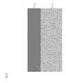
- FIGS. 1 through 4schematically illustrate a method for forming a capping layer on a hardmask layer, in accordance with an exemplary embodiment.
- a capping layeris formed over the hardmask layer to increase the overall performance of the hardmask layer with respect to etch resistance.
- Methodology in accordance with embodiments of the present disclosureincludes forming a hardmask layer over a substrate, and forming a capping layer on the hardmask layer, the capping layer including a stack of at least two nanolayers.
- the capping layermay include nanolayers of SiC, c-BN, or t-BN, or alternating nanolayers of SiC and SiCN, BN and TiN, or SiC and BN.
- a method of forming a capping layer over a hardmask layerbegins with a base layer 101 .
- the base layer 101may be any type of layer that may subsequently have a hardmask layer deposited on it or over it, such as an interlayer dielectric (ILD) or substrate in manufacturing a semiconductor device.
- ILDinterlayer dielectric
- a hardmask layer 201may be formed over the base layer 101 , as illustrated in FIG. 2 .
- the hardmask layer 201may be formed directly on the base layer 101 , or may be formed on one or more additional layers between the hardmask layer 201 and the base layer 101 , depending on the specifics of the process.
- the hardmask layer 201may be formed of TiN.
- An additional hardmask layer of tetraethyl orthosilicate (TEOS)(not shown for illustrative convenience) may be included beneath the hardmask layer 201 .
- TEOStetraethyl orthosilicate
- a capping layer 301may be formed on the hardmask layer 201 .
- the capping layer 301may be formed to a thickness of 10 to 30 nm and may be formed via deposition.
- the combination of the capping layer 301 and the hardmask layer 201may be formed to a thickness of less than or equal to 40 nm, such as 30 to 40 nm, as thicker hardmask and capping layers would undesirably increase the aspect ratio during later etching.
- the capping layer 301may be formed of at least two nanolayers 301 a and 301 b.
- the nanolayers 301 a and 301 bmay be repeating nanolayers of only SiC, c-BN, t-BN, or a combination thereof.
- a capping layer of SiCmay act as an etch stop layer over the TiN hardmask.
- the nanolayers 301 a and 301 bmay include alternating nanolayers of SiC and SiCN, BN and TiN, or SiC and BN.
- SiCis harder than TiN, and, therefore, is a desirable capping material for the TiN. Further, the higher the carbon content, the better the capping layer acts as an NBlok layer.
- the SiCshould be nanolayer 301 b , separated from the TiN hardmask layer, as SiC tends to delaminate from TiN.
- the nanolayer 301 amay be SiCN and the nanolayer 301 b may be SiC, and the nanolayers 301 a and 301 b may repeat to form a capping layer 301 .
- Each one of the nanolayers 301 a and 301 bmay be formed to a thickness of 0.5 to 10 nm, and the capping layer 301 may be formed to have 2 to 100 interfaces of the nanolayers 301 a and 301 b.
- Embodiments of the present disclosureachieve several technical effects, including improved etch resistance and increased the overall performance of a hardmask layer, thereby allowing the hardmask layer to be used in trench first metal hardmask schemes and double pattern VIA schemes.
- Embodiments of the present disclosureenjoy utility in various industrial applications as, for example, microprocessors, smart phones, mobile phones, cellular handsets, set-top boxes, DVD recorders and players, automotive navigation, printers and peripherals, networking and telecom equipment, gaming systems, and digital cameras. The present disclosure therefore enjoys industrial applicability in any of various types of highly integrated semiconductor devices.
Landscapes
- Chemical & Material Sciences (AREA)
- Engineering & Computer Science (AREA)
- Microelectronics & Electronic Packaging (AREA)
- Power Engineering (AREA)
- Condensed Matter Physics & Semiconductors (AREA)
- General Physics & Mathematics (AREA)
- Manufacturing & Machinery (AREA)
- Computer Hardware Design (AREA)
- Physics & Mathematics (AREA)
- Inorganic Chemistry (AREA)
- Chemical Kinetics & Catalysis (AREA)
- Materials Engineering (AREA)
- Mechanical Engineering (AREA)
- Metallurgy (AREA)
- Organic Chemistry (AREA)
- Ceramic Engineering (AREA)
- Internal Circuitry In Semiconductor Integrated Circuit Devices (AREA)
Abstract
Description
- The present disclosure relates to hardmask layers. The present disclosure is particularly applicable to hardmask layers with capping layers for increased etch resistance.
- Hardmasks are employed as etch masks for a variety of semiconductor manufacturing processes. Titanium nitride (TiN) hardmasks have been used, for example, for forming self-aligned vertical interconnect accesses (VIAs) (the simultaneous formation of a first layer metal and upper layer metal pattern and level (V0 and others) VIAs). However, TiN hardmask layers have poor etch resistance. The poor etch resistance prevents the hardmask layers from being used in processes related to, for example, trench first metal hardmask schemes, hardmask open schemes, and VIA double patterning schemes. Current conventional hardmask layers are also plagued by poor self-aligned VIA (SAV) performance as part of a dielectric etch. A marginal increase in the etch resistance of the hardmask layer will allow for critical functions like merged VIAs to be used with respect to new technology nodes. Merged VIAs will allow designers to fit more VIAs into a fixed space with no upgrade in lithography tool sets.
- A need therefore exists for methodology enabling formation of hardmask layers with increased etch resistance and hardmask layer performance, and the resulting device.
- An aspect of the present disclosure is an efficient method for forming a capping layer of nanolayers on a hardmask layer.
- Another aspect of the present disclosure is a hardmask layer having a capping layer of nanolayers thereon.
- Additional aspects and other features of the present disclosure will be set forth in the description which follows and in part will be apparent to those having ordinary skill in the art upon examination of the following or may be learned from the practice of the present disclosure. The advantages of the present disclosure may be realized and obtained as particularly pointed out in the appended claims.
- According to the present disclosure, some technical effects may be achieved in part by a method including: forming a hardmask layer over a substrate, and forming a capping layer on the hardmask layer, the capping layer including a stack of at least two nanolayers.
- Aspects of the present disclosure include forming the capping layer and the hardmask layer to a total thickness of less than or equal to 40 nanometers (nm). An additional aspect includes forming the capping layer and the hardmask layer to a total thickness of 30 to 40 nm. Another aspect includes forming the capping layer to a thickness of 10 to 30 nm. Another aspect includes the capping layer being formed of nanolayers of silicon carbide (SiC), cubic boron nitride (c-BN), or turbostatic boron nitride (t-BN), or alternating nanolayers of SiC and silicon carbon nitride (SiCN), BN and TiN, or SiC and BN.
- Another aspect of the present disclosure is a device including: a substrate, a hardmask layer over the substrate, and a capping layer on the hardmask layer, the capping layer including a stack of at least two nanolayers.
- Aspects include a thickness of the capping layer and the hardmask layer being less than 40 nm. Another aspect includes a thickness of the capping layer and the hardmask layer being 30 to 40 nm. A further aspect includes a thickness of the capping layer being 10 to 30 nm. Yet another aspect includes the capping layer including nanolayers of SiC, c-BN, or t-BN, or alternating nanolayers of SiC and SiCN, BN and TiN, or SiC and BN.
- Another aspect of the present disclosure includes: forming a TiN hardmask layer over a substrate, and forming a capping layer of at least two nanolayers on the TiN hardmask layer to a thickness of 10 to 30 nm, wherein a total thickness of the TiN hardmask layer and the capping layer ranges from 30 to 40 nm.
- Another aspect includes the capping layer formed of nanolayers of SiC or t-BN, or alternating nanolayers of SiC and SiCN, BN and TiN, or SiC and BN.
- Additional aspects and technical effects of the present disclosure will become readily apparent to those skilled in the art from the following detailed description wherein embodiments of the present disclosure are described simply by way of illustration of the best mode contemplated to carry out the present disclosure. As will be realized, the present disclosure is capable of other and different embodiments, and its several details are capable of modifications in various obvious respects, all without departing from the present disclosure. Accordingly, the drawings and description are to be regarded as illustrative in nature, and not as restrictive.
- The present disclosure is illustrated by way of example, and not by way of limitation, in the figures of the accompanying drawings and in which like reference numerals refer to similar elements and in which:
FIGS. 1 through 4 schematically illustrate a method for forming a capping layer on a hardmask layer, in accordance with an exemplary embodiment.- In the following description, for the purposes of explanation, numerous specific details are set forth in order to provide a thorough understanding of exemplary embodiments. It should be apparent, however, that exemplary embodiments may be practiced without these specific details or with an equivalent arrangement. In other instances, well-known structures and devices are shown in block diagram form in order to avoid unnecessarily obscuring exemplary embodiments. In addition, unless otherwise indicated, all numbers expressing quantities, ratios, and numerical properties of ingredients, reaction conditions, and so forth used in the specification and claims are to be understood as being modified in all instances by the term “about.”
- The present disclosure addresses and solves the current problem of poor etch resistance attendant upon etching through conventional hardmask layers. In accordance with embodiments of the present disclosure, a capping layer is formed over the hardmask layer to increase the overall performance of the hardmask layer with respect to etch resistance.
- Methodology in accordance with embodiments of the present disclosure includes forming a hardmask layer over a substrate, and forming a capping layer on the hardmask layer, the capping layer including a stack of at least two nanolayers. The capping layer may include nanolayers of SiC, c-BN, or t-BN, or alternating nanolayers of SiC and SiCN, BN and TiN, or SiC and BN.
- Adverting to
FIG. 1 , a method of forming a capping layer over a hardmask layer, in accordance with an exemplary embodiment, begins with abase layer 101. Thebase layer 101 may be any type of layer that may subsequently have a hardmask layer deposited on it or over it, such as an interlayer dielectric (ILD) or substrate in manufacturing a semiconductor device. - Next, a
hardmask layer 201 may be formed over thebase layer 101, as illustrated inFIG. 2 . Thehardmask layer 201 may be formed directly on thebase layer 101, or may be formed on one or more additional layers between thehardmask layer 201 and thebase layer 101, depending on the specifics of the process. Thehardmask layer 201 may be formed of TiN. An additional hardmask layer of tetraethyl orthosilicate (TEOS) (not shown for illustrative convenience) may be included beneath thehardmask layer 201. - Adverting to
FIG. 3 , acapping layer 301 may be formed on thehardmask layer 201. Thecapping layer 301 may be formed to a thickness of 10 to 30 nm and may be formed via deposition. The combination of thecapping layer 301 and thehardmask layer 201 may be formed to a thickness of less than or equal to 40 nm, such as 30 to 40 nm, as thicker hardmask and capping layers would undesirably increase the aspect ratio during later etching. - Further, as illustrated in
FIG. 4 , thecapping layer 301 may be formed of at least twonanolayers nanolayers nanolayers nanolayer 301b, separated from the TiN hardmask layer, as SiC tends to delaminate from TiN. For example, thenanolayer 301amay be SiCN and thenanolayer 301bmay be SiC, and thenanolayers capping layer 301. Each one of thenanolayers capping layer 301 may be formed to have 2 to 100 interfaces of thenanolayers nanolayers capping layer 301 remains constant, harder capping layers may be formed without increasing the residual stress. Rather, the residual stress is mitigated by the presence of the interfaces, which are believed to act as buffers and reduce the overall residual stress of thecapping layer 301 leading to acapping layer 301 with a lower residual stress than anysingle nanolayer capping layer 301. - The embodiments of the present disclosure achieve several technical effects, including improved etch resistance and increased the overall performance of a hardmask layer, thereby allowing the hardmask layer to be used in trench first metal hardmask schemes and double pattern VIA schemes. Embodiments of the present disclosure enjoy utility in various industrial applications as, for example, microprocessors, smart phones, mobile phones, cellular handsets, set-top boxes, DVD recorders and players, automotive navigation, printers and peripherals, networking and telecom equipment, gaming systems, and digital cameras. The present disclosure therefore enjoys industrial applicability in any of various types of highly integrated semiconductor devices.
- In the preceding description, the present disclosure is described with reference to specifically exemplary embodiments thereof. It will, however, be evident that various modifications and changes may be made thereto without departing from the broader spirit and scope of the present disclosure, as set forth in the claims. The specification and drawings are, accordingly, to be regarded as illustrative and not as restrictive. It is understood that the present disclosure is capable of using various other combinations and embodiments and is capable of any changes or modifications within the scope of the inventive concept as expressed herein.
Claims (20)
Priority Applications (2)
| Application Number | Priority Date | Filing Date | Title |
|---|---|---|---|
| US13/590,556US9028918B2 (en) | 2012-08-21 | 2012-08-21 | Forming a hardmask capping layer |
| US14/669,213US20150200093A1 (en) | 2012-08-21 | 2015-03-26 | Hardmask capping layer |
Applications Claiming Priority (1)
| Application Number | Priority Date | Filing Date | Title |
|---|---|---|---|
| US13/590,556US9028918B2 (en) | 2012-08-21 | 2012-08-21 | Forming a hardmask capping layer |
Related Child Applications (1)
| Application Number | Title | Priority Date | Filing Date |
|---|---|---|---|
| US14/669,213DivisionUS20150200093A1 (en) | 2012-08-21 | 2015-03-26 | Hardmask capping layer |
Publications (2)
| Publication Number | Publication Date |
|---|---|
| US20140057099A1true US20140057099A1 (en) | 2014-02-27 |
| US9028918B2 US9028918B2 (en) | 2015-05-12 |
Family
ID=50148230
Family Applications (2)
| Application Number | Title | Priority Date | Filing Date |
|---|---|---|---|
| US13/590,556Active2033-02-21US9028918B2 (en) | 2012-08-21 | 2012-08-21 | Forming a hardmask capping layer |
| US14/669,213AbandonedUS20150200093A1 (en) | 2012-08-21 | 2015-03-26 | Hardmask capping layer |
Family Applications After (1)
| Application Number | Title | Priority Date | Filing Date |
|---|---|---|---|
| US14/669,213AbandonedUS20150200093A1 (en) | 2012-08-21 | 2015-03-26 | Hardmask capping layer |
Country Status (1)
| Country | Link |
|---|---|
| US (2) | US9028918B2 (en) |
Cited By (2)
| Publication number | Priority date | Publication date | Assignee | Title |
|---|---|---|---|---|
| US10347488B2 (en) | 2015-09-19 | 2019-07-09 | Applied Materials, Inc. | Titanium compound based hard mask films |
| US11326247B2 (en)* | 2019-01-30 | 2022-05-10 | Industry-Academic Cooperation Foundation, Yonsei University | Transparent nanolayered structure having improved wear-resistant and flexibility |
Citations (9)
| Publication number | Priority date | Publication date | Assignee | Title |
|---|---|---|---|---|
| US20010012689A1 (en)* | 1998-12-03 | 2001-08-09 | Uzodinma Okoroanyanwu | Interconnect structure with silicon containing alicyclic polymers and low-k dieletric materials and method of making same with single and dual damascene techniques |
| US20060157684A1 (en)* | 2004-12-15 | 2006-07-20 | The Regents Of The University Of California | Thin film multilayer with nanolayers addressable from the macroscale |
| US20060269847A1 (en)* | 2005-05-25 | 2006-11-30 | International Business Machines Corporaton | Binding of hard pellicle structure to mask blank and method |
| WO2007116362A1 (en)* | 2006-04-07 | 2007-10-18 | Nxp B.V. | Method of manufacturing a semiconductor device |
| US20080299494A1 (en)* | 2007-06-01 | 2008-12-04 | Bencher Christopher D | Double patterning with a double layer cap on carbonaceous hardmask |
| US20090103069A1 (en)* | 2007-10-23 | 2009-04-23 | Interuniversitair Microelektronica Centrum Vzw (Imec) | Detection of contamination in euv systems |
| US20100093172A1 (en)* | 2008-10-09 | 2010-04-15 | Kim Hyoung-Hee | Method of forming fine patterns of a semiconductor device |
| US20110275218A1 (en)* | 2009-09-24 | 2011-11-10 | Taiwan Semiconductor Manufacturing Company, Ltd. | Double patterning strategy for contact hole and trench in photolithography |
| US8211510B1 (en)* | 2007-08-31 | 2012-07-03 | Novellus Systems, Inc. | Cascaded cure approach to fabricate highly tensile silicon nitride films |
- 2012
- 2012-08-21USUS13/590,556patent/US9028918B2/enactiveActive
- 2015
- 2015-03-26USUS14/669,213patent/US20150200093A1/ennot_activeAbandoned
Patent Citations (9)
| Publication number | Priority date | Publication date | Assignee | Title |
|---|---|---|---|---|
| US20010012689A1 (en)* | 1998-12-03 | 2001-08-09 | Uzodinma Okoroanyanwu | Interconnect structure with silicon containing alicyclic polymers and low-k dieletric materials and method of making same with single and dual damascene techniques |
| US20060157684A1 (en)* | 2004-12-15 | 2006-07-20 | The Regents Of The University Of California | Thin film multilayer with nanolayers addressable from the macroscale |
| US20060269847A1 (en)* | 2005-05-25 | 2006-11-30 | International Business Machines Corporaton | Binding of hard pellicle structure to mask blank and method |
| WO2007116362A1 (en)* | 2006-04-07 | 2007-10-18 | Nxp B.V. | Method of manufacturing a semiconductor device |
| US20080299494A1 (en)* | 2007-06-01 | 2008-12-04 | Bencher Christopher D | Double patterning with a double layer cap on carbonaceous hardmask |
| US8211510B1 (en)* | 2007-08-31 | 2012-07-03 | Novellus Systems, Inc. | Cascaded cure approach to fabricate highly tensile silicon nitride films |
| US20090103069A1 (en)* | 2007-10-23 | 2009-04-23 | Interuniversitair Microelektronica Centrum Vzw (Imec) | Detection of contamination in euv systems |
| US20100093172A1 (en)* | 2008-10-09 | 2010-04-15 | Kim Hyoung-Hee | Method of forming fine patterns of a semiconductor device |
| US20110275218A1 (en)* | 2009-09-24 | 2011-11-10 | Taiwan Semiconductor Manufacturing Company, Ltd. | Double patterning strategy for contact hole and trench in photolithography |
Non-Patent Citations (4)
| Title |
|---|
| Kim, Tae Geun, et al., "Characterization of Ru layer for capping/buffer application in EUVL mask". Microelectronic Engineering 83 (2006) 688-691.* |
| Lee, Jae-Young, et al., "Coating BaTiO3 Nanolayers on Spherical Ni Powders for Multilayers Ceramic Capacitors". Advanced Materials 2003, 15, No. 19, October 2, pp.1655-1658.* |
| Lee, Sang-Ho, et al., "Particle Adhesion and Removal on EUV Mask Layers During Wet Cleaning". Japanese Journal of Applied Physics, Vol.44, No.7B, 2005, pp.5479-5483.* |
| Tsarfati, Tim, et al., "Growth and sacrificial oxidation of transition metal nanolayers". Surface Science 603 (2009) 1041-1045.* |
Cited By (2)
| Publication number | Priority date | Publication date | Assignee | Title |
|---|---|---|---|---|
| US10347488B2 (en) | 2015-09-19 | 2019-07-09 | Applied Materials, Inc. | Titanium compound based hard mask films |
| US11326247B2 (en)* | 2019-01-30 | 2022-05-10 | Industry-Academic Cooperation Foundation, Yonsei University | Transparent nanolayered structure having improved wear-resistant and flexibility |
Also Published As
| Publication number | Publication date |
|---|---|
| US9028918B2 (en) | 2015-05-12 |
| US20150200093A1 (en) | 2015-07-16 |
Similar Documents
| Publication | Publication Date | Title |
|---|---|---|
| US8962474B2 (en) | Method for forming an air gap around a through-silicon via | |
| US8518775B2 (en) | Integration of eNVM, RMG, and HKMG modules | |
| US9842801B2 (en) | Self-aligned via and air gap | |
| US11011421B2 (en) | Semiconductor device having voids and method of forming same | |
| US10937689B2 (en) | Self-aligned hard masks with converted liners | |
| US20170141039A1 (en) | Method of forming stacked trench contacts and structures formed thereby | |
| US20150162416A1 (en) | Spacers with Rectangular Profile and Methods of Forming the Same | |
| TWI574373B (en) | Integrated circuit device and forming method thereof | |
| US20140151888A1 (en) | Air-Gap Formation in Interconnect Structures | |
| US20140252624A1 (en) | Semiconductor Devices and Methods of Forming Same | |
| US8927386B2 (en) | Method for manufacturing deep-trench super PN junctions | |
| US9318437B1 (en) | Moisture scavenging layer for thinner barrier application in beol integration | |
| US20140273437A1 (en) | Subtractive plasma etching of a blanket layer of metal or metal alloy | |
| CN105336680A (en) | Semiconductor device, manufacturing method thereof and electronic device | |
| US20150236091A1 (en) | Porous insulation film, and a semiconductor device including such porous insulation film | |
| US20150348834A1 (en) | Hard Mask Removal Scheme | |
| US9028918B2 (en) | Forming a hardmask capping layer | |
| US10020202B2 (en) | Fabrication of multi threshold-voltage devices | |
| US8736014B2 (en) | High mechanical strength additives for porous ultra low-k material | |
| US12113113B2 (en) | Semiconductor device with a core-shell feature and method for forming the same | |
| US9373680B1 (en) | Integrated circuits with capacitors and methods of producing the same | |
| US8900665B2 (en) | Method of forming hardmask layer with alternating nanolayers | |
| KR102379950B1 (en) | Semiconductor device and method the same | |
| US9343406B2 (en) | Device having self-repair Cu barrier for solving barrier degradation due to Ru CMP | |
| CN105097500A (en) | Semiconductor device and method for manufacturing the semiconductor device, and electronic apparatus |
Legal Events
| Date | Code | Title | Description |
|---|---|---|---|
| AS | Assignment | Owner name:GLOBALFOUNDRIES INC., CAYMAN ISLANDS Free format text:ASSIGNMENT OF ASSIGNORS INTEREST;ASSIGNOR:KOSHY, ROBIN ABRAHAM;REEL/FRAME:028820/0587 Effective date:20120815 | |
| FEPP | Fee payment procedure | Free format text:PAYOR NUMBER ASSIGNED (ORIGINAL EVENT CODE: ASPN); ENTITY STATUS OF PATENT OWNER: LARGE ENTITY | |
| STCF | Information on status: patent grant | Free format text:PATENTED CASE | |
| MAFP | Maintenance fee payment | Free format text:PAYMENT OF MAINTENANCE FEE, 4TH YEAR, LARGE ENTITY (ORIGINAL EVENT CODE: M1551); ENTITY STATUS OF PATENT OWNER: LARGE ENTITY Year of fee payment:4 | |
| AS | Assignment | Owner name:WILMINGTON TRUST, NATIONAL ASSOCIATION, DELAWARE Free format text:SECURITY AGREEMENT;ASSIGNOR:GLOBALFOUNDRIES INC.;REEL/FRAME:049490/0001 Effective date:20181127 | |
| AS | Assignment | Owner name:GLOBALFOUNDRIES U.S. INC., CALIFORNIA Free format text:ASSIGNMENT OF ASSIGNORS INTEREST;ASSIGNOR:GLOBALFOUNDRIES INC.;REEL/FRAME:054633/0001 Effective date:20201022 | |
| AS | Assignment | Owner name:GLOBALFOUNDRIES INC., CAYMAN ISLANDS Free format text:RELEASE BY SECURED PARTY;ASSIGNOR:WILMINGTON TRUST, NATIONAL ASSOCIATION;REEL/FRAME:054636/0001 Effective date:20201117 | |
| AS | Assignment | Owner name:GLOBALFOUNDRIES U.S. INC., NEW YORK Free format text:RELEASE BY SECURED PARTY;ASSIGNOR:WILMINGTON TRUST, NATIONAL ASSOCIATION;REEL/FRAME:056987/0001 Effective date:20201117 | |
| MAFP | Maintenance fee payment | Free format text:PAYMENT OF MAINTENANCE FEE, 8TH YEAR, LARGE ENTITY (ORIGINAL EVENT CODE: M1552); ENTITY STATUS OF PATENT OWNER: LARGE ENTITY Year of fee payment:8 |