US20140030533A1 - Innovative top-coat approach for advanced device on-wafer particle performance - Google Patents
Innovative top-coat approach for advanced device on-wafer particle performanceDownload PDFInfo
- Publication number
- US20140030533A1 US20140030533A1US13/759,525US201313759525AUS2014030533A1US 20140030533 A1US20140030533 A1US 20140030533A1US 201313759525 AUS201313759525 AUS 201313759525AUS 2014030533 A1US2014030533 A1US 2014030533A1
- Authority
- US
- United States
- Prior art keywords
- article
- sol
- gel coating
- plasma
- gel
- Prior art date
- Legal status (The legal status is an assumption and is not a legal conclusion. Google has not performed a legal analysis and makes no representation as to the accuracy of the status listed.)
- Granted
Links
- 239000002245particleSubstances0.000titledescription22
- 238000000576coating methodMethods0.000claimsabstractdescription115
- 239000011248coating agentSubstances0.000claimsabstractdescription109
- RUDFQVOCFDJEEF-UHFFFAOYSA-Nyttrium(III) oxideInorganic materials[O-2].[O-2].[O-2].[Y+3].[Y+3]RUDFQVOCFDJEEF-UHFFFAOYSA-N0.000claimsabstractdescription63
- 238000000034methodMethods0.000claimsabstractdescription44
- 238000004519manufacturing processMethods0.000claimsabstractdescription14
- 238000010438heat treatmentMethods0.000claimsabstractdescription10
- 239000004065semiconductorSubstances0.000claimsabstractdescription10
- 239000000758substrateSubstances0.000claimsdescription14
- 238000011065in-situ storageMethods0.000claimsdescription8
- 235000012431wafersNutrition0.000claimsdescription7
- 238000005507sprayingMethods0.000claimsdescription6
- 239000002184metalSubstances0.000claimsdescription5
- PNEYBMLMFCGWSK-UHFFFAOYSA-Naluminium oxideInorganic materials[O-2].[O-2].[O-2].[Al+3].[Al+3]PNEYBMLMFCGWSK-UHFFFAOYSA-N0.000claimsdescription4
- 229910052593corundumInorganic materials0.000claimsdescription4
- 229910001845yogo sapphireInorganic materials0.000claimsdescription4
- 210000002381plasmaAnatomy0.000description81
- 238000001723curingMethods0.000description32
- 238000010943off-gassingMethods0.000description9
- 239000011148porous materialSubstances0.000description7
- 238000007789sealingMethods0.000description6
- 238000005033Fourier transform infrared spectroscopyMethods0.000description4
- 239000000919ceramicSubstances0.000description4
- 238000007598dipping methodMethods0.000description4
- 230000003628erosive effectEffects0.000description4
- 239000000463materialSubstances0.000description4
- 229910052760oxygenInorganic materials0.000description4
- 239000002243precursorSubstances0.000description4
- 238000004458analytical methodMethods0.000description3
- QVGXLLKOCUKJST-UHFFFAOYSA-Natomic oxygenChemical compound[O]QVGXLLKOCUKJST-UHFFFAOYSA-N0.000description3
- 238000004140cleaningMethods0.000description3
- 238000011109contaminationMethods0.000description3
- 238000002149energy-dispersive X-ray emission spectroscopyMethods0.000description3
- 239000001307heliumSubstances0.000description3
- 229910052734heliumInorganic materials0.000description3
- SWQJXJOGLNCZEY-UHFFFAOYSA-Nhelium atomChemical compound[He]SWQJXJOGLNCZEY-UHFFFAOYSA-N0.000description3
- 230000003993interactionEffects0.000description3
- 239000001301oxygenSubstances0.000description3
- 238000010422paintingMethods0.000description3
- 238000003980solgel methodMethods0.000description3
- 238000001029thermal curingMethods0.000description3
- OKTJSMMVPCPJKN-UHFFFAOYSA-NCarbonChemical compound[C]OKTJSMMVPCPJKN-UHFFFAOYSA-N0.000description2
- 230000015572biosynthetic processEffects0.000description2
- 229910052799carbonInorganic materials0.000description2
- 230000007547defectEffects0.000description2
- 238000011049fillingMethods0.000description2
- 238000010884ion-beam techniqueMethods0.000description2
- 230000005540biological transmissionEffects0.000description1
- 238000001311chemical methods and processMethods0.000description1
- 239000000470constituentSubstances0.000description1
- 239000000356contaminantSubstances0.000description1
- 238000005260corrosionMethods0.000description1
- 230000007797corrosionEffects0.000description1
- 230000000593degrading effectEffects0.000description1
- 238000010586diagramMethods0.000description1
- 238000005530etchingMethods0.000description1
- 235000011194food seasoning agentNutrition0.000description1
- 239000007791liquid phaseSubstances0.000description1
- 238000012423maintenanceMethods0.000description1
- 229910044991metal oxideInorganic materials0.000description1
- 150000004706metal oxidesChemical class0.000description1
- NJPPVKZQTLUDBO-UHFFFAOYSA-NnovaluronChemical compoundC1=C(Cl)C(OC(F)(F)C(OC(F)(F)F)F)=CC=C1NC(=O)NC(=O)C1=C(F)C=CC=C1FNJPPVKZQTLUDBO-UHFFFAOYSA-N0.000description1
- 239000003973paintSubstances0.000description1
- 230000035515penetrationEffects0.000description1
- 229920000642polymerPolymers0.000description1
- 238000011417postcuringMethods0.000description1
- 239000007790solid phaseSubstances0.000description1
- 239000007921spraySubstances0.000description1
- 239000000126substanceSubstances0.000description1
- 230000003746surface roughnessEffects0.000description1
- 229920001187thermosetting polymerPolymers0.000description1
Images


Classifications
- B—PERFORMING OPERATIONS; TRANSPORTING
- B05—SPRAYING OR ATOMISING IN GENERAL; APPLYING FLUENT MATERIALS TO SURFACES, IN GENERAL
- B05D—PROCESSES FOR APPLYING FLUENT MATERIALS TO SURFACES, IN GENERAL
- B05D3/00—Pretreatment of surfaces to which liquids or other fluent materials are to be applied; After-treatment of applied coatings, e.g. intermediate treating of an applied coating preparatory to subsequent applications of liquids or other fluent materials
- B05D3/14—Pretreatment of surfaces to which liquids or other fluent materials are to be applied; After-treatment of applied coatings, e.g. intermediate treating of an applied coating preparatory to subsequent applications of liquids or other fluent materials by electrical means
- B05D3/141—Plasma treatment
- B05D3/145—After-treatment
- B05D3/147—Curing
- H—ELECTRICITY
- H01—ELECTRIC ELEMENTS
- H01J—ELECTRIC DISCHARGE TUBES OR DISCHARGE LAMPS
- H01J37/00—Discharge tubes with provision for introducing objects or material to be exposed to the discharge, e.g. for the purpose of examination or processing thereof
- H01J37/32—Gas-filled discharge tubes
- H01J37/32431—Constructional details of the reactor
- H01J37/32458—Vessel
- H01J37/32477—Vessel characterised by the means for protecting vessels or internal parts, e.g. coatings
- C—CHEMISTRY; METALLURGY
- C23—COATING METALLIC MATERIAL; COATING MATERIAL WITH METALLIC MATERIAL; CHEMICAL SURFACE TREATMENT; DIFFUSION TREATMENT OF METALLIC MATERIAL; COATING BY VACUUM EVAPORATION, BY SPUTTERING, BY ION IMPLANTATION OR BY CHEMICAL VAPOUR DEPOSITION, IN GENERAL; INHIBITING CORROSION OF METALLIC MATERIAL OR INCRUSTATION IN GENERAL
- C23C—COATING METALLIC MATERIAL; COATING MATERIAL WITH METALLIC MATERIAL; SURFACE TREATMENT OF METALLIC MATERIAL BY DIFFUSION INTO THE SURFACE, BY CHEMICAL CONVERSION OR SUBSTITUTION; COATING BY VACUUM EVAPORATION, BY SPUTTERING, BY ION IMPLANTATION OR BY CHEMICAL VAPOUR DEPOSITION, IN GENERAL
- C23C18/00—Chemical coating by decomposition of either liquid compounds or solutions of the coating forming compounds, without leaving reaction products of surface material in the coating; Contact plating
- C23C18/02—Chemical coating by decomposition of either liquid compounds or solutions of the coating forming compounds, without leaving reaction products of surface material in the coating; Contact plating by thermal decomposition
- C23C18/12—Chemical coating by decomposition of either liquid compounds or solutions of the coating forming compounds, without leaving reaction products of surface material in the coating; Contact plating by thermal decomposition characterised by the deposition of inorganic material other than metallic material
- C23C18/1204—Chemical coating by decomposition of either liquid compounds or solutions of the coating forming compounds, without leaving reaction products of surface material in the coating; Contact plating by thermal decomposition characterised by the deposition of inorganic material other than metallic material inorganic material, e.g. non-oxide and non-metallic such as sulfides, nitrides based compounds
- C23C18/1208—Oxides, e.g. ceramics
- C23C18/1216—Metal oxides
- C—CHEMISTRY; METALLURGY
- C23—COATING METALLIC MATERIAL; COATING MATERIAL WITH METALLIC MATERIAL; CHEMICAL SURFACE TREATMENT; DIFFUSION TREATMENT OF METALLIC MATERIAL; COATING BY VACUUM EVAPORATION, BY SPUTTERING, BY ION IMPLANTATION OR BY CHEMICAL VAPOUR DEPOSITION, IN GENERAL; INHIBITING CORROSION OF METALLIC MATERIAL OR INCRUSTATION IN GENERAL
- C23C—COATING METALLIC MATERIAL; COATING MATERIAL WITH METALLIC MATERIAL; SURFACE TREATMENT OF METALLIC MATERIAL BY DIFFUSION INTO THE SURFACE, BY CHEMICAL CONVERSION OR SUBSTITUTION; COATING BY VACUUM EVAPORATION, BY SPUTTERING, BY ION IMPLANTATION OR BY CHEMICAL VAPOUR DEPOSITION, IN GENERAL
- C23C18/00—Chemical coating by decomposition of either liquid compounds or solutions of the coating forming compounds, without leaving reaction products of surface material in the coating; Contact plating
- C23C18/02—Chemical coating by decomposition of either liquid compounds or solutions of the coating forming compounds, without leaving reaction products of surface material in the coating; Contact plating by thermal decomposition
- C23C18/12—Chemical coating by decomposition of either liquid compounds or solutions of the coating forming compounds, without leaving reaction products of surface material in the coating; Contact plating by thermal decomposition characterised by the deposition of inorganic material other than metallic material
- C23C18/1229—Composition of the substrate
- C23C18/1245—Inorganic substrates other than metallic
- C—CHEMISTRY; METALLURGY
- C23—COATING METALLIC MATERIAL; COATING MATERIAL WITH METALLIC MATERIAL; CHEMICAL SURFACE TREATMENT; DIFFUSION TREATMENT OF METALLIC MATERIAL; COATING BY VACUUM EVAPORATION, BY SPUTTERING, BY ION IMPLANTATION OR BY CHEMICAL VAPOUR DEPOSITION, IN GENERAL; INHIBITING CORROSION OF METALLIC MATERIAL OR INCRUSTATION IN GENERAL
- C23C—COATING METALLIC MATERIAL; COATING MATERIAL WITH METALLIC MATERIAL; SURFACE TREATMENT OF METALLIC MATERIAL BY DIFFUSION INTO THE SURFACE, BY CHEMICAL CONVERSION OR SUBSTITUTION; COATING BY VACUUM EVAPORATION, BY SPUTTERING, BY ION IMPLANTATION OR BY CHEMICAL VAPOUR DEPOSITION, IN GENERAL
- C23C18/00—Chemical coating by decomposition of either liquid compounds or solutions of the coating forming compounds, without leaving reaction products of surface material in the coating; Contact plating
- C23C18/02—Chemical coating by decomposition of either liquid compounds or solutions of the coating forming compounds, without leaving reaction products of surface material in the coating; Contact plating by thermal decomposition
- C23C18/12—Chemical coating by decomposition of either liquid compounds or solutions of the coating forming compounds, without leaving reaction products of surface material in the coating; Contact plating by thermal decomposition characterised by the deposition of inorganic material other than metallic material
- C23C18/125—Process of deposition of the inorganic material
- C23C18/1254—Sol or sol-gel processing
- C—CHEMISTRY; METALLURGY
- C23—COATING METALLIC MATERIAL; COATING MATERIAL WITH METALLIC MATERIAL; CHEMICAL SURFACE TREATMENT; DIFFUSION TREATMENT OF METALLIC MATERIAL; COATING BY VACUUM EVAPORATION, BY SPUTTERING, BY ION IMPLANTATION OR BY CHEMICAL VAPOUR DEPOSITION, IN GENERAL; INHIBITING CORROSION OF METALLIC MATERIAL OR INCRUSTATION IN GENERAL
- C23C—COATING METALLIC MATERIAL; COATING MATERIAL WITH METALLIC MATERIAL; SURFACE TREATMENT OF METALLIC MATERIAL BY DIFFUSION INTO THE SURFACE, BY CHEMICAL CONVERSION OR SUBSTITUTION; COATING BY VACUUM EVAPORATION, BY SPUTTERING, BY ION IMPLANTATION OR BY CHEMICAL VAPOUR DEPOSITION, IN GENERAL
- C23C18/00—Chemical coating by decomposition of either liquid compounds or solutions of the coating forming compounds, without leaving reaction products of surface material in the coating; Contact plating
- C23C18/02—Chemical coating by decomposition of either liquid compounds or solutions of the coating forming compounds, without leaving reaction products of surface material in the coating; Contact plating by thermal decomposition
- C23C18/12—Chemical coating by decomposition of either liquid compounds or solutions of the coating forming compounds, without leaving reaction products of surface material in the coating; Contact plating by thermal decomposition characterised by the deposition of inorganic material other than metallic material
- C23C18/125—Process of deposition of the inorganic material
- C23C18/1295—Process of deposition of the inorganic material with after-treatment of the deposited inorganic material
- H—ELECTRICITY
- H01—ELECTRIC ELEMENTS
- H01L—SEMICONDUCTOR DEVICES NOT COVERED BY CLASS H10
- H01L21/00—Processes or apparatus adapted for the manufacture or treatment of semiconductor or solid state devices or of parts thereof
- H01L21/67—Apparatus specially adapted for handling semiconductor or electric solid state devices during manufacture or treatment thereof; Apparatus specially adapted for handling wafers during manufacture or treatment of semiconductor or electric solid state devices or components ; Apparatus not specifically provided for elsewhere
Definitions
- Embodiments of the present inventionrelate, in general, to ceramic coated articles and to a process for applying a Y 2 O 3 sol-gel coating to a substrate.
- devicesare fabricated by a number of manufacturing processes producing structures of an ever-decreasing size.
- Some manufacturing processessuch as plasma etch and plasma clean processes expose a substrate to a high-speed stream of plasma to etch or clean the substrate.
- the plasmamay be highly corrosive, and may corrode processing chambers and other surfaces that are exposed to the plasma. This corrosion may generate particles, which frequently contaminate the substrate that is being processed, contributing to device defects.
- FIG. 1illustrates chamber on-wafer particle performance showing a number of particle adders over time (RFhrs) for a plasma screen before and after coating application over it according to one embodiment.
- FIG. 2illustrates a top scanning electron microscope (SEM) view of sol-gel Y2O3 coatings of various thicknesses over a plasma sprayed Y2O3 coating according to one embodiment.
- SEMscanning electron microscope
- FIG. 3Aillustrates a cross-sectional transmission electron microscope (TEM) view of an article with a sol-gel Y2O3 coating over a plasma sprayed Y 2 O 3 coating according to one embodiment.
- TEMtransmission electron microscope
- FIG. 3Billustrates a top TEM view of an article with a sol-gel Y2O3 coating over a plasma sprayed Y2O3 coating according to one embodiment.
- FIG. 4illustrates a cross-sectional focused ion beam (FIB) view of an article with a sol-gel Y2O3 coating over a plasma sprayed Y 2 O 3 coating according to one embodiment.
- FIBfocused ion beam
- FIG. 5illustrates a Fourier transform infrared spectroscopy (FTIR) analysis of various curing methods for the sol-gel Y2O3 coating according embodiments.
- FTIRFourier transform infrared spectroscopy
- FIG. 6Aillustrates outgassing showing total mass loss over time for a plasma sprayed Y 2 O 3 coating.
- FIG. 6Billustrates outgassing showing total mass loss over time for a sol-gel Y 2 O 3 coating over a plasma sprayed Y2O3 coating according to one embodiment.
- FIG. 7illustrates a method according to one embodiment.
- Embodiments of the inventionare directed to a process for coating a substrate with a Y 2 O 3 sol-gel coating, and to an article created using such a coating process.
- a sol-gel coating of Y 2 O 3can be applied to an article (e.g., a semiconductor manufacturing article).
- a vacuumcan then be applied to the article with the sol-gel coating.
- the sol-gel coatingcan be cured on the article by heating the article with the sol-gel coating, and exposing the article with the sol-gel coating to plasma in a chamber (e.g., a semiconductor manufacturing chamber).
- Semiconductor manufacturing articlese.g., chamber components
- semiconductor manufacturing articlesthat can be treated using the sol-gel coating process described herein include, but are not limited to, a dielectric showerhead, a chamber liner and an electrostatic chuck.
- Other manufacturing articles that may be treated using the sol-gel processinclude a chamber lid and process kit.
- One embodimentincludes a thin sol-gel Y 2 O 3 (Yttria) top coat (e.g., about 20 nm to about 150 nm) over either an existing plasma sprayed Y 2 O 3 layer or an anodized layer (e.g., about 3 mil (0.003′′)).
- the sol-gel processis a wet-chemical technique that may be used for ceramic engineering.
- the sol-gel processmay be used for the fabrication of materials (e.g., metal oxides) starting from a colloidal solution (sol) that acts as the precursor for an integrated network (or gel) of either discrete particles or network polymers.
- the ‘sol’ (or solution)gradually evolves towards the formation of a gel-like diphasic system containing both a liquid phase and solid phase whose morphologies range from discrete particles to continuous polymer networks.
- Current showerheadscan be made of an anodized Al base bonded to a SiC faceplate. Such showerheads may be susceptible to the formation of AlF due to plasma interaction with the anodized Al base. A high erosion rate of the anodized Al base can lead to arcing and can reduce the mean time between cleaning (MTBC) of the showerhead, leading to increased maintenance times and reduced productivity of the semiconductor manufacturing chamber.
- MTBCmean time between cleaning
- Some liner kitscan be made of an Al substrate coated with 8-12 mil of plasma sprayed Y 2 O 3 on an inner side (or interior surfaces) of the liner kit and anodized Al on an outer side (or exterior surfaces) of the liner kit.
- the on-wafer particle requirementis stringent (e.g., less than 1.3 adders at greater than 45 nm size).
- Chamber tests using the plasma sprayed Y 2 O 3 coated liner kits under reducing chemistryhave shown on-wafer particle levels, with predominantly Y 2 O 3 based particles, that are higher than particle requirements (e.g., greater than 100 adders at greater than 45 nm particle size).
- the on-wafer particle requirementcan be met.
- lengthy chamber exposuremay not be feasible in a production set-up, and increases the cost of the chamber liner kit.
- Electrostatic chucksinclude an electrostatic puck having a chucking electrode that electrostatically holds (chucks) a supported substrate (e.g., a wafer).
- a chucking electrodethat electrostatically holds (chucks) a supported substrate (e.g., a wafer).
- Such electrostatic pucksmay be composed of ceramics such as Al 2 O 3 or MN, for example, and may be bonded to an anodized Al base. Plasma chemistry erodes these materials, which may produce on-wafer particles and metal contamination.
- a surface of the electrostatic puckmay have features such as mesas and grooves that are filled with helium during processing.
- an outer ring on the surface of the electrostatic puckmay act as a seal between the substrate and the electrostatic puck.
- Heliummay be pumped into the grooves on the ESC via helium holes in the electrostatic puck to cool the wafer as well as ESC during processing.
- the ESC surfaceis degraded due to plasma erosion and He leaks at the edges of the ESC (e.g., at the outer seal band).
- ICCin-situ chamber cleaning
- He leakreaches a threshold value ( ⁇ 1.5 sccm-standard cubic centimeter per minute) the chamber stops processing.
- the ESChas to be taken out and replaced with a new or repaired ESC. This involves chamber down-time and reduces productivity.
- a sol-gel coatingcan be applied over both the Y 2 O 3 plasma coated side as well as the anodized backside of liner kits.
- the sol-gel coatingcan also be applied over the anodized base of ESCs, over the electrostatic puck of ESCs and over showerheads.
- the sol-gel coatingcan fill in surface cracks and pores present on plasma coated Y 2 O 3 , and form a sealing layer, such that on-wafer particle performance is improved because particles are less likely to be dislodged from articles with this coating during use.
- FIG. 1illustrates chamber on-wafer particle performance before and after applying sol-gel Y 2 O 3 coating to a plasma screen that surrounds the wafer to equalize plasma flow around the wafer (alternatively known as a flow equalizer).
- Portion 101shows the number of particle adders over time (RF hours) for a plasma screen with a plasma sprayed Y 2 O 3 layer and without a sol-gel coating
- portion 102shows the number of particle adders over time (RF hours) for the same plasma screen after a sol-gel Y 2 O 3 coating has been applied.
- particle performanceis improved with the addition of the sol-gel coating.
- the number of 45 nm addershas been significantly improved with the addition of the sol-gel coating.
- the number of 45 nm addersranges from about 10 to about 70 in portion 101 , where the sol-gel coating has not been applied, and the number of 45 nm adders ranges from about 0 to about 21 in portion 102 , where the sol-gel coating has been applied.
- the thickness of the sol-gel coatingcan be optimized such that the sol-gel fills in cracks and pores of a plasma coated surface, and forms a sealing layer over the surface.
- a Y 2 O 3 sol-gel top coatcan be applied to the liner kit (e.g., via spraying, dipping, or painting).
- sprayingthe thickness can be controlled by controlling the number of spray passes.
- paintingthe thickness can be controlled by the number of paint passes.
- thicknesscan controlled by dipping time (i.e., higher dip time corresponds to thicker coating).
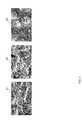
- FIG. 2illustrates a top SEM view of sol-gel Y 2 O 3 coatings of various thicknesses on an article having a plasma coated Y 2 O 3 layer prior to curing.
- Image 201shows a 30 nm sol-gel coating
- image 202shows a 60 nm sol-gel coating
- image 203shows a 110 nm sol-gel coating.
- EDSenergy-dispersive x-ray spectroscopy
- Carbon (C) %increases with an increase in coating thickness, which indicates higher sol-gel content. Carbon is a major constituent of the pre-cursor used in sol-gel and hence a higher C content indicates higher sol-gel content.
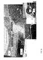
- FIG. 3Aillustrates a cross-sectional TEM view of an article 403 with a plasma coated Y 2 O 3 layer 402 with a 60 nm un-cured sol-gel coating 401 over the plasma coated Y 2 O 3 layer 402 .
- the sol-gel coating 401forms a sealing layer over the plasma coated Y 2 O 3 layer 402 on the article 403 .
- capillary forcewicks the sol-gel coating 401 into cracks on the plasma coated Y 2 O 3 layer.
- a loose Y 2 O 3 nodule 404is sealed by the sol-gel coating 401 .
- FIG. 3Billustrates a top TEM view of an article with a 60 nm un-cured sol-gel Y 2 O 3 coating.
- the sol-gel coatingcan be seen filling (or partially filling) in a crack 405 .
- EDS analysisshows the presence of Y and O elements deep in to the surface cracks on the plasma coated Y 2 O 3 layer, confirming the crack are filled with sol-gel Y 2 O 3 .
- the articleis placed in a vacuum prior to curing of the sol-gel coating.
- the vacuumcan improve penetration of the sol-gel coating into pores and cracks in the article or in the plasma coated Y 2 O 3 layer on the article.
- sol-gel Y 2 O 3 coatingscan be cured thermally (e.g., at about 400 degrees C.), articles having a plasma sprayed coating over bare Al substrate have a high coefficient of thermal expansion (CTE) mismatch between the plasma coated Y 2 O 3 layer and the Al substrate at elevated temperatures. Therefore, conventional thermal curing for these articles may not be feasible.
- sol-gel coated articlescan be cured using plasma assisted in-situ curing at lower temperatures. Curing of the sol-gel layer at low temperature can be achieved by plasma assisted in-chamber curing. This can be achieved in-situ in a plasma etch chamber prior to running the etching sequence by methods such as CH 4 /O 2 plasma assisted curing, O 2 plasma assisted curing, O 3 assisted curing, O 2 radical assisted curing.
- the sol-gel coatingcan be cured in a two-step process, where the article with the sol-gel coating is first thermally cured at about 110 degrees C. for about six hours, and is then cured in-chamber via plasma assisted curing.
- the thermal curing and the plasma assisted curingcan be performed sequentially, the thermal curing and the plasma assisted curing can alternatively occur in parallel (e.g., such that the sol-gel is exposed to a plasma assisted curing process at an elevated temperature).
- the duration of the exposure to plasma for curing, along with other parameters of the plasma assisted curingcan be optimized for the particular application and article.
- the articlemay be cured in the following plasma assisted conditions: (1) O 3 plasma—10 slm (standard liters per minute) O 3 flow, 130 degrees C.; (2) O 2 radical plasma—3500 sccm O 2 +350 sccm N 2 , pressure at 2T, source power at 5000 W, pedestal at 130 degrees C.
- O 3 plasma10 slm (standard liters per minute) O 3 flow, 130 degrees C.
- O 2 radical plasma3500 sccm O 2 +350 sccm N 2 , pressure at 2T, source power at 5000 W, pedestal at 130 degrees C.
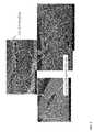
- FIG. 4illustrates a cross-sectional focused ion beam (FIB) view of an article with a plasma coated Y 2 O 3 layer and with a cured sol-gel Y 2 O 3 coating.
- FIBfocused ion beam
- the sol-gelpenetrates deeply into the cracks of the Y 2 O 3 layer and fills them.
- the thickness of the sol-gel coatingcan vary depending on the local surface roughness.
- FIG. 5illustrates a Fourier transform infrared spectroscopy (FTIR) analysis showing bonding states as a percentage of reflectance over wave numbers for various in-situ curing methods for a 110 nm Y 2 O 3 sol-gel coating.
- FTIRFourier transform infrared spectroscopy
- the O 2 plasma curing processmay be more effective than an O 2 radical curing process (O 2 radical edge) (which was the third most effective of the tested methods), which in turn may be more effective than an O 3 radical curing process (O 3 cured edge) (which was the least effective of the tested methods), as compared to the pre-cured sol-gel coating on spray coating edge.
- O 2 radical edgewhich was the third most effective of the tested methods
- O 3 radical curing processO 3 cured edge
- CH 3 /CH 2 stretching vibrationsare signs confirming a presence of significant pre-cursors.
- the goal of curingis to reduce or eliminate the pre-cursors. Therefore, curing that shows fewer CH 3 /CH 2 stretching vibration confirms more effective curing of the sol-gel coating.
- the thickness of the sol-gel coatingcan shrink by about 100 times.
- the thickness of the sol-gel coatingcan be optimized such that the sol-gel fills in the cracks and pores as well as forms a sealing layer once the sol-gel coating is cured.
- a post-cure thickness of about 110 nm sol-gel over the plasma sprayed Y 2 O 3 layeris desirable.
- sol-gel coatingDue to the sealing of the surface cracks and pores of underlying surfaces using the sol-gel technique, articles with the sol-gel coating can be cleaned with aggressive chemistries without chemically attacking the underneath substrate or degrading the coating adhesion, allowing for a wider and robust cleaning process window. Further, the erosion of all parts having anodized layers and plasma sprayed layers can be improved by the sol-gel coating, which fills in the cracks and pores, hence reducing plasma interaction.
- FIG. 6Aillustrates outgassing showing total mass loss over time for a plasma coated Y 2 O 3 layer baked for about 3 hours to about 24 hours
- FIG. 6Billustrates outgassing showing total mass loss over time for a plasma coated Y 2 O 3 layer with a sol-gel Y 2 O 3 coating.
- the outgassing resultsshow comparable outgassing rates between plasma sprayed Y 2 O 3 with and without the sol-gel sealing coating. In other words, the sol-gel coating does not significantly increase outgassing.
- FIG. 7illustrates a method 700 of coating an article with a sol-gel layer of Y 2 O 3 .
- the articlemay be an electrostatic chuck, a showerhead, a chamber liner kit, or other chamber component.
- the articlemay be an anodized metal, a ceramic (e.g., MN, AlO2, Y2O3, etc.), or other materials.
- the sol-gel of Y 2 O 3can be applied (e.g., via spraying, dipping, or painting) to an article (e.g., a liner kit, a showerhead, or an ESC).
- a vacuumcan be optionally applied to the article after the sol-gel coating is applied, such that the sol-gel coating will better penetrate into the cracks and pores in the article (especially if the article is plasma coated).
- the magnitude and duration of the vacuumcan be optimized for the particular article.
- the vacuumcan be applied in a range from about 10 mT to about 300 mT, and the vacuum can be applied for a time period in a range from about 1 hours to about 12 hours.
- the article with the sol-gel coating appliedcan be heated.
- the article with the sol-gel appliedcan be heated to about 100 degrees C. for about six hours.
- the temperature and durationcan be optimized for the particular article.
- the articlecan be heated to a temperature in a range from about 100 C to about 500 C, for a time period in a range from about 1 hour to about 12 hours.
- the article with the sol-gel coating appliedcan be exposed to plasma in-situ curing.
- the articlecan be installed in a plasma etch chamber to be exposed to the plasma.
- the sol-gel coated articlecan be installed into a chamber that it will be used in, and can be exposed to a CH4/O2 plasma (or other plasma) to cure the sol-gel coating.
- the sol-gel coated articlemay remain in the chamber, and may be used to process substrates (e.g., wafers).
- an ESC having a sol-gel coatingmay be installed in a chamber of a plasma etcher before the sol-gel coating has been cured. Prior to any wafer being processed in that chamber, a plasma assisted curing process may be performed to cure the sol-gel coating.
- the articlecan be exposed to the plasma for a time period in a range from about 2 hours to about 24 hours.
- the articlecan be heated and exposed to plasma at the same time.
- the heat treatment and the plasma assisted curingare both performed in-situ.
- the heat treatment and plasma assisted curingmay be performed on a sol-gel coated article together in a separate processing chamber from the one in which that article will be used (e.g., in a different type of process chamber than a type that it will be used in).
Landscapes
- Chemical & Material Sciences (AREA)
- Engineering & Computer Science (AREA)
- Physics & Mathematics (AREA)
- Organic Chemistry (AREA)
- General Chemical & Material Sciences (AREA)
- Chemical Kinetics & Catalysis (AREA)
- Thermal Sciences (AREA)
- Materials Engineering (AREA)
- Mechanical Engineering (AREA)
- Metallurgy (AREA)
- Inorganic Chemistry (AREA)
- Plasma & Fusion (AREA)
- Ceramic Engineering (AREA)
- Dispersion Chemistry (AREA)
- Analytical Chemistry (AREA)
- Condensed Matter Physics & Semiconductors (AREA)
- General Physics & Mathematics (AREA)
- Manufacturing & Machinery (AREA)
- Computer Hardware Design (AREA)
- Microelectronics & Electronic Packaging (AREA)
- Power Engineering (AREA)
- Drying Of Semiconductors (AREA)
- Coating By Spraying Or Casting (AREA)
Abstract
Description
- This application claims the benefit of U.S. Provisional Application Ser. No. 61/676,235 filed on Jul. 26, 2012, which is hereby incorporated by reference.
- Embodiments of the present invention relate, in general, to ceramic coated articles and to a process for applying a Y2O3sol-gel coating to a substrate.
- In the semiconductor industry, devices are fabricated by a number of manufacturing processes producing structures of an ever-decreasing size. Some manufacturing processes such as plasma etch and plasma clean processes expose a substrate to a high-speed stream of plasma to etch or clean the substrate. The plasma may be highly corrosive, and may corrode processing chambers and other surfaces that are exposed to the plasma. This corrosion may generate particles, which frequently contaminate the substrate that is being processed, contributing to device defects.
- As device geometries shrink, susceptibility to defects increases, and particle contaminant requirements become more stringent. Accordingly, as device geometries shrink, allowable levels of particle contamination may be reduced. To minimize particle contamination introduced by plasma etch and/or plasma clean processes, chamber materials have been developed that are resistant to plasmas. However, current multiple etch chamber parts have performance issues because of either high erosion or plasma chemistry interaction.
- The present invention is illustrated by way of example, and not by way of limitation, in the figures of the accompanying drawings in which like references indicate similar elements. It should be noted that different references to “an” or “one” embodiment in this disclosure are not necessarily to the same embodiment, and such references mean at least one.
FIG. 1 illustrates chamber on-wafer particle performance showing a number of particle adders over time (RFhrs) for a plasma screen before and after coating application over it according to one embodiment.FIG. 2 illustrates a top scanning electron microscope (SEM) view of sol-gel Y2O3 coatings of various thicknesses over a plasma sprayed Y2O3 coating according to one embodiment.FIG. 3A illustrates a cross-sectional transmission electron microscope (TEM) view of an article with a sol-gel Y2O3 coating over a plasma sprayed Y2O3coating according to one embodiment.FIG. 3B illustrates a top TEM view of an article with a sol-gel Y2O3 coating over a plasma sprayed Y2O3 coating according to one embodiment.FIG. 4 illustrates a cross-sectional focused ion beam (FIB) view of an article with a sol-gel Y2O3 coating over a plasma sprayed Y2O3coating according to one embodiment.FIG. 5 illustrates a Fourier transform infrared spectroscopy (FTIR) analysis of various curing methods for the sol-gel Y2O3 coating according embodiments.FIG. 6A illustrates outgassing showing total mass loss over time for a plasma sprayed Y2O3coating.FIG. 6B illustrates outgassing showing total mass loss over time for a sol-gel Y2O3coating over a plasma sprayed Y2O3 coating according to one embodiment.FIG. 7 illustrates a method according to one embodiment.- Embodiments of the invention are directed to a process for coating a substrate with a Y2O3sol-gel coating, and to an article created using such a coating process. For example, a sol-gel coating of Y2O3can be applied to an article (e.g., a semiconductor manufacturing article). A vacuum can then be applied to the article with the sol-gel coating. The sol-gel coating can be cured on the article by heating the article with the sol-gel coating, and exposing the article with the sol-gel coating to plasma in a chamber (e.g., a semiconductor manufacturing chamber).
- Semiconductor manufacturing articles (e.g., chamber components) that can be treated using the sol-gel coating process described herein include, but are not limited to, a dielectric showerhead, a chamber liner and an electrostatic chuck. Other manufacturing articles that may be treated using the sol-gel process include a chamber lid and process kit.
- One embodiment includes a thin sol-gel Y2O3(Yttria) top coat (e.g., about 20 nm to about 150 nm) over either an existing plasma sprayed Y2O3layer or an anodized layer (e.g., about 3 mil (0.003″)). The sol-gel process is a wet-chemical technique that may be used for ceramic engineering. The sol-gel process may be used for the fabrication of materials (e.g., metal oxides) starting from a colloidal solution (sol) that acts as the precursor for an integrated network (or gel) of either discrete particles or network polymers. In this chemical procedure, the ‘sol’ (or solution) gradually evolves towards the formation of a gel-like diphasic system containing both a liquid phase and solid phase whose morphologies range from discrete particles to continuous polymer networks.
- Current showerheads can be made of an anodized Al base bonded to a SiC faceplate. Such showerheads may be susceptible to the formation of AlF due to plasma interaction with the anodized Al base. A high erosion rate of the anodized Al base can lead to arcing and can reduce the mean time between cleaning (MTBC) of the showerhead, leading to increased maintenance times and reduced productivity of the semiconductor manufacturing chamber.
- Some liner kits can be made of an Al substrate coated with 8-12 mil of plasma sprayed Y2O3on an inner side (or interior surfaces) of the liner kit and anodized Al on an outer side (or exterior surfaces) of the liner kit. For specific customer applications at 28 nm device nodes, the on-wafer particle requirement is stringent (e.g., less than 1.3 adders at greater than 45 nm size). Chamber tests using the plasma sprayed Y2O3coated liner kits under reducing chemistry have shown on-wafer particle levels, with predominantly Y2O3based particles, that are higher than particle requirements (e.g., greater than 100 adders at greater than 45 nm particle size). By significant chamber seasoning (i.e., exposure to etch plasma) of the liner kit (e.g., 100 radio frequency (RF) hours to 120 RF hours), the on-wafer particle requirement can be met. However, lengthy chamber exposure may not be feasible in a production set-up, and increases the cost of the chamber liner kit.
- Current electrostatic chucks (ESCs) include an electrostatic puck having a chucking electrode that electrostatically holds (chucks) a supported substrate (e.g., a wafer). Such electrostatic pucks may be composed of ceramics such as Al2O3or MN, for example, and may be bonded to an anodized Al base. Plasma chemistry erodes these materials, which may produce on-wafer particles and metal contamination. Additionally, a surface of the electrostatic puck may have features such as mesas and grooves that are filled with helium during processing. When a substrate is supported by the electrostatic chuck, an outer ring on the surface of the electrostatic puck may act as a seal between the substrate and the electrostatic puck. Helium may be pumped into the grooves on the ESC via helium holes in the electrostatic puck to cool the wafer as well as ESC during processing. However, as the surface of the electrostatic puck is exposed to plasma chemistry during in-situ chamber cleaning (ICC), the ESC surface is degraded due to plasma erosion and He leaks at the edges of the ESC (e.g., at the outer seal band). Once He leak reaches a threshold value (˜1.5 sccm-standard cubic centimeter per minute) the chamber stops processing. At that point, the ESC has to be taken out and replaced with a new or repaired ESC. This involves chamber down-time and reduces productivity.
- A sol-gel coating can be applied over both the Y2O3plasma coated side as well as the anodized backside of liner kits. The sol-gel coating can also be applied over the anodized base of ESCs, over the electrostatic puck of ESCs and over showerheads. The sol-gel coating can fill in surface cracks and pores present on plasma coated Y2O3, and form a sealing layer, such that on-wafer particle performance is improved because particles are less likely to be dislodged from articles with this coating during use.
FIG. 1 illustrates chamber on-wafer particle performance before and after applying sol-gel Y2O3coating to a plasma screen that surrounds the wafer to equalize plasma flow around the wafer (alternatively known as a flow equalizer).Portion 101 shows the number of particle adders over time (RF hours) for a plasma screen with a plasma sprayed Y2O3layer and without a sol-gel coating, andportion 102 shows the number of particle adders over time (RF hours) for the same plasma screen after a sol-gel Y2O3coating has been applied. Here, particle performance is improved with the addition of the sol-gel coating. In particular, the number of 45 nm adders has been significantly improved with the addition of the sol-gel coating. For example, the number of 45 nm adders ranges from about 10 to about 70 inportion 101, where the sol-gel coating has not been applied, and the number of 45 nm adders ranges from about 0 to about 21 inportion 102, where the sol-gel coating has been applied.- The thickness of the sol-gel coating can be optimized such that the sol-gel fills in cracks and pores of a plasma coated surface, and forms a sealing layer over the surface. For example, a Y2O3sol-gel top coat can be applied to the liner kit (e.g., via spraying, dipping, or painting). In the case of spraying, the thickness can be controlled by controlling the number of spray passes. In the case of painting, the thickness can be controlled by the number of paint passes. In the case of dipping, thickness can controlled by dipping time (i.e., higher dip time corresponds to thicker coating).
FIG. 2 illustrates a top SEM view of sol-gel Y2O3coatings of various thicknesses on an article having a plasma coated Y2O3layer prior to curing.Image 201 shows a 30 nm sol-gel coating,image 202 shows a 60 nm sol-gel coating, andimage 203 shows a 110 nm sol-gel coating. For the 30 nm and 60 nm sol-gel coatings, a significant portion of the sol-gel coating soaks into the cracks of the underlying plasma coated Y2O3layer. Further, as shown in the energy-dispersive x-ray spectroscopy (EDS) analysis of table A, Carbon (C) % increases with an increase in coating thickness, which indicates higher sol-gel content. Carbon is a major constituent of the pre-cursor used in sol-gel and hence a higher C content indicates higher sol-gel content.TABLE A Element Un-cured 30 nm Un-cured 60 nm Un-cured 110 nm C 31.71 59.87 84.56 O 36.59 22.43 11.89 Y 31.69 17.71 03.55 FIG. 3A illustrates a cross-sectional TEM view of anarticle 403 with a plasma coated Y2O3layer402 with a 60 nm un-cured sol-gel coating 401 over the plasma coated Y2O3layer402. Here, the sol-gel coating 401 forms a sealing layer over the plasma coated Y2O3layer402 on thearticle 403. Further, capillary force wicks the sol-gel coating 401 into cracks on the plasma coated Y2O3layer. Additionally, a loose Y2O3nodule404 is sealed by the sol-gel coating 401. Here, there is a minimum sol-gel coating 401 near the cracks, because the sol-gel coating has been wicked into the cracks. Additionally, there is a 10 nm to 200 nm coating away from the cracks.FIG. 3B illustrates a top TEM view of an article with a 60 nm un-cured sol-gel Y2O3coating. The sol-gel coating can be seen filling (or partially filling) in a crack405. EDS analysis shows the presence of Y and O elements deep in to the surface cracks on the plasma coated Y2O3layer, confirming the crack are filled with sol-gel Y2O3.- In one embodiment, the article is placed in a vacuum prior to curing of the sol-gel coating. Here, the vacuum can improve penetration of the sol-gel coating into pores and cracks in the article or in the plasma coated Y2O3layer on the article.
- Though sol-gel Y2O3coatings can be cured thermally (e.g., at about 400 degrees C.), articles having a plasma sprayed coating over bare Al substrate have a high coefficient of thermal expansion (CTE) mismatch between the plasma coated Y2O3layer and the Al substrate at elevated temperatures. Therefore, conventional thermal curing for these articles may not be feasible. In one embodiment, sol-gel coated articles can be cured using plasma assisted in-situ curing at lower temperatures. Curing of the sol-gel layer at low temperature can be achieved by plasma assisted in-chamber curing. This can be achieved in-situ in a plasma etch chamber prior to running the etching sequence by methods such as CH4/O2plasma assisted curing, O2plasma assisted curing, O3assisted curing, O2radical assisted curing.
- For example, after application, the sol-gel coating can be cured in a two-step process, where the article with the sol-gel coating is first thermally cured at about 110 degrees C. for about six hours, and is then cured in-chamber via plasma assisted curing. Though the thermal curing and the plasma assisted curing can be performed sequentially, the thermal curing and the plasma assisted curing can alternatively occur in parallel (e.g., such that the sol-gel is exposed to a plasma assisted curing process at an elevated temperature). Further, the duration of the exposure to plasma for curing, along with other parameters of the plasma assisted curing, can be optimized for the particular application and article. For example, the article may be cured in the following plasma assisted conditions: (1) O3plasma—10 slm (standard liters per minute) O3flow, 130 degrees C.; (2) O2radical plasma—3500 sccm O2+350 sccm N2, pressure at 2T, source power at 5000 W, pedestal at 130 degrees C. for 5 min; (3) O2plasma—He pressure at 4T, chamber pressure at 40 mT, source power at 1750 W, O2flowed at 200 sccm (standard cubic cm per minute) for 15 min; or (4) CH4/O2plasma—He pressure at 8T, chamber pressure at 40 mT, source power at 1000 W, ESC 90 degrees C., CH4/O2flow ratio of 20/200 sccm for 15 min All the above plasma assisted curing processes can be run longer (˜2-48 hr) to completely cure liner kit component or articles of similar geometry.
FIG. 4 illustrates a cross-sectional focused ion beam (FIB) view of an article with a plasma coated Y2O3layer and with a cured sol-gel Y2O3coating. Here, the sol-gel penetrates deeply into the cracks of the Y2O3layer and fills them. However, the thickness of the sol-gel coating can vary depending on the local surface roughness.FIG. 5 illustrates a Fourier transform infrared spectroscopy (FTIR) analysis showing bonding states as a percentage of reflectance over wave numbers for various in-situ curing methods for a 110 nm Y2O3sol-gel coating. Various different plasma chemistries may be used to perform the plasma assisted curing. Experimentation has shown that a CH4/O2(oxygen CH4edge) plasma curing process may be more effective at reducing undesirable CH3/CH2stretching vibrations and CH3and CH2bands than an O2plasma curing process (Oxygen edge) (which was the second most effective of the tested methods). The O2plasma curing process (Oxygen edge) may be more effective than an O2radical curing process (O2radical edge) (which was the third most effective of the tested methods), which in turn may be more effective than an O3radical curing process (O3cured edge) (which was the least effective of the tested methods), as compared to the pre-cured sol-gel coating on spray coating edge. CH3/CH2stretching vibrations are signs confirming a presence of significant pre-cursors. The goal of curing is to reduce or eliminate the pre-cursors. Therefore, curing that shows fewer CH3/CH2stretching vibration confirms more effective curing of the sol-gel coating.- Post-curing, the thickness of the sol-gel coating can shrink by about 100 times. The thickness of the sol-gel coating can be optimized such that the sol-gel fills in the cracks and pores as well as forms a sealing layer once the sol-gel coating is cured. In one liner kit example, a post-cure thickness of about 110 nm sol-gel over the plasma sprayed Y2O3layer is desirable.
- Due to the sealing of the surface cracks and pores of underlying surfaces using the sol-gel technique, articles with the sol-gel coating can be cleaned with aggressive chemistries without chemically attacking the underneath substrate or degrading the coating adhesion, allowing for a wider and robust cleaning process window. Further, the erosion of all parts having anodized layers and plasma sprayed layers can be improved by the sol-gel coating, which fills in the cracks and pores, hence reducing plasma interaction.
- One property of articles for chamber use is a level of outgas sing of the chamber components, where it is desirable to have a minimum of outgassing.
FIG. 6A illustrates outgassing showing total mass loss over time for a plasma coated Y2O3layer baked for about 3 hours to about 24 hours, andFIG. 6B illustrates outgassing showing total mass loss over time for a plasma coated Y2O3layer with a sol-gel Y2O3coating. Here, the outgassing results show comparable outgassing rates between plasma sprayed Y2O3with and without the sol-gel sealing coating. In other words, the sol-gel coating does not significantly increase outgassing. FIG. 7 illustrates amethod 700 of coating an article with a sol-gel layer of Y2O3. The article may be an electrostatic chuck, a showerhead, a chamber liner kit, or other chamber component. The article may be an anodized metal, a ceramic (e.g., MN, AlO2, Y2O3, etc.), or other materials. In thismethod 700 atstep 702, the sol-gel of Y2O3can be applied (e.g., via spraying, dipping, or painting) to an article (e.g., a liner kit, a showerhead, or an ESC).- At
step 704, a vacuum can be optionally applied to the article after the sol-gel coating is applied, such that the sol-gel coating will better penetrate into the cracks and pores in the article (especially if the article is plasma coated). The magnitude and duration of the vacuum can be optimized for the particular article. For example, the vacuum can be applied in a range from about 10 mT to about 300 mT, and the vacuum can be applied for a time period in a range from about 1 hours to about 12 hours. - At
step 706, the article with the sol-gel coating applied can be heated. For example, the article with the sol-gel applied can be heated to about 100 degrees C. for about six hours. The temperature and duration can be optimized for the particular article. For example, the article can be heated to a temperature in a range from about 100 C to about 500 C, for a time period in a range from about 1 hour to about 12 hours. - At
step 708, the article with the sol-gel coating applied can be exposed to plasma in-situ curing. In other words, the article can be installed in a plasma etch chamber to be exposed to the plasma. For the sol-gel coated article can be installed into a chamber that it will be used in, and can be exposed to a CH4/O2 plasma (or other plasma) to cure the sol-gel coating. Subsequent to the plasma assisted curing process, the sol-gel coated article may remain in the chamber, and may be used to process substrates (e.g., wafers). For example, an ESC having a sol-gel coating may be installed in a chamber of a plasma etcher before the sol-gel coating has been cured. Prior to any wafer being processed in that chamber, a plasma assisted curing process may be performed to cure the sol-gel coating. In one embodiment, the article can be exposed to the plasma for a time period in a range from about 2 hours to about 24 hours. - In an alternative embodiment, the article can be heated and exposed to plasma at the same time. In one embodiment, the heat treatment and the plasma assisted curing are both performed in-situ. Alternatively, the heat treatment and plasma assisted curing may be performed on a sol-gel coated article together in a separate processing chamber from the one in which that article will be used (e.g., in a different type of process chamber than a type that it will be used in).
- The preceding description sets forth numerous specific details such as examples of specific systems, components, methods, and so forth, in order to provide a good understanding of several embodiments of the present invention. It will be apparent to one skilled in the art, however, that at least some embodiments of the present invention may be practiced without these specific details. In other instances, well-known components or methods are not described in detail or are presented in simple block diagram format in order to avoid unnecessarily obscuring the present invention. Thus, the specific details set forth are merely exemplary. Particular implementations may vary from these exemplary details and still be contemplated to be within the scope of the present invention.
- Reference throughout this specification to “one embodiment” or “an embodiment” means that a particular feature, structure, or characteristic described in connection with the embodiment is included in at least one embodiment. Thus, the appearances of the phrase “in one embodiment” or “in an embodiment” in various places throughout this specification are not necessarily all referring to the same embodiment. In addition, the term “or” is intended to mean an inclusive “or” rather than an exclusive “or.”
- Although the operations of the methods herein are shown and described in a particular order, the order of the operations of each method may be altered so that certain operations may be performed in an inverse order or so that certain operation may be performed, at least in part, concurrently with other operations. In another embodiment, instructions or sub-operations of distinct operations may be in an intermittent and/or alternating manner. In one embodiment, the term “about” means plus or minus 10 percent.
- It is to be understood that the above description is intended to be illustrative, and not restrictive. Many other embodiments will be apparent to those of skill in the art upon reading and understanding the above description. The scope of the invention should, therefore, be determined with reference to the appended claims, along with the full scope of equivalents to which such claims are entitled.
Claims (20)
Priority Applications (3)
| Application Number | Priority Date | Filing Date | Title |
|---|---|---|---|
| US13/759,525US9604249B2 (en) | 2012-07-26 | 2013-02-05 | Innovative top-coat approach for advanced device on-wafer particle performance |
| TW102126488ATWI600067B (en) | 2012-07-26 | 2013-07-24 | Innovative top-coat approach for advanced device on-wafer particle performance |
| PCT/US2013/052210WO2014018835A1 (en) | 2012-07-26 | 2013-07-26 | Innovative top-coat approach for advanced device on-wafer particle performance |
Applications Claiming Priority (2)
| Application Number | Priority Date | Filing Date | Title |
|---|---|---|---|
| US201261676235P | 2012-07-26 | 2012-07-26 | |
| US13/759,525US9604249B2 (en) | 2012-07-26 | 2013-02-05 | Innovative top-coat approach for advanced device on-wafer particle performance |
Publications (2)
| Publication Number | Publication Date |
|---|---|
| US20140030533A1true US20140030533A1 (en) | 2014-01-30 |
| US9604249B2 US9604249B2 (en) | 2017-03-28 |
Family
ID=49995178
Family Applications (1)
| Application Number | Title | Priority Date | Filing Date |
|---|---|---|---|
| US13/759,525Active2033-03-18US9604249B2 (en) | 2012-07-26 | 2013-02-05 | Innovative top-coat approach for advanced device on-wafer particle performance |
Country Status (3)
| Country | Link |
|---|---|
| US (1) | US9604249B2 (en) |
| TW (1) | TWI600067B (en) |
| WO (1) | WO2014018835A1 (en) |
Cited By (29)
| Publication number | Priority date | Publication date | Assignee | Title |
|---|---|---|---|---|
| US9034199B2 (en) | 2012-02-21 | 2015-05-19 | Applied Materials, Inc. | Ceramic article with reduced surface defect density and process for producing a ceramic article |
| US9090046B2 (en) | 2012-04-16 | 2015-07-28 | Applied Materials, Inc. | Ceramic coated article and process for applying ceramic coating |
| CN105002480A (en)* | 2015-07-27 | 2015-10-28 | 陕西科技大学 | A method for preparing Sm2O3 thin films by chemical solution deposition |
| US9212099B2 (en) | 2012-02-22 | 2015-12-15 | Applied Materials, Inc. | Heat treated ceramic substrate having ceramic coating and heat treatment for coated ceramics |
| US9343289B2 (en) | 2012-07-27 | 2016-05-17 | Applied Materials, Inc. | Chemistry compatible coating material for advanced device on-wafer particle performance |
| US9355922B2 (en) | 2014-10-14 | 2016-05-31 | Applied Materials, Inc. | Systems and methods for internal surface conditioning in plasma processing equipment |
| US20160254125A1 (en)* | 2015-02-27 | 2016-09-01 | Lam Research Corporation | Method for coating surfaces |
| US9440886B2 (en) | 2013-11-12 | 2016-09-13 | Applied Materials, Inc. | Rare-earth oxide based monolithic chamber material |
| US9460898B2 (en) | 2014-08-08 | 2016-10-04 | Applied Materials, Inc. | Plasma generation chamber with smooth plasma resistant coating |
| US9583369B2 (en) | 2013-07-20 | 2017-02-28 | Applied Materials, Inc. | Ion assisted deposition for rare-earth oxide based coatings on lids and nozzles |
| US9691645B2 (en) | 2015-08-06 | 2017-06-27 | Applied Materials, Inc. | Bolted wafer chuck thermal management systems and methods for wafer processing systems |
| US9708713B2 (en) | 2013-05-24 | 2017-07-18 | Applied Materials, Inc. | Aerosol deposition coating for semiconductor chamber components |
| US9711334B2 (en) | 2013-07-19 | 2017-07-18 | Applied Materials, Inc. | Ion assisted deposition for rare-earth oxide based thin film coatings on process rings |
| US9728437B2 (en) | 2015-02-03 | 2017-08-08 | Applied Materials, Inc. | High temperature chuck for plasma processing systems |
| US9725799B2 (en) | 2013-12-06 | 2017-08-08 | Applied Materials, Inc. | Ion beam sputtering with ion assisted deposition for coatings on chamber components |
| US9741593B2 (en) | 2015-08-06 | 2017-08-22 | Applied Materials, Inc. | Thermal management systems and methods for wafer processing systems |
| US9850568B2 (en) | 2013-06-20 | 2017-12-26 | Applied Materials, Inc. | Plasma erosion resistant rare-earth oxide based thin film coatings |
| US9865434B2 (en) | 2013-06-05 | 2018-01-09 | Applied Materials, Inc. | Rare-earth oxide based erosion resistant coatings for semiconductor application |
| US9869013B2 (en) | 2014-04-25 | 2018-01-16 | Applied Materials, Inc. | Ion assisted deposition top coat of rare-earth oxide |
| US9929037B2 (en) | 2013-11-06 | 2018-03-27 | Applied Materials, Inc. | Sol gel coated support ring |
| US9966240B2 (en) | 2014-10-14 | 2018-05-08 | Applied Materials, Inc. | Systems and methods for internal surface conditioning assessment in plasma processing equipment |
| US9976211B2 (en) | 2014-04-25 | 2018-05-22 | Applied Materials, Inc. | Plasma erosion resistant thin film coating for high temperature application |
| US10196728B2 (en) | 2014-05-16 | 2019-02-05 | Applied Materials, Inc. | Plasma spray coating design using phase and stress control |
| US10224210B2 (en) | 2014-12-09 | 2019-03-05 | Applied Materials, Inc. | Plasma processing system with direct outlet toroidal plasma source |
| US10468235B2 (en) | 2013-09-18 | 2019-11-05 | Applied Materials, Inc. | Plasma spray coating enhancement using plasma flame heat treatment |
| US10504700B2 (en) | 2015-08-27 | 2019-12-10 | Applied Materials, Inc. | Plasma etching systems and methods with secondary plasma injection |
| US10573496B2 (en) | 2014-12-09 | 2020-02-25 | Applied Materials, Inc. | Direct outlet toroidal plasma source |
| US10730798B2 (en) | 2014-05-07 | 2020-08-04 | Applied Materials, Inc. | Slurry plasma spray of plasma resistant ceramic coating |
| US11047035B2 (en) | 2018-02-23 | 2021-06-29 | Applied Materials, Inc. | Protective yttria coating for semiconductor equipment parts |
Families Citing this family (2)
| Publication number | Priority date | Publication date | Assignee | Title |
|---|---|---|---|---|
| US9604249B2 (en) | 2012-07-26 | 2017-03-28 | Applied Materials, Inc. | Innovative top-coat approach for advanced device on-wafer particle performance |
| CN112635281B (en)* | 2019-09-24 | 2024-04-05 | 中微半导体设备(上海)股份有限公司 | Component, hole sealing method thereof, plasma processing device and working method thereof |
Citations (13)
| Publication number | Priority date | Publication date | Assignee | Title |
|---|---|---|---|---|
| US4704299A (en)* | 1985-11-06 | 1987-11-03 | Battelle Memorial Institute | Process for low temperature curing of sol-gel thin films |
| US5532190A (en)* | 1994-05-26 | 1996-07-02 | U.S. Philips Corporation | Plasma treatment method in electronic device manufacture |
| US5939219A (en)* | 1995-10-12 | 1999-08-17 | Siemens Aktiengesellschaft | High-temperature fuel cell having at least one electrically insulating covering and method for producing a high-temperature fuel cell |
| US6805952B2 (en)* | 2000-12-29 | 2004-10-19 | Lam Research Corporation | Low contamination plasma chamber components and methods for making the same |
| US20040266216A1 (en)* | 2003-05-08 | 2004-12-30 | Taiwan Semiconductor Manufacturing Co., Ltd. | Method for improving uniformity in deposited low k dielectric material |
| US20060068189A1 (en)* | 2004-09-27 | 2006-03-30 | Derek Raybould | Method of forming stabilized plasma-sprayed thermal barrier coatings |
| US20070178396A1 (en)* | 2006-02-01 | 2007-08-02 | Xerox Corporation | Imaging members and method of treating an imaging member |
| US20080213496A1 (en)* | 2002-02-14 | 2008-09-04 | Applied Materials, Inc. | Method of coating semiconductor processing apparatus with protective yttrium-containing coatings |
| US20090133713A1 (en)* | 2005-07-14 | 2009-05-28 | Tohoku University | Multilayer structural body and method for cleaning the same |
| US20100115961A1 (en)* | 2005-06-29 | 2010-05-13 | Tetronics Limited | Waste treatment process and apparatus |
| US20100119843A1 (en)* | 2008-11-10 | 2010-05-13 | Applied Materials, Inc. | Plasma resistant coatings for plasma chamber components |
| US20110081782A1 (en)* | 2009-10-05 | 2011-04-07 | Applied Materials, Inc. | Post-planarization densification |
| US20110135915A1 (en)* | 2009-11-25 | 2011-06-09 | Greene, Tweed Of Delaware, Inc. | Methods of Coating Substrate With Plasma Resistant Coatings and Related Coated Substrates |
Family Cites Families (129)
| Publication number | Priority date | Publication date | Assignee | Title |
|---|---|---|---|---|
| US3796182A (en) | 1971-12-16 | 1974-03-12 | Applied Materials Tech | Susceptor structure for chemical vapor deposition reactor |
| SE8000480L (en) | 1979-02-01 | 1980-08-02 | Johnson Matthey Co Ltd | ARTICLE SUITABLE FOR USE AT HIGH TEMPERATURES |
| US4439248A (en) | 1982-02-02 | 1984-03-27 | Cabot Corporation | Method of heat treating NICRALY alloys for use as ceramic kiln and furnace hardware |
| US4642440A (en) | 1984-11-13 | 1987-02-10 | Schnackel Jay F | Semi-transferred arc in a liquid stabilized plasma generator and method for utilizing the same |
| CN1036286A (en) | 1988-02-24 | 1989-10-11 | 珀金·埃莱姆公司 | The subatmospheric plasma spray coating of superconductivity ceramics |
| US4880614A (en) | 1988-11-03 | 1989-11-14 | Allied-Signal Inc. | Ceramic thermal barrier coating with alumina interlayer |
| DD301654A5 (en) | 1990-08-24 | 1993-05-19 | Eko Stahl Ag | FREE SHIPPING FOR METALLURGICAL GEFAESSES WITH FLOOR CLOSURE |
| US5381944A (en) | 1993-11-04 | 1995-01-17 | The Regents Of The University Of California | Low temperature reactive bonding |
| US5631803A (en) | 1995-01-06 | 1997-05-20 | Applied Materials, Inc. | Erosion resistant electrostatic chuck with improved cooling system |
| US5415756A (en) | 1994-03-28 | 1995-05-16 | University Of Houston | Ion assisted deposition process including reactive source gassification |
| US5679167A (en) | 1994-08-18 | 1997-10-21 | Sulzer Metco Ag | Plasma gun apparatus for forming dense, uniform coatings on large substrates |
| WO1996011288A1 (en) | 1994-10-05 | 1996-04-18 | United Technologies Corporation | Multiple nanolayer coating system |
| US5792562A (en) | 1995-01-12 | 1998-08-11 | Applied Materials, Inc. | Electrostatic chuck with polymeric impregnation and method of making |
| US5626923A (en) | 1995-09-19 | 1997-05-06 | Mcdonnell Douglas Corporation | Method of applying ceramic coating compositions to ceramic or metallic substrate |
| US6245202B1 (en) | 1996-04-12 | 2001-06-12 | Hitachi, Ltd. | Plasma treatment device |
| US5837058A (en) | 1996-07-12 | 1998-11-17 | Applied Materials, Inc. | High temperature susceptor |
| US6217662B1 (en) | 1997-03-24 | 2001-04-17 | Cree, Inc. | Susceptor designs for silicon carbide thin films |
| US6194083B1 (en) | 1997-07-28 | 2001-02-27 | Kabushiki Kaisha Toshiba | Ceramic composite material and its manufacturing method, and heat resistant member using thereof |
| US6106959A (en) | 1998-08-11 | 2000-08-22 | Siemens Westinghouse Power Corporation | Multilayer thermal barrier coating systems |
| US6361645B1 (en) | 1998-10-08 | 2002-03-26 | Lam Research Corporation | Method and device for compensating wafer bias in a plasma processing chamber |
| JP4505169B2 (en) | 1999-09-29 | 2010-07-21 | 東京エレクトロン株式会社 | Multi-region resistance heater |
| KR20010062209A (en) | 1999-12-10 | 2001-07-07 | 히가시 데쓰로 | Processing apparatus with a chamber having therein a high-etching resistant sprayed film |
| JP4272786B2 (en) | 2000-01-21 | 2009-06-03 | トーカロ株式会社 | Electrostatic chuck member and manufacturing method thereof |
| WO2001058828A1 (en) | 2000-02-07 | 2001-08-16 | Ibiden Co., Ltd. | Ceramic substrate for semiconductor production/inspection device |
| TW503449B (en) | 2000-04-18 | 2002-09-21 | Ngk Insulators Ltd | Halogen gas plasma-resistive members and method for producing the same, laminates, and corrosion-resistant members |
| CA2306941A1 (en) | 2000-04-27 | 2001-10-27 | Standard Aero Ltd. | Multilayer thermal barrier coatings |
| AU2001261110A1 (en) | 2000-05-02 | 2001-11-12 | Howard Feldmesser | Freestanding reactive multilayer foils |
| US7441688B2 (en) | 2003-11-04 | 2008-10-28 | Reactive Nanotechnologies | Methods and device for controlling pressure in reactive multilayer joining and resulting product |
| NL1015550C2 (en) | 2000-06-28 | 2002-01-02 | Xycarb Ceramics B V | A method for manufacturing a core-built susceptor, thus-obtained susceptor, and a method for applying active layers to a semiconductor substrate using such a susceptor. |
| US6506254B1 (en) | 2000-06-30 | 2003-01-14 | Lam Research Corporation | Semiconductor processing equipment having improved particle performance |
| JP4688307B2 (en) | 2000-07-11 | 2011-05-25 | コバレントマテリアル株式会社 | Plasma-resistant member for semiconductor manufacturing equipment |
| US6581275B2 (en) | 2001-01-22 | 2003-06-24 | Applied Materials Inc. | Fabricating an electrostatic chuck having plasma resistant gas conduits |
| US6746539B2 (en) | 2001-01-30 | 2004-06-08 | Msp Corporation | Scanning deposition head for depositing particles on a wafer |
| US7670688B2 (en) | 2001-06-25 | 2010-03-02 | Applied Materials, Inc. | Erosion-resistant components for plasma process chambers |
| TWI246873B (en) | 2001-07-10 | 2006-01-01 | Tokyo Electron Ltd | Plasma processing device |
| US6616031B2 (en) | 2001-07-17 | 2003-09-09 | Asm Assembly Automation Limited | Apparatus and method for bond force control |
| WO2003104161A2 (en) | 2001-08-02 | 2003-12-18 | 3M Innovative Properties Company | Alumina-yttria-zirconium oxide/hafnium oxide materials, and methods of making and using the same |
| JP5132859B2 (en) | 2001-08-24 | 2013-01-30 | ステラケミファ株式会社 | Micro-processed surface treatment liquid for glass substrates with multiple components |
| KR20030025007A (en) | 2001-09-19 | 2003-03-28 | 삼성전자주식회사 | dry eatcher with shield ring |
| JP2003146751A (en) | 2001-11-20 | 2003-05-21 | Toshiba Ceramics Co Ltd | Plasma resistant member and method of manufacturing the same |
| JP4493251B2 (en) | 2001-12-04 | 2010-06-30 | Toto株式会社 | Electrostatic chuck module and substrate processing apparatus |
| US7371467B2 (en) | 2002-01-08 | 2008-05-13 | Applied Materials, Inc. | Process chamber component having electroplated yttrium containing coating |
| US6942929B2 (en) | 2002-01-08 | 2005-09-13 | Nianci Han | Process chamber having component with yttrium-aluminum coating |
| US6592948B1 (en) | 2002-01-11 | 2003-07-15 | General Electric Company | Method for masking selected regions of a substrate |
| US8067067B2 (en) | 2002-02-14 | 2011-11-29 | Applied Materials, Inc. | Clean, dense yttrium oxide coating protecting semiconductor processing apparatus |
| US20080264564A1 (en) | 2007-04-27 | 2008-10-30 | Applied Materials, Inc. | Method of reducing the erosion rate of semiconductor processing apparatus exposed to halogen-containing plasmas |
| US6789498B2 (en) | 2002-02-27 | 2004-09-14 | Applied Materials, Inc. | Elements having erosion resistance |
| JP4153708B2 (en) | 2002-03-12 | 2008-09-24 | 東京エレクトロン株式会社 | Etching method |
| US7026009B2 (en) | 2002-03-27 | 2006-04-11 | Applied Materials, Inc. | Evaluation of chamber components having textured coatings |
| DE10224137A1 (en) | 2002-05-24 | 2003-12-04 | Infineon Technologies Ag | Etching gas and dry etching method |
| US20030232139A1 (en) | 2002-06-13 | 2003-12-18 | Detura Frank Anthony | Shield and method for spraying coating on a surface |
| US7311797B2 (en) | 2002-06-27 | 2007-12-25 | Lam Research Corporation | Productivity enhancing thermal sprayed yttria-containing coating for plasma reactor |
| US6784096B2 (en) | 2002-09-11 | 2004-08-31 | Applied Materials, Inc. | Methods and apparatus for forming barrier layers in high aspect ratio vias |
| TW200420431A (en) | 2002-11-20 | 2004-10-16 | Shinetsu Chemical Co | Heat resistant coated member, making method, and treatment using the same |
| FR2850790B1 (en) | 2003-02-05 | 2005-04-08 | Semco Engineering Sa | ELECTROSTATIC COLLAGE SOLE WITH RADIO FREQUENCY ELECTRODE AND INTEGRATED THERMOSTATIC MEANS |
| US7510641B2 (en) | 2003-07-21 | 2009-03-31 | Los Alamos National Security, Llc | High current density electropolishing in the preparation of highly smooth substrate tapes for coated conductors |
| US7658816B2 (en) | 2003-09-05 | 2010-02-09 | Tokyo Electron Limited | Focus ring and plasma processing apparatus |
| US20050056056A1 (en) | 2003-09-16 | 2005-03-17 | Wong Marvin Glenn | Healing micro cracks in a substrate |
| US7645526B2 (en) | 2003-09-16 | 2010-01-12 | Shin-Etsu Quartz Products, Ltd. | Member for plasma etching device and method for manufacture thereof |
| EP1524682B1 (en) | 2003-10-17 | 2011-10-05 | Tosoh Corporation | Component for vacuum apparatus, production method thereof and apparatus using the same |
| JP4189373B2 (en) | 2003-10-31 | 2008-12-03 | 株式会社トクヤマ | Aluminum nitride joined body and manufacturing method thereof |
| US20050142393A1 (en) | 2003-12-30 | 2005-06-30 | Boutwell Brett A. | Ceramic compositions for thermal barrier coatings stabilized in the cubic crystalline phase |
| US20050230350A1 (en) | 2004-02-26 | 2005-10-20 | Applied Materials, Inc. | In-situ dry clean chamber for front end of line fabrication |
| JP4443976B2 (en) | 2004-03-30 | 2010-03-31 | 忠弘 大見 | Ceramic cleaning method and highly cleanable ceramics |
| JP2006027012A (en) | 2004-07-14 | 2006-02-02 | Pioneer Electronic Corp | Defoaming method and defoaming apparatus therefor |
| AU2005333196B2 (en) | 2004-10-01 | 2009-10-01 | American Superconductor Corp. | Thick superconductor films with improved performance |
| US8058186B2 (en) | 2004-11-10 | 2011-11-15 | Tokyo Electron Limited | Components for substrate processing apparatus and manufacturing method thereof |
| US7354659B2 (en) | 2005-03-30 | 2008-04-08 | Reactive Nanotechnologies, Inc. | Method for fabricating large dimension bonds using reactive multilayer joining |
| JP2008545612A (en) | 2005-05-31 | 2008-12-18 | コーニング インコーポレイテッド | Aluminum titanate ceramic forming batch mixture and green body containing a combination of pore formers, and production and firing method of the mixture and green body |
| KR20070013118A (en) | 2005-07-25 | 2007-01-30 | 삼성전자주식회사 | Plasma etching device |
| JP2007126712A (en) | 2005-11-02 | 2007-05-24 | Fujimi Inc | Powder for thermal spraying and method for forming thermally sprayed coating |
| US7736759B2 (en) | 2006-01-20 | 2010-06-15 | United Technologies Corporation | Yttria-stabilized zirconia coating with a molten silicate resistant outer layer |
| US7648782B2 (en) | 2006-03-20 | 2010-01-19 | Tokyo Electron Limited | Ceramic coating member for semiconductor processing apparatus |
| US20070264155A1 (en) | 2006-05-09 | 2007-11-15 | Brady Michael D | Aerosol jet deposition method and system for creating a reference region/sample region on a biosensor |
| EP2039796B1 (en) | 2006-05-12 | 2011-07-27 | Fundacion Inasmet | Method for obtaining ceramic coatings and ceramic coatings obtained |
| US20080016684A1 (en) | 2006-07-06 | 2008-01-24 | General Electric Company | Corrosion resistant wafer processing apparatus and method for making thereof |
| US20080029032A1 (en) | 2006-08-01 | 2008-02-07 | Sun Jennifer Y | Substrate support with protective layer for plasma resistance |
| US7701693B2 (en) | 2006-09-13 | 2010-04-20 | Ngk Insulators, Ltd. | Electrostatic chuck with heater and manufacturing method thereof |
| US20080090034A1 (en) | 2006-09-18 | 2008-04-17 | Harrison Daniel J | Colored glass frit |
| US7469640B2 (en) | 2006-09-28 | 2008-12-30 | Alliant Techsystems Inc. | Flares including reactive foil for igniting a combustible grain thereof and methods of fabricating and igniting such flares |
| US7479464B2 (en) | 2006-10-23 | 2009-01-20 | Applied Materials, Inc. | Low temperature aerosol deposition of a plasma resistive layer |
| US7919722B2 (en) | 2006-10-30 | 2011-04-05 | Applied Materials, Inc. | Method for fabricating plasma reactor parts |
| US8097105B2 (en) | 2007-01-11 | 2012-01-17 | Lam Research Corporation | Extending lifetime of yttrium oxide as a plasma chamber material |
| US7976949B2 (en) | 2007-03-12 | 2011-07-12 | Saint-Gobain Ceramics & Plastics, Inc. | High strength ceramic elements and methods for making and using the same |
| US7696117B2 (en) | 2007-04-27 | 2010-04-13 | Applied Materials, Inc. | Method and apparatus which reduce the erosion rate of surfaces exposed to halogen-containing plasmas |
| US9202736B2 (en) | 2007-07-31 | 2015-12-01 | Applied Materials, Inc. | Method for refurbishing an electrostatic chuck with reduced plasma penetration and arcing |
| US8108981B2 (en) | 2007-07-31 | 2012-02-07 | Applied Materials, Inc. | Method of making an electrostatic chuck with reduced plasma penetration and arcing |
| US7848076B2 (en) | 2007-07-31 | 2010-12-07 | Applied Materials, Inc. | Method and apparatus for providing an electrostatic chuck with reduced plasma penetration and arcing |
| US8367227B2 (en) | 2007-08-02 | 2013-02-05 | Applied Materials, Inc. | Plasma-resistant ceramics with controlled electrical resistivity |
| US7649729B2 (en) | 2007-10-12 | 2010-01-19 | Applied Materials, Inc. | Electrostatic chuck assembly |
| US8129029B2 (en) | 2007-12-21 | 2012-03-06 | Applied Materials, Inc. | Erosion-resistant plasma chamber components comprising a metal base structure with an overlying thermal oxidation coating |
| US20090214825A1 (en) | 2008-02-26 | 2009-08-27 | Applied Materials, Inc. | Ceramic coating comprising yttrium which is resistant to a reducing plasma |
| DE102008021167B3 (en) | 2008-04-28 | 2010-01-21 | Siemens Aktiengesellschaft | Method for producing a hermetically sealed, electrical feedthrough by means of exothermic nanofoil and device produced therewith |
| TWI475594B (en) | 2008-05-19 | 2015-03-01 | Entegris Inc | Electrostatic chuck |
| US20090297718A1 (en) | 2008-05-29 | 2009-12-03 | General Electric Company | Methods of fabricating environmental barrier coatings for silicon based substrates |
| JP5537001B2 (en) | 2008-08-20 | 2014-07-02 | 株式会社アルバック | Surface-treated ceramic member, manufacturing method thereof, and vacuum processing apparatus |
| US7929269B2 (en) | 2008-09-04 | 2011-04-19 | Momentive Performance Materials Inc. | Wafer processing apparatus having a tunable electrical resistivity |
| JP5357486B2 (en) | 2008-09-30 | 2013-12-04 | 東京エレクトロン株式会社 | Plasma processing equipment |
| JP5545792B2 (en) | 2008-10-31 | 2014-07-09 | 株式会社日本セラテック | Corrosion resistant material |
| CN102272344A (en) | 2008-11-04 | 2011-12-07 | 普莱克斯技术有限公司 | Thermal spray coatings for semiconductor applications |
| US20100177454A1 (en) | 2009-01-09 | 2010-07-15 | Component Re-Engineering Company, Inc. | Electrostatic chuck with dielectric inserts |
| US7964517B2 (en) | 2009-01-29 | 2011-06-21 | Texas Instruments Incorporated | Use of a biased precoat for reduced first wafer defects in high-density plasma process |
| US8404572B2 (en) | 2009-02-13 | 2013-03-26 | Taiwan Semiconductor Manufacturing Co., Ltd | Multi-zone temperature control for semiconductor wafer |
| US8444737B2 (en) | 2009-02-27 | 2013-05-21 | Corning Incorporated | Ceramic structures and methods of making ceramic structures |
| JP5001323B2 (en) | 2009-03-27 | 2012-08-15 | トーカロ株式会社 | White yttrium oxide spray coating surface modification method and yttrium oxide spray coating coating member |
| WO2010128572A1 (en) | 2009-05-08 | 2010-11-11 | 有限会社渕田ナノ技研 | Method for forming zirconia film |
| JP5595795B2 (en) | 2009-06-12 | 2014-09-24 | 東京エレクトロン株式会社 | Method for reusing consumable parts for plasma processing equipment |
| US20110086178A1 (en) | 2009-10-14 | 2011-04-14 | General Electric Company | Ceramic coatings and methods of making the same |
| JP5604888B2 (en) | 2009-12-21 | 2014-10-15 | 住友大阪セメント株式会社 | Manufacturing method of electrostatic chuck |
| JP5423632B2 (en) | 2010-01-29 | 2014-02-19 | 住友大阪セメント株式会社 | Electrostatic chuck device |
| US20110198034A1 (en) | 2010-02-11 | 2011-08-18 | Jennifer Sun | Gas distribution showerhead with coating material for semiconductor processing |
| JP5267603B2 (en) | 2010-03-24 | 2013-08-21 | Toto株式会社 | Electrostatic chuck |
| KR101221925B1 (en) | 2010-04-22 | 2013-01-14 | 한국세라믹기술원 | Plasma resistant ceramic coat and method of manufacturing the ceramic coat |
| US20110315081A1 (en) | 2010-06-25 | 2011-12-29 | Law Kam S | Susceptor for plasma processing chamber |
| US20120040100A1 (en) | 2010-06-29 | 2012-02-16 | Los Alamos National Security, Llc | Solution deposition planarization method |
| US9969022B2 (en) | 2010-09-28 | 2018-05-15 | Applied Materials, Inc. | Vacuum process chamber component and methods of making |
| US20120100299A1 (en) | 2010-10-25 | 2012-04-26 | United Technologies Corporation | Thermal spray coating process for compressor shafts |
| US8916021B2 (en) | 2010-10-27 | 2014-12-23 | Applied Materials, Inc. | Electrostatic chuck and showerhead with enhanced thermal properties and methods of making thereof |
| WO2012166256A1 (en) | 2011-06-02 | 2012-12-06 | Applied Materials, Inc. | Electrostatic chuck aln dielectric repair |
| JP5665679B2 (en) | 2011-07-14 | 2015-02-04 | 住友重機械工業株式会社 | Impurity introduction layer forming apparatus and electrostatic chuck protecting method |
| US9034199B2 (en) | 2012-02-21 | 2015-05-19 | Applied Materials, Inc. | Ceramic article with reduced surface defect density and process for producing a ceramic article |
| US9212099B2 (en) | 2012-02-22 | 2015-12-15 | Applied Materials, Inc. | Heat treated ceramic substrate having ceramic coating and heat treatment for coated ceramics |
| KR20130098707A (en) | 2012-02-28 | 2013-09-05 | 삼성전자주식회사 | Electrostatic chuck device and control method thereof |
| US20130273313A1 (en) | 2012-04-13 | 2013-10-17 | Applied Materials, Inc. | Ceramic coated ring and process for applying ceramic coating |
| US9090046B2 (en) | 2012-04-16 | 2015-07-28 | Applied Materials, Inc. | Ceramic coated article and process for applying ceramic coating |
| US20130288037A1 (en) | 2012-04-27 | 2013-10-31 | Applied Materials, Inc. | Plasma spray coating process enhancement for critical chamber components |
| US9394615B2 (en) | 2012-04-27 | 2016-07-19 | Applied Materials, Inc. | Plasma resistant ceramic coated conductive article |
| US9604249B2 (en) | 2012-07-26 | 2017-03-28 | Applied Materials, Inc. | Innovative top-coat approach for advanced device on-wafer particle performance |
| US9343289B2 (en) | 2012-07-27 | 2016-05-17 | Applied Materials, Inc. | Chemistry compatible coating material for advanced device on-wafer particle performance |
- 2013
- 2013-02-05USUS13/759,525patent/US9604249B2/enactiveActive
- 2013-07-24TWTW102126488Apatent/TWI600067B/enactive
- 2013-07-26WOPCT/US2013/052210patent/WO2014018835A1/enactiveApplication Filing
Patent Citations (13)
| Publication number | Priority date | Publication date | Assignee | Title |
|---|---|---|---|---|
| US4704299A (en)* | 1985-11-06 | 1987-11-03 | Battelle Memorial Institute | Process for low temperature curing of sol-gel thin films |
| US5532190A (en)* | 1994-05-26 | 1996-07-02 | U.S. Philips Corporation | Plasma treatment method in electronic device manufacture |
| US5939219A (en)* | 1995-10-12 | 1999-08-17 | Siemens Aktiengesellschaft | High-temperature fuel cell having at least one electrically insulating covering and method for producing a high-temperature fuel cell |
| US6805952B2 (en)* | 2000-12-29 | 2004-10-19 | Lam Research Corporation | Low contamination plasma chamber components and methods for making the same |
| US20080213496A1 (en)* | 2002-02-14 | 2008-09-04 | Applied Materials, Inc. | Method of coating semiconductor processing apparatus with protective yttrium-containing coatings |
| US20040266216A1 (en)* | 2003-05-08 | 2004-12-30 | Taiwan Semiconductor Manufacturing Co., Ltd. | Method for improving uniformity in deposited low k dielectric material |
| US20060068189A1 (en)* | 2004-09-27 | 2006-03-30 | Derek Raybould | Method of forming stabilized plasma-sprayed thermal barrier coatings |
| US20100115961A1 (en)* | 2005-06-29 | 2010-05-13 | Tetronics Limited | Waste treatment process and apparatus |
| US20090133713A1 (en)* | 2005-07-14 | 2009-05-28 | Tohoku University | Multilayer structural body and method for cleaning the same |
| US20070178396A1 (en)* | 2006-02-01 | 2007-08-02 | Xerox Corporation | Imaging members and method of treating an imaging member |
| US20100119843A1 (en)* | 2008-11-10 | 2010-05-13 | Applied Materials, Inc. | Plasma resistant coatings for plasma chamber components |
| US20110081782A1 (en)* | 2009-10-05 | 2011-04-07 | Applied Materials, Inc. | Post-planarization densification |
| US20110135915A1 (en)* | 2009-11-25 | 2011-06-09 | Greene, Tweed Of Delaware, Inc. | Methods of Coating Substrate With Plasma Resistant Coatings and Related Coated Substrates |
Non-Patent Citations (3)
| Title |
|---|
| Hench, L.L., West, J.K., "The Sol-Gel Process", 1990, Chem. Rev., 90, pg. 33-72* |
| Nordson, "What is Plasma?", 2010, pg. 1* |
| Young, S.K., "Sol-Gel Science for Ceramic Materials", 2006, Material Matters, pg. 1-4* |
Cited By (65)
| Publication number | Priority date | Publication date | Assignee | Title |
|---|---|---|---|---|
| US9034199B2 (en) | 2012-02-21 | 2015-05-19 | Applied Materials, Inc. | Ceramic article with reduced surface defect density and process for producing a ceramic article |
| US10336656B2 (en) | 2012-02-21 | 2019-07-02 | Applied Materials, Inc. | Ceramic article with reduced surface defect density |
| US11279661B2 (en) | 2012-02-22 | 2022-03-22 | Applied Materials, Inc. | Heat treated ceramic substrate having ceramic coating |
| US9212099B2 (en) | 2012-02-22 | 2015-12-15 | Applied Materials, Inc. | Heat treated ceramic substrate having ceramic coating and heat treatment for coated ceramics |
| US10364197B2 (en) | 2012-02-22 | 2019-07-30 | Applied Materials, Inc. | Heat treated ceramic substrate having ceramic coating |
| US9090046B2 (en) | 2012-04-16 | 2015-07-28 | Applied Materials, Inc. | Ceramic coated article and process for applying ceramic coating |
| US9343289B2 (en) | 2012-07-27 | 2016-05-17 | Applied Materials, Inc. | Chemistry compatible coating material for advanced device on-wafer particle performance |
| US10020170B2 (en) | 2012-07-27 | 2018-07-10 | Applied Materials, Inc. | Chemistry compatible coating material for advanced device on-wafer particle performance |
| US11587771B2 (en) | 2012-07-27 | 2023-02-21 | Applied Materials, Inc. | Chemistry compatible coating material for advanced device on-wafer particle performance |
| US10418229B2 (en) | 2013-05-24 | 2019-09-17 | Applied Materials, Inc. | Aerosol deposition coating for semiconductor chamber components |
| US9708713B2 (en) | 2013-05-24 | 2017-07-18 | Applied Materials, Inc. | Aerosol deposition coating for semiconductor chamber components |
| US9865434B2 (en) | 2013-06-05 | 2018-01-09 | Applied Materials, Inc. | Rare-earth oxide based erosion resistant coatings for semiconductor application |
| US10734202B2 (en) | 2013-06-05 | 2020-08-04 | Applied Materials, Inc. | Rare-earth oxide based erosion resistant coatings for semiconductor application |
| US10119188B2 (en) | 2013-06-20 | 2018-11-06 | Applied Materials, Inc. | Plasma erosion resistant rare-earth oxide based thin film coatings |
| US10501843B2 (en) | 2013-06-20 | 2019-12-10 | Applied Materials, Inc. | Plasma erosion resistant rare-earth oxide based thin film coatings |
| US11053581B2 (en) | 2013-06-20 | 2021-07-06 | Applied Materials, Inc. | Plasma erosion resistant rare-earth oxide based thin film coatings |
| US11680308B2 (en) | 2013-06-20 | 2023-06-20 | Applied Materials, Inc. | Plasma erosion resistant rare-earth oxide based thin film coatings |
| US9850568B2 (en) | 2013-06-20 | 2017-12-26 | Applied Materials, Inc. | Plasma erosion resistant rare-earth oxide based thin film coatings |
| US9711334B2 (en) | 2013-07-19 | 2017-07-18 | Applied Materials, Inc. | Ion assisted deposition for rare-earth oxide based thin film coatings on process rings |
| US10796888B2 (en) | 2013-07-19 | 2020-10-06 | Applied Materials, Inc. | Ion assisted deposition for rare-earth oxide based thin film coatings on process rings |
| US9812341B2 (en) | 2013-07-20 | 2017-11-07 | Applied Materials, Inc. | Rare-earth oxide based coatings based on ion assisted deposition |
| US9583369B2 (en) | 2013-07-20 | 2017-02-28 | Applied Materials, Inc. | Ion assisted deposition for rare-earth oxide based coatings on lids and nozzles |
| US9869012B2 (en) | 2013-07-20 | 2018-01-16 | Applied Materials, Inc. | Ion assisted deposition for rare-earth oxide based coatings |
| US10930526B2 (en) | 2013-07-20 | 2021-02-23 | Applied Materials, Inc. | Rare-earth oxide based coatings based on ion assisted deposition |
| US11424136B2 (en) | 2013-07-20 | 2022-08-23 | Applied Materials, Inc. | Rare-earth oxide based coatings based on ion assisted deposition |
| US10468235B2 (en) | 2013-09-18 | 2019-11-05 | Applied Materials, Inc. | Plasma spray coating enhancement using plasma flame heat treatment |
| US11646218B2 (en) | 2013-11-06 | 2023-05-09 | Applied Materials, Inc. | Sol gel coated support ring |
| US9929037B2 (en) | 2013-11-06 | 2018-03-27 | Applied Materials, Inc. | Sol gel coated support ring |
| US10672641B2 (en) | 2013-11-06 | 2020-06-02 | Applied Materials, Inc. | Sol gel coated support ring |
| US9890086B2 (en) | 2013-11-12 | 2018-02-13 | Applied Materials, Inc. | Rare-earth oxide based monolithic chamber material |
| US9617188B2 (en) | 2013-11-12 | 2017-04-11 | Applied Material, Inc. | Rare-earth oxide based coating |
| US10577286B2 (en) | 2013-11-12 | 2020-03-03 | Applied Materials, Inc. | Rare-earth oxide based chamber material |
| US10934216B2 (en) | 2013-11-12 | 2021-03-02 | Applied Materials, Inc. | Rare-earth oxide based chamber material |
| US10584068B2 (en) | 2013-11-12 | 2020-03-10 | Applied Materials, Inc. | Rare-earth oxide based chamber material |
| US9440886B2 (en) | 2013-11-12 | 2016-09-13 | Applied Materials, Inc. | Rare-earth oxide based monolithic chamber material |
| US9884787B2 (en) | 2013-11-12 | 2018-02-06 | Applied Materials, Inc. | Rare-earth oxide based monolithic chamber material |
| US9797037B2 (en) | 2013-12-06 | 2017-10-24 | Applied Materials, Inc. | Ion beam sputtering with ion assisted deposition for coatings on chamber components |
| US11566317B2 (en) | 2013-12-06 | 2023-01-31 | Applied Materials, Inc. | Ion beam sputtering with ion assisted deposition for coatings on chamber components |
| US12195839B2 (en) | 2013-12-06 | 2025-01-14 | Applied Materials, Inc. | Ion beam sputtering with ion assisted deposition for coatings on chamber components |
| US11566318B2 (en) | 2013-12-06 | 2023-01-31 | Applied Materials, Inc. | Ion beam sputtering with ion assisted deposition for coatings on chamber components |
| US11566319B2 (en) | 2013-12-06 | 2023-01-31 | Applied Materials, Inc. | Ion beam sputtering with ion assisted deposition for coatings on chamber components |
| US9725799B2 (en) | 2013-12-06 | 2017-08-08 | Applied Materials, Inc. | Ion beam sputtering with ion assisted deposition for coatings on chamber components |
| US9976211B2 (en) | 2014-04-25 | 2018-05-22 | Applied Materials, Inc. | Plasma erosion resistant thin film coating for high temperature application |
| US9970095B2 (en) | 2014-04-25 | 2018-05-15 | Applied Materials, Inc. | Ion assisted deposition top coat of rare-earth oxide |
| US9869013B2 (en) | 2014-04-25 | 2018-01-16 | Applied Materials, Inc. | Ion assisted deposition top coat of rare-earth oxide |
| US10815562B2 (en) | 2014-04-25 | 2020-10-27 | Applied Materials, Inc. | Plasma erosion resistant thin film coating for high temperature application |
| US11773479B2 (en) | 2014-04-25 | 2023-10-03 | Applied Materials, Inc. | Plasma erosion resistant thin film coating for high temperature application |
| US10544500B2 (en) | 2014-04-25 | 2020-01-28 | Applied Materials, Inc. | Ion assisted deposition top coat of rare-earth oxide |
| US10563297B2 (en) | 2014-04-25 | 2020-02-18 | Applied Materials, Inc. | Ion assisted deposition top coat of rare-earth oxide |
| US10730798B2 (en) | 2014-05-07 | 2020-08-04 | Applied Materials, Inc. | Slurry plasma spray of plasma resistant ceramic coating |
| US10604831B2 (en) | 2014-05-16 | 2020-03-31 | Applied Materials, Inc. | Plasma spray coating design using phase and stress control |
| US10196728B2 (en) | 2014-05-16 | 2019-02-05 | Applied Materials, Inc. | Plasma spray coating design using phase and stress control |
| US11578398B2 (en) | 2014-05-16 | 2023-02-14 | Applied Materials, Inc. | Plasma spray coating design using phase and stress control |
| US9460898B2 (en) | 2014-08-08 | 2016-10-04 | Applied Materials, Inc. | Plasma generation chamber with smooth plasma resistant coating |
| US9966240B2 (en) | 2014-10-14 | 2018-05-08 | Applied Materials, Inc. | Systems and methods for internal surface conditioning assessment in plasma processing equipment |
| US9355922B2 (en) | 2014-10-14 | 2016-05-31 | Applied Materials, Inc. | Systems and methods for internal surface conditioning in plasma processing equipment |
| US10573496B2 (en) | 2014-12-09 | 2020-02-25 | Applied Materials, Inc. | Direct outlet toroidal plasma source |
| US10224210B2 (en) | 2014-12-09 | 2019-03-05 | Applied Materials, Inc. | Plasma processing system with direct outlet toroidal plasma source |
| US9728437B2 (en) | 2015-02-03 | 2017-08-08 | Applied Materials, Inc. | High temperature chuck for plasma processing systems |
| US20160254125A1 (en)* | 2015-02-27 | 2016-09-01 | Lam Research Corporation | Method for coating surfaces |
| CN105002480A (en)* | 2015-07-27 | 2015-10-28 | 陕西科技大学 | A method for preparing Sm2O3 thin films by chemical solution deposition |
| US9691645B2 (en) | 2015-08-06 | 2017-06-27 | Applied Materials, Inc. | Bolted wafer chuck thermal management systems and methods for wafer processing systems |
| US9741593B2 (en) | 2015-08-06 | 2017-08-22 | Applied Materials, Inc. | Thermal management systems and methods for wafer processing systems |
| US10504700B2 (en) | 2015-08-27 | 2019-12-10 | Applied Materials, Inc. | Plasma etching systems and methods with secondary plasma injection |
| US11047035B2 (en) | 2018-02-23 | 2021-06-29 | Applied Materials, Inc. | Protective yttria coating for semiconductor equipment parts |
Also Published As
| Publication number | Publication date |
|---|---|
| US9604249B2 (en) | 2017-03-28 |
| WO2014018835A1 (en) | 2014-01-30 |
| TW201413801A (en) | 2014-04-01 |
| TWI600067B (en) | 2017-09-21 |
Similar Documents
| Publication | Publication Date | Title |
|---|---|---|
| US9604249B2 (en) | Innovative top-coat approach for advanced device on-wafer particle performance | |
| JP7440215B2 (en) | Equipment for using hydrogen radicals and how to use them | |
| US20150311043A1 (en) | Chamber component with fluorinated thin film coating | |
| CN107592941B (en) | Plasma-resistant coating film and method for forming same | |
| US10385459B2 (en) | Advanced layered bulk ceramics via field assisted sintering technology | |
| US20110207332A1 (en) | Thin film coated process kits for semiconductor manufacturing tools | |
| US9358702B2 (en) | Temperature management of aluminium nitride electrostatic chuck | |
| CN112553592B (en) | Method for processing electrostatic chuck by using ALD (atomic layer deposition) process | |
| KR20250109243A (en) | Protective metal oxy-fluoride coatings | |
| TW201936389A (en) | Plasma erosion resistant rare-earth oxide based thin film coatings | |
| JP6937753B2 (en) | Fused cover ring | |
| TWI756424B (en) | Method of cleaming plasma processing | |
| KR102066271B1 (en) | Sealing method of electrostatic chuck | |
| CN219218125U (en) | Products coated with anti-cracking fluorine annealing film | |
| TWI889667B (en) | Electrostatic chuck with powder coating | |
| US20230197417A1 (en) | Corrosion resistant polymer coatings for manufacturing equipment components | |
| KR102155512B1 (en) | Method for Reducing Arcing Electrostatic Chuck | |
| US20050199183A1 (en) | Plasma processing apparatus | |
| US10766824B2 (en) | Methods of minimizing particles on wafer from plasma spray coatings | |
| KR102847940B1 (en) | Methods of forming seasoning thin film in apparatus for treating substrate | |
| TWI574294B (en) | A method of manufacturing a plasma processing chamber and an electrostatic chuck thereof | |
| US20220246404A1 (en) | Sealant coating for plasma processing chamber components | |
| KR20210100324A (en) | Electrostatic Chuck and Manufacturing Method of The Same | |
| JP2010098158A (en) | Susceptor for plasma cvd device and method of manufacturing the same, plasma cvd device and maintenance method for the plasma cvd device, and method of manufacturing semiconductor device | |
| KR20070031168A (en) | Chamber of Semiconductor Manufacturing Equipment |
Legal Events
| Date | Code | Title | Description |
|---|---|---|---|
| AS | Assignment | Owner name:APPLIED MATERIALS, INC., CALIFORNIA Free format text:ASSIGNMENT OF ASSIGNORS INTEREST;ASSIGNORS:SUN, JENNIFER Y.;KANUNGO, BIRAJA P.;LUBOMIRSKY, DMIRTY;AND OTHERS;REEL/FRAME:029758/0550 Effective date:20130204 | |
| AS | Assignment | Owner name:APPLIED MATERIALS, INC., CALIFORNIA Free format text:CORRECTIVE ASSIGNMENT TO CORRECT THE INVENTOR NAME DMIRTY LUBOMIRSKY PREVIOUSLY RECORDED ON REEL 029758 FRAME 0550. ASSIGNOR(S) HEREBY CONFIRMS THE CORRECT SPELLING IS DMITRY LUBOMIRSKY;ASSIGNORS:SUN, JENNIFER Y.;KANUNGO, BIRAJA P.;LUBOMIRSKY, DMITRY;AND OTHERS;REEL/FRAME:031815/0168 Effective date:20130204 | |
| STCF | Information on status: patent grant | Free format text:PATENTED CASE | |
| MAFP | Maintenance fee payment | Free format text:PAYMENT OF MAINTENANCE FEE, 4TH YEAR, LARGE ENTITY (ORIGINAL EVENT CODE: M1551); ENTITY STATUS OF PATENT OWNER: LARGE ENTITY Year of fee payment:4 | |
| MAFP | Maintenance fee payment | Free format text:PAYMENT OF MAINTENANCE FEE, 8TH YEAR, LARGE ENTITY (ORIGINAL EVENT CODE: M1552); ENTITY STATUS OF PATENT OWNER: LARGE ENTITY Year of fee payment:8 |