US20140008714A1 - Three Dimensional NAND Device and Method of Charge Trap Layer Separation and Floating Gate Formation in the NAND Device - Google Patents
Three Dimensional NAND Device and Method of Charge Trap Layer Separation and Floating Gate Formation in the NAND DeviceDownload PDFInfo
- Publication number
- US20140008714A1 US20140008714A1US13/544,328US201213544328AUS2014008714A1US 20140008714 A1US20140008714 A1US 20140008714A1US 201213544328 AUS201213544328 AUS 201213544328AUS 2014008714 A1US2014008714 A1US 2014008714A1
- Authority
- US
- United States
- Prior art keywords
- charge storage
- layer
- forming
- sacrificial
- opening
- Prior art date
- Legal status (The legal status is an assumption and is not a legal conclusion. Google has not performed a legal analysis and makes no representation as to the accuracy of the status listed.)
- Granted
Links
Images


Classifications
- H—ELECTRICITY
- H10—SEMICONDUCTOR DEVICES; ELECTRIC SOLID-STATE DEVICES NOT OTHERWISE PROVIDED FOR
- H10B—ELECTRONIC MEMORY DEVICES
- H10B43/00—EEPROM devices comprising charge-trapping gate insulators
- H10B43/20—EEPROM devices comprising charge-trapping gate insulators characterised by three-dimensional arrangements, e.g. with cells on different height levels
- H10B43/23—EEPROM devices comprising charge-trapping gate insulators characterised by three-dimensional arrangements, e.g. with cells on different height levels with source and drain on different levels, e.g. with sloping channels
- H10B43/27—EEPROM devices comprising charge-trapping gate insulators characterised by three-dimensional arrangements, e.g. with cells on different height levels with source and drain on different levels, e.g. with sloping channels the channels comprising vertical portions, e.g. U-shaped channels
- H—ELECTRICITY
- H01—ELECTRIC ELEMENTS
- H01L—SEMICONDUCTOR DEVICES NOT COVERED BY CLASS H10
- H01L21/00—Processes or apparatus adapted for the manufacture or treatment of semiconductor or solid state devices or of parts thereof
- H01L21/70—Manufacture or treatment of devices consisting of a plurality of solid state components formed in or on a common substrate or of parts thereof; Manufacture of integrated circuit devices or of parts thereof
- H01L21/71—Manufacture of specific parts of devices defined in group H01L21/70
- H01L21/768—Applying interconnections to be used for carrying current between separate components within a device comprising conductors and dielectrics
- H01L21/76801—Applying interconnections to be used for carrying current between separate components within a device comprising conductors and dielectrics characterised by the formation and the after-treatment of the dielectrics, e.g. smoothing
- H01L21/7682—Applying interconnections to be used for carrying current between separate components within a device comprising conductors and dielectrics characterised by the formation and the after-treatment of the dielectrics, e.g. smoothing the dielectric comprising air gaps
- H—ELECTRICITY
- H10—SEMICONDUCTOR DEVICES; ELECTRIC SOLID-STATE DEVICES NOT OTHERWISE PROVIDED FOR
- H10B—ELECTRONIC MEMORY DEVICES
- H10B41/00—Electrically erasable-and-programmable ROM [EEPROM] devices comprising floating gates
- H10B41/20—Electrically erasable-and-programmable ROM [EEPROM] devices comprising floating gates characterised by three-dimensional arrangements, e.g. with cells on different height levels
- H10B41/23—Electrically erasable-and-programmable ROM [EEPROM] devices comprising floating gates characterised by three-dimensional arrangements, e.g. with cells on different height levels with source and drain on different levels, e.g. with sloping channels
- H10B41/27—Electrically erasable-and-programmable ROM [EEPROM] devices comprising floating gates characterised by three-dimensional arrangements, e.g. with cells on different height levels with source and drain on different levels, e.g. with sloping channels the channels comprising vertical portions, e.g. U-shaped channels
- H—ELECTRICITY
- H10—SEMICONDUCTOR DEVICES; ELECTRIC SOLID-STATE DEVICES NOT OTHERWISE PROVIDED FOR
- H10B—ELECTRONIC MEMORY DEVICES
- H10B41/00—Electrically erasable-and-programmable ROM [EEPROM] devices comprising floating gates
- H10B41/40—Electrically erasable-and-programmable ROM [EEPROM] devices comprising floating gates characterised by the peripheral circuit region
- H10B41/41—Electrically erasable-and-programmable ROM [EEPROM] devices comprising floating gates characterised by the peripheral circuit region of a memory region comprising a cell select transistor, e.g. NAND
- H—ELECTRICITY
- H10—SEMICONDUCTOR DEVICES; ELECTRIC SOLID-STATE DEVICES NOT OTHERWISE PROVIDED FOR
- H10B—ELECTRONIC MEMORY DEVICES
- H10B43/00—EEPROM devices comprising charge-trapping gate insulators
- H10B43/20—EEPROM devices comprising charge-trapping gate insulators characterised by three-dimensional arrangements, e.g. with cells on different height levels
- H—ELECTRICITY
- H10—SEMICONDUCTOR DEVICES; ELECTRIC SOLID-STATE DEVICES NOT OTHERWISE PROVIDED FOR
- H10B—ELECTRONIC MEMORY DEVICES
- H10B43/00—EEPROM devices comprising charge-trapping gate insulators
- H10B43/40—EEPROM devices comprising charge-trapping gate insulators characterised by the peripheral circuit region
- H—ELECTRICITY
- H10—SEMICONDUCTOR DEVICES; ELECTRIC SOLID-STATE DEVICES NOT OTHERWISE PROVIDED FOR
- H10D—INORGANIC ELECTRIC SEMICONDUCTOR DEVICES
- H10D30/00—Field-effect transistors [FET]
- H10D30/60—Insulated-gate field-effect transistors [IGFET]
- H10D30/68—Floating-gate IGFETs
- H10D30/689—Vertical floating-gate IGFETs
- H—ELECTRICITY
- H10—SEMICONDUCTOR DEVICES; ELECTRIC SOLID-STATE DEVICES NOT OTHERWISE PROVIDED FOR
- H10D—INORGANIC ELECTRIC SEMICONDUCTOR DEVICES
- H10D30/00—Field-effect transistors [FET]
- H10D30/60—Insulated-gate field-effect transistors [IGFET]
- H10D30/69—IGFETs having charge trapping gate insulators, e.g. MNOS transistors
- H10D30/693—Vertical IGFETs having charge trapping gate insulators
- H—ELECTRICITY
- H10—SEMICONDUCTOR DEVICES; ELECTRIC SOLID-STATE DEVICES NOT OTHERWISE PROVIDED FOR
- H10D—INORGANIC ELECTRIC SEMICONDUCTOR DEVICES
- H10D64/00—Electrodes of devices having potential barriers
- H10D64/01—Manufacture or treatment
- H10D64/031—Manufacture or treatment of data-storage electrodes
- H10D64/035—Manufacture or treatment of data-storage electrodes comprising conductor-insulator-conductor-insulator-semiconductor structures
- H—ELECTRICITY
- H10—SEMICONDUCTOR DEVICES; ELECTRIC SOLID-STATE DEVICES NOT OTHERWISE PROVIDED FOR
- H10D—INORGANIC ELECTRIC SEMICONDUCTOR DEVICES
- H10D64/00—Electrodes of devices having potential barriers
- H10D64/01—Manufacture or treatment
- H10D64/031—Manufacture or treatment of data-storage electrodes
- H10D64/037—Manufacture or treatment of data-storage electrodes comprising charge-trapping insulators
Definitions
- the present inventionrelates generally to the field of semiconductor devices and specifically to three dimensional vertical NAND strings and other three dimensional devices and methods of making thereof.
- Three dimensional vertical NAND stringsare disclosed in an article by T. Endoh, et. al., titled “Novel Ultra High Density Memory With A Stacked-Surrounding Gate Transistor (S-SGT) Structured Cell”, IEDM Proc. (2001) 33-36.
- S-SGTStacked-Surrounding Gate Transistor
- An embodimentrelates to a method of making a device including forming a stack of alternating layers of a first material and a second material over a substrate.
- the first materialincludes a conductive or semiconductor control gate material and the second material includes a first sacrificial material.
- the methodalso includes etching the stack to form an opening in the stack, selectively removing the second material through the opening to form recesses, forming a blocking dielectric layer in the recesses to partially fill the recesses, the blocking dielectric layer located on surfaces of the control gate material and forming a charge storage material layer over the blocking dielectric such that the charge storage material layer partially fills the recesses and is located over the blocking dielectric layer.
- the methodalso includes filling the recesses with a second sacrificial material, at least partially filling the opening with a third sacrificial material, such that the third sacrificial material contacts the second sacrificial material and reacting the second and third sacrificial materials to form a sacrificial compound material comprising the second and third sacrificial materials where the second and third sacrificial material layers contact each other.
- the methodalso includes, selectively removing the sacrificial compound material and any second sacrificial material remaining in the recesses while leaving unreacted portions of the third sacrificial material located adjacent to vertical edges of the control gate material and selectively removing portions of the charge storage material layer located in the recesses that are not covered by the unreacted portion of third sacrificial material located over the vertical edges of the control gate material, thereby forming vertically separated charge storage segments over the vertical edges of the control gate material.
- a monolithic three dimensional NAND stringincluding a semiconductor channel, at least one end portion of the semiconductor channel extending substantially perpendicular to a major surface of a substrate.
- the stringalso includes a plurality of control gate electrodes having a strip shape with major surfaces extending substantially parallel to the major surface of the substrate.
- the plurality of control gate electrodesinclude at least a first control gate electrode located in a first device level and a second control gate electrode located in a second device level located over the major surface of the substrate and below the first device level.
- the first control gate electrodeis separated from the second control gate electrode by an air gap located substantially between the major surfaces of the first and second control gate electrodes.
- the stringalso includes a blocking dielectric layer located in contact with the plurality of control gate electrodes and a plurality of spaced apart charge storage segments.
- the plurality of spaced apart charge storage segmentsinclude at least a first spaced apart charge storage segment located in the first device level and a second spaced apart charge storage segment located in the second device level.
- the stringalso includes a tunnel dielectric layer located between each one of the plurality of the spaced apart charge storage segments and the semiconductor channel.
- Another embodimentrelates to a monolithic three dimensional NAND string including a semiconductor channel, at least one end portion of the semiconductor channel extending substantially perpendicular to a major surface of a substrate and a plurality of control gate electrodes having a strip shape with major surfaces extending substantially parallel to the major surface of the substrate.
- the plurality of control gate electrodescomprise at least a first control gate electrode located in a first device level and a second control gate electrode located in a second device level located over the major surface of the substrate and below the first device level.
- the stringalso includes a blocking dielectric layer located in contact with the plurality of control gate electrodes, a charge storage region comprising metal silicide nanoparticles embedded in a charge storage dielectric matrix, and a tunnel dielectric layer located between the charge storage region and the semiconductor channel.
- Another embodimentrelates to a method of making a vertical, monolithic three dimensional NAND string, comprising forming a stack of alternating layers of a first material and a second material over a substrate, wherein the first material comprises a conductive or semiconductor control gate material, etching the stack to form an opening in the stack, forming a blocking dielectric layer in the opening, the blocking dielectric layer located on surfaces of the control gate material, forming a charge storage region comprising metal silicide nanoparticles embedded in a charge storage dielectric matrix in the opening over the blocking dielectric layer, forming a tunnel dielectric layer in the opening, and forming a semiconductor channel layer in the opening over the tunnel dielectric layer.
- FIGS. 1A-1Bare respectively side cross sectional and top cross sectional views of a NAND string of one embodiment.
- FIG. 1Ais a side cross sectional view of the device along line Y-Y′ in FIG. 1B
- FIG. 1Bis a side cross sectional view of the device along line X-X′ in FIG. 1A .
- FIGS. 2A-2Bare respectively side cross sectional and top cross sectional views of a NAND string of another embodiment.
- FIG. 2Ais a side cross sectional view of the device along line Y-Y′ in FIG. 2B
- FIG. 2Bis a side cross sectional view of the device along line X-X′ in FIG. 2A .
- FIG. 3is side cross sectional view of a NAND string of an embodiment with a U-shaped channel.
- FIG. 4is side cross sectional view of a NAND string of another embodiment with a U-shaped channel.
- FIGS. 5A-5J , 6 and 7 A- 7 Bare side cross sectional views illustrating embodiments of methods of making the NAND strings illustrated in FIGS. 1-4 .
- FIGS. 8A-8Gare side cross sectional views illustrating alternative embodiments of methods of making vertical NAND strings.
- the embodiments of the inventionprovide a monolithic, three dimensional array of memory devices, such as an array of vertical NAND strings.
- the NAND stringsare vertically oriented, such that at least one memory cell is located over another memory cell.
- the arrayallows vertical scaling of NAND devices to provide a higher density of memory cells per unit area of silicon or other semiconductor material.
- a monolithic three dimensional memory arrayis one in which multiple memory levels are formed above a single substrate, such as a semiconductor wafer, with no intervening substrates.
- the term “monolithic”means that layers of each level of the array are directly deposited on the layers of each underlying level of the array.
- two dimensional arraysmay be formed separately and then packaged together to form a non-monolithic memory device.
- non-monolithic stacked memorieshave been constructed by forming memory levels on separate substrates and adhering the memory levels atop each other, as in Leedy, U.S. Pat. No. 5,915,167, titled “Three Dimensional Structure Memory.” The substrates may be thinned or removed from the memory levels before bonding, but as the memory levels are initially formed over separate substrates, such memories are not true monolithic three dimensional memory arrays.
- the monolithic three dimensional NAND string 180comprises a semiconductor channel 1 having at least one end portion extending substantially perpendicular to a major surface 100 a of a substrate 100 , as shown in FIGS. 1A and 2A .
- the semiconductor channel 1may have a pillar shape and the entire pillar-shaped semiconductor channel extends substantially perpendicularly to the major surface of the substrate 100 , as shown in FIGS. 1A and 2A .
- the source/drain electrodes of the devicecan include a lower electrode 102 provided below the semiconductor channel 1 and an upper electrode 202 formed over the semiconductor channel 1 , as shown in FIGS. 1A and 2A .
- the semiconductor channel 1may have a U-shaped pipe shape, as shown in FIGS. 3 and 4 .
- the two wing portions 1 a and 1 b of the U-shaped pipe shape semiconductor channelmay extend substantially perpendicular to the major surface 100 a of the substrate 100
- a connecting portion 1 c of the U-shaped pipe shape semiconductor channel 1connects the two wing portions 1 a , 1 b extends substantially perpendicular to the major surface 100 a of the substrate 100 .
- one of the source or drain electrodes 202 1contacts the first wing portion of the semiconductor channel from above, and another one of a source or drain electrodes 202 2 contacts the second wing portion of the semiconductor channel 1 from above.
- An optional body contact electrode(not shown) may be disposed in the substrate 100 to provide body contact to the connecting portion of the semiconductor channel 1 from below.
- the NAND string's select or access transistorsare not shown in FIGS. 1-4 for clarity.
- the semiconductor channel 1may be a filled feature, as shown in FIGS. 2A-2B and 4 .
- the semiconductor channel 1may be hollow, for example a hollow cylinder filled with an insulating fill material 2 , as shown in FIGS. 1A-1B and 3 .
- an insulating fill material 2may be formed to fill the hollow part surrounded by the semiconductor channel 1 .
- the substrate 100can be any semiconducting substrate known in the art, such as monocrystalline silicon, IV-IV compounds such as silicon-germanium or silicon-germanium-carbon, III-V compounds, II-VI compounds, epitaxial layers over such substrates, or any other semiconducting or non-semiconducting material, such as silicon oxide, glass, plastic, metal or ceramic substrate.
- the substrate 100may include integrated circuits fabricated thereon, such as driver circuits for a memory device.
- any suitable semiconductor materialscan be used for semiconductor channel 1 , for example silicon, germanium, silicon germanium, or other compound semiconductor materials, such as III-V, II-VI, or conductive or semiconductive oxides, etc. materials.
- the semiconductor materialmay be amorphous, polycrystalline or single crystal.
- the semiconductor channel materialmay be formed by any suitable deposition methods.
- the semiconductor channel materialis deposited by low pressure chemical vapor deposition (LPCVD).
- LPCVDlow pressure chemical vapor deposition
- the semiconductor channel materialmay be a recrystallized polycrystalline semiconductor material formed by recrystallizing an initially deposited amorphous semiconductor material.
- the insulating fill material 2may comprise any electrically insulating material, such as silicon oxide, silicon nitride, silicon oxynitride, or other high-k insulating materials.
- the monolithic three dimensional NAND stringfurther comprise a plurality of control gate electrodes 3 , as shown in FIGS. 1A-1B , 2 A- 2 B, and 3 - 4 .
- the control gate electrodes 3may comprise a portion having a strip shape extending substantially parallel to the major surface 100 a of the substrate 100 .
- the plurality of control gate electrodes 3comprise at least a first control gate electrode 3 a located in a first device level (e.g., device level A) and a second control gate electrode 3 b located in a second device level (e.g., device level B) located over the major surface 100 a of the substrate 100 and below the device level A.
- the control gate materialmay comprise any one or more suitable conductive or semiconductor control gate material known in the art, such as doped polysilicon, tungsten, copper, aluminum, tantalum, titanium, cobalt, titanium nitride or alloys thereof.
- suitable conductive or semiconductor control gate materialsuch as doped polysilicon, tungsten, copper, aluminum, tantalum, titanium, cobalt, titanium nitride or alloys thereof.
- polysiliconis preferred to allow easy processing.
- a blocking dielectric 7is located adjacent to the control gate(s) 3 and may surround the control gate 3 .
- the blocking dielectric 7may comprise a plurality of blocking dielectric segments located in contact with a respective one of the plurality of control gate electrodes 3 , for example a first dielectric segment 7 a located in device level A and a second dielectric segment 7 b located in device level B are in contact with control electrodes 3 a and 3 b , respectively, as shown in FIGS. 3 and 4 .
- the monolithic three dimensional NAND stringalso comprise a plurality of discrete charge storage segments 9 located between the blocking dielectric 7 and the channel 1 .
- the plurality of discrete charge storage segments 9comprise at least a first discrete charge storage segment 9 a located in the device level A and a second discrete charge storage segment 9 b located in the device level B, as shown in FIGS. 3 and 4 .
- the tunnel dielectric 11 of the monolithic three dimensional NAND stringis located between each one of the plurality of the discrete charge storage segments 9 and the semiconductor channel 1 .
- the blocking dielectric 7 and the tunnel dielectric 11may be independently selected from any one or more same or different electrically insulating materials, such as silicon oxide, silicon nitride, silicon oxynitride, or other high-k insulating materials.
- the blocking dielectric 7 and/or the tunnel dielectric 11may include multiple layers of silicon oxide, silicon nitride and/or silicon oxynitride (e.g., ONO layers).
- the discrete charge storage segments 9may comprise a conductive (e.g., metal or metal alloy such as titanium, platinum, ruthenium, titanium nitride, hafnium nitride, tantalum nitride, zirconium nitride, or a metal silicide such as titanium silicide, nickel silicide, cobalt silicide, or a combination thereof) or semiconductor (e.g., polysilicon) floating gate, conductive nanoparticles, or a discrete charge storage dielectric (e.g., silicon nitride or another dielectric) feature.
- a conductivee.g., metal or metal alloy such as titanium, platinum, ruthenium, titanium nitride, hafnium nitride, tantalum nitride, zirconium nitride, or a metal silicide such as titanium silicide, nickel silicide, cobalt silicide, or a combination thereof
- semiconductore.g.
- the discrete charge storage segments 9are discrete charge storage dielectric features, each of which comprises a nitride feature adjacent the respective blocking dielectric 7 , where the silicon oxide blocking dielectric 7 , the nitride feature 9 and the silicon oxide tunnel dielectric 11 form oxide-nitride-oxide discrete charge storage structures of the NAND string.
- FIGS. 5A-5Jillustrate a method of making a NAND string according to a first embodiment of the invention.
- a stack 120 of alternating layers 121 ( 121 a , 121 b , etc.) and 122 ( 122 a , 122 b etc.)are formed over the major surface of the substrate 100 .
- Layers 121 , 122may be deposited over the substrate by any suitable deposition method, such as sputtering, CVD, MBE, etc.
- the layers 121 , 122may be 6 to 100 nm thick.
- the first layers 121comprise a first conductive (e.g., metal or metal alloy) or semiconductor (e.g., heavily doped n+ or p+ polysilicon) control gate material
- the second layers 122comprise a first sacrificial material, such as intrinsic polysilicon or an insulating material (e.g., silicon nitride, silicon oxide, etc.).
- heavily dopedincludes semiconductor materials doped n-type or p-type to a concentration of above 10 18 cm ⁇ 3 .
- lightly doped semiconductor materialshave a doping concentration below 10 18 cm ⁇ 3
- intrinsic semiconductor materialshave a doping concentration below 10 15 cm ⁇ 3 .
- the deposition of layers 121 , 122is followed by etching the stack 120 to form at least one opening 81 in the stack 120 .
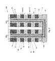
- An array of openings 81may be formed in locations where vertical channels of NAND strings will be subsequently formed.
- the second material 122is selectively etched compared to the first material 121 to form first recesses 62 in the second material 122 (i.e., layers 122 a , 122 b , etc).
- the recesses 62may be formed by selective, isotropic wet or dry etching which selectively etches the second material 122 compared to the first material 121 .
- the depth of each recess 62may be 6 to 100 nm.
- a blocking dielectric 7(also known as an inter-poly dielectric, IPD) is then formed in the openings 81 such that the blocking dielectric coats the sides of the first recesses 62 , resulting in a structure as shown in FIG. 5B .
- the blocking dielectric 7may comprise a silicon oxide layer deposited by conformal atomic layer deposition (ALD) or chemical vapor deposition (CVD).
- ALDconformal atomic layer deposition
- CVDchemical vapor deposition
- Other high-k dielectric materialssuch as hafnium oxide, or multi-layer dielectrics (e.g., ONO) may be used instead or in addition to silicon oxide.
- an insulating capping layere.g., silicon nitride
- the blocking dielectric 7may have a thickness of 6 to 20 nm.
- the blocking dielectric 7comprises a plurality of discrete blocking dielectric segments (e.g., 7 a and 7 b ).
- the blocking dielectric segments 7 a and 7 bare connected to each other by clam-shaped portions of the charge blocking dielectric layer 7 which extend inside the recesses 62 .
- a “clam” shapeis a side cross sectional shape configured similar to an English letter “C”.
- a clam shapehas two segments which extend substantially parallel to each other and to the major surface 100 a of the substrate 100 .
- the two segmentsare connected to each other by a third segment which extends substantially perpendicular to the first two segments and the surface 100 a .
- Each of the three segmentsmay have a straight shape (e.g., a rectangle side cross sectional shape) or a somewhat curved shape (e.g., rising and falling with the curvature of the underlying topography).
- substantially parallelincludes exactly parallel segments as well as segments which deviate by 20 degrees or less from the exact parallel configuration.
- substantially perpendicularincludes exactly perpendicular segments as well as segments which deviate by 20 degrees or less from the exact perpendicular configuration.
- the clam shapepreferably contains an opening bounded by the three segments and having a fourth side open. The opening may be filled by another material or layer.
- a charge storage material 9is formed in the openings 81 and in the first recesses 62 over the blocking dielectric material 7 , resulting in the structure shown in FIG. 5C .
- the charge storage material 9comprises a plurality of charge storage segments (e.g., 9 a and 9 b ) formed between openings in a respective one of the plurality of clam-shaped blocking dielectric segments (e.g., 7 a or 7 b ).
- the charge storage segments 9 a , 9 bare connected to each other by portions of the charge storage material 9 layer which extend inside the recesses 62 .
- the charge storage material 9may comprise a charge storage dielectric material (e.g., silicon nitride).
- the discrete charge storage materialmay comprise a conductive or semiconductor floating gate material (e.g., a metal, metal alloy such as TiN, metal silicide, or heavily doped polysilicon floating gate material). Any desired methods may be used to form the charge storage material 9 , such as ALD or CVD.
- a second sacrificial layer 13is deposited in the clam shaped portion of the charge storage material 9 layer which extends inside the recesses 62 .
- the second sacrificial layercompletely fills the clam shaped portion of the charge storage material layer 9 in the recesses 62 .
- the second sacrificial material 13may be a metal (e.g. titanium, nickel or cobalt) that can form a silicide (e.g.
- the second sacrificial material 13may be formed by filling the openings 81 and the recesses 62 with the second sacrificial material 13 , followed by anisotropic etching to remove the exposed second sacrificial material 13 from the openings 81 such that material 13 remains in the recesses 62 .
- a third sacrificial layer 15is deposited in the opening 81 .
- the third sacrificial layer 15covers the charge storage segments 9 a , 9 b and contacts the second sacrificial material 13 located in the clam shaped portion of the charge storage material layer 9 in recesses 62 .
- the second and third sacrificial materials 13 , 15are then reacted to form a sacrificial compound material 17 .
- the sacrificial compound material 17is formed where the second and third sacrificial material layers 13 , 15 contact each other.
- the second sacrificial material 13is germanium and the third sacrificial material 15 is silicon, these materials can be reacted, such as by heating, to form a silicon-germanium alloy.
- the NAND stringshave a circular cross section as viewed from the top ( FIGS. 1B , 2 B).
- the sacrificial compound material 17may forms SiGe rings around the opening 81 .
- the second sacrificial material 13is a metal such as titanium, cobalt or nickel
- the third sacrificial material 15is silicon
- the second and third sacrificial materials 13 , 15may be heated to form titanium silicide, cobalt silicide or nickel silicide, respectively.
- the heatingmay be any suitable heating, such as rapid thermal annealing at a temperature between 700 and 1100 C, such as 900-1000 C.
- the sacrificial compound material 17 and any of the second sacrificial 13 material remaining in the recesses 62is removed by selective etching. Unreacted portions of the third sacrificial material 15 located adjacent to vertical edges of the control gate material 3 and segments 9 a , 9 b , etc. are not removed.
- the second sacrificial material 13is germanium
- the third sacrificial material 15is silicon
- the sacrificial compound material 17is silicon-germanium.
- Silicon-germanium 17may be selectively etched relative to silicon by wet etching with HNO 3 :HF:CH 3 COOH:H 2 O, HF:HNO 3 :H 2 O, and/or HF:NH 4 F:H 2 O 2 :NH 4 OH.
- the germaniummay be selectively etched relative to silicon nitride 9 by wet-etching with H 2 O 2 or by reactive ion etching (RIE) with BCl 3 /Cl 2 or HBr/Br 2 .
- RIEreactive ion etching
- the portions of the silicon nitride charge storage layer 9 located in the recesses 62 that are not covered by the unreacted portions of third sacrificial material 15may be removed by selective etching.
- Silicon nitridemay be selectively etched relative to silicon or silicon oxide by wet etching with hot H 3 PO 4 :H 2 O or dilute HF at high temperature.
- silicon nitridemay be selectively etched relative to silicon or silicon oxide by RIE with CH x F y based chemistries with x>1, y ⁇ 3 with good selectivity to Si/SiO 2 .
- portions of the charge storage layer 9 located over the vertical edges of the control gate material that are not covered by the unreacted (i.e., masking) portions of third sacrificial material 15may be selectively removed, such that the charge storage segments do not extend into the recesses 62 .
- those portions of the charge storage layer 9 that are covered by the unreacted third sacrificial material 15are not etched.
- some undercut of the unreacted third sacrificial material 15may occur. In this manner, vertically separated, discreet charge storage segments 9 a , 9 b may be formed over the vertical edges of the control gate material 3 .
- unreacted portions of the third sacrificial (e.g., polysilicon) material 15are removed, such as by etching, to expose the vertically separated, discreet charge storage segments 9 a , 9 b , as illustrated in FIG. 5I .
- a tunnel dielectric material 11is deposited in the recesses 62 , over the charge storage segments 9 a , 9 b and in regions between the charge storage segments via the opening 81 .
- the tunnel dielectric material 11may be deposited such that an air gap 19 is formed in the recess 62 . This may be accomplished, for example by depositing the tunnel dielectric material 11 with a chemical vapor deposition (CVD) process to partially fill spaces in the recesses 62 to leave the air gaps 19 in the recesses between adjacent layers of control gate material 3 .
- CVDchemical vapor deposition
- the use of an air gap in the recesses 62reduces capacitance coupling between neighboring world lines in the NAND memory device.
- the tunnel dielectric material 11may deposited, for example, with an atomic layer deposition (ALD) process, to completely fill the spaces in the recesses 62 .
- ALDatomic layer deposition
- the channelmay be formed by depositing channel material 1 , such as a lightly doped or intrinsic polysilicon in the opening 81 . As discussed above, the entire opening 81 may be filled to form the device illustrated in FIGS. 2A and 2B . Alternatively, a layer of channel material 1 may first be deposited in the opening 81 followed by deposition of an insulating fill material 2 to form the device illustrated in FIGS. 1A and 1B . If desired, the channel 1 may be U-shaped as illustrated in FIGS. 3 and 4 .
- channel material 1such as a lightly doped or intrinsic polysilicon
- the third sacrificial material 15may be oxidized after the step illustrated in FIG. 5G . That is, after removing the sacrificial compound 17 and the sacrificial material 13 , the third sacrificial material 15 may be oxidized.
- the oxidationmay comprise exposing material 15 to a dry or wet oxygen containing atmosphere or plasma at an elevated temperature.
- the third sacrificial material 15is polysilicon
- the third sacrificial material 15may be fully oxidized to convert it to silicon oxide 15 a portions.
- material 15 portionsmay be partially oxidized on its surface to form a surface oxide 15 a portions on the polysilicon 15 .
- the oxidation stepforms silicon nitride 9 /silicon oxide 15 a rings around the opening 81 .
- the exposed portions of the silicon nitride layer 9are oxidized to form silicon oxynitride 29 portions in the recesses 62 during the oxidation step. Thereafter, the silicon oxide 15 a portions are removed by selective etching or anisotropic etching to expose the silicon nitride segments 9 a , 9 b .
- the silicon oxynitride 29 portionsare then selectively removed by selective etching, such as by using HF:NH 4 F:H 2 O wet etching medium which etches silicon oxynitride 29 much faster than silicon nitride 9 .
- the processthen proceeds in the same manner as described above and as shown in FIGS. 5I-5J .
- the air gaps 19 and the tunnel dielectric 11are formed in separate steps rather than in the single step described above with respect to FIG. 5I .
- an insulating spacer material 21is formed in the opening 81 prior to removing the third sacrificial material regions 15 .
- the spacer material 21is formed over the third sacrificial material regions 15 and in the recesses 62 to partially fill the spaces in the recesses. This leaves the air gaps 19 as shown in FIG. 7A .
- the spacer material 21may comprise silicon oxide or another insulating material.
- material 21is the same as the tunnel dielectric 11 material.
- the third sacrificial material regions 15 and the spacer material 21are removed from the opening 81 .
- the removalmay take place by a highly anisotropic etch or by lifting off the third sacrificial material regions 15 .
- the tunnel dielectric 11is formed on the exposed charge storage segments 9 a , 9 b separated by the spacer material 21 which partially fills the recesses 62 , as described above with respect to FIG. 5J .
- the channel 1is then formed in the opening 81 over the tunnel dielectric 11 as described above.
- FIGS. 8A-8Gillustrate another alternative embodiment of a vertical NAND with a charge storage region (i.e., charge trapping layer or layer segments described above) containing electrically conductive nanoparticles (also known as nanocrystals or nanodots) embedded in a charge storage dielectric (e.g., electrically insulating) matrix.
- the nanoparticlesmay comprise metal silicide nanoparticles, such as nickel silicide nanoparticles, and the charge storage dielectric matrix may comprise a silicon nitride layer or segments.
- FIG. 8Aillustrates an in-process device at the same stage as FIG. 5B .
- the in-process device in FIG. 8Ashows several openings 81 located throughout the device.
- the blocking dielectric 7is located in the openings 81 , partially filling the recesses 62 .
- a silicon nitride containing layer 91is formed over the blocking dielectric 7 in the openings 81 .
- layer 91may comprise a silicon-rich silicon nitride layer.
- the silicon-rich silicon nitride layer 91has more than 3 silicon atoms for each 4 nitrogen atoms (e.g., Si 3 N 4-x , where 0.1 ⁇ x ⁇ 0.75).
- Layer 91may have a thickness of 1-2 nm. Alternatively, layer 91 may be formed from plural sublayers.
- a thin (e.g., about 1 nm) stoichiometric Si 3 N 4 sublayermay be formed in the openings 81 instead of the silicon-rich silicon nitride layer, followed by formation of a thin (e.g., about 1 nm) sublayer of silicon on the stoichiometric silicon nitride layer.
- an ultra thin layer of a silicide forming metal 93is formed in the openings 81 on layer 91 by CVD, evaporation or another suitable method.
- Layer 93may comprise nickel or another metal, such as cobalt, titanium, tantalum, tungsten, molybdenum, palladium, platinum, etc., which can form a silicide by reaction with silicon.
- Metal layer 93 thicknessis preferably less than 1 nm, such as 0.2-0.5 nm. Such thin layers are usually formed as a discontinuous chain of metal islands.
- layers 91 and 93are annealed to react the metal layer 93 with the silicon in layer 91 to form metal silicide nanoparticles 95 on the silicon nitride layer 91 .
- layers 91 and 93may be annealed at 600-950 C, such as 600-700 C for a sufficient time for the Ni layer 93 to react with the excess silicon in the silicon-rich silicon nitride layer 91 to form nickel silicide nanoparticles 95 located on layer 91 .
- Furnace annealing or rapid thermal annealingmay be used.
- the nanoparticles 95comprise silicides of cobalt, titanium, tantalum, tungsten, molybdenum, palladium, or platinum, rather than nickel silicide.
- An optional wet-cleane.g., wet etch
- one or more additional annealsmay be added so that the nickel silicide nanoparticle islands become well rounded nanocrystals (e.g., single crystal or polycrystalline nanodots) and a desirable NiSi 2 phase of nickel silicide is achieved.
- the nanocrystalsmay have a diameter of 10 nm or less, such as 5 nm or less, such as 0.2 to 2 nm.
- a thin layer (1-2 nm thick) of silicon nitride 97is deposited over the nanoparticles 95 so that the silicide nanoparticles 95 are embedded (e.g., completely embedded) within silicon nitride matrix, as shown in FIG. 8D .
- the silicide nanoparticles 95are embedded between silicon nitride layers 91 and 97 forming the matrix.
- Thisforms a composite charge storage film 99 (also referred to as a charge trapping layer or film) composed of silicon nitride 91 /silicide nanoparticles 95 /silicon nitride 97 .
- the nickel silicide nanoparticles 95are floating within the silicon nitride matrix 91 , 97 of the charge storage film 99 , and preferably are not in contact with adjacent blocking oxide dielectric 7 or the tunneling oxide dielectric 11 .
- layer 97may comprise a silicon-rich silicon nitride layer in which case, the silicide nanoparticles 95 may be formed within the charge storage film 99 , by thermal annealing of a sandwich structure comprising of layers 91 , 93 and 97 .
- the electrically conductive nanoparticlesare embedded in an electrically insulating oxide layer. This means that the nanoparticles rather than the surrounding oxide layers trap the charge.
- a charge trapping dielectric matrixsuch as silicon nitride
- both the nanoparticles 95 and the dielectric matrix 91 , 97can be used to trap charge in film 99 .
- the vertical NAND cell with composite film 99may exhibit better reliability and charge trapping performance than a comparable cell with a single silicon nitride charge storage layer 9 .
- the processcan proceed as shown in FIGS. 5C-5J , 6 and/or 7 A- 7 B, and as described above.
- the composite silicon nitride/silicide/silicon nitride charge storage film 99may be used instead of the single silicon nitride charge storage layer 9 shown in FIG. 5C and then patterned into composite charge storage segments as shown in FIG. 5H .
- the charge storage region of the vertical NAND stringcomprises the continuous composite film 99 (e.g., silicide nanoparticles in the charge storage dielectric matrix) instead of discrete segments shown in FIG. 5H .
- the recesses 62may be pinched-off (i.e., filled) by the silicon nitride layer 97 during deposition of layer 97 or the recesses 62 may be left partially unfilled.
- the tunnel dielectric 11is deposited into the openings 81 in contact with the composite charge storage film 99 .
- the tunnel dielectric 11may comprise a silicon oxide layer or an ONO film having any suitable thickness, such as 4-15 nm. If the recesses 62 are completely filled with layer 97 , then the tunnel dielectric 11 may have substantially straight sidewalls.
- the tunnel dielectric 11may completely fill the recesses 62 or partially fill the recesses 62 to leave the air gaps 19 in the recesses (as shown in FIG. 5I or 7 A).
- a channel semiconductor layer 101is deposited over the device to fill the openings 81 .
- Layer 101may be lightly doped n-type or p-type polysilicon or another material, as described above.
- layer 101is etched back from the top to form the pillar shaped (or U-shaped) channels 1 in the openings 81 .
- the space between the channels 1is filled with a gap fill insulating layer 103 , such as silicon oxide or another material.
- Layer 103may be formed by depositing an oxide layer over the channels followed by etch back or chemical mechanical polishing to form a planar top surface expositing the top surfaces of the channels 1 .
- the channelsare then connected to source and drain electrodes as shown in FIGS. 1-4 , the select gate electrodes (not shown for clarity) are connected to select gate contacts and the control gate electrodes 3 are connected to word line contacts as known in the art.
Landscapes
- Engineering & Computer Science (AREA)
- Physics & Mathematics (AREA)
- Condensed Matter Physics & Semiconductors (AREA)
- General Physics & Mathematics (AREA)
- Manufacturing & Machinery (AREA)
- Computer Hardware Design (AREA)
- Microelectronics & Electronic Packaging (AREA)
- Power Engineering (AREA)
- Semiconductor Memories (AREA)
- Non-Volatile Memory (AREA)
Abstract
Description
- The present invention relates generally to the field of semiconductor devices and specifically to three dimensional vertical NAND strings and other three dimensional devices and methods of making thereof.
- Three dimensional vertical NAND strings are disclosed in an article by T. Endoh, et. al., titled “Novel Ultra High Density Memory With A Stacked-Surrounding Gate Transistor (S-SGT) Structured Cell”, IEDM Proc. (2001) 33-36. However, this NAND string provides only one bit per cell. Furthermore, the active regions of the NAND string is formed by a relatively difficult and time consuming process involving repeated formation of sidewall spacers and etching of a portion of the substrate, which results in a roughly conical active region shape.
- An embodiment relates to a method of making a device including forming a stack of alternating layers of a first material and a second material over a substrate. The first material includes a conductive or semiconductor control gate material and the second material includes a first sacrificial material. The method also includes etching the stack to form an opening in the stack, selectively removing the second material through the opening to form recesses, forming a blocking dielectric layer in the recesses to partially fill the recesses, the blocking dielectric layer located on surfaces of the control gate material and forming a charge storage material layer over the blocking dielectric such that the charge storage material layer partially fills the recesses and is located over the blocking dielectric layer. The method also includes filling the recesses with a second sacrificial material, at least partially filling the opening with a third sacrificial material, such that the third sacrificial material contacts the second sacrificial material and reacting the second and third sacrificial materials to form a sacrificial compound material comprising the second and third sacrificial materials where the second and third sacrificial material layers contact each other. The method also includes, selectively removing the sacrificial compound material and any second sacrificial material remaining in the recesses while leaving unreacted portions of the third sacrificial material located adjacent to vertical edges of the control gate material and selectively removing portions of the charge storage material layer located in the recesses that are not covered by the unreacted portion of third sacrificial material located over the vertical edges of the control gate material, thereby forming vertically separated charge storage segments over the vertical edges of the control gate material.
- Another embodiment relates to a monolithic three dimensional NAND string including a semiconductor channel, at least one end portion of the semiconductor channel extending substantially perpendicular to a major surface of a substrate. The string also includes a plurality of control gate electrodes having a strip shape with major surfaces extending substantially parallel to the major surface of the substrate. The plurality of control gate electrodes include at least a first control gate electrode located in a first device level and a second control gate electrode located in a second device level located over the major surface of the substrate and below the first device level. The first control gate electrode is separated from the second control gate electrode by an air gap located substantially between the major surfaces of the first and second control gate electrodes. The string also includes a blocking dielectric layer located in contact with the plurality of control gate electrodes and a plurality of spaced apart charge storage segments. The plurality of spaced apart charge storage segments include at least a first spaced apart charge storage segment located in the first device level and a second spaced apart charge storage segment located in the second device level. The string also includes a tunnel dielectric layer located between each one of the plurality of the spaced apart charge storage segments and the semiconductor channel.
- Another embodiment relates to a monolithic three dimensional NAND string including a semiconductor channel, at least one end portion of the semiconductor channel extending substantially perpendicular to a major surface of a substrate and a plurality of control gate electrodes having a strip shape with major surfaces extending substantially parallel to the major surface of the substrate. The plurality of control gate electrodes comprise at least a first control gate electrode located in a first device level and a second control gate electrode located in a second device level located over the major surface of the substrate and below the first device level. The string also includes a blocking dielectric layer located in contact with the plurality of control gate electrodes, a charge storage region comprising metal silicide nanoparticles embedded in a charge storage dielectric matrix, and a tunnel dielectric layer located between the charge storage region and the semiconductor channel.
- Another embodiment relates to a method of making a vertical, monolithic three dimensional NAND string, comprising forming a stack of alternating layers of a first material and a second material over a substrate, wherein the first material comprises a conductive or semiconductor control gate material, etching the stack to form an opening in the stack, forming a blocking dielectric layer in the opening, the blocking dielectric layer located on surfaces of the control gate material, forming a charge storage region comprising metal silicide nanoparticles embedded in a charge storage dielectric matrix in the opening over the blocking dielectric layer, forming a tunnel dielectric layer in the opening, and forming a semiconductor channel layer in the opening over the tunnel dielectric layer.
FIGS. 1A-1B are respectively side cross sectional and top cross sectional views of a NAND string of one embodiment.FIG. 1A is a side cross sectional view of the device along line Y-Y′ inFIG. 1B , whileFIG. 1B is a side cross sectional view of the device along line X-X′ inFIG. 1A .FIGS. 2A-2B are respectively side cross sectional and top cross sectional views of a NAND string of another embodiment.FIG. 2A is a side cross sectional view of the device along line Y-Y′ inFIG. 2B , whileFIG. 2B is a side cross sectional view of the device along line X-X′ inFIG. 2A .FIG. 3 is side cross sectional view of a NAND string of an embodiment with a U-shaped channel.FIG. 4 is side cross sectional view of a NAND string of another embodiment with a U-shaped channel.FIGS. 5A-5J ,6 and7A-7B are side cross sectional views illustrating embodiments of methods of making the NAND strings illustrated inFIGS. 1-4 .FIGS. 8A-8G are side cross sectional views illustrating alternative embodiments of methods of making vertical NAND strings.- The embodiments of the invention provide a monolithic, three dimensional array of memory devices, such as an array of vertical NAND strings. The NAND strings are vertically oriented, such that at least one memory cell is located over another memory cell. The array allows vertical scaling of NAND devices to provide a higher density of memory cells per unit area of silicon or other semiconductor material.
- A monolithic three dimensional memory array is one in which multiple memory levels are formed above a single substrate, such as a semiconductor wafer, with no intervening substrates. The term “monolithic” means that layers of each level of the array are directly deposited on the layers of each underlying level of the array. In contrast, two dimensional arrays may be formed separately and then packaged together to form a non-monolithic memory device. For example, non-monolithic stacked memories have been constructed by forming memory levels on separate substrates and adhering the memory levels atop each other, as in Leedy, U.S. Pat. No. 5,915,167, titled “Three Dimensional Structure Memory.” The substrates may be thinned or removed from the memory levels before bonding, but as the memory levels are initially formed over separate substrates, such memories are not true monolithic three dimensional memory arrays.
- In some embodiments, the monolithic three
dimensional NAND string 180 comprises asemiconductor channel 1 having at least one end portion extending substantially perpendicular to amajor surface 100aof asubstrate 100, as shown inFIGS. 1A and 2A . For example, thesemiconductor channel 1 may have a pillar shape and the entire pillar-shaped semiconductor channel extends substantially perpendicularly to the major surface of thesubstrate 100, as shown inFIGS. 1A and 2A . In these embodiments, the source/drain electrodes of the device can include alower electrode 102 provided below thesemiconductor channel 1 and anupper electrode 202 formed over thesemiconductor channel 1, as shown inFIGS. 1A and 2A . Alternatively, thesemiconductor channel 1 may have a U-shaped pipe shape, as shown inFIGS. 3 and 4 . The twowing portions major surface 100aof thesubstrate 100, and a connectingportion 1cof the U-shaped pipeshape semiconductor channel 1 connects the twowing portions major surface 100aof thesubstrate 100. In these embodiments, one of the source ordrain electrodes 2021contacts the first wing portion of the semiconductor channel from above, and another one of a source ordrain electrodes 2022contacts the second wing portion of thesemiconductor channel 1 from above. An optional body contact electrode (not shown) may be disposed in thesubstrate 100 to provide body contact to the connecting portion of thesemiconductor channel 1 from below. The NAND string's select or access transistors are not shown inFIGS. 1-4 for clarity. - In some embodiments, the
semiconductor channel 1 may be a filled feature, as shown inFIGS. 2A-2B and4. In some other embodiments, thesemiconductor channel 1 may be hollow, for example a hollow cylinder filled with an insulatingfill material 2, as shown inFIGS. 1A-1B and3. In these embodiments, and an insulatingfill material 2 may be formed to fill the hollow part surrounded by thesemiconductor channel 1. - The
substrate 100 can be any semiconducting substrate known in the art, such as monocrystalline silicon, IV-IV compounds such as silicon-germanium or silicon-germanium-carbon, III-V compounds, II-VI compounds, epitaxial layers over such substrates, or any other semiconducting or non-semiconducting material, such as silicon oxide, glass, plastic, metal or ceramic substrate. Thesubstrate 100 may include integrated circuits fabricated thereon, such as driver circuits for a memory device. - Any suitable semiconductor materials can be used for
semiconductor channel 1, for example silicon, germanium, silicon germanium, or other compound semiconductor materials, such as III-V, II-VI, or conductive or semiconductive oxides, etc. materials. The semiconductor material may be amorphous, polycrystalline or single crystal. The semiconductor channel material may be formed by any suitable deposition methods. For example, in one embodiment, the semiconductor channel material is deposited by low pressure chemical vapor deposition (LPCVD). In some other embodiments, the semiconductor channel material may be a recrystallized polycrystalline semiconductor material formed by recrystallizing an initially deposited amorphous semiconductor material. - The insulating
fill material 2 may comprise any electrically insulating material, such as silicon oxide, silicon nitride, silicon oxynitride, or other high-k insulating materials. - The monolithic three dimensional NAND string further comprise a plurality of
control gate electrodes 3, as shown inFIGS. 1A-1B ,2A-2B, and3-4. Thecontrol gate electrodes 3 may comprise a portion having a strip shape extending substantially parallel to themajor surface 100aof thesubstrate 100. The plurality ofcontrol gate electrodes 3 comprise at least a firstcontrol gate electrode 3alocated in a first device level (e.g., device level A) and a secondcontrol gate electrode 3blocated in a second device level (e.g., device level B) located over themajor surface 100aof thesubstrate 100 and below the device level A. The control gate material may comprise any one or more suitable conductive or semiconductor control gate material known in the art, such as doped polysilicon, tungsten, copper, aluminum, tantalum, titanium, cobalt, titanium nitride or alloys thereof. For example, in some embodiments, polysilicon is preferred to allow easy processing. - A blocking
dielectric 7 is located adjacent to the control gate(s)3 and may surround thecontrol gate 3. The blockingdielectric 7 may comprise a plurality of blocking dielectric segments located in contact with a respective one of the plurality ofcontrol gate electrodes 3, for example afirst dielectric segment 7alocated in device level A and asecond dielectric segment 7blocated in device level B are in contact withcontrol electrodes FIGS. 3 and 4 . - The monolithic three dimensional NAND string also comprise a plurality of discrete
charge storage segments 9 located between the blockingdielectric 7 and thechannel 1. Similarly, the plurality of discretecharge storage segments 9 comprise at least a first discretecharge storage segment 9alocated in the device level A and a second discretecharge storage segment 9blocated in the device level B, as shown inFIGS. 3 and 4 . - The tunnel dielectric11 of the monolithic three dimensional NAND string is located between each one of the plurality of the discrete
charge storage segments 9 and thesemiconductor channel 1. - The blocking
dielectric 7 and thetunnel dielectric 11 may be independently selected from any one or more same or different electrically insulating materials, such as silicon oxide, silicon nitride, silicon oxynitride, or other high-k insulating materials. The blockingdielectric 7 and/or thetunnel dielectric 11 may include multiple layers of silicon oxide, silicon nitride and/or silicon oxynitride (e.g., ONO layers). - The discrete
charge storage segments 9 may comprise a conductive (e.g., metal or metal alloy such as titanium, platinum, ruthenium, titanium nitride, hafnium nitride, tantalum nitride, zirconium nitride, or a metal silicide such as titanium silicide, nickel silicide, cobalt silicide, or a combination thereof) or semiconductor (e.g., polysilicon) floating gate, conductive nanoparticles, or a discrete charge storage dielectric (e.g., silicon nitride or another dielectric) feature. For example, in some embodiments, the discretecharge storage segments 9 are discrete charge storage dielectric features, each of which comprises a nitride feature adjacent therespective blocking dielectric 7, where the siliconoxide blocking dielectric 7, thenitride feature 9 and the siliconoxide tunnel dielectric 11 form oxide-nitride-oxide discrete charge storage structures of the NAND string. FIGS. 5A-5J illustrate a method of making a NAND string according to a first embodiment of the invention.- Referring to
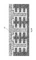
FIG. 5A , astack 120 of alternating layers121 (121a,121b, etc.) and122 (122a,122betc.) are formed over the major surface of thesubstrate 100.Layers 121,122 may be deposited over the substrate by any suitable deposition method, such as sputtering, CVD, MBE, etc. Thelayers 121,122 may be 6 to 100 nm thick. - In this embodiment, the first layers121 comprise a first conductive (e.g., metal or metal alloy) or semiconductor (e.g., heavily doped n+ or p+ polysilicon) control gate material, and the
second layers 122 comprise a first sacrificial material, such as intrinsic polysilicon or an insulating material (e.g., silicon nitride, silicon oxide, etc.). The term heavily doped includes semiconductor materials doped n-type or p-type to a concentration of above 1018cm−3. In contrast, lightly doped semiconductor materials have a doping concentration below 1018cm−3and intrinsic semiconductor materials have a doping concentration below 1015cm−3. - The deposition of
layers 121,122 is followed by etching thestack 120 to form at least oneopening 81 in thestack 120. An array ofopenings 81 may be formed in locations where vertical channels of NAND strings will be subsequently formed. - Next, the
second material 122 is selectively etched compared to the first material121 to form first recesses62 in the second material122 (i.e., layers122a,122b, etc). Therecesses 62 may be formed by selective, isotropic wet or dry etching which selectively etches thesecond material 122 compared to the first material121. The depth of eachrecess 62 may be 6 to 100 nm. - A blocking dielectric7 (also known as an inter-poly dielectric, IPD) is then formed in the
openings 81 such that the blocking dielectric coats the sides of thefirst recesses 62, resulting in a structure as shown inFIG. 5B . The blockingdielectric 7 may comprise a silicon oxide layer deposited by conformal atomic layer deposition (ALD) or chemical vapor deposition (CVD). Other high-k dielectric materials, such as hafnium oxide, or multi-layer dielectrics (e.g., ONO) may be used instead or in addition to silicon oxide. Optionally, an insulating capping layer (e.g., silicon nitride) may be deposited into the openings before the blockingdielectric 7 and may comprise a back portion of a multi-layer blocking dielectric. The blockingdielectric 7 may have a thickness of 6 to 20 nm. The blockingdielectric 7 comprises a plurality of discrete blocking dielectric segments (e.g.,7aand7b). The blockingdielectric segments dielectric layer 7 which extend inside therecesses 62. - As used herein a “clam” shape is a side cross sectional shape configured similar to an English letter “C”. A clam shape has two segments which extend substantially parallel to each other and to the
major surface 100aof thesubstrate 100. The two segments are connected to each other by a third segment which extends substantially perpendicular to the first two segments and thesurface 100a. Each of the three segments may have a straight shape (e.g., a rectangle side cross sectional shape) or a somewhat curved shape (e.g., rising and falling with the curvature of the underlying topography). The term substantially parallel includes exactly parallel segments as well as segments which deviate by 20 degrees or less from the exact parallel configuration. The term substantially perpendicular includes exactly perpendicular segments as well as segments which deviate by 20 degrees or less from the exact perpendicular configuration. The clam shape preferably contains an opening bounded by the three segments and having a fourth side open. The opening may be filled by another material or layer. - A
charge storage material 9 is formed in theopenings 81 and in thefirst recesses 62 over the blockingdielectric material 7, resulting in the structure shown inFIG. 5C . Thecharge storage material 9 comprises a plurality of charge storage segments (e.g.,9aand9b) formed between openings in a respective one of the plurality of clam-shaped blocking dielectric segments (e.g.,7aor7b). Thecharge storage segments charge storage material 9 layer which extend inside therecesses 62. - As explained above, in some embodiments, the
charge storage material 9 may comprise a charge storage dielectric material (e.g., silicon nitride). Alternatively, the discrete charge storage material may comprise a conductive or semiconductor floating gate material (e.g., a metal, metal alloy such as TiN, metal silicide, or heavily doped polysilicon floating gate material). Any desired methods may be used to form thecharge storage material 9, such as ALD or CVD. - In the next step of this embodiment of the method, illustrated in
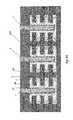
FIG. 5D , a secondsacrificial layer 13 is deposited in the clam shaped portion of thecharge storage material 9 layer which extends inside therecesses 62. Preferably, the second sacrificial layer completely fills the clam shaped portion of the chargestorage material layer 9 in therecesses 62. The secondsacrificial material 13 may be a metal (e.g. titanium, nickel or cobalt) that can form a silicide (e.g. titanium, nickel or cobalt silicide) or a semiconducting material that forms a semiconducting alloy (e.g., Ge which may be alloyed with Si or C to form SiGe or GeC) that may be selectively etched relative to the metal or constituent semiconducting elements. The secondsacrificial material 13 may be formed by filling theopenings 81 and therecesses 62 with the secondsacrificial material 13, followed by anisotropic etching to remove the exposed secondsacrificial material 13 from theopenings 81 such thatmaterial 13 remains in therecesses 62. - Next, as illustrated in
FIG. 5E , a thirdsacrificial layer 15 is deposited in theopening 81. The thirdsacrificial layer 15 covers thecharge storage segments sacrificial material 13 located in the clam shaped portion of the chargestorage material layer 9 inrecesses 62. - As illustrated in
FIG. 5F , the second and thirdsacrificial materials sacrificial compound material 17. Thesacrificial compound material 17 is formed where the second and third sacrificial material layers13,15 contact each other. For example, if the secondsacrificial material 13 is germanium and the thirdsacrificial material 15 is silicon, these materials can be reacted, such as by heating, to form a silicon-germanium alloy. In an embodiment, the NAND strings have a circular cross section as viewed from the top (FIGS. 1B ,2B). Thesacrificial compound material 17 may forms SiGe rings around theopening 81. Alternatively, if the secondsacrificial material 13 is a metal such as titanium, cobalt or nickel, and the thirdsacrificial material 15 is silicon, then the second and thirdsacrificial materials - Next, as illustrated in
FIG. 5G , thesacrificial compound material 17 and any of the second sacrificial13 material remaining in therecesses 62 is removed by selective etching. Unreacted portions of the thirdsacrificial material 15 located adjacent to vertical edges of thecontrol gate material 3 andsegments sacrificial material 13 is germanium, the thirdsacrificial material 15 is silicon and thesacrificial compound material 17 is silicon-germanium. Silicon-germanium 17 may be selectively etched relative to silicon by wet etching with HNO3:HF:CH3COOH:H2O, HF:HNO3:H2O, and/or HF:NH4F:H2O2:NH4OH. The germanium may be selectively etched relative tosilicon nitride 9 by wet-etching with H2O2or by reactive ion etching (RIE) with BCl3/Cl2or HBr/Br2. - As illustrated in
FIG. 5H , the portions of the silicon nitridecharge storage layer 9 located in therecesses 62 that are not covered by the unreacted portions of thirdsacrificial material 15 may be removed by selective etching. Silicon nitride may be selectively etched relative to silicon or silicon oxide by wet etching with hot H3PO4:H2O or dilute HF at high temperature. Alternatively, silicon nitride may be selectively etched relative to silicon or silicon oxide by RIE with CHxFybased chemistries with x>1, y<3 with good selectivity to Si/SiO2. - Additionally, portions of the
charge storage layer 9 located over the vertical edges of the control gate material that are not covered by the unreacted (i.e., masking) portions of thirdsacrificial material 15 may be selectively removed, such that the charge storage segments do not extend into therecesses 62. However, those portions of thecharge storage layer 9 that are covered by the unreacted thirdsacrificial material 15 are not etched. However, as illustrated inFIG. 5H , some undercut of the unreacted thirdsacrificial material 15 may occur. In this manner, vertically separated, discreetcharge storage segments control gate material 3. Thus, selectively removing portions of the charge storage material (e.g., silicon nitride)layer 9 located in therecesses 62 that are not covered by the unreacted portions of the third sacrificial (e.g., polysilicon)material 15forms silicon nitride 9/polysilicon 15 rings around theopening 81. - In the next step, unreacted portions of the third sacrificial (e.g., polysilicon)
material 15 are removed, such as by etching, to expose the vertically separated, discreetcharge storage segments FIG. 5I . Then, atunnel dielectric material 11 is deposited in therecesses 62, over thecharge storage segments opening 81. - Optionally, in an embodiment, the
tunnel dielectric material 11 may be deposited such that anair gap 19 is formed in therecess 62. This may be accomplished, for example by depositing thetunnel dielectric material 11 with a chemical vapor deposition (CVD) process to partially fill spaces in therecesses 62 to leave theair gaps 19 in the recesses between adjacent layers ofcontrol gate material 3. The use of an air gap in therecesses 62 reduces capacitance coupling between neighboring world lines in the NAND memory device. In those embodiments in which anair gap 19 is not desired, thetunnel dielectric material 11 may deposited, for example, with an atomic layer deposition (ALD) process, to completely fill the spaces in therecesses 62. - As illustrated in
FIG. 5J , the channel may be formed by depositingchannel material 1, such as a lightly doped or intrinsic polysilicon in theopening 81. As discussed above, theentire opening 81 may be filled to form the device illustrated inFIGS. 2A and 2B . Alternatively, a layer ofchannel material 1 may first be deposited in theopening 81 followed by deposition of an insulatingfill material 2 to form the device illustrated inFIGS. 1A and 1B . If desired, thechannel 1 may be U-shaped as illustrated inFIGS. 3 and 4 . - In an alternative second embodiment illustrated in
FIG. 6 , the thirdsacrificial material 15 may be oxidized after the step illustrated inFIG. 5G . That is, after removing thesacrificial compound 17 and thesacrificial material 13, the thirdsacrificial material 15 may be oxidized. The oxidation may comprise exposingmaterial 15 to a dry or wet oxygen containing atmosphere or plasma at an elevated temperature. For example, when the thirdsacrificial material 15 is polysilicon, the thirdsacrificial material 15 may be fully oxidized to convert it tosilicon oxide 15aportions. Alternatively,material 15 portions may be partially oxidized on its surface to form asurface oxide 15aportions on thepolysilicon 15. The oxidation step formssilicon nitride 9/silicon oxide 15arings around theopening 81. - When the
charge storage layer 9 is made of silicon nitride, the exposed portions of thesilicon nitride layer 9 are oxidized to formsilicon oxynitride 29 portions in therecesses 62 during the oxidation step. Thereafter, thesilicon oxide 15aportions are removed by selective etching or anisotropic etching to expose thesilicon nitride segments silicon oxynitride 29 much faster thansilicon nitride 9. The process then proceeds in the same manner as described above and as shown inFIGS. 5I-5J . - In an alternative third embodiment illustrated in
FIGS. 7A and 7B , theair gaps 19 and thetunnel dielectric 11 are formed in separate steps rather than in the single step described above with respect toFIG. 5I . After thesacrificial compound material 17 is removed as described above with respect toFIG. 5G , an insulatingspacer material 21 is formed in theopening 81 prior to removing the thirdsacrificial material regions 15. Thespacer material 21 is formed over the thirdsacrificial material regions 15 and in therecesses 62 to partially fill the spaces in the recesses. This leaves theair gaps 19 as shown inFIG. 7A . Thespacer material 21 may comprise silicon oxide or another insulating material. Preferably,material 21 is the same as thetunnel dielectric 11 material. - Thereafter, the third
sacrificial material regions 15 and thespacer material 21 are removed from theopening 81. The removal may take place by a highly anisotropic etch or by lifting off the thirdsacrificial material regions 15. This leaves therecesses 62 partially filled with thespacer material 21 having theair gaps 19, as shown inFIG. 7B . Thereafter, thetunnel dielectric 11 is formed on the exposedcharge storage segments spacer material 21 which partially fills therecesses 62, as described above with respect toFIG. 5J . Thechannel 1 is then formed in theopening 81 over thetunnel dielectric 11 as described above. FIGS. 8A-8G illustrate another alternative embodiment of a vertical NAND with a charge storage region (i.e., charge trapping layer or layer segments described above) containing electrically conductive nanoparticles (also known as nanocrystals or nanodots) embedded in a charge storage dielectric (e.g., electrically insulating) matrix. The nanoparticles may comprise metal silicide nanoparticles, such as nickel silicide nanoparticles, and the charge storage dielectric matrix may comprise a silicon nitride layer or segments.- The initial process steps may be the same as the steps shown in
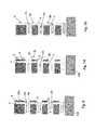
FIGS. 5A and 5B and described above.FIG. 8A illustrates an in-process device at the same stage asFIG. 5B . The in-process device inFIG. 8A showsseveral openings 81 located throughout the device. The blockingdielectric 7 is located in theopenings 81, partially filling therecesses 62. - Next, as shown in
FIG. 8B , a siliconnitride containing layer 91 is formed over the blocking dielectric7 in theopenings 81. In one embodiment,layer 91 may comprise a silicon-rich silicon nitride layer. The silicon-richsilicon nitride layer 91 has more than 3 silicon atoms for each 4 nitrogen atoms (e.g., Si3N4-x, where 0.1<x<0.75).Layer 91 may have a thickness of 1-2 nm. Alternatively,layer 91 may be formed from plural sublayers. For example, a thin (e.g., about 1 nm) stoichiometric Si3N4sublayer may be formed in theopenings 81 instead of the silicon-rich silicon nitride layer, followed by formation of a thin (e.g., about 1 nm) sublayer of silicon on the stoichiometric silicon nitride layer. This formslayer 91 with two sublayers, with the silicon sublayer being exposed in theopenings 81. - Then, an ultra thin layer of a
silicide forming metal 93 is formed in theopenings 81 onlayer 91 by CVD, evaporation or another suitable method.Layer 93 may comprise nickel or another metal, such as cobalt, titanium, tantalum, tungsten, molybdenum, palladium, platinum, etc., which can form a silicide by reaction with silicon.Metal layer 93 thickness is preferably less than 1 nm, such as 0.2-0.5 nm. Such thin layers are usually formed as a discontinuous chain of metal islands. - Next, as shown in
FIG. 8C , layers91 and93 are annealed to react themetal layer 93 with the silicon inlayer 91 to formmetal silicide nanoparticles 95 on thesilicon nitride layer 91. For example, layers91 and93 may be annealed at 600-950 C, such as 600-700 C for a sufficient time for theNi layer 93 to react with the excess silicon in the silicon-richsilicon nitride layer 91 to formnickel silicide nanoparticles 95 located onlayer 91. Furnace annealing or rapid thermal annealing may be used. - If metals other than nickel are used, such as cobalt, titanium, tantalum, tungsten, molybdenum, palladium, or platinum, then the
nanoparticles 95 comprise silicides of cobalt, titanium, tantalum, tungsten, molybdenum, palladium, or platinum, rather than nickel silicide. An optional wet-clean (e.g., wet etch) may be added to remove unreacted Ni if all Ni inlayer 93 is not consumed in forming thesilicide nanoparticles 95. Optionally, one or more additional anneals (e.g., furnace or rapid thermal anneals) may be added so that the nickel silicide nanoparticle islands become well rounded nanocrystals (e.g., single crystal or polycrystalline nanodots) and a desirable NiSi2phase of nickel silicide is achieved. The nanocrystals may have a diameter of 10 nm or less, such as 5 nm or less, such as 0.2 to 2 nm. - After nickel silicide nanoparticle formation, a thin layer (1-2 nm thick) of
silicon nitride 97 is deposited over thenanoparticles 95 so that thesilicide nanoparticles 95 are embedded (e.g., completely embedded) within silicon nitride matrix, as shown inFIG. 8D . In other words, thesilicide nanoparticles 95 are embedded between silicon nitride layers91 and97 forming the matrix. This forms a composite charge storage film99 (also referred to as a charge trapping layer or film) composed ofsilicon nitride 91/silicide nanoparticles 95/silicon nitride 97. Thenickel silicide nanoparticles 95 are floating within thesilicon nitride matrix blocking oxide dielectric 7 or thetunneling oxide dielectric 11. In another embodiment,layer 97 may comprise a silicon-rich silicon nitride layer in which case, thesilicide nanoparticles 95 may be formed within the charge storage film99, by thermal annealing of a sandwich structure comprising oflayers - In some prior art references (see e.g., Yoo-Sung Jang, et al.,
IEEE TRANSACTIONS ON ELECTRON DEVICES , Vol. 56, No. 12, p. 3236, December 2009), the electrically conductive nanoparticles are embedded in an electrically insulating oxide layer. This means that the nanoparticles rather than the surrounding oxide layers trap the charge. In contrast, as shown inFIG. 8D , when the nanoparticles are embedded in a charge trapping dielectric matrix, such as silicon nitride, then both thenanoparticles 95 and thedielectric matrix charge storage layer 9. - After the step shown in
FIG. 8D , the process can proceed as shown inFIGS. 5C-5J ,6 and/or7A-7B, and as described above. In other words, the composite silicon nitride/silicide/silicon nitride charge storage film99 may be used instead of the single silicon nitridecharge storage layer 9 shown inFIG. 5C and then patterned into composite charge storage segments as shown inFIG. 5H . - Alternatively, the use of the second and third
sacrificial materials sacrificial compound material 17 shown inFIGS. 5D-5F may be omitted. Instead, the process after the formation of film99 may proceed as shown inFIGS. 8E-8G and as described below. In this embodiment, the charge storage region of the vertical NAND string comprises the continuous composite film99 (e.g., silicide nanoparticles in the charge storage dielectric matrix) instead of discrete segments shown inFIG. 5H . - As shown in
FIG. 8E , therecesses 62 may be pinched-off (i.e., filled) by thesilicon nitride layer 97 during deposition oflayer 97 or therecesses 62 may be left partially unfilled. After formation oflayer 97, thetunnel dielectric 11 is deposited into theopenings 81 in contact with the composite charge storage film99. Thetunnel dielectric 11 may comprise a silicon oxide layer or an ONO film having any suitable thickness, such as 4-15 nm. If therecesses 62 are completely filled withlayer 97, then thetunnel dielectric 11 may have substantially straight sidewalls. If therecesses 62 are not completely filled withlayer 97, then thetunnel dielectric 11 may completely fill therecesses 62 or partially fill therecesses 62 to leave theair gaps 19 in the recesses (as shown inFIG. 5I or7A). - Next, as shown in
FIG. 8F , achannel semiconductor layer 101 is deposited over the device to fill theopenings 81.Layer 101 may be lightly doped n-type or p-type polysilicon or another material, as described above. - Finally, as shown in
FIG. 8G ,layer 101 is etched back from the top to form the pillar shaped (or U-shaped)channels 1 in theopenings 81. The space between thechannels 1 is filled with a gapfill insulating layer 103, such as silicon oxide or another material.Layer 103 may be formed by depositing an oxide layer over the channels followed by etch back or chemical mechanical polishing to form a planar top surface expositing the top surfaces of thechannels 1. The channels are then connected to source and drain electrodes as shown inFIGS. 1-4 , the select gate electrodes (not shown for clarity) are connected to select gate contacts and thecontrol gate electrodes 3 are connected to word line contacts as known in the art. - Although the foregoing refers to particular preferred embodiments, it will be understood that the invention is not so limited. It will occur to those of ordinary skill in the art that various modifications may be made to the disclosed embodiments and that such modifications are intended to be within the scope of the invention. All of the publications, patent applications and patents cited herein are incorporated herein by reference in their entirety.
Claims (22)
Priority Applications (5)
| Application Number | Priority Date | Filing Date | Title |
|---|---|---|---|
| US13/544,328US8658499B2 (en) | 2012-07-09 | 2012-07-09 | Three dimensional NAND device and method of charge trap layer separation and floating gate formation in the NAND device |
| PCT/US2013/048508WO2014011415A1 (en) | 2012-07-09 | 2013-06-28 | Three dimensional nand device and method of charge trap layer separation and floating gate formation in the nand device |
| CN201380042237.XACN104541370A (en) | 2012-07-09 | 2013-06-28 | Three dimensional NAND device and method of charge trap layer separation and floating gate formation in the NAND device |
| US14/166,162US8933501B2 (en) | 2012-07-09 | 2014-01-28 | Three dimensional NAND device and method of charge trap layer separation and floating gate formation in the NAND device |
| US14/546,671US9093321B2 (en) | 2012-07-09 | 2014-11-18 | Three dimensional NAND device and method of charge trap layer separation and floating gate formation in the NAND device |
Applications Claiming Priority (1)
| Application Number | Priority Date | Filing Date | Title |
|---|---|---|---|
| US13/544,328US8658499B2 (en) | 2012-07-09 | 2012-07-09 | Three dimensional NAND device and method of charge trap layer separation and floating gate formation in the NAND device |
Related Child Applications (1)
| Application Number | Title | Priority Date | Filing Date |
|---|---|---|---|
| US14/166,162DivisionUS8933501B2 (en) | 2012-07-09 | 2014-01-28 | Three dimensional NAND device and method of charge trap layer separation and floating gate formation in the NAND device |
Publications (2)
| Publication Number | Publication Date |
|---|---|
| US20140008714A1true US20140008714A1 (en) | 2014-01-09 |
| US8658499B2 US8658499B2 (en) | 2014-02-25 |
Family
ID=48747810
Family Applications (3)
| Application Number | Title | Priority Date | Filing Date |
|---|---|---|---|
| US13/544,328ActiveUS8658499B2 (en) | 2012-07-09 | 2012-07-09 | Three dimensional NAND device and method of charge trap layer separation and floating gate formation in the NAND device |
| US14/166,162ActiveUS8933501B2 (en) | 2012-07-09 | 2014-01-28 | Three dimensional NAND device and method of charge trap layer separation and floating gate formation in the NAND device |
| US14/546,671ActiveUS9093321B2 (en) | 2012-07-09 | 2014-11-18 | Three dimensional NAND device and method of charge trap layer separation and floating gate formation in the NAND device |
Family Applications After (2)
| Application Number | Title | Priority Date | Filing Date |
|---|---|---|---|
| US14/166,162ActiveUS8933501B2 (en) | 2012-07-09 | 2014-01-28 | Three dimensional NAND device and method of charge trap layer separation and floating gate formation in the NAND device |
| US14/546,671ActiveUS9093321B2 (en) | 2012-07-09 | 2014-11-18 | Three dimensional NAND device and method of charge trap layer separation and floating gate formation in the NAND device |
Country Status (3)
| Country | Link |
|---|---|
| US (3) | US8658499B2 (en) |
| CN (1) | CN104541370A (en) |
| WO (1) | WO2014011415A1 (en) |
Cited By (107)
| Publication number | Priority date | Publication date | Assignee | Title |
|---|---|---|---|---|
| US8877590B1 (en)* | 2013-06-28 | 2014-11-04 | SK Hynix Inc. | Semiconductor memory device and method of manufacturing the same |
| US20140332873A1 (en)* | 2013-05-13 | 2014-11-13 | SK Hynix Inc. | Semiconductor device |
| US8928061B2 (en) | 2010-06-30 | 2015-01-06 | SanDisk Technologies, Inc. | Three dimensional NAND device with silicide containing floating gates |
| US20150044834A1 (en)* | 2013-01-10 | 2015-02-12 | Micron Technology, Inc. | Transistors, Semiconductor Constructions, and Methods of Forming Semiconductor Constructions |
| US8987087B2 (en) | 2013-07-08 | 2015-03-24 | Sandisk Technologies Inc. | Three dimensional NAND device with birds beak containing floating gates and method of making thereof |
| US8987089B1 (en) | 2013-09-17 | 2015-03-24 | Sandisk Technologies Inc. | Methods of fabricating a three-dimensional non-volatile memory device |
| US20150194321A1 (en)* | 2014-01-09 | 2015-07-09 | Micron Technology, Inc. | Methods of Processing Polysilicon-Comprising Compositions |
| US9099496B2 (en) | 2013-04-01 | 2015-08-04 | Sandisk Technologies Inc. | Method of forming an active area with floating gate negative offset profile in FG NAND memory |
| US9136130B1 (en) | 2014-08-11 | 2015-09-15 | Sandisk Technologies Inc. | Three dimensional NAND string with discrete charge trap segments |
| US9159739B2 (en) | 2010-06-30 | 2015-10-13 | Sandisk Technologies Inc. | Floating gate ultrahigh density vertical NAND flash memory |
| US20150294978A1 (en)* | 2013-03-12 | 2015-10-15 | SanDisk Technologies, Inc. | Method of making a vertical nand device using a sacrificial layer with air gap and sequential etching of multilayer stacks |
| US9219070B2 (en) | 2013-02-05 | 2015-12-22 | Micron Technology, Inc. | 3-D memory arrays |
| US20150380431A1 (en)* | 2014-06-25 | 2015-12-31 | Kohji Kanamori | Semiconductor device having vertical channel and air gap, and method of manufacturing thereof |
| US9230983B1 (en) | 2014-08-20 | 2016-01-05 | Sandisk Technologies Inc. | Metal word lines for three dimensional memory devices |
| US9230974B1 (en) | 2014-08-26 | 2016-01-05 | Sandisk Technologies Inc. | Methods of selective removal of blocking dielectric in NAND memory strings |
| US9236396B1 (en) | 2014-11-12 | 2016-01-12 | Sandisk Technologies Inc. | Three dimensional NAND device and method of making thereof |
| US9305932B2 (en) | 2014-06-30 | 2016-04-05 | Sandisk Technologies Inc. | Methods of making three dimensional NAND devices |
| US9305849B1 (en) | 2014-11-12 | 2016-04-05 | Sandisk Technologies Inc. | Method of making a three dimensional NAND device |
| US9331090B2 (en) | 2012-03-21 | 2016-05-03 | Sandisk Technologies Inc. | Compact three dimensional vertical NAND and method of making thereof |
| US9356031B2 (en)* | 2014-08-11 | 2016-05-31 | Sandisk Technologies Inc. | Three dimensional NAND string memory devices with voids enclosed between control gate electrodes |
| US9373636B2 (en) | 2012-11-13 | 2016-06-21 | Micron Technology, Inc. | Methods of forming semiconductor constructions |
| US9379124B2 (en) | 2014-06-25 | 2016-06-28 | Sandisk Technologies Inc. | Vertical floating gate NAND with selectively deposited ALD metal films |
| US9397107B2 (en) | 2014-06-30 | 2016-07-19 | Sandisk Technologies Llc | Methods of making three dimensional NAND devices |
| US9397046B1 (en) | 2015-04-29 | 2016-07-19 | Sandisk Technologies Llc | Fluorine-free word lines for three-dimensional memory devices |
| US9419012B1 (en) | 2015-06-19 | 2016-08-16 | Sandisk Technologies Llc | Three-dimensional memory structure employing air gap isolation |
| CN105990251A (en)* | 2014-12-23 | 2016-10-05 | 旺宏电子股份有限公司 | Memory structure and manufacturing method thereof |
| US9484353B1 (en)* | 2015-07-20 | 2016-11-01 | Macronix International Co., Ltd. | Memory device and method for fabricating the same |
| US9496419B2 (en) | 2014-11-25 | 2016-11-15 | Sandisk Technologies Llc | Ruthenium nucleation layer for control gate electrodes in a memory structure |
| US9515080B2 (en) | 2013-03-12 | 2016-12-06 | Sandisk Technologies Llc | Vertical NAND and method of making thereof using sequential stack etching and landing pad |
| US9520406B2 (en) | 2013-03-12 | 2016-12-13 | Sandisk Technologies Llc | Method of making a vertical NAND device using sequential etching of multilayer stacks |
| US9530788B2 (en) | 2015-03-17 | 2016-12-27 | Sandisk Technologies Llc | Metallic etch stop layer in a three-dimensional memory structure |
| US9553100B2 (en) | 2014-12-04 | 2017-01-24 | Sandisk Techologies Llc | Selective floating gate semiconductor material deposition in a three-dimensional memory structure |
| US20170040455A1 (en)* | 2015-08-03 | 2017-02-09 | Jorge A. Kittl | Structure and method to achieve large strain in ns without addition of stack-generated defects |
| US9570455B2 (en) | 2014-11-25 | 2017-02-14 | Sandisk Technologies Llc | Metal word lines for three dimensional memory devices |
| US9576975B2 (en) | 2014-08-26 | 2017-02-21 | Sandisk Technologies Llc | Monolithic three-dimensional NAND strings and methods of fabrication thereof |
| US9576966B1 (en) | 2015-09-21 | 2017-02-21 | Sandisk Technologies Llc | Cobalt-containing conductive layers for control gate electrodes in a memory structure |
| US9589839B1 (en) | 2016-02-01 | 2017-03-07 | Sandisk Technologies Llc | Method of reducing control gate electrode curvature in three-dimensional memory devices |
| US9601508B2 (en) | 2015-04-27 | 2017-03-21 | Sandisk Technologies Llc | Blocking oxide in memory opening integration scheme for three-dimensional memory structure |
| US9627550B2 (en) | 2013-01-07 | 2017-04-18 | Micron Technology, Inc. | Methods of forming vertical memory strings, and methods of forming vertically-stacked structures |
| US9646975B2 (en) | 2015-09-21 | 2017-05-09 | Sandisk Technologies Llc | Lateral stack of cobalt and a cobalt-semiconductor alloy for control gate electrodes in a memory structure |
| US9659866B1 (en) | 2016-07-08 | 2017-05-23 | Sandisk Technologies Llc | Three-dimensional memory structures with low source line resistance |
| US9659955B1 (en) | 2015-10-28 | 2017-05-23 | Sandisk Technologies Llc | Crystalinity-dependent aluminum oxide etching for self-aligned blocking dielectric in a memory structure |
| US9698223B2 (en) | 2014-11-25 | 2017-07-04 | Sandisk Technologies Llc | Memory device containing stress-tunable control gate electrodes |
| US9698153B2 (en) | 2013-03-12 | 2017-07-04 | Sandisk Technologies Llc | Vertical NAND and method of making thereof using sequential stack etching and self-aligned landing pad |
| US9698152B2 (en) | 2014-11-13 | 2017-07-04 | Sandisk Technologies Llc | Three-dimensional memory structure with multi-component contact via structure and method of making thereof |
| US9711530B1 (en) | 2016-03-25 | 2017-07-18 | Sandisk Technologies Llc | Locally-trap-characteristic-enhanced charge trap layer for three-dimensional memory structures |
| US20170236945A1 (en)* | 2014-08-26 | 2017-08-17 | Semiconductor Manufacturing International (Shanghai) Corporation | Vertical junctionless transistor devices |
| US9754956B2 (en) | 2014-12-04 | 2017-09-05 | Sandisk Technologies Llc | Uniform thickness blocking dielectric portions in a three-dimensional memory structure |
| US9768270B2 (en) | 2014-06-25 | 2017-09-19 | Sandisk Technologies Llc | Method of selectively depositing floating gate material in a memory device |
| US9780182B2 (en) | 2015-02-04 | 2017-10-03 | Sandisk Technologies Llc | Molybdenum-containing conductive layers for control gate electrodes in a memory structure |
| US9793288B2 (en) | 2014-12-04 | 2017-10-17 | Sandisk Technologies Llc | Methods of fabricating memory device with spaced-apart semiconductor charge storage regions |
| DE102016106580A1 (en)* | 2016-04-11 | 2017-10-26 | Infineon Technologies Austria Ag | Integrated transistor arrangement with a plurality of vertical transistors |
| US9806089B2 (en) | 2015-09-21 | 2017-10-31 | Sandisk Technologies Llc | Method of making self-assembling floating gate electrodes for a three-dimensional memory device |
| US9812463B2 (en) | 2016-03-25 | 2017-11-07 | Sandisk Technologies Llc | Three-dimensional memory device containing vertically isolated charge storage regions and method of making thereof |
| US9818756B2 (en) | 2013-05-15 | 2017-11-14 | Micron Technology, Inc. | Methods of forming a charge-retaining transistor having selectively-formed islands of charge-trapping material within a lateral recess |
| WO2017204870A1 (en)* | 2016-05-24 | 2017-11-30 | Sandisk Technologies Llc | Reducing neighboring word line in interference using low-k oxide |
| US20180012904A1 (en)* | 2016-03-29 | 2018-01-11 | SK Hynix Inc. | Manufacturing method of semiconductor device including barrier pattern |
| CN107665895A (en)* | 2016-07-27 | 2018-02-06 | 三星电子株式会社 | Vertical memory device and its manufacture method |
| US9960180B1 (en) | 2017-03-27 | 2018-05-01 | Sandisk Technologies Llc | Three-dimensional memory device with partially discrete charge storage regions and method of making thereof |
| US9984963B2 (en) | 2015-02-04 | 2018-05-29 | Sandisk Technologies Llc | Cobalt-containing conductive layers for control gate electrodes in a memory structure |
| US9991277B1 (en) | 2016-11-28 | 2018-06-05 | Sandisk Technologies Llc | Three-dimensional memory device with discrete self-aligned charge storage elements and method of making thereof |
| US20180190540A1 (en)* | 2016-12-31 | 2018-07-05 | Intel Corporation | A Solid State Memory Device, and Manufacturing Method Thereof |
| WO2018136730A1 (en)* | 2017-01-20 | 2018-07-26 | Weimin Li | Using metal gate first method to build three dimensional non-volatile memory devices |
| US10056399B2 (en) | 2016-12-22 | 2018-08-21 | Sandisk Technologies Llc | Three-dimensional memory devices containing inter-tier dummy memory cells and methods of making the same |
| US10083981B2 (en) | 2017-02-01 | 2018-09-25 | Micron Technology, Inc. | Memory arrays, and methods of forming memory arrays |
| CN108630699A (en)* | 2017-03-23 | 2018-10-09 | 东芝存储器株式会社 | Semiconductor device and its manufacturing method |
| US10115735B2 (en) | 2017-02-24 | 2018-10-30 | Sandisk Technologies Llc | Semiconductor device containing multilayer titanium nitride diffusion barrier and method of making thereof |
| US10128261B2 (en) | 2010-06-30 | 2018-11-13 | Sandisk Technologies Llc | Cobalt-containing conductive layers for control gate electrodes in a memory structure |
| US20180350939A1 (en)* | 2016-05-11 | 2018-12-06 | International Business Machines Corporation | Air-gap top spacer and self-aligned metal gate for vertical fets |
| KR101938502B1 (en) | 2014-09-05 | 2019-01-14 | 샌디스크 테크놀로지스 엘엘씨 | 3d semicircular vertical nand string with self aligned floating gate or charge trap cell memory cells and methods of fabricating and operating the same |
| US10229931B1 (en) | 2017-12-05 | 2019-03-12 | Sandisk Technologies Llc | Three-dimensional memory device containing fluorine-free tungsten—word lines and methods of manufacturing the same |
| US10276583B2 (en) | 2015-10-29 | 2019-04-30 | Sandisk Technologies Llc | Three-dimensional memory device containing composite word lines including a metal silicide and an elemental metal and method of making thereof |
| US10312255B2 (en)* | 2015-10-06 | 2019-06-04 | Toshiba Memory Corporation | Semiconductor device and method for manufacturing same |
| US10340286B2 (en) | 2017-02-01 | 2019-07-02 | Micron Technology, Inc. | Methods of forming NAND memory arrays |
| US10355139B2 (en) | 2016-06-28 | 2019-07-16 | Sandisk Technologies Llc | Three-dimensional memory device with amorphous barrier layer and method of making thereof |
| US10361213B2 (en) | 2016-06-28 | 2019-07-23 | Sandisk Technologies Llc | Three dimensional memory device containing multilayer wordline barrier films and method of making thereof |
| US10381372B2 (en) | 2016-07-13 | 2019-08-13 | Sandisk Technologies Llc | Selective tungsten growth for word lines of a three-dimensional memory device |
| US10438964B2 (en) | 2017-06-26 | 2019-10-08 | Sandisk Technologies Llc | Three-dimensional memory device having direct source contact and metal oxide blocking dielectric and method of making thereof |
| US10529620B2 (en) | 2016-07-13 | 2020-01-07 | Sandisk Technologies Llc | Three-dimensional memory device containing word lines formed by selective tungsten growth on nucleation controlling surfaces and methods of manufacturing the same |
| KR20200031174A (en)* | 2017-08-11 | 2020-03-23 | 마이크론 테크놀로지, 인크. | Memory device containing cavities between control gates |
| US10615123B2 (en) | 2018-03-14 | 2020-04-07 | Sandisk Technologies Llc | Three-dimensional memory device containing compositionally graded word line diffusion barrier layer for and methods of forming the same |
| US10622368B2 (en) | 2015-06-24 | 2020-04-14 | Sandisk Technologies Llc | Three-dimensional memory device with semicircular metal-semiconductor alloy floating gate electrodes and methods of making thereof |
| CN111226316A (en)* | 2017-10-12 | 2020-06-02 | 应用材料公司 | Multilayer stacking for 3D NAND scalability |
| US10741572B2 (en) | 2015-02-04 | 2020-08-11 | Sandisk Technologies Llc | Three-dimensional memory device having multilayer word lines containing selectively grown cobalt or ruthenium and method of making the same |
| JP2020530657A (en)* | 2017-08-11 | 2020-10-22 | マイクロン テクノロジー,インク. | Formation of space in charge trap structure |
| CN112349728A (en)* | 2019-08-08 | 2021-02-09 | 铠侠股份有限公司 | Semiconductor memory device |
| US10964718B2 (en) | 2019-03-29 | 2021-03-30 | Yangtze Memory Technologies Co., Ltd. | Three-dimensional memory devices and fabrication methods thereof |
| CN112582423A (en)* | 2019-09-30 | 2021-03-30 | 爱思开海力士有限公司 | Method for manufacturing semiconductor device |
| KR20210044307A (en)* | 2018-09-10 | 2021-04-22 | 램 리써치 코포레이션 | Simplified film stack for high aspect ratio patterning and vertical scaling |
| US11004861B2 (en) | 2019-03-29 | 2021-05-11 | Yangtze Memory Technologies Co., Ltd. | Three-dimensional memory devices and fabrication methods thereof |
| US11011540B2 (en) | 2019-03-29 | 2021-05-18 | Yangtze Memory Technologies Co., Ltd. | Three-dimensional memory devices and fabrication methods thereof |
| CN113169178A (en)* | 2019-09-06 | 2021-07-23 | 铠侠股份有限公司 | memory device |
| US11081496B2 (en) | 2019-03-29 | 2021-08-03 | Yangtze Memory Technologies Co., Ltd. | Three-dimensional memory devices and fabrication methods thereof |
| CN113748466A (en)* | 2019-05-17 | 2021-12-03 | 日升存储公司 | Process for forming three-dimensional horizontal NOR-type memory array |
| US11233064B2 (en)* | 2018-12-14 | 2022-01-25 | Samsung Electronics Co., Ltd. | Semiconductor device |
| US11282931B2 (en)* | 2019-07-31 | 2022-03-22 | Taiwan Semiconductor Manufacturing Co., Ltd. | Memory device and manufacturing method thereof |
| US11342415B2 (en) | 2020-04-01 | 2022-05-24 | Samsung Electronics Co., Ltd. | Semiconductor devices and method of manufacturing the same |
| US11393843B2 (en) | 2017-08-11 | 2022-07-19 | Micron Technology, Inc. | Charge trap structure with barrier to blocking region |
| EP3895214A4 (en)* | 2019-09-20 | 2022-08-10 | Yangtze Memory Technologies Co., Ltd. | THREE-DIMENSIONAL MEMORY DEVICE AND METHOD FOR MAKING IT |
| US20220328687A1 (en)* | 2021-04-07 | 2022-10-13 | SK Hynix Inc. | Semiconductor device including transistor and method for fabricating the same |
| WO2023009250A1 (en)* | 2021-07-30 | 2023-02-02 | Micron Technology, Inc. | Integrated assemblies and methods of forming integrated assemblies |
| US11621277B2 (en) | 2017-05-12 | 2023-04-04 | Sandisk Technologies Llc | Multilevel memory stack structure with tapered inter-tier joint region and methods of making thereof |
| US11665903B2 (en) | 2019-03-29 | 2023-05-30 | Yangtze Memory Technologies Co., Ltd. | Three-dimensional memory devices and fabrication methods thereof |
| US20230345719A1 (en)* | 2022-04-20 | 2023-10-26 | Sandisk Technologies Llc | Three-dimensional memory device including discrete charge storage elements and method of making thereof |
| US11943924B2 (en) | 2017-08-11 | 2024-03-26 | Micron Technology, Inc. | Void formation for charge trap structures |
| US12029034B2 (en)* | 2020-02-25 | 2024-07-02 | Kioxia Corporation | Semiconductor storage device and manufacturing method thereof |
| US20240284674A1 (en)* | 2017-06-16 | 2024-08-22 | Semiconductor Energy Laboratory Co., Ltd. | Semiconductor device and method for manufacturing semiconductor device |
Families Citing this family (128)
| Publication number | Priority date | Publication date | Assignee | Title |
|---|---|---|---|---|
| KR101539699B1 (en)* | 2009-03-19 | 2015-07-27 | 삼성전자주식회사 | Non-volatile memory device having three-dimensional structure and manufacturing method thereof |
| US9136128B2 (en) | 2011-08-31 | 2015-09-15 | Micron Technology, Inc. | Methods and apparatuses including memory cells with air gaps and other low dielectric constant materials |
| KR20130066950A (en)* | 2011-12-13 | 2013-06-21 | 에스케이하이닉스 주식회사 | Three dimension non-volatile memory device, memory system comprising the same and method of manufacturing the same |
| US8658499B2 (en) | 2012-07-09 | 2014-02-25 | Sandisk Technologies Inc. | Three dimensional NAND device and method of charge trap layer separation and floating gate formation in the NAND device |
| US9230987B2 (en) | 2014-02-20 | 2016-01-05 | Sandisk Technologies Inc. | Multilevel memory stack structure and methods of manufacturing the same |
| US9230980B2 (en) | 2013-09-15 | 2016-01-05 | Sandisk Technologies Inc. | Single-semiconductor-layer channel in a memory opening for a three-dimensional non-volatile memory device |
| US9023719B2 (en) | 2013-09-17 | 2015-05-05 | Sandisk Technologies Inc. | High aspect ratio memory hole channel contact formation |
| US9331094B2 (en) | 2014-04-30 | 2016-05-03 | Sandisk Technologies Inc. | Method of selective filling of memory openings |
| CN105304480B (en)* | 2014-05-29 | 2019-11-22 | 上海矽睿科技有限公司 | The dry etching method of germanium |
| KR20150146073A (en)* | 2014-06-20 | 2015-12-31 | 에스케이하이닉스 주식회사 | Semiconductor device and manufacturing method thereof |
| US9177966B1 (en) | 2014-07-08 | 2015-11-03 | Sandisk Technologies Inc. | Three dimensional NAND devices with air gap or low-k core |
| KR20160006866A (en) | 2014-07-09 | 2016-01-20 | 삼성전자주식회사 | Semiconductor device and method of manufacturing the same |
| US9570460B2 (en) | 2014-07-29 | 2017-02-14 | Sandisk Technologies Llc | Spacer passivation for high-aspect ratio opening film removal and cleaning |
| US9691884B2 (en) | 2014-08-26 | 2017-06-27 | Sandisk Technologies Llc | Monolithic three dimensional NAND strings and methods of fabrication thereof |
| US9666590B2 (en) | 2014-09-24 | 2017-05-30 | Sandisk Technologies Llc | High stack 3D memory and method of making |
| US9515085B2 (en) | 2014-09-26 | 2016-12-06 | Sandisk Technologies Llc | Vertical memory device with bit line air gap |
| US9449981B2 (en) | 2014-10-21 | 2016-09-20 | Sandisk Technologies Llc | Three dimensional NAND string memory devices and methods of fabrication thereof |
| US9484296B2 (en) | 2015-02-12 | 2016-11-01 | Sandisk Technologies Llc | Self-aligned integrated line and via structure for a three-dimensional semiconductor device |
| US9524977B2 (en) | 2015-04-15 | 2016-12-20 | Sandisk Technologies Llc | Metal-semiconductor alloy region for enhancing on current in a three-dimensional memory structure |
| US9627403B2 (en) | 2015-04-30 | 2017-04-18 | Sandisk Technologies Llc | Multilevel memory stack structure employing support pillar structures |
| EP3262687B1 (en)* | 2015-06-08 | 2021-04-07 | SanDisk Technologies LLC | Three-dimensional memory device having a heterostructure quantum well channel |
| US9613977B2 (en) | 2015-06-24 | 2017-04-04 | Sandisk Technologies Llc | Differential etch of metal oxide blocking dielectric layer for three-dimensional memory devices |
| US9530785B1 (en) | 2015-07-21 | 2016-12-27 | Sandisk Technologies Llc | Three-dimensional memory devices having a single layer channel and methods of making thereof |
| US9627399B2 (en) | 2015-07-24 | 2017-04-18 | Sandisk Technologies Llc | Three-dimensional memory device with metal and silicide control gates |
| CN106409907B (en)* | 2015-08-03 | 2021-06-08 | 三星电子株式会社 | Stack for semiconductor device and method of forming the same |
| US9853043B2 (en) | 2015-08-25 | 2017-12-26 | Sandisk Technologies Llc | Method of making a multilevel memory stack structure using a cavity containing a sacrificial fill material |
| US9502471B1 (en) | 2015-08-25 | 2016-11-22 | Sandisk Technologies Llc | Multi tier three-dimensional memory devices including vertically shared bit lines |
| KR102437416B1 (en) | 2015-08-28 | 2022-08-30 | 삼성전자주식회사 | Three dimensional semiconductor device |
| US9704877B2 (en)* | 2015-08-31 | 2017-07-11 | Kabushiki Kaisha Toshiba | Semiconductor memory device |
| KR102413766B1 (en) | 2015-09-08 | 2022-06-27 | 삼성전자주식회사 | Non-volatile memory device and method for fabricating the same |
| US9753657B2 (en)* | 2015-09-18 | 2017-09-05 | Sandisk Technologies Llc | Dynamic reconditioning of charge trapped based memory |
| US9620512B1 (en)* | 2015-10-28 | 2017-04-11 | Sandisk Technologies Llc | Field effect transistor with a multilevel gate electrode for integration with a multilevel memory device |
| US9899399B2 (en) | 2015-10-30 | 2018-02-20 | Sandisk Technologies Llc | 3D NAND device with five-folded memory stack structure configuration |
| KR102483985B1 (en) | 2015-11-02 | 2023-01-04 | 삼성전자주식회사 | Semiconductor device and method of manufacturing the same |
| US9543319B1 (en)* | 2015-11-19 | 2017-01-10 | Macronix International Co., Ltd. | Vertical channel structure |
| KR102624498B1 (en) | 2016-01-28 | 2024-01-12 | 삼성전자주식회사 | Vertical memory devices and methods of manufacturing the same |
| CN107039450B (en)* | 2016-02-02 | 2019-11-01 | 中芯国际集成电路制造(上海)有限公司 | Semiconductor device and its manufacturing method |
| US9728552B1 (en)* | 2016-02-09 | 2017-08-08 | Kabushiki Kaisha Toshiba | Semiconductor memory device having voids between word lines and a source line |
| US10224104B2 (en) | 2016-03-23 | 2019-03-05 | Sandisk Technologies Llc | Three dimensional NAND memory device with common bit line for multiple NAND strings in each memory block |
| US10355015B2 (en) | 2016-03-23 | 2019-07-16 | Sandisk Technologies Llc | Three-dimensional NAND memory device with common bit line for multiple NAND strings in each memory block |
| CN116110941A (en)* | 2016-04-25 | 2023-05-12 | 应用材料公司 | Forming horizontal surrounding gate element nanowire air gap spacing |
| US10121794B2 (en) | 2016-06-20 | 2018-11-06 | Sandisk Technologies Llc | Three-dimensional memory device having epitaxial germanium-containing vertical channel and method of making thereof |
| US9978768B2 (en) | 2016-06-29 | 2018-05-22 | Sandisk Technologies Llc | Method of making three-dimensional semiconductor memory device having laterally undulating memory films |
| US10050054B2 (en) | 2016-10-05 | 2018-08-14 | Sandisk Technologies Llc | Three-dimensional memory device having drain select level isolation structure and method of making thereof |
| US9881929B1 (en) | 2016-10-27 | 2018-01-30 | Sandisk Technologies Llc | Multi-tier memory stack structure containing non-overlapping support pillar structures and method of making thereof |
| US9929174B1 (en) | 2016-10-28 | 2018-03-27 | Sandisk Technologies Llc | Three-dimensional memory device having non-uniform spacing among memory stack structures and method of making thereof |
| US9911790B1 (en) | 2017-01-20 | 2018-03-06 | Sandisk Technologies Llc | Resistive RAM including air gaps between word lines and between vertical bit lines |
| KR20180090656A (en)* | 2017-02-03 | 2018-08-13 | 주식회사 에이치피에스피 | Fabrication method of 3-dimensional flash memory device |
| US10050194B1 (en) | 2017-04-04 | 2018-08-14 | Sandisk Technologies Llc | Resistive memory device including a lateral air gap around a memory element and method of making thereof |
| CN117276353A (en) | 2017-06-27 | 2023-12-22 | 株式会社半导体能源研究所 | Semiconductor devices, semiconductor wafers, storage devices and electronic equipment |
| US10141221B1 (en)* | 2017-07-18 | 2018-11-27 | Macronix International Co., Ltd. | Method for manufacturing three dimensional stacked semiconductor structure and structure manufactured by the same |
| US10236300B2 (en) | 2017-07-25 | 2019-03-19 | Sandisk Technologies Llc | On-pitch drain select level isolation structure for three-dimensional memory device and method of making the same |
| TWI646667B (en)* | 2017-07-28 | 2019-01-01 | 旺宏電子股份有限公司 | Method for manufacturing three dimensional stacked semiconductor structure and structure manufactured by the same |
| US10115459B1 (en) | 2017-09-29 | 2018-10-30 | Sandisk Technologies Llc | Multiple liner interconnects for three dimensional memory devices and method of making thereof |
| CN107946310B (en)* | 2017-11-16 | 2021-01-01 | 长江存储科技有限责任公司 | A preparation method of 3D NAND flash memory using air gap as dielectric layer and flash memory |
| US10290648B1 (en) | 2017-12-07 | 2019-05-14 | Sandisk Technologies Llc | Three-dimensional memory device containing air gap rails and method of making thereof |
| US10373969B2 (en) | 2018-01-09 | 2019-08-06 | Sandisk Technologies Llc | Three-dimensional memory device including partially surrounding select gates and fringe field assisted programming thereof |
| US10510738B2 (en) | 2018-01-17 | 2019-12-17 | Sandisk Technologies Llc | Three-dimensional memory device having support-die-assisted source power distribution and method of making thereof |
| US10283493B1 (en) | 2018-01-17 | 2019-05-07 | Sandisk Technologies Llc | Three-dimensional memory device containing bonded memory die and peripheral logic die and method of making thereof |
| US10256247B1 (en) | 2018-02-08 | 2019-04-09 | Sandisk Technologies Llc | Three-dimensional memory device with silicided word lines, air gap layers and discrete charge storage elements, and method of making thereof |
| US10192784B1 (en) | 2018-02-22 | 2019-01-29 | Sandisk Technologies Llc | Three-dimensional memory device containing self-aligned contact via structures and methods of manufacturing the same |
| US10319680B1 (en) | 2018-03-01 | 2019-06-11 | Sandisk Technologies Llc | Metal contact via structure surrounded by an air gap and method of making thereof |
| JP2019169539A (en)* | 2018-03-22 | 2019-10-03 | 東芝メモリ株式会社 | Semiconductor storage device |
| KR102614728B1 (en)* | 2018-04-04 | 2023-12-19 | 삼성전자주식회사 | Three dimensional semiconductor device and method for fabricating the same |
| US10756186B2 (en) | 2018-04-12 | 2020-08-25 | Sandisk Technologies Llc | Three-dimensional memory device including germanium-containing vertical channels and method of making the same |
| WO2019200561A1 (en) | 2018-04-18 | 2019-10-24 | Yangtze Memory Technologies Co., Ltd. | Method for forming channel hole plug of three-dimensional memory device |
| US10381322B1 (en) | 2018-04-23 | 2019-08-13 | Sandisk Technologies Llc | Three-dimensional memory device containing self-aligned interlocking bonded structure and method of making the same |
| US10516025B1 (en) | 2018-06-15 | 2019-12-24 | Sandisk Technologies Llc | Three-dimensional NAND memory containing dual protrusion charge trapping regions and methods of manufacturing the same |
| US11362140B2 (en)* | 2018-06-29 | 2022-06-14 | Intel Corporation | Word line with air-gap for non-volatile memories |
| US10741576B2 (en) | 2018-08-20 | 2020-08-11 | Sandisk Technologies Llc | Three-dimensional memory device containing drain-select-level air gap and methods of making the same |
| US10937798B2 (en)* | 2018-11-02 | 2021-03-02 | Micron Technology, Inc. | Memory array and a method used in forming a memory array |
| WO2020103081A1 (en)* | 2018-11-22 | 2020-05-28 | Yangtze Memory Technologies Co., Ltd. | Three-dimensional memory devices and fabrication methods thereof |
| US10748922B2 (en) | 2018-11-28 | 2020-08-18 | Micron Technology, Inc. | Memory arrays and methods used in forming a memory array |
| US11721727B2 (en)* | 2018-12-17 | 2023-08-08 | Sandisk Technologies Llc | Three-dimensional memory device including a silicon-germanium source contact layer and method of making the same |
| US10790298B2 (en) | 2019-01-11 | 2020-09-29 | Applied Materials, Inc. | Methods and apparatus for three-dimensional NAND structure fabrication |
| US10964717B2 (en) | 2019-01-21 | 2021-03-30 | Applied Materials, Inc. | Methods and apparatus for three-dimensional NAND structure fabrication |
| KR102159255B1 (en) | 2019-01-25 | 2020-09-23 | 삼성전자 주식회사 | Three dimensional flash memory with air gap and manufacturing method thereof |
| CN109817634B (en)* | 2019-01-31 | 2021-04-13 | 长江存储科技有限责任公司 | 3D NAND memory and method of forming the same |
| US10700090B1 (en) | 2019-02-18 | 2020-06-30 | Sandisk Technologies Llc | Three-dimensional flat NAND memory device having curved memory elements and methods of making the same |
| US10700078B1 (en) | 2019-02-18 | 2020-06-30 | Sandisk Technologies Llc | Three-dimensional flat NAND memory device having curved memory elements and methods of making the same |
| US10879260B2 (en) | 2019-02-28 | 2020-12-29 | Sandisk Technologies Llc | Bonded assembly of a support die and plural memory dies containing laterally shifted vertical interconnections and methods for making the same |
| CN110121778B (en) | 2019-03-04 | 2020-08-25 | 长江存储科技有限责任公司 | Three-dimensional memory device |
| CN110062958B (en)* | 2019-03-04 | 2020-05-26 | 长江存储科技有限责任公司 | Method for forming three-dimensional memory device |
| KR20200113124A (en) | 2019-03-22 | 2020-10-06 | 삼성전자주식회사 | Three dimensional semiconductor memory device |
| EP3878013B1 (en)* | 2019-03-29 | 2024-04-03 | Yangtze Memory Technologies Co., Ltd. | Three-dimensional memory devices and fabrication methods thereof |
| CN110148597B (en)* | 2019-04-19 | 2021-10-08 | 华中科技大学 | A strained silicon channel applied to three-dimensional flash memory and preparation method thereof |
| US10998329B2 (en) | 2019-05-23 | 2021-05-04 | Applied Materials, Inc. | Methods and apparatus for three dimensional NAND structure fabrication |
| KR102683667B1 (en) | 2019-06-10 | 2024-07-11 | 에스케이하이닉스 주식회사 | Memory device and method for fabricating the same |
| KR102704456B1 (en) | 2019-07-30 | 2024-09-06 | 삼성전자주식회사 | Vertical memory devices and methods of manufacturing the same |
| KR102683913B1 (en) | 2019-09-03 | 2024-07-11 | 삼성전자주식회사 | Vertical memory devices and methods of manufacturing the same |
| KR102720436B1 (en) | 2019-11-13 | 2024-10-23 | 에스케이하이닉스 주식회사 | Semiconductor memory device |
| KR102809748B1 (en)* | 2019-12-26 | 2025-05-20 | 삼성전자주식회사 | Vertical type non-volatile memory device and method for fabricating the same |
| US12035535B2 (en) | 2019-12-27 | 2024-07-09 | Sandisk Technologies Llc | Three-dimensional NOR array including vertical word lines and discrete memory elements and methods of manufacture |
| US11114534B2 (en) | 2019-12-27 | 2021-09-07 | Sandisk Technologies Llc | Three-dimensional nor array including vertical word lines and discrete channels and methods of making the same |
| JP2021118234A (en)* | 2020-01-23 | 2021-08-10 | キオクシア株式会社 | Semiconductor storage device |
| US11315826B2 (en) | 2020-02-05 | 2022-04-26 | Macronix International Co., Ltd. | Three dimensional memory device and method for fabricating the same |
| US12432917B2 (en) | 2020-02-26 | 2025-09-30 | SanDisk Technologies, Inc. | Three-dimensional memory device including discrete memory elements and method of making the same |
| KR20210121332A (en) | 2020-03-26 | 2021-10-08 | 삼성전자주식회사 | Three dimensional semiconductor memory device |
| WO2021211175A1 (en)* | 2020-04-15 | 2021-10-21 | Sandisk Technologies Llc | Three-dimensional memory device including discrete charge storage elements and methods of forming the same |
| US12267998B2 (en) | 2020-04-15 | 2025-04-01 | SanDisk Technologies, Inc. | Three-dimensional memory device including discrete charge storage elements and methods of forming the same |
| US11469241B2 (en) | 2020-04-15 | 2022-10-11 | Sandisk Technologies Llc | Three-dimensional memory device including discrete charge storage elements and methods of forming the same |
| US11659711B2 (en) | 2020-04-15 | 2023-05-23 | Sandisk Technologies Llc | Three-dimensional memory device including discrete charge storage elements and methods of forming the same |
| US11387244B2 (en) | 2020-04-15 | 2022-07-12 | Sandisk Technologies Llc | Three-dimensional memory device including discrete charge storage elements and methods of forming the same |
| US11189629B2 (en)* | 2020-04-30 | 2021-11-30 | Micron Technology, Inc. | Integrated assemblies and methods of forming integrated assemblies |
| KR102808550B1 (en) | 2020-06-24 | 2025-05-16 | 삼성전자주식회사 | Integrated Circuits devices and manufacturing method for the same |
| US11903213B2 (en)* | 2020-07-29 | 2024-02-13 | Taiwan Semiconductor Manufacturing Company, Ltd. | Memory device and method for making same |
| CN111807319B (en)* | 2020-09-03 | 2020-12-04 | 江西铭德半导体科技有限公司 | Preparation method of bionic butterfly lepidoptera micro-nano structure |
| KR20220048530A (en) | 2020-10-12 | 2022-04-20 | 삼성전자주식회사 | Semiconducotr device and electronic system including the same |
| US11488975B2 (en)* | 2020-10-27 | 2022-11-01 | Sandisk Technologies Llc | Multi-tier three-dimensional memory device with nested contact via structures and methods for forming the same |
| US11631695B2 (en) | 2020-10-30 | 2023-04-18 | Sandisk Technologies Llc | Three-dimensional memory device containing composite word lines containing metal and silicide and method of making thereof |
| KR102841900B1 (en)* | 2020-11-02 | 2025-08-04 | 삼성전자주식회사 | Semiconductor device and massive data storage system including the same |
| US11476276B2 (en)* | 2020-11-24 | 2022-10-18 | Macronix International Co., Ltd. | Semiconductor device and method for fabricating the same |
| KR20220078793A (en) | 2020-12-03 | 2022-06-13 | 삼성전자주식회사 | Semiconducotr device and electronic system including the same |
| US11637038B2 (en) | 2021-01-21 | 2023-04-25 | Sandisk Technologies Llc | Three-dimensional memory device containing self-aligned lateral contact elements and methods for forming the same |
| US11482531B2 (en) | 2021-02-08 | 2022-10-25 | Sandisk Technologies Llc | Three-dimensional memory device including multi-bit charge storage elements and methods for forming the same |
| US11631686B2 (en) | 2021-02-08 | 2023-04-18 | Sandisk Technologies Llc | Three-dimensional memory array including dual work function floating gates and method of making the same |
| US11749736B2 (en) | 2021-03-01 | 2023-09-05 | Sandisk Technologies Llc | Three-dimensional memory device including discrete charge storage elements and methods for forming the same |
| US11515326B2 (en) | 2021-03-04 | 2022-11-29 | Sandisk Technologies Llc | Three-dimensional memory device including laterally-undulating memory material layers and methods for forming the same |
| US11877452B2 (en) | 2021-03-04 | 2024-01-16 | Sandisk Technologies Llc | Three-dimensional memory device including laterally-undulating memory material layers and methods for forming the same |
| US12414296B2 (en) | 2021-04-29 | 2025-09-09 | SanDisk Technologies, Inc. | Three dimensional memory device and method of making thereof by forming channel and memory film after word line replacement |
| US12185540B2 (en) | 2021-04-29 | 2024-12-31 | Sandisk Technologies Llc | Three dimensional memory device and method of making thereof by forming channel and memory film after word line replacement |
| US12101936B2 (en) | 2021-04-29 | 2024-09-24 | Sandisk Technologies Llc | Three dimensional memory device and method of making thereof by forming channel and memory film after word line replacement |
| US12137565B2 (en) | 2021-06-11 | 2024-11-05 | Sandisk Technologies Llc | Three-dimensional memory device with vertical word line barrier and methods for forming the same |
| US11877446B2 (en)* | 2021-06-11 | 2024-01-16 | Sandisk Technologies Llc | Three-dimensional memory device with electrically conductive layers containing vertical tubular liners and methods for forming the same |
| US11990413B2 (en) | 2021-08-11 | 2024-05-21 | Sandisk Technologies Llc | Three-dimensional memory device including aluminum alloy word lines and method of making the same |
| US12029037B2 (en) | 2021-10-21 | 2024-07-02 | Sandisk Technologies Llc | Three-dimensional memory device with discrete charge storage elements and methods for forming the same |
| US12094943B2 (en) | 2022-01-28 | 2024-09-17 | Sandisk Technologies Llc | Three-dimensional memory device including hammerhead-shaped word lines and methods of manufacturing the same |
| US12255242B2 (en) | 2022-01-28 | 2025-03-18 | Sandisk Technologies Inc. | Three-dimensional memory device including vertical stack of tubular graded silicon oxynitride portions |
Citations (3)
| Publication number | Priority date | Publication date | Assignee | Title |
|---|---|---|---|---|
| US20100155810A1 (en)* | 2008-12-24 | 2010-06-24 | Samsung Electronics Co., Ltd. | Multi-layer nonvolatile memory devices having vertical charge storage regions |
| US20110198687A1 (en)* | 2008-10-09 | 2011-08-18 | Snu R & Db Foundation | High-density flash memory cell stack, cell stack string, and fabrication method thereof |
| US20110280077A1 (en)* | 2010-05-17 | 2011-11-17 | Micron Technology, Inc. | Multi-semiconductor material vertical memory strings, strings of memory cells having individually biasable channel regions, memory arrays incorporating such strings, and methods of accessing and forming the same |
Family Cites Families (35)
| Publication number | Priority date | Publication date | Assignee | Title |
|---|---|---|---|---|
| US5915167A (en) | 1997-04-04 | 1999-06-22 | Elm Technology Corporation | Three dimensional structure memory |
| KR100821456B1 (en) | 2000-08-14 | 2008-04-11 | 샌디스크 쓰리디 엘엘씨 | Dense array and charge storage device and manufacturing method thereof |
| US7233522B2 (en) | 2002-12-31 | 2007-06-19 | Sandisk 3D Llc | NAND memory array incorporating capacitance boosting of channel regions in unselected memory cells and method for operation of same |
| US7005350B2 (en) | 2002-12-31 | 2006-02-28 | Matrix Semiconductor, Inc. | Method for fabricating programmable memory array structures incorporating series-connected transistor strings |
| US7023739B2 (en) | 2003-12-05 | 2006-04-04 | Matrix Semiconductor, Inc. | NAND memory array incorporating multiple write pulse programming of individual memory cells and method for operation of same |
| US7221588B2 (en) | 2003-12-05 | 2007-05-22 | Sandisk 3D Llc | Memory array incorporating memory cells arranged in NAND strings |
| US7177191B2 (en) | 2004-12-30 | 2007-02-13 | Sandisk 3D Llc | Integrated circuit including memory array incorporating multiple types of NAND string structures |
| US7535060B2 (en) | 2006-03-08 | 2009-05-19 | Freescale Semiconductor, Inc. | Charge storage structure formation in transistor with vertical channel region |
| JP5016832B2 (en) | 2006-03-27 | 2012-09-05 | 株式会社東芝 | Nonvolatile semiconductor memory device and manufacturing method thereof |
| US7575973B2 (en) | 2007-03-27 | 2009-08-18 | Sandisk 3D Llc | Method of making three dimensional NAND memory |
| US7808038B2 (en) | 2007-03-27 | 2010-10-05 | Sandisk 3D Llc | Method of making three dimensional NAND memory |
| US7851851B2 (en) | 2007-03-27 | 2010-12-14 | Sandisk 3D Llc | Three dimensional NAND memory |
| US7745265B2 (en) | 2007-03-27 | 2010-06-29 | Sandisk 3D, Llc | Method of making three dimensional NAND memory |
| US7848145B2 (en) | 2007-03-27 | 2010-12-07 | Sandisk 3D Llc | Three dimensional NAND memory |
| US7514321B2 (en) | 2007-03-27 | 2009-04-07 | Sandisk 3D Llc | Method of making three dimensional NAND memory |
| KR101226685B1 (en) | 2007-11-08 | 2013-01-25 | 삼성전자주식회사 | Vertical type semiconductor device and Method of manufacturing the same |
| JP5142692B2 (en) | 2007-12-11 | 2013-02-13 | 株式会社東芝 | Nonvolatile semiconductor memory device |
| JP4691124B2 (en)* | 2008-03-14 | 2011-06-01 | 株式会社東芝 | Method for manufacturing nonvolatile semiconductor memory device |
| JP4802313B2 (en) | 2008-08-01 | 2011-10-26 | ニッコー株式会社 | Holding device for piezoelectric vibrator |
| JP5288936B2 (en) | 2008-08-12 | 2013-09-11 | 株式会社東芝 | Nonvolatile semiconductor memory device |
| KR101478678B1 (en) | 2008-08-21 | 2015-01-02 | 삼성전자주식회사 | Nonvolatile memory device and manufacturing method thereof |
| US7994011B2 (en) | 2008-11-12 | 2011-08-09 | Samsung Electronics Co., Ltd. | Method of manufacturing nonvolatile memory device and nonvolatile memory device manufactured by the method |
| KR101527192B1 (en) | 2008-12-10 | 2015-06-10 | 삼성전자주식회사 | Nonvolatile memory device and manufacturing method thereof |
| US20100155818A1 (en) | 2008-12-24 | 2010-06-24 | Heung-Jae Cho | Vertical channel type nonvolatile memory device and method for fabricating the same |
| KR101481104B1 (en) | 2009-01-19 | 2015-01-13 | 삼성전자주식회사 | Nonvolatile memory device and manufacturing method thereof |
| KR101616089B1 (en) | 2009-06-22 | 2016-04-28 | 삼성전자주식회사 | Three dimensional semiconductor memory device |
| KR101584113B1 (en) | 2009-09-29 | 2016-01-13 | 삼성전자주식회사 | Three-dimensional semiconductor memory device and manufacturing method thereof |
| US8349681B2 (en) | 2010-06-30 | 2013-01-08 | Sandisk Technologies Inc. | Ultrahigh density monolithic, three dimensional vertical NAND memory device |
| US8198672B2 (en) | 2010-06-30 | 2012-06-12 | SanDisk Technologies, Inc. | Ultrahigh density vertical NAND memory device |
| US8193054B2 (en) | 2010-06-30 | 2012-06-05 | SanDisk Technologies, Inc. | Ultrahigh density vertical NAND memory device and method of making thereof |
| KR101094523B1 (en) | 2010-10-13 | 2011-12-19 | 주식회사 하이닉스반도체 | 3D structure nonvolatile memory device and method of manufacturing same |
| KR20120066331A (en)* | 2010-12-14 | 2012-06-22 | 에스케이하이닉스 주식회사 | 3d structured non-volatile memory device and method for manufacturing the same |
| US8847302B2 (en) | 2012-04-10 | 2014-09-30 | Sandisk Technologies Inc. | Vertical NAND device with low capacitance and silicided word lines |
| US8828884B2 (en) | 2012-05-23 | 2014-09-09 | Sandisk Technologies Inc. | Multi-level contact to a 3D memory array and method of making |
| US8658499B2 (en) | 2012-07-09 | 2014-02-25 | Sandisk Technologies Inc. | Three dimensional NAND device and method of charge trap layer separation and floating gate formation in the NAND device |
- 2012
- 2012-07-09USUS13/544,328patent/US8658499B2/enactiveActive
- 2013
- 2013-06-28CNCN201380042237.XApatent/CN104541370A/enactivePending
- 2013-06-28WOPCT/US2013/048508patent/WO2014011415A1/enactiveApplication Filing
- 2014
- 2014-01-28USUS14/166,162patent/US8933501B2/enactiveActive
- 2014-11-18USUS14/546,671patent/US9093321B2/enactiveActive
Patent Citations (3)
| Publication number | Priority date | Publication date | Assignee | Title |
|---|---|---|---|---|
| US20110198687A1 (en)* | 2008-10-09 | 2011-08-18 | Snu R & Db Foundation | High-density flash memory cell stack, cell stack string, and fabrication method thereof |
| US20100155810A1 (en)* | 2008-12-24 | 2010-06-24 | Samsung Electronics Co., Ltd. | Multi-layer nonvolatile memory devices having vertical charge storage regions |
| US20110280077A1 (en)* | 2010-05-17 | 2011-11-17 | Micron Technology, Inc. | Multi-semiconductor material vertical memory strings, strings of memory cells having individually biasable channel regions, memory arrays incorporating such strings, and methods of accessing and forming the same |
Cited By (162)
| Publication number | Priority date | Publication date | Assignee | Title |
|---|---|---|---|---|
| US8928061B2 (en) | 2010-06-30 | 2015-01-06 | SanDisk Technologies, Inc. | Three dimensional NAND device with silicide containing floating gates |
| US10128261B2 (en) | 2010-06-30 | 2018-11-13 | Sandisk Technologies Llc | Cobalt-containing conductive layers for control gate electrodes in a memory structure |
| US9165940B2 (en) | 2010-06-30 | 2015-10-20 | Sandisk Technologies Inc. | Three dimensional NAND device with silicide containing floating gates and method of making thereof |
| US9159739B2 (en) | 2010-06-30 | 2015-10-13 | Sandisk Technologies Inc. | Floating gate ultrahigh density vertical NAND flash memory |
| US9331090B2 (en) | 2012-03-21 | 2016-05-03 | Sandisk Technologies Inc. | Compact three dimensional vertical NAND and method of making thereof |
| US9373636B2 (en) | 2012-11-13 | 2016-06-21 | Micron Technology, Inc. | Methods of forming semiconductor constructions |
| US9627550B2 (en) | 2013-01-07 | 2017-04-18 | Micron Technology, Inc. | Methods of forming vertical memory strings, and methods of forming vertically-stacked structures |
| US10340393B2 (en) | 2013-01-07 | 2019-07-02 | Micron Technology, Inc. | Semiconductor constructions, methods of forming vertical memory strings, and methods of forming vertically-stacked structures |
| US10833205B2 (en) | 2013-01-07 | 2020-11-10 | Micron Technology, Inc. | Semiconductor constructions, methods of forming vertical memory strings, and methods of forming vertically-stacked structures |
| US10121906B2 (en) | 2013-01-07 | 2018-11-06 | Micron Technology, Inc. | Vertical memory strings, and vertically-stacked structures |
| US9613978B2 (en)* | 2013-01-10 | 2017-04-04 | Micron Technology, Inc. | Methods of forming semiconductor constructions |
| US11424256B2 (en) | 2013-01-10 | 2022-08-23 | Micron Technology, Inc. | Transistors, semiconductor constructions, and methods of forming semiconductor constructions |
| US20160079274A1 (en)* | 2013-01-10 | 2016-03-17 | Micron Technology, Inc. | Transistors, Semiconductor Constructions, and Methods of Forming Semiconductor Constructions |
| US10497707B2 (en) | 2013-01-10 | 2019-12-03 | Micron Technology, Inc. | Semiconductor constructions which include metal-containing gate portions and semiconductor-containing gate portions |
| US9219132B2 (en)* | 2013-01-10 | 2015-12-22 | Micron Technology, Inc. | Transistors, semiconductor constructions, and methods of forming semiconductor constructions |
| US20150044834A1 (en)* | 2013-01-10 | 2015-02-12 | Micron Technology, Inc. | Transistors, Semiconductor Constructions, and Methods of Forming Semiconductor Constructions |
| US9219070B2 (en) | 2013-02-05 | 2015-12-22 | Micron Technology, Inc. | 3-D memory arrays |
| US20150294978A1 (en)* | 2013-03-12 | 2015-10-15 | SanDisk Technologies, Inc. | Method of making a vertical nand device using a sacrificial layer with air gap and sequential etching of multilayer stacks |
| US9698153B2 (en) | 2013-03-12 | 2017-07-04 | Sandisk Technologies Llc | Vertical NAND and method of making thereof using sequential stack etching and self-aligned landing pad |
| US9520406B2 (en) | 2013-03-12 | 2016-12-13 | Sandisk Technologies Llc | Method of making a vertical NAND device using sequential etching of multilayer stacks |
| US9515080B2 (en) | 2013-03-12 | 2016-12-06 | Sandisk Technologies Llc | Vertical NAND and method of making thereof using sequential stack etching and landing pad |
| US9449982B2 (en)* | 2013-03-12 | 2016-09-20 | Sandisk Technologies Llc | Method of making a vertical NAND device using a sacrificial layer with air gap and sequential etching of multilayer stacks |
| US9099496B2 (en) | 2013-04-01 | 2015-08-04 | Sandisk Technologies Inc. | Method of forming an active area with floating gate negative offset profile in FG NAND memory |
| US9136275B2 (en)* | 2013-05-13 | 2015-09-15 | SK Hynix Inc. | Semiconductor device |
| US20140332873A1 (en)* | 2013-05-13 | 2014-11-13 | SK Hynix Inc. | Semiconductor device |
| US9818756B2 (en) | 2013-05-15 | 2017-11-14 | Micron Technology, Inc. | Methods of forming a charge-retaining transistor having selectively-formed islands of charge-trapping material within a lateral recess |
| US8877590B1 (en)* | 2013-06-28 | 2014-11-04 | SK Hynix Inc. | Semiconductor memory device and method of manufacturing the same |
| US9252151B2 (en) | 2013-07-08 | 2016-02-02 | Sandisk Technologies Inc. | Three dimensional NAND device with birds beak containing floating gates and method of making thereof |
| US8987087B2 (en) | 2013-07-08 | 2015-03-24 | Sandisk Technologies Inc. | Three dimensional NAND device with birds beak containing floating gates and method of making thereof |
| US9230973B2 (en) | 2013-09-17 | 2016-01-05 | Sandisk Technologies Inc. | Methods of fabricating a three-dimensional non-volatile memory device |
| US9496274B2 (en) | 2013-09-17 | 2016-11-15 | Sandisk Technologies Llc | Three-dimensional non-volatile memory device |
| US8987089B1 (en) | 2013-09-17 | 2015-03-24 | Sandisk Technologies Inc. | Methods of fabricating a three-dimensional non-volatile memory device |
| US20150194321A1 (en)* | 2014-01-09 | 2015-07-09 | Micron Technology, Inc. | Methods of Processing Polysilicon-Comprising Compositions |
| KR20160000703A (en)* | 2014-06-25 | 2016-01-05 | 삼성전자주식회사 | Semiconductor device having vertical channel and air gap |
| KR102248205B1 (en)* | 2014-06-25 | 2021-05-04 | 삼성전자주식회사 | Semiconductor device having vertical channel and air gap |
| US9806090B2 (en) | 2014-06-25 | 2017-10-31 | Sandisk Technologies Llc | Vertical floating gate NAND with selectively deposited ALD metal films |
| CN105226063A (en)* | 2014-06-25 | 2016-01-06 | 三星电子株式会社 | There is the semiconductor device of vertical-channel and air gap |
| US9379124B2 (en) | 2014-06-25 | 2016-06-28 | Sandisk Technologies Inc. | Vertical floating gate NAND with selectively deposited ALD metal films |
| US9634024B2 (en)* | 2014-06-25 | 2017-04-25 | Samsung Electronics Co., Ltd. | Semiconductor device having vertical channel and air gap, and method of manufacturing thereof |
| US9768270B2 (en) | 2014-06-25 | 2017-09-19 | Sandisk Technologies Llc | Method of selectively depositing floating gate material in a memory device |
| US20150380431A1 (en)* | 2014-06-25 | 2015-12-31 | Kohji Kanamori | Semiconductor device having vertical channel and air gap, and method of manufacturing thereof |
| US9305932B2 (en) | 2014-06-30 | 2016-04-05 | Sandisk Technologies Inc. | Methods of making three dimensional NAND devices |
| US9397107B2 (en) | 2014-06-30 | 2016-07-19 | Sandisk Technologies Llc | Methods of making three dimensional NAND devices |
| US9356031B2 (en)* | 2014-08-11 | 2016-05-31 | Sandisk Technologies Inc. | Three dimensional NAND string memory devices with voids enclosed between control gate electrodes |
| US9136130B1 (en) | 2014-08-11 | 2015-09-15 | Sandisk Technologies Inc. | Three dimensional NAND string with discrete charge trap segments |
| US9230983B1 (en) | 2014-08-20 | 2016-01-05 | Sandisk Technologies Inc. | Metal word lines for three dimensional memory devices |
| US20170236945A1 (en)* | 2014-08-26 | 2017-08-17 | Semiconductor Manufacturing International (Shanghai) Corporation | Vertical junctionless transistor devices |
| US9576975B2 (en) | 2014-08-26 | 2017-02-21 | Sandisk Technologies Llc | Monolithic three-dimensional NAND strings and methods of fabrication thereof |
| US9230974B1 (en) | 2014-08-26 | 2016-01-05 | Sandisk Technologies Inc. | Methods of selective removal of blocking dielectric in NAND memory strings |
| US10103268B2 (en)* | 2014-08-26 | 2018-10-16 | Semiconductor Manufacturing International (Shanghai) Corporation | Vertical junctionless transistor devices |
| KR101938502B1 (en) | 2014-09-05 | 2019-01-14 | 샌디스크 테크놀로지스 엘엘씨 | 3d semicircular vertical nand string with self aligned floating gate or charge trap cell memory cells and methods of fabricating and operating the same |
| EP3189548B1 (en)* | 2014-09-05 | 2020-04-15 | SanDisk Technologies LLC | 3d semicircular vertical nand string with self aligned floating gate or charge trap cell memory cells and methods of fabricating and operating the same |
| US9236396B1 (en) | 2014-11-12 | 2016-01-12 | Sandisk Technologies Inc. | Three dimensional NAND device and method of making thereof |
| US9305849B1 (en) | 2014-11-12 | 2016-04-05 | Sandisk Technologies Inc. | Method of making a three dimensional NAND device |
| US9698152B2 (en) | 2014-11-13 | 2017-07-04 | Sandisk Technologies Llc | Three-dimensional memory structure with multi-component contact via structure and method of making thereof |
| US9570455B2 (en) | 2014-11-25 | 2017-02-14 | Sandisk Technologies Llc | Metal word lines for three dimensional memory devices |
| US9496419B2 (en) | 2014-11-25 | 2016-11-15 | Sandisk Technologies Llc | Ruthenium nucleation layer for control gate electrodes in a memory structure |
| US9698223B2 (en) | 2014-11-25 | 2017-07-04 | Sandisk Technologies Llc | Memory device containing stress-tunable control gate electrodes |
| US9553100B2 (en) | 2014-12-04 | 2017-01-24 | Sandisk Techologies Llc | Selective floating gate semiconductor material deposition in a three-dimensional memory structure |
| US9754956B2 (en) | 2014-12-04 | 2017-09-05 | Sandisk Technologies Llc | Uniform thickness blocking dielectric portions in a three-dimensional memory structure |
| US9793288B2 (en) | 2014-12-04 | 2017-10-17 | Sandisk Technologies Llc | Methods of fabricating memory device with spaced-apart semiconductor charge storage regions |
| CN105990251A (en)* | 2014-12-23 | 2016-10-05 | 旺宏电子股份有限公司 | Memory structure and manufacturing method thereof |
| US9780182B2 (en) | 2015-02-04 | 2017-10-03 | Sandisk Technologies Llc | Molybdenum-containing conductive layers for control gate electrodes in a memory structure |
| US10741572B2 (en) | 2015-02-04 | 2020-08-11 | Sandisk Technologies Llc | Three-dimensional memory device having multilayer word lines containing selectively grown cobalt or ruthenium and method of making the same |
| US9984963B2 (en) | 2015-02-04 | 2018-05-29 | Sandisk Technologies Llc | Cobalt-containing conductive layers for control gate electrodes in a memory structure |
| US9530788B2 (en) | 2015-03-17 | 2016-12-27 | Sandisk Technologies Llc | Metallic etch stop layer in a three-dimensional memory structure |
| US9601508B2 (en) | 2015-04-27 | 2017-03-21 | Sandisk Technologies Llc | Blocking oxide in memory opening integration scheme for three-dimensional memory structure |
| US9397046B1 (en) | 2015-04-29 | 2016-07-19 | Sandisk Technologies Llc | Fluorine-free word lines for three-dimensional memory devices |
| US9419012B1 (en) | 2015-06-19 | 2016-08-16 | Sandisk Technologies Llc | Three-dimensional memory structure employing air gap isolation |
| US10622368B2 (en) | 2015-06-24 | 2020-04-14 | Sandisk Technologies Llc | Three-dimensional memory device with semicircular metal-semiconductor alloy floating gate electrodes and methods of making thereof |
| US9484353B1 (en)* | 2015-07-20 | 2016-11-01 | Macronix International Co., Ltd. | Memory device and method for fabricating the same |
| US10283638B2 (en)* | 2015-08-03 | 2019-05-07 | Samsung Electronics Co., Ltd. | Structure and method to achieve large strain in NS without addition of stack-generated defects |
| US20170040455A1 (en)* | 2015-08-03 | 2017-02-09 | Jorge A. Kittl | Structure and method to achieve large strain in ns without addition of stack-generated defects |
| US9646975B2 (en) | 2015-09-21 | 2017-05-09 | Sandisk Technologies Llc | Lateral stack of cobalt and a cobalt-semiconductor alloy for control gate electrodes in a memory structure |
| US9576966B1 (en) | 2015-09-21 | 2017-02-21 | Sandisk Technologies Llc | Cobalt-containing conductive layers for control gate electrodes in a memory structure |
| US9806089B2 (en) | 2015-09-21 | 2017-10-31 | Sandisk Technologies Llc | Method of making self-assembling floating gate electrodes for a three-dimensional memory device |
| US10312255B2 (en)* | 2015-10-06 | 2019-06-04 | Toshiba Memory Corporation | Semiconductor device and method for manufacturing same |
| US9659955B1 (en) | 2015-10-28 | 2017-05-23 | Sandisk Technologies Llc | Crystalinity-dependent aluminum oxide etching for self-aligned blocking dielectric in a memory structure |
| US10276583B2 (en) | 2015-10-29 | 2019-04-30 | Sandisk Technologies Llc | Three-dimensional memory device containing composite word lines including a metal silicide and an elemental metal and method of making thereof |
| US9589839B1 (en) | 2016-02-01 | 2017-03-07 | Sandisk Technologies Llc | Method of reducing control gate electrode curvature in three-dimensional memory devices |
| US9711530B1 (en) | 2016-03-25 | 2017-07-18 | Sandisk Technologies Llc | Locally-trap-characteristic-enhanced charge trap layer for three-dimensional memory structures |
| US9812463B2 (en) | 2016-03-25 | 2017-11-07 | Sandisk Technologies Llc | Three-dimensional memory device containing vertically isolated charge storage regions and method of making thereof |
| US20180012904A1 (en)* | 2016-03-29 | 2018-01-11 | SK Hynix Inc. | Manufacturing method of semiconductor device including barrier pattern |
| US10163929B2 (en)* | 2016-03-29 | 2018-12-25 | SK Hynix Inc. | Semiconductor device including barrier pattern and metal pattern |
| DE102016106580A1 (en)* | 2016-04-11 | 2017-10-26 | Infineon Technologies Austria Ag | Integrated transistor arrangement with a plurality of vertical transistors |
| DE102016106580B4 (en)* | 2016-04-11 | 2020-12-24 | Infineon Technologies Austria Ag | Integrated transistor arrangement with a large number of vertical transistors |
| US20180350939A1 (en)* | 2016-05-11 | 2018-12-06 | International Business Machines Corporation | Air-gap top spacer and self-aligned metal gate for vertical fets |
| US10541312B2 (en)* | 2016-05-11 | 2020-01-21 | International Business Machines Corporation | Air-gap top spacer and self-aligned metal gate for vertical fets |
| WO2017204870A1 (en)* | 2016-05-24 | 2017-11-30 | Sandisk Technologies Llc | Reducing neighboring word line in interference using low-k oxide |
| US10361213B2 (en) | 2016-06-28 | 2019-07-23 | Sandisk Technologies Llc | Three dimensional memory device containing multilayer wordline barrier films and method of making thereof |
| US10355139B2 (en) | 2016-06-28 | 2019-07-16 | Sandisk Technologies Llc | Three-dimensional memory device with amorphous barrier layer and method of making thereof |
| US9659866B1 (en) | 2016-07-08 | 2017-05-23 | Sandisk Technologies Llc | Three-dimensional memory structures with low source line resistance |
| US11437270B2 (en) | 2016-07-13 | 2022-09-06 | Sandisk Technologies Llc | Three-dimensional memory device containing word lines formed by selective tungsten growth on nucleation controlling surfaces and methods of manufacturing the same |
| US10381372B2 (en) | 2016-07-13 | 2019-08-13 | Sandisk Technologies Llc | Selective tungsten growth for word lines of a three-dimensional memory device |
| US10529620B2 (en) | 2016-07-13 | 2020-01-07 | Sandisk Technologies Llc | Three-dimensional memory device containing word lines formed by selective tungsten growth on nucleation controlling surfaces and methods of manufacturing the same |
| CN107665895A (en)* | 2016-07-27 | 2018-02-06 | 三星电子株式会社 | Vertical memory device and its manufacture method |
| US9991277B1 (en) | 2016-11-28 | 2018-06-05 | Sandisk Technologies Llc | Three-dimensional memory device with discrete self-aligned charge storage elements and method of making thereof |
| US10056399B2 (en) | 2016-12-22 | 2018-08-21 | Sandisk Technologies Llc | Three-dimensional memory devices containing inter-tier dummy memory cells and methods of making the same |
| US20180190540A1 (en)* | 2016-12-31 | 2018-07-05 | Intel Corporation | A Solid State Memory Device, and Manufacturing Method Thereof |
| US10707121B2 (en)* | 2016-12-31 | 2020-07-07 | Intel Corporatino | Solid state memory device, and manufacturing method thereof |
| WO2018136730A1 (en)* | 2017-01-20 | 2018-07-26 | Weimin Li | Using metal gate first method to build three dimensional non-volatile memory devices |
| CN110326110A (en)* | 2017-01-20 | 2019-10-11 | 李卫民 | Using a metal gate first approach to build three-dimensional nonvolatile memory devices |
| US10340286B2 (en) | 2017-02-01 | 2019-07-02 | Micron Technology, Inc. | Methods of forming NAND memory arrays |
| US11201164B2 (en) | 2017-02-01 | 2021-12-14 | Micron Technology, Inc. | Memory devices |
| US10083981B2 (en) | 2017-02-01 | 2018-09-25 | Micron Technology, Inc. | Memory arrays, and methods of forming memory arrays |
| US10541252B2 (en) | 2017-02-01 | 2020-01-21 | Micron Technology, Inc. | Memory arrays, and methods of forming memory arrays |
| US10304853B2 (en) | 2017-02-01 | 2019-05-28 | Micron Technology, Inc. | Memory arrays, and methods of forming memory arrays |
| US10115735B2 (en) | 2017-02-24 | 2018-10-30 | Sandisk Technologies Llc | Semiconductor device containing multilayer titanium nitride diffusion barrier and method of making thereof |
| CN108630699A (en)* | 2017-03-23 | 2018-10-09 | 东芝存储器株式会社 | Semiconductor device and its manufacturing method |
| US9960180B1 (en) | 2017-03-27 | 2018-05-01 | Sandisk Technologies Llc | Three-dimensional memory device with partially discrete charge storage regions and method of making thereof |
| US11621277B2 (en) | 2017-05-12 | 2023-04-04 | Sandisk Technologies Llc | Multilevel memory stack structure with tapered inter-tier joint region and methods of making thereof |
| US20240284674A1 (en)* | 2017-06-16 | 2024-08-22 | Semiconductor Energy Laboratory Co., Ltd. | Semiconductor device and method for manufacturing semiconductor device |
| US10438964B2 (en) | 2017-06-26 | 2019-10-08 | Sandisk Technologies Llc | Three-dimensional memory device having direct source contact and metal oxide blocking dielectric and method of making thereof |
| KR20200031174A (en)* | 2017-08-11 | 2020-03-23 | 마이크론 테크놀로지, 인크. | Memory device containing cavities between control gates |
| US11569255B2 (en) | 2017-08-11 | 2023-01-31 | Micron Technology, Inc. | Void formation in charge trap structures |
| US11923407B2 (en) | 2017-08-11 | 2024-03-05 | Micron Technology, Inc. | Memory device including voids between control gates |
| US11765903B2 (en) | 2017-08-11 | 2023-09-19 | Micron Technology, Inc. | Charge trap structure with barrier to blocking region |
| JP2020530657A (en)* | 2017-08-11 | 2020-10-22 | マイクロン テクノロジー,インク. | Formation of space in charge trap structure |
| JP2020530658A (en)* | 2017-08-11 | 2020-10-22 | マイクロン テクノロジー,インク. | Memory device with voids between control gates |
| JP7217739B2 (en) | 2017-08-11 | 2023-02-03 | マイクロン テクノロジー,インク. | Memory devices with voids between control gates |
| US11943924B2 (en) | 2017-08-11 | 2024-03-26 | Micron Technology, Inc. | Void formation for charge trap structures |
| JP7138698B2 (en) | 2017-08-11 | 2022-09-16 | マイクロン テクノロジー,インク. | Formation of space in the charge trapping structure |
| US11329127B2 (en) | 2017-08-11 | 2022-05-10 | Micron Technology, Inc. | Memory device including voids between control gates |
| US11393843B2 (en) | 2017-08-11 | 2022-07-19 | Micron Technology, Inc. | Charge trap structure with barrier to blocking region |
| KR102409633B1 (en) | 2017-08-11 | 2022-06-16 | 마이크론 테크놀로지, 인크. | A memory device comprising a cavity between control gates |
| CN111226316A (en)* | 2017-10-12 | 2020-06-02 | 应用材料公司 | Multilayer stacking for 3D NAND scalability |
| US10229931B1 (en) | 2017-12-05 | 2019-03-12 | Sandisk Technologies Llc | Three-dimensional memory device containing fluorine-free tungsten—word lines and methods of manufacturing the same |
| US11217532B2 (en) | 2018-03-14 | 2022-01-04 | Sandisk Technologies Llc | Three-dimensional memory device containing compositionally graded word line diffusion barrier layer for and methods of forming the same |
| US10615123B2 (en) | 2018-03-14 | 2020-04-07 | Sandisk Technologies Llc | Three-dimensional memory device containing compositionally graded word line diffusion barrier layer for and methods of forming the same |
| US20220051938A1 (en)* | 2018-09-10 | 2022-02-17 | Lam Research Corporation | Film stack simplification for high aspect ratio patterning and vertical scaling |
| KR102753451B1 (en)* | 2018-09-10 | 2025-01-09 | 램 리써치 코포레이션 | Simplifying the film stack for high aspect ratio patterning and vertical scaling |
| KR20210044307A (en)* | 2018-09-10 | 2021-04-22 | 램 리써치 코포레이션 | Simplified film stack for high aspect ratio patterning and vertical scaling |
| US12080592B2 (en)* | 2018-09-10 | 2024-09-03 | Lam Research Corporation | Film stack simplification for high aspect ratio patterning and vertical scaling |
| US11233064B2 (en)* | 2018-12-14 | 2022-01-25 | Samsung Electronics Co., Ltd. | Semiconductor device |
| US11665903B2 (en) | 2019-03-29 | 2023-05-30 | Yangtze Memory Technologies Co., Ltd. | Three-dimensional memory devices and fabrication methods thereof |
| US11581332B2 (en) | 2019-03-29 | 2023-02-14 | Yangtze Memory Technologies Co., Ltd. | Three-dimensional memory devices and fabrication methods thereof |
| US11462565B2 (en) | 2019-03-29 | 2022-10-04 | Yangtze Memory Technologies Co., Ltd. | Three-dimensional memory devices and fabrication methods thereof |
| US11943923B2 (en)* | 2019-03-29 | 2024-03-26 | Yangtze Memory Technologies Co., Ltd. | Three-dimensional memory devices and fabrication methods thereof |
| US10964718B2 (en) | 2019-03-29 | 2021-03-30 | Yangtze Memory Technologies Co., Ltd. | Three-dimensional memory devices and fabrication methods thereof |
| US11502102B2 (en) | 2019-03-29 | 2022-11-15 | Yangtze Memory Technologies Co., Ltd. | Three-dimensional memory devices and fabrication methods thereof |
| US11004861B2 (en) | 2019-03-29 | 2021-05-11 | Yangtze Memory Technologies Co., Ltd. | Three-dimensional memory devices and fabrication methods thereof |
| US11081496B2 (en) | 2019-03-29 | 2021-08-03 | Yangtze Memory Technologies Co., Ltd. | Three-dimensional memory devices and fabrication methods thereof |
| US11011540B2 (en) | 2019-03-29 | 2021-05-18 | Yangtze Memory Technologies Co., Ltd. | Three-dimensional memory devices and fabrication methods thereof |
| CN113748466A (en)* | 2019-05-17 | 2021-12-03 | 日升存储公司 | Process for forming three-dimensional horizontal NOR-type memory array |
| US11282931B2 (en)* | 2019-07-31 | 2022-03-22 | Taiwan Semiconductor Manufacturing Co., Ltd. | Memory device and manufacturing method thereof |
| US11804529B2 (en) | 2019-07-31 | 2023-10-31 | Taiwan Semiconductor Manufacturing Co., Ltd. | Memory device and manufacturing method thereof |
| US12317545B2 (en) | 2019-07-31 | 2025-05-27 | Taiwan Semiconductor Manufacturing Co., Ltd. | Memory device and manufacturing method thereof |
| CN112349728A (en)* | 2019-08-08 | 2021-02-09 | 铠侠股份有限公司 | Semiconductor memory device |
| CN113169178A (en)* | 2019-09-06 | 2021-07-23 | 铠侠股份有限公司 | memory device |
| US12064296B2 (en) | 2019-09-06 | 2024-08-20 | Kioxia Corporation | Memory device |
| EP3895214A4 (en)* | 2019-09-20 | 2022-08-10 | Yangtze Memory Technologies Co., Ltd. | THREE-DIMENSIONAL MEMORY DEVICE AND METHOD FOR MAKING IT |
| CN112582423A (en)* | 2019-09-30 | 2021-03-30 | 爱思开海力士有限公司 | Method for manufacturing semiconductor device |
| US12029034B2 (en)* | 2020-02-25 | 2024-07-02 | Kioxia Corporation | Semiconductor storage device and manufacturing method thereof |
| US11342415B2 (en) | 2020-04-01 | 2022-05-24 | Samsung Electronics Co., Ltd. | Semiconductor devices and method of manufacturing the same |
| US11764268B2 (en) | 2020-04-01 | 2023-09-19 | Samsung Electronics Co., Ltd. | Semiconductor devices and method of manufacturing the same |
| US11942544B2 (en)* | 2021-04-07 | 2024-03-26 | SK Hynix Inc. | Semiconductor device including transistor including horizontal gate structure and vertical channel layer and method for fabricating the same |
| KR20220139105A (en)* | 2021-04-07 | 2022-10-14 | 에스케이하이닉스 주식회사 | Semiconductor device and method for fabricating the same |
| US20220328687A1 (en)* | 2021-04-07 | 2022-10-13 | SK Hynix Inc. | Semiconductor device including transistor and method for fabricating the same |
| KR102815991B1 (en)* | 2021-04-07 | 2025-06-04 | 에스케이하이닉스 주식회사 | Semiconductor device and method for fabricating the same |
| WO2023009250A1 (en)* | 2021-07-30 | 2023-02-02 | Micron Technology, Inc. | Integrated assemblies and methods of forming integrated assemblies |
| US12274060B2 (en) | 2021-07-30 | 2025-04-08 | Micron Technology, Inc. | Integrated assemblies and methods of forming integrated assemblies |
| US20230345719A1 (en)* | 2022-04-20 | 2023-10-26 | Sandisk Technologies Llc | Three-dimensional memory device including discrete charge storage elements and method of making thereof |
Also Published As
| Publication number | Publication date |
|---|---|
| US8933501B2 (en) | 2015-01-13 |
| US9093321B2 (en) | 2015-07-28 |
| US20140138760A1 (en) | 2014-05-22 |
| US20150069494A1 (en) | 2015-03-12 |
| CN104541370A (en) | 2015-04-22 |
| US8658499B2 (en) | 2014-02-25 |
| WO2014011415A1 (en) | 2014-01-16 |
Similar Documents
| Publication | Publication Date | Title |
|---|---|---|
| US9093321B2 (en) | Three dimensional NAND device and method of charge trap layer separation and floating gate formation in the NAND device | |
| CN111386607B (en) | Three-dimensional flat NAND memory device with high mobility channel and method of fabricating the same | |
| US9831268B2 (en) | Ultrahigh density vertical NAND memory device and method of making thereof | |
| US8283228B2 (en) | Method of making ultrahigh density vertical NAND memory device | |
| US8187936B2 (en) | Ultrahigh density vertical NAND memory device and method of making thereof | |
| USRE45554E1 (en) | 3D vertical NAND and method of making thereof by front and back side processing | |
| US8450791B2 (en) | Ultrahigh density vertical NAND memory device | |
| US9230974B1 (en) | Methods of selective removal of blocking dielectric in NAND memory strings | |
| US9252151B2 (en) | Three dimensional NAND device with birds beak containing floating gates and method of making thereof |
Legal Events
| Date | Code | Title | Description |
|---|---|---|---|
| AS | Assignment | Owner name:SANDISK TECHNOLOGIES INC., TEXAS Free format text:ASSIGNMENT OF ASSIGNORS INTEREST;ASSIGNORS:MAKALA, RAGHUVEER S.;ALSMEIER, JOHANN;LEE, YAO-SHENG;REEL/FRAME:028515/0023 Effective date:20120709 | |
| STCF | Information on status: patent grant | Free format text:PATENTED CASE | |
| AS | Assignment | Owner name:SANDISK TECHNOLOGIES LLC, TEXAS Free format text:CHANGE OF NAME;ASSIGNOR:SANDISK TECHNOLOGIES INC;REEL/FRAME:038807/0898 Effective date:20160516 | |
| FPAY | Fee payment | Year of fee payment:4 | |
| MAFP | Maintenance fee payment | Free format text:PAYMENT OF MAINTENANCE FEE, 8TH YEAR, LARGE ENTITY (ORIGINAL EVENT CODE: M1552); ENTITY STATUS OF PATENT OWNER: LARGE ENTITY Year of fee payment:8 | |
| AS | Assignment | Owner name:SANDISK TECHNOLOGIES, INC., CALIFORNIA Free format text:ASSIGNMENT OF ASSIGNORS INTEREST;ASSIGNOR:SANDISK TECHNOLOGIES LLC;REEL/FRAME:069796/0423 Effective date:20241227 | |
| AS | Assignment | Owner name:SANDISK TECHNOLOGIES, INC., CALIFORNIA Free format text:PARTIAL RELEASE OF SECURITY INTERESTS;ASSIGNOR:JPMORGAN CHASE BANK, N.A., AS AGENT;REEL/FRAME:071382/0001 Effective date:20250424 Owner name:JPMORGAN CHASE BANK, N.A., AS COLLATERAL AGENT, ILLINOIS Free format text:SECURITY AGREEMENT;ASSIGNOR:SANDISK TECHNOLOGIES, INC.;REEL/FRAME:071050/0001 Effective date:20250424 | |
| MAFP | Maintenance fee payment | Free format text:PAYMENT OF MAINTENANCE FEE, 12TH YEAR, LARGE ENTITY (ORIGINAL EVENT CODE: M1553); ENTITY STATUS OF PATENT OWNER: LARGE ENTITY Year of fee payment:12 |