US20140001572A1 - Through gate fin isolation - Google Patents
Through gate fin isolationDownload PDFInfo
- Publication number
- US20140001572A1 US20140001572A1US13/538,935US201213538935AUS2014001572A1US 20140001572 A1US20140001572 A1US 20140001572A1US 201213538935 AUS201213538935 AUS 201213538935AUS 2014001572 A1US2014001572 A1US 2014001572A1
- Authority
- US
- United States
- Prior art keywords
- gate electrode
- isolation
- fin
- semiconductor
- gate
- Prior art date
- Legal status (The legal status is an assumption and is not a legal conclusion. Google has not performed a legal analysis and makes no representation as to the accuracy of the status listed.)
- Granted
Links
Images


Classifications
- H01L27/0886—
- H—ELECTRICITY
- H10—SEMICONDUCTOR DEVICES; ELECTRIC SOLID-STATE DEVICES NOT OTHERWISE PROVIDED FOR
- H10D—INORGANIC ELECTRIC SEMICONDUCTOR DEVICES
- H10D84/00—Integrated devices formed in or on semiconductor substrates that comprise only semiconducting layers, e.g. on Si wafers or on GaAs-on-Si wafers
- H10D84/80—Integrated devices formed in or on semiconductor substrates that comprise only semiconducting layers, e.g. on Si wafers or on GaAs-on-Si wafers characterised by the integration of at least one component covered by groups H10D12/00 or H10D30/00, e.g. integration of IGFETs
- H10D84/82—Integrated devices formed in or on semiconductor substrates that comprise only semiconducting layers, e.g. on Si wafers or on GaAs-on-Si wafers characterised by the integration of at least one component covered by groups H10D12/00 or H10D30/00, e.g. integration of IGFETs of only field-effect components
- H10D84/83—Integrated devices formed in or on semiconductor substrates that comprise only semiconducting layers, e.g. on Si wafers or on GaAs-on-Si wafers characterised by the integration of at least one component covered by groups H10D12/00 or H10D30/00, e.g. integration of IGFETs of only field-effect components of only insulated-gate FETs [IGFET]
- H10D84/834—Integrated devices formed in or on semiconductor substrates that comprise only semiconducting layers, e.g. on Si wafers or on GaAs-on-Si wafers characterised by the integration of at least one component covered by groups H10D12/00 or H10D30/00, e.g. integration of IGFETs of only field-effect components of only insulated-gate FETs [IGFET] comprising FinFETs
- H01L21/823431—
- H—ELECTRICITY
- H10—SEMICONDUCTOR DEVICES; ELECTRIC SOLID-STATE DEVICES NOT OTHERWISE PROVIDED FOR
- H10D—INORGANIC ELECTRIC SEMICONDUCTOR DEVICES
- H10D84/00—Integrated devices formed in or on semiconductor substrates that comprise only semiconducting layers, e.g. on Si wafers or on GaAs-on-Si wafers
- H10D84/01—Manufacture or treatment
- H10D84/0123—Integrating together multiple components covered by H10D12/00 or H10D30/00, e.g. integrating multiple IGBTs
- H10D84/0126—Integrating together multiple components covered by H10D12/00 or H10D30/00, e.g. integrating multiple IGBTs the components including insulated gates, e.g. IGFETs
- H10D84/0158—Integrating together multiple components covered by H10D12/00 or H10D30/00, e.g. integrating multiple IGBTs the components including insulated gates, e.g. IGFETs the components including FinFETs
- H—ELECTRICITY
- H10—SEMICONDUCTOR DEVICES; ELECTRIC SOLID-STATE DEVICES NOT OTHERWISE PROVIDED FOR
- H10D—INORGANIC ELECTRIC SEMICONDUCTOR DEVICES
- H10D84/00—Integrated devices formed in or on semiconductor substrates that comprise only semiconducting layers, e.g. on Si wafers or on GaAs-on-Si wafers
- H10D84/01—Manufacture or treatment
- H10D84/0123—Integrating together multiple components covered by H10D12/00 or H10D30/00, e.g. integrating multiple IGBTs
- H10D84/0126—Integrating together multiple components covered by H10D12/00 or H10D30/00, e.g. integrating multiple IGBTs the components including insulated gates, e.g. IGFETs
- H10D84/0165—Integrating together multiple components covered by H10D12/00 or H10D30/00, e.g. integrating multiple IGBTs the components including insulated gates, e.g. IGFETs the components including complementary IGFETs, e.g. CMOS devices
- H10D84/0193—Integrating together multiple components covered by H10D12/00 or H10D30/00, e.g. integrating multiple IGBTs the components including insulated gates, e.g. IGFETs the components including complementary IGFETs, e.g. CMOS devices the components including FinFETs
- H—ELECTRICITY
- H10—SEMICONDUCTOR DEVICES; ELECTRIC SOLID-STATE DEVICES NOT OTHERWISE PROVIDED FOR
- H10D—INORGANIC ELECTRIC SEMICONDUCTOR DEVICES
- H10D84/00—Integrated devices formed in or on semiconductor substrates that comprise only semiconducting layers, e.g. on Si wafers or on GaAs-on-Si wafers
- H10D84/01—Manufacture or treatment
- H10D84/02—Manufacture or treatment characterised by using material-based technologies
- H10D84/03—Manufacture or treatment characterised by using material-based technologies using Group IV technology, e.g. silicon technology or silicon-carbide [SiC] technology
- H10D84/038—Manufacture or treatment characterised by using material-based technologies using Group IV technology, e.g. silicon technology or silicon-carbide [SiC] technology using silicon technology, e.g. SiGe
- H—ELECTRICITY
- H10—SEMICONDUCTOR DEVICES; ELECTRIC SOLID-STATE DEVICES NOT OTHERWISE PROVIDED FOR
- H10D—INORGANIC ELECTRIC SEMICONDUCTOR DEVICES
- H10D84/00—Integrated devices formed in or on semiconductor substrates that comprise only semiconducting layers, e.g. on Si wafers or on GaAs-on-Si wafers
- H10D84/80—Integrated devices formed in or on semiconductor substrates that comprise only semiconducting layers, e.g. on Si wafers or on GaAs-on-Si wafers characterised by the integration of at least one component covered by groups H10D12/00 or H10D30/00, e.g. integration of IGFETs
- H10D84/82—Integrated devices formed in or on semiconductor substrates that comprise only semiconducting layers, e.g. on Si wafers or on GaAs-on-Si wafers characterised by the integration of at least one component covered by groups H10D12/00 or H10D30/00, e.g. integration of IGFETs of only field-effect components
- H10D84/83—Integrated devices formed in or on semiconductor substrates that comprise only semiconducting layers, e.g. on Si wafers or on GaAs-on-Si wafers characterised by the integration of at least one component covered by groups H10D12/00 or H10D30/00, e.g. integration of IGFETs of only field-effect components of only insulated-gate FETs [IGFET]
- H10D84/85—Complementary IGFETs, e.g. CMOS
- H10D84/853—Complementary IGFETs, e.g. CMOS comprising FinFETs
- H—ELECTRICITY
- H10—SEMICONDUCTOR DEVICES; ELECTRIC SOLID-STATE DEVICES NOT OTHERWISE PROVIDED FOR
- H10D—INORGANIC ELECTRIC SEMICONDUCTOR DEVICES
- H10D86/00—Integrated devices formed in or on insulating or conducting substrates, e.g. formed in silicon-on-insulator [SOI] substrates or on stainless steel or glass substrates
- H10D86/01—Manufacture or treatment
- H10D86/011—Manufacture or treatment comprising FinFETs
- H—ELECTRICITY
- H10—SEMICONDUCTOR DEVICES; ELECTRIC SOLID-STATE DEVICES NOT OTHERWISE PROVIDED FOR
- H10D—INORGANIC ELECTRIC SEMICONDUCTOR DEVICES
- H10D86/00—Integrated devices formed in or on insulating or conducting substrates, e.g. formed in silicon-on-insulator [SOI] substrates or on stainless steel or glass substrates
- H10D86/201—Integrated devices formed in or on insulating or conducting substrates, e.g. formed in silicon-on-insulator [SOI] substrates or on stainless steel or glass substrates the substrates comprising an insulating layer on a semiconductor body, e.g. SOI
- H10D86/215—Integrated devices formed in or on insulating or conducting substrates, e.g. formed in silicon-on-insulator [SOI] substrates or on stainless steel or glass substrates the substrates comprising an insulating layer on a semiconductor body, e.g. SOI comprising FinFETs
Definitions
- Embodiments of the inventiongenerally relate to transistor architectures and fabrication, and more particularly relate to electrical isolation of adjacent non-planar (fin) transistors formed on a substrate.
- Non-planar transistorswhich utilize a fin of semiconductor material protruding from a substrate surface employ a gate electrode that wraps around two, three, or even all sides of the fin (i.e., dual-gate, tri-gate, nanowire transistors). Source and drain regions are then formed in the fin, or as re-grown portions of the fin, on either side of the gate electrode.
- a gap or spacemay be formed between two adjacent fins. Such an isolation gap generally requires a masked etch of some sort.
- a gate stackis then patterned over the individual fins, again typically with a masked etch of some sort (e.g., a line etch or an opening etch depending on the specific implementation).
- FIG. 1Ais a plan view of two adjacent inverters (or NOT gates) employing non-planar transistors and through gate fin isolation in accordance with an embodiment of the present invention
- FIG. 1Bis a cross-sectional view of two adjacent non-planar transistors from FIG. 1A , further illustrating the through gate fin isolation, in accordance with an embodiment
- FIG. 2is a cross-sectional view of three adjacent non-planar transistors with through gate fin isolation in accordance with an embodiment of the present invention
- FIGS. 3A , 3 B and 3 Care cross-sectional views of through gate isolation applied to various substrate and transistor architectures, in accordance with embodiments;
- FIG. 4is a flow diagram describing a through gate fin isolation fabrication process, in accordance with embodiments.
- FIGS. 5A , 5 B, 5 C, 5 D, 5 E, 5 F, 5 G and 5 Hare plan views illustrating an evolution of non-planar transistor and through gate fin isolation structures as a through gate fin isolation fabrication process is performed, in accordance with an embodiment
- FIGS. 6A , 6 B, 6 C, 6 D, 6 E, 6 F, 6 G and 6 Hare cross-sectional views corresponding to FIGS. 5A , 5 B, 5 C, 5 D, 5 E, 5 F, 5 G and 5 H further illustrating an evolution of non-planar transistor and through gate fin isolation structures as a through gate fin isolation fabrication process is performed, in accordance with an embodiment;
- FIG. 7is an isometric view of a mobile computing platform employing an IC having non-planar transistor and through gate fin isolation structures, in accordance with an embodiment of the present invention.
- FIG. 8is a functional block diagram of the mobile device illustrated in FIG. 7 , in accordance with an embodiment of the present invention.
- Coupledmay be used to indicate that two or more elements are in direct physical or electrical contact with each other. “Coupled” my be used to indicated that two or more elements are in either direct or indirect (with other intervening elements between them) physical or electrical contact with each other, and/or that the two or more elements co-operate or interact with each other (e.g., as in a cause an effect relationship).
- one layer disposed over or under another layermay be directly in contact with the other layer or may have one or more intervening layers.
- one layer disposed between two layersmay be directly in contact with the two layers or may have one or more intervening layers.
- a first layer “on” a second layeris in direct contact with that second layer.
- one feature disposed between two featuresmay be in direct contact with the adjacent features or may have one or more intervening features.
- non-planar transistors in a microelectronic devicesuch as an integrated circuit (IC) are isolated from one another in a manner that is self-aligned to gate electrodes of the transistors.
- exemplary ICsinclude, but are not limited to, microprocessor cores including logic and memory (SRAM) portions, RFICs (e.g., wireless ICs including digital baseband and analog front end modules), and power ICs.
- two ends of adjacent semiconductor finsare electrically isolated from each other with an isolation region that is positioned relative to gate electrodes with the use of only one patterning mask level.
- a single maskis employed to form a plurality of sacrificial placeholder stripes of a fixed pitch, a first subset of the placeholder stripes define a location and/or dimension of isolation regions while a second subset of the placeholder stripes defines a location and/or dimension of a gate electrode.
- the first subset of placeholder stripesis removed and isolation cuts made into the semiconductor fins in the openings resulting from the first subset removal while the second subset of the placeholder stripes is ultimately replaced with non-sacrificial gate electrode stacks.
- through gate isolationBecause a subset of placeholders utilized for gate electrode replacement are employed to form the isolation regions, the method and resulting architecture is referred to herein as “through gate” isolation.
- One or more through-gate isolation embodiment described hereinmay, for example, enable higher transistor densities and higher levels of advantageous transistor channel stress.
- isolationWith isolation defined after placement/definition of the gate electrode, a greater transistor density can be achieved because fin isolation dimensioning and placement can be made perfectly on-pitch with the gate electrodes so that both gate electrodes and isolation regions are integer multiples of a minimum feature pitch of a single masking level.
- the semiconductor finhas a lattice mismatch with a substrate on which the fin is disposed, greater degrees of strain are maintained by defining the isolation after placement/definition of the gate electrode.
- other features of the transistorsuch as the gate electrode and added source and/or drain materials
- the gate electrode and added source and/or drain materialsthat are formed before ends of the fin are defined help to mechanically maintain fin strain after an isolation cut is made into the fin.
- FIG. 1Ais a plan view of a microelectronic device 100 including two adjacent CMOS inverters (or NOT gates) 101 and 202 employing non-planar transistors and through gate fin isolation in accordance with an embodiment of the present invention.
- FIG. 1Bis a cross-sectional view along the A-A′ line passing through two adjacent semiconductor fins from FIG. 1A , further illustrating through gate fin isolation, in accordance with an embodiment. While the exemplary embodiment is illustrated in the context of particular logic gates for clarity of description, it is to be appreciated that any integrated circuit elements may be implemented with through gate fin isolation in a similar manner to benefit from the same technical advantages illustrated in the context of the microelectronic device 100 .
- a gate electrode 120is disposed over a semiconductor fin 110 A.
- the semiconductor fin 110 Aprotrudes from a surface of the substrate 105 so that the gate electrode 120 wraps around two (e.g., opposing fin sidewalls out of the plane of FIG. 1B ) or three sides (e.g., top surface of the fin as shown in FIG. 1B and opposing fin sidewalls for a tri-gate embodiment).
- the fin 110 Amay have any number of shapes.
- the substrate 105may be any known in the art suitable for the purpose of fabricating non-planar transistors, including, but not limited to, bulk substrates which may be any conventional material, such as, but not limited to single crystalline silicon, germanium, III-V compound semiconductor (e.g., GaAs, InP, etc.), III-Nitride compound semiconductor (e.g., GaN), or sapphire.
- bulk substrateswhich may be any conventional material, such as, but not limited to single crystalline silicon, germanium, III-V compound semiconductor (e.g., GaAs, InP, etc.), III-Nitride compound semiconductor (e.g., GaN), or sapphire.
- semiconductor on insulator (SOI) substratesare utilized.
- the semiconductor fin 110 Amay also be of any semiconducting material composition known in the art to be suitable for the purpose of fabricating non-planar transistors, including, but not limited to, single crystalline silicon (e.g., either having continuity with the substrate 105 for bulk embodiments or separated from the substrate 105 by an intervening material for SOI embodiments).
- the semiconductor fin 110 Ais of a semiconductor material that has a different lattice constant than that of the substrate 105 (i.e., lattice mismatched). Examples include, but are not limited to SiGe alloys.
- the semiconductor fin 110 Amay be either lattice strained for high carrier mobility (e.g., as for a 25-35% Ge SiGe alloy) or lattice relaxed (e.g., as for a III-V or III-N semiconductor fin) with some of the benefits of through gate isolation embodiments implemented with lattice strained semiconductor fins discussed more specifically elsewhere herein.
- the gate electrode 120is a portion of a gate electrode stack which further includes a gate dielectric layer 165 illustrated in FIG. 1B .
- the gate electrode 120 and gate dielectric layer 165may be of any material compositions known in the art to be applicable to non-planar transistors with many known ultra high-k materials (e.g., having a dielectric constant above that of Si 3 N 4 ) ,as well as silicon nitride and silicon dioxide, being viable options for the embodiments described herein.
- the semiconductor fin 110 Afurther includes a first source/drain region 130 A and a second source/drain region 130 B disposed on either side of the gate electrode 120 .
- the source/drain regions 120 A, 130 Amay be doped regions of the semiconductor fin 110 A and may include regrown or epitaxially deposited semiconductor regions.
- each of the CMOS inverter 101 and CMOS inverter 202includes a transistor of a first conductivity type (e.g., N-type) and a transistor of a second, complementary, conductivity type (e.g., P-type).
- the microelectronic device 100includes a pair of transistors of each complementary type.
- a first transistor employing the semiconductor fin 110 Ahas source/drain regions 130 A, 130 B of a first conductivity type (e.g., N-type); a second transistor employing a semiconductor fin 210 A has source/drain regions 230 A, 230 B of the first conductivity type (e.g., N-type); a third transistor employing a semiconductor fin 115 A has source/drain regions 135 A, 135 B of a second conductivity type (e.g., P-type); and a fourth transistor employing a semiconductor fin 215 A has source/drain regions 235 A, 235 B of the second conductivity type (e.g., P-type).
- a first conductivity typee.g., N-type
- a second transistor employing a semiconductor fin 210 Ahas source/drain regions 230 A, 230 B of the first conductivity type (e.g., N-type)
- a third transistor employing a semiconductor fin 115 Ahas source/drain regions 135 A, 1
- Each of these source/drain regionsare further coupled to source/drain contacts 131 A, 131 B, 136 A, 136 B, 231 A, 231 B, 236 A, and 236 B, drawn in dashed line for the sake of clearly illustrating the underlying fin structure.
- a microelectronic devicemay include any number of non-planar transistors electrically coupled together in parallel for a greater current carrying channel width and embodiments of the present invention are not limited in this respect.
- each of the semiconductor fins 110 A, 115 A, 210 A, and 215 Aare replicated as fins 110 N, 115 N, 210 N, and 215 N, respectively, having source/drain regions 130 C, 130 D, 135 C, 135 D, 230 C, 230 D, 235 C and 235 D that also couple to the source/drain contacts 131 A, 131 B, 135 A, 135 B, 231 A, 231 B, 236 A, and 236 B, respectively.
- the longitudinal length of the gate electrode 120is significantly greater (e.g., more than twice) than a transverse width of the gate electrode 120 and is therefore referred to herein as a gate electrode “stripe.”
- first gate electrode 120has a longitudinal length sufficient to extend over both the semiconductor fins 110 A and 115 A, coupling to channels of the complementary transistors within the inverter 101 .
- the gate electrode 220is similarly dimensioned as a gate electrode stripe. While the description herein should make the advantages of such architecture apparent to one of ordinary skill, it is noted that this particular feature is not required by embodiments of the present invention.
- a first isolation regionis disposed between first and second gate electrodes and separates adjacent ends of first and second semiconductor fins.
- an isolation region 150 Ais disposed between the gate electrodes 120 , 220 and more specifically abuts ends of both the first semiconductor fin 110 A and the second semiconductor fin 210 A.
- the isolation region 150 Ais dimensioned, like the gate electrodes 120 , 220 , with a longitudinal length that is substantially longer than the transverse width, and is therefore referred to herein as an isolation “stripe.”
- the isolation region 150 Ahas a longitudinal length sufficient to also extend between the semiconductor fins 115 A, 215 A.
- the isolation region 150 Aseparates one paralleled plurality of fins (e.g., fins 110 A and 110 N) in the inverter 101 from a second paralleled plurality of fins (e.g., fins 210 A and 210 N) in the inverter 202 .
- the isolation region disposed between adjacent semiconductor finsis self-aligned to a gate electrode.
- the edges of the first isolation region 150 Aare aligned with the end faces of both the semiconductor fins 110 A and 210 A. In other words the isolation region 150 A abuts both the adjacent ends of the semiconductor fins 110 A and 210 A.
- a longitudinal centerline the first isolation region 150 A(denoted by a dashed line) is disposed equidistant from, and parallel to, longitudinal centerlines of the gate electrodes 120 , 220 .
- P 1representing a first pitch between centerlines of the first gate electrode 120 and the isolation region 150 A
- P 2representing a second pitch between centerlines of the isolation region 150 A and the second gate electrode 220
- P 1is substantially equal to P 2 so that the isolation region 150 A is “on-pitch” with the gate electrode pitch P 3 defined by centerlines of the gate electrodes 120 , 220 .
- this substantially equal pitch between gate electrodes and the intervening isolationis a hallmark of the isolation region 150 A and gate electrodes 120 , 220 being self-aligned.
- the term “self-aligned”is used herein in reference to the structural alignment between two features which lack overlay or misregistration tolerances inherent between features formed with separate masking levels.
- the single maskcan still be expected to have some tolerance across three mask features spaced apart at a same, equal design rule.
- tolerances much smaller than those of overlay between two masksare achieved by certain embodiments described herein, such that P 1 and P 2 are “substantially equal,” with P 1 being within 10% of P 2 in first embodiments, P 1 being within 5% of P 2 in second embodiments, P 1 being within 3% of P 2 in third embodiments, and P 1 being within 1% of P 2 in fourth embodiments
- the isolation regionhas a dimension that is substantially equal to a width of a gate stack.
- the term “substantially”is employed because there are tolerances inherent to a given fabrication process with the substantial equality being within 10% in first embodiments, within 5% in second embodiments, within 3% in third embodiments, and within 1% in fourth embodiments.
- the gate stackincludes both the gate electrode 120 and a gate dielectric layer 165 in contact with the gate electrode 120 .
- the width of a gate stackmay differ from the width of a gate electrode where gate dielectric is present on more than a bottom surface of the gate electrode. In the embodiment of FIG.
- the gate electrode 120is disposed within a well having the gate dielectric layer 165 present on the well sidewalls such that the transverse width of the gate stack L 1 is approximately twice the thickness of the gate dielectric layer 165 added to the transverse width of the gate electrode 120 (and associated with a transistor channel length).
- the width of the gate stackis substantially equal to the width of the gate electrode.
- the transverse width of the isolation region 150 Ais L 2 with L 2 being approximately equal to L 1 (e.g., within 10%), and preferably no larger than L 1 .
- minimal transverse dimensioning of the isolation region 150 Aadvantageously reduces the x-dimension of the substrate 105 occupied by the inverters 101 and 202 (i.e., reduces area of an inverter unit cell).
- a second isolation regionis disposed on an end of a semiconductor fin opposite the first isolation region.
- an isolation region 150 Bis disposed on an end of the semiconductor fin 210 A opposite the first isolation region 150 A. Centerlines of the isolation region 150 A and the isolation region 150 B define an isolation pitch P 4 .
- the isolation pitchis an integer multiple of a minimum pitch for the gate electrodes (P Gate,min ).
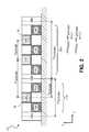
- FIG. 2is a cross-sectional view of a microelectronic device 200 including three adjacent non-planar transistors with through gate fin isolation in accordance with an embodiment of the present invention.
- FIG. 2illustrates semiconductor fins 210 A and 290 A in a cross-sectional view akin to that of FIG. 1B .
- FIG. 2may be considered an extended view of FIG. 1 that further illustrates devices adjacent to the inverter 202 .
- the gate electrode 220is disposed over the semiconductor fin 210 A while two gate electrodes 220 B and 220 C are disposed over the semiconductor fin 290 A.
- the isolation region 150 Bseparates the fin 210 A from the fin 290 A.
- centerlines of the gate electrodes 220 B and 220 Cdefine the minimum gate electrode pitch, P Gate,Min .
- P Gate,Minthe minimum gate electrode pitch
- centerlines of gate electrodes 220 and 220 B, separated by the intervening isolation region 150 Bare at an integer multiple of the minimum gate electrode pitch (e.g., twice P Gate,Min ).
- centerlines of the gate electrodesremain at an integer multiple of the minimum gate electrode pitch.
- adjacent isolation regions separated by one or more intervening gate electrodeare at an integer multiple of the minimum gate electrode pitch.
- isolation regions 150 A and 150 B surrounding fin 210 Aare at twice P Gate,Min and isolation regions 150 B and 150 N surrounding fin 290 A are at three times P Gate,Min .
- all isolation regions 150 A, 150 B, 150 N and gate electrodes 220 , 220 B, 220 Care at the same (substantially equal, fixed) pitch with adjacent isolation regions and electrodes at a minimum pitch.
- FIGS. 1A , 1 B and FIG. 2illustrate the same characteristic with the isolation stripe pitch P 4 being substantially equal to the gate electrode stripe pitch P 3 .
- the isolation regions 150 A, B, Care interdigitated with the gate electrodes 120 , 220 with both being at integer multiples of a fixed minimum stripe pitch (e.g., P 1 ).
- a plurality of isolation stripesare self-aligned to a plurality of gate electrode stripes disposed over a plurality of semiconductor fins with the plurality of isolation regions having no misregistration with the plurality of gate electrodes.
- FIGS. 3A , 3 B and 3 Care cross-sectional views of through gate isolation with various alternative substrate and transistor architectures, in accordance with embodiments.
- the FIGS. 3A-3Care illustrations along a cross-section plane analogous to that denoted by the A-A′ line in FIG. 1A .
- the non-planar transistor 301includes a semiconductor fin 310 disposed on an SOI substrate 105 that includes both an isolation dielectric layer 106 and a handling substrate 107 .
- the through gate isolation regions 150have the same structural relationship with the gate electrode 120 (and gate stack including the gate electrode 120 and gate dielectric layer 165 ) as was described in the context of FIGS. 1A , 1 B and FIG. 2 with the additional clarification that the isolation regions 150 extend all the way through the semiconductor fin 310 and make direct contact with the isolation dielectric layer 107 .
- FIG. 3Bfurther illustrates a bulk substrate embodiment where the non-planar transistor 302 includes a semiconductor fin 310 having crystallographic continuity with the semiconductor substrate 105 (the dashed line denoting where a top surface of the substrate 105 is out of the plane of the FIG. 3B ).
- the isolation regions 150extend down through the semiconductor fin 310 preferably at least to the top surface of substrate 105 and more preferably to a level into the substrate 105 that is below the top substrate surface for reduced leakage, latch-up, etc.
- FIG. 3Cfurther illustrates an embodiment with a nanowire transistor 303 where at least one semiconductor nanowire 310 A is surrounded on all sides by the gate electrode 120 (and gate dielectric layer 165 ).
- the semiconductor nanowire 310 Amay be of any semiconductor composition described elsewhere herein in the general context of a semiconductor fin. Additional nanowires (e.g., 310 B) may form a vertical (z-dimension) stack of nanowires, in which case the isolation regions 150 pass through the z-thicknesses of every nanowire, and may further extend down to the substrate 105 .
- FIGS. 3A , 3 B and 3 Cembodiments of the present invention are not limited with respect to either the substrate 105 or the semiconductor fin geometry.
- isolationbifurcates a semiconductor fin at one or more isolation points that is self-aligned to the gate electrode. These self-aligned isolation points then become the isolation regions between adjacent fins.
- self-alignment of the isolation points between adjacent finsis achieved by defining a set of sacrificial precursor, or “placeholder” features having dimensions which ultimately dictate those of both the gate electrodes and the isolation regions. Once these placeholder features are defined, subsets of the placeholder features are then modified separately and independently to complete formation of isolation regions and the gate electrodes. As the sacrificial placeholder features are formed concurrently, for example with a single masking level, isolation regions and gate electrodes may be perfectly aligned at a given minimum feature pitch.
- FIG. 4is a flow diagram describing a through gate fin isolation fabrication method 401 , in accordance with certain embodiments.
- FIGS. 5A , 5 B, 5 C, 5 D, 5 E, 5 F, 5 G, and 5 Hare plan views illustrating an evolution of non-planar transistor and through gate fin isolation structures as the through gate fin isolation fabrication method 401 is performed, in accordance with one exemplary embodiment.
- FIGS. 6A , 6 B, 6 C, 6 D, 6 E, 6 F, 6 G and 6 Hare cross-sectional views along the A-A′ line denoted in the corresponding FIG. 5A-5H .
- FIG. 5Ashows a plan view of a semiconductor fin 510 formed on substrate 505 .
- a cross-sectional view along the A-A′ line extending longitudinally along the fin 510is further illustrated in FIG. 6A .
- the semiconductor fin 510is of a first length, which is not limiting with respect to embodiments of the present invention beyond being sufficiently long to ultimately form at least one non-planar transistor, preferably at least two non-planar transistors, and ideally a very great many transistors.
- Any technique known in the artmay be utilized to form the semiconductor fin 510 at operation 405 , such as, but not limited to plasma etching and/or wet chemical etching.
- placeholdersare formed.
- placeholder stripes 518 A, 518 B, 518 C and 518 Dare formed orthogonally over the semiconductor fin 510 .
- the placeholder stripes 518 A, 518 B, 518 C, and 518 Dare substantially parallel to each other and may be printed with a mask that advantageously leverages optical properties of such a periodic structure (i.e., grating) to achieve a minimum pitch between the placeholder stripes.
- the placeholder stripes 518 A- 518 Dare planarized regions formed in a surrounding material 544 .
- a variety of materialsmay be utilized for the placeholder stripes 518 A- 518 D, such as but not limited to, polysilicon, germanium, and SiGe, while the surrounding material 544 is of a composition at least offering a basis for subsequent etch selectivity, and preferably is a dielectric, such as, but not limited to, one or more of silicon dioxide, silicon nitride, or low-k dielectrics having a dielectric constant below that of silicon dioxide, such as, but not limited to carbon-doped oxide (CDO).
- CDOcarbon-doped oxide
- source/drain regionsare formed. Although, in general, source/drain region may be performed at various points in the method 401 , in the exemplary embodiment, the source/drain regions are formed prior to removing any of the placeholders formed at operation 410 . As illustrated in FIGS. 5C and 6C , source/drain regions 530 are formed between the placeholder stripes 518 A- 518 D. In the exemplary embodiment, along the centerline of the fin 510 , the source/drain regions 530 occupy the entire z-height of the fin down to the substrate 505 .
- source/drain regionsmay have a z-height different than that of a fin (e.g., greater or lesser z-height than that of a fin).
- any source/drain formation process applicable to a non-planar devicemay be employed at operation 415 , beginning with removal of the surrounding material 544 (selectively to the placeholder strips 518 A- 518 D).
- a dopant speciese.g., boron, arsenic, phosphorous, etc.
- an epitaxial layeris deposited on the fin 510 to form the source/drain regions 530 .
- Any epitaxial material composition known in the artmay be utilized, such as, but not limited, to doped Si, doped Ge, doped SiGe, and doped SiC.
- the source/drain regions 530may have a z-height elevated, or raised, beyond that of the fin 510 , as is illustrated in FIG. 6C . As further illustrated in FIG.
- the maximum transverse width of the fin 510 within the source/drain regions 530may also increase relative to the channel portion of the fin 510 .
- portions of the fin 510 exposed by removal of the surrounding material 544are removed (etched) and semiconductor then regrown, for example with an epitaxial deposition process, to form an embedded epitaxial source/drain, which may also be raised, but need not be necessarily.
- the placeholder stripes 518 A- 518 Dmay be re-planarized, for example with deposition of another surrounding material 545 , such as a flowable dielectric, and a polish, if desired.
- the method 401proceeds with removing a subset of the placeholders at operation 420 (selective to the surrounding material 545 ).
- the selective removal of a subset of the placeholdersmay be performed with a patterned etch, for example as illustrated in FIGS. 5D and 6D .
- the masking features 578may be any conventional masking material, such as, but not limited to, a photoresist, or a non-photosensitive hardmask, such as amorphous (CVD) carbon, or spin-on organics.
- overlayneed only be sufficient to ensure first placeholders 518 A and 518 C are protected while second placeholders 518 B and 518 D are exposed.
- operation 420is completed with removal of the exposed placeholders 518 B, 518 D, to form openings 560 B and 560 D exposing portions 575 A and 575 B of the semiconductor fin 510 .
- Removal of the exposed placeholders 518 B, 518 Dmay be with any etch process (e.g., plasma and/or wet chemical) that has adequate selectivity to the placeholder material (e.g., polysilicon) over the surrounding material 545 (e.g., silica, CDO, etc.) so that the openings 560 B and 560 D are self-aligned to the placeholders 518 B, 518 D.
- etch processe.g., plasma and/or wet chemical
- the placeholder materiale.g., polysilicon
- surrounding material 545e.g., silica, CDO, etc.
- semiconductor fin portions exposed by removal of some of the placeholder featuresare then removed to bifurcate the semiconductor fin at isolation points.
- the first semiconductor fin portions 575 A and 575 Bare etched away, for example down to the substrate 505 , which bifurcates or “cuts” the semiconductor fin 510 into separate semiconductor fins 510 A and 510 B.
- One or more plasma and/or wet chemical etchesmay be performed, as dependent on the composition of the semiconductor fin, with the openings 560 B and 560 D controlling the dimensioning of the cut through the semiconductor fin.
- An etch process similar to that employed to initially form the semiconductor fin 510 (at operation 405 )may be utilized, for example.
- the openings 560 B and 560 Dare self-aligned to the placeholders that were removed (e.g., 518 B, 518 D) and therefore also self-aligned to the remaining placeholders (e.g., 518 A and 518 C). It should be noted that while the openings 560 B and 560 D are self-aligned, in particular embodiments, the width (x-dimension) of such openings may vary somewhat as a function of etch bias in the fin etch.
- An advantageous etch biasmay shrink the opening widths to further increase transistor density, or an etch bias may increase the opening width to further increase transistor isolation, or an etch bias may exactly maintain the opening.
- centerlines of the openings 560 B and 560 Dremain self-aligned to centerlines of the remaining placeholders 518 A and 518 C.
- a dielectric materialis filled into the openings where the fin portions were removed to complete formation of the isolation regions 550 , as is further illustrated in FIGS. 5G and 6G .
- any dielectric fillmay be utilized, such as, but not limited to high density plasma (HDP) and flowable dielectric processes.
- a dielectric material which induces a stress on the fins 510 A and 510 Bmay be deposited into the openings 560 B, 560 D.
- one or more remaining placeholdersare then removed at operation 450 ( FIG. 4 ).
- the placeholders 518 A and 518 Chave been removed, again selectively to the surrounding material 545 and selectively to isolation region 550 .
- Openings 560 A and 560 C ( FIG. 5G ) exposing second semiconductor fin regions 585 A and 585 Bare therefore again self-aligned to the sacrificial placeholder features, and as such, self-aligned to the isolation regions 550 .
- the method 401then completes with forming gate stacks at operation 460 using any formation technique known in the art, such as, but not limited to chemical vapor deposition (CVD), atomic layer deposition (ALD), and physical vapor deposition (PVD).
- CVDchemical vapor deposition
- ALDatomic layer deposition
- PVDphysical vapor deposition
- the gate dielectric 565 and gate electrodes 520 A and 520 B having any suitable work functionmay be deposited into the openings 560 A and 560 C, as dimensioned by the placeholder formation operation 410 to be self-aligned to the placeholder features and, as such, self-aligned to the isolation regions 550 .
- the through gate isolation technique demonstrated by the method 401has been found to have the further advantage of maintaining a significant portion of the fin stress.
- this advantageis currently thought to stem from bifurcating the fins after the placeholder features are formed, and more particularly after both the placeholder features and source/drain regions are formed.
- the presence of the placeholder features and dielectric covering source-drain regionsserve as reinforcement, mechanically holding the semiconductor fin while the isolation cuts are made and thereby locking-in a large portion of the channel strain.
- the isolation regions 150then perform a similar strain-retention function while the remaining placeholder features are removed and replaced with non-sacrificial gate stacks.
- the stress remaining after cutting the finis at least 50% of the stress present at initial fin formation (e.g., at operation 430 ) for both tri-gate and nanowire embodiments.
- removing a same portion of the fin prior to forming the placeholder structureswas found to retain only about 15-20% of the initial channel stress.
- FIG. 7is a functional block diagram of a mobile computing platform 700 which employs an IC including circuitry using non-planar transistors with through gate isolation in accordance with embodiments of the present invention (e.g., inverter 100 illustrated in FIG. 1A is present in the platform 700 ).
- the mobile computing platform 700may be any portable device configured for each of electronic data display, electronic data processing, and wireless electronic data transmission.
- mobile computing platform 700may be any of a tablet, a smart phone, laptop computer, etc. and includes a display screen 705 which in the exemplary embodiment is a touchscreen (capacitive, inductive, resistive, etc.), a chip-level (SoC) or package-level integrated system 710 , and a battery 713 .
- a display screen 705which in the exemplary embodiment is a touchscreen (capacitive, inductive, resistive, etc.), a chip-level (SoC) or package-level integrated system 710 , and a battery 713 .
- SoCchip-level
- the greater the carrier mobility of each transistor in the system 710the greater the functionality.
- the through gate isolation architecture and techniques described hereinenable performance and form factor improvements in the mobile computing platform 700 .
- packaged device 777includes at least one memory chip (e.g., RAM), or at least one processor chip (e.g., a multi-core microprocessor and/or graphics processor) including through gate isolation.
- the packaged device 777is further coupled to the board 260 along with, one or more of a power management integrated circuit (PMIC) 715 , RF (wireless) integrated circuit (RFIC) 725 including a wideband RF (wireless) transmitter and/or receiver (e.g., including a digital baseband and an analog front end module further comprises a power amplifier on a transmit path and a low noise amplifier on a receive path), and a controller thereof 711 .
- PMICpower management integrated circuit
- RFICwireless integrated circuit
- the PMIC 715performs battery power regulation, DC-to-DC conversion, etc., and so has an input coupled to the battery 713 and with an output providing a current supply to all the other functional modules.
- the RFIC 725has an output coupled to an antenna to provide to implement any of a number of wireless standards or protocols, including but not limited to Wi-Fi (IEEE 802.11 family), WiMAX (IEEE 802.16 family), IEEE 802.20, long term evolution (LTE), Ev-DO, HSPA+, HSDPA+, HSUPA+, EDGE, GSM, GPRS, CDMA, TDMA, DECT, Bluetooth, derivatives thereof, as well as any other wireless protocols that are designated as 3G, 4G, 5G, and beyond.
- each of these board-level modulesmay be integrated onto separate ICs coupled to the package substrate of the packaged device 777 or within a single IC (SoC) coupled to the package substrate of the packaged device 777 .
- FIG. 8is a functional block diagram of a computing device 1000 in accordance with one embodiment of the invention.
- the computing device 1000may be found inside the platform 700 , for example, and further includes a board 1002 hosting a number of components, such as but not limited to a processor 1004 (e.g., an applications processor) and at least one communication chip 1006 .
- a processor 1004e.g., an applications processor
- at least one of the processor 1004 and communication chip 1006incorporate non-planar transistors with through gate isolation, as described elsewhere herein.
- the processor 1004is physically and electrically coupled to the board 1002 .
- the processor 1004includes an integrated circuit die packaged within the processor 1004 .
- the term “processor”may refer to any device or portion of a device that processes electronic data from registers and/or memory to transform that electronic data into other electronic data that may be stored in registers and/or memory.
- the at least one communication chip 1006is also physically and electrically coupled to the board 1002 .
- the communication chip 1006is part of the processor 1004 .
- computing device 1000may include other components that may or may not be physically and electrically coupled to the board 1002 .
- volatile memorye.g., DRAM
- non-volatile memorye.g., ROM
- flash memorye.g., a graphics processor, a digital signal processor, a crypto processor, a chipset, an antenna, touchscreen display, touchscreen controller, battery, audio codec, video codec, power amplifier, global positioning system (GPS) device, compass, accelerometer, gyroscope, speaker, camera, and mass storage device (such as hard disk drive, solid state drive (SSD), compact disk (CD), digital versatile disk (DVD), and so forth).
- volatile memorye.g., DRAM
- non-volatile memorye.g., ROM
- flash memorye.g., a graphics processor, a digital signal processor, a crypto processor, a chipset, an antenna, touchscreen display, touchscreen controller, battery, audio codec, video codec, power amplifier, global positioning system (GPS) device, compass, accelerometer, gyroscope, speaker, camera, and mass storage device
- At least one of the communication chips 1006enables wireless communications for the transfer of data to and from the computing device 1000 .
- the term “wireless” and its derivativesmay be used to describe circuits, devices, systems, methods, techniques, communications channels, etc., that may communicate data through the use of modulated electromagnetic radiation through a non-solid medium. The term does not imply that the associated devices do not contain any wires, although in some embodiments they might not.
- the communication chip 1006may implement any of a number of wireless standards or protocols, including but not limited to those described elsewhere herein.
- the computing device 1000may include a plurality of communication chips 1006 .
- a first communication chip 1006may be dedicated to shorter range wireless communications such as Wi-Fi and Bluetooth and a second communication chip 1006 may be dedicated to longer range wireless communications such as GPS, EDGE, GPRS, CDMA, WiMAX, LTE, Ev-DO, and others.
- One embodimentis a microelectronic device, including a first gate electrode disposed over a first semiconductor fin, a second gate electrode disposed over a second semiconductor fin, a first isolation region disposed between the first and second gate electrodes and separating adjacent ends of the first and second semiconductor fins with the first electrode, second gate electrode, and first isolation region being substantially parallel with longitudinal centerlines at a substantially equal pitch.
- the microelectronic devicefurther includes a second isolation region disposed on an end of the first semiconductor fin opposite the first isolation region with centerlines of the first and second isolation regions defining an isolation region pitch that is an integer multiple of a minimum pitch for the gate electrodes.
- centerlines the first and second gate electrodesdefine a gate electrode pitch that is an integer multiple of the minimum gate electrode pitch.
- the gate electrode pitchis substantially equal to the isolation region pitch with the gate electrodes and isolation regions forming stripes at a minimum stripe pitch.
- the microelectronic devicefurther includes a third gate electrode disposed over the first semiconductor fin between the first and second isolation regions with centerlines of the first and third gate electrodes at the minimum stripe pitch and the isolation region pitch being substantially equal to at least two times the minimum stripe pitch.
- the isolation regionabuts the ends of the first and second semiconductor fins and has a transverse width that is no larger than a width of a gate stack that includes both the gate electrode and a gate dielectric layer in contact with the gate electrode.
- the microelectronic devicefurther comprises a third and fourth semiconductor fins with the first gate electrode disposed over both the first and third semiconductor fins and the second gate electrode disposed over both the second and fourth semiconductor fins, and with the first isolation region separating adjacent ends of the first and second semiconductor fins as well as ends of the third and fourth semiconductor fins.
- the first semiconductor finincludes source and drain regions of a conductivity type complementary to source and drain regions in the third semiconductor fin
- the second semiconductor finincludes source and drain regions of a conductivity type complementary to source and drain regions of the fourth semiconductor.
- One embodimentis a microelectronic device including a plurality of gate electrode stripes disposed over a plurality of semiconductor fins, and a plurality of isolation stripes substantially parallel to the plurality of gate electrode stripes and disposed between adjacent ones of the plurality of semiconductor fins.
- the plurality of isolation stripesare self-aligned to the plurality of gate electrode stripes.
- the plurality of gate electrode stripes and plurality of isolation stripeshave a pitch that is an integer multiple of a minimum stripe pitch.
- the plurality of gate electrode stripesare interdigitated with the plurality of isolation stripes to have one or more gate electrode stripe between adjacent isolation stripes and/or to have one or more isolation stripes between adjacent gate electrode stripes to form a population of stripes of a fixed pitch.
- a method of fabricating a microelectronic deviceincludes receiving a semiconductor fin disposed over a substrate, forming a gate electrode over the semiconductor fin, and bifurcating the semiconductor fin at an isolation point that is self-aligned to the gate electrode.
- bifurcating the semiconductor fin at the isolation pointfurther includes defining dimensions of the gate electrode and dimensions of the isolation point with a single lithographic patterning mask.
- bifurcating the semiconductor fin at the isolation pointfurther includes removing a first portion of the semiconductor fin at the isolation point selectively to a second portion of the semiconductor fin over which the gate electrode is disposed.
- defining dimensions of the gate electrode and dimensions of the isolation point with a single lithographic patterning maskfurther includes defining a plurality of gate electrode placeholders over the semiconductor fin.
- the fabrication embodimentsmay further include removing a subset of the gate electrode placeholders to expose the first portion of the fin.
- a microelectronic deviceis fabricated by forming a plurality of sacrificial placeholders over a semiconductor fin, removing a subset of the sacrificial placeholders, removing a portion of the fin exposed by the placeholder removal, depositing a dielectric material where fin portion was removed, and replacing a second subset of the sacrificial placeholders a non-sacrificial gate stack.
- forming the plurality of sacrificial placeholdersfurther comprises forming three placeholders over two semiconductor fins, removing the first subset of the sacrificial placeholders comprises removing a center one of the three sacrificial placeholders, removing a portion of the semiconductor fin exposed by the placeholder removal further comprises bifurcating the semiconductor fin into first and second semiconductor fins, and replacing the second subset of sacrificial placeholders comprises removing a remaining two of the three sacrificial placeholders to form openings exposing second portions of the first and second semiconductor fins, and forming a first and second gate stack over the second portions of the first and second semiconductor fins.
- removing a center one of the three sacrificial placeholderscomprises masking off an outer pair of the three sacrificial placeholders.
- forming the plurality of sacrificial placeholders over the semiconductor finfurther comprises printing a grating pattern of a fixed pitch.
- the lattice mismatchinduces a first level of stress in the fins and the sacrificial placeholder maintains at least 50% of the first level of stress in the fins after removing the portion of the fin.
- the plurality of semiconductor finscomprises a SiGe alloy while the substrate is a silicon substrate.
Landscapes
- Insulated Gate Type Field-Effect Transistor (AREA)
- Metal-Oxide And Bipolar Metal-Oxide Semiconductor Integrated Circuits (AREA)
- Semiconductor Memories (AREA)
Abstract
Description
- Embodiments of the invention generally relate to transistor architectures and fabrication, and more particularly relate to electrical isolation of adjacent non-planar (fin) transistors formed on a substrate.
- The microelectronics industry is now in transition from a planar to a non-planar field effect transistor (i.e., Tri-gate or FinFET) continuing with device scaling as charted by Moore's Law. Pioneers of non-planar transistor technology are now developing second generation non-planar devices and achieving ever higher levels of transistor performance and density. In addition to scaling of individual transistors, the number of transistors of a given channel length that can be fabricated within a given substrate area (i.e., transistor density) is also very important to achieve higher transistor counts for greater levels of integrated circuit (IC) functionality.
- Non-planar transistors which utilize a fin of semiconductor material protruding from a substrate surface employ a gate electrode that wraps around two, three, or even all sides of the fin (i.e., dual-gate, tri-gate, nanowire transistors). Source and drain regions are then formed in the fin, or as re-grown portions of the fin, on either side of the gate electrode. To isolate a source/drain region of a first non-planar transistor from a source/drain region of an adjacent second non-planar transistor, a gap or space may be formed between two adjacent fins. Such an isolation gap generally requires a masked etch of some sort. Once isolated, a gate stack is then patterned over the individual fins, again typically with a masked etch of some sort (e.g., a line etch or an opening etch depending on the specific implementation).
- Embodiments of the present invention are illustrated by way of example, and not by way of limitation, and can be more fully understood with reference to the following detailed description when considered in connection with the figures in which:
FIG. 1A is a plan view of two adjacent inverters (or NOT gates) employing non-planar transistors and through gate fin isolation in accordance with an embodiment of the present invention;FIG. 1B is a cross-sectional view of two adjacent non-planar transistors fromFIG. 1A , further illustrating the through gate fin isolation, in accordance with an embodiment;FIG. 2 is a cross-sectional view of three adjacent non-planar transistors with through gate fin isolation in accordance with an embodiment of the present invention;FIGS. 3A ,3B and3C are cross-sectional views of through gate isolation applied to various substrate and transistor architectures, in accordance with embodiments;FIG. 4 is a flow diagram describing a through gate fin isolation fabrication process, in accordance with embodiments;FIGS. 5A ,5B,5C,5D,5E,5F,5G and5H are plan views illustrating an evolution of non-planar transistor and through gate fin isolation structures as a through gate fin isolation fabrication process is performed, in accordance with an embodiment;FIGS. 6A ,6B,6C,6D,6E,6F,6G and6H are cross-sectional views corresponding toFIGS. 5A ,5B,5C,5D,5E,5F,5G and5H further illustrating an evolution of non-planar transistor and through gate fin isolation structures as a through gate fin isolation fabrication process is performed, in accordance with an embodiment;FIG. 7 is an isometric view of a mobile computing platform employing an IC having non-planar transistor and through gate fin isolation structures, in accordance with an embodiment of the present invention; andFIG. 8 is a functional block diagram of the mobile device illustrated inFIG. 7 , in accordance with an embodiment of the present invention.- In the following description, numerous details are set forth, however, it will be apparent to one skilled in the art, that the present invention may be practiced without these specific details. In some instances, well-known methods and devices are shown in block diagram form, rather than in detail, to avoid obscuring the present invention. Reference throughout this specification to “an embodiment” means that a particular feature, structure, function, or characteristic described in connection with the embodiment is included in at least one embodiment of the invention. Thus, the appearances of the phrase “in an embodiment” in various places throughout this specification are not necessarily referring to the same embodiment of the invention. Furthermore, the particular features, structures, functions, or characteristics may be combined in any suitable manner in one or more embodiments. For example, a first embodiment may be combined with a second embodiment anywhere the two embodiments are not specified to be mutually exclusive.
- The terms “coupled” and “connected,” along with their derivatives, may be used herein to describe structural relationships between components. It should be understood that these terms are not intended as synonyms for each other. Rather, in particular embodiments, “connected” may be used to indicate that two or more elements are in direct physical or electrical contact with each other. “Coupled” my be used to indicated that two or more elements are in either direct or indirect (with other intervening elements between them) physical or electrical contact with each other, and/or that the two or more elements co-operate or interact with each other (e.g., as in a cause an effect relationship).
- The terms “over,” “under,” “between,” and “on” as used herein refer to a relative position of one material layer or component with respect to other layers or components. For example, one layer disposed over or under another layer may be directly in contact with the other layer or may have one or more intervening layers. Moreover, one layer disposed between two layers may be directly in contact with the two layers or may have one or more intervening layers. In contrast, a first layer “on” a second layer is in direct contact with that second layer. Similarly, unless explicitly stated otherwise, one feature disposed between two features may be in direct contact with the adjacent features or may have one or more intervening features.
- One problem with the fin isolation techniques described in the background is that the gates are not self-aligned with the ends of the fins, and alignment of the gate stack pattern with the semiconductor fin pattern relies on overlay of these two patterns. As such, lithographic overlay tolerances are added into the dimensioning of the semiconductor fin and the isolation gap with fins needing to be of greater length and isolation gaps larger than they would be otherwise for a given level of transistor functionality. Device architectures and fabrication techniques that reduce such over-dimensioning therefore offer highly advantageous improvements in transistor density.
- Another problem with the fin isolation techniques described in the background is that stress in the semiconductor fin desirable for improving carrier mobility may be lost from the channel region of the transistor where too many fin surfaces are left free during fabrication, allowing fin strain to relax. Device architectures and fabrication techniques that maintain higher levels of desirable fin stress therefore offer advantageous improvements in non-planar transistor performance.
- Through gate fin isolation architectures and techniques are described herein. In the exemplary embodiments illustrated, non-planar transistors in a microelectronic device, such as an integrated circuit (IC) are isolated from one another in a manner that is self-aligned to gate electrodes of the transistors. Although embodiments of the present invention are applicable to virtually any IC employing non-planar transistors, exemplary ICs include, but are not limited to, microprocessor cores including logic and memory (SRAM) portions, RFICs (e.g., wireless ICs including digital baseband and analog front end modules), and power ICs.
- In embodiments, two ends of adjacent semiconductor fins are electrically isolated from each other with an isolation region that is positioned relative to gate electrodes with the use of only one patterning mask level. In an embodiment, a single mask is employed to form a plurality of sacrificial placeholder stripes of a fixed pitch, a first subset of the placeholder stripes define a location and/or dimension of isolation regions while a second subset of the placeholder stripes defines a location and/or dimension of a gate electrode. In certain embodiments, the first subset of placeholder stripes is removed and isolation cuts made into the semiconductor fins in the openings resulting from the first subset removal while the second subset of the placeholder stripes is ultimately replaced with non-sacrificial gate electrode stacks. Because a subset of placeholders utilized for gate electrode replacement are employed to form the isolation regions, the method and resulting architecture is referred to herein as “through gate” isolation. One or more through-gate isolation embodiment described herein may, for example, enable higher transistor densities and higher levels of advantageous transistor channel stress.
- With isolation defined after placement/definition of the gate electrode, a greater transistor density can be achieved because fin isolation dimensioning and placement can be made perfectly on-pitch with the gate electrodes so that both gate electrodes and isolation regions are integer multiples of a minimum feature pitch of a single masking level. In further embodiments where the semiconductor fin has a lattice mismatch with a substrate on which the fin is disposed, greater degrees of strain are maintained by defining the isolation after placement/definition of the gate electrode. For such embodiments, other features of the transistor (such as the gate electrode and added source and/or drain materials) that are formed before ends of the fin are defined help to mechanically maintain fin strain after an isolation cut is made into the fin.
FIG. 1A is a plan view of amicroelectronic device 100 including two adjacent CMOS inverters (or NOT gates)101 and202 employing non-planar transistors and through gate fin isolation in accordance with an embodiment of the present invention.FIG. 1B is a cross-sectional view along the A-A′ line passing through two adjacent semiconductor fins fromFIG. 1A , further illustrating through gate fin isolation, in accordance with an embodiment. While the exemplary embodiment is illustrated in the context of particular logic gates for clarity of description, it is to be appreciated that any integrated circuit elements may be implemented with through gate fin isolation in a similar manner to benefit from the same technical advantages illustrated in the context of themicroelectronic device 100.- As shown in
FIGS. 1A and 1B , agate electrode 120 is disposed over asemiconductor fin 110A. Thesemiconductor fin 110A protrudes from a surface of thesubstrate 105 so that thegate electrode 120 wraps around two (e.g., opposing fin sidewalls out of the plane ofFIG. 1B ) or three sides (e.g., top surface of the fin as shown inFIG. 1B and opposing fin sidewalls for a tri-gate embodiment). Beyond thefin 110A having sidewalls which are electrically (capacitively) coupled to thegate electrode 120, thefin 110A may have any number of shapes. Generally, thesubstrate 105 may be any known in the art suitable for the purpose of fabricating non-planar transistors, including, but not limited to, bulk substrates which may be any conventional material, such as, but not limited to single crystalline silicon, germanium, III-V compound semiconductor (e.g., GaAs, InP, etc.), III-Nitride compound semiconductor (e.g., GaN), or sapphire. In alternate embodiments, as further illustrated elsewhere herein, semiconductor on insulator (SOI) substrates are utilized. - The
semiconductor fin 110A may also be of any semiconducting material composition known in the art to be suitable for the purpose of fabricating non-planar transistors, including, but not limited to, single crystalline silicon (e.g., either having continuity with thesubstrate 105 for bulk embodiments or separated from thesubstrate 105 by an intervening material for SOI embodiments). As further described elsewhere herein, in certain advantageous embodiments thesemiconductor fin 110A is of a semiconductor material that has a different lattice constant than that of the substrate105 (i.e., lattice mismatched). Examples include, but are not limited to SiGe alloys. For such embodiments, thesemiconductor fin 110A may be either lattice strained for high carrier mobility (e.g., as for a 25-35% Ge SiGe alloy) or lattice relaxed (e.g., as for a III-V or III-N semiconductor fin) with some of the benefits of through gate isolation embodiments implemented with lattice strained semiconductor fins discussed more specifically elsewhere herein. - The
gate electrode 120, as illustrated inFIG. 3A , is a portion of a gate electrode stack which further includes agate dielectric layer 165 illustrated inFIG. 1B . Generally, thegate electrode 120 andgate dielectric layer 165 may be of any material compositions known in the art to be applicable to non-planar transistors with many known ultra high-k materials (e.g., having a dielectric constant above that of Si3N4) ,as well as silicon nitride and silicon dioxide, being viable options for the embodiments described herein. - The
semiconductor fin 110A further includes a first source/drain region 130A and a second source/drain region 130B disposed on either side of thegate electrode 120. The source/drain regions 120A,130A may be doped regions of thesemiconductor fin 110A and may include regrown or epitaxially deposited semiconductor regions. Generally, each of theCMOS inverter 101 andCMOS inverter 202 includes a transistor of a first conductivity type (e.g., N-type) and a transistor of a second, complementary, conductivity type (e.g., P-type). As such, themicroelectronic device 100 includes a pair of transistors of each complementary type. While these complementary transistor pairings may be implemented in a number of manners within the confines of the present invention, in the exemplary embodiment, a first transistor employing thesemiconductor fin 110A has source/drain regions semiconductor fin 210A has source/drain regions semiconductor fin 115A has source/drain regions semiconductor fin 215A has source/drain regions drain contacts - Notably, a microelectronic device may include any number of non-planar transistors electrically coupled together in parallel for a greater current carrying channel width and embodiments of the present invention are not limited in this respect. For the exemplary
microelectronic device 100, each of thesemiconductor fins fins drain regions drain contacts - As illustrated in
FIG. 1A , in embodiments, the longitudinal length of thegate electrode 120 is significantly greater (e.g., more than twice) than a transverse width of thegate electrode 120 and is therefore referred to herein as a gate electrode “stripe.” InFIG. 1A ,first gate electrode 120 has a longitudinal length sufficient to extend over both thesemiconductor fins inverter 101. Thegate electrode 220 is similarly dimensioned as a gate electrode stripe. While the description herein should make the advantages of such architecture apparent to one of ordinary skill, it is noted that this particular feature is not required by embodiments of the present invention. - In an embodiment, a first isolation region is disposed between first and second gate electrodes and separates adjacent ends of first and second semiconductor fins. As shown in
FIG. 1A , anisolation region 150A is disposed between thegate electrodes first semiconductor fin 110A and thesecond semiconductor fin 210A. In the exemplary embodiment, theisolation region 150A is dimensioned, like thegate electrodes FIG. 1A , theisolation region 150A has a longitudinal length sufficient to also extend between thesemiconductor fins invertors 101 and102 employ paralleled pluralities of fins for greater current carrying channel width, theisolation region 150A separates one paralleled plurality of fins (e.g.,fins inverter 101 from a second paralleled plurality of fins (e.g.,fins inverter 202. - In embodiments of the present invention, the isolation region disposed between adjacent semiconductor fins is self-aligned to a gate electrode. As shown in
FIG. 1A , the edges of thefirst isolation region 150A are aligned with the end faces of both thesemiconductor fins isolation region 150A abuts both the adjacent ends of thesemiconductor fins FIGS. 1A and 1B , a longitudinal centerline thefirst isolation region 150A (denoted by a dashed line) is disposed equidistant from, and parallel to, longitudinal centerlines of thegate electrodes first gate electrode 120 and theisolation region 150A, and P2representing a second pitch between centerlines of theisolation region 150A and thesecond gate electrode 220, P1is substantially equal to P2so that theisolation region 150A is “on-pitch” with the gate electrode pitch P3defined by centerlines of thegate electrodes isolation region 150A andgate electrodes isolation region 150A andgate electrodes first isolation region 150A to thegate electrodes 120,220A. The term “substantially” in the context of the phrase “equal pitch” acknowledges that all manufacturing processes have tolerances and therefore the resulting structures are never truly perfect. For example, even in an embodiment where a single mask is employed to form isolation regions self-aligned with gate electrodes, the single mask can still be expected to have some tolerance across three mask features spaced apart at a same, equal design rule. As such, tolerances much smaller than those of overlay between two masks are achieved by certain embodiments described herein, such that P1and P2are “substantially equal,” with P1being within 10% of P2in first embodiments, P1being within 5% of P2in second embodiments, P1being within 3% of P2in third embodiments, and P1being within 1% of P2in fourth embodiments - In embodiments, the isolation region has a dimension that is substantially equal to a width of a gate stack. Here again, the term “substantially” is employed because there are tolerances inherent to a given fabrication process with the substantial equality being within 10% in first embodiments, within 5% in second embodiments, within 3% in third embodiments, and within 1% in fourth embodiments. As shown in
FIG. 1B , the gate stack includes both thegate electrode 120 and agate dielectric layer 165 in contact with thegate electrode 120. Depending on the implementation, the width of a gate stack may differ from the width of a gate electrode where gate dielectric is present on more than a bottom surface of the gate electrode. In the embodiment ofFIG. 1B , thegate electrode 120 is disposed within a well having thegate dielectric layer 165 present on the well sidewalls such that the transverse width of the gate stack L1is approximately twice the thickness of thegate dielectric layer 165 added to the transverse width of the gate electrode120 (and associated with a transistor channel length). Of course, in other embodiments where the gate dielectric is only present at the interface of a gate electrode and a semiconductor fin, the width of the gate stack is substantially equal to the width of the gate electrode. As further shown inFIG. 1B , the transverse width of theisolation region 150A is L2with L2being approximately equal to L1(e.g., within 10%), and preferably no larger than L1. Along with the self-alignment of theisolation region 150A, minimal transverse dimensioning of theisolation region 150A advantageously reduces the x-dimension of thesubstrate 105 occupied by theinverters 101 and202 (i.e., reduces area of an inverter unit cell). - In embodiments, a second isolation region is disposed on an end of a semiconductor fin opposite the first isolation region. As shown in
FIGS. 1A and 1B , for example, anisolation region 150B is disposed on an end of thesemiconductor fin 210A opposite thefirst isolation region 150A. Centerlines of theisolation region 150A and theisolation region 150B define an isolation pitch P4. In embodiments, the isolation pitch is an integer multiple of a minimum pitch for the gate electrodes (PGate,min). FIG. 2 is a cross-sectional view of amicroelectronic device 200 including three adjacent non-planar transistors with through gate fin isolation in accordance with an embodiment of the present invention.FIG. 2 , illustratessemiconductor fins FIG. 1B . For example,FIG. 2 may be considered an extended view ofFIG. 1 that further illustrates devices adjacent to theinverter 202. Thegate electrode 220 is disposed over thesemiconductor fin 210A while twogate electrodes semiconductor fin 290A. Theisolation region 150B separates thefin 210A from thefin 290A. Because there is no isolation region between thegate electrodes gate electrodes isolation region 150B being on-pitch with the gate electrode pitch, centerlines ofgate electrodes isolation region 150B, are at an integer multiple of the minimum gate electrode pitch (e.g., twice PGate,Min). Even for embodiments where two gate electrodes are separated by multiple intervening isolation regions, centerlines of the gate electrodes remain at an integer multiple of the minimum gate electrode pitch.- Similarly, adjacent isolation regions separated by one or more intervening gate electrode are at an integer multiple of the minimum gate electrode pitch. For example,
isolation regions 150 B surrounding fin 210A are at twice PGate,Minandisolation regions 150 N surrounding fin 290A are at three times PGate,Min. As such, allisolation regions gate electrodes FIGS. 1A and 1B illustrate the same characteristic with the isolation stripe pitch P4being substantially equal to the gate electrode stripe pitch P3, Theisolation regions 150A, B, C are interdigitated with thegate electrodes FIGS. 1A ,1B andFIG. 2 , a plurality of isolation stripes are self-aligned to a plurality of gate electrode stripes disposed over a plurality of semiconductor fins with the plurality of isolation regions having no misregistration with the plurality of gate electrodes. FIGS. 3A ,3B and3C are cross-sectional views of through gate isolation with various alternative substrate and transistor architectures, in accordance with embodiments. TheFIGS. 3A-3C are illustrations along a cross-section plane analogous to that denoted by the A-A′ line inFIG. 1A .- In
FIG. 3A , thenon-planar transistor 301 includes asemiconductor fin 310 disposed on anSOI substrate 105 that includes both anisolation dielectric layer 106 and ahandling substrate 107. As shown, the throughgate isolation regions 150 have the same structural relationship with the gate electrode120 (and gate stack including thegate electrode 120 and gate dielectric layer165) as was described in the context ofFIGS. 1A ,1B andFIG. 2 with the additional clarification that theisolation regions 150 extend all the way through thesemiconductor fin 310 and make direct contact with theisolation dielectric layer 107. FIG. 3B further illustrates a bulk substrate embodiment where thenon-planar transistor 302 includes asemiconductor fin 310 having crystallographic continuity with the semiconductor substrate105 (the dashed line denoting where a top surface of thesubstrate 105 is out of the plane of theFIG. 3B ). As shown, theisolation regions 150 extend down through thesemiconductor fin 310 preferably at least to the top surface ofsubstrate 105 and more preferably to a level into thesubstrate 105 that is below the top substrate surface for reduced leakage, latch-up, etc.FIG. 3C further illustrates an embodiment with ananowire transistor 303 where at least onesemiconductor nanowire 310A is surrounded on all sides by the gate electrode120 (and gate dielectric layer165). Thesemiconductor nanowire 310A may be of any semiconductor composition described elsewhere herein in the general context of a semiconductor fin. Additional nanowires (e.g.,310B) may form a vertical (z-dimension) stack of nanowires, in which case theisolation regions 150 pass through the z-thicknesses of every nanowire, and may further extend down to thesubstrate 105. As illustrated byFIGS. 3A ,3B and3C, embodiments of the present invention are not limited with respect to either thesubstrate 105 or the semiconductor fin geometry.- With through gate isolation architectures described, methods of fabricating such structures are now discussed. Generally, through gate isolation bifurcates a semiconductor fin at one or more isolation points that is self-aligned to the gate electrode. These self-aligned isolation points then become the isolation regions between adjacent fins. In embodiments, self-alignment of the isolation points between adjacent fins is achieved by defining a set of sacrificial precursor, or “placeholder” features having dimensions which ultimately dictate those of both the gate electrodes and the isolation regions. Once these placeholder features are defined, subsets of the placeholder features are then modified separately and independently to complete formation of isolation regions and the gate electrodes. As the sacrificial placeholder features are formed concurrently, for example with a single masking level, isolation regions and gate electrodes may be perfectly aligned at a given minimum feature pitch.
FIG. 4 is a flow diagram describing a through gate finisolation fabrication method 401, in accordance with certain embodiments.FIGS. 5A ,5B,5C,5D,5E,5F,5G, and5H are plan views illustrating an evolution of non-planar transistor and through gate fin isolation structures as the through gate finisolation fabrication method 401 is performed, in accordance with one exemplary embodiment.FIGS. 6A ,6B,6C,6D,6E,6F,6G and6H are cross-sectional views along the A-A′ line denoted in the correspondingFIG. 5A-5H .- Referring first to
FIG. 4 , the throughgate isolation method 401 begins with forming a semiconductor fin atoperation 405.FIG. 5A shows a plan view of asemiconductor fin 510 formed onsubstrate 505. A cross-sectional view along the A-A′ line extending longitudinally along thefin 510 is further illustrated inFIG. 6A . As shown inFIGS. 5A and 6A , followingoperation 405 thesemiconductor fin 510 is of a first length, which is not limiting with respect to embodiments of the present invention beyond being sufficiently long to ultimately form at least one non-planar transistor, preferably at least two non-planar transistors, and ideally a very great many transistors. Any technique known in the art may be utilized to form thesemiconductor fin 510 atoperation 405, such as, but not limited to plasma etching and/or wet chemical etching. - Returning to
FIG. 4 , atoperation 410 placeholders are formed. In the exemplary embodiment shown inFIGS. 5A and 5B placeholder stripes semiconductor fin 510. As shown, theplaceholder stripes FIG. 6B , theplaceholder stripes 518A-518D are planarized regions formed in a surroundingmaterial 544. A variety of materials may be utilized for theplaceholder stripes 518A-518D, such as but not limited to, polysilicon, germanium, and SiGe, while the surroundingmaterial 544 is of a composition at least offering a basis for subsequent etch selectivity, and preferably is a dielectric, such as, but not limited to, one or more of silicon dioxide, silicon nitride, or low-k dielectrics having a dielectric constant below that of silicon dioxide, such as, but not limited to carbon-doped oxide (CDO). - Returning to
FIG. 4 , atoperation 415, source/drain regions are formed. Although, in general, source/drain region may be performed at various points in themethod 401, in the exemplary embodiment, the source/drain regions are formed prior to removing any of the placeholders formed atoperation 410. As illustrated inFIGS. 5C and 6C , source/drain regions 530 are formed between theplaceholder stripes 518A-518D. In the exemplary embodiment, along the centerline of thefin 510, the source/drain regions 530 occupy the entire z-height of the fin down to thesubstrate 505. In other embodiments, source/drain regions may have a z-height different than that of a fin (e.g., greater or lesser z-height than that of a fin). Generally, any source/drain formation process applicable to a non-planar device may be employed atoperation 415, beginning with removal of the surrounding material544 (selectively to the placeholder strips518A-518D). - In one embodiment, a dopant species (e.g., boron, arsenic, phosphorous, etc.) is implanted into the
fin 510 to form the source/drain regions 530. In another embodiment, an epitaxial layer is deposited on thefin 510 to form the source/drain regions 530. Any epitaxial material composition known in the art may be utilized, such as, but not limited, to doped Si, doped Ge, doped SiGe, and doped SiC. In certain such embodiments, the source/drain regions 530 may have a z-height elevated, or raised, beyond that of thefin 510, as is illustrated inFIG. 6C . As further illustrated inFIG. 5C , the maximum transverse width of thefin 510 within the source/drain regions 530 may also increase relative to the channel portion of thefin 510. In some embodiments, portions of thefin 510 exposed by removal of the surroundingmaterial 544 are removed (etched) and semiconductor then regrown, for example with an epitaxial deposition process, to form an embedded epitaxial source/drain, which may also be raised, but need not be necessarily. Upon forming the source/drain regions 530, theplaceholder stripes 518A-518D may be re-planarized, for example with deposition of another surroundingmaterial 545, such as a flowable dielectric, and a polish, if desired. - Returning to
FIG. 4 , with the placeholders and source/drains formed, themethod 401 proceeds with removing a subset of the placeholders at operation420 (selective to the surrounding material545). The selective removal of a subset of the placeholders may be performed with a patterned etch, for example as illustrated inFIGS. 5D and 6D . The masking features578 may be any conventional masking material, such as, but not limited to, a photoresist, or a non-photosensitive hardmask, such as amorphous (CVD) carbon, or spin-on organics. For patterning of the masking features578, overlay need only be sufficient to ensurefirst placeholders second placeholders FIGS. 5E and 6E ,operation 420 is completed with removal of the exposedplaceholders openings 560 D exposing portions semiconductor fin 510. Removal of the exposedplaceholders openings placeholders - Returning to
FIG. 4 , atoperation 430 semiconductor fin portions exposed by removal of some of the placeholder features are then removed to bifurcate the semiconductor fin at isolation points. As further shown for the exemplary embodiment inFIGS. 5F and 6F , the firstsemiconductor fin portions substrate 505, which bifurcates or “cuts” thesemiconductor fin 510 intoseparate semiconductor fins openings openings openings openings placeholders - Returning to
FIG. 4 , at operation440 a dielectric material is filled into the openings where the fin portions were removed to complete formation of the isolation regions550, as is further illustrated inFIGS. 5G and 6G . Generally, any dielectric fill may be utilized, such as, but not limited to high density plasma (HDP) and flowable dielectric processes. In further embodiments, a dielectric material which induces a stress on thefins openings - With fin isolation regions formed, one or more remaining placeholders are then removed at operation450 (
FIG. 4 ). As is also shown inFIGS. 5G and 6G , theplaceholders material 545 and selectively to isolation region550. Openings560A and560C (FIG. 5G ) exposing second semiconductor fin regions585A and585B are therefore again self-aligned to the sacrificial placeholder features, and as such, self-aligned to the isolation regions550. - The
method 401 then completes with forming gate stacks atoperation 460 using any formation technique known in the art, such as, but not limited to chemical vapor deposition (CVD), atomic layer deposition (ALD), and physical vapor deposition (PVD). As shown inFIGS. 5H and 6H , the gate dielectric565 and gate electrodes520A and520B having any suitable work function may be deposited into the openings560A and560C, as dimensioned by theplaceholder formation operation 410 to be self-aligned to the placeholder features and, as such, self-aligned to the isolation regions550. - Of further note for embodiments where semiconductor fins have a lattice mismatch with a substrate over which the fins are disposed inducing a first level of stress in the fins (e.g., at operation405), the through gate isolation technique demonstrated by the
method 401 has been found to have the further advantage of maintaining a significant portion of the fin stress. Although not bound by theory, this advantage is currently thought to stem from bifurcating the fins after the placeholder features are formed, and more particularly after both the placeholder features and source/drain regions are formed. The presence of the placeholder features and dielectric covering source-drain regions serve as reinforcement, mechanically holding the semiconductor fin while the isolation cuts are made and thereby locking-in a large portion of the channel strain. Once the isolation openings are filled with dielectric, theisolation regions 150 then perform a similar strain-retention function while the remaining placeholder features are removed and replaced with non-sacrificial gate stacks. - As one specific example, wherein a SiGe alloy (e.g., ˜30% Ge) semiconductor fin is formed on a silicon substrate, the stress remaining after cutting the fin (e.g., at operation430) is at least 50% of the stress present at initial fin formation (e.g., at operation430) for both tri-gate and nanowire embodiments. As a point of comparison, removing a same portion of the fin prior to forming the placeholder structures was found to retain only about 15-20% of the initial channel stress.
FIG. 7 is a functional block diagram of amobile computing platform 700 which employs an IC including circuitry using non-planar transistors with through gate isolation in accordance with embodiments of the present invention (e.g.,inverter 100 illustrated inFIG. 1A is present in the platform700). Themobile computing platform 700 may be any portable device configured for each of electronic data display, electronic data processing, and wireless electronic data transmission. For example,mobile computing platform 700 may be any of a tablet, a smart phone, laptop computer, etc. and includes adisplay screen 705 which in the exemplary embodiment is a touchscreen (capacitive, inductive, resistive, etc.), a chip-level (SoC) or package-levelintegrated system 710, and abattery 713. As illustrated, the greater the level of integration in thesystem 710 enabled by higher transistor packing density, the greater the portion of themobile computing platform 700 that may be occupied by thebattery 713 or non-volatile storage, such as a solid state drive, or the greater the transistor gate count for improved platform functionality. Similarly, the greater the carrier mobility of each transistor in thesystem 710, the greater the functionality. As such, the through gate isolation architecture and techniques described herein enable performance and form factor improvements in themobile computing platform 700.- The
integrated system 710 is further illustrated in the expandedview 720. In the exemplary embodiment, packageddevice 777 includes at least one memory chip (e.g., RAM), or at least one processor chip (e.g., a multi-core microprocessor and/or graphics processor) including through gate isolation. The packageddevice 777 is further coupled to theboard 260 along with, one or more of a power management integrated circuit (PMIC)715, RF (wireless) integrated circuit (RFIC)725 including a wideband RF (wireless) transmitter and/or receiver (e.g., including a digital baseband and an analog front end module further comprises a power amplifier on a transmit path and a low noise amplifier on a receive path), and acontroller thereof 711. Functionally, thePMIC 715 performs battery power regulation, DC-to-DC conversion, etc., and so has an input coupled to thebattery 713 and with an output providing a current supply to all the other functional modules. As further illustrated, in the exemplary embodiment theRFIC 725 has an output coupled to an antenna to provide to implement any of a number of wireless standards or protocols, including but not limited to Wi-Fi (IEEE 802.11 family), WiMAX (IEEE 802.16 family), IEEE 802.20, long term evolution (LTE), Ev-DO, HSPA+, HSDPA+, HSUPA+, EDGE, GSM, GPRS, CDMA, TDMA, DECT, Bluetooth, derivatives thereof, as well as any other wireless protocols that are designated as 3G, 4G, 5G, and beyond. In alternative implementations, each of these board-level modules may be integrated onto separate ICs coupled to the package substrate of the packageddevice 777 or within a single IC (SoC) coupled to the package substrate of the packageddevice 777. FIG. 8 is a functional block diagram of acomputing device 1000 in accordance with one embodiment of the invention. Thecomputing device 1000 may be found inside theplatform 700, for example, and further includes aboard 1002 hosting a number of components, such as but not limited to a processor1004 (e.g., an applications processor) and at least onecommunication chip 1006. In embodiments, at least one of theprocessor 1004 andcommunication chip 1006 incorporate non-planar transistors with through gate isolation, as described elsewhere herein. Theprocessor 1004 is physically and electrically coupled to theboard 1002. Theprocessor 1004 includes an integrated circuit die packaged within theprocessor 1004. The term “processor” may refer to any device or portion of a device that processes electronic data from registers and/or memory to transform that electronic data into other electronic data that may be stored in registers and/or memory.- In some implementations the at least one
communication chip 1006 is also physically and electrically coupled to theboard 1002. In further implementations, thecommunication chip 1006 is part of theprocessor 1004. Depending on its applications,computing device 1000 may include other components that may or may not be physically and electrically coupled to theboard 1002. These other components include, but are not limited to, volatile memory (e.g., DRAM), non-volatile memory (e.g., ROM), flash memory, a graphics processor, a digital signal processor, a crypto processor, a chipset, an antenna, touchscreen display, touchscreen controller, battery, audio codec, video codec, power amplifier, global positioning system (GPS) device, compass, accelerometer, gyroscope, speaker, camera, and mass storage device (such as hard disk drive, solid state drive (SSD), compact disk (CD), digital versatile disk (DVD), and so forth). - At least one of the
communication chips 1006 enables wireless communications for the transfer of data to and from thecomputing device 1000. The term “wireless” and its derivatives may be used to describe circuits, devices, systems, methods, techniques, communications channels, etc., that may communicate data through the use of modulated electromagnetic radiation through a non-solid medium. The term does not imply that the associated devices do not contain any wires, although in some embodiments they might not. Thecommunication chip 1006 may implement any of a number of wireless standards or protocols, including but not limited to those described elsewhere herein. Thecomputing device 1000 may include a plurality ofcommunication chips 1006. For instance, afirst communication chip 1006 may be dedicated to shorter range wireless communications such as Wi-Fi and Bluetooth and asecond communication chip 1006 may be dedicated to longer range wireless communications such as GPS, EDGE, GPRS, CDMA, WiMAX, LTE, Ev-DO, and others. - Many exemplary embodiments are described herein. One embodiment is a microelectronic device, including a first gate electrode disposed over a first semiconductor fin, a second gate electrode disposed over a second semiconductor fin, a first isolation region disposed between the first and second gate electrodes and separating adjacent ends of the first and second semiconductor fins with the first electrode, second gate electrode, and first isolation region being substantially parallel with longitudinal centerlines at a substantially equal pitch.
- In a further embodiment, the microelectronic device further includes a second isolation region disposed on an end of the first semiconductor fin opposite the first isolation region with centerlines of the first and second isolation regions defining an isolation region pitch that is an integer multiple of a minimum pitch for the gate electrodes. In a further embodiment, centerlines the first and second gate electrodes define a gate electrode pitch that is an integer multiple of the minimum gate electrode pitch. In a further embodiment, the gate electrode pitch is substantially equal to the isolation region pitch with the gate electrodes and isolation regions forming stripes at a minimum stripe pitch.
- In another embodiment, the microelectronic device further includes a third gate electrode disposed over the first semiconductor fin between the first and second isolation regions with centerlines of the first and third gate electrodes at the minimum stripe pitch and the isolation region pitch being substantially equal to at least two times the minimum stripe pitch. In a further embodiment, the isolation region abuts the ends of the first and second semiconductor fins and has a transverse width that is no larger than a width of a gate stack that includes both the gate electrode and a gate dielectric layer in contact with the gate electrode.
- In another embodiment, the microelectronic device further comprises a third and fourth semiconductor fins with the first gate electrode disposed over both the first and third semiconductor fins and the second gate electrode disposed over both the second and fourth semiconductor fins, and with the first isolation region separating adjacent ends of the first and second semiconductor fins as well as ends of the third and fourth semiconductor fins. The first semiconductor fin includes source and drain regions of a conductivity type complementary to source and drain regions in the third semiconductor fin, and the second semiconductor fin includes source and drain regions of a conductivity type complementary to source and drain regions of the fourth semiconductor.
- One embodiment is a microelectronic device including a plurality of gate electrode stripes disposed over a plurality of semiconductor fins, and a plurality of isolation stripes substantially parallel to the plurality of gate electrode stripes and disposed between adjacent ones of the plurality of semiconductor fins. The plurality of isolation stripes are self-aligned to the plurality of gate electrode stripes. In embodiments, the plurality of gate electrode stripes and plurality of isolation stripes have a pitch that is an integer multiple of a minimum stripe pitch.
- In embodiments the plurality of gate electrode stripes are interdigitated with the plurality of isolation stripes to have one or more gate electrode stripe between adjacent isolation stripes and/or to have one or more isolation stripes between adjacent gate electrode stripes to form a population of stripes of a fixed pitch.
- In one embodiment, a method of fabricating a microelectronic device includes receiving a semiconductor fin disposed over a substrate, forming a gate electrode over the semiconductor fin, and bifurcating the semiconductor fin at an isolation point that is self-aligned to the gate electrode. In another embodiment, bifurcating the semiconductor fin at the isolation point further includes defining dimensions of the gate electrode and dimensions of the isolation point with a single lithographic patterning mask. In another embodiment, bifurcating the semiconductor fin at the isolation point further includes removing a first portion of the semiconductor fin at the isolation point selectively to a second portion of the semiconductor fin over which the gate electrode is disposed. In another embodiment, defining dimensions of the gate electrode and dimensions of the isolation point with a single lithographic patterning mask further includes defining a plurality of gate electrode placeholders over the semiconductor fin. The fabrication embodiments may further include removing a subset of the gate electrode placeholders to expose the first portion of the fin.
- In another embodiment, a microelectronic device is fabricated by forming a plurality of sacrificial placeholders over a semiconductor fin, removing a subset of the sacrificial placeholders, removing a portion of the fin exposed by the placeholder removal, depositing a dielectric material where fin portion was removed, and replacing a second subset of the sacrificial placeholders a non-sacrificial gate stack. In further embodiments, forming the plurality of sacrificial placeholders further comprises forming three placeholders over two semiconductor fins, removing the first subset of the sacrificial placeholders comprises removing a center one of the three sacrificial placeholders, removing a portion of the semiconductor fin exposed by the placeholder removal further comprises bifurcating the semiconductor fin into first and second semiconductor fins, and replacing the second subset of sacrificial placeholders comprises removing a remaining two of the three sacrificial placeholders to form openings exposing second portions of the first and second semiconductor fins, and forming a first and second gate stack over the second portions of the first and second semiconductor fins. In further embodiments, removing a center one of the three sacrificial placeholders comprises masking off an outer pair of the three sacrificial placeholders. In further embodiments, forming the plurality of sacrificial placeholders over the semiconductor fin further comprises printing a grating pattern of a fixed pitch. In embodiments where the plurality of semiconductor fins have a lattice mismatch with a substrate over which the fins are disposed, the lattice mismatch induces a first level of stress in the fins and the sacrificial placeholder maintains at least 50% of the first level of stress in the fins after removing the portion of the fin. In certain such embodiments, the plurality of semiconductor fins comprises a SiGe alloy while the substrate is a silicon substrate.
- It will be recognized that the invention is not limited to the embodiments so described, but can be practiced with modification and alteration without departing from the scope of the appended claims. The scope of the invention should, therefore, be determined with reference to the appended claims, along with the full scope of equivalents to which such claims are entitled.
Claims (24)
Priority Applications (11)
| Application Number | Priority Date | Filing Date | Title |
|---|---|---|---|
| US13/538,935US11037923B2 (en) | 2012-06-29 | 2012-06-29 | Through gate fin isolation |
| PCT/US2013/043892WO2014003980A1 (en) | 2012-06-29 | 2013-06-03 | Through gate fin isolation |
| TW111105147ATWI809709B (en) | 2012-06-29 | 2013-06-10 | Through gate fin isolation |
| TW102120532ATWI654758B (en) | 2012-06-29 | 2013-06-10 | Through the isolation of the gate fin |
| TW107145501ATW201921680A (en) | 2012-06-29 | 2013-06-10 | Through the isolation of the gate fin |
| TW107131370ATWI698022B (en) | 2012-06-29 | 2013-06-10 | Through gate fin isolation |
| TW107145299ATW201921697A (en) | 2012-06-29 | 2013-06-10 | Through the isolation of the gate fin |
| TW109122275ATW202119634A (en) | 2012-06-29 | 2013-06-10 | Through gate fin isolation |
| TW109122276ATWI785347B (en) | 2012-06-29 | 2013-06-10 | Through gate fin isolation |
| US17/232,010US20210233908A1 (en) | 2012-06-29 | 2021-04-15 | Through gate fin isolation |
| US19/090,099US20250227989A1 (en) | 2012-06-29 | 2025-03-25 | Through gate fin isolation |
Applications Claiming Priority (1)
| Application Number | Priority Date | Filing Date | Title |
|---|---|---|---|
| US13/538,935US11037923B2 (en) | 2012-06-29 | 2012-06-29 | Through gate fin isolation |
Related Child Applications (1)
| Application Number | Title | Priority Date | Filing Date |
|---|---|---|---|
| US17/232,010ContinuationUS20210233908A1 (en) | 2012-06-29 | 2021-04-15 | Through gate fin isolation |
Publications (2)
| Publication Number | Publication Date |
|---|---|
| US20140001572A1true US20140001572A1 (en) | 2014-01-02 |
| US11037923B2 US11037923B2 (en) | 2021-06-15 |
Family
ID=49777225
Family Applications (3)
| Application Number | Title | Priority Date | Filing Date |
|---|---|---|---|
| US13/538,935ActiveUS11037923B2 (en) | 2012-06-29 | 2012-06-29 | Through gate fin isolation |
| US17/232,010PendingUS20210233908A1 (en) | 2012-06-29 | 2021-04-15 | Through gate fin isolation |
| US19/090,099PendingUS20250227989A1 (en) | 2012-06-29 | 2025-03-25 | Through gate fin isolation |
Family Applications After (2)
| Application Number | Title | Priority Date | Filing Date |
|---|---|---|---|
| US17/232,010PendingUS20210233908A1 (en) | 2012-06-29 | 2021-04-15 | Through gate fin isolation |
| US19/090,099PendingUS20250227989A1 (en) | 2012-06-29 | 2025-03-25 | Through gate fin isolation |
Country Status (3)
| Country | Link |
|---|---|
| US (3) | US11037923B2 (en) |
| TW (7) | TWI698022B (en) |
| WO (1) | WO2014003980A1 (en) |
Cited By (84)
| Publication number | Priority date | Publication date | Assignee | Title |
|---|---|---|---|---|
| US20150061018A1 (en)* | 2013-09-04 | 2015-03-05 | International Business Machines Corporation | Spacerless fin device with reduced parasitic resistance and capacitance and method to fabricate same |
| US20150137256A1 (en)* | 2011-07-29 | 2015-05-21 | Synopsys, Inc. | Finfet cell architecture with power traces |
| US20160163820A1 (en)* | 2014-12-05 | 2016-06-09 | Taiwan Semiconductor Manufacturing Co., Ltd. | Finfet and method for manufacturing the same |
| US9431486B1 (en) | 2015-11-30 | 2016-08-30 | International Business Machines Corporation | Channel strain and controlling lateral epitaxial growth of the source and drain in FinFET devices |
| US9496363B1 (en)* | 2015-10-14 | 2016-11-15 | Taiwan Semiconductor Manufacturing Co., Ltd. | FinFET isolation structure and method for fabricating the same |
| US9502289B2 (en) | 2011-12-09 | 2016-11-22 | Asm International N.V. | Selective formation of metallic films on metallic surfaces |
| US9559192B1 (en) | 2015-11-18 | 2017-01-31 | Samsung Electronics Co., Ltd. | Method of fabricating semiconductor device |
| US20170053942A1 (en)* | 2015-08-20 | 2017-02-23 | International Business Machines Corporation | Strained finfet device fabrication |
| US9679808B2 (en) | 2010-06-10 | 2017-06-13 | Asm International N.V. | Selective formation of metallic films on metallic surfaces |
| US9716041B2 (en) | 2015-06-26 | 2017-07-25 | Samsung Electronics Co., Ltd. | Semiconductor device and method for fabricating the same |
| US9721848B1 (en)* | 2016-10-28 | 2017-08-01 | International Business Machines Corporation | Cutting fins and gates in CMOS devices |
| US9741856B2 (en) | 2015-12-02 | 2017-08-22 | International Business Machines Corporation | Stress retention in fins of fin field-effect transistors |
| US9806166B2 (en) | 2016-01-13 | 2017-10-31 | Samsung Electronics Co., Ltd. | Semiconductor devices and methods of fabricating the same |
| US9803277B1 (en) | 2016-06-08 | 2017-10-31 | Asm Ip Holding B.V. | Reaction chamber passivation and selective deposition of metallic films |
| US9805974B1 (en) | 2016-06-08 | 2017-10-31 | Asm Ip Holding B.V. | Selective deposition of metallic films |
| US9816180B2 (en) | 2015-02-03 | 2017-11-14 | Asm Ip Holding B.V. | Selective deposition |
| US9825130B2 (en)* | 2013-03-14 | 2017-11-21 | Intel Corporation | Leakage reduction structures for nanowire transistors |
| US20170373384A1 (en)* | 2016-06-24 | 2017-12-28 | Ford Global Technologies, Llc | Multiple orientation antenna for vehicle communication |
| US9895715B2 (en) | 2014-02-04 | 2018-02-20 | Asm Ip Holding B.V. | Selective deposition of metals, metal oxides, and dielectrics |
| US9917062B1 (en)* | 2016-09-15 | 2018-03-13 | Qualcomm Incorporated | Self-aligned transistors for dual-side processing |
| US20180097008A1 (en)* | 2016-09-30 | 2018-04-05 | Renesas Electronics Corporation | Semiconductor device |
| US9947582B1 (en) | 2017-06-02 | 2018-04-17 | Asm Ip Holding B.V. | Processes for preventing oxidation of metal thin films |
| US20180122908A1 (en)* | 2016-10-31 | 2018-05-03 | International Business Machines Corporation | Silicon germanium alloy fin with multiple threshold voltages |
| US9981286B2 (en) | 2016-03-08 | 2018-05-29 | Asm Ip Holding B.V. | Selective formation of metal silicides |
| US9991358B2 (en)* | 2015-09-11 | 2018-06-05 | Kabushiki Kaisha Toshiba | Semiconductor device with metal-insulator-semiconductor structure |
| US10008493B2 (en) | 2015-06-08 | 2018-06-26 | Samsung Electronics Co., Ltd. | Semiconductor device and method of fabricating the same |
| US10014212B2 (en) | 2016-06-08 | 2018-07-03 | Asm Ip Holding B.V. | Selective deposition of metallic films |
| US10047435B2 (en) | 2014-04-16 | 2018-08-14 | Asm Ip Holding B.V. | Dual selective deposition |
| US10068987B1 (en) | 2017-08-14 | 2018-09-04 | Globalfoundries Inc. | Vertical field effect transistor (VFET) having a self-aligned gate/gate extension structure and method |
| US10090382B1 (en) | 2017-11-14 | 2018-10-02 | Globalfoundries Inc. | Integrated circuit structure including single diffusion break and end isolation region, and methods of forming same |
| US10115603B2 (en) | 2015-02-23 | 2018-10-30 | Asm Ip Holding B.V. | Removal of surface passivation |
| US10121699B2 (en) | 2015-08-05 | 2018-11-06 | Asm Ip Holding B.V. | Selective deposition of aluminum and nitrogen containing material |
| US10121882B1 (en) | 2017-11-30 | 2018-11-06 | Intel Corporation | Gate line plug structures for advanced integrated circuit structure fabrication |
| US10128239B2 (en) | 2016-10-17 | 2018-11-13 | International Business Machines Corporation | Preserving channel strain in fin cuts |
| US10157796B1 (en) | 2017-11-14 | 2018-12-18 | Globalfoundries Inc. | Forming of marking trenches in structure for multiple patterning lithography |
| US10204782B2 (en) | 2016-04-18 | 2019-02-12 | Imec Vzw | Combined anneal and selective deposition process |
| US10290709B2 (en) | 2014-09-19 | 2019-05-14 | Intel Corporation | Apparatus and methods to create an indium gallium arsenide active channel having indium rich surfaces |
| US10332780B2 (en) | 2017-01-17 | 2019-06-25 | Samsung Electronics Co., Ltd. | Semiconductor device with field effect transistor |
| US10343186B2 (en) | 2015-10-09 | 2019-07-09 | Asm Ip Holding B.V. | Vapor phase deposition of organic films |
| US10373820B2 (en) | 2016-06-01 | 2019-08-06 | Asm Ip Holding B.V. | Deposition of organic films |
| US10388652B2 (en) | 2017-11-14 | 2019-08-20 | Globalfoundries Inc. | Intergrated circuit structure including single diffusion break abutting end isolation region, and methods of forming same |
| US10403548B2 (en) | 2017-11-14 | 2019-09-03 | Globalfoundries Inc. | Forming single diffusion break and end isolation region after metal gate replacement, and related structure |
| US10428421B2 (en) | 2015-08-03 | 2019-10-01 | Asm Ip Holding B.V. | Selective deposition on metal or metallic surfaces relative to dielectric surfaces |
| US10453701B2 (en) | 2016-06-01 | 2019-10-22 | Asm Ip Holding B.V. | Deposition of organic films |
| US10504895B2 (en) | 2015-11-12 | 2019-12-10 | Taiwan Semiconductor Manufacturing Co., Ltd. | FinFET isolation structure and method for fabricating the same |
| US10551741B2 (en) | 2016-04-18 | 2020-02-04 | Asm Ip Holding B.V. | Method of forming a directed self-assembled layer on a substrate |
| US10553707B1 (en) | 2018-08-22 | 2020-02-04 | Globalfoundries Inc. | FinFETs having gates parallel to fins |
| US10559683B2 (en) | 2014-09-19 | 2020-02-11 | Intel Corporation | Apparatus and methods to create a buffer to reduce leakage in microelectronic transistors |
| US10566185B2 (en) | 2015-08-05 | 2020-02-18 | Asm Ip Holding B.V. | Selective deposition of aluminum and nitrogen containing material |
| US10580770B2 (en) | 2017-11-14 | 2020-03-03 | International Business Machines Corporation | Vertical transistors with different gate lengths |
| US10593598B2 (en) | 2017-12-23 | 2020-03-17 | International Business Machines Corporation | Vertical FET with various gate lengths by an oxidation process |
| US10695794B2 (en) | 2015-10-09 | 2020-06-30 | Asm Ip Holding B.V. | Vapor phase deposition of organic films |
| US10707133B2 (en) | 2017-11-30 | 2020-07-07 | Intel Corporation | Trench plug hardmask for advanced integrated circuit structure fabrication |
| US10734379B2 (en) | 2017-11-30 | 2020-08-04 | Intel Corporation | Fin end plug structures for advanced integrated circuit structure fabrication |
| US10756204B2 (en) | 2017-11-30 | 2020-08-25 | Intel Corporation | Fin trim isolation with single gate spacing for advanced integrated circuit structure fabrication |
| US10796951B2 (en) | 2017-11-30 | 2020-10-06 | Intel Corporation | Etch-stop layer topography for advanced integrated circuit structure fabrication |
| US10796968B2 (en) | 2017-11-30 | 2020-10-06 | Intel Corporation | Dual metal silicide structures for advanced integrated circuit structure fabrication |
| US10814349B2 (en) | 2015-10-09 | 2020-10-27 | Asm Ip Holding B.V. | Vapor phase deposition of organic films |
| US10872765B2 (en) | 2018-05-02 | 2020-12-22 | Asm Ip Holding B.V. | Selective layer formation using deposition and removing |
| US10900120B2 (en) | 2017-07-14 | 2021-01-26 | Asm Ip Holding B.V. | Passivation against vapor deposition |
| US10990722B2 (en) | 2011-07-29 | 2021-04-27 | Synopsys, Inc. | FinFET cell architecture with insulator structure |
| US11081342B2 (en) | 2016-05-05 | 2021-08-03 | Asm Ip Holding B.V. | Selective deposition using hydrophobic precursors |
| US11094535B2 (en) | 2017-02-14 | 2021-08-17 | Asm Ip Holding B.V. | Selective passivation and selective deposition |
| US11139163B2 (en) | 2019-10-31 | 2021-10-05 | Asm Ip Holding B.V. | Selective deposition of SiOC thin films |
| US11145506B2 (en) | 2018-10-02 | 2021-10-12 | Asm Ip Holding B.V. | Selective passivation and selective deposition |
| US11170993B2 (en) | 2017-05-16 | 2021-11-09 | Asm Ip Holding B.V. | Selective PEALD of oxide on dielectric |
| US11322601B2 (en) | 2017-11-30 | 2022-05-03 | Intel Corporation | Gate cut and fin trim isolation for advanced integrated circuit structure fabrication |
| US11430656B2 (en) | 2016-11-29 | 2022-08-30 | Asm Ip Holding B.V. | Deposition of oxide thin films |
| US11462436B2 (en) | 2017-11-30 | 2022-10-04 | Intel Corporation | Continuous gate and fin spacer for advanced integrated circuit structure fabrication |
| US11501965B2 (en) | 2017-05-05 | 2022-11-15 | Asm Ip Holding B.V. | Plasma enhanced deposition processes for controlled formation of metal oxide thin films |
| US11515211B2 (en)* | 2020-02-27 | 2022-11-29 | Taiwan Semiconductor Manufacturing Co., Ltd. | Cut EPI process and structures |
| US20220416044A1 (en)* | 2021-06-25 | 2022-12-29 | Intel Corporation | Lateral confinement of source drain epitaxial growth in non-planar transistor for cell height scaling |
| US11569231B2 (en)* | 2019-03-15 | 2023-01-31 | Intel Corporation | Non-planar transistors with channel regions having varying widths |
| US11608557B2 (en) | 2020-03-30 | 2023-03-21 | Asm Ip Holding B.V. | Simultaneous selective deposition of two different materials on two different surfaces |
| US11643720B2 (en) | 2020-03-30 | 2023-05-09 | Asm Ip Holding B.V. | Selective deposition of silicon oxide on metal surfaces |
| CN116153932A (en)* | 2021-11-23 | 2023-05-23 | 中芯国际集成电路制造(上海)有限公司 | Semiconductor structure and forming method thereof |
| US20230178594A1 (en)* | 2013-12-19 | 2023-06-08 | Daedalus Prime Llc | Self-aligned gate edge and local interconnect |
| US11898240B2 (en) | 2020-03-30 | 2024-02-13 | Asm Ip Holding B.V. | Selective deposition of silicon oxide on dielectric surfaces relative to metal surfaces |
| US11955534B2 (en) | 2017-11-30 | 2024-04-09 | Intel Corporation | Heterogeneous metal line compositions for advanced integrated circuit structure fabrication |
| US11965238B2 (en) | 2019-04-12 | 2024-04-23 | Asm Ip Holding B.V. | Selective deposition of metal oxides on metal surfaces |
| US12016170B2 (en) | 2017-11-30 | 2024-06-18 | Intel Corporation | Fin cut and fin trim isolation for advanced integrated circuit structure fabrication |
| US12142667B2 (en) | 2017-11-30 | 2024-11-12 | Intel Corporation | Contact over active gate structures for advanced integrated circuit structure fabrication |
| US12199168B2 (en) | 2017-11-30 | 2025-01-14 | Intel Corporation | Plugs for interconnect lines for advanced integrated circuit structure fabrication |
| US12211749B2 (en) | 2020-02-27 | 2025-01-28 | Taiwan Semiconductor Manufacturing Co., Ltd. | Cut EPI process and structures |
Families Citing this family (2)
| Publication number | Priority date | Publication date | Assignee | Title |
|---|---|---|---|---|
| US10340348B2 (en) | 2015-11-30 | 2019-07-02 | Taiwan Semiconductor Manufacturing Co., Ltd. | Method of manufacturing finFETs with self-align contacts |
| US11094802B2 (en) | 2018-08-17 | 2021-08-17 | Taiwan Semiconductor Manufacturing Co., Ltd. | Method of manufacturing a semiconductor device and semiconductor device |
Citations (9)
| Publication number | Priority date | Publication date | Assignee | Title |
|---|---|---|---|---|
| US20040253775A1 (en)* | 2003-06-12 | 2004-12-16 | Krishnashree Achuthan | Multi-step chemical mechanical polishing of a gate area in a finfet |
| US20090001463A1 (en)* | 2007-06-26 | 2009-01-01 | Stmicroelectronics (Crolles 2) Sas | Finfet field effect transistor insultated from the substrate |
| US20090206375A1 (en)* | 2008-02-19 | 2009-08-20 | Saha Samar K | Reduced Leakage Current Field-Effect Transistor Having Asymmetric Doping And Fabrication Method Therefor |
| US7737501B2 (en)* | 2007-07-11 | 2010-06-15 | International Business Machines Corporation | FinFET SRAM with asymmetric gate and method of manufacture thereof |
| US20110084313A1 (en)* | 2005-12-29 | 2011-04-14 | Imec | Methods for Manufacturing Dense Integrated Circuits |
| US7927938B2 (en)* | 2007-11-19 | 2011-04-19 | Micron Technology, Inc. | Fin-JFET |
| US20110303915A1 (en)* | 2010-06-10 | 2011-12-15 | International Business Machines Corporation | Compressively Stressed FET Device Structures |
| US20120001232A1 (en)* | 2010-06-30 | 2012-01-05 | Taiwan Semiconductor Manufacturing Company, Ltd. | Rom cell circuit for finfet devices |
| US20140367865A1 (en)* | 2009-03-09 | 2014-12-18 | Utac Hong Kong Limited | Leadless integrated circuit package having standoff contacts and die attach pad |
Family Cites Families (16)
| Publication number | Priority date | Publication date | Assignee | Title |
|---|---|---|---|---|
| JP4546021B2 (en)* | 2002-10-02 | 2010-09-15 | ルネサスエレクトロニクス株式会社 | Insulated gate field effect transistor and semiconductor device |
| US20070034936A1 (en)* | 2003-09-30 | 2007-02-15 | Koninklijke Philips Electronics N.V. | Two-transistor memory cell and method for manufacturing |
| KR100518602B1 (en) | 2003-12-03 | 2005-10-04 | 삼성전자주식회사 | MOS transistor having protruded-shape channel and fabrication method thereof |
| WO2005079182A2 (en) | 2004-01-22 | 2005-09-01 | International Business Machines Corporation | Vertical fin-fet mos devices |
| KR100576361B1 (en) | 2004-03-23 | 2006-05-03 | 삼성전자주식회사 | 3D CMOS field effect transistor and method of manufacturing the same |
| US7300837B2 (en)* | 2004-04-30 | 2007-11-27 | Taiwan Semiconductor Manufacturing Co., Ltd | FinFET transistor device on SOI and method of fabrication |
| US7223650B2 (en) | 2005-10-12 | 2007-05-29 | Intel Corporation | Self-aligned gate isolation |
| US7745319B2 (en) | 2006-08-22 | 2010-06-29 | Micron Technology, Inc. | System and method for fabricating a fin field effect transistor |
| US7824983B2 (en) | 2008-06-02 | 2010-11-02 | Micron Technology, Inc. | Methods of providing electrical isolation in semiconductor structures |
| US8258587B2 (en) | 2008-10-06 | 2012-09-04 | Taiwan Semiconductor Manufacturing Company, Ltd. | Transistor performance with metal gate |
| US8310013B2 (en)* | 2010-02-11 | 2012-11-13 | Taiwan Semiconductor Manufacturing Company, Ltd. | Method of fabricating a FinFET device |
| US8278173B2 (en)* | 2010-06-30 | 2012-10-02 | Taiwan Semiconductor Manufacturing Company, Ltd. | Method of fabricating gate structures |
| US8404560B2 (en)* | 2010-10-12 | 2013-03-26 | International Business Machines Corporation | Devices with gate-to-gate isolation structures and methods of manufacture |
| US8298913B2 (en)* | 2010-10-12 | 2012-10-30 | International Business Machines Corporation | Devices with gate-to-gate isolation structures and methods of manufacture |
| US8455330B2 (en)* | 2010-10-12 | 2013-06-04 | International Business Machines Corporation | Devices with gate-to-gate isolation structures and methods of manufacture |
| EP2677519B1 (en) | 2011-02-18 | 2019-08-14 | Ntt Docomo, Inc. | Speech decoder, speech encoder, speech decoding method, speech encoding method, speech decoding program, and speech encoding program |
- 2012
- 2012-06-29USUS13/538,935patent/US11037923B2/enactiveActive
- 2013
- 2013-06-03WOPCT/US2013/043892patent/WO2014003980A1/enactiveApplication Filing
- 2013-06-10TWTW107131370Apatent/TWI698022B/enactive
- 2013-06-10TWTW102120532Apatent/TWI654758B/enactive
- 2013-06-10TWTW109122276Apatent/TWI785347B/enactive
- 2013-06-10TWTW107145501Apatent/TW201921680A/enunknown
- 2013-06-10TWTW111105147Apatent/TWI809709B/enactive
- 2013-06-10TWTW109122275Apatent/TW202119634A/enunknown
- 2013-06-10TWTW107145299Apatent/TW201921697A/enunknown
- 2021
- 2021-04-15USUS17/232,010patent/US20210233908A1/enactivePending
- 2025
- 2025-03-25USUS19/090,099patent/US20250227989A1/enactivePending
Patent Citations (9)
| Publication number | Priority date | Publication date | Assignee | Title |
|---|---|---|---|---|
| US20040253775A1 (en)* | 2003-06-12 | 2004-12-16 | Krishnashree Achuthan | Multi-step chemical mechanical polishing of a gate area in a finfet |
| US20110084313A1 (en)* | 2005-12-29 | 2011-04-14 | Imec | Methods for Manufacturing Dense Integrated Circuits |
| US20090001463A1 (en)* | 2007-06-26 | 2009-01-01 | Stmicroelectronics (Crolles 2) Sas | Finfet field effect transistor insultated from the substrate |
| US7737501B2 (en)* | 2007-07-11 | 2010-06-15 | International Business Machines Corporation | FinFET SRAM with asymmetric gate and method of manufacture thereof |
| US7927938B2 (en)* | 2007-11-19 | 2011-04-19 | Micron Technology, Inc. | Fin-JFET |
| US20090206375A1 (en)* | 2008-02-19 | 2009-08-20 | Saha Samar K | Reduced Leakage Current Field-Effect Transistor Having Asymmetric Doping And Fabrication Method Therefor |
| US20140367865A1 (en)* | 2009-03-09 | 2014-12-18 | Utac Hong Kong Limited | Leadless integrated circuit package having standoff contacts and die attach pad |
| US20110303915A1 (en)* | 2010-06-10 | 2011-12-15 | International Business Machines Corporation | Compressively Stressed FET Device Structures |
| US20120001232A1 (en)* | 2010-06-30 | 2012-01-05 | Taiwan Semiconductor Manufacturing Company, Ltd. | Rom cell circuit for finfet devices |
Cited By (210)
| Publication number | Priority date | Publication date | Assignee | Title |
|---|---|---|---|---|
| US9679808B2 (en) | 2010-06-10 | 2017-06-13 | Asm International N.V. | Selective formation of metallic films on metallic surfaces |
| US10049924B2 (en) | 2010-06-10 | 2018-08-14 | Asm International N.V. | Selective formation of metallic films on metallic surfaces |
| US9076673B2 (en)* | 2011-07-29 | 2015-07-07 | Synopsys, Inc. | FinFET cell architecture with power traces |
| US20150137256A1 (en)* | 2011-07-29 | 2015-05-21 | Synopsys, Inc. | Finfet cell architecture with power traces |
| US10990722B2 (en) | 2011-07-29 | 2021-04-27 | Synopsys, Inc. | FinFET cell architecture with insulator structure |
| US9691764B2 (en) | 2011-07-29 | 2017-06-27 | Synopsys, Inc. | FinFET cell architecture with power traces |
| US9502289B2 (en) | 2011-12-09 | 2016-11-22 | Asm International N.V. | Selective formation of metallic films on metallic surfaces |
| US11056385B2 (en) | 2011-12-09 | 2021-07-06 | Asm International N.V. | Selective formation of metallic films on metallic surfaces |
| US10157786B2 (en) | 2011-12-09 | 2018-12-18 | Asm International N.V. | Selective formation of metallic films on metallic surfaces |
| US9825130B2 (en)* | 2013-03-14 | 2017-11-21 | Intel Corporation | Leakage reduction structures for nanowire transistors |
| US9337313B2 (en)* | 2013-09-04 | 2016-05-10 | Globalfoundries Inc. | Spacerless fin device with reduced parasitic resistance and capacitance and method to fabricate same |
| US20150064854A1 (en)* | 2013-09-04 | 2015-03-05 | International Business Machines Corporation | Spacerless fin device with reduced parasitic resistance and capacitance and method to fabricate same |
| US9472651B2 (en)* | 2013-09-04 | 2016-10-18 | Globalfoundries Inc. | Spacerless fin device with reduced parasitic resistance and capacitance and method to fabricate same |
| US20150061018A1 (en)* | 2013-09-04 | 2015-03-05 | International Business Machines Corporation | Spacerless fin device with reduced parasitic resistance and capacitance and method to fabricate same |
| US20230178594A1 (en)* | 2013-12-19 | 2023-06-08 | Daedalus Prime Llc | Self-aligned gate edge and local interconnect |
| US10456808B2 (en) | 2014-02-04 | 2019-10-29 | Asm Ip Holding B.V. | Selective deposition of metals, metal oxides, and dielectrics |
| US11213853B2 (en) | 2014-02-04 | 2022-01-04 | Asm Ip Holding B.V. | Selective deposition of metals, metal oxides, and dielectrics |
| US9895715B2 (en) | 2014-02-04 | 2018-02-20 | Asm Ip Holding B.V. | Selective deposition of metals, metal oxides, and dielectrics |
| US11975357B2 (en) | 2014-02-04 | 2024-05-07 | Asm Ip Holding B.V. | Selective deposition of metals, metal oxides, and dielectrics |
| US11525184B2 (en) | 2014-04-16 | 2022-12-13 | Asm Ip Holding B.V. | Dual selective deposition |
| US10047435B2 (en) | 2014-04-16 | 2018-08-14 | Asm Ip Holding B.V. | Dual selective deposition |
| US11047040B2 (en) | 2014-04-16 | 2021-06-29 | Asm Ip Holding B.V. | Dual selective deposition |
| US10443123B2 (en) | 2014-04-16 | 2019-10-15 | Asm Ip Holding B.V. | Dual selective deposition |
| US10559683B2 (en) | 2014-09-19 | 2020-02-11 | Intel Corporation | Apparatus and methods to create a buffer to reduce leakage in microelectronic transistors |
| US10290709B2 (en) | 2014-09-19 | 2019-05-14 | Intel Corporation | Apparatus and methods to create an indium gallium arsenide active channel having indium rich surfaces |
| TWI665736B (en)* | 2014-09-19 | 2019-07-11 | 美商英特爾股份有限公司 | Apparatus and methods to create an indium gallium arsenide active channel having indium rich surfaces |
| US9741831B2 (en)* | 2014-12-05 | 2017-08-22 | Taiwan Semiconductor Manufacturing Co., Ltd. | FinFET and method for manufacturing the same |
| US20160163820A1 (en)* | 2014-12-05 | 2016-06-09 | Taiwan Semiconductor Manufacturing Co., Ltd. | Finfet and method for manufacturing the same |
| US9816180B2 (en) | 2015-02-03 | 2017-11-14 | Asm Ip Holding B.V. | Selective deposition |
| US11062914B2 (en) | 2015-02-23 | 2021-07-13 | Asm Ip Holding B.V. | Removal of surface passivation |
| US10115603B2 (en) | 2015-02-23 | 2018-10-30 | Asm Ip Holding B.V. | Removal of surface passivation |
| US10741411B2 (en) | 2015-02-23 | 2020-08-11 | Asm Ip Holding B.V. | Removal of surface passivation |
| US10008493B2 (en) | 2015-06-08 | 2018-06-26 | Samsung Electronics Co., Ltd. | Semiconductor device and method of fabricating the same |
| US9716041B2 (en) | 2015-06-26 | 2017-07-25 | Samsung Electronics Co., Ltd. | Semiconductor device and method for fabricating the same |
| US11174550B2 (en) | 2015-08-03 | 2021-11-16 | Asm Ip Holding B.V. | Selective deposition on metal or metallic surfaces relative to dielectric surfaces |
| US10428421B2 (en) | 2015-08-03 | 2019-10-01 | Asm Ip Holding B.V. | Selective deposition on metal or metallic surfaces relative to dielectric surfaces |
| US10121699B2 (en) | 2015-08-05 | 2018-11-06 | Asm Ip Holding B.V. | Selective deposition of aluminum and nitrogen containing material |
| US10903113B2 (en) | 2015-08-05 | 2021-01-26 | Asm Ip Holding B.V. | Selective deposition of aluminum and nitrogen containing material |
| US10847361B2 (en) | 2015-08-05 | 2020-11-24 | Asm Ip Holding B.V. | Selective deposition of aluminum and nitrogen containing material |
| US10553482B2 (en) | 2015-08-05 | 2020-02-04 | Asm Ip Holding B.V. | Selective deposition of aluminum and nitrogen containing material |
| US10566185B2 (en) | 2015-08-05 | 2020-02-18 | Asm Ip Holding B.V. | Selective deposition of aluminum and nitrogen containing material |
| US20170054002A1 (en)* | 2015-08-20 | 2017-02-23 | International Business Machines Corporation | Strained finfet device fabrication |
| US20170053942A1 (en)* | 2015-08-20 | 2017-02-23 | International Business Machines Corporation | Strained finfet device fabrication |
| US9917019B2 (en)* | 2015-08-20 | 2018-03-13 | International Business Machines Corporation | Strained FinFET device fabrication |
| US20170054024A1 (en)* | 2015-08-20 | 2017-02-23 | International Business Machines Corporation | Strained finfet device fabrication |
| US9805992B2 (en)* | 2015-08-20 | 2017-10-31 | International Business Machines Corporation | Strained finFET device fabrication |
| US10032680B2 (en)* | 2015-08-20 | 2018-07-24 | International Business Machines Corporation | Strained finFET device fabrication |
| US9805991B2 (en)* | 2015-08-20 | 2017-10-31 | International Business Machines Corporation | Strained finFET device fabrication |
| US9991358B2 (en)* | 2015-09-11 | 2018-06-05 | Kabushiki Kaisha Toshiba | Semiconductor device with metal-insulator-semiconductor structure |
| US10319828B2 (en) | 2015-09-11 | 2019-06-11 | Kabushiki Kaisha Toshiba | Semiconductor device with diffusion prevention layer |
| US10672882B2 (en) | 2015-09-11 | 2020-06-02 | Kabushiki Kaisha Toshiba | Semiconductor device |
| US10343186B2 (en) | 2015-10-09 | 2019-07-09 | Asm Ip Holding B.V. | Vapor phase deposition of organic films |
| US10695794B2 (en) | 2015-10-09 | 2020-06-30 | Asm Ip Holding B.V. | Vapor phase deposition of organic films |
| US11654454B2 (en) | 2015-10-09 | 2023-05-23 | Asm Ip Holding B.V. | Vapor phase deposition of organic films |
| US11446699B2 (en) | 2015-10-09 | 2022-09-20 | Asm Ip Holding B.V. | Vapor phase deposition of organic films |
| US11389824B2 (en) | 2015-10-09 | 2022-07-19 | Asm Ip Holding B.V. | Vapor phase deposition of organic films |
| US10814349B2 (en) | 2015-10-09 | 2020-10-27 | Asm Ip Holding B.V. | Vapor phase deposition of organic films |
| US12134108B2 (en) | 2015-10-09 | 2024-11-05 | Asm Ip Holding B.V. | Vapor phase deposition of organic films |
| US12138654B2 (en) | 2015-10-09 | 2024-11-12 | Asm Ip Holding B.V. | Vapor phase deposition of organic films |
| US9496363B1 (en)* | 2015-10-14 | 2016-11-15 | Taiwan Semiconductor Manufacturing Co., Ltd. | FinFET isolation structure and method for fabricating the same |
| US10205004B2 (en) | 2015-10-14 | 2019-02-12 | Taiwan Semiconductor Manufacturing Co., Ltd. | FinFET isolation structure and method for fabricating the same |
| TWI581340B (en)* | 2015-10-14 | 2017-05-01 | 台灣積體電路製造股份有限公司 | Semiconductor device and method of manufacturing same |
| US9917176B2 (en) | 2015-10-14 | 2018-03-13 | Taiwan Semiconductor Manufacturing Co., Ltd. | Method for fabricating FinFET isolation structure |
| US10978450B2 (en) | 2015-11-12 | 2021-04-13 | Taiwan Semiconductor Manufacturing Company Limited | FinFET isolation structure and method for fabricating the same |
| US10504895B2 (en) | 2015-11-12 | 2019-12-10 | Taiwan Semiconductor Manufacturing Co., Ltd. | FinFET isolation structure and method for fabricating the same |
| US11804484B2 (en) | 2015-11-12 | 2023-10-31 | Taiwan Semiconductor Manufacturing Company Limited | FinFet isolation structure and method for fabricating the same |
| US9559192B1 (en) | 2015-11-18 | 2017-01-31 | Samsung Electronics Co., Ltd. | Method of fabricating semiconductor device |
| US9905421B2 (en) | 2015-11-30 | 2018-02-27 | International Business Machines Corporation | Improving channel strain and controlling lateral epitaxial growth of the source and drain in FinFET devices |
| US9431486B1 (en) | 2015-11-30 | 2016-08-30 | International Business Machines Corporation | Channel strain and controlling lateral epitaxial growth of the source and drain in FinFET devices |
| US10211321B2 (en) | 2015-12-02 | 2019-02-19 | International Business Machines Corporation | Stress retention in fins of fin field-effect transistors |
| US10211319B2 (en) | 2015-12-02 | 2019-02-19 | International Business Machines Corporation | Stress retention in fins of fin field-effect transistors |
| US9741856B2 (en) | 2015-12-02 | 2017-08-22 | International Business Machines Corporation | Stress retention in fins of fin field-effect transistors |
| US10522401B2 (en) | 2016-01-13 | 2019-12-31 | Samsung Electronics Co., Ltd. | Methods of fabricating semiconductor devices |
| US9806166B2 (en) | 2016-01-13 | 2017-10-31 | Samsung Electronics Co., Ltd. | Semiconductor devices and methods of fabricating the same |
| US10186457B2 (en) | 2016-01-13 | 2019-01-22 | Samsung Electronics Co., Ltd. | Methods of fabricating semiconductor devices |
| US9981286B2 (en) | 2016-03-08 | 2018-05-29 | Asm Ip Holding B.V. | Selective formation of metal silicides |
| US10551741B2 (en) | 2016-04-18 | 2020-02-04 | Asm Ip Holding B.V. | Method of forming a directed self-assembled layer on a substrate |
| US10741394B2 (en) | 2016-04-18 | 2020-08-11 | Asm Ip Holding B.V. | Combined anneal and selective deposition process |
| US10204782B2 (en) | 2016-04-18 | 2019-02-12 | Imec Vzw | Combined anneal and selective deposition process |
| US11081342B2 (en) | 2016-05-05 | 2021-08-03 | Asm Ip Holding B.V. | Selective deposition using hydrophobic precursors |
| US12080548B2 (en) | 2016-05-05 | 2024-09-03 | Asm Ip Holding B.V. | Selective deposition using hydrophobic precursors |
| US11387107B2 (en) | 2016-06-01 | 2022-07-12 | Asm Ip Holding B.V. | Deposition of organic films |
| US10373820B2 (en) | 2016-06-01 | 2019-08-06 | Asm Ip Holding B.V. | Deposition of organic films |
| US10453701B2 (en) | 2016-06-01 | 2019-10-22 | Asm Ip Holding B.V. | Deposition of organic films |
| US10923361B2 (en) | 2016-06-01 | 2021-02-16 | Asm Ip Holding B.V. | Deposition of organic films |
| US10854460B2 (en) | 2016-06-01 | 2020-12-01 | Asm Ip Holding B.V. | Deposition of organic films |
| US11728175B2 (en) | 2016-06-01 | 2023-08-15 | Asm Ip Holding B.V. | Deposition of organic films |
| US12205820B2 (en) | 2016-06-01 | 2025-01-21 | Asm Ip Holding B.V. | Deposition of organic films |
| US12300505B2 (en) | 2016-06-01 | 2025-05-13 | Asm Ip Holding B.V. | Deposition of organic films |
| US10041166B2 (en) | 2016-06-08 | 2018-08-07 | Asm Ip Holding B.V. | Reaction chamber passivation and selective deposition of metallic films |
| US10014212B2 (en) | 2016-06-08 | 2018-07-03 | Asm Ip Holding B.V. | Selective deposition of metallic films |
| US10480064B2 (en) | 2016-06-08 | 2019-11-19 | Asm Ip Holding B.V. | Reaction chamber passivation and selective deposition of metallic films |
| US10793946B1 (en) | 2016-06-08 | 2020-10-06 | Asm Ip Holding B.V. | Reaction chamber passivation and selective deposition of metallic films |
| US9803277B1 (en) | 2016-06-08 | 2017-10-31 | Asm Ip Holding B.V. | Reaction chamber passivation and selective deposition of metallic films |
| US9805974B1 (en) | 2016-06-08 | 2017-10-31 | Asm Ip Holding B.V. | Selective deposition of metallic films |
| US20170373384A1 (en)* | 2016-06-24 | 2017-12-28 | Ford Global Technologies, Llc | Multiple orientation antenna for vehicle communication |
| US9917062B1 (en)* | 2016-09-15 | 2018-03-13 | Qualcomm Incorporated | Self-aligned transistors for dual-side processing |
| US10056402B2 (en)* | 2016-09-30 | 2018-08-21 | Renesas Electronics Corporation | Semiconductor device |
| US20180097008A1 (en)* | 2016-09-30 | 2018-04-05 | Renesas Electronics Corporation | Semiconductor device |
| US10256238B2 (en) | 2016-10-17 | 2019-04-09 | International Business Machines Corporation | Preserving channel strain in fin cuts |
| US10128239B2 (en) | 2016-10-17 | 2018-11-13 | International Business Machines Corporation | Preserving channel strain in fin cuts |
| US10573646B2 (en) | 2016-10-17 | 2020-02-25 | International Business Machines Corporation | Preserving channel strain in fin cuts |
| US9721848B1 (en)* | 2016-10-28 | 2017-08-01 | International Business Machines Corporation | Cutting fins and gates in CMOS devices |
| US20180122908A1 (en)* | 2016-10-31 | 2018-05-03 | International Business Machines Corporation | Silicon germanium alloy fin with multiple threshold voltages |
| US12154785B2 (en) | 2016-11-29 | 2024-11-26 | Asm Ip Holding B.V. | Deposition of oxide thin films |
| US11430656B2 (en) | 2016-11-29 | 2022-08-30 | Asm Ip Holding B.V. | Deposition of oxide thin films |
| US10332780B2 (en) | 2017-01-17 | 2019-06-25 | Samsung Electronics Co., Ltd. | Semiconductor device with field effect transistor |
| US12170197B2 (en) | 2017-02-14 | 2024-12-17 | Asm Ip Holding B.V. | Selective passivation and selective deposition |
| US11094535B2 (en) | 2017-02-14 | 2021-08-17 | Asm Ip Holding B.V. | Selective passivation and selective deposition |
| US11501965B2 (en) | 2017-05-05 | 2022-11-15 | Asm Ip Holding B.V. | Plasma enhanced deposition processes for controlled formation of metal oxide thin films |
| US11170993B2 (en) | 2017-05-16 | 2021-11-09 | Asm Ip Holding B.V. | Selective PEALD of oxide on dielectric |
| US11728164B2 (en) | 2017-05-16 | 2023-08-15 | Asm Ip Holding B.V. | Selective PEALD of oxide on dielectric |
| US9947582B1 (en) | 2017-06-02 | 2018-04-17 | Asm Ip Holding B.V. | Processes for preventing oxidation of metal thin films |
| US11739422B2 (en) | 2017-07-14 | 2023-08-29 | Asm Ip Holding B.V. | Passivation against vapor deposition |
| US10900120B2 (en) | 2017-07-14 | 2021-01-26 | Asm Ip Holding B.V. | Passivation against vapor deposition |
| US11396701B2 (en) | 2017-07-14 | 2022-07-26 | Asm Ip Holding B.V. | Passivation against vapor deposition |
| US10355101B2 (en) | 2017-08-14 | 2019-07-16 | Globalfoundries Inc. | Vertical field effect transistor (VFET) having a self-aligned gate/gate extension structure and method |
| US10068987B1 (en) | 2017-08-14 | 2018-09-04 | Globalfoundries Inc. | Vertical field effect transistor (VFET) having a self-aligned gate/gate extension structure and method |
| US10388652B2 (en) | 2017-11-14 | 2019-08-20 | Globalfoundries Inc. | Intergrated circuit structure including single diffusion break abutting end isolation region, and methods of forming same |
| US10403548B2 (en) | 2017-11-14 | 2019-09-03 | Globalfoundries Inc. | Forming single diffusion break and end isolation region after metal gate replacement, and related structure |
| US10580770B2 (en) | 2017-11-14 | 2020-03-03 | International Business Machines Corporation | Vertical transistors with different gate lengths |
| US10157796B1 (en) | 2017-11-14 | 2018-12-18 | Globalfoundries Inc. | Forming of marking trenches in structure for multiple patterning lithography |
| US10090382B1 (en) | 2017-11-14 | 2018-10-02 | Globalfoundries Inc. | Integrated circuit structure including single diffusion break and end isolation region, and methods of forming same |
| US10957693B2 (en) | 2017-11-14 | 2021-03-23 | International Business Machines Corporation | Vertical transistors with different gate lengths |
| US10833073B2 (en) | 2017-11-14 | 2020-11-10 | International Business Machines Corporation | Vertical transistors with different gate lengths |
| US10796951B2 (en) | 2017-11-30 | 2020-10-06 | Intel Corporation | Etch-stop layer topography for advanced integrated circuit structure fabrication |
| US11664439B2 (en) | 2017-11-30 | 2023-05-30 | Intel Corporation | Trench contact structures for advanced integrated circuit structure fabrication |
| US11011616B2 (en) | 2017-11-30 | 2021-05-18 | Intel Corporation | Gate line plug structures for advanced integrated circuit structure fabrication |
| US11031487B2 (en) | 2017-11-30 | 2021-06-08 | Intel Corporation | Contact over active gate structures for advanced integrated circuit structure fabrication |
| US10957782B2 (en) | 2017-11-30 | 2021-03-23 | Intel Corporation | Trench contact structures for advanced integrated circuit structure fabrication |
| US10943817B2 (en) | 2017-11-30 | 2021-03-09 | Intel Corporation | Etch-stop layer topography for advanced integrated circuit structure fabrication |
| US10930753B2 (en) | 2017-11-30 | 2021-02-23 | Intel Corporation | Trench isolation for advanced integrated circuit structure fabrication |
| US11063133B2 (en) | 2017-11-30 | 2021-07-13 | Intel Corporation | Fin cut and fin trim isolation for advanced integrated circuit structure fabrication |
| US10886383B2 (en) | 2017-11-30 | 2021-01-05 | Intel Corporation | Replacement gate structures for advanced integrated circuit structure fabrication |
| US11088261B2 (en) | 2017-11-30 | 2021-08-10 | Intel Corporation | Trench contact structures for advanced integrated circuit structure fabrication |
| US12426230B2 (en) | 2017-11-30 | 2025-09-23 | Intel Corporation | Fin cut and fin trim isolation for advanced integrated circuit structure fabrication |
| US12349450B2 (en) | 2017-11-30 | 2025-07-01 | Intel Corporation | Trench plug hardmask for advanced integrated circuit structure fabrication |
| US10121882B1 (en) | 2017-11-30 | 2018-11-06 | Intel Corporation | Gate line plug structures for advanced integrated circuit structure fabrication |
| US10861850B2 (en) | 2017-11-30 | 2020-12-08 | Intel Corporation | Fin end plug structures for advanced integrated circuit structure fabrication |
| US10854731B2 (en) | 2017-11-30 | 2020-12-01 | Intel Corporation | Heterogeneous metal line compositions for advanced integrated circuit structure fabrication |
| US10854732B2 (en) | 2017-11-30 | 2020-12-01 | Intel Corporation | Dual metal gate structures for advanced integrated circuit structure fabrication |
| US11322601B2 (en) | 2017-11-30 | 2022-05-03 | Intel Corporation | Gate cut and fin trim isolation for advanced integrated circuit structure fabrication |
| US11342445B2 (en) | 2017-11-30 | 2022-05-24 | Intel Corporation | Differentiated voltage threshold metal gate structures for advanced integrated circuit structure fabrication |
| US11380683B2 (en) | 2017-11-30 | 2022-07-05 | Intel Corporation | Fin end plug structures for advanced integrated circuit structure fabrication |
| US10840151B2 (en) | 2017-11-30 | 2020-11-17 | Intel Corporation | Dual metal silicide structures for advanced integrated circuit structure fabrication |
| US10818774B2 (en) | 2017-11-30 | 2020-10-27 | Intel Corporation | Plugs for interconnect lines for advanced integrated circuit structure fabrication |
| US10796968B2 (en) | 2017-11-30 | 2020-10-06 | Intel Corporation | Dual metal silicide structures for advanced integrated circuit structure fabrication |
| US11404559B2 (en) | 2017-11-30 | 2022-08-02 | Intel Corporation | Plugs for interconnect lines for advanced integrated circuit structure fabrication |
| US11411095B2 (en) | 2017-11-30 | 2022-08-09 | Intel Corporation | Epitaxial source or drain structures for advanced integrated circuit structure fabrication |
| US12284826B2 (en) | 2017-11-30 | 2025-04-22 | Intel Corporation | Fin end plug structures for advanced integrated circuit structure fabrication |
| US11437285B2 (en) | 2017-11-30 | 2022-09-06 | Intel Corporation | Trench plug hardmask for advanced integrated circuit structure fabrication |
| US10790378B2 (en)* | 2017-11-30 | 2020-09-29 | Intel Corporation | Replacement gate structures for advanced integrated circuit structure fabrication |
| US11462436B2 (en) | 2017-11-30 | 2022-10-04 | Intel Corporation | Continuous gate and fin spacer for advanced integrated circuit structure fabrication |
| US11482611B2 (en) | 2017-11-30 | 2022-10-25 | Intel Corporation | Replacement gate structures for advanced integrated circuit structure fabrication |
| US12255247B2 (en) | 2017-11-30 | 2025-03-18 | Intel Corporation | Trench contact structures for advanced integrated circuit structure fabrication |
| US10777655B2 (en) | 2017-11-30 | 2020-09-15 | Intel Corporation | Heterogeneous metal line compositions for advanced integrated circuit structure fabrication |
| US11508626B2 (en) | 2017-11-30 | 2022-11-22 | Intel Corporation | Dual metal silicide structures for advanced integrated circuit structure fabrication |
| US12225740B2 (en) | 2017-11-30 | 2025-02-11 | Intel Corporation | Dual metal silicide structures for advanced integrated circuit structure fabrication |
| US10777656B2 (en) | 2017-11-30 | 2020-09-15 | Intel Corporation | Fin cut and fin trim isolation for advanced integrated circuit structure fabrication |
| US10121875B1 (en) | 2017-11-30 | 2018-11-06 | Intel Corporation | Replacement gate structures for advanced integrated circuit structure fabrication |
| US12199167B2 (en) | 2017-11-30 | 2025-01-14 | Intel Corporation | Gate line plug structures for advanced integrated circuit structure fabrication |
| US11581420B2 (en) | 2017-11-30 | 2023-02-14 | Intel Corporation | Contact over active gate structures for advanced integrated circuit structure fabrication |
| US11581419B2 (en) | 2017-11-30 | 2023-02-14 | Intel Corporation | Heterogeneous metal line compositions for advanced integrated circuit structure fabrication |
| US12199168B2 (en) | 2017-11-30 | 2025-01-14 | Intel Corporation | Plugs for interconnect lines for advanced integrated circuit structure fabrication |
| US11640985B2 (en) | 2017-11-30 | 2023-05-02 | Intel Corporation | Trench isolation for advanced integrated circuit structure fabrication |
| US10304940B1 (en) | 2017-11-30 | 2019-05-28 | Intel Corporation | Gate cut and fin trim isolation for advanced integrated circuit structure fabrication |
| US11646359B2 (en) | 2017-11-30 | 2023-05-09 | Intel Corporation | Fin cut and fin trim isolation for advanced integrated circuit structure fabrication |
| CN109860182A (en)* | 2017-11-30 | 2019-06-07 | 英特尔公司 | Gate Saw and Fin Trim Isolation for Advanced Integrated Circuit Fabrication |
| US10756204B2 (en) | 2017-11-30 | 2020-08-25 | Intel Corporation | Fin trim isolation with single gate spacing for advanced integrated circuit structure fabrication |
| US10985267B2 (en) | 2017-11-30 | 2021-04-20 | Intel Corporation | Fin trim isolation with single gate spacing for advanced integrated circuit structure fabrication |
| US12142667B2 (en) | 2017-11-30 | 2024-11-12 | Intel Corporation | Contact over active gate structures for advanced integrated circuit structure fabrication |
| US10741669B2 (en) | 2017-11-30 | 2020-08-11 | Intel Corporation | Differentiated voltage threshold metal gate structures for advanced integrated circuit structure fabrication |
| US10734379B2 (en) | 2017-11-30 | 2020-08-04 | Intel Corporation | Fin end plug structures for advanced integrated circuit structure fabrication |
| US10727313B2 (en) | 2017-11-30 | 2020-07-28 | Intel Corporation | Dual metal gate structures for advanced integrated circuit structure fabrication |
| US10707133B2 (en) | 2017-11-30 | 2020-07-07 | Intel Corporation | Trench plug hardmask for advanced integrated circuit structure fabrication |
| US11799015B2 (en) | 2017-11-30 | 2023-10-24 | Intel Corporation | Gate cut and fin trim isolation for advanced integrated circuit structure fabrication |
| US10460993B2 (en) | 2017-11-30 | 2019-10-29 | Intel Corporation | Fin cut and fin trim isolation for advanced integrated circuit structure fabrication |
| US10615265B2 (en) | 2017-11-30 | 2020-04-07 | Intel Corporation | Gate cut and fin trim isolation for advanced integrated circuit structure fabrication |
| US10541316B2 (en) | 2017-11-30 | 2020-01-21 | Intel Corporation | Contact over active gate structures for advanced integrated circuit structure fabrication |
| US11837456B2 (en) | 2017-11-30 | 2023-12-05 | Intel Corporation | Continuous gate and fin spacer for advanced integrated circuit structure fabrication |
| US11887838B2 (en) | 2017-11-30 | 2024-01-30 | Intel Corporation | Trench plug hardmask for advanced integrated circuit structure fabrication |
| US12057492B2 (en) | 2017-11-30 | 2024-08-06 | Intel Corporation | Gate cut and fin trim isolation for advanced integrated circuit structure fabrication |
| US11948997B2 (en) | 2017-11-30 | 2024-04-02 | Intel Corporation | Trench contact structures for advanced integrated circuit structure fabrication |
| US11955534B2 (en) | 2017-11-30 | 2024-04-09 | Intel Corporation | Heterogeneous metal line compositions for advanced integrated circuit structure fabrication |
| US11955532B2 (en) | 2017-11-30 | 2024-04-09 | Intel Corporation | Dual metal gate structure having portions of metal gate layers in contact with a gate dielectric |
| US11961838B2 (en) | 2017-11-30 | 2024-04-16 | Intel Corporation | Fin end plug structures for advanced integrated circuit structure fabrication |
| US11961767B2 (en) | 2017-11-30 | 2024-04-16 | Intel Corporation | Dual metal silicide structures for advanced integrated circuit structure fabrication |
| US12016170B2 (en) | 2017-11-30 | 2024-06-18 | Intel Corporation | Fin cut and fin trim isolation for advanced integrated circuit structure fabrication |
| US10796966B2 (en) | 2017-12-23 | 2020-10-06 | International Business Machines Corporation | Vertical FET with various gate lengths by an oxidation process |
| US10593598B2 (en) | 2017-12-23 | 2020-03-17 | International Business Machines Corporation | Vertical FET with various gate lengths by an oxidation process |
| US11804373B2 (en) | 2018-05-02 | 2023-10-31 | ASM IP Holding, B.V. | Selective layer formation using deposition and removing |
| US10872765B2 (en) | 2018-05-02 | 2020-12-22 | Asm Ip Holding B.V. | Selective layer formation using deposition and removing |
| US11501966B2 (en) | 2018-05-02 | 2022-11-15 | Asm Ip Holding B.V. | Selective layer formation using deposition and removing |
| US10553707B1 (en) | 2018-08-22 | 2020-02-04 | Globalfoundries Inc. | FinFETs having gates parallel to fins |
| US11830732B2 (en) | 2018-10-02 | 2023-11-28 | Asm Ip Holding B.V. | Selective passivation and selective deposition |
| US11145506B2 (en) | 2018-10-02 | 2021-10-12 | Asm Ip Holding B.V. | Selective passivation and selective deposition |
| US12322593B2 (en) | 2018-10-02 | 2025-06-03 | Asm Ip Holding B.V. | Selective passivation and selective deposition |
| US11569231B2 (en)* | 2019-03-15 | 2023-01-31 | Intel Corporation | Non-planar transistors with channel regions having varying widths |
| US11965238B2 (en) | 2019-04-12 | 2024-04-23 | Asm Ip Holding B.V. | Selective deposition of metal oxides on metal surfaces |
| US11139163B2 (en) | 2019-10-31 | 2021-10-05 | Asm Ip Holding B.V. | Selective deposition of SiOC thin films |
| US11664219B2 (en) | 2019-10-31 | 2023-05-30 | Asm Ip Holding B.V. | Selective deposition of SiOC thin films |
| US12068156B2 (en) | 2019-10-31 | 2024-08-20 | Asm Ip Holding B.V. | Selective deposition of SiOC thin films |
| US12211749B2 (en) | 2020-02-27 | 2025-01-28 | Taiwan Semiconductor Manufacturing Co., Ltd. | Cut EPI process and structures |
| US11515211B2 (en)* | 2020-02-27 | 2022-11-29 | Taiwan Semiconductor Manufacturing Co., Ltd. | Cut EPI process and structures |
| US11608557B2 (en) | 2020-03-30 | 2023-03-21 | Asm Ip Holding B.V. | Simultaneous selective deposition of two different materials on two different surfaces |
| US11898240B2 (en) | 2020-03-30 | 2024-02-13 | Asm Ip Holding B.V. | Selective deposition of silicon oxide on dielectric surfaces relative to metal surfaces |
| US11643720B2 (en) | 2020-03-30 | 2023-05-09 | Asm Ip Holding B.V. | Selective deposition of silicon oxide on metal surfaces |
| US20220416044A1 (en)* | 2021-06-25 | 2022-12-29 | Intel Corporation | Lateral confinement of source drain epitaxial growth in non-planar transistor for cell height scaling |
| US12414327B2 (en)* | 2021-06-25 | 2025-09-09 | Intel Corporation | Lateral confinement of source drain epitaxial growth in non-planar transistor for cell height scaling |
| CN116153932A (en)* | 2021-11-23 | 2023-05-23 | 中芯国际集成电路制造(上海)有限公司 | Semiconductor structure and forming method thereof |
Also Published As
| Publication number | Publication date |
|---|---|
| TW202119634A (en) | 2021-05-16 |
| US11037923B2 (en) | 2021-06-15 |
| TWI698022B (en) | 2020-07-01 |
| US20250227989A1 (en) | 2025-07-10 |
| TWI809709B (en) | 2023-07-21 |
| TW201413957A (en) | 2014-04-01 |
| TWI785347B (en) | 2022-12-01 |
| TW202119635A (en) | 2021-05-16 |
| WO2014003980A1 (en) | 2014-01-03 |
| TW202247350A (en) | 2022-12-01 |
| US20210233908A1 (en) | 2021-07-29 |
| TW201921680A (en) | 2019-06-01 |
| TW201901973A (en) | 2019-01-01 |
| TW201921697A (en) | 2019-06-01 |
| TWI654758B (en) | 2019-03-21 |
Similar Documents
| Publication | Publication Date | Title |
|---|---|---|
| US20250227989A1 (en) | Through gate fin isolation | |
| US8765563B2 (en) | Trench confined epitaxially grown device layer(s) | |
| CN106463532B (en) | Extended Drain Structure for High Voltage Field Effect Transistors | |
| CN106030812B (en) | Germanium tin channel transistor | |
| CN108028281B (en) | High mobility field effect transistor with offset semiconductor source/drain pads | |
| CN105723514B (en) | dual strained cladding layers for semiconductor devices | |
| CN107667430A (en) | High mobility semiconductor source/drain spacer | |
| TW201533907A (en) | Composite high-k metal gate stack for reinforced GaN semiconductor devices | |
| KR20160099537A (en) | Nmos and pmos strained devices without relaxed substrates | |
| US11476338B2 (en) | Aluminum indium phosphide subfin germanium channel transistors | |
| US20250324747A1 (en) | Through gate fin isolation |
Legal Events
| Date | Code | Title | Description |
|---|---|---|---|
| AS | Assignment | Owner name:INTEL CORPORATION, CALIFORNIA Free format text:ASSIGNMENT OF ASSIGNORS INTEREST;ASSIGNORS:BOHR, MARK T.;CEA, STEPHEN M.;CHAPPELL, BARBARA A.;SIGNING DATES FROM 20120727 TO 20120904;REEL/FRAME:028978/0168 | |
| STPP | Information on status: patent application and granting procedure in general | Free format text:RESPONSE TO NON-FINAL OFFICE ACTION ENTERED AND FORWARDED TO EXAMINER | |
| STPP | Information on status: patent application and granting procedure in general | Free format text:FINAL REJECTION MAILED | |
| STPP | Information on status: patent application and granting procedure in general | Free format text:ADVISORY ACTION MAILED | |
| STPP | Information on status: patent application and granting procedure in general | Free format text:NON FINAL ACTION MAILED | |
| STPP | Information on status: patent application and granting procedure in general | Free format text:RESPONSE TO NON-FINAL OFFICE ACTION ENTERED AND FORWARDED TO EXAMINER | |
| STPP | Information on status: patent application and granting procedure in general | Free format text:FINAL REJECTION MAILED | |
| STPP | Information on status: patent application and granting procedure in general | Free format text:RESPONSE AFTER FINAL ACTION FORWARDED TO EXAMINER | |
| STPP | Information on status: patent application and granting procedure in general | Free format text:ADVISORY ACTION MAILED | |
| STPP | Information on status: patent application and granting procedure in general | Free format text:DOCKETED NEW CASE - READY FOR EXAMINATION | |
| STPP | Information on status: patent application and granting procedure in general | Free format text:NON FINAL ACTION MAILED | |
| STPP | Information on status: patent application and granting procedure in general | Free format text:NOTICE OF ALLOWANCE MAILED -- APPLICATION RECEIVED IN OFFICE OF PUBLICATIONS | |
| STPP | Information on status: patent application and granting procedure in general | Free format text:PUBLICATIONS -- ISSUE FEE PAYMENT RECEIVED | |
| STPP | Information on status: patent application and granting procedure in general | Free format text:PUBLICATIONS -- ISSUE FEE PAYMENT VERIFIED | |
| STCF | Information on status: patent grant | Free format text:PATENTED CASE | |
| MAFP | Maintenance fee payment | Free format text:PAYMENT OF MAINTENANCE FEE, 4TH YEAR, LARGE ENTITY (ORIGINAL EVENT CODE: M1551); ENTITY STATUS OF PATENT OWNER: LARGE ENTITY Year of fee payment:4 |