US20130323922A1 - Split gate memory device with gap spacer - Google Patents
Split gate memory device with gap spacerDownload PDFInfo
- Publication number
- US20130323922A1 US20130323922A1US13/961,574US201313961574AUS2013323922A1US 20130323922 A1US20130323922 A1US 20130323922A1US 201313961574 AUS201313961574 AUS 201313961574AUS 2013323922 A1US2013323922 A1US 2013323922A1
- Authority
- US
- United States
- Prior art keywords
- layer
- over
- forming
- conductive gate
- oxidizable
- Prior art date
- Legal status (The legal status is an assumption and is not a legal conclusion. Google has not performed a legal analysis and makes no representation as to the accuracy of the status listed.)
- Granted
Links
Images


Classifications
- H01L29/42344—
- H—ELECTRICITY
- H10—SEMICONDUCTOR DEVICES; ELECTRIC SOLID-STATE DEVICES NOT OTHERWISE PROVIDED FOR
- H10D—INORGANIC ELECTRIC SEMICONDUCTOR DEVICES
- H10D30/00—Field-effect transistors [FET]
- H10D30/60—Insulated-gate field-effect transistors [IGFET]
- H10D30/69—IGFETs having charge trapping gate insulators, e.g. MNOS transistors
- H10D30/694—IGFETs having charge trapping gate insulators, e.g. MNOS transistors characterised by the shapes, relative sizes or dispositions of the gate electrodes
- H10D30/696—IGFETs having charge trapping gate insulators, e.g. MNOS transistors characterised by the shapes, relative sizes or dispositions of the gate electrodes having at least one additional gate, e.g. program gate, erase gate or select gate
- H—ELECTRICITY
- H10—SEMICONDUCTOR DEVICES; ELECTRIC SOLID-STATE DEVICES NOT OTHERWISE PROVIDED FOR
- H10D—INORGANIC ELECTRIC SEMICONDUCTOR DEVICES
- H10D30/00—Field-effect transistors [FET]
- H10D30/01—Manufacture or treatment
- H10D30/021—Manufacture or treatment of FETs having insulated gates [IGFET]
- H10D30/0411—Manufacture or treatment of FETs having insulated gates [IGFET] of FETs having floating gates
- H—ELECTRICITY
- H10—SEMICONDUCTOR DEVICES; ELECTRIC SOLID-STATE DEVICES NOT OTHERWISE PROVIDED FOR
- H10D—INORGANIC ELECTRIC SEMICONDUCTOR DEVICES
- H10D30/00—Field-effect transistors [FET]
- H10D30/01—Manufacture or treatment
- H10D30/021—Manufacture or treatment of FETs having insulated gates [IGFET]
- H10D30/0413—Manufacture or treatment of FETs having insulated gates [IGFET] of FETs having charge-trapping gate insulators, e.g. MNOS transistors
- H—ELECTRICITY
- H10—SEMICONDUCTOR DEVICES; ELECTRIC SOLID-STATE DEVICES NOT OTHERWISE PROVIDED FOR
- H10D—INORGANIC ELECTRIC SEMICONDUCTOR DEVICES
- H10D30/00—Field-effect transistors [FET]
- H10D30/60—Insulated-gate field-effect transistors [IGFET]
- H10D30/68—Floating-gate IGFETs
- H10D30/681—Floating-gate IGFETs having only two programming levels
- H—ELECTRICITY
- H10—SEMICONDUCTOR DEVICES; ELECTRIC SOLID-STATE DEVICES NOT OTHERWISE PROVIDED FOR
- H10D—INORGANIC ELECTRIC SEMICONDUCTOR DEVICES
- H10D30/00—Field-effect transistors [FET]
- H10D30/60—Insulated-gate field-effect transistors [IGFET]
- H10D30/68—Floating-gate IGFETs
- H10D30/6891—Floating-gate IGFETs characterised by the shapes, relative sizes or dispositions of the floating gate electrode
- H10D30/6892—Floating-gate IGFETs characterised by the shapes, relative sizes or dispositions of the floating gate electrode having at least one additional gate other than the floating gate and the control gate, e.g. program gate, erase gate or select gate
- H—ELECTRICITY
- H10—SEMICONDUCTOR DEVICES; ELECTRIC SOLID-STATE DEVICES NOT OTHERWISE PROVIDED FOR
- H10D—INORGANIC ELECTRIC SEMICONDUCTOR DEVICES
- H10D30/00—Field-effect transistors [FET]
- H10D30/60—Insulated-gate field-effect transistors [IGFET]
- H10D30/69—IGFETs having charge trapping gate insulators, e.g. MNOS transistors
- H—ELECTRICITY
- H10—SEMICONDUCTOR DEVICES; ELECTRIC SOLID-STATE DEVICES NOT OTHERWISE PROVIDED FOR
- H10D—INORGANIC ELECTRIC SEMICONDUCTOR DEVICES
- H10D64/00—Electrodes of devices having potential barriers
- H10D64/01—Manufacture or treatment
- H10D64/031—Manufacture or treatment of data-storage electrodes
- H10D64/035—Manufacture or treatment of data-storage electrodes comprising conductor-insulator-conductor-insulator-semiconductor structures
- H—ELECTRICITY
- H10—SEMICONDUCTOR DEVICES; ELECTRIC SOLID-STATE DEVICES NOT OTHERWISE PROVIDED FOR
- H10D—INORGANIC ELECTRIC SEMICONDUCTOR DEVICES
- H10D64/00—Electrodes of devices having potential barriers
- H10D64/01—Manufacture or treatment
- H10D64/031—Manufacture or treatment of data-storage electrodes
- H10D64/037—Manufacture or treatment of data-storage electrodes comprising charge-trapping insulators
Definitions
- This inventionrelates to a split gate memory devices and more specifically to gap spacers for a spilt gate memory device.
- Split gate memory devicesare memory device that include transistors having split gates.
- a spilt gate transistorincludes a control gate and a select gate. Charge is selectively introduced into a charge storage structure of a split gate transistor to store a value (e.g. a “1”) where the lack of charge in the structure is indicative that another value (e.g. a “0”) is stored.
- FIGS. 1-6set forth partial cutaway side views of a memory cell at various stages in its manufacture according to one embodiment of the present invention.
- FIGS. 7-9set forth partial cutaway side views of a memory cell at various stages in its manufacture according to another embodiment of the present invention.
- providing a split gate memory cell with a gap spacer between the select gate and control gatemay advantageously provide for reduced program disturb and reduced select gate/control gate breakdown in a split gate memory cell.
- FIGS. 1-6set forth partial cross sectional side views of various stages of a wafer in the manufacture of a memory cell with a gap spacer formed by the oxidation of an oxidizable material.
- wafer 101includes a semiconductor substrate 103 .
- substrate 103is made of single crystal silicon and may be doped with impurities.
- substrate 103may be made of other types of semiconductor materials e.g. silicon germanium, silicon carbon, or a III-V semiconductor material.
- substrate 103is made of a bulk semiconductor material (e.g. a bulk substrate semiconductor layer), but may have other configurations in other embodiments (e.g. a semiconductor on insulator configuration). With a semiconductor on insulator configuration, a semiconductor layer is located on a buried dielectric layer.
- a select gate 107is formed over substrate 103 .
- gate 107is made of doped polysilicon, but may be made of other gate materials in other embodiments.
- gate 107has a thickness (e.g. height in the view of FIG. 1 ) of 1500 Angstroms (A) but may have other thicknesses in other embodiments.
- a gate dielectric 105is located between gate 107 and substrate 103 .
- Gate dielectric 105has a thickness in the range of 40-80 A, but may be of other thicknesses in other embodiments.
- Gate dielectric 105is of a dielectric material such as e.g. silicon oxide, hafnium oxide, or other type of high K dielectric material.
- dielectric structure 109Located on top of gate 107 is a dielectric structure 109 .
- dielectric structure 109is made of silicon dioxide, but may be made of other materials in other embodiments.
- structure 109has a thickness in the range of 10-100 A, but may have other thicknesses in other embodiments.
- a structure 111 of an antireflective coating (ARC)is located on structure 109 .
- structure 111is 200 A is thick but may be of other thicknesses in other embodiments.
- structure 111is made of silicon rich silicon nitride, but may be made of other materials in other embodiments. Some embodiments do not include structure 109 wherein structure 111 is located on gate 107 .
- the stack of dielectric 105 , gate 107 , structure 109 , and structure 111are formed by forming layers of those materials over substrate 103 and then patterning those layers to leave the stack structures shown in FIG. 1 .
- the layersare patterned by forming a patterned photo resist structure over the layers (not shown) and etching the layers with an etchant or etchants having the appropriate etch chemistries.
- FIG. 2shows a stage of wafer 101 after the formation of a dielectric layer 201 and an oxidizable layer 203 .
- layer 201is made of silicon oxide and is formed by oxidizing gate 107 and substrate 103 . Exposed silicon portions of gate 107 and substrate 103 are consumed in the oxidation process to make layer 201 .
- Layer 201has a thickness controlled by the parameters of the oxidation process (e.g. time, temp, etc). In one embodiment, the thickness of layer 201 is in the range of 30-100 A, but may be of other thicknesses in other embodiments. In other embodiments, layer 201 may be formed through thermal oxidation or deposition e.g. by furnace and RTA or chemical vapor deposition.
- a layer 203 of oxidizable materialis formed on layer 201 over gate 107 and substrate 103 and along the sidewalls of gate 107 .
- layer 203is a made of amorphous silicon, but may be made of other oxidizable materials in other embodiments (e.g. poly silicon).
- layer 203has a thickness in the range of 15-100 A but may be of other thicknesses in other embodiments. In one embodiment, utilizing amorphous silicon may provide for better control of the thickness of the relatively thin layer 203 .
- FIG. 3shows water 101 at another manufacturing stage where layer 203 is anisotropically etched to form spacer 301 .
- layer 203is etched with an etchant that is selective to the oxidizable material of layer 203 and is selective with respect to the material of layer 201 .
- an etchant of chlorine, fluorine, and/or bromine-based chemicalsis used to remove portions of layer 203 .
- Layer 201serves as an etch stop during the anisotropic etching of layer 203 .
- layer 201is etched with an etchant that is selective to the material of layer 201 and is selective with respect to the material of spacer 301 to remove the exposed portions of layer 201 and to clean substrate 103 .
- the isotropic etchingis performed using an HF etchant.
- FIG. 4shows wafer 101 after the wafer is subject to an oxidation process where spacer 301 is oxidized and exposed surfaces of substrate 103 are oxidized to form an oxide layer 401 .
- layer 401 along the sidewallhas a thickness in the range of 40-80 A, but may have other thickness in other embodiments.
- the thickness of the portion of layer 401 along the side wall of gate 107is dependent upon the thickness of spacer 301 .
- the oxidation processis performed for a period of time that is just long enough to oxidize all of spacer 301 .
- a portion of the substrate 103is oxidized as well to form the portion of layer 401 located on substrate 103 .
- this portion of layer 401serves a tunnel dielectric.
- an additional dielectric layermay be formed on layer 401 which also would serve as a tunnel dielectric.
- layer 401may be anisotropically etched to reduce the thickness of the portion of layer 401 located on substrate 103 .
- FIG. 5is a partial side cutaway view of wafer 101 after a charge storage layer 501 and control gate 505 are formed over wafer 101 and patterned to leave the structure shown in FIG. 5 .
- layer 501includes a number of spaced apart discrete charge storage elements 503 .
- the discrete charge storage elements 503are made of silicon nanocrystals, but may be made of other types of material such as metal nanoclusters, silicide nanoclusters, or germanium nanocrystals.
- the discrete charge storage elements 503are isolated structures that can be programmed to store charge to alter the voltage threshold of the memory cell during a read operation. Accordingly, the value read from the cell during a read operation will depend upon whether the cell is programmed.
- the discrete charge storage structures that most affect the voltage threshold of the memory cellare located in area 509 .
- the elements 503are formed on layer 401 and on ARC structure 111 .
- silicon nanocrystalscan be formed by forming a thin layer of silicon over wafer 101 and then annealing the wafer to form the discrete elements.
- an additional layer of siliconis formed over the nanocrystals and then annealed to increase the thickness of the nanocrystals.
- elements 503can be formed by other methods in other embodiments.
- this dielectric layerhas a thickness of 140 A, but it may be of other thicknesses in other embodiments.
- This top layeris shown in FIG. 5 as being part of layer 501 .
- a layer of gate material(e.g. polysilicon) is formed over wafer 101 .
- the layer of gate materialis 1000 A thick, but may be of other thicknesses in other embodiments.
- the layer of gate materialis patterned to form control gate 505 .
- control gate layeris patterned, layer 501 , structure 111 , structure 109 , layer 401 , and layer 201 are also patterned with the appropriate etch chemistries to leave the structures shown in FIG. 5 .
- the portion of layer 401 located on substrate 103is used as a tunnel oxide for the memory cell shown in FIG. 5 .
- FIG. 6shows wafer 101 after dielectric spacers 601 and 603 are formed on wafer 101 and after source region 607 and drain region 605 are formed in substrate 103 .
- spacers 601 and 603are made of a nitride that is formed over wafer 101 and anisotropically etched to form the spacer structures.
- Source region 607 and drain region 605are formed by implanting those regions with conductivity dopants (e.g. boron, arsenic, phosphorous, indium) that are of an opposite conductivity as the dopants in substrate 103 .
- the source and drain regionsinclude lightly doped extension regions that are implanted prior to the formation of spacer 603 . After spacer 603 is formed, a heavy dosage of the impurities are implanted into regions 605 and 607 . Afterwards the dopants are annealed to activate.
- FIG. 6shows a split gate memory cell having a select gate 107 , a control gate 505 , a source region 607 , a drain region 605 , and a charge storage structure (the discrete charge storage elements 503 ).
- the spilt gate memory cellincludes a tunnel region 615 which is the portion of the substrate 103 under discrete charge storage elements 503 . Tunnel region 615 is located laterally adjacent to the select gate 107 and located under a portion of control gate 505 .
- the charge storage structure of the memory cell of FIG. 6is programmed, erased, and read by applying the appropriate voltages and coupling the appropriate circuitry to the source region 607 , drain region 605 , control gate 505 , select gate 607 , and substrate 103 .
- silicide(not shown) is formed on exposed portions of source region 607 , drain region 605 , control gate 505 , and select gate 107 .
- Contacts and interconnect layers embedded in dielectric materialare then formed over wafer 101 to interconnect the structures of the memory cells to structures of other circuitry.
- drain region 605may be coupled to a bit line and select gate 107 may be coupled to a word line of a memory array.
- bond pads and a passivation layermay be formed on wafer 101 . Wafer 101 is then singulated into multiple integrated circuits with each integrated circuit including multiple memory cells in an array similar to the memory cell shown in FIG. 6 .
- providing a gap spaceracts to improve the reliability of the cell by increasing the breakdown voltage between the control gate and select gate.
- a high electric fieldmay be present at the location shown by line 611 due to the proximately of select gate corner 612 .
- Providing this gap spaceracts to reduce the high field at that location.
- a high peak electric fieldmay cause band to band generation of electrons which can cause program disturb of an erased bit cell.
- Increasing the gap dielectric thicknesse.g. with layer 401 and 201 ) decreases the peak electric field in the gap ( 609 ) between the select gate and control gate in the substrate 103 .
- gate 107may be defined in different patterning processes.
- the layer of gate materialwould be patterned first to form the right sidewall of gate 107 shown in FIG. 1 .
- the left sidewall of gate 107would be formed after the formation of the charge storage layer 501 and the layer of control gate material for gate 505 .
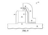
- FIGS. 7-9set forth partial cutaway side views of a wafer 701 at various stages in the manufacture of a spilt gate memory cell with a gap spacer according to another embodiment of the present invention.
- FIG. 7shows a partial side view of wafer 701 after the formation of a gate 707 located over substrate 703 .
- Located on gate 707is a structure of antireflective coating 711 .
- Gate 707is located on dielectric 705 .
- Gate 707 , dielectric 705 , substrate 703 , and structure 711may be made of similar material and/or formed in a similar manner as that set forth above with respect to gate 107 , dielectric 105 , substrate 103 , and structure 111 .
- a dielectric layer 713is formed on wafer 701 .
- layer 713is formed by an oxidation process, but may be formed by a deposition process in other embodiments.
- layer 713is at least 30 A thick and preferably between 100 A and 200 A thick. During the oxidation process, a portion of the side walls of gate 707 and the exposed surface of substrate 703 are oxidized.
- layer 713would be deposited on wafer 701 and may be formed of dielectric materials such as silicon oxide, high K dielectrics (e.g. hafnium oxide), or a nitride.
- FIG. 8shows wafer 701 after a portion of layer 713 has been removed to form gap spacer 801 .
- layer 713is anisotroically etched where etching is stopped when the etchant reaches silicon of substrate 103 .
- Wafer 701is then annealed to reduce plasma induced damage to the exposed portion of substrate 703 from the anisotropic etch.
- the anisotropic etchis a timed etch designed to leave approximately 10-30 A of oxide of layer 713 on substrate 703 .
- Wafer 701is then subjected to an isotropic HF wet etch to remove the remaining portion of the oxide on substrate 703 .
- FIG. 9shows wafer 701 after a layer 903 of charge storage material is formed on wafer 101 and a control gate 901 is formed from a layer of gate material.
- layer 903is formed by forming a tunnel dielectric layer on the tunnel region of substrate 703 having a thickness in a range of e.g. 40-80 A.
- the tunnel dielectric layeris formed by oxidizing exposed portions of substrate 703 . During the oxidation process, the thickness of spacer 801 is increased due to the oxidation of gate 707 .
- the tunnel dielectric layermaybe formed by other processes (e.g. deposition) and be of other materials (e.g. a high K dielectric such as hafnium oxide).
- discrete charge storage elementse.g. silicon nanocrystals
- another dielectric layere.g. a high temperature oxide
- a layer of control gate materialis formed on the charge storage layer 903 , wherein the charge storage layer, the select gate material layer, and structure 711 are patterned to form the structure as shown in FIG. 9 .
- wafer 701may be further processed as described above with respect to wafer 101 .
- spacer 801 on the side wall of gate 707acts to increase the distance between the control gate 901 and select gate 707 . As described above, this acts to improve the reliability of the cell by increasing the breakdown voltage between the control gate and select gate as well as decreasing program disturb of an erased bit cell.
- layer 401(and spacer 801 in some embodiments) is formed by an oxidation of an oxidizable material, it is of a higher quality than a layer formed by a deposition process. Furthermore, because layer 401 is formed by an oxidation of a spacer of oxidizable material, it extends higher up the gate stack (e.g. almost to the top of structure 111 ) as opposed to a spacer formed from an oxidized layer formed on the side wall of the select gate (e.g. see FIG. 8 where spacer 801 does not extend as high up structure 711 as layer 401 extends up on structure 111 ).
- forming a gap spacer by oxidizing a spacer of oxidizable materialmay in some embodiments, allow for the gap spacer to extend higher up the side wall of a control gate to provide for more separation from the top corner of the select gate to the control gate. Furthermore, in some embodiments, forming the spacer by an oxidizing process allows for a gap spacer to be formed without the use of a nitride layer which allows for easier removable of unwanted spacer material. However, some embodiments may use a nitride material.
- a layer located along a sidewallincludes where a layer is formed directly on the sidewall, the layer is formed directly on an intermediate layer that is formed on directly on the side wall, or there are one or more intermediate layers formed along the side wall are located between the layer and the layer formed directly on the sidewall.
- a layermay be located along a side wall if it is formed directly on the side wall or if one or more layers are located between the layer and the sidewall.
- a method for forming a split gate deviceincludes forming a first dielectric layer over a semiconductor layer, forming a first conductive gate layer over the first dielectric layer, and forming a first sidewall of the first conductive gate layer.
- the semiconductor layerincludes a tunnel region which is laterally adjacent the first sidewall of the first conductive gate layer.
- the methodincludes forming a second dielectric layer along the first sidewall of the first conductive gate layer and over the tunnel region of the semiconductor layer and removing a first portion of the second dielectric layer from over the tunnel region. A second portion of the second dielectric layer remains along the first sidewall of the first conductive gate layer.
- the methodincludes after the removing the first portion, forming a third dielectric layer over the tunnel region.
- the methodalso includes after forming the third dielectric layer, forming a charge storage layer over a portion of a top surface of the first conductive gate layer.
- the charge storage layeris located along the first sidewall of the first conductive gate layer and over the tunnel region of the semiconductor layer.
- the methodincludes forming a second conductive gate layer over the charge storage layer.
- the second conductive gate layeris formed over the portion of the top surface of the first conductive gate layer, along the first sidewall of the first conductive gate layer, and over the tunnel region of the semiconductor layer.
- a method for forming a split gate deviceincludes forming a first dielectric layer over a semiconductor layer, forming a first conductive gate layer over the first dielectric layer, and forming a first sidewall of the first conductive gate layer.
- the semiconductor layerincludes a tunnel region which is laterally adjacent the first sidewall of the first conductive gate layer.
- the methodincludes forming second dielectric layer along the first sidewall of the first conductive gate layer, forming an oxidizable layer over the first conductive gate layer and the second dielectric layer. Along the first sidewall of the first conductive gate layer, the second dielectric layer is between the first conductive gate layer and the oxidizable layer.
- the methodincludes removing a portion of the oxidizable layer from over the tunnel region of the semiconductor layer, oxidizing the oxidizable layer to form an oxide layer along the first sidewall of the first conductive gate layer, and forming a charge storage layer over a portion of a top surface of the first conductive gate layer and over the oxide layer.
- the charge storage layeris located along the first sidewall of the first conductive gate layer and over the tunnel region of the semiconductor layer.
- the methodalso includes forming a second conductive gate layer over the charge storage layer. The second conductive gate layer is formed over the portion of the top surface of the first conductive gate layer, along the first sidewall of the first conductive gate layer, and over the tunnel region of the semiconductor layer.
Landscapes
- Non-Volatile Memory (AREA)
- Semiconductor Memories (AREA)
Abstract
Description
- 1. Field of the Invention
- This invention relates to a split gate memory devices and more specifically to gap spacers for a spilt gate memory device.
- 2. Description of the Related Art
- Split gate memory devices are memory device that include transistors having split gates. In one embodiment, a spilt gate transistor includes a control gate and a select gate. Charge is selectively introduced into a charge storage structure of a split gate transistor to store a value (e.g. a “1”) where the lack of charge in the structure is indicative that another value (e.g. a “0”) is stored.
- The present invention may be better understood, and its numerous objects, features, and advantages made apparent to those skilled in the art by referencing the accompanying drawings.
FIGS. 1-6 set forth partial cutaway side views of a memory cell at various stages in its manufacture according to one embodiment of the present invention.FIGS. 7-9 set forth partial cutaway side views of a memory cell at various stages in its manufacture according to another embodiment of the present invention.- The use of the same reference symbols in different drawings indicates identical items unless otherwise noted. The Figures are not necessarily drawn to scale.
- The following sets forth a detailed description of a mode for carrying out the invention. The description is intended to be illustrative of the invention and should not be taken to be limiting.
- It has been discovered that providing a split gate memory cell with a gap spacer between the select gate and control gate may advantageously provide for reduced program disturb and reduced select gate/control gate breakdown in a split gate memory cell.
FIGS. 1-6 set forth partial cross sectional side views of various stages of a wafer in the manufacture of a memory cell with a gap spacer formed by the oxidation of an oxidizable material.- As shown in
FIG. 1 ,wafer 101 includes asemiconductor substrate 103. In one embodiment,substrate 103 is made of single crystal silicon and may be doped with impurities. In other embodiments,substrate 103 may be made of other types of semiconductor materials e.g. silicon germanium, silicon carbon, or a III-V semiconductor material. In one embodiment,substrate 103 is made of a bulk semiconductor material (e.g. a bulk substrate semiconductor layer), but may have other configurations in other embodiments (e.g. a semiconductor on insulator configuration). With a semiconductor on insulator configuration, a semiconductor layer is located on a buried dielectric layer. - A
select gate 107 is formed oversubstrate 103. In one embodiment,gate 107 is made of doped polysilicon, but may be made of other gate materials in other embodiments. In one embodiment,gate 107 has a thickness (e.g. height in the view ofFIG. 1 ) of 1500 Angstroms (A) but may have other thicknesses in other embodiments. A gate dielectric105 is located betweengate 107 andsubstrate 103. Gate dielectric105 has a thickness in the range of 40-80 A, but may be of other thicknesses in other embodiments. Gate dielectric105 is of a dielectric material such as e.g. silicon oxide, hafnium oxide, or other type of high K dielectric material. - Located on top of
gate 107 is adielectric structure 109. In one embodiment,dielectric structure 109 is made of silicon dioxide, but may be made of other materials in other embodiments. In one embodiment,structure 109 has a thickness in the range of 10-100 A, but may have other thicknesses in other embodiments. Astructure 111 of an antireflective coating (ARC) is located onstructure 109. In one embodiment,structure 111 is 200 A is thick but may be of other thicknesses in other embodiments. In one embodiment,structure 111 is made of silicon rich silicon nitride, but may be made of other materials in other embodiments. Some embodiments do not includestructure 109 whereinstructure 111 is located ongate 107. - The stack of dielectric105,
gate 107,structure 109, andstructure 111 are formed by forming layers of those materials oversubstrate 103 and then patterning those layers to leave the stack structures shown inFIG. 1 . In one embodiment, the layers are patterned by forming a patterned photo resist structure over the layers (not shown) and etching the layers with an etchant or etchants having the appropriate etch chemistries. FIG. 2 shows a stage ofwafer 101 after the formation of adielectric layer 201 and anoxidizable layer 203. In one embodiment,layer 201 is made of silicon oxide and is formed by oxidizinggate 107 andsubstrate 103. Exposed silicon portions ofgate 107 andsubstrate 103 are consumed in the oxidation process to makelayer 201.Layer 201 has a thickness controlled by the parameters of the oxidation process (e.g. time, temp, etc). In one embodiment, the thickness oflayer 201 is in the range of 30-100 A, but may be of other thicknesses in other embodiments. In other embodiments,layer 201 may be formed through thermal oxidation or deposition e.g. by furnace and RTA or chemical vapor deposition.- A
layer 203 of oxidizable material is formed onlayer 201 overgate 107 andsubstrate 103 and along the sidewalls ofgate 107. In one embodiment,layer 203 is a made of amorphous silicon, but may be made of other oxidizable materials in other embodiments (e.g. poly silicon). In one embodiment,layer 203 has a thickness in the range of 15-100 A but may be of other thicknesses in other embodiments. In one embodiment, utilizing amorphous silicon may provide for better control of the thickness of the relativelythin layer 203. FIG. 3 showswater 101 at another manufacturing stage wherelayer 203 is anisotropically etched to formspacer 301. In one embodiment,layer 203 is etched with an etchant that is selective to the oxidizable material oflayer 203 and is selective with respect to the material oflayer 201. In one embodiment, an etchant of chlorine, fluorine, and/or bromine-based chemicals is used to remove portions oflayer 203.Layer 201 serves as an etch stop during the anisotropic etching oflayer 203.- After
layer 203 is etched,layer 201 is etched with an etchant that is selective to the material oflayer 201 and is selective with respect to the material ofspacer 301 to remove the exposed portions oflayer 201 and to cleansubstrate 103. In one embodiment, the isotropic etching is performed using an HF etchant. FIG. 4 showswafer 101 after the wafer is subject to an oxidation process wherespacer 301 is oxidized and exposed surfaces ofsubstrate 103 are oxidized to form anoxide layer 401. In one embodiment,layer 401 along the sidewall has a thickness in the range of 40-80 A, but may have other thickness in other embodiments. In one embodiment, the thickness of the portion oflayer 401 along the side wall ofgate 107 is dependent upon the thickness ofspacer 301. Preferably, in some embodiments, the oxidation process is performed for a period of time that is just long enough to oxidize all ofspacer 301.- During the oxidation process, a portion of the
substrate 103 is oxidized as well to form the portion oflayer 401 located onsubstrate 103. In some embodiments, this portion oflayer 401 serves a tunnel dielectric. In other embodiments, an additional dielectric layer may be formed onlayer 401 which also would serve as a tunnel dielectric. In some embodiments,layer 401 may be anisotropically etched to reduce the thickness of the portion oflayer 401 located onsubstrate 103. FIG. 5 is a partial side cutaway view ofwafer 101 after acharge storage layer 501 andcontrol gate 505 are formed overwafer 101 and patterned to leave the structure shown inFIG. 5 . The embodiment shown,layer 501 includes a number of spaced apart discretecharge storage elements 503. In one embodiment, the discretecharge storage elements 503 are made of silicon nanocrystals, but may be made of other types of material such as metal nanoclusters, silicide nanoclusters, or germanium nanocrystals. The discretecharge storage elements 503 are isolated structures that can be programmed to store charge to alter the voltage threshold of the memory cell during a read operation. Accordingly, the value read from the cell during a read operation will depend upon whether the cell is programmed. In the embodiment shown, the discrete charge storage structures that most affect the voltage threshold of the memory cell are located inarea 509.- In the embodiment shown, the
elements 503 are formed onlayer 401 and onARC structure 111. In one example, silicon nanocrystals can be formed by forming a thin layer of silicon overwafer 101 and then annealing the wafer to form the discrete elements. In some embodiments, an additional layer of silicon is formed over the nanocrystals and then annealed to increase the thickness of the nanocrystals. However,elements 503 can be formed by other methods in other embodiments. - After the formation of
discrete elements 503, another layer of dielectric material (e.g. silicon oxide) is formed overwafer 101 to cover the discrete elements. In one embodiment, this dielectric layer has a thickness of 140 A, but it may be of other thicknesses in other embodiments. This top layer is shown inFIG. 5 as being part oflayer 501. - After
layer 501 has been formed, a layer of gate material (e.g. polysilicon) is formed overwafer 101. In one embodiment, the layer of gate material is 1000 A thick, but may be of other thicknesses in other embodiments. Afterwards, the layer of gate material is patterned to formcontrol gate 505. When the control gate layer is patterned,layer 501,structure 111,structure 109,layer 401, andlayer 201 are also patterned with the appropriate etch chemistries to leave the structures shown inFIG. 5 . - In the embodiment shown, the portion of
layer 401 located onsubstrate 103 is used as a tunnel oxide for the memory cell shown inFIG. 5 . FIG. 6 showswafer 101 afterdielectric spacers wafer 101 and aftersource region 607 and drainregion 605 are formed insubstrate 103. In one embodiment,spacers wafer 101 and anisotropically etched to form the spacer structures.Source region 607 and drainregion 605 are formed by implanting those regions with conductivity dopants (e.g. boron, arsenic, phosphorous, indium) that are of an opposite conductivity as the dopants insubstrate 103. In some embodiments, the source and drain regions include lightly doped extension regions that are implanted prior to the formation ofspacer 603. Afterspacer 603 is formed, a heavy dosage of the impurities are implanted intoregions FIG. 6 shows a split gate memory cell having aselect gate 107, acontrol gate 505, asource region 607, adrain region 605, and a charge storage structure (the discrete charge storage elements503). In other embodiments, other types of charge storage structures (e.g. a floating gate) can be used. The spilt gate memory cell includes atunnel region 615 which is the portion of thesubstrate 103 under discretecharge storage elements 503.Tunnel region 615 is located laterally adjacent to theselect gate 107 and located under a portion ofcontrol gate 505. The charge storage structure of the memory cell ofFIG. 6 is programmed, erased, and read by applying the appropriate voltages and coupling the appropriate circuitry to thesource region 607,drain region 605,control gate 505,select gate 607, andsubstrate 103.- After the stage of
FIG. 6 , silicide (not shown) is formed on exposed portions ofsource region 607,drain region 605,control gate 505, andselect gate 107. Contacts and interconnect layers embedded in dielectric material are then formed overwafer 101 to interconnect the structures of the memory cells to structures of other circuitry. For example, drainregion 605 may be coupled to a bit line andselect gate 107 may be coupled to a word line of a memory array. Afterwards, bond pads and a passivation layer may be formed onwafer 101.Wafer 101 is then singulated into multiple integrated circuits with each integrated circuit including multiple memory cells in an array similar to the memory cell shown inFIG. 6 . - In one embodiment, providing a gap spacer (the portion of
layer select gate 107 andcontrol gate 505 acts to improve the reliability of the cell by increasing the breakdown voltage between the control gate and select gate. For example, a high electric field may be present at the location shown byline 611 due to the proximately ofselect gate corner 612. Providing this gap spacer acts to reduce the high field at that location. Also, atlocation 610 ofsubstrate 103, a high peak electric field may cause band to band generation of electrons which can cause program disturb of an erased bit cell. Increasing the gap dielectric thickness (e.g. withlayer 401 and201) decreases the peak electric field in the gap (609) between the select gate and control gate in thesubstrate 103. - Referring back to
FIG. 1 , in another embodiment,gate 107 may be defined in different patterning processes. For example, inFIG. 1 , the layer of gate material would be patterned first to form the right sidewall ofgate 107 shown inFIG. 1 . The left sidewall ofgate 107 would be formed after the formation of thecharge storage layer 501 and the layer of control gate material forgate 505. FIGS. 7-9 set forth partial cutaway side views of awafer 701 at various stages in the manufacture of a spilt gate memory cell with a gap spacer according to another embodiment of the present invention.FIG. 7 shows a partial side view ofwafer 701 after the formation of agate 707 located oversubstrate 703. Located ongate 707 is a structure ofantireflective coating 711.Gate 707 is located on dielectric705.Gate 707, dielectric705,substrate 703, andstructure 711, may be made of similar material and/or formed in a similar manner as that set forth above with respect togate 107, dielectric105,substrate 103, andstructure 111.- A
dielectric layer 713 is formed onwafer 701. In one embodiment,layer 713 is formed by an oxidation process, but may be formed by a deposition process in other embodiments. In one embodiment,layer 713 is at least 30 A thick and preferably between 100 A and 200 A thick. During the oxidation process, a portion of the side walls ofgate 707 and the exposed surface ofsubstrate 703 are oxidized. In some embodiments,layer 713 would be deposited onwafer 701 and may be formed of dielectric materials such as silicon oxide, high K dielectrics (e.g. hafnium oxide), or a nitride. FIG. 8 showswafer 701 after a portion oflayer 713 has been removed to formgap spacer 801. In one embodiment,layer 713 is anisotroically etched where etching is stopped when the etchant reaches silicon ofsubstrate 103.Wafer 701 is then annealed to reduce plasma induced damage to the exposed portion ofsubstrate 703 from the anisotropic etch. In another embodiment, the anisotropic etch is a timed etch designed to leave approximately 10-30 A of oxide oflayer 713 onsubstrate 703.Wafer 701 is then subjected to an isotropic HF wet etch to remove the remaining portion of the oxide onsubstrate 703.FIG. 9 showswafer 701 after a layer903 of charge storage material is formed onwafer 101 and acontrol gate 901 is formed from a layer of gate material. In the embodiment shown, layer903 is formed by forming a tunnel dielectric layer on the tunnel region ofsubstrate 703 having a thickness in a range of e.g. 40-80 A. In one embodiment, the tunnel dielectric layer is formed by oxidizing exposed portions ofsubstrate 703. During the oxidation process, the thickness ofspacer 801 is increased due to the oxidation ofgate 707. In other embodiments, the tunnel dielectric layer maybe formed by other processes (e.g. deposition) and be of other materials (e.g. a high K dielectric such as hafnium oxide). Afterwards, discrete charge storage elements (e.g. silicon nanocrystals) are formed on the tunnel dielectric,spacer 801, andstructure 711. Afterwards, another dielectric layer (e.g. a high temperature oxide) is formed on the discretecharge storage elements 904 and exposed portion of the tunnel dielectric to complete charge storage layer903.- Afterwards, a layer of control gate material is formed on the charge storage layer903, wherein the charge storage layer, the select gate material layer, and
structure 711 are patterned to form the structure as shown inFIG. 9 . Afterwards,wafer 701 may be further processed as described above with respect towafer 101. - As with
layers gate 107,spacer 801 on the side wall ofgate 707 acts to increase the distance between thecontrol gate 901 andselect gate 707. As described above, this acts to improve the reliability of the cell by increasing the breakdown voltage between the control gate and select gate as well as decreasing program disturb of an erased bit cell. - Referring back to
FIG. 4 , because layer401 (andspacer 801 in some embodiments) is formed by an oxidation of an oxidizable material, it is of a higher quality than a layer formed by a deposition process. Furthermore, becauselayer 401 is formed by an oxidation of a spacer of oxidizable material, it extends higher up the gate stack (e.g. almost to the top of structure111) as opposed to a spacer formed from an oxidized layer formed on the side wall of the select gate (e.g. seeFIG. 8 wherespacer 801 does not extend as high upstructure 711 aslayer 401 extends up on structure111). Accordingly, forming a gap spacer by oxidizing a spacer of oxidizable material may in some embodiments, allow for the gap spacer to extend higher up the side wall of a control gate to provide for more separation from the top corner of the select gate to the control gate. Furthermore, in some embodiments, forming the spacer by an oxidizing process allows for a gap spacer to be formed without the use of a nitride layer which allows for easier removable of unwanted spacer material. However, some embodiments may use a nitride material. - As used herein a layer located along a sidewall includes where a layer is formed directly on the sidewall, the layer is formed directly on an intermediate layer that is formed on directly on the side wall, or there are one or more intermediate layers formed along the side wall are located between the layer and the layer formed directly on the sidewall. For example, a layer may be located along a side wall if it is formed directly on the side wall or if one or more layers are located between the layer and the sidewall.
- In one embodiment, a method for forming a split gate device includes forming a first dielectric layer over a semiconductor layer, forming a first conductive gate layer over the first dielectric layer, and forming a first sidewall of the first conductive gate layer. The semiconductor layer includes a tunnel region which is laterally adjacent the first sidewall of the first conductive gate layer. The method includes forming a second dielectric layer along the first sidewall of the first conductive gate layer and over the tunnel region of the semiconductor layer and removing a first portion of the second dielectric layer from over the tunnel region. A second portion of the second dielectric layer remains along the first sidewall of the first conductive gate layer. The method includes after the removing the first portion, forming a third dielectric layer over the tunnel region. The method also includes after forming the third dielectric layer, forming a charge storage layer over a portion of a top surface of the first conductive gate layer. The charge storage layer is located along the first sidewall of the first conductive gate layer and over the tunnel region of the semiconductor layer. The method includes forming a second conductive gate layer over the charge storage layer. The second conductive gate layer is formed over the portion of the top surface of the first conductive gate layer, along the first sidewall of the first conductive gate layer, and over the tunnel region of the semiconductor layer.
- In one embodiment, a method for forming a split gate device includes forming a first dielectric layer over a semiconductor layer, forming a first conductive gate layer over the first dielectric layer, and forming a first sidewall of the first conductive gate layer. The semiconductor layer includes a tunnel region which is laterally adjacent the first sidewall of the first conductive gate layer. The method includes forming second dielectric layer along the first sidewall of the first conductive gate layer, forming an oxidizable layer over the first conductive gate layer and the second dielectric layer. Along the first sidewall of the first conductive gate layer, the second dielectric layer is between the first conductive gate layer and the oxidizable layer. The method includes removing a portion of the oxidizable layer from over the tunnel region of the semiconductor layer, oxidizing the oxidizable layer to form an oxide layer along the first sidewall of the first conductive gate layer, and forming a charge storage layer over a portion of a top surface of the first conductive gate layer and over the oxide layer. The charge storage layer is located along the first sidewall of the first conductive gate layer and over the tunnel region of the semiconductor layer. The method also includes forming a second conductive gate layer over the charge storage layer. The second conductive gate layer is formed over the portion of the top surface of the first conductive gate layer, along the first sidewall of the first conductive gate layer, and over the tunnel region of the semiconductor layer.
- While particular embodiments of the present invention have been shown and described, it will be recognized to those skilled in the art that, based upon the teachings herein, further changes and modifications may be made without departing from this invention and its broader aspects, and thus, the appended claims are to encompass within their scope all such changes and modifications as are within the true spirit and scope of this invention.
Claims (21)
Priority Applications (1)
| Application Number | Priority Date | Filing Date | Title |
|---|---|---|---|
| US13/961,574US8835295B2 (en) | 2011-09-29 | 2013-08-07 | Split gate memory device with gap spacer |
Applications Claiming Priority (2)
| Application Number | Priority Date | Filing Date | Title |
|---|---|---|---|
| US13/248,549US20130084697A1 (en) | 2011-09-29 | 2011-09-29 | Split gate memory device with gap spacer |
| US13/961,574US8835295B2 (en) | 2011-09-29 | 2013-08-07 | Split gate memory device with gap spacer |
Related Parent Applications (1)
| Application Number | Title | Priority Date | Filing Date |
|---|---|---|---|
| US13/248,549ContinuationUS20130084697A1 (en) | 2011-09-29 | 2011-09-29 | Split gate memory device with gap spacer |
Publications (2)
| Publication Number | Publication Date |
|---|---|
| US20130323922A1true US20130323922A1 (en) | 2013-12-05 |
| US8835295B2 US8835295B2 (en) | 2014-09-16 |
Family
ID=47992952
Family Applications (2)
| Application Number | Title | Priority Date | Filing Date |
|---|---|---|---|
| US13/248,549AbandonedUS20130084697A1 (en) | 2011-09-29 | 2011-09-29 | Split gate memory device with gap spacer |
| US13/961,574Active2031-10-31US8835295B2 (en) | 2011-09-29 | 2013-08-07 | Split gate memory device with gap spacer |
Family Applications Before (1)
| Application Number | Title | Priority Date | Filing Date |
|---|---|---|---|
| US13/248,549AbandonedUS20130084697A1 (en) | 2011-09-29 | 2011-09-29 | Split gate memory device with gap spacer |
Country Status (1)
| Country | Link |
|---|---|
| US (2) | US20130084697A1 (en) |
Cited By (25)
| Publication number | Priority date | Publication date | Assignee | Title |
|---|---|---|---|---|
| US20140124847A1 (en)* | 2012-11-07 | 2014-05-08 | Huilong Zhu | Semiconductor devices and methods for manufacturing the same |
| US8871598B1 (en) | 2013-07-31 | 2014-10-28 | Freescale Semiconductor, Inc. | Non-volatile memory (NVM) and high-k and metal gate integration using gate-first methodology |
| US8877585B1 (en) | 2013-08-16 | 2014-11-04 | Freescale Semiconductor, Inc. | Non-volatile memory (NVM) cell, high voltage transistor, and high-K and metal gate transistor integration |
| US8877568B2 (en) | 2010-10-29 | 2014-11-04 | Freescale Semiconductor, Inc. | Methods of making logic transistors and non-volatile memory cells |
| US8901632B1 (en) | 2013-09-30 | 2014-12-02 | Freescale Semiconductor, Inc. | Non-volatile memory (NVM) and high-K and metal gate integration using gate-last methodology |
| US8906764B2 (en) | 2012-01-04 | 2014-12-09 | Freescale Semiconductor, Inc. | Non-volatile memory (NVM) and logic integration |
| US20150001612A1 (en)* | 2013-06-27 | 2015-01-01 | Cheong Min Hong | Non-volatile memory (nvm) and high voltage transistor integration |
| US8932925B1 (en) | 2013-08-22 | 2015-01-13 | Freescale Semiconductor, Inc. | Split-gate non-volatile memory (NVM) cell and device structure integration |
| US8951863B2 (en) | 2012-04-06 | 2015-02-10 | Freescale Semiconductor, Inc. | Non-volatile memory (NVM) and logic integration |
| US9082837B2 (en) | 2013-08-08 | 2015-07-14 | Freescale Semiconductor, Inc. | Nonvolatile memory bitcell with inlaid high k metal select gate |
| US9082650B2 (en) | 2013-08-21 | 2015-07-14 | Freescale Semiconductor, Inc. | Integrated split gate non-volatile memory cell and logic structure |
| US9087913B2 (en) | 2012-04-09 | 2015-07-21 | Freescale Semiconductor, Inc. | Integration technique using thermal oxide select gate dielectric for select gate and apartial replacement gate for logic |
| US9112056B1 (en) | 2014-03-28 | 2015-08-18 | Freescale Semiconductor, Inc. | Method for forming a split-gate device |
| US9111865B2 (en) | 2012-10-26 | 2015-08-18 | Freescale Semiconductor, Inc. | Method of making a logic transistor and a non-volatile memory (NVM) cell |
| US9129996B2 (en) | 2013-07-31 | 2015-09-08 | Freescale Semiconductor, Inc. | Non-volatile memory (NVM) cell and high-K and metal gate transistor integration |
| US9129855B2 (en) | 2013-09-30 | 2015-09-08 | Freescale Semiconductor, Inc. | Non-volatile memory (NVM) and high-k and metal gate integration using gate-first methodology |
| US9136129B2 (en) | 2013-09-30 | 2015-09-15 | Freescale Semiconductor, Inc. | Non-volatile memory (NVM) and high-k and metal gate integration using gate-last methodology |
| US9231077B2 (en) | 2014-03-03 | 2016-01-05 | Freescale Semiconductor, Inc. | Method of making a logic transistor and non-volatile memory (NVM) cell |
| US9252246B2 (en) | 2013-08-21 | 2016-02-02 | Freescale Semiconductor, Inc. | Integrated split gate non-volatile memory cell and logic device |
| US9257445B2 (en) | 2014-05-30 | 2016-02-09 | Freescale Semiconductor, Inc. | Method of making a split gate non-volatile memory (NVM) cell and a logic transistor |
| US9275864B2 (en) | 2013-08-22 | 2016-03-01 | Freescale Semiconductor,Inc. | Method to form a polysilicon nanocrystal thin film storage bitcell within a high k metal gate platform technology using a gate last process to form transistor gates |
| US9343314B2 (en) | 2014-05-30 | 2016-05-17 | Freescale Semiconductor, Inc. | Split gate nanocrystal memory integration |
| US9379222B2 (en) | 2014-05-30 | 2016-06-28 | Freescale Semiconductor, Inc. | Method of making a split gate non-volatile memory (NVM) cell |
| US9472418B2 (en) | 2014-03-28 | 2016-10-18 | Freescale Semiconductor, Inc. | Method for forming a split-gate device |
| CN110875389A (en)* | 2018-08-31 | 2020-03-10 | 立锜科技股份有限公司 | MOS element capable of reducing on-resistance and manufacturing method thereof |
Families Citing this family (5)
| Publication number | Priority date | Publication date | Assignee | Title |
|---|---|---|---|---|
| US20140357072A1 (en)* | 2013-05-31 | 2014-12-04 | Jinmiao J. Shen | Methods and structures for split gate memory |
| US9660106B2 (en)* | 2014-08-18 | 2017-05-23 | United Microelectronics Corp. | Flash memory and method of manufacturing the same |
| US9590059B2 (en)* | 2014-12-24 | 2017-03-07 | Taiwan Semiconductor Manufacturing Co., Ltd. | Interdigitated capacitor to integrate with flash memory |
| US10879181B2 (en)* | 2016-11-28 | 2020-12-29 | Taiwan Semiconductor Manufacturing Co., Ltd. | Embedded non-volatile memory with side word line |
| US11877456B2 (en)* | 2020-09-15 | 2024-01-16 | Ememory Technology Inc. | Memory cell of non-volatile memory |
Family Cites Families (5)
| Publication number | Priority date | Publication date | Assignee | Title |
|---|---|---|---|---|
| US20020197790A1 (en)* | 1997-12-22 | 2002-12-26 | Kizilyalli Isik C. | Method of making a compound, high-K, gate and capacitor insulator layer |
| US7361543B2 (en)* | 2004-11-12 | 2008-04-22 | Freescale Semiconductor, Inc. | Method of forming a nanocluster charge storage device |
| US7456465B2 (en)* | 2005-09-30 | 2008-11-25 | Freescale Semiconductor, Inc. | Split gate memory cell and method therefor |
| US7811886B2 (en) | 2007-02-06 | 2010-10-12 | Freescale Semiconductor, Inc. | Split-gate thin film storage NVM cell with reduced load-up/trap-up effects |
| US8178406B2 (en)* | 2007-10-29 | 2012-05-15 | Freescale Semiconductor, Inc. | Split gate device and method for forming |
- 2011
- 2011-09-29USUS13/248,549patent/US20130084697A1/ennot_activeAbandoned
- 2013
- 2013-08-07USUS13/961,574patent/US8835295B2/enactiveActive
Cited By (27)
| Publication number | Priority date | Publication date | Assignee | Title |
|---|---|---|---|---|
| US8877568B2 (en) | 2010-10-29 | 2014-11-04 | Freescale Semiconductor, Inc. | Methods of making logic transistors and non-volatile memory cells |
| US8906764B2 (en) | 2012-01-04 | 2014-12-09 | Freescale Semiconductor, Inc. | Non-volatile memory (NVM) and logic integration |
| US8951863B2 (en) | 2012-04-06 | 2015-02-10 | Freescale Semiconductor, Inc. | Non-volatile memory (NVM) and logic integration |
| US9087913B2 (en) | 2012-04-09 | 2015-07-21 | Freescale Semiconductor, Inc. | Integration technique using thermal oxide select gate dielectric for select gate and apartial replacement gate for logic |
| US9111865B2 (en) | 2012-10-26 | 2015-08-18 | Freescale Semiconductor, Inc. | Method of making a logic transistor and a non-volatile memory (NVM) cell |
| US9331182B2 (en)* | 2012-11-07 | 2016-05-03 | Institute of Microelectronics, Chinese Academy of Sciences | Semiconductor devices with a gate conductor formed as a spacer, and methods for manufacturing the same |
| US20140124847A1 (en)* | 2012-11-07 | 2014-05-08 | Huilong Zhu | Semiconductor devices and methods for manufacturing the same |
| US20150001612A1 (en)* | 2013-06-27 | 2015-01-01 | Cheong Min Hong | Non-volatile memory (nvm) and high voltage transistor integration |
| US9006093B2 (en)* | 2013-06-27 | 2015-04-14 | Freescale Semiconductor, Inc. | Non-volatile memory (NVM) and high voltage transistor integration |
| US8871598B1 (en) | 2013-07-31 | 2014-10-28 | Freescale Semiconductor, Inc. | Non-volatile memory (NVM) and high-k and metal gate integration using gate-first methodology |
| US9129996B2 (en) | 2013-07-31 | 2015-09-08 | Freescale Semiconductor, Inc. | Non-volatile memory (NVM) cell and high-K and metal gate transistor integration |
| US9082837B2 (en) | 2013-08-08 | 2015-07-14 | Freescale Semiconductor, Inc. | Nonvolatile memory bitcell with inlaid high k metal select gate |
| US8877585B1 (en) | 2013-08-16 | 2014-11-04 | Freescale Semiconductor, Inc. | Non-volatile memory (NVM) cell, high voltage transistor, and high-K and metal gate transistor integration |
| US9252246B2 (en) | 2013-08-21 | 2016-02-02 | Freescale Semiconductor, Inc. | Integrated split gate non-volatile memory cell and logic device |
| US9082650B2 (en) | 2013-08-21 | 2015-07-14 | Freescale Semiconductor, Inc. | Integrated split gate non-volatile memory cell and logic structure |
| US9275864B2 (en) | 2013-08-22 | 2016-03-01 | Freescale Semiconductor,Inc. | Method to form a polysilicon nanocrystal thin film storage bitcell within a high k metal gate platform technology using a gate last process to form transistor gates |
| US8932925B1 (en) | 2013-08-22 | 2015-01-13 | Freescale Semiconductor, Inc. | Split-gate non-volatile memory (NVM) cell and device structure integration |
| US9129855B2 (en) | 2013-09-30 | 2015-09-08 | Freescale Semiconductor, Inc. | Non-volatile memory (NVM) and high-k and metal gate integration using gate-first methodology |
| US9136129B2 (en) | 2013-09-30 | 2015-09-15 | Freescale Semiconductor, Inc. | Non-volatile memory (NVM) and high-k and metal gate integration using gate-last methodology |
| US8901632B1 (en) | 2013-09-30 | 2014-12-02 | Freescale Semiconductor, Inc. | Non-volatile memory (NVM) and high-K and metal gate integration using gate-last methodology |
| US9231077B2 (en) | 2014-03-03 | 2016-01-05 | Freescale Semiconductor, Inc. | Method of making a logic transistor and non-volatile memory (NVM) cell |
| US9112056B1 (en) | 2014-03-28 | 2015-08-18 | Freescale Semiconductor, Inc. | Method for forming a split-gate device |
| US9472418B2 (en) | 2014-03-28 | 2016-10-18 | Freescale Semiconductor, Inc. | Method for forming a split-gate device |
| US9257445B2 (en) | 2014-05-30 | 2016-02-09 | Freescale Semiconductor, Inc. | Method of making a split gate non-volatile memory (NVM) cell and a logic transistor |
| US9343314B2 (en) | 2014-05-30 | 2016-05-17 | Freescale Semiconductor, Inc. | Split gate nanocrystal memory integration |
| US9379222B2 (en) | 2014-05-30 | 2016-06-28 | Freescale Semiconductor, Inc. | Method of making a split gate non-volatile memory (NVM) cell |
| CN110875389A (en)* | 2018-08-31 | 2020-03-10 | 立锜科技股份有限公司 | MOS element capable of reducing on-resistance and manufacturing method thereof |
Also Published As
| Publication number | Publication date |
|---|---|
| US8835295B2 (en) | 2014-09-16 |
| US20130084697A1 (en) | 2013-04-04 |
Similar Documents
| Publication | Publication Date | Title |
|---|---|---|
| US8835295B2 (en) | Split gate memory device with gap spacer | |
| US7416945B1 (en) | Method for forming a split gate memory device | |
| US7811886B2 (en) | Split-gate thin film storage NVM cell with reduced load-up/trap-up effects | |
| CN101030602B (en) | MOS transistor for decreasing short channel and its production | |
| JP5806439B2 (en) | Memory cell and manufacturing method thereof | |
| CN107305892B (en) | Method of Forming Tri-Gate Non-Volatile Flash Memory Cell Pairs Using Two Polysilicon Deposition Steps | |
| US9711513B2 (en) | Semiconductor structure including a nonvolatile memory cell and method for the formation thereof | |
| US8530950B1 (en) | Methods and structures for split gate memory | |
| CN110164767B (en) | Semiconductor device and method of forming the same | |
| US10153349B2 (en) | Methods and structures for a split gate memory cell structure | |
| US9418864B2 (en) | Method of forming a non volatile memory device using wet etching | |
| US9343466B1 (en) | Methods for fabricating flash memory cells and integrated circuits having flash memory cells embedded with logic | |
| KR100799030B1 (en) | Manufacturing Method of NAND Flash Memory Device | |
| US9748111B2 (en) | Method of fabricating semiconductor structure using planarization process and cleaning process | |
| KR100714473B1 (en) | Nonvolatile memory device and method of fabricating the same | |
| JP2008244108A (en) | Semiconductor device and manufacturing method of semiconductor device | |
| US9437705B2 (en) | Method of manufacturing a spacer for dual gate electronic memory cell and associated electronic memory cell | |
| US7301193B2 (en) | Structure and method for low Vss resistance and reduced DIBL in a floating gate memory cell | |
| JP2011040782A (en) | Method of manufacturing semiconductor device | |
| CN107579108B (en) | Method for forming semiconductor structure | |
| CN104701262A (en) | Formation method of semiconductor device | |
| CN109671777B (en) | Semiconductor structure and method of forming the same | |
| US20070007578A1 (en) | Sub zero spacer for shallow MDD junction to improve BVDSS in NVM bitcell | |
| TWI534959B (en) | Non-volatile memory and the manufacturing method thereof | |
| TWI493660B (en) | Non-volatile memory and manufacturing method thereof |
Legal Events
| Date | Code | Title | Description |
|---|---|---|---|
| AS | Assignment | Owner name:CITIBANK, N.A., AS NOTES COLLATERAL AGENT, NEW YORK Free format text:SECURITY AGREEMENT;ASSIGNOR:FREESCALE SEMICONDUCTOR, INC.;REEL/FRAME:031591/0266 Effective date:20131101 Owner name:CITIBANK, N.A., AS NOTES COLLATERAL AGENT, NEW YOR Free format text:SECURITY AGREEMENT;ASSIGNOR:FREESCALE SEMICONDUCTOR, INC.;REEL/FRAME:031591/0266 Effective date:20131101 | |
| AS | Assignment | Owner name:CITIBANK, N.A., AS COLLATERAL AGENT, NEW YORK Free format text:SUPPLEMENT TO IP SECURITY AGREEMENT;ASSIGNOR:FREESCALE SEMICONDUCTOR, INC.;REEL/FRAME:031627/0158 Effective date:20131101 Owner name:CITIBANK, N.A., AS NOTES COLLATERAL AGENT, NEW YOR Free format text:SUPPLEMENT TO IP SECURITY AGREEMENT;ASSIGNOR:FREESCALE SEMICONDUCTOR, INC.;REEL/FRAME:031627/0201 Effective date:20131101 | |
| STCF | Information on status: patent grant | Free format text:PATENTED CASE | |
| AS | Assignment | Owner name:FREESCALE SEMICONDUCTOR, INC., TEXAS Free format text:PATENT RELEASE;ASSIGNOR:CITIBANK, N.A., AS COLLATERAL AGENT;REEL/FRAME:037357/0874 Effective date:20151207 | |
| AS | Assignment | Owner name:MORGAN STANLEY SENIOR FUNDING, INC., MARYLAND Free format text:ASSIGNMENT AND ASSUMPTION OF SECURITY INTEREST IN PATENTS;ASSIGNOR:CITIBANK, N.A.;REEL/FRAME:037444/0787 Effective date:20151207 | |
| AS | Assignment | Owner name:MORGAN STANLEY SENIOR FUNDING, INC., MARYLAND Free format text:ASSIGNMENT AND ASSUMPTION OF SECURITY INTEREST IN PATENTS;ASSIGNOR:CITIBANK, N.A.;REEL/FRAME:037518/0292 Effective date:20151207 | |
| AS | Assignment | Owner name:MORGAN STANLEY SENIOR FUNDING, INC., MARYLAND Free format text:SECURITY AGREEMENT SUPPLEMENT;ASSIGNOR:NXP B.V.;REEL/FRAME:038017/0058 Effective date:20160218 | |
| AS | Assignment | Owner name:MORGAN STANLEY SENIOR FUNDING, INC., MARYLAND Free format text:CORRECTIVE ASSIGNMENT TO CORRECT THE REMOVE APPLICATION 12092129 PREVIOUSLY RECORDED ON REEL 038017 FRAME 0058. ASSIGNOR(S) HEREBY CONFIRMS THE SECURITY AGREEMENT SUPPLEMENT;ASSIGNOR:NXP B.V.;REEL/FRAME:039361/0212 Effective date:20160218 | |
| AS | Assignment | Owner name:NXP, B.V., F/K/A FREESCALE SEMICONDUCTOR, INC., NETHERLANDS Free format text:RELEASE BY SECURED PARTY;ASSIGNOR:MORGAN STANLEY SENIOR FUNDING, INC.;REEL/FRAME:040925/0001 Effective date:20160912 Owner name:NXP, B.V., F/K/A FREESCALE SEMICONDUCTOR, INC., NE Free format text:RELEASE BY SECURED PARTY;ASSIGNOR:MORGAN STANLEY SENIOR FUNDING, INC.;REEL/FRAME:040925/0001 Effective date:20160912 | |
| AS | Assignment | Owner name:MORGAN STANLEY SENIOR FUNDING, INC., MARYLAND Free format text:CORRECTIVE ASSIGNMENT TO CORRECT THE INCORRECT PCT NUMBERS IB2013000664, US2013051970, US201305935 PREVIOUSLY RECORDED AT REEL: 037444 FRAME: 0787. ASSIGNOR(S) HEREBY CONFIRMS THE ASSIGNMENT AND ASSUMPTION OF SECURITY INTEREST IN PATENTS;ASSIGNOR:CITIBANK, N.A.;REEL/FRAME:040450/0715 Effective date:20151207 | |
| AS | Assignment | Owner name:NXP B.V., NETHERLANDS Free format text:RELEASE BY SECURED PARTY;ASSIGNOR:MORGAN STANLEY SENIOR FUNDING, INC.;REEL/FRAME:040928/0001 Effective date:20160622 | |
| AS | Assignment | Owner name:NXP USA, INC., TEXAS Free format text:MERGER;ASSIGNOR:FREESCALE SEMICONDUCTOR, INC.;REEL/FRAME:041144/0363 Effective date:20161107 | |
| AS | Assignment | Owner name:MORGAN STANLEY SENIOR FUNDING, INC., MARYLAND Free format text:CORRECTIVE ASSIGNMENT TO CORRECT THE REMOVE PATENTS 8108266 AND 8062324 AND REPLACE THEM WITH 6108266 AND 8060324 PREVIOUSLY RECORDED ON REEL 037518 FRAME 0292. ASSIGNOR(S) HEREBY CONFIRMS THE ASSIGNMENT AND ASSUMPTION OF SECURITY INTEREST IN PATENTS;ASSIGNOR:CITIBANK, N.A.;REEL/FRAME:041703/0536 Effective date:20151207 | |
| AS | Assignment | Owner name:MORGAN STANLEY SENIOR FUNDING, INC., MARYLAND Free format text:CORRECTIVE ASSIGNMENT TO CORRECT THE REMOVE APPLICATION 12681366 PREVIOUSLY RECORDED ON REEL 039361 FRAME 0212. ASSIGNOR(S) HEREBY CONFIRMS THE SECURITY AGREEMENT SUPPLEMENT;ASSIGNOR:NXP B.V.;REEL/FRAME:042762/0145 Effective date:20160218 Owner name:MORGAN STANLEY SENIOR FUNDING, INC., MARYLAND Free format text:CORRECTIVE ASSIGNMENT TO CORRECT THE REMOVE APPLICATION 12681366 PREVIOUSLY RECORDED ON REEL 038017 FRAME 0058. ASSIGNOR(S) HEREBY CONFIRMS THE SECURITY AGREEMENT SUPPLEMENT;ASSIGNOR:NXP B.V.;REEL/FRAME:042985/0001 Effective date:20160218 | |
| AS | Assignment | Owner name:FREESCALE SEMICONDUCTOR, INC., TEXAS Free format text:ASSIGNMENT OF ASSIGNORS INTEREST;ASSIGNORS:SHEN, JINMIAO J.;CHANG, KO-MIN;WINSTEAD, BRIAN A.;REEL/FRAME:043478/0229 Effective date:20110927 | |
| MAFP | Maintenance fee payment | Free format text:PAYMENT OF MAINTENANCE FEE, 4TH YEAR, LARGE ENTITY (ORIGINAL EVENT CODE: M1551) Year of fee payment:4 | |
| AS | Assignment | Owner name:SHENZHEN XINGUODU TECHNOLOGY CO., LTD., CHINA Free format text:CORRECTIVE ASSIGNMENT TO CORRECT THE TO CORRECT THE APPLICATION NO. FROM 13,883,290 TO 13,833,290 PREVIOUSLY RECORDED ON REEL 041703 FRAME 0536. ASSIGNOR(S) HEREBY CONFIRMS THE THE ASSIGNMENT AND ASSUMPTION OF SECURITYINTEREST IN PATENTS.;ASSIGNOR:MORGAN STANLEY SENIOR FUNDING, INC.;REEL/FRAME:048734/0001 Effective date:20190217 | |
| AS | Assignment | Owner name:NXP B.V., NETHERLANDS Free format text:RELEASE BY SECURED PARTY;ASSIGNOR:MORGAN STANLEY SENIOR FUNDING, INC.;REEL/FRAME:050745/0001 Effective date:20190903 | |
| AS | Assignment | Owner name:MORGAN STANLEY SENIOR FUNDING, INC., MARYLAND Free format text:CORRECTIVE ASSIGNMENT TO CORRECT THE REMOVE APPLICATION 12298143 PREVIOUSLY RECORDED ON REEL 042762 FRAME 0145. ASSIGNOR(S) HEREBY CONFIRMS THE SECURITY AGREEMENT SUPPLEMENT;ASSIGNOR:NXP B.V.;REEL/FRAME:051145/0184 Effective date:20160218 Owner name:MORGAN STANLEY SENIOR FUNDING, INC., MARYLAND Free format text:CORRECTIVE ASSIGNMENT TO CORRECT THE REMOVE APPLICATION 12298143 PREVIOUSLY RECORDED ON REEL 039361 FRAME 0212. ASSIGNOR(S) HEREBY CONFIRMS THE SECURITY AGREEMENT SUPPLEMENT;ASSIGNOR:NXP B.V.;REEL/FRAME:051029/0387 Effective date:20160218 Owner name:MORGAN STANLEY SENIOR FUNDING, INC., MARYLAND Free format text:CORRECTIVE ASSIGNMENT TO CORRECT THE REMOVE APPLICATION 12298143 PREVIOUSLY RECORDED ON REEL 042985 FRAME 0001. ASSIGNOR(S) HEREBY CONFIRMS THE SECURITY AGREEMENT SUPPLEMENT;ASSIGNOR:NXP B.V.;REEL/FRAME:051029/0001 Effective date:20160218 Owner name:MORGAN STANLEY SENIOR FUNDING, INC., MARYLAND Free format text:CORRECTIVE ASSIGNMENT TO CORRECT THE REMOVE APPLICATION 12298143 PREVIOUSLY RECORDED ON REEL 038017 FRAME 0058. ASSIGNOR(S) HEREBY CONFIRMS THE SECURITY AGREEMENT SUPPLEMENT;ASSIGNOR:NXP B.V.;REEL/FRAME:051030/0001 Effective date:20160218 Owner name:MORGAN STANLEY SENIOR FUNDING, INC., MARYLAND Free format text:CORRECTIVE ASSIGNMENT TO CORRECT THE REMOVE APPLICATION12298143 PREVIOUSLY RECORDED ON REEL 042985 FRAME 0001. ASSIGNOR(S) HEREBY CONFIRMS THE SECURITY AGREEMENT SUPPLEMENT;ASSIGNOR:NXP B.V.;REEL/FRAME:051029/0001 Effective date:20160218 Owner name:MORGAN STANLEY SENIOR FUNDING, INC., MARYLAND Free format text:CORRECTIVE ASSIGNMENT TO CORRECT THE REMOVE APPLICATION12298143 PREVIOUSLY RECORDED ON REEL 039361 FRAME 0212. ASSIGNOR(S) HEREBY CONFIRMS THE SECURITY AGREEMENT SUPPLEMENT;ASSIGNOR:NXP B.V.;REEL/FRAME:051029/0387 Effective date:20160218 Owner name:MORGAN STANLEY SENIOR FUNDING, INC., MARYLAND Free format text:CORRECTIVE ASSIGNMENT TO CORRECT THE REMOVE APPLICATION12298143 PREVIOUSLY RECORDED ON REEL 042762 FRAME 0145. ASSIGNOR(S) HEREBY CONFIRMS THE SECURITY AGREEMENT SUPPLEMENT;ASSIGNOR:NXP B.V.;REEL/FRAME:051145/0184 Effective date:20160218 | |
| AS | Assignment | Owner name:NXP B.V., NETHERLANDS Free format text:CORRECTIVE ASSIGNMENT TO CORRECT THE REMOVEAPPLICATION 11759915 AND REPLACE IT WITH APPLICATION11759935 PREVIOUSLY RECORDED ON REEL 040928 FRAME 0001. ASSIGNOR(S) HEREBY CONFIRMS THE RELEASE OF SECURITYINTEREST;ASSIGNOR:MORGAN STANLEY SENIOR FUNDING, INC.;REEL/FRAME:052915/0001 Effective date:20160622 | |
| AS | Assignment | Owner name:NXP, B.V. F/K/A FREESCALE SEMICONDUCTOR, INC., NETHERLANDS Free format text:CORRECTIVE ASSIGNMENT TO CORRECT THE REMOVEAPPLICATION 11759915 AND REPLACE IT WITH APPLICATION11759935 PREVIOUSLY RECORDED ON REEL 040925 FRAME 0001. ASSIGNOR(S) HEREBY CONFIRMS THE RELEASE OF SECURITYINTEREST;ASSIGNOR:MORGAN STANLEY SENIOR FUNDING, INC.;REEL/FRAME:052917/0001 Effective date:20160912 | |
| MAFP | Maintenance fee payment | Free format text:PAYMENT OF MAINTENANCE FEE, 8TH YEAR, LARGE ENTITY (ORIGINAL EVENT CODE: M1552); ENTITY STATUS OF PATENT OWNER: LARGE ENTITY Year of fee payment:8 |