US20130284374A1 - High temperature electrostatic chuck with real-time heat zone regulating capability - Google Patents
High temperature electrostatic chuck with real-time heat zone regulating capabilityDownload PDFInfo
- Publication number
- US20130284374A1 US20130284374A1US13/793,512US201313793512AUS2013284374A1US 20130284374 A1US20130284374 A1US 20130284374A1US 201313793512 AUS201313793512 AUS 201313793512AUS 2013284374 A1US2013284374 A1US 2013284374A1
- Authority
- US
- United States
- Prior art keywords
- supporting plate
- substrate
- substrate supporting
- shaft
- dielectric
- Prior art date
- Legal status (The legal status is an assumption and is not a legal conclusion. Google has not performed a legal analysis and makes no representation as to the accuracy of the status listed.)
- Granted
Links
Images


Classifications
- H—ELECTRICITY
- H01—ELECTRIC ELEMENTS
- H01L—SEMICONDUCTOR DEVICES NOT COVERED BY CLASS H10
- H01L21/00—Processes or apparatus adapted for the manufacture or treatment of semiconductor or solid state devices or of parts thereof
- H01L21/67—Apparatus specially adapted for handling semiconductor or electric solid state devices during manufacture or treatment thereof; Apparatus specially adapted for handling wafers during manufacture or treatment of semiconductor or electric solid state devices or components ; Apparatus not specifically provided for elsewhere
- H01L21/67005—Apparatus not specifically provided for elsewhere
- H01L21/67011—Apparatus for manufacture or treatment
- H01L21/67098—Apparatus for thermal treatment
- H01L21/67103—Apparatus for thermal treatment mainly by conduction
- H—ELECTRICITY
- H01—ELECTRIC ELEMENTS
- H01L—SEMICONDUCTOR DEVICES NOT COVERED BY CLASS H10
- H01L21/00—Processes or apparatus adapted for the manufacture or treatment of semiconductor or solid state devices or of parts thereof
- H01L21/67—Apparatus specially adapted for handling semiconductor or electric solid state devices during manufacture or treatment thereof; Apparatus specially adapted for handling wafers during manufacture or treatment of semiconductor or electric solid state devices or components ; Apparatus not specifically provided for elsewhere
- H01L21/67005—Apparatus not specifically provided for elsewhere
- H01L21/67011—Apparatus for manufacture or treatment
- H01L21/67098—Apparatus for thermal treatment
- H01L21/67109—Apparatus for thermal treatment mainly by convection
- H—ELECTRICITY
- H01—ELECTRIC ELEMENTS
- H01L—SEMICONDUCTOR DEVICES NOT COVERED BY CLASS H10
- H01L21/00—Processes or apparatus adapted for the manufacture or treatment of semiconductor or solid state devices or of parts thereof
- H01L21/67—Apparatus specially adapted for handling semiconductor or electric solid state devices during manufacture or treatment thereof; Apparatus specially adapted for handling wafers during manufacture or treatment of semiconductor or electric solid state devices or components ; Apparatus not specifically provided for elsewhere
- H01L21/67005—Apparatus not specifically provided for elsewhere
- H01L21/67242—Apparatus for monitoring, sorting or marking
- H01L21/67248—Temperature monitoring
- H—ELECTRICITY
- H01—ELECTRIC ELEMENTS
- H01L—SEMICONDUCTOR DEVICES NOT COVERED BY CLASS H10
- H01L21/00—Processes or apparatus adapted for the manufacture or treatment of semiconductor or solid state devices or of parts thereof
- H01L21/67—Apparatus specially adapted for handling semiconductor or electric solid state devices during manufacture or treatment thereof; Apparatus specially adapted for handling wafers during manufacture or treatment of semiconductor or electric solid state devices or components ; Apparatus not specifically provided for elsewhere
- H01L21/683—Apparatus specially adapted for handling semiconductor or electric solid state devices during manufacture or treatment thereof; Apparatus specially adapted for handling wafers during manufacture or treatment of semiconductor or electric solid state devices or components ; Apparatus not specifically provided for elsewhere for supporting or gripping
- H01L21/6831—Apparatus specially adapted for handling semiconductor or electric solid state devices during manufacture or treatment thereof; Apparatus specially adapted for handling wafers during manufacture or treatment of semiconductor or electric solid state devices or components ; Apparatus not specifically provided for elsewhere for supporting or gripping using electrostatic chucks
- H—ELECTRICITY
- H01—ELECTRIC ELEMENTS
- H01L—SEMICONDUCTOR DEVICES NOT COVERED BY CLASS H10
- H01L21/00—Processes or apparatus adapted for the manufacture or treatment of semiconductor or solid state devices or of parts thereof
- H01L21/67—Apparatus specially adapted for handling semiconductor or electric solid state devices during manufacture or treatment thereof; Apparatus specially adapted for handling wafers during manufacture or treatment of semiconductor or electric solid state devices or components ; Apparatus not specifically provided for elsewhere
- H01L21/683—Apparatus specially adapted for handling semiconductor or electric solid state devices during manufacture or treatment thereof; Apparatus specially adapted for handling wafers during manufacture or treatment of semiconductor or electric solid state devices or components ; Apparatus not specifically provided for elsewhere for supporting or gripping
- H01L21/687—Apparatus specially adapted for handling semiconductor or electric solid state devices during manufacture or treatment thereof; Apparatus specially adapted for handling wafers during manufacture or treatment of semiconductor or electric solid state devices or components ; Apparatus not specifically provided for elsewhere for supporting or gripping using mechanical means, e.g. chucks, clamps or pinches
- H01L21/68714—Apparatus specially adapted for handling semiconductor or electric solid state devices during manufacture or treatment thereof; Apparatus specially adapted for handling wafers during manufacture or treatment of semiconductor or electric solid state devices or components ; Apparatus not specifically provided for elsewhere for supporting or gripping using mechanical means, e.g. chucks, clamps or pinches the wafers being placed on a susceptor, stage or support
- H01L21/68792—Apparatus specially adapted for handling semiconductor or electric solid state devices during manufacture or treatment thereof; Apparatus specially adapted for handling wafers during manufacture or treatment of semiconductor or electric solid state devices or components ; Apparatus not specifically provided for elsewhere for supporting or gripping using mechanical means, e.g. chucks, clamps or pinches the wafers being placed on a susceptor, stage or support characterised by the construction of the shaft
- H—ELECTRICITY
- H02—GENERATION; CONVERSION OR DISTRIBUTION OF ELECTRIC POWER
- H02N—ELECTRIC MACHINES NOT OTHERWISE PROVIDED FOR
- H02N13/00—Clutches or holding devices using electrostatic attraction, e.g. using Johnson-Rahbek effect
- B—PERFORMING OPERATIONS; TRANSPORTING
- B23—MACHINE TOOLS; METAL-WORKING NOT OTHERWISE PROVIDED FOR
- B23B—TURNING; BORING
- B23B31/00—Chucks; Expansion mandrels; Adaptations thereof for remote control
- B23B31/02—Chucks
- B23B31/24—Chucks characterised by features relating primarily to remote control of the gripping means
- B23B31/28—Chucks characterised by features relating primarily to remote control of the gripping means using electric or magnetic means in the chuck
Definitions
- Embodiments of the present inventiongenerally relate to apparatus and methods for processing substrate at high temperature. Particularly, embodiments of the present invention relate to apparatus and methods for supporting a substrate in a processing chamber operating at high temperatures.
- Electrostatic chucksare commonly used in supporting and securing a substrate in a processing chamber.
- An electrostatic chuckgenerally has a non-conductive body, such as a ceramic body, having an embedded DC electrode for generating chucking force.
- One or more heating elementmay be included in the substrate support to provide heating during processing.
- An RF electrodemay be embedded inside a non-conductive body. The RF electrode delivers bias power to generate plasma while the DC electrode generates chucking force for securing a substrate thereon.
- a heatermay be embedded in the non-conductive body to provide heating.
- a cooling basemay be attached to non-conductive body to cool the non-conductive body. The heater and the cooling base work together to control the temperature of the electrostatic chuck and the substrate supported thereon.
- Existing electrostatic chucksgenerally have metal clamping devices to secure the non-conductive body and the cooling base and use organic O-rings to provide sealing.
- the metal clamping devices and organic O-ringscannot function properly at elevated temperatures, such as at a temperature higher than 350° C. At 350° C., the operating temperature exceeds the performance limits for high temperature organic O-Rings.
- metal clamping devicesconstrain thermal expansion of the non-conductive body and the cooling base.
- metal clamping devicesgenerally made from refractory metal such as titanium, will also introduce metal contamination under processing chemistry.
- Embodiments of the present inventionrelate to apparatus and methods for supporting a substrate in a processing chamber operating at high temperatures. Particularly, embodiments of the present invention provide electrostatic chucks for operating at elevated temperatures.
- the dielectric chuck bodyfor an electrostatic chuck.
- the dielectric chuck bodyincludes a substrate supporting plate having a top surface for receiving a substrate and a back surface opposing the top surface, an electrode embedded in the substrate supporting plate and configured to generate chucking force for securing the substrate on the top surface and/or to generate plasma for processing, and a shaft having a first end attached to the back surface of the substrate supporting plate and a second end opposing the first end. The second end is configured to contact a cooling base and provide temperature control to the substrate supporting plate.
- the shaftis hollow having a sidewall enclosing a central opening, and two or more channels formed through the sidewall and extending from the first end to the second end.
- the electrostatic chuck assemblyincludes a dielectric chuck body according to one embodiment of the present invention, and a cooling base configured to provide temperature control to the dielectric chuck body.
- the cooling base and the dielectric chuck bodyare coupled together at the second end of the shaft of the dielectric chuck body.
- a gapis formed between the back surface of the substrate supporting plate and a top surface of the cooling base.
- the apparatusincludes a chamber housing assembly defining an inner volume, an electrostatic chuck assembly according to one embodiment of the present invention disposed in the inner volume and configured to secure and support a substrate in the inner volume during processing.
- the apparatusfurther includes a gas injection assembly configured to deliver one or more processing gas over the substrate disposed on the electrostatic chuck assembly.
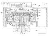
- FIG. 1is a sectional side view of a plasma processing chamber having an electrostatic chuck assembly according to one embodiment of the present invention.
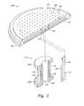
- FIG. 2is an exploded perspective sectional view of a chuck body according to one embodiment of the present invention.
- FIG. 3is an exploded perspective sectional view of an electrostatic chuck assembly according to one embodiment of the present invention.
- Embodiments of the present inventionrelate to apparatus and methods for supporting a substrate in a processing chamber operating at elevated temperatures. More particularly, embodiments of the present invention provide an electrostatic chuck assembly for operating at elevated temperatures.
- One embodimentprovides a dielectric chuck body having a dielectric disk and a shaft extending from the dielectric disk.
- the shaftis hollow and has a central opening providing passage for connectors to an RF, a DC or an RF/DC combined electrode and/or heating elements embedded in dielectric disk.
- the shaftalso has one or more channels formed through a sidewall along the axial direction. The one or more channels may be used to provide integrated passages for cooling fluids and/or substrate sensor passages or connections. By using the channels formed in the sidewall of the shaft, embodiments of the present invention avoid sealing cooling fluid passages using o-rings which may not withstand high temperature.
- Embodiments of the present inventionfurther provide a cooling base attached to the dielectric chuck body at a distal end of the shaft to provide temperature control to the dielectric chuck body. No clamping is applied between the cooling base and an edge of the supporting disk of the dielectric chuck body.
- Embodiments of the present inventioninclude enabling an electrostatic chuck to perform at high temperatures.
- electrostatic chuck according to embodiments of the present inventionmay operate in an etching environment maintained at a temperature of up to about 400 degrees Celsius.
- Certain embodiments of the present inventionalso provide a two zone temperature control to achieve a target substrate temperature profile.
- Embodiments of the present inventionalso eliminate metal contamination associated with from metal clamping structures used in traditional electrostatic chucks to secure a dielectric chuck body to a cooling base.
- Embodiments of the present inventionalso provide integrated passages for cooling fluids and/or leads to sensors and eliminate usages of sealing o-rings which may not withstand high temperatures.
- Certain embodiments of the present inventionalso provide a wafer temperature monitoring (WTM) system that improves process quality.
- WTMwafer temperature monitoring
- FIG. 1is a sectional side view of a plasma processing chamber 100 having an electrostatic chuck assembly 120 according to one embodiment of the present invention.
- the plasma processing chamber 100includes a chamber housing assembly 101 defining an inner volume 110 .
- the chamber housing assembly 101includes chamber walls 104 , a chamber lid 102 disposed over the chamber walls 104 , and a chamber bottom 105 .
- the electrostatic chuck assembly 120is disposed in the inner volume 110 of the housing assembly 101 to support a substrate 112 thereon.
- the electrostatic chuck assembly 120may be attached to housing assembly 101 via an interfacing plate 108 , and may extend outside of the plasma processing chamber 100 via a bottom opening 106 formed through the chamber bottom 105 .
- a liner 130may be disposed inside the chamber sidewalls 104 surrounding a portion of the inner volume 110 above the electrostatic chuck assembly 120 to create a processing volume 132 above the substrate 112 .
- a slit valve opening 104 ais formed through the chamber walls 104 and a corresponding opening 130 a formed through the liner 130 to allow passage of substrates and substrate transfer mechanism used to place and retrieve substrates from the electrostatic chuck assembly 120 .
- a gas injection assembly 134is disposed over the electrostatic chuck assembly 120 to provide one or more processing gas from a gas source 136 to the processing volume 132 .
- a vacuum pump 140may be coupled to the inner volume 110 to pump processing gases out of the plasma processing chamber 100 via a plenum 138 disposed in an edge region of the processing volume 132 .
- an antenna assembly 142may be disposed outside the chamber lid 102 to facilitate plasma processing.
- the antenna assembly 142may be coupled to a radio-frequency (RF) plasma power source 146 through a matching network 144 .
- RFradio-frequency
- the antenna assembly 142is energized with RF power provided by the power source 146 to ignite a plasma of processing gases within the processing volume 132 and to maintain the plasma.
- the electrostatic chuck assembly 120includes a dielectric chuck body 121 configured to secure and support the substrate 112 and a cooling base 126 configured to provide temperature control of the dielectric chuck body 121 .
- the dielectric chuck body 121includes a substrate supporting plate 122 having a top surface 123 for supporting the substrate 112 and a back surface 125 opposing the top surface 123 .
- the dielectric chuck body 121also includes a shaft 124 extending from the back surface 125 of the substrate supporting plate 122 .
- the shaft 124is fixedly attached to the substrate support plate 122 at a first end 124 a and attached to the cooling base 126 at a second end 124 b .
- the dielectric chuck body 121 and the cooling base 126do not have additional fixed connections, such as clamping elements around the substrate support plate 122 , other than the connection at the second end 124 b of the shaft 124 .
- This configurationallows the dielectric chuck body 121 and the cooling base 126 to move relative to one another under thermal expansion, therefore, avoids thermal stress between the dielectric chuck body 121 and the cooling base 126 . Since the dielectric chuck body 121 and the cooling base 126 are connected at a center of the dielectric chuck body 121 , the dielectric chuck body 121 is free to expand radially in all directions relative the cooling base 126 . The contact between the second end 124 b and the cooling base 126 provides primary heat exchange between the cooling base 126 and the dielectric chuck body 121 .
- the substrate supporting plate 122is generally substantially planar and shaped to support the entire substrate 112 .
- the substrate supporting plate 122may be circular, rectangular or other suitable shape for supporting a circular substrate, a rectangular substrates, or substrates of other shapes.
- the substrate supporting plate 122may be fabricated from ceramic, such as aluminum nitride, aluminum oxide, or doped ceramics such as alumina doped with titanium nitride or chromium nitride, doped aluminum oxide, doped boron-nitride and the like. In one embodiment, the substrate supporting plate 122 may be formed from about 95 % pure aluminum nitride to enhance thermal conductivity of the substrate supporting plate 122 .
- the dielectric chuck body 121further includes an electrode 156 embedded in the substrate supporting plate 122 .
- the electrode 156may be a thin metal plate or a metal mesh.
- the electrode 156may be large enough to encompass substantially the entire area of the substrate 112 .
- the electrode 156may be coupled to a power source, such as a DC voltage source, to produce electrostatic chucking force to attract and secure the substrate 112 on the top surface 123 .
- the electrode 156may also be coupled to a RF power source for generating capactively coupled plasma in a processing chamber 100 .
- the dielectric chuck body 121further includes one or more heating elements 160 embedded in the substrate supporting plate 122 .
- the one or more heating elements 160may be resistive heaters.
- the one or more heating elements 160enables the substrate supporting plate 122 to heat the substrate 112 to a desired temperature, for example, a temperature between about 200 to about 400 degree Celsius.
- the one or more heating elements 160may form two independently controlled temperature zones.
- three or more lift pins 116may be movable through the substrate supporting plate 122 , the cooling base 126 , and the interface plate 108 by a lift pin drive 114 .
- the three or more lift pins 116are configured to pick up the substrate 112 from the substrate supporting plate 122 .
- the shaft 124may be fabricated from ceramics, such as aluminum nitride, aluminum oxide, or doped ceramics such as alumina doped with titanium nitride or chromium nitride, doped aluminum oxide, doped boron-nitride and the like. In one embodiment, the shaft 124 may be formed from about 95 % pure aluminum nitride to enhance thermal conductivity. In one embodiment, the shaft 124 and the substrate supporting plate 122 may be fabricated from the same material. The shaft 124 may be joined to the substrate supporting plate 122 by bonding to form an integrated dielectric chuck body. In one embodiment, the shaft 124 may be joined to the substrate supporting plate 122 by explosion bonding. In one embodiment, the shaft 124 may be joined to the substrate supporting plate 124 by diffusion bonding. Alternatively, the shaft 124 may be joined to the substrate supporting plate 124 brazing, or other suitable bonding methods that can form an integrated dielectric chuck body.
- ceramicssuch as aluminum nitride, aluminum oxide, or do
- the shaft 124is hollow having a sidewall 170 defining a central opening 172 extending from the first end 124 a to the second end 124 b .
- the central opening 172is configured to provide a passage for connectors 157 , 159 , 161 that connect the electrode 156 to a power source 158 and the one or more heating elements 160 to a heating power source 162 .
- one or more channels 174 , 176may be formed through the sidewall 170 of the shaft 124 .
- the one or more channels 174 , 176may extend from the first end 124 a to the second end 124 b .
- the one or more channels 174 , 176connect and become integrated with channels 178 , 180 in the substrate supporting plate 122 forming one or more passage for cooling fluid and/or sensor leads.
- the nature of the bond between the shaft 124 and the substrate support plate 122provides a leek-free interface between the channels 174 , 176 and the channels 178 , 180 .
- the channel 176may be a blind hole for receiving a sensor, such as a thermal couple, without exposing the sensor to the processing environment in the processing volume 132 .
- the channel 174connects the channel 178 in the substrate supporting plate 122 to a cooling fluid source 182 .
- the channel 178opens at the top surface 123 of the substrate supporting plate 122 .
- the channel 174 and the channel 178form a passage for supporting a cooling fluid, such as helium, from the cooling fluid source 182 to a backside of the substrate 112 to control substrate temperature.
- the channel 176 in the shaft 124connects to the channel 180 in the substrate supporting plate 122 to form a passage for a sensor 186 .
- the sensor 186may be positioned in the substrate supporting plate 122 proximate the top surface 123 .
- the sensor 186may be connected to a controller 184 through a sensor lead 185 disposed in the channel 176 and the channel 180 .
- the sensormay be positioned at the end 124 b of the shaft 124 .
- the sensor 186is a temperature sensor configured to measure the temperature of the substrate 112 disposed over the substrate support plate 122 .
- the shaft 124 and the substrate supporting plate 122are bonded together to make a leak-tight seal.
- the shaft 124 and the substrate supporting plate 122may be explosion bonded.
- the channels 174 , 176connect to the channel 178 , 180 by integration without using any O-rings which may not be able to stand high temperatures.
- the integrated channels 174 , 176 , 178 , 180enable the electrostatic chuck body 120 to operate at temperatures above most O-ring's service temperature limits.
- the cooling base 126is disposed under the dielectric chuck body 120 in the inner volume 110 .
- the cooling base 126is mounted on an interface plate 108 disposed on the chamber bottom 105 .
- the cooling base 126may have a body 188 having a substantially planar top surface 187 and a cylindrical extension 190 opposing the top surface 187 .
- a recess 189is formed from the top surface 187 for receiving the shaft 124 of the dielectric chuck body 120 and extends into the cylindrical extension 190 .
- the cylindrical extension 190may extend through the bottom opening 106 of the chamber bottom 105 .
- a plurality of cooling channels 194are formed in the cooling base 126 for circulation of a cooling fluid.
- the cooling channels 194may be in fluid communication with a cooling fluid source 196 .
- the cooling base 126may be fabricated from a thermally conductive material, and in one embodiment, is fabricated from a metal, such as aluminum or stainless steel, and in one embodiment.
- the facing surfaces of the cooling base 126 and the shaft 124are clamped together, for example using a plurality of screws 133 .
- a washer 131may be disposed between the shaft 124 and the cooling base 126 to ensure solid contact and good heat exchange between the cooling base 126 and the shaft 124 .
- the second end 124 b of the shaft 124sits on a bottom surface 192 of the recess 189 of the cooling base 126 while the top surface 187 of the cooling base 126 and the back surface 125 of the substrate supporting plate 122 do not make direct contact. Similarly, a sidewall 191 of the recess 189 also does not contact the shaft 124 directly.
- a gap 127is formed between the cooling base 126 and the dielectric chuck body 120 to allow relative thermal expansion.
- a secondary thermal contact between the cooling base 126 and the dielectric chuck body 120may be established by a contact element 128 and a springing element 129 disposed between the cooling base 126 and the dielectric chuck body 120 .
- a groove 135may be formed in the top surface 187 of the cooling base 126 .
- the groove 135may be placed and shaped corresponding to an edge region of the substrate supporting plate 122 to provide temperature control the edge region of the substrate supporting plate 122 .
- the springing element 129is disposed in the groove 135 .
- the contact element 128is disposed over the springing element 129 .
- the springing element 129pushes the contact element 128 against the back surface 125 of the substrate supporting plate 122 .
- the springing element 129 and contact element 128provide a conductive path between the cooling base 126 and the substrate supporting plate 122 without applying any lateral and vertical motion restraints between the substrate supporting plate 122 and the cooling base 126 .
- the contact element 128 and the springing element 129may be formed from thermal conductive materials.
- the contact element 128is formed from ceramic material, such as aluminum oxide or aluminum nitride.
- the springing element 129may be formed from metal, such as aluminum or stainless steel.
- an edge ring assembly 150may be disposed around the gap 127 to isolate the gaps 127 and 189 from the processing volume 132 .
- the edge ring assembly 150may include a lower ring 151 and an upper ring 152 .
- the lower ring 151may be disposed over the cooling base 126 surrounding the gap 127 .
- the upper ring 152may be supported by an edge of the substrate supporting plate 122 and suspended above the lower ring 151 .
- a gap 150 amay is formed between a lower surface 152 a of the upper ring 152 and an upper surface 151 a of the lower ring 151 to allow thermal expansion of the cooling base 126 and the dielectric chuck body 120 .
- the lower surface 152 a of the upper ring 152 and the upper surface 151 a of the lower ring 151may have interleaving features, such as a rib and a groove, that form a labyrinth in the gap 150 a .
- the labyrinth in the gap 150 aprovides separation between the gap 127 and the processing volume 132 .
- the labyrinthsubstantially prevents processing gas in the processing volume 132 from entering the gaps 127 , 189 thus reducing undesirable contamination.
- the lower ring 151 and upper ring 152may be formed from material compatible to the processing chemistry.
- the lower ring 151 and upper ring 152may be fabricated from ceramic or quartz.
- a shadow ring 154may be disposed over the substrate supporting plate 122 around an edge region to cover areas outside the substrate 112 and prevent the covered areas from exposure to the processing chemistry.
- FIG. 2is an exploded perspective sectional view of the dielectric chuck body 120 .
- the channels 174 , 176 in the sidewall 170form integrated passages for cooling fluid and/or sensor leads. Even though two channels 174 , 176 are shown in FIG. 2 , more channels may be formed to accommodate additional needs.
- the shaft 126has a flange 202 that provides increased surface area for enhancing heat exchange with the cooling base 126 .
- FIG. 3is an exploded perspective sectional view of the electrostatic chuck assembly including the cooling base 126 and the dielectric chuck body 120 , illustrating the components discussed above.
Landscapes
- Engineering & Computer Science (AREA)
- Physics & Mathematics (AREA)
- Condensed Matter Physics & Semiconductors (AREA)
- General Physics & Mathematics (AREA)
- Manufacturing & Machinery (AREA)
- Computer Hardware Design (AREA)
- Microelectronics & Electronic Packaging (AREA)
- Power Engineering (AREA)
- Container, Conveyance, Adherence, Positioning, Of Wafer (AREA)
Abstract
Description
- This application claims benefit of U.S. Provisional Patent Applications Ser. No. 61/638,857 filed Apr. 26, 2012, Ser. No. 61/639,228 filed Apr. 27, 2012 and Serial No. 61/639,719 filed Apr. 27, 2012. The aforementioned patent applications are herein incorporated by reference.
- 1. Field
- Embodiments of the present invention generally relate to apparatus and methods for processing substrate at high temperature. Particularly, embodiments of the present invention relate to apparatus and methods for supporting a substrate in a processing chamber operating at high temperatures.
- 2. Description of the Related Art
- Electrostatic chucks are commonly used in supporting and securing a substrate in a processing chamber. An electrostatic chuck generally has a non-conductive body, such as a ceramic body, having an embedded DC electrode for generating chucking force. One or more heating element may be included in the substrate support to provide heating during processing. An RF electrode may be embedded inside a non-conductive body. The RF electrode delivers bias power to generate plasma while the DC electrode generates chucking force for securing a substrate thereon. A heater may be embedded in the non-conductive body to provide heating. A cooling base may be attached to non-conductive body to cool the non-conductive body. The heater and the cooling base work together to control the temperature of the electrostatic chuck and the substrate supported thereon.
- Existing electrostatic chucks generally have metal clamping devices to secure the non-conductive body and the cooling base and use organic O-rings to provide sealing. However, the metal clamping devices and organic O-rings cannot function properly at elevated temperatures, such as at a temperature higher than 350° C. At 350° C., the operating temperature exceeds the performance limits for high temperature organic O-Rings. At elevated temperatures, metal clamping devices constrain thermal expansion of the non-conductive body and the cooling base. Additionally, metal clamping devices, generally made from refractory metal such as titanium, will also introduce metal contamination under processing chemistry.
- Therefore, there is a need for electrostatic chuck for operating at elevated temperatures.
- Embodiments of the present invention relate to apparatus and methods for supporting a substrate in a processing chamber operating at high temperatures. Particularly, embodiments of the present invention provide electrostatic chucks for operating at elevated temperatures.
- One embodiment of the present invention provides a dielectric chuck body for an electrostatic chuck. The dielectric chuck body includes a substrate supporting plate having a top surface for receiving a substrate and a back surface opposing the top surface, an electrode embedded in the substrate supporting plate and configured to generate chucking force for securing the substrate on the top surface and/or to generate plasma for processing, and a shaft having a first end attached to the back surface of the substrate supporting plate and a second end opposing the first end. The second end is configured to contact a cooling base and provide temperature control to the substrate supporting plate. The shaft is hollow having a sidewall enclosing a central opening, and two or more channels formed through the sidewall and extending from the first end to the second end.
- Another embodiment of the present invention provides an electrostatic chuck assembly. The electrostatic chuck assembly includes a dielectric chuck body according to one embodiment of the present invention, and a cooling base configured to provide temperature control to the dielectric chuck body. The cooling base and the dielectric chuck body are coupled together at the second end of the shaft of the dielectric chuck body. A gap is formed between the back surface of the substrate supporting plate and a top surface of the cooling base.
- Another embodiment of the present invention provides an apparatus for processing a substrate. The apparatus includes a chamber housing assembly defining an inner volume, an electrostatic chuck assembly according to one embodiment of the present invention disposed in the inner volume and configured to secure and support a substrate in the inner volume during processing. The apparatus further includes a gas injection assembly configured to deliver one or more processing gas over the substrate disposed on the electrostatic chuck assembly.
- So that the manner in which the above recited features of the present invention can be understood in detail, a more particular description of the invention, briefly summarized above, may be had by reference to embodiments, some of which are illustrated in the appended drawings. It is to be noted, however, that the appended drawings illustrate only typical embodiments of this invention and are therefore not to be considered limiting of its scope, for the invention may admit to other equally effective embodiments.
FIG. 1 is a sectional side view of a plasma processing chamber having an electrostatic chuck assembly according to one embodiment of the present invention.FIG. 2 is an exploded perspective sectional view of a chuck body according to one embodiment of the present invention.FIG. 3 is an exploded perspective sectional view of an electrostatic chuck assembly according to one embodiment of the present invention.- To facilitate understanding, identical reference numerals have been used, where possible, to designate identical elements that are common to the figures. It is contemplated that elements disclosed in one embodiment may be beneficially utilized on other embodiments without specific recitation.
- Embodiments of the present invention relate to apparatus and methods for supporting a substrate in a processing chamber operating at elevated temperatures. More particularly, embodiments of the present invention provide an electrostatic chuck assembly for operating at elevated temperatures. One embodiment provides a dielectric chuck body having a dielectric disk and a shaft extending from the dielectric disk. The shaft is hollow and has a central opening providing passage for connectors to an RF, a DC or an RF/DC combined electrode and/or heating elements embedded in dielectric disk. The shaft also has one or more channels formed through a sidewall along the axial direction. The one or more channels may be used to provide integrated passages for cooling fluids and/or substrate sensor passages or connections. By using the channels formed in the sidewall of the shaft, embodiments of the present invention avoid sealing cooling fluid passages using o-rings which may not withstand high temperature.
- Embodiments of the present invention further provide a cooling base attached to the dielectric chuck body at a distal end of the shaft to provide temperature control to the dielectric chuck body. No clamping is applied between the cooling base and an edge of the supporting disk of the dielectric chuck body. By attaching the cooling base and the dielectric chuck body at the distal end of the shaft and avoiding clamping to the edge of the supporting disk, embodiments of the present invention eliminate restrains to thermal expansion in the structure, and also reduce particle generation caused by conventional clamping structures.
- Embodiments of the present invention include enabling an electrostatic chuck to perform at high temperatures. For example, electrostatic chuck according to embodiments of the present invention may operate in an etching environment maintained at a temperature of up to about 400 degrees Celsius. Certain embodiments of the present invention also provide a two zone temperature control to achieve a target substrate temperature profile. Embodiments of the present invention also eliminate metal contamination associated with from metal clamping structures used in traditional electrostatic chucks to secure a dielectric chuck body to a cooling base. Embodiments of the present invention also provide integrated passages for cooling fluids and/or leads to sensors and eliminate usages of sealing o-rings which may not withstand high temperatures. Certain embodiments of the present invention also provide a wafer temperature monitoring (WTM) system that improves process quality.
FIG. 1 is a sectional side view of aplasma processing chamber 100 having anelectrostatic chuck assembly 120 according to one embodiment of the present invention. Theplasma processing chamber 100 includes a chamber housing assembly101 defining aninner volume 110. The chamber housing assembly101 includeschamber walls 104, achamber lid 102 disposed over thechamber walls 104, and achamber bottom 105.- The
electrostatic chuck assembly 120 is disposed in theinner volume 110 of the housing assembly101 to support asubstrate 112 thereon. Theelectrostatic chuck assembly 120 may be attached to housing assembly101 via aninterfacing plate 108, and may extend outside of theplasma processing chamber 100 via abottom opening 106 formed through thechamber bottom 105. - A liner130 may be disposed inside the chamber sidewalls104 surrounding a portion of the
inner volume 110 above theelectrostatic chuck assembly 120 to create aprocessing volume 132 above thesubstrate 112. A slit valve opening104ais formed through thechamber walls 104 and acorresponding opening 130aformed through the liner130 to allow passage of substrates and substrate transfer mechanism used to place and retrieve substrates from theelectrostatic chuck assembly 120. - A
gas injection assembly 134 is disposed over theelectrostatic chuck assembly 120 to provide one or more processing gas from agas source 136 to theprocessing volume 132. Avacuum pump 140 may be coupled to theinner volume 110 to pump processing gases out of theplasma processing chamber 100 via aplenum 138 disposed in an edge region of theprocessing volume 132. - In one embodiment, an
antenna assembly 142 may be disposed outside thechamber lid 102 to facilitate plasma processing. Theantenna assembly 142 may be coupled to a radio-frequency (RF)plasma power source 146 through amatching network 144. During processing, theantenna assembly 142 is energized with RF power provided by thepower source 146 to ignite a plasma of processing gases within theprocessing volume 132 and to maintain the plasma. - The
electrostatic chuck assembly 120 includes adielectric chuck body 121 configured to secure and support thesubstrate 112 and acooling base 126 configured to provide temperature control of thedielectric chuck body 121. Thedielectric chuck body 121 includes asubstrate supporting plate 122 having atop surface 123 for supporting thesubstrate 112 and aback surface 125 opposing thetop surface 123. Thedielectric chuck body 121 also includes ashaft 124 extending from theback surface 125 of thesubstrate supporting plate 122. Theshaft 124 is fixedly attached to thesubstrate support plate 122 at afirst end 124aand attached to thecooling base 126 at asecond end 124b. According to one embodiment of the present invention, thedielectric chuck body 121 and thecooling base 126 do not have additional fixed connections, such as clamping elements around thesubstrate support plate 122, other than the connection at thesecond end 124bof theshaft 124. This configuration allows thedielectric chuck body 121 and thecooling base 126 to move relative to one another under thermal expansion, therefore, avoids thermal stress between thedielectric chuck body 121 and thecooling base 126. Since thedielectric chuck body 121 and thecooling base 126 are connected at a center of thedielectric chuck body 121, thedielectric chuck body 121 is free to expand radially in all directions relative thecooling base 126. The contact between thesecond end 124band thecooling base 126 provides primary heat exchange between the coolingbase 126 and thedielectric chuck body 121. - The
substrate supporting plate 122 is generally substantially planar and shaped to support theentire substrate 112. Thesubstrate supporting plate 122 may be circular, rectangular or other suitable shape for supporting a circular substrate, a rectangular substrates, or substrates of other shapes. Thesubstrate supporting plate 122 may be fabricated from ceramic, such as aluminum nitride, aluminum oxide, or doped ceramics such as alumina doped with titanium nitride or chromium nitride, doped aluminum oxide, doped boron-nitride and the like. In one embodiment, thesubstrate supporting plate 122 may be formed from about95% pure aluminum nitride to enhance thermal conductivity of thesubstrate supporting plate 122. - The
dielectric chuck body 121 further includes anelectrode 156 embedded in thesubstrate supporting plate 122. Theelectrode 156 may be a thin metal plate or a metal mesh. Theelectrode 156 may be large enough to encompass substantially the entire area of thesubstrate 112. Theelectrode 156 may be coupled to a power source, such as a DC voltage source, to produce electrostatic chucking force to attract and secure thesubstrate 112 on thetop surface 123. Optionally, theelectrode 156 may also be coupled to a RF power source for generating capactively coupled plasma in aprocessing chamber 100. - In one embodiment, the
dielectric chuck body 121 further includes one ormore heating elements 160 embedded in thesubstrate supporting plate 122. The one ormore heating elements 160 may be resistive heaters. The one ormore heating elements 160 enables thesubstrate supporting plate 122 to heat thesubstrate 112 to a desired temperature, for example, a temperature between about 200 to about 400 degree Celsius. In one embodiment, the one ormore heating elements 160 may form two independently controlled temperature zones. - According to one embodiment of the present invention, three or more lift pins116 may be movable through the
substrate supporting plate 122, thecooling base 126, and theinterface plate 108 by alift pin drive 114. The three or more lift pins116 are configured to pick up thesubstrate 112 from thesubstrate supporting plate 122. - The
shaft 124 may be fabricated from ceramics, such as aluminum nitride, aluminum oxide, or doped ceramics such as alumina doped with titanium nitride or chromium nitride, doped aluminum oxide, doped boron-nitride and the like. In one embodiment, theshaft 124 may be formed from about95% pure aluminum nitride to enhance thermal conductivity. In one embodiment, theshaft 124 and thesubstrate supporting plate 122 may be fabricated from the same material. Theshaft 124 may be joined to thesubstrate supporting plate 122 by bonding to form an integrated dielectric chuck body. In one embodiment, theshaft 124 may be joined to thesubstrate supporting plate 122 by explosion bonding. In one embodiment, theshaft 124 may be joined to thesubstrate supporting plate 124 by diffusion bonding. Alternatively, theshaft 124 may be joined to thesubstrate supporting plate 124 brazing, or other suitable bonding methods that can form an integrated dielectric chuck body. - The
shaft 124 is hollow having asidewall 170 defining acentral opening 172 extending from thefirst end 124ato thesecond end 124b. In one embodiment, thecentral opening 172 is configured to provide a passage forconnectors electrode 156 to apower source 158 and the one ormore heating elements 160 to aheating power source 162. - According to one embodiment of the present invention, one or
more channels sidewall 170 of theshaft 124. The one ormore channels first end 124ato thesecond end 124b. When theshaft 124 is joined to thesubstrate supporting plate 122, the one ormore channels channels substrate supporting plate 122 forming one or more passage for cooling fluid and/or sensor leads. The nature of the bond between theshaft 124 and thesubstrate support plate 122 provides a leek-free interface between thechannels channels channel 176 may be a blind hole for receiving a sensor, such as a thermal couple, without exposing the sensor to the processing environment in theprocessing volume 132. - As shown in
FIG. 1 , thechannel 174 connects thechannel 178 in thesubstrate supporting plate 122 to a coolingfluid source 182. Thechannel 178 opens at thetop surface 123 of thesubstrate supporting plate 122. Thechannel 174 and thechannel 178 form a passage for supporting a cooling fluid, such as helium, from the coolingfluid source 182 to a backside of thesubstrate 112 to control substrate temperature. Thechannel 176 in theshaft 124 connects to thechannel 180 in thesubstrate supporting plate 122 to form a passage for asensor 186. Thesensor 186 may be positioned in thesubstrate supporting plate 122 proximate thetop surface 123. Thesensor 186 may be connected to acontroller 184 through asensor lead 185 disposed in thechannel 176 and thechannel 180. Optionally, the sensor may be positioned at theend 124bof theshaft 124. In one embodiment, thesensor 186 is a temperature sensor configured to measure the temperature of thesubstrate 112 disposed over thesubstrate support plate 122. - The
shaft 124 and thesubstrate supporting plate 122 are bonded together to make a leak-tight seal. In one embodiment, theshaft 124 and thesubstrate supporting plate 122 may be explosion bonded. Thechannels channel integrated channels electrostatic chuck body 120 to operate at temperatures above most O-ring's service temperature limits. - The
cooling base 126 is disposed under thedielectric chuck body 120 in theinner volume 110. In one embodiment, thecooling base 126 is mounted on aninterface plate 108 disposed on thechamber bottom 105. Thecooling base 126 may have abody 188 having a substantially planartop surface 187 and acylindrical extension 190 opposing thetop surface 187. Arecess 189 is formed from thetop surface 187 for receiving theshaft 124 of thedielectric chuck body 120 and extends into thecylindrical extension 190. Thecylindrical extension 190 may extend through thebottom opening 106 of thechamber bottom 105. - A plurality of cooling
channels 194 are formed in thecooling base 126 for circulation of a cooling fluid. The coolingchannels 194 may be in fluid communication with a coolingfluid source 196. Thecooling base 126 may be fabricated from a thermally conductive material, and in one embodiment, is fabricated from a metal, such as aluminum or stainless steel, and in one embodiment. - The facing surfaces of the
cooling base 126 and theshaft 124 are clamped together, for example using a plurality ofscrews 133. In one embodiment, awasher 131 may be disposed between theshaft 124 and thecooling base 126 to ensure solid contact and good heat exchange between the coolingbase 126 and theshaft 124. - When assembled, the
second end 124bof theshaft 124 sits on abottom surface 192 of therecess 189 of thecooling base 126 while thetop surface 187 of thecooling base 126 and theback surface 125 of thesubstrate supporting plate 122 do not make direct contact. Similarly, asidewall 191 of therecess 189 also does not contact theshaft 124 directly. Agap 127 is formed between the coolingbase 126 and thedielectric chuck body 120 to allow relative thermal expansion. - Optionally, a secondary thermal contact between the cooling
base 126 and thedielectric chuck body 120 may be established by acontact element 128 and aspringing element 129 disposed between the coolingbase 126 and thedielectric chuck body 120. In one embodiment, agroove 135 may be formed in thetop surface 187 of thecooling base 126. Thegroove 135 may be placed and shaped corresponding to an edge region of thesubstrate supporting plate 122 to provide temperature control the edge region of thesubstrate supporting plate 122. The springingelement 129 is disposed in thegroove 135. Thecontact element 128 is disposed over the springingelement 129. The springingelement 129 pushes thecontact element 128 against theback surface 125 of thesubstrate supporting plate 122. The springingelement 129 andcontact element 128 provide a conductive path between the coolingbase 126 and thesubstrate supporting plate 122 without applying any lateral and vertical motion restraints between thesubstrate supporting plate 122 and thecooling base 126. Thecontact element 128 and the springingelement 129 may be formed from thermal conductive materials. In one embodiment, thecontact element 128 is formed from ceramic material, such as aluminum oxide or aluminum nitride. The springingelement 129 may be formed from metal, such as aluminum or stainless steel. - According to one embodiment of the present invention, an
edge ring assembly 150 may be disposed around thegap 127 to isolate thegaps processing volume 132. Theedge ring assembly 150 may include alower ring 151 and anupper ring 152. Thelower ring 151 may be disposed over thecooling base 126 surrounding thegap 127. Theupper ring 152 may be supported by an edge of thesubstrate supporting plate 122 and suspended above thelower ring 151. Agap 150amay is formed between alower surface 152aof theupper ring 152 and anupper surface 151aof thelower ring 151 to allow thermal expansion of thecooling base 126 and thedielectric chuck body 120. Thelower surface 152aof theupper ring 152 and theupper surface 151aof thelower ring 151 may have interleaving features, such as a rib and a groove, that form a labyrinth in thegap 150a. The labyrinth in thegap 150aprovides separation between thegap 127 and theprocessing volume 132. The labyrinth substantially prevents processing gas in theprocessing volume 132 from entering thegaps lower ring 151 andupper ring 152 may be formed from material compatible to the processing chemistry. In one embodiment, thelower ring 151 andupper ring 152 may be fabricated from ceramic or quartz. Ashadow ring 154 may be disposed over thesubstrate supporting plate 122 around an edge region to cover areas outside thesubstrate 112 and prevent the covered areas from exposure to the processing chemistry. FIG. 2 is an exploded perspective sectional view of thedielectric chuck body 120. Thechannels sidewall 170 form integrated passages for cooling fluid and/or sensor leads. Even though twochannels FIG. 2 , more channels may be formed to accommodate additional needs. Theshaft 126 has aflange 202 that provides increased surface area for enhancing heat exchange with thecooling base 126.FIG. 3 is an exploded perspective sectional view of the electrostatic chuck assembly including thecooling base 126 and thedielectric chuck body 120, illustrating the components discussed above.- While the foregoing is directed to embodiments of the present invention, other and further embodiments of the invention may be devised without departing from the basic scope thereof, and the scope thereof is determined by the claims that follow.
Claims (20)
1. A dielectric chuck body for an electrostatic chuck, comprising:
a substrate supporting plate having a top surface for receiving a substrate and a back surface opposing the top surface;
an electrode embedded in the substrate supporting plate; and
a shaft having a first end attached to the back surface of the substrate supporting plate and a second end opposing the first end, wherein the second end is configured to contact a cooling base and provide temperature control to the substrate supporting plate, the shaft being hollow and having a sidewall enclosing a central opening, and two or more channels formed through the sidewall and extending from the first end to the second end.
2. The dielectric chuck body ofclaim 1 , further comprising one or more heating elements embedded in the substrate supporting plate and configured to heat the substrate disposed on the top surface.
3. The dielectric chuck body ofclaim 2 , wherein the one or more heating elements form two or more independent heating zones.
4. The dielectric chuck body ofclaim 2 , further comprising connectors disposed in the central opening of the shaft, wherein the connectors are coupled to the one or more heating elements and the electrode and are adapted to connect the one or more heating elements and the electrode to external power sources.
5. The dielectric body ofclaim 1 , wherein the substrate support plate and the shaft are bonded together to form leak-tight channels therebetween.
6. The dielectric chuck body ofclaim 1 , wherein the substrate supporting plate has a cooling channel configured to provide a cooling fluid to the substrate.
7. The dielectric chuck body ofclaim 6 , further comprising a temperature sensor disposed in the substrate supporting plate, wherein the temperature sensor is configured to measure temperature of the substrate disposed on the substrate supporting plate, and a sensor lead passes through one of the two or more channels formed through the sidewall of the shaft.
8. The dielectric chuck body ofclaim 5 , wherein the substrate supporting plate and the shaft are fabricated from ceramic.
9. The dielectric chuck body ofclaim 1 , wherein the shaft has a flange formed on the second end for effective heat exchange with the cooling base.
10. An electrostatic chuck assembly, comprising:
a dielectric chuck body ofclaim 1 ; and
a cooling base configured to provide temperature control to the dielectric chuck body, wherein the cooling base and the dielectric chuck body are coupled together at the second end of the shaft of the dielectric chuck body, and a gap is formed between the back surface of the substrate supporting plate and a top surface of the cooling base.
11. The electrostatic chuck assembly ofclaim 10 , wherein the cooling base comprises a body having a recess formed therein, and a bottom surface of the recess contacts the shaft of the dielectric chuck body.
12. The electrostatic chuck assembly ofclaim 11 , further comprising:
a contact element; and
a springing element, wherein the contact element and the springing element span the gap between the cooling base and the substrate supporting plate, and provides a conductive path between the cooling base and the back surface of the substrate supporting plate.
13. The electrostatic chuck assembly ofclaim 12 , the substrate support plate and the shaft are bonded together to form leak-tight channels therebetween.
14. The electrostatic chuck assembly ofclaim 12 , wherein the substrate supporting plate has a cooling channel configured to provide a cooling fluid to the substrate.
15. The electrostatic chuck assembly ofclaim 10 , wherein the substrate supporting plate and the shaft are fabricated from ceramic.
16. The electrostatic chuck assembly ofclaim 15 , wherein the edge ring assembly comprises:
a lower ring disposed over the cooling base; and
an upper ring supported by the substrate supporting plate, wherein the upper ring is suspended over the lower ring, a lower surface of the upper ring faces an upper surface of the lower ring, interleaving features are formed in the lower surface of the upper ring and the upper surface of the lower ring, and the interleaving features form a labyrinth between the lower ring and the upper ring.
17. The electrostatic chuck assembly ofclaim 10 , further comprising a conductive structure disposed between the cooling base and the shaft of the dielectric chuck body.
18. An apparatus for processing a substrate, comprising:
a chamber housing assembly defining an inner volume;
an electrostatic chuck assembly ofclaim 10 disposed in the inner volume and configured to secure and support a substrate in the inner volume during processing; and
a gas injection assembly configured to deliver one or more processing gas over the substrate disposed on the electrostatic chuck assembly.
19. The apparatus ofclaim 18 , further comprising a liner disposed inside the chamber housing assembly surrounding a portion of the inner volume above the electrostatic chuck assembly to create a processing volume above the substrate.
20. The apparatus ofclaim 18 , further comprising a shadow ring disposed over an edge region of the substrate supporting plate to protect the edge region of the substrate supporting plate.
Priority Applications (6)
| Application Number | Priority Date | Filing Date | Title |
|---|---|---|---|
| US13/793,512US9948214B2 (en) | 2012-04-26 | 2013-03-11 | High temperature electrostatic chuck with real-time heat zone regulating capability |
| PCT/US2013/034380WO2013162820A1 (en) | 2012-04-26 | 2013-03-28 | High temperature electrostatic chuck with real-time heat zone regulating capability |
| CN201380016503.1ACN104205321B (en) | 2012-04-26 | 2013-03-28 | High temperature electrostatic fixture with real-time hot-zone regulating power |
| JP2015508985AJP2015517224A (en) | 2012-04-26 | 2013-03-28 | High-temperature electrostatic chuck with real-time heating zone adjustment function |
| KR1020147031651AKR102151001B1 (en) | 2012-04-26 | 2013-03-28 | High temperature electrostatic chuck with real-time heat zone regulating capability |
| TW102114621ATW201351559A (en) | 2012-04-26 | 2013-04-24 | High temperature electrostatic chuck with real-time heat zone regulating capability |
Applications Claiming Priority (4)
| Application Number | Priority Date | Filing Date | Title |
|---|---|---|---|
| US201261638857P | 2012-04-26 | 2012-04-26 | |
| US201261639228P | 2012-04-27 | 2012-04-27 | |
| US201261639719P | 2012-04-27 | 2012-04-27 | |
| US13/793,512US9948214B2 (en) | 2012-04-26 | 2013-03-11 | High temperature electrostatic chuck with real-time heat zone regulating capability |
Publications (2)
| Publication Number | Publication Date |
|---|---|
| US20130284374A1true US20130284374A1 (en) | 2013-10-31 |
| US9948214B2 US9948214B2 (en) | 2018-04-17 |
Family
ID=49476309
Family Applications (1)
| Application Number | Title | Priority Date | Filing Date |
|---|---|---|---|
| US13/793,512Active2035-03-07US9948214B2 (en) | 2012-04-26 | 2013-03-11 | High temperature electrostatic chuck with real-time heat zone regulating capability |
Country Status (6)
| Country | Link |
|---|---|
| US (1) | US9948214B2 (en) |
| JP (1) | JP2015517224A (en) |
| KR (1) | KR102151001B1 (en) |
| CN (1) | CN104205321B (en) |
| TW (1) | TW201351559A (en) |
| WO (1) | WO2013162820A1 (en) |
Cited By (118)
| Publication number | Priority date | Publication date | Assignee | Title |
|---|---|---|---|---|
| US20140302256A1 (en)* | 2013-03-27 | 2014-10-09 | Applied Materials, Inc. | High impedance rf filter for heater with impedance tuning device |
| WO2015105647A1 (en)* | 2014-01-07 | 2015-07-16 | Applied Materials, Inc. | Pecvd ceramic heater with wide range of operating temperatures |
| US20150371881A1 (en)* | 2013-03-14 | 2015-12-24 | Applied Materials, Inc. | Temperature measurement in multi-zone heater |
| CN105552014A (en)* | 2014-10-28 | 2016-05-04 | 北京北方微电子基地设备工艺研究中心有限责任公司 | Support device and plasma etching equipment |
| US9355922B2 (en) | 2014-10-14 | 2016-05-31 | Applied Materials, Inc. | Systems and methods for internal surface conditioning in plasma processing equipment |
| US20160225651A1 (en)* | 2015-02-03 | 2016-08-04 | Applied Materials, Inc. | High temperature chuck for plasma processing systems |
| WO2016197083A1 (en)* | 2015-06-05 | 2016-12-08 | Watlow Electric Manufacturing Company | High thermal conductivity wafer support pedestal device |
| US9576809B2 (en) | 2013-11-04 | 2017-02-21 | Applied Materials, Inc. | Etch suppression with germanium |
| US9613822B2 (en) | 2014-09-25 | 2017-04-04 | Applied Materials, Inc. | Oxide etch selectivity enhancement |
| US9659753B2 (en) | 2014-08-07 | 2017-05-23 | Applied Materials, Inc. | Grooved insulator to reduce leakage current |
| US9691645B2 (en) | 2015-08-06 | 2017-06-27 | Applied Materials, Inc. | Bolted wafer chuck thermal management systems and methods for wafer processing systems |
| US9704723B2 (en) | 2013-03-15 | 2017-07-11 | Applied Materials, Inc. | Processing systems and methods for halide scavenging |
| US9711366B2 (en) | 2013-11-12 | 2017-07-18 | Applied Materials, Inc. | Selective etch for metal-containing materials |
| US9721789B1 (en) | 2016-10-04 | 2017-08-01 | Applied Materials, Inc. | Saving ion-damaged spacers |
| US20170229326A1 (en)* | 2015-02-03 | 2017-08-10 | Applied Materials, Inc. | Low temperature chuck for plasma processing systems |
| US9741593B2 (en) | 2015-08-06 | 2017-08-22 | Applied Materials, Inc. | Thermal management systems and methods for wafer processing systems |
| US9754800B2 (en) | 2010-05-27 | 2017-09-05 | Applied Materials, Inc. | Selective etch for silicon films |
| US9768034B1 (en) | 2016-11-11 | 2017-09-19 | Applied Materials, Inc. | Removal methods for high aspect ratio structures |
| US9773648B2 (en) | 2013-08-30 | 2017-09-26 | Applied Materials, Inc. | Dual discharge modes operation for remote plasma |
| US9773695B2 (en) | 2014-07-31 | 2017-09-26 | Applied Materials, Inc. | Integrated bit-line airgap formation and gate stack post clean |
| US9837249B2 (en) | 2014-03-20 | 2017-12-05 | Applied Materials, Inc. | Radial waveguide systems and methods for post-match control of microwaves |
| US9842744B2 (en) | 2011-03-14 | 2017-12-12 | Applied Materials, Inc. | Methods for etch of SiN films |
| US9865484B1 (en) | 2016-06-29 | 2018-01-09 | Applied Materials, Inc. | Selective etch using material modification and RF pulsing |
| US9881805B2 (en) | 2015-03-02 | 2018-01-30 | Applied Materials, Inc. | Silicon selective removal |
| US9885117B2 (en) | 2014-03-31 | 2018-02-06 | Applied Materials, Inc. | Conditioned semiconductor system parts |
| US9934942B1 (en) | 2016-10-04 | 2018-04-03 | Applied Materials, Inc. | Chamber with flow-through source |
| US9948214B2 (en)* | 2012-04-26 | 2018-04-17 | Applied Materials, Inc. | High temperature electrostatic chuck with real-time heat zone regulating capability |
| US9947549B1 (en) | 2016-10-10 | 2018-04-17 | Applied Materials, Inc. | Cobalt-containing material removal |
| US9966240B2 (en) | 2014-10-14 | 2018-05-08 | Applied Materials, Inc. | Systems and methods for internal surface conditioning assessment in plasma processing equipment |
| US9978564B2 (en) | 2012-09-21 | 2018-05-22 | Applied Materials, Inc. | Chemical control features in wafer process equipment |
| US10026621B2 (en) | 2016-11-14 | 2018-07-17 | Applied Materials, Inc. | SiN spacer profile patterning |
| US10032606B2 (en) | 2012-08-02 | 2018-07-24 | Applied Materials, Inc. | Semiconductor processing with DC assisted RF power for improved control |
| US10043684B1 (en) | 2017-02-06 | 2018-08-07 | Applied Materials, Inc. | Self-limiting atomic thermal etching systems and methods |
| US10043674B1 (en) | 2017-08-04 | 2018-08-07 | Applied Materials, Inc. | Germanium etching systems and methods |
| US10049891B1 (en) | 2017-05-31 | 2018-08-14 | Applied Materials, Inc. | Selective in situ cobalt residue removal |
| US10062585B2 (en) | 2016-10-04 | 2018-08-28 | Applied Materials, Inc. | Oxygen compatible plasma source |
| US10062579B2 (en) | 2016-10-07 | 2018-08-28 | Applied Materials, Inc. | Selective SiN lateral recess |
| US10062578B2 (en) | 2011-03-14 | 2018-08-28 | Applied Materials, Inc. | Methods for etch of metal and metal-oxide films |
| US10062587B2 (en) | 2012-07-18 | 2018-08-28 | Applied Materials, Inc. | Pedestal with multi-zone temperature control and multiple purge capabilities |
| US10062575B2 (en) | 2016-09-09 | 2018-08-28 | Applied Materials, Inc. | Poly directional etch by oxidation |
| US10128086B1 (en) | 2017-10-24 | 2018-11-13 | Applied Materials, Inc. | Silicon pretreatment for nitride removal |
| US10163696B2 (en) | 2016-11-11 | 2018-12-25 | Applied Materials, Inc. | Selective cobalt removal for bottom up gapfill |
| US10170336B1 (en) | 2017-08-04 | 2019-01-01 | Applied Materials, Inc. | Methods for anisotropic control of selective silicon removal |
| US10224210B2 (en) | 2014-12-09 | 2019-03-05 | Applied Materials, Inc. | Plasma processing system with direct outlet toroidal plasma source |
| US10242908B2 (en) | 2016-11-14 | 2019-03-26 | Applied Materials, Inc. | Airgap formation with damage-free copper |
| US10256112B1 (en) | 2017-12-08 | 2019-04-09 | Applied Materials, Inc. | Selective tungsten removal |
| US10256079B2 (en) | 2013-02-08 | 2019-04-09 | Applied Materials, Inc. | Semiconductor processing systems having multiple plasma configurations |
| US10283324B1 (en) | 2017-10-24 | 2019-05-07 | Applied Materials, Inc. | Oxygen treatment for nitride etching |
| US10283321B2 (en) | 2011-01-18 | 2019-05-07 | Applied Materials, Inc. | Semiconductor processing system and methods using capacitively coupled plasma |
| US10297458B2 (en) | 2017-08-07 | 2019-05-21 | Applied Materials, Inc. | Process window widening using coated parts in plasma etch processes |
| US10319649B2 (en) | 2017-04-11 | 2019-06-11 | Applied Materials, Inc. | Optical emission spectroscopy (OES) for remote plasma monitoring |
| US10319739B2 (en) | 2017-02-08 | 2019-06-11 | Applied Materials, Inc. | Accommodating imperfectly aligned memory holes |
| US10319600B1 (en) | 2018-03-12 | 2019-06-11 | Applied Materials, Inc. | Thermal silicon etch |
| US10354889B2 (en) | 2017-07-17 | 2019-07-16 | Applied Materials, Inc. | Non-halogen etching of silicon-containing materials |
| US20190237353A1 (en)* | 2018-02-01 | 2019-08-01 | Lam Research Corporation | Electrostatic chucking pedestal with substrate backside purging and thermal sinking |
| US10403507B2 (en) | 2017-02-03 | 2019-09-03 | Applied Materials, Inc. | Shaped etch profile with oxidation |
| CN110265323A (en)* | 2019-05-31 | 2019-09-20 | 沈阳拓荆科技有限公司 | Wafer heated seats with crosspoint array |
| US10424485B2 (en) | 2013-03-01 | 2019-09-24 | Applied Materials, Inc. | Enhanced etching processes using remote plasma sources |
| US10424464B2 (en) | 2015-08-07 | 2019-09-24 | Applied Materials, Inc. | Oxide etch selectivity systems and methods |
| US10431429B2 (en) | 2017-02-03 | 2019-10-01 | Applied Materials, Inc. | Systems and methods for radial and azimuthal control of plasma uniformity |
| WO2019190797A1 (en)* | 2018-03-27 | 2019-10-03 | Lam Research Corporation | Connector for substrate support with embedded temperature sensors |
| US10465294B2 (en) | 2014-05-28 | 2019-11-05 | Applied Materials, Inc. | Oxide and metal removal |
| US10468267B2 (en) | 2017-05-31 | 2019-11-05 | Applied Materials, Inc. | Water-free etching methods |
| US10490406B2 (en) | 2018-04-10 | 2019-11-26 | Appled Materials, Inc. | Systems and methods for material breakthrough |
| US10497573B2 (en) | 2018-03-13 | 2019-12-03 | Applied Materials, Inc. | Selective atomic layer etching of semiconductor materials |
| US10504700B2 (en) | 2015-08-27 | 2019-12-10 | Applied Materials, Inc. | Plasma etching systems and methods with secondary plasma injection |
| US10504754B2 (en) | 2016-05-19 | 2019-12-10 | Applied Materials, Inc. | Systems and methods for improved semiconductor etching and component protection |
| US10522371B2 (en) | 2016-05-19 | 2019-12-31 | Applied Materials, Inc. | Systems and methods for improved semiconductor etching and component protection |
| US10541184B2 (en) | 2017-07-11 | 2020-01-21 | Applied Materials, Inc. | Optical emission spectroscopic techniques for monitoring etching |
| US10541246B2 (en) | 2017-06-26 | 2020-01-21 | Applied Materials, Inc. | 3D flash memory cells which discourage cross-cell electrical tunneling |
| US10546729B2 (en) | 2016-10-04 | 2020-01-28 | Applied Materials, Inc. | Dual-channel showerhead with improved profile |
| WO2020027919A1 (en)* | 2018-07-30 | 2020-02-06 | Nordson Corporation | Systems for workpiece processing with plasma |
| US10566206B2 (en) | 2016-12-27 | 2020-02-18 | Applied Materials, Inc. | Systems and methods for anisotropic material breakthrough |
| WO2020036613A1 (en)* | 2018-08-13 | 2020-02-20 | Lam Research Corporation | Replaceable and/or collapsible edge ring assemblies for plasma sheath tuning incorporating edge ring positioning and centering features |
| US10573496B2 (en) | 2014-12-09 | 2020-02-25 | Applied Materials, Inc. | Direct outlet toroidal plasma source |
| US10573527B2 (en) | 2018-04-06 | 2020-02-25 | Applied Materials, Inc. | Gas-phase selective etching systems and methods |
| US10593560B2 (en) | 2018-03-01 | 2020-03-17 | Applied Materials, Inc. | Magnetic induction plasma source for semiconductor processes and equipment |
| US10615047B2 (en) | 2018-02-28 | 2020-04-07 | Applied Materials, Inc. | Systems and methods to form airgaps |
| US10629473B2 (en) | 2016-09-09 | 2020-04-21 | Applied Materials, Inc. | Footing removal for nitride spacer |
| US10672642B2 (en) | 2018-07-24 | 2020-06-02 | Applied Materials, Inc. | Systems and methods for pedestal configuration |
| US10679870B2 (en) | 2018-02-15 | 2020-06-09 | Applied Materials, Inc. | Semiconductor processing chamber multistage mixing apparatus |
| US10699879B2 (en) | 2018-04-17 | 2020-06-30 | Applied Materials, Inc. | Two piece electrode assembly with gap for plasma control |
| US10727080B2 (en) | 2017-07-07 | 2020-07-28 | Applied Materials, Inc. | Tantalum-containing material removal |
| US10755941B2 (en) | 2018-07-06 | 2020-08-25 | Applied Materials, Inc. | Self-limiting selective etching systems and methods |
| US20200312696A1 (en)* | 2018-03-26 | 2020-10-01 | Ngk Insulators, Ltd. | Electrostatic-chuck heater |
| US10840117B2 (en) | 2016-09-12 | 2020-11-17 | Ngk Spark Plug Co., Ltd. | Holding apparatus |
| US10854426B2 (en) | 2018-01-08 | 2020-12-01 | Applied Materials, Inc. | Metal recess for semiconductor structures |
| US10872778B2 (en) | 2018-07-06 | 2020-12-22 | Applied Materials, Inc. | Systems and methods utilizing solid-phase etchants |
| US10886137B2 (en) | 2018-04-30 | 2021-01-05 | Applied Materials, Inc. | Selective nitride removal |
| US10892198B2 (en) | 2018-09-14 | 2021-01-12 | Applied Materials, Inc. | Systems and methods for improved performance in semiconductor processing |
| US10903054B2 (en) | 2017-12-19 | 2021-01-26 | Applied Materials, Inc. | Multi-zone gas distribution systems and methods |
| US10920320B2 (en) | 2017-06-16 | 2021-02-16 | Applied Materials, Inc. | Plasma health determination in semiconductor substrate processing reactors |
| US10920319B2 (en) | 2019-01-11 | 2021-02-16 | Applied Materials, Inc. | Ceramic showerheads with conductive electrodes |
| US10943834B2 (en) | 2017-03-13 | 2021-03-09 | Applied Materials, Inc. | Replacement contact process |
| US10964512B2 (en) | 2018-02-15 | 2021-03-30 | Applied Materials, Inc. | Semiconductor processing chamber multistage mixing apparatus and methods |
| US11049755B2 (en) | 2018-09-14 | 2021-06-29 | Applied Materials, Inc. | Semiconductor substrate supports with embedded RF shield |
| US11062887B2 (en) | 2018-09-17 | 2021-07-13 | Applied Materials, Inc. | High temperature RF heater pedestals |
| US11121002B2 (en) | 2018-10-24 | 2021-09-14 | Applied Materials, Inc. | Systems and methods for etching metals and metal derivatives |
| US11239061B2 (en) | 2014-11-26 | 2022-02-01 | Applied Materials, Inc. | Methods and systems to enhance process uniformity |
| US11257693B2 (en) | 2015-01-09 | 2022-02-22 | Applied Materials, Inc. | Methods and systems to improve pedestal temperature control |
| US20220055450A1 (en)* | 2020-08-19 | 2022-02-24 | Lexmark International, Inc. | Cabin heater |
| US11276559B2 (en) | 2017-05-17 | 2022-03-15 | Applied Materials, Inc. | Semiconductor processing chamber for multiple precursor flow |
| US11276590B2 (en) | 2017-05-17 | 2022-03-15 | Applied Materials, Inc. | Multi-zone semiconductor substrate supports |
| US11289355B2 (en) | 2017-06-02 | 2022-03-29 | Lam Research Corporation | Electrostatic chuck for use in semiconductor processing |
| WO2022076144A1 (en)* | 2020-10-06 | 2022-04-14 | Applied Materials, Inc. | Shadow ring kit for plasma etch wafer singulation process |
| US11328909B2 (en) | 2017-12-22 | 2022-05-10 | Applied Materials, Inc. | Chamber conditioning and removal processes |
| US11417534B2 (en) | 2018-09-21 | 2022-08-16 | Applied Materials, Inc. | Selective material removal |
| US11424096B2 (en)* | 2019-11-05 | 2022-08-23 | Applied Materials, Inc. | Temperature controlled secondary electrode for ion control at substrate edge |
| US11437242B2 (en) | 2018-11-27 | 2022-09-06 | Applied Materials, Inc. | Selective removal of silicon-containing materials |
| US20220312553A1 (en)* | 2021-03-26 | 2022-09-29 | Applied Materials, Inc. | Heater assembly with purge gap control and temperature uniformity for batch processing chambers |
| US20230073711A1 (en)* | 2021-09-08 | 2023-03-09 | Tokyo Electron Limited | Substrate support assembly and plasma processing apparatus |
| US20230147452A1 (en)* | 2019-05-24 | 2023-05-11 | Applied Materials, Inc. | Substrate pedestal for improved substrate processing |
| US11682560B2 (en) | 2018-10-11 | 2023-06-20 | Applied Materials, Inc. | Systems and methods for hafnium-containing film removal |
| US11721527B2 (en) | 2019-01-07 | 2023-08-08 | Applied Materials, Inc. | Processing chamber mixing systems |
| US12027410B2 (en) | 2015-01-16 | 2024-07-02 | Lam Research Corporation | Edge ring arrangement with moveable edge rings |
| US12183554B2 (en) | 2017-11-21 | 2024-12-31 | Lam Research Corporation | Bottom and middle edge rings |
| US12340979B2 (en) | 2017-05-17 | 2025-06-24 | Applied Materials, Inc. | Semiconductor processing chamber for improved precursor flow |
| US12444579B2 (en) | 2020-03-23 | 2025-10-14 | Lam Research Corporation | Mid-ring erosion compensation in substrate processing systems |
Families Citing this family (19)
| Publication number | Priority date | Publication date | Assignee | Title |
|---|---|---|---|---|
| US10497606B2 (en)* | 2015-02-09 | 2019-12-03 | Applied Materials, Inc. | Dual-zone heater for plasma processing |
| KR102540912B1 (en) | 2015-08-27 | 2023-06-08 | 스미토모 오사카 세멘토 가부시키가이샤 | electrostatic chuck device |
| US10184183B2 (en)* | 2016-06-21 | 2019-01-22 | Applied Materials, Inc. | Substrate temperature monitoring |
| CN106229284A (en)* | 2016-07-19 | 2016-12-14 | 武汉新芯集成电路制造有限公司 | A kind of dot matrix temperature control Electrostatic Absorption dish |
| JP6704821B2 (en)* | 2016-09-12 | 2020-06-03 | 日本特殊陶業株式会社 | Holding device |
| US11469084B2 (en) | 2017-09-05 | 2022-10-11 | Lam Research Corporation | High temperature RF connection with integral thermal choke |
| US11990360B2 (en) | 2018-01-31 | 2024-05-21 | Lam Research Corporation | Electrostatic chuck (ESC) pedestal voltage isolation |
| JP6522180B1 (en)* | 2018-02-08 | 2019-05-29 | Sppテクノロジーズ株式会社 | Substrate mounting table, plasma processing apparatus provided with the same, and plasma processing method |
| US11086233B2 (en) | 2018-03-20 | 2021-08-10 | Lam Research Corporation | Protective coating for electrostatic chucks |
| CN108650722B (en)* | 2018-04-28 | 2021-11-12 | 拓荆科技股份有限公司 | Heating plate for improving radio frequency conduction capability and sealing effect |
| US11183368B2 (en) | 2018-08-02 | 2021-11-23 | Lam Research Corporation | RF tuning systems including tuning circuits having impedances for setting and adjusting parameters of electrodes in electrostatic chucks |
| JP7112915B2 (en)* | 2018-09-07 | 2022-08-04 | 東京エレクトロン株式会社 | temperature control system |
| US11564292B2 (en)* | 2019-09-27 | 2023-01-24 | Applied Materials, Inc. | Monolithic modular microwave source with integrated temperature control |
| US11133213B2 (en)* | 2019-11-05 | 2021-09-28 | Applied Materials, Inc. | Deflectable platen and associated method |
| CN111968901B (en)* | 2020-08-25 | 2022-08-16 | 北京北方华创微电子装备有限公司 | Semiconductor reaction chamber and semiconductor processing equipment |
| JP7674059B2 (en)* | 2021-01-22 | 2025-05-09 | 東京エレクトロン株式会社 | Mounting table structure, substrate processing apparatus, and method for controlling substrate processing apparatus |
| US12062565B2 (en) | 2021-06-29 | 2024-08-13 | Asm Ip Holding B.V. | Electrostatic chuck, assembly including the electrostatic chuck, and method of controlling temperature of the electrostatic chuck |
| JP7729764B2 (en)* | 2021-10-06 | 2025-08-26 | 日本特殊陶業株式会社 | Substrate holding member |
| JP7733531B2 (en)* | 2021-10-08 | 2025-09-03 | 日本特殊陶業株式会社 | Substrate holding member |
Citations (11)
| Publication number | Priority date | Publication date | Assignee | Title |
|---|---|---|---|---|
| US4869801A (en)* | 1988-02-05 | 1989-09-26 | Leybold Aktiengesellschaft | Apparatus for mounting workpieces |
| US5063031A (en)* | 1989-08-24 | 1991-11-05 | Kabushiki Kaisha Toshiba | Apparatus for growing vapor phase layer on semiconductor substrate |
| US6160244A (en)* | 1998-05-29 | 2000-12-12 | Ngk Insulators, Ltd. | Susceptors |
| US6313443B1 (en)* | 1999-04-20 | 2001-11-06 | Steag Cvd Systems, Ltd. | Apparatus for processing material at controlled temperatures |
| US20020050246A1 (en)* | 2000-06-09 | 2002-05-02 | Applied Materials, Inc. | Full area temperature controlled electrostatic chuck and method of fabricating same |
| US20030213436A1 (en)* | 2002-05-18 | 2003-11-20 | Hyung-Jin Kwon | Batch type atomic layer deposition apparatus |
| US20090236315A1 (en)* | 2008-03-21 | 2009-09-24 | Applied Materials, Inc. | Shielded lid heater assembly |
| US20090274590A1 (en)* | 2008-05-05 | 2009-11-05 | Applied Materials, Inc. | Plasma reactor electrostatic chuck having a coaxial rf feed and multizone ac heater power transmission through the coaxial feed |
| US20100018648A1 (en)* | 2008-07-23 | 2010-01-28 | Applied Marterials, Inc. | Workpiece support for a plasma reactor with controlled apportionment of rf power to a process kit ring |
| US20100229794A1 (en)* | 2009-02-26 | 2010-09-16 | Kenji Iso | Vapor phase epitaxy apparatus of group iii nitride semiconductor |
| US9150981B2 (en)* | 2009-07-15 | 2015-10-06 | Nuflare Technology, Inc. | Manufacturing apparatus and method for semiconductor device |
Family Cites Families (8)
| Publication number | Priority date | Publication date | Assignee | Title |
|---|---|---|---|---|
| US6377437B1 (en)* | 1999-12-22 | 2002-04-23 | Lam Research Corporation | High temperature electrostatic chuck |
| JP4644943B2 (en) | 2001-01-23 | 2011-03-09 | 東京エレクトロン株式会社 | Processing equipment |
| JPWO2007018139A1 (en) | 2005-08-10 | 2009-02-19 | 株式会社日立国際電気 | Semiconductor device manufacturing method and substrate processing apparatus |
| US20100101728A1 (en) | 2007-03-29 | 2010-04-29 | Tokyo Electron Limited | Plasma process apparatus |
| JP4450106B1 (en)* | 2008-03-11 | 2010-04-14 | 東京エレクトロン株式会社 | Mounting table structure and processing device |
| KR101681897B1 (en) | 2009-08-07 | 2016-12-05 | 어플라이드 머티어리얼스, 인코포레이티드 | Dual temperature heater |
| JP5835985B2 (en) | 2010-09-16 | 2015-12-24 | 東京エレクトロン株式会社 | Plasma processing apparatus and plasma processing method |
| US9948214B2 (en)* | 2012-04-26 | 2018-04-17 | Applied Materials, Inc. | High temperature electrostatic chuck with real-time heat zone regulating capability |
- 2013
- 2013-03-11USUS13/793,512patent/US9948214B2/enactiveActive
- 2013-03-28CNCN201380016503.1Apatent/CN104205321B/enactiveActive
- 2013-03-28KRKR1020147031651Apatent/KR102151001B1/enactiveActive
- 2013-03-28WOPCT/US2013/034380patent/WO2013162820A1/enactiveApplication Filing
- 2013-03-28JPJP2015508985Apatent/JP2015517224A/enactivePending
- 2013-04-24TWTW102114621Apatent/TW201351559A/enunknown
Patent Citations (12)
| Publication number | Priority date | Publication date | Assignee | Title |
|---|---|---|---|---|
| US4869801A (en)* | 1988-02-05 | 1989-09-26 | Leybold Aktiengesellschaft | Apparatus for mounting workpieces |
| US5063031A (en)* | 1989-08-24 | 1991-11-05 | Kabushiki Kaisha Toshiba | Apparatus for growing vapor phase layer on semiconductor substrate |
| US6160244A (en)* | 1998-05-29 | 2000-12-12 | Ngk Insulators, Ltd. | Susceptors |
| US6313443B1 (en)* | 1999-04-20 | 2001-11-06 | Steag Cvd Systems, Ltd. | Apparatus for processing material at controlled temperatures |
| US20020050246A1 (en)* | 2000-06-09 | 2002-05-02 | Applied Materials, Inc. | Full area temperature controlled electrostatic chuck and method of fabricating same |
| US6853533B2 (en)* | 2000-06-09 | 2005-02-08 | Applied Materials, Inc. | Full area temperature controlled electrostatic chuck and method of fabricating same |
| US20030213436A1 (en)* | 2002-05-18 | 2003-11-20 | Hyung-Jin Kwon | Batch type atomic layer deposition apparatus |
| US20090236315A1 (en)* | 2008-03-21 | 2009-09-24 | Applied Materials, Inc. | Shielded lid heater assembly |
| US20090274590A1 (en)* | 2008-05-05 | 2009-11-05 | Applied Materials, Inc. | Plasma reactor electrostatic chuck having a coaxial rf feed and multizone ac heater power transmission through the coaxial feed |
| US20100018648A1 (en)* | 2008-07-23 | 2010-01-28 | Applied Marterials, Inc. | Workpiece support for a plasma reactor with controlled apportionment of rf power to a process kit ring |
| US20100229794A1 (en)* | 2009-02-26 | 2010-09-16 | Kenji Iso | Vapor phase epitaxy apparatus of group iii nitride semiconductor |
| US9150981B2 (en)* | 2009-07-15 | 2015-10-06 | Nuflare Technology, Inc. | Manufacturing apparatus and method for semiconductor device |
Cited By (174)
| Publication number | Priority date | Publication date | Assignee | Title |
|---|---|---|---|---|
| US9754800B2 (en) | 2010-05-27 | 2017-09-05 | Applied Materials, Inc. | Selective etch for silicon films |
| US10283321B2 (en) | 2011-01-18 | 2019-05-07 | Applied Materials, Inc. | Semiconductor processing system and methods using capacitively coupled plasma |
| US9842744B2 (en) | 2011-03-14 | 2017-12-12 | Applied Materials, Inc. | Methods for etch of SiN films |
| US10062578B2 (en) | 2011-03-14 | 2018-08-28 | Applied Materials, Inc. | Methods for etch of metal and metal-oxide films |
| US9948214B2 (en)* | 2012-04-26 | 2018-04-17 | Applied Materials, Inc. | High temperature electrostatic chuck with real-time heat zone regulating capability |
| US10062587B2 (en) | 2012-07-18 | 2018-08-28 | Applied Materials, Inc. | Pedestal with multi-zone temperature control and multiple purge capabilities |
| US10032606B2 (en) | 2012-08-02 | 2018-07-24 | Applied Materials, Inc. | Semiconductor processing with DC assisted RF power for improved control |
| US10354843B2 (en) | 2012-09-21 | 2019-07-16 | Applied Materials, Inc. | Chemical control features in wafer process equipment |
| US9978564B2 (en) | 2012-09-21 | 2018-05-22 | Applied Materials, Inc. | Chemical control features in wafer process equipment |
| US11264213B2 (en) | 2012-09-21 | 2022-03-01 | Applied Materials, Inc. | Chemical control features in wafer process equipment |
| US10256079B2 (en) | 2013-02-08 | 2019-04-09 | Applied Materials, Inc. | Semiconductor processing systems having multiple plasma configurations |
| US11024486B2 (en) | 2013-02-08 | 2021-06-01 | Applied Materials, Inc. | Semiconductor processing systems having multiple plasma configurations |
| US10424485B2 (en) | 2013-03-01 | 2019-09-24 | Applied Materials, Inc. | Enhanced etching processes using remote plasma sources |
| US20150371881A1 (en)* | 2013-03-14 | 2015-12-24 | Applied Materials, Inc. | Temperature measurement in multi-zone heater |
| US10720349B2 (en) | 2013-03-14 | 2020-07-21 | Applied Materials, Inc. | Temperature measurement in multi-zone heater |
| US10153185B2 (en)* | 2013-03-14 | 2018-12-11 | Applied Materials, Inc. | Substrate temperature measurement in multi-zone heater |
| US9704723B2 (en) | 2013-03-15 | 2017-07-11 | Applied Materials, Inc. | Processing systems and methods for halide scavenging |
| US20140302256A1 (en)* | 2013-03-27 | 2014-10-09 | Applied Materials, Inc. | High impedance rf filter for heater with impedance tuning device |
| US10450653B2 (en) | 2013-03-27 | 2019-10-22 | Applied Materials, Inc. | High impedance RF filter for heater with impedance tuning device |
| US10125422B2 (en)* | 2013-03-27 | 2018-11-13 | Applied Materials, Inc. | High impedance RF filter for heater with impedance tuning device |
| US9773648B2 (en) | 2013-08-30 | 2017-09-26 | Applied Materials, Inc. | Dual discharge modes operation for remote plasma |
| US9576809B2 (en) | 2013-11-04 | 2017-02-21 | Applied Materials, Inc. | Etch suppression with germanium |
| US9711366B2 (en) | 2013-11-12 | 2017-07-18 | Applied Materials, Inc. | Selective etch for metal-containing materials |
| WO2015105647A1 (en)* | 2014-01-07 | 2015-07-16 | Applied Materials, Inc. | Pecvd ceramic heater with wide range of operating temperatures |
| US9837249B2 (en) | 2014-03-20 | 2017-12-05 | Applied Materials, Inc. | Radial waveguide systems and methods for post-match control of microwaves |
| US9885117B2 (en) | 2014-03-31 | 2018-02-06 | Applied Materials, Inc. | Conditioned semiconductor system parts |
| US9903020B2 (en) | 2014-03-31 | 2018-02-27 | Applied Materials, Inc. | Generation of compact alumina passivation layers on aluminum plasma equipment components |
| US10465294B2 (en) | 2014-05-28 | 2019-11-05 | Applied Materials, Inc. | Oxide and metal removal |
| US9773695B2 (en) | 2014-07-31 | 2017-09-26 | Applied Materials, Inc. | Integrated bit-line airgap formation and gate stack post clean |
| US9659753B2 (en) | 2014-08-07 | 2017-05-23 | Applied Materials, Inc. | Grooved insulator to reduce leakage current |
| US9613822B2 (en) | 2014-09-25 | 2017-04-04 | Applied Materials, Inc. | Oxide etch selectivity enhancement |
| US9837284B2 (en) | 2014-09-25 | 2017-12-05 | Applied Materials, Inc. | Oxide etch selectivity enhancement |
| US10707061B2 (en) | 2014-10-14 | 2020-07-07 | Applied Materials, Inc. | Systems and methods for internal surface conditioning in plasma processing equipment |
| US10796922B2 (en) | 2014-10-14 | 2020-10-06 | Applied Materials, Inc. | Systems and methods for internal surface conditioning assessment in plasma processing equipment |
| US10593523B2 (en) | 2014-10-14 | 2020-03-17 | Applied Materials, Inc. | Systems and methods for internal surface conditioning in plasma processing equipment |
| US9966240B2 (en) | 2014-10-14 | 2018-05-08 | Applied Materials, Inc. | Systems and methods for internal surface conditioning assessment in plasma processing equipment |
| US10490418B2 (en) | 2014-10-14 | 2019-11-26 | Applied Materials, Inc. | Systems and methods for internal surface conditioning assessment in plasma processing equipment |
| US9355922B2 (en) | 2014-10-14 | 2016-05-31 | Applied Materials, Inc. | Systems and methods for internal surface conditioning in plasma processing equipment |
| CN105552014A (en)* | 2014-10-28 | 2016-05-04 | 北京北方微电子基地设备工艺研究中心有限责任公司 | Support device and plasma etching equipment |
| US11637002B2 (en) | 2014-11-26 | 2023-04-25 | Applied Materials, Inc. | Methods and systems to enhance process uniformity |
| US11239061B2 (en) | 2014-11-26 | 2022-02-01 | Applied Materials, Inc. | Methods and systems to enhance process uniformity |
| US10573496B2 (en) | 2014-12-09 | 2020-02-25 | Applied Materials, Inc. | Direct outlet toroidal plasma source |
| US10224210B2 (en) | 2014-12-09 | 2019-03-05 | Applied Materials, Inc. | Plasma processing system with direct outlet toroidal plasma source |
| US11257693B2 (en) | 2015-01-09 | 2022-02-22 | Applied Materials, Inc. | Methods and systems to improve pedestal temperature control |
| US12027410B2 (en) | 2015-01-16 | 2024-07-02 | Lam Research Corporation | Edge ring arrangement with moveable edge rings |
| US10468285B2 (en) | 2015-02-03 | 2019-11-05 | Applied Materials, Inc. | High temperature chuck for plasma processing systems |
| US20160225651A1 (en)* | 2015-02-03 | 2016-08-04 | Applied Materials, Inc. | High temperature chuck for plasma processing systems |
| US12009228B2 (en) | 2015-02-03 | 2024-06-11 | Applied Materials, Inc. | Low temperature chuck for plasma processing systems |
| US9728437B2 (en)* | 2015-02-03 | 2017-08-08 | Applied Materials, Inc. | High temperature chuck for plasma processing systems |
| US11594428B2 (en)* | 2015-02-03 | 2023-02-28 | Applied Materials, Inc. | Low temperature chuck for plasma processing systems |
| US20170229326A1 (en)* | 2015-02-03 | 2017-08-10 | Applied Materials, Inc. | Low temperature chuck for plasma processing systems |
| US9881805B2 (en) | 2015-03-02 | 2018-01-30 | Applied Materials, Inc. | Silicon selective removal |
| WO2016197083A1 (en)* | 2015-06-05 | 2016-12-08 | Watlow Electric Manufacturing Company | High thermal conductivity wafer support pedestal device |
| US10147620B2 (en) | 2015-08-06 | 2018-12-04 | Applied Materials, Inc. | Bolted wafer chuck thermal management systems and methods for wafer processing systems |
| US10607867B2 (en) | 2015-08-06 | 2020-03-31 | Applied Materials, Inc. | Bolted wafer chuck thermal management systems and methods for wafer processing systems |
| US10468276B2 (en) | 2015-08-06 | 2019-11-05 | Applied Materials, Inc. | Thermal management systems and methods for wafer processing systems |
| US9691645B2 (en) | 2015-08-06 | 2017-06-27 | Applied Materials, Inc. | Bolted wafer chuck thermal management systems and methods for wafer processing systems |
| US9741593B2 (en) | 2015-08-06 | 2017-08-22 | Applied Materials, Inc. | Thermal management systems and methods for wafer processing systems |
| US11158527B2 (en) | 2015-08-06 | 2021-10-26 | Applied Materials, Inc. | Thermal management systems and methods for wafer processing systems |
| US10424463B2 (en) | 2015-08-07 | 2019-09-24 | Applied Materials, Inc. | Oxide etch selectivity systems and methods |
| US10424464B2 (en) | 2015-08-07 | 2019-09-24 | Applied Materials, Inc. | Oxide etch selectivity systems and methods |
| US11476093B2 (en) | 2015-08-27 | 2022-10-18 | Applied Materials, Inc. | Plasma etching systems and methods with secondary plasma injection |
| US10504700B2 (en) | 2015-08-27 | 2019-12-10 | Applied Materials, Inc. | Plasma etching systems and methods with secondary plasma injection |
| US11735441B2 (en) | 2016-05-19 | 2023-08-22 | Applied Materials, Inc. | Systems and methods for improved semiconductor etching and component protection |
| US10504754B2 (en) | 2016-05-19 | 2019-12-10 | Applied Materials, Inc. | Systems and methods for improved semiconductor etching and component protection |
| US10522371B2 (en) | 2016-05-19 | 2019-12-31 | Applied Materials, Inc. | Systems and methods for improved semiconductor etching and component protection |
| US12057329B2 (en) | 2016-06-29 | 2024-08-06 | Applied Materials, Inc. | Selective etch using material modification and RF pulsing |
| US9865484B1 (en) | 2016-06-29 | 2018-01-09 | Applied Materials, Inc. | Selective etch using material modification and RF pulsing |
| US10629473B2 (en) | 2016-09-09 | 2020-04-21 | Applied Materials, Inc. | Footing removal for nitride spacer |
| US10062575B2 (en) | 2016-09-09 | 2018-08-28 | Applied Materials, Inc. | Poly directional etch by oxidation |
| US10840117B2 (en) | 2016-09-12 | 2020-11-17 | Ngk Spark Plug Co., Ltd. | Holding apparatus |
| US10541113B2 (en) | 2016-10-04 | 2020-01-21 | Applied Materials, Inc. | Chamber with flow-through source |
| US9721789B1 (en) | 2016-10-04 | 2017-08-01 | Applied Materials, Inc. | Saving ion-damaged spacers |
| US10062585B2 (en) | 2016-10-04 | 2018-08-28 | Applied Materials, Inc. | Oxygen compatible plasma source |
| US11049698B2 (en) | 2016-10-04 | 2021-06-29 | Applied Materials, Inc. | Dual-channel showerhead with improved profile |
| US10546729B2 (en) | 2016-10-04 | 2020-01-28 | Applied Materials, Inc. | Dual-channel showerhead with improved profile |
| US10224180B2 (en) | 2016-10-04 | 2019-03-05 | Applied Materials, Inc. | Chamber with flow-through source |
| US9934942B1 (en) | 2016-10-04 | 2018-04-03 | Applied Materials, Inc. | Chamber with flow-through source |
| US10062579B2 (en) | 2016-10-07 | 2018-08-28 | Applied Materials, Inc. | Selective SiN lateral recess |
| US10319603B2 (en) | 2016-10-07 | 2019-06-11 | Applied Materials, Inc. | Selective SiN lateral recess |
| US9947549B1 (en) | 2016-10-10 | 2018-04-17 | Applied Materials, Inc. | Cobalt-containing material removal |
| US10770346B2 (en) | 2016-11-11 | 2020-09-08 | Applied Materials, Inc. | Selective cobalt removal for bottom up gapfill |
| US9768034B1 (en) | 2016-11-11 | 2017-09-19 | Applied Materials, Inc. | Removal methods for high aspect ratio structures |
| US10186428B2 (en) | 2016-11-11 | 2019-01-22 | Applied Materials, Inc. | Removal methods for high aspect ratio structures |
| US10163696B2 (en) | 2016-11-11 | 2018-12-25 | Applied Materials, Inc. | Selective cobalt removal for bottom up gapfill |
| US10600639B2 (en) | 2016-11-14 | 2020-03-24 | Applied Materials, Inc. | SiN spacer profile patterning |
| US10242908B2 (en) | 2016-11-14 | 2019-03-26 | Applied Materials, Inc. | Airgap formation with damage-free copper |
| US10026621B2 (en) | 2016-11-14 | 2018-07-17 | Applied Materials, Inc. | SiN spacer profile patterning |
| US10566206B2 (en) | 2016-12-27 | 2020-02-18 | Applied Materials, Inc. | Systems and methods for anisotropic material breakthrough |
| US10903052B2 (en) | 2017-02-03 | 2021-01-26 | Applied Materials, Inc. | Systems and methods for radial and azimuthal control of plasma uniformity |
| US10403507B2 (en) | 2017-02-03 | 2019-09-03 | Applied Materials, Inc. | Shaped etch profile with oxidation |
| US10431429B2 (en) | 2017-02-03 | 2019-10-01 | Applied Materials, Inc. | Systems and methods for radial and azimuthal control of plasma uniformity |
| US10043684B1 (en) | 2017-02-06 | 2018-08-07 | Applied Materials, Inc. | Self-limiting atomic thermal etching systems and methods |
| US10529737B2 (en) | 2017-02-08 | 2020-01-07 | Applied Materials, Inc. | Accommodating imperfectly aligned memory holes |
| US10325923B2 (en) | 2017-02-08 | 2019-06-18 | Applied Materials, Inc. | Accommodating imperfectly aligned memory holes |
| US10319739B2 (en) | 2017-02-08 | 2019-06-11 | Applied Materials, Inc. | Accommodating imperfectly aligned memory holes |
| US10943834B2 (en) | 2017-03-13 | 2021-03-09 | Applied Materials, Inc. | Replacement contact process |
| US10319649B2 (en) | 2017-04-11 | 2019-06-11 | Applied Materials, Inc. | Optical emission spectroscopy (OES) for remote plasma monitoring |
| US12340979B2 (en) | 2017-05-17 | 2025-06-24 | Applied Materials, Inc. | Semiconductor processing chamber for improved precursor flow |
| US11915950B2 (en) | 2017-05-17 | 2024-02-27 | Applied Materials, Inc. | Multi-zone semiconductor substrate supports |
| US11276559B2 (en) | 2017-05-17 | 2022-03-15 | Applied Materials, Inc. | Semiconductor processing chamber for multiple precursor flow |
| US11276590B2 (en) | 2017-05-17 | 2022-03-15 | Applied Materials, Inc. | Multi-zone semiconductor substrate supports |
| US11361939B2 (en) | 2017-05-17 | 2022-06-14 | Applied Materials, Inc. | Semiconductor processing chamber for multiple precursor flow |
| US10049891B1 (en) | 2017-05-31 | 2018-08-14 | Applied Materials, Inc. | Selective in situ cobalt residue removal |
| US10468267B2 (en) | 2017-05-31 | 2019-11-05 | Applied Materials, Inc. | Water-free etching methods |
| US10497579B2 (en) | 2017-05-31 | 2019-12-03 | Applied Materials, Inc. | Water-free etching methods |
| US11289355B2 (en) | 2017-06-02 | 2022-03-29 | Lam Research Corporation | Electrostatic chuck for use in semiconductor processing |
| US10920320B2 (en) | 2017-06-16 | 2021-02-16 | Applied Materials, Inc. | Plasma health determination in semiconductor substrate processing reactors |
| US10541246B2 (en) | 2017-06-26 | 2020-01-21 | Applied Materials, Inc. | 3D flash memory cells which discourage cross-cell electrical tunneling |
| US10727080B2 (en) | 2017-07-07 | 2020-07-28 | Applied Materials, Inc. | Tantalum-containing material removal |
| US10541184B2 (en) | 2017-07-11 | 2020-01-21 | Applied Materials, Inc. | Optical emission spectroscopic techniques for monitoring etching |
| US10354889B2 (en) | 2017-07-17 | 2019-07-16 | Applied Materials, Inc. | Non-halogen etching of silicon-containing materials |
| US10170336B1 (en) | 2017-08-04 | 2019-01-01 | Applied Materials, Inc. | Methods for anisotropic control of selective silicon removal |
| US10043674B1 (en) | 2017-08-04 | 2018-08-07 | Applied Materials, Inc. | Germanium etching systems and methods |
| US10593553B2 (en) | 2017-08-04 | 2020-03-17 | Applied Materials, Inc. | Germanium etching systems and methods |
| US10297458B2 (en) | 2017-08-07 | 2019-05-21 | Applied Materials, Inc. | Process window widening using coated parts in plasma etch processes |
| US11101136B2 (en) | 2017-08-07 | 2021-08-24 | Applied Materials, Inc. | Process window widening using coated parts in plasma etch processes |
| US10283324B1 (en) | 2017-10-24 | 2019-05-07 | Applied Materials, Inc. | Oxygen treatment for nitride etching |
| US10128086B1 (en) | 2017-10-24 | 2018-11-13 | Applied Materials, Inc. | Silicon pretreatment for nitride removal |
| US12183554B2 (en) | 2017-11-21 | 2024-12-31 | Lam Research Corporation | Bottom and middle edge rings |
| US10256112B1 (en) | 2017-12-08 | 2019-04-09 | Applied Materials, Inc. | Selective tungsten removal |
| US10903054B2 (en) | 2017-12-19 | 2021-01-26 | Applied Materials, Inc. | Multi-zone gas distribution systems and methods |
| US12148597B2 (en) | 2017-12-19 | 2024-11-19 | Applied Materials, Inc. | Multi-zone gas distribution systems and methods |
| US11328909B2 (en) | 2017-12-22 | 2022-05-10 | Applied Materials, Inc. | Chamber conditioning and removal processes |
| US10861676B2 (en) | 2018-01-08 | 2020-12-08 | Applied Materials, Inc. | Metal recess for semiconductor structures |
| US10854426B2 (en) | 2018-01-08 | 2020-12-01 | Applied Materials, Inc. | Metal recess for semiconductor structures |
| US11232966B2 (en)* | 2018-02-01 | 2022-01-25 | Lam Research Corporation | Electrostatic chucking pedestal with substrate backside purging and thermal sinking |
| US20190237353A1 (en)* | 2018-02-01 | 2019-08-01 | Lam Research Corporation | Electrostatic chucking pedestal with substrate backside purging and thermal sinking |
| CN111670492A (en)* | 2018-02-01 | 2020-09-15 | 朗姆研究公司 | Electrostatic clamping base with substrate backside cleaning and heat dissipation |
| WO2019152313A1 (en)* | 2018-02-01 | 2019-08-08 | Lam Research Corporation | Electrostatic chucking pedestal with substrate backside purging and thermal sinking |
| US10964512B2 (en) | 2018-02-15 | 2021-03-30 | Applied Materials, Inc. | Semiconductor processing chamber multistage mixing apparatus and methods |
| US10679870B2 (en) | 2018-02-15 | 2020-06-09 | Applied Materials, Inc. | Semiconductor processing chamber multistage mixing apparatus |
| US10699921B2 (en) | 2018-02-15 | 2020-06-30 | Applied Materials, Inc. | Semiconductor processing chamber multistage mixing apparatus |
| US10615047B2 (en) | 2018-02-28 | 2020-04-07 | Applied Materials, Inc. | Systems and methods to form airgaps |
| US10593560B2 (en) | 2018-03-01 | 2020-03-17 | Applied Materials, Inc. | Magnetic induction plasma source for semiconductor processes and equipment |
| US10319600B1 (en) | 2018-03-12 | 2019-06-11 | Applied Materials, Inc. | Thermal silicon etch |
| US11004689B2 (en) | 2018-03-12 | 2021-05-11 | Applied Materials, Inc. | Thermal silicon etch |
| US10497573B2 (en) | 2018-03-13 | 2019-12-03 | Applied Materials, Inc. | Selective atomic layer etching of semiconductor materials |
| US20200312696A1 (en)* | 2018-03-26 | 2020-10-01 | Ngk Insulators, Ltd. | Electrostatic-chuck heater |
| US11664203B2 (en)* | 2018-03-26 | 2023-05-30 | Ngk Insulators, Ltd. | Electrostatic-chuck heater |
| US11688590B2 (en) | 2018-03-26 | 2023-06-27 | Ngk Insulators, Ltd. | Electrostatic-chuck heater |
| US10851458B2 (en)* | 2018-03-27 | 2020-12-01 | Lam Research Corporation | Connector for substrate support with embedded temperature sensors |
| WO2019190797A1 (en)* | 2018-03-27 | 2019-10-03 | Lam Research Corporation | Connector for substrate support with embedded temperature sensors |
| US12077862B2 (en) | 2018-03-27 | 2024-09-03 | Lam Research Corporation | Connector for substrate support with embedded temperature sensors |
| US10573527B2 (en) | 2018-04-06 | 2020-02-25 | Applied Materials, Inc. | Gas-phase selective etching systems and methods |
| US10490406B2 (en) | 2018-04-10 | 2019-11-26 | Appled Materials, Inc. | Systems and methods for material breakthrough |
| US10699879B2 (en) | 2018-04-17 | 2020-06-30 | Applied Materials, Inc. | Two piece electrode assembly with gap for plasma control |
| US10886137B2 (en) | 2018-04-30 | 2021-01-05 | Applied Materials, Inc. | Selective nitride removal |
| US10872778B2 (en) | 2018-07-06 | 2020-12-22 | Applied Materials, Inc. | Systems and methods utilizing solid-phase etchants |
| US10755941B2 (en) | 2018-07-06 | 2020-08-25 | Applied Materials, Inc. | Self-limiting selective etching systems and methods |
| US10672642B2 (en) | 2018-07-24 | 2020-06-02 | Applied Materials, Inc. | Systems and methods for pedestal configuration |
| WO2020027919A1 (en)* | 2018-07-30 | 2020-02-06 | Nordson Corporation | Systems for workpiece processing with plasma |
| WO2020036613A1 (en)* | 2018-08-13 | 2020-02-20 | Lam Research Corporation | Replaceable and/or collapsible edge ring assemblies for plasma sheath tuning incorporating edge ring positioning and centering features |
| US11798789B2 (en) | 2018-08-13 | 2023-10-24 | Lam Research Corporation | Replaceable and/or collapsible edge ring assemblies for plasma sheath tuning incorporating edge ring positioning and centering features |
| TWI757848B (en)* | 2018-08-13 | 2022-03-11 | 美商蘭姆研究公司 | Replaceable and/or collapsible edge ring assemblies for plasma sheath tuning incorporating edge ring positioning and centering features and systems using the same |
| US11049755B2 (en) | 2018-09-14 | 2021-06-29 | Applied Materials, Inc. | Semiconductor substrate supports with embedded RF shield |
| US10892198B2 (en) | 2018-09-14 | 2021-01-12 | Applied Materials, Inc. | Systems and methods for improved performance in semiconductor processing |
| US11062887B2 (en) | 2018-09-17 | 2021-07-13 | Applied Materials, Inc. | High temperature RF heater pedestals |
| US11417534B2 (en) | 2018-09-21 | 2022-08-16 | Applied Materials, Inc. | Selective material removal |
| US11682560B2 (en) | 2018-10-11 | 2023-06-20 | Applied Materials, Inc. | Systems and methods for hafnium-containing film removal |
| US11121002B2 (en) | 2018-10-24 | 2021-09-14 | Applied Materials, Inc. | Systems and methods for etching metals and metal derivatives |
| US11437242B2 (en) | 2018-11-27 | 2022-09-06 | Applied Materials, Inc. | Selective removal of silicon-containing materials |
| US11721527B2 (en) | 2019-01-07 | 2023-08-08 | Applied Materials, Inc. | Processing chamber mixing systems |
| US10920319B2 (en) | 2019-01-11 | 2021-02-16 | Applied Materials, Inc. | Ceramic showerheads with conductive electrodes |
| US20230147452A1 (en)* | 2019-05-24 | 2023-05-11 | Applied Materials, Inc. | Substrate pedestal for improved substrate processing |
| US11984305B2 (en)* | 2019-05-24 | 2024-05-14 | Applied Materials, Inc. | Substrate pedestal for improved substrate processing |
| CN110265323A (en)* | 2019-05-31 | 2019-09-20 | 沈阳拓荆科技有限公司 | Wafer heated seats with crosspoint array |
| US11424096B2 (en)* | 2019-11-05 | 2022-08-23 | Applied Materials, Inc. | Temperature controlled secondary electrode for ion control at substrate edge |
| US12444579B2 (en) | 2020-03-23 | 2025-10-14 | Lam Research Corporation | Mid-ring erosion compensation in substrate processing systems |
| US20220055450A1 (en)* | 2020-08-19 | 2022-02-24 | Lexmark International, Inc. | Cabin heater |
| WO2022076144A1 (en)* | 2020-10-06 | 2022-04-14 | Applied Materials, Inc. | Shadow ring kit for plasma etch wafer singulation process |
| US20220312553A1 (en)* | 2021-03-26 | 2022-09-29 | Applied Materials, Inc. | Heater assembly with purge gap control and temperature uniformity for batch processing chambers |
| US11818810B2 (en)* | 2021-03-26 | 2023-11-14 | Applied Materials, Inc. | Heater assembly with purge gap control and temperature uniformity for batch processing chambers |
| US20230073711A1 (en)* | 2021-09-08 | 2023-03-09 | Tokyo Electron Limited | Substrate support assembly and plasma processing apparatus |
Also Published As
| Publication number | Publication date |
|---|---|
| TW201351559A (en) | 2013-12-16 |
| KR20150013522A (en) | 2015-02-05 |
| KR102151001B1 (en) | 2020-09-02 |
| US9948214B2 (en) | 2018-04-17 |
| JP2015517224A (en) | 2015-06-18 |
| WO2013162820A1 (en) | 2013-10-31 |
| CN104205321B (en) | 2017-09-08 |
| CN104205321A (en) | 2014-12-10 |
Similar Documents
| Publication | Publication Date | Title |
|---|---|---|
| US9948214B2 (en) | High temperature electrostatic chuck with real-time heat zone regulating capability | |
| US10985045B2 (en) | Electrostatic chuck mechanism and semiconductor processing device having the same | |
| JP6728196B2 (en) | Ceramic electrostatic chuck bonded to metal base by high temperature polymer bonding | |
| CN103794538B (en) | Electrostatic chuck and plasma processing device | |
| JP6223333B2 (en) | Electrostatic chuck assembly | |
| US11887878B2 (en) | Detachable biasable electrostatic chuck for high temperature applications | |
| US9947559B2 (en) | Thermal management of edge ring in semiconductor processing | |
| US12300473B2 (en) | Electrostatic chuck for high bias radio frequency (RF) power application in a plasma processing chamber | |
| JP7381713B2 (en) | Process kit sheath and temperature control | |
| KR20060025586A (en) | Substrate Support with Dynamic Temperature Control | |
| US11393664B2 (en) | Substrate placing table, plasma processing apparatus provided with same, and plasma processing method | |
| US20200035535A1 (en) | Metal bonded electrostatic chuck for high power application | |
| WO2010084650A1 (en) | Substrate support stage of plasma processing apparatus | |
| CN111164744B (en) | High temperature heated support base in dual load lock configuration | |
| JP7740240B2 (en) | Wafer Support Device | |
| US20230118651A1 (en) | Replaceable electrostatic chuck outer ring for edge arcing mitigation | |
| WO2025071902A1 (en) | Metal bonded esc with outer ceramic vacuum isolation ring for cryogenic service | |
| CN115552589A (en) | Electrostatic chuck device | |
| TW202418464A (en) | Electrostatic chuck assembly | |
| JP2018082125A (en) | Retainer |
Legal Events
| Date | Code | Title | Description |
|---|---|---|---|
| AS | Assignment | Owner name:APPLIED MATERIALS, INC., CALIFORNIA Free format text:ASSIGNMENT OF ASSIGNORS INTEREST;ASSIGNORS:LUBOMIRSKY, DMITRY;SUN, JENNIFER Y.;THACH, SENH;AND OTHERS;SIGNING DATES FROM 20130307 TO 20130308;REEL/FRAME:030876/0678 | |
| STCF | Information on status: patent grant | Free format text:PATENTED CASE | |
| MAFP | Maintenance fee payment | Free format text:PAYMENT OF MAINTENANCE FEE, 4TH YEAR, LARGE ENTITY (ORIGINAL EVENT CODE: M1551); ENTITY STATUS OF PATENT OWNER: LARGE ENTITY Year of fee payment:4 |