US20130277193A1 - Projected capacitive touch sensor with asymmetric bridge pattern - Google Patents
Projected capacitive touch sensor with asymmetric bridge patternDownload PDFInfo
- Publication number
- US20130277193A1 US20130277193A1US13/451,253US201213451253AUS2013277193A1US 20130277193 A1US20130277193 A1US 20130277193A1US 201213451253 AUS201213451253 AUS 201213451253AUS 2013277193 A1US2013277193 A1US 2013277193A1
- Authority
- US
- United States
- Prior art keywords
- arranged electrodes
- rctc
- channels
- capacitive touch
- vertically arranged
- Prior art date
- Legal status (The legal status is an assumption and is not a legal conclusion. Google has not performed a legal analysis and makes no representation as to the accuracy of the status listed.)
- Granted
Links
Images


Classifications
- G—PHYSICS
- G06—COMPUTING OR CALCULATING; COUNTING
- G06F—ELECTRIC DIGITAL DATA PROCESSING
- G06F3/00—Input arrangements for transferring data to be processed into a form capable of being handled by the computer; Output arrangements for transferring data from processing unit to output unit, e.g. interface arrangements
- G06F3/01—Input arrangements or combined input and output arrangements for interaction between user and computer
- G06F3/03—Arrangements for converting the position or the displacement of a member into a coded form
- G06F3/041—Digitisers, e.g. for touch screens or touch pads, characterised by the transducing means
- G06F3/044—Digitisers, e.g. for touch screens or touch pads, characterised by the transducing means by capacitive means
- G06F3/0443—Digitisers, e.g. for touch screens or touch pads, characterised by the transducing means by capacitive means using a single layer of sensing electrodes
- G—PHYSICS
- G06—COMPUTING OR CALCULATING; COUNTING
- G06F—ELECTRIC DIGITAL DATA PROCESSING
- G06F3/00—Input arrangements for transferring data to be processed into a form capable of being handled by the computer; Output arrangements for transferring data from processing unit to output unit, e.g. interface arrangements
- G06F3/01—Input arrangements or combined input and output arrangements for interaction between user and computer
- G06F3/03—Arrangements for converting the position or the displacement of a member into a coded form
- G06F3/041—Digitisers, e.g. for touch screens or touch pads, characterised by the transducing means
- G06F3/044—Digitisers, e.g. for touch screens or touch pads, characterised by the transducing means by capacitive means
- G06F3/0446—Digitisers, e.g. for touch screens or touch pads, characterised by the transducing means by capacitive means using a grid-like structure of electrodes in at least two directions, e.g. using row and column electrodes
- H—ELECTRICITY
- H03—ELECTRONIC CIRCUITRY
- H03K—PULSE TECHNIQUE
- H03K17/00—Electronic switching or gating, i.e. not by contact-making and –breaking
- H03K17/94—Electronic switching or gating, i.e. not by contact-making and –breaking characterised by the way in which the control signals are generated
- H03K17/96—Touch switches
- H03K17/962—Capacitive touch switches
- H03K17/9622—Capacitive touch switches using a plurality of detectors, e.g. keyboard
- G—PHYSICS
- G06—COMPUTING OR CALCULATING; COUNTING
- G06F—ELECTRIC DIGITAL DATA PROCESSING
- G06F2203/00—Indexing scheme relating to G06F3/00 - G06F3/048
- G06F2203/041—Indexing scheme relating to G06F3/041 - G06F3/045
- G06F2203/04103—Manufacturing, i.e. details related to manufacturing processes specially suited for touch sensitive devices
- G—PHYSICS
- G06—COMPUTING OR CALCULATING; COUNTING
- G06F—ELECTRIC DIGITAL DATA PROCESSING
- G06F2203/00—Indexing scheme relating to G06F3/00 - G06F3/048
- G06F2203/041—Indexing scheme relating to G06F3/041 - G06F3/045
- G06F2203/04111—Cross over in capacitive digitiser, i.e. details of structures for connecting electrodes of the sensing pattern where the connections cross each other, e.g. bridge structures comprising an insulating layer, or vias through substrate
- Y—GENERAL TAGGING OF NEW TECHNOLOGICAL DEVELOPMENTS; GENERAL TAGGING OF CROSS-SECTIONAL TECHNOLOGIES SPANNING OVER SEVERAL SECTIONS OF THE IPC; TECHNICAL SUBJECTS COVERED BY FORMER USPC CROSS-REFERENCE ART COLLECTIONS [XRACs] AND DIGESTS
- Y10—TECHNICAL SUBJECTS COVERED BY FORMER USPC
- Y10T—TECHNICAL SUBJECTS COVERED BY FORMER US CLASSIFICATION
- Y10T29/00—Metal working
- Y10T29/49—Method of mechanical manufacture
- Y10T29/49002—Electrical device making
- Y10T29/49117—Conductor or circuit manufacturing
- Y10T29/49124—On flat or curved insulated base, e.g., printed circuit, etc.
- Y10T29/49155—Manufacturing circuit on or in base
Definitions
- the subject matter disclosed hereinrelates generally to capacitive touch sensors, and more particularly to a projected capacitive touch sensor with an asymmetric bridge pattern.
- Projected capacitive touch sensorstypically include a substrate upon which sensing electrodes are disposed.
- the substratemay be a durable glass having high optical transparency for viewing images displayed by an underlying display device that displays images such as graphical buttons and icons.
- imagessuch as graphical buttons and icons.
- the sensing electrodesare arranged in rows and columns.
- the rows and columnscomprise pads that are generally arranged in the form of a matrix.
- Horizontally adjacent pads in a given row of the matrixare connected together to form a single horizontally arranged electrode.
- the horizontally arranged electrodesmay be split so that they do not span the entire sensor.
- vertically adjacent pads in a given columnare connected together to form a single vertically arranged electrode, and vertical electrodes like horizontal electrodes optionally may be split.
- horizontal electrodes and vertical electrodesare on different glass surfaces.
- horizontal electrodesmay be on one surface of a glass layer and the vertical electrodes on the opposite surface of the same glass layer.
- horizontal and vertical electrodesmay be fabricated on different glass layers. In either case, there is manufacturing cost associated with lamination of more than one piece of glass and with the fabrication of electrodes on more than one surface. Alternate designs in which both horizontal and vertical electrodes are fabricated on only one glass surface promise reduced manufacturing cost, particularly if the projected capacitive touch sensor includes only one glass layer with no lamination.
- bridging connectionsmay be utilized to connect adjacent pads of a given electrode orientation.
- bridging connectionsmay couple the vertically adjacent pads that form the vertically arranged electrodes.
- Known bridging connectionshave a substantially square geometry. That is, the width and height of the bridge connections are the same.
- each electrodeAssociated with each electrode is resistance and capacitance, both of which depend on the size of the touch sensor. As the linear dimensions, of the touch sensor increase, so do the resistances and capacitances associated with the electrodes.
- the resulting resistor-capacitor time constant (RCtc) representative of electronic settling times of the touch sensortend to grow quadradically with touch sensor size as both resistance and capacitance grow linearly.
- RCtcresistor-capacitor time constant
- RCtcresistor-capacitor time constant
- a typical RCtc for such a large projected capacitive touch sensormay be 9 ⁇ S or higher. This is especially problematic when used in conjunction with fixed drive frequency controllers in which the total scan time is determined by the maximum RCTc of the arranged electrodes. The higher the RCtc, the more time that is needed to sense a capacitance value of the electrode. This in turn impacts the rate at which a touch location can be determined, which may negatively impact user experience.
- Electronicsmay read-out projected capacitive touch sensitive devices in either self-capacitive mode, mutual-capacitive, or a mixed mode, which is combination of the two.
- self-capacitive modeelectronics measures one capacitance per electrode.
- mutual capacitance modeor all-points-addressable (APA) mode
- APAall-points-addressable
- electronicsmeasures capacitance between a row electrode and a column electrode. In either case, the capacitance changes when a finger approaches the electrode.
- the same projected capacitive touch sensor constructionmay support self-capacitive mode, mutual-capacitive mode and mixed mode electronic read out.
- a capacitive touch sensitive devicein a first aspect, includes a matrix of pads patterned in a first electrically conductive material on a substrate. Horizontally adjacent pads within each even row of the matrix are electrically coupled to one another via channels to form a plurality of horizontally arranged electrodes. Insulators are positioned over respective channels. Conductive links are formed over respective insulators and are configured to electrically couple vertically adjacent pads between odd rows of the matrix to form a plurality of vertically arranged electrodes. The dimensions of the channels and the conductive links are configured such that an RCtc of each of the vertically arranged electrodes substantially matches an RCtc of each of the horizontally arranged electrodes.
- a method of manufacturing a capacitive touch sensitive deviceincludes patterning a matrix of pads in a first electrically conductive material on a substrate. Horizontally adjacent pads within each even row of the matrix are electrically coupled to one another via channels to form a plurality of horizontally arranged electrodes. The method also includes forming insulators over respective channels from an insulator and forming conductive links over respective insulators configured to electrically couple vertically adjacent pads between odd rows of the matrix to form a plurality of vertically arranged electrodes. The dimensions of the channels and the conductive links are configured such that an RCtc of each of the vertically arranged electrodes substantially matches an RCtc of each of the horizontally arranged electrodes.
- a capacitive touch sensitive devicein a third aspect, includes a matrix of pads patterned in a first electrically conductive material on a substrate. Horizontally adjacent pads within each even row of the matrix are electrically coupled to one another via channels to form a plurality of horizontally arranged electrodes. Insulators are positioned over respective channels. Conductive links are formed over respective insulators and are configured to electrically couple vertically adjacent pads between odd rows of the matrix to form a plurality of vertically arranged electrodes. The dimensions of the channels and the conductive links are configured such that an RCtc of each of the vertically arranged electrodes substantially matches an RCtc of each of the horizontally arranged electrodes.
- the total number of vertically arranged electrodesis different than a total number of horizontally arranged electrodes, and the RCtc of each of the vertically arranged electrodes and the horizontally arranged electrodes is less than 6.5 ⁇ S and is within ⁇ 50% of each other.
- FIG. 1illustrates a capacitive touch sensitive device
- FIG. 2illustrates details of a portion of an electrode matrix of the capacitive touch sensitive device
- FIGS. 3A-3Cillustrate different elements of the electrode matrix that facilitate coupling of pads of the matrix to form horizontally and vertically arranged electrodes
- FIG. 4Aillustrates various dimensions of channels and links that couple adjacent pads that may be adjusted according to various embodiments.
- FIG. 4Billustrates an alternative channel geometry that facilities in the reduction of resistance along a horizontally arranged electrode.
- FIG. 1illustrates capacitive touch sensitive device 100 .
- the device 100includes a substrate 105 upon which a electrode matrix 110 is arranged.
- the electrode matrix 110includes a group of horizontally arranged electrodes and vertically arranged electrodes.
- the horizontally and vertically arranged electrodesfit within a rectangular area of the substrate that has a width, W, of about 477 mm and a height, H, of about 270 mm.
- Sixty-four vertically arranged electrodes and thirty-six horizontally arranged electrodesmay be positioned within that area.
- the ratio of the number of vertically arranged electrodes to horizontally arranged electrodesmay be about a 16:9. It is understood, however, that the principles disclosed herein may be adapted to accommodate different display sizes and a different number of horizontally and vertically arranged electrodes.
- FIG. 2illustrates details of a portion of the electrode matrix 110 .
- the matrix 110is generally composed of a group of pads 205 arranged in rows and columns.
- each pad 205has a generally diamond shape and has an area of about 18 mm 2 .
- the pads 205may be patterned by etching an electrically conductive material layer previously deposited on a surface of the substrate 105 , such as indium-tin-oxide (ITO).
- ITOindium-tin-oxide
- the sheet resistance of the electrically conductive material layermay be about 150 ⁇ /sq. However, different conductive materials may be used, and the pads 205 may be patterned differently and/or have a different shape.
- horizontally adjacent pads 205 within every other row 210 (e.g., even rows) of the matrix 110are electrically coupled to one another to collectively form horizontally arranged electrodes 210 that span substantially the entire width, W, of the capacitive touch sensitive device 100 .
- a given rowmay include multiple horizontally arranged electrodes that each group a subset of the pads in the row, for example a horizontal row may be split into left and right electrodes.
- Pads 205 in the other rowsare coupled to one another column-wise to collectively form vertically arranged electrodes 215 that span substantially the entire height, H, of the capacitive touch sensitive device 100 .
- the horizontally arranged electrodes 210are utilized to determine the vertical coordinate of a touch.
- the vertically arranged electrodes 215are utilized to determine the horizontal coordinate of the touch.
- FIGS. 3A-3Cillustrate different elements of the matrix 100 that facilitate coupling of the pads 205 to form the horizontally and vertically arranged electrodes ( 210 , 215 ).
- channels 305couple the horizontally adjacent pads 205 of the horizontally arranged electrode 210 .
- the channels 305may be formed from the same electrically conductive material layer used to form the pads 205 and may be patterned at the same time as the pads 205 .
- an electrically conductive materialmay be uniformly deposited on the substrate 105 .
- a mask that defines the pattern of FIG. 3Amay be used to selectively remove unwanted conductive material to define the pattern of FIG. 3A .
- insulators 310may be formed over the channels 305 , and in FIG. 3C , links 315 made of a conductive material may be deposited over the insulators 310 to couple vertically adjacent pads 205 of the vertically arranged electrodes 215 .
- the insulators 310may be formed from an insulating material such as a polymer or ceramic. For example, glass paste part number NP-7770B1 from Noritake Corp or ceramic part number G3-5679 from Okuno Corp. may be utilized for the insulating material.
- the insulatorsare sized to prevent a short circuit between the links 315 and the channels 305 below, even when there are reasonable registration tolerances or errors during manufacture. That is, the insulators 310 may be slightly larger than the portion of the channels 305 over which the links 315 are deposited.
- the links 315may be formed from the same transparent conductive material used to form the pads 205 or a different material. In one exemplary embodiment, the links 315 are formed from a conductive material with a sheet resistance of about 200 ⁇ /sq.
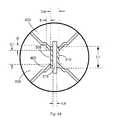
- FIG. 4Aillustrates various dimensions (Cw, Ch, Lw, and Lh) of the channel 305 and link 315 that may be adjusted according to various embodiments.
- Typical channels and linksare patterned to overlap and have a generally square geometry with matching surface area sizes. That is, dimension Lw and Ch may match, and dimensions Lh and Cw may match.
- Applicanthas observed that the RCtc associated with the horizontally and vertically arranged electrodes can be varied somewhat by adjusting the sizes of the channels and links.
- Table 1summarizes the results of various RCtc simulation results associated with electrode sensor matrices with different channel and link dimensions.
- each of the electrode sensor matricesutilizes a diamond-shape pad with a surface area of about 18 mm 2 .
- Sixty-four padsare arranged within each horizontally arranged electrode, and thirty-six pads are arranged within each vertically arranged electrode.
- the RCtc associated with the horizontally arranged electrodeis larger than the RCtc associated with the vertically arranged electrode due to its increased length and, therefore, represents a worst-case RCtc of the matrix. Only horizontal electrode RCtc values are shown in Table 1.
- the RCtc of a electrodemay be determined from the resistance per pad, R, and number of pads per electrode, n, and effective capacitance per pad, C, of the electrode which, in this case, is the horizontally arranged electrode.
- the resistance, Rmay be determined by dividing the total electrode resistance by the number of pads in the electrode.
- the effective capacitance, Ccorresponds to coupling capacitance between a given pad and its neighboring pads and to ground.
- the electrode sensor matrix that utilizes channels and links with respective widths and height (Cw, Ch, Lw, and Lh) of about 0.4 mmhas the lowest horizontal RCtc, which was determined to be 8.96 ⁇ s.
- Table 2summarizes the results when asymmetric shapes are utilized for the channels 305 and links 315 instead of square shapes.
- asymmetric shapesit was observed that the worst case RCtc was not always associated with the longer electrode axis (i.e., horizontally arranged electrode). Therefore, the RCtc of both the horizontally and vertically arranged electrodes were measured for various dimensional combinations of the channels 305 and links 315 .
- the lowest overall RCtcis associated with a channel with a width, Cw, of 0.4 mm and a height, Ch, of 1.0 mm, and a link with a width, Lw, of 0.2 mm and height, Lh, of 1.2 mm.
- the worst-case RCtcis 6.04 ⁇ s and is associated with the horizontally arranged electrode.
- the RCtc for the horizontally and vertically arranged electrodesare within ⁇ 50% of each other, and preferably ⁇ 10%, and more preferably ⁇ 2% of each other. That is, the RCtc of the respective sensors essentially match.
- the sheet resistance of the material used to form the channels 305 and links 315was assumed to be the same for the matrices determined above.
- the channels 305 and links 315were assumed to have a sheet resistance of 150 ⁇ /sq.
- the materials used to pattern the channels 305 and the links 315are different.
- the sheet resistance of the material used to pattern the links 315may, for example, be 200 ⁇ /sq.
- Table 3summarizes the results when such a material is used for the links 315 .
- the channels and links of the matriceswere arranged as described earlier.
- the combination with the lowest overall RCtcis represented in the fourth column.
- the channel 305has a width, Cw, of 0.4 mm and height, Ch, of 1.1 mm.
- the link 315has a width, Lw, of 0.2 mm and height, Lh, of 1.3 mm.
- the worst-case RCtcis 6.28 ⁇ s and is associated with the vertically arranged electrode.
- FIG. 4Bshows an alternate channel geometry that is possible when the link width, Lw, is substantially narrower than the channel width, Cw, as is the case with for the channel of FIG. 4A .
- the modified channel geometryfacilitates the reduction of channel resistance and, therefore, a reduction in the RCtc for the horizontally arranged electrodes, by gradually narrowing the channel height, Ch, of the horizontally arranged electrode as approaches the edge of the insulator 310 .
- the dashed lines 405 in FIG. 4Brepresents the geometry of the gap between vertical and horizontally arranged electrodes in FIG. 4A and are shown to illustrate the difference between the channel geometries of FIGS. 4A and 4B .
- the channel geometry of FIG. 4Breduces the current path length for which the channel is most constricted.
- the channel width Cw for the design of FIG. 4Bis smaller than the channel width Cw of FIG. 4A by an amount of 2 ⁇ where ⁇ is the length of the horizontal kink in the electrode boundaries as shown in FIG. 4B .
- Representative values of ⁇are in the range from 100 microns to 400 microns with 200 microns being a typical value.
- the height of the horizontal electrode at the kink of length ⁇is greater than the channel height Ch by an amount 2 ⁇ where ⁇ is the vertical offset of the kink relative to the channel boundaries as shown in FIG. 4B .
- it is desirable that the kink vertical offset ⁇is larger than the kink length ⁇ .
- kink vertical offset ⁇are in the range from 300 microns to 1,200 microns with 600 microns being a typical value. Corners in the electrode boundaries can be rounded and smoothed and the design will still provide substantially the same benefits.
- the essential feature of the design of FIG. 4Bis a modified electrode boundary geometry in which the channel width Cw is reduced in a way that reduces the horizontal electrode resistance while to a good engineering approximation retaining a similar area and geometry of the diamond shaped pads that compose the electrodes. This, in turn, reduces the horizontal electrode resistance and hence RCtc while having substantially no effect on vertical electrode resistance of RCtc.
- the horizontal electrode read out speed(more particularly the excitation drive frequency) is limited by the horizontal RCtc and the vertical electrode read out speed is limited by the vertical RCtc. If the same read out speed is used for both vertical and horizontal electrodes in self-capacitance mode, there is a clear advantage to minimizing the larger or worst-case of the horizontal and vertical RCtc values.
- the horizontal and vertical RCtc valuescontribute to a mutual-capacitance settling time that limits the read out speed of mutual capacitances. While the mathematical details of how horizontal and vertical RCtc values combine for mutual capacitance readout is complex, it is still of benefit to balance horizontal and vertical RCtc values to provide faster mutual-capacitance readout.
- varying the dimensions of the channels and linksallows for the reduction in RCtc and matching of the RCtc associated with the horizontally and vertically arranged electrodes. This in turn facilitates faster acquisition of a touch location, which ultimately results in a more pleasant user experience.
Landscapes
- Engineering & Computer Science (AREA)
- General Engineering & Computer Science (AREA)
- Theoretical Computer Science (AREA)
- Human Computer Interaction (AREA)
- Physics & Mathematics (AREA)
- General Physics & Mathematics (AREA)
- Position Input By Displaying (AREA)
Abstract
Description
- 1. Field
- The subject matter disclosed herein relates generally to capacitive touch sensors, and more particularly to a projected capacitive touch sensor with an asymmetric bridge pattern.
- 2. Description of Related Art
- Projected capacitive touch sensors typically include a substrate upon which sensing electrodes are disposed. The substrate may be a durable glass having high optical transparency for viewing images displayed by an underlying display device that displays images such as graphical buttons and icons. When a user touches the outer surface of the substrate at a location corresponding to a desired selection displayed on the display device, the location is determined by sensing a change in the capacitance of the sensing electrodes.
- In some projected capacitive touch sensors, the sensing electrodes are arranged in rows and columns. The rows and columns comprise pads that are generally arranged in the form of a matrix. Horizontally adjacent pads in a given row of the matrix are connected together to form a single horizontally arranged electrode. Although, in some projected capacitive touch sensors, the horizontally arranged electrodes may be split so that they do not span the entire sensor. Likewise, vertically adjacent pads in a given column are connected together to form a single vertically arranged electrode, and vertical electrodes like horizontal electrodes optionally may be split.
- Typically commercial projected capacitive touch sensor products are constructed from a lamination of at least two layers of glass in which horizontal electrodes and vertical electrodes are on different glass surfaces. For example, horizontal electrodes may be on one surface of a glass layer and the vertical electrodes on the opposite surface of the same glass layer. Alternatively horizontal and vertical electrodes may be fabricated on different glass layers. In either case, there is manufacturing cost associated with lamination of more than one piece of glass and with the fabrication of electrodes on more than one surface. Alternate designs in which both horizontal and vertical electrodes are fabricated on only one glass surface promise reduced manufacturing cost, particularly if the projected capacitive touch sensor includes only one glass layer with no lamination.
- To facilitate both horizontally arranged and vertically arranged electrodes on a single surface, bridging connections may be utilized to connect adjacent pads of a given electrode orientation. For example, bridging connections may couple the vertically adjacent pads that form the vertically arranged electrodes. Known bridging connections have a substantially square geometry. That is, the width and height of the bridge connections are the same.
- Associated with each electrode is resistance and capacitance, both of which depend on the size of the touch sensor. As the linear dimensions, of the touch sensor increase, so do the resistances and capacitances associated with the electrodes. The resulting resistor-capacitor time constant (RCtc) representative of electronic settling times of the touch sensor tend to grow quadradically with touch sensor size as both resistance and capacitance grow linearly. For small projected capacitive touch sensors used in smart phones or tablet computers, electronic settling times are less of an issue. However, for touch sensors designed for 15″ diagonal displays and larger displays, long touch sensor electronic settling times become more problematic.
- One problem with such large projected capacitive touch sensors is that the resistor-capacitor time constant (RCtc) of the horizontally and vertically arranged electrodes tends to be high and do not match. For example, a typical RCtc for such a large projected capacitive touch sensor may be 9 μS or higher. This is especially problematic when used in conjunction with fixed drive frequency controllers in which the total scan time is determined by the maximum RCTc of the arranged electrodes. The higher the RCtc, the more time that is needed to sense a capacitance value of the electrode. This in turn impacts the rate at which a touch location can be determined, which may negatively impact user experience.
- Electronics may read-out projected capacitive touch sensitive devices in either self-capacitive mode, mutual-capacitive, or a mixed mode, which is combination of the two. In self-capacitive mode, electronics measures one capacitance per electrode. In mutual capacitance mode, or all-points-addressable (APA) mode, electronics measures capacitance between a row electrode and a column electrode. In either case, the capacitance changes when a finger approaches the electrode. The same projected capacitive touch sensor construction may support self-capacitive mode, mutual-capacitive mode and mixed mode electronic read out.
- In a first aspect, a capacitive touch sensitive device includes a matrix of pads patterned in a first electrically conductive material on a substrate. Horizontally adjacent pads within each even row of the matrix are electrically coupled to one another via channels to form a plurality of horizontally arranged electrodes. Insulators are positioned over respective channels. Conductive links are formed over respective insulators and are configured to electrically couple vertically adjacent pads between odd rows of the matrix to form a plurality of vertically arranged electrodes. The dimensions of the channels and the conductive links are configured such that an RCtc of each of the vertically arranged electrodes substantially matches an RCtc of each of the horizontally arranged electrodes.
- In a second aspect, a method of manufacturing a capacitive touch sensitive device includes patterning a matrix of pads in a first electrically conductive material on a substrate. Horizontally adjacent pads within each even row of the matrix are electrically coupled to one another via channels to form a plurality of horizontally arranged electrodes. The method also includes forming insulators over respective channels from an insulator and forming conductive links over respective insulators configured to electrically couple vertically adjacent pads between odd rows of the matrix to form a plurality of vertically arranged electrodes. The dimensions of the channels and the conductive links are configured such that an RCtc of each of the vertically arranged electrodes substantially matches an RCtc of each of the horizontally arranged electrodes.
- In a third aspect, a capacitive touch sensitive device includes a matrix of pads patterned in a first electrically conductive material on a substrate. Horizontally adjacent pads within each even row of the matrix are electrically coupled to one another via channels to form a plurality of horizontally arranged electrodes. Insulators are positioned over respective channels. Conductive links are formed over respective insulators and are configured to electrically couple vertically adjacent pads between odd rows of the matrix to form a plurality of vertically arranged electrodes. The dimensions of the channels and the conductive links are configured such that an RCtc of each of the vertically arranged electrodes substantially matches an RCtc of each of the horizontally arranged electrodes. The total number of vertically arranged electrodes is different than a total number of horizontally arranged electrodes, and the RCtc of each of the vertically arranged electrodes and the horizontally arranged electrodes is less than 6.5 μS and is within ±50% of each other.
- The accompanying drawings are included to provide a further understanding of the claims, are incorporated in, and constitute a part of this specification. The detailed description and illustrated embodiments described serve to explain the principles defined by the claims.
FIG. 1 illustrates a capacitive touch sensitive device;FIG. 2 illustrates details of a portion of an electrode matrix of the capacitive touch sensitive device;FIGS. 3A-3C illustrate different elements of the electrode matrix that facilitate coupling of pads of the matrix to form horizontally and vertically arranged electrodes;FIG. 4A illustrates various dimensions of channels and links that couple adjacent pads that may be adjusted according to various embodiments; andFIG. 4B illustrates an alternative channel geometry that facilities in the reduction of resistance along a horizontally arranged electrode.- The embodiments described below overcome the problems discussed above by utilizing connections with asymmetric elements to couple the pads of the horizontally and vertically arranged electrodes.
FIG. 1 illustrates capacitive touchsensitive device 100. Thedevice 100 includes asubstrate 105 upon which aelectrode matrix 110 is arranged. Theelectrode matrix 110 includes a group of horizontally arranged electrodes and vertically arranged electrodes. In one exemplary embodiment, to accommodate a 16:9 display aspect ratio, the horizontally and vertically arranged electrodes fit within a rectangular area of the substrate that has a width, W, of about 477 mm and a height, H, of about 270 mm. Sixty-four vertically arranged electrodes and thirty-six horizontally arranged electrodes may be positioned within that area. In other words, the ratio of the number of vertically arranged electrodes to horizontally arranged electrodes may be about a 16:9. It is understood, however, that the principles disclosed herein may be adapted to accommodate different display sizes and a different number of horizontally and vertically arranged electrodes.FIG. 2 illustrates details of a portion of theelectrode matrix 110. Thematrix 110 is generally composed of a group ofpads 205 arranged in rows and columns. In one exemplary embodiment, eachpad 205 has a generally diamond shape and has an area of about 18 mm2. Thepads 205 may be patterned by etching an electrically conductive material layer previously deposited on a surface of thesubstrate 105, such as indium-tin-oxide (ITO). The sheet resistance of the electrically conductive material layer may be about 150 Ω/sq. However, different conductive materials may be used, and thepads 205 may be patterned differently and/or have a different shape.- In one implementation, horizontally
adjacent pads 205 within every other row210 (e.g., even rows) of thematrix 110 are electrically coupled to one another to collectively form horizontally arrangedelectrodes 210 that span substantially the entire width, W, of the capacitive touchsensitive device 100. In other implementations, a given row may include multiple horizontally arranged electrodes that each group a subset of the pads in the row, for example a horizontal row may be split into left and right electrodes.Pads 205 in the other rows (e.g., odd rows) are coupled to one another column-wise to collectively form vertically arrangedelectrodes 215 that span substantially the entire height, H, of the capacitive touchsensitive device 100. The horizontally arrangedelectrodes 210 are utilized to determine the vertical coordinate of a touch. The vertically arrangedelectrodes 215 are utilized to determine the horizontal coordinate of the touch. FIGS. 3A-3C illustrate different elements of thematrix 100 that facilitate coupling of thepads 205 to form the horizontally and vertically arranged electrodes (210,215). Referring toFIG. 3A ,channels 305 couple the horizontallyadjacent pads 205 of the horizontally arrangedelectrode 210. Thechannels 305 may be formed from the same electrically conductive material layer used to form thepads 205 and may be patterned at the same time as thepads 205. For example, an electrically conductive material may be uniformly deposited on thesubstrate 105. A mask that defines the pattern ofFIG. 3A may be used to selectively remove unwanted conductive material to define the pattern ofFIG. 3A .- Referring to
FIG. 3B ,insulators 310 may be formed over thechannels 305, and inFIG. 3C ,links 315 made of a conductive material may be deposited over theinsulators 310 to couple verticallyadjacent pads 205 of the vertically arrangedelectrodes 215. Theinsulators 310 may be formed from an insulating material such as a polymer or ceramic. For example, glass paste part number NP-7770B1 from Noritake Corp or ceramic part number G3-5679 from Okuno Corp. may be utilized for the insulating material. - The insulators are sized to prevent a short circuit between the
links 315 and thechannels 305 below, even when there are reasonable registration tolerances or errors during manufacture. That is, theinsulators 310 may be slightly larger than the portion of thechannels 305 over which thelinks 315 are deposited. Thelinks 315 may be formed from the same transparent conductive material used to form thepads 205 or a different material. In one exemplary embodiment, thelinks 315 are formed from a conductive material with a sheet resistance of about 200 Ω/sq. FIG. 4A illustrates various dimensions (Cw, Ch, Lw, and Lh) of thechannel 305 and link315 that may be adjusted according to various embodiments. Typical channels and links are patterned to overlap and have a generally square geometry with matching surface area sizes. That is, dimension Lw and Ch may match, and dimensions Lh and Cw may match. Applicant has observed that the RCtc associated with the horizontally and vertically arranged electrodes can be varied somewhat by adjusting the sizes of the channels and links.- Table 1 summarizes the results of various RCtc simulation results associated with electrode sensor matrices with different channel and link dimensions. In conventional designs, each of the electrode sensor matrices utilizes a diamond-shape pad with a surface area of about 18 mm2. Sixty-four pads are arranged within each horizontally arranged electrode, and thirty-six pads are arranged within each vertically arranged electrode. The RCtc associated with the horizontally arranged electrode is larger than the RCtc associated with the vertically arranged electrode due to its increased length and, therefore, represents a worst-case RCtc of the matrix. Only horizontal electrode RCtc values are shown in Table 1. The RCtc of a electrode may be determined from the resistance per pad, R, and number of pads per electrode, n, and effective capacitance per pad, C, of the electrode which, in this case, is the horizontally arranged electrode. The resistance, R, may be determined by dividing the total electrode resistance by the number of pads in the electrode. The effective capacitance, C, corresponds to coupling capacitance between a given pad and its neighboring pads and to ground. The resistor-capacitor time constant associated with an electrode with n pads is given by RCtc=(nR)·(nC)=n2RC.
- As shown, the electrode sensor matrix that utilizes channels and links with respective widths and height (Cw, Ch, Lw, and Lh) of about 0.4 mm has the lowest horizontal RCtc, which was determined to be 8.96 μs.
TABLE 1 Size (Lw × Ch) (mm) 1.0 × 1.0 0.5 × 0.5 0.4 × 0.4 0.3 × 0.3 0.2 × 0.2 R (Ω) 540 676 732 810 934 C (pF) 6 3.32 2.99 2.72 2.51 Horizontal 13.27 9.19 8.96 9.02 μs 9.6 μs RCtc (μs) - Table 2 summarizes the results when asymmetric shapes are utilized for the
channels 305 andlinks 315 instead of square shapes. For asymmetric shapes, it was observed that the worst case RCtc was not always associated with the longer electrode axis (i.e., horizontally arranged electrode). Therefore, the RCtc of both the horizontally and vertically arranged electrodes were measured for various dimensional combinations of thechannels 305 and links315. As shown, the lowest overall RCtc is associated with a channel with a width, Cw, of 0.4 mm and a height, Ch, of 1.0 mm, and a link with a width, Lw, of 0.2 mm and height, Lh, of 1.2 mm. The worst-case RCtc is 6.04 μs and is associated with the horizontally arranged electrode. The RCtc for the horizontally and vertically arranged electrodes are within ±50% of each other, and preferably ±10%, and more preferably ±2% of each other. That is, the RCtc of the respective sensors essentially match. TABLE 2 Channel (Cw × Ch) 0.4 × 0.6 1.0 × 1.0 1.0 × 1.1 1.0 × 0.9 0.4 × 0.9 0.4 × 0.8 0.4 × 1.0 0.4 × 1.1 Link (Lw × Lh) (mm) 0.4 × 0.6 0.2 × 1.2 0.2 × 1.3 0.2 × 1.1 0.2 × 1.1 0.2 × 1.0 0.2 × 1.2 0.2 × 1.3 Horizontal R (Ω) 732 521 493 553 482 510 459 439 C (pF) 2.99 2.99 3.17 2.91 3.11 3.03 3.21 3.26 RCtc (μs) 8.96 6.38 6.40 6.59 6.14 6.33 6.04 5.86 Vertical R (Ω) 732 1515 1583 1447 1447 1379 1515 1583 C (pF) 2.99 2.87 3.03 2.76 2.95 2.90 3.04 3.06 RCtc (μs) 2.94 5.63 6.21 5.18 5.53 5.18 5.97 6.28 - The sheet resistance of the material used to form the
channels 305 andlinks 315 was assumed to be the same for the matrices determined above. For example, thechannels 305 andlinks 315 were assumed to have a sheet resistance of 150 Ω/sq. However, this may not always be practical. In some exemplary embodiments, the materials used to pattern thechannels 305 and thelinks 315 are different. The sheet resistance of the material used to pattern thelinks 315 may, for example, be 200 Ω/sq. - Table 3 summarizes the results when such a material is used for the
links 315. The channels and links of the matrices were arranged as described earlier. The combination with the lowest overall RCtc is represented in the fourth column. In this case, thechannel 305 has a width, Cw, of 0.4 mm and height, Ch, of 1.1 mm. Thelink 315 has a width, Lw, of 0.2 mm and height, Lh, of 1.3 mm. The worst-case RCtc is 6.28 μs and is associated with the vertically arranged electrode. TABLE 3 Channel (Cw × Ch) 0.4 × 0.9 0.4 × 0.8 0.4 × 1.0 0.4 × 1.1 Link (Lw × Lh) (mm) 0.2 × 1.1 0.2 × 1.0 0.2 × 1.2 0.2 × 1.3 Horizontal R (Ω) 482 510 479 457 C (pF) 3.11 3.03 3.21 3.26 RCtc (μs) 6.14 μs 6.33 μs 6.30 μs 6.10 μs Vertical R (Ω) 1723 1630 1515 1583 C (pF) 2.95 2.90 3.04 3.06 RCtc (μs) 6.59 μs 6.13 μs 5.97 μs 6.28 μs FIG. 4B shows an alternate channel geometry that is possible when the link width, Lw, is substantially narrower than the channel width, Cw, as is the case with for the channel ofFIG. 4A . The modified channel geometry facilitates the reduction of channel resistance and, therefore, a reduction in the RCtc for the horizontally arranged electrodes, by gradually narrowing the channel height, Ch, of the horizontally arranged electrode as approaches the edge of theinsulator 310. The dashedlines 405 inFIG. 4B represents the geometry of the gap between vertical and horizontally arranged electrodes inFIG. 4A and are shown to illustrate the difference between the channel geometries ofFIGS. 4A and 4B . The channel geometry ofFIG. 4B reduces the current path length for which the channel is most constricted. The channel width Cw for the design ofFIG. 4B is smaller than the channel width Cw ofFIG. 4A by an amount of 2δ where δ is the length of the horizontal kink in the electrode boundaries as shown inFIG. 4B . Representative values of δ are in the range from 100 microns to 400 microns with 200 microns being a typical value. The height of the horizontal electrode at the kink of length δ is greater than the channel height Ch by an amount 2Δ where Δ is the vertical offset of the kink relative to the channel boundaries as shown inFIG. 4B . To receive the full benefit of the shortened channel width Cw, it is desirable that the kink vertical offset Δ is larger than the kink length δ. Representative values of the kink vertical offset Δ are in the range from 300 microns to 1,200 microns with 600 microns being a typical value. Corners in the electrode boundaries can be rounded and smoothed and the design will still provide substantially the same benefits. The essential feature of the design ofFIG. 4B is a modified electrode boundary geometry in which the channel width Cw is reduced in a way that reduces the horizontal electrode resistance while to a good engineering approximation retaining a similar area and geometry of the diamond shaped pads that compose the electrodes. This, in turn, reduces the horizontal electrode resistance and hence RCtc while having substantially no effect on vertical electrode resistance of RCtc.- For projected capacitive touch sensor that are read out in self-capacitance mode, the horizontal electrode read out speed (more particularly the excitation drive frequency) is limited by the horizontal RCtc and the vertical electrode read out speed is limited by the vertical RCtc. If the same read out speed is used for both vertical and horizontal electrodes in self-capacitance mode, there is a clear advantage to minimizing the larger or worst-case of the horizontal and vertical RCtc values. For projected capacitive touch screen that are read out in mutual-capacitance mode, the horizontal and vertical RCtc values contribute to a mutual-capacitance settling time that limits the read out speed of mutual capacitances. While the mathematical details of how horizontal and vertical RCtc values combine for mutual capacitance readout is complex, it is still of benefit to balance horizontal and vertical RCtc values to provide faster mutual-capacitance readout.
- While the preferred embodiments described above are for projected capacitive touch sensors with horizontal and vertical electrodes on the same surface of the same glass (or polymer) layer, one skilled in the art will understand that balancing of horizontal and vertical values of RCtc also provide benefits for touch sensors with horizontal and vertical electrodes on different glass surfaces.
- As described, varying the dimensions of the channels and links allows for the reduction in RCtc and matching of the RCtc associated with the horizontally and vertically arranged electrodes. This in turn facilitates faster acquisition of a touch location, which ultimately results in a more pleasant user experience.
- While various embodiments have been described, it will be apparent to those of ordinary skill in the art that many more embodiments and implementations are possible that are within the scope of the claims. The various dimensions described above are merely exemplary and may be adjusted, for example, based upon the dimensions of the substrate, the number pads, the ratio of the number of pads in the different electrode orientations, the sheet material used for the conductive layers, etc. Accordingly, it will be apparent to those of ordinary skill in the art that many more embodiments and implementations are possible that are within the scope of the claims. Therefore, the embodiments described are only provided to aid in understanding the claims and do not limit the scope of the claims.
Claims (21)
Priority Applications (9)
| Application Number | Priority Date | Filing Date | Title |
|---|---|---|---|
| US13/451,253US9197208B2 (en) | 2012-04-19 | 2012-04-19 | Projected capacitive touch sensor with asymmetric bridge pattern |
| US14/395,295US9582125B2 (en) | 2012-04-19 | 2013-04-17 | Projected capacitive touch sensor with asymmetric bridge pattern field |
| EP13720646.2AEP2839362B1 (en) | 2012-04-19 | 2013-04-17 | Projected capacitive touch sensor with asymmetric bridge pattern |
| CN201380031737.3ACN104395869B (en) | 2012-04-19 | 2013-04-17 | Projected capacitive touch sensor with asymmetric bridge map interlinking case |
| PCT/US2013/036868WO2013158699A1 (en) | 2012-04-19 | 2013-04-17 | Projected capacitive touch sensor with asymmetric bridge pattern |
| JP2015507132AJP6355623B2 (en) | 2012-04-19 | 2013-04-17 | Projection-type capacitive touch sensor with asymmetric bridge pattern |
| TW102113864ATWI522874B (en) | 2012-04-19 | 2013-04-19 | Projected capacitive touch sensor with asymmetric bridge pattern |
| US14/836,026US10082914B2 (en) | 2012-04-19 | 2015-08-26 | Method of manufacturing a touch sensitive device |
| US15/445,885US10126898B2 (en) | 2012-04-19 | 2017-02-28 | Projected capacitive touch sensor with asymmetric bridge pattern |
Applications Claiming Priority (1)
| Application Number | Priority Date | Filing Date | Title |
|---|---|---|---|
| US13/451,253US9197208B2 (en) | 2012-04-19 | 2012-04-19 | Projected capacitive touch sensor with asymmetric bridge pattern |
Related Child Applications (5)
| Application Number | Title | Priority Date | Filing Date |
|---|---|---|---|
| US14/395,295ContinuationUS9582125B2 (en) | 2012-04-19 | 2013-04-17 | Projected capacitive touch sensor with asymmetric bridge pattern field |
| US14/395,295Continuation-In-PartUS9582125B2 (en) | 2012-04-19 | 2013-04-17 | Projected capacitive touch sensor with asymmetric bridge pattern field |
| PCT/US2013/036868ContinuationWO2013158699A1 (en) | 2012-04-19 | 2013-04-17 | Projected capacitive touch sensor with asymmetric bridge pattern |
| PCT/US2013/036868Continuation-In-PartWO2013158699A1 (en) | 2012-04-19 | 2013-04-17 | Projected capacitive touch sensor with asymmetric bridge pattern |
| US14/836,026ContinuationUS10082914B2 (en) | 2012-04-19 | 2015-08-26 | Method of manufacturing a touch sensitive device |
Publications (2)
| Publication Number | Publication Date |
|---|---|
| US20130277193A1true US20130277193A1 (en) | 2013-10-24 |
| US9197208B2 US9197208B2 (en) | 2015-11-24 |
Family
ID=49379096
Family Applications (3)
| Application Number | Title | Priority Date | Filing Date |
|---|---|---|---|
| US13/451,253Active2033-12-31US9197208B2 (en) | 2012-04-19 | 2012-04-19 | Projected capacitive touch sensor with asymmetric bridge pattern |
| US14/395,295Active2032-09-08US9582125B2 (en) | 2012-04-19 | 2013-04-17 | Projected capacitive touch sensor with asymmetric bridge pattern field |
| US14/836,026Active2032-11-13US10082914B2 (en) | 2012-04-19 | 2015-08-26 | Method of manufacturing a touch sensitive device |
Family Applications After (2)
| Application Number | Title | Priority Date | Filing Date |
|---|---|---|---|
| US14/395,295Active2032-09-08US9582125B2 (en) | 2012-04-19 | 2013-04-17 | Projected capacitive touch sensor with asymmetric bridge pattern field |
| US14/836,026Active2032-11-13US10082914B2 (en) | 2012-04-19 | 2015-08-26 | Method of manufacturing a touch sensitive device |
Country Status (1)
| Country | Link |
|---|---|
| US (3) | US9197208B2 (en) |
Cited By (4)
| Publication number | Priority date | Publication date | Assignee | Title |
|---|---|---|---|---|
| US20130313098A1 (en)* | 2012-05-25 | 2013-11-28 | Chunghwa Picture Tubes, Ltd. | Electrode array of touch panel |
| US9582125B2 (en) | 2012-04-19 | 2017-02-28 | Elo Touch Solutions, Inc. | Projected capacitive touch sensor with asymmetric bridge pattern field |
| US10126898B2 (en) | 2012-04-19 | 2018-11-13 | Elo Touch Solutions, Inc. | Projected capacitive touch sensor with asymmetric bridge pattern |
| CN108845723A (en)* | 2018-07-19 | 2018-11-20 | 武汉华星光电半导体显示技术有限公司 | Touch panel and touch-control display panel |
Families Citing this family (4)
| Publication number | Priority date | Publication date | Assignee | Title |
|---|---|---|---|---|
| US20150091842A1 (en)* | 2013-09-30 | 2015-04-02 | Synaptics Incorporated | Matrix sensor for image touch sensing |
| US10042489B2 (en) | 2013-09-30 | 2018-08-07 | Synaptics Incorporated | Matrix sensor for image touch sensing |
| KR20170105330A (en)* | 2016-03-09 | 2017-09-19 | 삼성전자주식회사 | Touch Panel and Electronic Device involving the same |
| KR102491224B1 (en)* | 2017-06-01 | 2023-01-20 | 엘지디스플레이 주식회사 | Touch display device and touch panel |
Citations (5)
| Publication number | Priority date | Publication date | Assignee | Title |
|---|---|---|---|---|
| US20100207891A1 (en)* | 2009-02-19 | 2010-08-19 | Eturbotouch Technology, Inc. | Structural improvement to touch panel |
| US20100321328A1 (en)* | 2009-06-17 | 2010-12-23 | Novatek Microelectronics Corp. | Coordinates algorithm and position sensing system of touch panel |
| US20110139516A1 (en)* | 2009-12-16 | 2011-06-16 | 3M Innovative Properties Company | Touch sensitive device with multilayer electrode having improved optical and electrical performance |
| US8593410B2 (en)* | 2009-04-10 | 2013-11-26 | Apple Inc. | Touch sensor panel design |
| US20130321341A1 (en)* | 2011-02-22 | 2013-12-05 | Sharp Kabushiki Kaisha | Coordinate input device, and electronic device |
Family Cites Families (44)
| Publication number | Priority date | Publication date | Assignee | Title |
|---|---|---|---|---|
| US4320418A (en)* | 1978-12-08 | 1982-03-16 | Pavliscak Thomas J | Large area display |
| US4639720A (en) | 1981-01-12 | 1987-01-27 | Harris Corporation | Electronic sketch pad |
| US4550221A (en) | 1983-10-07 | 1985-10-29 | Scott Mabusth | Touch sensitive control device |
| US5543590A (en) | 1992-06-08 | 1996-08-06 | Synaptics, Incorporated | Object position detector with edge motion feature |
| GB9406702D0 (en) | 1994-04-05 | 1994-05-25 | Binstead Ronald P | Multiple input proximity detector and touchpad system |
| US6288707B1 (en)* | 1996-07-29 | 2001-09-11 | Harald Philipp | Capacitive position sensor |
| US7463246B2 (en) | 2002-06-25 | 2008-12-09 | Synaptics Incorporated | Capacitive sensing device |
| US20050030048A1 (en)* | 2003-08-05 | 2005-02-10 | Bolender Robert J. | Capacitive sensing device for use in a keypad assembly |
| US8166649B2 (en)* | 2005-12-12 | 2012-05-01 | Nupix, LLC | Method of forming an electroded sheet |
| US20070229470A1 (en)* | 2006-03-31 | 2007-10-04 | Warren Snyder | Capacitive touch sense device having polygonal shaped sensor elements |
| US8619054B2 (en)* | 2006-05-31 | 2013-12-31 | Atmel Corporation | Two dimensional position sensor |
| TW200842681A (en)* | 2007-04-27 | 2008-11-01 | Tpk Touch Solutions Inc | Touch pattern structure of a capacitive touch panel |
| US20080297174A1 (en) | 2007-05-31 | 2008-12-04 | Sarangan Narasimhan | Capacitive sensing devices |
| US20090194344A1 (en) | 2008-01-31 | 2009-08-06 | Avago Technologies Ecbu Ip (Singapore) Pte. Ltd. | Single Layer Mutual Capacitance Sensing Systems, Device, Components and Methods |
| EP2113827B8 (en) | 2008-04-30 | 2018-09-19 | InnoLux Corporation | Touch input device |
| JP4720857B2 (en)* | 2008-06-18 | 2011-07-13 | ソニー株式会社 | Capacitance type input device and display device with input function |
| US7735383B2 (en) | 2008-06-24 | 2010-06-15 | Synaptics Incorporated | Balanced resistance capacitive sensing apparatus |
| JP5154316B2 (en) | 2008-06-30 | 2013-02-27 | 株式会社ジャパンディスプレイイースト | Touch panel |
| JP5033078B2 (en) | 2008-08-06 | 2012-09-26 | 株式会社ジャパンディスプレイイースト | Display device |
| JP2010108222A (en) | 2008-10-30 | 2010-05-13 | Kyocera Corp | Touch panel and touch panel type display device |
| TWI471789B (en) | 2008-11-14 | 2015-02-01 | Wintek Corp | Touch panel |
| JP2010123674A (en) | 2008-11-18 | 2010-06-03 | Panasonic Corp | Semiconductor laser device |
| US8274486B2 (en) | 2008-12-22 | 2012-09-25 | Flextronics Ap, Llc | Diamond pattern on a single layer |
| US8115751B2 (en) | 2008-12-30 | 2012-02-14 | Young Fast Optoelectronics Co., Ltd. | Capacitive touch sensing assembly |
| US9075484B2 (en) | 2009-06-02 | 2015-07-07 | Pixart Imaging Inc. | Sensor patterns for mutual capacitance touchscreens |
| TWI380209B (en) | 2009-06-18 | 2012-12-21 | Au Optronics Corp | Touch panel |
| JP5418130B2 (en) | 2009-10-15 | 2014-02-19 | 大日本印刷株式会社 | Capacitive touch panel sensor and method for manufacturing the touch panel sensor |
| CN101699384B (en) | 2009-10-15 | 2011-12-07 | 深超光电(深圳)有限公司 | Touch panel |
| JP2012014669A (en)* | 2009-11-20 | 2012-01-19 | Fujifilm Corp | Conductive sheet, method of using conductive sheet and electrostatic capacitive touch panel |
| KR101351415B1 (en) | 2009-12-09 | 2014-01-16 | 엘지디스플레이 주식회사 | Touch Panel and Liquid Crystal Display Device including Touch Panel |
| JP2011180806A (en) | 2010-03-01 | 2011-09-15 | Hitachi Displays Ltd | Touch panel and display device |
| KR101101053B1 (en) | 2010-03-16 | 2011-12-29 | 삼성모바일디스플레이주식회사 | Touch screen panel and its manufacturing method |
| JP2011227840A (en) | 2010-04-23 | 2011-11-10 | Hitachi Ltd | Apparatus for controlling transmission/reception of core license between servers in non-smp configuration |
| CN201773378U (en) | 2010-05-04 | 2011-03-23 | 宸鸿科技(厦门)有限公司 | Touch panel and touch display device |
| US8780073B2 (en) | 2010-05-24 | 2014-07-15 | Cypress Semiconductor Corporation | Capacitive sensor arrangement |
| US8482546B2 (en) | 2010-06-30 | 2013-07-09 | Cypress Semiconductor Corporation | Self shielding capacitance sensing panel |
| JP5345980B2 (en) | 2010-07-09 | 2013-11-20 | 富士フイルム株式会社 | Transparent conductive substrate, conductive sheet for touch panel, and touch panel |
| US8519970B2 (en) | 2010-07-16 | 2013-08-27 | Perceptive Pixel Inc. | Capacitive touch sensor having correlation with a receiver |
| US20120019473A1 (en)* | 2010-07-21 | 2012-01-26 | Chimei Innolux Corporation | Systems for displaying images |
| KR101323004B1 (en)* | 2010-10-01 | 2013-10-29 | 엘지디스플레이 주식회사 | Capacity type touch screen panel |
| TWM410274U (en) | 2011-03-09 | 2011-08-21 | Derlead Invest Ltd | Projection-type capacitive touch panel with impedance fine-tuning structure |
| TWI453643B (en) | 2011-08-19 | 2014-09-21 | Innolux Corpration | Touch panel and electronic device |
| KR101415583B1 (en) | 2011-12-16 | 2014-07-07 | 엘지이노텍 주식회사 | Touch panel and forming method for the same |
| US9197208B2 (en) | 2012-04-19 | 2015-11-24 | Elo Touch Solutions, Inc. | Projected capacitive touch sensor with asymmetric bridge pattern |
- 2012
- 2012-04-19USUS13/451,253patent/US9197208B2/enactiveActive
- 2013
- 2013-04-17USUS14/395,295patent/US9582125B2/enactiveActive
- 2015
- 2015-08-26USUS14/836,026patent/US10082914B2/enactiveActive
Patent Citations (5)
| Publication number | Priority date | Publication date | Assignee | Title |
|---|---|---|---|---|
| US20100207891A1 (en)* | 2009-02-19 | 2010-08-19 | Eturbotouch Technology, Inc. | Structural improvement to touch panel |
| US8593410B2 (en)* | 2009-04-10 | 2013-11-26 | Apple Inc. | Touch sensor panel design |
| US20100321328A1 (en)* | 2009-06-17 | 2010-12-23 | Novatek Microelectronics Corp. | Coordinates algorithm and position sensing system of touch panel |
| US20110139516A1 (en)* | 2009-12-16 | 2011-06-16 | 3M Innovative Properties Company | Touch sensitive device with multilayer electrode having improved optical and electrical performance |
| US20130321341A1 (en)* | 2011-02-22 | 2013-12-05 | Sharp Kabushiki Kaisha | Coordinate input device, and electronic device |
Cited By (7)
| Publication number | Priority date | Publication date | Assignee | Title |
|---|---|---|---|---|
| US9582125B2 (en) | 2012-04-19 | 2017-02-28 | Elo Touch Solutions, Inc. | Projected capacitive touch sensor with asymmetric bridge pattern field |
| US10082914B2 (en) | 2012-04-19 | 2018-09-25 | Elo Touch Solutions, Inc. | Method of manufacturing a touch sensitive device |
| US10126898B2 (en) | 2012-04-19 | 2018-11-13 | Elo Touch Solutions, Inc. | Projected capacitive touch sensor with asymmetric bridge pattern |
| US20130313098A1 (en)* | 2012-05-25 | 2013-11-28 | Chunghwa Picture Tubes, Ltd. | Electrode array of touch panel |
| US8803019B2 (en)* | 2012-05-25 | 2014-08-12 | Chunghwa Picture Tubes, Ltd. | Electrode array of touch panel |
| CN108845723A (en)* | 2018-07-19 | 2018-11-20 | 武汉华星光电半导体显示技术有限公司 | Touch panel and touch-control display panel |
| US11137855B2 (en) | 2018-07-19 | 2021-10-05 | Wuhan China Star Optoelectronics Semiconductor Display Technology Co., Ltd. | Touch panel and touch display panel |
Also Published As
| Publication number | Publication date |
|---|---|
| US9197208B2 (en) | 2015-11-24 |
| US20150363025A1 (en) | 2015-12-17 |
| US10082914B2 (en) | 2018-09-25 |
| US9582125B2 (en) | 2017-02-28 |
| US20150138137A1 (en) | 2015-05-21 |
Similar Documents
| Publication | Publication Date | Title |
|---|---|---|
| US10082914B2 (en) | Method of manufacturing a touch sensitive device | |
| CN105808014B (en) | An array substrate, a method for making the same, and a touch display device | |
| US10126898B2 (en) | Projected capacitive touch sensor with asymmetric bridge pattern | |
| EP2113827B1 (en) | Touch input device | |
| EP2556423B1 (en) | Equalizing parasitic capacitance effects in touch screens | |
| TWI550453B (en) | Touch sensor electrodes, touch panels and display devices | |
| US20110193796A1 (en) | Touch screen panel | |
| TWI541712B (en) | Touch screen, touch panel, and driving method thereof | |
| US20110298731A1 (en) | Touch display device and touch display substrate thereof | |
| CN104503653B (en) | Self-capacitance touch screen and display device | |
| WO2012118038A1 (en) | Liquid crystal display device | |
| US9519383B2 (en) | ITO pattern for capacitive touchscreen applications | |
| US9927916B2 (en) | Touch detection device with sensor pads having bar-shaped strips | |
| CN107678596A (en) | The preparation method of touch base plate motherboard, touching display screen and touch-control display panel | |
| KR101707391B1 (en) | Touch detecting apparatus for hybrid scan type touch detecting | |
| US9335876B2 (en) | Cross-shaped touchscreen pattern | |
| US9401712B2 (en) | Touch panel substrate with first grid electrodes and second grid electrodes | |
| CN206877310U (en) | Touch induction device | |
| KR20240020773A (en) | How to layout the signal lines on the upper layer of the conductor | |
| KR20180069283A (en) | Multi point touch screen pannel | |
| KR20240038906A (en) | Object Location Detection Device | |
| KR20240038905A (en) | Object Location Detection Device | |
| KR20240038907A (en) | Object Location Detection Device | |
| KR20240020778A (en) | How to layout the signal lines on the upper layer of the conductor | |
| CN102103425A (en) | Touch panel with matrix electrode string and touch detection method |
Legal Events
| Date | Code | Title | Description |
|---|---|---|---|
| AS | Assignment | Owner name:TYCO ELECTRONICS CORPORATION, PENNSYLVANIA Free format text:ASSIGNMENT OF ASSIGNORS INTEREST;ASSIGNOR:SON, KYU-TAK;REEL/FRAME:028181/0943 Effective date:20120509 | |
| AS | Assignment | Owner name:ELO TOUCH SOLUTIONS, INC., CALIFORNIA Free format text:ASSIGNMENT OF ASSIGNORS INTEREST;ASSIGNOR:TYCO ELECTRONICS CORPORATION;REEL/FRAME:028357/0655 Effective date:20120601 | |
| STCF | Information on status: patent grant | Free format text:PATENTED CASE | |
| FEPP | Fee payment procedure | Free format text:PAT HOLDER CLAIMS SMALL ENTITY STATUS, ENTITY STATUS SET TO SMALL (ORIGINAL EVENT CODE: LTOS); ENTITY STATUS OF PATENT OWNER: LARGE ENTITY | |
| AS | Assignment | Owner name:JPMORGAN CHASE BANK, N.A., AS COLLATERAL AGENT, NEW YORK Free format text:SECURITY AGREEMENT;ASSIGNOR:ELO TOUCH SOLUTIONS, INC.;REEL/FRAME:044652/0421 Effective date:20171031 Owner name:JPMORGAN CHASE BANK, N.A., AS COLLATERAL AGENT, NE Free format text:SECURITY AGREEMENT;ASSIGNOR:ELO TOUCH SOLUTIONS, INC.;REEL/FRAME:044652/0421 Effective date:20171031 | |
| FEPP | Fee payment procedure | Free format text:ENTITY STATUS SET TO UNDISCOUNTED (ORIGINAL EVENT CODE: BIG.) | |
| AS | Assignment | Owner name:ELO TOUCH SOLUTIONS, INC., DELAWARE Free format text:RELEASE BY SECURED PARTY;ASSIGNOR:JPMORGAN CHASE BANK, N.A.;REEL/FRAME:047909/0833 Effective date:20181214 | |
| AS | Assignment | Owner name:GOLDMAN SACHS BANK USA, AS COLLATERAL AGENT, NEW JERSEY Free format text:SECURITY INTEREST;ASSIGNOR:ELO TOUCH SOLUTIONS, INC.;REEL/FRAME:047956/0114 Effective date:20181214 Owner name:GOLDMAN SACHS BANK USA, AS COLLATERAL AGENT, NEW J Free format text:SECURITY INTEREST;ASSIGNOR:ELO TOUCH SOLUTIONS, INC.;REEL/FRAME:047956/0114 Effective date:20181214 | |
| MAFP | Maintenance fee payment | Free format text:PAYMENT OF MAINTENANCE FEE, 4TH YEAR, LARGE ENTITY (ORIGINAL EVENT CODE: M1551); ENTITY STATUS OF PATENT OWNER: LARGE ENTITY Year of fee payment:4 | |
| MAFP | Maintenance fee payment | Free format text:PAYMENT OF MAINTENANCE FEE, 8TH YEAR, LARGE ENTITY (ORIGINAL EVENT CODE: M1552); ENTITY STATUS OF PATENT OWNER: LARGE ENTITY Year of fee payment:8 | |
| AS | Assignment | Owner name:ELO TOUCH SOLUTIONS, INC., TENNESSEE Free format text:ADDRESS CHANGE;ASSIGNOR:ELO TOUCH SOLUTIONS, INC.;REEL/FRAME:064571/0711 Effective date:20190613 | |
| AS | Assignment | Owner name:ELO TOUCH SOLUTIONS, INC., TENNESSEE Free format text:RELEASE OF SECURITY INTERESTS (FIRST LIEN) IN PATENTS;ASSIGNOR:GOLDMAN SACHS BANK USA;REEL/FRAME:070670/0714 Effective date:20250327 Owner name:CITIZENS BANK, N.A., MASSACHUSETTS Free format text:SECURITY INTEREST;ASSIGNOR:ELO TOUCH SOLUTIONS, INC.;REEL/FRAME:070666/0540 Effective date:20250327 |