US20130266326A1 - Microlenses for Multibeam Arrays of Optoelectronic Devices for High Frequency Operation - Google Patents
Microlenses for Multibeam Arrays of Optoelectronic Devices for High Frequency OperationDownload PDFInfo
- Publication number
- US20130266326A1 US20130266326A1US13/902,555US201313902555AUS2013266326A1US 20130266326 A1US20130266326 A1US 20130266326A1US 201313902555 AUS201313902555 AUS 201313902555AUS 2013266326 A1US2013266326 A1US 2013266326A1
- Authority
- US
- United States
- Prior art keywords
- optical device
- receiver
- light
- optical
- transmitter
- Prior art date
- Legal status (The legal status is an assumption and is not a legal conclusion. Google has not performed a legal analysis and makes no representation as to the accuracy of the status listed.)
- Granted
Links
- 238000003491arrayMethods0.000titledescription32
- 230000005693optoelectronicsEffects0.000titledescription6
- 230000003287optical effectEffects0.000claimsdescription161
- 239000000758substrateSubstances0.000claimsdescription87
- 230000005540biological transmissionEffects0.000claimsdescription16
- 239000012141concentrateSubstances0.000claimsdescription3
- 230000010287polarizationEffects0.000claimsdescription3
- 238000005286illuminationMethods0.000claims2
- 239000010410layerSubstances0.000description95
- 229910052751metalInorganic materials0.000description59
- 239000002184metalSubstances0.000description59
- 238000000034methodMethods0.000description57
- 239000000463materialSubstances0.000description35
- 230000008569processEffects0.000description27
- 238000013461designMethods0.000description22
- 238000000151depositionMethods0.000description20
- 230000004044responseEffects0.000description20
- 229920002120photoresistant polymerPolymers0.000description19
- 230000008021depositionEffects0.000description16
- 238000004891communicationMethods0.000description13
- 239000010931goldSubstances0.000description13
- 238000007747platingMethods0.000description11
- 239000004065semiconductorSubstances0.000description11
- 238000005530etchingMethods0.000description10
- 238000004519manufacturing processMethods0.000description9
- 150000002739metalsChemical class0.000description9
- 230000003071parasitic effectEffects0.000description9
- PXHVJJICTQNCMI-UHFFFAOYSA-NNickelChemical compound[Ni]PXHVJJICTQNCMI-UHFFFAOYSA-N0.000description8
- 238000001465metallisationMethods0.000description8
- 230000009467reductionEffects0.000description8
- 230000008901benefitEffects0.000description7
- 239000000835fiberSubstances0.000description7
- KDLHZDBZIXYQEI-UHFFFAOYSA-NPalladiumChemical compound[Pd]KDLHZDBZIXYQEI-UHFFFAOYSA-N0.000description6
- 230000000694effectsEffects0.000description6
- 229910000679solderInorganic materials0.000description6
- 235000012431wafersNutrition0.000description6
- JBRZTFJDHDCESZ-UHFFFAOYSA-NAsGaChemical compound[As]#[Ga]JBRZTFJDHDCESZ-UHFFFAOYSA-N0.000description5
- 239000011248coating agentSubstances0.000description5
- 238000000576coating methodMethods0.000description5
- 238000009792diffusion processMethods0.000description5
- 229910052737goldInorganic materials0.000description5
- 230000003647oxidationEffects0.000description5
- 238000007254oxidation reactionMethods0.000description5
- BASFCYQUMIYNBI-UHFFFAOYSA-NplatinumChemical compound[Pt]BASFCYQUMIYNBI-UHFFFAOYSA-N0.000description5
- 239000007787solidSubstances0.000description5
- 238000003892spreadingMethods0.000description5
- 239000010936titaniumSubstances0.000description5
- VHUUQVKOLVNVRT-UHFFFAOYSA-NAmmonium hydroxideChemical compound[NH4+].[OH-]VHUUQVKOLVNVRT-UHFFFAOYSA-N0.000description4
- 229910001218Gallium arsenideInorganic materials0.000description4
- XUIMIQQOPSSXEZ-UHFFFAOYSA-NSiliconChemical compound[Si]XUIMIQQOPSSXEZ-UHFFFAOYSA-N0.000description4
- 239000000460chlorineSubstances0.000description4
- 239000003989dielectric materialSubstances0.000description4
- PCHJSUWPFVWCPO-UHFFFAOYSA-NgoldChemical compound[Au]PCHJSUWPFVWCPO-UHFFFAOYSA-N0.000description4
- 238000010438heat treatmentMethods0.000description4
- 239000000203mixtureSubstances0.000description4
- 238000000206photolithographyMethods0.000description4
- 229910052710siliconInorganic materials0.000description4
- 239000010703siliconSubstances0.000description4
- 230000007480spreadingEffects0.000description4
- 238000007514turningMethods0.000description4
- 229910052581Si3N4Inorganic materials0.000description3
- 229910052782aluminiumInorganic materials0.000description3
- 238000013459approachMethods0.000description3
- 230000004888barrier functionEffects0.000description3
- 230000009286beneficial effectEffects0.000description3
- 230000007423decreaseEffects0.000description3
- 230000008020evaporationEffects0.000description3
- 238000001704evaporationMethods0.000description3
- 229910052738indiumInorganic materials0.000description3
- 238000001459lithographyMethods0.000description3
- 238000005259measurementMethods0.000description3
- 238000004806packaging method and processMethods0.000description3
- 229910052763palladiumInorganic materials0.000description3
- 238000000623plasma-assisted chemical vapour depositionMethods0.000description3
- 229910052697platinumInorganic materials0.000description3
- 238000012545processingMethods0.000description3
- 238000005086pumpingMethods0.000description3
- 239000000523sampleSubstances0.000description3
- 238000000926separation methodMethods0.000description3
- HQVNEWCFYHHQES-UHFFFAOYSA-Nsilicon nitrideChemical compoundN12[Si]34N5[Si]62N3[Si]51N64HQVNEWCFYHHQES-UHFFFAOYSA-N0.000description3
- 239000000243solutionSubstances0.000description3
- ZAMOUSCENKQFHK-UHFFFAOYSA-NChlorine atomChemical compound[Cl]ZAMOUSCENKQFHK-UHFFFAOYSA-N0.000description2
- 239000004593EpoxySubstances0.000description2
- GWEVSGVZZGPLCZ-UHFFFAOYSA-NTitan oxideChemical compoundO=[Ti]=OGWEVSGVZZGPLCZ-UHFFFAOYSA-N0.000description2
- 239000000853adhesiveSubstances0.000description2
- 230000001070adhesive effectEffects0.000description2
- FTWRSWRBSVXQPI-UHFFFAOYSA-Nalumanylidynearsane;gallanylidynearsaneChemical compound[As]#[Al].[As]#[Ga]FTWRSWRBSVXQPI-UHFFFAOYSA-N0.000description2
- XAGFODPZIPBFFR-UHFFFAOYSA-NaluminiumChemical compound[Al]XAGFODPZIPBFFR-UHFFFAOYSA-N0.000description2
- 239000000908ammonium hydroxideSubstances0.000description2
- 230000000712assemblyEffects0.000description2
- 238000000429assemblyMethods0.000description2
- 238000000231atomic layer depositionMethods0.000description2
- 230000015572biosynthetic processEffects0.000description2
- 229910052801chlorineInorganic materials0.000description2
- 239000011651chromiumSubstances0.000description2
- 238000004140cleaningMethods0.000description2
- 239000010949copperSubstances0.000description2
- 238000005520cutting processMethods0.000description2
- 230000007547defectEffects0.000description2
- 238000013400design of experimentMethods0.000description2
- 238000005516engineering processMethods0.000description2
- APFVFJFRJDLVQX-UHFFFAOYSA-Nindium atomChemical compound[In]APFVFJFRJDLVQX-UHFFFAOYSA-N0.000description2
- 238000001451molecular beam epitaxyMethods0.000description2
- 239000013307optical fiberSubstances0.000description2
- 230000000737periodic effectEffects0.000description2
- 229920000642polymerPolymers0.000description2
- 239000002096quantum dotSubstances0.000description2
- 239000002356single layerSubstances0.000description2
- 239000002904solventSubstances0.000description2
- 238000004544sputter depositionMethods0.000description2
- 238000012360testing methodMethods0.000description2
- XLYOFNOQVPJJNP-UHFFFAOYSA-NwaterSubstancesOXLYOFNOQVPJJNP-UHFFFAOYSA-N0.000description2
- IJGRMHOSHXDMSA-UHFFFAOYSA-NAtomic nitrogenChemical compoundN#NIJGRMHOSHXDMSA-UHFFFAOYSA-N0.000description1
- 229910015844BCl3Inorganic materials0.000description1
- KZBUYRJDOAKODT-UHFFFAOYSA-NChlorineChemical compoundClClKZBUYRJDOAKODT-UHFFFAOYSA-N0.000description1
- VYZAMTAEIAYCRO-UHFFFAOYSA-NChromiumChemical compound[Cr]VYZAMTAEIAYCRO-UHFFFAOYSA-N0.000description1
- RYGMFSIKBFXOCR-UHFFFAOYSA-NCopperChemical compound[Cu]RYGMFSIKBFXOCR-UHFFFAOYSA-N0.000description1
- 229910005540GaPInorganic materials0.000description1
- 241001101998GaliumSpecies0.000description1
- 229910000530Gallium indium arsenideInorganic materials0.000description1
- MHAJPDPJQMAIIY-UHFFFAOYSA-NHydrogen peroxideChemical compoundOOMHAJPDPJQMAIIY-UHFFFAOYSA-N0.000description1
- GPXJNWSHGFTCBW-UHFFFAOYSA-NIndium phosphideChemical compound[In]#PGPXJNWSHGFTCBW-UHFFFAOYSA-N0.000description1
- RTAQQCXQSZGOHL-UHFFFAOYSA-NTitaniumChemical compound[Ti]RTAQQCXQSZGOHL-UHFFFAOYSA-N0.000description1
- KXNLCSXBJCPWGL-UHFFFAOYSA-N[Ga].[As].[In]Chemical compound[Ga].[As].[In]KXNLCSXBJCPWGL-UHFFFAOYSA-N0.000description1
- 239000011149active materialSubstances0.000description1
- 229910045601alloyInorganic materials0.000description1
- 239000000956alloySubstances0.000description1
- 238000000137annealingMethods0.000description1
- QVGXLLKOCUKJST-UHFFFAOYSA-Natomic oxygenChemical compound[O]QVGXLLKOCUKJST-UHFFFAOYSA-N0.000description1
- 229910052790berylliumInorganic materials0.000description1
- ATBAMAFKBVZNFJ-UHFFFAOYSA-Nberyllium atomChemical compound[Be]ATBAMAFKBVZNFJ-UHFFFAOYSA-N0.000description1
- 230000002457bidirectional effectEffects0.000description1
- 238000004364calculation methodMethods0.000description1
- 238000005266castingMethods0.000description1
- 230000015556catabolic processEffects0.000description1
- 239000000919ceramicSubstances0.000description1
- 238000005229chemical vapour depositionMethods0.000description1
- 229910052804chromiumInorganic materials0.000description1
- 238000005253claddingMethods0.000description1
- 239000004020conductorSubstances0.000description1
- 229910052802copperInorganic materials0.000description1
- 239000013078crystalSubstances0.000description1
- 230000007123defenseEffects0.000description1
- 238000006731degradation reactionMethods0.000description1
- 230000001419dependent effectEffects0.000description1
- 238000001514detection methodMethods0.000description1
- 229910003460diamondInorganic materials0.000description1
- 239000010432diamondSubstances0.000description1
- 238000009826distributionMethods0.000description1
- 238000010894electron beam technologyMethods0.000description1
- 238000000609electron-beam lithographyMethods0.000description1
- 230000008030eliminationEffects0.000description1
- 238000003379elimination reactionMethods0.000description1
- 230000004927fusionEffects0.000description1
- HZXMRANICFIONG-UHFFFAOYSA-Ngallium phosphideChemical compound[Ga]#PHZXMRANICFIONG-UHFFFAOYSA-N0.000description1
- 239000007789gasSubstances0.000description1
- 239000011521glassSubstances0.000description1
- SAOPTAQUONRHEV-UHFFFAOYSA-Ngold zincChemical compound[Zn].[Au]SAOPTAQUONRHEV-UHFFFAOYSA-N0.000description1
- IXCSERBJSXMMFS-UHFFFAOYSA-Nhcl hclChemical compoundCl.ClIXCSERBJSXMMFS-UHFFFAOYSA-N0.000description1
- 230000020169heat generationEffects0.000description1
- 238000007731hot pressingMethods0.000description1
- 239000007943implantSubstances0.000description1
- RPQDHPTXJYYUPQ-UHFFFAOYSA-Nindium arsenideChemical compound[In]#[As]RPQDHPTXJYYUPQ-UHFFFAOYSA-N0.000description1
- 230000000977initiatory effectEffects0.000description1
- 238000001746injection mouldingMethods0.000description1
- 238000005468ion implantationMethods0.000description1
- 238000010884ion-beam techniqueMethods0.000description1
- 150000002500ionsChemical class0.000description1
- 238000003754machiningMethods0.000description1
- 238000007620mathematical functionMethods0.000description1
- 239000000155meltSubstances0.000description1
- 239000012528membraneSubstances0.000description1
- 238000012986modificationMethods0.000description1
- 230000004048modificationEffects0.000description1
- 238000012544monitoring processMethods0.000description1
- 229910052759nickelInorganic materials0.000description1
- 230000001151other effectEffects0.000description1
- 230000001590oxidative effectEffects0.000description1
- 239000001301oxygenSubstances0.000description1
- 229910052760oxygenInorganic materials0.000description1
- 238000012856packingMethods0.000description1
- 238000000059patterningMethods0.000description1
- 230000000704physical effectEffects0.000description1
- 239000002861polymer materialSubstances0.000description1
- 229910052761rare earth metalInorganic materials0.000description1
- 150000002910rare earth metalsChemical class0.000description1
- 238000002310reflectometryMethods0.000description1
- 230000001105regulatory effectEffects0.000description1
- 238000011160researchMethods0.000description1
- 230000002441reversible effectEffects0.000description1
- 238000000992sputter etchingMethods0.000description1
- 239000000126substanceSubstances0.000description1
- 229910052719titaniumInorganic materials0.000description1
- 238000012546transferMethods0.000description1
- 230000001131transforming effectEffects0.000description1
- 238000011282treatmentMethods0.000description1
- FAQYAMRNWDIXMY-UHFFFAOYSA-NtrichloroboraneChemical compoundClB(Cl)ClFAQYAMRNWDIXMY-UHFFFAOYSA-N0.000description1
- WFKWXMTUELFFGS-UHFFFAOYSA-NtungstenChemical compound[W]WFKWXMTUELFFGS-UHFFFAOYSA-N0.000description1
- 229910052721tungstenInorganic materials0.000description1
- 239000010937tungstenSubstances0.000description1
- 230000005641tunnelingEffects0.000description1
- 238000003466weldingMethods0.000description1
- 239000002023woodSubstances0.000description1
Images


Classifications
- H—ELECTRICITY
- H01—ELECTRIC ELEMENTS
- H01S—DEVICES USING THE PROCESS OF LIGHT AMPLIFICATION BY STIMULATED EMISSION OF RADIATION [LASER] TO AMPLIFY OR GENERATE LIGHT; DEVICES USING STIMULATED EMISSION OF ELECTROMAGNETIC RADIATION IN WAVE RANGES OTHER THAN OPTICAL
- H01S5/00—Semiconductor lasers
- H01S5/10—Construction or shape of the optical resonator, e.g. extended or external cavity, coupled cavities, bent-guide, varying width, thickness or composition of the active region
- H01S5/18—Surface-emitting [SE] lasers, e.g. having both horizontal and vertical cavities
- H01S5/183—Surface-emitting [SE] lasers, e.g. having both horizontal and vertical cavities having only vertical cavities, e.g. vertical cavity surface-emitting lasers [VCSEL]
- H01S5/18386—Details of the emission surface for influencing the near- or far-field, e.g. a grating on the surface
- H01S5/18388—Lenses
- H—ELECTRICITY
- H01—ELECTRIC ELEMENTS
- H01S—DEVICES USING THE PROCESS OF LIGHT AMPLIFICATION BY STIMULATED EMISSION OF RADIATION [LASER] TO AMPLIFY OR GENERATE LIGHT; DEVICES USING STIMULATED EMISSION OF ELECTROMAGNETIC RADIATION IN WAVE RANGES OTHER THAN OPTICAL
- H01S5/00—Semiconductor lasers
- H01S5/40—Arrangement of two or more semiconductor lasers, not provided for in groups H01S5/02 - H01S5/30
- H01S5/4012—Beam combining, e.g. by the use of fibres, gratings, polarisers, prisms
- H—ELECTRICITY
- H01—ELECTRIC ELEMENTS
- H01S—DEVICES USING THE PROCESS OF LIGHT AMPLIFICATION BY STIMULATED EMISSION OF RADIATION [LASER] TO AMPLIFY OR GENERATE LIGHT; DEVICES USING STIMULATED EMISSION OF ELECTROMAGNETIC RADIATION IN WAVE RANGES OTHER THAN OPTICAL
- H01S5/00—Semiconductor lasers
- H01S5/40—Arrangement of two or more semiconductor lasers, not provided for in groups H01S5/02 - H01S5/30
- H01S5/42—Arrays of surface emitting lasers
- H01S5/423—Arrays of surface emitting lasers having a vertical cavity
- H—ELECTRICITY
- H04—ELECTRIC COMMUNICATION TECHNIQUE
- H04B—TRANSMISSION
- H04B10/00—Transmission systems employing electromagnetic waves other than radio-waves, e.g. infrared, visible or ultraviolet light, or employing corpuscular radiation, e.g. quantum communication
- H04B10/11—Arrangements specific to free-space transmission, i.e. transmission through air or vacuum
- H04B10/114—Indoor or close-range type systems
- H04B10/1141—One-way transmission
- H—ELECTRICITY
- H01—ELECTRIC ELEMENTS
- H01S—DEVICES USING THE PROCESS OF LIGHT AMPLIFICATION BY STIMULATED EMISSION OF RADIATION [LASER] TO AMPLIFY OR GENERATE LIGHT; DEVICES USING STIMULATED EMISSION OF ELECTROMAGNETIC RADIATION IN WAVE RANGES OTHER THAN OPTICAL
- H01S2301/00—Functional characteristics
- H01S2301/17—Semiconductor lasers comprising special layers
- H01S2301/176—Specific passivation layers on surfaces other than the emission facet
- H—ELECTRICITY
- H01—ELECTRIC ELEMENTS
- H01S—DEVICES USING THE PROCESS OF LIGHT AMPLIFICATION BY STIMULATED EMISSION OF RADIATION [LASER] TO AMPLIFY OR GENERATE LIGHT; DEVICES USING STIMULATED EMISSION OF ELECTROMAGNETIC RADIATION IN WAVE RANGES OTHER THAN OPTICAL
- H01S5/00—Semiconductor lasers
- H01S5/0014—Measuring characteristics or properties thereof
- H—ELECTRICITY
- H01—ELECTRIC ELEMENTS
- H01S—DEVICES USING THE PROCESS OF LIGHT AMPLIFICATION BY STIMULATED EMISSION OF RADIATION [LASER] TO AMPLIFY OR GENERATE LIGHT; DEVICES USING STIMULATED EMISSION OF ELECTROMAGNETIC RADIATION IN WAVE RANGES OTHER THAN OPTICAL
- H01S5/00—Semiconductor lasers
- H01S5/005—Optical components external to the laser cavity, specially adapted therefor, e.g. for homogenisation or merging of the beams or for manipulating laser pulses, e.g. pulse shaping
- H—ELECTRICITY
- H01—ELECTRIC ELEMENTS
- H01S—DEVICES USING THE PROCESS OF LIGHT AMPLIFICATION BY STIMULATED EMISSION OF RADIATION [LASER] TO AMPLIFY OR GENERATE LIGHT; DEVICES USING STIMULATED EMISSION OF ELECTROMAGNETIC RADIATION IN WAVE RANGES OTHER THAN OPTICAL
- H01S5/00—Semiconductor lasers
- H01S5/02—Structural details or components not essential to laser action
- H01S5/022—Mountings; Housings
- H01S5/0233—Mounting configuration of laser chips
- H01S5/0234—Up-side down mountings, e.g. Flip-chip, epi-side down mountings or junction down mountings
- H—ELECTRICITY
- H01—ELECTRIC ELEMENTS
- H01S—DEVICES USING THE PROCESS OF LIGHT AMPLIFICATION BY STIMULATED EMISSION OF RADIATION [LASER] TO AMPLIFY OR GENERATE LIGHT; DEVICES USING STIMULATED EMISSION OF ELECTROMAGNETIC RADIATION IN WAVE RANGES OTHER THAN OPTICAL
- H01S5/00—Semiconductor lasers
- H01S5/02—Structural details or components not essential to laser action
- H01S5/022—Mountings; Housings
- H01S5/0233—Mounting configuration of laser chips
- H01S5/02345—Wire-bonding
- H—ELECTRICITY
- H01—ELECTRIC ELEMENTS
- H01S—DEVICES USING THE PROCESS OF LIGHT AMPLIFICATION BY STIMULATED EMISSION OF RADIATION [LASER] TO AMPLIFY OR GENERATE LIGHT; DEVICES USING STIMULATED EMISSION OF ELECTROMAGNETIC RADIATION IN WAVE RANGES OTHER THAN OPTICAL
- H01S5/00—Semiconductor lasers
- H01S5/02—Structural details or components not essential to laser action
- H01S5/022—Mountings; Housings
- H01S5/0235—Method for mounting laser chips
- H01S5/02355—Fixing laser chips on mounts
- H01S5/0237—Fixing laser chips on mounts by soldering
- H—ELECTRICITY
- H01—ELECTRIC ELEMENTS
- H01S—DEVICES USING THE PROCESS OF LIGHT AMPLIFICATION BY STIMULATED EMISSION OF RADIATION [LASER] TO AMPLIFY OR GENERATE LIGHT; DEVICES USING STIMULATED EMISSION OF ELECTROMAGNETIC RADIATION IN WAVE RANGES OTHER THAN OPTICAL
- H01S5/00—Semiconductor lasers
- H01S5/02—Structural details or components not essential to laser action
- H01S5/024—Arrangements for thermal management
- H01S5/02469—Passive cooling, e.g. where heat is removed by the housing as a whole or by a heat pipe without any active cooling element like a TEC
- H—ELECTRICITY
- H01—ELECTRIC ELEMENTS
- H01S—DEVICES USING THE PROCESS OF LIGHT AMPLIFICATION BY STIMULATED EMISSION OF RADIATION [LASER] TO AMPLIFY OR GENERATE LIGHT; DEVICES USING STIMULATED EMISSION OF ELECTROMAGNETIC RADIATION IN WAVE RANGES OTHER THAN OPTICAL
- H01S5/00—Semiconductor lasers
- H01S5/04—Processes or apparatus for excitation, e.g. pumping, e.g. by electron beams
- H01S5/042—Electrical excitation ; Circuits therefor
- H01S5/0425—Electrodes, e.g. characterised by the structure
- H01S5/04256—Electrodes, e.g. characterised by the structure characterised by the configuration
- H01S5/04257—Electrodes, e.g. characterised by the structure characterised by the configuration having positive and negative electrodes on the same side of the substrate
- H—ELECTRICITY
- H01—ELECTRIC ELEMENTS
- H01S—DEVICES USING THE PROCESS OF LIGHT AMPLIFICATION BY STIMULATED EMISSION OF RADIATION [LASER] TO AMPLIFY OR GENERATE LIGHT; DEVICES USING STIMULATED EMISSION OF ELECTROMAGNETIC RADIATION IN WAVE RANGES OTHER THAN OPTICAL
- H01S5/00—Semiconductor lasers
- H01S5/06—Arrangements for controlling the laser output parameters, e.g. by operating on the active medium
- H01S5/062—Arrangements for controlling the laser output parameters, e.g. by operating on the active medium by varying the potential of the electrodes
- H01S5/06226—Modulation at ultra-high frequencies
- H—ELECTRICITY
- H01—ELECTRIC ELEMENTS
- H01S—DEVICES USING THE PROCESS OF LIGHT AMPLIFICATION BY STIMULATED EMISSION OF RADIATION [LASER] TO AMPLIFY OR GENERATE LIGHT; DEVICES USING STIMULATED EMISSION OF ELECTROMAGNETIC RADIATION IN WAVE RANGES OTHER THAN OPTICAL
- H01S5/00—Semiconductor lasers
- H01S5/10—Construction or shape of the optical resonator, e.g. extended or external cavity, coupled cavities, bent-guide, varying width, thickness or composition of the active region
- H01S5/18—Surface-emitting [SE] lasers, e.g. having both horizontal and vertical cavities
- H01S5/183—Surface-emitting [SE] lasers, e.g. having both horizontal and vertical cavities having only vertical cavities, e.g. vertical cavity surface-emitting lasers [VCSEL]
- H01S5/18308—Surface-emitting [SE] lasers, e.g. having both horizontal and vertical cavities having only vertical cavities, e.g. vertical cavity surface-emitting lasers [VCSEL] having a special structure for lateral current or light confinement
- H01S5/18311—Surface-emitting [SE] lasers, e.g. having both horizontal and vertical cavities having only vertical cavities, e.g. vertical cavity surface-emitting lasers [VCSEL] having a special structure for lateral current or light confinement using selective oxidation
- H—ELECTRICITY
- H01—ELECTRIC ELEMENTS
- H01S—DEVICES USING THE PROCESS OF LIGHT AMPLIFICATION BY STIMULATED EMISSION OF RADIATION [LASER] TO AMPLIFY OR GENERATE LIGHT; DEVICES USING STIMULATED EMISSION OF ELECTROMAGNETIC RADIATION IN WAVE RANGES OTHER THAN OPTICAL
- H01S5/00—Semiconductor lasers
- H01S5/10—Construction or shape of the optical resonator, e.g. extended or external cavity, coupled cavities, bent-guide, varying width, thickness or composition of the active region
- H01S5/18—Surface-emitting [SE] lasers, e.g. having both horizontal and vertical cavities
- H01S5/183—Surface-emitting [SE] lasers, e.g. having both horizontal and vertical cavities having only vertical cavities, e.g. vertical cavity surface-emitting lasers [VCSEL]
- H01S5/18344—Surface-emitting [SE] lasers, e.g. having both horizontal and vertical cavities having only vertical cavities, e.g. vertical cavity surface-emitting lasers [VCSEL] characterized by the mesa, e.g. dimensions or shape of the mesa
- H01S5/18347—Mesa comprising active layer
Definitions
- Semiconductor devicesand, more particularly, to microlens structures for multibeam arrays of photonic devices for high power and high frequency applications, and methods of making and using the same.
- Semiconductor lasershave gained influence in high power laser applications because of their higher efficiency, advantages in Size, Weight And Power (SWAP) and their lower cost over other forms of high power lasers.
- Many laser applicationssuch as industrial cutting and welding, Laser Detection and Ranging (LADAR), medical engineering, aviation defense, optically pumping rare earth doped fiber lasers, optically pumping solid state crystals in Diode Pumped Solid State lasers (DPSS), fiber-optic communication, and fusion research, among others, require a high power and high frequency response. Due to their high power array outputs, edge-emitting semiconductor lasers are widely used in such applications. However, degradation of these edge-emitting lasers is common, primarily as a result of Catastrophic Optical Damage (COD) that occurs due to high optical power density at the exposed emission facet.
- CODCatastrophic Optical Damage
- VCSELsVertical-Cavity Surface-Emitting Lasers
- the gain regionis embedded in the epitaxial structure and is therefore not exposed to the outside environment.
- the optical waveguide associated with the edge-emitter junctionhas a relatively small area, resulting in significantly higher power densities compared to VCSELs. The practical result is that VCSELs can have lower failure rates than typical edge-emitting lasers.
- VCSELshave been more commonly used in data and telecommunications applications, which require higher frequency modulation, but not as much power.
- VCSELshave offered advantages over edge-emitting LASERs in this type of application, including ease of manufacture, higher reliability, and better high frequency modulation characteristics.
- Arrays of VCSELscan also be manufactured much more cost efficiently than edge-emitting laser arrays.
- the frequency responsehas been penalized by heating complexities arising from the multi-element designs, parasitic impedances, and the frequency response of the wire bonds or leads required by the high current.
- the modulation frequency of the arraydecreases.
- VCSELs and methods for manufacturing themare known. See, for example, U.S. Pat. Nos. 5,359,618 and 5,164,949, which are incorporated herein by reference. Forming VCSELs into two-dimensional arrays for data displays is also known. See U.S. Pat. Nos. 5,325,386 and 5,073,041, which are incorporated herein by reference. Flip-chip multibeam VCSEL arrays for higher output power have been mentioned, in particular, in U.S. Pat. No. 5,812,571, which are incorporated herein by reference.
- free space optical linksthat are intended for short range mobile device communication are generally designed with optical elements for efficient transmission of a low divergence beam (using a collimating optic) and for efficient reception of the incident light (using a collecting lens). Since high speed detectors are very small, around 60 ⁇ m in diameter for 5-10 Gb/s speeds, the collecting optic has to focus the light down to a small spot to get a good signal-to-noise ratio. Such systems are therefore very alignment sensitive, as the small spot can easily miss the small detector if something moves or perturbs the alignment. This has made free space optical communication between mobile devices difficult. The exception has been the IrDA (Infrared Data Association) standard which uses LED-based transmission into a very broad transmission beam and a hemispherical collection optic.
- IrDAInfrared Data Association
- An embodimentis directed to a multibeam optoelectronic device, referred to as a VCSEL array device, which has high power and a high frequency response and various microlens structures that may be formed thereon, as well as various methods for utilization of the same.
- the VCSEL array deviceis a monolithic array of VCSELs comprised of two or more VCSELs and an array of short-circuited mesa devices.
- the VCSELs of the VCSEL arraycan be spaced symmetrically or asymmetrically, spaced according to a mathematical function for improving a power or speed characteristic, or positioned for phase relationships next to each other in an electrically parallel circuit.
- the VCSELs of the VCSEL arrayare electrically connected to a first metal contact pad formed on a heat-spreading substrate or carrier.
- the array of short-circuited mesa devicesis formed alongside the VCSEL array and the devices are bonded to a second metal contact pad on the heat spreading substrate or carrier. These mesa devices form a short circuit from the substrate ground to the second metal contact.
- Each VCSEL of the VCSEL arrayis encompassed by a metal heat sink structure, which increases the height of each VCSEL mesa, the heat sink structure and the solder. The relationship between the heat sink structure, the VCSEL array and the mesa device array reduces the parasitic impedance characteristics of the VCSEL array device, thereby increasing its output power and increasing its high frequency response.
- the VCSEL array and short-circuit mesa device arraycan also be positioned to form a coplanar waveguide lead in a ground-signal-ground configuration in the bonded optoelectronic device. This configuration provides superior signal modulation characteristics.
- Microlensesmay be formed on the individual VCSEL devices of the array using a variety of techniques. The microlenses may be structured and/or patterned to achieve a number of effects with the output laser light not otherwise achievable with exterior lenses.
- FIG. 1is a simplified cross-sectional view illustrating the mesa structures of both the VCSEL devices and the shorting mesa devices, including dielectric deposition, metal deposition, and oxidation structures, among others features in accordance with an embodiment;
- FIG. 2is another simplified cross-sectional view of the VCSEL devices and the shorting mesa devices, further illustrating heat sinks, bonding layers, and other features in accordance with an embodiment
- FIG. 3Ais a top plan view of a patterned heat spreading substrate illustrating the coplanar waveguide formed from the encircling grounding plane, the signal lead to ground plane gap separation, and the signal lead in accordance with an embodiment
- FIG. 3Bis an embodiment of the coplanar waveguide for FIG. 3A with the grounding plane extending to the edges of the heat sink and forming a loop around the contact pad of VCSEL devices;
- FIG. 4is a cross-section view of the VCSEL array device of FIG. 2 and the heat spreading substrate of FIG. 3A prior to bonding;
- FIG. 5is an illustration of an embodiment of a VCSEL array device after plating
- FIG. 6is a graph showing L-I-V characteristics of an embodiment of a VCSEL array device
- FIG. 7is a graph showing modulation frequency for an embodiment of a VCSEL array device
- FIG. 8is a graph showing laser modulation frequency for different array positions at 450 mA bias current for an embodiment of a VCSEL array device
- FIG. 9is a graph showing pulse width from an embodiment of a VCSEL array device.
- FIG. 10is a partially-broken, cross-section view of a plurality of lenses positioned on top of a VCSEL array device in accordance with an embodiment
- FIG. 11is an illustration of the manner in which each lens of the plurality of lenses is placed in an offset position over each VCSEL device of the VCSEL array device;
- FIG. 12is an illustration of an embodiment of microlenses having a focal spot located behind the VCSEL array device
- FIG. 13is an illustration of an embodiment of a VCSEL array device flip-chip bonded to a submount
- FIG. 14is an illustration of an embodiment of a VCSEL array device with subarrays flip-chip bonded to a submount;
- FIG. 15is an illustration of the electrical contacts and transmission lines of the submount of FIG. 14 ;
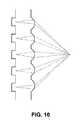
- FIG. 16is an illustration of an embodiment of two subarrays of VCSEL array devices forming circles on detectors
- FIG. 17is an illustration of an embodiment of groupings of subarrays forming a larger circle for a detector
- FIG. 18is an illustration of an embodiment of a transceiver on a submount
- FIG. 19is an illustration of an embodiment of a linear array of subarrays and an external macro lens
- FIG. 20is an illustration of an embodiment of the linear array of FIG. 17 in a switching application
- FIG. 21is an illustration of an embodiment of a non-linear laser array and a macro lens operating as a digital switching device
- FIG. 22is an illustration of an embodiment of computing or communication devices connected to digitally switched laser arrays
- FIG. 23is an illustration of an embodiment of a linear transceiver
- FIG. 24is an illustration of an embodiment of a 4 ⁇ 4 optical switch
- FIG. 25is an illustration of an embodiment of a 12 ⁇ 12 optical switch.
- FIG. 26is an illustration of an embodiment of an array of laser devices focused at different points in space.
- VCSEL array devicessuch as those described in U.S. Pat. No. 5,812,571, are flip chip VCSEL array devices that employ a metal contact layer that is also used as a reflector for the top mirrors, and which is formed over each of the mesas.
- This single metal layeris customarily deposited with techniques such as electron beam (e-beam) evaporation or sputtering in order to create a highly uniform or reflective surface.
- e-beamelectron beam
- the dissipation of heat, and the reduction of both parasitic capacitance and inductanceare achieved by reducing the common p-contact area to a minimal size and increasing the distance between the common contact pad and the substrate ground, while surrounding the common contact pad with a ground plane at a distance derived from the properties of a coplanar waveguide, and forming a raised heat sink proximate to each active mesa element and grounding mesa in the array.
- the minimized common p-contact area of the embodimentdeparts significantly from existing designs which require an extended common p-contact area in order to make contact with wire bonds.
- the embodimenteliminates the need for wire bonds.
- the elimination of wire leadsreduces inductance, while the raised height of the resulting mesas and heat sink structure increases the distance between the negative and positive potentials under electrical bias from the substrate ground to the contact pad on the heat sink substrate, thereby reducing the overall parasitic capacitance of the system. This is achieved through the use of a seed layer for formation of a thick plated metal heat sink that allows for much greater heat reduction through the edge of each VCSEL, as well as improving frequency response.
- ground (or negative) electrical connectionis contacted through shorted mesa devices bringing the current flow through a coplanar lead and to the heat spreader, or heat reducing substrate, without the use of wire bonds.
- Wire bondsare used in existing designs to connect the top of the substrate to the ground of the package and are undesirable because they introduce parasitic inductance, which has negative effects on the frequency response of VCSEL array devices.
- the numerous wire bonds required by existing designsintroduce significant manufacturing complexity, greater potential for defects, and increased costs.
- FIG. 1shows a simplified schematic cross-section of VCSEL array device 100 in accordance with an embodiment.
- the illustration of the VCSEL array device in the embodimentshows a semiconductor device array and a method of fabricating and bonding the semiconductor device array. It will be understood, however, that the method disclosed therein can be used to fabricate arrays of other semiconductor devices, such as light emitting diodes, photodetectors, edge-emitting lasers, modulators, high electron mobility transistors, resonant tunneling diodes, heterojunction bipolar transistors, quantum dot lasers and the like.
- the illustration of VCSEL array device 100 in the embodimentis for illustrative purposes only and is in no way meant to limit the scope of the invention.
- VCSEL array device 100includes a substrate 102 which includes Gallium Arsenide (GaAs), although other materials such as Indium Phosphide (InP), Indium Arsenide (InAs), Silicon (Si), an epitaxially grown material, and the like, could be used to form the substrate 102 .
- substrate 102typically includes a lattice constant chosen to minimize defects in a material layer subsequently grown thereon. It will also be understood that the choice of at least one of the compositions and the thicknesses of the subsequently grown material layers will provide a desired wavelength of operation.
- Subsequent layersare deposited on the substrate 102 via epitaxial growth using Molecular Beam Epitaxy (MBE), Metal-Organo-Chemical Vapor Deposition (MOCVD), and the like.
- MBEMolecular Beam Epitaxy
- MOCVDMetal-Organo-Chemical Vapor Deposition
- a lattice-matched lower Distributed Bragg Reflector (DBR) 104is epitaxily deposited on substrate 102 to form the first of the raised layers of the VCSEL mesas 103 and the short-circuiting/shorting/grounding mesa 105 .
- the lower DBR 104is formed from multiple layers of alternating materials with varying (a high and a low) indexes of refraction, or by periodic variation of some characteristic, such as height, of a dielectric waveguide, resulting in periodic variation in the effective refractive index in the guide. Each layer boundary causes a partial reflection of an optical wave, with the resulting combination of layers acting as a high-quality reflector at a desired wavelength of operation.
- lower DBR 104(and upper DBR 108 , as further described below) includes more than one material layer, it is illustrated in FIG. 1 as being comprised of a single layer for simplicity and ease of discussion herein.
- a portion of lower DBR 104can also be made conductive to allow an electrical contact (not shown) to be made to the VCSEL array device.
- an active region 106is epitaxily deposited on lower DBR 104 .
- active region 106comprises cladding (and/or waveguiding) layers, barrier layers, and an active material capable of emitting a substantial amount of light at a desired wavelength of operation.
- the wavelength of operationis a wavelength within a range approximately given from about 620 nm to about 1600 nm (for a GaAs substrate).
- other wavelength rangesmay be desired and will depend on the application.
- the wavelength of emissionis substantially determined according to the choice of materials used to create lower DBR 104 and upper DBR 108 , as well as the composition of the active region 106 .
- active region 106can include various light emitting structures, such as quantum dots, quantum wells, or the like.
- upper DBR 108is positioned on active region 106 , and like lower DBR 104 , is electrically conductive to allow ohmic electrical connections to be formed (not shown).
- lower DBR 104is n-doped and upper DBR 108 is p-doped, but this can be reversed, where lower DBR 104 is p-doped and upper DBR 108 is n-doped.
- electrically insulating DBRscan be employed (not shown), which utilize intra-cavity contacts and layers closer to the active region.
- an upper mirror contacting layer 109is positioned on upper DBR 108 .
- Contacting layer 109is typically heavily doped so as to facilitate ohmic electrical connection to a metal deposited on contacting layer 109 , and hence to an electrical circuit (not shown).
- contacting layer 109can be formed as part of upper DBR 108 .
- Lithography and etchingcan be used to define each of the mesas 103 and 105 and their structures stated above. This can be achieved by patterning the epitaxially-grown layers through a common photolithography step, such as coating, exposing, and developing a positive thick resist.
- the thickness of the resistcan be varied as is known in the art, depending on etch-selectivity between the resist and the epitaxial layers, and the desired mesa geometry.
- etchingis usually accomplished using a Chlorine (Cl) based dry etch plasma, such as Cl 2 :BCl 3 , but any number of gases or mixtures thereof could be used. Etching can also be accomplished by many wet etchants. Other forms of etching, such as ion milling or reactive ion beam etching and the like, can also be used. The depth of the etch is chosen to be deep enough to isolate the active regions of mesas in the array. The etch stops either on the N mirror (lower DBR 104 ), an etch stop/contact layer formed in the N mirror (lower DBR 104 ), or through the N mirror (lower DBR 104 ) into the substrate 102 . After etching to form the mesas, the remaining photoresist is removed. This can be achieved using a wet solvent clean or dry Oxygen (O 2 ) etching or a combination of both.
- Oxygen (O 2 ) etchingor a combination of both.
- a confinement region 110can also be formed within each of the mesas. Within the VCSEL mesas 103 , the confinement region 110 defines an aperture 112 for the device.
- the confinement region 110can be formed as an index guide region, a current guide region, and the like, and provides optical and/or carrier confinement to aperture 112 .
- Confinement regions 110can be formed by oxidation, ion implantation and etching. For example, an oxidation of a high
- Aluminum (Al) content layercan be achieved by timing the placement of the wafer or sample in an environment of heated Nitrogen (N 2 ) bubbled through Water (H 2 O) and injected into a furnace generally over 400° C.
- N 2Nitrogen
- H 2 OWater
- confinement region 110can include more than one material layer, but is illustrated in the embodiment as including one layer for simplicity and ease of discussion. It will also be understood that more than one confinement region can be used.
- the mesa size, and apertures of the light producing VCSELsare the same and have uniform spacing.
- the individual VCSEL mesa size for the devices in an arraycan differ.
- the VCSEL mesa spacing in the arraycan differ.
- the separation of the light producing VCSELs mesas in an array 100is between approximately 20 ⁇ m and 200 ⁇ m. However, larger and smaller separations are also possible.
- Dielectric depositioncan be used and processed to define an opening for a contact surface.
- the deposition of a dielectric material 114 over the entire surface of the device 100is usually accomplished by Plasma Enhanced Chemical Vapor Deposition (PECVD), but other techniques, such as Atomic Layer Deposition (ALD), can be used.
- PECVDPlasma Enhanced Chemical Vapor Deposition
- ALDAtomic Layer Deposition
- the dielectric coating 114is a conformal coating over the upper surface (including the mesa sidewalls) and is sufficiently thick so as to prevent current leakage through pinholes from subsequent metal layers.
- An example of this techniqueis to follow a deposition of PECVD Silicon Nitride (Si 3 N 4 ) with an E-beam deposition of Si 3 N 4 , or another dielectric could be deposited that has a more directional deposition rate, thereby putting thicker dielectric material on the incident surfaces.
- a photolithographic processis then used to define openings in the dielectric over each of the VCSELs mesas where contact is to be made to the top mirror contact layer 109 .
- the dielectric layer 114is also removed over the substrate 102 between each of the VCSEL mesas 103 , over the substrate 102 surrounding the ground mesa 105 , and over the top and side of each ground mesa 105 .
- the next processing stepis a photolithographic process that is used to define the contacts over the top mirrors 108 , where the dielectric was opened in the above step, so that a p-metal layer can be formed therein in a subsequent step.
- the opened area in the photoresistis slightly larger than the opening in the dielectric, typically of the order of a few ⁇ m wider.
- its diametercan be smaller than the diameter of the dielectric opening, or as large as the diameter of the heat sink material over the shorted mesas, which is plated at a later step. This opening could not be any larger than the mesa diameter in an active light producing mesa or the subsequent metals would short out the p- and n-potentials, unless the dielectric coating is conformal and covering the N mirror portion at the mesa base.
- the p-metal contact layer 120is usually a multilayer deposition that is deposited by E-beam, resistive evaporation, sputter, or any other metal deposition techniques.
- a thin Titanium (Ti) layeris first deposited for adhesion of the next layer.
- the thickness of this adhesion layercan vary greatly, but is generally chosen to be between about 50 ⁇ and about 400 ⁇ as the Ti films are stressful and more resistive than the subsequent layers. In an embodiment, the adhesion layer is approximately 200 ⁇ thick.
- Other adhesive metal layerscan be substituted for this layer such as Chromium (Cr), Palladium (Pd), Nickel (Ni), and the like. Also this layer can serve as a reflector layer to increase reflectance of the contacting mirror.
- the next layeris deposited directly on top of the adhesion layer without breaking vacuum during the deposition. In many cases this layer acts as a guard against the Gold (Au) or other top metals from diffusing too far into the contact (a diffusion barrier) because of excessive heating at the bonding stage.
- Metals chosenare generally Pd, Platinum (Pt), Ni, Tungsten (W), or other metals or combinations of these metals chosen for this purpose.
- the thickness chosenshould depend upon specific bonding temperatures needed in the flip chip process. The thickness of this layer is typically between about 1,000 ⁇ and about 10,000 ⁇ .
- a diffusion barrier layercan be optional, and not deposited as part of the metal contact stack.
- the next layeris generally Au but can be Pd or Pt or mixtures such as Gold Beryllium (AuBe) or Gold Zinc (AuZn).
- the thickness of this layeris approximately 2,000 ⁇ . However, it can generally have a wide range of thicknesses depending on the photo resist properties and heating characteristics of the deposition.
- another metalcan also be deposited at this time to increase metal thickness and to form the metal heat sink at this stage, thereby reducing the number of processing steps, but this technique is not necessary and was not utilized in the demonstration devices described below.
- a common liftoff techniqueis chosen for this photolithographic process so that the metal deposited on the surface can easily be separated from the areas of the surface covered with photoresist, such that any metal on the photoresist is removed without sticking to or affecting the adhesion of the metal to the semiconductor.
- a photolithographic processis then used to define the openings over various portions of the substrate 102 and the shorted n-contact mesas 105 , where the dielectric was opened in a previous step.
- the opened area in the photoresist corresponding to the n-metal depositionshould be slightly larger than the opening in the dielectric openings for the n-metal.
- N-metal layer 122is then deposited and can form an electrical circuit with the substrate 102 either through the lower DBR 104 (if an n-mirror), an etch stop and contact layer which is generally heavily doped within lower DBR 104 , or to substrate 102 itself.
- the process to form the n-metal layer 122is similar to that for the p-metal layer 120 .
- the metal layerscan be chosen to include the combinations of Ni/Ge/Au, Ge/Au/Ni/Au, or many such combinations.
- the first layer or layersare chosen to reduce contact resistance by diffusion into the n-doped epitaxial material of the substrate 102 .
- the first layer of the multi-layer metal stackcan also be chosen as a diffusion-limiting layer such as Ni so that in the annealing process the metals do not “clump” and separate due to the various diffusion properties of the materials. Evenly distributing diffusion of these metals is desired and can be used to lower the contact resistance which also reduces heating.
- the thickness of this multi-layer metal stackcan vary greatly. In the embodiment to be described, a Ni/Ge/Au metal stack with thicknesses of 400 ⁇ /280 ⁇ /2,000 ⁇ , respectively, was used.
- a Rapid Thermal Anneal (RTA) stepis then performed on the wafer in order to lower contact resistance.
- the process temperatureis rapidly ramped up to ⁇ 400° C., held for about 30 seconds and ramped down to room temperature.
- the temperature and time conditions for the RTA stepdepend on the metalization, and can be determined using a Design Of Experiment (DOE), as known to those of ordinary skill in the art.
- DOEDesign Of Experiment
- this stepcan be performed at an earlier or later stage of the process flow, but is generally done before solder is deposited so as to reduce oxidation of the solder or adhesive metal.
- a photolithographic process(using a thin layer of photoresist, typically around 1 ⁇ m to 3 ⁇ m, is used and developed to define the contact openings over the substrate 102 and shorted N contact mesas 105 , and active mesas 103 where the heat sink structures will be plated or built up.
- the next stepis deposition of the metal seed layer and is usually a multilayer deposition and deposited by E-beam, resistive evaporation, sputter or any other metal deposition techniques.
- the metal layerscan be chosen such as Ti/Au, 20 ⁇ /600 ⁇ , or many such combinations where the first layer or layers is deposited for adhesion and ease to etch off, and the second layer for conductivity and ease to etch off.
- the seed layeris continuous over the surface allowing electrical connections for plating, if this technique is used for building up the heat sinks.
- a thick metalis then deposited by plating, to form heat sink 124 .
- other methods of depositioncan also be used, in which case the metal seed layer is not required.
- a photolithographic processis used to define the openings over the openings defined with the previous seed layer resist. The photoresist is removed in the areas where the deposition will occur. The thickness of the photoresist must be chosen so that it will lift off easily after the thick metal is defined and typically ranges in thickness from about 4 ⁇ m to about 12 ⁇ m.
- a plasma clean using O 2 , or water in combination with Ammonium Hydroxide, (NH 4 OH),is performed to clear any of the resist left on the gold seed layer.
- the heat sink 124 metalis plated next by means of a standard plating procedure.
- Copper (Cu)was chosen as the metal for plating due to its thermal conductance properties, but non-oxidizing metals, such as Au, Pd, Pt, or the like, that provide good thermal conductance and provide an interface that does not degrade device reliability, could be more appropriate.
- Plating thicknessescan vary. In the embodiment described, an approximately 3 ⁇ m thickness was used.
- solder plating solutionsuch as Indium (In) plating to form a bonding layer 126 .
- Other metalscan be chosen at this step for their bonding characteristics.
- the thicknesscan vary greatly. In the embodiment described, approximately 2 ⁇ m of plated In was deposited on the heat sinks. However, other solders such as Gold Tin (AuSn) alloys can also be used, and alternative deposition techniques such as sputtering can also be used.
- the photoresistis then removed using solvents, plasma cleaned, or a combination of both, as previously described, and the seed layer is etched with a dry or wet etch that etches Au, then etched in a dry or wet etch that etches Ti and/or removes TiO 2 .
- the seed layer photoresistis then cleaned off with standard resist cleaning methods. At this point, the VCSEL array substrate is complete and ready for bonding.
- the full encasement of the mesas with a thick heat sink materialis an important aspect of the embodiment. Since the active regions of the mesas are closest to the edge where the thick heat sink material is formed, there is good thermal conductance, thereby enabling the design of the embodiment to efficiently and effectively remove heat generated by those active regions. As previously noted, this is a significant departure from existing VCSEL array device heat reduction techniques, which place the heat sink material on top of the mesa. These existing or prior designs require heat to move through a series of higher thermally conductive materials (mirrors) or dielectrics, thereby resulting in less efficient and effective heat reduction.
- mirrorsthermally conductive materials
- the dielectric layer 114covers the entire n-mirror or substrate around the mesas and is not opened so that the heat sink material can completely encompass all mesas and form one large heat sink structure, instead of individual mesas of heat sinks.
- the n-contactswould only be needed to extend from the short circuited mesas to the substrate.
- the heat sinks of the embodimentalso improve the operation of the VCSEL array by reducing the amount of heat generated by neighboring mesas. A reduction in thermal resistance within most electrical devices will increase the frequency response of each device. By improving the thermal performance of the VCSEL array device of the present device, a significant increase in the high speed performance of the VCSEL array device is made possible. Furthermore, in this embodiment it is also evident that the extra height given the mesas, because of the thickened heat sinking build up compared to the existing array circuits, reduces capacitance by increasing the distance between the substrate ground plane and the positive contact plate connecting all active mesas in parallel. The resultant effect is a reduction in parasitic impedance of the circuit which also increases the frequency response of the entire array.
- the short circuited mesa designwhich forms a sub-array surrounding the active regions, allows current flow directly from the fabricated VCSEL substrate to the ground plane on the heat spreader without the use of forming multiple wire bonds.
- This aspect of the embodimentreduces the complexity of fabrication, and also reduces parasitic inductance from the multiple wire bonds exhibited in the existing arrays.
- the short circuited mesa designwhen flipped chipped to the heat spreader substrate, forms a coplanar waveguide which is beneficial to the frequency response of the array. This design feature also enables simpler packaging designs that do not require raised wire bonds, which also impact reliability and positioning.
- a photoresistis deposited and defined over the surface of a substrate.
- a common liftoff techniqueis then chosen for the next photolithographic process so that a metal is deposited on the surface and can easily be removed from the areas of the surface covered with photoresist.
- the metal layeris then deposited with any method.
- the photoresistis cleaned off by any standard resist cleaning technique.
- the heat spreader or heat reducing substrateis ready for flip chip bonding.
- Two contact padsare then created—a first contact pad 202 for connection to the VCSEL devices 103 , and a second contact pad 204 for connection to the short circuited mesa devices 105 .
- first contact pad (or signal pad) 202is approximately circular and second contact pad (or grounding pad) 204 forms a loop around first contact pad 202 , so as to form a coplanar waveguide lead in a ground-signal-ground configuration.
- This configurationis well known for superior signal characteristics and allows flexible device testing and packaging.
- the contact pad 202can be square or another shape with the grounding pad 204 forming a loop around it, such as is shown in FIG. 3B .
- the grounding plane or loopmust have a consistent gap 206 width from the contact pad 202 to maintain the best operating characteristics, however, the rest of the ground metal can extend beyond the ring shown in FIG. 3A , and even to the edges of the substrate, as shown in FIG. 3B , for ease of grounding connections.
- the coplanar waveguidecan be designed to match impedances of the driver circuit by simply adjusting the gap width 206 and/or the signal lead width based on given metal and non-conducting substrate thicknesses and material characteristics.
- the formulas for calculating the impedance of coplanar waveguides having a dielectric substrate of finite thicknessare well known, but lengthy and are not repeated here.
- the calculated width of the gapshould be 200 ⁇ m, or 0.2 mm. More accurate calculations requiring many higher order considerations, such as current limits, hysteresis, temperature, surface characteristics and background considerations, could also be performed.
- the VCSEL array and short circuited mesa arrayare shown as dotted lines to represent where the VCSEL array and the short circuit mesa array will be bonded to the heat spreader substrate, and hence the location of both arrays after bonding.
- the bonding depositioncan also be formed on the heat spreader substrate 200 at these locations.
- the laser emissionis then directed through the mirror 104 and on through the substrate 102 forming a multibeam array.
- the substrate thicknessis reduced in order to reduce optical power losses resulting from substrate transmission characteristics.
- FIG. 4shows an alignment of VCSEL array 100 with substrate 200 , prior to bonding.
- the bonding processis accomplished by a machine that aligns the two substrates together, then places them in contact with each other and heats one or both substrates either before or after contacting said substrates.
- the bottom substratewas heated to about 285° C. and held at that temperature for about 10 min.
- a 20 gram weightwas used on the downward substrate position.
- the bonded waferswere allowed to cool to room temperature, finishing their processing.
- the substrate 102can be removed from the mirrors 104 by adding a selectively etched layer such as a layer of Aluminum Gallium Arsenide (AlGaAs) ( ⁇ 98%, Al), with a high Aluminum (Al) content or the like, or a layer composed of Indium Gallium Phosphide (InGaP), or other such selective materials that will etch at greatly different rates than the Galium Arsenide (GaAs) substrate.
- This layeris grown in the epi growth between substrate 102 and the first epi deposition of mirror 104 .
- an under fill of materialsuch as resist or epoxy, is used to protect the device fabrication features.
- etchconsisting of mostly Hydrogen Peroxide (H 2 O 2 ) with a small amount of Ammonium Hydroxide (NH 4 OH) can be used to quickly etch off the substrate leaving the etch selective layer, as the etch will not attack it or the etch rate slows down drastically.
- the etch layercan be selectively removed without damaging the surface of the material under it by etching the layer in a Hydrochloric acid (Hcl) solution.
- HclHydrochloric acid
- a low resistive contact layeris also grown as a first layer for formation of an n-contact layer as part of mirror 104 . After the substrate and selective etch layers have been removed, contacts can be formed on the surface of 104 and circuits can also be formed with common photolithography steps described above.
- the mesasare etched to the substrate, this process could separate each of the VCSEL elements and short circuited mesas from each other, which would benefit the VCSEL array by removing the Coefficient of Thermal Expansion (CTE) associated with the substrate.
- CTEis a physical property of materials expressed as the amount of expansion of the material per degrees Celsius. Many times, when multiple materials are used to build devices and the CTEs of those materials do not closely match, stresses can be produced within the device with any temperature changes. With the mesa devices etched to the substrate, the devices will expand at the same rate as the heat sink substrate, except over the much smaller area of where the contacts to the heat sink substrate are formed.
- the etch process used to remove the substratecould use plasma based chemistry instead of the chemical wet etch technique described above.
- the above described process flowis given by way of example only. It will be understood that switching the order of some of the steps described is possible, for example the order of the metal depositions, or depositing one or both of the n-metal or p-metal before the oxidation step. Also, it is possible to replace the top mirror structure 108 with a dielectric DBR stack, or replace the mirror stacks either entirely or partially by etching gratings on the top surfaces of the mesas.
- the gratingsare usually defined by e-beam lithography instead of photolithography and then dry etched to a specific depth. This reflects the light back with a higher efficiency and is possibly less costly than the epitaxially grown mirror or portion of mirror it replaces.
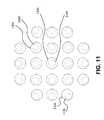
- FIG. 5An example of an array formed in a similar manner and shape is illustrated by FIG. 5 .
- Each of the single VCSEL devices (represented by solid circles in FIG. 5 ) in the VCSEL arrayare electrically connected in parallel to form a single high-power, high-speed light source.
- the parallel configuration for both signal and ground pathsreduces the series resistance and inductance of the flip-chipped array.
- the arrayused 28 active light producing mesas, evenly spaced apart. They were formed in a circular pattern and the entire area of the active region (contact pad) was less than 0.2 mm 2 . There were 18 shorted mesas (which are similar to those represented by dashed circles in FIG. 5 of the larger array device) in the grounding ring that surrounds the circular pattern of VCSEL devices.
- the lasers (and arrays) of the tested deviceswere fabricated from layers grown using Molecular Beam Epitaxy (MBE) deposited on an n-type GaAs substrate.
- MBEMolecular Beam Epitaxy
- the light producing portion of the active region 106 in the device of FIG. 1contains three Indium Gallium Arsenide (In0.18Ga0.82As) quantum wells.
- This VCSEL designemploys a gain mode offset, which occurs when the wavelength design of the active region is not the same as the wavelength design of the mirrors at room temperature. When the device heats up, the emission wavelength from the active area will shift a specific amount per degree Celsius. A gain mode offset takes this shift into account, so when the mirrors are designed they match the emission wavelength at an elevated temperature.
- a gain-mode offset designis well suited for high temperature operation of the array at high bias currents. However, smaller offsets would enhance the modulation response at low temperatures and a lower reflectivity bottom mirror 104 would increase output power.
- the fabrication of this device with the processes mentioned abovereduced thermal resistance down to 425° C./W for a single mesa identical to those used as elements in this array.
- FIG. 6shows the Light-current (I)-Voltage (L-I-V) characteristics of an exemplary array.
- the threshold current and voltageare 40 mA and 1.7V respectively.
- the dashed circles over the two linesindicate the sides of the chart each of the lines represent so the units can be read properly.
- the Continuous Wave (CW) output power of the arrayis above 120 mW at 500 mA bias current and room temperature.
- FIG. 7shows the modulation responses for selected bias currents at 20° C.
- the arrayexhibits a 3 dB frequency of 7.5 GHz at a 500 mA bias current. Cut off frequency of the high current Picosecond Pulse Labs bias tee employed here presents accurate measurements below 1 GHz. The bandwidth can be extended to higher frequencies by increasing the bias current. Frequency response measurements for a single 18 ⁇ m active diameter laser nominally identical to those constituting the test array show that a 3 dB modulation frequency of up to and above 10 GHz is achievable.
- FIG. 8shows that the frequency response of elements of the array at different radii measured from the center of the array is nearly independent of position. Each point indicates the frequency response of an individual device in the array. This result indicates that both the individual laser performance and current distribution are relatively uniform over the entire array.
- VCSEL arrays in accordance with the embodimentcan be scaled up to hundreds or thousands of elements to achieve watt level CW powers with modulation frequencies approaching 10 GHz.
- VCSEL arrays of this typeare expected to be useful for moderate range, high resolution LIDAR and free-space communication, as well as numerous other applications.
- FIG. 9shows a pulsed response of an exemplary array with a 50 ps pulse at FWHM (Full Width at Half Max), which indicates the width of the pulse at half of its maximum power.
- the lines of the chartrepresent 40 ps divisions.
- microlensesmay be fabricated on the backside of the surface of substrate 102 by using a number of different processes.
- One technique for forming such microlensesinvolves a photolithography process that defines the lens with photoresist, such as in the form of cylinders or other shapes, and then melts the photoresist onto the substrate before transferring those lens shapes to the substrate through an etch.
- the etchmay be a Chlorine (Cl) based dry etch adjusted for or approaching an even etch selectivity between the substrate material and the photoresist, so as to etch both materials at close to or at the same rate.
- the photolithographic step used to create the lensesis accomplished using a backside wafer alignment system common in the industry. This step would be fabricated either at the end of fabrication of the VCSEL wafer or earlier, but generally before the flip chip process described above.
- Other processes that may be used to form the lensesinclude gray scale lithography, where a partially transmissive photomask may be used to produce relief profiles in the photoresist.
- the resulting lensesmay allow a gradually changing amount of light through different parts of the lens, such as allowing more light to pass around the edges and less light to pass at the center, or vice versa.
- Various direct write lithography processesmay also be used to define a surface profile for a polymer resist coating. Small amounts of polymer materials may also be deposited on the surface of the substrate above each laser device that form lenses as the polymer cures, such as commonly deposited epoxy from inkjets.
- the microlensesmay be fabricated on a separate transparent substrate that is attached and aligned to the laser array.
- the substrate material usedmay be any material transparent to the laser wavelength. It may be formed by injection molding, casting, hot pressing or direct machining processes. The same strategy of offsetting microlenses from the optical axis of each emitter may be used with separate microlens arrays.
- the profiles of the microlenses fabricated as described hereinmay be simple, such as the hemispherical lenses illustrated in FIGS. 10 and 11 , or more complex, such as aspheric profiles that can be used for extended depth of field applications. In the case of hemispheric lenses, it may also be possible to control an aspheric profile.
- Other complex optics that may be formedinclude holographic optics that direct the beam in a variety of directions or diffractive optics that split the beam generated by a laser device into sub-beams, each potentially pointed in a slightly different direction.
- the opticscan have various patterns formed on a surface that may be useful for forming highly astigmatic beam profiles.
- opticsmay be formed or patterned so as to alter or control polarization.
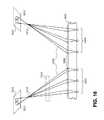
- each lenscan be offset by a desired amount to cause what would otherwise be a spread of parallel beams of light emitted by the VCSEL array to be focused into a selected pattern, such as on a tightly focused spot (as previously noted, the distance from the lenses to the beam convergence point of FIG. 10 is not drawn to scale).
- FIG. 10 and 11further illustrate how the lens 1100 (represented by a solid circle) for the centered VCSEL device 1102 (represented by a dashed circle) is centered over that VCSEL device 1102 , but the lenses 1104 for the other VCSEL devices 1106 outside of the centered VCSEL device 1102 are positioned at a specified offset distance from the centered VCSEL device 1102 so that light passing through those lenses 1104 is directed to a central point.
- the manner in which a group of lenses might be offset positioned over an array of VCSEL devicesis further illustrated in FIG. 11 .
- the integrated microlenses described aboveenable the VCSEL devices to be utilized in short-range free-space optical links that do not require external collimating or collecting optics. This, in turn, enables extremely compact system designs that can be used in thin-profile mobile electronic systems in place of near field RF technologies.
- an array of VCSELscan produce a convergent array of beams as described above. For short distances, a few millimeters at most, the convergent beams can efficiently fill a high-speed detector without the need of an external collecting optic.
- This schemeis ideally suited for free space optical communication between two devices that are brought into contact or near contact (a few millimeters at most) and where an IR-transmissive housing or window is provided.
- Mechanical alignmentcan be facilitated by kinematic features on the devices.
- further alignmentcan be performed by actively selecting subarrays (within the VCSEL array) having associated microlenses that direct light into adjacent areas. For example, when the optical link is established, the most efficiently coupled subarray of emitters may be used while the other subarrays may be dormant. The initial link may use all of the subarrays at first until feedback from the link is established, at which time some of the subarrays may be turned off, which may conserve power and extend battery life of mobile devices.
- the detectordoes not need a collection optic to concentrate the beam down to a small spot as this is provided by the microlenses.
- the size of the spot and the distance of the beam convergence from the lens surfacemay be determined by a number of factors, including the lens curvature, degree of offset of the lens from the laser emitter axis, index of refraction of the lens material, and the modal characteristics of the lasers. If the microlenses are aligned axially with the laser emitters (as illustrated in FIG. 11 ), the beams may be focused, collimated or be more divergent, depending on the radius of curvature of the lens and the distance (defined by the substrate thickness) to the source.
- the beamwill be directed at an angle to the axis. This is equivalent optically to an object at a given field height being imaged at an off axis position in the image plane. In combination with the focusing effect of the lens, this gives the designer a variety of options in transforming the beam properties of each element of the array. Again, a simple example is the creation of a converging set of beams that overlap at a specific distance from the surface of the lenses. If each lens in the array is offset from the axis with the amount of offset dependent on the distance of the laser array element from the axis, the beams can be made to converge at a single point (as illustrated in FIG.
- This approach to creating a focused beam spot without a large focusing lensmay have other applications besides short range free space optical communication. It may be used for concentrating a beam for materials modification, injecting light into optical fibers and waveguides, optical pumping of solid state and fiber lasers, medical treatments of a specific volume of tissue or location on the skin or other bodily surface or membrane.
- the beam of each lasercan be deflected at an angle and focused or defocused, as illustrated in FIG. 10 , depending on the microlens design and spacing from the emitter. This allows the designer to converge the beams with a pattern of microlenses with different offsets.
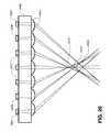
- This control of the beam direction and focusingallows for the direction of the laser light into a single spot ( FIG. 10 ) where a detector is positioned to receive the signal, but other focusing arrangements are also possible, such as illustrated in FIG. 12 , where the focal spot is a virtual focus (which may also act as a virtual source of other optical systems) 1200 located behind the array 1202 of VCSEL devices 1203 .
- an additional external lens 1204is also illustrated to show that it is possible to combine the microlens array with other optical systems to achieve other effects, such as the collimated beams of light 1206 from the array 1202 .
- embodiments described hereinmay use a submount to make electrical contact to the laser array (through flip-chip bonding) and the elements of the array may be contacted with a solder ball or other conductive bond to a submount that provides mechanical support, electrical contact and thermal conduction.
- FIG. 13depicts a laser array 1300 flip-chip bonded to a submount 1302 .
- the lasers(not shown) are located on the bottom surface of the array 1300 and project their light through the thickness of the substrate of the laser array 1300 and through the pad 1304 .
- the lasers of the laser array 1300are electrically bonded to an electrical contact (not shown) at the end of the impedance matching transmission line 1306 , which is positioned under the laser array 1300 .
- the transmission line 1306provides for transmission of high data rate optical signals to the laser array 1300 .
- the microlenses 1308are illustrated by the individual circles on the pad 1304 of the substrate of the laser array 1300 .
- the submount 1302may be formed of many possible materials, including silicon, ceramic, printed circuit boards and flat-flex cables.
- the microlens structure described hereinwhen used in free space optical applications, is referred to as a “lensless” free space optical link because the combined laser array and microlens structure does not require the addition of typical, large collimating and collecting lenses.
- a lensless linkalso offers unique alignment techniques that may not be possible with more traditional technology.
- the alignment of the transmitting laser beam to the receiving detectoris a critical parameter in whether or not the link between the two will be successful. For mobile device applications, this is an especially big problem.
- a fixed link with no active scanning or alignment adjustmentwill be difficult to line up, even over very short distances. While the alignment tolerances may be reduced by making the beam spot bigger, this technique is limited by the resulting increased power consumption.
- active mechanical scanning or tracking of the transceiverstends to be too bulky and expensive to justify implementation.
- embodiments described hereinmay use a multi-element laser array 1400 with the laser emitters (not shown, but located on the bottom of the array 1400 as illustrated) being subdivided into a number of subarrays 1402 shown within the pad 1404 of the substrate.
- the use of subarrays 1402adds an active alignment element to any mechanical alignment solutions.
- each subarray 1402may be configured to illuminate a specific region of a volume defined by the combined mechanical tolerances.
- the corresponding subarray 1402may be activated and the resulting laser beams directed by the microlenses 1406 lined up with those array elements will define the output of the array.
- the submount 1408may include a separate transmission lines 1409 , 1410 , 1411 and 1412 connected to separate contact pads 1413 for each subarray 1402 .
- the individual laserscould be connected to separate electrical contacts and transmission lines that would enable each of the individual lasers to be driven separately.
- each subarraymay be similarly turned on by a control circuit associated with the driver electronics for the array.
- Subarrays and individual VCSEL devicescan also be controlled by a controller other than the driver, such that the driver is under the control of that controller.
- any combination of the subarraysmay be turned on individually or in combination within the capability of the addressing and driver electronics.
- the array 1400may be configured for a linear scanning or 2D scanning capability and may direct the output to different detectors if that is desired, as further discussed below. This allows for a non-mechanical beam scanning capability.
- the scanningmay be a discrete point to point addressing by the optical beams, or may look more like continuous scanning by a larger number of subarrays with microlenses arranged so that small incremental changes in beam position occur with switching from one subarray to another. While the subarray approach adds array elements, the packing density is high and the increased size of the die is a modest expense for the added system functionality.
- the size of the array and the number of subarraysmay be determined mostly by the tolerances to be covered. The tolerances not only include the alignment of the two system housings to each other, but also the internal variation in the position of the circuit boards within the assembly modules. If the transmitter and receiver are on separate modules within the assembly, there may be tolerances around those assemblies and the fit of those assemblies in whatever kinematic constraints are fabricated into the parts.
- FIG. 16is a cross-sectional view illustrating an embodiment of a VCSEL array 1600 with two subarrays or subgroups 1602 and 1604 .
- Subgroups 1602 and 1604includes a number of corresponding microlens 1606 that are offset in a particular manor so as to direct their beams 1608 and converge those beams 1608 to form circles or blur circles 1610 around the detectors 1612 .
- the circles 1610are referred to as “blur circles” as they are formed behind the focal point 1614 of the offset subgroups 1602 and 1604 .
- the blur circles 1610are the area of the beams' 1608 expansion and correlate to where the power density of the beams 1608 is sufficient to enable a particular bandwidth.
- an optical element 1616such as a holographic optical element, may be positioned somewhere in the path of the beams 1608 in order to homogenize the beams 1608 , which serves to reduce bright spots and spread the power in the beams 1608 more evenly.
- the subgroups 1602 and 1604may be formed so the beams 1608 are specifically directed at a detector or groups of detectors so as to form the basis of an optical router.
- FIG. 17is an embodiment of a grouping of multiple subgroups 1700 of an array 1702 , with the subgroups 1700 arrayed about a central area, with the exterior subgroups 1700 having a separate converging point for the beams 1704 and where all exterior points are encircling the central subgroup convergence point 1706 .
- This embodimentillustrates a configuration that may form an overlapping of the beams 1704 so that they cover a much larger area 1706 than may be possible with a single VCSEL beam or a single subgroup of VCSEL devices.
- the configuration illustrated in FIG. 17may be used by turning on each subgroup in sequence until a return is gathered from a receiver, which in turn identifies which subgroup is best aligned with the detector.
- all other subgrouped arraysmay be powered down to conserve energy and reduce heat build-up.
- Many other schemesmay be likewise employed to identify the subarray 1700 with the best alignment, such as turning all of the subarrays 1700 on, then turning the subarrays 1700 off one at a time. This embodiment may be useful in lower power applications and to increase angular alignment tolerances.
- the active alignment process for a free space optical linkmay include initially powering up the subarrays 1402 in sequence and determining which subarray 1402 is best able to sustain the link.
- the control for this processmay be provided by the host system. If latency from sequential implementation of the link is too long, the arrays may be powered up together initially and then sequentially powered down while the link is running to optimize the link efficiency.
- control systemmay then periodically re-optimize the link. Given that a subarray 1402 has to be run at a multiple of the threshold current, it may not be optimum to split power between the subarrays, so the sub-volumes of the tolerance box may need to be carefully partitioned between the subarrays 1402 .
- a subarray used to address a given zone within the tolerance boxmay have separately contacted elements within it that can be powered on or off to adjust the transmit power.
- Thismay have advantages for the control electronics as the selection of the subarrays is a digital switching function as opposed to analog control of the drive current to the lasers. This has some advantages in simplifying the driver electronics. It also allows the arrays to be driven at optimum current levels to maintain high data rates and modulation efficiencies. VCSELs are difficult to modulate at high speed if the current is too close to threshold.
- the driver for the laser arraymay include eye-safety circuitry such as that described in co-pending application Ser. No. 13/868,034, the contents of which is incorporated herein by reference in its entirety, and of which the present application is a continuation-in-part.
- an addressable laser array having multiple optical sourcessuch as individual laser devices or subarrays of such devices
- an electrical circuitso that different combinations of the optical sources can be energized without exceeding eye-safety limits and without requiring monitoring or a feedback loop to control the distance of an observer.
- Operation of the multiple optical sourcesmay be proximate, which is eye-safe, regardless of the number of or which ones of the optical sources are energized and regardless of the position of observers.
- a laser array with multiple optical sourcesmay also remain eye-safe when there are single-point electrical failures, such as short circuits, in the driving circuit.
- the scanning capability of the laser arrays described hereincan be used to track a receiver that is moving or vibrating in relation to the transmitter with feedback from the receiver than can be sent through the optical link or through a separate channel, which may or may not be optical. It can be used to address individual elements in an array of detectors or an array of optical fibers that act as receivers for detectors or other functions coupled to the other end of the fibers.
- a transceiver implementationmay be assembled as a hybrid circuit with the transmitter and receiver elements bonded to a substrate by standard hybrid packaging techniques.
- FIG. 18shows an embodiment of a transceiver 1800 built on a circuit 1802 . The components shown can be bonded to the surface by chip-on-board or by traditional hybrid assembly methods.
- FIG. 18shows the laser array 1808 on a separate submount 1806 .
- the laser arraymay also be flip-chip bonded directly to the surface of the printed circuit.
- the small laser arraymay be configured to have a slowly converging set of beams directed by offset microlenses to overlap the beams at a spot a few millimeters from the transceiver 1800 . This is sufficient distance to link two mobile devices that are touching at an edge or surface.
- FIG. 18shows a single transceiver, having a transmitter 1808 and receiver 1810 .
- the transceiverscan bridge a short distance between them through IR-transmissive plastic windows that are in contact or in close proximity.
- Various meansmay be used to ensure the surfaces are in contact with some misalignment tolerance limited by kinematic features or other constraints.
- one or more laser arraysconfigured with or without subarrays and with or without microlenses to direct the beams from the arrays/subarrays to detectors may be utilized in a digital switching embodiment.
- a linear array of subarray of laser devices 1902generate beams 1904 from the subarrays that are directed by the external macro lens 1906 (which is shown as a cylinder lens, but could be any of a number of other optical elements, such as a spherical lens).
- the angle of the beamsis shown at angles that may not be realistic givens the physical arrangement of the laser devices 1902 and the optical element 1906 .
- the same array 1900 and macro lens 1906(which may likewise be a different optical element) are depicted in FIG. 20 to illustrate how the linear array 1900 could be used in a switching application, where selective operation of the laser devices 1902 and the arrangement of the optics/macro lens 1906 serve to direct the beams 1904 to detectors 1908 for fiber optic cables 1910 arranged in a mounting structure 1912 .
- FIG. 21illustrates a further embodiment where a larger non-linear laser array 2100 (which may have a variety of configurations or laser devices or subarrays) and an optics or macro lens 2102 (driven by a driver device and/or controller not shown) are depicted operating as a digital switching device for use with the bank of detectors 2104 for the fiber optic cables 2106 of the structure 2108 . While macro lens are illustrated in FIGS. 19-21 directing the beams to locations, other optical elements, such as offset microlens, could be used to achieve the same effect, and combinations of microlenses and optical elements could be used as well.
- FIG. 22illustrates a further embodiment wherein three or more racks 2200 of computing or communication devices are connected to digitally switched laser arrays 2202 (transceiver type configurations) that transmit and receive data from and to the devices.
- each rackis a plurality of microlens equipped laser arrays on various components directing data carrying beams of light to various detectors that collect the data and further transmit that data away from the racks 2200 , which detectors likewise receive data being transmitted to the racks 2200 .
- FIGS. 23-25Additional embodiments of transceivers are illustrated in FIGS. 23-25 .
- a configurationis illustrated where each switching element 2302 of a transceiver switch 2300 consists of four detectors 2304 and four transmitters 2306 .
- a transceiver switch 2402consisting of four switching elements 2302 , may be configured to communicate with an opposing transceiver switch 2404 , likewise consisting of four transceiver switching elements 2302 .
- the beams 2406 of each subgroup of transmittersare directed toward a specific detector of the other set of transceivers.
- FIG. 25illustrates one of a number of configurations of this optical switch, in this case as a 12 ⁇ 12 optical switch 2500 .
- arrayed subgroupsdirecting beams to detectors, and the reverse, thereby allowing communication between boards, circuits, processors, switches, and the like.
- arrayed VCSEL devices and subgroups or subarraysthat may be used for other purposes, aside from free space communication.
- the individual VCSEL devices or subarrays of a VCSEL arraydo not all have to be focused on the same focal spot.
- a linear array 2600 of VCSEL devicesmay be focused, through utilization of the microlenses 2602 on more than one focal spot. As shown in FIG.
- sets of devicesmay be focused on different common focal spots, such as the two outer devices 2604 being focused on spot 2606 , the next two devices 2608 being focused on spot 2610 , and the three interior devices 2612 being focused on spot 2614 .
- Focal spots 2606 , 2610 and 2614would effectively form a line in space, which may be useful for use of the laser device as a cutting tool, such as a surgical scalpel.
- VCSEL devices/subarrays and microlens structuresmay also be shaped and focused to create other shapes aside from a line, such as a circle of focal spots and other geometric patterns for other purposes.
- the array 2600 of FIG. 26could be used for the medical devices noted, but could also be used in the marking of materials by using known techniques, such as a x-y plotter type controller, to mark metal, glass, wood, etc.
Landscapes
- Physics & Mathematics (AREA)
- Electromagnetism (AREA)
- Condensed Matter Physics & Semiconductors (AREA)
- General Physics & Mathematics (AREA)
- Optics & Photonics (AREA)
- Engineering & Computer Science (AREA)
- Computer Networks & Wireless Communication (AREA)
- Signal Processing (AREA)
- Optical Communication System (AREA)
- Semiconductor Lasers (AREA)
Abstract
Description
- This is a continuation-in-part application taking priority from U.S. patent application Ser. No. 13/077,769, filed Mar. 31, 2011, entitled “Multibeam Arrays of Optoelectronic Devices for High Frequency Operation,” which is a continuation application taking priority from U.S. patent application Ser. No. 12/707,657, filed Feb. 17, 2010, now U.S. Pat. No. 7,949,024, entitled “Multibeam Arrays of Optoelectronic Devices for High Frequency Operation,” which takes priority from Provisional U.S. Patent Application No. 61/153,190, filed Feb. 17, 2009, entitled “Multibeam Arrays of Optoelectronic Devices for High Frequency Operation,” the contents of which are incorporated herein by reference in its entirety.
- This is a continuation-in-part application taking priority from application Ser. No. 13/868,034, filed Apr. 22, 2013, entitled “Addressable Illuminator with Eye-Safety Circuitry,” which claims benefit under 35 U.S.C. §119(e) of Provisional U.S. Patent Application No. 61/636,570, filed Apr. 20, 2012, entitled “Addressable Illuminator with Eye-Safety Circuitry,” the contents of which are incorporated herein by reference in its entirety.
- Semiconductor devices and, more particularly, to microlens structures for multibeam arrays of photonic devices for high power and high frequency applications, and methods of making and using the same.
- Semiconductor lasers have gained influence in high power laser applications because of their higher efficiency, advantages in Size, Weight And Power (SWAP) and their lower cost over other forms of high power lasers. Many laser applications such as industrial cutting and welding, Laser Detection and Ranging (LADAR), medical engineering, aviation defense, optically pumping rare earth doped fiber lasers, optically pumping solid state crystals in Diode Pumped Solid State lasers (DPSS), fiber-optic communication, and fusion research, among others, require a high power and high frequency response. Due to their high power array outputs, edge-emitting semiconductor lasers are widely used in such applications. However, degradation of these edge-emitting lasers is common, primarily as a result of Catastrophic Optical Damage (COD) that occurs due to high optical power density at the exposed emission facet.
- Vertical-Cavity Surface-Emitting Lasers (VCSELs), in comparison, are not subject to COD because the gain region is embedded in the epitaxial structure and is therefore not exposed to the outside environment. Also, the optical waveguide associated with the edge-emitter junction has a relatively small area, resulting in significantly higher power densities compared to VCSELs. The practical result is that VCSELs can have lower failure rates than typical edge-emitting lasers.
- To date, VCSELs have been more commonly used in data and telecommunications applications, which require higher frequency modulation, but not as much power. VCSELs have offered advantages over edge-emitting LASERs in this type of application, including ease of manufacture, higher reliability, and better high frequency modulation characteristics. Arrays of VCSELs can also be manufactured much more cost efficiently than edge-emitting laser arrays. However, with existing VCSEL designs, as the area of the array grows the frequency response has been penalized by heating complexities arising from the multi-element designs, parasitic impedances, and the frequency response of the wire bonds or leads required by the high current. Thus, the modulation frequency of the array decreases.
- VCSELs and methods for manufacturing them are known. See, for example, U.S. Pat. Nos. 5,359,618 and 5,164,949, which are incorporated herein by reference. Forming VCSELs into two-dimensional arrays for data displays is also known. See U.S. Pat. Nos. 5,325,386 and 5,073,041, which are incorporated herein by reference. Flip-chip multibeam VCSEL arrays for higher output power have been mentioned, in particular, in U.S. Pat. No. 5,812,571, which are incorporated herein by reference.
- However, VCSEL arrays that provide both high frequency modulation and high power have not been adequately developed. Furthermore, arraying such devices together increases heat generation, adding to the negative effects on high frequency operation.
- In addition, free space optical links that are intended for short range mobile device communication are generally designed with optical elements for efficient transmission of a low divergence beam (using a collimating optic) and for efficient reception of the incident light (using a collecting lens). Since high speed detectors are very small, around 60 μm in diameter for 5-10 Gb/s speeds, the collecting optic has to focus the light down to a small spot to get a good signal-to-noise ratio. Such systems are therefore very alignment sensitive, as the small spot can easily miss the small detector if something moves or perturbs the alignment. This has made free space optical communication between mobile devices difficult. The exception has been the IrDA (Infrared Data Association) standard which uses LED-based transmission into a very broad transmission beam and a hemispherical collection optic. While free space optical links were popular for a while at relatively low speeds, as mobile device concepts have evolved, a need has arisen for high bandwidth communication between two devices that can actually be touching each other or separated by just a few millimeters. There are radio frequency approaches that will work in these near field ranges, but they have disadvantages, including omnidirectional transmission which is a security concern and regulatory issues due to RF interference concerns.
- An embodiment is directed to a multibeam optoelectronic device, referred to as a VCSEL array device, which has high power and a high frequency response and various microlens structures that may be formed thereon, as well as various methods for utilization of the same. The VCSEL array device is a monolithic array of VCSELs comprised of two or more VCSELs and an array of short-circuited mesa devices. The VCSELs of the VCSEL array can be spaced symmetrically or asymmetrically, spaced according to a mathematical function for improving a power or speed characteristic, or positioned for phase relationships next to each other in an electrically parallel circuit. The VCSELs of the VCSEL array are electrically connected to a first metal contact pad formed on a heat-spreading substrate or carrier. The array of short-circuited mesa devices is formed alongside the VCSEL array and the devices are bonded to a second metal contact pad on the heat spreading substrate or carrier. These mesa devices form a short circuit from the substrate ground to the second metal contact. Each VCSEL of the VCSEL array is encompassed by a metal heat sink structure, which increases the height of each VCSEL mesa, the heat sink structure and the solder. The relationship between the heat sink structure, the VCSEL array and the mesa device array reduces the parasitic impedance characteristics of the VCSEL array device, thereby increasing its output power and increasing its high frequency response. The VCSEL array and short-circuit mesa device array can also be positioned to form a coplanar waveguide lead in a ground-signal-ground configuration in the bonded optoelectronic device. This configuration provides superior signal modulation characteristics. Microlenses may be formed on the individual VCSEL devices of the array using a variety of techniques. The microlenses may be structured and/or patterned to achieve a number of effects with the output laser light not otherwise achievable with exterior lenses.
- The drawings are provided to illustrate example embodiments described herein and are not intended to limit the scope of the disclosure.
FIG. 1 is a simplified cross-sectional view illustrating the mesa structures of both the VCSEL devices and the shorting mesa devices, including dielectric deposition, metal deposition, and oxidation structures, among others features in accordance with an embodiment;FIG. 2 is another simplified cross-sectional view of the VCSEL devices and the shorting mesa devices, further illustrating heat sinks, bonding layers, and other features in accordance with an embodiment;FIG. 3A is a top plan view of a patterned heat spreading substrate illustrating the coplanar waveguide formed from the encircling grounding plane, the signal lead to ground plane gap separation, and the signal lead in accordance with an embodiment;FIG. 3B is an embodiment of the coplanar waveguide forFIG. 3A with the grounding plane extending to the edges of the heat sink and forming a loop around the contact pad of VCSEL devices;FIG. 4 is a cross-section view of the VCSEL array device ofFIG. 2 and the heat spreading substrate ofFIG. 3A prior to bonding;FIG. 5 is an illustration of an embodiment of a VCSEL array device after plating;FIG. 6 is a graph showing L-I-V characteristics of an embodiment of a VCSEL array device;FIG. 7 is a graph showing modulation frequency for an embodiment of a VCSEL array device;FIG. 8 is a graph showing laser modulation frequency for different array positions at 450 mA bias current for an embodiment of a VCSEL array device;FIG. 9 is a graph showing pulse width from an embodiment of a VCSEL array device;FIG. 10 is a partially-broken, cross-section view of a plurality of lenses positioned on top of a VCSEL array device in accordance with an embodiment;FIG. 11 is an illustration of the manner in which each lens of the plurality of lenses is placed in an offset position over each VCSEL device of the VCSEL array device;FIG. 12 is an illustration of an embodiment of microlenses having a focal spot located behind the VCSEL array device;FIG. 13 is an illustration of an embodiment of a VCSEL array device flip-chip bonded to a submount;FIG. 14 is an illustration of an embodiment of a VCSEL array device with subarrays flip-chip bonded to a submount;FIG. 15 is an illustration of the electrical contacts and transmission lines of the submount ofFIG. 14 ;FIG. 16 is an illustration of an embodiment of two subarrays of VCSEL array devices forming circles on detectors;FIG. 17 is an illustration of an embodiment of groupings of subarrays forming a larger circle for a detector;FIG. 18 is an illustration of an embodiment of a transceiver on a submount;FIG. 19 is an illustration of an embodiment of a linear array of subarrays and an external macro lens;FIG. 20 is an illustration of an embodiment of the linear array ofFIG. 17 in a switching application;FIG. 21 is an illustration of an embodiment of a non-linear laser array and a macro lens operating as a digital switching device;FIG. 22 is an illustration of an embodiment of computing or communication devices connected to digitally switched laser arrays;FIG. 23 is an illustration of an embodiment of a linear transceiver;FIG. 24 is an illustration of an embodiment of a 4×4 optical switch;FIG. 25 is an illustration of an embodiment of a 12×12 optical switch; andFIG. 26 is an illustration of an embodiment of an array of laser devices focused at different points in space.- VCSEL array devices, such as those described in U.S. Pat. No. 5,812,571, are flip chip VCSEL array devices that employ a metal contact layer that is also used as a reflector for the top mirrors, and which is formed over each of the mesas. This single metal layer is customarily deposited with techniques such as electron beam (e-beam) evaporation or sputtering in order to create a highly uniform or reflective surface. Although these deposition techniques are normal for the stated application, they are not appropriate when seeking to achieve a thick metal layer encompassing the mesa, which is crucial for improved heat reduction in such devices. In order to use existing techniques to deposit a sufficiently thick layer, a large amount of metal must be used, such as Gold (Au), which significantly raises the cost of such devices. This type of design, and the design of other existing VCSEL array devices, also raises the overall impedance of the system and complicates heat management, thereby limiting the power and speed obtainable by such arrays.
- In an embodiment described herein, the dissipation of heat, and the reduction of both parasitic capacitance and inductance (collectively referred to herein as a “reduction in parasitic impedance”) from an optical semiconductor device array are achieved by reducing the common p-contact area to a minimal size and increasing the distance between the common contact pad and the substrate ground, while surrounding the common contact pad with a ground plane at a distance derived from the properties of a coplanar waveguide, and forming a raised heat sink proximate to each active mesa element and grounding mesa in the array. The minimized common p-contact area of the embodiment departs significantly from existing designs which require an extended common p-contact area in order to make contact with wire bonds. The embodiment eliminates the need for wire bonds. The elimination of wire leads reduces inductance, while the raised height of the resulting mesas and heat sink structure increases the distance between the negative and positive potentials under electrical bias from the substrate ground to the contact pad on the heat sink substrate, thereby reducing the overall parasitic capacitance of the system. This is achieved through the use of a seed layer for formation of a thick plated metal heat sink that allows for much greater heat reduction through the edge of each VCSEL, as well as improving frequency response.
- Additionally, the ground (or negative) electrical connection is contacted through shorted mesa devices bringing the current flow through a coplanar lead and to the heat spreader, or heat reducing substrate, without the use of wire bonds. Wire bonds are used in existing designs to connect the top of the substrate to the ground of the package and are undesirable because they introduce parasitic inductance, which has negative effects on the frequency response of VCSEL array devices. Furthermore, the numerous wire bonds required by existing designs introduce significant manufacturing complexity, greater potential for defects, and increased costs.
FIG. 1 shows a simplified schematic cross-section ofVCSEL array device 100 in accordance with an embodiment. It will be understood that the illustration of the VCSEL array device in the embodiment shows a semiconductor device array and a method of fabricating and bonding the semiconductor device array. It will be understood, however, that the method disclosed therein can be used to fabricate arrays of other semiconductor devices, such as light emitting diodes, photodetectors, edge-emitting lasers, modulators, high electron mobility transistors, resonant tunneling diodes, heterojunction bipolar transistors, quantum dot lasers and the like. Further, it will be understood that the illustration ofVCSEL array device 100 in the embodiment is for illustrative purposes only and is in no way meant to limit the scope of the invention.- In the embodiment,
VCSEL array device 100 includes asubstrate 102 which includes Gallium Arsenide (GaAs), although other materials such as Indium Phosphide (InP), Indium Arsenide (InAs), Silicon (Si), an epitaxially grown material, and the like, could be used to form thesubstrate 102. It will also be understood thatsubstrate 102 typically includes a lattice constant chosen to minimize defects in a material layer subsequently grown thereon. It will also be understood that the choice of at least one of the compositions and the thicknesses of the subsequently grown material layers will provide a desired wavelength of operation. Subsequent layers are deposited on thesubstrate 102 via epitaxial growth using Molecular Beam Epitaxy (MBE), Metal-Organo-Chemical Vapor Deposition (MOCVD), and the like. - In the embodiment, a lattice-matched lower Distributed Bragg Reflector (DBR)104 is epitaxily deposited on
substrate 102 to form the first of the raised layers of the VCSEL mesas103 and the short-circuiting/shorting/grounding mesa 105. Thelower DBR 104 is formed from multiple layers of alternating materials with varying (a high and a low) indexes of refraction, or by periodic variation of some characteristic, such as height, of a dielectric waveguide, resulting in periodic variation in the effective refractive index in the guide. Each layer boundary causes a partial reflection of an optical wave, with the resulting combination of layers acting as a high-quality reflector at a desired wavelength of operation. Thus, while the lower DBR104 (andupper DBR 108, as further described below) includes more than one material layer, it is illustrated inFIG. 1 as being comprised of a single layer for simplicity and ease of discussion herein. A portion oflower DBR 104 can also be made conductive to allow an electrical contact (not shown) to be made to the VCSEL array device. - In the embodiment, an
active region 106 is epitaxily deposited onlower DBR 104. Although shown as a single layer (again for simplicity and ease of discussion),active region 106 comprises cladding (and/or waveguiding) layers, barrier layers, and an active material capable of emitting a substantial amount of light at a desired wavelength of operation. In the embodiment, the wavelength of operation is a wavelength within a range approximately given from about 620 nm to about 1600 nm (for a GaAs substrate). However, it will be understood that other wavelength ranges may be desired and will depend on the application. - As is understood by those skilled in the art, the wavelength of emission is substantially determined according to the choice of materials used to create
lower DBR 104 andupper DBR 108, as well as the composition of theactive region 106. Further, it will be understood thatactive region 106 can include various light emitting structures, such as quantum dots, quantum wells, or the like. In the embodiment,upper DBR 108 is positioned onactive region 106, and likelower DBR 104, is electrically conductive to allow ohmic electrical connections to be formed (not shown). In some embodiments,lower DBR 104 is n-doped andupper DBR 108 is p-doped, but this can be reversed, wherelower DBR 104 is p-doped andupper DBR 108 is n-doped. In other embodiments, electrically insulating DBRs can be employed (not shown), which utilize intra-cavity contacts and layers closer to the active region. - In some embodiments, an upper
mirror contacting layer 109 is positioned onupper DBR 108. Contactinglayer 109 is typically heavily doped so as to facilitate ohmic electrical connection to a metal deposited on contactinglayer 109, and hence to an electrical circuit (not shown). In some embodiments, contactinglayer 109 can be formed as part ofupper DBR 108. - Lithography and etching can be used to define each of the
mesas 103 and105 and their structures stated above. This can be achieved by patterning the epitaxially-grown layers through a common photolithography step, such as coating, exposing, and developing a positive thick resist. The thickness of the resist can be varied as is known in the art, depending on etch-selectivity between the resist and the epitaxial layers, and the desired mesa geometry. - For GaAs-based materials, etching is usually accomplished using a Chlorine (Cl) based dry etch plasma, such as Cl2:BCl3, but any number of gases or mixtures thereof could be used. Etching can also be accomplished by many wet etchants. Other forms of etching, such as ion milling or reactive ion beam etching and the like, can also be used. The depth of the etch is chosen to be deep enough to isolate the active regions of mesas in the array. The etch stops either on the N mirror (lower DBR104), an etch stop/contact layer formed in the N mirror (lower DBR104), or through the N mirror (lower DBR104) into the
substrate 102. After etching to form the mesas, the remaining photoresist is removed. This can be achieved using a wet solvent clean or dry Oxygen (O2) etching or a combination of both. - A
confinement region 110 can also be formed within each of the mesas. Within the VCSEL mesas103, theconfinement region 110 defines anaperture 112 for the device. Theconfinement region 110 can be formed as an index guide region, a current guide region, and the like, and provides optical and/or carrier confinement toaperture 112.Confinement regions 110 can be formed by oxidation, ion implantation and etching. For example, an oxidation of a high - Aluminum (Al) content layer (or layers) can be achieved by timing the placement of the wafer or sample in an environment of heated Nitrogen (N2) bubbled through Water (H2O) and injected into a furnace generally over 400° C. A photolithographic step to define an ion implant area for current confinement, and combinations of these techniques and others known in the art, can also be used.
- It will be understood that
confinement region 110, definingaperture 112, can include more than one material layer, but is illustrated in the embodiment as including one layer for simplicity and ease of discussion. It will also be understood that more than one confinement region can be used. - In the embodiments shown in the Figures, the mesa size, and apertures of the light producing VCSELs are the same and have uniform spacing. However, in some embodiments, the individual VCSEL mesa size for the devices in an array can differ. Furthermore, the VCSEL mesa spacing in the array can differ. In some embodiments, the separation of the light producing VCSELs mesas in an
array 100 is between approximately 20 μm and 200 μm. However, larger and smaller separations are also possible. - Dielectric deposition can be used and processed to define an opening for a contact surface. First, the deposition of a
dielectric material 114 over the entire surface of thedevice 100 is usually accomplished by Plasma Enhanced Chemical Vapor Deposition (PECVD), but other techniques, such as Atomic Layer Deposition (ALD), can be used. In the embodiment, thedielectric coating 114 is a conformal coating over the upper surface (including the mesa sidewalls) and is sufficiently thick so as to prevent current leakage through pinholes from subsequent metal layers. - Other properties to consider while choosing the thickness of this film is the capacitance created between the plated metal heat sink124 (further described below with reference to
FIG. 2 ) and thesubstrate 102 ground, where thedielectric layer 114 would be more beneficial to be thicker, and the need for thedielectric layer 114 on the sidewalls of the VCSEL103 to transfer heat from the active region to theheat sink 124, where a thinner layer would be beneficial. In some embodiments, multiple depositions using different deposition techniques can be used to accomplish a layer with both of these properties. An example of this technique is to follow a deposition of PECVD Silicon Nitride (Si3N4) with an E-beam deposition of Si3N4, or another dielectric could be deposited that has a more directional deposition rate, thereby putting thicker dielectric material on the incident surfaces. Once thedielectric layer 114 has been formed, a photolithographic process is then used to define openings in the dielectric over each of the VCSELs mesas where contact is to be made to the topmirror contact layer 109. Thedielectric layer 114 is also removed over thesubstrate 102 between each of the VCSEL mesas103, over thesubstrate 102 surrounding theground mesa 105, and over the top and side of eachground mesa 105. - Turning now to
FIG. 2 , the next processing step is a photolithographic process that is used to define the contacts over thetop mirrors 108, where the dielectric was opened in the above step, so that a p-metal layer can be formed therein in a subsequent step. In the embodiment, the opened area in the photoresist is slightly larger than the opening in the dielectric, typically of the order of a few μm wider. In other embodiments, its diameter can be smaller than the diameter of the dielectric opening, or as large as the diameter of the heat sink material over the shorted mesas, which is plated at a later step. This opening could not be any larger than the mesa diameter in an active light producing mesa or the subsequent metals would short out the p- and n-potentials, unless the dielectric coating is conformal and covering the N mirror portion at the mesa base. - Once the opened areas in the photoresist are defined, metalization can be performed, typically with a p-type metal, over the opened areas. The p-
metal contact layer 120 is usually a multilayer deposition that is deposited by E-beam, resistive evaporation, sputter, or any other metal deposition techniques. A thin Titanium (Ti) layer is first deposited for adhesion of the next layer. The thickness of this adhesion layer can vary greatly, but is generally chosen to be between about 50 Å and about 400 Å as the Ti films are stressful and more resistive than the subsequent layers. In an embodiment, the adhesion layer is approximately 200 Å thick. Other adhesive metal layers can be substituted for this layer such as Chromium (Cr), Palladium (Pd), Nickel (Ni), and the like. Also this layer can serve as a reflector layer to increase reflectance of the contacting mirror. - The next layer is deposited directly on top of the adhesion layer without breaking vacuum during the deposition. In many cases this layer acts as a guard against the Gold (Au) or other top metals from diffusing too far into the contact (a diffusion barrier) because of excessive heating at the bonding stage. Metals chosen are generally Pd, Platinum (Pt), Ni, Tungsten (W), or other metals or combinations of these metals chosen for this purpose. The thickness chosen should depend upon specific bonding temperatures needed in the flip chip process. The thickness of this layer is typically between about 1,000 Å and about 10,000 Å. In embodiments where a low temperature bonding process is used, for example, in an Indium bonding process, a diffusion barrier layer can be optional, and not deposited as part of the metal contact stack.
- The next layer is generally Au but can be Pd or Pt or mixtures such as Gold Beryllium (AuBe) or Gold Zinc (AuZn). In the embodiment described below, the thickness of this layer is approximately 2,000 Å. However, it can generally have a wide range of thicknesses depending on the photo resist properties and heating characteristics of the deposition. In some embodiments, another metal can also be deposited at this time to increase metal thickness and to form the metal heat sink at this stage, thereby reducing the number of processing steps, but this technique is not necessary and was not utilized in the demonstration devices described below.
- Generally a common liftoff technique is chosen for this photolithographic process so that the metal deposited on the surface can easily be separated from the areas of the surface covered with photoresist, such that any metal on the photoresist is removed without sticking to or affecting the adhesion of the metal to the semiconductor. As noted above, a photolithographic process is then used to define the openings over various portions of the
substrate 102 and the shorted n-contact mesas 105, where the dielectric was opened in a previous step. In an embodiment, the opened area in the photoresist corresponding to the n-metal deposition should be slightly larger than the opening in the dielectric openings for the n-metal. N-metal layer 122 is then deposited and can form an electrical circuit with thesubstrate 102 either through the lower DBR104 (if an n-mirror), an etch stop and contact layer which is generally heavily doped withinlower DBR 104, or tosubstrate 102 itself. The process to form the n-metal layer 122 is similar to that for the p-metal layer 120. The metal layers can be chosen to include the combinations of Ni/Ge/Au, Ge/Au/Ni/Au, or many such combinations. In some embodiments, the first layer or layers are chosen to reduce contact resistance by diffusion into the n-doped epitaxial material of thesubstrate 102. In other embodiments, the first layer of the multi-layer metal stack can also be chosen as a diffusion-limiting layer such as Ni so that in the annealing process the metals do not “clump” and separate due to the various diffusion properties of the materials. Evenly distributing diffusion of these metals is desired and can be used to lower the contact resistance which also reduces heating. The thickness of this multi-layer metal stack can vary greatly. In the embodiment to be described, a Ni/Ge/Au metal stack with thicknesses of 400 Å/280 Å/2,000 Å, respectively, was used. - A Rapid Thermal Anneal (RTA) step is then performed on the wafer in order to lower contact resistance. For the embodiment described, the process temperature is rapidly ramped up to ˜400° C., held for about 30 seconds and ramped down to room temperature. The temperature and time conditions for the RTA step depend on the metalization, and can be determined using a Design Of Experiment (DOE), as known to those of ordinary skill in the art.
- In other embodiments, this step can be performed at an earlier or later stage of the process flow, but is generally done before solder is deposited so as to reduce oxidation of the solder or adhesive metal. A photolithographic process (using a thin layer of photoresist, typically around 1 μm to 3 μm, is used and developed to define the contact openings over the
substrate 102 and shorted N contact mesas105, and active mesas103 where the heat sink structures will be plated or built up. The next step is deposition of the metal seed layer and is usually a multilayer deposition and deposited by E-beam, resistive evaporation, sputter or any other metal deposition techniques. The metal layers can be chosen such as Ti/Au, 20 Å/600 Å, or many such combinations where the first layer or layers is deposited for adhesion and ease to etch off, and the second layer for conductivity and ease to etch off. The seed layer is continuous over the surface allowing electrical connections for plating, if this technique is used for building up the heat sinks. - In an embodiment, a thick metal is then deposited by plating, to form
heat sink 124. However, other methods of deposition can also be used, in which case the metal seed layer is not required. For plating, a photolithographic process is used to define the openings over the openings defined with the previous seed layer resist. The photoresist is removed in the areas where the deposition will occur. The thickness of the photoresist must be chosen so that it will lift off easily after the thick metal is defined and typically ranges in thickness from about 4 μm to about 12 μm. A plasma clean using O2, or water in combination with Ammonium Hydroxide, (NH4OH), is performed to clear any of the resist left on the gold seed layer. Theheat sink 124 metal is plated next by means of a standard plating procedure. In the embodiment described, Copper (Cu) was chosen as the metal for plating due to its thermal conductance properties, but non-oxidizing metals, such as Au, Pd, Pt, or the like, that provide good thermal conductance and provide an interface that does not degrade device reliability, could be more appropriate. Plating thicknesses can vary. In the embodiment described, an approximately 3 μm thickness was used. - Next the wafer or sample is placed in a solder plating solution such as Indium (In) plating to form a
bonding layer 126. Other metals can be chosen at this step for their bonding characteristics. The thickness can vary greatly. In the embodiment described, approximately 2 μm of plated In was deposited on the heat sinks. However, other solders such as Gold Tin (AuSn) alloys can also be used, and alternative deposition techniques such as sputtering can also be used. After metal deposition is complete, the photoresist is then removed using solvents, plasma cleaned, or a combination of both, as previously described, and the seed layer is etched with a dry or wet etch that etches Au, then etched in a dry or wet etch that etches Ti and/or removes TiO2. The seed layer photoresist is then cleaned off with standard resist cleaning methods. At this point, the VCSEL array substrate is complete and ready for bonding. - The full encasement of the mesas with a thick heat sink material is an important aspect of the embodiment. Since the active regions of the mesas are closest to the edge where the thick heat sink material is formed, there is good thermal conductance, thereby enabling the design of the embodiment to efficiently and effectively remove heat generated by those active regions. As previously noted, this is a significant departure from existing VCSEL array device heat reduction techniques, which place the heat sink material on top of the mesa. These existing or prior designs require heat to move through a series of higher thermally conductive materials (mirrors) or dielectrics, thereby resulting in less efficient and effective heat reduction.
- Although some existing designs encompass the mesa with a thin layer of heat sink material, for the purpose of reducing heat, these designs do not take into the consideration the height of the resulting heat sink. By using a thick heat sink layer and adding to the distance between the n-substrate ground potential and the p-contact plane on the heat sink substrate, present embodiments decrease parasitic capacitance of the system as the height of the heat sink layer is increased. Further, in addition to reducing heat, the build-up of additional material increases frequency response. In another embodiment, the
dielectric layer 114 covers the entire n-mirror or substrate around the mesas and is not opened so that the heat sink material can completely encompass all mesas and form one large heat sink structure, instead of individual mesas of heat sinks. In this case, the n-contacts would only be needed to extend from the short circuited mesas to the substrate. The heat sinks of the embodiment also improve the operation of the VCSEL array by reducing the amount of heat generated by neighboring mesas. A reduction in thermal resistance within most electrical devices will increase the frequency response of each device. By improving the thermal performance of the VCSEL array device of the present device, a significant increase in the high speed performance of the VCSEL array device is made possible. Furthermore, in this embodiment it is also evident that the extra height given the mesas, because of the thickened heat sinking build up compared to the existing array circuits, reduces capacitance by increasing the distance between the substrate ground plane and the positive contact plate connecting all active mesas in parallel. The resultant effect is a reduction in parasitic impedance of the circuit which also increases the frequency response of the entire array. - Also, the short circuited mesa design, which forms a sub-array surrounding the active regions, allows current flow directly from the fabricated VCSEL substrate to the ground plane on the heat spreader without the use of forming multiple wire bonds. This aspect of the embodiment reduces the complexity of fabrication, and also reduces parasitic inductance from the multiple wire bonds exhibited in the existing arrays. The short circuited mesa design, when flipped chipped to the heat spreader substrate, forms a coplanar waveguide which is beneficial to the frequency response of the array. This design feature also enables simpler packaging designs that do not require raised wire bonds, which also impact reliability and positioning.
- Referring now to
FIG. 3A , the process for preparing the heat spreading or heat-reducingsubstrate 200 which is electrically non-conductive, to be attached to thearray 100 is described. First, a photoresist is deposited and defined over the surface of a substrate. Generally a common liftoff technique is then chosen for the next photolithographic process so that a metal is deposited on the surface and can easily be removed from the areas of the surface covered with photoresist. The metal layer is then deposited with any method. The photoresist is cleaned off by any standard resist cleaning technique. Once this has been accomplished, the heat spreader or heat reducing substrate is ready for flip chip bonding. Two contact pads are then created—afirst contact pad 202 for connection to the VCSEL devices103, and asecond contact pad 204 for connection to the shortcircuited mesa devices 105. - In another embodiment the metal can be deposited upon the entire surface of the dielectric material and then defined with a photolithographic process while exposed areas are etched away leaving two
non-connected metal pads first contact pad 202, so as to form a coplanar waveguide lead in a ground-signal-ground configuration. This configuration is well known for superior signal characteristics and allows flexible device testing and packaging. In other embodiments thecontact pad 202 can be square or another shape with thegrounding pad 204 forming a loop around it, such as is shown inFIG. 3B . The grounding plane or loop must have aconsistent gap 206 width from thecontact pad 202 to maintain the best operating characteristics, however, the rest of the ground metal can extend beyond the ring shown inFIG. 3A , and even to the edges of the substrate, as shown inFIG. 3B , for ease of grounding connections. - The coplanar waveguide can be designed to match impedances of the driver circuit by simply adjusting the
gap width 206 and/or the signal lead width based on given metal and non-conducting substrate thicknesses and material characteristics. The formulas for calculating the impedance of coplanar waveguides having a dielectric substrate of finite thickness are well known, but lengthy and are not repeated here. By example, however, for a substrate of diamond with a 5.5 dielectric constant, a thickness of the metal layer of 20 μm, a width of the signal lead of 1 mm, and desired impedance of the driver of 50 ohms, the calculated width of the gap (between the signal pad and the ground) should be 200 μm, or 0.2 mm. More accurate calculations requiring many higher order considerations, such as current limits, hysteresis, temperature, surface characteristics and background considerations, could also be performed. - As illustrated in
FIGS. 3A and 3B , the VCSEL array and short circuited mesa array are shown as dotted lines to represent where the VCSEL array and the short circuit mesa array will be bonded to the heat spreader substrate, and hence the location of both arrays after bonding. Optionally, In plating or the like for the bonding deposition can also be formed on theheat spreader substrate 200 at these locations. The laser emission is then directed through themirror 104 and on through thesubstrate 102 forming a multibeam array. In an embodiment the substrate thickness is reduced in order to reduce optical power losses resulting from substrate transmission characteristics. - A flip chip bonding is performed on the two substrates with the heat spreader substrate on the bottom.
FIG. 4 shows an alignment ofVCSEL array 100 withsubstrate 200, prior to bonding. The bonding process is accomplished by a machine that aligns the two substrates together, then places them in contact with each other and heats one or both substrates either before or after contacting said substrates. In the embodiment described, the bottom substrate was heated to about 285° C. and held at that temperature for about 10 min. A 20 gram weight was used on the downward substrate position. The bonded wafers were allowed to cool to room temperature, finishing their processing. - In another embodiment after flip chip bonding, the
substrate 102 can be removed from themirrors 104 by adding a selectively etched layer such as a layer of Aluminum Gallium Arsenide (AlGaAs) (˜98%, Al), with a high Aluminum (Al) content or the like, or a layer composed of Indium Gallium Phosphide (InGaP), or other such selective materials that will etch at greatly different rates than the Galium Arsenide (GaAs) substrate. This layer is grown in the epi growth betweensubstrate 102 and the first epi deposition ofmirror 104. Before the etch is added, an under fill of material, such as resist or epoxy, is used to protect the device fabrication features. - An etch consisting of mostly Hydrogen Peroxide (H2O2) with a small amount of Ammonium Hydroxide (NH4OH) can be used to quickly etch off the substrate leaving the etch selective layer, as the etch will not attack it or the etch rate slows down drastically. After removal of the substrate material the etch layer can be selectively removed without damaging the surface of the material under it by etching the layer in a Hydrochloric acid (Hcl) solution. If substrate removal is done, generally a low resistive contact layer is also grown as a first layer for formation of an n-contact layer as part of
mirror 104. After the substrate and selective etch layers have been removed, contacts can be formed on the surface of104 and circuits can also be formed with common photolithography steps described above. - If the mesas are etched to the substrate, this process could separate each of the VCSEL elements and short circuited mesas from each other, which would benefit the VCSEL array by removing the Coefficient of Thermal Expansion (CTE) associated with the substrate. The CTE is a physical property of materials expressed as the amount of expansion of the material per degrees Celsius. Many times, when multiple materials are used to build devices and the CTEs of those materials do not closely match, stresses can be produced within the device with any temperature changes. With the mesa devices etched to the substrate, the devices will expand at the same rate as the heat sink substrate, except over the much smaller area of where the contacts to the heat sink substrate are formed. In another embodiment the etch process used to remove the substrate could use plasma based chemistry instead of the chemical wet etch technique described above.
- The above described process flow is given by way of example only. It will be understood that switching the order of some of the steps described is possible, for example the order of the metal depositions, or depositing one or both of the n-metal or p-metal before the oxidation step. Also, it is possible to replace the
top mirror structure 108 with a dielectric DBR stack, or replace the mirror stacks either entirely or partially by etching gratings on the top surfaces of the mesas. The gratings are usually defined by e-beam lithography instead of photolithography and then dry etched to a specific depth. This reflects the light back with a higher efficiency and is possibly less costly than the epitaxially grown mirror or portion of mirror it replaces. - The arrays described above have been fabricated and tested. Arrays of high-speed, 980 nm high-power bottom emitting VCSELs have been fabricated. Devices with an active region diameter of 18 μm, in a 24 μm diameter mesa, have been created to form a circularly shaped VCSEL array with 70 μm device pitch. An example of an array formed in a similar manner and shape is illustrated by
FIG. 5 . Each of the single VCSEL devices (represented by solid circles inFIG. 5 ) in the VCSEL array are electrically connected in parallel to form a single high-power, high-speed light source. The parallel configuration for both signal and ground paths reduces the series resistance and inductance of the flip-chipped array. In another array that was fabricated and tested, the array used 28 active light producing mesas, evenly spaced apart. They were formed in a circular pattern and the entire area of the active region (contact pad) was less than 0.2 mm2. There were 18 shorted mesas (which are similar to those represented by dashed circles inFIG. 5 of the larger array device) in the grounding ring that surrounds the circular pattern of VCSEL devices. - The lasers (and arrays) of the tested devices were fabricated from layers grown using Molecular Beam Epitaxy (MBE) deposited on an n-type GaAs substrate. The light producing portion of the
active region 106 in the device ofFIG. 1 contains three Indium Gallium Arsenide (In0.18Ga0.82As) quantum wells. This VCSEL design employs a gain mode offset, which occurs when the wavelength design of the active region is not the same as the wavelength design of the mirrors at room temperature. When the device heats up, the emission wavelength from the active area will shift a specific amount per degree Celsius. A gain mode offset takes this shift into account, so when the mirrors are designed they match the emission wavelength at an elevated temperature. A gain-mode offset design is well suited for high temperature operation of the array at high bias currents. However, smaller offsets would enhance the modulation response at low temperatures and a lowerreflectivity bottom mirror 104 would increase output power. The fabrication of this device with the processes mentioned above reduced thermal resistance down to 425° C./W for a single mesa identical to those used as elements in this array. - The DC characteristics of the exemplary array were extracted using a Keithley2400 source meter and a silicon photodiode along with an optical attenuator.
FIG. 6 shows the Light-current (I)-Voltage (L-I-V) characteristics of an exemplary array. The threshold current and voltage are 40 mA and 1.7V respectively. The dashed circles over the two lines (representing voltage vs. current and power vs. current) indicate the sides of the chart each of the lines represent so the units can be read properly. The Continuous Wave (CW) output power of the array is above 120 mW at 500 mA bias current and room temperature. - In order to measure the tested array's modulation response, it was biased at fixed currents up to the 500 mA maximum current rating of the Cascade Microtech high frequency probe used in the measurements. The output light was coupled into a multimode bare 62.5 μm core diameter fiber. The output signal of a Discovery Semiconductor DS30S p-i-n photodiode was then amplified by a Miteq radio-frequency low noise amplifier at different bias currents.
FIG. 7 shows the modulation responses for selected bias currents at 20° C. The array exhibits a 3 dB frequency of 7.5 GHz at a 500 mA bias current. Cut off frequency of the high current Picosecond Pulse Labs bias tee employed here presents accurate measurements below 1 GHz. The bandwidth can be extended to higher frequencies by increasing the bias current. Frequency response measurements for a single 18 μm active diameter laser nominally identical to those constituting the test array show that a 3 dB modulation frequency of up to and above 10 GHz is achievable. - A bare multimode fiber was employed to scan the whole array area and measure the frequency response of array elements at different positions.
FIG. 8 shows that the frequency response of elements of the array at different radii measured from the center of the array is nearly independent of position. Each point indicates the frequency response of an individual device in the array. This result indicates that both the individual laser performance and current distribution are relatively uniform over the entire array. Hence, VCSEL arrays in accordance with the embodiment can be scaled up to hundreds or thousands of elements to achieve watt level CW powers with modulation frequencies approaching 10 GHz. VCSEL arrays of this type are expected to be useful for moderate range, high resolution LIDAR and free-space communication, as well as numerous other applications. FIG. 9 shows a pulsed response of an exemplary array with a 50 ps pulse at FWHM (Full Width at Half Max), which indicates the width of the pulse at half of its maximum power. The lines of the chart represent 40 ps divisions.- Effective heat sinking of the device by metal plating and utilization of flip-chip bonding allows CW operation of the tested array at room temperature. As a result, a monolithic multibeam VCSEL array of the type manufactured and tested can have a superior frequency response over other multibeam semiconductor arrays, allowing the benefits of VCSEL beam quality, reliability, modulation flexibility, and cost efficiency to compete with edge emitting semiconductor laser arrays for applications requiring high power.
- As further illustrated in
FIGS. 10 and 11 , rather than depend on separate lens structures for collimating or focusing the light emitted by the VCSEL arrays, and be burdened with the physical limitations of such lenses, microlenses may be fabricated on the backside of the surface ofsubstrate 102 by using a number of different processes. One technique for forming such microlenses involves a photolithography process that defines the lens with photoresist, such as in the form of cylinders or other shapes, and then melts the photoresist onto the substrate before transferring those lens shapes to the substrate through an etch. The etch may be a Chlorine (Cl) based dry etch adjusted for or approaching an even etch selectivity between the substrate material and the photoresist, so as to etch both materials at close to or at the same rate. The photolithographic step used to create the lenses is accomplished using a backside wafer alignment system common in the industry. This step would be fabricated either at the end of fabrication of the VCSEL wafer or earlier, but generally before the flip chip process described above. - Other processes that may be used to form the lenses include gray scale lithography, where a partially transmissive photomask may be used to produce relief profiles in the photoresist. For example, the resulting lenses may allow a gradually changing amount of light through different parts of the lens, such as allowing more light to pass around the edges and less light to pass at the center, or vice versa. Various direct write lithography processes may also be used to define a surface profile for a polymer resist coating. Small amounts of polymer materials may also be deposited on the surface of the substrate above each laser device that form lenses as the polymer cures, such as commonly deposited epoxy from inkjets. Instead of fabricating the microlenses directly on the laser array substrate, the microlenses may be fabricated on a separate transparent substrate that is attached and aligned to the laser array. The substrate material used may be any material transparent to the laser wavelength. It may be formed by injection molding, casting, hot pressing or direct machining processes. The same strategy of offsetting microlenses from the optical axis of each emitter may be used with separate microlens arrays.
- The profiles of the microlenses fabricated as described herein may be simple, such as the hemispherical lenses illustrated in
FIGS. 10 and 11 , or more complex, such as aspheric profiles that can be used for extended depth of field applications. In the case of hemispheric lenses, it may also be possible to control an aspheric profile. Other complex optics that may be formed include holographic optics that direct the beam in a variety of directions or diffractive optics that split the beam generated by a laser device into sub-beams, each potentially pointed in a slightly different direction. In addition to the shape of the optics, the optics can have various patterns formed on a surface that may be useful for forming highly astigmatic beam profiles. Likewise, optics may be formed or patterned so as to alter or control polarization. - As illustrated in
FIG. 10 , which for ease of demonstration is not drawn to scale, the aperture (the diameter) and curvature of each resulting lens will focus the light emitted by each VCSEL device in a desired manner. In order to focus the light from each VCSEL device in a VCSEL array, each lens can be offset by a desired amount to cause what would otherwise be a spread of parallel beams of light emitted by the VCSEL array to be focused into a selected pattern, such as on a tightly focused spot (as previously noted, the distance from the lenses to the beam convergence point ofFIG. 10 is not drawn to scale).FIGS. 10 and 11 further illustrate how the lens1100 (represented by a solid circle) for the centered VCSEL device1102 (represented by a dashed circle) is centered over thatVCSEL device 1102, but thelenses 1104 for theother VCSEL devices 1106 outside of the centeredVCSEL device 1102 are positioned at a specified offset distance from the centeredVCSEL device 1102 so that light passing through thoselenses 1104 is directed to a central point. The manner in which a group of lenses might be offset positioned over an array of VCSEL devices is further illustrated inFIG. 11 . - The integrated microlenses described above enable the VCSEL devices to be utilized in short-range free-space optical links that do not require external collimating or collecting optics. This, in turn, enables extremely compact system designs that can be used in thin-profile mobile electronic systems in place of near field RF technologies. With the integrated microlenses described herein, an array of VCSELs can produce a convergent array of beams as described above. For short distances, a few millimeters at most, the convergent beams can efficiently fill a high-speed detector without the need of an external collecting optic. This scheme is ideally suited for free space optical communication between two devices that are brought into contact or near contact (a few millimeters at most) and where an IR-transmissive housing or window is provided. Mechanical alignment can be facilitated by kinematic features on the devices. As further described below, further alignment can be performed by actively selecting subarrays (within the VCSEL array) having associated microlenses that direct light into adjacent areas. For example, when the optical link is established, the most efficiently coupled subarray of emitters may be used while the other subarrays may be dormant. The initial link may use all of the subarrays at first until feedback from the link is established, at which time some of the subarrays may be turned off, which may conserve power and extend battery life of mobile devices.
- In the design illustrated in
FIG. 10 , the detector does not need a collection optic to concentrate the beam down to a small spot as this is provided by the microlenses. The size of the spot and the distance of the beam convergence from the lens surface may be determined by a number of factors, including the lens curvature, degree of offset of the lens from the laser emitter axis, index of refraction of the lens material, and the modal characteristics of the lasers. If the microlenses are aligned axially with the laser emitters (as illustrated inFIG. 11 ), the beams may be focused, collimated or be more divergent, depending on the radius of curvature of the lens and the distance (defined by the substrate thickness) to the source. If these lenses are laterally offset from the axis, the beam will be directed at an angle to the axis. This is equivalent optically to an object at a given field height being imaged at an off axis position in the image plane. In combination with the focusing effect of the lens, this gives the designer a variety of options in transforming the beam properties of each element of the array. Again, a simple example is the creation of a converging set of beams that overlap at a specific distance from the surface of the lenses. If each lens in the array is offset from the axis with the amount of offset dependent on the distance of the laser array element from the axis, the beams can be made to converge at a single point (as illustrated inFIG. 10 ) or at a series of axial points in a line. This approach to creating a focused beam spot without a large focusing lens may have other applications besides short range free space optical communication. It may be used for concentrating a beam for materials modification, injecting light into optical fibers and waveguides, optical pumping of solid state and fiber lasers, medical treatments of a specific volume of tissue or location on the skin or other bodily surface or membrane. - By shifting the lenses off-center with the lasers, as illustrated in
FIG. 11 , the beam of each laser can be deflected at an angle and focused or defocused, as illustrated inFIG. 10 , depending on the microlens design and spacing from the emitter. This allows the designer to converge the beams with a pattern of microlenses with different offsets. This control of the beam direction and focusing allows for the direction of the laser light into a single spot (FIG. 10 ) where a detector is positioned to receive the signal, but other focusing arrangements are also possible, such as illustrated inFIG. 12 , where the focal spot is a virtual focus (which may also act as a virtual source of other optical systems)1200 located behind thearray 1202 ofVCSEL devices 1203. InFIG. 12 , an additionalexternal lens 1204 is also illustrated to show that it is possible to combine the microlens array with other optical systems to achieve other effects, such as the collimated beams of light1206 from thearray 1202. - In order to uniformly drive an array of VCSELs, embodiments described herein may use a submount to make electrical contact to the laser array (through flip-chip bonding) and the elements of the array may be contacted with a solder ball or other conductive bond to a submount that provides mechanical support, electrical contact and thermal conduction. This is illustrated in
FIG. 13 , which depicts alaser array 1300 flip-chip bonded to asubmount 1302. As illustrated, the lasers (not shown) are located on the bottom surface of thearray 1300 and project their light through the thickness of the substrate of thelaser array 1300 and through thepad 1304. The lasers of thelaser array 1300 are electrically bonded to an electrical contact (not shown) at the end of the impedancematching transmission line 1306, which is positioned under thelaser array 1300. Thetransmission line 1306 provides for transmission of high data rate optical signals to thelaser array 1300. Themicrolenses 1308 are illustrated by the individual circles on thepad 1304 of the substrate of thelaser array 1300. Thesubmount 1302 may be formed of many possible materials, including silicon, ceramic, printed circuit boards and flat-flex cables. - The microlens structure described herein, when used in free space optical applications, is referred to as a “lensless” free space optical link because the combined laser array and microlens structure does not require the addition of typical, large collimating and collecting lenses. A lensless link also offers unique alignment techniques that may not be possible with more traditional technology. When laser devices such as those described herein are to be used in free space optical links, the alignment of the transmitting laser beam to the receiving detector is a critical parameter in whether or not the link between the two will be successful. For mobile device applications, this is an especially big problem. A fixed link with no active scanning or alignment adjustment will be difficult to line up, even over very short distances. While the alignment tolerances may be reduced by making the beam spot bigger, this technique is limited by the resulting increased power consumption. In addition, active mechanical scanning or tracking of the transceivers tends to be too bulky and expensive to justify implementation.
- As illustrated in
FIG. 14 , embodiments described herein may use amulti-element laser array 1400 with the laser emitters (not shown, but located on the bottom of thearray 1400 as illustrated) being subdivided into a number ofsubarrays 1402 shown within thepad 1404 of the substrate. The use ofsubarrays 1402 adds an active alignment element to any mechanical alignment solutions. In combination with themicrolenses 1406, eachsubarray 1402 may be configured to illuminate a specific region of a volume defined by the combined mechanical tolerances. By applying electrical current to each electrical contact orcontact pad 1413 of thetransmission line subarray 1402 may be activated and the resulting laser beams directed by themicrolenses 1406 lined up with those array elements will define the output of the array. For example, as illustrated inFIGS. 14 and 15 , thesubmount 1408 may include aseparate transmission lines separate contact pads 1413 for eachsubarray 1402. Alternatively, the individual lasers could be connected to separate electrical contacts and transmission lines that would enable each of the individual lasers to be driven separately. - As each different subarray that has its own electrical contact, each subarray may be similarly turned on by a control circuit associated with the driver electronics for the array. Subarrays and individual VCSEL devices can also be controlled by a controller other than the driver, such that the driver is under the control of that controller. Using either manner of control, any combination of the subarrays may be turned on individually or in combination within the capability of the addressing and driver electronics. The
array 1400 may be configured for a linear scanning or 2D scanning capability and may direct the output to different detectors if that is desired, as further discussed below. This allows for a non-mechanical beam scanning capability. The scanning may be a discrete point to point addressing by the optical beams, or may look more like continuous scanning by a larger number of subarrays with microlenses arranged so that small incremental changes in beam position occur with switching from one subarray to another. While the subarray approach adds array elements, the packing density is high and the increased size of the die is a modest expense for the added system functionality. The size of the array and the number of subarrays may be determined mostly by the tolerances to be covered. The tolerances not only include the alignment of the two system housings to each other, but also the internal variation in the position of the circuit boards within the assembly modules. If the transmitter and receiver are on separate modules within the assembly, there may be tolerances around those assemblies and the fit of those assemblies in whatever kinematic constraints are fabricated into the parts. FIG. 16 is a cross-sectional view illustrating an embodiment of aVCSEL array 1600 with two subarrays orsubgroups Subgroups corresponding microlens 1606 that are offset in a particular manor so as to direct theirbeams 1608 and converge thosebeams 1608 to form circles or blurcircles 1610 around thedetectors 1612. Thecircles 1610 are referred to as “blur circles” as they are formed behind thefocal point 1614 of the offsetsubgroups beams 1608 is sufficient to enable a particular bandwidth. As thebeams 1608 expand, the power density in theblur circles 1610 decrease, and will reach a point where higher bandwidths cannot be supported. In an embodiment, anoptical element 1616, such as a holographic optical element, may be positioned somewhere in the path of thebeams 1608 in order to homogenize thebeams 1608, which serves to reduce bright spots and spread the power in thebeams 1608 more evenly. In an embodiment, thesubgroups beams 1608 are specifically directed at a detector or groups of detectors so as to form the basis of an optical router.FIG. 17 is an embodiment of a grouping ofmultiple subgroups 1700 of anarray 1702, with thesubgroups 1700 arrayed about a central area, with theexterior subgroups 1700 having a separate converging point for thebeams 1704 and where all exterior points are encircling the centralsubgroup convergence point 1706. This embodiment illustrates a configuration that may form an overlapping of thebeams 1704 so that they cover a muchlarger area 1706 than may be possible with a single VCSEL beam or a single subgroup of VCSEL devices. The configuration illustrated inFIG. 17 may be used by turning on each subgroup in sequence until a return is gathered from a receiver, which in turn identifies which subgroup is best aligned with the detector. Once the best aligned subgroup is determined, all other subgrouped arrays may be powered down to conserve energy and reduce heat build-up. Many other schemes may be likewise employed to identify thesubarray 1700 with the best alignment, such as turning all of thesubarrays 1700 on, then turning thesubarrays 1700 off one at a time. This embodiment may be useful in lower power applications and to increase angular alignment tolerances.- Referring back to
FIGS. 14 and 15 , the active alignment process for a free space optical link, on initiating the link, may include initially powering up thesubarrays 1402 in sequence and determining whichsubarray 1402 is best able to sustain the link. The control for this process may be provided by the host system. If latency from sequential implementation of the link is too long, the arrays may be powered up together initially and then sequentially powered down while the link is running to optimize the link efficiency. - If there are likely to be shifts in alignment while the link is connected, the control system may then periodically re-optimize the link. Given that a
subarray 1402 has to be run at a multiple of the threshold current, it may not be optimum to split power between the subarrays, so the sub-volumes of the tolerance box may need to be carefully partitioned between thesubarrays 1402. - The same strategy may be used to optimize the power for the transmitter part of the link separately from the alignment strategy. A subarray used to address a given zone within the tolerance box may have separately contacted elements within it that can be powered on or off to adjust the transmit power. This may have advantages for the control electronics as the selection of the subarrays is a digital switching function as opposed to analog control of the drive current to the lasers. This has some advantages in simplifying the driver electronics. It also allows the arrays to be driven at optimum current levels to maintain high data rates and modulation efficiencies. VCSELs are difficult to modulate at high speed if the current is too close to threshold.
- When used in free space optical communication applications, the driver for the laser array, such as
driver 1804 ofFIG. 18 , may include eye-safety circuitry such as that described in co-pending application Ser. No. 13/868,034, the contents of which is incorporated herein by reference in its entirety, and of which the present application is a continuation-in-part. As described therein, in embodiments, an addressable laser array having multiple optical sources (such as individual laser devices or subarrays of such devices) may be used in combination with an electrical circuit so that different combinations of the optical sources can be energized without exceeding eye-safety limits and without requiring monitoring or a feedback loop to control the distance of an observer. Operation of the multiple optical sources may be proximate, which is eye-safe, regardless of the number of or which ones of the optical sources are energized and regardless of the position of observers. As described therein, a laser array with multiple optical sources may also remain eye-safe when there are single-point electrical failures, such as short circuits, in the driving circuit. - Besides short range free space optical communication applications, the scanning capability of the laser arrays described herein can be used to track a receiver that is moving or vibrating in relation to the transmitter with feedback from the receiver than can be sent through the optical link or through a separate channel, which may or may not be optical. It can be used to address individual elements in an array of detectors or an array of optical fibers that act as receivers for detectors or other functions coupled to the other end of the fibers.
- A transceiver implementation may be assembled as a hybrid circuit with the transmitter and receiver elements bonded to a substrate by standard hybrid packaging techniques.
FIG. 18 shows an embodiment of atransceiver 1800 built on acircuit 1802. The components shown can be bonded to the surface by chip-on-board or by traditional hybrid assembly methods.FIG. 18 shows thelaser array 1808 on aseparate submount 1806. The laser array may also be flip-chip bonded directly to the surface of the printed circuit. The small laser array may be configured to have a slowly converging set of beams directed by offset microlenses to overlap the beams at a spot a few millimeters from thetransceiver 1800. This is sufficient distance to link two mobile devices that are touching at an edge or surface. Some of the electronic functions, such as thelaser driver 1804, may also be integrated into thesilicon submount 1806.FIG. 18 shows a single transceiver, having atransmitter 1808 andreceiver 1810. Twotransceivers 1800 facing each other, but with their ends opposite on another so that alaser array transmitter 1808 faces adetector 1810, makes for a complete bidirectional link. The transceivers can bridge a short distance between them through IR-transmissive plastic windows that are in contact or in close proximity. Various means may be used to ensure the surfaces are in contact with some misalignment tolerance limited by kinematic features or other constraints. - As previously noted, one or more laser arrays configured with or without subarrays and with or without microlenses to direct the beams from the arrays/subarrays to detectors may be utilized in a digital switching embodiment. As illustrated in
FIG. 19 , a linear array of subarray oflaser devices 1902 generatebeams 1904 from the subarrays that are directed by the external macro lens1906 (which is shown as a cylinder lens, but could be any of a number of other optical elements, such as a spherical lens). For purposes of illustrating the embodiment, the angle of the beams is shown at angles that may not be realistic givens the physical arrangement of thelaser devices 1902 and theoptical element 1906. Thesame array 1900 and macro lens1906 (which may likewise be a different optical element) are depicted inFIG. 20 to illustrate how thelinear array 1900 could be used in a switching application, where selective operation of thelaser devices 1902 and the arrangement of the optics/macro lens 1906 serve to direct thebeams 1904 todetectors 1908 forfiber optic cables 1910 arranged in a mountingstructure 1912. FIG. 21 illustrates a further embodiment where a larger non-linear laser array2100 (which may have a variety of configurations or laser devices or subarrays) and an optics or macro lens2102 (driven by a driver device and/or controller not shown) are depicted operating as a digital switching device for use with the bank ofdetectors 2104 for thefiber optic cables 2106 of thestructure 2108. While macro lens are illustrated inFIGS. 19-21 directing the beams to locations, other optical elements, such as offset microlens, could be used to achieve the same effect, and combinations of microlenses and optical elements could be used as well.FIG. 22 illustrates a further embodiment wherein three ormore racks 2200 of computing or communication devices are connected to digitally switched laser arrays2202 (transceiver type configurations) that transmit and receive data from and to the devices. Within each rack is a plurality of microlens equipped laser arrays on various components directing data carrying beams of light to various detectors that collect the data and further transmit that data away from theracks 2200, which detectors likewise receive data being transmitted to theracks 2200.- Additional embodiments of transceivers are illustrated in
FIGS. 23-25 . InFIG. 23 , a configuration is illustrated where each switchingelement 2302 of a transceiver switch2300 consists of fourdetectors 2304 and fourtransmitters 2306. As illustrated inFIG. 24 , atransceiver switch 2402, consisting of fourswitching elements 2302, may be configured to communicate with an opposingtransceiver switch 2404, likewise consisting of fourtransceiver switching elements 2302. Thebeams 2406 of each subgroup of transmitters are directed toward a specific detector of the other set of transceivers.FIG. 25 illustrates one of a number of configurations of this optical switch, in this case as a 12×12optical switch 2500. - It would also be possible to form a simple switch consisting of 12 emitters directed toward12 groups of transceivers each with its own separate detector and an emitter directed back toward one of 12 detectors on the single router side of the switch allowing all 12 transceivers to communicate back to the routing side of the switch.
- There are many other possible configurations of the arrayed subgroups directing beams to detectors, and the reverse, thereby allowing communication between boards, circuits, processors, switches, and the like. There are also other possible configurations of arrayed VCSEL devices and subgroups or subarrays that may be used for other purposes, aside from free space communication. In addition, through utilization of the microlens structures, the individual VCSEL devices or subarrays of a VCSEL array do not all have to be focused on the same focal spot. For example, as illustrated in
FIG. 26 , alinear array 2600 of VCSEL devices may be focused, through utilization of themicrolenses 2602 on more than one focal spot. As shown inFIG. 26 , sets of devices may be focused on different common focal spots, such as the twoouter devices 2604 being focused onspot 2606, the next twodevices 2608 being focused onspot 2610, and the threeinterior devices 2612 being focused onspot 2614.Focal spots array 2600 ofFIG. 26 could be used for the medical devices noted, but could also be used in the marking of materials by using known techniques, such as a x-y plotter type controller, to mark metal, glass, wood, etc. - While the present invention has been illustrated and described herein in terms of several alternatives, it is to be understood that the techniques described herein can have a multitude of additional uses and applications. Accordingly, the invention should not be limited to just the particular description, embodiments and various drawing figures contained in this specification that merely illustrate a preferred embodiment, alternatives and application of the principles of the invention.
Claims (70)
Priority Applications (8)
| Application Number | Priority Date | Filing Date | Title |
|---|---|---|---|
| CA2910202ACA2910202C (en) | 2013-04-22 | 2013-05-24 | Microlenses for multibeam arrays of optoelectronic devices for high frequency operation |
| US13/902,555US8995493B2 (en) | 2009-02-17 | 2013-05-24 | Microlenses for multibeam arrays of optoelectronic devices for high frequency operation |
| EP13882974.2AEP3000157B1 (en) | 2012-04-20 | 2013-05-24 | Microlenses for multibeam arrays of optoelectronic devices for high frequency operation |
| JP2016510662AJP6339665B2 (en) | 2013-04-22 | 2013-05-24 | Microlens for optoelectronic multi-beam array for high frequency operation |
| PCT/US2013/042767WO2014175901A1 (en) | 2013-04-22 | 2013-05-24 | Microlenses for multibeam arrays of optoelectronic devices for high frequency operation |
| US14/813,011US10038304B2 (en) | 2009-02-17 | 2015-07-29 | Laser arrays for variable optical properties |
| US15/040,975US10244181B2 (en) | 2009-02-17 | 2016-02-10 | Compact multi-zone infrared laser illuminator |
| JP2018091469AJP6759274B2 (en) | 2013-04-22 | 2018-05-10 | Microlens for multi-beam array of optoelectronic devices for high frequency operation |
Applications Claiming Priority (6)
| Application Number | Priority Date | Filing Date | Title |
|---|---|---|---|
| US15319009P | 2009-02-17 | 2009-02-17 | |
| US12/707,657US7949024B2 (en) | 2009-02-17 | 2010-02-17 | Multibeam arrays of optoelectronic devices for high frequency operation |
| US13/077,769US8848757B2 (en) | 2009-02-17 | 2011-03-31 | Multibeam arrays of optoelectronic devices for high frequency operation |
| US201261636570P | 2012-04-20 | 2012-04-20 | |
| US13/868,034US9232592B2 (en) | 2012-04-20 | 2013-04-22 | Addressable illuminator with eye-safety circuitry |
| US13/902,555US8995493B2 (en) | 2009-02-17 | 2013-05-24 | Microlenses for multibeam arrays of optoelectronic devices for high frequency operation |
Related Parent Applications (2)
| Application Number | Title | Priority Date | Filing Date |
|---|---|---|---|
| US13/077,769Continuation-In-PartUS8848757B2 (en) | 2009-02-17 | 2011-03-31 | Multibeam arrays of optoelectronic devices for high frequency operation |
| US13/868,034Continuation-In-PartUS9232592B2 (en) | 2009-02-17 | 2013-04-22 | Addressable illuminator with eye-safety circuitry |
Related Child Applications (3)
| Application Number | Title | Priority Date | Filing Date |
|---|---|---|---|
| US13/077,769ContinuationUS8848757B2 (en) | 2009-02-17 | 2011-03-31 | Multibeam arrays of optoelectronic devices for high frequency operation |
| US14/813,011Continuation-In-PartUS10038304B2 (en) | 2009-02-17 | 2015-07-29 | Laser arrays for variable optical properties |
| US14/946,730Continuation-In-PartUS10615871B2 (en) | 2009-02-17 | 2015-11-19 | High speed free-space optical communications |
Publications (2)
| Publication Number | Publication Date |
|---|---|
| US20130266326A1true US20130266326A1 (en) | 2013-10-10 |
| US8995493B2 US8995493B2 (en) | 2015-03-31 |
Family
ID=49292397
Family Applications (1)
| Application Number | Title | Priority Date | Filing Date |
|---|---|---|---|
| US13/902,555Active2030-06-29US8995493B2 (en) | 2009-02-17 | 2013-05-24 | Microlenses for multibeam arrays of optoelectronic devices for high frequency operation |
Country Status (1)
| Country | Link |
|---|---|
| US (1) | US8995493B2 (en) |
Cited By (103)
| Publication number | Priority date | Publication date | Assignee | Title |
|---|---|---|---|---|
| WO2015055600A1 (en)* | 2013-10-16 | 2015-04-23 | Koninklijke Philips N.V. | Compact laser device |
| WO2015077516A1 (en) | 2013-11-20 | 2015-05-28 | Trilumina Corp. | System for combining laser array outputs into a single beam carrying digital data |
| US9261358B2 (en) | 2014-07-03 | 2016-02-16 | Align Technology, Inc. | Chromatic confocal system |
| US9261356B2 (en) | 2014-07-03 | 2016-02-16 | Align Technology, Inc. | Confocal surface topography measurement with fixed focal positions |
| US9439568B2 (en) | 2014-07-03 | 2016-09-13 | Align Technology, Inc. | Apparatus and method for measuring surface topography optically |
| WO2016162236A1 (en)* | 2015-04-10 | 2016-10-13 | Koninklijke Philips N.V. | Safe laser device for optical sensing applications |
| US20160352073A1 (en)* | 2015-05-28 | 2016-12-01 | Vixar | Vcsels and vcsel arrays designed for improved performance as illumination sources and sensors |
| US9553423B2 (en)* | 2015-02-27 | 2017-01-24 | Princeton Optronics Inc. | Miniature structured light illuminator |
| TWI577100B (en)* | 2014-10-31 | 2017-04-01 | 高準精密工業股份有限公司 | Surface mounted device type laser module |
| US9660418B2 (en) | 2014-08-27 | 2017-05-23 | Align Technology, Inc. | VCSEL based low coherence emitter for confocal 3D scanner |
| US9693839B2 (en) | 2014-07-17 | 2017-07-04 | Align Technology, Inc. | Probe head and apparatus for intraoral confocal imaging using polarization-retarding coatings |
| US9946089B2 (en) | 2015-10-21 | 2018-04-17 | Princeton Optronics, Inc. | Generation of coded structured light patterns using VCSEL arrays |
| US20180172885A1 (en)* | 2016-04-19 | 2018-06-21 | Trilumina Corp. | Semiconductor lens optimization of fabrication |
| WO2018147963A1 (en)* | 2017-02-08 | 2018-08-16 | Princeton Optronics, Inc. | Vcsel illuminator package including an optical structure integrated in the encapsulant |
| US10123706B2 (en) | 2016-07-27 | 2018-11-13 | Align Technology, Inc. | Intraoral scanner with dental diagnostics capabilities |
| US10130445B2 (en) | 2014-09-19 | 2018-11-20 | Align Technology, Inc. | Arch expanding appliance |
| US10153615B2 (en) | 2015-07-30 | 2018-12-11 | Optipulse, Inc. | Rigid high power and high speed lasing grid structures |
| WO2019017587A1 (en)* | 2017-07-19 | 2019-01-24 | 주식회사 루멘스 | Active optical cable |
| DE102017117694A1 (en) | 2017-08-04 | 2019-02-07 | Sick Ag | Opto-electronic sensor and method for detecting objects in a surveillance area |
| US20190046297A1 (en)* | 2017-08-11 | 2019-02-14 | Align Technology, Inc. | Devices and systems for creation of attachments for use with dental appliances and changeable shaped attachments |
| US20190068278A1 (en)* | 2017-08-25 | 2019-02-28 | Globalfoundries Inc. | Managing data flow in vcsel-based optical communications system |
| US10250010B1 (en) | 2018-05-17 | 2019-04-02 | Globalfoundries Inc. | Control of VCSEL-based optical communications system |
| US10248883B2 (en) | 2015-08-20 | 2019-04-02 | Align Technology, Inc. | Photograph-based assessment of dental treatments and procedures |
| US10327872B2 (en) | 2014-08-15 | 2019-06-25 | Align Technology, Inc. | Field curvature model for confocal imaging apparatus with curved focal surface |
| US10383705B2 (en) | 2016-06-17 | 2019-08-20 | Align Technology, Inc. | Orthodontic appliance performance monitor |
| US10390913B2 (en) | 2018-01-26 | 2019-08-27 | Align Technology, Inc. | Diagnostic intraoral scanning |
| US20190268068A1 (en)* | 2011-08-26 | 2019-08-29 | Trilumina Corp. | Wide-angle illuminator module |
| US10416289B2 (en)* | 2015-02-19 | 2019-09-17 | Philips Photonics Gmbh | Infrared laser illumination device |
| US10421152B2 (en) | 2011-09-21 | 2019-09-24 | Align Technology, Inc. | Laser cutting |
| US10429495B1 (en) | 2018-04-03 | 2019-10-01 | Hesai Photonics Technology Co., Ltd. | Lidar system and method |
| US10449016B2 (en) | 2014-09-19 | 2019-10-22 | Align Technology, Inc. | Arch adjustment appliance |
| US10456043B2 (en) | 2017-01-12 | 2019-10-29 | Align Technology, Inc. | Compact confocal dental scanning apparatus |
| US10470847B2 (en) | 2016-06-17 | 2019-11-12 | Align Technology, Inc. | Intraoral appliances with sensing |
| US10504386B2 (en) | 2015-01-27 | 2019-12-10 | Align Technology, Inc. | Training method and system for oral-cavity-imaging-and-modeling equipment |
| US10507087B2 (en) | 2016-07-27 | 2019-12-17 | Align Technology, Inc. | Methods and apparatuses for forming a three-dimensional volumetric model of a subject's teeth |
| WO2019237581A1 (en)* | 2018-06-13 | 2019-12-19 | Hesai Photonics Technology Co., Ltd. | Lidar systems and methods |
| US10517482B2 (en) | 2017-07-27 | 2019-12-31 | Align Technology, Inc. | Optical coherence tomography for orthodontic aligners |
| US10524881B2 (en) | 2010-04-30 | 2020-01-07 | Align Technology, Inc. | Patterned dental positioning appliance |
| US10529896B2 (en) | 2013-03-18 | 2020-01-07 | Epistar Corporation | Light emitting device |
| US10537405B2 (en) | 2014-11-13 | 2020-01-21 | Align Technology, Inc. | Dental appliance with cavity for an unerupted or erupting tooth |
| US10548700B2 (en) | 2016-12-16 | 2020-02-04 | Align Technology, Inc. | Dental appliance etch template |
| US10595966B2 (en) | 2016-11-04 | 2020-03-24 | Align Technology, Inc. | Methods and apparatuses for dental images |
| US10613515B2 (en) | 2017-03-31 | 2020-04-07 | Align Technology, Inc. | Orthodontic appliances including at least partially un-erupted teeth and method of forming them |
| US10610332B2 (en) | 2012-05-22 | 2020-04-07 | Align Technology, Inc. | Adjustment of tooth position in a virtual dental model |
| US20200116829A1 (en)* | 2017-02-01 | 2020-04-16 | Osram Opto Semiconductors Gmbh | Measuring Arrangement Having an Optical Transmitter and an Optical Receiver |
| US10630053B2 (en) | 2015-07-30 | 2020-04-21 | Optipulse Inc. | High power laser grid structure |
| US10639134B2 (en) | 2017-06-26 | 2020-05-05 | Align Technology, Inc. | Biosensor performance indicator for intraoral appliances |
| WO2020101760A3 (en)* | 2018-07-10 | 2020-06-25 | Cepton Technologies, Inc. | Scanning lidar systems with moving lens assembly |
| US10772506B2 (en) | 2014-07-07 | 2020-09-15 | Align Technology, Inc. | Apparatus for dental confocal imaging |
| US10779718B2 (en) | 2017-02-13 | 2020-09-22 | Align Technology, Inc. | Cheek retractor and mobile device holder |
| WO2020198261A1 (en)* | 2019-03-25 | 2020-10-01 | Trilumina Corp. | Spatial multiplexing of lens arrays with surface-emitting lasers for multi-zone illumination |
| US10813720B2 (en) | 2017-10-05 | 2020-10-27 | Align Technology, Inc. | Interproximal reduction templates |
| US10868616B2 (en) | 2017-09-06 | 2020-12-15 | Optipulse Inc. | Method and apparatus for alignment of a line-of-sight communications link |
| EP3576166A4 (en)* | 2017-01-25 | 2020-12-16 | LG Innotek Co., Ltd. | SEMICONDUCTOR COMPONENT |
| WO2020227675A3 (en)* | 2019-05-09 | 2020-12-17 | Trustees Of Boston University | Diffractive axilenses and uses thereof |
| US10885521B2 (en) | 2017-07-17 | 2021-01-05 | Align Technology, Inc. | Method and apparatuses for interactive ordering of dental aligners |
| US10893918B2 (en) | 2012-03-01 | 2021-01-19 | Align Technology, Inc. | Determining a dental treatment difficulty |
| US20210016496A1 (en)* | 2018-03-09 | 2021-01-21 | Northwestern University | High-throughput 3d printing of customized aspheric imaging lenses |
| CN112335143A (en)* | 2018-06-26 | 2021-02-05 | 通快光电器件有限公司 | VCSEL array with small pulse delay |
| US10919209B2 (en) | 2009-08-13 | 2021-02-16 | Align Technology, Inc. | Method of forming a dental appliance |
| US10938476B2 (en) | 2009-02-17 | 2021-03-02 | Lumentum Operations Llc | System for optical free-space transmission of a string of binary data |
| US10958350B2 (en) | 2017-08-11 | 2021-03-23 | Optipulse Inc. | Laser grid structures for wireless high speed data transfers |
| US10980613B2 (en) | 2017-12-29 | 2021-04-20 | Align Technology, Inc. | Augmented reality enhancements for dental practitioners |
| US20210119414A1 (en)* | 2017-12-27 | 2021-04-22 | Princeton Optronics, Inc. | Semiconductor devices and methods for producing the same |
| US10993783B2 (en) | 2016-12-02 | 2021-05-04 | Align Technology, Inc. | Methods and apparatuses for customizing a rapid palatal expander |
| US11026831B2 (en) | 2016-12-02 | 2021-06-08 | Align Technology, Inc. | Dental appliance features for speech enhancement |
| WO2021110478A1 (en)* | 2019-12-04 | 2021-06-10 | Osram Opto Semiconductors Gmbh | Optoelectronic semiconductor component with individually controllable contact elements, and method for producing the optoelectronic semiconductor component |
| US11045283B2 (en) | 2017-06-09 | 2021-06-29 | Align Technology, Inc. | Palatal expander with skeletal anchorage devices |
| US11083545B2 (en) | 2009-03-19 | 2021-08-10 | Align Technology, Inc. | Dental wire attachment |
| US11096763B2 (en) | 2017-11-01 | 2021-08-24 | Align Technology, Inc. | Automatic treatment planning |
| US11103330B2 (en) | 2015-12-09 | 2021-08-31 | Align Technology, Inc. | Dental attachment placement structure |
| US11116605B2 (en) | 2017-08-15 | 2021-09-14 | Align Technology, Inc. | Buccal corridor assessment and computation |
| US11123156B2 (en) | 2017-08-17 | 2021-09-21 | Align Technology, Inc. | Dental appliance compliance monitoring |
| US20210336424A1 (en)* | 2020-04-23 | 2021-10-28 | Lumentum Operations Llc | Bottom-emitting vertical cavity surface emitting laser array with integrated directed beam diffuser |
| US20210351561A1 (en)* | 2020-05-10 | 2021-11-11 | Apple Inc. | Folded optical conjugate lens |
| US11219506B2 (en) | 2017-11-30 | 2022-01-11 | Align Technology, Inc. | Sensors for monitoring oral appliances |
| US11273011B2 (en) | 2016-12-02 | 2022-03-15 | Align Technology, Inc. | Palatal expanders and methods of expanding a palate |
| WO2022067176A1 (en) | 2020-09-27 | 2022-03-31 | Jade Bird Display (shanghai) Limited | Display panels with an integrated off-axis micro-lens array |
| US20220209496A1 (en)* | 2020-12-31 | 2022-06-30 | Broadcom International Pte. Ltd. | Methods to apply microlens on small aperture photodetectors and vcsel for high data rate applications |
| US11376101B2 (en) | 2016-12-02 | 2022-07-05 | Align Technology, Inc. | Force control, stop mechanism, regulating structure of removable arch adjustment appliance |
| US20220264763A1 (en)* | 2021-02-12 | 2022-08-18 | Arris Enterprises Llc | Metamaterial heat spreader |
| US11419702B2 (en) | 2017-07-21 | 2022-08-23 | Align Technology, Inc. | Palatal contour anchorage |
| US11426259B2 (en) | 2012-02-02 | 2022-08-30 | Align Technology, Inc. | Identifying forces on a tooth |
| US11432908B2 (en) | 2017-12-15 | 2022-09-06 | Align Technology, Inc. | Closed loop adaptive orthodontic treatment methods and apparatuses |
| US11534974B2 (en) | 2017-11-17 | 2022-12-27 | Align Technology, Inc. | Customized fabrication of orthodontic retainers based on patient anatomy |
| US11534268B2 (en) | 2017-10-27 | 2022-12-27 | Align Technology, Inc. | Alternative bite adjustment structures |
| US11554000B2 (en) | 2015-11-12 | 2023-01-17 | Align Technology, Inc. | Dental attachment formation structure |
| US11564777B2 (en) | 2018-04-11 | 2023-01-31 | Align Technology, Inc. | Releasable palatal expanders |
| US11576752B2 (en) | 2017-10-31 | 2023-02-14 | Align Technology, Inc. | Dental appliance having selective occlusal loading and controlled intercuspation |
| US11596502B2 (en) | 2015-12-09 | 2023-03-07 | Align Technology, Inc. | Dental attachment placement structure |
| US11612454B2 (en) | 2010-04-30 | 2023-03-28 | Align Technology, Inc. | Individualized orthodontic treatment index |
| US11633268B2 (en) | 2017-07-27 | 2023-04-25 | Align Technology, Inc. | Tooth shading, transparency and glazing |
| US11889046B2 (en)* | 2016-06-27 | 2024-01-30 | Intel Corporation | Compact, low cost VCSEL projector for high performance stereodepth camera |
| US11931222B2 (en) | 2015-11-12 | 2024-03-19 | Align Technology, Inc. | Dental attachment formation structures |
| US11937991B2 (en) | 2018-03-27 | 2024-03-26 | Align Technology, Inc. | Dental attachment placement structure |
| US11953308B2 (en) | 2018-06-28 | 2024-04-09 | Fujifilm Business Innovation Corp. | Light emitting element array and optical measuring system |
| US11996181B2 (en) | 2017-06-16 | 2024-05-28 | Align Technology, Inc. | Automatic detection of tooth type and eruption status |
| US11994694B2 (en) | 2021-01-17 | 2024-05-28 | Apple Inc. | Microlens array with tailored sag profile |
| US12079673B2 (en) | 2021-02-12 | 2024-09-03 | Scandit Ag | Optical pattern decoding in a real scene using overlay functionality |
| US12090020B2 (en) | 2017-03-27 | 2024-09-17 | Align Technology, Inc. | Apparatuses and methods assisting in dental therapies |
| US12132297B2 (en)* | 2018-09-25 | 2024-10-29 | Shenzhen Raysees Ai Technology Co. Ltd. | Vertical cavity surface emitting laser (VCSEL) array and manufacturing method |
| US12171575B2 (en) | 2017-10-04 | 2024-12-24 | Align Technology, Inc. | Intraoral systems and methods for sampling soft-tissue |
| US12175327B1 (en) | 2020-12-04 | 2024-12-24 | Scandit Ag | Camera start optimization for optical pattern decoding |
Families Citing this family (9)
| Publication number | Priority date | Publication date | Assignee | Title |
|---|---|---|---|---|
| US10038304B2 (en)* | 2009-02-17 | 2018-07-31 | Trilumina Corp. | Laser arrays for variable optical properties |
| US10244181B2 (en)* | 2009-02-17 | 2019-03-26 | Trilumina Corp. | Compact multi-zone infrared laser illuminator |
| ES2672235T3 (en)* | 2012-01-17 | 2018-06-13 | Koninklijke Philips N.V. | Heating system to heat a living being |
| CN104160240B (en)* | 2012-02-15 | 2017-02-22 | 苹果公司 | Scanning depth engine |
| JP6448045B2 (en)* | 2014-03-25 | 2019-01-09 | 日本電気株式会社 | Opto-electric integrated circuit and optical interposer |
| US11283240B2 (en)* | 2018-01-09 | 2022-03-22 | Oepic Semiconductors, Inc. | Pillar confined backside emitting VCSEL |
| US11233377B2 (en)* | 2018-01-26 | 2022-01-25 | Oepic Semiconductors Inc. | Planarization of backside emitting VCSEL and method of manufacturing the same for array application |
| EP3611533B1 (en)* | 2018-08-15 | 2023-06-28 | STMicroelectronics (Research & Development) Limited | Apparatus for providing a plurality of light beams |
| GB202400690D0 (en)* | 2024-01-18 | 2024-03-06 | Purelifi Ltd | Optical signal transmitter apparatus and method |
Citations (1)
| Publication number | Priority date | Publication date | Assignee | Title |
|---|---|---|---|---|
| US20120120976A1 (en)* | 2009-08-20 | 2012-05-17 | International Business Machines Corporation | 3d optoelectronic packaging |
Family Cites Families (102)
| Publication number | Priority date | Publication date | Assignee | Title |
|---|---|---|---|---|
| US3805255A (en) | 1972-09-21 | 1974-04-16 | Hewlett Packard Co | Scanning light emitting diode display of digital information |
| US4127322A (en) | 1975-12-05 | 1978-11-28 | Hughes Aircraft Company | High brightness full color image light valve projection system |
| US4448491A (en) | 1979-08-08 | 1984-05-15 | Canon Kabushiki Kaisha | Image display apparatus |
| JPS5723293A (en) | 1980-07-18 | 1982-02-06 | Canon Inc | Semiconductor laser device |
| US4850685A (en) | 1984-10-22 | 1989-07-25 | Seiko Epson Corporation | Projection-type color display device |
| US4827482A (en) | 1988-03-21 | 1989-05-02 | Massachusetts Institute Of Technology | Phase-locked semiconductor laser arrays |
| US4822755A (en) | 1988-04-25 | 1989-04-18 | Xerox Corporation | Method of fabricating large area semiconductor arrays |
| US4870652A (en) | 1988-07-08 | 1989-09-26 | Xerox Corporation | Monolithic high density arrays of independently addressable semiconductor laser sources |
| US4881237A (en) | 1988-08-26 | 1989-11-14 | Massachusetts Institute Of Technology | Hybrid two-dimensional surface-emitting laser arrays |
| JPH0274903A (en) | 1988-09-12 | 1990-03-14 | Seiko Epson Corp | Dichroic optical element and projection type display device |
| US4971927A (en) | 1989-04-25 | 1990-11-20 | International Business Machines Corporation | Method of making embedded integrated laser arrays and support circuits |
| US5034344A (en) | 1989-07-17 | 1991-07-23 | Bell Communications Research, Inc. | Method of making a surface emitting semiconductor laser |
| US5070399A (en) | 1990-02-01 | 1991-12-03 | Alain Martel | Light color and intensity modulation system |
| US5073041A (en) | 1990-11-13 | 1991-12-17 | Bell Communications Research, Inc. | Integrated assembly comprising vertical cavity surface-emitting laser array with Fresnel microlenses |
| US5164949A (en) | 1991-09-09 | 1992-11-17 | Motorola, Inc. | Vertical cavity surface emitting laser with lateral injection |
| US5258316A (en) | 1992-03-26 | 1993-11-02 | Motorola, Inc. | Patterened mirror vertical cavity surface emitting laser |
| US5325386A (en) | 1992-04-21 | 1994-06-28 | Bandgap Technology Corporation | Vertical-cavity surface emitting laser assay display system |
| JP3019284B2 (en) | 1992-08-10 | 2000-03-13 | シャープ株式会社 | Spatial optical transmission equipment |
| JP3462514B2 (en) | 1992-09-16 | 2003-11-05 | 住友電気工業株式会社 | Solid state laser |
| US5640188A (en) | 1992-12-18 | 1997-06-17 | Xerox Corporation | Multiple diode laser employing mating substrates |
| US5801666A (en) | 1993-02-10 | 1998-09-01 | Board Of Regents, The University Of Texas System | Three-dimensional monitor |
| US5328854A (en) | 1993-03-31 | 1994-07-12 | At&T Bell Laboratories | Fabrication of electronic devices with an internal window |
| US5422903A (en) | 1993-04-15 | 1995-06-06 | Yamada; Norihide | Surface emitting second harmonic generating device |
| US5359618A (en) | 1993-06-01 | 1994-10-25 | Motorola, Inc. | High efficiency VCSEL and method of fabrication |
| US5422753A (en) | 1993-12-23 | 1995-06-06 | Xerox Corporation | Binary diffraction optical element for controlling scanning beam intensity in a raster output scanning (ROS) optical system |
| US5550081A (en) | 1994-04-08 | 1996-08-27 | Board Of Trustees Of The University Of Illinois | Method of fabricating a semiconductor device by oxidizing aluminum-bearing 1H-V semiconductor in water vapor environment |
| US5557115A (en) | 1994-08-11 | 1996-09-17 | Rohm Co. Ltd. | Light emitting semiconductor device with sub-mount |
| US5504767A (en) | 1995-03-17 | 1996-04-02 | Si Diamond Technology, Inc. | Doped diamond laser |
| US5574738A (en) | 1995-06-07 | 1996-11-12 | Honeywell Inc. | Multi-gigahertz frequency-modulated vertical-cavity surface emitting laser |
| US6044101A (en) | 1995-08-29 | 2000-03-28 | Siemens Aktiengesellschaft | Semiconductor laser device |
| US5707139A (en) | 1995-11-01 | 1998-01-13 | Hewlett-Packard Company | Vertical cavity surface emitting laser arrays for illumination |
| US5825803A (en) | 1995-12-14 | 1998-10-20 | Institut National D'optique | Multiple emitter laser diode assembly with graded-index fiber microlens |
| US5976905A (en) | 1996-02-16 | 1999-11-02 | Cielo Communications, Inc. | Method of manufacturing VCSEL arrays using vapor phase epitaxy to achieve uniform device-to-device operating characteristics |
| RU2130221C1 (en) | 1996-04-23 | 1999-05-10 | Акционерное общество закрытого типа "Энергомаштехника" | Laser diode array |
| US5724375A (en) | 1996-07-17 | 1998-03-03 | W. L. Gore & Associates, Inc. | Vertical cavity surface emitting laser with enhanced second harmonic generation and method of making same |
| US5812571A (en) | 1996-10-25 | 1998-09-22 | W. L. Gore & Associates, Inc. | High-power vertical cavity surface emitting laser cluster |
| AU7708598A (en) | 1997-05-28 | 1998-12-30 | Lee Lanphier | Modular traditional staircase |
| US5896408A (en) | 1997-08-15 | 1999-04-20 | Hewlett-Packard Company | Near planar native-oxide VCSEL devices and arrays using converging oxide ringlets |
| JP3684778B2 (en) | 1997-08-21 | 2005-08-17 | 富士ゼロックス株式会社 | Surface emitting semiconductor laser array |
| US6154480A (en) | 1997-10-02 | 2000-11-28 | Board Of Regents, The University Of Texas System | Vertical-cavity laser and laser array incorporating guided-mode resonance effects and method for making the same |
| US6128131A (en) | 1997-11-13 | 2000-10-03 | Eastman Kodak Company | Scaleable tiled flat-panel projection color display |
| US6075804A (en) | 1998-01-28 | 2000-06-13 | Picolight Incorporated | Semiconductor device having an oxide defined aperture |
| US6122109A (en) | 1998-04-16 | 2000-09-19 | The University Of New Mexico | Non-planar micro-optical structures |
| US6136623A (en) | 1998-05-06 | 2000-10-24 | Xerox Corporation | Multiple wavelength laser arrays by flip-chip bonding |
| US6215598B1 (en) | 1998-10-05 | 2001-04-10 | Ruey Jennifer Hwu | Apparatus and method for concentrating beams from broad area diode lasers, diode laser bars and/ or diode laser arrays |
| US5991318A (en) | 1998-10-26 | 1999-11-23 | Coherent, Inc. | Intracavity frequency-converted optically-pumped semiconductor laser |
| US6744800B1 (en) | 1998-12-30 | 2004-06-01 | Xerox Corporation | Method and structure for nitride based laser diode arrays on an insulating substrate |
| US6212213B1 (en) | 1999-01-29 | 2001-04-03 | Agilent Technologies, Inc. | Projector light source utilizing a solid state green light source |
| EP1175742A1 (en) | 1999-02-11 | 2002-01-30 | QuantumBeam Limited | Optical free space signalling system |
| US7079472B2 (en) | 1999-06-23 | 2006-07-18 | Dphi Acquisitions, Inc. | Beamshaper for optical head |
| US6493368B1 (en) | 1999-07-21 | 2002-12-10 | Agere Systems Inc. | Lateral injection vertical cavity surface-emitting laser |
| US6393038B1 (en) | 1999-10-04 | 2002-05-21 | Sandia Corporation | Frequency-doubled vertical-external-cavity surface-emitting laser |
| US6398425B2 (en) | 2000-05-09 | 2002-06-04 | Teraconnect, Inc | Self aligning optical interconnect with multiple opto-electronic devices per fiber channel |
| US6888871B1 (en) | 2000-07-12 | 2005-05-03 | Princeton Optronics, Inc. | VCSEL and VCSEL array having integrated microlenses for use in a semiconductor laser pumped solid state laser system |
| US6835535B2 (en) | 2000-07-31 | 2004-12-28 | Corning Incorporated | Microlens arrays having high focusing efficiency |
| DE10061265A1 (en) | 2000-12-06 | 2002-06-27 | Jenoptik Jena Gmbh | The diode laser assembly |
| WO2002061980A1 (en) | 2001-01-30 | 2002-08-08 | University Of South Florida | Open-path/free-space optical communication system and method using reflected or backscattered light |
| EP1245944B1 (en) | 2001-03-29 | 2007-02-14 | Sysmex Corporation | Flow cytometer |
| US6608849B2 (en) | 2001-06-13 | 2003-08-19 | Wisconsin Alumni Research Foundation | Vertical-cavity surface-emitting semiconductor laser arrays |
| US6836321B2 (en) | 2001-06-20 | 2004-12-28 | Lucent Technologies Inc. | Testing bottom-emitting VCSELs |
| US6775308B2 (en) | 2001-06-29 | 2004-08-10 | Xanoptix, Inc. | Multi-wavelength semiconductor laser arrays and applications thereof |
| US6446708B1 (en) | 2001-10-17 | 2002-09-10 | Tai-Sol Electronics Co., Ltd. | Heat dissipating device |
| US20030091084A1 (en) | 2001-11-13 | 2003-05-15 | Decai Sun | Integration of VCSEL array and microlens for optical scanning |
| US7155129B2 (en) | 2002-01-07 | 2006-12-26 | Xerox Corporation | Steerable free space optical interconnect apparatus |
| US7978981B2 (en) | 2002-02-22 | 2011-07-12 | Avago Technologies Fiber Ip (Singapore) Pte. Ltd. | Structure and apparatus for a very short haul, free space, and fiber optic interconnect and data link |
| JP4537658B2 (en) | 2002-02-22 | 2010-09-01 | 株式会社リコー | Surface emitting laser element, surface emitting laser array using the surface emitting laser element, electrophotographic system, surface emitting laser module, optical communication system, optical interconnection system, and surface emitting laser element manufacturing method |
| WO2003098302A2 (en) | 2002-05-15 | 2003-11-27 | Hymite A/S | Optical device receiving substrate and optical device holding carrier |
| WO2004034525A2 (en) | 2002-10-11 | 2004-04-22 | Ziva Corporation | Current-controlled polarization switching vertical cavity surface emitting laser |
| US7970279B2 (en) | 2002-11-05 | 2011-06-28 | Lightfleet Corporation | N-way serial-channel interconnect |
| US6947459B2 (en) | 2002-11-25 | 2005-09-20 | Eastman Kodak Company | Organic vertical cavity laser and imaging system |
| US20040120717A1 (en) | 2002-12-18 | 2004-06-24 | Lightpointe Communications, Inc. | Extended source free-space optical communication system |
| US7141828B2 (en) | 2003-03-19 | 2006-11-28 | Gelcore, Llc | Flip-chip light emitting diode with a thermally stable multiple layer reflective p-type contact |
| US7126974B1 (en) | 2003-04-09 | 2006-10-24 | University Of Central Florida Research Foundation, Inc. | Ring geometry diode laser arrays and methods |
| US7112885B2 (en) | 2003-07-07 | 2006-09-26 | Board Of Regents, The University Of Texas System | System, method and apparatus for improved electrical-to-optical transmitters disposed within printed circuit boards |
| US7257141B2 (en) | 2003-07-23 | 2007-08-14 | Palo Alto Research Center Incorporated | Phase array oxide-confined VCSELs |
| JP2005116933A (en) | 2003-10-10 | 2005-04-28 | Sony Corp | Surface emitting laser element array and manufacturing method thereof |
| WO2005036211A2 (en) | 2003-10-17 | 2005-04-21 | Explay Ltd. | Optical system and method for use in projection systems |
| WO2005057267A2 (en) | 2003-12-05 | 2005-06-23 | 3M Innovative Properties Company | Wide-angle projection lens and optical engine for a projection display device |
| US7262758B2 (en) | 2004-06-09 | 2007-08-28 | Eastman Kodak Company | Display device using vertical cavity laser arrays |
| US7322704B2 (en) | 2004-07-30 | 2008-01-29 | Novalux, Inc. | Frequency stabilized vertical extended cavity surface emitting lasers |
| US7315560B2 (en) | 2004-07-30 | 2008-01-01 | Novalux, Inc. | Apparatus, system, and method for junction isolation of arrays of surface emitting lasers |
| US7357513B2 (en) | 2004-07-30 | 2008-04-15 | Novalux, Inc. | System and method for driving semiconductor laser sources for displays |
| WO2006105258A2 (en) | 2005-03-30 | 2006-10-05 | Novalux, Inc. | Manufacturable vertical extended cavity surface emitting laser arrays |
| US7430231B2 (en) | 2005-04-29 | 2008-09-30 | Ningyi Luo | Vertical cavity surface emitting laser (VCSEL) arrays pumped solid-state lasers |
| US20070052660A1 (en) | 2005-08-23 | 2007-03-08 | Eastman Kodak Company | Forming display color image |
| US7393758B2 (en) | 2005-11-03 | 2008-07-01 | Maxim Integrated Products, Inc. | Wafer level packaging process |
| KR101100431B1 (en) | 2005-11-22 | 2011-12-30 | 삼성전자주식회사 | High Efficiency Second Harmonic Wave Generation External Resonator Type Surface Emitting Laser |
| EP1994336A2 (en) | 2006-01-17 | 2008-11-26 | Soliant Energy, Inc. | A hybrid primary optical component for optical concentrators |
| KR101217557B1 (en) | 2006-08-02 | 2013-01-02 | 삼성전자주식회사 | Laser module being able to modulate directly and laser display employing the same |
| JP2008244431A (en) | 2007-02-28 | 2008-10-09 | Canon Inc | Surface emitting laser array, method of manufacturing the same, and image forming apparatus including surface emitting laser array |
| CN101849334A (en) | 2007-11-07 | 2010-09-29 | 皇家飞利浦电子股份有限公司 | Extended cavity semiconductor laser device with increased intensity |
| US7871165B2 (en) | 2007-11-30 | 2011-01-18 | Eastman Kodak Company | Stereo projection apparatus using polarized solid state light sources |
| US7801195B2 (en) | 2008-02-14 | 2010-09-21 | Koninklijke Philips Electronics N.V. | Electrically-pumped semiconductor zigzag extended cavity surface emitting lasers and superluminescent LEDs |
| JP2009246291A (en) | 2008-03-31 | 2009-10-22 | Furukawa Electric Co Ltd:The | Surface emitting laser element array |
| US7959297B2 (en) | 2008-05-15 | 2011-06-14 | Eastman Kodak Company | Uniform speckle reduced laser projection using spatial and temporal mixing |
| DE102008030844A1 (en) | 2008-06-30 | 2009-12-31 | Osram Opto Semiconductors Gmbh | Surface-emitting semiconductor laser, has semiconductor body comprising two active zones for emission of laser radiation, and lens e.g. thermal lens, integrated into body, where zones are connected with one another through tunnel junction |
| US7949024B2 (en) | 2009-02-17 | 2011-05-24 | Trilumina Corporation | Multibeam arrays of optoelectronic devices for high frequency operation |
| EP2478602B1 (en) | 2009-08-20 | 2014-12-10 | Koninklijke Philips N.V. | Laser device with configurable intensity distribution |
| CN102959811B (en) | 2009-12-19 | 2016-06-29 | 三流明公司 | For combining the system and method for the laser array for numeral output |
| US20110164880A1 (en) | 2010-01-06 | 2011-07-07 | Searete Llc, A Limited Liability Corporation Of The State Of Delaware | Data center with free-space optical communications |
| WO2012106689A1 (en) | 2011-02-03 | 2012-08-09 | Tria Beauty, Inc. | Radiation-based dermatological devices and methods |
| DE102011083353A1 (en) | 2011-09-23 | 2013-03-28 | Carl Zeiss Ag | Imaging device and imaging method |
- 2013
- 2013-05-24USUS13/902,555patent/US8995493B2/enactiveActive
Patent Citations (1)
| Publication number | Priority date | Publication date | Assignee | Title |
|---|---|---|---|---|
| US20120120976A1 (en)* | 2009-08-20 | 2012-05-17 | International Business Machines Corporation | 3d optoelectronic packaging |
Non-Patent Citations (1)
| Title |
|---|
| Warren et al., Integration of Diffractive Lenses with Addressable Vertical-Cavity Laser Arrays", Sandia National Laboratories, Albuquerque, NM 87185, April 1, 1995, Conf-950226-38, Sand 95-0360C, 11 pages.* |
Cited By (202)
| Publication number | Priority date | Publication date | Assignee | Title |
|---|---|---|---|---|
| US11121770B2 (en) | 2009-02-17 | 2021-09-14 | Lumentum Operations Llc | Optical laser device |
| US10938476B2 (en) | 2009-02-17 | 2021-03-02 | Lumentum Operations Llc | System for optical free-space transmission of a string of binary data |
| US11075695B2 (en) | 2009-02-17 | 2021-07-27 | Lumentum Operations Llc | Eye-safe optical laser system |
| US11083545B2 (en) | 2009-03-19 | 2021-08-10 | Align Technology, Inc. | Dental wire attachment |
| US10919209B2 (en) | 2009-08-13 | 2021-02-16 | Align Technology, Inc. | Method of forming a dental appliance |
| US10524881B2 (en) | 2010-04-30 | 2020-01-07 | Align Technology, Inc. | Patterned dental positioning appliance |
| US11612454B2 (en) | 2010-04-30 | 2023-03-28 | Align Technology, Inc. | Individualized orthodontic treatment index |
| US20190268068A1 (en)* | 2011-08-26 | 2019-08-29 | Trilumina Corp. | Wide-angle illuminator module |
| US11095365B2 (en)* | 2011-08-26 | 2021-08-17 | Lumentum Operations Llc | Wide-angle illuminator module |
| US10421152B2 (en) | 2011-09-21 | 2019-09-24 | Align Technology, Inc. | Laser cutting |
| US10828719B2 (en) | 2011-09-21 | 2020-11-10 | Align Technology, Inc. | Laser cutting |
| US11426259B2 (en) | 2012-02-02 | 2022-08-30 | Align Technology, Inc. | Identifying forces on a tooth |
| US10893918B2 (en) | 2012-03-01 | 2021-01-19 | Align Technology, Inc. | Determining a dental treatment difficulty |
| US10610332B2 (en) | 2012-05-22 | 2020-04-07 | Align Technology, Inc. | Adjustment of tooth position in a virtual dental model |
| US10700240B2 (en) | 2013-03-18 | 2020-06-30 | Epistar Corporation | Light emitting device |
| US10529896B2 (en) | 2013-03-18 | 2020-01-07 | Epistar Corporation | Light emitting device |
| US10707646B2 (en) | 2013-10-16 | 2020-07-07 | Trumpf Photonic Components Gmbh | Compact laser device |
| WO2015055600A1 (en)* | 2013-10-16 | 2015-04-23 | Koninklijke Philips N.V. | Compact laser device |
| RU2672155C2 (en)* | 2013-10-16 | 2018-11-12 | Конинклейке Филипс Н.В. | Compact laser device |
| US10116119B2 (en) | 2013-10-16 | 2018-10-30 | Koninklijke Philips N.V. | Compact laser device |
| CN105637634A (en)* | 2013-10-16 | 2016-06-01 | 皇家飞利浦有限公司 | Compact laser device |
| JP2016533639A (en)* | 2013-10-16 | 2016-10-27 | コーニンクレッカ フィリップス エヌ ヴェKoninklijke Philips N.V. | Compact laser device |
| WO2015077516A1 (en) | 2013-11-20 | 2015-05-28 | Trilumina Corp. | System for combining laser array outputs into a single beam carrying digital data |
| EP3071880A4 (en)* | 2013-11-20 | 2017-08-16 | Trilumina Corp. | System for combining laser array outputs into a single beam carrying digital data |
| CN105899870A (en)* | 2013-11-20 | 2016-08-24 | 三流明公司 | System for combining laser array outputs into a single beam carrying digital data |
| US9439568B2 (en) | 2014-07-03 | 2016-09-13 | Align Technology, Inc. | Apparatus and method for measuring surface topography optically |
| US11273017B2 (en) | 2014-07-03 | 2022-03-15 | Align Technology, Inc. | Apparatus and method for measuring surface topography optically |
| US10260869B2 (en) | 2014-07-03 | 2019-04-16 | Align Technology, Inc. | Chromatic confocal system |
| US10281266B2 (en) | 2014-07-03 | 2019-05-07 | Align Technology, Inc. | Confocal surface topography measurement with fixed focal positions |
| US9675429B2 (en) | 2014-07-03 | 2017-06-13 | Align Technology, Inc. | Confocal surface topography measurement with fixed focal positions |
| US11105616B2 (en) | 2014-07-03 | 2021-08-31 | Align Technology, Inc. | Intraoral scanner with diagonal focal plane |
| US10746540B2 (en) | 2014-07-03 | 2020-08-18 | Align Technology, Inc. | Confocal surface topography measurement with fixed focal positions |
| US10743967B2 (en) | 2014-07-03 | 2020-08-18 | Align Technology, Inc. | Apparatus and method for measuring surface topography optically |
| US10258437B2 (en) | 2014-07-03 | 2019-04-16 | Align Technology, Inc. | Apparatus and method for measuring surface topography optically |
| US9752867B2 (en) | 2014-07-03 | 2017-09-05 | Align Technology, Inc. | Chromatic confocal system |
| US9261358B2 (en) | 2014-07-03 | 2016-02-16 | Align Technology, Inc. | Chromatic confocal system |
| US9261356B2 (en) | 2014-07-03 | 2016-02-16 | Align Technology, Inc. | Confocal surface topography measurement with fixed focal positions |
| US9844427B2 (en) | 2014-07-03 | 2017-12-19 | Align Technology, Inc. | Apparatus and method for measuring surface topography optically |
| US9939258B2 (en) | 2014-07-03 | 2018-04-10 | Align Technology, Inc. | Confocal surface topography measurement with fixed focal positions |
| US10835128B2 (en) | 2014-07-07 | 2020-11-17 | Align Technology, Inc. | Apparatus for dental confocal imaging |
| US10772506B2 (en) | 2014-07-07 | 2020-09-15 | Align Technology, Inc. | Apparatus for dental confocal imaging |
| US11369271B2 (en) | 2014-07-07 | 2022-06-28 | Align Technology, Inc. | Apparatus for dental imaging |
| US9693839B2 (en) | 2014-07-17 | 2017-07-04 | Align Technology, Inc. | Probe head and apparatus for intraoral confocal imaging using polarization-retarding coatings |
| US10058404B2 (en) | 2014-07-17 | 2018-08-28 | Align Technology, Inc. | Probe head and apparatus for intraoral confocal imaging using polarization-retarding coatings using a second sidewall |
| US10327872B2 (en) | 2014-08-15 | 2019-06-25 | Align Technology, Inc. | Field curvature model for confocal imaging apparatus with curved focal surface |
| US10507089B2 (en) | 2014-08-15 | 2019-12-17 | Align Technology, Inc. | Imaging apparatus with simplified optical design |
| US10624720B1 (en) | 2014-08-15 | 2020-04-21 | Align Technology, Inc. | Imaging apparatus with temperature compensation |
| US10952827B2 (en) | 2014-08-15 | 2021-03-23 | Align Technology, Inc. | Calibration of an intraoral scanner |
| US10507088B2 (en) | 2014-08-15 | 2019-12-17 | Align Technology, Inc. | Imaging apparatus with simplified optical design |
| US10756511B2 (en) | 2014-08-27 | 2020-08-25 | Align Technology, Inc. | VCSEL based low coherence emitter for confocal 3D scanner |
| US11387627B2 (en) | 2014-08-27 | 2022-07-12 | Align Technology, Inc. | Intraoral scanner with integrated viewfinder |
| US9660418B2 (en) | 2014-08-27 | 2017-05-23 | Align Technology, Inc. | VCSEL based low coherence emitter for confocal 3D scanner |
| US10148066B2 (en) | 2014-08-27 | 2018-12-04 | Align Technology, Inc. | VCSEL based low coherence emitter for confocal 3D scanner |
| US10130445B2 (en) | 2014-09-19 | 2018-11-20 | Align Technology, Inc. | Arch expanding appliance |
| US11638629B2 (en) | 2014-09-19 | 2023-05-02 | Align Technology, Inc. | Arch expanding appliance |
| US10449016B2 (en) | 2014-09-19 | 2019-10-22 | Align Technology, Inc. | Arch adjustment appliance |
| US11744677B2 (en) | 2014-09-19 | 2023-09-05 | Align Technology, Inc. | Arch adjustment appliance |
| TWI577100B (en)* | 2014-10-31 | 2017-04-01 | 高準精密工業股份有限公司 | Surface mounted device type laser module |
| US10537405B2 (en) | 2014-11-13 | 2020-01-21 | Align Technology, Inc. | Dental appliance with cavity for an unerupted or erupting tooth |
| US10504386B2 (en) | 2015-01-27 | 2019-12-10 | Align Technology, Inc. | Training method and system for oral-cavity-imaging-and-modeling equipment |
| US11037466B2 (en) | 2015-01-27 | 2021-06-15 | Align Technology, Inc. | Training method and system for oral-cavity-imaging-and-modeling equipment |
| US10416289B2 (en)* | 2015-02-19 | 2019-09-17 | Philips Photonics Gmbh | Infrared laser illumination device |
| US9553423B2 (en)* | 2015-02-27 | 2017-01-24 | Princeton Optronics Inc. | Miniature structured light illuminator |
| WO2016162236A1 (en)* | 2015-04-10 | 2016-10-13 | Koninklijke Philips N.V. | Safe laser device for optical sensing applications |
| JP2018508122A (en)* | 2015-04-10 | 2018-03-22 | コーニンクレッカ フィリップス エヌ ヴェKoninklijke Philips N.V. | Safe laser devices for optical sensing applications |
| US10181701B2 (en) | 2015-04-10 | 2019-01-15 | Koninklijke Philips N.V. | Safe laser device for optical sensing applications |
| US10135222B2 (en) | 2015-05-28 | 2018-11-20 | Vixar | VCSELs and VCSEL arrays designed for improved performance as illumination sources and sensors |
| US20200381890A1 (en)* | 2015-05-28 | 2020-12-03 | Vixar, Inc. | Vcsels and vcsel arrays designed for improved performance as illumination sources and sensors |
| US10177527B2 (en)* | 2015-05-28 | 2019-01-08 | Vixar Inc. | VCSELS and VCSEL arrays designed for improved performance as illumination sources and sensors |
| US10749312B2 (en)* | 2015-05-28 | 2020-08-18 | Vixar, Inc. | VCSELs and VCSEL arrays designed for improved performance as illumination sources and sensors |
| US20160352073A1 (en)* | 2015-05-28 | 2016-12-01 | Vixar | Vcsels and vcsel arrays designed for improved performance as illumination sources and sensors |
| US11641091B2 (en)* | 2015-05-28 | 2023-05-02 | Vixar, Inc. | VCSELs and VCSEL arrays designed for improved performance as illumination sources and sensors |
| US20160352074A1 (en)* | 2015-05-28 | 2016-12-01 | Vixar | Vcsels and vcsel arrays designed for improved performance as illumination sources and sensors |
| WO2016191717A1 (en)* | 2015-05-28 | 2016-12-01 | Vixar | Vcsels and vcsel arrays designed for improved performance as illumination sources and sensors |
| US10630053B2 (en) | 2015-07-30 | 2020-04-21 | Optipulse Inc. | High power laser grid structure |
| US20190115724A1 (en)* | 2015-07-30 | 2019-04-18 | Optipulse Inc. | Rigid High Power and High Speed Lasing Grid Structures |
| US10153615B2 (en) | 2015-07-30 | 2018-12-11 | Optipulse, Inc. | Rigid high power and high speed lasing grid structures |
| US11557879B2 (en) | 2015-07-30 | 2023-01-17 | Optipulse Inc. | Rigid high power and high speed lasing grid structures |
| US20200106241A1 (en)* | 2015-07-30 | 2020-04-02 | Optipulse Inc. | Rigid High Power and High Speed Lasing Grid Structures |
| US11888291B2 (en) | 2015-07-30 | 2024-01-30 | Optipulse, Inc. | Rigid high power and high speed lasing grid structures |
| US10903622B2 (en)* | 2015-07-30 | 2021-01-26 | Optipulse Inc. | Rigid high power and high speed lasing grid structures |
| US10498106B2 (en)* | 2015-07-30 | 2019-12-03 | Optipulse Inc. | Rigid high power and high speed lasing grid structures |
| US11042774B2 (en) | 2015-08-20 | 2021-06-22 | Align Technology, Inc. | Photograph-based assessment of dental treatments and procedures |
| US10248883B2 (en) | 2015-08-20 | 2019-04-02 | Align Technology, Inc. | Photograph-based assessment of dental treatments and procedures |
| US10353215B2 (en) | 2015-10-21 | 2019-07-16 | Princeton Optronics, Inc. | Generation of coded structured light patterns using VCSEL arrays |
| US9946089B2 (en) | 2015-10-21 | 2018-04-17 | Princeton Optronics, Inc. | Generation of coded structured light patterns using VCSEL arrays |
| US11931222B2 (en) | 2015-11-12 | 2024-03-19 | Align Technology, Inc. | Dental attachment formation structures |
| US11554000B2 (en) | 2015-11-12 | 2023-01-17 | Align Technology, Inc. | Dental attachment formation structure |
| US11596502B2 (en) | 2015-12-09 | 2023-03-07 | Align Technology, Inc. | Dental attachment placement structure |
| US11103330B2 (en) | 2015-12-09 | 2021-08-31 | Align Technology, Inc. | Dental attachment placement structure |
| US20180172885A1 (en)* | 2016-04-19 | 2018-06-21 | Trilumina Corp. | Semiconductor lens optimization of fabrication |
| CN109416417A (en)* | 2016-04-19 | 2019-03-01 | 三流明公司 | Optimization of Semiconductor Lens Manufacturing |
| US11187831B2 (en)* | 2016-04-19 | 2021-11-30 | Lumentum Operations Llc | Semiconductor lens optimization of fabrication |
| US11612455B2 (en) | 2016-06-17 | 2023-03-28 | Align Technology, Inc. | Orthodontic appliance performance monitor |
| US10383705B2 (en) | 2016-06-17 | 2019-08-20 | Align Technology, Inc. | Orthodontic appliance performance monitor |
| US10888396B2 (en) | 2016-06-17 | 2021-01-12 | Align Technology, Inc. | Intraoral appliances with proximity and contact sensing |
| US10470847B2 (en) | 2016-06-17 | 2019-11-12 | Align Technology, Inc. | Intraoral appliances with sensing |
| US11889046B2 (en)* | 2016-06-27 | 2024-01-30 | Intel Corporation | Compact, low cost VCSEL projector for high performance stereodepth camera |
| US10380212B2 (en) | 2016-07-27 | 2019-08-13 | Align Technology, Inc. | Methods and apparatuses for forming a three-dimensional volumetric model of a subject's teeth |
| US10528636B2 (en) | 2016-07-27 | 2020-01-07 | Align Technology, Inc. | Methods for dental diagnostics |
| US10585958B2 (en) | 2016-07-27 | 2020-03-10 | Align Technology, Inc. | Intraoral scanner with dental diagnostics capabilities |
| US10509838B2 (en) | 2016-07-27 | 2019-12-17 | Align Technology, Inc. | Methods and apparatuses for forming a three-dimensional volumetric model of a subject's teeth |
| US10606911B2 (en) | 2016-07-27 | 2020-03-31 | Align Technology, Inc. | Intraoral scanner with dental diagnostics capabilities |
| US10507087B2 (en) | 2016-07-27 | 2019-12-17 | Align Technology, Inc. | Methods and apparatuses for forming a three-dimensional volumetric model of a subject's teeth |
| US10888400B2 (en) | 2016-07-27 | 2021-01-12 | Align Technology, Inc. | Methods and apparatuses for forming a three-dimensional volumetric model of a subject's teeth |
| US10123706B2 (en) | 2016-07-27 | 2018-11-13 | Align Technology, Inc. | Intraoral scanner with dental diagnostics capabilities |
| US10932885B2 (en) | 2016-11-04 | 2021-03-02 | Align Technology, Inc. | Methods and apparatuses for dental images |
| US11191617B2 (en) | 2016-11-04 | 2021-12-07 | Align Technology, Inc. | Methods and apparatuses for dental images |
| US10595966B2 (en) | 2016-11-04 | 2020-03-24 | Align Technology, Inc. | Methods and apparatuses for dental images |
| US11273011B2 (en) | 2016-12-02 | 2022-03-15 | Align Technology, Inc. | Palatal expanders and methods of expanding a palate |
| US10993783B2 (en) | 2016-12-02 | 2021-05-04 | Align Technology, Inc. | Methods and apparatuses for customizing a rapid palatal expander |
| US11026831B2 (en) | 2016-12-02 | 2021-06-08 | Align Technology, Inc. | Dental appliance features for speech enhancement |
| US11376101B2 (en) | 2016-12-02 | 2022-07-05 | Align Technology, Inc. | Force control, stop mechanism, regulating structure of removable arch adjustment appliance |
| US10548700B2 (en) | 2016-12-16 | 2020-02-04 | Align Technology, Inc. | Dental appliance etch template |
| US11712164B2 (en) | 2017-01-12 | 2023-08-01 | Align Technology, Inc. | Intraoral scanner with moveable opto-mechanical module |
| US10918286B2 (en) | 2017-01-12 | 2021-02-16 | Align Technology, Inc. | Compact confocal dental scanning apparatus |
| US10456043B2 (en) | 2017-01-12 | 2019-10-29 | Align Technology, Inc. | Compact confocal dental scanning apparatus |
| US11637227B2 (en) | 2017-01-25 | 2023-04-25 | Suzhou Lekin Semiconductor Co., Ltd. | Semiconductor device including multiple distributed bragg reflector layers |
| EP3576166A4 (en)* | 2017-01-25 | 2020-12-16 | LG Innotek Co., Ltd. | SEMICONDUCTOR COMPONENT |
| US20200116829A1 (en)* | 2017-02-01 | 2020-04-16 | Osram Opto Semiconductors Gmbh | Measuring Arrangement Having an Optical Transmitter and an Optical Receiver |
| US10809358B2 (en)* | 2017-02-01 | 2020-10-20 | Osram Oled Gmbh | Measuring arrangement having an optical transmitter and an optical receiver |
| WO2018147963A1 (en)* | 2017-02-08 | 2018-08-16 | Princeton Optronics, Inc. | Vcsel illuminator package including an optical structure integrated in the encapsulant |
| US11128100B2 (en) | 2017-02-08 | 2021-09-21 | Princeton Optronics, Inc. | VCSEL illuminator package including an optical structure integrated in the encapsulant |
| US10779718B2 (en) | 2017-02-13 | 2020-09-22 | Align Technology, Inc. | Cheek retractor and mobile device holder |
| US12090020B2 (en) | 2017-03-27 | 2024-09-17 | Align Technology, Inc. | Apparatuses and methods assisting in dental therapies |
| US10613515B2 (en) | 2017-03-31 | 2020-04-07 | Align Technology, Inc. | Orthodontic appliances including at least partially un-erupted teeth and method of forming them |
| US11045283B2 (en) | 2017-06-09 | 2021-06-29 | Align Technology, Inc. | Palatal expander with skeletal anchorage devices |
| US11996181B2 (en) | 2017-06-16 | 2024-05-28 | Align Technology, Inc. | Automatic detection of tooth type and eruption status |
| US10639134B2 (en) | 2017-06-26 | 2020-05-05 | Align Technology, Inc. | Biosensor performance indicator for intraoral appliances |
| US10885521B2 (en) | 2017-07-17 | 2021-01-05 | Align Technology, Inc. | Method and apparatuses for interactive ordering of dental aligners |
| WO2019017587A1 (en)* | 2017-07-19 | 2019-01-24 | 주식회사 루멘스 | Active optical cable |
| US11419702B2 (en) | 2017-07-21 | 2022-08-23 | Align Technology, Inc. | Palatal contour anchorage |
| US11633268B2 (en) | 2017-07-27 | 2023-04-25 | Align Technology, Inc. | Tooth shading, transparency and glazing |
| US10842380B2 (en) | 2017-07-27 | 2020-11-24 | Align Technology, Inc. | Methods and systems for imaging orthodontic aligners |
| US10517482B2 (en) | 2017-07-27 | 2019-12-31 | Align Technology, Inc. | Optical coherence tomography for orthodontic aligners |
| US10436935B2 (en) | 2017-08-04 | 2019-10-08 | Sick Ag | Optoelectronic sensor and method of detecting objects in a monitored zone |
| DE102017117694A1 (en) | 2017-08-04 | 2019-02-07 | Sick Ag | Opto-electronic sensor and method for detecting objects in a surveillance area |
| US11677474B2 (en) | 2017-08-11 | 2023-06-13 | Optipulse Inc. | Laser grid structures for wireless high speed data transfers |
| US11368226B2 (en) | 2017-08-11 | 2022-06-21 | Optipulse Inc. | Laser grid structures for wireless high speed data transfers |
| US12274597B2 (en)* | 2017-08-11 | 2025-04-15 | Align Technology, Inc. | Dental attachment template tray systems |
| US12119878B2 (en) | 2017-08-11 | 2024-10-15 | Optipulse Inc. | Laser grid structures for wireless high speed data transfers |
| US10958350B2 (en) | 2017-08-11 | 2021-03-23 | Optipulse Inc. | Laser grid structures for wireless high speed data transfers |
| US20190046297A1 (en)* | 2017-08-11 | 2019-02-14 | Align Technology, Inc. | Devices and systems for creation of attachments for use with dental appliances and changeable shaped attachments |
| US11116605B2 (en) | 2017-08-15 | 2021-09-14 | Align Technology, Inc. | Buccal corridor assessment and computation |
| US11123156B2 (en) | 2017-08-17 | 2021-09-21 | Align Technology, Inc. | Dental appliance compliance monitoring |
| US10447389B2 (en)* | 2017-08-25 | 2019-10-15 | Globalfoundries Inc. | Managing data flow in VCSEL-based optical communications system |
| CN109428832A (en)* | 2017-08-25 | 2019-03-05 | 格芯公司 | Based on the data stream management in VCSEL optical communication system |
| TWI688177B (en)* | 2017-08-25 | 2020-03-11 | 美商格芯(美國)集成電路科技有限公司 | Managing data flow in vcsel-based optical communications system |
| US20190068278A1 (en)* | 2017-08-25 | 2019-02-28 | Globalfoundries Inc. | Managing data flow in vcsel-based optical communications system |
| US10868616B2 (en) | 2017-09-06 | 2020-12-15 | Optipulse Inc. | Method and apparatus for alignment of a line-of-sight communications link |
| US11381307B2 (en) | 2017-09-06 | 2022-07-05 | Optipulse Inc. | Method and apparatus for alignment of a line-of-sight communications link |
| US11996885B2 (en) | 2017-09-06 | 2024-05-28 | Optipulse, Inc. | Method and apparatus for alignment of a line-of-sight communications link |
| US12171575B2 (en) | 2017-10-04 | 2024-12-24 | Align Technology, Inc. | Intraoral systems and methods for sampling soft-tissue |
| US10813720B2 (en) | 2017-10-05 | 2020-10-27 | Align Technology, Inc. | Interproximal reduction templates |
| US11534268B2 (en) | 2017-10-27 | 2022-12-27 | Align Technology, Inc. | Alternative bite adjustment structures |
| US11576752B2 (en) | 2017-10-31 | 2023-02-14 | Align Technology, Inc. | Dental appliance having selective occlusal loading and controlled intercuspation |
| US11096763B2 (en) | 2017-11-01 | 2021-08-24 | Align Technology, Inc. | Automatic treatment planning |
| US11534974B2 (en) | 2017-11-17 | 2022-12-27 | Align Technology, Inc. | Customized fabrication of orthodontic retainers based on patient anatomy |
| US11219506B2 (en) | 2017-11-30 | 2022-01-11 | Align Technology, Inc. | Sensors for monitoring oral appliances |
| US11432908B2 (en) | 2017-12-15 | 2022-09-06 | Align Technology, Inc. | Closed loop adaptive orthodontic treatment methods and apparatuses |
| US11728620B2 (en)* | 2017-12-27 | 2023-08-15 | Princeton Optronics, Inc. | Semiconductor devices and methods for producing the same |
| US20210119414A1 (en)* | 2017-12-27 | 2021-04-22 | Princeton Optronics, Inc. | Semiconductor devices and methods for producing the same |
| US10980613B2 (en) | 2017-12-29 | 2021-04-20 | Align Technology, Inc. | Augmented reality enhancements for dental practitioners |
| US10390913B2 (en) | 2018-01-26 | 2019-08-27 | Align Technology, Inc. | Diagnostic intraoral scanning |
| US10813727B2 (en) | 2018-01-26 | 2020-10-27 | Align Technology, Inc. | Diagnostic intraoral tracking |
| US11013581B2 (en) | 2018-01-26 | 2021-05-25 | Align Technology, Inc. | Diagnostic intraoral methods and apparatuses |
| US20210016496A1 (en)* | 2018-03-09 | 2021-01-21 | Northwestern University | High-throughput 3d printing of customized aspheric imaging lenses |
| US12285909B2 (en)* | 2018-03-09 | 2025-04-29 | Northwestern University | High-throughput 3D printing of customized aspheric imaging lenses |
| US11937991B2 (en) | 2018-03-27 | 2024-03-26 | Align Technology, Inc. | Dental attachment placement structure |
| US11474207B2 (en) | 2018-04-03 | 2022-10-18 | Hesai Technology Co. Ltd. | Lidar system and method |
| US10429495B1 (en) | 2018-04-03 | 2019-10-01 | Hesai Photonics Technology Co., Ltd. | Lidar system and method |
| US11564777B2 (en) | 2018-04-11 | 2023-01-31 | Align Technology, Inc. | Releasable palatal expanders |
| US10250010B1 (en) | 2018-05-17 | 2019-04-02 | Globalfoundries Inc. | Control of VCSEL-based optical communications system |
| US11029394B2 (en) | 2018-06-13 | 2021-06-08 | Hesai Technology Co., Ltd. | Lidar systems and methods |
| US11879999B2 (en) | 2018-06-13 | 2024-01-23 | Hesai Technology Co., Ltd. | Lidar systems and methods |
| WO2019237581A1 (en)* | 2018-06-13 | 2019-12-19 | Hesai Photonics Technology Co., Ltd. | Lidar systems and methods |
| CN112335143A (en)* | 2018-06-26 | 2021-02-05 | 通快光电器件有限公司 | VCSEL array with small pulse delay |
| US11953308B2 (en) | 2018-06-28 | 2024-04-09 | Fujifilm Business Innovation Corp. | Light emitting element array and optical measuring system |
| WO2020101760A3 (en)* | 2018-07-10 | 2020-06-25 | Cepton Technologies, Inc. | Scanning lidar systems with moving lens assembly |
| US11822020B2 (en) | 2018-07-10 | 2023-11-21 | Cepton Technologies, Inc. | Scanning lidar systems with moving lens assembly |
| US12132297B2 (en)* | 2018-09-25 | 2024-10-29 | Shenzhen Raysees Ai Technology Co. Ltd. | Vertical cavity surface emitting laser (VCSEL) array and manufacturing method |
| CN113924440A (en)* | 2019-03-25 | 2022-01-11 | 朗美通经营有限责任公司 | Spatial multiplexing of lens arrays with surface emitting lasers for multi-zone illumination |
| WO2020198261A1 (en)* | 2019-03-25 | 2020-10-01 | Trilumina Corp. | Spatial multiplexing of lens arrays with surface-emitting lasers for multi-zone illumination |
| US11022724B2 (en)* | 2019-03-25 | 2021-06-01 | Lumentum Operations Llc | Spatial multiplexing of lens arrays with surface-emitting lasers for multi-zone illumination |
| WO2020227675A3 (en)* | 2019-05-09 | 2020-12-17 | Trustees Of Boston University | Diffractive axilenses and uses thereof |
| US10996383B2 (en) | 2019-05-09 | 2021-05-04 | Trustees Of Boston University | Diffractive axilenses and uses thereof |
| US20230006417A1 (en)* | 2019-12-04 | 2023-01-05 | Osram Opto Semiconductors Gmbh | Optoelectronic semiconductor component with individually controllable contact elements, and method for producing the optoelectronic semiconductor component |
| WO2021110478A1 (en)* | 2019-12-04 | 2021-06-10 | Osram Opto Semiconductors Gmbh | Optoelectronic semiconductor component with individually controllable contact elements, and method for producing the optoelectronic semiconductor component |
| CN114762202A (en)* | 2019-12-04 | 2022-07-15 | 奥斯兰姆奥普托半导体股份有限两合公司 | Optoelectronic semiconductor component with individually controllable contact elements and method for producing an optoelectronic semiconductor component |
| US20210336424A1 (en)* | 2020-04-23 | 2021-10-28 | Lumentum Operations Llc | Bottom-emitting vertical cavity surface emitting laser array with integrated directed beam diffuser |
| US12126145B2 (en)* | 2020-04-23 | 2024-10-22 | Lumentum Operations Llc | Bottom-emitting vertical cavity surface emitting laser array with integrated directed beam diffuser |
| US12218478B2 (en)* | 2020-05-10 | 2025-02-04 | Apple Inc. | Folded optical conjugate lens |
| US20210351561A1 (en)* | 2020-05-10 | 2021-11-11 | Apple Inc. | Folded optical conjugate lens |
| EP4218063A4 (en)* | 2020-09-27 | 2024-10-16 | Jade Bird Display (Shanghai) Limited | INTEGRATED OFF-AXIS MICROLENS ARRAY DISPLAY PANELS |
| WO2022067176A1 (en) | 2020-09-27 | 2022-03-31 | Jade Bird Display (shanghai) Limited | Display panels with an integrated off-axis micro-lens array |
| US12175327B1 (en) | 2020-12-04 | 2024-12-24 | Scandit Ag | Camera start optimization for optical pattern decoding |
| US20220209496A1 (en)* | 2020-12-31 | 2022-06-30 | Broadcom International Pte. Ltd. | Methods to apply microlens on small aperture photodetectors and vcsel for high data rate applications |
| US12272921B2 (en)* | 2020-12-31 | 2025-04-08 | Broadcom International Pte. Ltd. | Methods to apply microlens on small aperture photodetectors and VCSEL for high data rate |
| US11994694B2 (en) | 2021-01-17 | 2024-05-28 | Apple Inc. | Microlens array with tailored sag profile |
| US12089373B2 (en)* | 2021-02-12 | 2024-09-10 | Arris Enterprises Llc | Metamaterial heat spreader |
| US12079673B2 (en) | 2021-02-12 | 2024-09-03 | Scandit Ag | Optical pattern decoding in a real scene using overlay functionality |
| US20220264763A1 (en)* | 2021-02-12 | 2022-08-18 | Arris Enterprises Llc | Metamaterial heat spreader |
Also Published As
| Publication number | Publication date |
|---|---|
| US8995493B2 (en) | 2015-03-31 |
Similar Documents
| Publication | Publication Date | Title |
|---|---|---|
| US10038304B2 (en) | Laser arrays for variable optical properties | |
| US8995493B2 (en) | Microlenses for multibeam arrays of optoelectronic devices for high frequency operation | |
| EP3000157B1 (en) | Microlenses for multibeam arrays of optoelectronic devices for high frequency operation | |
| US8995485B2 (en) | High brightness pulsed VCSEL sources | |
| US10756515B2 (en) | Single-chip series connected VCSEL array | |
| US8848757B2 (en) | Multibeam arrays of optoelectronic devices for high frequency operation | |
| US11482835B2 (en) | VCSEL device with multiple stacked active regions | |
| CN105874662B (en) | Microlenses for multi-beam arrays of optoelectronic devices operating at high frequencies | |
| EP3424113B1 (en) | High-speed vcsel device | |
| US9065239B2 (en) | Multibeam array of top emitting VCSEL elements | |
| US7386025B2 (en) | Surface emitting semiconductor laser array and optical transmission system using the same | |
| WO2014018684A1 (en) | Multibeam array of top emitting vcsel elements | |
| JP2022139943A (en) | Surface emitting laser array, light source module and rangefinder | |
| JP7200721B2 (en) | Surface emitting laser module, light source device, detection device | |
| JP2020530666A (en) | High power laser grid structure | |
| Jung et al. | 64-channel flip-chip-mounted selectively oxidized GaAs VCSEL array for parallel optical interconnects | |
| HK1228112A1 (en) | Microlenses for multibeam arrays of optoelectronic devices for high frequency operation | |
| HK1228112B (en) | Microlenses for multibeam arrays of optoelectronic devices for high frequency operation | |
| Lebby et al. | VCSEL devices and packaging | |
| Peters et al. | Vertical Cavity Surface Emitting Lasers for Optical Signal Processing and Optical Computing. | |
| Lau | Research in Micro--Cavity Surface Emitting Laser Diodes. |
Legal Events
| Date | Code | Title | Description |
|---|---|---|---|
| AS | Assignment | Owner name:TRILUMINA CORP., NEW MEXICO Free format text:ASSIGNMENT OF ASSIGNORS INTEREST;ASSIGNORS:JOSEPH, JOHN R.;CARSON, RICHARD F.;WARREN, MIAL E.;AND OTHERS;SIGNING DATES FROM 20140529 TO 20140605;REEL/FRAME:033049/0842 | |
| STCF | Information on status: patent grant | Free format text:PATENTED CASE | |
| AS | Assignment | Owner name:PACIFIC WESTERN BANK AS SUCCESSOR IN INTEREST BY MERGER TO SQUARE 1 BANK, NORTH CAROLINA Free format text:SECURITY INTEREST;ASSIGNOR:TRILUMINA CORP.;REEL/FRAME:039160/0933 Effective date:20140228 Owner name:PACIFIC WESTERN BANK AS SUCCESSOR IN INTEREST BY M Free format text:SECURITY INTEREST;ASSIGNOR:TRILUMINA CORP.;REEL/FRAME:039160/0933 Effective date:20140228 | |
| AS | Assignment | Owner name:TRILUMINA CORP., NEW MEXICO Free format text:RELEASE BY SECURED PARTY;ASSIGNOR:PACIFIC WESTERN BANK, AS SUCCESSOR IN INTEREST TO SQUARE 1 BANK;REEL/FRAME:042695/0009 Effective date:20170612 | |
| MAFP | Maintenance fee payment | Free format text:PAYMENT OF MAINTENANCE FEE, 4TH YR, SMALL ENTITY (ORIGINAL EVENT CODE: M2551); ENTITY STATUS OF PATENT OWNER: SMALL ENTITY Year of fee payment:4 | |
| AS | Assignment | Owner name:COMERICA BANK, MICHIGAN Free format text:SECURITY INTEREST;ASSIGNOR:TRILUMINA CORP.;REEL/FRAME:053360/0204 Effective date:20200729 | |
| AS | Assignment | Owner name:LUMENTUM OPERATIONS LLC, CALIFORNIA Free format text:ASSIGNMENT OF ASSIGNORS INTEREST;ASSIGNOR:TRILUMINA CORP.;REEL/FRAME:054254/0788 Effective date:20201029 | |
| FEPP | Fee payment procedure | Free format text:ENTITY STATUS SET TO UNDISCOUNTED (ORIGINAL EVENT CODE: BIG.); ENTITY STATUS OF PATENT OWNER: LARGE ENTITY | |
| AS | Assignment | Owner name:TRILUMINA CORP., NEW MEXICO Free format text:RELEASE BY SECURED PARTY;ASSIGNOR:COMERICA BANK;REEL/FRAME:054777/0801 Effective date:20201030 | |
| MAFP | Maintenance fee payment | Free format text:PAYMENT OF MAINTENANCE FEE, 8TH YEAR, LARGE ENTITY (ORIGINAL EVENT CODE: M1552); ENTITY STATUS OF PATENT OWNER: LARGE ENTITY Year of fee payment:8 |