US20130258213A1 - Electronic Display Projection Assembly Having Substantially White Off State - Google Patents
Electronic Display Projection Assembly Having Substantially White Off StateDownload PDFInfo
- Publication number
- US20130258213A1 US20130258213A1US13/695,203US201213695203AUS2013258213A1US 20130258213 A1US20130258213 A1US 20130258213A1US 201213695203 AUS201213695203 AUS 201213695203AUS 2013258213 A1US2013258213 A1US 2013258213A1
- Authority
- US
- United States
- Prior art keywords
- electronic display
- layer
- projection
- projecting
- glass layer
- Prior art date
- Legal status (The legal status is an assumption and is not a legal conclusion. Google has not performed a legal analysis and makes no representation as to the accuracy of the status listed.)
- Granted
Links
- 239000011521glassSubstances0.000claimsabstractdescription57
- 238000000034methodMethods0.000claimsabstractdescription17
- 239000004973liquid crystal related substanceSubstances0.000claimsdescription16
- 239000004033plasticSubstances0.000claimsdescription4
- 238000000576coating methodMethods0.000description3
- 230000000694effectsEffects0.000description3
- 239000006116anti-fingerprint coatingSubstances0.000description2
- 239000006117anti-reflective coatingSubstances0.000description2
- 239000011248coating agentSubstances0.000description2
- 239000013078crystalSubstances0.000description2
- 238000005452bendingMethods0.000description1
- 239000003086colorantSubstances0.000description1
- 230000003292diminished effectEffects0.000description1
- 238000005516engineering processMethods0.000description1
- 239000010408filmSubstances0.000description1
- 239000002985plastic filmSubstances0.000description1
- 229920006255plastic filmPolymers0.000description1
- 238000005096rolling processMethods0.000description1
- 239000010409thin filmSubstances0.000description1
Images


Classifications
- G—PHYSICS
- G02—OPTICS
- G02F—OPTICAL DEVICES OR ARRANGEMENTS FOR THE CONTROL OF LIGHT BY MODIFICATION OF THE OPTICAL PROPERTIES OF THE MEDIA OF THE ELEMENTS INVOLVED THEREIN; NON-LINEAR OPTICS; FREQUENCY-CHANGING OF LIGHT; OPTICAL LOGIC ELEMENTS; OPTICAL ANALOGUE/DIGITAL CONVERTERS
- G02F1/00—Devices or arrangements for the control of the intensity, colour, phase, polarisation or direction of light arriving from an independent light source, e.g. switching, gating or modulating; Non-linear optics
- G02F1/01—Devices or arrangements for the control of the intensity, colour, phase, polarisation or direction of light arriving from an independent light source, e.g. switching, gating or modulating; Non-linear optics for the control of the intensity, phase, polarisation or colour
- G02F1/13—Devices or arrangements for the control of the intensity, colour, phase, polarisation or direction of light arriving from an independent light source, e.g. switching, gating or modulating; Non-linear optics for the control of the intensity, phase, polarisation or colour based on liquid crystals, e.g. single liquid crystal display cells
- G02F1/1313—Devices or arrangements for the control of the intensity, colour, phase, polarisation or direction of light arriving from an independent light source, e.g. switching, gating or modulating; Non-linear optics for the control of the intensity, phase, polarisation or colour based on liquid crystals, e.g. single liquid crystal display cells specially adapted for a particular application
- G—PHYSICS
- G02—OPTICS
- G02F—OPTICAL DEVICES OR ARRANGEMENTS FOR THE CONTROL OF LIGHT BY MODIFICATION OF THE OPTICAL PROPERTIES OF THE MEDIA OF THE ELEMENTS INVOLVED THEREIN; NON-LINEAR OPTICS; FREQUENCY-CHANGING OF LIGHT; OPTICAL LOGIC ELEMENTS; OPTICAL ANALOGUE/DIGITAL CONVERTERS
- G02F1/00—Devices or arrangements for the control of the intensity, colour, phase, polarisation or direction of light arriving from an independent light source, e.g. switching, gating or modulating; Non-linear optics
- G02F1/01—Devices or arrangements for the control of the intensity, colour, phase, polarisation or direction of light arriving from an independent light source, e.g. switching, gating or modulating; Non-linear optics for the control of the intensity, phase, polarisation or colour
- G02F1/13—Devices or arrangements for the control of the intensity, colour, phase, polarisation or direction of light arriving from an independent light source, e.g. switching, gating or modulating; Non-linear optics for the control of the intensity, phase, polarisation or colour based on liquid crystals, e.g. single liquid crystal display cells
- G02F1/133—Constructional arrangements; Operation of liquid crystal cells; Circuit arrangements
- G02F1/1333—Constructional arrangements; Manufacturing methods
- G02F1/1335—Structural association of cells with optical devices, e.g. polarisers or reflectors
- G02F1/133504—Diffusing, scattering, diffracting elements
- G—PHYSICS
- G02—OPTICS
- G02F—OPTICAL DEVICES OR ARRANGEMENTS FOR THE CONTROL OF LIGHT BY MODIFICATION OF THE OPTICAL PROPERTIES OF THE MEDIA OF THE ELEMENTS INVOLVED THEREIN; NON-LINEAR OPTICS; FREQUENCY-CHANGING OF LIGHT; OPTICAL LOGIC ELEMENTS; OPTICAL ANALOGUE/DIGITAL CONVERTERS
- G02F1/00—Devices or arrangements for the control of the intensity, colour, phase, polarisation or direction of light arriving from an independent light source, e.g. switching, gating or modulating; Non-linear optics
- G02F1/01—Devices or arrangements for the control of the intensity, colour, phase, polarisation or direction of light arriving from an independent light source, e.g. switching, gating or modulating; Non-linear optics for the control of the intensity, phase, polarisation or colour
- G02F1/13—Devices or arrangements for the control of the intensity, colour, phase, polarisation or direction of light arriving from an independent light source, e.g. switching, gating or modulating; Non-linear optics for the control of the intensity, phase, polarisation or colour based on liquid crystals, e.g. single liquid crystal display cells
- G02F1/133—Constructional arrangements; Operation of liquid crystal cells; Circuit arrangements
- G02F1/1333—Constructional arrangements; Manufacturing methods
- G02F1/1335—Structural association of cells with optical devices, e.g. polarisers or reflectors
- G02F1/133526—Lenses, e.g. microlenses or Fresnel lenses
- G—PHYSICS
- G02—OPTICS
- G02F—OPTICAL DEVICES OR ARRANGEMENTS FOR THE CONTROL OF LIGHT BY MODIFICATION OF THE OPTICAL PROPERTIES OF THE MEDIA OF THE ELEMENTS INVOLVED THEREIN; NON-LINEAR OPTICS; FREQUENCY-CHANGING OF LIGHT; OPTICAL LOGIC ELEMENTS; OPTICAL ANALOGUE/DIGITAL CONVERTERS
- G02F1/00—Devices or arrangements for the control of the intensity, colour, phase, polarisation or direction of light arriving from an independent light source, e.g. switching, gating or modulating; Non-linear optics
- G02F1/01—Devices or arrangements for the control of the intensity, colour, phase, polarisation or direction of light arriving from an independent light source, e.g. switching, gating or modulating; Non-linear optics for the control of the intensity, phase, polarisation or colour
- G02F1/13—Devices or arrangements for the control of the intensity, colour, phase, polarisation or direction of light arriving from an independent light source, e.g. switching, gating or modulating; Non-linear optics for the control of the intensity, phase, polarisation or colour based on liquid crystals, e.g. single liquid crystal display cells
- G02F1/133—Constructional arrangements; Operation of liquid crystal cells; Circuit arrangements
- G02F1/1333—Constructional arrangements; Manufacturing methods
- G02F1/133308—Support structures for LCD panels, e.g. frames or bezels
- G02F1/133331—Cover glasses
- G—PHYSICS
- G02—OPTICS
- G02F—OPTICAL DEVICES OR ARRANGEMENTS FOR THE CONTROL OF LIGHT BY MODIFICATION OF THE OPTICAL PROPERTIES OF THE MEDIA OF THE ELEMENTS INVOLVED THEREIN; NON-LINEAR OPTICS; FREQUENCY-CHANGING OF LIGHT; OPTICAL LOGIC ELEMENTS; OPTICAL ANALOGUE/DIGITAL CONVERTERS
- G02F1/00—Devices or arrangements for the control of the intensity, colour, phase, polarisation or direction of light arriving from an independent light source, e.g. switching, gating or modulating; Non-linear optics
- G02F1/01—Devices or arrangements for the control of the intensity, colour, phase, polarisation or direction of light arriving from an independent light source, e.g. switching, gating or modulating; Non-linear optics for the control of the intensity, phase, polarisation or colour
- G02F1/13—Devices or arrangements for the control of the intensity, colour, phase, polarisation or direction of light arriving from an independent light source, e.g. switching, gating or modulating; Non-linear optics for the control of the intensity, phase, polarisation or colour based on liquid crystals, e.g. single liquid crystal display cells
- G02F1/133—Constructional arrangements; Operation of liquid crystal cells; Circuit arrangements
- G02F1/1333—Constructional arrangements; Manufacturing methods
- G02F1/1335—Structural association of cells with optical devices, e.g. polarisers or reflectors
- G02F1/13356—Structural association of cells with optical devices, e.g. polarisers or reflectors characterised by the placement of the optical elements
- G02F1/133562—Structural association of cells with optical devices, e.g. polarisers or reflectors characterised by the placement of the optical elements on the viewer side
- G—PHYSICS
- G02—OPTICS
- G02F—OPTICAL DEVICES OR ARRANGEMENTS FOR THE CONTROL OF LIGHT BY MODIFICATION OF THE OPTICAL PROPERTIES OF THE MEDIA OF THE ELEMENTS INVOLVED THEREIN; NON-LINEAR OPTICS; FREQUENCY-CHANGING OF LIGHT; OPTICAL LOGIC ELEMENTS; OPTICAL ANALOGUE/DIGITAL CONVERTERS
- G02F2203/00—Function characteristic
- G02F2203/66—Normally white display, i.e. the off state being white
Definitions
- the present inventiongenerally relates to electronic displays, and more particularly relates to an electronic display projection assembly having a substantially white off state.
- LCDsliquid crystal displays
- Another property exhibited by such displaysis that a displayed image is generated at some depth below the surface of the device, with that image being viewed through a transparent glass surface. This can provide unwanted effects, such as a diminished immersive impression for users, and for touch screen devices can cause a parallax effect causing errors between the actual touch of finger and an intended touch area.
- An electronic display projection assemblycomprises an electronic display configured to display an image, and a transparent glass layer positioned on one side of the electronic display on which the image is displayed.
- a projection layeris located on a surface of the transparent glass layer.
- a projecting layeris positioned between the electronic display and the glass layer, and comprises a plurality of microlenses for projecting the displayed image onto the projection layer.
- the projecting and projection layersmay be located on opposing sides of the transparent glass layer, or on the same side beneath the glass layer.
- a corresponding method of providing an image from an electronic displayis also disclosed.
- an image from an electronic displayis displayed onto a projecting layer comprising a plurality of microlenses.
- the displayed imageis projected through the plurality of microlenses and onto a projection layer on the transparent glass layer.
- the projecting and projection layersmay be located on either opposite sides of the transparent glass layer, or on the same side beneath the glass layer.
- the projection layermay be translucent, may be treated to reflect substantially white light when the electronic display is in an OFF state, and may have an applied anti-reflective coating.
- the electronic displaymay be a liquid crystal display (LCD), and may include a collimated backlight.
- the transparent glass layermay comprise a touch screen input device.
- the projecting layermay be configured to stretch the projected image to the outer edges of the glass panel, and may be constructed of multiple plastic layers arranged to form the microlenses.
- the electronic displayhas a plurality of pixels, with each pixel including at least three sub-pixels, and with an area of each microlens being smaller than an area of each sub-pixel.
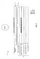
- FIG. 1illustrates a cross-section of an example electronic display projection assembly.
- FIG. 2illustrates a cross-section of an additional embodiment of the electronic display projection assembly.
- FIG. 3illustrates a prior art smartphone including an electronic display.
- FIGS. 4-5illustrate a smartphone implementing the electronic display projection assembly of FIG. 1 or FIG. 2 .
- FIG. 6illustrates a method of providing an image from an electronic display.
- FIG. 1illustrates a cross-section of an example electronic display projection assembly 10 that addresses the aforementioned problems of prior art electronic displays.
- the assembly 10includes an electronic display 12 , a transparent glass layer 14 , a projecting layer 16 , and a projection layer 17 .
- the electronic display 12comprises a liquid crystal display (LCD). LCDs are well known in the art, so operation of the LCD electronic display 12 will only be described briefly below.
- the LCD 12includes a liquid crystal display module 18 disposed between a pair of polarizing layers, namely a back polarizer 20 and a front polarizer 22 .
- the liquid crystal display module 18includes a liquid crystal layer 19 sandwiched between a thin-film transistor (TFT) array glass layer 24 and a color filter glass layer 30 .
- the liquid crystal layer 19may include twisted nematic (TN) liquid crystals or super-twisted nematic (STN) liquid crystals, for example.
- the TFT array glass layer 24is disposed between the liquid crystal layer 19 and the back polarizer 20 , and includes a plurality of transistors located in close proximity to the liquid crystal layer 19 .
- the LCD 12is OFF, the liquid crystals are oriented to block light from backlighting system 23 from passing through the polarizers 20 , 22 . In prior art devices, this causes LCDs to have a black appearance.
- the transistorscan be selectively actuated to apply a voltage to one or more of the liquid crystals, causing the crystals to rotate and permit light to pass through the polarizers 20 , 22 .
- An amount of voltage applied to a given liquid crystalcontrols the degree of rotation of that crystal, which in turn controls how much light passes through the polarizers 20 , 22 .
- Each of a plurality of pixels 26(a subset of them are shown in an enlarged view in FIG. 1 ) includes three individual sub-pixels 28 (e.g. red, green and blue sub-pixels - indicated by crosshatching in FIG. 1 ). By selectively controlling transistors behind each sub-pixel 28 , the sub-pixels 28 can be controlled to display colors via the color filter glass 30 .
- the TFT array glass layer 24controls the color of each pixel 26 of the electronic display 12 .
- the electronic display 12operates the TFT array glass 24 to controls a plurality of the pixels 26 to display images on the front polarizer 22 .
- the electronic display 12is illustrated as comprising an LCD, it is understood that an LCD is only one non-limiting example of an electronic display that could be used in the inventive projection assembly 10 .
- FIG. 1illustrates a cross-section of an example electronic display projection assembly 10 .
- the inventive assembly 10 of FIG. 1utilizes the projecting layer 16 to project the individual pixels 26 of the electronic display 12 through the glass layer 14 onto the projection layer 17 to display pixels 34 (which in turn include corresponding sub-pixels 36 ).
- the transparent glass layer 14is positioned on a side of the electronic display 12 on which the image is displayed (i.e., adjacent to an outermost surface of the front polarizer 22 ).
- the projecting layer 16is positioned between the electronic display 12 and the glass layer 14 . In FIG. 1 the projecting layer 16 and the projection layer 17 are located on opposite sides of the glass layer 14 .
- the projecting layer 16includes a plurality of microlenses for projecting the displayed image from the electronic display 12 through the glass layer 14 and onto the projection layer 17 .
- the projecting layer 16may be a plastic film including several plastic layers, such as those offered by Rolling Optics (http://www.rollingoptics.com/).
- the projection layer 17may be translucent, in that the layer 17 transmits some light, but is not completely transparent.
- the projection layer 17may be a film that is applied to the glass layer 14 .
- the projection layer 17may be treated to reflect substantially white light when the electronic display is in an OFF state, enabling the electronic display 12 to have a white, instead of a black, OFF state.
- whiteis only an example color, and the projection layer 17 could be treated to reflect another color when the electronic display 12 is in the OFF state.
- each pixel 26includes a plurality of sub-pixels 28 (in the example of FIG. 1 there are three sub-pixels 28 per pixel 26 ).
- each sub-pixel 28there is at least one corresponding transistor in the TFT array glass 24 layer.
- the microlensesmay be formed such that the area of each microlens is smaller than the area of each sub-pixel 28 . Additionally, the area of each microlens may be smaller than a spacing area between adjacent pixels 26 (i.e. an area of the space between the pixels 26 of FIG. 1 ) or an area between adjacent sub-pixels 28 .
- microlensesthat are sized as described above can help maintain image clarity by preventing blurring that may otherwise occur if individual microlenses overlapped adjacent pixels 26 or sub-pixels 28 .
- a large quantity of microlenseshas been described as being implemented in the layer 16 , in some embodiments, larger lenses or even a single large lens may be used in the layer 16 instead of the plurality of smaller microlenses.
- the layers 16 , 17are located on opposite sides of the transparent glass layer 14 .
- a zero (or substantially zero) distancemay be achieved from the surface of the glass 14 to the image on the projection layer 17 by projecting the displayed image closer to the viewing surface, which can mitigate the parallax effect described above.
- FIG. 2illustrates an alternate embodiment of the assembly (shown as 10 ′) in which the projecting layer 16 and the projection layer 17 are located on the same side of the glass layer (i.e., between the glass layer 14 and the electronic display 12 ).
- the projection layer 17is in closer proximity to, and perhaps even in contact with, the projecting layer 16 .
- some of the coatings described abovee.g. the hard coating, anti-fingerprint coating, etc.
- the thickness of the layers 14 , 16 , 17(shown as “A”) is on the order of 0.5 mm, and the thickness of the front polarizer 22 and color filter glass 30 (shown as “B”) is collectively also on the order of 0.5 mm.
- the thickness of the projection layer 16is on the order of 250 micrometers ( ⁇ m). Of course, these are only example values, and other thicknesses could be used.
- the projecting layer 16may be adjusted to facilitate image projection onto the outer edges contours of the glass layer 14 , such that active pixels can be displayed across the entire glass layer 14 , removing the need for a display border. This may be achieved by altering the angle of the microlenses in the layer 16 , such that the majority of the microlenses extend in a direction perpendicular to the surface 17 , but the outermost microlenses along opposite sides and possibly all four sides of the glass layer 14 (see, e.g., region 32 ) extend at an outward angle towards the sides of the projection layer 17 , to effectively bend the outer portion of the projected image. Although this may cause some minor image distortion at the outer portions of the layer 17 , active pixels could advantageously fill the entire area of the glass window 14 .
- the angled orientation of the microlensesis achieved by bending the layer 16 towards the backlight 23 and away from the layer 17 at those outermost edges (e.g., region 32 ).
- FIG. 3illustrates a prior art smartphone electronic device 40 that includes an electronic display (not shown) that projects onto a display area 42 , with the display area 42 having a black appearance (shown as crosshatching) when the device is in an OFF state.
- the display area 42does not extend all the way to the outer perimeter of the phone 42 , but instead is surrounded by a border 44 on the narrow sides.
- a display area 52 of the device 50reflects substantially white light to have a white appearance (see FIG. 4 ).
- an imageis projected on to the layer 17 of the display area 50 (see FIG. 5 ).
- the device 10is able to reduce the border 44 of the device 40 and to extend its image to the outermost sides of the device 50 , facilitating omission of the border 44 for example. Also, the device 10 is able to exhibit a substantially white off state, and to display its image closer to its viewing surface to provide an improved immersive user impression.
- FIG. 6schematically illustrates a corresponding method 100 of providing an image from the electronic display 12 of FIGS. 1-2 and is displayed on the electronic display 12 (step 102 ).
- the displayed imageis projected through the projecting layer 16 , which includes the plurality of microlenses, onto the projection layer 17 (step 104 ).
- the layers 16 , 17are located on opposite sides of the glass layer 14 , such that in step 104 the displayed image is projected through the plurality of microlenses and through the transparent glass layer 14 onto the projection layer 17 .
- the layers 16 , 17are on the same side of the glass layer 14 , such that the projection layer 17 is viewable through the glass layer 14 .
Landscapes
- Physics & Mathematics (AREA)
- Nonlinear Science (AREA)
- General Physics & Mathematics (AREA)
- Optics & Photonics (AREA)
- Crystallography & Structural Chemistry (AREA)
- Chemical & Material Sciences (AREA)
- Mathematical Physics (AREA)
- Engineering & Computer Science (AREA)
- Devices For Indicating Variable Information By Combining Individual Elements (AREA)
- Theoretical Computer Science (AREA)
- General Engineering & Computer Science (AREA)
- Human Computer Interaction (AREA)
- Liquid Crystal (AREA)
- Computer Hardware Design (AREA)
Abstract
Description
- The present invention generally relates to electronic displays, and more particularly relates to an electronic display projection assembly having a substantially white off state.
- Most existing electronic display technologies used in handheld devices exhibit a black off state, such that when these electronic displays are turned off they maintain a black appearance. This includes, for example, liquid crystal displays (LCDs), which are used in many electronic devices, such as smartphones, laptops, televisions, media players, computer monitors, and many other devices. The black off state has forced industrial designers to accommodate the color black into their products, and as a result a very large number of products with a black impression occupy the market.
- Another property exhibited by such displays is that a displayed image is generated at some depth below the surface of the device, with that image being viewed through a transparent glass surface. This can provide unwanted effects, such as a diminished immersive impression for users, and for touch screen devices can cause a parallax effect causing errors between the actual touch of finger and an intended touch area.
- Yet another issue with these prior art displays is that they require the presence of a border around a display area, because they are unable to extend the displayed image to the far outer periphery of their screens. So, for example, if a prior art smartphone has a glass display surface, the displayed image cannot fully extend to the outer boundary of that display surface, and must be surrounded by a border covering the non-display portions of the display surface.
- An electronic display projection assembly comprises an electronic display configured to display an image, and a transparent glass layer positioned on one side of the electronic display on which the image is displayed. A projection layer is located on a surface of the transparent glass layer. A projecting layer is positioned between the electronic display and the glass layer, and comprises a plurality of microlenses for projecting the displayed image onto the projection layer. The projecting and projection layers may be located on opposing sides of the transparent glass layer, or on the same side beneath the glass layer.
- A corresponding method of providing an image from an electronic display is also disclosed. According to the method, an image from an electronic display is displayed onto a projecting layer comprising a plurality of microlenses. The displayed image is projected through the plurality of microlenses and onto a projection layer on the transparent glass layer. The projecting and projection layers may be located on either opposite sides of the transparent glass layer, or on the same side beneath the glass layer.
- The projection layer may be translucent, may be treated to reflect substantially white light when the electronic display is in an OFF state, and may have an applied anti-reflective coating.
- The electronic display may be a liquid crystal display (LCD), and may include a collimated backlight. The transparent glass layer may comprise a touch screen input device.
- The projecting layer may be configured to stretch the projected image to the outer edges of the glass panel, and may be constructed of multiple plastic layers arranged to form the microlenses.
- In one or more embodiments, the electronic display has a plurality of pixels, with each pixel including at least three sub-pixels, and with an area of each microlens being smaller than an area of each sub-pixel.
- Of course, the present invention is not limited to the above features and advantages. Indeed, those skilled in the art will recognize additional features and advantages upon reading the following detailed description, and upon viewing the accompanying drawings.
FIG. 1 illustrates a cross-section of an example electronic display projection assembly.FIG. 2 illustrates a cross-section of an additional embodiment of the electronic display projection assembly.FIG. 3 illustrates a prior art smartphone including an electronic display.FIGS. 4-5 illustrate a smartphone implementing the electronic display projection assembly ofFIG. 1 orFIG. 2 .FIG. 6 illustrates a method of providing an image from an electronic display.FIG. 1 illustrates a cross-section of an example electronicdisplay projection assembly 10 that addresses the aforementioned problems of prior art electronic displays. Theassembly 10 includes anelectronic display 12, atransparent glass layer 14, aprojecting layer 16, and aprojection layer 17. In the example ofFIG. 1 , theelectronic display 12 comprises a liquid crystal display (LCD). LCDs are well known in the art, so operation of the LCDelectronic display 12 will only be described briefly below.- The
LCD 12 includes a liquidcrystal display module 18 disposed between a pair of polarizing layers, namely aback polarizer 20 and afront polarizer 22. The liquidcrystal display module 18 includes aliquid crystal layer 19 sandwiched between a thin-film transistor (TFT)array glass layer 24 and a colorfilter glass layer 30. Theliquid crystal layer 19 may include twisted nematic (TN) liquid crystals or super-twisted nematic (STN) liquid crystals, for example. The TFTarray glass layer 24 is disposed between theliquid crystal layer 19 and theback polarizer 20, and includes a plurality of transistors located in close proximity to theliquid crystal layer 19. When theLCD 12 is OFF, the liquid crystals are oriented to block light frombacklighting system 23 from passing through thepolarizers - However, the transistors can be selectively actuated to apply a voltage to one or more of the liquid crystals, causing the crystals to rotate and permit light to pass through the
polarizers polarizers FIG. 1 ) includes three individual sub-pixels28 (e.g. red, green and blue sub-pixels - indicated by crosshatching inFIG. 1 ). By selectively controlling transistors behind eachsub-pixel 28, thesub-pixels 28 can be controlled to display colors via thecolor filter glass 30. As such, the TFTarray glass layer 24 controls the color of eachpixel 26 of theelectronic display 12. Theelectronic display 12 operates theTFT array glass 24 to controls a plurality of thepixels 26 to display images on thefront polarizer 22. Of course, although theelectronic display 12 is illustrated as comprising an LCD, it is understood that an LCD is only one non-limiting example of an electronic display that could be used in theinventive projection assembly 10. FIG. 1 illustrates a cross-section of an example electronicdisplay projection assembly 10. Theinventive assembly 10 ofFIG. 1 utilizes theprojecting layer 16 to project theindividual pixels 26 of theelectronic display 12 through theglass layer 14 onto theprojection layer 17 to display pixels34 (which in turn include corresponding sub-pixels36). Thetransparent glass layer 14 is positioned on a side of theelectronic display 12 on which the image is displayed (i.e., adjacent to an outermost surface of the front polarizer22). The projectinglayer 16 is positioned between theelectronic display 12 and theglass layer 14. InFIG. 1 theprojecting layer 16 and theprojection layer 17 are located on opposite sides of theglass layer 14. Theprojecting layer 16 includes a plurality of microlenses for projecting the displayed image from theelectronic display 12 through theglass layer 14 and onto theprojection layer 17. The projectinglayer 16 may be a plastic film including several plastic layers, such as those offered by Rolling Optics (http://www.rollingoptics.com/).- In one or more embodiments, the
projection layer 17 may be translucent, in that thelayer 17 transmits some light, but is not completely transparent. Theprojection layer 17 may be a film that is applied to theglass layer 14. Theprojection layer 17 may be treated to reflect substantially white light when the electronic display is in an OFF state, enabling theelectronic display 12 to have a white, instead of a black, OFF state. Of course white is only an example color, and theprojection layer 17 could be treated to reflect another color when theelectronic display 12 is in the OFF state. - As discussed above, each
pixel 26 includes a plurality of sub-pixels28 (in the example ofFIG. 1 there are threesub-pixels 28 per pixel26). For eachsub-pixel 28, there is at least one corresponding transistor in theTFT array glass 24 layer. The microlenses may be formed such that the area of each microlens is smaller than the area of eachsub-pixel 28. Additionally, the area of each microlens may be smaller than a spacing area between adjacent pixels26 (i.e. an area of the space between thepixels 26 ofFIG. 1 ) or an area betweenadjacent sub-pixels 28. Utilizing microlenses that are sized as described above can help maintain image clarity by preventing blurring that may otherwise occur if individual microlenses overlappedadjacent pixels 26 orsub-pixels 28. Of course, although a large quantity of microlenses has been described as being implemented in thelayer 16, in some embodiments, larger lenses or even a single large lens may be used in thelayer 16 instead of the plurality of smaller microlenses. - In the embodiment of
FIG. 1 , thelayers transparent glass layer 14. With theprojection layer 17 being located on an exterior viewing surface of theassembly 10, a zero (or substantially zero) distance may be achieved from the surface of theglass 14 to the image on theprojection layer 17 by projecting the displayed image closer to the viewing surface, which can mitigate the parallax effect described above. In this embodiment, it may be desirable to apply an anti-reflective coating to the exterior of theprojection layer 17 to prevent undesirable reflections, and/or to include a hard coating or anti-fingerprint coating to prevent damage and fingerprints, respectively, from affecting theprojection layer 17. FIG. 2 illustrates an alternate embodiment of the assembly (shown as10′) in which the projectinglayer 16 and theprojection layer 17 are located on the same side of the glass layer (i.e., between theglass layer 14 and the electronic display12). In this embodiment, theprojection layer 17 is in closer proximity to, and perhaps even in contact with, the projectinglayer 16. In this embodiment, some of the coatings described above (e.g. the hard coating, anti-fingerprint coating, etc.) may be omitted, as theglass layer 14 shields thelayer 17 from user contact.- Referring again to
FIG. 1 , in one example the thickness of thelayers front polarizer 22 and color filter glass30 (shown as “B”) is collectively also on the order of 0.5 mm. By contrast, the thickness of theprojection layer 16 is on the order of 250 micrometers (μm). Of course, these are only example values, and other thicknesses could be used. - The projecting
layer 16 may be adjusted to facilitate image projection onto the outer edges contours of theglass layer 14, such that active pixels can be displayed across theentire glass layer 14, removing the need for a display border. This may be achieved by altering the angle of the microlenses in thelayer 16, such that the majority of the microlenses extend in a direction perpendicular to thesurface 17, but the outermost microlenses along opposite sides and possibly all four sides of the glass layer14 (see, e.g., region32) extend at an outward angle towards the sides of theprojection layer 17, to effectively bend the outer portion of the projected image. Although this may cause some minor image distortion at the outer portions of thelayer 17, active pixels could advantageously fill the entire area of theglass window 14. In one example, the angled orientation of the microlenses is achieved by bending thelayer 16 towards thebacklight 23 and away from thelayer 17 at those outermost edges (e.g., region32). FIG. 3 illustrates a prior art smartphoneelectronic device 40 that includes an electronic display (not shown) that projects onto adisplay area 42, with thedisplay area 42 having a black appearance (shown as crosshatching) when the device is in an OFF state. Notably, thedisplay area 42 does not extend all the way to the outer perimeter of thephone 42, but instead is surrounded by aborder 44 on the narrow sides.- Contrast this with the smartphone
electronic device 50 ofFIGS. 4-5 which implements the electronicdisplay projection assembly 10. As shown inFIG. 4 , when thedevice 50 is in an OFF state, adisplay area 52 of thedevice 50 reflects substantially white light to have a white appearance (seeFIG. 4 ). When thedevice 50 is in the ON state, an image is projected on to thelayer 17 of the display area50 (seeFIG. 5 ). - By implementing the teachings discussed above, the
device 10 is able to reduce theborder 44 of thedevice 40 and to extend its image to the outermost sides of thedevice 50, facilitating omission of theborder 44 for example. Also, thedevice 10 is able to exhibit a substantially white off state, and to display its image closer to its viewing surface to provide an improved immersive user impression. FIG. 6 schematically illustrates acorresponding method 100 of providing an image from theelectronic display 12 ofFIGS. 1-2 and is displayed on the electronic display12 (step102).- The displayed image is projected through the projecting
layer 16, which includes the plurality of microlenses, onto the projection layer17 (step104). - In one or more embodiments (see
FIG. 1 ), thelayers glass layer 14, such that instep 104 the displayed image is projected through the plurality of microlenses and through thetransparent glass layer 14 onto theprojection layer 17. Alternatively, in other embodiments (seeFIG. 2 ), thelayers glass layer 14, such that theprojection layer 17 is viewable through theglass layer 14. - Thus, the foregoing description and the accompanying drawings represent non-limiting examples of the methods and apparatus taught herein. As such, the present invention is not limited by the foregoing description and accompanying drawings. Instead, the present invention is limited only by the following claims and their legal equivalents.
Claims (21)
Priority Applications (1)
| Application Number | Priority Date | Filing Date | Title |
|---|---|---|---|
| US13/695,203US9063359B2 (en) | 2012-01-30 | 2012-02-28 | Electronic display projection assembly having substantially white off state |
Applications Claiming Priority (3)
| Application Number | Priority Date | Filing Date | Title |
|---|---|---|---|
| US201261592310P | 2012-01-30 | 2012-01-30 | |
| PCT/IB2012/050936WO2013114162A1 (en) | 2012-01-30 | 2012-02-28 | Electronic display projection assembly having substantially white off state |
| US13/695,203US9063359B2 (en) | 2012-01-30 | 2012-02-28 | Electronic display projection assembly having substantially white off state |
Publications (2)
| Publication Number | Publication Date |
|---|---|
| US20130258213A1true US20130258213A1 (en) | 2013-10-03 |
| US9063359B2 US9063359B2 (en) | 2015-06-23 |
Family
ID=45814535
Family Applications (1)
| Application Number | Title | Priority Date | Filing Date |
|---|---|---|---|
| US13/695,203Expired - Fee RelatedUS9063359B2 (en) | 2012-01-30 | 2012-02-28 | Electronic display projection assembly having substantially white off state |
Country Status (4)
| Country | Link |
|---|---|
| US (1) | US9063359B2 (en) |
| EP (1) | EP2641126B1 (en) |
| CN (1) | CN104094167B (en) |
| WO (1) | WO2013114162A1 (en) |
Cited By (6)
| Publication number | Priority date | Publication date | Assignee | Title |
|---|---|---|---|---|
| US20140092028A1 (en)* | 2012-09-28 | 2014-04-03 | Apple Inc. | Multiple-Element Light-Bending Structures for Minimizing Display Borders |
| US20170329182A1 (en)* | 2016-05-12 | 2017-11-16 | Google Inc. | Display assembly |
| US10436979B2 (en) | 2012-08-02 | 2019-10-08 | Apple Inc. | Displays with coherent fiber bundles |
| US20200026367A1 (en)* | 2018-07-20 | 2020-01-23 | Dell Products L.P. | System and Method of Utilizing Peripherals |
| US11258021B2 (en)* | 2018-10-11 | 2022-02-22 | Everdisplay Optronics (Shanghai) Co., Ltd | Display panel and display device having a step portion |
| US11488209B2 (en)* | 2019-06-18 | 2022-11-01 | Manicka Institute Llc | Apparatus, process, and system for display of images on windows of vehicles |
Families Citing this family (2)
| Publication number | Priority date | Publication date | Assignee | Title |
|---|---|---|---|---|
| CN105372869A (en)* | 2015-12-25 | 2016-03-02 | 武汉华星光电技术有限公司 | LCD (liquid crystal display) panel and LCD |
| US10347172B2 (en) | 2016-05-06 | 2019-07-09 | Vivint, Inc. | White or off-white hidden display apparatus, system, and method |
Citations (4)
| Publication number | Priority date | Publication date | Assignee | Title |
|---|---|---|---|---|
| US20030072080A1 (en)* | 2001-10-11 | 2003-04-17 | Nitto Denko Corporation | Optical sheet and display device having the optical sheet |
| US20110001712A1 (en)* | 2009-07-01 | 2011-01-06 | Toshiba Tec Kabushiki Kaisha | Display device |
| US20110246877A1 (en)* | 2010-04-05 | 2011-10-06 | Kwak Joonwon | Mobile terminal and image display controlling method thereof |
| US8144271B2 (en)* | 2006-08-03 | 2012-03-27 | Perceptive Pixel Inc. | Multi-touch sensing through frustrated total internal reflection |
Family Cites Families (5)
| Publication number | Priority date | Publication date | Assignee | Title |
|---|---|---|---|---|
| JPS57610A (en) | 1980-06-02 | 1982-01-05 | Hitachi Ltd | Liquid crystal display device |
| US6380994B1 (en) | 1995-07-28 | 2002-04-30 | Fujitsu Limited | Fresnel lens and liquid crystal display device |
| US6897911B2 (en)* | 2000-02-14 | 2005-05-24 | Fuji Photo Film Co., Ltd. | Light diffusing plate, liquid crystal display apparatus and rear projection apparatus |
| GB0322681D0 (en)* | 2003-09-27 | 2003-10-29 | Koninkl Philips Electronics Nv | Multi-view display |
| JP5122657B2 (en) | 2009-02-06 | 2013-01-16 | シャープ株式会社 | Display device |
- 2012
- 2012-02-28USUS13/695,203patent/US9063359B2/ennot_activeExpired - Fee Related
- 2012-02-28EPEP12708167.7Apatent/EP2641126B1/ennot_activeNot-in-force
- 2012-02-28WOPCT/IB2012/050936patent/WO2013114162A1/enactiveApplication Filing
- 2012-02-28CNCN201280068326.7Apatent/CN104094167B/ennot_activeExpired - Fee Related
Patent Citations (5)
| Publication number | Priority date | Publication date | Assignee | Title |
|---|---|---|---|---|
| US20030072080A1 (en)* | 2001-10-11 | 2003-04-17 | Nitto Denko Corporation | Optical sheet and display device having the optical sheet |
| US6822707B2 (en)* | 2001-10-11 | 2004-11-23 | Nitto Denko Corporation | Optical sheet and display device having the optical sheet |
| US8144271B2 (en)* | 2006-08-03 | 2012-03-27 | Perceptive Pixel Inc. | Multi-touch sensing through frustrated total internal reflection |
| US20110001712A1 (en)* | 2009-07-01 | 2011-01-06 | Toshiba Tec Kabushiki Kaisha | Display device |
| US20110246877A1 (en)* | 2010-04-05 | 2011-10-06 | Kwak Joonwon | Mobile terminal and image display controlling method thereof |
Cited By (16)
| Publication number | Priority date | Publication date | Assignee | Title |
|---|---|---|---|---|
| US10436979B2 (en) | 2012-08-02 | 2019-10-08 | Apple Inc. | Displays with coherent fiber bundles |
| US11860409B2 (en) | 2012-08-02 | 2024-01-02 | Apple Inc. | Displays with coherent fiber bundles |
| US11131803B2 (en) | 2012-08-02 | 2021-09-28 | Apple Inc. | Displays with coherent fiber bundles |
| US11573603B2 (en) | 2012-09-28 | 2023-02-07 | Apple Inc. | Multiple-element light-bending structures for minimizing display borders |
| US10067535B2 (en)* | 2012-09-28 | 2018-09-04 | Apple Inc. | Multiple-element light-bending structures for minimizing display borders |
| US20180292864A1 (en)* | 2012-09-28 | 2018-10-11 | Apple Inc. | Multiple-Element Light-Bending Structures For Minimizing Display Borders |
| US10551874B2 (en)* | 2012-09-28 | 2020-02-04 | Apple Inc. | Multiple-element light-bending structures for minimizing display borders |
| US20140092028A1 (en)* | 2012-09-28 | 2014-04-03 | Apple Inc. | Multiple-Element Light-Bending Structures for Minimizing Display Borders |
| US11112830B2 (en)* | 2012-09-28 | 2021-09-07 | Apple Inc. | Multiple-element light-bending structures for minimizing display borders |
| US20170329182A1 (en)* | 2016-05-12 | 2017-11-16 | Google Inc. | Display assembly |
| US10209563B2 (en)* | 2016-05-12 | 2019-02-19 | Google Llc | Non-black dead front display assembly |
| US10852859B2 (en)* | 2018-07-20 | 2020-12-01 | Dell Products L.P. | System and method of utilizing peripherals |
| US20200026367A1 (en)* | 2018-07-20 | 2020-01-23 | Dell Products L.P. | System and Method of Utilizing Peripherals |
| US11258021B2 (en)* | 2018-10-11 | 2022-02-22 | Everdisplay Optronics (Shanghai) Co., Ltd | Display panel and display device having a step portion |
| US11488209B2 (en)* | 2019-06-18 | 2022-11-01 | Manicka Institute Llc | Apparatus, process, and system for display of images on windows of vehicles |
| US11776015B2 (en) | 2019-06-18 | 2023-10-03 | Manicka Institute Llc | Apparatus, process, and system for display of images on windows of vehicles |
Also Published As
| Publication number | Publication date |
|---|---|
| CN104094167B (en) | 2017-06-06 |
| US9063359B2 (en) | 2015-06-23 |
| CN104094167A (en) | 2014-10-08 |
| EP2641126B1 (en) | 2017-03-22 |
| EP2641126A1 (en) | 2013-09-25 |
| WO2013114162A1 (en) | 2013-08-08 |
Similar Documents
| Publication | Publication Date | Title |
|---|---|---|
| US9063359B2 (en) | Electronic display projection assembly having substantially white off state | |
| US10859869B2 (en) | Display device | |
| CN104575322B (en) | A kind of two-d display panel and display device | |
| CN102483530B (en) | Display panel, display system, portable terminal and electronic device | |
| US20180299726A1 (en) | Display device | |
| US9472148B2 (en) | Liquid crystal display device having gate sharing structure and method of driving the same | |
| US9651818B2 (en) | Liquid crystal display panel comprising different spacing distances between pixel electrodes corresponding to specific color resist blocks | |
| US10268069B2 (en) | Transparent liquid crystal display | |
| JP5628611B2 (en) | Liquid crystal display | |
| KR102135935B1 (en) | Display Device With Narrow Bezel | |
| CN101799599A (en) | Stereoscopic display and display method thereof | |
| US20150253608A1 (en) | Liquid crystal display device | |
| US10197843B2 (en) | Array substrate, color film substrate, and display device | |
| CN104020599A (en) | Display system | |
| US20140347614A1 (en) | Liquid crystal display device | |
| CN111679461A (en) | Display device with switchable field of view and display method thereof | |
| EP3690538B1 (en) | Display panel, display device, and driving method thereof | |
| KR100873025B1 (en) | Fringe-field switching liquid crystal display with adjustable viewing angle | |
| CN108333838A (en) | Display base plate, display panel and display device | |
| US20150049068A1 (en) | Liquid crystal display panel and 3d image system | |
| KR101738002B1 (en) | Liquid crystal display | |
| JP7398926B2 (en) | liquid crystal display device | |
| KR101948827B1 (en) | Transparent Liquid Crystal Display Device | |
| TWI391715B (en) | Color filter substrate and liquid crystal display | |
| CN106908984B (en) | A kind of display panel, its display methods and display device |
Legal Events
| Date | Code | Title | Description |
|---|---|---|---|
| AS | Assignment | Owner name:SONY MOBILE COMMUNICATIONS AB, SWEDEN Free format text:ASSIGNMENT OF ASSIGNORS INTEREST;ASSIGNOR:EK, MARTIN;REEL/FRAME:029583/0862 Effective date:20121220 | |
| AS | Assignment | Owner name:SONY MOBILE COMMUNICATIONS AB, SWEDEN Free format text:ASSIGNMENT OF ASSIGNORS INTEREST;ASSIGNOR:SONY MOBILE COMMUNICATIONS AB;REEL/FRAME:035604/0936 Effective date:20150408 Owner name:SONY CORPORATION, JAPAN Free format text:ASSIGNMENT OF ASSIGNORS INTEREST;ASSIGNOR:SONY MOBILE COMMUNICATIONS AB;REEL/FRAME:035604/0936 Effective date:20150408 | |
| STCF | Information on status: patent grant | Free format text:PATENTED CASE | |
| AS | Assignment | Owner name:SONY MOBILE COMMUNICATIONS INC., JAPAN Free format text:ASSIGNMENT OF ASSIGNORS INTEREST;ASSIGNOR:SONY CORPORATION;REEL/FRAME:043943/0631 Effective date:20170914 | |
| AS | Assignment | Owner name:SONY MOBILE COMMUNICATIONS INC., JAPAN Free format text:ASSIGNMENT OF ASSIGNORS INTEREST;ASSIGNOR:SONY MOBILE COMMUNICATIONS AB;REEL/FRAME:043951/0529 Effective date:20170912 | |
| FEPP | Fee payment procedure | Free format text:MAINTENANCE FEE REMINDER MAILED (ORIGINAL EVENT CODE: REM.); ENTITY STATUS OF PATENT OWNER: LARGE ENTITY | |
| LAPS | Lapse for failure to pay maintenance fees | Free format text:PATENT EXPIRED FOR FAILURE TO PAY MAINTENANCE FEES (ORIGINAL EVENT CODE: EXP.); ENTITY STATUS OF PATENT OWNER: LARGE ENTITY | |
| STCH | Information on status: patent discontinuation | Free format text:PATENT EXPIRED DUE TO NONPAYMENT OF MAINTENANCE FEES UNDER 37 CFR 1.362 | |
| FP | Lapsed due to failure to pay maintenance fee | Effective date:20190623 |