US20130256827A1 - Efficient pitch multiplication process - Google Patents
Efficient pitch multiplication processDownload PDFInfo
- Publication number
- US20130256827A1 US20130256827A1US13/902,675US201313902675AUS2013256827A1US 20130256827 A1US20130256827 A1US 20130256827A1US 201313902675 AUS201313902675 AUS 201313902675AUS 2013256827 A1US2013256827 A1US 2013256827A1
- Authority
- US
- United States
- Prior art keywords
- integrated circuit
- spacers
- layer
- hard mask
- mask
- Prior art date
- Legal status (The legal status is an assumption and is not a legal conclusion. Google has not performed a legal analysis and makes no representation as to the accuracy of the status listed.)
- Granted
Links
- 238000000034methodMethods0.000titledescription63
- 230000008569processEffects0.000titledescription22
- 125000006850spacer groupChemical group0.000claimsabstractdescription117
- 239000000463materialSubstances0.000claimsabstractdescription76
- 239000000758substrateSubstances0.000claimsabstractdescription53
- 229920002120photoresistant polymerPolymers0.000claimsabstractdescription47
- 229910003481amorphous carbonInorganic materials0.000claimsabstractdescription14
- 239000010410layerSubstances0.000claimsdescription172
- 230000015654memoryEffects0.000claimsdescription23
- 239000011241protective layerSubstances0.000claimsdescription16
- 229910052710siliconInorganic materials0.000claimsdescription9
- 239000010703siliconSubstances0.000claimsdescription9
- 229910052814silicon oxideInorganic materials0.000claimsdescription9
- VYPSYNLAJGMNEJ-UHFFFAOYSA-NSilicium dioxideChemical compoundO=[Si]=OVYPSYNLAJGMNEJ-UHFFFAOYSA-N0.000claimsdescription7
- XUIMIQQOPSSXEZ-UHFFFAOYSA-NSiliconChemical compound[Si]XUIMIQQOPSSXEZ-UHFFFAOYSA-N0.000claimsdescription7
- OKTJSMMVPCPJKN-UHFFFAOYSA-NCarbonChemical compound[C]OKTJSMMVPCPJKN-UHFFFAOYSA-N0.000claimsdescription5
- 229910052799carbonInorganic materials0.000claimsdescription5
- 229910052581Si3N4Inorganic materials0.000claimsdescription4
- HQVNEWCFYHHQES-UHFFFAOYSA-Nsilicon nitrideChemical compoundN12[Si]34N5[Si]62N3[Si]51N64HQVNEWCFYHHQES-UHFFFAOYSA-N0.000claimsdescription4
- 239000006117anti-reflective coatingSubstances0.000claimsdescription3
- 239000011368organic materialSubstances0.000claims2
- 238000000926separation methodMethods0.000claims2
- 238000012545processingMethods0.000abstractdescription10
- 230000001681protective effectEffects0.000abstractdescription7
- 239000011295pitchSubstances0.000description86
- 238000000206photolithographyMethods0.000description12
- 238000005530etchingMethods0.000description9
- 238000003491arrayMethods0.000description8
- 238000000151depositionMethods0.000description8
- 238000004519manufacturing processMethods0.000description7
- 238000000059patterningMethods0.000description7
- 238000012546transferMethods0.000description7
- 230000015572biosynthetic processEffects0.000description6
- 239000012212insulatorSubstances0.000description6
- 238000005229chemical vapour depositionMethods0.000description5
- -1i.e.Polymers0.000description5
- 230000000873masking effectEffects0.000description5
- 230000002093peripheral effectEffects0.000description5
- 230000002829reductive effectEffects0.000description5
- 239000003990capacitorSubstances0.000description4
- 230000003247decreasing effectEffects0.000description4
- 230000008021depositionEffects0.000description4
- 239000000203mixtureSubstances0.000description4
- 239000004020conductorSubstances0.000description3
- NBVXSUQYWXRMNV-UHFFFAOYSA-NfluoromethaneChemical compoundFCNBVXSUQYWXRMNV-UHFFFAOYSA-N0.000description3
- 238000012986modificationMethods0.000description3
- 230000004048modificationEffects0.000description3
- 230000005855radiationEffects0.000description3
- 238000003860storageMethods0.000description3
- 102100022717Atypical chemokine receptor 1Human genes0.000description2
- KAKZBPTYRLMSJV-UHFFFAOYSA-NButadieneChemical compoundC=CC=CKAKZBPTYRLMSJV-UHFFFAOYSA-N0.000description2
- XPDWGBQVDMORPB-UHFFFAOYSA-NFluoroformChemical compoundFC(F)FXPDWGBQVDMORPB-UHFFFAOYSA-N0.000description2
- 101000678879Homo sapiens Atypical chemokine receptor 1Proteins0.000description2
- ATUOYWHBWRKTHZ-UHFFFAOYSA-NPropaneChemical compoundCCCATUOYWHBWRKTHZ-UHFFFAOYSA-N0.000description2
- 238000004380ashingMethods0.000description2
- QVGXLLKOCUKJST-UHFFFAOYSA-Natomic oxygenChemical compound[O]QVGXLLKOCUKJST-UHFFFAOYSA-N0.000description2
- 238000005520cutting processMethods0.000description2
- RWRIWBAIICGTTQ-UHFFFAOYSA-NdifluoromethaneChemical compoundFCFRWRIWBAIICGTTQ-UHFFFAOYSA-N0.000description2
- 238000011065in-situ storageMethods0.000description2
- 238000001127nanoimprint lithographyMethods0.000description2
- 239000001301oxygenSubstances0.000description2
- 229910052760oxygenInorganic materials0.000description2
- 230000009467reductionEffects0.000description2
- 239000004065semiconductorSubstances0.000description2
- 238000005549size reductionMethods0.000description2
- 239000000126substanceSubstances0.000description2
- 239000011800void materialSubstances0.000description2
- RYGMFSIKBFXOCR-UHFFFAOYSA-NCopperChemical compound[Cu]RYGMFSIKBFXOCR-UHFFFAOYSA-N0.000description1
- VZPPHXVFMVZRTE-UHFFFAOYSA-N[Kr]FChemical compound[Kr]FVZPPHXVFMVZRTE-UHFFFAOYSA-N0.000description1
- 238000007792additionMethods0.000description1
- 229910052782aluminiumInorganic materials0.000description1
- XAGFODPZIPBFFR-UHFFFAOYSA-NaluminiumChemical compound[Al]XAGFODPZIPBFFR-UHFFFAOYSA-N0.000description1
- 229910021417amorphous siliconInorganic materials0.000description1
- ISQINHMJILFLAQ-UHFFFAOYSA-Nargon hydrofluorideChemical compoundF.[Ar]ISQINHMJILFLAQ-UHFFFAOYSA-N0.000description1
- 238000000231atomic layer depositionMethods0.000description1
- 230000004888barrier functionEffects0.000description1
- 230000009286beneficial effectEffects0.000description1
- 239000001273butaneSubstances0.000description1
- 239000007833carbon precursorSubstances0.000description1
- 238000000576coating methodMethods0.000description1
- 150000001875compoundsChemical class0.000description1
- 238000007596consolidation processMethods0.000description1
- 239000000470constituentSubstances0.000description1
- 229910052802copperInorganic materials0.000description1
- 239000010949copperSubstances0.000description1
- 230000007547defectEffects0.000description1
- 238000009792diffusion processMethods0.000description1
- 230000003292diminished effectEffects0.000description1
- 238000010894electron beam technologyMethods0.000description1
- 230000005669field effectEffects0.000description1
- 230000006870functionEffects0.000description1
- 150000002430hydrocarbonsChemical class0.000description1
- 238000007654immersionMethods0.000description1
- 229910010272inorganic materialInorganic materials0.000description1
- 239000011147inorganic materialSubstances0.000description1
- 239000011810insulating materialSubstances0.000description1
- 238000005468ion implantationMethods0.000description1
- 238000002955isolationMethods0.000description1
- 238000001459lithographyMethods0.000description1
- 229910052751metalInorganic materials0.000description1
- 239000002184metalSubstances0.000description1
- 238000001465metallisationMethods0.000description1
- IJDNQMDRQITEOD-UHFFFAOYSA-Nn-butaneChemical compoundCCCCIJDNQMDRQITEOD-UHFFFAOYSA-N0.000description1
- OFBQJSOFQDEBGM-UHFFFAOYSA-Nn-pentaneNatural productsCCCCCOFBQJSOFQDEBGM-UHFFFAOYSA-N0.000description1
- 150000004767nitridesChemical class0.000description1
- 230000001590oxidative effectEffects0.000description1
- 238000005498polishingMethods0.000description1
- 229910021420polycrystalline siliconInorganic materials0.000description1
- 229920000642polymerPolymers0.000description1
- 229920005591polysiliconPolymers0.000description1
- 239000002243precursorSubstances0.000description1
- 239000001294propaneSubstances0.000description1
- QQONPFPTGQHPMA-UHFFFAOYSA-NpropyleneNatural productsCC=CQQONPFPTGQHPMA-UHFFFAOYSA-N0.000description1
- 125000004805propylene groupChemical group[H]C([H])([H])C([H])([*:1])C([H])([H])[*:2]0.000description1
- MWWATHDPGQKSAR-UHFFFAOYSA-NpropyneChemical compoundCC#CMWWATHDPGQKSAR-UHFFFAOYSA-N0.000description1
- 230000007261regionalizationEffects0.000description1
- 230000000717retained effectEffects0.000description1
- 229910021332silicideInorganic materials0.000description1
- FVBUAEGBCNSCDD-UHFFFAOYSA-Nsilicide(4-)Chemical compound[Si-4]FVBUAEGBCNSCDD-UHFFFAOYSA-N0.000description1
- LIVNPJMFVYWSIS-UHFFFAOYSA-Nsilicon monoxideChemical class[Si-]#[O+]LIVNPJMFVYWSIS-UHFFFAOYSA-N0.000description1
- 239000002356single layerSubstances0.000description1
- 239000007787solidSubstances0.000description1
- 230000003068static effectEffects0.000description1
- 125000000383tetramethylene groupChemical group[H]C([H])([*:1])C([H])([H])C([H])([H])C([H])([H])[*:2]0.000description1
- 230000007704transitionEffects0.000description1
- WFKWXMTUELFFGS-UHFFFAOYSA-NtungstenChemical compound[W]WFKWXMTUELFFGS-UHFFFAOYSA-N0.000description1
- 229910052721tungstenInorganic materials0.000description1
- 239000010937tungstenSubstances0.000description1
- 238000005019vapor deposition processMethods0.000description1
Images


Classifications
- H01L29/06—
- H—ELECTRICITY
- H01—ELECTRIC ELEMENTS
- H01L—SEMICONDUCTOR DEVICES NOT COVERED BY CLASS H10
- H01L21/00—Processes or apparatus adapted for the manufacture or treatment of semiconductor or solid state devices or of parts thereof
- H01L21/02—Manufacture or treatment of semiconductor devices or of parts thereof
- H01L21/027—Making masks on semiconductor bodies for further photolithographic processing not provided for in group H01L21/18 or H01L21/34
- H01L21/033—Making masks on semiconductor bodies for further photolithographic processing not provided for in group H01L21/18 or H01L21/34 comprising inorganic layers
- H01L21/0334—Making masks on semiconductor bodies for further photolithographic processing not provided for in group H01L21/18 or H01L21/34 comprising inorganic layers characterised by their size, orientation, disposition, behaviour, shape, in horizontal or vertical plane
- H01L21/0338—Process specially adapted to improve the resolution of the mask
- H—ELECTRICITY
- H01—ELECTRIC ELEMENTS
- H01L—SEMICONDUCTOR DEVICES NOT COVERED BY CLASS H10
- H01L21/00—Processes or apparatus adapted for the manufacture or treatment of semiconductor or solid state devices or of parts thereof
- H01L21/02—Manufacture or treatment of semiconductor devices or of parts thereof
- H01L21/04—Manufacture or treatment of semiconductor devices or of parts thereof the devices having potential barriers, e.g. a PN junction, depletion layer or carrier concentration layer
- H01L21/18—Manufacture or treatment of semiconductor devices or of parts thereof the devices having potential barriers, e.g. a PN junction, depletion layer or carrier concentration layer the devices having semiconductor bodies comprising elements of Group IV of the Periodic Table or AIIIBV compounds with or without impurities, e.g. doping materials
- H01L21/30—Treatment of semiconductor bodies using processes or apparatus not provided for in groups H01L21/20 - H01L21/26
- H01L21/302—Treatment of semiconductor bodies using processes or apparatus not provided for in groups H01L21/20 - H01L21/26 to change their surface-physical characteristics or shape, e.g. etching, polishing, cutting
- H01L21/306—Chemical or electrical treatment, e.g. electrolytic etching
- H01L21/308—Chemical or electrical treatment, e.g. electrolytic etching using masks
- H01L21/3083—Chemical or electrical treatment, e.g. electrolytic etching using masks characterised by their size, orientation, disposition, behaviour, shape, in horizontal or vertical plane
- H01L21/3088—Process specially adapted to improve the resolution of the mask
- H—ELECTRICITY
- H10—SEMICONDUCTOR DEVICES; ELECTRIC SOLID-STATE DEVICES NOT OTHERWISE PROVIDED FOR
- H10D—INORGANIC ELECTRIC SEMICONDUCTOR DEVICES
- H10D62/00—Semiconductor bodies, or regions thereof, of devices having potential barriers
- H10D62/10—Shapes, relative sizes or dispositions of the regions of the semiconductor bodies; Shapes of the semiconductor bodies
- H—ELECTRICITY
- H10—SEMICONDUCTOR DEVICES; ELECTRIC SOLID-STATE DEVICES NOT OTHERWISE PROVIDED FOR
- H10D—INORGANIC ELECTRIC SEMICONDUCTOR DEVICES
- H10D89/00—Aspects of integrated devices not covered by groups H10D84/00 - H10D88/00
Definitions
- This inventionrelates generally to integrated circuit fabrication and, more particularly, to masking techniques.
- integrated circuitsare continuously being reduced in size.
- the sizes of the constituent features that form the integrated circuitse.g., electrical devices and interconnect lines, are also constantly being decreased to facilitate this size reduction.
- DRAMdynamic random access memories
- SRAMstatic random access memories
- FEferroelectric
- a DRAM memory celltypically consists of two electrical devices: a storage capacitor and an access field effect transistor. Each memory cell is an addressable location that can store one bit (binary digit) of data. A bit can be written to a cell through the transistor and can be read by sensing charge in the capacitor.
- the memory devicescan be made smaller. Additionally, storage capacities can be increased by fitting more memory cells on a given area in the memory devices.
- Other memory designscan integrate access and storage devices or omit access devices (e.g., cross-point MRAM, PCRAM, etc.).
- Pitchis defined as the distance between an identical point in two neighboring features of a repeating pattern. These features are typically defined by spaces between adjacent features, which spaces are typically filled by a material, such as an insulator. As a result, pitch can be viewed as the sum of the width of a feature and of the width of the space on one side of the feature separating that feature from a neighboring feature.
- photolithography techniqueseach have a minimum pitch below which a particular photolithographic technique cannot reliably form features. Thus, the minimum pitch of a photolithographic technique is an obstacle to continued feature size reduction.
- Pitch doubling” or “pitch multiplication”is one proposed method for extending the capabilities of photolithographic techniques beyond their minimum pitch.
- a pitch multiplication methodis illustrated in FIGS. 1A-1F and described in U.S. Pat. No. 5,328,810, issued to Lowrey et al., the entire disclosure of which is incorporated herein by reference.
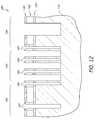
- a pattern of lines 10is photolithographically formed in a photoresist layer, which overlies a layer 20 of an expendable material, which in turn overlies a substrate 30 . As shown in FIG.
- the patternis then transferred using an etch (preferably an anisotropic etch) to the layer 20 , thereby forming placeholders, or mandrels, 40 .
- the photoresist lines 10can be stripped and the mandrels 40 can be isotropically etched to increase the distance between neighboring mandrels 40 , as shown in FIG. 1C .
- a layer 50 of spacer materialis subsequently deposited over the mandrels 40 , as shown in FIG. 1D .
- Spacers 60( FIG. 1E ), i.e., the material extending or originally formed extending from sidewalls of another material, are then formed on the sides of the mandrels 40 .
- the spacer formationis accomplished by preferentially etching the spacer material from the horizontal surfaces 70 and 80 in a directional spacer etch, as shown in FIG. 1E .
- the remaining mandrels 40are then removed, leaving behind only the spacers 60 , which together act as a mask for patterning, as shown in FIG. 1F .
- the same widthnow includes two mask elements and two spaces, with the spaces defined by, e.g., the spacers 60 .
- the smallest feature size that can be formed with a photolithographic techniqueis effectively decreased.
- pitch doublingthis reduction in pitch is conventionally referred to as pitch “doubling,” or, more generally, pitch “multiplication.”
- pitch “multiplication” of pitch by a certain factoractually involves reducing the pitch by that factor.
- the conventional terminologyis retained herein.
- the layer 50 of spacer materialtypically has a single thickness 90 (see FIGS. 1D and 1E ) and because the sizes of the mask elements formed by the spacers 60 usually correspond to that thickness 90 , pitch doubling typically produces mask elements of only one width.
- Circuitsgenerally employ features of different sizes.
- random access memory circuitstypically contain arrays of memory cells located in one part of the circuits and logic circuits located in the so-called “periphery.” In the arrays, the memory cells are typically connected by conductive lines and, in the periphery, the conductive lines typically contact interconnects in the periphery or landing pads for connecting arrays to logic. Peripheral features such as peripheral interconnects and landing pads, however, can be larger than the conductive lines in the array.
- peripheral transistorscan be larger than the electrical devices in the array.
- electrical devices in the peripheryincluding peripheral transistors, can be larger than the electrical devices in the array.
- peripheral featurescan be formed with the same pitch as features in the array, because mask patterns formed by pitch multiplication may be limited to those that are formed along the sidewalls of patterned photoresist, it is challenging to employ pitch multiplication while achieving the flexibility, e.g., geometric flexibility, required to define some features.
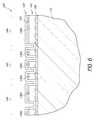
- FIGS. 1A-1Fare schematic, cross-sectional side views of a sequence of masking patterns for forming conductive lines, in accordance with a prior art pitch doubling method
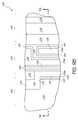
- FIG. 2Ais a schematic top plan view of a partially formed integrated circuit, in accordance with preferred embodiments of the invention.
- FIG. 2Bis a schematic cross-sectional side view of the partially formed integrated circuit of FIG. 2A , in accordance with preferred embodiments of the invention.
- FIG. 3is a schematic cross-sectional side view of the partially formed integrated circuit of FIGS. 2A-2B after forming lines in a photoresist layer, in accordance with preferred embodiments of the invention
- FIG. 4is a schematic cross-sectional side view of the partially formed integrated circuit of FIG. 3 after transferring the pattern in the photoresist layer to underlying hard mask and temporary layers and removing the photoresist layer, in accordance with preferred embodiments of the invention;
- FIG. 5is a schematic, cross-sectional side view of the partially formed integrated circuit of FIG. 4 after performing a trim etch to widen spaces between mask elements, in accordance with preferred embodiments of the invention
- FIG. 6is a schematic, cross-sectional side view of the partially formed integrated circuit of FIG. 5 after depositing a layer of a spacer material, in accordance with preferred embodiments of the invention
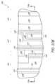
- FIGS. 7A-7Bare schematic, cross-sectional side and top plan views of the partially formed integrated circuit of FIG. 6 after performing a spacer etch, in accordance with preferred embodiments of the invention.
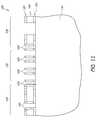
- FIG. 8is a schematic, cross-sectional side view of the partially formed integrated circuit of FIGS. 7A-7B after depositing a layer of protective material, in accordance with preferred embodiments of the invention.
- FIGS. 9A-9Bare schematic, cross-sectional side and top plan views of the partially formed integrated circuit of FIG. 8 after patterning the protective layer to expose mask elements in the array region and other selected areas of the partially formed integrated circuit, in accordance with preferred embodiments of the invention.
- FIGS. 10A-10Bare schematic, cross-sectional side and top plan views of the partially formed integrated circuit of FIGS. 9A-9B after removing hard mask and temporary layer material in regions exposed by the patterned protective layer, thereby leaving a pattern of free-standing spacers, and subsequent removal of the protective layer, in accordance with preferred embodiments of the invention;
- FIG. 11is a schematic, cross-sectional side view of the partially formed integrated circuit of FIGS. 10A-10B after etching the pattern of pitch multiplied and non-pitch multiplied mask elements into an underlying hard mask layer, in accordance with preferred embodiments of the invention;
- FIG. 12is a schematic, cross-sectional side view of the partially formed integrated circuit of FIG. 11 after transferring the pattern of pitch multiplied and non-pitch multiplied mask elements to the underlying substrate, in accordance with preferred embodiments of the invention;
- FIG. 13is a schematic, cross-sectional side view of the partially formed integrated circuit of FIG. 12 after removing mask elements overlying the substrate, in accordance with other preferred embodiments of the invention.
- FIG. 14is a schematic, cross-sectional side view of the partially formed integrated circuit of FIG. 12 or 13 after removing all mask elements overlying the substrate, in accordance with other preferred embodiments of the invention.
- pitch multiplied featuresare typically too small and/or closely spaced to reliably contact features such as contact plugs or larger sized interconnects. Shorting or other misalignments can occur because of the small size and/or close spacing of the pitch multiplied features.
- Various strategieshave been proposed for forming pitch multiplied and non-pitch multiplied features. Exemplary methods for forming pitch multiplied and non-pitch multiplied features are described in U.S. patent application Ser. No. 10/934,778 to Abatchev et al. and U.S. patent application Ser. No. 10/931,771 to Tran et al., both of which are assigned to the assignee of the present application. The entire disclosures of each of these references are incorporated by reference herein.
- the process flowscan be complicated, due to the need to form and overlay features of different sizes.
- the pitch multiplied featurescan be formed separately from the larger sized features, thereby requiring multiple mask formation and mask consolidation steps.
- each additional step in a process flowcan undesirably add to the complexity and expense of a process flow.
- each additional stephas the possibility of introducing misalignments and etch and pattern transfer complications and other errors which can cause undesirable variations in process results.
- preferred embodiments of the inventionallow for the formation and connection of pitch multiplied and non-pitch multiplied features using an advantageously simple process flow.
- parts of a selectively definable layere.g., a photoresist layer
- Pitch multiplicationis used to form pitch multiplied spacers in the array region.
- At least some parts of the interface and the periphery regionsare protected using a protective material while other parts are etched and free-standing spacers are formed in the array region.
- the protective materialis then removed and a pattern including spacers in the array region and features in the interface and the periphery regions are then transferred to a hard mask layer.
- the hard mask layercan be used to pattern an underlying substrate.
- processing according to the preferred embodimentsallows for the formation and connection of pitch-multiplied to non-pitch multiplied features using relatively few process steps.
- the relatively small number of stepscan improve the uniformity of process results. Non-uniformities introduced by additional pattern formation and pattern transfer steps can be reduced.
- connections of non-pitch multiplied mask elements to pitch multiplied mask elementscan be formed simultaneously on the same vertical level with the non-pitch multiplied mask elements, defects caused by misaligning separately formed mask elements can be reduced.
- connections to pitch multiplied featurescan be formed more reliably, thereby reducing the possibility of shorts and poorly connected pitch-multiplied features.
- the relatively low number of process stepsadvantageously allows for the fabrication of integrated circuits with high throughput and relatively low cost.
- a stack of layers suitable for forming a pattern in a hard mask layeris formed.
- a top view of a partially fabricated integrated circuit 100is shown. While the preferred embodiments can be used to form any integrated circuit, they are particularly advantageously applied to form devices having arrays of electrical devices, including memory cell arrays for volatile and non-volatile memory devices such as DRAM, ROM or flash memory, including NAND flash memory, or integrated circuits having logic or gate arrays.
- the logic arraycan be a field programmable gate array (FPGA) having a core array similar to a memory array and a periphery with supporting logics.
- the integrated circuit 100can be, e.g., a memory chip or a processor, which can include both a logic array and embedded memory, or any other integrated circuit having arrays of features, such as a logic or a gate array.
- a central region 102the array region or simply “array,” is surrounded by a interface region 104 , which is surrounded by a peripheral region 106 , also referred to as the “periphery.”
- the array 102will typically be densely populated with conducting lines and electrical devices such as transistors and capacitors.
- the electrical devicesform a plurality of memory cells, which are typically arranged in a regular grid pattern at the intersection of word lines and bit lines.
- pitch multiplicationcan be used to form features such as rows and/or columns of transistors and capacitors in the array 102 , as discussed below.
- the periphery 106typically comprises features larger than those in the array 102 .
- Conventional photolithography, rather than pitch multiplication,is preferably used to pattern features, such as logic circuitry, in the periphery 106 , because the geometric complexity of logic circuits located in the periphery 106 makes using pitch multiplication difficult.
- features in the periphery 106typically do not have the repeating regularity of features typical in the array 102 .
- the logic areaneed not be as dense as the array regions 102 , such that pitch multiplication in the logic area is unnecessary.
- the regular grid typical of array patternsis conducive to pitch multiplication.
- some devices in the peripheryrequire larger geometries due to electrical constraints, thereby making pitch multiplication less advantageous than conventional photolithography for such devices.
- the interface region 104can contain both array and periphery features.
- the interface region 104can serve as a transition from the array 102 to the periphery 106 and allow contact between features in the array 102 and features in the periphery 106 .
- the relative positions, and the number of array 102 , interface 104 and periphery 106 regions in the integrated circuit 100may vary from that depicted.
- the interface 104 and periphery 106 regionsmay be disposed directly with either side of the array region 102 , as illustrated in some of the figures below.
- certain specific characteristics of these regionshave been noted above and clear demarcations between the regions have been illustrated for ease of discussion, in some arrangements, two or more of the regions can overlap.
- FIG. 2Bshows a cross-sectional side view of the partially formed integrated circuit 100 .
- Various masking layers 120 - 150are preferably provided above a substrate 110 .
- the layers 120 - 150will be etched to form a mask for patterning the substrate 110 , as discussed below.
- the materials for the layers 120 - 150 overlying the substrate 110are preferably chosen based upon consideration of the chemistry and process conditions for the various pattern forming and pattern transferring steps discussed herein. Because the layers between a topmost selectively definable (e.g., photodefinable) layer 120 and the substrate 110 preferably function to transfer a pattern derived from the selectively definable layer 120 to the substrate 110 , the layers 130 - 150 between the selectively definable layer 120 and the substrate 110 are preferably chosen so that they can be selectively etched relative to other exposed materials.
- a topmost selectively definable layer 120 and the substrate 110preferably function to transfer a pattern derived from the selectively definable layer 120 to the substrate 110
- the layers 130 - 150 between the selectively definable layer 120 and the substrate 110are preferably chosen so that they can be selectively etched relative to other exposed materials.
- a materialis considered selectively, or preferentially, etched when the etch rate for that material is at least about 2-3 times greater, preferably at least about 10 times greater, more preferably at least about 20 times greater and, most preferably, at least about 50 times greater than that for surrounding materials. Because a goal of the layers 120 - 140 overlying a second hard mask layer 150 is to allow well-defined patterns to be formed in the second hard mask layer 150 , it will be appreciated that one or more of the layers 120 - 140 can be omitted or substituted if suitable other materials, chemistries and/or process conditions are used.
- the selectively definable layer 120overlies a first hard mask, or etch stop, layer 130 , which overlies a temporary layer 140 , which overlies the second hard mask, or etch stop, layer 150 , which overlies the substrate 110 to be processed (e.g., etched) through a mask.
- the mask through which the substrate 110 is processedis formed in the second hard mask layer 150 .
- the selectively definable layer 120is preferably photodefinable, e.g., formed of a photoresist, including any photoresist known in the art.
- the photoresistcan be any photoresist compatible with 157 nm, 193 nm, 248 nm or 365 nm wavelength systems, 193 nm wavelength immersion systems, extreme ultraviolet systems (including 13.7 nm wavelength systems) or electron beam lithographic systems.
- maskless lithography, or maskless photolithographycan be used to define the photodefinable layer 120 .
- photoresist materialsinclude argon fluoride (ArF) sensitive photoresist, i.e., photoresist suitable for use with an ArF light source, and krypton fluoride (KrF) sensitive photoresist, i.e., photoresist suitable for use with a KrF light source.
- ArF photoresistsare preferably used with photolithography systems utilizing relatively short wavelength light, e.g., 193 nm.
- KrF photoresistsare preferably used with longer wavelength photolithography systems, such as 248 nm systems.
- the layer 120 and any subsequent resist layerscan be formed of a resist that can be patterned by nano-imprint lithography, e.g., by using a mold or mechanical force to pattern the resist.
- the material for the first hard mask layer 130preferably comprises an inorganic material.
- Exemplary materialsinclude silicon oxide (SiO 2 ), silicon or a dielectric anti-reflective coating (DARC), such as a silicon-rich silicon oxynitride.
- the first hard mask layer 130is a dielectric anti-reflective coating (DARC).
- DARCs for the first hard mask layer 130can be particularly advantageous for forming patterns having pitches near the resolution limits of a photolithographic technique. The DARCs can enhance resolution by minimizing light reflections, thus increasing the precision with which photolithography can define the edges of a pattern.
- the temporary layer 140is preferably formed of amorphous carbon, which offers very high etch selectivity relative to the preferred hard mask materials. More preferably, the amorphous carbon is a form of amorphous carbon that is highly transparent (so-called “transparent carbon”) to light and that offers improvements for photo-alignment by being transparent to the wavelengths of light used for such alignment. Deposition techniques for forming such transparent carbon can be found in A. Helmbold, D. Meissner, Thin Solid Films, 283 (1996) 196-203, the entire disclosure of which is incorporated herein by reference.
- the second hard mask layer 150can be formed of a hard mask material suitable for etching the underlying substrate 110 and which can be selectively etched relative to exposed overlying materials, such as spacers 165 ( FIG. 11 ).
- the hard mask materialcan be silicon nitride.
- the hard mask materialcan be silicon oxide.
- the hard mask materialis a nitride, preferably silicon nitride.
- the substrate 110can include a layer of a single material, a plurality of layers of different materials, a layer or layers having regions of different materials or structures in them, etc. These materials can include semiconductors, insulators, conductors, or combinations thereof.
- the substratecan comprise doped polysilicon, an electrical device active area, a silicide, or a metal layer, such as a tungsten, aluminum or copper layer, or combinations thereof.
- the mask elements discussed belowcan directly correspond to the desired placement of conductive features, such as interconnects or landing pads, in the substrate.
- the upper portion of the substrate 110includes an insulator and the location of mask elements can correspond to the desired location of insulators, such as in damascene metallization. Examples of structures formed in the substrate include interconnects, gate stacks and shallow trench isolation structures.
- the layers 120 - 150 discussed hereincan be formed by various methods. For example, spin-on-coating processes can be used to form photodefinable layers. Various vapor deposition processes, such as chemical vapor deposition, can be used to form hard mask layers. Preferably, a low temperature chemical vapor deposition (CVD) process is used to deposit the hard mask layers or any other materials, e.g., spacer material, over the temporary layer 140 , especially in cases where the temporary layer 140 is formed of amorphous carbon.
- CVDchemical vapor deposition
- the amorphous carbon for the temporary layer 140can be formed by chemical vapor deposition using a hydrocarbon compound, or mixtures of such compounds, as carbon precursors.
- exemplary precursorsinclude propylene, propyne, propane, butane, butylene, butadiene and acetelyne.
- a suitable method for forming amorphous carbon layersis described in U.S. Pat. No. 6,573,030 B1, issued to Fairbairn et al. on Jun. 3, 2003, the entire disclosure of which is incorporated herein by reference.
- the amorphous carbonmay be doped.
- a suitable method for forming doped amorphous carbonis described in U.S. patent application Ser. No. 10/652,174 to Yin et al., the entire disclosure of which is incorporated herein by reference.
- transferring a pattern from an overlying level to an underlying levelinvolves forming integrated circuit features or mask elements in the underlying level that generally correspond to mask elements in the overlying level.
- the path of lines in the underlying levelwill generally follow the path of lines in the overlying level and the location of other elements or features in the underlying level will correspond to the location of similar elements or features in the overlying level.
- the precise shapes and sizes of elements or featurescan vary from the overlying level to the underlying level, however.
- the sizes of and relative spacing between the elements or features forming the transferred patterncan be enlarged or diminished relative to the pattern on the overlying level, while still resembling the same initial “pattern,” as can be seen from the example of shrinking the first resist mask in the embodiments described below.
- the transferred patternis still considered to be the same pattern as the initial pattern.
- forming spacers around mask elementscan form new (pitch multiplied) patterns.
- a patterncomprising spaces or trenches 122 , 123 which are delimited by array elements 124 , interface elements 126 and periphery element 128 , is formed in the photodefinable layer 120 .
- the elements 124 , 126 , 128are formed of photodefinable material.
- the trenches 122 , 123can be formed by, e.g., photolithography with 248 nm or 193 nm light, in which the layer 120 is exposed to radiation through a reticle and then developed. After being developed, the remaining photodefinable material, photoresist in the illustrated embodiment, forms the illustrated elements 124 , 126 , 128 (shown in cross-section only). In the illustrated embodiment, the array elements 124 are lines.
- the pitch of the lines 124is equal to the sum of the width of a line 124 and the width of a neighboring space 122 .
- the pitchcan be at or near the limits of the photolithographic technique used to pattern the photodefinable layer 120 .
- the pitch of the lines 124can be about 100 nm.
- the pitchmay be at the minimum pitch of the photolithographic technique and the spacer pattern discussed below can advantageously have a pitch below the minimum pitch of the photolithographic technique.
- the lines 124can be formed having larger element sizes, e.g., for a pitch of about 200 nm, to minimize errors in the position and sizes of the lines 124 .
- the pattern in the photodefinable layer 120is transferred to the hard mask layer 130 and the temporary layer 140 to allow for deposition of a layer 160 of spacer material ( FIG. 6 ). It has been found that the temperatures used for spacer material deposition are typically too high for photoresist to withstand. Thus, the pattern is preferably transferred from the photodefinable layer 120 to the first hard mask layer 130 and the temporary layer 140 , which are formed of materials that can withstand the process conditions for spacer material deposition and etch, discussed below. In addition to having higher heat resistance than photoresist, the material forming the temporary layer 140 is preferably selected such that it can be selectively removed relative to the material for the spacers 165 ( FIG. 10 ) and for the underlying second hard mask layer 150 . As noted above, the layer 140 is preferably formed of amorphous carbon and, more preferably, transparent carbon.
- the pattern transfermay be accomplished in a single step; that is, in situ in a single process chamber.
- the transferis preferably accomplished using anisotropic etches.
- Preferred etch chemistriesinclude an etch using fluorocarbon plasma, e.g., plasma generated from HBr/CF 4 , to etch the first hard mask layer 130 and an oxygen-containing plasma, e.g., a SO 2 /O 2 plasma, to etch the temporary layer 140 .
- the etchesselectively etch the first hard mask layer 130 relative to the photodefinable layer 120 and then continue through the temporary layer 140 , stopping at the second hard mask layer 150 .
- Part of the photodefinable layer 120may be etched during the pattern transfer. Any remaining resist forming the photodefinable layer 120 can subsequently be separately removed by various processes known by the skilled artisan, including, e.g., by plasma ashing.
- spaces 132 , 133 between array elements 134 , interface elements 136 and periphery elements 138are preferably widened by etching the elements 134 , 136 , 138 to form modified spaces 132 a , 133 a and elements 134 a , 136 a , 138 a after a trim etch.
- the elements 134 , 136 , 138are preferably etched using an isotropic etch to “shrink” those elements.
- Suitable etchesinclude etches using an oxygen-containing plasma, e.g., a SO 2 /O 2 /N 2 /Ar plasma, a Cl 2 /O 2 /He plasma or a HBr/O 2 /N 2 plasma.
- the extent of the etchis preferably selected so that the widths of the elements 134 a , 136 a , 138 a allow for the formation of spacers 165 ( FIG. 7A ) having a desired spacing, as will be appreciated from the discussion below.
- the width of the elements 134 , 136 , 138 in the arraycan be reduced to from about 80-120 nm to about 40-70 nm.
- the width-reducing etchcan form lines in the array that are narrower than would otherwise be possible using the photolithographic technique used to pattern the photodefinable layer 120 .
- the etchcan smooth the edges of the elements 134 a , 136 a , 138 a thus improving the uniformity of those elements. While the elements 134 a , 136 a , 138 a can be trimmed to have critical dimensions below the resolution limits of the photolithographic technique, it will be appreciated that this trim does not alter the pitch of the spaces 132 a , 133 a and elements 134 a , 136 a , 138 a in the array, since the distance between identical points in those elements remains the same.
- the elements 124 , 126 , 128 ( FIG. 3 ) in the photodefinable layer 120can be subjected to a trim etch before transferring the pattern from the photodefinable layer 120 to the first hard mask layer 130 , to form elements of desired size in the hard mask layer 130 and temporary layer 140 .
- a layer 160 of spacer materialis preferably blanket deposited conformally over exposed surfaces, including exposed top surfaces and sidewalls of the hard mask layers 130 , 150 and the sidewalls of the temporary layer 140 .
- the spacer materialcan be any material that can act as a mask for transferring a pattern to the underlying hard mask layer 150 .
- the spacer materialpreferably: 1) can be deposited with good step coverage; 2) can be deposited at a temperature compatible with other materials in the partially fabricated integrated circuit 100 ; and 3) can be selectively and anisotropically etched relative to the temporary layer 140 and the first and second hard mask layers 130 , 150 .
- Preferred materialsinclude silicon (e.g., amorphous silicon), silicon oxides and silicon nitrides.
- the spacer materialis silicon oxide, which provides particular advantages in combination with other selected materials of the masking stack.
- Preferred methods for spacer material depositioninclude chemical vapor deposition and atomic layer deposition.
- the thickness of the layer 160is preferably determined based upon the desired width of the spacers 165 ( FIG. 10 ).
- the layer 160is preferably deposited to a thickness of about 20-80 nm and, more preferably, about 40-60 nm.
- the step coverageis about 80% or greater and, more preferably, about 90% or greater.
- the silicon oxide spacer layer 160is subjected to an anisotropic etch to remove spacer material from horizontal surfaces 166 of the partially formed integrated circuit 100 .
- an etchalso known as a spacer etch
- Such an etchcan be performed on an oxide material using a biased fluorocarbon plasma, e.g., containing CF 4 /CHF 3 , C 4 F 8 /CH 2 F 2 or CHF 3 /Ar plasma, or with a purely physical sputter etch (e.g., an Ar sputter etch).
- the spacer etchdefines pairs of spacers 165 around mandrels 134 a and elements 136 a , 138 a.
- FIG. 7Bshows a top plan view of the partially formed integrated circuit 100 of FIG. 7A .
- the mandrels 134 acan have various shapes, in addition to being the shape of a line.
- the upper part of the substrate 110is an insulator and the pattern of the spacers 165 correspond to the desired pattern of insulator to be formed in the substrate 110 . Consequently, open space between the spacers 165 preferably corresponds to the desired placement of conductors, such as damascene conductive interconnects, in the substrate 110 .
- any mandrels 134 a which are later removedcan have locations corresponding to the locations of later-formed interconnects. In such cases, some mandrels 134 a can have widened portions 137 which can be used to form landing pads for electrically connecting interconnects formed using the mandrels 134 a with electrical features on other vertical levels.
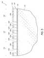
- a protective layer 170is deposited over the surface of the partially fabricated integrated circuit 100 .
- the protective layer 170is preferably also selectively definable.
- the protective layer 170is preferably photodefinable, e.g., formed of a photoresist, including any photoresist known in the art.
- the protective, photodefinable layer 170can be formed of a resist suitable for patterning by nano-imprint lithography.
- the photodefinable layer 170is patterned using, e.g., the same photolithographic technique used to pattern the photodefinable layer 120 .
- the layer 170is exposed to radiation through a reticle and then developed to expose elements the array region 102 of the partially fabricated integrated circuit 100 .
- some spacers or pairs of spacers 165are exposed, while some are protected by the protective layer 170 .
- some parts of the hard mask layer 130are exposed, while some parts are protected.
- elements in the interface areas 104 or periphery 106can also be patterned, thereby forming, for example, a void 174 in the periphery.
- spacers 165 in the array 102preferably have a pitch or element size smaller than the minimum pitch or resolution of the photolithographic technique used in forming it
- elements patterned in the layer 170preferably have a pitch or element size equal to or greater than the minimum pitch or resolution of the photolithographic technique used to form them.
- connections 172 to the spaces between the pitch multiplied spacers 165can be patterned. It will be appreciated that the connections 172 can be the ends of larger dimension elements 173 such as those used to pattern an interconnect in the periphery 106 or interface region 104 . The connections 172 can thus connect one or more mandrels 134 a to a larger mask element 173 and ultimately allow the formation of a relatively large interconnect connected to pitch-multiplied interconnects in the array 102 .
- spacers 165augment the dimensions of these elements, after removal of the protective layer 170 .
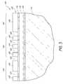
- parts of the first hard mask layer 130 and temporary layer 140 which are left exposed or unprotected by the protective layer 170are selectively removed, preferably by an anisotropic etch.
- the unprotected parts of the hard mask layer 130 and the temporary 140can be removed in a single step; that is, in situ in a single process chamber.
- the hard mask layer 130can be selectively removed using, e.g., a plasma etch containing HBr/CF 4
- the temporary layer 140can be selectively removed using, e.g., a SO 2 /O 2 plasma etch.
- the protective layer 170is then removed, e.g., by plasma ashing.
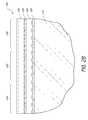
- the mandrels 134 a( FIG. 9A ) are removed, leaving free-standing, pitch multiplied spacers 165 in the array region 102 .
- the pitch of the spacers 165 and the spaces between the spacers 165are roughly half that of the photoresist lines 124 and spaces 122 ( FIG. 3 ) originally formed by photolithography.
- the photoresist lines 124had a pitch of about 200 nm
- spacers 165 having a pitch of about 100 nm or lesscan be formed.
- elements patterned in the periphery 106 or interface region 104are also transferred to the underlying layers, thereby forming, e.g., the void or opening 176 in the hard mask layer 130 and the temporary layer 140 .
- the pattern defined by the spacers 165 and the remaining parts of the first hard mask layer 130 and the temporary layer 140is transferred to the second hard mask layer 150 .
- the transferis preferably accomplished using an anisotropic etch, e.g., an etch using a fluorocarbon plasma, e.g., a CF 4 /O 2 /CH 2 F 2 -containing plasma etch.
- the substratecan subsequently be processed through the mask defined in the second hard mask layer 150 .
- the patterncan be transferred to the substrate 110 .
- FIG. 13it will be appreciated that, where the substrate 110 is etched, etching of the substrate 110 can remove the spacers 165 and the remaining parts of the layers 130 , 140 .
- the second hard mask layer 150is used as the primary mask for etching the substrate 110 .
- the spacers 165 and the remaining parts of the layers 130 , 140can be removed before or after processing of the substrate 110 .
- the hard mask layer 150can be removed after processing the substrate 110 .
- the substrate 110is etched using an anisotropic etch selective for the substrate 110 relative to at least the second hard mask layer 150 .
- a succession of different chemistriespreferably dry-etch chemistries, can be used to successively etch through these different materials, if a single chemistry is not sufficient to etch all the different materials.
- the composition of the substrate 110can depend upon, e.g., the electrical device to be formed.
- the pattern formed by the spacers 165 and then transferred to the second hard mask layer 150 and the substrate 110can define lines, e.g., interconnects for connecting electrical devices.
- the electrical devicesare arranged in an array, such as the electrical devices which form memory cells in the array region of a memory device.
- the connections 172FIG. 9B ) can advantageously define connections between larger features in the interface or periphery areas of an integrated circuit and pitch multiplied features, such as defined by the element 171 , in the array.
- the partially fabricated integrated circuit 100can be subjected to subsequent processing steps, including forming ancillary electrical devices and electrical interconnects, to form a completed integrated circuit, e.g., a memory chip.
- pitch multiplied patternstypically include closed loops, which are formed by spacers that are formed along the wall of a mandrel. Consequently, in non-damascene processes, where the spacers 165 , rather the space between the spacers 165 , are used to form conductive lines, additional processing steps are preferably used to cut off the ends of these loops, so that each loop forms two individual, non-connected lines. This can be accomplished, for example, by forming a protective mask around the parts of the lines to be maintained, while etching away the unprotected ends of the masks. A suitable method for cutting off the ends of the loops is disclosed in U.S.
- the spacers 165to define the location of insulating material, rather than conductive material, the step of cutting off the ends of the spacer loops can be avoided. For example, it is unnecessary to cut off the ends of spacers loops where the spaces, e.g., the spaces formerly occupied by the mandrels, between the spacers 165 determine the location and shape of interconnects.
- the spacers 165can be removed before processing the substrate 110 . Such removal may be beneficial, for example, where the spacers 165 are relatively tall and thin. Such spacers may not be structurally stable and may deform over the course of an etch of the 110 substrate, thereby introducing errors in the pattern etched into the substrate. As a result, removal of the spacers 165 and any remaining parts of the hard mask layer 130 or temporary layer 140 may advantageously stabilize the mask (defined in this example by the lower hard mask layer 150 ) through which the substrate 110 is processed.
- the pitch of the spacers 165can be more than doubled.
- the spacers 165can be further pitch multiplied by removing the mandrels 134 a , forming additional spacers around the spacers 165 , removing the spacers 165 , then forming another set of spacers around the spacers that were formerly around the spacers 165 , and so on.
- An exemplary method for further pitch multiplicationis discussed in U.S. Pat. No. 5,328,810 to Lowrey et al.
- the preferred embodimentscan be employed multiple times throughout an integrated circuit fabrication process to form pitch multiplied features in a plurality of layers or vertical levels, which may be vertically contiguous or non-contiguous and/or vertically separated.
- each of the individual levels to be patternedwould constitute a substrate 110 and the various layers 120 - 170 can formed over the individual level to be patterned.
- the particular composition and height of the various layers 120 - 170 discussed abovecan be varied depending upon a particular application.
- the thickness of the layer 150can be varied depending upon the identity of the substrate 110 , e.g., the chemical composition of the substrate, whether the substrate comprises single or multiple layers of material, the depth of features to be formed, etc., and the available etch chemistries.
- one or more layers of the layer 120 - 170can be omitted or more layers can be added.
- the pattern formed in the second hard mask layer 150can be transferred to one or more additional hard mask layers, to provide a hard mask with increased resistance to etches selective for the substrate 110 .
- processing through the mask layerscan involve subjecting layers underlying the mask layers to any semiconductor fabrication process.
- processingcan involve ion implantation, diffusion doping, depositing, oxidizing (particularly with use of a hard mask under the polymer mask), nitridizing, etc. through the mask layers and onto underlying layers.
- the mask layerscan be used as a stop or barrier for chemical mechanical polishing (CMP) or CMP can be performed on any of the layers to allow for both planarization and etching of the underlying layers, as discussed in U.S. patent application Ser. No. 11/216,477, filed Aug. 31, 2005, the entire disclosure of which is incorporated by reference herein.
- a methodfor integrated circuit fabrication.
- the methodcomprises patterning a first photoresist layer to form a photoresist pattern over a substrate.
- the photoresist patternis transferred to a hardmask layer underlying the photoresist layer and a temporary layer underlying the hardmask layer. Spacers are formed on sidewalls of elements in the patterned hardmask and temporary layers.
- a second photoresist layeris deposited over the spacers and the patterned hardmask and temporary layers.
- the second photoresist layeris patterned to expose some parts of the patterned hardmask and temporary layers and to expose some of the spacers, while leaving photoresist directly over other parts of the patterned hardmask and temporary layers and over others of the spacers.
- the exposed parts of the patterned hardmask and temporary layersare subsequently preferentially removed.
- the second photoresist layeris preferentially removed.
- a methodfor forming an integrated circuit.
- the methodcomprises patterning a selectively definable layer to simultaneously define array mask elements in an array region and periphery mask elements in a periphery region of a partially fabricated integrated circuit. Pitch multiplication is subsequently performed in the array region to form a plurality of free-standing spacers. A pattern defined at least partly by the free-standing spacers and the periphery mask elements are simultaneously transferred to a substrate.
- a methodfor fabricating an integrated circuit.
- the methodcomprises providing a substrate with an overlying photoresist layer.
- the photoresist layeris patterned using a photolithographic technique, thereby forming a photoresist pattern comprising photoresist material separated by voids.
- the photoresist material and voidsextend over an array region and a periphery region of the integrated circuit.
- the photoresist patternis transferred to an underlying temporary layer to form a temporary layer pattern.
- the elements in the temporary layer patternare subsequently shrunk in both the array and the periphery regions.
- a blanket layer of spacer materialis deposited over the temporary layer elements.
- the blanket layeris etched to form spacers at sides of the temporary layer elements.
- a partially fabricated integrated circuitcomprises a plurality of mask elements overlying a hard mask layer.
- the hard mask layeroverlies a substrate.
- Spacersare disposed on sidewalls of the mask elements.
- a protective layerdirectly overlies some of the spacers and some of the mask elements. The protective layer also leaves others of the spacers and others of the mask elements exposed.
- a partially formed integrated circuitcomprises a plurality of pairs of spacers over a substrate. Spacers constituting each pair of spacers are separated by a selectively etchable material. A patterned photoresist layer overlies some of the pairs of spacers. Photoresist overlies at least some spacers in a periphery or interface region of the partially fabricated integrated circuit, while spacers in an array region of the partially fabricated integrated circuit are exposed.
- a partially formed integrated circuitcomprises a plurality of pairs of free-standing spacers disposed over an array region of the partially fabricated integrated circuit.
- An other plurality of other pairs of spacersis disposed on the same level as the plurality of pairs of spacers.
- Spacers constituting each of the other pairs of spacersare disposed on sidewalls of a temporary material selectively etchable relative to the other pairs of spacers.
- the temporary materialis provided with one or more openings.
Landscapes
- Engineering & Computer Science (AREA)
- Manufacturing & Machinery (AREA)
- Microelectronics & Electronic Packaging (AREA)
- Power Engineering (AREA)
- Condensed Matter Physics & Semiconductors (AREA)
- General Physics & Mathematics (AREA)
- Physics & Mathematics (AREA)
- Computer Hardware Design (AREA)
- Chemical & Material Sciences (AREA)
- Inorganic Chemistry (AREA)
- Internal Circuitry In Semiconductor Integrated Circuit Devices (AREA)
- Semiconductor Memories (AREA)
- Drying Of Semiconductors (AREA)
- Non-Volatile Memory (AREA)
- Exposure Of Semiconductors, Excluding Electron Or Ion Beam Exposure (AREA)
Abstract
Description
- This application is a divisional of U.S. patent application Ser. No. 13/198,581 to Fischer et al., EFFICIENT PITCH MULTIPLICATION PROCESS, filed Aug. 4, 2011, which is a divisional of U.S. patent application Ser. No. 12/687,005 to Fischer et al., EFFICIENT PITCH MULTIPLICATION PROCESS, filed Jan. 13, 2010 (now U.S. Pat. No. 8,012,674), which is a continuation of U.S. patent application Ser. No. 11/521,851 to Fischer et al., EFFICIENT PITCH MULTIPLICATION PROCESS, filed Sep. 14, 2006 (now U.S. Pat. No. 7,666,578).
- This application is related to the following: U.S. patent application Ser. No. 10/934,778 to Abatchev et al., Method for Integrated Circuit Fabrication Using Pitch Multiplication, filed Sep. 2, 2004; U.S. patent application Ser. No. 10/931,771 to Tran et al., Methods for Increased Photo Alignment Margins, filed Aug. 31, 2004; U.S. patent application Ser. No. 11/214,544 to Tran et al., Pitch Reduced Patterns Relative To Photolithography Features, filed Aug. 29, 2005; U.S. patent application Ser. No. 11/366,212 to Werner Juengling, Process Flow for Vertical Transistor Arrays, filed Mar. 2, 2006; and U.S. patent application Ser. No. 11/367,020 to Werner Juengling, Masking Process For Simultaneously Patterning Separate Regions, filed Mar. 2, 2006. The entireties of each of these references are incorporated by reference herein.
- 1. Field of the Invention
- This invention relates generally to integrated circuit fabrication and, more particularly, to masking techniques.
- 2. Description of the Related Art
- As a consequence of many factors, including demand for increased portability, computing power, memory capacity and energy efficiency, integrated circuits are continuously being reduced in size. The sizes of the constituent features that form the integrated circuits, e.g., electrical devices and interconnect lines, are also constantly being decreased to facilitate this size reduction.
- The trend of decreasing feature size is evident, for example, in memory circuits or devices such as dynamic random access memories (DRAMs), flash memory, static random access memories (SRAMs), ferroelectric (FE) memories, etc. To take one example, DRAM typically comprises millions of identical circuit elements, known as memory cells. A DRAM memory cell typically consists of two electrical devices: a storage capacitor and an access field effect transistor. Each memory cell is an addressable location that can store one bit (binary digit) of data. A bit can be written to a cell through the transistor and can be read by sensing charge in the capacitor. By decreasing the sizes of the electrical devices that constitute a memory cell and the sizes of the conducting lines that access the memory cells, the memory devices can be made smaller. Additionally, storage capacities can be increased by fitting more memory cells on a given area in the memory devices. Other memory designs can integrate access and storage devices or omit access devices (e.g., cross-point MRAM, PCRAM, etc.).
- The continual reduction in feature sizes places ever greater demands on the techniques used to form the features. For example, photolithography is commonly used to pattern features, such as conductive lines. The concept of pitch can be used to describe the sizes of these features. Pitch is defined as the distance between an identical point in two neighboring features of a repeating pattern. These features are typically defined by spaces between adjacent features, which spaces are typically filled by a material, such as an insulator. As a result, pitch can be viewed as the sum of the width of a feature and of the width of the space on one side of the feature separating that feature from a neighboring feature. However, due to factors such as optics and light or radiation wavelength, photolithography techniques each have a minimum pitch below which a particular photolithographic technique cannot reliably form features. Thus, the minimum pitch of a photolithographic technique is an obstacle to continued feature size reduction.
- “Pitch doubling” or “pitch multiplication” is one proposed method for extending the capabilities of photolithographic techniques beyond their minimum pitch. A pitch multiplication method is illustrated in
FIGS. 1A-1F and described in U.S. Pat. No. 5,328,810, issued to Lowrey et al., the entire disclosure of which is incorporated herein by reference. With reference toFIG. 1A , a pattern oflines 10 is photolithographically formed in a photoresist layer, which overlies alayer 20 of an expendable material, which in turn overlies asubstrate 30. As shown inFIG. 1B , the pattern is then transferred using an etch (preferably an anisotropic etch) to thelayer 20, thereby forming placeholders, or mandrels,40. Thephotoresist lines 10 can be stripped and themandrels 40 can be isotropically etched to increase the distance between neighboringmandrels 40, as shown inFIG. 1C . Alayer 50 of spacer material is subsequently deposited over themandrels 40, as shown inFIG. 1D . Spacers60 (FIG. 1E ), i.e., the material extending or originally formed extending from sidewalls of another material, are then formed on the sides of themandrels 40. The spacer formation is accomplished by preferentially etching the spacer material from thehorizontal surfaces FIG. 1E . Theremaining mandrels 40 are then removed, leaving behind only thespacers 60, which together act as a mask for patterning, as shown inFIG. 1F . Thus, where a given pitch previously included a pattern defining one mask element and one space, the same width now includes two mask elements and two spaces, with the spaces defined by, e.g., thespacers 60. As a result, the smallest feature size that can be formed with a photolithographic technique is effectively decreased. - While the pitch is actually halved in the example above, this reduction in pitch is conventionally referred to as pitch “doubling,” or, more generally, pitch “multiplication.” Thus, conventionally, “multiplication” of pitch by a certain factor actually involves reducing the pitch by that factor. The conventional terminology is retained herein.
- Because the
layer 50 of spacer material typically has a single thickness90 (seeFIGS. 1D and 1E ) and because the sizes of the mask elements formed by thespacers 60 usually correspond to thatthickness 90, pitch doubling typically produces mask elements of only one width. Circuits, however, generally employ features of different sizes. For example, random access memory circuits typically contain arrays of memory cells located in one part of the circuits and logic circuits located in the so-called “periphery.” In the arrays, the memory cells are typically connected by conductive lines and, in the periphery, the conductive lines typically contact interconnects in the periphery or landing pads for connecting arrays to logic. Peripheral features such as peripheral interconnects and landing pads, however, can be larger than the conductive lines in the array. In addition, electrical devices in the periphery, including peripheral transistors, can be larger than the electrical devices in the array. Moreover, even if peripheral features can be formed with the same pitch as features in the array, because mask patterns formed by pitch multiplication may be limited to those that are formed along the sidewalls of patterned photoresist, it is challenging to employ pitch multiplication while achieving the flexibility, e.g., geometric flexibility, required to define some features. - Accordingly, there is a need for methods of forming features of different sizes, especially where some features are formed below the minimum pitch of a photolithographic technique, and especially in conjunction with pitch multiplication.
- The invention will be better understood from the Detailed Description of the Preferred Embodiments and from the appended drawings, which are meant to illustrate and not to limit the invention, and wherein:
FIGS. 1A-1F are schematic, cross-sectional side views of a sequence of masking patterns for forming conductive lines, in accordance with a prior art pitch doubling method;FIG. 2A is a schematic top plan view of a partially formed integrated circuit, in accordance with preferred embodiments of the invention;FIG. 2B is a schematic cross-sectional side view of the partially formed integrated circuit ofFIG. 2A , in accordance with preferred embodiments of the invention;FIG. 3 is a schematic cross-sectional side view of the partially formed integrated circuit ofFIGS. 2A-2B after forming lines in a photoresist layer, in accordance with preferred embodiments of the invention;FIG. 4 is a schematic cross-sectional side view of the partially formed integrated circuit ofFIG. 3 after transferring the pattern in the photoresist layer to underlying hard mask and temporary layers and removing the photoresist layer, in accordance with preferred embodiments of the invention;FIG. 5 is a schematic, cross-sectional side view of the partially formed integrated circuit ofFIG. 4 after performing a trim etch to widen spaces between mask elements, in accordance with preferred embodiments of the invention;FIG. 6 is a schematic, cross-sectional side view of the partially formed integrated circuit ofFIG. 5 after depositing a layer of a spacer material, in accordance with preferred embodiments of the invention;FIGS. 7A-7B are schematic, cross-sectional side and top plan views of the partially formed integrated circuit ofFIG. 6 after performing a spacer etch, in accordance with preferred embodiments of the invention;FIG. 8 is a schematic, cross-sectional side view of the partially formed integrated circuit ofFIGS. 7A-7B after depositing a layer of protective material, in accordance with preferred embodiments of the invention;FIGS. 9A-9B are schematic, cross-sectional side and top plan views of the partially formed integrated circuit ofFIG. 8 after patterning the protective layer to expose mask elements in the array region and other selected areas of the partially formed integrated circuit, in accordance with preferred embodiments of the invention;FIGS. 10A-10B are schematic, cross-sectional side and top plan views of the partially formed integrated circuit ofFIGS. 9A-9B after removing hard mask and temporary layer material in regions exposed by the patterned protective layer, thereby leaving a pattern of free-standing spacers, and subsequent removal of the protective layer, in accordance with preferred embodiments of the invention;FIG. 11 is a schematic, cross-sectional side view of the partially formed integrated circuit ofFIGS. 10A-10B after etching the pattern of pitch multiplied and non-pitch multiplied mask elements into an underlying hard mask layer, in accordance with preferred embodiments of the invention;FIG. 12 is a schematic, cross-sectional side view of the partially formed integrated circuit ofFIG. 11 after transferring the pattern of pitch multiplied and non-pitch multiplied mask elements to the underlying substrate, in accordance with preferred embodiments of the invention;FIG. 13 is a schematic, cross-sectional side view of the partially formed integrated circuit ofFIG. 12 after removing mask elements overlying the substrate, in accordance with other preferred embodiments of the invention; andFIG. 14 is a schematic, cross-sectional side view of the partially formed integrated circuit ofFIG. 12 or13 after removing all mask elements overlying the substrate, in accordance with other preferred embodiments of the invention.- Because of the difference in size between pitch multiplied features and larger features such as non-pitch multiplied features, connecting pitch multiplied features to the larger features can be difficult. For example, the pitch multiplied features are typically too small and/or closely spaced to reliably contact features such as contact plugs or larger sized interconnects. Shorting or other misalignments can occur because of the small size and/or close spacing of the pitch multiplied features. Various strategies have been proposed for forming pitch multiplied and non-pitch multiplied features. Exemplary methods for forming pitch multiplied and non-pitch multiplied features are described in U.S. patent application Ser. No. 10/934,778 to Abatchev et al. and U.S. patent application Ser. No. 10/931,771 to Tran et al., both of which are assigned to the assignee of the present application. The entire disclosures of each of these references are incorporated by reference herein.
- In addition to difficulties with forming and connecting pitch multiplied and non-pitch multiplied features, the process flows can be complicated, due to the need to form and overlay features of different sizes. For example, the pitch multiplied features can be formed separately from the larger sized features, thereby requiring multiple mask formation and mask consolidation steps. It will be appreciated that each additional step in a process flow can undesirably add to the complexity and expense of a process flow. Moreover, each additional step has the possibility of introducing misalignments and etch and pattern transfer complications and other errors which can cause undesirable variations in process results.
- In view of these difficulties, preferred embodiments of the invention allow for the formation and connection of pitch multiplied and non-pitch multiplied features using an advantageously simple process flow. Preferably, parts of a selectively definable layer (e.g., a photoresist layer) corresponding to the array, interface and periphery areas of an integrated circuit are simultaneously patterned. Pitch multiplication is used to form pitch multiplied spacers in the array region. At least some parts of the interface and the periphery regions are protected using a protective material while other parts are etched and free-standing spacers are formed in the array region. The protective material is then removed and a pattern including spacers in the array region and features in the interface and the periphery regions are then transferred to a hard mask layer. The hard mask layer can be used to pattern an underlying substrate.
- Advantageously, processing according to the preferred embodiments allows for the formation and connection of pitch-multiplied to non-pitch multiplied features using relatively few process steps. The relatively small number of steps can improve the uniformity of process results. Non-uniformities introduced by additional pattern formation and pattern transfer steps can be reduced. Moreover, as discussed herein, because connections of non-pitch multiplied mask elements to pitch multiplied mask elements can be formed simultaneously on the same vertical level with the non-pitch multiplied mask elements, defects caused by misaligning separately formed mask elements can be reduced. Thus, connections to pitch multiplied features can be formed more reliably, thereby reducing the possibility of shorts and poorly connected pitch-multiplied features. In addition, the relatively low number of process steps advantageously allows for the fabrication of integrated circuits with high throughput and relatively low cost.
- Reference will now be made to the Figures, wherein like numerals refer to like parts throughout. It will be appreciated that these Figures are not necessarily drawn to scale.
- Initially, a stack of layers suitable for forming a pattern in a hard mask layer is formed.
- With reference to
FIG. 2A , a top view of a partially fabricated integratedcircuit 100 is shown. While the preferred embodiments can be used to form any integrated circuit, they are particularly advantageously applied to form devices having arrays of electrical devices, including memory cell arrays for volatile and non-volatile memory devices such as DRAM, ROM or flash memory, including NAND flash memory, or integrated circuits having logic or gate arrays. The logic array can be a field programmable gate array (FPGA) having a core array similar to a memory array and a periphery with supporting logics. As a result, theintegrated circuit 100 can be, e.g., a memory chip or a processor, which can include both a logic array and embedded memory, or any other integrated circuit having arrays of features, such as a logic or a gate array. - With continued reference to
FIG. 2A , acentral region 102, the array region or simply “array,” is surrounded by ainterface region 104, which is surrounded by aperipheral region 106, also referred to as the “periphery.” It will be appreciated that, after fabrication of theintegrated circuit 100 is completed, thearray 102 will typically be densely populated with conducting lines and electrical devices such as transistors and capacitors. In a memory device, the electrical devices form a plurality of memory cells, which are typically arranged in a regular grid pattern at the intersection of word lines and bit lines. Desirably, pitch multiplication can be used to form features such as rows and/or columns of transistors and capacitors in thearray 102, as discussed below. - On the other hand, the
periphery 106 typically comprises features larger than those in thearray 102. Conventional photolithography, rather than pitch multiplication, is preferably used to pattern features, such as logic circuitry, in theperiphery 106, because the geometric complexity of logic circuits located in theperiphery 106 makes using pitch multiplication difficult. For example, features in theperiphery 106 typically do not have the repeating regularity of features typical in thearray 102. Moreover, the logic area need not be as dense as thearray regions 102, such that pitch multiplication in the logic area is unnecessary. In contrast, the regular grid typical of array patterns is conducive to pitch multiplication. In addition, some devices in the periphery require larger geometries due to electrical constraints, thereby making pitch multiplication less advantageous than conventional photolithography for such devices. - The
interface region 104 can contain both array and periphery features. For example, theinterface region 104 can serve as a transition from thearray 102 to theperiphery 106 and allow contact between features in thearray 102 and features in theperiphery 106. - While schematically illustrated as concentric regions, it will be appreciated by the skilled artisan that the relative positions, and the number of
array 102,interface 104 andperiphery 106 regions in theintegrated circuit 100 may vary from that depicted. For example, in some areas of theintegrated circuit 100, theinterface 104 andperiphery 106 regions may be disposed directly with either side of thearray region 102, as illustrated in some of the figures below. Moreover, while certain specific characteristics of these regions have been noted above and clear demarcations between the regions have been illustrated for ease of discussion, in some arrangements, two or more of the regions can overlap. FIG. 2B shows a cross-sectional side view of the partially formedintegrated circuit 100. Various masking layers120-150 are preferably provided above asubstrate 110. The layers120-150 will be etched to form a mask for patterning thesubstrate 110, as discussed below.- The materials for the layers120-150 overlying the
substrate 110 are preferably chosen based upon consideration of the chemistry and process conditions for the various pattern forming and pattern transferring steps discussed herein. Because the layers between a topmost selectively definable (e.g., photodefinable)layer 120 and thesubstrate 110 preferably function to transfer a pattern derived from the selectivelydefinable layer 120 to thesubstrate 110, the layers130-150 between the selectivelydefinable layer 120 and thesubstrate 110 are preferably chosen so that they can be selectively etched relative to other exposed materials. It will be appreciated that a material is considered selectively, or preferentially, etched when the etch rate for that material is at least about 2-3 times greater, preferably at least about 10 times greater, more preferably at least about 20 times greater and, most preferably, at least about 50 times greater than that for surrounding materials. Because a goal of the layers120-140 overlying a secondhard mask layer 150 is to allow well-defined patterns to be formed in the secondhard mask layer 150, it will be appreciated that one or more of the layers120-140 can be omitted or substituted if suitable other materials, chemistries and/or process conditions are used. - In the illustrated embodiment, the selectively
definable layer 120 overlies a first hard mask, or etch stop,layer 130, which overlies atemporary layer 140, which overlies the second hard mask, or etch stop,layer 150, which overlies thesubstrate 110 to be processed (e.g., etched) through a mask. Preferably, the mask through which thesubstrate 110 is processed is formed in the secondhard mask layer 150. - With continued reference to
FIG. 2B , the selectivelydefinable layer 120 is preferably photodefinable, e.g., formed of a photoresist, including any photoresist known in the art. For example, the photoresist can be any photoresist compatible with 157 nm, 193 nm, 248 nm or 365 nm wavelength systems, 193 nm wavelength immersion systems, extreme ultraviolet systems (including 13.7 nm wavelength systems) or electron beam lithographic systems. In addition, maskless lithography, or maskless photolithography, can be used to define thephotodefinable layer 120. Examples of preferred photoresist materials include argon fluoride (ArF) sensitive photoresist, i.e., photoresist suitable for use with an ArF light source, and krypton fluoride (KrF) sensitive photoresist, i.e., photoresist suitable for use with a KrF light source. ArF photoresists are preferably used with photolithography systems utilizing relatively short wavelength light, e.g., 193 nm. KrF photoresists are preferably used with longer wavelength photolithography systems, such as 248 nm systems. In other embodiments, thelayer 120 and any subsequent resist layers can be formed of a resist that can be patterned by nano-imprint lithography, e.g., by using a mold or mechanical force to pattern the resist. - The material for the first
hard mask layer 130 preferably comprises an inorganic material. Exemplary materials include silicon oxide (SiO2), silicon or a dielectric anti-reflective coating (DARC), such as a silicon-rich silicon oxynitride. In the illustrated embodiment, the firsthard mask layer 130 is a dielectric anti-reflective coating (DARC). Using DARCs for the firsthard mask layer 130 can be particularly advantageous for forming patterns having pitches near the resolution limits of a photolithographic technique. The DARCs can enhance resolution by minimizing light reflections, thus increasing the precision with which photolithography can define the edges of a pattern. - The
temporary layer 140 is preferably formed of amorphous carbon, which offers very high etch selectivity relative to the preferred hard mask materials. More preferably, the amorphous carbon is a form of amorphous carbon that is highly transparent (so-called “transparent carbon”) to light and that offers improvements for photo-alignment by being transparent to the wavelengths of light used for such alignment. Deposition techniques for forming such transparent carbon can be found in A. Helmbold, D. Meissner, Thin Solid Films, 283 (1996) 196-203, the entire disclosure of which is incorporated herein by reference. - The second
hard mask layer 150 can be formed of a hard mask material suitable for etching theunderlying substrate 110 and which can be selectively etched relative to exposed overlying materials, such as spacers165 (FIG. 11 ). For example, in some embodiments where the spacer material (FIG. 11 ) is silicon oxide or silicon, the hard mask material can be silicon nitride. In other embodiments where the spacer material is silicon nitride or silicon, the hard mask material can be silicon oxide. In the illustrated embodiment, the hard mask material is a nitride, preferably silicon nitride. - It will be appreciated that the
substrate 110 can include a layer of a single material, a plurality of layers of different materials, a layer or layers having regions of different materials or structures in them, etc. These materials can include semiconductors, insulators, conductors, or combinations thereof. For example, the substrate can comprise doped polysilicon, an electrical device active area, a silicide, or a metal layer, such as a tungsten, aluminum or copper layer, or combinations thereof. In some embodiments, the mask elements discussed below can directly correspond to the desired placement of conductive features, such as interconnects or landing pads, in the substrate. In the illustrated embodiment, the upper portion of thesubstrate 110 includes an insulator and the location of mask elements can correspond to the desired location of insulators, such as in damascene metallization. Examples of structures formed in the substrate include interconnects, gate stacks and shallow trench isolation structures. - The layers120-150 discussed herein can be formed by various methods. For example, spin-on-coating processes can be used to form photodefinable layers. Various vapor deposition processes, such as chemical vapor deposition, can be used to form hard mask layers. Preferably, a low temperature chemical vapor deposition (CVD) process is used to deposit the hard mask layers or any other materials, e.g., spacer material, over the
temporary layer 140, especially in cases where thetemporary layer 140 is formed of amorphous carbon. - The amorphous carbon for the
temporary layer 140 can be formed by chemical vapor deposition using a hydrocarbon compound, or mixtures of such compounds, as carbon precursors. Exemplary precursors include propylene, propyne, propane, butane, butylene, butadiene and acetelyne. A suitable method for forming amorphous carbon layers is described in U.S. Pat. No. 6,573,030 B1, issued to Fairbairn et al. on Jun. 3, 2003, the entire disclosure of which is incorporated herein by reference. In addition, the amorphous carbon may be doped. A suitable method for forming doped amorphous carbon is described in U.S. patent application Ser. No. 10/652,174 to Yin et al., the entire disclosure of which is incorporated herein by reference. - Next, patterns are formed and transferred to the
hard mask layer 150. - It will be appreciated that in any of the steps described herein, transferring a pattern from an overlying level to an underlying level involves forming integrated circuit features or mask elements in the underlying level that generally correspond to mask elements in the overlying level. For example, the path of lines in the underlying level will generally follow the path of lines in the overlying level and the location of other elements or features in the underlying level will correspond to the location of similar elements or features in the overlying level. The precise shapes and sizes of elements or features can vary from the overlying level to the underlying level, however. For example, depending upon etch chemistries and conditions, the sizes of and relative spacing between the elements or features forming the transferred pattern can be enlarged or diminished relative to the pattern on the overlying level, while still resembling the same initial “pattern,” as can be seen from the example of shrinking the first resist mask in the embodiments described below. Thus, even with some changes in the dimensions of elements or features, the transferred pattern is still considered to be the same pattern as the initial pattern. In contrast, forming spacers around mask elements can form new (pitch multiplied) patterns.
- With reference to
FIG. 3 , a pattern comprising spaces ortrenches array elements 124,interface elements 126 andperiphery element 128, is formed in thephotodefinable layer 120. Theelements trenches layer 120 is exposed to radiation through a reticle and then developed. After being developed, the remaining photodefinable material, photoresist in the illustrated embodiment, forms the illustratedelements array elements 124 are lines. - The pitch of the
lines 124 is equal to the sum of the width of aline 124 and the width of a neighboringspace 122. To minimize the critical dimensions of elements formed using this pattern oflines 124 andspaces 122, the pitch can be at or near the limits of the photolithographic technique used to pattern thephotodefinable layer 120. For example, for photolithography utilizing 248 nm light, the pitch of thelines 124 can be about 100 nm. Thus, the pitch may be at the minimum pitch of the photolithographic technique and the spacer pattern discussed below can advantageously have a pitch below the minimum pitch of the photolithographic technique. Alternatively, because the margin of error for position and element size typically increases as the limits of a photolithographic technique are approached, thelines 124 can be formed having larger element sizes, e.g., for a pitch of about 200 nm, to minimize errors in the position and sizes of thelines 124. - With reference to
FIG. 4 , the pattern in thephotodefinable layer 120 is transferred to thehard mask layer 130 and thetemporary layer 140 to allow for deposition of alayer 160 of spacer material (FIG. 6 ). It has been found that the temperatures used for spacer material deposition are typically too high for photoresist to withstand. Thus, the pattern is preferably transferred from thephotodefinable layer 120 to the firsthard mask layer 130 and thetemporary layer 140, which are formed of materials that can withstand the process conditions for spacer material deposition and etch, discussed below. In addition to having higher heat resistance than photoresist, the material forming thetemporary layer 140 is preferably selected such that it can be selectively removed relative to the material for the spacers165 (FIG. 10 ) and for the underlying secondhard mask layer 150. As noted above, thelayer 140 is preferably formed of amorphous carbon and, more preferably, transparent carbon. - The pattern transfer may be accomplished in a single step; that is, in situ in a single process chamber. The transfer is preferably accomplished using anisotropic etches. Preferred etch chemistries include an etch using fluorocarbon plasma, e.g., plasma generated from HBr/CF4, to etch the first
hard mask layer 130 and an oxygen-containing plasma, e.g., a SO2/O2plasma, to etch thetemporary layer 140. The etches selectively etch the firsthard mask layer 130 relative to thephotodefinable layer 120 and then continue through thetemporary layer 140, stopping at the secondhard mask layer 150. Part of thephotodefinable layer 120 may be etched during the pattern transfer. Any remaining resist forming thephotodefinable layer 120 can subsequently be separately removed by various processes known by the skilled artisan, including, e.g., by plasma ashing. - With reference to
FIGS. 4 and 5 ,spaces 132,133 betweenarray elements 134,interface elements 136 andperiphery elements 138 are preferably widened by etching theelements spaces elements elements elements FIG. 7A ) having a desired spacing, as will be appreciated from the discussion below. For example, the width of theelements photodefinable layer 120. In addition, the etch can smooth the edges of theelements elements spaces elements elements elements FIG. 3 ) in thephotodefinable layer 120 can be subjected to a trim etch before transferring the pattern from thephotodefinable layer 120 to the firsthard mask layer 130, to form elements of desired size in thehard mask layer 130 andtemporary layer 140. - With reference to
FIG. 6 , alayer 160 of spacer material is preferably blanket deposited conformally over exposed surfaces, including exposed top surfaces and sidewalls of the hard mask layers130,150 and the sidewalls of thetemporary layer 140. The spacer material can be any material that can act as a mask for transferring a pattern to the underlyinghard mask layer 150. The spacer material preferably: 1) can be deposited with good step coverage; 2) can be deposited at a temperature compatible with other materials in the partially fabricated integratedcircuit 100; and 3) can be selectively and anisotropically etched relative to thetemporary layer 140 and the first and second hard mask layers130,150. Preferred materials include silicon (e.g., amorphous silicon), silicon oxides and silicon nitrides. In the illustrated embodiment, the spacer material is silicon oxide, which provides particular advantages in combination with other selected materials of the masking stack. - Preferred methods for spacer material deposition include chemical vapor deposition and atomic layer deposition. The thickness of the
layer 160 is preferably determined based upon the desired width of the spacers165 (FIG. 10 ). For example, in the illustrated embodiment, thelayer 160 is preferably deposited to a thickness of about 20-80 nm and, more preferably, about 40-60 nm. Preferably, the step coverage is about 80% or greater and, more preferably, about 90% or greater. - With reference to
FIG. 7A , the siliconoxide spacer layer 160 is subjected to an anisotropic etch to remove spacer material fromhorizontal surfaces 166 of the partially formedintegrated circuit 100. Such an etch, also known as a spacer etch, can be performed on an oxide material using a biased fluorocarbon plasma, e.g., containing CF4/CHF3, C4F8/CH2F2or CHF3/Ar plasma, or with a purely physical sputter etch (e.g., an Ar sputter etch). The spacer etch defines pairs ofspacers 165 aroundmandrels 134aandelements FIG. 7B shows a top plan view of the partially formedintegrated circuit 100 ofFIG. 7A . As can be seen, themandrels 134acan have various shapes, in addition to being the shape of a line. As noted above, in the illustrated embodiment, the upper part of thesubstrate 110 is an insulator and the pattern of thespacers 165 correspond to the desired pattern of insulator to be formed in thesubstrate 110. Consequently, open space between thespacers 165 preferably corresponds to the desired placement of conductors, such as damascene conductive interconnects, in thesubstrate 110. For example, anymandrels 134awhich are later removed (FIGS. 10A-10B ), can have locations corresponding to the locations of later-formed interconnects. In such cases, somemandrels 134acan have widenedportions 137 which can be used to form landing pads for electrically connecting interconnects formed using themandrels 134awith electrical features on other vertical levels.- With reference to
FIG. 8 , aprotective layer 170 is deposited over the surface of the partially fabricated integratedcircuit 100. Theprotective layer 170 is preferably also selectively definable. As with the selectivelydefinable layer 120, theprotective layer 170 is preferably photodefinable, e.g., formed of a photoresist, including any photoresist known in the art. In addition, in other embodiments, the protective,photodefinable layer 170 can be formed of a resist suitable for patterning by nano-imprint lithography. - With reference to
FIG. 9A , thephotodefinable layer 170 is patterned using, e.g., the same photolithographic technique used to pattern thephotodefinable layer 120. Preferably, thelayer 170 is exposed to radiation through a reticle and then developed to expose elements thearray region 102 of the partially fabricated integratedcircuit 100. Thus, some spacers or pairs ofspacers 165 are exposed, while some are protected by theprotective layer 170. In addition, some parts of thehard mask layer 130 are exposed, while some parts are protected. - In addition, elements in the
interface areas 104 orperiphery 106 can also be patterned, thereby forming, for example, a void174 in the periphery. It will be appreciated that while thespacers 165 in thearray 102 preferably have a pitch or element size smaller than the minimum pitch or resolution of the photolithographic technique used in forming it, elements patterned in thelayer 170 preferably have a pitch or element size equal to or greater than the minimum pitch or resolution of the photolithographic technique used to form them. - With reference to
FIG. 9B ,connections 172 to the spaces between the pitch multipliedspacers 165 can be patterned. It will be appreciated that theconnections 172 can be the ends oflarger dimension elements 173 such as those used to pattern an interconnect in theperiphery 106 orinterface region 104. Theconnections 172 can thus connect one ormore mandrels 134ato alarger mask element 173 and ultimately allow the formation of a relatively large interconnect connected to pitch-multiplied interconnects in thearray 102. - It will be appreciated that some elements of the partially fabricated integrated
circuit 100 remain protected by thelayer 170. In such cases,spacers 165 augment the dimensions of these elements, after removal of theprotective layer 170. - With reference to
FIGS. 10A-10B , parts of the firsthard mask layer 130 andtemporary layer 140 which are left exposed or unprotected by theprotective layer 170 are selectively removed, preferably by an anisotropic etch. Advantageously, the unprotected parts of thehard mask layer 130 and the temporary140 can be removed in a single step; that is, in situ in a single process chamber. Thehard mask layer 130 can be selectively removed using, e.g., a plasma etch containing HBr/CF4, and thetemporary layer 140 can be selectively removed using, e.g., a SO2/O2plasma etch. Theprotective layer 170 is then removed, e.g., by plasma ashing. - Thus, the
mandrels 134a(FIG. 9A ) are removed, leaving free-standing, pitch multiplied spacers165 in thearray region 102. In the illustrated embodiment, the pitch of thespacers 165 and the spaces between thespacers 165 are roughly half that of thephotoresist lines 124 and spaces122 (FIG. 3 ) originally formed by photolithography. For example, where thephotoresist lines 124 had a pitch of about 200 nm,spacers 165 having a pitch of about 100 nm or less can be formed. In addition, elements patterned in theperiphery 106 orinterface region 104 are also transferred to the underlying layers, thereby forming, e.g., the void oropening 176 in thehard mask layer 130 and thetemporary layer 140. - With reference to
FIG. 11 , the pattern defined by thespacers 165 and the remaining parts of the firsthard mask layer 130 and thetemporary layer 140 is transferred to the secondhard mask layer 150. The transfer is preferably accomplished using an anisotropic etch, e.g., an etch using a fluorocarbon plasma, e.g., a CF4/O2/CH2F2-containing plasma etch. - The substrate can subsequently be processed through the mask defined in the second
hard mask layer 150. For example, with reference toFIG. 12 , the pattern can be transferred to thesubstrate 110. With reference toFIG. 13 , it will be appreciated that, where thesubstrate 110 is etched, etching of thesubstrate 110 can remove thespacers 165 and the remaining parts of thelayers hard mask layer 150 is used as the primary mask for etching thesubstrate 110. In other embodiments, thespacers 165 and the remaining parts of thelayers substrate 110. With reference toFIG. 14 , thehard mask layer 150 can be removed after processing thesubstrate 110. - Preferably, the
substrate 110 is etched using an anisotropic etch selective for thesubstrate 110 relative to at least the secondhard mask layer 150. It will be appreciated that where thesubstrate 110 comprises different materials, e.g., layers of different materials, a succession of different chemistries, preferably dry-etch chemistries, can be used to successively etch through these different materials, if a single chemistry is not sufficient to etch all the different materials. The composition of thesubstrate 110 can depend upon, e.g., the electrical device to be formed. - It will be appreciated that the pattern formed by the
spacers 165 and then transferred to the secondhard mask layer 150 and thesubstrate 110 can define lines, e.g., interconnects for connecting electrical devices. Preferably, the electrical devices are arranged in an array, such as the electrical devices which form memory cells in the array region of a memory device. The connections172 (FIG. 9B ) can advantageously define connections between larger features in the interface or periphery areas of an integrated circuit and pitch multiplied features, such as defined by theelement 171, in the array. After the lines are formed, the partially fabricated integratedcircuit 100 can be subjected to subsequent processing steps, including forming ancillary electrical devices and electrical interconnects, to form a completed integrated circuit, e.g., a memory chip. - It will be appreciated that various modifications of the illustrated embodiments are possible. For example, pitch multiplied patterns typically include closed loops, which are formed by spacers that are formed along the wall of a mandrel. Consequently, in non-damascene processes, where the
spacers 165, rather the space between thespacers 165, are used to form conductive lines, additional processing steps are preferably used to cut off the ends of these loops, so that each loop forms two individual, non-connected lines. This can be accomplished, for example, by forming a protective mask around the parts of the lines to be maintained, while etching away the unprotected ends of the masks. A suitable method for cutting off the ends of the loops is disclosed in U.S. patent application Ser. No. 10/931,771 to Tran et al., filed Aug. 31, 2004, the entire disclosure of which is incorporated be reference herein. Advantageously, however, by using thespacers 165 to define the location of insulating material, rather than conductive material, the step of cutting off the ends of the spacer loops can be avoided. For example, it is unnecessary to cut off the ends of spacers loops where the spaces, e.g., the spaces formerly occupied by the mandrels, between thespacers 165 determine the location and shape of interconnects. - Also, in some cases, the
spacers 165 can be removed before processing thesubstrate 110. Such removal may be beneficial, for example, where thespacers 165 are relatively tall and thin. Such spacers may not be structurally stable and may deform over the course of an etch of the 110 substrate, thereby introducing errors in the pattern etched into the substrate. As a result, removal of thespacers 165 and any remaining parts of thehard mask layer 130 ortemporary layer 140 may advantageously stabilize the mask (defined in this example by the lower hard mask layer150) through which thesubstrate 110 is processed. - In addition, the pitch of the
spacers 165 can be more than doubled. For example, thespacers 165 can be further pitch multiplied by removing themandrels 134a, forming additional spacers around thespacers 165, removing thespacers 165, then forming another set of spacers around the spacers that were formerly around thespacers 165, and so on. An exemplary method for further pitch multiplication is discussed in U.S. Pat. No. 5,328,810 to Lowrey et al. - Moreover, the preferred embodiments can be employed multiple times throughout an integrated circuit fabrication process to form pitch multiplied features in a plurality of layers or vertical levels, which may be vertically contiguous or non-contiguous and/or vertically separated. In such cases, each of the individual levels to be patterned would constitute a
substrate 110 and the various layers120-170 can formed over the individual level to be patterned. It will also be appreciated that the particular composition and height of the various layers120-170 discussed above can be varied depending upon a particular application. For example, the thickness of thelayer 150 can be varied depending upon the identity of thesubstrate 110, e.g., the chemical composition of the substrate, whether the substrate comprises single or multiple layers of material, the depth of features to be formed, etc., and the available etch chemistries. In some cases, one or more layers of the layer120-170 can be omitted or more layers can be added. For example, in some cases, the pattern formed in the secondhard mask layer 150 can be transferred to one or more additional hard mask layers, to provide a hard mask with increased resistance to etches selective for thesubstrate 110. - Also, while “processing” through a mask layer preferably involves etching underlying material, processing through the mask layers can involve subjecting layers underlying the mask layers to any semiconductor fabrication process. For example, processing can involve ion implantation, diffusion doping, depositing, oxidizing (particularly with use of a hard mask under the polymer mask), nitridizing, etc. through the mask layers and onto underlying layers. In addition, the mask layers can be used as a stop or barrier for chemical mechanical polishing (CMP) or CMP can be performed on any of the layers to allow for both planarization and etching of the underlying layers, as discussed in U.S. patent application Ser. No. 11/216,477, filed Aug. 31, 2005, the entire disclosure of which is incorporated by reference herein.
- It will be appreciated from the description herein that the invention includes various aspects. For example, according to one aspect of the invention, a method is provided for integrated circuit fabrication. The method comprises patterning a first photoresist layer to form a photoresist pattern over a substrate. The photoresist pattern is transferred to a hardmask layer underlying the photoresist layer and a temporary layer underlying the hardmask layer. Spacers are formed on sidewalls of elements in the patterned hardmask and temporary layers. A second photoresist layer is deposited over the spacers and the patterned hardmask and temporary layers. The second photoresist layer is patterned to expose some parts of the patterned hardmask and temporary layers and to expose some of the spacers, while leaving photoresist directly over other parts of the patterned hardmask and temporary layers and over others of the spacers. The exposed parts of the patterned hardmask and temporary layers are subsequently preferentially removed. The second photoresist layer is preferentially removed.
- According to another aspect of the invention, a method is provided for forming an integrated circuit. The method comprises patterning a selectively definable layer to simultaneously define array mask elements in an array region and periphery mask elements in a periphery region of a partially fabricated integrated circuit. Pitch multiplication is subsequently performed in the array region to form a plurality of free-standing spacers. A pattern defined at least partly by the free-standing spacers and the periphery mask elements are simultaneously transferred to a substrate.
- According to yet another aspect of the invention, a method is provided for fabricating an integrated circuit. The method comprises providing a substrate with an overlying photoresist layer. The photoresist layer is patterned using a photolithographic technique, thereby forming a photoresist pattern comprising photoresist material separated by voids. The photoresist material and voids extend over an array region and a periphery region of the integrated circuit. The photoresist pattern is transferred to an underlying temporary layer to form a temporary layer pattern. The elements in the temporary layer pattern are subsequently shrunk in both the array and the periphery regions. A blanket layer of spacer material is deposited over the temporary layer elements. The blanket layer is etched to form spacers at sides of the temporary layer elements.
- According to another aspect of the invention, a partially fabricated integrated circuit is provided. The partially fabricated integrated circuit comprises a plurality of mask elements overlying a hard mask layer. The hard mask layer overlies a substrate. Spacers are disposed on sidewalls of the mask elements. A protective layer directly overlies some of the spacers and some of the mask elements. The protective layer also leaves others of the spacers and others of the mask elements exposed.
- According to yet another aspect of the invention, a partially formed integrated circuit is provided. The partially formed integrated circuit comprises a plurality of pairs of spacers over a substrate. Spacers constituting each pair of spacers are separated by a selectively etchable material. A patterned photoresist layer overlies some of the pairs of spacers. Photoresist overlies at least some spacers in a periphery or interface region of the partially fabricated integrated circuit, while spacers in an array region of the partially fabricated integrated circuit are exposed.
- According to another aspect of the invention, a partially formed integrated circuit is provided. The partially formed integrated circuit comprises a plurality of pairs of free-standing spacers disposed over an array region of the partially fabricated integrated circuit. An other plurality of other pairs of spacers is disposed on the same level as the plurality of pairs of spacers. Spacers constituting each of the other pairs of spacers are disposed on sidewalls of a temporary material selectively etchable relative to the other pairs of spacers. The temporary material is provided with one or more openings.
- In addition to the above disclosure, it will also be appreciated by those skilled in the art that various omissions, additions and modifications may be made to the methods and structures described above without departing from the scope of the invention. All such modifications and changes are intended to fall within the scope of the invention, as defined by the appended claims.
Claims (20)
Priority Applications (1)
| Application Number | Priority Date | Filing Date | Title |
|---|---|---|---|
| US13/902,675US9035416B2 (en) | 2006-09-14 | 2013-05-24 | Efficient pitch multiplication process |
Applications Claiming Priority (4)
| Application Number | Priority Date | Filing Date | Title |
|---|---|---|---|
| US11/521,851US7666578B2 (en) | 2006-09-14 | 2006-09-14 | Efficient pitch multiplication process |
| US12/687,005US8012674B2 (en) | 2006-09-14 | 2010-01-13 | Efficient pitch multiplication process |
| US13/198,581US8450829B2 (en) | 2006-09-14 | 2011-08-04 | Efficient pitch multiplication process |
| US13/902,675US9035416B2 (en) | 2006-09-14 | 2013-05-24 | Efficient pitch multiplication process |
Related Parent Applications (1)
| Application Number | Title | Priority Date | Filing Date |
|---|---|---|---|
| US13/198,581DivisionUS8450829B2 (en) | 2006-09-14 | 2011-08-04 | Efficient pitch multiplication process |
Publications (2)
| Publication Number | Publication Date |
|---|---|
| US20130256827A1true US20130256827A1 (en) | 2013-10-03 |
| US9035416B2 US9035416B2 (en) | 2015-05-19 |
Family
ID=39184460
Family Applications (4)
| Application Number | Title | Priority Date | Filing Date |
|---|---|---|---|
| US11/521,851Active2028-05-31US7666578B2 (en) | 2006-09-14 | 2006-09-14 | Efficient pitch multiplication process |
| US12/687,005ActiveUS8012674B2 (en) | 2006-09-14 | 2010-01-13 | Efficient pitch multiplication process |
| US13/198,581Active2026-12-25US8450829B2 (en) | 2006-09-14 | 2011-08-04 | Efficient pitch multiplication process |
| US13/902,675Active2026-10-06US9035416B2 (en) | 2006-09-14 | 2013-05-24 | Efficient pitch multiplication process |
Family Applications Before (3)
| Application Number | Title | Priority Date | Filing Date |
|---|---|---|---|
| US11/521,851Active2028-05-31US7666578B2 (en) | 2006-09-14 | 2006-09-14 | Efficient pitch multiplication process |
| US12/687,005ActiveUS8012674B2 (en) | 2006-09-14 | 2010-01-13 | Efficient pitch multiplication process |
| US13/198,581Active2026-12-25US8450829B2 (en) | 2006-09-14 | 2011-08-04 | Efficient pitch multiplication process |
Country Status (7)
| Country | Link |
|---|---|
| US (4) | US7666578B2 (en) |
| EP (1) | EP2062288B1 (en) |
| JP (1) | JP5545524B2 (en) |
| KR (1) | KR101449772B1 (en) |
| CN (1) | CN101512726B (en) |
| TW (1) | TWI365484B (en) |
| WO (1) | WO2008033695A2 (en) |
Cited By (4)
| Publication number | Priority date | Publication date | Assignee | Title |
|---|---|---|---|---|
| US20150014772A1 (en)* | 2013-07-11 | 2015-01-15 | International Business Machines Corporation | Patterning fins and planar areas in silicon |
| US20150076663A1 (en)* | 2012-09-28 | 2015-03-19 | Micron Technology, Inc. | Patterned Bases, and Patterning Methods |
| US20150170905A1 (en)* | 2007-07-30 | 2015-06-18 | Micron Technology, Inc. | Methods for device fabrication using pitch reduction and related devices |
| TWI822307B (en)* | 2022-09-06 | 2023-11-11 | 力晶積成電子製造股份有限公司 | Double patterning method of manufacturing select gates and word lines |
Families Citing this family (128)
| Publication number | Priority date | Publication date | Assignee | Title |
|---|---|---|---|---|
| US7285781B2 (en)* | 2004-07-07 | 2007-10-23 | Intel Corporation | Characterizing resist line shrinkage due to CD-SEM inspection |
| US8852851B2 (en) | 2006-07-10 | 2014-10-07 | Micron Technology, Inc. | Pitch reduction technology using alternating spacer depositions during the formation of a semiconductor device and systems including same |
| KR100823706B1 (en)* | 2006-07-21 | 2008-04-21 | 삼성전자주식회사 | Signal line structure of a semiconductor device and method of manufacturing the same |
| US7666578B2 (en)* | 2006-09-14 | 2010-02-23 | Micron Technology, Inc. | Efficient pitch multiplication process |
| KR100817089B1 (en)* | 2007-02-28 | 2008-03-26 | 삼성전자주식회사 | Micro pattern formation method of semiconductor device using double patterning technology |
| TWI334163B (en)* | 2007-03-30 | 2010-12-01 | Nanya Technology Corp | Method of pattern transfer |
| US7923373B2 (en)* | 2007-06-04 | 2011-04-12 | Micron Technology, Inc. | Pitch multiplication using self-assembling materials |
| KR101011490B1 (en)* | 2007-06-08 | 2011-01-31 | 도쿄엘렉트론가부시키가이샤 | Patterning method |
| US8563229B2 (en) | 2007-07-31 | 2013-10-22 | Micron Technology, Inc. | Process of semiconductor fabrication with mask overlay on pitch multiplied features and associated structures |
| US20090035902A1 (en)* | 2007-07-31 | 2009-02-05 | Taiwan Semiconductor Manufacturing Company, Ltd. | Integrated method of fabricating a memory device with reduced pitch |
| US7737039B2 (en) | 2007-11-01 | 2010-06-15 | Micron Technology, Inc. | Spacer process for on pitch contacts and related structures |
| US7659208B2 (en) | 2007-12-06 | 2010-02-09 | Micron Technology, Inc | Method for forming high density patterns |
| US8440569B2 (en)* | 2007-12-07 | 2013-05-14 | Cadence Design Systems, Inc. | Method of eliminating a lithography operation |
| US7790531B2 (en) | 2007-12-18 | 2010-09-07 | Micron Technology, Inc. | Methods for isolating portions of a loop of pitch-multiplied material and related structures |
| KR100924193B1 (en)* | 2007-12-24 | 2009-10-29 | 주식회사 하이닉스반도체 | Manufacturing Method of Semiconductor Device |
| KR100948464B1 (en)* | 2007-12-28 | 2010-03-17 | 주식회사 하이닉스반도체 | Pattern formation method of semiconductor device |
| US7927928B2 (en)* | 2008-01-16 | 2011-04-19 | Cadence Design Systems, Inc. | Spacer double patterning for lithography operations |
| US8039195B2 (en)* | 2008-02-08 | 2011-10-18 | Taiwan Semiconductor Manufacturing Company, Ltd. | Si device making method by using a novel material for packing and unpacking process |
| US20090212012A1 (en)* | 2008-02-27 | 2009-08-27 | Molecular Imprints, Inc. | Critical dimension control during template formation |
| US8030218B2 (en) | 2008-03-21 | 2011-10-04 | Micron Technology, Inc. | Method for selectively modifying spacing between pitch multiplied structures |
| US7989307B2 (en) | 2008-05-05 | 2011-08-02 | Micron Technology, Inc. | Methods of forming isolated active areas, trenches, and conductive lines in semiconductor structures and semiconductor structures including the same |
| US10151981B2 (en)* | 2008-05-22 | 2018-12-11 | Micron Technology, Inc. | Methods of forming structures supported by semiconductor substrates |
| JP2009295785A (en)* | 2008-06-05 | 2009-12-17 | Toshiba Corp | Method of manufacturing semiconductor device |
| US20090305506A1 (en)* | 2008-06-09 | 2009-12-10 | Joerg Linz | Self-aligned dual patterning integration scheme |
| US8076208B2 (en) | 2008-07-03 | 2011-12-13 | Micron Technology, Inc. | Method for forming transistor with high breakdown voltage using pitch multiplication technique |
| KR101435520B1 (en) | 2008-08-11 | 2014-09-01 | 삼성전자주식회사 | Semiconductor device and pattern forming method of semiconductor device |
| JP2010050127A (en)* | 2008-08-19 | 2010-03-04 | Toshiba Corp | Nonvolatile semiconductor memory device, and manufacturing method therefor |
| US20100051577A1 (en)* | 2008-09-03 | 2010-03-04 | Micron Technology, Inc. | Copper layer processing |
| US7709396B2 (en)* | 2008-09-19 | 2010-05-04 | Applied Materials, Inc. | Integral patterning of large features along with array using spacer mask patterning process flow |
| JP4638550B2 (en)* | 2008-09-29 | 2011-02-23 | 東京エレクトロン株式会社 | Mask pattern forming method, fine pattern forming method, and film forming apparatus |
| KR101523951B1 (en)* | 2008-10-09 | 2015-06-02 | 삼성전자주식회사 | Method for forming fine pattern of semiconductor device |
| KR101540083B1 (en)* | 2008-10-22 | 2015-07-30 | 삼성전자주식회사 | Method for pattern formation of semiconductor device |
| US8187480B2 (en) | 2008-11-13 | 2012-05-29 | Seagate Technology, Llc | Ultra thin alignment walls for di-block copolymer |
| US8492282B2 (en) | 2008-11-24 | 2013-07-23 | Micron Technology, Inc. | Methods of forming a masking pattern for integrated circuits |
| US8273634B2 (en)* | 2008-12-04 | 2012-09-25 | Micron Technology, Inc. | Methods of fabricating substrates |
| US8796155B2 (en) | 2008-12-04 | 2014-08-05 | Micron Technology, Inc. | Methods of fabricating substrates |
| US8247302B2 (en) | 2008-12-04 | 2012-08-21 | Micron Technology, Inc. | Methods of fabricating substrates |
| KR101565796B1 (en)* | 2008-12-24 | 2015-11-06 | 삼성전자주식회사 | Semiconductor device and pattern forming method of semiconductor device |
| KR101532012B1 (en)* | 2008-12-24 | 2015-06-30 | 삼성전자주식회사 | Semiconductor device and method of forming patterns for semiconductor device |
| US8138092B2 (en)* | 2009-01-09 | 2012-03-20 | Lam Research Corporation | Spacer formation for array double patterning |
| US8268543B2 (en)* | 2009-03-23 | 2012-09-18 | Micron Technology, Inc. | Methods of forming patterns on substrates |
| JP4825891B2 (en)* | 2009-03-31 | 2011-11-30 | 株式会社東芝 | Semiconductor device manufacturing method and template |
| US9330934B2 (en)* | 2009-05-18 | 2016-05-03 | Micron Technology, Inc. | Methods of forming patterns on substrates |
| US20100308409A1 (en)* | 2009-06-08 | 2010-12-09 | Globalfoundries Inc. | Finfet structures with fins having stress-inducing caps and methods for fabricating the same |
| JP5464980B2 (en)* | 2009-11-18 | 2014-04-09 | 旭化成株式会社 | Photosensitive resin laminate |
| US20110129991A1 (en)* | 2009-12-02 | 2011-06-02 | Kyle Armstrong | Methods Of Patterning Materials, And Methods Of Forming Memory Cells |
| US8222140B2 (en)* | 2009-12-23 | 2012-07-17 | Intel Corporation | Pitch division patterning techniques |
| FR2960700B1 (en)* | 2010-06-01 | 2012-05-18 | Commissariat Energie Atomique | LITHOGRAPHY METHOD FOR REALIZING VIAS-CONNECTED CONDUCTOR NETWORKS |
| US8518788B2 (en) | 2010-08-11 | 2013-08-27 | Micron Technology, Inc. | Methods of forming a plurality of capacitors |
| US8574954B2 (en) | 2010-08-31 | 2013-11-05 | Micron Technology, Inc. | Phase change memory structures and methods |
| US8455341B2 (en) | 2010-09-02 | 2013-06-04 | Micron Technology, Inc. | Methods of forming features of integrated circuitry |
| US8435884B2 (en)* | 2010-09-07 | 2013-05-07 | Globalfoundries Inc. | Method for forming an interconnect structure |
| KR20120041558A (en)* | 2010-10-21 | 2012-05-02 | 삼성전자주식회사 | Method of fabricating semiconductor device |
| JP2012174976A (en)* | 2011-02-23 | 2012-09-10 | Tokyo Electron Ltd | Method of forming pattern |
| US8575032B2 (en) | 2011-05-05 | 2013-11-05 | Micron Technology, Inc. | Methods of forming a pattern on a substrate |
| KR20120131049A (en)* | 2011-05-24 | 2012-12-04 | 에스케이하이닉스 주식회사 | Nonvolatile memory device and method for manufacturing the same |
| JP5337207B2 (en)* | 2011-07-29 | 2013-11-06 | 株式会社東芝 | How to create pattern inspection data |
| US9076680B2 (en) | 2011-10-18 | 2015-07-07 | Micron Technology, Inc. | Integrated circuitry, methods of forming capacitors, and methods of forming integrated circuitry comprising an array of capacitors and circuitry peripheral to the array |
| JP2013089827A (en)* | 2011-10-20 | 2013-05-13 | Fujitsu Semiconductor Ltd | Semiconductor device manufacturing method |
| US8890214B2 (en)* | 2011-12-22 | 2014-11-18 | Nan Ya Technology Corporation | Method of manufacturing sidewall spacers on a memory device |
| KR101671082B1 (en)* | 2011-12-29 | 2016-10-31 | 인텔 코포레이션 | Spacer assisted pitch division lithography |
| US9177794B2 (en) | 2012-01-13 | 2015-11-03 | Micron Technology, Inc. | Methods of patterning substrates |
| US8946078B2 (en) | 2012-03-22 | 2015-02-03 | United Microelectronics Corp. | Method of forming trench in semiconductor substrate |
| US9153440B2 (en)* | 2012-03-23 | 2015-10-06 | Taiwan Semiconductor Manufacturing Company, Ltd. | Method of forming a semiconductor device |
| US9291907B2 (en) | 2012-05-18 | 2016-03-22 | Micron Technology, Inc. | Methods for forming resist features and arrays of aligned, elongate resist features |
| US8815752B2 (en) | 2012-11-28 | 2014-08-26 | Micron Technology, Inc. | Methods of forming features in semiconductor device structures |
| US8609536B1 (en)* | 2012-07-06 | 2013-12-17 | Micron Technology, Inc. | Stair step formation using at least two masks |
| US8629048B1 (en) | 2012-07-06 | 2014-01-14 | Micron Technology, Inc. | Methods of forming a pattern on a substrate |
| US8969213B2 (en) | 2012-07-30 | 2015-03-03 | International Business Machines Corporation | Non-lithographic line pattern formation |
| US8716133B2 (en) | 2012-08-23 | 2014-05-06 | International Business Machines Corporation | Three photomask sidewall image transfer method |
| JP5881569B2 (en)* | 2012-08-29 | 2016-03-09 | 株式会社東芝 | Pattern formation method |
| JP2014053436A (en)* | 2012-09-06 | 2014-03-20 | Toshiba Corp | Semiconductor storage device manufacturing method |
| US8697538B1 (en)* | 2012-11-07 | 2014-04-15 | Winbond Electronics Corp. | Method of forming pattern in substrate |
| KR20140064458A (en)* | 2012-11-20 | 2014-05-28 | 삼성전자주식회사 | Method of forming semiconductor device and the device |
| US9378979B2 (en) | 2012-11-20 | 2016-06-28 | Samsung Electronics Co., Ltd. | Methods of fabricating semiconductor devices and devices fabricated thereby |
| WO2014103615A1 (en)* | 2012-12-28 | 2014-07-03 | 大日本印刷株式会社 | Method for producing nanoimprint mold |
| US8987142B2 (en)* | 2013-01-09 | 2015-03-24 | Taiwan Semiconductor Manufacturing Co., Ltd. | Multi-patterning method and device formed by the method |
| US9069249B2 (en) | 2013-02-01 | 2015-06-30 | Taiwan Semiconductor Manufacturing Company, Ltd. | Self aligned patterning with multiple resist layers |
| TWI487004B (en)* | 2013-03-01 | 2015-06-01 | Winbond Electronics Corp | Patterning method and method of forming memory device |
| US9196500B2 (en) | 2013-04-09 | 2015-11-24 | United Microelectronics Corp. | Method for manufacturing semiconductor structures |
| CN104217942B (en)* | 2013-06-04 | 2017-11-10 | 中芯国际集成电路制造(上海)有限公司 | A kind of manufacture method of semiconductor devices |
| US9406331B1 (en) | 2013-06-17 | 2016-08-02 | Western Digital (Fremont), Llc | Method for making ultra-narrow read sensor and read transducer device resulting therefrom |
| US20150044875A1 (en)* | 2013-08-09 | 2015-02-12 | United Microelectronics Corp. | Method of forming pattern |
| US8987008B2 (en)* | 2013-08-20 | 2015-03-24 | Taiwan Semiconductor Manufacturing Company, Ltd. | Integrated circuit layout and method with double patterning |
| US9466486B2 (en)* | 2013-08-30 | 2016-10-11 | Taiwan Semiconductor Manufacturing Company, Ltd. | Method for integrated circuit patterning |
| US9177797B2 (en)* | 2013-12-04 | 2015-11-03 | Taiwan Semiconductor Manufacturing Company, Ltd. | Lithography using high selectivity spacers for pitch reduction |
| US9136106B2 (en)* | 2013-12-19 | 2015-09-15 | Taiwan Semiconductor Manufacturing Company, Ltd. | Method for integrated circuit patterning |
| US9362119B2 (en)* | 2014-04-25 | 2016-06-07 | Taiwan Semiconductor Manufacturing Company, Ltd. | Methods for integrated circuit design and fabrication |
| US9123656B1 (en)* | 2014-05-13 | 2015-09-01 | Taiwan Semiconductor Manufacturing Co., Ltd. | Organosilicate polymer mandrel for self-aligned double patterning process |
| US9293343B2 (en) | 2014-07-02 | 2016-03-22 | Samsung Electronics Co., Ltd. | Method of forming patterns of semiconductor device |
| US9406511B2 (en)* | 2014-07-10 | 2016-08-02 | Taiwan Semiconductor Manufacturing Company, Ltd. | Self-aligned double patterning |
| KR102192350B1 (en)* | 2014-08-05 | 2020-12-18 | 삼성전자주식회사 | Method for forming fine patterns of semiconductor devices and method for forming semiconductor devices using the same |
| KR20160022637A (en)* | 2014-08-20 | 2016-03-02 | 삼성전자주식회사 | Method of fabricating flash memory device |
| US9324619B2 (en)* | 2014-08-25 | 2016-04-26 | Samsung Electronics Co., Ltd. | Semiconductor device and method of fabricating the same |
| US9673055B2 (en) | 2015-02-04 | 2017-06-06 | Globalfoundries Inc. | Method for quadruple frequency FinFETs with single-fin removal |
| US9312064B1 (en) | 2015-03-02 | 2016-04-12 | Western Digital (Fremont), Llc | Method to fabricate a magnetic head including ion milling of read gap using dual layer hard mask |
| KR102341458B1 (en) | 2015-04-15 | 2021-12-20 | 삼성전자주식회사 | Method for fabricating semiconductor device |
| TWI653687B (en) | 2015-07-01 | 2019-03-11 | 聯華電子股份有限公司 | Semiconductor component and manufacturing method thereof |
| US10109674B2 (en)* | 2015-08-10 | 2018-10-23 | Qualcomm Incorporated | Semiconductor metallization structure |
| US10020196B2 (en)* | 2015-09-24 | 2018-07-10 | Tokyo Electron Limited | Methods of forming etch masks for sub-resolution substrate patterning |
| US9812364B2 (en) | 2015-10-28 | 2017-11-07 | Samsung Electronics Co., Ltd. | Method of fabricating semiconductor device with an overlay mask pattern |
| CN105278233A (en)* | 2015-11-06 | 2016-01-27 | 武汉新芯集成电路制造有限公司 | Double-exposure process |
| KR102311186B1 (en) | 2015-11-19 | 2021-10-08 | 삼성전자주식회사 | Method of forming patterns of semiconductor device |
| CN108369899B (en)* | 2015-11-20 | 2023-11-17 | 东京毅力科创株式会社 | Method of forming an etch mask for sub-resolution substrate patterning |
| US9640409B1 (en)* | 2016-02-02 | 2017-05-02 | Lam Research Corporation | Self-limited planarization of hardmask |
| US9793271B1 (en)* | 2016-04-29 | 2017-10-17 | International Business Machines Corporation | Semiconductor device with different fin pitches |
| US9882028B2 (en)* | 2016-06-29 | 2018-01-30 | International Business Machines Corporation | Pitch split patterning for semiconductor devices |
| US10312102B2 (en) | 2016-08-29 | 2019-06-04 | Tokyo Electron Limited | Method of quasi-atomic layer etching of silicon nitride |
| US10546748B2 (en) | 2017-02-17 | 2020-01-28 | Lam Research Corporation | Tin oxide films in semiconductor device manufacturing |
| KR102537097B1 (en) | 2017-02-23 | 2023-05-25 | 도쿄엘렉트론가부시키가이샤 | Pseudo-Atomic Layer Etching Method of Silicon Nitride |
| KR102537742B1 (en)* | 2017-02-23 | 2023-05-26 | 도쿄엘렉트론가부시키가이샤 | Anisotropic Extraction Method of Silicon Nitride Mandrel for Fabrication of Self-Aligned Block Structures |
| KR102630349B1 (en) | 2018-01-30 | 2024-01-29 | 램 리써치 코포레이션 | Tin oxide mandrels in patterning |
| US10566194B2 (en)* | 2018-05-07 | 2020-02-18 | Lam Research Corporation | Selective deposition of etch-stop layer for enhanced patterning |
| CN109103074B (en)* | 2018-08-06 | 2021-07-02 | 上海华虹宏力半导体制造有限公司 | Correction method of self-aligned double patterning process and semiconductor device thereof |
| KR102783906B1 (en)* | 2018-10-04 | 2025-03-24 | 삼성전자주식회사 | Method of fabricating a semiconductor device |
| KR102728515B1 (en)* | 2018-11-09 | 2024-11-13 | 삼성전자주식회사 | Method of manufacturing semiconductor devices |
| US10763262B2 (en)* | 2018-11-23 | 2020-09-01 | Nanya Technology Corporation | Method of preparing semiconductor structure |
| US11515160B2 (en)* | 2019-04-12 | 2022-11-29 | Tokyo Electron Limited | Substrate processing method using multiline patterning |
| US11551938B2 (en) | 2019-06-27 | 2023-01-10 | Lam Research Corporation | Alternating etch and passivation process |
| WO2021029976A1 (en)* | 2019-08-14 | 2021-02-18 | Tokyo Electron Limited | Method for pitch split patterning using sidewall image transfer |
| US11676817B2 (en) | 2019-08-14 | 2023-06-13 | Tokyo Electron Limited | Method for pitch split patterning using sidewall image transfer |
| CN113808938A (en)* | 2020-06-11 | 2021-12-17 | 中国科学院微电子研究所 | Multiple patterning method |
| CN114068408A (en) | 2020-07-31 | 2022-02-18 | 联华电子股份有限公司 | Semiconductor device and method of making the same |
| KR20220049742A (en)* | 2020-10-15 | 2022-04-22 | 삼성전기주식회사 | Printed circuit board |
| US12396369B2 (en) | 2021-11-30 | 2025-08-19 | Changxin Memory Technologies, Inc. | Method for fabricating semiconductor structure and semiconductor structure |
| US20230170224A1 (en)* | 2021-11-30 | 2023-06-01 | Changxin Memory Technologies, Inc. | Method for fabricating semiconductor structure, and semiconductor structure |
| CN117198985A (en)* | 2022-05-26 | 2023-12-08 | 长鑫存储技术有限公司 | Semiconductor structure and preparation method thereof |
| CN119069420B (en)* | 2023-05-26 | 2025-10-03 | 长鑫存储技术有限公司 | A semiconductor structure and a method for forming the same |
Citations (3)
| Publication number | Priority date | Publication date | Assignee | Title |
|---|---|---|---|---|
| US6362057B1 (en)* | 1999-10-26 | 2002-03-26 | Motorola, Inc. | Method for forming a semiconductor device |
| US20060231900A1 (en)* | 2005-04-19 | 2006-10-19 | Ji-Young Lee | Semiconductor device having fine contacts and method of fabricating the same |
| US20060273456A1 (en)* | 2005-06-02 | 2006-12-07 | Micron Technology, Inc., A Corporation | Multiple spacer steps for pitch multiplication |
Family Cites Families (189)
| Publication number | Priority date | Publication date | Assignee | Title |
|---|---|---|---|---|
| JPS5748237Y2 (en) | 1978-12-28 | 1982-10-22 | ||
| US4234362A (en)* | 1978-11-03 | 1980-11-18 | International Business Machines Corporation | Method for forming an insulator between layers of conductive material |
| US4508579A (en)* | 1981-03-30 | 1985-04-02 | International Business Machines Corporation | Lateral device structures using self-aligned fabrication techniques |
| US4432132A (en)* | 1981-12-07 | 1984-02-21 | Bell Telephone Laboratories, Incorporated | Formation of sidewall oxide layers by reactive oxygen ion etching to define submicron features |
| US4419809A (en) | 1981-12-30 | 1983-12-13 | International Business Machines Corporation | Fabrication process of sub-micrometer channel length MOSFETs |
| DE3242113A1 (en)* | 1982-11-13 | 1984-05-24 | Ibm Deutschland Gmbh, 7000 Stuttgart | METHOD FOR PRODUCING A THIN DIELECTRIC INSULATION IN A SILICON SEMICONDUCTOR BODY |
| US4716131A (en) | 1983-11-28 | 1987-12-29 | Nec Corporation | Method of manufacturing semiconductor device having polycrystalline silicon layer with metal silicide film |
| US4648937A (en)* | 1985-10-30 | 1987-03-10 | International Business Machines Corporation | Method of preventing asymmetric etching of lines in sub-micrometer range sidewall images transfer |
| GB8528967D0 (en) | 1985-11-25 | 1986-01-02 | Plessey Co Plc | Semiconductor device manufacture |
| EP0238690B1 (en) | 1986-03-27 | 1991-11-06 | International Business Machines Corporation | Process for forming sidewalls |
| US5514885A (en)* | 1986-10-09 | 1996-05-07 | Myrick; James J. | SOI methods and apparatus |
| JPS63260707A (en) | 1987-04-17 | 1988-10-27 | Yoshida Shokai:Kk | Automatic work carry device for machine tool |
| JPS6435916U (en) | 1987-08-28 | 1989-03-03 | ||
| US4776922A (en)* | 1987-10-30 | 1988-10-11 | International Business Machines Corporation | Formation of variable-width sidewall structures |
| US4838991A (en)* | 1987-10-30 | 1989-06-13 | International Business Machines Corporation | Process for defining organic sidewall structures |
| JPH025522A (en)* | 1988-06-24 | 1990-01-10 | Fujitsu Ltd | Pattern formation method |
| JPH03257825A (en)* | 1990-03-07 | 1991-11-18 | Toshiba Corp | Manufacturing method of semiconductor device |
| US5328810A (en)* | 1990-05-07 | 1994-07-12 | Micron Technology, Inc. | Method for reducing, by a factor or 2-N, the minimum masking pitch of a photolithographic process |
| US5013680A (en)* | 1990-07-18 | 1991-05-07 | Micron Technology, Inc. | Process for fabricating a DRAM array having feature widths that transcend the resolution limit of available photolithography |
| US5053105A (en)* | 1990-07-19 | 1991-10-01 | Micron Technology, Inc. | Process for creating an etch mask suitable for deep plasma etches employing self-aligned silicidation of a metal layer masked with a silicon dioxide template |
| US5047117A (en)* | 1990-09-26 | 1991-09-10 | Micron Technology, Inc. | Method of forming a narrow self-aligned, annular opening in a masking layer |
| DE4034612A1 (en)* | 1990-10-31 | 1992-05-07 | Huels Chemische Werke Ag | METHOD FOR PRODUCING ORGANOSILANES CONTAINING METHACRYLOXY OR ACRYLOXY GROUPS |
| IT1243919B (en) | 1990-11-20 | 1994-06-28 | Cons Ric Microelettronica | PROCEDURE FOR OBTAINING PLANARIZED SUBMICHROMETRIC GROOVES IN INTEGRATED CIRCUITS REALIZED WITH ULSI TECHNOLOGY |
| JPH05343370A (en) | 1992-06-10 | 1993-12-24 | Toshiba Corp | Method of forming fine pattern |
| US5330879A (en)* | 1992-07-16 | 1994-07-19 | Micron Technology, Inc. | Method for fabrication of close-tolerance lines and sharp emission tips on a semiconductor wafer |
| DE4236609A1 (en) | 1992-10-29 | 1994-05-05 | Siemens Ag | Method for forming a structure in the surface of a substrate - with an auxiliary structure laterally bounding an initial masking structure, followed by selective removal of masking structure using the auxiliary structure as an etching mask |
| US5407785A (en) | 1992-12-18 | 1995-04-18 | Vlsi Technology, Inc. | Method for generating dense lines on a semiconductor wafer using phase-shifting and multiple exposures |
| US5470661A (en) | 1993-01-07 | 1995-11-28 | International Business Machines Corporation | Diamond-like carbon films from a hydrocarbon helium plasma |
| US6042998A (en)* | 1993-09-30 | 2000-03-28 | The University Of New Mexico | Method and apparatus for extending spatial frequencies in photolithography images |
| KR970007173B1 (en)* | 1994-07-14 | 1997-05-03 | 현대전자산업 주식회사 | Fine pattern formation method |
| JPH0855920A (en) | 1994-08-15 | 1996-02-27 | Toshiba Corp | Method for manufacturing semiconductor device |
| JPH0855908A (en) | 1994-08-17 | 1996-02-27 | Toshiba Corp | Semiconductor device |
| US5600153A (en)* | 1994-10-07 | 1997-02-04 | Micron Technology, Inc. | Conductive polysilicon lines and thin film transistors |
| TW366367B (en) | 1995-01-26 | 1999-08-11 | Ibm | Sputter deposition of hydrogenated amorphous carbon film |
| US5795830A (en)* | 1995-06-06 | 1998-08-18 | International Business Machines Corporation | Reducing pitch with continuously adjustable line and space dimensions |
| KR100190757B1 (en)* | 1995-06-30 | 1999-06-01 | 김영환 | Method of forming mosfet |
| JP3393286B2 (en) | 1995-09-08 | 2003-04-07 | ソニー株式会社 | Pattern formation method |
| US5789320A (en)* | 1996-04-23 | 1998-08-04 | International Business Machines Corporation | Plating of noble metal electrodes for DRAM and FRAM |
| TW329539B (en) | 1996-07-05 | 1998-04-11 | Mitsubishi Electric Corp | The semiconductor device and its manufacturing method |
| JP3164026B2 (en)* | 1996-08-21 | 2001-05-08 | 日本電気株式会社 | Semiconductor device and manufacturing method thereof |
| US5998256A (en) | 1996-11-01 | 1999-12-07 | Micron Technology, Inc. | Semiconductor processing methods of forming devices on a substrate, forming device arrays on a substrate, forming conductive lines on a substrate, and forming capacitor arrays on a substrate, and integrated circuitry |
| US6395613B1 (en)* | 2000-08-30 | 2002-05-28 | Micron Technology, Inc. | Semiconductor processing methods of forming a plurality of capacitors on a substrate, bit line contacts and method of forming bit line contacts |
| US5895740A (en) | 1996-11-13 | 1999-04-20 | Vanguard International Semiconductor Corp. | Method of forming contact holes of reduced dimensions by using in-situ formed polymeric sidewall spacers |
| KR100231134B1 (en) | 1997-06-14 | 1999-11-15 | 문정환 | Method for forming metal interconnector of semiconductor device |
| US6063688A (en)* | 1997-09-29 | 2000-05-16 | Intel Corporation | Fabrication of deep submicron structures and quantum wire transistors using hard-mask transistor width definition |
| KR100247862B1 (en)* | 1997-12-11 | 2000-03-15 | 윤종용 | Semiconductor device and manufacturing method thereof |
| US6143476A (en) | 1997-12-12 | 2000-11-07 | Applied Materials Inc | Method for high temperature etching of patterned layers using an organic mask stack |
| US6291334B1 (en)* | 1997-12-19 | 2001-09-18 | Applied Materials, Inc. | Etch stop layer for dual damascene process |
| US6004862A (en) | 1998-01-20 | 1999-12-21 | Advanced Micro Devices, Inc. | Core array and periphery isolation technique |
| JP2975917B2 (en) | 1998-02-06 | 1999-11-10 | 株式会社半導体プロセス研究所 | Semiconductor device manufacturing method and semiconductor device manufacturing apparatus |
| US5933725A (en)* | 1998-05-27 | 1999-08-03 | Vanguard International Semiconductor Corporation | Word line resistance reduction method and design for high density memory with relaxed metal pitch |
| US6020255A (en) | 1998-07-13 | 2000-02-01 | Taiwan Semiconductor Manufacturing Company | Dual damascene interconnect process with borderless contact |
| US6245662B1 (en)* | 1998-07-23 | 2001-06-12 | Applied Materials, Inc. | Method of producing an interconnect structure for an integrated circuit |
| US6071789A (en)* | 1998-11-10 | 2000-06-06 | Vanguard International Semiconductor Corporation | Method for simultaneously fabricating a DRAM capacitor and metal interconnections |
| US6204187B1 (en) | 1999-01-06 | 2001-03-20 | Infineon Technologies North America, Corp. | Contact and deep trench patterning |
| US6211044B1 (en)* | 1999-04-12 | 2001-04-03 | Advanced Micro Devices | Process for fabricating a semiconductor device component using a selective silicidation reaction |
| JP2000307084A (en) | 1999-04-23 | 2000-11-02 | Hitachi Ltd | Semiconductor integrated circuit device and method of manufacturing the same |
| US6110837A (en) | 1999-04-28 | 2000-08-29 | Worldwide Semiconductor Manufacturing Corp. | Method for forming a hard mask of half critical dimension |
| US6136662A (en) | 1999-05-13 | 2000-10-24 | Lsi Logic Corporation | Semiconductor wafer having a layer-to-layer alignment mark and method for fabricating the same |
| JP2000357736A (en) | 1999-06-15 | 2000-12-26 | Toshiba Corp | Semiconductor device and manufacturing method thereof |
| JP2001077196A (en)* | 1999-09-08 | 2001-03-23 | Sony Corp | Manufacture of semiconductor device |
| US6582891B1 (en)* | 1999-12-02 | 2003-06-24 | Axcelis Technologies, Inc. | Process for reducing edge roughness in patterned photoresist |
| US6573030B1 (en)* | 2000-02-17 | 2003-06-03 | Applied Materials, Inc. | Method for depositing an amorphous carbon layer |
| US6967140B2 (en)* | 2000-03-01 | 2005-11-22 | Intel Corporation | Quantum wire gate device and method of making same |
| US6297554B1 (en)* | 2000-03-10 | 2001-10-02 | United Microelectronics Corp. | Dual damascene interconnect structure with reduced parasitic capacitance |
| US6423474B1 (en)* | 2000-03-21 | 2002-07-23 | Micron Technology, Inc. | Use of DARC and BARC in flash memory processing |
| JP3805603B2 (en)* | 2000-05-29 | 2006-08-02 | 富士通株式会社 | Semiconductor device and manufacturing method thereof |
| US6632741B1 (en)* | 2000-07-19 | 2003-10-14 | International Business Machines Corporation | Self-trimming method on looped patterns |
| US6455372B1 (en)* | 2000-08-14 | 2002-09-24 | Micron Technology, Inc. | Nucleation for improved flash erase characteristics |
| US6348380B1 (en)* | 2000-08-25 | 2002-02-19 | Micron Technology, Inc. | Use of dilute steam ambient for improvement of flash devices |
| SE517275C2 (en)* | 2000-09-20 | 2002-05-21 | Obducat Ab | Wet etching of substrate involves arranging on the substrate a passivating substance comprising active substance reacting with component contained in etchant to form etch protecting compound |
| US6335257B1 (en) | 2000-09-29 | 2002-01-01 | Vanguard International Semiconductor Corporation | Method of making pillar-type structure on semiconductor substrate |
| US6667237B1 (en) | 2000-10-12 | 2003-12-23 | Vram Technologies, Llc | Method and apparatus for patterning fine dimensions |
| US6534243B1 (en)* | 2000-10-23 | 2003-03-18 | Advanced Micro Devices, Inc. | Chemical feature doubling process |
| US6926843B2 (en)* | 2000-11-30 | 2005-08-09 | International Business Machines Corporation | Etching of hard masks |
| US6664028B2 (en) | 2000-12-04 | 2003-12-16 | United Microelectronics Corp. | Method of forming opening in wafer layer |
| JP3406302B2 (en)* | 2001-01-16 | 2003-05-12 | 株式会社半導体先端テクノロジーズ | Method of forming fine pattern, method of manufacturing semiconductor device, and semiconductor device |
| US6740594B2 (en) | 2001-05-31 | 2004-05-25 | Infineon Technologies Ag | Method for removing carbon-containing polysilane from a semiconductor without stripping |
| US6960806B2 (en) | 2001-06-21 | 2005-11-01 | International Business Machines Corporation | Double gated vertical transistor with different first and second gate materials |
| US6522584B1 (en)* | 2001-08-02 | 2003-02-18 | Micron Technology, Inc. | Programming methods for multi-level flash EEPROMs |
| US6744094B2 (en)* | 2001-08-24 | 2004-06-01 | Micron Technology Inc. | Floating gate transistor with horizontal gate layers stacked next to vertical body |
| TW497138B (en)* | 2001-08-28 | 2002-08-01 | Winbond Electronics Corp | Method for improving consistency of critical dimension |
| DE10142590A1 (en)* | 2001-08-31 | 2003-04-03 | Infineon Technologies Ag | Production of resist structures used in semiconductor industry comprises applying a resist film on a substrate, forming a resist structure with bars from the film, and removing reinforced sections |
| US7045383B2 (en) | 2001-09-19 | 2006-05-16 | BAE Systems Information and Ovonyx, Inc | Method for making tapered opening for programmable resistance memory element |
| JP2003133437A (en) | 2001-10-24 | 2003-05-09 | Hitachi Ltd | Semiconductor device manufacturing method and semiconductor device |
| US7226853B2 (en)* | 2001-12-26 | 2007-06-05 | Applied Materials, Inc. | Method of forming a dual damascene structure utilizing a three layer hard mask structure |
| TW576864B (en) | 2001-12-28 | 2004-02-21 | Toshiba Corp | Method for manufacturing a light-emitting device |
| US6638441B2 (en)* | 2002-01-07 | 2003-10-28 | Macronix International Co., Ltd. | Method for pitch reduction |
| DE10207131B4 (en)* | 2002-02-20 | 2007-12-20 | Infineon Technologies Ag | Process for forming a hardmask in a layer on a flat disk |
| US6620715B1 (en) | 2002-03-29 | 2003-09-16 | Cypress Semiconductor Corp. | Method for forming sub-critical dimension structures in an integrated circuit |
| US6759180B2 (en) | 2002-04-23 | 2004-07-06 | Hewlett-Packard Development Company, L.P. | Method of fabricating sub-lithographic sized line and space patterns for nano-imprinting lithography |
| US20030207584A1 (en)* | 2002-05-01 | 2003-11-06 | Swaminathan Sivakumar | Patterning tighter and looser pitch geometries |
| US6951709B2 (en)* | 2002-05-03 | 2005-10-04 | Micron Technology, Inc. | Method of fabricating a semiconductor multilevel interconnect structure |
| US6602779B1 (en)* | 2002-05-13 | 2003-08-05 | Taiwan Semiconductor Manufacturing Co., Ltd | Method for forming low dielectric constant damascene structure while employing carbon doped silicon oxide planarizing stop layer |
| US6703312B2 (en) | 2002-05-17 | 2004-03-09 | International Business Machines Corporation | Method of forming active devices of different gatelengths using lithographic printed gate images of same length |
| US6818141B1 (en) | 2002-06-10 | 2004-11-16 | Advanced Micro Devices, Inc. | Application of the CVD bilayer ARC as a hard mask for definition of the subresolution trench features between polysilicon wordlines |
| US6734107B2 (en)* | 2002-06-12 | 2004-05-11 | Macronix International Co., Ltd. | Pitch reduction in semiconductor fabrication |
| US6559017B1 (en)* | 2002-06-13 | 2003-05-06 | Advanced Micro Devices, Inc. | Method of using amorphous carbon as spacer material in a disposable spacer process |
| KR100476924B1 (en)* | 2002-06-14 | 2005-03-17 | 삼성전자주식회사 | Method Of Forming Fine Pattern Of Semiconductor Device |
| US6924191B2 (en) | 2002-06-20 | 2005-08-02 | Applied Materials, Inc. | Method for fabricating a gate structure of a field effect transistor |
| AU2003280498A1 (en) | 2002-06-27 | 2004-01-19 | Advanced Micro Devices, Inc. | Method of defining the dimensions of circuit elements by using spacer deposition techniques |
| US6689695B1 (en)* | 2002-06-28 | 2004-02-10 | Taiwan Semiconductor Manufacturing Company | Multi-purpose composite mask for dual damascene patterning |
| US6835663B2 (en)* | 2002-06-28 | 2004-12-28 | Infineon Technologies Ag | Hardmask of amorphous carbon-hydrogen (a-C:H) layers with tunable etch resistivity |
| US6500756B1 (en) | 2002-06-28 | 2002-12-31 | Advanced Micro Devices, Inc. | Method of forming sub-lithographic spaces between polysilicon lines |
| US20040018738A1 (en)* | 2002-07-22 | 2004-01-29 | Wei Liu | Method for fabricating a notch gate structure of a field effect transistor |
| US6913871B2 (en) | 2002-07-23 | 2005-07-05 | Intel Corporation | Fabricating sub-resolution structures in planar lightwave devices |
| US6764949B2 (en) | 2002-07-31 | 2004-07-20 | Advanced Micro Devices, Inc. | Method for reducing pattern deformation and photoresist poisoning in semiconductor device fabrication |
| US6800930B2 (en)* | 2002-07-31 | 2004-10-05 | Micron Technology, Inc. | Semiconductor dice having back side redistribution layer accessed using through-silicon vias, and assemblies |
| US6673684B1 (en) | 2002-07-31 | 2004-01-06 | Advanced Micro Devices, Inc. | Use of diamond as a hard mask material |
| US6939808B2 (en)* | 2002-08-02 | 2005-09-06 | Applied Materials, Inc. | Undoped and fluorinated amorphous carbon film as pattern mask for metal etch |
| KR100480610B1 (en) | 2002-08-09 | 2005-03-31 | 삼성전자주식회사 | Forming method for fine patterns using silicon oxide layer |
| US6566280B1 (en)* | 2002-08-26 | 2003-05-20 | Intel Corporation | Forming polymer features on a substrate |
| US6794699B2 (en)* | 2002-08-29 | 2004-09-21 | Micron Technology Inc | Annular gate and technique for fabricating an annular gate |
| US7205598B2 (en)* | 2002-08-29 | 2007-04-17 | Micron Technology, Inc. | Random access memory device utilizing a vertically oriented select transistor |
| US6756284B2 (en) | 2002-09-18 | 2004-06-29 | Silicon Storage Technology, Inc. | Method for forming a sublithographic opening in a semiconductor process |
| US6706571B1 (en)* | 2002-10-22 | 2004-03-16 | Advanced Micro Devices, Inc. | Method for forming multiple structures in a semiconductor device |
| US6888755B2 (en)* | 2002-10-28 | 2005-05-03 | Sandisk Corporation | Flash memory cell arrays having dual control gates per memory cell charge storage element |
| JP4034164B2 (en) | 2002-10-28 | 2008-01-16 | 富士通株式会社 | Method for manufacturing fine pattern and method for manufacturing semiconductor device |
| US7119020B2 (en)* | 2002-12-04 | 2006-10-10 | Matsushita Electric Industrial Co., Ltd. | Method for fabricating semiconductor device |
| US6686245B1 (en) | 2002-12-20 | 2004-02-03 | Motorola, Inc. | Vertical MOSFET with asymmetric gate structure |
| US6916594B2 (en) | 2002-12-30 | 2005-07-12 | Hynix Semiconductor Inc. | Overcoating composition for photoresist and method for forming photoresist pattern using the same |
| US7015124B1 (en)* | 2003-04-28 | 2006-03-21 | Advanced Micro Devices, Inc. | Use of amorphous carbon for gate patterning |
| US6773998B1 (en) | 2003-05-20 | 2004-08-10 | Advanced Micro Devices, Inc. | Modified film stack and patterning strategy for stress compensation and prevention of pattern distortion in amorphous carbon gate patterning |
| JP4578785B2 (en)* | 2003-05-21 | 2010-11-10 | ルネサスエレクトロニクス株式会社 | Manufacturing method of semiconductor device |
| US6835662B1 (en) | 2003-07-14 | 2004-12-28 | Advanced Micro Devices, Inc. | Partially de-coupled core and periphery gate module process |
| DE10345455A1 (en) | 2003-09-30 | 2005-05-04 | Infineon Technologies Ag | Method for producing a hard mask and hard mask arrangement |
| KR100536801B1 (en) | 2003-10-01 | 2005-12-14 | 동부아남반도체 주식회사 | Semiconductor device and fabrication method thereof |
| US6867116B1 (en)* | 2003-11-10 | 2005-03-15 | Macronix International Co., Ltd. | Fabrication method of sub-resolution pitch for integrated circuits |
| JP2005150333A (en) | 2003-11-14 | 2005-06-09 | Sony Corp | Method of manufacturing semiconductor device |
| KR101002928B1 (en)* | 2003-11-29 | 2010-12-27 | 주식회사 하이닉스반도체 | Fine line formation method of semiconductor device |
| KR100554514B1 (en) | 2003-12-26 | 2006-03-03 | 삼성전자주식회사 | A pattern forming method and a gate forming method using the same in a semiconductor device. |
| US6998332B2 (en) | 2004-01-08 | 2006-02-14 | International Business Machines Corporation | Method of independent P and N gate length control of FET device made by sidewall image transfer technique |
| US6875703B1 (en)* | 2004-01-20 | 2005-04-05 | International Business Machines Corporation | Method for forming quadruple density sidewall image transfer (SIT) structures |
| US7372091B2 (en)* | 2004-01-27 | 2008-05-13 | Micron Technology, Inc. | Selective epitaxy vertical integrated circuit components |
| US7064078B2 (en) | 2004-01-30 | 2006-06-20 | Applied Materials | Techniques for the use of amorphous carbon (APF) for various etch and litho integration scheme |
| US8486287B2 (en)* | 2004-03-19 | 2013-07-16 | The Regents Of The University Of California | Methods for fabrication of positional and compositionally controlled nanostructures on substrate |
| US7098105B2 (en) | 2004-05-26 | 2006-08-29 | Micron Technology, Inc. | Methods for forming semiconductor structures |
| US6955961B1 (en)* | 2004-05-27 | 2005-10-18 | Macronix International Co., Ltd. | Method for defining a minimum pitch in an integrated circuit beyond photolithographic resolution |
| US7183205B2 (en)* | 2004-06-08 | 2007-02-27 | Macronix International Co., Ltd. | Method of pitch dimension shrinkage |
| US7473644B2 (en) | 2004-07-01 | 2009-01-06 | Micron Technology, Inc. | Method for forming controlled geometry hardmasks including subresolution elements |
| JP4095588B2 (en)* | 2004-07-01 | 2008-06-04 | 旺宏電子股▲分▼有限公司 | Method for defining a minimum pitch that exceeds photolithographic resolution in an integrated circuit |
| US7074666B2 (en)* | 2004-07-28 | 2006-07-11 | International Business Machines Corporation | Borderless contact structures |
| KR100704470B1 (en)* | 2004-07-29 | 2007-04-10 | 주식회사 하이닉스반도체 | Method for manufacturing semiconductor device using amorphous carbon film as sacrificial hard mask |
| US7175944B2 (en) | 2004-08-31 | 2007-02-13 | Micron Technology, Inc. | Prevention of photoresist scumming |
| US7151040B2 (en)* | 2004-08-31 | 2006-12-19 | Micron Technology, Inc. | Methods for increasing photo alignment margins |
| US7442976B2 (en) | 2004-09-01 | 2008-10-28 | Micron Technology, Inc. | DRAM cells with vertical transistors |
| US7910288B2 (en)* | 2004-09-01 | 2011-03-22 | Micron Technology, Inc. | Mask material conversion |
| US7115525B2 (en) | 2004-09-02 | 2006-10-03 | Micron Technology, Inc. | Method for integrated circuit fabrication using pitch multiplication |
| US7655387B2 (en)* | 2004-09-02 | 2010-02-02 | Micron Technology, Inc. | Method to align mask patterns |
| KR100614651B1 (en) | 2004-10-11 | 2006-08-22 | 삼성전자주식회사 | Apparatus and method for exposing a circuit pattern, photomask used and design method thereof, lighting system and implementation method thereof |
| US7208379B2 (en)* | 2004-11-29 | 2007-04-24 | Texas Instruments Incorporated | Pitch multiplication process |
| US7298004B2 (en)* | 2004-11-30 | 2007-11-20 | Infineon Technologies Ag | Charge-trapping memory cell and method for production |
| KR100596795B1 (en)* | 2004-12-16 | 2006-07-05 | 주식회사 하이닉스반도체 | Capacitors for Semiconductor Devices and Method of Forming Them |
| US7183142B2 (en) | 2005-01-13 | 2007-02-27 | International Business Machines Corporation | FinFETs with long gate length at high density |
| US7271107B2 (en)* | 2005-02-03 | 2007-09-18 | Lam Research Corporation | Reduction of feature critical dimensions using multiple masks |
| KR100787352B1 (en) | 2005-02-23 | 2007-12-18 | 주식회사 하이닉스반도체 | Composition for hard mask and pattern formation method of semiconductor device using same |
| US7253118B2 (en)* | 2005-03-15 | 2007-08-07 | Micron Technology, Inc. | Pitch reduced patterns relative to photolithography features |
| US7390746B2 (en)* | 2005-03-15 | 2008-06-24 | Micron Technology, Inc. | Multiple deposition for integration of spacers in pitch multiplication process |
| US7611944B2 (en)* | 2005-03-28 | 2009-11-03 | Micron Technology, Inc. | Integrated circuit fabrication |
| US7429536B2 (en) | 2005-05-23 | 2008-09-30 | Micron Technology, Inc. | Methods for forming arrays of small, closely spaced features |
| US7547599B2 (en) | 2005-05-26 | 2009-06-16 | Micron Technology, Inc. | Multi-state memory cell |
| US7396781B2 (en) | 2005-06-09 | 2008-07-08 | Micron Technology, Inc. | Method and apparatus for adjusting feature size and position |
| JP2006351861A (en) | 2005-06-16 | 2006-12-28 | Toshiba Corp | Manufacturing method of semiconductor device |
| US7413981B2 (en)* | 2005-07-29 | 2008-08-19 | Micron Technology, Inc. | Pitch doubled circuit layout |
| US7291560B2 (en) | 2005-08-01 | 2007-11-06 | Infineon Technologies Ag | Method of production pitch fractionizations in semiconductor technology |
| US7816262B2 (en)* | 2005-08-30 | 2010-10-19 | Micron Technology, Inc. | Method and algorithm for random half pitched interconnect layout with constant spacing |
| US7829262B2 (en)* | 2005-08-31 | 2010-11-09 | Micron Technology, Inc. | Method of forming pitch multipled contacts |
| US7759197B2 (en)* | 2005-09-01 | 2010-07-20 | Micron Technology, Inc. | Method of forming isolated features using pitch multiplication |
| US7572572B2 (en)* | 2005-09-01 | 2009-08-11 | Micron Technology, Inc. | Methods for forming arrays of small, closely spaced features |
| US7393789B2 (en)* | 2005-09-01 | 2008-07-01 | Micron Technology, Inc. | Protective coating for planarization |
| US7776744B2 (en)* | 2005-09-01 | 2010-08-17 | Micron Technology, Inc. | Pitch multiplication spacers and methods of forming the same |
| US7687342B2 (en)* | 2005-09-01 | 2010-03-30 | Micron Technology, Inc. | Method of manufacturing a memory device |
| US7244638B2 (en) | 2005-09-30 | 2007-07-17 | Infineon Technologies Ag | Semiconductor memory device and method of production |
| KR101200938B1 (en) | 2005-09-30 | 2012-11-13 | 삼성전자주식회사 | Method for forming patterns of semiconductor device |
| KR100714305B1 (en) | 2005-12-26 | 2007-05-02 | 삼성전자주식회사 | Formation method of self-aligned double pattern |
| KR100672123B1 (en) | 2006-02-02 | 2007-01-19 | 주식회사 하이닉스반도체 | Method of forming fine pattern of semiconductor device |
| US7842558B2 (en) | 2006-03-02 | 2010-11-30 | Micron Technology, Inc. | Masking process for simultaneously patterning separate regions |
| US20070210449A1 (en)* | 2006-03-07 | 2007-09-13 | Dirk Caspary | Memory device and an array of conductive lines and methods of making the same |
| US7351666B2 (en) | 2006-03-17 | 2008-04-01 | International Business Machines Corporation | Layout and process to contact sub-lithographic structures |
| US7902074B2 (en) | 2006-04-07 | 2011-03-08 | Micron Technology, Inc. | Simplified pitch doubling process flow |
| US8003310B2 (en) | 2006-04-24 | 2011-08-23 | Micron Technology, Inc. | Masking techniques and templates for dense semiconductor fabrication |
| US7488685B2 (en) | 2006-04-25 | 2009-02-10 | Micron Technology, Inc. | Process for improving critical dimension uniformity of integrated circuit arrays |
| US7537866B2 (en) | 2006-05-24 | 2009-05-26 | Synopsys, Inc. | Patterning a single integrated circuit layer using multiple masks and multiple masking layers |
| US7795149B2 (en) | 2006-06-01 | 2010-09-14 | Micron Technology, Inc. | Masking techniques and contact imprint reticles for dense semiconductor fabrication |
| US7611980B2 (en) | 2006-08-30 | 2009-11-03 | Micron Technology, Inc. | Single spacer process for multiplying pitch by a factor greater than two and related intermediate IC structures |
| US7825460B2 (en)* | 2006-09-06 | 2010-11-02 | International Business Machines Corporation | Vertical field effect transistor arrays and methods for fabrication thereof |
| US7666578B2 (en)* | 2006-09-14 | 2010-02-23 | Micron Technology, Inc. | Efficient pitch multiplication process |
| US20080292991A1 (en) | 2007-05-24 | 2008-11-27 | Advanced Micro Devices, Inc. | High fidelity multiple resist patterning |
| US7851135B2 (en) | 2007-11-30 | 2010-12-14 | Hynix Semiconductor Inc. | Method of forming an etching mask pattern from developed negative and positive photoresist layers |
- 2006
- 2006-09-14USUS11/521,851patent/US7666578B2/enactiveActive
- 2007
- 2007-08-31CNCN200780033141.1Apatent/CN101512726B/enactiveActive
- 2007-08-31JPJP2009528390Apatent/JP5545524B2/enactiveActive
- 2007-08-31WOPCT/US2007/077463patent/WO2008033695A2/enactiveApplication Filing
- 2007-08-31KRKR1020097007602Apatent/KR101449772B1/enactiveActive
- 2007-08-31EPEP07841766.4Apatent/EP2062288B1/enactiveActive
- 2007-09-11TWTW096133916Apatent/TWI365484B/enactive
- 2010
- 2010-01-13USUS12/687,005patent/US8012674B2/enactiveActive
- 2011
- 2011-08-04USUS13/198,581patent/US8450829B2/enactiveActive
- 2013
- 2013-05-24USUS13/902,675patent/US9035416B2/enactiveActive
Patent Citations (3)
| Publication number | Priority date | Publication date | Assignee | Title |
|---|---|---|---|---|
| US6362057B1 (en)* | 1999-10-26 | 2002-03-26 | Motorola, Inc. | Method for forming a semiconductor device |
| US20060231900A1 (en)* | 2005-04-19 | 2006-10-19 | Ji-Young Lee | Semiconductor device having fine contacts and method of fabricating the same |
| US20060273456A1 (en)* | 2005-06-02 | 2006-12-07 | Micron Technology, Inc., A Corporation | Multiple spacer steps for pitch multiplication |
Cited By (8)
| Publication number | Priority date | Publication date | Assignee | Title |
|---|---|---|---|---|
| US20150170905A1 (en)* | 2007-07-30 | 2015-06-18 | Micron Technology, Inc. | Methods for device fabrication using pitch reduction and related devices |
| US10522348B2 (en) | 2007-07-30 | 2019-12-31 | Micron Technology, Inc. | Methods for device fabrication using pitch reduction |
| US11348788B2 (en) | 2007-07-30 | 2022-05-31 | Micron Technology, Inc. | Methods for device fabrication using pitch reduction |
| US12400857B2 (en) | 2007-07-30 | 2025-08-26 | Micron Technology, Inc. | Methods of forming electronic devices using pitch reduction |
| US20150076663A1 (en)* | 2012-09-28 | 2015-03-19 | Micron Technology, Inc. | Patterned Bases, and Patterning Methods |
| US9293342B2 (en)* | 2012-09-28 | 2016-03-22 | Micron Technology, Inc. | Patterned bases, and patterning methods |
| US20150014772A1 (en)* | 2013-07-11 | 2015-01-15 | International Business Machines Corporation | Patterning fins and planar areas in silicon |
| TWI822307B (en)* | 2022-09-06 | 2023-11-11 | 力晶積成電子製造股份有限公司 | Double patterning method of manufacturing select gates and word lines |
Also Published As
| Publication number | Publication date |
|---|---|
| CN101512726A (en) | 2009-08-19 |
| US20110291224A1 (en) | 2011-12-01 |
| KR101449772B1 (en) | 2014-10-13 |
| TW200832508A (en) | 2008-08-01 |
| EP2062288B1 (en) | 2013-06-19 |
| US20100112489A1 (en) | 2010-05-06 |
| TWI365484B (en) | 2012-06-01 |
| WO2008033695A3 (en) | 2008-08-07 |
| CN101512726B (en) | 2011-11-16 |
| JP2010503995A (en) | 2010-02-04 |
| US7666578B2 (en) | 2010-02-23 |
| US8450829B2 (en) | 2013-05-28 |
| EP2062288A2 (en) | 2009-05-27 |
| WO2008033695A2 (en) | 2008-03-20 |
| KR20090073157A (en) | 2009-07-02 |
| JP5545524B2 (en) | 2014-07-09 |
| US9035416B2 (en) | 2015-05-19 |
| US20080070165A1 (en) | 2008-03-20 |
| US8012674B2 (en) | 2011-09-06 |
Similar Documents
| Publication | Publication Date | Title |
|---|---|---|
| US9035416B2 (en) | Efficient pitch multiplication process | |
| US12400857B2 (en) | Methods of forming electronic devices using pitch reduction | |
| US9412591B2 (en) | Process of semiconductor fabrication with mask overlay on pitch multiplied features and associated structures | |
| US7253118B2 (en) | Pitch reduced patterns relative to photolithography features | |
| US10396281B2 (en) | Methods for forming arrays of small, closely spaced features | |
| US8431971B2 (en) | Pitch multiplied mask patterns for isolated features |
Legal Events
| Date | Code | Title | Description |
|---|---|---|---|
| FEPP | Fee payment procedure | Free format text:PAYOR NUMBER ASSIGNED (ORIGINAL EVENT CODE: ASPN); ENTITY STATUS OF PATENT OWNER: LARGE ENTITY | |
| STCF | Information on status: patent grant | Free format text:PATENTED CASE | |
| AS | Assignment | Owner name:U.S. BANK NATIONAL ASSOCIATION, AS COLLATERAL AGENT, CALIFORNIA Free format text:SECURITY INTEREST;ASSIGNOR:MICRON TECHNOLOGY, INC.;REEL/FRAME:038669/0001 Effective date:20160426 Owner name:U.S. BANK NATIONAL ASSOCIATION, AS COLLATERAL AGEN Free format text:SECURITY INTEREST;ASSIGNOR:MICRON TECHNOLOGY, INC.;REEL/FRAME:038669/0001 Effective date:20160426 | |
| AS | Assignment | Owner name:MORGAN STANLEY SENIOR FUNDING, INC., AS COLLATERAL AGENT, MARYLAND Free format text:PATENT SECURITY AGREEMENT;ASSIGNOR:MICRON TECHNOLOGY, INC.;REEL/FRAME:038954/0001 Effective date:20160426 Owner name:MORGAN STANLEY SENIOR FUNDING, INC., AS COLLATERAL Free format text:PATENT SECURITY AGREEMENT;ASSIGNOR:MICRON TECHNOLOGY, INC.;REEL/FRAME:038954/0001 Effective date:20160426 | |
| AS | Assignment | Owner name:U.S. BANK NATIONAL ASSOCIATION, AS COLLATERAL AGENT, CALIFORNIA Free format text:CORRECTIVE ASSIGNMENT TO CORRECT THE REPLACE ERRONEOUSLY FILED PATENT #7358718 WITH THE CORRECT PATENT #7358178 PREVIOUSLY RECORDED ON REEL 038669 FRAME 0001. ASSIGNOR(S) HEREBY CONFIRMS THE SECURITY INTEREST;ASSIGNOR:MICRON TECHNOLOGY, INC.;REEL/FRAME:043079/0001 Effective date:20160426 Owner name:U.S. BANK NATIONAL ASSOCIATION, AS COLLATERAL AGEN Free format text:CORRECTIVE ASSIGNMENT TO CORRECT THE REPLACE ERRONEOUSLY FILED PATENT #7358718 WITH THE CORRECT PATENT #7358178 PREVIOUSLY RECORDED ON REEL 038669 FRAME 0001. ASSIGNOR(S) HEREBY CONFIRMS THE SECURITY INTEREST;ASSIGNOR:MICRON TECHNOLOGY, INC.;REEL/FRAME:043079/0001 Effective date:20160426 | |
| AS | Assignment | Owner name:JPMORGAN CHASE BANK, N.A., AS COLLATERAL AGENT, ILLINOIS Free format text:SECURITY INTEREST;ASSIGNORS:MICRON TECHNOLOGY, INC.;MICRON SEMICONDUCTOR PRODUCTS, INC.;REEL/FRAME:047540/0001 Effective date:20180703 Owner name:JPMORGAN CHASE BANK, N.A., AS COLLATERAL AGENT, IL Free format text:SECURITY INTEREST;ASSIGNORS:MICRON TECHNOLOGY, INC.;MICRON SEMICONDUCTOR PRODUCTS, INC.;REEL/FRAME:047540/0001 Effective date:20180703 | |
| AS | Assignment | Owner name:MICRON TECHNOLOGY, INC., IDAHO Free format text:RELEASE BY SECURED PARTY;ASSIGNOR:U.S. BANK NATIONAL ASSOCIATION, AS COLLATERAL AGENT;REEL/FRAME:047243/0001 Effective date:20180629 | |
| MAFP | Maintenance fee payment | Free format text:PAYMENT OF MAINTENANCE FEE, 4TH YEAR, LARGE ENTITY (ORIGINAL EVENT CODE: M1551); ENTITY STATUS OF PATENT OWNER: LARGE ENTITY Year of fee payment:4 | |
| AS | Assignment | Owner name:MICRON TECHNOLOGY, INC., IDAHO Free format text:RELEASE BY SECURED PARTY;ASSIGNOR:MORGAN STANLEY SENIOR FUNDING, INC., AS COLLATERAL AGENT;REEL/FRAME:050937/0001 Effective date:20190731 | |
| AS | Assignment | Owner name:MICRON TECHNOLOGY, INC., IDAHO Free format text:RELEASE BY SECURED PARTY;ASSIGNOR:JPMORGAN CHASE BANK, N.A., AS COLLATERAL AGENT;REEL/FRAME:051028/0001 Effective date:20190731 Owner name:MICRON SEMICONDUCTOR PRODUCTS, INC., IDAHO Free format text:RELEASE BY SECURED PARTY;ASSIGNOR:JPMORGAN CHASE BANK, N.A., AS COLLATERAL AGENT;REEL/FRAME:051028/0001 Effective date:20190731 | |
| MAFP | Maintenance fee payment | Free format text:PAYMENT OF MAINTENANCE FEE, 8TH YEAR, LARGE ENTITY (ORIGINAL EVENT CODE: M1552); ENTITY STATUS OF PATENT OWNER: LARGE ENTITY Year of fee payment:8 |