US20130256286A1 - Laser processing using an astigmatic elongated beam spot and using ultrashort pulses and/or longer wavelengths - Google Patents
Laser processing using an astigmatic elongated beam spot and using ultrashort pulses and/or longer wavelengthsDownload PDFInfo
- Publication number
- US20130256286A1 US20130256286A1US13/905,352US201313905352AUS2013256286A1US 20130256286 A1US20130256286 A1US 20130256286A1US 201313905352 AUS201313905352 AUS 201313905352AUS 2013256286 A1US2013256286 A1US 2013256286A1
- Authority
- US
- United States
- Prior art keywords
- astigmatic
- axis
- beam spot
- laser
- substrate
- Prior art date
- Legal status (The legal status is an assumption and is not a legal conclusion. Google has not performed a legal analysis and makes no representation as to the accuracy of the status listed.)
- Abandoned
Links
Images


Classifications
- B23K26/0066—
- B—PERFORMING OPERATIONS; TRANSPORTING
- B23—MACHINE TOOLS; METAL-WORKING NOT OTHERWISE PROVIDED FOR
- B23K—SOLDERING OR UNSOLDERING; WELDING; CLADDING OR PLATING BY SOLDERING OR WELDING; CUTTING BY APPLYING HEAT LOCALLY, e.g. FLAME CUTTING; WORKING BY LASER BEAM
- B23K26/00—Working by laser beam, e.g. welding, cutting or boring
- B23K26/352—Working by laser beam, e.g. welding, cutting or boring for surface treatment
- B—PERFORMING OPERATIONS; TRANSPORTING
- B23—MACHINE TOOLS; METAL-WORKING NOT OTHERWISE PROVIDED FOR
- B23K—SOLDERING OR UNSOLDERING; WELDING; CLADDING OR PLATING BY SOLDERING OR WELDING; CUTTING BY APPLYING HEAT LOCALLY, e.g. FLAME CUTTING; WORKING BY LASER BEAM
- B23K26/00—Working by laser beam, e.g. welding, cutting or boring
- B23K26/02—Positioning or observing the workpiece, e.g. with respect to the point of impact; Aligning, aiming or focusing the laser beam
- B23K26/06—Shaping the laser beam, e.g. by masks or multi-focusing
- B23K26/0604—Shaping the laser beam, e.g. by masks or multi-focusing by a combination of beams
- B23K26/0608—Shaping the laser beam, e.g. by masks or multi-focusing by a combination of beams in the same heat affected zone [HAZ]
- B—PERFORMING OPERATIONS; TRANSPORTING
- B23—MACHINE TOOLS; METAL-WORKING NOT OTHERWISE PROVIDED FOR
- B23K—SOLDERING OR UNSOLDERING; WELDING; CLADDING OR PLATING BY SOLDERING OR WELDING; CUTTING BY APPLYING HEAT LOCALLY, e.g. FLAME CUTTING; WORKING BY LASER BEAM
- B23K26/00—Working by laser beam, e.g. welding, cutting or boring
- B23K26/02—Positioning or observing the workpiece, e.g. with respect to the point of impact; Aligning, aiming or focusing the laser beam
- B23K26/04—Automatically aligning, aiming or focusing the laser beam, e.g. using the back-scattered light
- B23K26/042—Automatically aligning the laser beam
- B—PERFORMING OPERATIONS; TRANSPORTING
- B23—MACHINE TOOLS; METAL-WORKING NOT OTHERWISE PROVIDED FOR
- B23K—SOLDERING OR UNSOLDERING; WELDING; CLADDING OR PLATING BY SOLDERING OR WELDING; CUTTING BY APPLYING HEAT LOCALLY, e.g. FLAME CUTTING; WORKING BY LASER BEAM
- B23K26/00—Working by laser beam, e.g. welding, cutting or boring
- B23K26/02—Positioning or observing the workpiece, e.g. with respect to the point of impact; Aligning, aiming or focusing the laser beam
- B23K26/06—Shaping the laser beam, e.g. by masks or multi-focusing
- B23K26/067—Dividing the beam into multiple beams, e.g. multifocusing
- B23K26/0676—Dividing the beam into multiple beams, e.g. multifocusing into dependently operating sub-beams, e.g. an array of spots with fixed spatial relationship or for performing simultaneously identical operations
- B—PERFORMING OPERATIONS; TRANSPORTING
- B23—MACHINE TOOLS; METAL-WORKING NOT OTHERWISE PROVIDED FOR
- B23K—SOLDERING OR UNSOLDERING; WELDING; CLADDING OR PLATING BY SOLDERING OR WELDING; CUTTING BY APPLYING HEAT LOCALLY, e.g. FLAME CUTTING; WORKING BY LASER BEAM
- B23K26/00—Working by laser beam, e.g. welding, cutting or boring
- B23K26/02—Positioning or observing the workpiece, e.g. with respect to the point of impact; Aligning, aiming or focusing the laser beam
- B23K26/06—Shaping the laser beam, e.g. by masks or multi-focusing
- B23K26/073—Shaping the laser spot
- B23K26/0738—Shaping the laser spot into a linear shape
- B—PERFORMING OPERATIONS; TRANSPORTING
- B23—MACHINE TOOLS; METAL-WORKING NOT OTHERWISE PROVIDED FOR
- B23K—SOLDERING OR UNSOLDERING; WELDING; CLADDING OR PLATING BY SOLDERING OR WELDING; CUTTING BY APPLYING HEAT LOCALLY, e.g. FLAME CUTTING; WORKING BY LASER BEAM
- B23K26/00—Working by laser beam, e.g. welding, cutting or boring
- B23K26/08—Devices involving relative movement between laser beam and workpiece
- B23K26/0823—Devices involving rotation of the workpiece
- B—PERFORMING OPERATIONS; TRANSPORTING
- B23—MACHINE TOOLS; METAL-WORKING NOT OTHERWISE PROVIDED FOR
- B23K—SOLDERING OR UNSOLDERING; WELDING; CLADDING OR PLATING BY SOLDERING OR WELDING; CUTTING BY APPLYING HEAT LOCALLY, e.g. FLAME CUTTING; WORKING BY LASER BEAM
- B23K26/00—Working by laser beam, e.g. welding, cutting or boring
- B23K26/36—Removing material
- B23K26/362—Laser etching
- B23K26/364—Laser etching for making a groove or trench, e.g. for scribing a break initiation groove
- B—PERFORMING OPERATIONS; TRANSPORTING
- B23—MACHINE TOOLS; METAL-WORKING NOT OTHERWISE PROVIDED FOR
- B23K—SOLDERING OR UNSOLDERING; WELDING; CLADDING OR PLATING BY SOLDERING OR WELDING; CUTTING BY APPLYING HEAT LOCALLY, e.g. FLAME CUTTING; WORKING BY LASER BEAM
- B23K26/00—Working by laser beam, e.g. welding, cutting or boring
- B23K26/36—Removing material
- B23K26/40—Removing material taking account of the properties of the material involved
- B—PERFORMING OPERATIONS; TRANSPORTING
- B23—MACHINE TOOLS; METAL-WORKING NOT OTHERWISE PROVIDED FOR
- B23K—SOLDERING OR UNSOLDERING; WELDING; CLADDING OR PLATING BY SOLDERING OR WELDING; CUTTING BY APPLYING HEAT LOCALLY, e.g. FLAME CUTTING; WORKING BY LASER BEAM
- B23K2101/00—Articles made by soldering, welding or cutting
- B23K2101/36—Electric or electronic devices
- B23K2101/40—Semiconductor devices
- B—PERFORMING OPERATIONS; TRANSPORTING
- B23—MACHINE TOOLS; METAL-WORKING NOT OTHERWISE PROVIDED FOR
- B23K—SOLDERING OR UNSOLDERING; WELDING; CLADDING OR PLATING BY SOLDERING OR WELDING; CUTTING BY APPLYING HEAT LOCALLY, e.g. FLAME CUTTING; WORKING BY LASER BEAM
- B23K2103/00—Materials to be soldered, welded or cut
- B23K2103/50—Inorganic material, e.g. metals, not provided for in B23K2103/02 – B23K2103/26
Definitions
- This inventionrelates to laser processing, and more particularly, relates to laser processing, such as scribing, using an astigmatic elongated beam spot formed from a solid-state laser producing ultrashort pulses and/or longer wavelengths in the visible or IR ranges.
- Lasersare commonly used to process or machine a workpiece, for example, by cutting or scribing a substrate or semiconductor wafer.
- a laseris often used in the process of dicing a semiconductor wafer such that individual devices (or dies) manufactured from the semiconductor wafer are separated from each other.
- the dies on the waferare separated by streets and the laser may be used to cut the wafer along the streets.
- a lasermay be used to cut all the way through the wafer, or part way through the wafer with the remaining portion of the wafer separated by breaking the wafer at the point of perforation.
- LEDslight emitting diodes
- the individual dies on the wafercorrespond to the LEDs.
- a lasermay be focused onto a surface of the substrate or wafer to cause ablation of the material and to effect a partial cut.
- Laser scribingmay be performed on a semiconductor wafer, for example, on the front side of the wafer with the devices formed thereon, referred to as front-side scribing (FSS), or on the back side of the wafer, referred to as back-side scribing (BSS).
- FSSfront-side scribing
- BSSback-side scribing
- Existing systems and methodshave used an astigmatic elongated beam spot or line beam to perform laser scribing, for example, as described in greater detail in U.S. Pat. No. 7,709,768, which is incorporated herein by reference.
- FIG. 1is a schematic diagram of a beam delivery system (BDS) with astigmatic focal point optics, according to one embodiment of the present invention.
- BDSbeam delivery system
- FIG. 2is a schematic diagram of the BDS shown in FIG. 1 illustrating the sequential modification of the laser beam from the laser to the target.
- FIG. 3is a cross-sectional view of a beam, illustrating the formation of two focal points separately in each principal meridian.
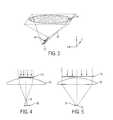
- FIG. 4is a cross-sectional view of a beam focusing lens in the BDS shown in FIG. 1 , illustrating the ‘y component’ of the highly compressed beam passing through the beam focusing lens.
- FIG. 5is a cross-sectional view of a beam focusing lens in the BDS shown in FIG. 1 , illustrating the ‘x component’ of the highly compressed beam passing through the beam focusing lens.
- FIG. 6is a cross-sectional view of the BDS shown in FIG. 1 , illustrating the formation of two separated focal points in one principal meridian.
- FIG. 7is a cross-sectional view of the BDS shown in FIG. 1 , illustrating the formation of two separated focal points in the other principal meridian.
- FIGS. 8 and 9are cross-sectional views of the BDS shown in FIG. 1 , illustrating the flexibility of adjusting processing parameters in the BDS.
- An adjustable astigmatic elongated beam spotmay be formed from a laser beam having ultrashort laser pulses and/or longer wavelengths, consistent with embodiments described herein, to machine substrates made of a variety of different materials.
- the laser beammay be generated with pulses having a pulse duration of less than 1 ns and/or having a wavelength greater than 400 nm.
- the laser beamis modified to produce an astigmatic beam that is collimated in a first axis and converging in a second axis.
- the astigmatic beamis focused to form the astigmatic elongated beam spot on a substrate, which is focused on the substrate in the first axis and defocused in the second axis.
- the astigmatic elongated beam spotmay be adjusted in length to provide an energy density sufficient for a single ultrashort pulse to cause cold ablation of at least a portion of the substrate material.
- the adjustable astigmatic elongated beam spotallows the energy density to be adjusted to avoid losing the benefit of using ultrashort pulses for ablation, as described in greater detail below.
- laser machiningand “laser processing” refer to any act of using laser energy to alter a workpiece and “scribing” refers to the act of machining or processing a workpiece by scanning the laser across the workpiece. Machining or processing may include, without limitation, ablation of the material at a surface of the workpiece and/or crystal damage of the material inside the workpiece. Scribing may include a series of ablations or crystal-damaged regions and does not require a continuous line of ablation or crystal damage.
- cold ablationrefers to the ablation or removal of material caused by absorption of laser energy while also removing heat through the ejection of ablated materials.
- Laser induced photonic ablationmay occur when atoms of a material with a defined bandgap are excited into higher quantum states through the absorption of energy.
- the energy of a single photonmeets or exceeds the bandgap of the target material (quantum absorption energy)
- laser energycan be absorbed, the exposed material is vaporized, and heat and debris are carried away in the plasma in a cold ablation process.
- the material bandgapexceeds the energy of a single photon (e.g., at longer wavelengths)
- multiphoton absorptionmay be required for cold ablation.
- Multiphoton absorptionis a non-linear intensity dependent process, and thus shorter pulses provide a more efficient process. Ultrashort laser pulses with high photonic energy, in particular, may provide an advantage in achieving multiphoton absorption.
- the benefits of using ultrashort laser pulses to achieve cold ablationmay be eliminated, however, when the energy density (J/cm 2 ) or the average power (W) used are too high above an optimum value. Because multiphoton absorption is not 100% efficient, a fraction of pulse energy may be converted to heat and remain in the material. Excess heat accumulation may result in melting and/or other heat damage. This heat may accumulate when excess energy is locally applied to the material, for example, by using an energy density above an optimum process and material dependent value. In one example, the energy density should be maintained below 5 J/cm 2 for a 10 ps pulse to avoid undesirable heat accumulation. This heat may also accumulate when ultrashort laser pulses are applied at higher repetition rates (e.g., at 100 kHz and greater).
- Higher repetition ratesmay also cause interaction of the laser pulse with the debris plume from a prior pulse, sometimes referred to as plasma shielding, which may cause material removal to be less effective.
- plasma shieldingmay also cause interaction of the laser pulse with the debris plume from a prior pulse, sometimes referred to as plasma shielding, which may cause material removal to be less effective.
- increased scanning speedsmay be one way to dissipate heat from high-repetition-rate lasers, accuracy may be sacrificed at higher scanning speeds.
- an astigmatic elongated beam spotmay improve laser processing speeds with lower repetition rates and lower part-movement speeds, thereby reducing localized heating because the energy is distributed over a larger area as well as overcoming the plasma-shielding problem.
- Adjusting the length of the astigmatic elongated beam spotallows optimal use of the energy density with the available power to provide minimal heat accumulation while spreading the available energy over a large area to achieve the desired throughput.
- using ultrashort laser pulsesfacilitates the multiphoton absorption needed for cold ablation with higher wavelengths and the variable astigmatic elongated beam spot enables higher processing speeds without losing the cold ablation benefits of the ultrashort pulses.
- the variable astigmatic elongated beam spotallows use of the full range of pulse energy available out of any laser (and particularly ultrashort pulses) because the size of the beam spot may be optimized to match the optimum process fluence.
- speed (mm/s)pulse spacing (mm/pulse) ⁇ pulse frequency (pulses/s)
- pulse spacingbeam length/total shots per location.
- Increasing the beam lengththus increases the number of shots per location for a given pulse spacing.
- the longer beamallows an increased overlap (i.e., to achieve a desired depth of cut), which allows for increased cutting speeds while maintaining optimum fluence.
- the astigmatic elongated beam spotallows for generating narrower kerfs than those created by simply focusing the beam to a standard circular spot using traditional optical methods. Because diffraction limited focusing depends on wavelength, the astigmatic elongated beam spot facilitates the ability to achieve narrower kerfs at the longer wavelengths.
- a beam delivery system (BDS) 10capable of generating a variable astigmatic elongated beam spot is described in detail.
- the variable astigmatic elongated beam spotmay be used to cut or machine a substrate made of various types of materials.
- the BDS 10improves the productivity of LED die separation by forming a highly-resolved adjustable astigmatic elongated beam spot, which maximizes scribing speed and minimizes consumption of scribing-related real estate on a wafer.
- the BDS 10can also be used in other scribing or cutting applications.
- a solid-state laser 12preferably diode pumped, generates a raw laser beam.
- the raw laser beammay be a pulsed laser beam with ultrashort pulses, i.e., a pulse duration less than 1 nanosecond (ns), providing a peak power that causes multiphoton absorption.
- the ultrashort pulse durationmay be in any possible laser pulse duration range less than 1 ns, such as a range less than 10 picosecond (ps), a range less than 1 ps, or a range less than 1 femtosecond (fs).
- the laser beammay also have any possible laser wavelength including, without limitation, a wavelength in the UV range of about 100 nm to 380 nm (e.g., a 157 nm laser, a 266 nm laser, a 315 nm, or a 355 nm laser), a wavelength in the visible range of about 380 nm to 750 nm (e.g., a 515 nm or 532 nm green laser), a wavelength in the near IR range of about 0.75 ⁇ m to 1.3 ⁇ m (e.g., a 1.01 ⁇ m laser, a 1.03 ⁇ m, or a 1.07 ⁇ m laser), a wavelength in the mid IR range of 1.3 ⁇ m to 5 ⁇ m, and a wavelength in the far IR range of over 5 ⁇ m.
- a wavelength in the UV rangeof about 100 nm to 380 nm
- a wavelength in the visible range of about 380 nm to 750 nm
- an ultrafast lasermay be capable of producing the raw laser beam at different wavelengths (e.g., about 0.35 ⁇ m, 0.5 ⁇ m, 1 ⁇ m, 1.3 ⁇ m, 1.5 ⁇ m, 2 ⁇ m or any increments therebetween) and at different ultrashort pulse durations (e.g., less than about 10 ps, 1 ps, 1 fs, or any increments therebetween).
- An example of an ultrafast laserincludes one of the TruMicro series 5000 picosecond lasers available from TRUMPF.
- the lasermay also provide a pulse energy in a range of about 1 ⁇ J to 1000 ⁇ J at repetition rates in a range of about 10 to 1000 kHz.
- the lasermay be a fiber laser such as the type available from IPG Photonics.
- the raw laser beamis usually in TEM 00 mode with Gaussian distribution and is enlarged by a beam-expanding telescope (BET) 14 .
- the exemplary embodiment of the BET 14is composed of the spherical plano-concave lens 16 and spherical plano-convex lens 18 .
- D cf sx +f sv
- D cis a collimation distance.
- Combinations of f sx and f svcan be used to satisfy designed values of the magnification M and the collimation distance D c .
- the expanded beamis reflected by the 100% mirror 20 a and then directed to the beam shaping iris 22 .
- the beam shaping iris 22symmetrically crops out the low intensity edges of the beam in a Gaussian profile, leaving a high intensity portion passing through the iris 22 .
- the beamis then directed to the center of a variable anamorphic lens system 24 .
- the exemplary variable anamorphic lens system 24is composed of a cylindrical plano-concave lens 26 and a cylindrical plano-convex lens 28 .
- the constituents of the variable anamorphic lens system 24preferably satisfy a condition,
- the incident beamis asymmetrically modified in one of the two principal meridians, which appears in the horizontal direction in FIG. 1 .
- f cv
- the degree of convergenceincreases in only one principal meridian of the collimated incident beam.
- One principal meridian of the incident beamloses its collimation and converges after the variable anamorphic lens system 24 ; however, the other principal meridian is not affected and keeps its beam collimation.
- variable anamorphic lens system 24the size of the beam after the variable anamorphic lens system 24 is changed in only one principal meridian by adjusting the distance between the two lenses in the anamorphic system 24 .
- the anamorphic BDS 10deliberately introduces astigmatism to produce focal points separated in two principal meridians, i.e. vertical and horizontal.
- the variable anamorphic lens systemcan be replaced by a single anamorphic lens for a fixed convergence.
- the exemplary beam focusing lens 30is an aberration corrected spherical multi-element lens having a focal length range between about +20 mm to +100 mm. In one embodiment of the BDS 10 , an edge-contact doublet with +50 mm focal length is used.
- a substrate 32such as a semiconductor wafer.
- the substrate 32is translated by computer controlled x-y motion stages 34 for scribing. In semiconductor scribing applications where the semiconductor wafer contains square or rectangular dies, the semiconductor wafer can be rotated 90 degrees by a rotary stage 36 for scribing in both the x direction and the y direction.
- the minimum beam waist diameter (w o ) or a size focused spotis inversely proportional to the incident beam diameter (w i ).
- the BET 14anamorphically increases the incident beam diameter (w i ) which is focused by the multi-element beam focusing lens 30 , resulting in a minimized beam waist diameter and yielding a highly-resolved focal beam spot.
- Thisprovides a sharply focused scribing beam spot capable of providing about 5 ⁇ m or less scribing kerf width on a semiconductor wafer. Consequently, the minimized scribing kerf width significantly reduces consumption of real estate on a wafer by scribing, which allows more dies on a wafer and improves productivity.
- variable anamorphic lens system 24results in two separate focal points in each principal meridian of the incident beam.
- the flexibility of changing beam convergence from the variable anamorphic lens system 24provides an instant modification of a laser energy density on a target semiconductor wafer. Since the optimum laser energy density is determined by light absorption properties of the particular target semiconductor wafer, the variable anamorphic lens system 24 can provide an instant adaptation to the optimum processing condition determined by various types of semiconductor wafers.
- anamorphic BDS 10can use different components to create the astigmatic focal beam spot or the anamorphic BDS 10 can include additional components to provide further modification of the beam.
- a bi-prism 38 or a set of bi-prismscan be inserted between the anamorphic lens system 24 and the BET 14 .
- the bi-prismequally divides the expanded and collimated beam from the BET 14 , then crosses the two divided beams over to produce an inversion of half Gaussian profile.
- the distance between the two divided beamscan be adjusted by changing the distance between the set of bi-prisms.
- the bi-prism 38divides the Gaussian beam by half circles and inverts the two divided half circles. A superimposition of these two circles creates superimposition of the edges of Gaussian profiles in weak intensity. This inversion of a Gaussian profile and intensity redistribution creates a homogeneous beam profile and eliminates certain drawbacks of a Gaussian intensity profile.
- the BDS 10can include an array of anamorphic lens systems 24 used to create small segments of separated astigmatic ‘beamlets’, similar to a dotted line.
- the astigmatic beamletsallow an effective escape of laser-induced plasma, which positively alters scribing results.
- the distance between the lenses in the array of anamorphic lens systemscontrols the length of each segment of the beamlets.
- the distance among the segments of the beamletscan be controlled by introducing a cylindrical plano-convex lens in front of the array of anamorphic lens systems.
- the BDS 10may include a high speed galvanometer followed by a focusing element such as an f-theta lens.
- the galvanometerallows the astigmatic elongated beam spot to be scanned across a workpiece or substrate in one or more axes without moving the workpiece.
- the f-theta lensallows the scanning beam from the galvanometer to be focused onto a flat surface of the substrate or workpiece without moving the lens. Other scan lenses may also be used.
- the profile of raw beam 50 from the lasergenerally has about 0.5 mm to 3 mm of diameter in a Gaussian distribution.
- the raw beam 50is expanded by the BET 14 and the expanded beam 52 is about 2.5 times larger in diameter.
- the expanded beam 52is passed through the beam shaping iris 22 for edge cropping and the expanded and edge-cropped beam 54 is directed to the center of the anamorphic lens system 24 .
- the anamorphic lens system 24modifies the expanded and edge-cropped beam 54 in only one principle meridian, resulting in a slightly compressed beam shape 56 .
- the highly compressed beam 57passes through the beam focusing lens 30 to form the astigmatic elongated beam spot 58 . Since the highly compressed beam 57 has converging beam characteristics in one principal meridian and collimated beam characteristics in the other, focal points are formed separately in each principal meridian after the beam focusing lens 30 .
- the three-dimensional diagram in FIG. 3illustrates in greater detail the formation of the two focal points separately in each principal meridian when the highly compressed beam 57 passes through the beam focusing lens (not shown). Since the highly compressed beam 57 in one principal meridian (hereinafter the ‘y component’) has converging characteristics, the y component exhibits the short distance focal point 60 . In contrast, since the other meridian (hereinafter the ‘x component’) has collimating beam characteristics, the x component exhibits the long distance focal point 62 . Combination of the x and y components results in the astigmatic beam spot 58 .
- FIG. 4shows the y component of the highly compressed beam 57 , which passes through the beam focusing lens 30 and results in the focal point 60 . After the focal point 60 , the beam diverges and creates the astigmatic side of the astigmatic elongated beam spot 58 .
- FIG. 5shows the x component of the highly compressed beam 57 , which passes through the beam focusing lens 30 and results in the focal point 62 .
- the collimated x component of the highly compressed beam 57is sharply focused at the focal point 60 , which creates the sharply focused side of the astigmatic elongated beam spot 58 .
- FIGS. 6 and 7illustrate further the formation of two separated focal points 60 , 62 in each principal meridian.
- the schematic beam tracings in FIGS. 6 and 7include two-dimensional layouts of the BDS 10 shown in FIG. 1 excluding the 100% mirrors 20 a , 20 b and the beam shaping iris 22 for simplicity.
- the raw beam from the solid-state laser 12is expanded by the BET 14 and then collimated.
- the variable anamorphic lens system 24modifies the collimated beam in this principle meridian, resulting in convergence of the beam.
- the converging beamis focused by the beam focusing lens 30 .
- the beamDue to its convergence from the variable anamorphic lens system 24 , the beam forms the focal point 60 , shorter than the nominal focal length of the beam focusing lens 30 .
- the beam tracing in FIG. 6is analogous to the view of the y component in FIG. 4 .
- the expanded and collimated beam from BET 14is not affected by the variable anamorphic lens system 24 in this principal meridian.
- the collimation of the beamcan be maintained in this meridian after the variable anamorphic lens system 24 .
- the collimated beamis focused at the focal point 62 , which is formed at a nominal focal length of the beam focusing lens 30 .
- the beam tracing in FIG. 7is analogous to the view of the x component in FIG. 5 . In FIG.
- the BET 14increases the incident beam diameter, which is focused by the multi-element beam focusing lens 30 , resulting in minimized a beam waist diameter and yielding a highly-resolved elongated beam spot.
- the target substrate 32e.g., a semiconductor wafer
- the combination of these two separated focal points 60 , 62generates an astigmatic elongated beam spot having one side with a defocused and compressed circumference and the other side with a sharply focused and short circumference.
- the astigmatic elongated beam spotis directed at the substrate and applied with a set of parameters (e.g., wavelength, energy density, pulse repetition rate, beam size) depending upon the material being scribed.
- the astigmatic elongated beam spotcan be used for scribing semiconductor wafers, for example, in wafer separation or dicing applications.
- the wafercan be moved or translated in at least one cutting direction under the focused laser beam to create one or more laser scribing cuts.
- a plurality of scribing cutscan be created by moving the wafer in an x direction and then by moving the wafer in a y direction after rotating the wafer 90 degrees.
- the astigmatic beam spotis generally insensitive to polarization factors because the wafer is rotated to provide the cuts in the x and y directions.
- the semiconductor wafercan be separated along the scribing cuts to form the dies using techniques known to those skilled in the art.
- the astigmatic elongated beam spotprovides an advantage in scribing applications by enabling faster scribing speeds.
- the pulse repetition rate r pdepends on the type of laser that is used. Solid state lasers with a few pulses per second to over 10 5 pulses per second are commercially available.
- the number of pulses n dis a material processing parameter, which is determined by material properties of the target wafer and a desired cut depth. Given the pulse repetition rate r p and the number of pulses n d , the beam length l b is a controlling factor to determine the speed of the cut.
- the focused astigmatic elongated beam spot formed according to the method described aboveincreases the beam length l b resulting in higher scribing speeds.
- variable anamorphic lens system 24also provides greater flexibility to adjust processing parameters for achieving an optimum condition.
- processing parametersshould preferably be adjusted for optimum conditions based on material properties of a target.
- the overflow of laser energy densitycan result in detrimental thermal damage to the target, and the lack of laser energy density can cause improper ablation or other undesired results.
- the energy density of an ultrashort pulse with higher irradiancemay need to be reduced to avoid losing the cold ablation benefits.
- the variable anamorphic lens system 24allows the energy density to be adjusted as needed depending on the pulse duration and other parameters such as laser power, wavelength, and material absorption properties.
- FIGS. 8 and 9show the flexibility of adjusting processing parameters of the BDS in this invention.
- the lenses 26 , 28 of the variable anamorphic lens system 24are placed close together, which results in low convergence of the collimated incident beam. This low convergence forms the focal point 60 at a relatively further distance from the beam focusing lens 30 . Consequently, the length of the beam spot 58 is relatively shorter and the energy density is increased.
- the lenses 26 , 28 of the variable anamorphic lens system 24are placed further apart, which results in high convergence of the collimated incident beam.
- This increased convergenceintroduces astigmatism and forms the focal point 60 at a relatively shorter distance from the beam focusing lens 30 . Consequently, the length of the beam spot 58 is relatively longer and the energy density is decreased.
- the astigmatic focal beam spotcan be used to scribe a sapphire substrate used for blue LEDs.
- Optimum processing of a sapphire substrate for blue LEDsgenerally requires an energy density of about 10 J/cm 2 .
- blue LED wafersare generally designed to have about a 50 ⁇ m gap among the individual die for separation, the optimum laser beam size is preferably less than about 20 ⁇ m for laser scribing.
- the conventional beam focusing at a 15 ⁇ m diameterresults in laser energy density of 34 J/cm 2 .
- the energy density on targethas to be adjusted by reducing the power output of the laser for optimum processing to avoid an overflow.
- the laser power outputcannot be fully utilized to maximize the scribing speed or productivity.
- the preferred embodiment of the BDS 10can adjust the size of the compressed beam spot to maintain the optimum laser energy density for 10 J/cm 2 without reducing the power output from the laser.
- the size of the astigmatic elongated beam spotcan be adjusted to have about 150 ⁇ m in the astigmatic axis and about 5 ⁇ m in the focused axis. Since the astigmatic axis is lined up in the scribing translation direction, this increase in beam length proportionally increases the scribing speed as discussed above. In this example, the astigmatic beam spot can provide processing speeds that are about 10 times faster than that of conventional beam focusing.
- the astigmatic focal beam spotcan be used to scribe a sapphire substrate by coupling with one or more GaN layers on the sapphire substrate (e.g., about 4 ⁇ 7 ⁇ m over the sapphire substrate) instead of coupling directly with sapphire.
- the lower bandgap of GaNprovides more efficient coupling with the incident laser beam, requiring only about 5 J/cm 2 for the laser energy density.
- the ablation through the sapphire substrateis much easier than direct coupling with the sapphire.
- the size of the astigmatic elongated beam spotcan be adjusted to have about 300 ⁇ m in the astigmatic axis and about 5 ⁇ m in the focused axis.
- the processing speedcan be 20 times faster than the conventional far field imaging or spot focusing techniques.
- a sapphire based LED wafermay be scribed with the astigmatic focal beam spot from the BDS 10 using a 266 nm DPSS laser with on target power of about 1.8 Watt at 50 kHz.
- the size of the astigmatic elongated beam spotmay be adjusted to have about 180 ⁇ m in the astigmatic axis and about 5 ⁇ m in the focused axis to provide a cut width of about 5 ⁇ m.
- the BDS 10is capable of scribing speeds of greater than 50 mm/sec.
- the laser cutforms a sharp V-shaped groove, which facilitates well controlled fracturing after the scribing.
- the variable astigmatic elongated beam spot from the adjustable BDS 10utilizes the maximum power output from the laser, which directly increases the processing speeds.
- front side scribingcan be used to decrease the street width and increase fracture yield, thereby increasing usable die per wafer.
- the astigmatic elongated beam spotcan also be used advantageously to scribe other types of semiconductor wafers.
- the astigmatic elongated beam spotreadily adjusts its laser energy density for an optimum value, based on the target material absorption properties, such as bandgap energy and surface roughness.
- a silicon wafermay be scribed with the astigmatic focal beam spot from the BDS 10 using a 266 nm DPSS laser with on target power of about 1.8 Watt at 50 kHz.
- the size of the astigmatic elongated beam spotmay be adjusted to have about 170 ⁇ m in the astigmatic axis and about 5 ⁇ m in the focused axis to produce 75 ⁇ m deep scribing with a speed at about 40 mm/sec.
- a GaP wafermay be scribed using a 266 nm DPSS laser with on target power of about 1.8 Watt at 50 kHz.
- the size of the astigmatic elongated beam spotmay be adjusted to have about 300 ⁇ m in the astigmatic axis and 5 ⁇ m in the focused axis to produce a 65 ⁇ m deep scribing with a speed at about 100 mm/sec. Similar results may be achieved in other compound semiconductor wafers such as GaAs, InP and Ge.
- Other semiconductor materialssuch as cadmium or bismuth telluride can also be scribed/machine with high speed high quality by using an astigmatic elongated beam spot and ultrashort pulses.
- a 532 nm 10 ps lasercan be used to form an astigmatic elongated beam spot 600 microns long by 20 microns wide to produce a 500 microns deep scribe with high speed (e.g., 2 meters/sec) multiple passes using 3 W average power at 200 kHz.
- the throughputcan be roughly doubled by adjusting the beam size using a 1200 microns long beam at 6 W and 200 Khz. If higher pulse energy is available, the throughput can further be increased by correspondingly increasing the beam length, while keeping an optimum fluence.
- substrates that can be scribedinclude, but are not limited to, InP, Alumina, glass, and polymers.
- the systems and methods described hereinmay also be used to scribe or process ceramic materials including, but not limited to, silicon nitride, silicon carbide, aluminum nitride, or ceramic phosphors used for light conversion in LEDs.
- the astigmatic focal beam spotcan also be used advantageously to scribe or machine metal films, such as molybdenum. Due to high thermal conductivity, laser cutting of metal films using conventional techniques has shown extensive heat affected zones along the wake of the laser cut. With the application of the astigmatic elongated beam spot, the 5 ⁇ m beam width in the focused axis significantly reduces a laser cutting kerf width, which subsequently reduces heat affected zones, collateral material damage and ablation-generated debris. The size of the astigmatic elongated beam spot was adjusted to have about 200 ⁇ m in the astigmatic axis and about 5 ⁇ m in the focused axis.
- the astigmatic elongated beam spotcan also be used to scribe other shapes or to perform other types of machining or cutting applications. Operating parameters other than those given in the above examples are also contemplated for scribing LED wafers.
- surface protectioncan be provided on the substrate by using a water soluble protective coating.
- the preferred composition of the protective coatingcomprises at least one surfactant in a water-soluble liquid glycerin and can be any kind of generic liquid detergent that satisfies this compositional requirement.
- the surfactant in the liquid glycerinforms a thin protective layer due to its high wetability. After the thin film layer is dried off, the glycerin effectively endures heat from the laser induced plasma, while preventing laser generated debris from adhering on the surface.
- the thin film of liquid detergentis easily removed by cleaning with pressurized water.
- the preferred embodiment of the present inventionprovides advantages over conventional systems using patterned laser projection and conventional systems using far field imaging. Unlike simple far field imaging, the present invention provides greater flexibility for modifying the laser beam by using the anamorphic BDS to produce the astigmatic elongated beam spot. Unlike conventional patterned laser projection, the anamorphic BDS delivers substantially the entire beam from a laser resonator to a target, thus maintaining very high beam utilization. The formation of the astigmatic elongated beam spot also allows the laser beam to have excellent characteristics in both the optimum intensity and the beam waist diameter. In particular, the preferred embodiment of the variable anamorphic lens system enables an adjustable uniplanar compression of a laser beam, which results in a variable focal beam spot for prompt adjustments of the optimum laser intensity.
- the formation of the astigmatic elongated beam spotresults in numerous advantages on separation of various semiconductor wafers, including fast scribing speeds, narrow scribing kerf width, reduced laser debris, and reduced collateral damage.
- the variable astigmatic elongated beam spotenables longer wavelength lasers with ultrashort pulses to be used for cold ablation with desired processing speeds and with minimal melting or heat damage.
- a methodfor forming an astigmatic elongated beam spot for machining a substrate.
- the methodincludes: generating a laser beam with pulses having a pulse duration of less than 1 ns; modifying the laser beam to produce an astigmatic beam that is collimated in a first axis and converging in a second axis; and focusing the astigmatic beam to form an astigmatic elongated beam spot on a substrate, the focused astigmatic beam having a first focal point in the first axis and a second focal point in the second axis, the second focal point being separate from the first focal point such that the astigmatic elongated beam spot is focused on the substrate in the first axis and defocused in the second axis, the astigmatic elongated beam spot having a width along the first axis and a length along the second axis, the width being less than the length such that the astigmatic elongated beam spot is narrower in the first axis and wider
- the methodincludes: generating a laser beam having a wavelength greater than 400 nm; modifying the laser beam to produce an astigmatic beam that is collimated in a first axis and converging in a second axis; and focusing the astigmatic beam to form an astigmatic elongated beam spot on a substrate, the focused astigmatic beam having a first focal point in the first axis and a second focal point in the second axis, the second focal point being separate from the first focal point such that the astigmatic elongated beam spot is focused on the substrate in the first axis and defocused in the second axis, the astigmatic elongated beam spot having a width along the first axis and a length along the second axis, the width being less than the length such that the astigmatic elongated beam spot is narrower in the first axis and wider in the second axis.
Landscapes
- Physics & Mathematics (AREA)
- Optics & Photonics (AREA)
- Engineering & Computer Science (AREA)
- Plasma & Fusion (AREA)
- Mechanical Engineering (AREA)
- Laser Beam Processing (AREA)
Abstract
Description
- This application is a continuation-in-part of co-pending U.S. patent application Ser. No. 13/422,190, filed Mar. 16, 2012, which is a continuation-in-part of U.S. patent application Ser. No. 12/962,050 filed Dec. 7, 2010, which claims the benefit of U.S. Provisional Patent Application Ser. No. 61/267,190 filed Dec. 7, 2009, both of which are incorporated herein by reference.
- This invention relates to laser processing, and more particularly, relates to laser processing, such as scribing, using an astigmatic elongated beam spot formed from a solid-state laser producing ultrashort pulses and/or longer wavelengths in the visible or IR ranges.
- Lasers are commonly used to process or machine a workpiece, for example, by cutting or scribing a substrate or semiconductor wafer. In semiconductor manufacturing, for example, a laser is often used in the process of dicing a semiconductor wafer such that individual devices (or dies) manufactured from the semiconductor wafer are separated from each other. The dies on the wafer are separated by streets and the laser may be used to cut the wafer along the streets. A laser may be used to cut all the way through the wafer, or part way through the wafer with the remaining portion of the wafer separated by breaking the wafer at the point of perforation. When manufacturing light emitting diodes (LEDs), for example, the individual dies on the wafer correspond to the LEDs.
- As the sizes of semiconductor devices decrease, the number of these devices that may be manufactured on a single wafer increases. Greater device density per wafer increases the yield and similarly reduces the cost of manufacturing per device. In order to increase this density, it is desirable to fabricate these devices as close together as possible. Positioning the devices more closely on the semiconductor wafer results in narrower streets between the devices. The laser beam is thus positioned precisely within the narrower streets and should scribe the wafer with minimal or no damage to the devices.
- According to one technique, a laser may be focused onto a surface of the substrate or wafer to cause ablation of the material and to effect a partial cut. Laser scribing may be performed on a semiconductor wafer, for example, on the front side of the wafer with the devices formed thereon, referred to as front-side scribing (FSS), or on the back side of the wafer, referred to as back-side scribing (BSS). Existing systems and methods have used an astigmatic elongated beam spot or line beam to perform laser scribing, for example, as described in greater detail in U.S. Pat. No. 7,709,768, which is incorporated herein by reference.
- Although such methods have provided advantages over other techniques for forming a line beam to scribe a workpiece, existing systems for scribing using an astigmatic elongated beam spot have been limited to certain materials, wavelengths, and pulse durations. Lasers producing ultrashort pulses and/or longer wavelengths in the visible and IR ranges have become commercially available but have presented challenges in certain laser scribing applications because of the desire to maintain high laser processing speeds and accuracy while minimizing melting and other heat damage.
- These and other features and advantages of the present invention will be better understood by reading the following detailed description, taken together with the drawings wherein:
FIG. 1 is a schematic diagram of a beam delivery system (BDS) with astigmatic focal point optics, according to one embodiment of the present invention.FIG. 2 is a schematic diagram of the BDS shown inFIG. 1 illustrating the sequential modification of the laser beam from the laser to the target.FIG. 3 is a cross-sectional view of a beam, illustrating the formation of two focal points separately in each principal meridian.FIG. 4 is a cross-sectional view of a beam focusing lens in the BDS shown inFIG. 1 , illustrating the ‘y component’ of the highly compressed beam passing through the beam focusing lens.FIG. 5 is a cross-sectional view of a beam focusing lens in the BDS shown inFIG. 1 , illustrating the ‘x component’ of the highly compressed beam passing through the beam focusing lens.FIG. 6 is a cross-sectional view of the BDS shown inFIG. 1 , illustrating the formation of two separated focal points in one principal meridian.FIG. 7 is a cross-sectional view of the BDS shown inFIG. 1 , illustrating the formation of two separated focal points in the other principal meridian.FIGS. 8 and 9 are cross-sectional views of the BDS shown inFIG. 1 , illustrating the flexibility of adjusting processing parameters in the BDS.- An adjustable astigmatic elongated beam spot may be formed from a laser beam having ultrashort laser pulses and/or longer wavelengths, consistent with embodiments described herein, to machine substrates made of a variety of different materials. The laser beam may be generated with pulses having a pulse duration of less than 1 ns and/or having a wavelength greater than 400 nm. The laser beam is modified to produce an astigmatic beam that is collimated in a first axis and converging in a second axis. The astigmatic beam is focused to form the astigmatic elongated beam spot on a substrate, which is focused on the substrate in the first axis and defocused in the second axis. The astigmatic elongated beam spot may be adjusted in length to provide an energy density sufficient for a single ultrashort pulse to cause cold ablation of at least a portion of the substrate material. Thus, the adjustable astigmatic elongated beam spot allows the energy density to be adjusted to avoid losing the benefit of using ultrashort pulses for ablation, as described in greater detail below.
- As used herein, “laser machining” and “laser processing” refer to any act of using laser energy to alter a workpiece and “scribing” refers to the act of machining or processing a workpiece by scanning the laser across the workpiece. Machining or processing may include, without limitation, ablation of the material at a surface of the workpiece and/or crystal damage of the material inside the workpiece. Scribing may include a series of ablations or crystal-damaged regions and does not require a continuous line of ablation or crystal damage. As used herein, “cold ablation” refers to the ablation or removal of material caused by absorption of laser energy while also removing heat through the ejection of ablated materials.
- Laser induced photonic ablation may occur when atoms of a material with a defined bandgap are excited into higher quantum states through the absorption of energy. When the energy of a single photon meets or exceeds the bandgap of the target material (quantum absorption energy), laser energy can be absorbed, the exposed material is vaporized, and heat and debris are carried away in the plasma in a cold ablation process. When the material bandgap exceeds the energy of a single photon (e.g., at longer wavelengths), multiphoton absorption may be required for cold ablation. Multiphoton absorption is a non-linear intensity dependent process, and thus shorter pulses provide a more efficient process. Ultrashort laser pulses with high photonic energy, in particular, may provide an advantage in achieving multiphoton absorption.
- The benefits of using ultrashort laser pulses to achieve cold ablation may be eliminated, however, when the energy density (J/cm2) or the average power (W) used are too high above an optimum value. Because multiphoton absorption is not 100% efficient, a fraction of pulse energy may be converted to heat and remain in the material. Excess heat accumulation may result in melting and/or other heat damage. This heat may accumulate when excess energy is locally applied to the material, for example, by using an energy density above an optimum process and material dependent value. In one example, the energy density should be maintained below 5 J/cm2for a 10 ps pulse to avoid undesirable heat accumulation. This heat may also accumulate when ultrashort laser pulses are applied at higher repetition rates (e.g., at 100 kHz and greater). Higher repetition rates may also cause interaction of the laser pulse with the debris plume from a prior pulse, sometimes referred to as plasma shielding, which may cause material removal to be less effective. Although increased scanning speeds may be one way to dissipate heat from high-repetition-rate lasers, accuracy may be sacrificed at higher scanning speeds.
- Using an astigmatic elongated beam spot, consistent with embodiments described herein, may improve laser processing speeds with lower repetition rates and lower part-movement speeds, thereby reducing localized heating because the energy is distributed over a larger area as well as overcoming the plasma-shielding problem. Adjusting the length of the astigmatic elongated beam spot, as described in greater detail below, allows optimal use of the energy density with the available power to provide minimal heat accumulation while spreading the available energy over a large area to achieve the desired throughput. Thus, using ultrashort laser pulses facilitates the multiphoton absorption needed for cold ablation with higher wavelengths and the variable astigmatic elongated beam spot enables higher processing speeds without losing the cold ablation benefits of the ultrashort pulses. The variable astigmatic elongated beam spot allows use of the full range of pulse energy available out of any laser (and particularly ultrashort pulses) because the size of the beam spot may be optimized to match the optimum process fluence.
- Increasing the length of the variable astigmatic elongated beam spot also leads to increases in linear machining speeds. The linear machining speed may be determined as follows: speed (mm/s)=pulse spacing (mm/pulse)×pulse frequency (pulses/s), where pulse spacing=beam length/total shots per location. Increasing the beam length thus increases the number of shots per location for a given pulse spacing. In other words, the longer beam allows an increased overlap (i.e., to achieve a desired depth of cut), which allows for increased cutting speeds while maintaining optimum fluence.
- In addition to controlling the energy density used on target by changing the beam length, the astigmatic elongated beam spot allows for generating narrower kerfs than those created by simply focusing the beam to a standard circular spot using traditional optical methods. Because diffraction limited focusing depends on wavelength, the astigmatic elongated beam spot facilitates the ability to achieve narrower kerfs at the longer wavelengths.
- Referring to
FIG. 1 , one embodiment of a beam delivery system (BDS)10 capable of generating a variable astigmatic elongated beam spot is described in detail. The variable astigmatic elongated beam spot may be used to cut or machine a substrate made of various types of materials. In one exemplary application, theBDS 10 improves the productivity of LED die separation by forming a highly-resolved adjustable astigmatic elongated beam spot, which maximizes scribing speed and minimizes consumption of scribing-related real estate on a wafer. TheBDS 10 can also be used in other scribing or cutting applications. - In the embodiment shown, a solid-
state laser 12, preferably diode pumped, generates a raw laser beam. The raw laser beam may be a pulsed laser beam with ultrashort pulses, i.e., a pulse duration less than 1 nanosecond (ns), providing a peak power that causes multiphoton absorption. The ultrashort pulse duration may be in any possible laser pulse duration range less than 1 ns, such as a range less than 10 picosecond (ps), a range less than 1 ps, or a range less than 1 femtosecond (fs). The laser beam may also have any possible laser wavelength including, without limitation, a wavelength in the UV range of about 100 nm to 380 nm (e.g., a 157 nm laser, a 266 nm laser, a 315 nm, or a 355 nm laser), a wavelength in the visible range of about 380 nm to 750 nm (e.g., a 515 nm or 532 nm green laser), a wavelength in the near IR range of about 0.75 μm to 1.3 μm (e.g., a 1.01 μm laser, a 1.03 μm, or a 1.07 μm laser), a wavelength in the mid IR range of 1.3 μm to 5 μm, and a wavelength in the far IR range of over 5 μm. - In some embodiments, an ultrafast laser may be capable of producing the raw laser beam at different wavelengths (e.g., about 0.35 μm, 0.5 μm, 1 μm, 1.3 μm, 1.5 μm, 2 μm or any increments therebetween) and at different ultrashort pulse durations (e.g., less than about 10 ps, 1 ps, 1 fs, or any increments therebetween). An example of an ultrafast laser includes one of the TruMicro series 5000 picosecond lasers available from TRUMPF. The laser may also provide a pulse energy in a range of about 1 μJ to 1000 μJ at repetition rates in a range of about 10 to 1000 kHz. In other embodiments, the laser may be a fiber laser such as the type available from IPG Photonics.
- The raw laser beam is usually in TEM00mode with Gaussian distribution and is enlarged by a beam-expanding telescope (BET)14. The exemplary embodiment of the
BET 14 is composed of the spherical plano-concave lens 16 and spherical plano-convex lens 18. Magnification of theBET 14 is determined by the focal lengths of each lens, generally described by M=(|fsx|/|fsv|), where M is magnification, fsxis a focal length of the spherical plano-convex lens 18 and fsvis a focal length of the spherical plano-concave lens 16. To effect collimated beam expansion, the distance between the spherical plano-concave lens 16 and the spherical plano-convex lens 18 is determined by a general equation, Dc=fsx+fsv, where Dcis a collimation distance. Combinations of fsxand fsvcan be used to satisfy designed values of the magnification M and the collimation distance Dc. The range of M can be about 2× to 20×, and is preferably 2.5× in theexemplary BDS 10. Based on this preferred magnification of 2.5×, a combination of fsx=250 mm and fsv=−100 mm with Dc=150 mm is preferably used in thisBDS 10. - In the illustrated embodiment, the expanded beam is reflected by the 100% mirror20aand then directed to the
beam shaping iris 22. Thebeam shaping iris 22 symmetrically crops out the low intensity edges of the beam in a Gaussian profile, leaving a high intensity portion passing through theiris 22. The beam is then directed to the center of a variableanamorphic lens system 24. - The exemplary variable
anamorphic lens system 24 is composed of a cylindrical plano-concave lens 26 and a cylindrical plano-convex lens 28. The constituents of the variableanamorphic lens system 24 preferably satisfy a condition, |fcx|=|fcv| where fcxis a focal length of the cylindrical plano-convex lens 28 and fcvis a focal length of the cylindrical plano-concave lens 26. In the variableanamorphic lens system 24, the incident beam is asymmetrically modified in one of the two principal meridians, which appears in the horizontal direction inFIG. 1 . In theanamorphic lens system 24, when D<Dc, where D is a distance between a cylindrical plano-concave lens 26 and a cylindrical plano-convex lens 28 and Dcis a collimation distance, a parallel incident beam is diverging after theanamorphic lens system 24. In contrast, when D>Dc, a parallel incident beam is converging after theanamorphic lens system 24. In the embodiment of theanamorphic lens system 24 shown inFIG. 1 , the collimation distance is Dc=fcx+fcv=0, because |fcx|=fcv| and fcxhas a positive value and fcva negative value and D≦Dc. Accordingly, when D>0, the collimated incident beam is converging after theanamorphic lens system 24. - The degree of convergence or combined focal length (fas) of the
anamorphic system 24 is governed by the distance D, and it is generally expressed by the two lens principle: fas=fcxfcv/(fcx+fcv−D). Namely, the larger the distance D, the shorter the focal length fas. When the distance D increases, the degree of convergence increases in only one principal meridian of the collimated incident beam. One principal meridian of the incident beam loses its collimation and converges after the variableanamorphic lens system 24; however, the other principal meridian is not affected and keeps its beam collimation. Consequently, the size of the beam after the variableanamorphic lens system 24 is changed in only one principal meridian by adjusting the distance between the two lenses in theanamorphic system 24. Thus, theanamorphic BDS 10 deliberately introduces astigmatism to produce focal points separated in two principal meridians, i.e. vertical and horizontal. Although a series of anamorphic lenses in different focal lengths or convergences is preferred to provide a variable astigmatic beam spot, the variable anamorphic lens system can be replaced by a single anamorphic lens for a fixed convergence. - After the variable
anamorphic lens system 24, the beam is reflected by another 100% mirror 20b, and then directed to the center of abeam focusing lens 30. The exemplarybeam focusing lens 30 is an aberration corrected spherical multi-element lens having a focal length range between about +20 mm to +100 mm. In one embodiment of theBDS 10, an edge-contact doublet with +50 mm focal length is used. After thebeam focusing lens 30, one of the astigmatic focal points is sharply focused on asubstrate 32, such as a semiconductor wafer. In one preferred embodiment, thesubstrate 32 is translated by computer controlled x-y motion stages34 for scribing. In semiconductor scribing applications where the semiconductor wafer contains square or rectangular dies, the semiconductor wafer can be rotated 90 degrees by arotary stage 36 for scribing in both the x direction and the y direction. - The preferred combination of the
BET 14 and the multi-elementbeam focusing lens 30 yields a highly-resolved and adjustable astigmatic focal beam spot with minimal aberration and a minimized beam waist diameter. In general, a minimum beam waist diameter (wo) of a Gaussian beam can be expressed by: wo=λf/πwiwhere λ is a wavelength of an incident laser beam, f is a focal length of a beam focusing lens, π is the circular constant, and wiis a diameter of the incident beam. In a givenbeam focusing lens 30, the minimum beam waist diameter (wo) or a size focused spot is inversely proportional to the incident beam diameter (wi). In the exemplary embodiment of the present invention, theBET 14 anamorphically increases the incident beam diameter (wi) which is focused by the multi-elementbeam focusing lens 30, resulting in a minimized beam waist diameter and yielding a highly-resolved focal beam spot. This provides a sharply focused scribing beam spot capable of providing about 5 μm or less scribing kerf width on a semiconductor wafer. Consequently, the minimized scribing kerf width significantly reduces consumption of real estate on a wafer by scribing, which allows more dies on a wafer and improves productivity. - The combination of the variable
anamorphic lens system 24 and the high resolutionbeam focusing lens 30 results in two separate focal points in each principal meridian of the incident beam. The flexibility of changing beam convergence from the variableanamorphic lens system 24 provides an instant modification of a laser energy density on a target semiconductor wafer. Since the optimum laser energy density is determined by light absorption properties of the particular target semiconductor wafer, the variableanamorphic lens system 24 can provide an instant adaptation to the optimum processing condition determined by various types of semiconductor wafers. - Although one exemplary embodiment of the
anamorphic BDS 10 is shown and described, other embodiments are contemplated and within the scope of the present invention. In particular, theanamorphic BDS 10 can use different components to create the astigmatic focal beam spot or theanamorphic BDS 10 can include additional components to provide further modification of the beam. - In one alternative embodiment, a bi-prism38 or a set of bi-prisms can be inserted between the
anamorphic lens system 24 and theBET 14. The bi-prism equally divides the expanded and collimated beam from theBET 14, then crosses the two divided beams over to produce an inversion of half Gaussian profile. When a set of bi-prisms is used, the distance between the two divided beams can be adjusted by changing the distance between the set of bi-prisms. In other words, the bi-prism38 divides the Gaussian beam by half circles and inverts the two divided half circles. A superimposition of these two circles creates superimposition of the edges of Gaussian profiles in weak intensity. This inversion of a Gaussian profile and intensity redistribution creates a homogeneous beam profile and eliminates certain drawbacks of a Gaussian intensity profile. - In another embodiment, the
BDS 10 can include an array ofanamorphic lens systems 24 used to create small segments of separated astigmatic ‘beamlets’, similar to a dotted line. The astigmatic beamlets allow an effective escape of laser-induced plasma, which positively alters scribing results. The distance between the lenses in the array of anamorphic lens systems controls the length of each segment of the beamlets. The distance among the segments of the beamlets can be controlled by introducing a cylindrical plano-convex lens in front of the array of anamorphic lens systems. - In other embodiments, the
BDS 10 may include a high speed galvanometer followed by a focusing element such as an f-theta lens. The galvanometer allows the astigmatic elongated beam spot to be scanned across a workpiece or substrate in one or more axes without moving the workpiece. The f-theta lens allows the scanning beam from the galvanometer to be focused onto a flat surface of the substrate or workpiece without moving the lens. Other scan lenses may also be used. - Referring to
FIG. 2 , one method of forming a variable astigmatic elongated beam spot is described in greater detail. The profile ofraw beam 50 from the laser generally has about 0.5 mm to 3 mm of diameter in a Gaussian distribution. Theraw beam 50 is expanded by theBET 14 and the expandedbeam 52 is about 2.5 times larger in diameter. The expandedbeam 52 is passed through thebeam shaping iris 22 for edge cropping and the expanded and edge-croppedbeam 54 is directed to the center of theanamorphic lens system 24. Theanamorphic lens system 24 modifies the expanded and edge-croppedbeam 54 in only one principle meridian, resulting in a slightly compressedbeam shape 56. As the slightly compressedlaser beam 56 travels towards thebeam focusing lens 30, the degree of astigmatism is increased in the beam shape since the variableanamorphic lens system 24 makes the beam converge in only one principal meridian. Subsequently, the highly compressed beam57 passes through thebeam focusing lens 30 to form the astigmatic elongatedbeam spot 58. Since the highly compressed beam57 has converging beam characteristics in one principal meridian and collimated beam characteristics in the other, focal points are formed separately in each principal meridian after thebeam focusing lens 30. Although this method of forming the astigmatic elongatedbeam spot 58 is described in the context of theexemplary BDS 10, this is not a limitation on the method. - The three-dimensional diagram in
FIG. 3 illustrates in greater detail the formation of the two focal points separately in each principal meridian when the highly compressed beam57 passes through the beam focusing lens (not shown). Since the highly compressed beam57 in one principal meridian (hereinafter the ‘y component’) has converging characteristics, the y component exhibits the short distancefocal point 60. In contrast, since the other meridian (hereinafter the ‘x component’) has collimating beam characteristics, the x component exhibits the long distancefocal point 62. Combination of the x and y components results in theastigmatic beam spot 58. FIG. 4 shows the y component of the highly compressed beam57, which passes through thebeam focusing lens 30 and results in thefocal point 60. After thefocal point 60, the beam diverges and creates the astigmatic side of the astigmatic elongatedbeam spot 58.FIG. 5 shows the x component of the highly compressed beam57, which passes through thebeam focusing lens 30 and results in thefocal point 62. The collimated x component of the highly compressed beam57 is sharply focused at thefocal point 60, which creates the sharply focused side of the astigmatic elongatedbeam spot 58.FIGS. 6 and 7 illustrate further the formation of two separatedfocal points FIGS. 6 and 7 include two-dimensional layouts of theBDS 10 shown inFIG. 1 excluding the 100% mirrors20a,20band thebeam shaping iris 22 for simplicity. InFIG. 6 , the raw beam from the solid-state laser 12 is expanded by theBET 14 and then collimated. The variableanamorphic lens system 24 modifies the collimated beam in this principle meridian, resulting in convergence of the beam. The converging beam is focused by thebeam focusing lens 30. Due to its convergence from the variableanamorphic lens system 24, the beam forms thefocal point 60, shorter than the nominal focal length of thebeam focusing lens 30. The beam tracing inFIG. 6 is analogous to the view of the y component inFIG. 4 .- In contrast, in
FIG. 7 , the expanded and collimated beam fromBET 14 is not affected by the variableanamorphic lens system 24 in this principal meridian. The collimation of the beam can be maintained in this meridian after the variableanamorphic lens system 24. After passing though thebeam focusing lens 30, the collimated beam is focused at thefocal point 62, which is formed at a nominal focal length of thebeam focusing lens 30. The beam tracing inFIG. 7 is analogous to the view of the x component inFIG. 5 . InFIG. 7 , theBET 14 increases the incident beam diameter, which is focused by the multi-elementbeam focusing lens 30, resulting in minimized a beam waist diameter and yielding a highly-resolved elongated beam spot. As a result, the target substrate32 (e.g., a semiconductor wafer) receives a wide and defocused astigmatic beam in one principal meridian and a narrow and sharply focused beam in the other principal meridian. - As illustrated in
FIG. 3 , the combination of these two separatedfocal points - To scribe a substrate, the astigmatic elongated beam spot is directed at the substrate and applied with a set of parameters (e.g., wavelength, energy density, pulse repetition rate, beam size) depending upon the material being scribed. According to one method, the astigmatic elongated beam spot can be used for scribing semiconductor wafers, for example, in wafer separation or dicing applications. In this method, the wafer can be moved or translated in at least one cutting direction under the focused laser beam to create one or more laser scribing cuts. To cut dies from a semiconductor wafer, a plurality of scribing cuts can be created by moving the wafer in an x direction and then by moving the wafer in a y direction after rotating the wafer90 degrees. When scribing in the x and y directions, the astigmatic beam spot is generally insensitive to polarization factors because the wafer is rotated to provide the cuts in the x and y directions. After the scribing cuts are made, the semiconductor wafer can be separated along the scribing cuts to form the dies using techniques known to those skilled in the art.
- The astigmatic elongated beam spot provides an advantage in scribing applications by enabling faster scribing speeds. The scribing speed can be denoted by S=(lb•rp)/nd, where S is the scribing speed (mm/sec), lbis the length of the focused scribing beam (mm), rpis pulse repetition rate (pulse/sec) and ndis the number of pulses required to achieve optimum scribing cut depth. The pulse repetition rate rpdepends on the type of laser that is used. Solid state lasers with a few pulses per second to over 105pulses per second are commercially available. The number of pulses ndis a material processing parameter, which is determined by material properties of the target wafer and a desired cut depth. Given the pulse repetition rate rpand the number of pulses nd, the beam length lbis a controlling factor to determine the speed of the cut. The focused astigmatic elongated beam spot formed according to the method described above increases the beam length lbresulting in higher scribing speeds.
- The variable
anamorphic lens system 24 also provides greater flexibility to adjust processing parameters for achieving an optimum condition. In laser material processing, for example, processing parameters should preferably be adjusted for optimum conditions based on material properties of a target. The overflow of laser energy density can result in detrimental thermal damage to the target, and the lack of laser energy density can cause improper ablation or other undesired results. In particular, the energy density of an ultrashort pulse with higher irradiance may need to be reduced to avoid losing the cold ablation benefits. As discussed in greater detail below, the variableanamorphic lens system 24 allows the energy density to be adjusted as needed depending on the pulse duration and other parameters such as laser power, wavelength, and material absorption properties. FIGS. 8 and 9 show the flexibility of adjusting processing parameters of the BDS in this invention. InFIG. 8 , thelenses anamorphic lens system 24 are placed close together, which results in low convergence of the collimated incident beam. This low convergence forms thefocal point 60 at a relatively further distance from thebeam focusing lens 30. Consequently, the length of thebeam spot 58 is relatively shorter and the energy density is increased.- In contrast, in
FIG. 9 , thelenses anamorphic lens system 24 are placed further apart, which results in high convergence of the collimated incident beam. This increased convergence introduces astigmatism and forms thefocal point 60 at a relatively shorter distance from thebeam focusing lens 30. Consequently, the length of thebeam spot 58 is relatively longer and the energy density is decreased. - In one scribing example, the astigmatic focal beam spot can be used to scribe a sapphire substrate used for blue LEDs. Optimum processing of a sapphire substrate for blue LEDs generally requires an energy density of about 10 J/cm2. Since blue LED wafers are generally designed to have about a 50 μm gap among the individual die for separation, the optimum laser beam size is preferably less than about 20 μm for laser scribing. When a currently-available commercial laser with 3 Watts on target output at 50 kHz pulse repetition is used, the conventional beam focusing at a 15 μm diameter results in laser energy density of 34 J/cm2. In a system with conventional beam spot focusing, the energy density on target has to be adjusted by reducing the power output of the laser for optimum processing to avoid an overflow. Thus, the laser power output cannot be fully utilized to maximize the scribing speed or productivity.
- In contrast, the preferred embodiment of the
BDS 10 can adjust the size of the compressed beam spot to maintain the optimum laser energy density for 10 J/cm2without reducing the power output from the laser. The size of the astigmatic elongated beam spot can be adjusted to have about 150 μm in the astigmatic axis and about 5 μm in the focused axis. Since the astigmatic axis is lined up in the scribing translation direction, this increase in beam length proportionally increases the scribing speed as discussed above. In this example, the astigmatic beam spot can provide processing speeds that are about 10 times faster than that of conventional beam focusing. - In another scribing example, the astigmatic focal beam spot can be used to scribe a sapphire substrate by coupling with one or more GaN layers on the sapphire substrate (e.g., about 4˜7 μm over the sapphire substrate) instead of coupling directly with sapphire. The lower bandgap of GaN provides more efficient coupling with the incident laser beam, requiring only about 5 J/cm2for the laser energy density. Once the laser beam couples with GaN, the ablation through the sapphire substrate is much easier than direct coupling with the sapphire. Accordingly, the size of the astigmatic elongated beam spot can be adjusted to have about 300 μm in the astigmatic axis and about 5 μm in the focused axis. Thus, the processing speed can be 20 times faster than the conventional far field imaging or spot focusing techniques.
- The minimized spot size in the focused axis also significantly reduces the scribing kerf width, which subsequently reduces consumption of a wafer real estate. Furthermore, by reducing total removed material volume, the narrow scribing cuts reduce collateral material damage and ablation-generated debris. In one example, a sapphire based LED wafer may be scribed with the astigmatic focal beam spot from the
BDS 10 using a 266 nm DPSS laser with on target power of about 1.8 Watt at 50 kHz. The size of the astigmatic elongated beam spot may be adjusted to have about 180 μm in the astigmatic axis and about 5 μm in the focused axis to provide a cut width of about 5 μm. Based on 30 μm deep scribing, theBDS 10 is capable of scribing speeds of greater than 50 mm/sec. The laser cut forms a sharp V-shaped groove, which facilitates well controlled fracturing after the scribing. The variable astigmatic elongated beam spot from theadjustable BDS 10 utilizes the maximum power output from the laser, which directly increases the processing speeds. Thus, front side scribing can be used to decrease the street width and increase fracture yield, thereby increasing usable die per wafer. - The astigmatic elongated beam spot can also be used advantageously to scribe other types of semiconductor wafers. The astigmatic elongated beam spot readily adjusts its laser energy density for an optimum value, based on the target material absorption properties, such as bandgap energy and surface roughness. In another example, a silicon wafer may be scribed with the astigmatic focal beam spot from the
BDS 10 using a 266 nm DPSS laser with on target power of about 1.8 Watt at 50 kHz. The size of the astigmatic elongated beam spot may be adjusted to have about 170 μm in the astigmatic axis and about 5 μm in the focused axis to produce 75 μm deep scribing with a speed at about 40 mm/sec. - In a further example, a GaP wafer may be scribed using a 266 nm DPSS laser with on target power of about 1.8 Watt at 50 kHz. The size of the astigmatic elongated beam spot may be adjusted to have about 300 μm in the astigmatic axis and 5 μm in the focused axis to produce a 65 μm deep scribing with a speed at about 100 mm/sec. Similar results may be achieved in other compound semiconductor wafers such as GaAs, InP and Ge.
- Other semiconductor materials such as cadmium or bismuth telluride can also be scribed/machine with high speed high quality by using an astigmatic elongated beam spot and ultrashort pulses. For example a 532
nm 10 ps laser can be used to form an astigmatic elongated beam spot 600 microns long by 20 microns wide to produce a 500 microns deep scribe with high speed (e.g., 2 meters/sec) multiple passes using 3 W average power at 200 kHz. In another example, the throughput can be roughly doubled by adjusting the beam size using a 1200 microns long beam at 6 W and 200 Khz. If higher pulse energy is available, the throughput can further be increased by correspondingly increasing the beam length, while keeping an optimum fluence. - Other substrates that can be scribed include, but are not limited to, InP, Alumina, glass, and polymers. The systems and methods described herein may also be used to scribe or process ceramic materials including, but not limited to, silicon nitride, silicon carbide, aluminum nitride, or ceramic phosphors used for light conversion in LEDs.
- The astigmatic focal beam spot can also be used advantageously to scribe or machine metal films, such as molybdenum. Due to high thermal conductivity, laser cutting of metal films using conventional techniques has shown extensive heat affected zones along the wake of the laser cut. With the application of the astigmatic elongated beam spot, the 5 μm beam width in the focused axis significantly reduces a laser cutting kerf width, which subsequently reduces heat affected zones, collateral material damage and ablation-generated debris. The size of the astigmatic elongated beam spot was adjusted to have about 200 μm in the astigmatic axis and about 5 μm in the focused axis. This resulted in 50 μm deep scribing with a speed at about 20 mm/sec, using 266 nm DPSS laser with on target power of about 2.5 Watt at 25 kHz. Other types of metal can also be cut including, but not limited to, aluminum, titanium or copper. These metals may having varying thicknesses, for example, including several hundreds of microns thick down to very thin films such as those used as metallization layers for contacts on solar cells.
- Although the examples show lines scribed in a substrate, the astigmatic elongated beam spot can also be used to scribe other shapes or to perform other types of machining or cutting applications. Operating parameters other than those given in the above examples are also contemplated for scribing LED wafers.
- According to another scribing method, surface protection can be provided on the substrate by using a water soluble protective coating. The preferred composition of the protective coating comprises at least one surfactant in a water-soluble liquid glycerin and can be any kind of generic liquid detergent that satisfies this compositional requirement. The surfactant in the liquid glycerin forms a thin protective layer due to its high wetability. After the thin film layer is dried off, the glycerin effectively endures heat from the laser induced plasma, while preventing laser generated debris from adhering on the surface. The thin film of liquid detergent is easily removed by cleaning with pressurized water.
- Accordingly, the preferred embodiment of the present invention provides advantages over conventional systems using patterned laser projection and conventional systems using far field imaging. Unlike simple far field imaging, the present invention provides greater flexibility for modifying the laser beam by using the anamorphic BDS to produce the astigmatic elongated beam spot. Unlike conventional patterned laser projection, the anamorphic BDS delivers substantially the entire beam from a laser resonator to a target, thus maintaining very high beam utilization. The formation of the astigmatic elongated beam spot also allows the laser beam to have excellent characteristics in both the optimum intensity and the beam waist diameter. In particular, the preferred embodiment of the variable anamorphic lens system enables an adjustable uniplanar compression of a laser beam, which results in a variable focal beam spot for prompt adjustments of the optimum laser intensity. By proper modification of beam spot and by maximized utilization of a raw beam, the formation of the astigmatic elongated beam spot results in numerous advantages on separation of various semiconductor wafers, including fast scribing speeds, narrow scribing kerf width, reduced laser debris, and reduced collateral damage. Moreover, the variable astigmatic elongated beam spot enables longer wavelength lasers with ultrashort pulses to be used for cold ablation with desired processing speeds and with minimal melting or heat damage.
- Consistent with an embodiment, a method is provided for forming an astigmatic elongated beam spot for machining a substrate. The method includes: generating a laser beam with pulses having a pulse duration of less than 1 ns; modifying the laser beam to produce an astigmatic beam that is collimated in a first axis and converging in a second axis; and focusing the astigmatic beam to form an astigmatic elongated beam spot on a substrate, the focused astigmatic beam having a first focal point in the first axis and a second focal point in the second axis, the second focal point being separate from the first focal point such that the astigmatic elongated beam spot is focused on the substrate in the first axis and defocused in the second axis, the astigmatic elongated beam spot having a width along the first axis and a length along the second axis, the width being less than the length such that the astigmatic elongated beam spot is narrower in the first axis and wider in the second axis.
- Consistent with another embodiment, the method includes: generating a laser beam having a wavelength greater than 400 nm; modifying the laser beam to produce an astigmatic beam that is collimated in a first axis and converging in a second axis; and focusing the astigmatic beam to form an astigmatic elongated beam spot on a substrate, the focused astigmatic beam having a first focal point in the first axis and a second focal point in the second axis, the second focal point being separate from the first focal point such that the astigmatic elongated beam spot is focused on the substrate in the first axis and defocused in the second axis, the astigmatic elongated beam spot having a width along the first axis and a length along the second axis, the width being less than the length such that the astigmatic elongated beam spot is narrower in the first axis and wider in the second axis.
- While the principles of the invention have been described herein, it is to be understood by those skilled in the art that this description is made only by way of example and not as a limitation as to the scope of the invention. Other embodiments are contemplated within the scope of the present invention in addition to the exemplary embodiments shown and described herein. Modifications and substitutions by one of ordinary skill in the art are considered to be within the scope of the present invention, which is not to be limited except by the following claims.
Claims (31)
1. A method of forming an astigmatic elongated beam spot for machining a substrate, the method comprising:
generating a laser beam with pulses having a pulse duration of less than 1 ns;
modifying the laser beam to produce an astigmatic beam that is collimated in a first axis and converging in a second axis; and
focusing the astigmatic beam to form an astigmatic elongated beam spot on a substrate, the focused astigmatic beam having a first focal point in the first axis and a second focal point in the second axis, the second focal point being separate from the first focal point such that the astigmatic elongated beam spot is focused on the substrate in the first axis and defocused in the second axis, the astigmatic elongated beam spot having a width along the first axis and a length along the second axis, the width being less than the length such that the astigmatic elongated beam spot is narrower in the first axis and wider in the second axis.
2. The method ofclaim 1 wherein the pulse duration is less than 10 ps.
3. The method ofclaim 1 wherein the pulse duration is less than 1 ps.
4. The method ofclaim 1 wherein the pulse duration is less than 1 fs.
5. The method ofclaim 1 wherein the laser beam has a wavelength greater than 400 nm.
6. The method ofclaim 1 wherein the laser beam has a wavelength in the IR range.
7. The method ofclaim 1 wherein the laser beam has a wavelength in the near IR range.
8. The method ofclaim 1 wherein the laser beam has a wavelength in the green visible range.
9. The method ofclaim 1 wherein the substrate includes a ceramic material.
10. The method ofclaim 1 wherein the substrate includes a metallic material.
11. The method of claiml wherein the substrate includes silicon.
12. The method ofclaim 1 wherein the substrate includes glass.
13. The method ofclaim 1 wherein an energy density of the astigmatic elongated beam spot is sufficient to cause cold ablation of at least a portion of the substrate with a single pulse of the laser.
14. The method ofclaim 13 further comprising causing the astigmatic elongated beam spot to move across the substrate in a direction of the second axis such that each successive pulse ablates at least a portion of the substrate, thereby scribing the substrate.
15. The method ofclaim 14 wherein causing the astigmatic elongated beam spot to move across the substrate includes moving the substrate in the direction of the second axis.
16. The method ofclaim 1 further comprising adjusting convergence of the laser beam in the second axis to adjust the length of the astigmatic elongated beam spot and an energy density of the astigmatic elongated beam spot on the substrate without adjusting the width of the of the astigmatic elongated beam spot.
17. The method ofclaim 16 wherein the energy density is adjusted such that a single pulse causes cold ablation of at least a portion of the substrate.
18. The method ofclaim 1 wherein modifying the laser beam includes passing the laser beam through an anamorphic lens system.
19. The method ofclaim 18 wherein the anamorphic lens system includes a cylindrical plano-concave lens and a cylindrical plano-convex lens.
20. The method ofclaim 19 further comprising:
adjusting the length of the astigmatic elongated beam spot and an energy density of the astigmatic elongated beam spot on the substrate without changing a width of the astigmatic elongated beam spot by adjusting a distance between the cylindrical plano-concave lens and the cylindrical plano-convex lens.
21. The method ofclaim 19 wherein the cylindrical plano-concave lens and the cylindrical plano-convex lens satisfy the condition |fcx|=|fcv|, where fcxis a focal length of the cylindrical plano-convex lens and has a positive value and where fcvis a focal length of the cylindrical plano-concave lens and has a negative value.
22. The method ofclaim 21 wherein a combined focal length (fas) of the anamorphic lens system changes with a distance (D) between the cylindrical plano-concave lens and the cylindrical plano-convex lens as follows: fas=fcx*fcv/(fcx+fcv−D).
23. The method ofclaim 1 wherein the laser beam is generated by a diode pumped solid-state (DPSS) laser.
24. The method of claiml wherein the laser beam is generated by a fiber laser.
25. The method ofclaim 1 further comprising expanding the laser beam and cropping edges of the expanded laser beam prior to modifying the laser beam.
26. A method of forming an astigmatic elongated beam spot for machining a substrate, the method comprising:
generating a laser beam having a wavelength greater than 400 nm;
modifying the laser beam to produce an astigmatic beam that is collimated in a first axis and converging in a second axis; and
focusing the astigmatic beam to form an astigmatic elongated beam spot on a substrate, the focused astigmatic beam having a first focal point in the first axis and a second focal point in the second axis, the second focal point being separate from the first focal point such that the astigmatic elongated beam spot is focused on the substrate in the first axis and defocused in the second axis, the astigmatic elongated beam spot having a width along the first axis and a length along the second axis, the width being less than the length such that the astigmatic elongated beam spot is narrower in the first axis and wider in the second axis.
27. The method ofclaim 26 wherein the laser beam has a wavelength in the IR range.
28. The method ofclaim 26 wherein the laser beam has a wavelength in the green visible range.
29. The method ofclaim 26 wherein the laser beam is generated with pulses having a pulse duration of less than 10 ps.
30. The method ofclaim 26 wherein focusing is performed with a fixed multi-element beam focusing lens.
31. The method ofclaim 26 wherein focusing is performed using a high speed galvanometer followed by a focusing element.
Priority Applications (3)
| Application Number | Priority Date | Filing Date | Title |
|---|---|---|---|
| US13/905,352US20130256286A1 (en) | 2009-12-07 | 2013-05-30 | Laser processing using an astigmatic elongated beam spot and using ultrashort pulses and/or longer wavelengths |
| PCT/US2014/040192WO2014194179A1 (en) | 2013-05-30 | 2014-05-30 | Laser processing using an astigmatic elongated beam spot and using ultrashort pulses and/or longer wavelengths |
| TW103118982ATW201446378A (en) | 2013-05-30 | 2014-05-30 | Laser processing using an astigmatic elongated beam spot and using ultrashort pulses and/or longer wavelengths |
Applications Claiming Priority (4)
| Application Number | Priority Date | Filing Date | Title |
|---|---|---|---|
| US26719009P | 2009-12-07 | 2009-12-07 | |
| US12/962,050US20110132885A1 (en) | 2009-12-07 | 2010-12-07 | Laser machining and scribing systems and methods |
| US13/422,190US20120234807A1 (en) | 2009-12-07 | 2012-03-16 | Laser scribing with extended depth affectation into a workplace |
| US13/905,352US20130256286A1 (en) | 2009-12-07 | 2013-05-30 | Laser processing using an astigmatic elongated beam spot and using ultrashort pulses and/or longer wavelengths |
Related Parent Applications (1)
| Application Number | Title | Priority Date | Filing Date |
|---|---|---|---|
| US13/422,190Continuation-In-PartUS20120234807A1 (en) | 2009-12-07 | 2012-03-16 | Laser scribing with extended depth affectation into a workplace |
Publications (1)
| Publication Number | Publication Date |
|---|---|
| US20130256286A1true US20130256286A1 (en) | 2013-10-03 |
Family
ID=49233487
Family Applications (1)
| Application Number | Title | Priority Date | Filing Date |
|---|---|---|---|
| US13/905,352AbandonedUS20130256286A1 (en) | 2009-12-07 | 2013-05-30 | Laser processing using an astigmatic elongated beam spot and using ultrashort pulses and/or longer wavelengths |
Country Status (1)
| Country | Link |
|---|---|
| US (1) | US20130256286A1 (en) |
Cited By (12)
| Publication number | Priority date | Publication date | Assignee | Title |
|---|---|---|---|---|
| US20120234807A1 (en)* | 2009-12-07 | 2012-09-20 | J.P. Sercel Associates Inc. | Laser scribing with extended depth affectation into a workplace |
| WO2015150014A1 (en)* | 2014-04-02 | 2015-10-08 | Arcam Ab | Method for fusing a workpiece |
| CN105108331A (en)* | 2015-07-28 | 2015-12-02 | 上海信耀电子有限公司 | Shaping light pipe and laser welding technology |
| WO2016193786A1 (en)* | 2015-06-01 | 2016-12-08 | Evana Technologies, Uab | Method of laser scribing of semiconductor workpiece using divided laser beams |
| DE102015010369A1 (en)* | 2015-08-13 | 2017-02-16 | Fraunhofer-Gesellschaft zur Förderung der angewandten Forschung e.V. | Method for removing brittle-hard material of a workpiece |
| WO2017216603A1 (en) | 2016-06-14 | 2017-12-21 | Evana Technologies, Uab | Laser processing method and a system for wafer dicing or cutting by use of a multi-segment focusing lens |
| US20190009362A1 (en)* | 2015-12-22 | 2019-01-10 | Heraeus Deutschland GmbH & Co. KG | Method for producing a metal-ceramic substrate with picolaser |
| US20190210156A1 (en)* | 2016-11-11 | 2019-07-11 | Beijing University Of Technology | Work fixture, device and method for machining the cutting edge of cutting tools |
| CN110091075A (en)* | 2019-05-31 | 2019-08-06 | 大族激光科技产业集团股份有限公司 | Wafer grooving method and device |
| US20200130103A1 (en)* | 2017-11-15 | 2020-04-30 | Advanced Technology Inc. | Laser patterning apparatus for 3-dimensional object and method |
| US11548094B2 (en) | 2017-02-15 | 2023-01-10 | General Electric Company | System and methods for fabricating a component with laser array |
| WO2023156982A1 (en)* | 2022-02-21 | 2023-08-24 | Innoviz Technologies Ltd. | Device for emitting a light beam and partial beam splitter |
Citations (196)
| Publication number | Priority date | Publication date | Assignee | Title |
|---|---|---|---|---|
| US3419321A (en)* | 1966-02-24 | 1968-12-31 | Lear Siegler Inc | Laser optical apparatus for cutting holes |
| US3544402A (en)* | 1967-06-02 | 1970-12-01 | Battelle Development Corp | Photographic reproduction by discrete intersecting rays with compression in the third dimension |
| US3626141A (en)* | 1970-04-30 | 1971-12-07 | Quantronix Corp | Laser scribing apparatus |
| US3629545A (en)* | 1967-12-19 | 1971-12-21 | Western Electric Co | Laser substrate parting |
| US3699644A (en)* | 1971-01-04 | 1972-10-24 | Sylvania Electric Prod | Method of dividing wafers |
| US3814895A (en)* | 1971-12-27 | 1974-06-04 | Electroglas Inc | Laser scriber control system |
| US3816700A (en)* | 1971-10-21 | 1974-06-11 | Union Carbide Corp | Apparatus for facilitating laser scribing |
| US3824678A (en)* | 1970-08-31 | 1974-07-23 | North American Rockwell | Process for laser scribing beam lead semiconductor wafers |
| US3967884A (en)* | 1974-11-05 | 1976-07-06 | Eastman Kodak Company | Three element objective lens |
| US3970819A (en)* | 1974-11-25 | 1976-07-20 | International Business Machines Corporation | Backside laser dicing system |
| US3983317A (en)* | 1974-12-09 | 1976-09-28 | Teletype Corporation | Astigmatizer for laser recording and reproducing system |
| US4043674A (en)* | 1974-10-02 | 1977-08-23 | Nasa | Spatial filter for Q-switched lasers |
| US4046985A (en)* | 1974-11-25 | 1977-09-06 | International Business Machines Corporation | Semiconductor wafer alignment apparatus |
| US4203651A (en)* | 1976-08-02 | 1980-05-20 | American Optical Corporation | Optical apparatus for varying focal power along one principal meridian while maintaining constant focal power along the other principal meridian |
| US4224101A (en)* | 1976-09-03 | 1980-09-23 | U.S. Philips Corporation | Method of manufacturing semiconductor devices using laser beam cutting |
| US4237601A (en)* | 1978-10-13 | 1980-12-09 | Exxon Research & Engineering Co. | Method of cleaving semiconductor diode laser wafers |
| US4253735A (en)* | 1978-04-28 | 1981-03-03 | Canon Kabushiki Kaisha | Image forming optical system for semiconductor laser |
| US4336439A (en)* | 1980-10-02 | 1982-06-22 | Coherent, Inc. | Method and apparatus for laser scribing and cutting |
| US4410237A (en)* | 1980-09-26 | 1983-10-18 | Massachusetts Institute Of Technology | Method and apparatus for shaping electromagnetic beams |
| US4433418A (en)* | 1981-02-06 | 1984-02-21 | Raytheon Company | Off-axis astigmatic unstable laser resonator |
| US4543464A (en)* | 1982-07-19 | 1985-09-24 | Tokyo Shibaura Denki Kabushiki Kaisha | Apparatus for scribing semiconductor wafer with laser beam |
| US4562333A (en)* | 1984-09-04 | 1985-12-31 | General Electric Company | Stress assisted cutting of high temperature embrittled materials |
| US4664739A (en)* | 1983-12-19 | 1987-05-12 | Stauffer Chemical Company | Removal of semiconductor wafers from dicing film |
| US4665913A (en)* | 1983-11-17 | 1987-05-19 | Lri L.P. | Method for ophthalmological surgery |
| US4718418A (en)* | 1983-11-17 | 1988-01-12 | Lri L.P. | Apparatus for ophthalmological surgery |
| US4729971A (en)* | 1987-03-31 | 1988-03-08 | Microwave Semiconductor Corporation | Semiconductor wafer dicing techniques |
| US4732148A (en)* | 1983-11-17 | 1988-03-22 | Lri L.P. | Method for performing ophthalmic laser surgery |
| US4752922A (en)* | 1984-07-06 | 1988-06-21 | Storage Technology Partners 11 | Optical disk recording and readout system having read, write and coarse light beams |
| US4851371A (en)* | 1988-12-05 | 1989-07-25 | Xerox Corporation | Fabricating process for large array semiconductive devices |
| US4865686A (en)* | 1986-09-26 | 1989-09-12 | Semiconductor Energy Laboratory Co., Ltd. | Laser scribing method |
| US4921564A (en)* | 1988-05-23 | 1990-05-01 | Semiconductor Equipment Corp. | Method and apparatus for removing circuit chips from wafer handling tape |
| US4964212A (en)* | 1988-09-29 | 1990-10-23 | Commissariat A L'energie Atomique | Process for producing electrical connections through a substrate |
| US4964704A (en)* | 1987-05-01 | 1990-10-23 | Semiconductor Energy Laboratory Co., Ltd. | Optical system for use of a laser processing machine |
| US4992393A (en)* | 1989-06-01 | 1991-02-12 | Ricoh Company, Ltd. | Method for producing semiconductor thin film by melt and recrystallization process |
| US5023426A (en)* | 1989-06-21 | 1991-06-11 | Honeywell Inc. | Robotic laser soldering apparatus for automated surface assembly of microscopic components |
| US5057664A (en)* | 1989-10-20 | 1991-10-15 | Electro Scientific Industries, Inc. | Method and apparatus for laser processing a target material to provide a uniformly smooth, continuous trim profile |
| US5075201A (en)* | 1990-10-31 | 1991-12-24 | Grumman Aerospace Corporation | Method for aligning high density infrared detector arrays |
| US5079772A (en)* | 1990-12-21 | 1992-01-07 | Coherent, Inc. | Mode-locked laser using non-linear self-focusing element |
| US5097471A (en)* | 1990-12-21 | 1992-03-17 | Coherent, Inc. | Mode-locked laser using non-linear self-focusing element |
| US5138131A (en)* | 1990-03-07 | 1992-08-11 | Matsushita Electric Industrial Co., Ltd. | Laser cutting method and apparatus for effecting said method |
| US5151389A (en)* | 1990-09-10 | 1992-09-29 | Rockwell International Corporation | Method for dicing semiconductor substrates using an excimer laser beam |
| US5163059A (en)* | 1991-05-09 | 1992-11-10 | Coherent, Inc. | Mode-locked laser using non-linear self-focusing element |
| US5181224A (en)* | 1991-05-10 | 1993-01-19 | University Of California | Microoptic lenses |
| US5185295A (en)* | 1990-05-16 | 1993-02-09 | Kabushiki Kaisha Toshiba | Method for dicing semiconductor substrates using a laser scribing and dual etch process |
| US5214261A (en)* | 1990-09-10 | 1993-05-25 | Rockwell International Corporation | Method and apparatus for dicing semiconductor substrates using an excimer laser beam |
| US5248877A (en)* | 1988-08-15 | 1993-09-28 | Anstalt Gersan | Making an elongate cut using high energy radiation |
| US5385633A (en)* | 1990-03-29 | 1995-01-31 | The United States Of America As Represented By The Secretary Of The Navy | Method for laser-assisted silicon etching using halocarbon ambients |
| US5387776A (en)* | 1993-05-11 | 1995-02-07 | General Electric Company | Method of separation of pieces from super hard material by partial laser cut and pressure cleavage |
| US5463200A (en)* | 1993-02-11 | 1995-10-31 | Lumonics Inc. | Marking of a workpiece by light energy |
| US5543365A (en)* | 1994-12-02 | 1996-08-06 | Texas Instruments Incorporated | Wafer scribe technique using laser by forming polysilicon |
| US5552345A (en)* | 1993-09-22 | 1996-09-03 | Harris Corporation | Die separation method for silicon on diamond circuit structures |
| US5611946A (en)* | 1994-02-18 | 1997-03-18 | New Wave Research | Multi-wavelength laser system, probe station and laser cutter system using the same |
| US5626777A (en)* | 1993-03-02 | 1997-05-06 | Hoechst Ceramtec Ag | Process for producing dividable plates of brittle material with high accuracy and apparatus for receiving and precision-grinding the end faces of a plate |
| US5627109A (en)* | 1994-09-16 | 1997-05-06 | Sassa; Michinari | Method of manufacturing a semiconductor device that uses a sapphire substrate |
| US5631190A (en)* | 1994-10-07 | 1997-05-20 | Cree Research, Inc. | Method for producing high efficiency light-emitting diodes and resulting diode structures |
| US5632083A (en)* | 1993-08-05 | 1997-05-27 | Hitachi Construction Machinery Co., Ltd. | Lead frame fabricating method and lead frame fabricating apparatus |
| US5634920A (en)* | 1992-10-01 | 1997-06-03 | Chiron Technolas Gmbh Ophthalmologische Systeme | Method and apparatus for removing epithelium from the surface of the eye |
| US5641416A (en)* | 1995-10-25 | 1997-06-24 | Micron Display Technology, Inc. | Method for particulate-free energy beam cutting of a wafer of die assemblies |
| US5675140A (en)* | 1995-02-10 | 1997-10-07 | Samsung Aerospace Industries, Ltd. | Autofocus control device with a light source |
| US5690845A (en)* | 1994-10-07 | 1997-11-25 | Sumitomo Electric Industries, Ltd. | Optical device for laser machining |
| US5759419A (en)* | 1995-10-05 | 1998-06-02 | Mitsubishi Chemical Corporation | Method of manufacturing a magnetic recording medium and a semiconductor laser texturing apparatus |
| US5796700A (en)* | 1996-06-15 | 1998-08-18 | Samsung Electronics Co., Ltd. | Optical pickup to circularize light emitted from a light source |
| US5801356A (en)* | 1995-08-16 | 1998-09-01 | Santa Barbara Research Center | Laser scribing on glass using Nd:YAG laser |
| US5809987A (en)* | 1996-11-26 | 1998-09-22 | Micron Technology,Inc. | Apparatus for reducing damage to wafer cutting blades during wafer dicing |
| US5837962A (en)* | 1996-07-15 | 1998-11-17 | Overbeck; James W. | Faster laser marker employing acousto-optic deflection |
| US5847746A (en)* | 1994-01-26 | 1998-12-08 | Canon Kabushiki Kaisha | Projection exposure apparatus including a condenser optical system for imaging a secondary light source at positions different in an optical axis direction with respect to two crossing planes |
| US5864171A (en)* | 1995-03-30 | 1999-01-26 | Kabushiki Kaisha Toshiba | Semiconductor optoelectric device and method of manufacturing the same |
| US5864430A (en)* | 1996-09-10 | 1999-01-26 | Sandia Corporation | Gaussian beam profile shaping apparatus, method therefor and evaluation thereof |
| US5872046A (en)* | 1996-04-10 | 1999-02-16 | Texas Instruments Incorporated | Method of cleaning wafer after partial saw |
| US5922224A (en)* | 1996-02-09 | 1999-07-13 | U.S. Philips Corporation | Laser separation of semiconductor elements formed in a wafer of semiconductor material |
| US5932118A (en)* | 1994-05-16 | 1999-08-03 | Sanyo Electric Co., Ltd. | Photoprocessing method |
| US5961852A (en)* | 1997-09-09 | 1999-10-05 | Optical Coating Laboratory, Inc. | Laser scribe and break process |
| US5976691A (en)* | 1996-12-19 | 1999-11-02 | Lintec Corporation | Process for producing chip and pressure sensitive adhesive sheet for said process |
| US5987920A (en)* | 1996-09-19 | 1999-11-23 | U.S. Philips Corporation | Method of producing a patterned surfacial marking on a transparent body |
| US5994205A (en)* | 1997-02-03 | 1999-11-30 | Kabushiki Kaisha Toshiba | Method of separating semiconductor devices |
| US6007218A (en)* | 1995-08-23 | 1999-12-28 | Science & Engineering Associates, Inc. | Self-contained laser illuminator module |
| US6057525A (en)* | 1995-09-05 | 2000-05-02 | United States Enrichment Corporation | Method and apparatus for precision laser micromachining |
| US6090100A (en)* | 1992-10-01 | 2000-07-18 | Chiron Technolas Gmbh Ophthalmologische Systeme | Excimer laser system for correction of vision with reduced thermal effects |
| US6107162A (en)* | 1995-12-19 | 2000-08-22 | Sony Corporation | Method for manufacture of cleaved light emitting semiconductor device |
| US6117347A (en)* | 1996-07-10 | 2000-09-12 | Nec Corporation | Method of separating wafers into individual die |
| US6121118A (en)* | 1998-11-30 | 2000-09-19 | Samsung Electronics Co., Ltd. | Chip separation device and method |
| US6130401A (en)* | 1998-07-29 | 2000-10-10 | Lg Electronics Inc. | Device and method for machining transparent medium by laser |
| US6133986A (en)* | 1996-02-28 | 2000-10-17 | Johnson; Kenneth C. | Microlens scanner for microlithography and wide-field confocal microscopy |
| US6140151A (en)* | 1998-05-22 | 2000-10-31 | Micron Technology, Inc. | Semiconductor wafer processing method |
| US6211488B1 (en)* | 1998-12-01 | 2001-04-03 | Accudyne Display And Semiconductor Systems, Inc. | Method and apparatus for separating non-metallic substrates utilizing a laser initiated scribe |
| US6219169B1 (en)* | 1999-01-07 | 2001-04-17 | Asahi Kogaku Kogyo Kabushiki Kaisha | Beam shape compensation optical system |
| US6266302B1 (en)* | 1998-03-12 | 2001-07-24 | Nec Corporation | Optical disk apparatus |
| US6273884B1 (en)* | 1997-05-15 | 2001-08-14 | Palomar Medical Technologies, Inc. | Method and apparatus for dermatology treatment |
| US6292584B1 (en)* | 1998-04-08 | 2001-09-18 | Lsp Technologies, Inc. | Image processing for laser peening |
| US6301059B1 (en)* | 2000-01-07 | 2001-10-09 | Lucent Technologies Inc. | Astigmatic compensation for an anamorphic optical system |
| US6309943B1 (en)* | 2000-04-25 | 2001-10-30 | Amkor Technology, Inc. | Precision marking and singulation method |
| US6341029B1 (en)* | 1999-04-27 | 2002-01-22 | Gsi Lumonics, Inc. | Method and apparatus for shaping a laser-beam intensity profile by dithering |
| US6341019B1 (en)* | 1997-06-12 | 2002-01-22 | Canon Kabushiki Kaisha | Method and apparatus for processing an image |
| US20020031899A1 (en)* | 1999-06-08 | 2002-03-14 | Ran Manor | Apparatus and method for singulating semiconductor wafers |
| USRE37585E1 (en)* | 1994-04-08 | 2002-03-19 | The Regents Of The University Of Michigan | Method for controlling configuration of laser induced breakdown and ablation |
| US6365429B1 (en)* | 1998-12-30 | 2002-04-02 | Xerox Corporation | Method for nitride based laser diode with growth substrate removed using an intermediate substrate |
| US6413839B1 (en)* | 1998-10-23 | 2002-07-02 | Emcore Corporation | Semiconductor device separation using a patterned laser projection |
| US20020088780A1 (en)* | 2000-10-26 | 2002-07-11 | Adrian Boyle | Control of laser machining |
| US6420776B1 (en)* | 2001-03-01 | 2002-07-16 | Amkor Technology, Inc. | Structure including electronic components singulated using laser cutting |
| US6433301B1 (en)* | 1999-05-28 | 2002-08-13 | Electro Scientific Industries, Inc. | Beam shaping and projection imaging with solid state UV Gaussian beam to form vias |
| US20020149136A1 (en)* | 2000-09-20 | 2002-10-17 | Baird Brian W. | Ultraviolet laser ablative patterning of microstructures in semiconductors |
| US6472295B1 (en)* | 1999-08-27 | 2002-10-29 | Jmar Research, Inc. | Method and apparatus for laser ablation of a target material |
| US20020162604A1 (en)* | 2001-03-09 | 2002-11-07 | Olivier Matile | Laser cutting method and apparatus with a bifocal optical means and a hydrogen-based assist gas |
| US20020170891A1 (en)* | 2001-03-22 | 2002-11-21 | Adrian Boyle | Laser machining system and method |
| US20020170898A1 (en)* | 2001-03-29 | 2002-11-21 | Ehrmann Jonathan S. | High-speed, precision, laser-based method and system for processing material of one or more targets within a field |
| US6509546B1 (en)* | 2000-03-15 | 2003-01-21 | International Business Machines Corporation | Laser excision of laminate chip carriers |
| US6511788B1 (en)* | 1999-02-12 | 2003-01-28 | Sony Corporation | Multi-layered optical disc |
| US6552301B2 (en)* | 2000-01-25 | 2003-04-22 | Peter R. Herman | Burst-ultrafast laser machining method |
| US6555447B2 (en)* | 1999-06-08 | 2003-04-29 | Kulicke & Soffa Investments, Inc. | Method for laser scribing of wafers |
| US20030102292A1 (en)* | 2001-12-01 | 2003-06-05 | Eo Technics Co., Ltd. | Method and apparatus for calibrating marking position in chip scale marker |
| US20030102291A1 (en)* | 2001-11-30 | 2003-06-05 | Xinbing Liu | System and method of laser drilling |
| US6580054B1 (en)* | 2002-06-10 | 2003-06-17 | New Wave Research | Scribing sapphire substrates with a solid state UV laser |
| US20030111447A1 (en)* | 2000-01-27 | 2003-06-19 | Corkum Paul B. | Method and apparatus for repair of defects in materials with short laser pulses |
| US20030142313A1 (en)* | 1998-07-03 | 2003-07-31 | Shoshi Katayama | Position detection apparatus and exposure apparatus |
| US6608852B2 (en)* | 2000-08-25 | 2003-08-19 | Lameda Physik Ag | Gain module for diode-pumped solid state laser and amplifier |
| US20030155333A1 (en)* | 2001-07-06 | 2003-08-21 | Kaidong Ye | Method and apparatus for cutting a substrate using laser irradiation |
| US20030160029A1 (en)* | 2002-01-30 | 2003-08-28 | Uht Corporation | Laser processing unit and processing apparatus comprising laser processing unit |
| US20030192866A1 (en)* | 2002-04-15 | 2003-10-16 | Eo Technics Co., Ltd. | Chip scale marker and making method |
| US6649494B2 (en)* | 2001-01-29 | 2003-11-18 | Matsushita Electric Industrial Co., Ltd. | Manufacturing method of compound semiconductor wafer |
| US20030217997A1 (en)* | 2001-04-30 | 2003-11-27 | Lsp Technologies, Inc. | Automated positioning of mobile laser peening head |
| US20030228739A1 (en)* | 2002-06-05 | 2003-12-11 | Nepomuceno Lamberto V. | Wafer cutting using laser marking |
| US6676878B2 (en)* | 2001-01-31 | 2004-01-13 | Electro Scientific Industries, Inc. | Laser segmented cutting |
| US20040031779A1 (en)* | 2002-05-17 | 2004-02-19 | Cahill Steven P. | Method and system for calibrating a laser processing system and laser marking system utilizing same |
| US20040112880A1 (en)* | 2002-12-13 | 2004-06-17 | Kazuma Sekiya | Laser machining method |
| US20040121493A1 (en)* | 2002-12-24 | 2004-06-24 | Eo Technics Co., Ltd. | Chip scale marker and method of calibrating marking position |
| US6765650B2 (en)* | 2001-08-09 | 2004-07-20 | Nikon Corporation | Vacuum compatible air bearing stage |
| US20040223133A1 (en)* | 2003-05-06 | 2004-11-11 | Canon Kabushiki Kaisha | Stage apparatus, exposure system using the same, and device manufacturing method |
| US20040228004A1 (en)* | 2003-02-19 | 2004-11-18 | Sercel Patrick J. | System and method for cutting using a variable astigmatic focal beam spot |
| US20040240491A1 (en)* | 2001-09-26 | 2004-12-02 | Achim Nebel | Device and method for converting an optical frequency |
| US20050006655A1 (en)* | 2001-11-09 | 2005-01-13 | Semiconductor Energy Laboratory Co., Ltd. | Laser beam treatment device and semiconductor device |
| US20050024743A1 (en)* | 2003-05-22 | 2005-02-03 | Frederic Camy-Peyret | Focusing optic for laser cutting |
| US20050042805A1 (en)* | 2003-07-11 | 2005-02-24 | Swenson Edward J. | Method of forming a scribe line on a passive electronic component substrate |
| US6881529B2 (en)* | 2001-05-14 | 2005-04-19 | Fuji Photo Film Co., Ltd. | Positive photoresist transfer material and method for processing surface of substrate using the transfer material |
| US20050185403A1 (en)* | 2004-02-20 | 2005-08-25 | Diehl Matthew D. | Laser dazzler matrix |
| US20050195474A1 (en)* | 2002-01-15 | 2005-09-08 | Jds Uniphase Corporation | Three -dimensional optical amplifier structure |
| US20050255716A1 (en)* | 2004-04-28 | 2005-11-17 | Semiconductor Energy Laboratory Co., Ltd. | Laser irradiation method and method for manufacturing semiconductor device using the same |
| US6992026B2 (en)* | 2000-09-13 | 2006-01-31 | Hamamatsu Photonics K.K. | Laser processing method and laser processing apparatus |
| US7005602B1 (en)* | 2004-02-27 | 2006-02-28 | Exatron, Inc. | Method and system for laser marking an article |
| US20060138098A1 (en)* | 1996-11-20 | 2006-06-29 | Ibiden Co., Ltd. | Laser machining apparatus, and apparatus and method for manufacturing a multilayered printed wiring board |
| US7079257B1 (en)* | 2002-04-08 | 2006-07-18 | Providence Health System | Methods and apparatus for evaluating mechanical and thermal strains in electronic materials, semiconductor materials, and other structures |
| US20060189034A1 (en)* | 2000-05-10 | 2006-08-24 | Nec Corporation | Thin film processing method and thin film processing apparatus |
| US7115903B2 (en)* | 2001-12-28 | 2006-10-03 | Semiconductor Energy Laboratory Co., Ltd. | Semiconductor device and semiconductor device producing system |
| US20060243711A1 (en)* | 2005-04-29 | 2006-11-02 | Robert Paradis | System and method for aligning a wafer processing system in a laser marking system |
| US20070051706A1 (en)* | 2005-09-08 | 2007-03-08 | Imra America, Inc. | Transparent material processing with an ultrashort pulse laser |
| US20070084838A1 (en)* | 2004-12-07 | 2007-04-19 | Chih-Ming Hsu | Method and cutting system for cutting a wafer by laser using a vacuum working table |
| US20070170159A1 (en)* | 2003-07-18 | 2007-07-26 | Hamamatsu Photonics K.K. | Laser beam machining method, laser beam machining apparatus, and laser beam machining product |
| US20070216892A1 (en)* | 2006-03-20 | 2007-09-20 | Boaz Eidelberg | Integrated large XY rotary positioning table with virtual center of rotation |
| US20070263693A1 (en)* | 2006-05-09 | 2007-11-15 | Spectralus Corporation | Compact efficient and robust ultraviolet |
| US20070272668A1 (en)* | 2006-05-25 | 2007-11-29 | Albelo Jeffrey A | Ultrashort laser pulse wafer scribing |
| US20070275541A1 (en)* | 2006-05-25 | 2007-11-29 | Harris Richard S | Back side wafer dicing |
| US20070298529A1 (en)* | 2006-05-31 | 2007-12-27 | Toyoda Gosei, Co., Ltd. | Semiconductor light-emitting device and method for separating semiconductor light-emitting devices |
| US20080014685A1 (en)* | 2006-07-17 | 2008-01-17 | Govorkov Sergei V | Amorphous silicon crystallization using combined beams from optically pumped semiconductor lasers |
| US20080090377A1 (en)* | 2003-02-10 | 2008-04-17 | Texas Instruments Incorporated | Laser scribe on front side of a semiconductor wafer |
| US20080225904A1 (en)* | 2005-11-01 | 2008-09-18 | Cymer, Inc. | Laser system |
| US20080267241A1 (en)* | 2005-11-01 | 2008-10-30 | Cymer, Inc. | Laser system |
| US20080296263A1 (en)* | 2002-02-25 | 2008-12-04 | Board Of Regents Of University Of Nebraska | Laser scribing and machining of materials |
| US20090007933A1 (en)* | 2007-03-22 | 2009-01-08 | Thomas James W | Methods for stripping and modifying surfaces with laser-induced ablation |
| US7486705B2 (en)* | 2004-03-31 | 2009-02-03 | Imra America, Inc. | Femtosecond laser processing system with process parameters, controls and feedback |
| US20090067468A1 (en)* | 2005-11-01 | 2009-03-12 | Cymer, Inc. | Laser system |
| US20090095721A1 (en)* | 2007-02-14 | 2009-04-16 | Scaggs Michael J | Precision laser machining apparatus |
| US20090122407A1 (en)* | 2005-08-16 | 2009-05-14 | Ohara Inc. | Structure and Manufacturing Method of the Same |
| US20090169871A1 (en)* | 2006-02-23 | 2009-07-02 | Reijo Lappalainen | Method for Producing High-Quality Surfaces and a Product Having a High-Quality Surface |
| US20090197393A1 (en)* | 2004-10-05 | 2009-08-06 | Hiroshi Haji | Method for dividing semiconductor wafer and manufacturing method for semiconductor devices |
| US20090201954A1 (en)* | 2007-08-01 | 2009-08-13 | Deep Photonics Corporation | Method and apparatus for pulsed harmonic ultraviolet lasers |
| US7576909B2 (en)* | 1998-07-16 | 2009-08-18 | Imra America, Inc. | Multimode amplifier for amplifying single mode light |
| US20090224432A1 (en)* | 2004-12-08 | 2009-09-10 | Syohei Nagatomo | Method of forming split originating point on object to be split, method of splitting object to be split, and method of processing object to be processed by pulse laser beam |
| US20090233811A1 (en)* | 2005-07-29 | 2009-09-17 | Randox Laboratories Ltd. | Manufacture of Array Chips |
| US20090261501A1 (en)* | 2008-04-18 | 2009-10-22 | Fujifilm Corporation | Manufacturing method for a stamper and manufacturing method for an optical information recording medium using the stamper |
| US20090296758A1 (en)* | 2005-11-01 | 2009-12-03 | Cymer, Inc. | Laser system |
| US20090296755A1 (en)* | 2005-11-01 | 2009-12-03 | Cymer, Inc. | Laser system |
| US20090294674A1 (en)* | 2005-04-06 | 2009-12-03 | Guillaume Bathelet | Method and Device for Eliminating Parasite Reflections During Inspection of Translucent or Transparent Hollow Objects |
| US20100015783A1 (en)* | 2002-03-12 | 2010-01-21 | Hamamatsu Photonics K.K. | Method of cutting an object to be processed |
| US20100012632A1 (en)* | 2006-09-19 | 2010-01-21 | Hamamatsu Photonics K.K. | Laser processing method |
| US7656578B2 (en)* | 1997-03-21 | 2010-02-02 | Imra America, Inc. | Microchip-Yb fiber hybrid optical amplifier for micro-machining and marking |
| US20100025387A1 (en)* | 2005-09-08 | 2010-02-04 | Imra America, Inc. | Transparent material processing with an ultrashort pulse laser |
| US20100119808A1 (en)* | 2008-11-10 | 2010-05-13 | Xinghua Li | Method of making subsurface marks in glass |
| US20100140630A1 (en)* | 2009-05-01 | 2010-06-10 | Bridgelux, Inc. | Method And Apparatus For Manufacturing LED Devices Using Laser Scribing |
| US20100197116A1 (en)* | 2008-03-21 | 2010-08-05 | Imra America, Inc. | Laser-based material processing methods and systems |
| US7829384B2 (en)* | 2007-09-25 | 2010-11-09 | Stats Chippac, Ltd. | Semiconductor device and method of laser-marking wafers with tape applied to its active surface |
| US20100301024A1 (en)* | 2009-05-28 | 2010-12-02 | Electro Scientific Industries, Inc. | Laser processing systems using through-the-lens alignment of a laser beam with a target feature |
| US20100324543A1 (en)* | 2007-09-18 | 2010-12-23 | Kurtz Ronald M | Method And Apparatus For Integrating Cataract Surgery With Glaucoma Or Astigmatism Surgery |
| US20110017716A1 (en)* | 2008-02-19 | 2011-01-27 | M-Solv Limited | Laser processing a multi-device panel |
| US7885309B2 (en)* | 2005-11-01 | 2011-02-08 | Cymer, Inc. | Laser system |
| US20110132885A1 (en)* | 2009-12-07 | 2011-06-09 | J.P. Sercel Associates, Inc. | Laser machining and scribing systems and methods |
| US7982228B2 (en)* | 2008-10-03 | 2011-07-19 | Versitech Limited | Semiconductor color-tunable broadband light sources and full-color microdisplays |
| US20110180696A1 (en)* | 2008-01-25 | 2011-07-28 | The Regents Of The University Of California | Devices useful for vacuum ultraviolet beam characterization |
| US20110193269A1 (en)* | 2008-09-01 | 2011-08-11 | Hamamatsu Photonics K.K. | Aberration-correcting method, laser processing method using said aberration-correcting method, laser irradiation method using said aberration-correcting method, aberration-correcting device and aberration-correcting program |
| US20110222391A1 (en)* | 2007-08-16 | 2011-09-15 | Fujifilm Corporation | Method for manufacturing medium on which information is recorded in pit pattern |
| US20110274128A1 (en)* | 2009-01-09 | 2011-11-10 | Hamamatsu Photonics K.K. | Laser beam working machine |
| US20120182850A1 (en)* | 2008-10-30 | 2012-07-19 | Sanyo Electric Co., Ltd. | Optical Pickup Apparatus and Disc Apparatus Including the Same |
| US20120234807A1 (en)* | 2009-12-07 | 2012-09-20 | J.P. Sercel Associates Inc. | Laser scribing with extended depth affectation into a workplace |
| US20120273472A1 (en)* | 2010-10-22 | 2012-11-01 | Electro Scientific Industries, Inc. | Laser processing systems and methods for beam dithering and skiving |
| US8399281B1 (en)* | 2011-08-31 | 2013-03-19 | Alta Devices, Inc. | Two beam backside laser dicing of semiconductor films |
| US20130121123A1 (en)* | 2010-07-13 | 2013-05-16 | Fujifilm Corporation | Method for recording on and reading out from optical information recording medium |
| US8537459B2 (en)* | 2004-03-31 | 2013-09-17 | Imra America, Inc. | Method and apparatus for controlling and protecting pulsed high power fiber amplifier systems |
| US8609512B2 (en)* | 2009-03-27 | 2013-12-17 | Electro Scientific Industries, Inc. | Method for laser singulation of chip scale packages on glass substrates |
- 2013
- 2013-05-30USUS13/905,352patent/US20130256286A1/ennot_activeAbandoned
Patent Citations (246)
| Publication number | Priority date | Publication date | Assignee | Title |
|---|---|---|---|---|
| US3419321A (en)* | 1966-02-24 | 1968-12-31 | Lear Siegler Inc | Laser optical apparatus for cutting holes |
| US3544402A (en)* | 1967-06-02 | 1970-12-01 | Battelle Development Corp | Photographic reproduction by discrete intersecting rays with compression in the third dimension |
| US3629545A (en)* | 1967-12-19 | 1971-12-21 | Western Electric Co | Laser substrate parting |
| US3626141A (en)* | 1970-04-30 | 1971-12-07 | Quantronix Corp | Laser scribing apparatus |
| US3824678A (en)* | 1970-08-31 | 1974-07-23 | North American Rockwell | Process for laser scribing beam lead semiconductor wafers |
| US3699644A (en)* | 1971-01-04 | 1972-10-24 | Sylvania Electric Prod | Method of dividing wafers |
| US3816700A (en)* | 1971-10-21 | 1974-06-11 | Union Carbide Corp | Apparatus for facilitating laser scribing |
| US3814895A (en)* | 1971-12-27 | 1974-06-04 | Electroglas Inc | Laser scriber control system |
| US4043674A (en)* | 1974-10-02 | 1977-08-23 | Nasa | Spatial filter for Q-switched lasers |
| US3967884A (en)* | 1974-11-05 | 1976-07-06 | Eastman Kodak Company | Three element objective lens |
| US3970819A (en)* | 1974-11-25 | 1976-07-20 | International Business Machines Corporation | Backside laser dicing system |
| US4046985A (en)* | 1974-11-25 | 1977-09-06 | International Business Machines Corporation | Semiconductor wafer alignment apparatus |
| US3983317A (en)* | 1974-12-09 | 1976-09-28 | Teletype Corporation | Astigmatizer for laser recording and reproducing system |
| US4203651A (en)* | 1976-08-02 | 1980-05-20 | American Optical Corporation | Optical apparatus for varying focal power along one principal meridian while maintaining constant focal power along the other principal meridian |
| US4224101A (en)* | 1976-09-03 | 1980-09-23 | U.S. Philips Corporation | Method of manufacturing semiconductor devices using laser beam cutting |
| US4253735A (en)* | 1978-04-28 | 1981-03-03 | Canon Kabushiki Kaisha | Image forming optical system for semiconductor laser |
| US4237601A (en)* | 1978-10-13 | 1980-12-09 | Exxon Research & Engineering Co. | Method of cleaving semiconductor diode laser wafers |
| US4410237A (en)* | 1980-09-26 | 1983-10-18 | Massachusetts Institute Of Technology | Method and apparatus for shaping electromagnetic beams |
| US4336439A (en)* | 1980-10-02 | 1982-06-22 | Coherent, Inc. | Method and apparatus for laser scribing and cutting |
| US4433418A (en)* | 1981-02-06 | 1984-02-21 | Raytheon Company | Off-axis astigmatic unstable laser resonator |
| US4543464A (en)* | 1982-07-19 | 1985-09-24 | Tokyo Shibaura Denki Kabushiki Kaisha | Apparatus for scribing semiconductor wafer with laser beam |
| US4665913A (en)* | 1983-11-17 | 1987-05-19 | Lri L.P. | Method for ophthalmological surgery |
| US4718418A (en)* | 1983-11-17 | 1988-01-12 | Lri L.P. | Apparatus for ophthalmological surgery |
| US4732148A (en)* | 1983-11-17 | 1988-03-22 | Lri L.P. | Method for performing ophthalmic laser surgery |
| US4664739A (en)* | 1983-12-19 | 1987-05-12 | Stauffer Chemical Company | Removal of semiconductor wafers from dicing film |
| US4752922A (en)* | 1984-07-06 | 1988-06-21 | Storage Technology Partners 11 | Optical disk recording and readout system having read, write and coarse light beams |
| US4562333A (en)* | 1984-09-04 | 1985-12-31 | General Electric Company | Stress assisted cutting of high temperature embrittled materials |
| USRE33947E (en)* | 1986-09-26 | 1992-06-02 | Semiconductor Energy Laboratory Co., Ltd. | Laser scribing method |
| US4865686A (en)* | 1986-09-26 | 1989-09-12 | Semiconductor Energy Laboratory Co., Ltd. | Laser scribing method |
| US4729971A (en)* | 1987-03-31 | 1988-03-08 | Microwave Semiconductor Corporation | Semiconductor wafer dicing techniques |
| US4964704A (en)* | 1987-05-01 | 1990-10-23 | Semiconductor Energy Laboratory Co., Ltd. | Optical system for use of a laser processing machine |
| US4921564A (en)* | 1988-05-23 | 1990-05-01 | Semiconductor Equipment Corp. | Method and apparatus for removing circuit chips from wafer handling tape |
| US5248877A (en)* | 1988-08-15 | 1993-09-28 | Anstalt Gersan | Making an elongate cut using high energy radiation |
| US4964212A (en)* | 1988-09-29 | 1990-10-23 | Commissariat A L'energie Atomique | Process for producing electrical connections through a substrate |
| US4851371A (en)* | 1988-12-05 | 1989-07-25 | Xerox Corporation | Fabricating process for large array semiconductive devices |
| US4992393A (en)* | 1989-06-01 | 1991-02-12 | Ricoh Company, Ltd. | Method for producing semiconductor thin film by melt and recrystallization process |
| US5023426A (en)* | 1989-06-21 | 1991-06-11 | Honeywell Inc. | Robotic laser soldering apparatus for automated surface assembly of microscopic components |
| US5057664A (en)* | 1989-10-20 | 1991-10-15 | Electro Scientific Industries, Inc. | Method and apparatus for laser processing a target material to provide a uniformly smooth, continuous trim profile |
| US5138131A (en)* | 1990-03-07 | 1992-08-11 | Matsushita Electric Industrial Co., Ltd. | Laser cutting method and apparatus for effecting said method |
| US5385633A (en)* | 1990-03-29 | 1995-01-31 | The United States Of America As Represented By The Secretary Of The Navy | Method for laser-assisted silicon etching using halocarbon ambients |
| US5185295A (en)* | 1990-05-16 | 1993-02-09 | Kabushiki Kaisha Toshiba | Method for dicing semiconductor substrates using a laser scribing and dual etch process |
| US5151389A (en)* | 1990-09-10 | 1992-09-29 | Rockwell International Corporation | Method for dicing semiconductor substrates using an excimer laser beam |
| US5214261A (en)* | 1990-09-10 | 1993-05-25 | Rockwell International Corporation | Method and apparatus for dicing semiconductor substrates using an excimer laser beam |
| US5075201A (en)* | 1990-10-31 | 1991-12-24 | Grumman Aerospace Corporation | Method for aligning high density infrared detector arrays |
| US5079772A (en)* | 1990-12-21 | 1992-01-07 | Coherent, Inc. | Mode-locked laser using non-linear self-focusing element |
| US5097471A (en)* | 1990-12-21 | 1992-03-17 | Coherent, Inc. | Mode-locked laser using non-linear self-focusing element |
| US5163059A (en)* | 1991-05-09 | 1992-11-10 | Coherent, Inc. | Mode-locked laser using non-linear self-focusing element |
| US5181224A (en)* | 1991-05-10 | 1993-01-19 | University Of California | Microoptic lenses |
| US6090100A (en)* | 1992-10-01 | 2000-07-18 | Chiron Technolas Gmbh Ophthalmologische Systeme | Excimer laser system for correction of vision with reduced thermal effects |
| US5634920A (en)* | 1992-10-01 | 1997-06-03 | Chiron Technolas Gmbh Ophthalmologische Systeme | Method and apparatus for removing epithelium from the surface of the eye |
| US5463200A (en)* | 1993-02-11 | 1995-10-31 | Lumonics Inc. | Marking of a workpiece by light energy |
| US5626777A (en)* | 1993-03-02 | 1997-05-06 | Hoechst Ceramtec Ag | Process for producing dividable plates of brittle material with high accuracy and apparatus for receiving and precision-grinding the end faces of a plate |
| US5387776A (en)* | 1993-05-11 | 1995-02-07 | General Electric Company | Method of separation of pieces from super hard material by partial laser cut and pressure cleavage |
| US5632083A (en)* | 1993-08-05 | 1997-05-27 | Hitachi Construction Machinery Co., Ltd. | Lead frame fabricating method and lead frame fabricating apparatus |
| US5552345A (en)* | 1993-09-22 | 1996-09-03 | Harris Corporation | Die separation method for silicon on diamond circuit structures |
| US5847746A (en)* | 1994-01-26 | 1998-12-08 | Canon Kabushiki Kaisha | Projection exposure apparatus including a condenser optical system for imaging a secondary light source at positions different in an optical axis direction with respect to two crossing planes |
| US5703713A (en)* | 1994-02-18 | 1997-12-30 | New Wave Research | Multi-wavelength variable attenuator and half wave plate |
| US5811751A (en)* | 1994-02-18 | 1998-09-22 | New Wave Research | Multi-wavelength laser system, probe station and laser cutter system using the same |
| US5963364A (en)* | 1994-02-18 | 1999-10-05 | New Wave Research | Multi-wavelength variable attenuator and half wave plate |
| US5611946A (en)* | 1994-02-18 | 1997-03-18 | New Wave Research | Multi-wavelength laser system, probe station and laser cutter system using the same |
| USRE37585E1 (en)* | 1994-04-08 | 2002-03-19 | The Regents Of The University Of Michigan | Method for controlling configuration of laser induced breakdown and ablation |
| US5932118A (en)* | 1994-05-16 | 1999-08-03 | Sanyo Electric Co., Ltd. | Photoprocessing method |
| US5627109A (en)* | 1994-09-16 | 1997-05-06 | Sassa; Michinari | Method of manufacturing a semiconductor device that uses a sapphire substrate |
| US5690845A (en)* | 1994-10-07 | 1997-11-25 | Sumitomo Electric Industries, Ltd. | Optical device for laser machining |
| US5631190A (en)* | 1994-10-07 | 1997-05-20 | Cree Research, Inc. | Method for producing high efficiency light-emitting diodes and resulting diode structures |
| US5912477A (en)* | 1994-10-07 | 1999-06-15 | Cree Research, Inc. | High efficiency light emitting diodes |
| US5543365A (en)* | 1994-12-02 | 1996-08-06 | Texas Instruments Incorporated | Wafer scribe technique using laser by forming polysilicon |
| US5675140A (en)* | 1995-02-10 | 1997-10-07 | Samsung Aerospace Industries, Ltd. | Autofocus control device with a light source |
| US5864171A (en)* | 1995-03-30 | 1999-01-26 | Kabushiki Kaisha Toshiba | Semiconductor optoelectric device and method of manufacturing the same |
| US5801356A (en)* | 1995-08-16 | 1998-09-01 | Santa Barbara Research Center | Laser scribing on glass using Nd:YAG laser |
| US6007218A (en)* | 1995-08-23 | 1999-12-28 | Science & Engineering Associates, Inc. | Self-contained laser illuminator module |
| US6057525A (en)* | 1995-09-05 | 2000-05-02 | United States Enrichment Corporation | Method and apparatus for precision laser micromachining |
| US5759419A (en)* | 1995-10-05 | 1998-06-02 | Mitsubishi Chemical Corporation | Method of manufacturing a magnetic recording medium and a semiconductor laser texturing apparatus |
| US5641416A (en)* | 1995-10-25 | 1997-06-24 | Micron Display Technology, Inc. | Method for particulate-free energy beam cutting of a wafer of die assemblies |
| US6107162A (en)* | 1995-12-19 | 2000-08-22 | Sony Corporation | Method for manufacture of cleaved light emitting semiconductor device |
| US5922224A (en)* | 1996-02-09 | 1999-07-13 | U.S. Philips Corporation | Laser separation of semiconductor elements formed in a wafer of semiconductor material |
| US6133986A (en)* | 1996-02-28 | 2000-10-17 | Johnson; Kenneth C. | Microlens scanner for microlithography and wide-field confocal microscopy |
| US5872046A (en)* | 1996-04-10 | 1999-02-16 | Texas Instruments Incorporated | Method of cleaning wafer after partial saw |
| US5796700A (en)* | 1996-06-15 | 1998-08-18 | Samsung Electronics Co., Ltd. | Optical pickup to circularize light emitted from a light source |
| US6117347A (en)* | 1996-07-10 | 2000-09-12 | Nec Corporation | Method of separating wafers into individual die |
| US5837962A (en)* | 1996-07-15 | 1998-11-17 | Overbeck; James W. | Faster laser marker employing acousto-optic deflection |
| US5864430A (en)* | 1996-09-10 | 1999-01-26 | Sandia Corporation | Gaussian beam profile shaping apparatus, method therefor and evaluation thereof |
| US5987920A (en)* | 1996-09-19 | 1999-11-23 | U.S. Philips Corporation | Method of producing a patterned surfacial marking on a transparent body |
| US20060138098A1 (en)* | 1996-11-20 | 2006-06-29 | Ibiden Co., Ltd. | Laser machining apparatus, and apparatus and method for manufacturing a multilayered printed wiring board |
| US5809987A (en)* | 1996-11-26 | 1998-09-22 | Micron Technology,Inc. | Apparatus for reducing damage to wafer cutting blades during wafer dicing |
| US5976691A (en)* | 1996-12-19 | 1999-11-02 | Lintec Corporation | Process for producing chip and pressure sensitive adhesive sheet for said process |
| US6225194B1 (en)* | 1996-12-19 | 2001-05-01 | Lintec Corporation | Process for producing chip and pressure sensitive adhesive sheet for said process |
| US5994205A (en)* | 1997-02-03 | 1999-11-30 | Kabushiki Kaisha Toshiba | Method of separating semiconductor devices |
| US7656578B2 (en)* | 1997-03-21 | 2010-02-02 | Imra America, Inc. | Microchip-Yb fiber hybrid optical amplifier for micro-machining and marking |
| US6273884B1 (en)* | 1997-05-15 | 2001-08-14 | Palomar Medical Technologies, Inc. | Method and apparatus for dermatology treatment |
| US6341019B1 (en)* | 1997-06-12 | 2002-01-22 | Canon Kabushiki Kaisha | Method and apparatus for processing an image |
| US5961852A (en)* | 1997-09-09 | 1999-10-05 | Optical Coating Laboratory, Inc. | Laser scribe and break process |
| US6266302B1 (en)* | 1998-03-12 | 2001-07-24 | Nec Corporation | Optical disk apparatus |
| US6292584B1 (en)* | 1998-04-08 | 2001-09-18 | Lsp Technologies, Inc. | Image processing for laser peening |
| US6683976B2 (en)* | 1998-04-08 | 2004-01-27 | Lsp Technologies, Inc. | Image processing for laser shock processing |
| US6140151A (en)* | 1998-05-22 | 2000-10-31 | Micron Technology, Inc. | Semiconductor wafer processing method |
| US20030142313A1 (en)* | 1998-07-03 | 2003-07-31 | Shoshi Katayama | Position detection apparatus and exposure apparatus |
| US7576909B2 (en)* | 1998-07-16 | 2009-08-18 | Imra America, Inc. | Multimode amplifier for amplifying single mode light |
| US6130401A (en)* | 1998-07-29 | 2000-10-10 | Lg Electronics Inc. | Device and method for machining transparent medium by laser |
| US6413839B1 (en)* | 1998-10-23 | 2002-07-02 | Emcore Corporation | Semiconductor device separation using a patterned laser projection |
| US6121118A (en)* | 1998-11-30 | 2000-09-19 | Samsung Electronics Co., Ltd. | Chip separation device and method |
| US6211488B1 (en)* | 1998-12-01 | 2001-04-03 | Accudyne Display And Semiconductor Systems, Inc. | Method and apparatus for separating non-metallic substrates utilizing a laser initiated scribe |
| US6365429B1 (en)* | 1998-12-30 | 2002-04-02 | Xerox Corporation | Method for nitride based laser diode with growth substrate removed using an intermediate substrate |
| US6219169B1 (en)* | 1999-01-07 | 2001-04-17 | Asahi Kogaku Kogyo Kabushiki Kaisha | Beam shape compensation optical system |
| US6511788B1 (en)* | 1999-02-12 | 2003-01-28 | Sony Corporation | Multi-layered optical disc |
| US20020041418A1 (en)* | 1999-04-27 | 2002-04-11 | Timothy Fillion | Method and apparatus for shaping a laser-beam intensity profile by dithering |
| US6341029B1 (en)* | 1999-04-27 | 2002-01-22 | Gsi Lumonics, Inc. | Method and apparatus for shaping a laser-beam intensity profile by dithering |
| US6433301B1 (en)* | 1999-05-28 | 2002-08-13 | Electro Scientific Industries, Inc. | Beam shaping and projection imaging with solid state UV Gaussian beam to form vias |
| US20020031899A1 (en)* | 1999-06-08 | 2002-03-14 | Ran Manor | Apparatus and method for singulating semiconductor wafers |
| US6555447B2 (en)* | 1999-06-08 | 2003-04-29 | Kulicke & Soffa Investments, Inc. | Method for laser scribing of wafers |
| US6472295B1 (en)* | 1999-08-27 | 2002-10-29 | Jmar Research, Inc. | Method and apparatus for laser ablation of a target material |
| US6301059B1 (en)* | 2000-01-07 | 2001-10-09 | Lucent Technologies Inc. | Astigmatic compensation for an anamorphic optical system |
| US6552301B2 (en)* | 2000-01-25 | 2003-04-22 | Peter R. Herman | Burst-ultrafast laser machining method |
| US20030111447A1 (en)* | 2000-01-27 | 2003-06-19 | Corkum Paul B. | Method and apparatus for repair of defects in materials with short laser pulses |
| US6509546B1 (en)* | 2000-03-15 | 2003-01-21 | International Business Machines Corporation | Laser excision of laminate chip carriers |
| US6309943B1 (en)* | 2000-04-25 | 2001-10-30 | Amkor Technology, Inc. | Precision marking and singulation method |
| US20060189034A1 (en)* | 2000-05-10 | 2006-08-24 | Nec Corporation | Thin film processing method and thin film processing apparatus |
| US6608852B2 (en)* | 2000-08-25 | 2003-08-19 | Lameda Physik Ag | Gain module for diode-pumped solid state laser and amplifier |
| US6992026B2 (en)* | 2000-09-13 | 2006-01-31 | Hamamatsu Photonics K.K. | Laser processing method and laser processing apparatus |
| US7825350B2 (en)* | 2000-09-13 | 2010-11-02 | Hamamatsu Photonics K.K. | Laser processing method and laser processing apparatus |
| US7396742B2 (en)* | 2000-09-13 | 2008-07-08 | Hamamatsu Photonics K.K. | Laser processing method for cutting a wafer-like object by using a laser to form modified regions within the object |
| US20020149136A1 (en)* | 2000-09-20 | 2002-10-17 | Baird Brian W. | Ultraviolet laser ablative patterning of microstructures in semiconductors |
| US6586707B2 (en)* | 2000-10-26 | 2003-07-01 | Xsil Technology Limited | Control of laser machining |
| US20020088780A1 (en)* | 2000-10-26 | 2002-07-11 | Adrian Boyle | Control of laser machining |
| US6649494B2 (en)* | 2001-01-29 | 2003-11-18 | Matsushita Electric Industrial Co., Ltd. | Manufacturing method of compound semiconductor wafer |
| US6676878B2 (en)* | 2001-01-31 | 2004-01-13 | Electro Scientific Industries, Inc. | Laser segmented cutting |
| US6420776B1 (en)* | 2001-03-01 | 2002-07-16 | Amkor Technology, Inc. | Structure including electronic components singulated using laser cutting |
| US20020162604A1 (en)* | 2001-03-09 | 2002-11-07 | Olivier Matile | Laser cutting method and apparatus with a bifocal optical means and a hydrogen-based assist gas |
| US20020170891A1 (en)* | 2001-03-22 | 2002-11-21 | Adrian Boyle | Laser machining system and method |
| US20070075058A1 (en)* | 2001-03-29 | 2007-04-05 | Gsi Lumonics Corporation | High-speed, precision, laser-based method and system for processing material of one or more targets within a field |
| US7148447B2 (en)* | 2001-03-29 | 2006-12-12 | Gsi Group Corporation | Method and apparatus for laser marking by ablation |
| US20050017156A1 (en)* | 2001-03-29 | 2005-01-27 | Gsi Lumonics Corporation | High-speed, precision, laser-based method and system for processing material of one or more targets within a field |
| US20020170898A1 (en)* | 2001-03-29 | 2002-11-21 | Ehrmann Jonathan S. | High-speed, precision, laser-based method and system for processing material of one or more targets within a field |
| US6777645B2 (en)* | 2001-03-29 | 2004-08-17 | Gsi Lumonics Corporation | High-speed, precision, laser-based method and system for processing material of one or more targets within a field |
| US20030217997A1 (en)* | 2001-04-30 | 2003-11-27 | Lsp Technologies, Inc. | Automated positioning of mobile laser peening head |
| US6867390B2 (en)* | 2001-04-30 | 2005-03-15 | Lsp Technologies, Inc | Automated positioning of mobile laser peening head |
| US6881529B2 (en)* | 2001-05-14 | 2005-04-19 | Fuji Photo Film Co., Ltd. | Positive photoresist transfer material and method for processing surface of substrate using the transfer material |
| US20030155333A1 (en)* | 2001-07-06 | 2003-08-21 | Kaidong Ye | Method and apparatus for cutting a substrate using laser irradiation |
| US6765650B2 (en)* | 2001-08-09 | 2004-07-20 | Nikon Corporation | Vacuum compatible air bearing stage |
| US20040240491A1 (en)* | 2001-09-26 | 2004-12-02 | Achim Nebel | Device and method for converting an optical frequency |
| US20050006655A1 (en)* | 2001-11-09 | 2005-01-13 | Semiconductor Energy Laboratory Co., Ltd. | Laser beam treatment device and semiconductor device |
| US20030102291A1 (en)* | 2001-11-30 | 2003-06-05 | Xinbing Liu | System and method of laser drilling |
| US6808117B2 (en)* | 2001-12-01 | 2004-10-26 | Eo Technics Co., Ltd. | Method and apparatus for calibrating marking position in chip scale marker |
| US20030102292A1 (en)* | 2001-12-01 | 2003-06-05 | Eo Technics Co., Ltd. | Method and apparatus for calibrating marking position in chip scale marker |
| US7652286B2 (en)* | 2001-12-28 | 2010-01-26 | Semiconductor Energy Laboratory Co., Ltd. | Semiconductor device and semiconductor device producing system |
| US7115903B2 (en)* | 2001-12-28 | 2006-10-03 | Semiconductor Energy Laboratory Co., Ltd. | Semiconductor device and semiconductor device producing system |
| US20070034877A1 (en)* | 2001-12-28 | 2007-02-15 | Semiconductor Energy Laboratory Co., Ltd. | Semiconductor device and semiconductor device producing system |
| US20050195474A1 (en)* | 2002-01-15 | 2005-09-08 | Jds Uniphase Corporation | Three -dimensional optical amplifier structure |
| US20030160029A1 (en)* | 2002-01-30 | 2003-08-28 | Uht Corporation | Laser processing unit and processing apparatus comprising laser processing unit |
| US20080296263A1 (en)* | 2002-02-25 | 2008-12-04 | Board Of Regents Of University Of Nebraska | Laser scribing and machining of materials |
| US7749867B2 (en)* | 2002-03-12 | 2010-07-06 | Hamamatsu Photonics K.K. | Method of cutting processed object |
| US20100015783A1 (en)* | 2002-03-12 | 2010-01-21 | Hamamatsu Photonics K.K. | Method of cutting an object to be processed |
| US7079257B1 (en)* | 2002-04-08 | 2006-07-18 | Providence Health System | Methods and apparatus for evaluating mechanical and thermal strains in electronic materials, semiconductor materials, and other structures |
| US6710286B2 (en)* | 2002-04-15 | 2004-03-23 | Eo Technics Co., Ltd. | Chip scale marker and making method |
| US20030192866A1 (en)* | 2002-04-15 | 2003-10-16 | Eo Technics Co., Ltd. | Chip scale marker and making method |
| US20040152233A1 (en)* | 2002-05-17 | 2004-08-05 | Chris Nemets | Method and system for machine vision-based feature detection and mark verification in a workpiece or wafer marking system |
| US20060186096A1 (en)* | 2002-05-17 | 2006-08-24 | Gsi Lumonics Corporation | High speed, laser-based marking method and system for producing machine readable marks on workpieces and semiconductor devices with reduced subsurface damage produced thereby |
| US20040031779A1 (en)* | 2002-05-17 | 2004-02-19 | Cahill Steven P. | Method and system for calibrating a laser processing system and laser marking system utilizing same |
| US20070031993A1 (en)* | 2002-05-17 | 2007-02-08 | Gsi Lumonics Corporation | Method and system for machine vision-based feature detection and mark verification in a workpiece or wafer marking system |
| US20030228739A1 (en)* | 2002-06-05 | 2003-12-11 | Nepomuceno Lamberto V. | Wafer cutting using laser marking |
| US6580054B1 (en)* | 2002-06-10 | 2003-06-17 | New Wave Research | Scribing sapphire substrates with a solid state UV laser |
| US20040112880A1 (en)* | 2002-12-13 | 2004-06-17 | Kazuma Sekiya | Laser machining method |
| US20040121493A1 (en)* | 2002-12-24 | 2004-06-24 | Eo Technics Co., Ltd. | Chip scale marker and method of calibrating marking position |
| US20080090377A1 (en)* | 2003-02-10 | 2008-04-17 | Texas Instruments Incorporated | Laser scribe on front side of a semiconductor wafer |
| US7388172B2 (en)* | 2003-02-19 | 2008-06-17 | J.P. Sercel Associates, Inc. | System and method for cutting using a variable astigmatic focal beam spot |
| US8502112B2 (en)* | 2003-02-19 | 2013-08-06 | Ipg Microsystems Llc | System and method for cutting using a variable astigmatic focal beam spot |
| US20080242056A1 (en)* | 2003-02-19 | 2008-10-02 | J.P. Sercel Associates, Inc. | System and method for cutting using a variable astigmatic focal beam spot |
| US20100301027A1 (en)* | 2003-02-19 | 2010-12-02 | J. P. Sercel Associates Inc. | System and method for cutting using a variable astigmatic focal beam spot |
| US20040228004A1 (en)* | 2003-02-19 | 2004-11-18 | Sercel Patrick J. | System and method for cutting using a variable astigmatic focal beam spot |
| US7709768B2 (en)* | 2003-02-19 | 2010-05-04 | Jp Sercel Associates Inc. | System and method for cutting using a variable astigmatic focal beam spot |
| US20040223133A1 (en)* | 2003-05-06 | 2004-11-11 | Canon Kabushiki Kaisha | Stage apparatus, exposure system using the same, and device manufacturing method |
| US20050024743A1 (en)* | 2003-05-22 | 2005-02-03 | Frederic Camy-Peyret | Focusing optic for laser cutting |
| US7241669B2 (en)* | 2003-07-11 | 2007-07-10 | Electro Scientific Industries, Inc. | Method of forming a scribe line on a passive electronic component substrate |
| US20050042805A1 (en)* | 2003-07-11 | 2005-02-24 | Swenson Edward J. | Method of forming a scribe line on a passive electronic component substrate |
| US20070170159A1 (en)* | 2003-07-18 | 2007-07-26 | Hamamatsu Photonics K.K. | Laser beam machining method, laser beam machining apparatus, and laser beam machining product |
| US20050185403A1 (en)* | 2004-02-20 | 2005-08-25 | Diehl Matthew D. | Laser dazzler matrix |
| US7005602B1 (en)* | 2004-02-27 | 2006-02-28 | Exatron, Inc. | Method and system for laser marking an article |
| US8537459B2 (en)* | 2004-03-31 | 2013-09-17 | Imra America, Inc. | Method and apparatus for controlling and protecting pulsed high power fiber amplifier systems |
| US20110139760A1 (en)* | 2004-03-31 | 2011-06-16 | Imra America, Inc. | Femtosecond laser processing system with process parameters controls and feedback |
| US7912100B2 (en)* | 2004-03-31 | 2011-03-22 | Imra America, Inc. | Femtosecond laser processing system with process parameters, controls and feedback |
| US7486705B2 (en)* | 2004-03-31 | 2009-02-03 | Imra America, Inc. | Femtosecond laser processing system with process parameters, controls and feedback |
| US20100304506A1 (en)* | 2004-04-28 | 2010-12-02 | Semiconductor Energy Laboratory Co., Ltd. | Laser irradiation method and method for manufacturing semiconductor device using the same |
| US7547866B2 (en)* | 2004-04-28 | 2009-06-16 | Semiconductor Energy Laboratory Co., Ltd. | Laser irradiation method and method for manufacturing semiconductor device including an autofocusing mechanism using the same |
| US7777210B2 (en)* | 2004-04-28 | 2010-08-17 | Semiconductor Energy Laboratory Co., Ltd. | Laser irradiation method in which a distance between an irradiation object and an optical system is controlled by an autofocusing mechanism and method for manufacturing semiconductor device using the same |
| US8022380B2 (en)* | 2004-04-28 | 2011-09-20 | Semiconductor Energy Laboratory Co., Ltd. | Laser irradiation method in which a distance between an irradiation object and an optical system is controlled by an autofocusing mechanism and method for manufacturing semiconductor device using the same |
| US20050255716A1 (en)* | 2004-04-28 | 2005-11-17 | Semiconductor Energy Laboratory Co., Ltd. | Laser irradiation method and method for manufacturing semiconductor device using the same |
| US20090250590A1 (en)* | 2004-04-28 | 2009-10-08 | Semiconductor Energy Laboratory Co., Ltd. | Laser irradiation method and method for manufacturing semiconductor device using the same |
| US20090197393A1 (en)* | 2004-10-05 | 2009-08-06 | Hiroshi Haji | Method for dividing semiconductor wafer and manufacturing method for semiconductor devices |
| US20070084838A1 (en)* | 2004-12-07 | 2007-04-19 | Chih-Ming Hsu | Method and cutting system for cutting a wafer by laser using a vacuum working table |
| US20090224432A1 (en)* | 2004-12-08 | 2009-09-10 | Syohei Nagatomo | Method of forming split originating point on object to be split, method of splitting object to be split, and method of processing object to be processed by pulse laser beam |
| US20090294674A1 (en)* | 2005-04-06 | 2009-12-03 | Guillaume Bathelet | Method and Device for Eliminating Parasite Reflections During Inspection of Translucent or Transparent Hollow Objects |
| US20060243711A1 (en)* | 2005-04-29 | 2006-11-02 | Robert Paradis | System and method for aligning a wafer processing system in a laser marking system |
| US20090233811A1 (en)* | 2005-07-29 | 2009-09-17 | Randox Laboratories Ltd. | Manufacture of Array Chips |
| US20090122407A1 (en)* | 2005-08-16 | 2009-05-14 | Ohara Inc. | Structure and Manufacturing Method of the Same |
| US20100025387A1 (en)* | 2005-09-08 | 2010-02-04 | Imra America, Inc. | Transparent material processing with an ultrashort pulse laser |
| US20070051706A1 (en)* | 2005-09-08 | 2007-03-08 | Imra America, Inc. | Transparent material processing with an ultrashort pulse laser |
| US20160067822A1 (en)* | 2005-09-08 | 2016-03-10 | Imra America, Inc. | Transparent material processing with an ultrashort pulse laser |
| US20100086741A1 (en)* | 2005-09-08 | 2010-04-08 | Imra America, Inc. | Transparent material processing with an ultrashort pulse laser |
| US7626138B2 (en)* | 2005-09-08 | 2009-12-01 | Imra America, Inc. | Transparent material processing with an ultrashort pulse laser |
| US20100084384A1 (en)* | 2005-09-08 | 2010-04-08 | Imra America, Inc. | Transparent material processing with an ultrashort pulse laser |
| US9138913B2 (en)* | 2005-09-08 | 2015-09-22 | Imra America, Inc. | Transparent material processing with an ultrashort pulse laser |
| US8144740B1 (en)* | 2005-11-01 | 2012-03-27 | Cymer, Inc. | Laser system |
| US20080225904A1 (en)* | 2005-11-01 | 2008-09-18 | Cymer, Inc. | Laser system |
| US20080267241A1 (en)* | 2005-11-01 | 2008-10-30 | Cymer, Inc. | Laser system |
| US20090296755A1 (en)* | 2005-11-01 | 2009-12-03 | Cymer, Inc. | Laser system |
| US20090296758A1 (en)* | 2005-11-01 | 2009-12-03 | Cymer, Inc. | Laser system |
| US7885309B2 (en)* | 2005-11-01 | 2011-02-08 | Cymer, Inc. | Laser system |
| US20090067468A1 (en)* | 2005-11-01 | 2009-03-12 | Cymer, Inc. | Laser system |
| US20090169871A1 (en)* | 2006-02-23 | 2009-07-02 | Reijo Lappalainen | Method for Producing High-Quality Surfaces and a Product Having a High-Quality Surface |
| US20070216892A1 (en)* | 2006-03-20 | 2007-09-20 | Boaz Eidelberg | Integrated large XY rotary positioning table with virtual center of rotation |
| US20070263693A1 (en)* | 2006-05-09 | 2007-11-15 | Spectralus Corporation | Compact efficient and robust ultraviolet |
| US20070272668A1 (en)* | 2006-05-25 | 2007-11-29 | Albelo Jeffrey A | Ultrashort laser pulse wafer scribing |
| US20070275541A1 (en)* | 2006-05-25 | 2007-11-29 | Harris Richard S | Back side wafer dicing |
| US20070298529A1 (en)* | 2006-05-31 | 2007-12-27 | Toyoda Gosei, Co., Ltd. | Semiconductor light-emitting device and method for separating semiconductor light-emitting devices |
| US7615722B2 (en)* | 2006-07-17 | 2009-11-10 | Coherent, Inc. | Amorphous silicon crystallization using combined beams from optically pumped semiconductor lasers |
| US20080014685A1 (en)* | 2006-07-17 | 2008-01-17 | Govorkov Sergei V | Amorphous silicon crystallization using combined beams from optically pumped semiconductor lasers |
| US20100012632A1 (en)* | 2006-09-19 | 2010-01-21 | Hamamatsu Photonics K.K. | Laser processing method |
| US20090095721A1 (en)* | 2007-02-14 | 2009-04-16 | Scaggs Michael J | Precision laser machining apparatus |
| US20090007933A1 (en)* | 2007-03-22 | 2009-01-08 | Thomas James W | Methods for stripping and modifying surfaces with laser-induced ablation |
| US20090201954A1 (en)* | 2007-08-01 | 2009-08-13 | Deep Photonics Corporation | Method and apparatus for pulsed harmonic ultraviolet lasers |
| US8323762B2 (en)* | 2007-08-16 | 2012-12-04 | Fujifilm Corporation | Method for manufacturing medium on which information is recorded in pit pattern |
| US20110222391A1 (en)* | 2007-08-16 | 2011-09-15 | Fujifilm Corporation | Method for manufacturing medium on which information is recorded in pit pattern |
| US20100324543A1 (en)* | 2007-09-18 | 2010-12-23 | Kurtz Ronald M | Method And Apparatus For Integrating Cataract Surgery With Glaucoma Or Astigmatism Surgery |
| US7829384B2 (en)* | 2007-09-25 | 2010-11-09 | Stats Chippac, Ltd. | Semiconductor device and method of laser-marking wafers with tape applied to its active surface |
| US20110180696A1 (en)* | 2008-01-25 | 2011-07-28 | The Regents Of The University Of California | Devices useful for vacuum ultraviolet beam characterization |
| US20110017716A1 (en)* | 2008-02-19 | 2011-01-27 | M-Solv Limited | Laser processing a multi-device panel |
| US20100197116A1 (en)* | 2008-03-21 | 2010-08-05 | Imra America, Inc. | Laser-based material processing methods and systems |
| US20090261501A1 (en)* | 2008-04-18 | 2009-10-22 | Fujifilm Corporation | Manufacturing method for a stamper and manufacturing method for an optical information recording medium using the stamper |
| US20110193269A1 (en)* | 2008-09-01 | 2011-08-11 | Hamamatsu Photonics K.K. | Aberration-correcting method, laser processing method using said aberration-correcting method, laser irradiation method using said aberration-correcting method, aberration-correcting device and aberration-correcting program |
| US7982228B2 (en)* | 2008-10-03 | 2011-07-19 | Versitech Limited | Semiconductor color-tunable broadband light sources and full-color microdisplays |
| US20120182850A1 (en)* | 2008-10-30 | 2012-07-19 | Sanyo Electric Co., Ltd. | Optical Pickup Apparatus and Disc Apparatus Including the Same |
| US20100119808A1 (en)* | 2008-11-10 | 2010-05-13 | Xinghua Li | Method of making subsurface marks in glass |
| US20110274128A1 (en)* | 2009-01-09 | 2011-11-10 | Hamamatsu Photonics K.K. | Laser beam working machine |
| US8609512B2 (en)* | 2009-03-27 | 2013-12-17 | Electro Scientific Industries, Inc. | Method for laser singulation of chip scale packages on glass substrates |
| US20100140630A1 (en)* | 2009-05-01 | 2010-06-10 | Bridgelux, Inc. | Method And Apparatus For Manufacturing LED Devices Using Laser Scribing |
| US20100301024A1 (en)* | 2009-05-28 | 2010-12-02 | Electro Scientific Industries, Inc. | Laser processing systems using through-the-lens alignment of a laser beam with a target feature |
| US20100301023A1 (en)* | 2009-05-28 | 2010-12-02 | Electro Scientific Industries, Inc. | Acousto-optic deflector applications in laser processing of dielectric or other materials |
| US8288679B2 (en)* | 2009-05-28 | 2012-10-16 | Electro Scientific Industries, Inc. | Laser processing systems using through-the-lens alignment of a laser beam with a target feature |
| US8404998B2 (en)* | 2009-05-28 | 2013-03-26 | Electro Scientific Industries, Inc. | Acousto-optic deflector applications in laser processing of dielectric or other materials |
| US20130299468A1 (en)* | 2009-05-28 | 2013-11-14 | Electro Scientific Industries, Inc. | Acousto-optic deflector applications in laser processing of dielectric or other materials |
| US20120234807A1 (en)* | 2009-12-07 | 2012-09-20 | J.P. Sercel Associates Inc. | Laser scribing with extended depth affectation into a workplace |
| US20110132885A1 (en)* | 2009-12-07 | 2011-06-09 | J.P. Sercel Associates, Inc. | Laser machining and scribing systems and methods |
| US20130121123A1 (en)* | 2010-07-13 | 2013-05-16 | Fujifilm Corporation | Method for recording on and reading out from optical information recording medium |
| US8847113B2 (en)* | 2010-10-22 | 2014-09-30 | Electro Scientific Industries, Inc. | Laser processing systems and methods for beam dithering and skiving |
| US20120273472A1 (en)* | 2010-10-22 | 2012-11-01 | Electro Scientific Industries, Inc. | Laser processing systems and methods for beam dithering and skiving |
| US8399281B1 (en)* | 2011-08-31 | 2013-03-19 | Alta Devices, Inc. | Two beam backside laser dicing of semiconductor films |
Cited By (20)
| Publication number | Priority date | Publication date | Assignee | Title |
|---|---|---|---|---|
| US20120234807A1 (en)* | 2009-12-07 | 2012-09-20 | J.P. Sercel Associates Inc. | Laser scribing with extended depth affectation into a workplace |
| EP3766625A1 (en)* | 2014-04-02 | 2021-01-20 | Arcam Ab | An apparatus for forming a three dimensional article |
| WO2015150014A1 (en)* | 2014-04-02 | 2015-10-08 | Arcam Ab | Method for fusing a workpiece |
| US11084098B2 (en) | 2014-04-02 | 2021-08-10 | Arcam Ab | Apparatus for fusing a workpiece |
| US10821517B2 (en) | 2014-04-02 | 2020-11-03 | Arcam Ab | Apparatus, method, and computer program product for fusing a workpiece |
| WO2016193786A1 (en)* | 2015-06-01 | 2016-12-08 | Evana Technologies, Uab | Method of laser scribing of semiconductor workpiece using divided laser beams |
| RU2677574C1 (en)* | 2015-06-01 | 2019-01-17 | Эвана Текнолоджис, Уаб | Laser scribing method for semiconductor workpiece using separated laser rays |
| US10916461B2 (en) | 2015-06-01 | 2021-02-09 | Evana Technologies, Uab | Method of laser scribing of semiconductor workpiece using divided laser beams |
| CN105108331A (en)* | 2015-07-28 | 2015-12-02 | 上海信耀电子有限公司 | Shaping light pipe and laser welding technology |
| DE102015010369A1 (en)* | 2015-08-13 | 2017-02-16 | Fraunhofer-Gesellschaft zur Förderung der angewandten Forschung e.V. | Method for removing brittle-hard material of a workpiece |
| DE102015010369B4 (en) | 2015-08-13 | 2025-02-13 | Fraunhofer-Gesellschaft zur Förderung der angewandten Forschung e.V. | Process for removing brittle material from a workpiece |
| US20190009362A1 (en)* | 2015-12-22 | 2019-01-10 | Heraeus Deutschland GmbH & Co. KG | Method for producing a metal-ceramic substrate with picolaser |
| US11253955B2 (en)* | 2016-06-14 | 2022-02-22 | Evana Technologies, Uab | Multi-segment focusing lens and the laser processing for wafer dicing or cutting |
| WO2017216603A1 (en) | 2016-06-14 | 2017-12-21 | Evana Technologies, Uab | Laser processing method and a system for wafer dicing or cutting by use of a multi-segment focusing lens |
| US20190210156A1 (en)* | 2016-11-11 | 2019-07-11 | Beijing University Of Technology | Work fixture, device and method for machining the cutting edge of cutting tools |
| US11548094B2 (en) | 2017-02-15 | 2023-01-10 | General Electric Company | System and methods for fabricating a component with laser array |
| US11931825B2 (en) | 2017-02-15 | 2024-03-19 | General Electric Company | System and methods for fabricating a component with laser array |
| US20200130103A1 (en)* | 2017-11-15 | 2020-04-30 | Advanced Technology Inc. | Laser patterning apparatus for 3-dimensional object and method |
| CN110091075A (en)* | 2019-05-31 | 2019-08-06 | 大族激光科技产业集团股份有限公司 | Wafer grooving method and device |
| WO2023156982A1 (en)* | 2022-02-21 | 2023-08-24 | Innoviz Technologies Ltd. | Device for emitting a light beam and partial beam splitter |
Similar Documents
| Publication | Publication Date | Title |
|---|---|---|
| US20130256286A1 (en) | Laser processing using an astigmatic elongated beam spot and using ultrashort pulses and/or longer wavelengths | |
| US7388172B2 (en) | System and method for cutting using a variable astigmatic focal beam spot | |
| US11345625B2 (en) | Method and device for the laser-based machining of sheet-like substrates | |
| US20120234807A1 (en) | Laser scribing with extended depth affectation into a workplace | |
| TWI655986B (en) | Laser processing method | |
| CN107755904B (en) | Device and method for cutting profiles from flat substrates by means of laser | |
| TW201343296A (en) | Laser scribing system and method with extended depth affectation into a workpiece | |
| CN107073655B (en) | Method and apparatus for laser-based processing of planar crystalline substrates | |
| US20110132885A1 (en) | Laser machining and scribing systems and methods | |
| US10916461B2 (en) | Method of laser scribing of semiconductor workpiece using divided laser beams | |
| WO2014194179A1 (en) | Laser processing using an astigmatic elongated beam spot and using ultrashort pulses and/or longer wavelengths | |
| JP6952092B2 (en) | Scrivener method for semiconductor processing objects | |
| JP2024089171A (en) | Method for producing a substrate having holes |
Legal Events
| Date | Code | Title | Description |
|---|---|---|---|
| AS | Assignment | Owner name:IPG MICROSYSTEMS LLC, NEW HAMPSHIRE Free format text:ASSIGNMENT OF ASSIGNORS INTEREST;ASSIGNORS:SERCEL, JEFFREY P.;MENDES, MARCO;REEL/FRAME:030512/0144 Effective date:20130528 | |
| AS | Assignment | Owner name:IPG PHOTONICS CORPORATION, MASSACHUSETTS Free format text:MERGER;ASSIGNOR:IPG MICROSYSTEMS, LLC;REEL/FRAME:035184/0587 Effective date:20141216 | |
| STCB | Information on status: application discontinuation | Free format text:ABANDONED -- FAILURE TO RESPOND TO AN OFFICE ACTION |