US20130234974A1 - Touch Sensor with Conductive Lines Having Portions with Different Widths - Google Patents
Touch Sensor with Conductive Lines Having Portions with Different WidthsDownload PDFInfo
- Publication number
- US20130234974A1 US20130234974A1US13/413,306US201213413306AUS2013234974A1US 20130234974 A1US20130234974 A1US 20130234974A1US 201213413306 AUS201213413306 AUS 201213413306AUS 2013234974 A1US2013234974 A1US 2013234974A1
- Authority
- US
- United States
- Prior art keywords
- mesh
- conductive lines
- touch
- touch sensor
- electrode
- Prior art date
- Legal status (The legal status is an assumption and is not a legal conclusion. Google has not performed a legal analysis and makes no representation as to the accuracy of the status listed.)
- Granted
Links
Images


Classifications
- H—ELECTRICITY
- H03—ELECTRONIC CIRCUITRY
- H03K—PULSE TECHNIQUE
- H03K17/00—Electronic switching or gating, i.e. not by contact-making and –breaking
- H03K17/94—Electronic switching or gating, i.e. not by contact-making and –breaking characterised by the way in which the control signals are generated
- H03K17/96—Touch switches
- H03K17/962—Capacitive touch switches
- H03K17/9622—Capacitive touch switches using a plurality of detectors, e.g. keyboard
- G—PHYSICS
- G06—COMPUTING OR CALCULATING; COUNTING
- G06F—ELECTRIC DIGITAL DATA PROCESSING
- G06F3/00—Input arrangements for transferring data to be processed into a form capable of being handled by the computer; Output arrangements for transferring data from processing unit to output unit, e.g. interface arrangements
- G06F3/01—Input arrangements or combined input and output arrangements for interaction between user and computer
- G06F3/03—Arrangements for converting the position or the displacement of a member into a coded form
- G06F3/041—Digitisers, e.g. for touch screens or touch pads, characterised by the transducing means
- G06F3/044—Digitisers, e.g. for touch screens or touch pads, characterised by the transducing means by capacitive means
- G06F3/0443—Digitisers, e.g. for touch screens or touch pads, characterised by the transducing means by capacitive means using a single layer of sensing electrodes
- G—PHYSICS
- G06—COMPUTING OR CALCULATING; COUNTING
- G06F—ELECTRIC DIGITAL DATA PROCESSING
- G06F3/00—Input arrangements for transferring data to be processed into a form capable of being handled by the computer; Output arrangements for transferring data from processing unit to output unit, e.g. interface arrangements
- G06F3/01—Input arrangements or combined input and output arrangements for interaction between user and computer
- G06F3/03—Arrangements for converting the position or the displacement of a member into a coded form
- G06F3/041—Digitisers, e.g. for touch screens or touch pads, characterised by the transducing means
- G06F3/044—Digitisers, e.g. for touch screens or touch pads, characterised by the transducing means by capacitive means
- G06F3/0445—Digitisers, e.g. for touch screens or touch pads, characterised by the transducing means by capacitive means using two or more layers of sensing electrodes, e.g. using two layers of electrodes separated by a dielectric layer
- G—PHYSICS
- G06—COMPUTING OR CALCULATING; COUNTING
- G06F—ELECTRIC DIGITAL DATA PROCESSING
- G06F3/00—Input arrangements for transferring data to be processed into a form capable of being handled by the computer; Output arrangements for transferring data from processing unit to output unit, e.g. interface arrangements
- G06F3/01—Input arrangements or combined input and output arrangements for interaction between user and computer
- G06F3/03—Arrangements for converting the position or the displacement of a member into a coded form
- G06F3/041—Digitisers, e.g. for touch screens or touch pads, characterised by the transducing means
- G06F3/044—Digitisers, e.g. for touch screens or touch pads, characterised by the transducing means by capacitive means
- G06F3/0446—Digitisers, e.g. for touch screens or touch pads, characterised by the transducing means by capacitive means using a grid-like structure of electrodes in at least two directions, e.g. using row and column electrodes
- G—PHYSICS
- G06—COMPUTING OR CALCULATING; COUNTING
- G06F—ELECTRIC DIGITAL DATA PROCESSING
- G06F2203/00—Indexing scheme relating to G06F3/00 - G06F3/048
- G06F2203/041—Indexing scheme relating to G06F3/041 - G06F3/045
- G06F2203/04112—Electrode mesh in capacitive digitiser: electrode for touch sensing is formed of a mesh of very fine, normally metallic, interconnected lines that are almost invisible to see. This provides a quite large but transparent electrode surface, without need for ITO or similar transparent conductive material
- H—ELECTRICITY
- H03—ELECTRONIC CIRCUITRY
- H03K—PULSE TECHNIQUE
- H03K17/00—Electronic switching or gating, i.e. not by contact-making and –breaking
- H03K17/94—Electronic switching or gating, i.e. not by contact-making and –breaking characterised by the way in which the control signals are generated
- H03K17/96—Touch switches
- H03K2017/9602—Touch switches characterised by the type or shape of the sensing electrodes
- H—ELECTRICITY
- H03—ELECTRONIC CIRCUITRY
- H03K—PULSE TECHNIQUE
- H03K2217/00—Indexing scheme related to electronic switching or gating, i.e. not by contact-making or -breaking covered by H03K17/00
- H03K2217/94—Indexing scheme related to electronic switching or gating, i.e. not by contact-making or -breaking covered by H03K17/00 characterised by the way in which the control signal is generated
- H03K2217/96—Touch switches
- H03K2217/96015—Constructional details for touch switches
- H—ELECTRICITY
- H03—ELECTRONIC CIRCUITRY
- H03K—PULSE TECHNIQUE
- H03K2217/00—Indexing scheme related to electronic switching or gating, i.e. not by contact-making or -breaking covered by H03K17/00
- H03K2217/94—Indexing scheme related to electronic switching or gating, i.e. not by contact-making or -breaking covered by H03K17/00 characterised by the way in which the control signal is generated
- H03K2217/96—Touch switches
- H03K2217/96031—Combination of touch switch and LC display
Definitions
- This disclosuregenerally relates to touch sensors.
- a touch sensormay detect the presence and location of a touch or the proximity of an object (such as a user's finger or a stylus) within a touch-sensitive area of the touch sensor overlaid on a display screen, for example.
- the touch sensormay enable a user to interact directly with what is displayed on the screen, rather than indirectly with a mouse or touch pad.
- a touch sensormay be attached to or provided as part of a desktop computer, laptop computer, tablet computer, personal digital assistant (PDA), smartphone, satellite navigation device, portable media player, portable game console, kiosk computer, point-of-sale device, or other suitable device.
- a control panel on a household or other appliancemay include a touch sensor.
- touch sensorssuch as resistive touch screens, surface acoustic wave touch screens, and capacitive touch screens.
- reference to a touch sensormay encompass a touch screen, and vice versa, where appropriate.
- a touch-sensor controllermay process the change in capacitance to determine its position on the touch screen.
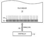
- FIG. 1illustrates an example touch sensor 10 with an example touch-sensor controller 12 .
- FIGS. 2A-2Cillustrate three example mesh patterns of a touch-sensitive mesh layer.
- FIG. 3illustrates a portion of an example electrode pattern.
- FIG. 4illustrates a portion of another example electrode pattern.
- FIG. 5illustrates an example mobile telephone that incorporates a touch sensor with conductive lines having portions with different widths.
- FIG. 1illustrates an example touch sensor 10 with an example touch-sensor controller 12 .
- Touch sensor 10 and touch-sensor controller 12may detect the presence and location of a touch or the proximity of an object within a touch-sensitive area of touch sensor 10 .
- reference to a touch sensormay encompass both the touch sensor and its touch-sensor controller, where appropriate.
- reference to a touch-sensor controllermay encompass both the touch-sensor controller and its touch sensor, where appropriate.
- Touch sensor 10may include one or more touch-sensitive areas, where appropriate.
- Touch sensor 10may include an array of drive and sense electrodes (or an array of electrodes of a single type) disposed on one or more substrates, which may be made of a dielectric material.
- reference to a touch sensormay encompass both the electrodes of the touch sensor and the substrate(s) that they are disposed on, where appropriate.
- reference to a touch sensormay encompass the electrodes of the touch sensor, but not the substrate(s) that they are disposed on.
- An electrodemay be an area of conductive material forming a shape, such as for example a disc, square, rectangle, other suitable shape, or suitable combination of these.
- One or more cuts in one or more layers of conductive materialmay (at least in part) create the shape of an electrode, and the area of the shape may (at least in part) be bounded by those cuts.
- the conductive material of an electrodemay occupy approximately 100% of the area of its shape.
- an electrodemay be made of indium tin oxide (ITO) and the ITO of the electrode may occupy approximately 100% of the area of its shape, where appropriate.
- ITOindium tin oxide
- the conductive material of an electrodemay occupy substantially less than 100% of the area of its shape.
- an electrodemay be made of fine lines of metal or other conductive material (FLM), such as for example copper, silver, or a copper- or silver-based material, and the fine lines of conductive material may occupy approximately 5% of the area of its shape in a hatched, mesh, or other suitable pattern.
- FLMconductive material
- this disclosuredescribes or illustrates particular electrodes made of particular conductive material forming particular shapes with particular fills having particular patterns, this disclosure contemplates any suitable electrodes made of any suitable conductive material forming any suitable shapes with any suitable fills having any suitable patterns.
- the shapes of the electrodes (or other elements) of a touch sensormay constitute in whole or in part one or more macro-features of the touch sensor.
- One or more characteristics of the implementation of those shapesmay constitute in whole or in part one or more micro-features of the touch sensor.
- One or more macro-features of a touch sensormay determine one or more characteristics of its functionality, and one or more micro-features of the touch sensor may determine one or more optical features of the touch sensor, such as transmittance, refraction, or reflection.
- a mechanical stackmay contain the substrate (or multiple substrates) and the conductive material forming the drive or sense electrodes of touch sensor 10 .
- the mechanical stackmay include a first layer of optically clear adhesive (OCA) beneath a cover panel.
- OCAoptically clear adhesive
- the cover panelmay be clear and made of a resilient material suitable for repeated touching, such as for example glass, polycarbonate, or poly(methyl methacrylate) (PMMA).
- PMMApoly(methyl methacrylate)
- This disclosurecontemplates any suitable cover panel made of any suitable material.
- the first layer of OCAmay be disposed between the cover panel and the substrate with the conductive material forming the drive or sense electrodes.
- the mechanical stackmay also include a second layer of OCA and a dielectric layer (which may be made of PET or another suitable material, similar to the substrate with the conductive material forming the drive or sense electrodes).
- a thin coating of a dielectric materialmay be applied instead of the second layer of OCA and the dielectric layer.
- the second layer of OCAmay be disposed between the substrate with the conductive material making up the drive or sense electrodes and the dielectric layer, and the dielectric layer may be disposed between the second layer of OCA and an air gap to a display of a device including touch sensor 10 and touch-sensor controller 12 .
- the cover panelmay have a thickness of approximately 1 mm; the first layer of OCA may have a thickness of approximately 0.05 mm; the substrate with the conductive material forming the drive or sense electrodes may have a thickness of approximately 0.05 mm; the second layer of OCA may have a thickness of approximately 0.05 mm; and the dielectric layer may have a thickness of approximately 0.05 mm.
- this disclosuredescribes a particular mechanical stack with a particular number of particular layers made of particular materials and having particular thicknesses, this disclosure contemplates any suitable mechanical stack with any suitable number of any suitable layers made of any suitable materials and having any suitable thicknesses.
- a layer of adhesive or dielectricmay replace the dielectric layer, second layer of OCA, and air gap described above, with there being no air gap to the display.
- One or more portions of the substrate of touch sensor 10may be made of polyethylene terephthalate (PET) or another suitable material. This disclosure contemplates any suitable substrate with any suitable portions made of any suitable material.
- the drive or sense electrodes in touch sensor 10may be made of ITO in whole or in part.
- the drive or sense electrodes in touch sensor 10may be made of fine lines of metal or other conductive material.
- one or more portions of the conductive materialmay be copper or copper-based and have a thickness of approximately 5 ⁇ m or less and a width of approximately 10 ⁇ m or less.
- one or more portions of the conductive materialmay be silver or silver-based and similarly have a thickness of approximately 5 ⁇ m or less and a width of approximately 10 ⁇ m or less. This disclosure contemplates any suitable electrodes made of any suitable material.
- Touch sensor 10may implement a capacitive form of touch sensing.
- touch sensor 10may include an array of drive and sense electrodes forming an array of capacitive nodes.
- a drive electrode and a sense electrodemay form a capacitive node.
- the drive and sense electrodes forming the capacitive nodemay come near each other, but not make electrical contact with each other. Instead, the drive and sense electrodes may be capacitively coupled to each other across a space between them.
- a pulsed or alternating voltage applied to the drive electrode(by touch-sensor controller 12 ) may induce a charge on the sense electrode, and the amount of charge induced may be susceptible to external influence (such as a touch or the proximity of an object).
- touch-sensor controller 12may measure the change in capacitance. By measuring changes in capacitance throughout the array, touch-sensor controller 12 may determine the position of the touch or proximity within the touch-sensitive area(s) of touch sensor 10 .
- touch sensor 10may include an array of electrodes of a single type that may each form a capacitive node.
- touch-sensor controller 12may measure the change in capacitance, for example, as a change in the amount of charge needed to raise the voltage at the capacitive node by a pre-determined amount.
- touch-sensor controller 12may determine the position of the touch or proximity within the touch-sensitive area(s) of touch sensor 10 .
- This disclosurecontemplates any suitable form of capacitive touch sensing, where appropriate.
- one or more drive electrodesmay together form a drive line running horizontally or vertically or in any suitable orientation.
- one or more sense electrodesmay together form a sense line running horizontally or vertically or in any suitable orientation.
- drive linesmay run substantially perpendicular to sense lines.
- reference to a drive linemay encompass one or more drive electrodes making up the drive line, and vice versa, where appropriate.
- reference to a sense linemay encompass one or more sense electrodes making up the sense line, and vice versa, where appropriate.
- Touch sensor 10may have drive and sense electrodes disposed in a pattern on one side of a single substrate. In such a configuration, a pair of drive and sense electrodes capacitively coupled to each other across a space between them may form a capacitive node. For a self-capacitance implementation, electrodes of only a single type may be disposed in a pattern on a single substrate. In addition or as an alternative to having drive and sense electrodes disposed in a pattern on one side of a single substrate, touch sensor 10 may have drive electrodes disposed in a pattern on one side of a substrate and sense electrodes disposed in a pattern on another side of the substrate.
- touch sensor 10may have drive electrodes disposed in a pattern on one side of one substrate and sense electrodes disposed in a pattern on one side of another substrate.
- an intersection of a drive electrode and a sense electrodemay form a capacitive node.
- Such an intersectionmay be a location where the drive electrode and the sense electrode “cross” or come nearest each other in their respective planes.
- the drive and sense electrodesdo not make electrical contact with each other—instead they are capacitively coupled to each other across a dielectric at the intersection.
- this disclosuredescribes particular configurations of particular electrodes forming particular nodes, this disclosure contemplates any suitable configuration of any suitable electrodes forming any suitable nodes. Moreover, this disclosure contemplates any suitable electrodes disposed on any suitable number of any suitable substrates in any suitable patterns.
- a change in capacitance at a capacitive node of touch sensor 10may indicate a touch or proximity input at the position of the capacitive node.
- Touch-sensor controller 12may detect and process the change in capacitance to determine the presence and location of the touch or proximity input. Touch-sensor controller 12 may then communicate information about the touch or proximity input to one or more other components (such one or more central processing units (CPUs) or digital signal processors (DSPs)) of a device that includes touch sensor 10 and touch-sensor controller 12 , which may respond to the touch or proximity input by initiating a function of the device (or an application running on the device) associated with it.
- CPUscentral processing units
- DSPsdigital signal processors
- Touch-sensor controller 12may be one or more integrated circuits (ICs), such as for example general-purpose microprocessors, microcontrollers, programmable logic devices or arrays, application-specific ICs (ASICs).
- touch-sensor controller 12comprises analog circuitry, digital logic, and digital non-volatile memory.
- touch-sensor controller 12is disposed on a flexible printed circuit (FPC) bonded to the substrate of touch sensor 10 , as described below.
- the FPCmay be active or passive, where appropriate.
- multiple touch-sensor controllers 12are disposed on the FPC.
- Touch-sensor controller 12may include a processor unit, a drive unit, a sense unit, and a storage unit.
- the drive unitmay supply drive signals to the drive electrodes of touch sensor 10 .
- the sense unitmay sense charge at the capacitive nodes of touch sensor 10 and provide measurement signals to the processor unit representing capacitances at the capacitive nodes.
- the processor unitmay control the supply of drive signals to the drive electrodes by the drive unit and process measurement signals from the sense unit to detect and process the presence and location of a touch or proximity input within the touch-sensitive area(s) of touch sensor 10 .
- the processor unitmay also track changes in the position of a touch or proximity input within the touch-sensitive area(s) of touch sensor 10 .
- the storage unitmay store programming for execution by the processor unit, including programming for controlling the drive unit to supply drive signals to the drive electrodes, programming for processing measurement signals from the sense unit, and other suitable programming, where appropriate.
- Tracks 14 of conductive material disposed on the substrate of touch sensor 10may couple the drive or sense electrodes of touch sensor 10 to connection pads 16 , also disposed on the substrate of touch sensor 10 . As described below, connection pads 16 facilitate coupling of tracks 14 to touch-sensor controller 12 . Tracks 14 may extend into or around (e.g. at the edges of) the touch-sensitive area(s) of touch sensor 10 . Particular tracks 14 may provide drive connections for coupling touch-sensor controller 12 to drive electrodes of touch sensor 10 , through which the drive unit of touch-sensor controller 12 may supply drive signals to the drive electrodes.
- Tracks 14may provide sense connections for coupling touch-sensor controller 12 to sense electrodes of touch sensor 10 , through which the sense unit of touch-sensor controller 12 may sense charge at the capacitive nodes of touch sensor 10 .
- Tracks 14may be made of fine lines of metal or other conductive material.
- the conductive material of tracks 14may be copper or copper-based and have a width of approximately 100 ⁇ m or less.
- the conductive material of tracks 14may be silver or silver-based and have a width of approximately 100 ⁇ m or less.
- tracks 14may be made of ITO in whole or in part in addition or as an alternative to fine lines of metal or other conductive material.
- touch sensor 10may include one or more ground lines terminating at a ground connector (which may be a connection pad 16 ) at an edge of the substrate of touch sensor 10 (similar to tracks 14 ).
- Connection pads 16may be located along one or more edges of the substrate, outside the touch-sensitive area(s) of touch sensor 10 .
- touch-sensor controller 12may be on an FPC.
- Connection pads 16may be made of the same material as tracks 14 and may be bonded to the FPC using an anisotropic conductive film (ACF).
- ACFanisotropic conductive film
- Connection 18may include conductive lines on the FPC coupling touch-sensor controller 12 to connection pads 16 , in turn coupling touch-sensor controller 12 to tracks 14 and to the drive or sense electrodes of touch sensor 10 .
- connection pads 16may be inserted into an electro-mechanical connector (such as a zero insertion force wire-to-board connector); in this embodiment, connection 18 may not need to include an FPC.
- This disclosurecontemplates any suitable connection 18 between touch-sensor controller 12 and touch sensor 10 .
- FIGS. 2A-2Cillustrate three example mesh patterns of a touch-sensitive mesh layer.
- an electrodemay be made of fine lines 22 A-B of metal or other conductive material (e.g., copper, silver, or a copper- or silver-based material) and the lines 22 A-B of conductive material may occupy the area of the electrode shape in a hatched, mesh, or other suitable pattern.
- an example mesh pattern 20 of a touch-sensitive mesh layeris formed from substantially straight lines 22 A-B of conductive material.
- Mesh pattern 20may be formed using two sets 22 A-B of substantially parallel lines of conductive material.
- Mesh pattern 20may be made up of an array of polygon-shaped mesh cells 24 formed from substantially orthogonal intersections between lines 22 A with lines 22 B of conductive material.
- first set 22 A and second set 22 B of conducting linesmay be disposed such that a total line density is less than approximately 10% of a surface area.
- the contribution of the conductive lines to the reduction of transmission of light through mesh pattern 20may be less than approximately 10%.
- the conductive linesmay result in an attenuation of, for example, 3-10% of the transmission of light through mesh pattern 20 .
- example mesh pattern 20 of a touch-sensitive mesh layerfurther includes one or more conductive lines 22 A-B that have a width that is greater than a width of one or more other conductive lines 22 A-B.
- mesh pattern 20may include a conductive line 26 and a conductive line 27 (which are examples of two of conductive lines 22 A-B).
- Conductive line 26may have a width that is greater than the width of conductive line 27 .
- conductive line 27may have any width that is less than the width of conductive line 26 .
- conductive line 27may have any width that is less than 5 ⁇ m, such as 4 ⁇ m, 3 ⁇ m, 2 ⁇ m, or any other width that is less than 5 ⁇ m.
- the total line density of example mesh pattern 20may be reduced.
- the reduced width of conductive line 27may increase the transmittance in a device utilizing example mesh pattern 20 .
- example mesh pattern 20 of a touch-sensitive mesh layerfurther includes one or more electrodes, such as, for example, electrode 28 .
- electrode 28may include a plurality of conductive lines 22 A-B.
- one or more of the conductive lines 22 A-Bmay be primary conductive lines while one or more of the conductive lines 22 A-B may be secondary conductive lines.
- the width of the secondary conductive linesmay be less than that of the primary conductive lines.
- conductive line 26(which may have a width that is greater than that of conductive line 27 ) may be a primary conductive line, while conductive line 27 may be a secondary conductive line.
- Electrode 28may have any suitable pattern for the primary conductive lines and secondary conductive lines. As an example and not by way of limitation, the primary conductive lines of electrode 28 may be the outermost conductive lines of electrode 28 , while the secondary conductive lines of electrode 28 may be the innermost conductive lines of electrode 28 .
- a mesh patternmay include any particular pattern of conductive lines, any particular pattern of primary conductive lines, any particular pattern of secondary conductive lines, and any particular pattern of electrodes.
- mesh pattern 30is formed from conductive lines 32 A-B which are not substantially straight.
- Non-straight line patterns 32 A-Bmay be used to reduce the likelihood of the metal line patterns causing interference or moiré patterns.
- the non-straight pattern of the conductive lines 32 A-B of mesh pattern 30may disperse—and hence reduce—the visibility of reflections from conductive lines 32 A-B when illuminated by incident light.
- each of conductive lines 32 A-B of mesh pattern 30may have a substantially wavy, or sinusoidal, shape, as shown in FIG. 2B .
- Mesh pattern 30may be made up of an array of mesh cells 33 formed from intersections between lines 32 A with lines 32 B of conductive material.
- example mesh pattern 30 of a touch-sensitive mesh layerfurther includes one or more conductive lines 32 A-B that have a width that is greater than a width of one or more other conductive lines 32 A-B (such as conductive line 34 having a greater width than the width of conductive line 35 ).
- Mesh pattern 30further includes one or more electrodes, such as, for example, electrode 36 .
- the electrodes of mesh pattern 30may have primary conductive lines and secondary conductive lines, where the primary conductive lines (such as, for example, conductive line 34 ) have a width that is greater than the width of the secondary conductive lines (such as, for example, conductive line 35 ).
- a mesh patternmay include any particular pattern of conductive lines, any particular pattern of primary conductive lines, any particular pattern of secondary conductive lines, and any particular pattern of electrodes.
- mesh pattern 40is formed from conductive lines 42 A-B which are substantially straight.
- Mesh pattern 40may be made up of an array of mesh cells 44 formed from intersections between lines 42 A with lines 42 B of conductive material.
- example mesh pattern 40 of a touch-sensitive mesh layerfurther includes one or more conductive lines 42 A-B that have at least one portion with a width that is greater than a width at least one other portion of the same conductive line 42 A-B.
- mesh pattern 40may include a conductive line 46 and a conductive line 47 (which are examples of two of conductive lines 42 A-B).
- Conductive lines 46 and 47each include three portions: a first portion (such as first portions 46 A and 47 A), a second portion (such as second portions 46 B and 47 B), and a third portion (such as third portions 46 C and 47 C).
- First portions 46 A and 47 A and third portions 46 C and 47 Cmay each have widths (not necessarily equal to each other) that are greater than the width of each of second portions 46 B and 47 B.
- second portions 46 B and 47 Bmay each have any width that is less than 5 ⁇ m, such as 4 ⁇ m, 3 ⁇ m, 2 ⁇ m, or any other width that is less than 5 ⁇ m.
- second portions 46 B and 47 Bmay each have any width that is less than 3 ⁇ m, such as 2 ⁇ m, or any other width that is less than 3 ⁇ m.
- each of second portions 46 B and 47 Bmay be less than the width of each of first portions 46 A and 47 A and third portions 46 C and 47 C, the total line density of example mesh pattern 40 may be reduced. As such, the reduced width of second portions 46 B and 47 B may increase the transmittance in a device utilizing example mesh pattern 40 .
- example mesh pattern 40 of a touch-sensitive mesh layerfurther includes one or more electrodes, such as, for example, electrode 48 .
- electrode 48may include a plurality of conductive lines 42 A-B.
- the first portions of conductive lines 42 A-B and third portions of conductive lines 42 A-Bmay define a portion of each of the outer edges of the electrodes.
- first portion 46 Amay define a first portion of a first outer edge of electrode 48 and first portion 47 A may define a second portion of the first outer edge of electrode 48 .
- third portion 46 Cmay define a first portion of a second outer edge of electrode 48 and third portion 47 C may define a second portion of the second outer edge of electrode 48 .
- the outer edges of the electrodes, such as electrode 48may be the edges that define the shape of each electrode and/or the main area of each electrode.
- the outer edges of the electrodesmay be primary conductive areas while the inner portions of the electrodes (such as the inner portions made up of second portions of conductive lines 42 A-B) may be secondary conductive areas.
- the primary conductive areassince the primary conductive areas have a greater width than that of the secondary conductive areas, if one or more portions of the secondary conductive areas break (or are otherwise unable to carry an alternating voltage or charge), the primary conductive areas and the remaining portions of the secondary conductive areas may still carry the alternating voltage applied to a drive electrode or the charge induced on a sense electrode. As such, the primary conductive areas and remaining portions of secondary conductive areas may still provide a suitable level of electrical connectivity across mesh pattern 40 .
- Electrode 48may have any suitable pattern for the primary conductive areas and secondary conductive areas.
- portions of conductive lines 42 A-Bmay be cut in-between electrodes, such as electrode 48 . These cut portions of conductive lines 42 A-B may be boundary separation lines that separate an electrode from an adjacent electrode. Furthermore, these cut portions may also form each electrode. Although this disclosure describes or illustrates conductive lines 42 A-B as having portions in-between each electrode that have been cut (e.g., thus forming each electrode), conductive lines 42 A-B need not have been cut in order to form the electrodes. As an example and not by way of limitation, one or more of the electrodes may be printed (or otherwise formed) on a substrate in a manner that does not require any cuts to be made in order to form the electrodes. In such an example, there need not be any portions of conductive lines 42 A-B in-between each electrode and/or the portions of conductive lines 42 A-B in-between each electrode may be reduced in size.
- a mesh patternmay include any particular pattern of conductive lines, any particular pattern of portions of conductive lines, any particular pattern of primary conductive areas, any particular pattern of secondary conductive areas, and any particular pattern of electrodes.
- conductive lines 42 A-Bmay have any other shape. As an example and not by way of limitation, conductive lines 42 A-B may be not substantially straight. Additionally, although this disclosure describes or illustrates the electrodes, such as electrode 48 , as including two outermost edges, the electrodes may have any number of outermost edges. As an example and not by way of limitation, the electrodes may have only one outermost edge. As other examples and not by way of limitation, the electrodes may have three outermost edges, four outermost edges, or any other number of outermost edges.
- FIG. 3illustrates a portion of an example electrode pattern 50 .
- the electrode pattern 50includes a conductive line 51 that is not substantially straight.
- the conductive line 51includes narrow portions 51 A and broader portions 51 B.
- the conductive line 51may have a tapering width between the narrow portions 51 A and broader portions 51 B. In other examples, the width can vary non-linearly along the length of the conductive line 51 .
- FIG. 4illustrates a portion of another example electrode pattern 60 .
- the electrode pattern 60is formed by conductive lines 61 arranged to interconnect at a connection point 62 to define a conductive grid or mesh pattern made up of an array of mesh cells.
- the connection point 62 of the conductive lines 61forms a vertex of four of the shapes.
- a single connection point 62is shown, together with parts of the conductive lines 61 which interconnect at the connection point 62 .
- each of the four conductive lines 61are relatively narrow at the connection point 62 , and relatively broad away from the connection point 62 .
- Each of the conductive lines 61may have a tapered section which widens in a direction extending away from the connection point 62 .
- the conductive linesmay vary in width along their length and may be relatively narrow where the conductive lines interconnect at a connection point.
- the conductive linesare not substantially straight.
- the conductive linescould have other shapes.
- the conductive lines which vary in width along their length and/or the conductive lines which may be narrowed where the conductive lines interconnectcould be conductive lines that are substantially straight.
- reducing the width of the conductive lines in the respective electrode patterns in the two electrode layers where the conductive lines cross overmay reduce visible reductions in display brightness at the interconnections. Such reductions in display brightness may be visible where constant width conductive lines cross over as there may be a concentration of conductive metal at the cross over point. Reducing the width of the conductive lines where the conductive lines cross over may make the distribution of the conductive metal across a touch position sensing panel more even, reducing the visibility of differences in display brightness.
- FIG. 5illustrates an example mobile telephone that incorporates a touch sensor with conductive lines having portions with different widths.
- example mobile telephone 100incorporates a touch-sensitive apparatus 112 wrapped around an example display 113 .
- Substrate 102may include or have attached to it tracking areas, which may include tracks providing drive and sense connections to and from the drive and sense electrodes of touch-sensitive apparatus 112 .
- an electrode pattern of touch-sensitive apparatus 112is made from metal-mesh technology with a copper, silver, or other suitable metal mesh, as described above.
- Substrate 102may have the electrode pattern disposed on a surface.
- Substrate 102 and the conductive material of the electrode patternmay be flexible, enabling the conductive material to wrap around the left and right edges of the surface to left-side and right-side surfaces.
- the flexible conductive material of the electrode patternmay be thicker or wider at the sharper edges than at the flat portions of surfaces.
- the electrode patternmay wrap around an edge 103 of example mobile phone 100 .
- touch-sensitive apparatus 112may be wrapped around a curved surface.
- the curved surfacemay be curved in one dimension or in two dimensions.
- touch-sensitive apparatus 112may be wrapped over surfaces that are substantially perpendicular to each other or, if there is no substantial distinction between surfaces (such as, for example, a pebble-shaped or curved device), an angle of deviation between the surfaces of 45° or greater.
- this disclosuredescribes and illustrates a particular use of touch-sensitive apparatus 112 in a particular device, this disclosure contemplates any suitable use of touch-sensitive apparatus 112 in any suitable device.
- Example display 113may be a liquid crystal display (LCD), a light-emitting diode (LED) display, an LED-backlight LCD, or other suitable display and may be visible though cover panel 101 and substrate 102 , as well as the electrode pattern disposed on substrate 102 .
- LCDliquid crystal display
- LEDlight-emitting diode
- LED-backlight LCDLED-backlight LCD
- this disclosuredescribes and illustrates a particular display and particular display types, this disclosure contemplates any suitable device display and any suitable display types.
- a computer-readable storage medium or mediamay include one or more semiconductor-based or other integrated circuits (ICs) (such, as for example, a field-programmable gate array (FPGA) or an application-specific IC (ASIC)), hard disk drives (HDDs), hybrid hard drives (HHDs), optical discs, optical disc drives (ODDs), magneto-optical discs, magneto-optical drives, floppy disks, floppy disk drives (FDDs), magnetic tapes, holographic storage media, solid-state drives (SSDs), RAM-drives, SECURE DIGITAL cards, SECURE DIGITAL drives, or any other suitable computer-readable storage medium or media, or any suitable combination of two or more of these, where appropriate.
- ICssuch, as for example, a field-programmable gate array (FPGA) or an application-specific IC (ASIC)
- HDDshard disk drives
- HHDshybrid hard drives
- ODDsoptical disc drives
- magneto-optical discsmagneto-optical
Landscapes
- Engineering & Computer Science (AREA)
- General Engineering & Computer Science (AREA)
- Theoretical Computer Science (AREA)
- Human Computer Interaction (AREA)
- Physics & Mathematics (AREA)
- General Physics & Mathematics (AREA)
- Position Input By Displaying (AREA)
Abstract
Description
- This disclosure generally relates to touch sensors.
- A touch sensor may detect the presence and location of a touch or the proximity of an object (such as a user's finger or a stylus) within a touch-sensitive area of the touch sensor overlaid on a display screen, for example. In a touch-sensitive-display application, the touch sensor may enable a user to interact directly with what is displayed on the screen, rather than indirectly with a mouse or touch pad. A touch sensor may be attached to or provided as part of a desktop computer, laptop computer, tablet computer, personal digital assistant (PDA), smartphone, satellite navigation device, portable media player, portable game console, kiosk computer, point-of-sale device, or other suitable device. A control panel on a household or other appliance may include a touch sensor.
- There are a number of different types of touch sensors, such as (for example) resistive touch screens, surface acoustic wave touch screens, and capacitive touch screens. Herein, reference to a touch sensor may encompass a touch screen, and vice versa, where appropriate. When an object touches or comes within proximity of the surface of the capacitive touch screen, a change in capacitance may occur within the touch screen at the location of the touch or proximity. A touch-sensor controller may process the change in capacitance to determine its position on the touch screen.
FIG. 1 illustrates anexample touch sensor 10 with an example touch-sensor controller 12.FIGS. 2A-2C illustrate three example mesh patterns of a touch-sensitive mesh layer.FIG. 3 illustrates a portion of an example electrode pattern.FIG. 4 illustrates a portion of another example electrode pattern.FIG. 5 illustrates an example mobile telephone that incorporates a touch sensor with conductive lines having portions with different widths.FIG. 1 illustrates anexample touch sensor 10 with an example touch-sensor controller 12.Touch sensor 10 and touch-sensor controller 12 may detect the presence and location of a touch or the proximity of an object within a touch-sensitive area oftouch sensor 10. Herein, reference to a touch sensor may encompass both the touch sensor and its touch-sensor controller, where appropriate. Similarly, reference to a touch-sensor controller may encompass both the touch-sensor controller and its touch sensor, where appropriate.Touch sensor 10 may include one or more touch-sensitive areas, where appropriate.Touch sensor 10 may include an array of drive and sense electrodes (or an array of electrodes of a single type) disposed on one or more substrates, which may be made of a dielectric material. Herein, reference to a touch sensor may encompass both the electrodes of the touch sensor and the substrate(s) that they are disposed on, where appropriate. Alternatively, where appropriate, reference to a touch sensor may encompass the electrodes of the touch sensor, but not the substrate(s) that they are disposed on.- An electrode (whether a drive electrode or a sense electrode) may be an area of conductive material forming a shape, such as for example a disc, square, rectangle, other suitable shape, or suitable combination of these. One or more cuts in one or more layers of conductive material may (at least in part) create the shape of an electrode, and the area of the shape may (at least in part) be bounded by those cuts. In particular embodiments, the conductive material of an electrode may occupy approximately 100% of the area of its shape. As an example and not by way of limitation, an electrode may be made of indium tin oxide (ITO) and the ITO of the electrode may occupy approximately 100% of the area of its shape, where appropriate. In particular embodiments, the conductive material of an electrode may occupy substantially less than 100% of the area of its shape. As an example and not by way of limitation, an electrode may be made of fine lines of metal or other conductive material (FLM), such as for example copper, silver, or a copper- or silver-based material, and the fine lines of conductive material may occupy approximately 5% of the area of its shape in a hatched, mesh, or other suitable pattern. Herein, reference to FLM encompasses such material, where appropriate. Although this disclosure describes or illustrates particular electrodes made of particular conductive material forming particular shapes with particular fills having particular patterns, this disclosure contemplates any suitable electrodes made of any suitable conductive material forming any suitable shapes with any suitable fills having any suitable patterns. Where appropriate, the shapes of the electrodes (or other elements) of a touch sensor may constitute in whole or in part one or more macro-features of the touch sensor. One or more characteristics of the implementation of those shapes (such as, for example, the conductive materials, fills, or patterns within the shapes) may constitute in whole or in part one or more micro-features of the touch sensor. One or more macro-features of a touch sensor may determine one or more characteristics of its functionality, and one or more micro-features of the touch sensor may determine one or more optical features of the touch sensor, such as transmittance, refraction, or reflection.
- A mechanical stack may contain the substrate (or multiple substrates) and the conductive material forming the drive or sense electrodes of
touch sensor 10. As an example and not by way of limitation, the mechanical stack may include a first layer of optically clear adhesive (OCA) beneath a cover panel. The cover panel may be clear and made of a resilient material suitable for repeated touching, such as for example glass, polycarbonate, or poly(methyl methacrylate) (PMMA). This disclosure contemplates any suitable cover panel made of any suitable material. The first layer of OCA may be disposed between the cover panel and the substrate with the conductive material forming the drive or sense electrodes. The mechanical stack may also include a second layer of OCA and a dielectric layer (which may be made of PET or another suitable material, similar to the substrate with the conductive material forming the drive or sense electrodes). As an alternative, where appropriate, a thin coating of a dielectric material may be applied instead of the second layer of OCA and the dielectric layer. The second layer of OCA may be disposed between the substrate with the conductive material making up the drive or sense electrodes and the dielectric layer, and the dielectric layer may be disposed between the second layer of OCA and an air gap to a display of a device includingtouch sensor 10 and touch-sensor controller 12. As an example only and not by way of limitation, the cover panel may have a thickness of approximately 1 mm; the first layer of OCA may have a thickness of approximately 0.05 mm; the substrate with the conductive material forming the drive or sense electrodes may have a thickness of approximately 0.05 mm; the second layer of OCA may have a thickness of approximately 0.05 mm; and the dielectric layer may have a thickness of approximately 0.05 mm. Although this disclosure describes a particular mechanical stack with a particular number of particular layers made of particular materials and having particular thicknesses, this disclosure contemplates any suitable mechanical stack with any suitable number of any suitable layers made of any suitable materials and having any suitable thicknesses. As an example and not by way of limitation, in particular embodiments, a layer of adhesive or dielectric may replace the dielectric layer, second layer of OCA, and air gap described above, with there being no air gap to the display. - One or more portions of the substrate of
touch sensor 10 may be made of polyethylene terephthalate (PET) or another suitable material. This disclosure contemplates any suitable substrate with any suitable portions made of any suitable material. In particular embodiments, the drive or sense electrodes intouch sensor 10 may be made of ITO in whole or in part. In particular embodiments, the drive or sense electrodes intouch sensor 10 may be made of fine lines of metal or other conductive material. As an example and not by way of limitation, one or more portions of the conductive material may be copper or copper-based and have a thickness of approximately 5 μm or less and a width of approximately 10 μm or less. As another example, one or more portions of the conductive material may be silver or silver-based and similarly have a thickness of approximately 5 μm or less and a width of approximately 10 μm or less. This disclosure contemplates any suitable electrodes made of any suitable material. Touch sensor 10 may implement a capacitive form of touch sensing. In a mutual-capacitance implementation,touch sensor 10 may include an array of drive and sense electrodes forming an array of capacitive nodes. A drive electrode and a sense electrode may form a capacitive node. The drive and sense electrodes forming the capacitive node may come near each other, but not make electrical contact with each other. Instead, the drive and sense electrodes may be capacitively coupled to each other across a space between them. A pulsed or alternating voltage applied to the drive electrode (by touch-sensor controller12) may induce a charge on the sense electrode, and the amount of charge induced may be susceptible to external influence (such as a touch or the proximity of an object). When an object touches or comes within proximity of the capacitive node, a change in capacitance may occur at the capacitive node and touch-sensor controller 12 may measure the change in capacitance. By measuring changes in capacitance throughout the array, touch-sensor controller 12 may determine the position of the touch or proximity within the touch-sensitive area(s) oftouch sensor 10.- In a self-capacitance implementation,
touch sensor 10 may include an array of electrodes of a single type that may each form a capacitive node. When an object touches or comes within proximity of the capacitive node, a change in self-capacitance may occur at the capacitive node and touch-sensor controller 12 may measure the change in capacitance, for example, as a change in the amount of charge needed to raise the voltage at the capacitive node by a pre-determined amount. As with a mutual-capacitance implementation, by measuring changes in capacitance throughout the array, touch-sensor controller 12 may determine the position of the touch or proximity within the touch-sensitive area(s) oftouch sensor 10. This disclosure contemplates any suitable form of capacitive touch sensing, where appropriate. - In particular embodiments, one or more drive electrodes may together form a drive line running horizontally or vertically or in any suitable orientation. Similarly, one or more sense electrodes may together form a sense line running horizontally or vertically or in any suitable orientation. In particular embodiments, drive lines may run substantially perpendicular to sense lines. Herein, reference to a drive line may encompass one or more drive electrodes making up the drive line, and vice versa, where appropriate. Similarly, reference to a sense line may encompass one or more sense electrodes making up the sense line, and vice versa, where appropriate.
Touch sensor 10 may have drive and sense electrodes disposed in a pattern on one side of a single substrate. In such a configuration, a pair of drive and sense electrodes capacitively coupled to each other across a space between them may form a capacitive node. For a self-capacitance implementation, electrodes of only a single type may be disposed in a pattern on a single substrate. In addition or as an alternative to having drive and sense electrodes disposed in a pattern on one side of a single substrate,touch sensor 10 may have drive electrodes disposed in a pattern on one side of a substrate and sense electrodes disposed in a pattern on another side of the substrate. Moreover,touch sensor 10 may have drive electrodes disposed in a pattern on one side of one substrate and sense electrodes disposed in a pattern on one side of another substrate. In such configurations, an intersection of a drive electrode and a sense electrode may form a capacitive node. Such an intersection may be a location where the drive electrode and the sense electrode “cross” or come nearest each other in their respective planes. The drive and sense electrodes do not make electrical contact with each other—instead they are capacitively coupled to each other across a dielectric at the intersection. Although this disclosure describes particular configurations of particular electrodes forming particular nodes, this disclosure contemplates any suitable configuration of any suitable electrodes forming any suitable nodes. Moreover, this disclosure contemplates any suitable electrodes disposed on any suitable number of any suitable substrates in any suitable patterns.- As described above, a change in capacitance at a capacitive node of
touch sensor 10 may indicate a touch or proximity input at the position of the capacitive node. Touch-sensor controller 12 may detect and process the change in capacitance to determine the presence and location of the touch or proximity input. Touch-sensor controller 12 may then communicate information about the touch or proximity input to one or more other components (such one or more central processing units (CPUs) or digital signal processors (DSPs)) of a device that includestouch sensor 10 and touch-sensor controller 12, which may respond to the touch or proximity input by initiating a function of the device (or an application running on the device) associated with it. Although this disclosure describes a particular touch-sensor controller having particular functionality with respect to a particular device and a particular touch sensor, this disclosure contemplates any suitable touch-sensor controller having any suitable functionality with respect to any suitable device and any suitable touch sensor. - Touch-
sensor controller 12 may be one or more integrated circuits (ICs), such as for example general-purpose microprocessors, microcontrollers, programmable logic devices or arrays, application-specific ICs (ASICs). In particular embodiments, touch-sensor controller 12 comprises analog circuitry, digital logic, and digital non-volatile memory. In particular embodiments, touch-sensor controller 12 is disposed on a flexible printed circuit (FPC) bonded to the substrate oftouch sensor 10, as described below. The FPC may be active or passive, where appropriate. In particular embodiments, multiple touch-sensor controllers 12 are disposed on the FPC. Touch-sensor controller 12 may include a processor unit, a drive unit, a sense unit, and a storage unit. The drive unit may supply drive signals to the drive electrodes oftouch sensor 10. The sense unit may sense charge at the capacitive nodes oftouch sensor 10 and provide measurement signals to the processor unit representing capacitances at the capacitive nodes. The processor unit may control the supply of drive signals to the drive electrodes by the drive unit and process measurement signals from the sense unit to detect and process the presence and location of a touch or proximity input within the touch-sensitive area(s) oftouch sensor 10. The processor unit may also track changes in the position of a touch or proximity input within the touch-sensitive area(s) oftouch sensor 10. The storage unit may store programming for execution by the processor unit, including programming for controlling the drive unit to supply drive signals to the drive electrodes, programming for processing measurement signals from the sense unit, and other suitable programming, where appropriate. Although this disclosure describes a particular touch-sensor controller having a particular implementation with particular components, this disclosure contemplates any suitable touch-sensor controller having any suitable implementation with any suitable components. Tracks 14 of conductive material disposed on the substrate oftouch sensor 10 may couple the drive or sense electrodes oftouch sensor 10 toconnection pads 16, also disposed on the substrate oftouch sensor 10. As described below,connection pads 16 facilitate coupling oftracks 14 to touch-sensor controller 12.Tracks 14 may extend into or around (e.g. at the edges of) the touch-sensitive area(s) oftouch sensor 10.Particular tracks 14 may provide drive connections for coupling touch-sensor controller 12 to drive electrodes oftouch sensor 10, through which the drive unit of touch-sensor controller 12 may supply drive signals to the drive electrodes.Other tracks 14 may provide sense connections for coupling touch-sensor controller 12 to sense electrodes oftouch sensor 10, through which the sense unit of touch-sensor controller 12 may sense charge at the capacitive nodes oftouch sensor 10.Tracks 14 may be made of fine lines of metal or other conductive material. As an example and not by way of limitation, the conductive material oftracks 14 may be copper or copper-based and have a width of approximately 100 μm or less. As another example, the conductive material oftracks 14 may be silver or silver-based and have a width of approximately 100 μm or less. In particular embodiments, tracks14 may be made of ITO in whole or in part in addition or as an alternative to fine lines of metal or other conductive material. Although this disclosure describes particular tracks made of particular materials with particular widths, this disclosure contemplates any suitable tracks made of any suitable materials with any suitable widths. In addition totracks 14,touch sensor 10 may include one or more ground lines terminating at a ground connector (which may be a connection pad16) at an edge of the substrate of touch sensor10 (similar to tracks14).Connection pads 16 may be located along one or more edges of the substrate, outside the touch-sensitive area(s) oftouch sensor 10. As described above, touch-sensor controller 12 may be on an FPC.Connection pads 16 may be made of the same material astracks 14 and may be bonded to the FPC using an anisotropic conductive film (ACF).Connection 18 may include conductive lines on the FPC coupling touch-sensor controller 12 toconnection pads 16, in turn coupling touch-sensor controller 12 totracks 14 and to the drive or sense electrodes oftouch sensor 10. In another embodiment,connection pads 16 may be inserted into an electro-mechanical connector (such as a zero insertion force wire-to-board connector); in this embodiment,connection 18 may not need to include an FPC. This disclosure contemplates anysuitable connection 18 between touch-sensor controller 12 andtouch sensor 10.FIGS. 2A-2C illustrate three example mesh patterns of a touch-sensitive mesh layer. As discussed above, an electrode may be made offine lines 22A-B of metal or other conductive material (e.g., copper, silver, or a copper- or silver-based material) and thelines 22A-B of conductive material may occupy the area of the electrode shape in a hatched, mesh, or other suitable pattern. In the example ofFIG. 2A , anexample mesh pattern 20 of a touch-sensitive mesh layer is formed from substantiallystraight lines 22A-B of conductive material.Mesh pattern 20 may be formed using twosets 22A-B of substantially parallel lines of conductive material.Mesh pattern 20 may be made up of an array of polygon-shapedmesh cells 24 formed from substantially orthogonal intersections betweenlines 22A withlines 22B of conductive material. As an example and not by way of limitation,first set 22A andsecond set 22B of conducting lines may be disposed such that a total line density is less than approximately 10% of a surface area. Thus, the contribution of the conductive lines to the reduction of transmission of light throughmesh pattern 20 may be less than approximately 10%. In particular embodiments, the conductive lines may result in an attenuation of, for example, 3-10% of the transmission of light throughmesh pattern 20.- In the example of
FIG. 2A ,example mesh pattern 20 of a touch-sensitive mesh layer further includes one or moreconductive lines 22A-B that have a width that is greater than a width of one or more otherconductive lines 22A-B. As an example and not by way of limitation,mesh pattern 20 may include aconductive line 26 and a conductive line27 (which are examples of two ofconductive lines 22A-B).Conductive line 26 may have a width that is greater than the width ofconductive line 27. In particular embodiments,conductive line 27 may have any width that is less than the width ofconductive line 26. As an example and not by way of limitation, if the width ofconductive line 26 is 5 μm,conductive line 27 may have any width that is less than 5 μm, such as 4 μm, 3 μm, 2 μm, or any other width that is less than 5 μm. In particular embodiments, becauseconductive line 27 has a width that is less than the width ofconductive line 26, the total line density ofexample mesh pattern 20 may be reduced. As such, the reduced width ofconductive line 27 may increase the transmittance in a device utilizingexample mesh pattern 20. - In the example of
FIG. 2A ,example mesh pattern 20 of a touch-sensitive mesh layer further includes one or more electrodes, such as, for example,electrode 28. In particular embodiments,electrode 28 may include a plurality ofconductive lines 22A-B. Furthermore, in particular embodiments, one or more of theconductive lines 22A-B may be primary conductive lines while one or more of theconductive lines 22A-B may be secondary conductive lines. In particular embodiments, the width of the secondary conductive lines may be less than that of the primary conductive lines. As an example and not by way of limitation, conductive line26 (which may have a width that is greater than that of conductive line27) may be a primary conductive line, whileconductive line 27 may be a secondary conductive line. In particular embodiments, since the primary conductive lines have a greater width than that of the secondary conductive lines, if one or more of the secondary conductive lines break (or are otherwise unable to carry an alternating voltage or charge), the primary conductive lines and the remaining secondary conductive lines may still carry the alternating voltage applied to a drive electrode or the charge induced on a sense electrode. As such, the primary conductive lines and remaining secondary conductive lines may still provide a suitable level of electrical connectivity acrossmesh pattern 20.Electrode 28 may have any suitable pattern for the primary conductive lines and secondary conductive lines. As an example and not by way of limitation, the primary conductive lines ofelectrode 28 may be the outermost conductive lines ofelectrode 28, while the secondary conductive lines ofelectrode 28 may be the innermost conductive lines ofelectrode 28. - Although this disclosure describes or illustrates particular mesh patterns, this disclosure contemplates any suitable mesh pattern formed using conductive lines with any suitable configuration. As an example and not by way of limitation, a mesh pattern may include any particular pattern of conductive lines, any particular pattern of primary conductive lines, any particular pattern of secondary conductive lines, and any particular pattern of electrodes.
- In the example of
FIG. 2B ,mesh pattern 30 is formed fromconductive lines 32A-B which are not substantially straight.Non-straight line patterns 32A-B may be used to reduce the likelihood of the metal line patterns causing interference or moiré patterns. The non-straight pattern of theconductive lines 32A-B ofmesh pattern 30 may disperse—and hence reduce—the visibility of reflections fromconductive lines 32A-B when illuminated by incident light. As an example and not by way of limitation, each ofconductive lines 32A-B ofmesh pattern 30 may have a substantially wavy, or sinusoidal, shape, as shown inFIG. 2B .Mesh pattern 30 may be made up of an array ofmesh cells 33 formed from intersections betweenlines 32A withlines 32B of conductive material. - In the example of
FIG. 2B ,example mesh pattern 30 of a touch-sensitive mesh layer further includes one or moreconductive lines 32A-B that have a width that is greater than a width of one or more otherconductive lines 32A-B (such asconductive line 34 having a greater width than the width of conductive line35).Mesh pattern 30 further includes one or more electrodes, such as, for example,electrode 36. Furthermore, the electrodes ofmesh pattern 30 may have primary conductive lines and secondary conductive lines, where the primary conductive lines (such as, for example, conductive line34) have a width that is greater than the width of the secondary conductive lines (such as, for example, conductive line35). - Although this disclosure describes or illustrates particular mesh patterns, this disclosure contemplates any suitable mesh pattern formed using conductive lines with any suitable configuration. As an example and not by way of limitation, a mesh pattern may include any particular pattern of conductive lines, any particular pattern of primary conductive lines, any particular pattern of secondary conductive lines, and any particular pattern of electrodes.
- In the example of
FIG. 2C ,mesh pattern 40 is formed fromconductive lines 42A-B which are substantially straight.Mesh pattern 40 may be made up of an array ofmesh cells 44 formed from intersections betweenlines 42A withlines 42B of conductive material. - In the example of
FIG. 2C ,example mesh pattern 40 of a touch-sensitive mesh layer further includes one or moreconductive lines 42A-B that have at least one portion with a width that is greater than a width at least one other portion of the sameconductive line 42A-B. As an example and not by way of limitation,mesh pattern 40 may include aconductive line 46 and a conductive line47 (which are examples of two ofconductive lines 42A-B).Conductive lines first portions second portions third portions First portions third portions second portions - As an example and not by way of limitation, if the width of each of
first portions third portions second portions first portions third portions second portions second portions first portions third portions example mesh pattern 40 may be reduced. As such, the reduced width ofsecond portions example mesh pattern 40. - In the example of
FIG. 2C ,example mesh pattern 40 of a touch-sensitive mesh layer further includes one or more electrodes, such as, for example,electrode 48. In particular embodiments,electrode 48 may include a plurality ofconductive lines 42A-B. Furthermore, in particular embodiments, the first portions ofconductive lines 42A-B and third portions ofconductive lines 42A-B may define a portion of each of the outer edges of the electrodes. As an example and not by way of limitation,first portion 46A may define a first portion of a first outer edge ofelectrode 48 andfirst portion 47A may define a second portion of the first outer edge ofelectrode 48. As another example and not by way of limitation,third portion 46C may define a first portion of a second outer edge ofelectrode 48 andthird portion 47C may define a second portion of the second outer edge ofelectrode 48. The outer edges of the electrodes, such aselectrode 48, may be the edges that define the shape of each electrode and/or the main area of each electrode. - In particular embodiments, the outer edges of the electrodes may be primary conductive areas while the inner portions of the electrodes (such as the inner portions made up of second portions of
conductive lines 42A-B) may be secondary conductive areas. In particular embodiments, since the primary conductive areas have a greater width than that of the secondary conductive areas, if one or more portions of the secondary conductive areas break (or are otherwise unable to carry an alternating voltage or charge), the primary conductive areas and the remaining portions of the secondary conductive areas may still carry the alternating voltage applied to a drive electrode or the charge induced on a sense electrode. As such, the primary conductive areas and remaining portions of secondary conductive areas may still provide a suitable level of electrical connectivity acrossmesh pattern 40.Electrode 48 may have any suitable pattern for the primary conductive areas and secondary conductive areas. - According to the illustrated embodiment, portions of
conductive lines 42A-B may be cut in-between electrodes, such aselectrode 48. These cut portions ofconductive lines 42A-B may be boundary separation lines that separate an electrode from an adjacent electrode. Furthermore, these cut portions may also form each electrode. Although this disclosure describes or illustratesconductive lines 42A-B as having portions in-between each electrode that have been cut (e.g., thus forming each electrode),conductive lines 42A-B need not have been cut in order to form the electrodes. As an example and not by way of limitation, one or more of the electrodes may be printed (or otherwise formed) on a substrate in a manner that does not require any cuts to be made in order to form the electrodes. In such an example, there need not be any portions ofconductive lines 42A-B in-between each electrode and/or the portions ofconductive lines 42A-B in-between each electrode may be reduced in size. - Furthermore, although this disclosure describes or illustrates particular mesh patterns, this disclosure contemplates any suitable mesh pattern formed using conductive lines with any suitable configuration. As an example and not by way of limitation, a mesh pattern may include any particular pattern of conductive lines, any particular pattern of portions of conductive lines, any particular pattern of primary conductive areas, any particular pattern of secondary conductive areas, and any particular pattern of electrodes.
- Additionally, although this disclosure describes or illustrates
conductive lines 42A-B as being substantially straight,conductive lines 42A-B may have any other shape. As an example and not by way of limitation,conductive lines 42A-B may be not substantially straight. Additionally, although this disclosure describes or illustrates the electrodes, such aselectrode 48, as including two outermost edges, the electrodes may have any number of outermost edges. As an example and not by way of limitation, the electrodes may have only one outermost edge. As other examples and not by way of limitation, the electrodes may have three outermost edges, four outermost edges, or any other number of outermost edges. FIG. 3 illustrates a portion of anexample electrode pattern 50. In this example, theelectrode pattern 50 includes aconductive line 51 that is not substantially straight. Theconductive line 51 includesnarrow portions 51A andbroader portions 51B. Theconductive line 51 may have a tapering width between thenarrow portions 51A andbroader portions 51B. In other examples, the width can vary non-linearly along the length of theconductive line 51.FIG. 4 illustrates a portion of anotherexample electrode pattern 60. In this illustrated example, theelectrode pattern 60 is formed byconductive lines 61 arranged to interconnect at aconnection point 62 to define a conductive grid or mesh pattern made up of an array of mesh cells. Theconnection point 62 of theconductive lines 61 forms a vertex of four of the shapes. InFIG. 4 , asingle connection point 62 is shown, together with parts of theconductive lines 61 which interconnect at theconnection point 62.- In
FIG. 4 , each of the fourconductive lines 61 are relatively narrow at theconnection point 62, and relatively broad away from theconnection point 62. Each of theconductive lines 61 may have a tapered section which widens in a direction extending away from theconnection point 62. - The examples shown in
FIG. 3 andFIG. 4 may be combined. For example, the conductive lines may vary in width along their length and may be relatively narrow where the conductive lines interconnect at a connection point. - In the examples of
FIG. 3 andFIG. 4 , the conductive lines are not substantially straight. However, the conductive lines could have other shapes. As an example and not by way of limitation, the conductive lines which vary in width along their length and/or the conductive lines which may be narrowed where the conductive lines interconnect could be conductive lines that are substantially straight. - According to particular embodiments, reducing the width of the conductive lines in the respective electrode patterns in the two electrode layers where the conductive lines cross over may reduce visible reductions in display brightness at the interconnections. Such reductions in display brightness may be visible where constant width conductive lines cross over as there may be a concentration of conductive metal at the cross over point. Reducing the width of the conductive lines where the conductive lines cross over may make the distribution of the conductive metal across a touch position sensing panel more even, reducing the visibility of differences in display brightness.
FIG. 5 illustrates an example mobile telephone that incorporates a touch sensor with conductive lines having portions with different widths. In the example ofFIG. 5 , examplemobile telephone 100 incorporates a touch-sensitive apparatus 112 wrapped around anexample display 113.Substrate 102 may include or have attached to it tracking areas, which may include tracks providing drive and sense connections to and from the drive and sense electrodes of touch-sensitive apparatus 112. In particular embodiments, an electrode pattern of touch-sensitive apparatus 112 is made from metal-mesh technology with a copper, silver, or other suitable metal mesh, as described above.Substrate 102 may have the electrode pattern disposed on a surface.Substrate 102 and the conductive material of the electrode pattern may be flexible, enabling the conductive material to wrap around the left and right edges of the surface to left-side and right-side surfaces. For sharper edges (e.g., with radii of less than 1 mm), the flexible conductive material of the electrode pattern may be thicker or wider at the sharper edges than at the flat portions of surfaces. In particular embodiments, the electrode pattern may wrap around anedge 103 of examplemobile phone 100. In other particular embodiments, touch-sensitive apparatus 112 may be wrapped around a curved surface. The curved surface may be curved in one dimension or in two dimensions. As an example and not by way of limitation, touch-sensitive apparatus 112 may be wrapped over surfaces that are substantially perpendicular to each other or, if there is no substantial distinction between surfaces (such as, for example, a pebble-shaped or curved device), an angle of deviation between the surfaces of 45° or greater. Although this disclosure describes and illustrates a particular use of touch-sensitive apparatus 112 in a particular device, this disclosure contemplates any suitable use of touch-sensitive apparatus 112 in any suitable device.Example display 113 may be a liquid crystal display (LCD), a light-emitting diode (LED) display, an LED-backlight LCD, or other suitable display and may be visible thoughcover panel 101 andsubstrate 102, as well as the electrode pattern disposed onsubstrate 102. Although this disclosure describes and illustrates a particular display and particular display types, this disclosure contemplates any suitable device display and any suitable display types.- Herein, reference to a computer-readable storage medium or media may include one or more semiconductor-based or other integrated circuits (ICs) (such, as for example, a field-programmable gate array (FPGA) or an application-specific IC (ASIC)), hard disk drives (HDDs), hybrid hard drives (HHDs), optical discs, optical disc drives (ODDs), magneto-optical discs, magneto-optical drives, floppy disks, floppy disk drives (FDDs), magnetic tapes, holographic storage media, solid-state drives (SSDs), RAM-drives, SECURE DIGITAL cards, SECURE DIGITAL drives, or any other suitable computer-readable storage medium or media, or any suitable combination of two or more of these, where appropriate. A computer-readable non-transitory storage medium may be volatile, non-volatile, or a combination of volatile and non-volatile, where appropriate.
- Herein, “or” is inclusive and not exclusive, unless expressly indicated otherwise or indicated otherwise by context. Therefore, herein, “A or B” means “A, B, or both,” unless expressly indicated otherwise or indicated otherwise by context. Moreover, “and” is both joint and several, unless expressly indicated otherwise or indicated otherwise by context. Therefore, herein, “A and B” means “A and B, jointly or severally,” unless expressly indicated otherwise or indicated otherwise by context.
- This disclosure encompasses all changes, substitutions, variations, alterations, and modifications to the example embodiments herein that a person having ordinary skill in the art would comprehend. Moreover, reference in the appended claims to an apparatus or system or a component of an apparatus or system being adapted to, arranged to, capable of, configured to, enabled to, operable to, or operative to perform a particular function encompasses that apparatus, system, component, whether or not it or that particular function is activated, turned on, or unlocked, as long as that apparatus, system, or component is so adapted, arranged, capable, configured, enabled, operable, or operative.
Claims (20)
Priority Applications (3)
| Application Number | Priority Date | Filing Date | Title |
|---|---|---|---|
| US13/413,306US9154127B2 (en) | 2012-03-06 | 2012-03-06 | Touch sensor with conductive lines having portions with different widths |
| CN2012202053137UCN202677331U (en) | 2012-03-06 | 2012-05-09 | Touch sensor for lead having parts in different widths |
| DE201220101734DE202012101734U1 (en) | 2012-03-06 | 2012-05-11 | Touch sensor with interconnects having sections of different width |
Applications Claiming Priority (1)
| Application Number | Priority Date | Filing Date | Title |
|---|---|---|---|
| US13/413,306US9154127B2 (en) | 2012-03-06 | 2012-03-06 | Touch sensor with conductive lines having portions with different widths |
Publications (2)
| Publication Number | Publication Date |
|---|---|
| US20130234974A1true US20130234974A1 (en) | 2013-09-12 |
| US9154127B2 US9154127B2 (en) | 2015-10-06 |
Family
ID=46510088
Family Applications (1)
| Application Number | Title | Priority Date | Filing Date |
|---|---|---|---|
| US13/413,306ActiveUS9154127B2 (en) | 2012-03-06 | 2012-03-06 | Touch sensor with conductive lines having portions with different widths |
Country Status (3)
| Country | Link |
|---|---|
| US (1) | US9154127B2 (en) |
| CN (1) | CN202677331U (en) |
| DE (1) | DE202012101734U1 (en) |
Cited By (31)
| Publication number | Priority date | Publication date | Assignee | Title |
|---|---|---|---|---|
| US20140049485A1 (en)* | 2012-08-16 | 2014-02-20 | Samsung Eletro-Mechanics Co., Ltd. | Touch panel |
| US20140132553A1 (en)* | 2012-11-14 | 2014-05-15 | Samsung Display Co., Ltd. | Flexible touch screen panel and flexible display device with the same |
| US20140210784A1 (en)* | 2011-02-24 | 2014-07-31 | Cypress Semiconductor Corporation | Touch sensor device |
| US8797285B2 (en) | 2011-04-18 | 2014-08-05 | Atmel Corporation | Panel |
| US8896573B1 (en)* | 2014-01-21 | 2014-11-25 | Atmel Corporation | Line spacing in mesh designs for touch sensors |
| US20150022736A1 (en)* | 2013-07-16 | 2015-01-22 | Lg Innotek Co., Ltd. | Touch window and display including the same |
| US8947391B1 (en) | 2014-02-14 | 2015-02-03 | Atmel Corporation | Line spacing in mesh designs for touch sensors |
| US8943903B1 (en) | 2014-04-08 | 2015-02-03 | Atmel Corporation | Line spacing in mesh designs for touch sensors |
| JP2015072513A (en)* | 2013-10-01 | 2015-04-16 | 大日本印刷株式会社 | Touch panel sensor, touch panel device, and display device |
| JP2015106342A (en)* | 2013-12-02 | 2015-06-08 | 富士フイルム株式会社 | Conductive sheet and touch panel |
| US20150177873A1 (en)* | 2013-12-24 | 2015-06-25 | Samsung Electro-Mechanics Co., Ltd. | Touch panel and touch screen apparatus including the same |
| US20150227239A1 (en)* | 2014-02-13 | 2015-08-13 | Lg Innotek Co., Ltd. | Touch window |
| US20150253910A1 (en)* | 2014-03-04 | 2015-09-10 | Lg Innotek Co., Ltd. | Touch window and display including the same |
| US20150378476A1 (en)* | 2014-06-27 | 2015-12-31 | Innolux Corporation | Touch display devices |
| US9262019B2 (en) | 2011-11-22 | 2016-02-16 | Atmel Corporation | Touch sensor with conductive lines having different widths |
| US9285942B1 (en) | 2014-10-27 | 2016-03-15 | Atmel Corporation | Optical-band visibility for touch-sensor mesh designs |
| US9292138B2 (en) | 2013-02-08 | 2016-03-22 | Parade Technologies, Ltd. | Single layer sensor pattern |
| US9304617B2 (en) | 2013-09-19 | 2016-04-05 | Atmel Corporation | Mesh design for touch sensors |
| WO2016108531A1 (en)* | 2014-12-30 | 2016-07-07 | 엘지이노텍 주식회사 | Touch panel |
| US9389258B2 (en) | 2011-02-24 | 2016-07-12 | Parade Technologies, Ltd. | SLIM sensor design with minimum tail effect |
| US9454252B2 (en) | 2014-02-14 | 2016-09-27 | Atmel Corporation | Touch-sensor mesh design for display with complex-shaped sub-pixels |
| US9542042B2 (en) | 2011-02-24 | 2017-01-10 | Parade Technologies, Ltd. | Scanning a single-layer capacitive sense array |
| US9552087B2 (en) | 2012-06-28 | 2017-01-24 | Polyic Gmbh & Co. Kg | Multi-layer body |
| US9658726B2 (en) | 2014-07-10 | 2017-05-23 | Cypress Semiconductor Corporation | Single layer sensor pattern |
| US20170307923A1 (en)* | 2016-04-26 | 2017-10-26 | Samsung Display Co., Ltd. | Method of manufacturing liquid crystal display panel and liquid crystal display panel manufactured by the same |
| US9952737B2 (en) | 2011-02-24 | 2018-04-24 | Parade Technologies, Ltd. | Single layer touch sensor |
| US10101854B2 (en)* | 2014-05-02 | 2018-10-16 | Fujifilm Corporation | Conductive film, display device having the same, and method of evaluating conductive film |
| US10275101B2 (en)* | 2016-07-29 | 2019-04-30 | Xiamen Tianma Micro-Electronics Co., Ltd. | Integrated touch control display panel and display apparatus |
| US10488691B2 (en)* | 2016-06-07 | 2019-11-26 | Japan Display Inc. | Input detection device, and display device with touch detection function |
| US10528088B2 (en)* | 2016-09-28 | 2020-01-07 | Microsoft Technology Licensing, Llc | Opening state detection of a foldable device using self-capacitance |
| US20230142681A1 (en)* | 2021-11-11 | 2023-05-11 | Lg Display Co., Ltd. | Display device |
Families Citing this family (5)
| Publication number | Priority date | Publication date | Assignee | Title |
|---|---|---|---|---|
| US9164607B2 (en) | 2012-11-30 | 2015-10-20 | 3M Innovative Properties Company | Complementary touch panel electrodes |
| JP5795038B2 (en)* | 2013-10-01 | 2015-10-14 | 日本写真印刷株式会社 | Electrode sheet for capacitive touch panel |
| DE102016206922A1 (en) | 2015-05-08 | 2016-11-10 | Semiconductor Energy Laboratory Co., Ltd. | touchscreen |
| CN116529669B (en)* | 2021-06-25 | 2024-10-01 | 京东方科技集团股份有限公司 | Metal grids, thin film sensors and masks |
| CN113867566B (en)* | 2021-09-23 | 2023-11-07 | 武汉华星光电半导体显示技术有限公司 | Display panel and electronic device |
Citations (7)
| Publication number | Priority date | Publication date | Assignee | Title |
|---|---|---|---|---|
| US7382139B2 (en)* | 2004-06-03 | 2008-06-03 | Synaptics Incorporated | One layer capacitive sensing apparatus having varying width sensing elements |
| US20090205879A1 (en)* | 2007-07-27 | 2009-08-20 | Donnelly Corporation | Touch sensor and method for manufacturing same |
| US20090315854A1 (en)* | 2008-06-18 | 2009-12-24 | Epson Imaging Devices Corporation | Capacitance type input device and display device with input function |
| US20100026664A1 (en)* | 2008-08-01 | 2010-02-04 | Geaghan Bernard O | Touch sensitive devices with composite electrodes |
| US20100045614A1 (en)* | 2008-08-21 | 2010-02-25 | Wacom Co., Ltd. | Extended Touchscreen Pattern |
| US20110018557A1 (en)* | 2009-07-24 | 2011-01-27 | Massoud Badaye | Capacitive sensing pattern |
| US20120075238A1 (en)* | 2010-09-28 | 2012-03-29 | Sony Corporation | Display device with touch detection function and electronic unit |
Family Cites Families (32)
| Publication number | Priority date | Publication date | Assignee | Title |
|---|---|---|---|---|
| US7663607B2 (en) | 2004-05-06 | 2010-02-16 | Apple Inc. | Multipoint touchscreen |
| GB2367530B (en) | 2000-10-03 | 2003-07-23 | Nokia Mobile Phones Ltd | User interface device |
| US6798464B2 (en) | 2001-05-11 | 2004-09-28 | International Business Machines Corporation | Liquid crystal display |
| US7129935B2 (en) | 2003-06-02 | 2006-10-31 | Synaptics Incorporated | Sensor patterns for a capacitive sensing apparatus |
| EP1746488A2 (en) | 2005-07-21 | 2007-01-24 | TPO Displays Corp. | Electromagnetic digitizer sensor array structure |
| US8049732B2 (en) | 2007-01-03 | 2011-11-01 | Apple Inc. | Front-end signal compensation |
| US7920129B2 (en) | 2007-01-03 | 2011-04-05 | Apple Inc. | Double-sided touch-sensitive panel with shield and drive combined layer |
| US8031174B2 (en) | 2007-01-03 | 2011-10-04 | Apple Inc. | Multi-touch surface stackup arrangement |
| TW200842681A (en) | 2007-04-27 | 2008-11-01 | Tpk Touch Solutions Inc | Touch pattern structure of a capacitive touch panel |
| TW200844827A (en) | 2007-05-11 | 2008-11-16 | Sense Pad Tech Co Ltd | Transparent touch panel device |
| US8040326B2 (en) | 2007-06-13 | 2011-10-18 | Apple Inc. | Integrated in-plane switching display and touch sensor |
| JP4506785B2 (en) | 2007-06-14 | 2010-07-21 | エプソンイメージングデバイス株式会社 | Capacitive input device |
| KR101720919B1 (en) | 2008-02-28 | 2017-03-28 | 쓰리엠 이노베이티브 프로퍼티즈 컴파니 | Touch screen sensor |
| US8830180B2 (en) | 2008-04-10 | 2014-09-09 | Atmel Corporation | Capacitive position sensor |
| US8629841B2 (en) | 2008-04-30 | 2014-01-14 | Apple Inc. | Multi-touch sensor patterns and stack-ups |
| KR101322015B1 (en) | 2008-06-24 | 2013-10-25 | 엘지디스플레이 주식회사 | Liquid Crystal Display Device |
| US8159467B2 (en) | 2008-08-21 | 2012-04-17 | Wacom Co. Ltd. | Meshed touchscreen pattern |
| CN102334091B (en) | 2009-02-26 | 2016-01-06 | 3M创新有限公司 | Touch panel sensor and there is the patterned substrate of the micro-pattern of covering of low visibility |
| JP5484891B2 (en) | 2009-03-04 | 2014-05-07 | 株式会社ジャパンディスプレイ | Display device |
| US8593410B2 (en) | 2009-04-10 | 2013-11-26 | Apple Inc. | Touch sensor panel design |
| US9075484B2 (en) | 2009-06-02 | 2015-07-07 | Pixart Imaging Inc. | Sensor patterns for mutual capacitance touchscreens |
| US8031094B2 (en) | 2009-09-11 | 2011-10-04 | Apple Inc. | Touch controller with improved analog front end |
| TWI435292B (en) | 2010-06-17 | 2014-04-21 | Au Optronics Corp | Sensing display device |
| WO2012129247A2 (en) | 2011-03-21 | 2012-09-27 | Apple Inc. | Electronic devices with flexible displays |
| US8934228B2 (en) | 2011-03-21 | 2015-01-13 | Apple Inc. | Display-based speaker structures for electronic devices |
| US9866660B2 (en) | 2011-03-21 | 2018-01-09 | Apple Inc. | Electronic devices with concave displays |
| US8816977B2 (en) | 2011-03-21 | 2014-08-26 | Apple Inc. | Electronic devices with flexible displays |
| US9178970B2 (en) | 2011-03-21 | 2015-11-03 | Apple Inc. | Electronic devices with convex displays |
| US8797285B2 (en) | 2011-04-18 | 2014-08-05 | Atmel Corporation | Panel |
| US8665236B2 (en) | 2011-09-26 | 2014-03-04 | Apple Inc. | Electronic device with wrap around display |
| US8723824B2 (en) | 2011-09-27 | 2014-05-13 | Apple Inc. | Electronic devices with sidewall displays |
| US9262019B2 (en) | 2011-11-22 | 2016-02-16 | Atmel Corporation | Touch sensor with conductive lines having different widths |
- 2012
- 2012-03-06USUS13/413,306patent/US9154127B2/enactiveActive
- 2012-05-09CNCN2012202053137Upatent/CN202677331U/ennot_activeExpired - Fee Related
- 2012-05-11DEDE201220101734patent/DE202012101734U1/ennot_activeExpired - Lifetime
Patent Citations (7)
| Publication number | Priority date | Publication date | Assignee | Title |
|---|---|---|---|---|
| US7382139B2 (en)* | 2004-06-03 | 2008-06-03 | Synaptics Incorporated | One layer capacitive sensing apparatus having varying width sensing elements |
| US20090205879A1 (en)* | 2007-07-27 | 2009-08-20 | Donnelly Corporation | Touch sensor and method for manufacturing same |
| US20090315854A1 (en)* | 2008-06-18 | 2009-12-24 | Epson Imaging Devices Corporation | Capacitance type input device and display device with input function |
| US20100026664A1 (en)* | 2008-08-01 | 2010-02-04 | Geaghan Bernard O | Touch sensitive devices with composite electrodes |
| US20100045614A1 (en)* | 2008-08-21 | 2010-02-25 | Wacom Co., Ltd. | Extended Touchscreen Pattern |
| US20110018557A1 (en)* | 2009-07-24 | 2011-01-27 | Massoud Badaye | Capacitive sensing pattern |
| US20120075238A1 (en)* | 2010-09-28 | 2012-03-29 | Sony Corporation | Display device with touch detection function and electronic unit |
Cited By (47)
| Publication number | Priority date | Publication date | Assignee | Title |
|---|---|---|---|---|
| US20140210784A1 (en)* | 2011-02-24 | 2014-07-31 | Cypress Semiconductor Corporation | Touch sensor device |
| US9389258B2 (en) | 2011-02-24 | 2016-07-12 | Parade Technologies, Ltd. | SLIM sensor design with minimum tail effect |
| US9542042B2 (en) | 2011-02-24 | 2017-01-10 | Parade Technologies, Ltd. | Scanning a single-layer capacitive sense array |
| US9952737B2 (en) | 2011-02-24 | 2018-04-24 | Parade Technologies, Ltd. | Single layer touch sensor |
| US8797285B2 (en) | 2011-04-18 | 2014-08-05 | Atmel Corporation | Panel |
| US8946574B2 (en) | 2011-04-18 | 2015-02-03 | Atmel Corporation | Two-layer sensor stack |
| US9262019B2 (en) | 2011-11-22 | 2016-02-16 | Atmel Corporation | Touch sensor with conductive lines having different widths |
| US9552087B2 (en) | 2012-06-28 | 2017-01-24 | Polyic Gmbh & Co. Kg | Multi-layer body |
| US9256307B2 (en)* | 2012-08-16 | 2016-02-09 | Samsung Electro-Mechanics Co., Ltd. | Touch panel |
| US20140049485A1 (en)* | 2012-08-16 | 2014-02-20 | Samsung Eletro-Mechanics Co., Ltd. | Touch panel |
| US10768757B2 (en) | 2012-11-14 | 2020-09-08 | Samsung Display Co., Ltd. | Flexible touch screen panel and flexible display device with the same |
| US10067623B2 (en) | 2012-11-14 | 2018-09-04 | Samsung Display Co., Ltd. | Flexible touch screen panel and flexible display device with the same |
| US20140132553A1 (en)* | 2012-11-14 | 2014-05-15 | Samsung Display Co., Ltd. | Flexible touch screen panel and flexible display device with the same |
| US9292138B2 (en) | 2013-02-08 | 2016-03-22 | Parade Technologies, Ltd. | Single layer sensor pattern |
| US10091872B2 (en)* | 2013-07-16 | 2018-10-02 | Lg Innotek Co., Ltd. | Touch window and display including the same |
| US20150022736A1 (en)* | 2013-07-16 | 2015-01-22 | Lg Innotek Co., Ltd. | Touch window and display including the same |
| US9304617B2 (en) | 2013-09-19 | 2016-04-05 | Atmel Corporation | Mesh design for touch sensors |
| JP2015072513A (en)* | 2013-10-01 | 2015-04-16 | 大日本印刷株式会社 | Touch panel sensor, touch panel device, and display device |
| JP2015106342A (en)* | 2013-12-02 | 2015-06-08 | 富士フイルム株式会社 | Conductive sheet and touch panel |
| WO2015083410A1 (en)* | 2013-12-02 | 2015-06-11 | 富士フイルム株式会社 | Conductive sheet and touch panel |
| US9383870B2 (en)* | 2013-12-24 | 2016-07-05 | Samsung Electro-Mechanics Co., Ltd. | Touch panel and touch screen apparatus including the same |
| US20150177873A1 (en)* | 2013-12-24 | 2015-06-25 | Samsung Electro-Mechanics Co., Ltd. | Touch panel and touch screen apparatus including the same |
| US8896573B1 (en)* | 2014-01-21 | 2014-11-25 | Atmel Corporation | Line spacing in mesh designs for touch sensors |
| US20150227239A1 (en)* | 2014-02-13 | 2015-08-13 | Lg Innotek Co., Ltd. | Touch window |
| US9454252B2 (en) | 2014-02-14 | 2016-09-27 | Atmel Corporation | Touch-sensor mesh design for display with complex-shaped sub-pixels |
| US8947390B1 (en) | 2014-02-14 | 2015-02-03 | Atmel Corporation | Line spacing in mesh designs for touch sensors |
| US8947391B1 (en) | 2014-02-14 | 2015-02-03 | Atmel Corporation | Line spacing in mesh designs for touch sensors |
| US20150253910A1 (en)* | 2014-03-04 | 2015-09-10 | Lg Innotek Co., Ltd. | Touch window and display including the same |
| US10019126B2 (en)* | 2014-03-04 | 2018-07-10 | Lg Innotek Co., Ltd. | Touch window and display including the same |
| US9280246B2 (en) | 2014-04-08 | 2016-03-08 | Atmel Corporation | Line spacing in mesh designs for touch sensors |
| US8943903B1 (en) | 2014-04-08 | 2015-02-03 | Atmel Corporation | Line spacing in mesh designs for touch sensors |
| US10101854B2 (en)* | 2014-05-02 | 2018-10-16 | Fujifilm Corporation | Conductive film, display device having the same, and method of evaluating conductive film |
| US20150378476A1 (en)* | 2014-06-27 | 2015-12-31 | Innolux Corporation | Touch display devices |
| US9658726B2 (en) | 2014-07-10 | 2017-05-23 | Cypress Semiconductor Corporation | Single layer sensor pattern |
| US9285942B1 (en) | 2014-10-27 | 2016-03-15 | Atmel Corporation | Optical-band visibility for touch-sensor mesh designs |
| WO2016108531A1 (en)* | 2014-12-30 | 2016-07-07 | 엘지이노텍 주식회사 | Touch panel |
| US10228580B2 (en) | 2014-12-30 | 2019-03-12 | Lg Innotek Co., Ltd. | Touch panel |
| US10495912B2 (en)* | 2016-04-26 | 2019-12-03 | Samsung Display Co., Ltd | Method of manufacturing liquid crystal display panel and liquid crystal display panel manufactured by the same |
| US20170307923A1 (en)* | 2016-04-26 | 2017-10-26 | Samsung Display Co., Ltd. | Method of manufacturing liquid crystal display panel and liquid crystal display panel manufactured by the same |
| US10488691B2 (en)* | 2016-06-07 | 2019-11-26 | Japan Display Inc. | Input detection device, and display device with touch detection function |
| US10845636B2 (en) | 2016-06-07 | 2020-11-24 | Japan Display Inc. | Input detection device |
| US10275101B2 (en)* | 2016-07-29 | 2019-04-30 | Xiamen Tianma Micro-Electronics Co., Ltd. | Integrated touch control display panel and display apparatus |
| US10528088B2 (en)* | 2016-09-28 | 2020-01-07 | Microsoft Technology Licensing, Llc | Opening state detection of a foldable device using self-capacitance |
| US20230142681A1 (en)* | 2021-11-11 | 2023-05-11 | Lg Display Co., Ltd. | Display device |
| JP2023071607A (en)* | 2021-11-11 | 2023-05-23 | エルジー ディスプレイ カンパニー リミテッド | Display device |
| US11903280B2 (en)* | 2021-11-11 | 2024-02-13 | Lg Display Co., Ltd. | Display device |
| JP7434495B2 (en) | 2021-11-11 | 2024-02-20 | エルジー ディスプレイ カンパニー リミテッド | display device |
Also Published As
| Publication number | Publication date |
|---|---|
| CN202677331U (en) | 2013-01-16 |
| DE202012101734U1 (en) | 2012-05-24 |
| US9154127B2 (en) | 2015-10-06 |
Similar Documents
| Publication | Publication Date | Title |
|---|---|---|
| US9154127B2 (en) | Touch sensor with conductive lines having portions with different widths | |
| US9262019B2 (en) | Touch sensor with conductive lines having different widths | |
| US10659044B2 (en) | On-display-sensor stack | |
| US10644080B2 (en) | Integrated touch screen | |
| US9256311B2 (en) | Flexible touch sensor | |
| US9501179B2 (en) | Touch sensor for curved or flexible surfaces | |
| US20130180841A1 (en) | Sensor Stack with Opposing Electrodes | |
| US9116586B2 (en) | Uniform-density coplanar touch sensor | |
| US20130127775A1 (en) | Single-Layer Touch Sensor with Crossovers | |
| US8917261B2 (en) | Pixel occlusion mitigation | |
| US8736571B1 (en) | Mesh design for touch sensors | |
| US10044353B2 (en) | Substantially edgeless touch sensor | |
| US20130181910A1 (en) | Dual-Substrate-Sensor Stack | |
| US20130155001A1 (en) | Low-Resistance Electrodes | |
| US20140049271A1 (en) | Self-shielding co-planar touch sensor | |
| US20130127771A1 (en) | Touch sensor with surface irregularities | |
| US9086770B2 (en) | Touch sensor with high-density macro-feature design | |
| US8847898B2 (en) | Signal-to-noise ratio in touch sensors | |
| US9760207B2 (en) | Single-layer touch sensor | |
| US20150097801A1 (en) | Touch-sensor electrode details | |
| US9916047B2 (en) | Pattern of electrodes for a touch sensor | |
| US10394402B2 (en) | Touch sensor with edge-balanced macro-feature design | |
| US9791992B2 (en) | Oncell single-layer touch sensor | |
| US20130141340A1 (en) | Multi-Surface Touch Sensor | |
| US20180032182A1 (en) | Variable-Pitch Tracking For Touch Sensors |
Legal Events
| Date | Code | Title | Description |
|---|---|---|---|
| AS | Assignment | Owner name:ATMEL TECHNOLOGIES U.K. LIMITED, UNITED KINGDOM Free format text:ASSIGNMENT OF ASSIGNORS INTEREST;ASSIGNOR:GUARD, DAVID BRENT;REEL/FRAME:027814/0759 Effective date:20120223 | |
| AS | Assignment | Owner name:ATMEL CORPORATION, CALIFORNIA Free format text:ASSIGNMENT OF ASSIGNORS INTEREST;ASSIGNOR:ATMEL TECHNOLOGIES U.K. LIMITED;REEL/FRAME:028045/0259 Effective date:20120406 | |
| AS | Assignment | Owner name:MORGAN STANLEY SENIOR FUNDING, INC. AS ADMINISTRATIVE AGENT, NEW YORK Free format text:PATENT SECURITY AGREEMENT;ASSIGNOR:ATMEL CORPORATION;REEL/FRAME:031912/0173 Effective date:20131206 Owner name:MORGAN STANLEY SENIOR FUNDING, INC. AS ADMINISTRAT Free format text:PATENT SECURITY AGREEMENT;ASSIGNOR:ATMEL CORPORATION;REEL/FRAME:031912/0173 Effective date:20131206 | |
| STCF | Information on status: patent grant | Free format text:PATENTED CASE | |
| AS | Assignment | Owner name:ATMEL CORPORATION, CALIFORNIA Free format text:TERMINATION AND RELEASE OF SECURITY INTEREST IN PATENT COLLATERAL;ASSIGNOR:MORGAN STANLEY SENIOR FUNDING, INC.;REEL/FRAME:038376/0001 Effective date:20160404 | |
| AS | Assignment | Owner name:JPMORGAN CHASE BANK, N.A., AS ADMINISTRATIVE AGENT Free format text:SECURITY INTEREST;ASSIGNOR:ATMEL CORPORATION;REEL/FRAME:043440/0467 Effective date:20170829 | |
| MAFP | Maintenance fee payment | Free format text:PAYMENT OF MAINTENANCE FEE, 4TH YEAR, LARGE ENTITY (ORIGINAL EVENT CODE: M1551); ENTITY STATUS OF PATENT OWNER: LARGE ENTITY Year of fee payment:4 | |
| AS | Assignment | Owner name:BOE TECHNOLOGY GROUP CO., LTD., CHINA Free format text:ASSIGNMENT OF ASSIGNORS INTEREST;ASSIGNOR:ATMEL CORPORATION;REEL/FRAME:050950/0594 Effective date:20191014 | |
| AS | Assignment | Owner name:ATMEL CORPORATION, ARIZONA Free format text:RELEASE BY SECURED PARTY;ASSIGNOR:JPMORGAN CHASE BANK, N.A., AS ADMINISTRATIVE AGENT;REEL/FRAME:050987/0430 Effective date:20191107 Owner name:MICROCHIP TECHNOLOGY INCORPORATED, ARIZONA Free format text:RELEASE BY SECURED PARTY;ASSIGNOR:JPMORGAN CHASE BANK, N.A., AS ADMINISTRATIVE AGENT;REEL/FRAME:050987/0430 Effective date:20191107 Owner name:ATMEL CORPORATION, ARIZONA Free format text:RELEASE BY SECURED PARTY;ASSIGNOR:WELLS FARGO BANK, NATIONAL ASSOCIATION, AS NOTES COLLATERAL AGENT;REEL/FRAME:050986/0798 Effective date:20191107 Owner name:MICROCHIP TECHNOLOGY INCORPORATED, ARIZONA Free format text:RELEASE BY SECURED PARTY;ASSIGNOR:WELLS FARGO BANK, NATIONAL ASSOCIATION, AS NOTES COLLATERAL AGENT;REEL/FRAME:050986/0798 Effective date:20191107 | |
| AS | Assignment | Owner name:ATMEL CORPORATION, ARIZONA Free format text:RELEASE BY SECURED PARTY;ASSIGNOR:JPMORGAN CHASE BANK, N.A., AS ADMINISTRATIVE AGENT;REEL/FRAME:059114/0333 Effective date:20220218 | |
| MAFP | Maintenance fee payment | Free format text:PAYMENT OF MAINTENANCE FEE, 8TH YEAR, LARGE ENTITY (ORIGINAL EVENT CODE: M1552); ENTITY STATUS OF PATENT OWNER: LARGE ENTITY Year of fee payment:8 |