US20130222778A1 - Illumination apparatus for microlithography projection system including polarization-modulating optical element - Google Patents
Illumination apparatus for microlithography projection system including polarization-modulating optical elementDownload PDFInfo
- Publication number
- US20130222778A1 US20130222778A1US13/800,607US201313800607AUS2013222778A1US 20130222778 A1US20130222778 A1US 20130222778A1US 201313800607 AUS201313800607 AUS 201313800607AUS 2013222778 A1US2013222778 A1US 2013222778A1
- Authority
- US
- United States
- Prior art keywords
- polarization
- optical element
- optical
- modulating
- axis
- Prior art date
- Legal status (The legal status is an assumption and is not a legal conclusion. Google has not performed a legal analysis and makes no representation as to the accuracy of the status listed.)
- Granted
Links
- 230000003287optical effectEffects0.000titleclaimsabstractdescription452
- 238000001393microlithographyMethods0.000titleclaimsdescription18
- 238000005286illuminationMethods0.000titleclaimsdescription13
- 239000013078crystalSubstances0.000claimsabstractdescription56
- 230000010355oscillationEffects0.000claimsabstractdescription43
- 230000010287polarizationEffects0.000claimsdescription162
- 238000009826distributionMethods0.000claimsdescription97
- 239000007788liquidSubstances0.000claimsdescription18
- 238000012886linear functionMethods0.000claimsdescription15
- 230000014509gene expressionEffects0.000claimsdescription12
- 239000000758substrateSubstances0.000claimsdescription10
- 210000001747pupilAnatomy0.000claimsdescription9
- 238000007654immersionMethods0.000claimsdescription8
- 238000004519manufacturing processMethods0.000claimsdescription7
- 238000000034methodMethods0.000claimsdescription6
- 230000005855radiationEffects0.000claimsdescription6
- 239000004065semiconductorSubstances0.000claims1
- 239000000463materialSubstances0.000abstractdescription22
- 230000000694effectsEffects0.000abstractdescription11
- 239000010453quartzSubstances0.000description47
- VYPSYNLAJGMNEJ-UHFFFAOYSA-Nsilicon dioxideInorganic materialsO=[Si]=OVYPSYNLAJGMNEJ-UHFFFAOYSA-N0.000description47
- 239000011149active materialSubstances0.000description36
- 230000008859changeEffects0.000description18
- 239000013598vectorSubstances0.000description15
- 230000005684electric fieldEffects0.000description14
- 230000001902propagating effectEffects0.000description14
- 238000010438heat treatmentMethods0.000description10
- 238000001816coolingMethods0.000description8
- 230000001419dependent effectEffects0.000description8
- 230000008901benefitEffects0.000description7
- 239000007787solidSubstances0.000description5
- 229910003069TeO2Inorganic materials0.000description2
- 230000001627detrimental effectEffects0.000description2
- 238000003384imaging methodMethods0.000description2
- 238000000671immersion lithographyMethods0.000description2
- 238000005259measurementMethods0.000description2
- 238000000926separation methodMethods0.000description2
- 238000007493shaping processMethods0.000description2
- LAJZODKXOMJMPK-UHFFFAOYSA-Ntellurium dioxideChemical compoundO=[Te]=OLAJZODKXOMJMPK-UHFFFAOYSA-N0.000description2
- 230000007704transitionEffects0.000description2
- 230000004075alterationEffects0.000description1
- 230000015572biosynthetic processEffects0.000description1
- 239000002178crystalline materialSubstances0.000description1
- 238000011161developmentMethods0.000description1
- 230000018109developmental processEffects0.000description1
- 238000005315distribution functionMethods0.000description1
- 239000012530fluidSubstances0.000description1
- 238000011065in-situ storageMethods0.000description1
- 230000010354integrationEffects0.000description1
- 238000005304joiningMethods0.000description1
- 239000011344liquid materialSubstances0.000description1
- 239000002184metalSubstances0.000description1
- 238000005498polishingMethods0.000description1
- 238000007517polishing processMethods0.000description1
- 230000008569processEffects0.000description1
- 239000002994raw materialSubstances0.000description1
- 230000009467reductionEffects0.000description1
- 230000035945sensitivityEffects0.000description1
- 125000006850spacer groupChemical group0.000description1
Images


Classifications
- G—PHYSICS
- G02—OPTICS
- G02B—OPTICAL ELEMENTS, SYSTEMS OR APPARATUS
- G02B1/00—Optical elements characterised by the material of which they are made; Optical coatings for optical elements
- G02B1/08—Optical elements characterised by the material of which they are made; Optical coatings for optical elements made of polarising materials
- G—PHYSICS
- G02—OPTICS
- G02B—OPTICAL ELEMENTS, SYSTEMS OR APPARATUS
- G02B5/00—Optical elements other than lenses
- G02B5/30—Polarising elements
- G02B5/3083—Birefringent or phase retarding elements
- G—PHYSICS
- G02—OPTICS
- G02B—OPTICAL ELEMENTS, SYSTEMS OR APPARATUS
- G02B27/00—Optical systems or apparatus not provided for by any of the groups G02B1/00 - G02B26/00, G02B30/00
- G02B27/28—Optical systems or apparatus not provided for by any of the groups G02B1/00 - G02B26/00, G02B30/00 for polarising
- G02B27/286—Optical systems or apparatus not provided for by any of the groups G02B1/00 - G02B26/00, G02B30/00 for polarising for controlling or changing the state of polarisation, e.g. transforming one polarisation state into another
- G—PHYSICS
- G02—OPTICS
- G02B—OPTICAL ELEMENTS, SYSTEMS OR APPARATUS
- G02B5/00—Optical elements other than lenses
- G02B5/30—Polarising elements
- G02B5/3025—Polarisers, i.e. arrangements capable of producing a definite output polarisation state from an unpolarised input state
- G—PHYSICS
- G02—OPTICS
- G02B—OPTICAL ELEMENTS, SYSTEMS OR APPARATUS
- G02B5/00—Optical elements other than lenses
- G02B5/30—Polarising elements
- G02B5/3025—Polarisers, i.e. arrangements capable of producing a definite output polarisation state from an unpolarised input state
- G02B5/3075—Polarisers, i.e. arrangements capable of producing a definite output polarisation state from an unpolarised input state for use in the UV
- G—PHYSICS
- G02—OPTICS
- G02F—OPTICAL DEVICES OR ARRANGEMENTS FOR THE CONTROL OF LIGHT BY MODIFICATION OF THE OPTICAL PROPERTIES OF THE MEDIA OF THE ELEMENTS INVOLVED THEREIN; NON-LINEAR OPTICS; FREQUENCY-CHANGING OF LIGHT; OPTICAL LOGIC ELEMENTS; OPTICAL ANALOGUE/DIGITAL CONVERTERS
- G02F1/00—Devices or arrangements for the control of the intensity, colour, phase, polarisation or direction of light arriving from an independent light source, e.g. switching, gating or modulating; Non-linear optics
- G02F1/01—Devices or arrangements for the control of the intensity, colour, phase, polarisation or direction of light arriving from an independent light source, e.g. switching, gating or modulating; Non-linear optics for the control of the intensity, phase, polarisation or colour
- G02F1/0136—Devices or arrangements for the control of the intensity, colour, phase, polarisation or direction of light arriving from an independent light source, e.g. switching, gating or modulating; Non-linear optics for the control of the intensity, phase, polarisation or colour for the control of polarisation, e.g. state of polarisation [SOP] control, polarisation scrambling, TE-TM mode conversion or separation
- G—PHYSICS
- G03—PHOTOGRAPHY; CINEMATOGRAPHY; ANALOGOUS TECHNIQUES USING WAVES OTHER THAN OPTICAL WAVES; ELECTROGRAPHY; HOLOGRAPHY
- G03F—PHOTOMECHANICAL PRODUCTION OF TEXTURED OR PATTERNED SURFACES, e.g. FOR PRINTING, FOR PROCESSING OF SEMICONDUCTOR DEVICES; MATERIALS THEREFOR; ORIGINALS THEREFOR; APPARATUS SPECIALLY ADAPTED THEREFOR
- G03F7/00—Photomechanical, e.g. photolithographic, production of textured or patterned surfaces, e.g. printing surfaces; Materials therefor, e.g. comprising photoresists; Apparatus specially adapted therefor
- G03F7/70—Microphotolithographic exposure; Apparatus therefor
- G03F7/70058—Mask illumination systems
- G—PHYSICS
- G03—PHOTOGRAPHY; CINEMATOGRAPHY; ANALOGOUS TECHNIQUES USING WAVES OTHER THAN OPTICAL WAVES; ELECTROGRAPHY; HOLOGRAPHY
- G03F—PHOTOMECHANICAL PRODUCTION OF TEXTURED OR PATTERNED SURFACES, e.g. FOR PRINTING, FOR PROCESSING OF SEMICONDUCTOR DEVICES; MATERIALS THEREFOR; ORIGINALS THEREFOR; APPARATUS SPECIALLY ADAPTED THEREFOR
- G03F7/00—Photomechanical, e.g. photolithographic, production of textured or patterned surfaces, e.g. printing surfaces; Materials therefor, e.g. comprising photoresists; Apparatus specially adapted therefor
- G03F7/70—Microphotolithographic exposure; Apparatus therefor
- G03F7/70216—Mask projection systems
- G03F7/70341—Details of immersion lithography aspects, e.g. exposure media or control of immersion liquid supply
- G—PHYSICS
- G03—PHOTOGRAPHY; CINEMATOGRAPHY; ANALOGOUS TECHNIQUES USING WAVES OTHER THAN OPTICAL WAVES; ELECTROGRAPHY; HOLOGRAPHY
- G03F—PHOTOMECHANICAL PRODUCTION OF TEXTURED OR PATTERNED SURFACES, e.g. FOR PRINTING, FOR PROCESSING OF SEMICONDUCTOR DEVICES; MATERIALS THEREFOR; ORIGINALS THEREFOR; APPARATUS SPECIALLY ADAPTED THEREFOR
- G03F7/00—Photomechanical, e.g. photolithographic, production of textured or patterned surfaces, e.g. printing surfaces; Materials therefor, e.g. comprising photoresists; Apparatus specially adapted therefor
- G03F7/70—Microphotolithographic exposure; Apparatus therefor
- G03F7/70483—Information management; Active and passive control; Testing; Wafer monitoring, e.g. pattern monitoring
- G03F7/7055—Exposure light control in all parts of the microlithographic apparatus, e.g. pulse length control or light interruption
- G03F7/70566—Polarisation control
- G—PHYSICS
- G02—OPTICS
- G02F—OPTICAL DEVICES OR ARRANGEMENTS FOR THE CONTROL OF LIGHT BY MODIFICATION OF THE OPTICAL PROPERTIES OF THE MEDIA OF THE ELEMENTS INVOLVED THEREIN; NON-LINEAR OPTICS; FREQUENCY-CHANGING OF LIGHT; OPTICAL LOGIC ELEMENTS; OPTICAL ANALOGUE/DIGITAL CONVERTERS
- G02F1/00—Devices or arrangements for the control of the intensity, colour, phase, polarisation or direction of light arriving from an independent light source, e.g. switching, gating or modulating; Non-linear optics
- G02F1/01—Devices or arrangements for the control of the intensity, colour, phase, polarisation or direction of light arriving from an independent light source, e.g. switching, gating or modulating; Non-linear optics for the control of the intensity, phase, polarisation or colour
- G02F1/0147—Devices or arrangements for the control of the intensity, colour, phase, polarisation or direction of light arriving from an independent light source, e.g. switching, gating or modulating; Non-linear optics for the control of the intensity, phase, polarisation or colour based on thermo-optic effects
Definitions
- the inventionrelates to an optical element that affects the polarization of light rays.
- the optical elementhas a thickness profile and consists or comprises of an optically active crystal with an optical axis.
- the s- and p-component of the electrical field vectorare subject to respectively different degrees of reflection and refraction at the interface of two media with different refractive indices.
- the polarization component that oscillates parallel to the plane of incidence of a light rayis referred to as p-component
- the polarization component that oscillates perpendicular to the plane of incidence of a light rayis referred to as s-component.
- the different degrees of reflection and refraction that occur in the s-component in comparison to the p-componenthave a significant detrimental effect on the imaging process.
- a polarization distributionwhere the planes of oscillation of the electrical field vectors of individual linearly polarized light rays in a pupil plane of the system have an orientation that is perpendicular to the radius originating from the optical axis.
- a polarization distribution of this typewill hereinafter be referred to as tangential polarization. If a bundle of light rays that are tangentially polarized in accordance with this definition meets an interface between two media of different refractive indices, only the s-component of the electrical field vector will be present so that, as in the preceding case, there will be uniformity in the reflection and refraction occurring in a field plane.
- U.S. Pat. No. 6,191,880 B1discloses an optical arrangement for generating an approximately radial polarization.
- the arrangementincludes among other things a raster of half-wave plates whose respective directions of preference are oriented so that when linearly polarized light passes through the raster arrangement, the plane of oscillation is rotated into the direction of a radius originating from the optical axis.
- the raster arrangementis produced by joining a large number of individually oriented half-wave plates, it is expensive to produce.
- the change in the direction of the polarizationis constant within the area of each individual half-wave plate whose diameter is typically between 10 and 20 mm, so that no continuous radial polarization can be produced through this concept.
- a birefringent element of crystalline quartz with an irregularly varying thicknessis proposed in DE 198 07 120 A1 for the compensation of local aberrations of a defined state of polarization in an optical system.
- the variation in thickness in a birefringent element of this typeleads to locally different states of polarization.
- the linear state of polarizationis, as a rule, not preserved in an arrangement of this type.
- the present inventiontherefore has the objective to propose a polarization-modulating optical element which—with a minimum loss of intensity—affects the polarization of light rays in such a way that from linearly polarized light with a first distribution of the directions of the oscillation planes of individual light rays, the optical element generates linearly polarized light with a second distribution of the directions of the oscillation planes of individual light rays.
- Further objects of the present inventionare to propose an optical system with improved properties of the polarization-modulating optical element regarding thermal stability of the second distribution of oscillation planes (polarization distribution), and to minimize the influence of additional optical elements in the optical system to the polarization distribution after the light rays have passed these elements.
- a polarization-modulating optical elementwhich consists or comprises of an optically active crystal and which, according to the invention, is shaped with a thickness profile that varies in the directions perpendicular to the optical axis.
- the optical systems as described in claims 57 , 64 , 65 , 70 and 75meet the objects of the present invention. Additional preferred embodiments of the optical systems according to the present invention are given in the dependent claims.
- a polarization-modulating optical elementhas the effect that the plane of oscillation of a first linearly polarized light ray and the plane of oscillation of a second linearly polarized light ray are rotated, respectively, by a first and a second angle of rotation, with the first angle of rotation being different from the second angle of rotation.
- the polarization-modulating optical elementis made of an optically active material.
- an optically active crystal with an optical axisis used as raw material for the polarization-modulating optical element.
- the optical axis of a crystalalso referred to as axis of isotropy, is defined by the property that there is only one velocity of light propagation associated with the direction of the optical axis. In other words, a light ray traveling in the direction of an optical axis is not subject to a linear birefringence.
- the polarization-modulating optical elementhas a thickness profile that varies in the directions perpendicular to the optical axis of the crystal.
- linear polarization distributionin this context and hereinafter is used with the meaning of a polarization distribution in which the individual light rays are linearly polarized but the oscillation planes of the individual electrical field vectors can be oriented in different directions.
- the oscillation plane of the electrical field vectoris rotated by an angle that is proportional to the distance traveled inside the crystal.
- the sense of rotationi.e., whether the oscillation plane is rotated clockwise or counterclockwise, depends on the crystal material, for example right-handed quartz vs. left-handed quartz.
- the polarization planeis parallel to the respective directions of the polarization and the propagation of the light ray.
- the thickness profileis designed so that the plane of oscillation of a first linearly polarized light ray and the plane of oscillation of a second linearly polarized light ray are rotated, respectively, by a first and a second angle of rotation, with the first angle of rotation being different from the second angle of rotation.
- the polarization-modulating optical elementhas an element axis oriented in the same direction as the optical axis of the crystal.
- the thickness profile of the optical elementis a function of the azimuth angle ⁇ alone, with the azimuth angle ⁇ being measured relative to a reference axis that intersects the element axis at a right angle.
- the thickness of the optical elementis constant along a radius that intersects the element axis at a right angle and forms an azimuth angle ⁇ with the reference axis.
- ⁇ m ⁇180 ⁇ ° ⁇ ⁇ ⁇ ⁇ ⁇ ⁇ r ,
- ⁇stands for the specific rotation of the optically active crystal.
- ⁇stands for the specific rotation of the optically active crystal.
- the step at the discontinuity locationcan also be distributed over an azimuth angle range of a few degrees. However, this has the result of a non-optimized polarization distribution in the transition range.
- At each discontinuity locationthere is an abrupt step in the thickness by an amount of 180°/ ⁇ .
- the two abrupt steps at the discontinuity locationscan also be distributed over an azimuth angle range of a few degrees. However, this has the result of a non-optimized polarization distribution in the transition range.
- the slopes m and nhave the same absolute magnitude but opposite signs.
- the magnitude of the slopes m and n at a distance r from the element axisis
- the thickness profile for all azimuth anglesis a continuous function without abrupt changes in thickness.
- the polarization-modulating optical elementis divided into a large number of planar-parallel portions of different thickness or comprises at least two planar-parallel portions.
- These portionscan for example be configured as sectors of a circle, but they could also have a hexagonal, square, rectangular, or trapezoidal shape.
- a pair of first plan-parallel portionsare arranged on opposite sides of a central element axis of said polarization-modulating optical element, and a pair of second plan-parallel portions are arranged on opposite sides of said element axis and circumferentially displaced around said element axis with respect to said first plan-parallel portions, wherein each of said first portions has a thickness being different from a thickness of each of said second portions.
- a plane of oscillation of linearly polarized light passing through the polarization-modulating optical elementis rotated by a first angle of rotation ⁇ 1 within at least one of said first plan-parallel portions and by a second angle of rotation ⁇ 2 within at least one of said second plan-parallel portions, such that ⁇ 1 and ⁇ 2 are approximately conforming or conform to the expression
- (2n+1) ⁇ 90°, with n representing an integer.
- polarization modulating optical elementmay be advantageously used in affecting the polarization of traversing polarized light such that exiting light has a polarization distribution being—depending of the incoming light—either approximately tangentially or approximately radially polarized.
- the pair of second plan-parallel portionsmay particularly be circumferentially displaced around said element axis with respect to said pair of first plan-parallel portions by approximately 90°.
- said pair of first plan-parallel portions and said pair of second plan-parallel portionsare arranged on opposite sides of a central opening or a central obscuration of said polarization-modulating optical element.
- Adjacent portions of said first and second pairscan be spaced apart from each other by regions being opaque to linearly polarized light entering said polarization-modulating optical element. Said portions of said first and second group can particularly be held together by a mounting. Said mounting can be opaque to linearly polarized light entering said polarization-modulating optical element.
- the mountingcan have a substantially spoke-wheel shape.
- the polarization-modulating optical elementcomprises a first group of substantially planar-parallel portions wherein a plane of oscillation of traversing linearly polarized light is rotated by a first angle of rotation ⁇ 1 , and a second group of substantially planar-parallel portions wherein a plane of oscillation of traversing linearly polarized light is rotated by a second angle of rotation, such that ⁇ 1 and ⁇ 2 are approximately conforming or conform to the expression
- (2n+1) ⁇ 90°, with n representing an integer.
- the thickness profile of the polarization-modulating optical elementhas a continuous surface contour without abrupt changes in thickness, whereby an arbitrarily selected polarization distribution can be generated whose thickness profile is represented by a continuous function of the location.
- the minimal thickness d min of the polarization-modulating optical elementis important to make the minimal thickness d min of the polarization-modulating optical element at least equal to 0.002 times the element diameter D.
- the birefringencehas to be taken into account for light rays whose direction of propagation deviates from the direction of the optical crystal axis.
- a travel distance of 90°/ ⁇ inside the crystalcauses a linear polarization to be rotated by 90°.
- the 90° rotationwill be equivalent to an exchange between the fast and slow axis in relation to the electrical field vector of the light.
- a total compensation of the birefringenceis provided for light rays with small angles of incidence if the distance traveled inside the crystal equals an integer multiple of 180°/ ⁇ .
- Nrepresents a positive integer
- the maximum angle of incidence of an incident light bundle with a large number of light rays within a spread of angles relative to the optical crystal axisis no larger than 100 mrad, preferably no larger than 70 mrad, and with special preference no larger than 45 mrad.
- an optical arrangementis advantageously equipped with a device that allows at least one further polarization-modulating optical element to be placed in the light path.
- This further polarization-modulating optical elementcan be an additional element with the features described above.
- itcould also be configured as a planar-parallel plate of an optically active material or an arrangement of two half-wavelength plates whose respective fast and slow axes of birefringence are rotated by 45° relative to each other.
- the further polarization-modulating optical element that can be placed in the optical arrangementcan in particular be designed in such a way that it rotates the oscillation plane of a linearly polarized light ray by 90°. This is particularly advantageous if the first polarization-modulating element in the optical arrangement produces a tangential polarization. By inserting the 90°-rotator, the tangential polarization can be converted to a radial polarization.
- the further polarization-modulating optical elementcan be configured as a planar-parallel plate which works as a half-wavelength plate for a half-space that corresponds to an azimuth-angle range of 180°.
- the refraction occurring in particular at sloped surfaces of a polarization-modulating elementcan cause a deviation in the direction of an originally axis-parallel light ray after it has passed through the polarization-modulating element.
- a compensation plate of a not optically active materialin the light path of an optical system, with a thickness profile of the compensation plate designed so that it substantially compensates an angular deviation of the transmitted radiation that is caused by the polarization-modulating optical element.
- an immersion fluid covering the profiled surface of the polarization-modulating elementcould be used for the same purpose.
- Polarization-modulating elements of the foregoing description, and optical arrangements equipped with themare advantageously used in projection systems for microlithography applications.
- polarization-modulating elements of this kind and optical arrangements equipped with themare well suited for projection systems in which the aforementioned immersion technique is used, i.e., where an immersion medium with a refractive index different from air is present in the space between the optical element nearest to the substrate and the substrate.
- FIG. 1illustrates a polarization-modulating optical element with a thickness profile
- FIG. 2schematically illustrates how the plane of oscillation is rotated when a linearly polarized light ray propagates along the optical axis in an optically active crystal
- FIG. 3illustrates a first exemplary embodiment of a polarization-modulating optical element
- FIG. 4 aschematically illustrates a second exemplary embodiment of a polarization-modulating optical element
- FIG. 4 billustrates the thickness profile as a function of the azimuth angle in the embodiment of the polarization-modulating optical element of FIG. 4 a;
- FIG. 4 cillustrates the thickness profile as a function of the azimuth angle in a further embodiment of the polarization-modulating optical element
- FIG. 4 dillustrates the thickness profile as a function of the azimuth angle in the embodiment of the polarization-modulating optical element of FIG. 3 ;
- FIG. 4 eillustrates the thickness profile as a function of the azimuth angle in a further embodiment of the polarization-modulating optical element
- FIG. 4 fschematically illustrates a further exemplary embodiment of a polarization-modulating optical element
- FIG. 5schematically illustrates the polarization distribution of a bundle of light rays before and after passing through the polarization-modulating optical element with the thickness profile according to FIG. 3 or 4 d;
- FIG. 6schematically illustrates the polarization distribution of a bundle of light rays before and after passing through an optical arrangement with the polarization-modulating optical element with the thickness profile according to FIG. 3 and a further polarization-modulating optical element;
- FIG. 7 aschematically illustrates the polarization distribution of a bundle of light rays before and after passing through an optical arrangement with the polarization-modulating optical element with the thickness profile according to FIG. 4 e and a planar-parallel plate, one half of which is configured as a half-wave plate;
- FIG. 7 bshows a plan view of a planar-parallel plate, one half of which is configured as a half-wave plate;
- FIG. 8schematically illustrates a microlithography projection system with a polarization-modulating optical element
- FIG. 9schematically shows a parallel plane plate of optical active material used as a polarization-modulating element by adjusting its temperature and/or temperature profile
- FIG. 10shows a combination of a parallel plate of optical active material with a plate made of birefringent material
- FIG. 11shows schematically a temperature compensated polarization-modulating optical element for the application in an optical system.
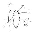
- FIG. 1illustrates a polarization-modulating optical element 1 of an optically active material.
- optically active crystalswith at least one optical crystal axis which are transparent for the wavelength of the light being used.
- TeO 2works in a range of wavelengths from 1000 nm down to 300 nm
- AgGaS 2works from 500 nm to 480 nm
- quartzfrom 800 nm down to 193 nm.
- the polarization-modulating optical element 1is designed so that the element axis is oriented parallel to the optical crystal axis.
- the optical element 1is designed with a thickness profile (measured parallel to the element axis EA) which varies in the directions perpendicular to the element axis EA, also comprising variations in thickness of the optical element in an azimuth direction ⁇ (see FIG. 3 ) at e.g. a fixed distance of the element axis EA.
- FIG. 2will serve to explain the function of optically active crystals, and in particular of polarization-modulating elements made from such crystals, in more detail.
- Optically active crystalshave at least one optical axis OA which is inherent in the crystal structure.
- the plane of oscillation of the electrical field vector 206is rotated by an angle ⁇ of proportionate magnitude as the distance d traveled by the light inside the crystal 202 .
- the proportionality factor between distance d and angle of rotationis the specific rotation ⁇ .
- ⁇ (T)is the optical activity coefficient or specific rotation at the temperature T
- ⁇ 0is the specific rotation at a reference temperature T 0 .
- the polarization-modulating optical element 1 of FIG. 1Based on this property of an optically active crystal, it is possible to produce an arbitrarily selected linear polarization distribution by designing the polarization-modulating optical element 1 of FIG. 1 with a thickness profile that varies dependent on the location.
- the thickness profileis designed to have the effect that the directions of polarization of parallel linearly polarized light rays are rotated by an angle that varies dependent on the location where the light ray traverses the optical element.
- the specific rotation ⁇may itself be dependent on the location within the modulating element such that ⁇ becomes an ⁇ (x,y,z) or ⁇ (r, ⁇ ,z), where x,y or r, ⁇ are Cartesian or polar coordinates in a plane perpendicular to the element axis EA (or alternative to the optical axis OA) of the polarization-modulating element, as shown e.g. in FIG. 1 , where z is the axis along the element axis EA.
- x,y or r, ⁇are Cartesian or polar coordinates in a plane perpendicular to the element axis EA (or alternative to the optical axis OA) of the polarization-modulating element, as shown e.g. in FIG. 1 , where z is the axis along the element axis EA.
- r, ⁇ , ⁇ , or othersis possible.
- Doptical effective thickness
- ⁇may also depend on the z-direction (along the optical axis or element axis EA, or more general along a preferred direction in an optical system or a direction parallel to the optical axis of an optical system)
- the optical effective thickness Dis calculated by integrating the specific rotation ⁇ along the light path of a light ray within the polarization-modulating optical element.
- the present inventionrelates to an optical system comprising an optical axis or a preferred direction given by the direction of a light beam propagating through the optical system.
- the optical systemalso comprises a polarization-modulating optical element described by coordinates of a coordinate system, wherein one preferred coordinate of the coordinate system is parallel to the optical axis of the optical system or parallel to the preferred direction.
- the polarization-modulating optical elementcomprises optical active material and also a profile of effective optical thickness D as defined above, wherein the effective optical thickness D varies at least as a function of one coordinate different from the preferred coordinate of the coordinate system describing the polarization-modulating optical element.
- the effective optical thickness Dvaries at least as a function of the x- or y-coordinate, different from the z-coordinate (the preferred coordinate).
- FIG. 3illustrates an embodiment of the polarization-modulating optical element 301 which is suited specifically for producing a tangential polarization.
- a detailed descriptionwill be presented in the context of FIGS. 4 d and 5 .
- the embodiment illustrated in FIG. 3will serve to introduce several technical terms that will be used hereinafter with the specific meanings defined here.
- the polarization-modulating optical element 301has a cylindrical shape with a base surface 303 and an opposite surface 305 .
- the base surface 303is designed as a planar circular surface.
- the element axis EAextends perpendicular to the planar surface.
- the opposite surface 305has a contour shape in relation to the element axis EA in accordance with a given thickness profile.
- the optical axis of the optically active crystalruns parallel to the element axis EA.
- the reference axis RAwhich extends in the base plane, intersects the element axis at a right angle and serves as the reference from which the azimuth angle ⁇ is measured. In the special configuration illustrated in FIG.
- the thickness of the polarization-modulating optical element 301is constant along a radius R that is perpendicular to the element axis EA and directed at an angle ⁇ relative to the reference axis RA.
- the optical element 301has an optional central bore 307 coaxial with the element axis EA.
- the polarization-modulating optical element 301not necessary need to comprise a planar base surface 303 .
- This surfacein general can also comprise a contour shaped surface e.g. similar or equal to the surface as designated by 305 shown in FIG. 3 . In such a case it is of advantage to describe the contour surfaces 303 and 305 relative to a plane surface perpendicular to the optical axis or element axis.
- FIG. 4 aschematically illustrates a further embodiment of the polarization-modulating optical element 401 .
- the element axis EA through the center of the polarization-modulating optical element 401 in this representationruns perpendicular to the plane of the drawing, and the optical crystal axis of the crystal runs parallel to the element axis.
- the polarization-modulating optical element 401has an optional central bore 407 .
- the polarization-modulating optical element 401is divided into a large number of planar-parallel portions 409 in the shape of sectors of a circle which differ in their respective thicknesses. Alternative embodiments with different shapes of the portions 409 are conceivable. They could be configured, e.g., as hexagonal, square, rectangular or trapeze-shaped raster elements.
- the embodiment according to FIG. 4 acan be modified such that the different thicknesses of the sectors should be understood as different effective optical thicknesses D.
- the specific rotation ⁇may vary from one segment to the other too.
- the polarization-modulating optical elementcan e.g. have a shape as shown in FIG. 4 a in which the sectors 409 are at least partly exchanged e.g. by any optical inactive material, which is the simplest case to vary the specific rotation ⁇ to zero.
- the sectors 409may be replaced by cuvettes or cells which are filed with an optical active or optical inactive liquid.
- the polarization-modulating optical elementmay comprise optical active and optical inactive sections.
- Such an optical system according to the present inventionmay comprise a polarization-modulating optical element which comprises an optically active or an optically inactive liquid and/or an optically active crystal. Further, it is advantageously possible that the polarization-modulating optical element of the optical system according to the present invention comprises clockwise and counterclockwise optically active materials. These materials could be solid or liquid optically active materials.
- the formation of a certain temperature distribution within the liquidmay be possible with appropriate heating and/or cooling means controlled by control means.
- the optical systems in accordance with the present inventionadvantageously modify respective planes of oscillation of a first linearly polarized light ray and a second linearly polarized light ray. Both light rays propagating through the optical system, and being at least a part of the light beam propagating through the optical system.
- the light raysare also passing the polarization-modulating optical element with different paths, and are rotated by a respective first and second angle of rotation such that the first angle is different of the second angle.
- the polarization-modulating optical element of the optical systems according to the present inventiontransform a light bundle with a first linear polarization distribution, which enters said polarization-modulating optical element, into a light bundle exiting said polarization-modulating optical element.
- the exiting light bundlehaving a second linear polarization distribution, wherein the second linear polarization distribution is different from the first linear polarization distribution.
- the term azimuthal section as used in the present contextmeans a section traversing the thickness profile d( ⁇ ,r) along the circle 411 marked in FIG. 4 a , i.e., extending over an azimuth angle range of 0° ⁇ 360° at a constant radius r.
- An azimuthal section of a polarization-modulating optical element 401 that is divided into sector-shaped portionshas a stair-shaped profile in which each step corresponds to the difference in thickness d or optical effective thickness D between neighboring sector elements.
- the profilehas e.g. a maximum thickness d max and a minimum thickness d min .
- d maxmaximum thickness
- d minminimum thickness
- the height of each individual step of the profiledepends on the number n of sector elements and has a magnitude of 360°/(n ⁇ ).
- the profilehas a discontinuity where the thickness of the polarization-modulating optical element 401 jumps from d min to d max .
- the profilehas e.g. a maximum optical effective thickness D max and a minimum optical effective thickness D min , and the geometrical thickness d is e.g. constant, resulting in a variation of the specific rotation ⁇ of the individual segments 409 of the element 401 .
- the geometrical thickness dis e.g. constant, resulting in a variation of the specific rotation ⁇ of the individual segments 409 of the element 401 .
- the change of the specific rotation of each individual step of the profiledepends on the number n of sector elements 409 and has a magnitude of 360°/(n ⁇ d).
- the individual sector elements 409are preferably made of or comprises cuvettes or cells, filled with an optical active liquid with the required specific rotation ⁇ .
- the required specific rotatione.g. can be adjusted by the concentration of the optical active material of the liquid, or by changing the liquid material itself.
- the segments 409 of a polarization-modulating optical element 401may comprise components of solid optically active material (like crystalline quartz) and cells or cuvettes filled with optically active material, and these components are placed behind each other in the light propagation direction.
- the cuvette itselfmay comprise optically active material like crystalline quartz.
- the polarization-modulating optical element of the foregoing descriptionconverts linearly polarized incident light into a linear polarization distribution in which the oscillation planes of linearly polarized light rays are rotated by an angle that depends on the thickness (or optical effective thickness) of each individual sector element.
- the angle by which the direction of polarization is rotatedis constant over an individual sector element.
- the distribution function for the directions of the oscillation planes of the individual field vectorstakes only certain discrete values.
- a continuous distribution of linear polarizationscan be achieved with an optical element that has a continuously varying thickness (optical effective thickness) profile along an azimuthal section.
- FIG. 4 cAn example of a continuously varying thickness profile is illustrated in FIG. 4 c .
- the slopeis defined a slope of a screw.
- the slopedepends on the distance of the element axis, e.g. if the polarization-modulating optical element 301 has a given constant screw-slope (lead of a screw).
- a further embodiment of a polarization-modulating optical element which is shown in FIG. 4 dhas a thickness profile (in general optical effective thickness profile) which is likewise suitable for producing a continuous distribution of linear polarizations, in particular a tangentially oriented polarization.
- This thickness profilecorresponds to the embodiment shown in FIG. 3 , in which the angle ⁇ is measured in counterclockwise direction.
- FIG. 4 erepresents the thickness profile (in general optical effective thickness profile) along an azimuthal section for a further embodiment of the polarization-modulating optical element 401 .
- the azimuthal sectionis in this case a linear function of the azimuth angle ⁇ with a first slope m for 0 ⁇ 180° and with a second slope n for 180° ⁇ 360°.
- the slopes m and nare of equal absolute magnitude but have opposite signs.
- FIG. 4 fschematically illustrates a further embodiment 421 of the polarization-modulating optical element.
- the element axis EA through the center of the polarization-modulating optical element 421runs perpendicular to the plane of the drawing, and the optical crystal axis runs parallel to the element axis.
- the polarization-modulating optical element 421comprises of four separate sector-shaped parts 422 , 423 , 424 , 425 of an optically active crystal material which are held together by a mounting device 426 which can be made, e.g., of metal and whose shape can be described as a circular plate 427 with four radial spokes 428 .
- the mountingis preferably opaque to the radiation which is entering the polarization-modulating optical element, thereby serving also as a spacer which separates the sector-shaped parts 422 , 423 , 424 , 425 from each other.
- FIG. 4 fis not intended to be limited to any specific shape and area of mounting device 426 , which may also be omitted.
- incident light which is entering the polarization-modulating optical elementcan also be selectively directed onto the sector-shaped parts, e.g. by means of a diffractive structure or other suitable optical components.
- the sector-shaped parts 422 and 424have a first thickness d 1 which is selected so that the parts 422 and 424 cause the plane of oscillation of linearly polarized axis-parallel light to be rotated by 90°+p ⁇ 180°, where p represents an integer.
- the sector-shaped parts 423 and 425have a second thickness d 2 which is selected so that the parts 423 and 425 cause the plane of oscillation of linearly polarized axis-parallel light to be rotated by q ⁇ 180°, where q represents an integer other than zero.
- the exiting lighthas a polarization distribution which is exactly tangential at the centerlines 429 and 430 of the sector-shaped parts 422 , 423 , 424 , 425 and which approximates a tangential polarization distribution for the rest of the polarization-modulating optical element 421 .
- the exiting lighthas a polarization distribution which is exactly radial at the centerlines 429 and 430 of the sector-shaped parts 422 , 423 , 424 , 425 and which approximates a radial polarization distribution for the rest of the polarization-modulating optical element 421 .
- FIG. 4 fis not intended to be limited to the shapes and areas and the number of sector-shaped parts exemplarily illustrated in FIG. 4 f , so that other suitable shapes (having for example but not limited to trapeze-shaped, rectangular, square, hexagonal or circular geometries) as well as more or less sector-shaped parts 422 , 423 , 424 and 425 can be used.
- the angles of rotation ⁇ 1 and ⁇ 2 provided by the sector-shaped parts 422 , 423 , 424 , 425i.e.
- the corresponding thicknesses of the sector-shaped parts 422 , 423 , 424 , 425 )may be more generally selected to approximately conform to the expression
- (2n+1) ⁇ 90°, with n representing an integer, for example to consider also relative arrangements where incoming light is used having a polarization plane which is not necessarily aligned with the x- or y-direction.
- nrepresenting an integer
- a polarization-modulating optical element of crystalline quartzwith the design according to FIGS. 3 and 4 d .
- the specific rotation ⁇ of quartz for light with a wavelength of 193 nmis in the range of (325.2 ⁇ 0.5)°/mm, which was measured at a wavelength of 180 nm, or more precise it is 321.1°/mm at 21.6° C.
- the strength and effect of the optical activityis approximately constant within a small range of angles of incidence up to 100 mrad.
- An embodimentcould for example be designed according to the following description: An amount of 276.75 ⁇ m, which approximately equals 90°/ ⁇ , is selected for the minimum thickness d min , if crystalline quartz is used Alternatively, the minimum thickness d min can also be an integer multiple of this amount.
- the element diameteris 110 mm, with the diameter of the optically active part being somewhat smaller, for example 105 mm.
- the base surfaceis designed as a planar surface as illustrated in FIG. 3 .
- the opposite surfacehas a thickness profile d(r, ⁇ ) in accordance with FIG. 4 d .
- the thickness profileis defined by the following mathematical relationships:
- the polarization-modulating optical element according to this embodimenthas a central opening 407 with a diameter 10.5, i.e., one-tenth of the maximum aperture.
- the thickness maxima and minima, which are found at the discontinuities,are 830.26 ⁇ m and 276.75 ⁇ m, respectively for the first given example.
- the embodiment of the foregoing descriptioncan be produced with a robot-polishing process. It is particularly advantageous to produce the polarization-modulating element from two wedge-shaped or helically shaped half-plates which are seamlessly joined together after polishing. If the element is produced by half-plates, it is easy and in some applications of additional advantage to use one clockwise and one counterclockwise optically active material like clockwise crystalline and counterclockwise crystalline quartz (R-quartz and L-quartz).
- FIG. 5schematically illustrates how a polarization-modulating optical element 501 with a thickness profile according to FIGS. 3 and 4 d converts the polarization distribution of an entering light bundle 513 with a uniformly oriented linear polarization distribution 517 into a tangential polarization 519 of an exiting light bundle 515 .
- FIG. 6schematically illustrates how an optical arrangement with a polarization-modulating optical element 601 with a thickness profile according to FIGS. 3 and 4 d in combination with a further polarization-modulating element 621 converts the polarization distribution of an entering light bundle 613 with a uniformly oriented linear polarization distribution 617 into a radial polarization 623 of an exiting light bundle 615 .
- the polarization-modulating optical element 601produces a tangential polarization distribution.
- a tangential polarization distributioncan be converted into a radial polarization distribution by a 90°-rotation of the respective oscillation plane of each individual linearly polarized ray of the light bundle.
- FIG. 6There are several different possibilities to accomplish this with an optical arrangement according to FIG. 6 .
- One possible conceptis to arrange a planar-parallel plate of an optically active crystal as a further polarization-modulating element 621 in the light path, where the thickness of the plate is approximately 90°/ ⁇ p with ⁇ p representing the specific rotation of the optically active crystal.
- the optical crystal axis of the planar parallel plateruns likewise parallel to the element axis.
- the further polarization-modulating element 621can be configured as a 90°-rotator that is assembled from two half-wave plates.
- a 90°-rotatorconsists of two half-wave plates of birefringent crystal material.
- Each platehas a slow axis associated with the direction of the higher refractive index and, perpendicular to the slow axis, a fast axis associated with the direction of the lower refractive index.
- the two half-wave platesare rotated relative to each other so their respective fast and slow axes are set at an angle of 45° from each other.
- the further polarization-modulating optical element 621can be connected to the polarization-modulating optical element 601 .
- an exchange devicethat allows the further polarization-modulating element 621 to be placed in the light path and to be removed again or to be replaced by another element.
- a tangential polarization distributioncan also be produced with a polarization-modulating optical element that has a thickness profile in accordance with FIG. 4 e .
- the thickness profile in this embodiment of the inventionhas no discontinuities.
- the uniformly oriented polarization distribution 717 of the entering light bundle 713is first transformed by the polarization-modulating optical element 701 into a linear polarization distribution 727 of an exiting light bundle 715 .
- the one-half of the entering light bundle 713 that passes through the polarization-modulating optical element 701 in the azimuth range 0 ⁇ 180° of the thickness profile shown in FIG. 4 eis converted so that the corresponding one-half of the exiting light bundle has a tangential polarization distribution.
- the other halfhas a different, non-tangential polarization distribution 727 .
- a further polarization-modulating optical elementis needed in the light path in order to completely convert the polarization distribution 727 of the light bundle 715 exiting from the polarization-modulating optical element 701 into a tangential polarization distribution 719 .
- the further polarization-modulating optical elementis in this case configured as a planar-parallel plate 725 with a first half 729 and a second half 731 .
- a plan view of the planar-parallel plate 725is shown in FIG. 7 b .
- the first half 729is made of an isotropic material that has no effect on the state of polarization of a light ray, while the second half 731 is designed as a half-wave plate.
- the planar-parallel plate 725 in the optical arrangement of FIG. 7 ais oriented so that a projection RA′ of the reference axis RA of the polarization-modulating optical element 701 onto the planar-parallel plate runs substantially along the separation line between the first half 729 and the second half 731 .
- the slow axis LA of the birefringence of the half-wave plateis perpendicular to this separation line.
- tangential polarizationcan also be achieved with a polarization-modulating optical element, having a thickness profile as given by FIG.
- each wedge-shaped elementhas a constant screw-slope, but the slopes have different directions as shown in the profile of FIG. 4 e .
- the slopes of the geometrical thickness dhave the same absolute values, it is sufficient if the slopes D of the optical effective thicknesses have the same absolute values.
- the specific rotations ⁇are different regarding absolute values for the two wedge-shaped elements which form the polarization-modulating optical element.
- FIG. 8schematically illustrates a microlithography projection system 833 which includes the light source unit 835 , the illumination system 839 , the mask 853 which carries a microstructure, the projection objective 855 , and the substrate 859 that is being exposed to the projection.
- the light source unit 835includes a DUV- or VUV-laser, for example an ArF laser for 192 nm, an F 2 laser for 157 nm, an Ar 2 laser for 126 nm or a Ne 2 laser for 109 nm, and a beam-shaping optical system which produces a parallel light bundle.
- the rays of the light bundlehave a linear polarization distribution where the oscillation planes of the electrical field vectors of the individual light rays are oriented in a uniform direction.
- the principal configuration of the illumination system 839is described in DE 195 29 563 (U.S. Pat. No. 6,258,433).
- the parallel light bundlefalls on the divergence-increasing optical element 837 .
- a divergence-increasing optical elementone could use for example a raster plate with an arrangement of diffractive or refractive raster elements. Each raster element generates a light bundle whose angle distribution is determined by the dimension and focal length of the raster element.
- the raster plateis located in or near the object plane of an objective 840 that follows downstream in the light path.
- the objective 840is a zoom objective which generates a parallel light bundle with a variable diameter.
- a direction-changing mirror 841directs the parallel light bundle to an optical unit 842 which contains an axicon (i.e., a rotationally symmetric prism arrangement) 843 .
- the zoom objective 840in cooperation with the axicon 843 generates different illumination profiles in the pupil plane 845 , depending on the setting of the zoom and the position of the axicon elements.
- a polarization-modulating optical element 801is arranged in the pupil plane 845 .
- the polarization-modulating optical element 801is followed in the light path by a compensation plate 847 which has a thickness profile designed to compensate the angle deviations which the polarization-modulating optical element causes in the light rays that pass through it.
- the optical unit 842is followed by a reticle-masking system (REMA) 849 .
- the REMA Objective 851projects an image of the reticle-masking system 849 onto the structure-carrying mask (reticle) 853 , whereby the illuminated area of the reticle 853 is delimited.
- the projection objective 855projects the image of the structure-carrying mask 853 onto the light-sensitive substrate 859 .
- the space between the last optical element 857 of the projection objective and the light-sensitive substrate 859contains an immersion liquid 861 with a refractive index different from air.
- An additional advantage of the present inventionis that polarization-modulating optical elements or the optical system according to the present invention can be used for adjusting the polarization distribution and also for temperature compensation of the polarization distribution in a microlithography projection system as described in FIG. 8 .
- Advanced microlithography projection systemsrequire in some applications a predefined polarization distribution at the reticle 853 with an accuracy of about 5° or even better, in some cases even better than 1°.
- the optical systempreferably comprises a polarization control system for controlling the polarization distribution of the light beam which is propagating through the optical system.
- the polarization distribution of interestis at a predefined location in the optical system.
- the polarization control systemcomprises at least one heating or cooling device to modify the temperature and/or the temperature distribution of the polarization-modulating optical element to affect the polarization distribution of the light beam at the predefined location.
- the polarization-modulating optical elementmay have a varying or constant effective optical thickness.
- the optical systemcomprises an optical axis or a preferred direction given by the direction of a light beam propagating through the optical system.
- the optical systemadditionally comprises a polarization-modulating optical element described by coordinates of a coordinate system, wherein one preferred coordinate of the coordinate system is parallel to the optical axis or parallel to said preferred direction.
- the polarization-modulating optical elementcomprises solid and/or liquid optically active material, wherein the effective optical thickness is constant as a function of at least one coordinate different from the preferred coordinate of the coordinate system.
- the optical systemcomprises further a polarization control system for controlling the polarization distribution of the light beam (propagating through the optical system) at a predefined location in the optical system, and the polarization control system comprises at least one heating or cooling device to modify the temperature and/or the temperature distribution of the polarization-modulating optical element to affect the polarization distribution of the light beam at the predefined location.
- the optical axis OA of the parallel plate 901is directed parallel or approximately parallel to the propagation of the light (indicated by reference numeral 950 ) in the optical system.
- Approximately parallelmeans that the angle between the optical axis OA of the parallel plate 901 and the direction of the light propagating through the optical system is smaller than 200 mrad, preferably smaller than 100 mrad or even smaller than 50 mrad.
- Controlling the temperature of the plate 901will result in a controlled change of polarization. If for example the temperature of the plate will be controlled in a range of about 20° C. to 40° C., the polarization angles can be controllably changed in a range of about ⁇ 13.5° for such a plate 901 made of quartz.
- the synthetic quartzFor a 90° rotation of the polarization plane the synthetic quartz should be at least 278.5 ⁇ m thick and for 180° at least 557.1 ⁇ m, for 270° the thickness should be 835.5 ⁇ m and for a 360° rotation of the polarization the thickness is 1.114 mm.
- the manufacturing tolerances regarding thicknessare about ⁇ 2 ⁇ m. Thus the manufacturing tolerance results in an inaccuracy of the angle of the polarization plane of the light which passes the plate of about ⁇ 0.64° at about 21.6° C. and 193 nm.
- the temperature control of the plate 901can be done by closed-loop or open-loop control, using a temperature sensing device with at least one temperature sensor 902 , 903 for determining the temperature of the plate 901 (or providing a temperature sensor value which is representative or equal to the temperature and/or the temperature distribution of the polarization-modulating optical element), at least a heater 904 , 905 , preferably comprising an infrared heater, for heating the plate by infrared radiation 906 , and a control circuit 910 for controlling the at least one heater 904 , 905 .
- a infrared sensitive CCD-element with a projection opticsmay be used, wherein the projection optics images at least a part of the plate 901 onto the CCD-element such that a temperature profile of the viewed part of the plate 901 can be determined by the analysis of the CCD-element signals.
- the control circuit 910may comprise a computer system 915 or may be connected to the computer or control system 915 of the microlithography projection system 833 (see FIG. 8 ).
- the heater or heating system(and also any cooling device like a Peltier element) is arranged such that it is not in the optical path of the microlithography projection system 833 , or that it is not in the optical path of the light beam which is propagating through the optical system according to an embodiment of the present invention.
- the optical system with the polarization control system according to the present inventionis used in a system with at least one additional optical element arranged between the polarization-modulating optical element and the predefined location in the optical system such that the light beam contacts the at least one additional optical element when propagating from the polarization-modulating optical element to the predefined location.
- the additional optical elementpreferably comprises a lens, a prism, a mirror, a refractive or a diffractive optical element or an optical element comprising linear birefringent material.
- the optical system according to the present inventionmay form a part of a microlithography projection system 833 .
- the temperature of the polarization-manipulating optical element 901corresponds to a predefined temperature profile.
- a temperature profileis achieved by using a plurality of infrared heaters 904 , 905 to produce a radiation distribution across the optical element 901 which heats the optical element 901 in a controlled way with a control circuit as already described.
- a plurality of temperature sensors 902 , 903can be used for the control circuit 910 .
- the polarization state in a field plane or pupil plane of the microlithography projection system 833can be adjusted locally.
- the heater or heating elements 904 , 905may be replaced or supplemented by one or more Peltier-elements 907 , 908 .
- the Peltier-element or elementsare preferably connected to the control circuit 910 such that a control by open and/or closed loop control is possible.
- the advantage of the Peltier-elementsis that also a controlled cooling of the polarization-manipulating optical element 901 can be achieved. Heating and cooling the optical element 901 at the same time result in complex temperature distributions in the polarization-modulating optical element 901 , which result in complex polarization distributions of the light 950 propagating e.g. through the microlithography projection system 833 , after passing the element 901 .
- other heating and cooling meansthan the ones mentioned above can be used to achieve a required temperature profile or a required temperature of the polarization-modulating optical element 901 .
- the application of the plane plate 901 as polarization-modulating optical element 801 in the illumination system of a microlithography projection apparatus 833is preferably in the pupil plane 845 and/or at positions between the light source unit 835 and the mentioned pupil plane 845 . Applying the plane plate 901 at these locations has the advantage that the angle of incidence of the light which passes through the plate 901 and also passing through the microlithography projection apparatus is smaller than about 6° (100 mrad).
- the state of the polarization of the light passed through the polarization-modulating element 901 or the optical system according to the present inventionis measured.
- the polarization control systemcomprises a polarization measuring device providing a polarization value representative for or equal to the polarization or the polarization distribution of the light beam at the predetermined location in the optical system.
- the control circuitcontrols the at least one heating or cooling device dependent on the temperature sensor value and/or the polarization value by open or closed loop control.
- the measured state of polarizationis compared with a required state and in the case that the measured state deviates more than a tolerable value, the temperature and/or the temperature distribution of the polarizing-modulating element like the plane plate 901 is changed such that the difference between the measured and the required state of polarization becomes smaller, and if possible such small that the difference is within a tolerable value.
- the measurement of the state of polarizationis measured in-situ or with a separate special measurement, depending on the polarization measuring device 960 .
- the polarization measuring devicemay be connected with the control circuit 910 , such that depending on the measured polarization state values the heating means 904 , 905 and/or 907 , 908 are controlled heated and/or cooled such that the measured and the required state of polarization becomes smaller.
- the controlcan be done in open or closed loop modus.
- the plane plate 901 used as polarization-modulating optical element or being a part of such elementis especially appropriate to correct orientations of polarization states of the passed light bundles.
- the plane plate 901(comprising or consisting of optically active material), used as a polarization-modulating optical element, is combined with a plate 971 (see FIG. 10 ), comprising or consisting of linear birefringent material.
- a plate 971(see FIG. 10 ), comprising or consisting of linear birefringent material.
- the orientation and the phase of the passing light bundle 950can be subjected such that e.g. a plane polarized light bundle becomes elliptically polarized after passing both plane plates 901 and 971 , or vice versa.
- at least one plate 901 or 971is controlled regarding its temperature and/or temperature distribution as described in connection with FIG. 9 .
- the sequence of the plates 901 and 971may be changed such that the passing light bundles are first passing through the plate 971 , comprising or consisting of linear birefringent material, and than through the plate 901 , comprising or consisting of optical active material, or vice versa.
- both platesare consecutively arranged along the optical axis OA of the system.
- more than one plate comprising or consisting of linear birefringent material, and/or more than one plate comprising or consisting of optical active materialmay be used to manipulate the state of polarization of the passing light bundles.
- a plane plate 971 , or 901may be exchanged by a liquid cell or cuvette containing optically active material.
- plane plates 971comprising or consisting of linear birefringent material
- plate 901comprising or consisting of optical active material
- This element 981can be for example a lens, a diffractive or refractive optical element, a mirror or an additional plane plate.
- the temperature compensationmakes use of the realization that for synthetic quartz there exist one quartz material with a clockwise and one quartz material with a counterclockwise optical activity (R-quartz and L-quartz). Both, the clockwise and the counterclockwise optical activities are almost equal in magnitude regarding the respective specific rotations ⁇ . The difference of the specific rotations is less than 0.3%. Whether the synthetic quartz has clockwise (R-quartz) or counterclockwise (L-quartz) optical activity dependents on the seed-crystal which is used in the manufacturing process of the synthetic quartz.
- R- and L-quartzcan be combined for producing a thermal or temperature compensated polarization-modulating optical element 911 as shown in FIG. 11 .
- a temperature compensated polarization-modulating optical element 911is equivalent to a plane plate of synthetic quartz of thickness d.
- two plane plates 921 and 931are arranged behind each other in the direction 950 of the light which is propagating through the optical system which comprises the temperature compensated polarization-modulating optical element 911 .
- the arrangement of the platesis such that one plate 931 is made of R-quartz with thickness d R , and the other 921 is made of L-quartz with thickness d L , and
- d.
- d L557.1 ⁇ m+287.5 ⁇ m
- any structured polarization-modulating optical element made of R- or L-quartzlike e.g. the elements as described in connection with FIGS. 3 and 4 a can be combined with a plane plate of the respective other quartz type (L- or R-quartz) such that the combined system 911 will have a reduced temperature dependence regarding the change of the polarization.
- a structured optical element made of the respective other quartz typemay be used such that in FIG. 11 the shown plates 921 and 931 can be structured polarization-modulating optical elements as mentioned in this specification, having specific rotations of opposite signs, changing the state of polarization clockwise and counterclockwise.
- the present inventionalso relates to an optical system comprising an optical axis OA or a preferred direction 950 given by the direction of a light beam propagating through the optical system.
- the optical systemcomprising a temperature compensated polarization-modulating optical element 911 described by coordinates of a coordinate system, wherein one preferred coordinate of the coordinate system is parallel to the optical axis OA or parallel to said preferred direction 950 .
- the temperature compensated polarization-modulating optical element 911comprises a first 921 and a second 931 polarization-modulating optical element.
- the first and/or the second polarization-modulating optical elementcomprising solid and/or liquid optically active material and a profile of effective optical thickness, wherein the effective optical thickness varies at least as a function of one coordinate different from the preferred coordinate of the coordinate system.
- the first 921 and/or the second 931 polarization-modulating optical elementcomprises solid and/or liquid optically active material, wherein the effective optical thickness is constant as a function of at least one coordinate different from the preferred coordinate of the coordinate system.
- first and the second polarization-modulating optical elements 921 , 931comprise optically active materials with specific rotations of opposite signs, or the first polarization-modulating optical element comprises optically active material with a specific rotation of opposite sign compared to the optically active material of the second polarization-modulating optical element.
- the absolute value of the difference of the first and the second thickness of the first and second plateis smaller than the thickness of the smaller plate.
- a polarization-modulating elementcomprises an optically active and/or optically inactive material component subjected to a magnetic field such that there is a field component of the magnetic field along the direction of the propagation of the light beam through the polarization-modulating element.
- the optical active material componentmay be construed as described above. However, also optical inactive materials can be used, having the same or similar structures as described in connection with the optical active materials. The application of a magnetic field will also change the polarization state of the light passing through the optical active and/or optical inactive material due to the Faraday-effect, and the polarization state can be controlled by the magnetic field.
- polarization-modulating optical elementor for the optical systems according to the present invention are described in this application. Further, also additional embodiments of polarization-modulating optical elements or optical systems according to the present invention may be obtained by exchanging and/or combining individual features and/or characteristics of the individual embodiments described in the present application.
Landscapes
- Physics & Mathematics (AREA)
- General Physics & Mathematics (AREA)
- Optics & Photonics (AREA)
- Nonlinear Science (AREA)
- Polarising Elements (AREA)
- Exposure Of Semiconductors, Excluding Electron Or Ion Beam Exposure (AREA)
- Exposure And Positioning Against Photoresist Photosensitive Materials (AREA)
Abstract
Description
- The invention relates to an optical element that affects the polarization of light rays. The optical element has a thickness profile and consists or comprises of an optically active crystal with an optical axis.
- In the continuing effort to achieve structures of finer resolution in the field of microlithography, there is a parallel pursuit of substantially three guiding concepts. The first of these is to provide projection objectives of very high numerical aperture. Second is the constant trend towards shorter wavelengths, for example 248 nm, 193 nm, or 157 nm. Finally, there is the concept of increasing the achievable resolution by introducing an immersion medium of a high refractive index into the space between the last optical element of the projection objective and the light-sensitive substrate. The latter technique is referred to as immersion lithography.
- In an optical system that is illuminated with light of a defined polarization, the s- and p-component of the electrical field vector, in accordance with Fresnel's equations, are subject to respectively different degrees of reflection and refraction at the interface of two media with different refractive indices. In this context and hereinafter, the polarization component that oscillates parallel to the plane of incidence of a light ray is referred to as p-component, while the polarization component that oscillates perpendicular to the plane of incidence of a light ray is referred to as s-component. The different degrees of reflection and refraction that occur in the s-component in comparison to the p-component have a significant detrimental effect on the imaging process.
- This problem can be avoided with a special distribution of the polarization where the planes of oscillation of the electrical field vectors of individual linearly polarized light rays in a pupil plane of the optical system have an approximately radial orientation relative to the optical axis. A polarization distribution of this kind will hereinafter be referred to as radial polarization. If a bundle of light rays that are radially polarized in accordance with the foregoing definition meets an interface between two media of different refractive indices in a field plane of an objective, only the p-component of the electrical field vector will be present, so that the aforementioned detrimental effect on the imaging quality is reduced considerably.
- In analogy to the foregoing concept, one could also choose a polarization distribution where the planes of oscillation of the electrical field vectors of individual linearly polarized light rays in a pupil plane of the system have an orientation that is perpendicular to the radius originating from the optical axis. A polarization distribution of this type will hereinafter be referred to as tangential polarization. If a bundle of light rays that are tangentially polarized in accordance with this definition meets an interface between two media of different refractive indices, only the s-component of the electrical field vector will be present so that, as in the preceding case, there will be uniformity in the reflection and refraction occurring in a field plane.
- Providing an illumination with either tangential or radial polarization in a pupil plane is of high importance in particular when putting the aforementioned concept of immersion lithography into practice, because of the considerable negative effects on the state of polarization that are to be expected based on the differences in the refractive index and the strongly oblique angles of incidence at the respective interfaces from the last optical element of the projection objective to the immersion medium and from the immersion medium to the coated light-sensitive substrate.
- U.S. Pat. No. 6,191,880 B1 discloses an optical arrangement for generating an approximately radial polarization. The arrangement includes among other things a raster of half-wave plates whose respective directions of preference are oriented so that when linearly polarized light passes through the raster arrangement, the plane of oscillation is rotated into the direction of a radius originating from the optical axis. However, because the raster arrangement is produced by joining a large number of individually oriented half-wave plates, it is expensive to produce. Furthermore, the change in the direction of the polarization is constant within the area of each individual half-wave plate whose diameter is typically between 10 and 20 mm, so that no continuous radial polarization can be produced through this concept.
- A birefringent element of crystalline quartz with an irregularly varying thickness is proposed in DE 198 07 120 A1 for the compensation of local aberrations of a defined state of polarization in an optical system. However, the variation in thickness in a birefringent element of this type leads to locally different states of polarization. In particular, the linear state of polarization is, as a rule, not preserved in an arrangement of this type.
- The present invention therefore has the objective to propose a polarization-modulating optical element which—with a minimum loss of intensity—affects the polarization of light rays in such a way that from linearly polarized light with a first distribution of the directions of the oscillation planes of individual light rays, the optical element generates linearly polarized light with a second distribution of the directions of the oscillation planes of individual light rays.
- Further objects of the present invention are to propose an optical system with improved properties of the polarization-modulating optical element regarding thermal stability of the second distribution of oscillation planes (polarization distribution), and to minimize the influence of additional optical elements in the optical system to the polarization distribution after the light rays have passed these elements.
- To meet the foregoing objectives, a polarization-modulating optical element is proposed which consists or comprises of an optically active crystal and which, according to the invention, is shaped with a thickness profile that varies in the directions perpendicular to the optical axis. Further, the optical systems as described in claims57,64,65,70 and75 meet the objects of the present invention. Additional preferred embodiments of the optical systems according to the present invention are given in the dependent claims.
- A polarization-modulating optical element according to the invention has the effect that the plane of oscillation of a first linearly polarized light ray and the plane of oscillation of a second linearly polarized light ray are rotated, respectively, by a first and a second angle of rotation, with the first angle of rotation being different from the second angle of rotation. According to the invention, the polarization-modulating optical element is made of an optically active material.
- Advantageous further developments of the inventive concept are described hereinafter.
- In order to generate from linearly polarized light an arbitrarily selected distribution of linearly polarized light rays with a minimum loss of intensity, an optically active crystal with an optical axis is used as raw material for the polarization-modulating optical element. The optical axis of a crystal, also referred to as axis of isotropy, is defined by the property that there is only one velocity of light propagation associated with the direction of the optical axis. In other words, a light ray traveling in the direction of an optical axis is not subject to a linear birefringence. The polarization-modulating optical element has a thickness profile that varies in the directions perpendicular to the optical axis of the crystal. The term “linear polarization distribution” in this context and hereinafter is used with the meaning of a polarization distribution in which the individual light rays are linearly polarized but the oscillation planes of the individual electrical field vectors can be oriented in different directions.
- If linearly polarized light traverses the polarization-modulating optical element along the optical axis of the crystal, the oscillation plane of the electrical field vector is rotated by an angle that is proportional to the distance traveled inside the crystal. The sense of rotation, i.e., whether the oscillation plane is rotated clockwise or counterclockwise, depends on the crystal material, for example right-handed quartz vs. left-handed quartz. The polarization plane is parallel to the respective directions of the polarization and the propagation of the light ray. In order to produce an arbitrarily selected distribution of the angles of rotation, it is advantageous if the thickness profile is designed so that the plane of oscillation of a first linearly polarized light ray and the plane of oscillation of a second linearly polarized light ray are rotated, respectively, by a first and a second angle of rotation, with the first angle of rotation being different from the second angle of rotation. By shaping the element with a specific thickness at each location, it is possible to realize arbitrarily selected angles of rotation for the oscillation planes.
- Different optically active materials have been found suitable dependent on the wavelength of the radiation being used, specifically quartz, TeO2, and AgGaS2.
- In an advantageous embodiment of the invention, the polarization-modulating optical element has an element axis oriented in the same direction as the optical axis of the crystal. In relation to the element axis, the thickness profile of the optical element is a function of the azimuth angle θ alone, with the azimuth angle θ being measured relative to a reference axis that intersects the element axis at a right angle. With a thickness profile according to this design, the thickness of the optical element is constant along a radius that intersects the element axis at a right angle and forms an azimuth angle θ with the reference axis.
- In a further advantageous embodiment of the invention, an azimuthal section d(r=const.,θ) of the thickness profile d(r,θ) at a constant distance r from the element axis is a linear function of the azimuth angle θ. In the ideal case, this azimuthal section has a discontinuity at the azimuth angle θ=0. The linear function d(r=const.,θ) at a constant distance r from the element axis has a slope
- wherein α stands for the specific rotation of the optically active crystal. At the discontinuity location for θ=0, there is an abrupt step in the thickness by an amount of 360°/α. The step at the discontinuity location can also be distributed over an azimuth angle range of a few degrees. However, this has the result of a non-optimized polarization distribution in the transition range.
- In a further advantageous embodiment of the invention, an azimuthal section d(r=const.,θ) of the thickness profile d(r,θ) at a constant distance r from the element axis is a linear function of the azimuth angle θ with the same slope m but, in the ideal case, with two discontinuities at the azimuth angles θ=0 and θ=180°, respectively. At each discontinuity location, there is an abrupt step in the thickness by an amount of 180°/α. The two abrupt steps at the discontinuity locations can also be distributed over an azimuth angle range of a few degrees. However, this has the result of a non-optimized polarization distribution in the transition range.
- In a further advantageous embodiment of the invention, an azimuthal section d(r=const.,θ) of the thickness profile d(r,θ) at a constant distance r from the element axis and in a first azimuth angle range of 10°<θ<170° is a linear function of the azimuth angle θ with a first slope m, while in a second azimuth angle range of 190°<θ<350°, the azimuthal section is a linear function of the azimuth angle θ with a second slope n. The slopes m and n have the same absolute magnitude but opposite signs. The magnitude of the slopes m and n at a distance r from the element axis is
- With this arrangement, the thickness profile for all azimuth angles, including θ=0 and θ=180°, is a continuous function without abrupt changes in thickness.
- In a further advantageous embodiment of the invention, the polarization-modulating optical element is divided into a large number of planar-parallel portions of different thickness or comprises at least two planar-parallel portions. These portions can for example be configured as sectors of a circle, but they could also have a hexagonal, square, rectangular, or trapezoidal shape.
- In a further advantageous embodiment of the invention, a pair of first plan-parallel portions are arranged on opposite sides of a central element axis of said polarization-modulating optical element, and a pair of second plan-parallel portions are arranged on opposite sides of said element axis and circumferentially displaced around said element axis with respect to said first plan-parallel portions, wherein each of said first portions has a thickness being different from a thickness of each of said second portions.
- In a further advantageous embodiment of the invention, a plane of oscillation of linearly polarized light passing through the polarization-modulating optical element is rotated by a first angle of rotation β1within at least one of said first plan-parallel portions and by a second angle of rotation β2within at least one of said second plan-parallel portions, such that β1and β2are approximately conforming or conform to the expression |β2−β1|=(2n+1)·90°, with n representing an integer.
- In an advantageous embodiment, β1and β2are approximately conforming or conform to the expressions β1=90°+p·180°, with p representing an integer, and β2=q·180°, with q representing an integer other than zero. As will discussed below in more detail, such an embodiment of the polarization modulating optical element may be advantageously used in affecting the polarization of traversing polarized light such that exiting light has a polarization distribution being—depending of the incoming light—either approximately tangentially or approximately radially polarized.
- The pair of second plan-parallel portions may particularly be circumferentially displaced around said element axis with respect to said pair of first plan-parallel portions by approximately 90°.
- In a further advantageous embodiment of the invention, said pair of first plan-parallel portions and said pair of second plan-parallel portions are arranged on opposite sides of a central opening or a central obscuration of said polarization-modulating optical element.
- Adjacent portions of said first and second pairs can be spaced apart from each other by regions being opaque to linearly polarized light entering said polarization-modulating optical element. Said portions of said first and second group can particularly be held together by a mounting. Said mounting can be opaque to linearly polarized light entering said polarization-modulating optical element. The mounting can have a substantially spoke-wheel shape.
- In a further advantageous embodiment of the invention, the polarization-modulating optical element comprises a first group of substantially planar-parallel portions wherein a plane of oscillation of traversing linearly polarized light is rotated by a first angle of rotation β1, and a second group of substantially planar-parallel portions wherein a plane of oscillation of traversing linearly polarized light is rotated by a second angle of rotation, such that β1and β2are approximately conforming or conform to the expression |β2−β1|=(2n+1)·90°, with n representing an integer.
- In a further advantageous embodiment of the invention, β1and β2are approximately conforming to the expressions β1=90°+p·180°, with p representing an integer, and β2=q·180°, with q representing an integer other than zero.
- In a further advantageous embodiment of the invention, the thickness profile of the polarization-modulating optical element has a continuous surface contour without abrupt changes in thickness, whereby an arbitrarily selected polarization distribution can be generated whose thickness profile is represented by a continuous function of the location.
- To ensure an adequate mechanical stability of the optical element, it is important to make the minimal thickness dminof the polarization-modulating optical element at least equal to 0.002 times the element diameter D.
- If the optically active material used for the optical element also has birefringent properties as is the case for example with crystalline quartz, the birefringence has to be taken into account for light rays whose direction of propagation deviates from the direction of the optical crystal axis. A travel distance of 90°/α inside the crystal causes a linear polarization to be rotated by 90°. If birefringence is present in addition to the rotating effect, the 90° rotation will be equivalent to an exchange between the fast and slow axis in relation to the electrical field vector of the light. Thus, a total compensation of the birefringence is provided for light rays with small angles of incidence if the distance traveled inside the crystal equals an integer multiple of 180°/α. In order to meet the aforementioned requirement for mechanical stability while simultaneously minimizing the effects of birefringence, it is of particular advantage if the polarization-modulating optical element is designed with a minimum thickness of
- where N represents a positive integer.
- From a manufacturing point of view, it is particularly advantageous to provide the optical element with a hole at the center or with a central obscuration
- For light rays propagating not exactly parallel to the optical crystal axis, there will be deviations of the angle of rotation. In addition, the birefringence phenomenon will have an effect. It is therefore particularly advantageous if the maximum angle of incidence of an incident light bundle with a large number of light rays within a spread of angles relative to the optical crystal axis is no larger than 100 mrad, preferably no larger than 70 mrad, and with special preference no larger than 45 mrad.
- In order to provide an even more flexible control over a state of polarization, an optical arrangement is advantageously equipped with a device that allows at least one further polarization-modulating optical element to be placed in the light path. This further polarization-modulating optical element can be an additional element with the features described above. However, it could also be configured as a planar-parallel plate of an optically active material or an arrangement of two half-wavelength plates whose respective fast and slow axes of birefringence are rotated by 45° relative to each other.
- The further polarization-modulating optical element that can be placed in the optical arrangement can in particular be designed in such a way that it rotates the oscillation plane of a linearly polarized light ray by 90°. This is particularly advantageous if the first polarization-modulating element in the optical arrangement produces a tangential polarization. By inserting the 90°-rotator, the tangential polarization can be converted to a radial polarization.
- In a further embodiment of the optical arrangement, it can be advantageous to configure the further polarization-modulating optical element as a planar-parallel plate which works as a half-wavelength plate for a half-space that corresponds to an azimuth-angle range of 180°. This configuration is of particular interest if the first polarization-modulating optical element has a thickness profile (r=const.,θ) that varies only with the azimuth angle θ and if, in a first azimuth angle range of 10°<θ<170°, the thickness profile (r=const.,θ) is a linear function of the azimuth angle θ with a first slope m, while in a second azimuth angle range of 190°<θ<350°, the thickness profile is a linear function of the azimuth angle θ with a second slope n, with the slopes m and n having the same absolute magnitude but opposite signs.
- The refraction occurring in particular at sloped surfaces of a polarization-modulating element can cause a deviation in the direction of an originally axis-parallel light ray after it has passed through the polarization-modulating element. In order to compensate this type of deviation of the wave front which is caused by the polarization-modulating element, it is advantageous to arrange a compensation plate of a not optically active material in the light path of an optical system, with a thickness profile of the compensation plate designed so that it substantially compensates an angular deviation of the transmitted radiation that is caused by the polarization-modulating optical element. Alternatively, an immersion fluid covering the profiled surface of the polarization-modulating element could be used for the same purpose.
- Polarization-modulating elements of the foregoing description, and optical arrangements equipped with them, are advantageously used in projection systems for microlithography applications. In particular, polarization-modulating elements of this kind and optical arrangements equipped with them are well suited for projection systems in which the aforementioned immersion technique is used, i.e., where an immersion medium with a refractive index different from air is present in the space between the optical element nearest to the substrate and the substrate.
- The invention will hereinafter be explained in more detail with reference to the attached drawings, wherein:
FIG. 1 illustrates a polarization-modulating optical element with a thickness profile;FIG. 2 schematically illustrates how the plane of oscillation is rotated when a linearly polarized light ray propagates along the optical axis in an optically active crystal;FIG. 3 illustrates a first exemplary embodiment of a polarization-modulating optical element;FIG. 4 aschematically illustrates a second exemplary embodiment of a polarization-modulating optical element;FIG. 4 billustrates the thickness profile as a function of the azimuth angle in the embodiment of the polarization-modulating optical element ofFIG. 4 a;FIG. 4 cillustrates the thickness profile as a function of the azimuth angle in a further embodiment of the polarization-modulating optical element;FIG. 4 dillustrates the thickness profile as a function of the azimuth angle in the embodiment of the polarization-modulating optical element ofFIG. 3 ;FIG. 4 eillustrates the thickness profile as a function of the azimuth angle in a further embodiment of the polarization-modulating optical element;FIG. 4 fschematically illustrates a further exemplary embodiment of a polarization-modulating optical element;FIG. 5 schematically illustrates the polarization distribution of a bundle of light rays before and after passing through the polarization-modulating optical element with the thickness profile according toFIG. 3 or4d;FIG. 6 schematically illustrates the polarization distribution of a bundle of light rays before and after passing through an optical arrangement with the polarization-modulating optical element with the thickness profile according toFIG. 3 and a further polarization-modulating optical element;FIG. 7 aschematically illustrates the polarization distribution of a bundle of light rays before and after passing through an optical arrangement with the polarization-modulating optical element with the thickness profile according toFIG. 4 eand a planar-parallel plate, one half of which is configured as a half-wave plate;FIG. 7 bshows a plan view of a planar-parallel plate, one half of which is configured as a half-wave plate;FIG. 8 schematically illustrates a microlithography projection system with a polarization-modulating optical element; andFIG. 9 schematically shows a parallel plane plate of optical active material used as a polarization-modulating element by adjusting its temperature and/or temperature profile;FIG. 10 shows a combination of a parallel plate of optical active material with a plate made of birefringent material; andFIG. 11 shows schematically a temperature compensated polarization-modulating optical element for the application in an optical system.FIG. 1 illustrates a polarization-modulatingoptical element 1 of an optically active material. Particularly well suited for this purpose are optically active crystals with at least one optical crystal axis which are transparent for the wavelength of the light being used. For example TeO2works in a range of wavelengths from 1000 nm down to 300 nm, AgGaS2works from 500 nm to 480 nm, and quartz from 800 nm down to 193 nm. The polarization-modulatingoptical element 1 is designed so that the element axis is oriented parallel to the optical crystal axis. In order to produce a selected polarization distribution, theoptical element 1 is designed with a thickness profile (measured parallel to the element axis EA) which varies in the directions perpendicular to the element axis EA, also comprising variations in thickness of the optical element in an azimuth direction θ (seeFIG. 3 ) at e.g. a fixed distance of the element axis EA.FIG. 2 will serve to explain the function of optically active crystals, and in particular of polarization-modulating elements made from such crystals, in more detail.- Optically active crystals have at least one optical axis OA which is inherent in the crystal structure. When linearly polarized light travels along this optical axis OA, the plane of oscillation of the
electrical field vector 206 is rotated by an angle β of proportionate magnitude as the distance d traveled by the light inside thecrystal 202. The proportionality factor between distance d and angle of rotation is the specific rotation α. The latter is a material-specific quantity and is dependent on the wavelength of the light rays propagating through the crystal. For example in quartz, the specific rotation at a wavelength of 180 nm was measured as about α=(325.2±0.5)°/mm, at 193 nm α=323.1°/mm at a temperature of 21.6° C. - It is also important for the present invention, applying optically active materials in an illumination system and/or an objective of a projection optical system of e.g. a projection apparatus used in microlithography, that also the temperature dependency of the specific rotation is considered. The temperature dependency of the specific rotation α for a given wavelength is to a good and first linear approximation given by α(T)=α0(T0)+γ*(T−T0), where γ is the linear temperature coefficient of the specific rotation α. In this case α(T) is the optical activity coefficient or specific rotation at the temperature T and α0is the specific rotation at a reference temperature T0. For optical active quartz material the value γ at a wavelength of 193 nm and at room temperature is γ=2.36 mrad/(mm*K).
- Referring again to
FIG. 2 , in particular, light that propagates inside thecrystal 202 along the optical axis OA is not subject to a linear birefringence. Thus, when a linearly polarized light ray traverses an opticallyactive crystal 202 along the optical axis OA, its state of polarization remains the same except for the change in the spatial orientation of the plane of oscillation of theelectrical field vector 206 which depends on the distance d traveled by the light ray inside thecrystal 202. - Based on this property of an optically active crystal, it is possible to produce an arbitrarily selected linear polarization distribution by designing the polarization-modulating
optical element 1 ofFIG. 1 with a thickness profile that varies dependent on the location. The thickness profile is designed to have the effect that the directions of polarization of parallel linearly polarized light rays are rotated by an angle that varies dependent on the location where the light ray traverses the optical element. - More general, alternative or in addition to the variation of the thickness d=d(x,y) of the polarization-modulating element, the specific rotation α may itself be dependent on the location within the modulating element such that α becomes an α(x,y,z) or α(r,θ,z), where x,y or r,θ are Cartesian or polar coordinates in a plane perpendicular to the element axis EA (or alternative to the optical axis OA) of the polarization-modulating element, as shown e.g. in
FIG. 1 , where z is the axis along the element axis EA. Of course also a description in spherical-coordinates like r,θ,φ, or others is possible. Taking into account the variation of the specific rotation α, the polarization-modulating optical element in general comprises a varying profile of the “optical effective thickness D” defined as D(x,y)=d(x,y)*α(x,y), if there is no dependency of α in z-direction. In the case that α may also depend on the z-direction (along the optical axis or element axis EA, or more general along a preferred direction in an optical system or a direction parallel to the optical axis of an optical system) D has to be calculated by integration D(x,y)=∫α(x,y,z) dz(x,y), along the polarization-modulating optical element. In general, if a polarization-modulating optical element is used in an optical system, having an optical axis or a preferred direction defined by the propagation of a light beam through the optical system, the optical effective thickness D is calculated by integrating the specific rotation α along the light path of a light ray within the polarization-modulating optical element. Under this general aspect the present invention relates to an optical system comprising an optical axis or a preferred direction given by the direction of a light beam propagating through the optical system. The optical system also comprises a polarization-modulating optical element described by coordinates of a coordinate system, wherein one preferred coordinate of the coordinate system is parallel to the optical axis of the optical system or parallel to the preferred direction. As an example, in the above case this preferred direction was the z-coordinate which is the preferred coordinate. Additionally the polarization-modulating optical element comprises optical active material and also a profile of effective optical thickness D as defined above, wherein the effective optical thickness D varies at least as a function of one coordinate different from the preferred coordinate of the coordinate system describing the polarization-modulating optical element. In the above example the effective optical thickness D varies at least as a function of the x- or y-coordinate, different from the z-coordinate (the preferred coordinate). There are different independent methods to vary the effective optical thickness of an optical active material. One is to vary the specific rotation by a selection of appropriate materials, or by subjecting the optically active material to a non-uniform temperature distribution, or by varying the geometrical thickness of the optically active material. Also combinations of the mentioned independent methods result in a variation of the effective optical thickness of an optical active material. FIG. 3 illustrates an embodiment of the polarization-modulatingoptical element 301 which is suited specifically for producing a tangential polarization. A detailed description will be presented in the context ofFIGS. 4 dand5. The embodiment illustrated inFIG. 3 will serve to introduce several technical terms that will be used hereinafter with the specific meanings defined here.- The polarization-modulating
optical element 301 has a cylindrical shape with abase surface 303 and anopposite surface 305. Thebase surface 303 is designed as a planar circular surface. The element axis EA extends perpendicular to the planar surface. Theopposite surface 305 has a contour shape in relation to the element axis EA in accordance with a given thickness profile. The optical axis of the optically active crystal runs parallel to the element axis EA. The reference axis RA, which extends in the base plane, intersects the element axis at a right angle and serves as the reference from which the azimuth angle θ is measured. In the special configuration illustrated inFIG. 3 , the thickness of the polarization-modulatingoptical element 301 is constant along a radius R that is perpendicular to the element axis EA and directed at an angle θ relative to the reference axis RA. Thus, the thickness profile in the illustrated embodiment ofFIG. 3 depends only on the azimuth angle θ and is given by d=d (θ). Theoptical element 301 has an optionalcentral bore 307 coaxial with the element axis EA. In an other preferred embodiment of the polarization-optical element the thickness may vary along the radius R such that the thickness profile is d=d(R,θ). In a further more generalized preferred embodiment the thickness profile shown inFIG. 3 is not representing the geometrical thickness d of the polarization-optical element, as described above, but the profile represents the optical effective thickness D=D(R,θ)=D(x,y), depending on the used coordinate system. In this case also any profile of the specific rotation like e.g. α=α(x,y)=α(R,θ) or α=α(x,y,z)=α(R,θ,z) is considered in the profile of the polarization-modulating optical element which is effective for a change in the direction of the polarization plane of a passed light beam. - In addition it should be mentioned that the polarization-modulating
optical element 301 not necessary need to comprise aplanar base surface 303. This surface in general can also comprise a contour shaped surface e.g. similar or equal to the surface as designated by305 shown inFIG. 3 . In such a case it is of advantage to describe the contour surfaces303 and305 relative to a plane surface perpendicular to the optical axis or element axis. FIG. 4 aschematically illustrates a further embodiment of the polarization-modulatingoptical element 401. The element axis EA through the center of the polarization-modulatingoptical element 401 in this representation runs perpendicular to the plane of the drawing, and the optical crystal axis of the crystal runs parallel to the element axis. Like the embodiment ofFIG. 3 , the polarization-modulatingoptical element 401 has an optionalcentral bore 407. The polarization-modulatingoptical element 401 is divided into a large number of planar-parallel portions 409 in the shape of sectors of a circle which differ in their respective thicknesses. Alternative embodiments with different shapes of theportions 409 are conceivable. They could be configured, e.g., as hexagonal, square, rectangular or trapeze-shaped raster elements.- As described in connection with
FIG. 3 , the embodiment according toFIG. 4 a can be modified such that the different thicknesses of the sectors should be understood as different effective optical thicknesses D. In this case the specific rotation α may vary from one segment to the other too. To manufacture such an embodiment, the polarization-modulating optical element can e.g. have a shape as shown inFIG. 4 ain which thesectors 409 are at least partly exchanged e.g. by any optical inactive material, which is the simplest case to vary the specific rotation α to zero. Also as a further embodiment thesectors 409 may be replaced by cuvettes or cells which are filed with an optical active or optical inactive liquid. In this case the polarization-modulating optical element may comprise optical active and optical inactive sections. If thesectors 409 are only party replaced by cuvettes or if at least one cuvette is used in the polarization-modulatingoptical element 401, a combination of e.g. optical active crystals with e.g. optical active or optical inactive liquids in one element40 is possible. Such an optical system according to the present invention may comprise a polarization-modulating optical element which comprises an optically active or an optically inactive liquid and/or an optically active crystal. Further, it is advantageously possible that the polarization-modulating optical element of the optical system according to the present invention comprises clockwise and counterclockwise optically active materials. These materials could be solid or liquid optically active materials. Using liquids in cuvettes has the advantage that by changing the liquids, or the concentration of the optical active material within the liquid, the magnitude of the change in polarization can be easily controlled. Also any thermal changes of the specific rotation α due to the thermal coefficient γ of the specific rotation α can be controlled e.g. by temperature control of the optical active liquid such that either the temperature is constant within the cuvette, or that the temperate has predefined value T such that the specific rotation will have the value α(T)=α0(T0)+γ*(T−T0). Also the formation of a certain temperature distribution within the liquid may be possible with appropriate heating and/or cooling means controlled by control means. - The optical systems in accordance with the present invention advantageously modify respective planes of oscillation of a first linearly polarized light ray and a second linearly polarized light ray. Both light rays propagating through the optical system, and being at least a part of the light beam propagating through the optical system. The light rays are also passing the polarization-modulating optical element with different paths, and are rotated by a respective first and second angle of rotation such that the first angle is different of the second angle. In general the polarization-modulating optical element of the optical systems according to the present invention transform a light bundle with a first linear polarization distribution, which enters said polarization-modulating optical element, into a light bundle exiting said polarization-modulating optical element. The exiting light bundle having a second linear polarization distribution, wherein the second linear polarization distribution is different from the first linear polarization distribution.
FIG. 4 bshows the thickness profile along an azimuthal section d(r=const.,θ) for the polarization-modulatingoptical element 401 divided into sectors as shown inFIG. 4 a. The term azimuthal section as used in the present context means a section traversing the thickness profile d(θ,r) along thecircle 411 marked inFIG. 4 a, i.e., extending over an azimuth angle range of 0°≦θ≦360° at a constant radius r. In general the profile shows the optical effective thickness D=D(θ) along acircle 411.- An azimuthal section of a polarization-modulating
optical element 401 that is divided into sector-shaped portions has a stair-shaped profile in which each step corresponds to the difference in thickness d or optical effective thickness D between neighboring sector elements. The profile has e.g. a maximum thickness dmaxand a minimum thickness dmin. In order to cover a range of 0≦β≦360° for the range of the angle of rotation of the oscillation plane of linearly polarized light, there has to be a difference of 360°/α between dmaxand dmin. The height of each individual step of the profile depends on the number n of sector elements and has a magnitude of 360°/(n·α). At the azimuth angle θ=0°, the profile has a discontinuity where the thickness of the polarization-modulatingoptical element 401 jumps from dminto dmax. A different embodiment of the optical element can have a thickness profile in which an azimuthal section has two discontinuities of the thickness, for example at θ=0° and θ=180°. - In an alternative embodiment the profile has e.g. a maximum optical effective thickness Dmaxand a minimum optical effective thickness Dmin, and the geometrical thickness d is e.g. constant, resulting in a variation of the specific rotation α of the
individual segments 409 of theelement 401. In order to cover a range of 0≦β≦360° for the range of the angle of rotation of the oscillation plane of linearly polarized light, there has to be a difference of 360°/d between αmaxand αmin. The change of the specific rotation of each individual step of the profile depends on the number n ofsector elements 409 and has a magnitude of 360°/(n·d). At the azimuth angle θ=0°, the profile has a discontinuity regarding the optical effective thickness where it jumps from Dminto Dmax. It should be pointed out, that advantageously in this embodiment there is no discontinuity in the geometrical thickness d of the polarization-modulatingelement 401. Also the thickness profile of the optical effective thickness in which an azimuthal section has two discontinuities of the optical effective thickness can easily be realized, for example at θ=0° and θ=180°. To realize the defined changes in magnitude of the specific rotation of Δα=360°/(n·d) (if there a nangular segments 409 to form the element401), theindividual sector elements 409 are preferably made of or comprises cuvettes or cells, filled with an optical active liquid with the required specific rotation α. As an example, for the m-th sector element the specific rotation is α(m)=αmin+m*360°/(n·d), and 0≦m≦n. The required specific rotation e.g. can be adjusted by the concentration of the optical active material of the liquid, or by changing the liquid material itself. - In a further embodiment the
segments 409 of a polarization-modulatingoptical element 401 may comprise components of solid optically active material (like crystalline quartz) and cells or cuvettes filled with optically active material, and these components are placed behind each other in the light propagation direction. Alternative or in addition the cuvette itself may comprise optically active material like crystalline quartz. - The polarization-modulating optical element of the foregoing description converts linearly polarized incident light into a linear polarization distribution in which the oscillation planes of linearly polarized light rays are rotated by an angle that depends on the thickness (or optical effective thickness) of each individual sector element. However, the angle by which the direction of polarization is rotated is constant over an individual sector element. Thus, the distribution function for the directions of the oscillation planes of the individual field vectors takes only certain discrete values.
- A continuous distribution of linear polarizations can be achieved with an optical element that has a continuously varying thickness (optical effective thickness) profile along an azimuthal section.
- An example of a continuously varying thickness profile is illustrated in
FIG. 4 c. Theazimuthal section 411 in this embodiment shows a linear decrease in thickness (in general optical effective thickness) with a slope m=−180°/(α·π) over an azimuth-angle range of 0≦θ≦360°. Here the slope is defined a slope of a screw. Alternatively the slope can be defined by m=−180°/(α*π*r) where r is the radius of a circle centered at the element axis EA. In this case the slope depends on the distance of the element axis, e.g. if the polarization-modulatingoptical element 301 has a given constant screw-slope (lead of a screw). - The symbol α in this context stands for the specific rotation of the optically active crystal. As in the previously described embodiment of
FIG. 4 b, the thickness profile ofFIG. 4 chas likewise a discontinuity at the azimuth angle θ=0°, the thickness of the polarization-modulatingoptical element 401 jumps from dminto dmaxby an amount of approximately 360°/α. - A further embodiment of a polarization-modulating optical element which is shown in
FIG. 4 dhas a thickness profile (in general optical effective thickness profile) which is likewise suitable for producing a continuous distribution of linear polarizations, in particular a tangentially oriented polarization. This thickness profile corresponds to the embodiment shown inFIG. 3 , in which the angle θ is measured in counterclockwise direction. Theazimuthal section 411 in this embodiment is a linear function of the azimuth angle θ with a slope m=−180°/(α·π) over each of two ranges of 0<θ<180° and 180°<θ<360°. The thickness profile has discontinuities at θ=0° and θ=180° where the thickness rises abruptly from dminto dmaxby an amount of 180°/α. FIG. 4 erepresents the thickness profile (in general optical effective thickness profile) along an azimuthal section for a further embodiment of the polarization-modulatingoptical element 401. The azimuthal section is in this case a linear function of the azimuth angle θ with a first slope m for 0<θ<180° and with a second slope n for 180°<θ<360°. The slopes m and n are of equal absolute magnitude but have opposite signs. The respective amounts for m and n at a distance r from the element axis are m=−180°/(α·π·r) and n=180°/(α·π·r). While the difference between the minimum thickness dminand the maximum thickness dmaxis again approximately 180°/α, i.e., the same as in the embodiment ofFIG. 4 d, the concept of using opposite signs for the slope in the two azimuth angle ranges avoids the occurrence of discontinuities.- Additionally it is mentioned that for certain special applications clockwise and counterclockwise optically active materials are combined in a polarization-modulating optical element.
- As the slope of the thickness profile along an azimuthal section increases strongly with smaller radii, it is advantageous from a manufacturing point of view to provide a
central opening 407 or a central obscuration in a central portion around the central axis of the circular polarization-modulating optical element. - It is furthermore necessary for reasons of mechanical stability to design the polarization-modulating optical element with a minimum thickness dminof no less than two thousandths of the element diameter. It is particularly advantageous to use a minimum thickness of dmin=N·90°/α, where N is a positive integer. This design choice serves to minimize the effect of birefringence for rays of an incident light bundle which traverse the polarization-modulating element at an angle relative to the optical axis.
FIG. 4 fschematically illustrates afurther embodiment 421 of the polarization-modulating optical element. As inFIG. 4 a, the element axis EA through the center of the polarization-modulatingoptical element 421 runs perpendicular to the plane of the drawing, and the optical crystal axis runs parallel to the element axis. However, in contrast to the embodiments ofFIGS. 3 and 4 awhere the polarization-modulatingoptical elements optical element 421 comprises of four separate sector-shapedparts device 426 which can be made, e.g., of metal and whose shape can be described as acircular plate 427 with fourradial spokes 428. The mounting is preferably opaque to the radiation which is entering the polarization-modulating optical element, thereby serving also as a spacer which separates the sector-shapedparts FIG. 4 fis not intended to be limited to any specific shape and area of mountingdevice 426, which may also be omitted.- According to an alternate embodiment not illustrated in
FIG. 4 f, incident light which is entering the polarization-modulating optical element can also be selectively directed onto the sector-shaped parts, e.g. by means of a diffractive structure or other suitable optical components. - The sector-shaped
parts parts parts parts optical element 421, the rays that pass through the sector-shapedparts optical element 421 with their plane of oscillation unchanged, while the rays that pass through the sector-shapedparts optical element 421 with their plane of oscillation rotated into the x-direction. As a result of passing through the polarization-modulatingoptical element 421, the exiting light has a polarization distribution which is exactly tangential at thecenterlines parts optical element 421. - When a bundle of axis-parallel light rays that are linearly polarized in the x-direction enters the polarization-modulating
optical element 421, the rays that pass through the sector-shapedparts optical element 421 with their plane of oscillation unchanged, while the rays that pass through the sector-shapedparts optical element 421 with their plane of oscillation rotated into the y-direction. As a result of passing through the polarization-modulatingoptical element 421, the exiting light has a polarization distribution which is exactly radial at thecenterlines parts optical element 421. - Of course the embodiment of the present invention according to
FIG. 4 fis not intended to be limited to the shapes and areas and the number of sector-shaped parts exemplarily illustrated inFIG. 4 f, so that other suitable shapes (having for example but not limited to trapeze-shaped, rectangular, square, hexagonal or circular geometries) as well as more or less sector-shapedparts parts parts FIG. 4 fit is also possible to approximate polarization distributions with a tangential polarization. - In order to produce a tangential polarization distribution from, linearly polarized light with a wave length of 193 nm and a uniform direction of the oscillation plane of the electric field vectors of the individual light rays, one can use for example a polarization-modulating optical element of crystalline quartz with the design according to
FIGS. 3 and 4 d. The specific rotation α of quartz for light with a wavelength of 193 nm is in the range of (325.2±0.5)°/mm, which was measured at a wavelength of 180 nm, or more precise it is 321.1°/mm at 21.6° C. The strength and effect of the optical activity is approximately constant within a small range of angles of incidence up to 100 mrad. An embodiment could for example be designed according to the following description: An amount of 276.75 μm, which approximately equals 90°/α, is selected for the minimum thickness dmin, if crystalline quartz is used Alternatively, the minimum thickness dmincan also be an integer multiple of this amount. The element diameter is 110 mm, with the diameter of the optically active part being somewhat smaller, for example 105 mm. The base surface is designed as a planar surface as illustrated inFIG. 3 . The opposite surface has a thickness profile d(r,θ) in accordance withFIG. 4 d. The thickness profile is defined by the following mathematical relationships: - The above mentioned data are based exemplarily for a specific rotation α of (325.2±0.5)°/mm. If the specific rotation a changes to 321.1°/mm, the value at 193 nm and at a temperature of 21.6° C., the thickness profile will change as follows:
- The polarization-modulating optical element according to this embodiment has a
central opening 407 with a diameter 10.5, i.e., one-tenth of the maximum aperture. The thickness maxima and minima, which are found at the discontinuities, are 830.26 μm and 276.75 μm, respectively for the first given example. - The embodiment of the foregoing description can be produced with a robot-polishing process. It is particularly advantageous to produce the polarization-modulating element from two wedge-shaped or helically shaped half-plates which are seamlessly joined together after polishing. If the element is produced by half-plates, it is easy and in some applications of additional advantage to use one clockwise and one counterclockwise optically active material like clockwise crystalline and counterclockwise crystalline quartz (R-quartz and L-quartz).
FIG. 5 schematically illustrates how a polarization-modulatingoptical element 501 with a thickness profile according toFIGS. 3 and 4 dconverts the polarization distribution of an enteringlight bundle 513 with a uniformly orientedlinear polarization distribution 517 into atangential polarization 519 of an exitinglight bundle 515. This can be visualized as follows: A linearly polarized light ray of the enteringlight bundle 513 which traverses the polarization-modulating optical element at a location of minimum thickness, for example at θ=180°, covers a distance of 90°/α inside the optically active crystal. This causes the oscillation plane of the electrical field vector to be rotated by 90°. On the other hand, a linearly polarized light ray traversing the polarization-modulatingoptical element 501 at a location with θ=45° covers a distance of 135°/α inside the optically active crystal, thus the oscillation plane of the electrical field vector of this ray is rotated by 135°. Analogous conclusions can be drawn for each light ray of the enteringlight bundle 513.FIG. 6 schematically illustrates how an optical arrangement with a polarization-modulatingoptical element 601 with a thickness profile according toFIGS. 3 and 4 din combination with a further polarization-modulatingelement 621 converts the polarization distribution of an enteringlight bundle 613 with a uniformly orientedlinear polarization distribution 617 into aradial polarization 623 of an exitinglight bundle 615. As explained in the context ofFIG. 5 , the polarization-modulatingoptical element 601 produces a tangential polarization distribution. A tangential polarization distribution can be converted into a radial polarization distribution by a 90°-rotation of the respective oscillation plane of each individual linearly polarized ray of the light bundle. There are several different possibilities to accomplish this with an optical arrangement according toFIG. 6 . One possible concept is to arrange a planar-parallel plate of an optically active crystal as a further polarization-modulatingelement 621 in the light path, where the thickness of the plate is approximately 90°/αpwith αprepresenting the specific rotation of the optically active crystal. As in the polarization-modulatingelement 601, the optical crystal axis of the planar parallel plate runs likewise parallel to the element axis. As another possible concept, the further polarization-modulatingelement 621 can be configured as a 90°-rotator that is assembled from two half-wave plates. A 90°-rotator consists of two half-wave plates of birefringent crystal material. Each plate has a slow axis associated with the direction of the higher refractive index and, perpendicular to the slow axis, a fast axis associated with the direction of the lower refractive index. The two half-wave plates are rotated relative to each other so their respective fast and slow axes are set at an angle of 45° from each other.- Of course further possible embodiments for producing a radial polarization distribution are conceivable within the scope of the invention. For example, the further polarization-modulating
optical element 621 can be connected to the polarization-modulatingoptical element 601. To allow a fast change-over from tangential to radial polarization, one could provide an exchange device that allows the further polarization-modulatingelement 621 to be placed in the light path and to be removed again or to be replaced by another element. - A tangential polarization distribution can also be produced with a polarization-modulating optical element that has a thickness profile in accordance with
FIG. 4 e. The thickness profile in this embodiment of the invention has no discontinuities. As visualized inFIG. 7 a, the uniformly orientedpolarization distribution 717 of the enteringlight bundle 713 is first transformed by the polarization-modulatingoptical element 701 into alinear polarization distribution 727 of an exitinglight bundle 715. The one-half of the enteringlight bundle 713 that passes through the polarization-modulatingoptical element 701 in the azimuth range 0≦θ≦180° of the thickness profile shown inFIG. 4 eis converted so that the corresponding one-half of the exiting light bundle has a tangential polarization distribution. The other half, however, has a different,non-tangential polarization distribution 727. A further polarization-modulating optical element is needed in the light path in order to completely convert thepolarization distribution 727 of thelight bundle 715 exiting from the polarization-modulatingoptical element 701 into atangential polarization distribution 719. The further polarization-modulating optical element is in this case configured as a planar-parallel plate 725 with afirst half 729 and asecond half 731. A plan view of the planar-parallel plate 725 is shown inFIG. 7 b. Thefirst half 729 is made of an isotropic material that has no effect on the state of polarization of a light ray, while thesecond half 731 is designed as a half-wave plate. The planar-parallel plate 725 in the optical arrangement ofFIG. 7 ais oriented so that a projection RA′ of the reference axis RA of the polarization-modulatingoptical element 701 onto the planar-parallel plate runs substantially along the separation line between thefirst half 729 and thesecond half 731. The slow axis LA of the birefringence of the half-wave plate is perpendicular to this separation line. Alternatively tangential polarization can also be achieved with a polarization-modulating optical element, having a thickness profile as given byFIG. 4 e, if the element is composed of two half wedge-shaped or helically shaped elements of crystalline quartz, wherein the optical activity of one element is clockwise and that of the other is counterclockwise. In this case no additional plane-parallel plate 725 is necessary, as it is in the embodiment ofFIG. 7 a. In this embodiment preferably each wedge-shaped element has a constant screw-slope, but the slopes have different directions as shown in the profile ofFIG. 4 e. Further, it is not necessary that the slopes of the geometrical thickness d have the same absolute values, it is sufficient if the slopes D of the optical effective thicknesses have the same absolute values. In this case the specific rotations α are different regarding absolute values for the two wedge-shaped elements which form the polarization-modulating optical element. FIG. 8 schematically illustrates amicrolithography projection system 833 which includes thelight source unit 835, theillumination system 839, themask 853 which carries a microstructure, theprojection objective 855, and thesubstrate 859 that is being exposed to the projection. Thelight source unit 835 includes a DUV- or VUV-laser, for example an ArF laser for 192 nm, an F2laser for 157 nm, an Ar2laser for 126 nm or a Ne2laser for 109 nm, and a beam-shaping optical system which produces a parallel light bundle. The rays of the light bundle have a linear polarization distribution where the oscillation planes of the electrical field vectors of the individual light rays are oriented in a uniform direction. The principal configuration of theillumination system 839 is described in DE 195 29 563 (U.S. Pat. No. 6,258,433). The parallel light bundle falls on the divergence-increasingoptical element 837. As a divergence-increasing optical element, one could use for example a raster plate with an arrangement of diffractive or refractive raster elements. Each raster element generates a light bundle whose angle distribution is determined by the dimension and focal length of the raster element. The raster plate is located in or near the object plane of an objective840 that follows downstream in the light path. The objective840 is a zoom objective which generates a parallel light bundle with a variable diameter. A direction-changingmirror 841 directs the parallel light bundle to anoptical unit 842 which contains an axicon (i.e., a rotationally symmetric prism arrangement)843. Thezoom objective 840 in cooperation with theaxicon 843 generates different illumination profiles in thepupil plane 845, depending on the setting of the zoom and the position of the axicon elements. A polarization-modulatingoptical element 801, for example of the kind shown inFIG. 3 , is arranged in thepupil plane 845. The polarization-modulatingoptical element 801 is followed in the light path by acompensation plate 847 which has a thickness profile designed to compensate the angle deviations which the polarization-modulating optical element causes in the light rays that pass through it. Theoptical unit 842 is followed by a reticle-masking system (REMA)849. The REMA Objective851 projects an image of the reticle-maskingsystem 849 onto the structure-carrying mask (reticle)853, whereby the illuminated area of thereticle 853 is delimited. Theprojection objective 855 projects the image of the structure-carryingmask 853 onto the light-sensitive substrate 859. The space between the lastoptical element 857 of the projection objective and the light-sensitive substrate 859 contains animmersion liquid 861 with a refractive index different from air.- An additional advantage of the present invention is that polarization-modulating optical elements or the optical system according to the present invention can be used for adjusting the polarization distribution and also for temperature compensation of the polarization distribution in a microlithography projection system as described in
FIG. 8 . Advanced microlithography projection systems require in some applications a predefined polarization distribution at thereticle 853 with an accuracy of about 5° or even better, in some cases even better than 1°. - Since the polarization distribution at the reticle is influenced by the various optical elements by e.g. tension-induced birefringence, or by undefined or uncontrolled changes of the temperature of individual optical elements, the polarization distribution can unpredictably or uncontrollably change over time. To correct such changes the temperature dependency of the specific rotation α of the polarization-modulating optical element can be used to control the magnitude of the polarization angles. The optical system according to an embodiment of the present invention preferably comprises a polarization control system for controlling the polarization distribution of the light beam which is propagating through the optical system. The polarization distribution of interest is at a predefined location in the optical system. The polarization control system comprises at least one heating or cooling device to modify the temperature and/or the temperature distribution of the polarization-modulating optical element to affect the polarization distribution of the light beam at the predefined location. Here the polarization-modulating optical element may have a varying or constant effective optical thickness.
- In the case of a constant effective optical thickness the optical system comprises an optical axis or a preferred direction given by the direction of a light beam propagating through the optical system. The optical system additionally comprises a polarization-modulating optical element described by coordinates of a coordinate system, wherein one preferred coordinate of the coordinate system is parallel to the optical axis or parallel to said preferred direction. The polarization-modulating optical element comprises solid and/or liquid optically active material, wherein the effective optical thickness is constant as a function of at least one coordinate different from the preferred coordinate of the coordinate system. The optical system comprises further a polarization control system for controlling the polarization distribution of the light beam (propagating through the optical system) at a predefined location in the optical system, and the polarization control system comprises at least one heating or cooling device to modify the temperature and/or the temperature distribution of the polarization-modulating optical element to affect the polarization distribution of the light beam at the predefined location.
- As an example, if the polarization-modulating optical element (as used e.g. in the optical system according to the present invention) is made of synthetic (crystalline) quartz, comprising a parallel plate or formed as a parallel plate, a thickness of 10 mm of such a plate will result in a change of polarization of 23.6 mrad/° C. or 23.6 mrad/K, equivalent to 1.35°/K, due to the linear temperature coefficient γ of the specific rotation α with γ=2.36 mrad/(mm*K). These data correspond to a wavelength of 193 nm. In such an embodiment, which is schematically shown in
FIG. 9 , the optical axis OA of theparallel plate 901 is directed parallel or approximately parallel to the propagation of the light (indicated by reference numeral950) in the optical system. Approximately parallel means that the angle between the optical axis OA of theparallel plate 901 and the direction of the light propagating through the optical system is smaller than 200 mrad, preferably smaller than 100 mrad or even smaller than 50 mrad. Controlling the temperature of theplate 901 will result in a controlled change of polarization. If for example the temperature of the plate will be controlled in a range of about 20° C. to 40° C., the polarization angles can be controllably changed in a range of about ±13.5° for such aplate 901 made of quartz. This high sensitivity allows a control of the polarization distribution by temperature control. In such a case even a plane plate with a thickness d of about 0.1 mm up to 20 mm will become a polarization-modulatingoptical element 901, able to controllably adjust a polarization distribution by controlling the temperature of theplate 901. Preferably for synthetic (crystalline) quartz the thickness of theplate 901 is n*278.5 μm (n is any integer) which results in a rotation of a polarization plane of at least 90° for n=1 and 180° for n=2 and in general n*90°, for a wavelength of 193 nm at about 21.6° C. For a 90° rotation of the polarization plane the synthetic quartz should be at least 278.5 μm thick and for 180° at least 557.1 μm, for 270° the thickness should be 835.5 μm and for a 360° rotation of the polarization the thickness is 1.114 mm. The manufacturing tolerances regarding thickness are about ±2 μm. Thus the manufacturing tolerance results in an inaccuracy of the angle of the polarization plane of the light which passes the plate of about ±0.64° at about 21.6° C. and 193 nm. To this inaccuracy an additional inaccuracy caused by temperature fluctuation of the plate (or polarization-modulating optical element) have to be considered, which is given by the linear temperature coefficient γ of the specific rotation α with is γ=2.36 mrad/(mm*K)=0.15°/(mm*K). - The temperature control of the
plate 901 can be done by closed-loop or open-loop control, using a temperature sensing device with at least onetemperature sensor heater infrared radiation 906, and acontrol circuit 910 for controlling the at least oneheater plate 901 onto the CCD-element such that a temperature profile of the viewed part of theplate 901 can be determined by the analysis of the CCD-element signals. Thecontrol circuit 910 may comprise acomputer system 915 or may be connected to the computer orcontrol system 915 of the microlithography projection system833 (seeFIG. 8 ). In a preferred embodiment of the temperature controlledplate 901 the thickness is chosen such that a rotation of the polarization of n*90°, n is any integer number, is achieved at a temperature T=(Tmax−Tmin)/2+Tmin, whereas Tmaxand Tmin′ are the maximum and minimum temperatures of the plate901 (or in general the polarization-manipulating optical element). Preferably the heater or heating system (and also any cooling device like a Peltier element) is arranged such that it is not in the optical path of themicrolithography projection system 833, or that it is not in the optical path of the light beam which is propagating through the optical system according to an embodiment of the present invention. Preferably the optical system with the polarization control system according to the present invention is used in a system with at least one additional optical element arranged between the polarization-modulating optical element and the predefined location in the optical system such that the light beam contacts the at least one additional optical element when propagating from the polarization-modulating optical element to the predefined location. The additional optical element preferably comprises a lens, a prism, a mirror, a refractive or a diffractive optical element or an optical element comprising linear birefringent material. Thus the optical system according to the present invention may form a part of amicrolithography projection system 833. - In a further preferred embodiment the temperature of the polarization-manipulating optical element901 (the plate as shown in
FIG. 9 ) corresponds to a predefined temperature profile. As an example, such a temperature profile is achieved by using a plurality ofinfrared heaters optical element 901 which heats theoptical element 901 in a controlled way with a control circuit as already described. In such an embodiment also a plurality oftemperature sensors control circuit 910. With this embodiment the polarization state in a field plane or pupil plane of themicrolithography projection system 833 can be adjusted locally. - Alternatively or in addition the heater or
heating elements elements control circuit 910 such that a control by open and/or closed loop control is possible. The advantage of the Peltier-elements is that also a controlled cooling of the polarization-manipulatingoptical element 901 can be achieved. Heating and cooling theoptical element 901 at the same time result in complex temperature distributions in the polarization-modulatingoptical element 901, which result in complex polarization distributions of the light950 propagating e.g. through themicrolithography projection system 833, after passing theelement 901. Of course, other heating and cooling means than the ones mentioned above can be used to achieve a required temperature profile or a required temperature of the polarization-modulatingoptical element 901. - The application of the
plane plate 901 as polarization-modulatingoptical element 801 in the illumination system of a microlithography projection apparatus833 (seeFIG. 8 ) is preferably in thepupil plane 845 and/or at positions between thelight source unit 835 and the mentionedpupil plane 845. Applying theplane plate 901 at these locations has the advantage that the angle of incidence of the light which passes through theplate 901 and also passing through the microlithography projection apparatus is smaller than about 6° (100 mrad). At these small angles the influence of linear birefringence, caused by theplate 901, is very small such that the polarization of the light after passing theplate 901 is almost liner with negligible elliptical parts, if the light was linearly polarized before entering theplate 901. - In a further preferred embodiment of the invention the state of the polarization of the light passed through the polarization-modulating
element 901 or the optical system according to the present invention is measured. For this the polarization control system comprises a polarization measuring device providing a polarization value representative for or equal to the polarization or the polarization distribution of the light beam at the predetermined location in the optical system. Further, the control circuit controls the at least one heating or cooling device dependent on the temperature sensor value and/or the polarization value by open or closed loop control. The measured state of polarization is compared with a required state and in the case that the measured state deviates more than a tolerable value, the temperature and/or the temperature distribution of the polarizing-modulating element like theplane plate 901 is changed such that the difference between the measured and the required state of polarization becomes smaller, and if possible such small that the difference is within a tolerable value. InFIG. 9 the measurement of the state of polarization is measured in-situ or with a separate special measurement, depending on thepolarization measuring device 960. The polarization measuring device may be connected with thecontrol circuit 910, such that depending on the measured polarization state values the heating means904,905 and/or907,908 are controlled heated and/or cooled such that the measured and the required state of polarization becomes smaller. The control can be done in open or closed loop modus. - The
plane plate 901 used as polarization-modulating optical element or being a part of such element is especially appropriate to correct orientations of polarization states of the passed light bundles. - In a further embodiment of the present invention the plane plate901 (comprising or consisting of optically active material), used as a polarization-modulating optical element, is combined with a plate971 (see
FIG. 10 ), comprising or consisting of linear birefringent material. With this embodiment of the invention the orientation and the phase of the passinglight bundle 950 can be subjected such that e.g. a plane polarized light bundle becomes elliptically polarized after passing bothplane plates plate FIG. 9 . Further, the sequence of theplates plate 971, comprising or consisting of linear birefringent material, and than through theplate 901, comprising or consisting of optical active material, or vice versa. Preferably both plates are consecutively arranged along the optical axis OA of the system. Also, more than one plate comprising or consisting of linear birefringent material, and/or more than one plate comprising or consisting of optical active material may be used to manipulate the state of polarization of the passing light bundles. Further, aplane plate plane plates 971, comprising or consisting of linear birefringent material, andplate 901, comprising or consisting of optical active material, can be arranged such that at least one otheroptical element 981 is placed between these plane plates. Thiselement 981 can be for example a lens, a diffractive or refractive optical element, a mirror or an additional plane plate. - In an additional embodiment of the present invention a polarization-modulating element or in general a polarizing optical element is temperature compensated to reduce any inaccuracy of the polarization distribution generated by the polarization-modulating element due to temperature fluctuations of said element, which for synthetic quartz material is given by the linear temperature coefficient γ of the specific rotation α for quartz (which is as already mentioned above γ=2.36 mrad/(mm*K)=0.15°/(mm*K)). The temperature compensation makes use of the realization that for synthetic quartz there exist one quartz material with a clockwise and one quartz material with a counterclockwise optical activity (R-quartz and L-quartz). Both, the clockwise and the counterclockwise optical activities are almost equal in magnitude regarding the respective specific rotations α. The difference of the specific rotations is less than 0.3%. Whether the synthetic quartz has clockwise (R-quartz) or counterclockwise (L-quartz) optical activity dependents on the seed-crystal which is used in the manufacturing process of the synthetic quartz.
- R- and L-quartz can be combined for producing a thermal or temperature compensated polarization-modulating
optical element 911 as shown inFIG. 11 . Regarding the change of the state of polarization such a temperature compensated polarization-modulatingoptical element 911 is equivalent to a plane plate of synthetic quartz of thickness d. For example, twoplane plates direction 950 of the light which is propagating through the optical system which comprises the temperature compensated polarization-modulatingoptical element 911. The arrangement of the plates is such that oneplate 931 is made of R-quartz with thickness dR, and the other921 is made of L-quartz with thickness dL, and |dR−dL|=d. If the smaller thickness of dRand dL(min(dR, dL)) is larger than d or min(dR, dL)>d, which in most cases is a requirement due to mechanical stability of the optical element, then the temperature dependence of the polarization state becomes partly compensated, meaning that the temperature dependence of the system of R-quartz and L-quartz plates is smaller than γ=2.36 mrad/(mm*K)*d=0.15°/(mm*K)*d, wherein d is the absolute value of the difference of the thicknesses of the two plates d=|dR−dL|. The following example demonstrates this effect. A R-quartz plate 931 with a thickness of e.g. dR=557.1 μm (resulting in a 180° clockwise change of the exiting polarization plane compared to the incident polarization plane) is combined with a L-quartz plate 921 with a thickness of dL=557.1 μm+287.5 μm (resulting in a 270° counterclockwise change of the exiting polarization plane compared to the incident polarization). This result in a 90° counterclockwise change of the polarization plane after the light pass bothplane plates - In general any structured polarization-modulating optical element made of R- or L-quartz, like e.g. the elements as described in connection with
FIGS. 3 and 4 acan be combined with a plane plate of the respective other quartz type (L- or R-quartz) such that the combinedsystem 911 will have a reduced temperature dependence regarding the change of the polarization. Instead of the plane plate also a structured optical element made of the respective other quartz type may be used such that inFIG. 11 the shownplates - To generalize the above example of a temperature compensated polarization-modulating
optical element 911, the present invention also relates to an optical system comprising an optical axis OA or apreferred direction 950 given by the direction of a light beam propagating through the optical system. The optical system comprising a temperature compensated polarization-modulatingoptical element 911 described by coordinates of a coordinate system, wherein one preferred coordinate of the coordinate system is parallel to the optical axis OA or parallel to saidpreferred direction 950. The temperature compensated polarization-modulatingoptical element 911 comprises a first921 and a second931 polarization-modulating optical element. The first and/or the second polarization-modulating optical element comprising solid and/or liquid optically active material and a profile of effective optical thickness, wherein the effective optical thickness varies at least as a function of one coordinate different from the preferred coordinate of the coordinate system. In addition or alternative the first921 and/or the second931 polarization-modulating optical element comprises solid and/or liquid optically active material, wherein the effective optical thickness is constant as a function of at least one coordinate different from the preferred coordinate of the coordinate system. As an additional feature, the first and the second polarization-modulatingoptical elements - In an additional embodiment of the present invention a polarization-modulating element comprises an optically active and/or optically inactive material component subjected to a magnetic field such that there is a field component of the magnetic field along the direction of the propagation of the light beam through the polarization-modulating element. The optical active material component may be construed as described above. However, also optical inactive materials can be used, having the same or similar structures as described in connection with the optical active materials. The application of a magnetic field will also change the polarization state of the light passing through the optical active and/or optical inactive material due to the Faraday-effect, and the polarization state can be controlled by the magnetic field.
- Various embodiments for a polarization-modulating optical element or for the optical systems according to the present invention are described in this application. Further, also additional embodiments of polarization-modulating optical elements or optical systems according to the present invention may be obtained by exchanging and/or combining individual features and/or characteristics of the individual embodiments described in the present application.
Claims (44)
Priority Applications (2)
| Application Number | Priority Date | Filing Date | Title |
|---|---|---|---|
| US13/800,607US8711479B2 (en) | 2004-01-16 | 2013-03-13 | Illumination apparatus for microlithography projection system including polarization-modulating optical element |
| US14/108,428US9316772B2 (en) | 2004-01-16 | 2013-12-17 | Producing polarization-modulating optical element for microlithography system |
Applications Claiming Priority (5)
| Application Number | Priority Date | Filing Date | Title |
|---|---|---|---|
| US53732704P | 2004-01-16 | 2004-01-16 | |
| PCT/EP2005/000320WO2005069081A2 (en) | 2004-01-16 | 2005-01-14 | Polarization-modulating optical element |
| US58069806A | 2006-11-29 | 2006-11-29 | |
| US12/200,068US8861084B2 (en) | 2004-01-16 | 2008-08-28 | Polarization-modulating optical element |
| US13/800,607US8711479B2 (en) | 2004-01-16 | 2013-03-13 | Illumination apparatus for microlithography projection system including polarization-modulating optical element |
Related Parent Applications (1)
| Application Number | Title | Priority Date | Filing Date |
|---|---|---|---|
| US12/200,068ContinuationUS8861084B2 (en) | 2004-01-16 | 2008-08-28 | Polarization-modulating optical element |
Related Child Applications (1)
| Application Number | Title | Priority Date | Filing Date |
|---|---|---|---|
| US14/108,428ContinuationUS9316772B2 (en) | 2004-01-16 | 2013-12-17 | Producing polarization-modulating optical element for microlithography system |
Publications (2)
| Publication Number | Publication Date |
|---|---|
| US20130222778A1true US20130222778A1 (en) | 2013-08-29 |
| US8711479B2 US8711479B2 (en) | 2014-04-29 |
Family
ID=34794448
Family Applications (6)
| Application Number | Title | Priority Date | Filing Date |
|---|---|---|---|
| US10/580,698Expired - Fee RelatedUS8279524B2 (en) | 2004-01-16 | 2005-01-14 | Polarization-modulating optical element |
| US12/200,068Active2027-07-11US8861084B2 (en) | 2004-01-16 | 2008-08-28 | Polarization-modulating optical element |
| US12/205,572Expired - Fee RelatedUS8320043B2 (en) | 2004-01-16 | 2008-09-05 | Illumination apparatus for microlithographyprojection system including polarization-modulating optical element |
| US12/729,948Expired - Fee RelatedUS8289623B2 (en) | 2004-01-16 | 2010-03-23 | Polarization-modulating optical element |
| US13/800,607Expired - Fee RelatedUS8711479B2 (en) | 2004-01-16 | 2013-03-13 | Illumination apparatus for microlithography projection system including polarization-modulating optical element |
| US14/108,428Expired - Fee RelatedUS9316772B2 (en) | 2004-01-16 | 2013-12-17 | Producing polarization-modulating optical element for microlithography system |
Family Applications Before (4)
| Application Number | Title | Priority Date | Filing Date |
|---|---|---|---|
| US10/580,698Expired - Fee RelatedUS8279524B2 (en) | 2004-01-16 | 2005-01-14 | Polarization-modulating optical element |
| US12/200,068Active2027-07-11US8861084B2 (en) | 2004-01-16 | 2008-08-28 | Polarization-modulating optical element |
| US12/205,572Expired - Fee RelatedUS8320043B2 (en) | 2004-01-16 | 2008-09-05 | Illumination apparatus for microlithographyprojection system including polarization-modulating optical element |
| US12/729,948Expired - Fee RelatedUS8289623B2 (en) | 2004-01-16 | 2010-03-23 | Polarization-modulating optical element |
Family Applications After (1)
| Application Number | Title | Priority Date | Filing Date |
|---|---|---|---|
| US14/108,428Expired - Fee RelatedUS9316772B2 (en) | 2004-01-16 | 2013-12-17 | Producing polarization-modulating optical element for microlithography system |
Country Status (7)
| Country | Link |
|---|---|
| US (6) | US8279524B2 (en) |
| EP (1) | EP1716457B9 (en) |
| JP (8) | JP4958562B2 (en) |
| KR (7) | KR101165862B1 (en) |
| CN (5) | CN101799587B (en) |
| AT (1) | ATE539383T1 (en) |
| WO (1) | WO2005069081A2 (en) |
Families Citing this family (186)
| Publication number | Priority date | Publication date | Assignee | Title |
|---|---|---|---|---|
| KR100585476B1 (en) | 2002-11-12 | 2006-06-07 | 에이에스엠엘 네델란즈 비.브이. | Lithographic Apparatus and Device Manufacturing Method |
| US10503084B2 (en) | 2002-11-12 | 2019-12-10 | Asml Netherlands B.V. | Lithographic apparatus and device manufacturing method |
| CN100568101C (en) | 2002-11-12 | 2009-12-09 | Asml荷兰有限公司 | Photolithography apparatus and device manufacturing method |
| US9482966B2 (en) | 2002-11-12 | 2016-11-01 | Asml Netherlands B.V. | Lithographic apparatus and device manufacturing method |
| US7372541B2 (en) | 2002-11-12 | 2008-05-13 | Asml Netherlands B.V. | Lithographic apparatus and device manufacturing method |
| DE10261775A1 (en) | 2002-12-20 | 2004-07-01 | Carl Zeiss Smt Ag | Device for the optical measurement of an imaging system |
| EP2466623B1 (en) | 2003-02-26 | 2015-04-22 | Nikon Corporation | Exposure apparatus, exposure method, and method for producing device |
| KR20050110033A (en) | 2003-03-25 | 2005-11-22 | 가부시키가이샤 니콘 | Exposure system and device production method |
| EP1612850B1 (en) | 2003-04-07 | 2009-03-25 | Nikon Corporation | Exposure apparatus and method for manufacturing a device |
| WO2004093159A2 (en) | 2003-04-09 | 2004-10-28 | Nikon Corporation | Immersion lithography fluid control system |
| KR101547077B1 (en) | 2003-04-09 | 2015-08-25 | 가부시키가이샤 니콘 | Exposure method and apparatus, and device manufacturing method |
| EP2950147B1 (en) | 2003-04-10 | 2017-04-26 | Nikon Corporation | Environmental system including vaccum scavenge for an immersion lithography apparatus |
| EP3352010A1 (en) | 2003-04-10 | 2018-07-25 | Nikon Corporation | Run-off path to collect liquid for an immersion lithography apparatus |
| EP3062152B1 (en) | 2003-04-10 | 2017-12-20 | Nikon Corporation | Environmental system including vaccum scavenge for an immersion lithography apparatus |
| CN101825847B (en) | 2003-04-11 | 2013-10-16 | 株式会社尼康 | Cleanup method for optics in immersion lithography |
| KR101225884B1 (en) | 2003-04-11 | 2013-01-28 | 가부시키가이샤 니콘 | Apparatus and method for maintaining immersion fluid in the gap under the projection lens during wafer exchange in an immersion lithography machine |
| JP4582089B2 (en) | 2003-04-11 | 2010-11-17 | 株式会社ニコン | Liquid jet recovery system for immersion lithography |
| SG194246A1 (en) | 2003-04-17 | 2013-11-29 | Nikon Corp | Optical arrangement of autofocus elements for use with immersion lithography |
| TWI295414B (en) | 2003-05-13 | 2008-04-01 | Asml Netherlands Bv | Lithographic apparatus and device manufacturing method |
| KR20060009356A (en) | 2003-05-15 | 2006-01-31 | 가부시키가이샤 니콘 | Exposure apparatus and device manufacturing method |
| TW201806001A (en) | 2003-05-23 | 2018-02-16 | 尼康股份有限公司 | Exposure device and device manufacturing method |
| TWI421906B (en) | 2003-05-23 | 2014-01-01 | 尼康股份有限公司 | An exposure method, an exposure apparatus, and an element manufacturing method |
| KR101548832B1 (en) | 2003-05-28 | 2015-09-01 | 가부시키가이샤 니콘 | Exposure method, exposure device, and device manufacturing method |
| US7213963B2 (en) | 2003-06-09 | 2007-05-08 | Asml Netherlands B.V. | Lithographic apparatus and device manufacturing method |
| EP2261741A3 (en) | 2003-06-11 | 2011-05-25 | ASML Netherlands B.V. | Lithographic apparatus and device manufacturing method |
| KR101242815B1 (en) | 2003-06-13 | 2013-03-12 | 가부시키가이샤 니콘 | Exposure method, substrate stage, exposure apparatus and method for manufacturing device |
| TW201721717A (en) | 2003-06-19 | 2017-06-16 | 尼康股份有限公司 | Exposure apparatus, exposure method, and device manufacturing method |
| KR20060027832A (en) | 2003-07-01 | 2006-03-28 | 가부시키가이샤 니콘 | Method of Using Isotopically Specified Fluids as Optical Elements |
| EP3179309A1 (en) | 2003-07-08 | 2017-06-14 | Nikon Corporation | Wafer table for immersion lithography |
| WO2005006415A1 (en) | 2003-07-09 | 2005-01-20 | Nikon Corporation | Exposure apparatus and method for manufacturing device |
| EP1643543B1 (en) | 2003-07-09 | 2010-11-24 | Nikon Corporation | Exposure apparatus and method for manufacturing device |
| WO2005006418A1 (en) | 2003-07-09 | 2005-01-20 | Nikon Corporation | Exposure apparatus and method for manufacturing device |
| WO2005010960A1 (en) | 2003-07-25 | 2005-02-03 | Nikon Corporation | Inspection method and inspection device for projection optical system, and production method for projection optical system |
| EP1503244A1 (en) | 2003-07-28 | 2005-02-02 | ASML Netherlands B.V. | Lithographic projection apparatus and device manufacturing method |
| KR101641011B1 (en) | 2003-07-28 | 2016-07-19 | 가부시키가이샤 니콘 | Exposure apparatus, device producing method, and exposure apparatus controlling method |
| US7779781B2 (en) | 2003-07-31 | 2010-08-24 | Asml Netherlands B.V. | Lithographic apparatus and device manufacturing method |
| TWI263859B (en) | 2003-08-29 | 2006-10-11 | Asml Netherlands Bv | Lithographic apparatus and device manufacturing method |
| KR101380989B1 (en) | 2003-08-29 | 2014-04-04 | 가부시키가이샤 니콘 | Exposure apparatus and device producing method |
| EP3223053A1 (en) | 2003-09-03 | 2017-09-27 | Nikon Corporation | Apparatus and method for providing fluid for immersion lithography |
| JP4444920B2 (en) | 2003-09-19 | 2010-03-31 | 株式会社ニコン | Exposure apparatus and device manufacturing method |
| EP2837969B1 (en) | 2003-09-29 | 2016-04-20 | Nikon Corporation | Exposure apparatus, exposure method, and method for producing device |
| KR101203028B1 (en) | 2003-10-08 | 2012-11-21 | 가부시키가이샤 자오 니콘 | Substrate carrying apparatus, substrate carrying method, exposure apparatus, exposure method, and method for producing device |
| KR20060126949A (en) | 2003-10-08 | 2006-12-11 | 가부시키가이샤 니콘 | Substrate conveyance apparatus and substrate conveyance method, exposure apparatus, exposure method, and device manufacturing method |
| JP2005136364A (en) | 2003-10-08 | 2005-05-26 | Zao Nikon Co Ltd | Substrate transport apparatus, exposure apparatus, and device manufacturing method |
| TWI553701B (en) | 2003-10-09 | 2016-10-11 | 尼康股份有限公司 | Exposure apparatus and exposure method, component manufacturing method |
| US7411653B2 (en) | 2003-10-28 | 2008-08-12 | Asml Netherlands B.V. | Lithographic apparatus |
| TWI573175B (en) | 2003-10-28 | 2017-03-01 | 尼康股份有限公司 | Optical illumination device, exposure device, exposure method and device manufacturing method |
| US7528929B2 (en) | 2003-11-14 | 2009-05-05 | Asml Netherlands B.V. | Lithographic apparatus and device manufacturing method |
| TWI385414B (en) | 2003-11-20 | 2013-02-11 | 尼康股份有限公司 | Optical illuminating apparatus, illuminating method, exposure apparatus, exposure method and device fabricating method |
| KR101394764B1 (en) | 2003-12-03 | 2014-05-27 | 가부시키가이샤 니콘 | Exposure apparatus, exposure method, device producing method, and optical component |
| JP4720506B2 (en) | 2003-12-15 | 2011-07-13 | 株式会社ニコン | Stage apparatus, exposure apparatus, and exposure method |
| KR101165862B1 (en)* | 2004-01-16 | 2012-07-17 | 칼 짜이스 에스엠티 게엠베하 | Polarization-modulating optical element |
| US8270077B2 (en) | 2004-01-16 | 2012-09-18 | Carl Zeiss Smt Gmbh | Polarization-modulating optical element |
| US20070019179A1 (en) | 2004-01-16 | 2007-01-25 | Damian Fiolka | Polarization-modulating optical element |
| DE602005019689D1 (en) | 2004-01-20 | 2010-04-15 | Zeiss Carl Smt Ag | EXPOSURE DEVICE AND MEASURING DEVICE FOR A PROJECTION SECTOR |
| TWI395068B (en) | 2004-01-27 | 2013-05-01 | 尼康股份有限公司 | Optical system, exposure device and method of exposure |
| US7589822B2 (en) | 2004-02-02 | 2009-09-15 | Nikon Corporation | Stage drive method and stage unit, exposure apparatus, and device manufacturing method |
| WO2005076321A1 (en) | 2004-02-03 | 2005-08-18 | Nikon Corporation | Exposure apparatus and method of producing device |
| JP5167572B2 (en)* | 2004-02-04 | 2013-03-21 | 株式会社ニコン | Exposure apparatus, exposure method, and device manufacturing method |
| TWI389174B (en) | 2004-02-06 | 2013-03-11 | 尼康股份有限公司 | Polarization changing device, optical illumination apparatus, light-exposure apparatus and light-exposure method |
| KR101851511B1 (en) | 2004-03-25 | 2018-04-23 | 가부시키가이샤 니콘 | Exposure apparatus and method for manufacturing device |
| US8054448B2 (en) | 2004-05-04 | 2011-11-08 | Nikon Corporation | Apparatus and method for providing fluid for immersion lithography |
| US7616383B2 (en) | 2004-05-18 | 2009-11-10 | Asml Netherlands B.V. | Lithographic apparatus and device manufacturing method |
| US7324280B2 (en) | 2004-05-25 | 2008-01-29 | Asml Holding N.V. | Apparatus for providing a pattern of polarization |
| CN100594430C (en) | 2004-06-04 | 2010-03-17 | 卡尔蔡司Smt股份公司 | System for measuring image quality of optical imaging system |
| EP3203498A1 (en) | 2004-06-09 | 2017-08-09 | Nikon Corporation | Exposure apparatus and device manufacturing method |
| US7463330B2 (en) | 2004-07-07 | 2008-12-09 | Asml Netherlands B.V. | Lithographic apparatus and device manufacturing method |
| JP4894515B2 (en) | 2004-07-12 | 2012-03-14 | 株式会社ニコン | Exposure apparatus, device manufacturing method, and liquid detection method |
| KR20070048164A (en) | 2004-08-18 | 2007-05-08 | 가부시키가이샤 니콘 | Exposure apparatus and device manufacturing method |
| US7701550B2 (en) | 2004-08-19 | 2010-04-20 | Asml Netherlands B.V. | Lithographic apparatus and device manufacturing method |
| US7397533B2 (en) | 2004-12-07 | 2008-07-08 | Asml Netherlands B.V. | Lithographic apparatus and device manufacturing method |
| US7880860B2 (en) | 2004-12-20 | 2011-02-01 | Asml Netherlands B.V. | Lithographic apparatus and device manufacturing method |
| TWI453796B (en)* | 2005-01-21 | 2014-09-21 | 尼康股份有限公司 | Polarizing change unit and fabricating method of device |
| KR101513840B1 (en) | 2005-01-31 | 2015-04-20 | 가부시키가이샤 니콘 | Exposure apparatus and method for manufacturing device |
| US8692973B2 (en) | 2005-01-31 | 2014-04-08 | Nikon Corporation | Exposure apparatus and method for producing device |
| US7282701B2 (en) | 2005-02-28 | 2007-10-16 | Asml Netherlands B.V. | Sensor for use in a lithographic apparatus |
| USRE43576E1 (en) | 2005-04-08 | 2012-08-14 | Asml Netherlands B.V. | Dual stage lithographic apparatus and device manufacturing method |
| JP4920041B2 (en)* | 2005-10-04 | 2012-04-18 | カール・ツァイス・エスエムティー・ゲーエムベーハー | Apparatus and method for influencing polarization distribution in an optical system, particularly in a microlithographic projection exposure machine |
| JP4959968B2 (en)* | 2005-10-20 | 2012-06-27 | 京セラクリスタルデバイス株式会社 | 1/2 wavelength plate for ultraviolet light |
| KR100786475B1 (en)* | 2005-11-23 | 2007-12-17 | 삼성에스디아이 주식회사 | liquid crystal display and driving method thereof |
| US7649611B2 (en) | 2005-12-30 | 2010-01-19 | Asml Netherlands B.V. | Lithographic apparatus and device manufacturing method |
| WO2007096250A1 (en) | 2006-02-21 | 2007-08-30 | Carl Zeiss Smt Ag | Illumination device of a microlithographic projection exposure apparatus |
| DE102006015213A1 (en)* | 2006-03-30 | 2007-10-11 | Carl Zeiss Smt Ag | Polarization influencing optical arrangement for e.g. projection lens system, has optical unit changing distribution in central area of beam cross section, where beam has approximate tangential polarization distribution in central area |
| DE102006021334B3 (en) | 2006-05-05 | 2007-08-30 | Carl Zeiss Smt Ag | Polarization-influencing optical elements manufacturing method, involves assembling two components, and non-plane surface of component is provided with defined elevator profile is assembled to plane surface of other component |
| DE102006021797A1 (en) | 2006-05-09 | 2007-11-15 | Carl Zeiss Smt Ag | Optical imaging device with thermal damping |
| DE102006032810A1 (en) | 2006-07-14 | 2008-01-17 | Carl Zeiss Smt Ag | Illumination optics for a microlithography projection exposure apparatus, illumination system with such an illumination optics, microlithography projection exposure apparatus with such an illumination system, microlithographic production method for components and component produced by this method |
| DE102006038643B4 (en) | 2006-08-17 | 2009-06-10 | Carl Zeiss Smt Ag | Microlithographic projection exposure apparatus and microlithographic exposure method |
| US8035803B2 (en) | 2006-09-06 | 2011-10-11 | Carl Zeiss Smt Gmbh | Subsystem of an illumination system of a microlithographic projection exposure apparatus |
| KR100860303B1 (en)* | 2006-10-02 | 2008-09-25 | 삼성전기주식회사 | Temperature Adaptive Optical Modulator Device Using Heater |
| DE102007027985A1 (en)* | 2006-12-21 | 2008-06-26 | Carl Zeiss Smt Ag | Optical system, in particular illumination device or projection objective of a microlithographic projection exposure apparatus |
| JP2008209888A (en)* | 2007-01-31 | 2008-09-11 | Sony Corp | Optical device and projection type display device |
| US8237911B2 (en) | 2007-03-15 | 2012-08-07 | Nikon Corporation | Apparatus and methods for keeping immersion fluid adjacent to an optical assembly during wafer exchange in an immersion lithography machine |
| DE102008011134A1 (en) | 2007-04-03 | 2008-10-09 | Carl Zeiss Smt Ag | Method for adapting imaging characteristics, involves determining polarization distribution which is presented in predetermined level of illumination equipment of projection lighting device |
| DE102008013567A1 (en) | 2007-05-08 | 2008-11-13 | Carl Zeiss Smt Ag | Lighting device for microlithographic projection exposure system, has optical element adjusting polarization conditions of radiations, where conditions are different from each other and radiations are deflected in different directions |
| KR100916623B1 (en)* | 2007-06-12 | 2009-09-09 | 한국과학기술원 | Three-layer polarization modulator for modulating incident light from high aperture lenses |
| NL1036123A1 (en) | 2007-11-13 | 2009-05-14 | Asml Netherlands Bv | Inspection method and apparatus, lithographic apparatus, lithographic processing cell and device manufacturing method. |
| DE102007055567A1 (en) | 2007-11-20 | 2009-05-28 | Carl Zeiss Smt Ag | Optical system |
| US8040492B2 (en) | 2007-11-27 | 2011-10-18 | Carl Zeiss Smt Gmbh | Illumination system of a microlithographic projection exposure apparatus |
| DE102008054683A1 (en) | 2008-03-13 | 2009-09-17 | Carl Zeiss Smt Ag | Optical system for microlithographic projection exposure system, has partial sections to which distinct-polarization states are assigned, which remain obtained by sections so that light enters in sections with two input-polarization states |
| DE102009016063A1 (en) | 2008-05-21 | 2009-11-26 | Carl Zeiss Smt Ag | Micro lithographic projection exposure method for manufacturing e.g. LCD, involves projecting mask structure on region of layer using projection exposure apparatus, where regions are arranged in parts in optical path of illumination device |
| US9176393B2 (en) | 2008-05-28 | 2015-11-03 | Asml Netherlands B.V. | Lithographic apparatus and a method of operating the apparatus |
| JP5319766B2 (en) | 2008-06-20 | 2013-10-16 | カール・ツァイス・エスエムティー・ゲーエムベーハー | Optical system of microlithography projection exposure apparatus and microlithography exposure method |
| TW201015125A (en)* | 2008-10-01 | 2010-04-16 | Ind Tech Res Inst | Optical sheet |
| DE102008054844B4 (en) | 2008-12-17 | 2010-09-23 | Carl Zeiss Smt Ag | Illumination device of a microlithographic projection exposure apparatus, as well as a microlithographic projection exposure method |
| DE102009030502A1 (en) | 2009-06-24 | 2010-12-02 | Carl Zeiss Smt Ag | Illumination system for microlithography-projection exposure system used during manufacturing of e.g. LCD, has aperture formed for generating preset correction of intensity distribution produced by mirror array in pupil shaping surfaces |
| US20110037962A1 (en)* | 2009-08-17 | 2011-02-17 | Nikon Corporation | Polarization converting unit, illumination optical system, exposure apparatus, and device manufacturing method |
| JP5531518B2 (en)* | 2009-09-08 | 2014-06-25 | 株式会社ニコン | Polarization conversion unit, illumination optical system, exposure apparatus, and device manufacturing method |
| TWI404894B (en)* | 2009-12-22 | 2013-08-11 | Ind Tech Res Inst | Illumination system |
| DE102009055184B4 (en) | 2009-12-22 | 2011-11-10 | Carl Zeiss Smt Gmbh | Optical system, in particular a microlithographic projection exposure apparatus |
| DE102011003035A1 (en) | 2010-02-08 | 2011-08-11 | Carl Zeiss SMT GmbH, 73447 | Polarization-influencing optical arrangement, as well as optical system of a microlithographic projection exposure apparatus |
| KR101496877B1 (en)* | 2010-02-23 | 2015-03-02 | 에이에스엠엘 네델란즈 비.브이. | Lithographic apparatus and device manufacturing method |
| US9389519B2 (en) | 2010-02-25 | 2016-07-12 | Nikon Corporation | Measuring method and measuring apparatus of pupil transmittance distribution, exposure method and exposure apparatus, and device manufacturing method |
| US20110205519A1 (en)* | 2010-02-25 | 2011-08-25 | Nikon Corporation | Polarization converting unit, illumination optical system, exposure apparatus, and device manufacturing method |
| EP2381310B1 (en) | 2010-04-22 | 2015-05-06 | ASML Netherlands BV | Fluid handling structure and lithographic apparatus |
| DE102010029339A1 (en) | 2010-05-27 | 2011-12-01 | Carl Zeiss Smt Gmbh | Optical system for a microlithographic projection exposure apparatus and microlithographic exposure method |
| DE102010029905A1 (en)* | 2010-06-10 | 2011-12-15 | Carl Zeiss Smt Gmbh | Optical system of a microlithographic projection exposure apparatus |
| KR101884486B1 (en)* | 2010-09-28 | 2018-08-01 | 칼 짜이스 에스엠티 게엠베하 | Optical system of a microlithographic projection exposure apparatus and method of reducing image placement errors |
| JP2012073414A (en)* | 2010-09-29 | 2012-04-12 | Kyocera Kinseki Corp | Polarization conversion element and method for manufacturing polarization conversion element |
| JP2012073413A (en)* | 2010-09-29 | 2012-04-12 | Kyocera Kinseki Corp | Polarization conversion element and method for manufacturing polarization conversion element |
| DE102011076434A1 (en) | 2011-05-25 | 2012-11-29 | Carl Zeiss Smt Gmbh | Illumination device for use in microlithographic projection exposure system for illuminating mask i.e. reticle, for manufacturing e.g. LCD, has optical element arranged between mirror assembly and pupil plane of illumination device |
| WO2012169089A1 (en)* | 2011-06-07 | 2012-12-13 | 株式会社ニコン | Illumination optical system, exposure apparatus, device production method, and light polarization unit |
| DE102011079548A1 (en) | 2011-07-21 | 2012-07-19 | Carl Zeiss Smt Gmbh | Micro-lithographic projection exposure system for manufacturing e.g. integrated switching circuits, has optical arrangement configured in such manner that modification of maximum value is minimized in comparison with analog system |
| DE102011079777A1 (en) | 2011-07-26 | 2013-01-31 | Carl Zeiss Smt Gmbh | Microlithographic exposure method |
| WO2013042679A1 (en)* | 2011-09-19 | 2013-03-28 | 株式会社ニコン | Illuminating optical device, optical system unit, illumination method, and light exposure method and device |
| KR102170875B1 (en)* | 2011-10-24 | 2020-10-28 | 가부시키가이샤 니콘 | Illumination optical assembly, exposure apparatus, and device manufacturing method |
| DE102011085334A1 (en) | 2011-10-27 | 2013-05-02 | Carl Zeiss Smt Gmbh | Optical system in a lighting device of a microlithographic projection exposure apparatus |
| DE102012200371A1 (en) | 2012-01-12 | 2013-07-18 | Carl Zeiss Smt Gmbh | Optical system for a microlithographic projection exposure apparatus and microlithographic exposure method |
| DE102012200370A1 (en) | 2012-01-12 | 2013-08-01 | Carl Zeiss Smt Gmbh | Method for manufacturing optical element in microlithographic projection exposure system of optical system for manufacturing microstructured components, involves providing substrate that is made from material and has thickness |
| DE102012200368A1 (en) | 2012-01-12 | 2013-07-18 | Carl Zeiss Smt Gmbh | Polarization-influencing optical arrangement, in particular in a microlithographic projection exposure apparatus |
| TW201331521A (en)* | 2012-01-18 | 2013-08-01 | 勝華科技股份有限公司 | Polarized light source module |
| DE102012203944A1 (en) | 2012-03-14 | 2013-10-02 | Carl Zeiss Smt Gmbh | Method for adjusting an optical system of a microlithographic projection exposure apparatus |
| CN104220931B (en)* | 2012-03-29 | 2016-10-12 | 卡尔蔡司Smt有限责任公司 | Apparatus and method for compensating channel defects of a microlithography projection exposure system |
| DE102012205045A1 (en) | 2012-03-29 | 2013-10-02 | Carl Zeiss Smt Gmbh | Optical system of a microlithographic projection exposure apparatus |
| DE102012205554A1 (en) | 2012-04-04 | 2013-04-25 | Carl Zeiss Smt Gmbh | Optical system for microlithography system used for production of microstructured components, has beam deflecting device with beam deflecting element, which focuses incident light in plane of wafer |
| CN103365104B (en)* | 2012-04-11 | 2016-07-06 | 上海微电子装备有限公司 | Variable polarization illumination system |
| DE102012206151A1 (en) | 2012-04-16 | 2013-05-02 | Carl Zeiss Smt Gmbh | Optical system for microlithographic projection exposure system utilized for manufacturing e.g. LCD, has screen polarizer converting linear polarization distribution with polarization direction of bundle into mixed polarization distribution |
| DE102012206159A1 (en) | 2012-04-16 | 2013-06-20 | Carl Zeiss Smt Gmbh | Optical arrangement of illumination device of micro-lithographic projection exposure system, converts input polarization distribution of light into desired output polarization distribution due to Faraday rotation of optical element |
| DE102012206150B9 (en) | 2012-04-16 | 2014-06-12 | Carl Zeiss Smt Gmbh | Optical system, in particular a microlithographic projection exposure apparatus |
| DE102012206154A1 (en) | 2012-04-16 | 2013-06-06 | Carl Zeiss Smt Gmbh | Optical system for microlithographic projection exposure system utilized for manufacturing e.g. LCD, has mirror elements adjusted independent of each other, and retarding layer arranged on reflection surface of one of mirror elements |
| DE102012206148A1 (en) | 2012-04-16 | 2013-10-17 | Carl Zeiss Smt Gmbh | Optical system of a microlithographic projection exposure apparatus, and method for adjusting an optical system |
| DE102012206287A1 (en) | 2012-04-17 | 2013-10-17 | Carl Zeiss Smt Gmbh | Optical system, in particular a microlithographic projection exposure apparatus |
| DE102012212864A1 (en) | 2012-07-23 | 2013-08-22 | Carl Zeiss Smt Gmbh | Optical system for microlithographic projection exposure system for manufacture of e.g. LCD, has polarization manipulator whose two sub-elements are made of respective optical positive and negative uniaxial crystal materials |
| DE102012213553A1 (en) | 2012-08-01 | 2013-08-22 | Carl Zeiss Smt Gmbh | Optical system i.e. micro-lithographic projection exposure system, for manufacturing e.g. LCD, has lenses arranged relative to each other such that delay distribution is partly compensated by voltage-induced double refraction distribution |
| DE102012214052A1 (en) | 2012-08-08 | 2014-02-13 | Carl Zeiss Smt Gmbh | Microlithographic exposure method, and microlithographic projection exposure apparatus |
| DE102012214198A1 (en) | 2012-08-09 | 2013-05-29 | Carl Zeiss Smt Gmbh | Illumination device for use in microlithographic projection exposure system, has polarization influencing optical element attached to reflecting side surface so that state of polarization of light beam on beam path is differently influenced |
| CN102830499B (en)* | 2012-09-05 | 2015-01-21 | 山东大学 | Vector light field converter and polarized light converting method |
| DE102012217769A1 (en) | 2012-09-28 | 2014-04-03 | Carl Zeiss Smt Gmbh | Optical system for a microlithographic projection exposure apparatus and microlithographic exposure method |
| CN103869626B (en)* | 2012-12-11 | 2016-12-07 | 上海微电子装备有限公司 | The photoetching imaging polarized compensation device of ultra-high numerical aperture and method |
| DE102012223217B9 (en) | 2012-12-14 | 2014-07-10 | Carl Zeiss Smt Gmbh | Optical system of a microlithographic projection exposure apparatus |
| DE102012223230A1 (en) | 2012-12-14 | 2014-02-13 | Carl Zeiss Smt Gmbh | Optical system for use in microlithographic projection exposure system for manufacturing e.g. LCD, has optical element converting linear polarization distribution into tangential, radial or mixed tangential-radial polarization distribution |
| DE102013200137A1 (en) | 2013-01-08 | 2013-11-14 | Carl Zeiss Smt Gmbh | Microlithographic projection exposure system operating method for manufacturing e.g. LCDs, involves illuminating regions of plane in rotational positions of lambda/two-plate, and adjusting mirror arrangement with light pulses |
| EP2754524B1 (en) | 2013-01-15 | 2015-11-25 | Corning Laser Technologies GmbH | Method of and apparatus for laser based processing of flat substrates being wafer or glass element using a laser beam line |
| TW201431224A (en)* | 2013-01-18 | 2014-08-01 | Hon Hai Prec Ind Co Ltd | Light source system |
| DE102013201133A1 (en) | 2013-01-24 | 2014-07-24 | Carl Zeiss Smt Gmbh | Optical system of a microlithographic projection exposure apparatus |
| DE102013202757B4 (en) | 2013-02-20 | 2014-11-20 | Carl Zeiss Smt Gmbh | Lithography lighting systems with high light conductance and folding mirrors |
| CN104049466B (en)* | 2013-03-11 | 2018-02-06 | 上海微电子装备(集团)股份有限公司 | The photoetching imaging polarized compensation device of ultra-high numerical aperture and method |
| DE102013204453B4 (en)* | 2013-03-14 | 2019-11-21 | Carl Zeiss Smt Gmbh | Optical system for a microlithographic projection exposure apparatus, microlithographic projection exposure apparatus and method for the microlithographic production of microstructured components |
| US8922753B2 (en) | 2013-03-14 | 2014-12-30 | Carl Zeiss Smt Gmbh | Optical system for a microlithographic projection exposure apparatus |
| EP2781296B1 (en) | 2013-03-21 | 2020-10-21 | Corning Laser Technologies GmbH | Device and method for cutting out contours from flat substrates using a laser |
| CN104102015A (en)* | 2013-04-09 | 2014-10-15 | 深圳市大族激光科技股份有限公司 | Radial-polarization-light generation device and laser processing system |
| JP6036506B2 (en)* | 2013-04-15 | 2016-11-30 | 富士通株式会社 | Program and information processing apparatus for specifying fault influence range |
| US9995850B2 (en)* | 2013-06-06 | 2018-06-12 | Kla-Tencor Corporation | System, method and apparatus for polarization control |
| JP6516134B2 (en)* | 2013-06-29 | 2019-05-22 | 堀 健治 | Filter, lens, imaging optical system and imaging system having phase conversion function |
| CN103389583A (en)* | 2013-07-24 | 2013-11-13 | 中国科学院光电技术研究所 | Polarized light modulation element |
| JP6234105B2 (en)* | 2013-08-05 | 2017-11-22 | オリンパス株式会社 | Super-resolution microscope |
| US11556039B2 (en) | 2013-12-17 | 2023-01-17 | Corning Incorporated | Electrochromic coated glass articles and methods for laser processing the same |
| US10293436B2 (en) | 2013-12-17 | 2019-05-21 | Corning Incorporated | Method for rapid laser drilling of holes in glass and products made therefrom |
| CN106687419A (en) | 2014-07-08 | 2017-05-17 | 康宁股份有限公司 | Methods and apparatuses for laser processing materials |
| LT6250B (en) | 2014-07-10 | 2016-02-25 | Uab "Altechna R&D" | Wavefront preserving laser beam shaper |
| KR20170028943A (en)* | 2014-07-14 | 2017-03-14 | 코닝 인코포레이티드 | System for and method of processing transparent materials using laser beam focal lines adjustable in length and diameter |
| DE102014215952B4 (en) | 2014-08-12 | 2016-11-10 | Carl Zeiss Industrielle Messtechnik Gmbh | Illumination module for an optical sensor and optical sensor with such an illumination module for a coordinate measuring machine for measuring internal threads or boreholes of a workpiece |
| HUE055461T2 (en) | 2015-03-24 | 2021-11-29 | Corning Inc | Laser cutting and processing of display glass compositions |
| CN107771299B (en)* | 2015-06-23 | 2021-11-19 | 特拉迪欧德公司 | Optical element arrangement for changing beam parameter product in laser delivery system |
| US9709897B2 (en) | 2015-10-28 | 2017-07-18 | Cymer, Llc | Polarization control of pulsed light beam |
| JP6590382B2 (en)* | 2016-01-18 | 2019-10-16 | 三菱電機株式会社 | Power balance device and laser processing device for laser light |
| JP6439723B2 (en)* | 2016-03-09 | 2018-12-19 | 信越化学工業株式会社 | Method for producing synthetic quartz glass substrate |
| US10730783B2 (en) | 2016-09-30 | 2020-08-04 | Corning Incorporated | Apparatuses and methods for laser processing transparent workpieces using non-axisymmetric beam spots |
| EP3529214B1 (en) | 2016-10-24 | 2020-12-23 | Corning Incorporated | Substrate processing station for laser-based machining of sheet-like glass substrates |
| CN107085309B (en)* | 2017-05-03 | 2020-08-04 | 中国人民解放军陆军军官学院 | Method for generating various high-power column vector polarized light beams based on spiral wave plate |
| US10942135B2 (en) | 2018-11-14 | 2021-03-09 | Kla Corporation | Radial polarizer for particle detection |
| CN109491097B (en)* | 2019-01-15 | 2021-05-04 | 中国工程物理研究院上海激光等离子体研究所 | Method for generating axisymmetric vector light beam based on crystal optical activity |
| US10948423B2 (en) | 2019-02-17 | 2021-03-16 | Kla Corporation | Sensitive particle detection with spatially-varying polarization rotator and polarizer |
| CN110058430B (en)* | 2019-04-12 | 2021-02-02 | 西安交通大学 | Single-polarization phase modulation optical device |
| CN110737116A (en)* | 2019-11-15 | 2020-01-31 | 深圳市光凡通讯技术有限公司 | core devices of optical isolator and optical isolator |
| US12326588B2 (en)* | 2020-01-30 | 2025-06-10 | Lawrence Livermore National Security, Llc | Polarization manipulation of free-space electromagnetic radiation fields |
| JP7180898B2 (en)* | 2020-09-28 | 2022-11-30 | 禾橙科技股▲分▼有限公司 | Optical lens, optical lens mold and manufacturing method thereof |
Family Cites Families (218)
| Publication number | Priority date | Publication date | Assignee | Title |
|---|---|---|---|---|
| JP3293882B2 (en) | 1992-03-27 | 2002-06-17 | 株式会社東芝 | Projection exposure equipment |
| US2473857A (en)* | 1946-12-05 | 1949-06-21 | Burchell Holloway Corp | Apparatus for insertion in color display devices utilizing polarized light for securing changing saturation of specific hues in fixed zones as vewed by observers |
| GB856621A (en)* | 1956-07-20 | 1960-12-21 | Nat Res Dev | Improvements in or relating to polarising microscopes |
| US3484714A (en) | 1964-12-16 | 1969-12-16 | American Optical Corp | Laser having a 90 polarization rotator between two rods to compensate for the effects of thermal gradients |
| US3438692A (en)* | 1965-03-08 | 1969-04-15 | Bell Telephone Labor Inc | Birefringent device for forming multiple images |
| US3630598A (en)* | 1970-01-02 | 1971-12-28 | Xerox Corp | Optical demodulation filter |
| US3758201A (en) | 1971-07-15 | 1973-09-11 | American Optical Corp | Optical system for improved eye refraction |
| US3719415A (en)* | 1971-09-22 | 1973-03-06 | Bell Telephone Labor Inc | Radial and tangential polarizers |
| US3957375A (en)* | 1973-02-28 | 1976-05-18 | The United States Of America As Represented By The United States Energy Research And Development Administration | Variable thickness double-refracting plate |
| US3892469A (en)* | 1974-02-01 | 1975-07-01 | Hughes Aircraft Co | Electro-optical variable focal length lens using optical ring polarizer |
| US3892470A (en)* | 1974-02-01 | 1975-07-01 | Hughes Aircraft Co | Optical device for transforming monochromatic linearly polarized light to ring polarized light |
| FR2385241A1 (en)* | 1976-12-23 | 1978-10-20 | Marie G R P | POLARIZATION MODE CONVERTERS FOR LASER BEAMS AND PLASMA GENERATORS USING THEM |
| GB1599097A (en) | 1977-02-08 | 1981-09-30 | Marie G R P | Generators of electromagnetic light or infrared waves having plasma confining modes |
| JPS53145922A (en) | 1977-05-26 | 1978-12-19 | Eisai Co Ltd | Remedy for peptic ulcer containing prenyl ketone compound |
| US4272158A (en)* | 1979-03-02 | 1981-06-09 | Coherent, Inc. | Broadband optical diode for a ring laser |
| US4286843A (en) | 1979-05-14 | 1981-09-01 | Reytblatt Zinovy V | Polariscope and filter therefor |
| FR2465241A1 (en)* | 1979-09-10 | 1981-03-20 | Thomson Csf | ILLUMINATOR DEVICE FOR PROVIDING AN ADJUSTABLE INTENSITY DISTRIBUTION ILLUMINATION BEAM AND PATTERN TRANSFER SYSTEM COMPRISING SUCH A DEVICE |
| CA1253726A (en) | 1982-06-28 | 1989-05-09 | Masataka Shirasaki | Polarization rotation compensator and optical isolator using the same |
| JPS5923616U (en) | 1982-08-03 | 1984-02-14 | 積水樹脂株式会社 | surveying staff |
| JPS6191662U (en) | 1984-11-20 | 1986-06-13 | ||
| JPH0653120B2 (en) | 1985-05-10 | 1994-07-20 | オリンパス光学工業株式会社 | Ultrasonic diagnostic equipment |
| DE3523641C1 (en)* | 1985-07-02 | 1986-12-18 | Max-Planck-Gesellschaft zur Förderung der Wissenschaften e.V., 3400 Göttingen | Device for selecting rotationally symmetrical polarization components of a light bundle and use of such a device |
| US4744615A (en)* | 1986-01-29 | 1988-05-17 | International Business Machines Corporation | Laser beam homogenizer |
| JPH0666246B2 (en) | 1986-05-14 | 1994-08-24 | キヤノン株式会社 | Illumination optics |
| JPS6344726A (en)* | 1986-08-12 | 1988-02-25 | Norihisa Ito | Illumination optical device of stepper using excimer laser |
| US5253110A (en) | 1988-12-22 | 1993-10-12 | Nikon Corporation | Illumination optical arrangement |
| US5475491A (en) | 1989-02-10 | 1995-12-12 | Canon Kabushiki Kaisha | Exposure apparatus |
| JP2995820B2 (en)* | 1990-08-21 | 1999-12-27 | 株式会社ニコン | Exposure method and method, and device manufacturing method |
| US7656504B1 (en)* | 1990-08-21 | 2010-02-02 | Nikon Corporation | Projection exposure apparatus with luminous flux distribution |
| JP3049774B2 (en) | 1990-12-27 | 2000-06-05 | 株式会社ニコン | Projection exposure apparatus and method, and element manufacturing method |
| US6252647B1 (en) | 1990-11-15 | 2001-06-26 | Nikon Corporation | Projection exposure apparatus |
| US5719704A (en)* | 1991-09-11 | 1998-02-17 | Nikon Corporation | Projection exposure apparatus |
| DE69132120T2 (en) | 1990-11-15 | 2000-09-21 | Nikon Corp., Tokio/Tokyo | Projection exposure method and apparatus |
| JPH04101148U (en) | 1991-01-31 | 1992-09-01 | 日本電気ホームエレクトロニクス株式会社 | serial data transmitter |
| JPH0590128A (en) | 1991-06-13 | 1993-04-09 | Nikon Corp | Aligner |
| US5541026A (en)* | 1991-06-13 | 1996-07-30 | Nikon Corporation | Exposure apparatus and photo mask |
| KR950004968B1 (en)* | 1991-10-15 | 1995-05-16 | 가부시키가이샤 도시바 | Projection exposure apparatus |
| JPH05109601A (en) | 1991-10-15 | 1993-04-30 | Nikon Corp | Aligner and exposure method |
| JP2866243B2 (en)* | 1992-02-10 | 1999-03-08 | 三菱電機株式会社 | Projection exposure apparatus and method of manufacturing semiconductor device |
| JP2796005B2 (en)* | 1992-02-10 | 1998-09-10 | 三菱電機株式会社 | Projection exposure apparatus and polarizer |
| JP3278896B2 (en) | 1992-03-31 | 2002-04-30 | キヤノン株式会社 | Illumination apparatus and projection exposure apparatus using the same |
| JP3246615B2 (en) | 1992-07-27 | 2002-01-15 | 株式会社ニコン | Illumination optical device, exposure apparatus, and exposure method |
| JPH06188169A (en) | 1992-08-24 | 1994-07-08 | Canon Inc | Imaging method, exposure apparatus using the method, and device manufacturing method using the method |
| US6404482B1 (en)* | 1992-10-01 | 2002-06-11 | Nikon Corporation | Projection exposure method and apparatus |
| JP2884947B2 (en) | 1992-10-01 | 1999-04-19 | 株式会社ニコン | Projection exposure apparatus, exposure method, and method of manufacturing semiconductor integrated circuit |
| JPH06118169A (en) | 1992-10-02 | 1994-04-28 | Oki Shisutetsuku Tokai:Kk | Acoustic position measuring device |
| JPH06118623A (en) | 1992-10-07 | 1994-04-28 | Fujitsu Ltd | Reticle and semiconductor exposure apparatus using the same |
| JPH06124873A (en) | 1992-10-09 | 1994-05-06 | Canon Inc | Immersion projection exposure system |
| US5459000A (en) | 1992-10-14 | 1995-10-17 | Canon Kabushiki Kaisha | Image projection method and device manufacturing method using the image projection method |
| JP3322274B2 (en) | 1992-10-29 | 2002-09-09 | 株式会社ニコン | Projection exposure method and projection exposure apparatus |
| JPH06169415A (en) | 1992-11-30 | 1994-06-14 | Olympus Optical Co Ltd | Image pickup device |
| JP2866267B2 (en)* | 1992-12-11 | 1999-03-08 | 三菱電機株式会社 | Optical drawing apparatus and optical drawing method for wafer substrate |
| JP2698521B2 (en)* | 1992-12-14 | 1998-01-19 | キヤノン株式会社 | Catadioptric optical system and projection exposure apparatus having the optical system |
| JP3201027B2 (en) | 1992-12-22 | 2001-08-20 | 株式会社ニコン | Projection exposure apparatus and method |
| JPH06204121A (en) | 1992-12-28 | 1994-07-22 | Canon Inc | Illuminator and projection aligner using the same |
| JP2516374Y2 (en) | 1993-01-07 | 1996-11-06 | 株式会社トーザイ | Injection molding machine nozzle |
| JPH08505961A (en) | 1993-01-21 | 1996-06-25 | イー−テック・ダイナミックス・インコーポレイテッド | Optical device with low polarization mode dispersion |
| US5739898A (en)* | 1993-02-03 | 1998-04-14 | Nikon Corporation | Exposure method and apparatus |
| JPH07142338A (en) | 1993-06-14 | 1995-06-02 | Canon Inc | Image projection method and exposure apparatus using the same |
| JP3099933B2 (en) | 1993-12-28 | 2000-10-16 | 株式会社東芝 | Exposure method and exposure apparatus |
| KR0153796B1 (en) | 1993-09-24 | 1998-11-16 | 사토 후미오 | Exposure apparatus and exposure method |
| KR0166612B1 (en) | 1993-10-29 | 1999-02-01 | 가나이 쓰토무 | Method and apparatus for exposing pattern, mask used therefor and semiconductor integrated circuit formed by using the same |
| US5442184A (en)* | 1993-12-10 | 1995-08-15 | Texas Instruments Incorporated | System and method for semiconductor processing using polarized radiant energy |
| DE19520563A1 (en) | 1995-06-06 | 1996-12-12 | Zeiss Carl Fa | Illumination device for a projection microlithography device |
| US6285443B1 (en) | 1993-12-13 | 2001-09-04 | Carl-Zeiss-Stiftung | Illuminating arrangement for a projection microlithographic apparatus |
| JPH07183201A (en) | 1993-12-21 | 1995-07-21 | Nec Corp | Exposure device and method therefor |
| KR0173168B1 (en) | 1994-02-24 | 1999-03-20 | 가네꼬 히사시 | Exposure system for exposing resist film on wafer, illumination system and method used therefor |
| JP2836483B2 (en) | 1994-05-13 | 1998-12-14 | 日本電気株式会社 | Illumination optics |
| US5453814A (en) | 1994-04-13 | 1995-09-26 | Nikon Precision Inc. | Illumination source and method for microlithography |
| JPH07283119A (en) | 1994-04-14 | 1995-10-27 | Hitachi Ltd | Exposure apparatus and exposure method |
| JPH088177A (en) | 1994-04-22 | 1996-01-12 | Canon Inc | Projection exposure apparatus and device manufacturing method using the same |
| JPH08254668A (en) | 1995-03-17 | 1996-10-01 | Fujitsu Ltd | Laser diode module and depolarizer |
| US5663785A (en) | 1995-05-24 | 1997-09-02 | International Business Machines Corporation | Diffraction pupil filler modified illuminator for annular pupil fills |
| US5631721A (en) | 1995-05-24 | 1997-05-20 | Svg Lithography Systems, Inc. | Hybrid illumination system for use in photolithography |
| JP3534363B2 (en)* | 1995-07-31 | 2004-06-07 | パイオニア株式会社 | Crystal lens and optical pickup optical system using the same |
| DE19529563A1 (en) | 1995-08-11 | 1997-02-13 | Audi Ag | Phase position shifter for shaft in IC engine - has segment parts on driven and driving gears, to alter effective roll-on radii |
| US5815247A (en) | 1995-09-21 | 1998-09-29 | Siemens Aktiengesellschaft | Avoidance of pattern shortening by using off axis illumination with dipole and polarizing apertures |
| DE19535392A1 (en) | 1995-09-23 | 1997-03-27 | Zeiss Carl Fa | Radial polarization-rotating optical arrangement and microlithography projection exposure system with it |
| JPH09120154A (en) | 1995-10-25 | 1997-05-06 | Hitachi Ltd | Polarization mask, manufacturing method thereof, pattern exposure method using the same, and pattern projection exposure apparatus using the same |
| JP3576685B2 (en) | 1996-02-07 | 2004-10-13 | キヤノン株式会社 | Exposure apparatus and device manufacturing method using the same |
| CN1179549A (en)* | 1996-05-27 | 1998-04-22 | 三星电子株式会社 | Optical isolator |
| DE19621512A1 (en) | 1996-05-29 | 1997-12-04 | Univ Schiller Jena | Polarisation establishment with respect to wavelength of source spectra |
| EP0823662A2 (en) | 1996-08-07 | 1998-02-11 | Nikon Corporation | Projection exposure apparatus |
| JPH1079337A (en) | 1996-09-04 | 1998-03-24 | Nikon Corp | Projection exposure equipment |
| US6111700A (en)* | 1996-09-05 | 2000-08-29 | Fujitsu Limited | Optical display device having a reflection-type polarizer |
| JPH10104427A (en) | 1996-10-03 | 1998-04-24 | Sankyo Seiki Mfg Co Ltd | Wavelength plate, and optical pickup unit equipped with the same |
| CA2187704C (en)* | 1996-10-11 | 1999-05-04 | Darcy Kim Rossmo | Expert system method of performing crime site analysis |
| US5841500A (en) | 1997-01-09 | 1998-11-24 | Tellium, Inc. | Wedge-shaped liquid crystal cell |
| JPH10282434A (en)* | 1997-04-07 | 1998-10-23 | Ishikawajima Harima Heavy Ind Co Ltd | Spiral wedge optical corrector |
| JP3747566B2 (en) | 1997-04-23 | 2006-02-22 | 株式会社ニコン | Immersion exposure equipment |
| US6324203B1 (en) | 1997-06-13 | 2001-11-27 | Nikon Corporation | Laser light source, illuminating optical device, and exposure device |
| JP3264224B2 (en) | 1997-08-04 | 2002-03-11 | キヤノン株式会社 | Illumination apparatus and projection exposure apparatus using the same |
| DE19807120A1 (en)* | 1998-02-20 | 1999-08-26 | Zeiss Carl Fa | Optical system with polarization compensator |
| WO1999049505A1 (en) | 1998-03-24 | 1999-09-30 | Nikon Corporation | Illuminator, exposing method and apparatus, and device manufacturing method |
| WO1999049504A1 (en) | 1998-03-26 | 1999-09-30 | Nikon Corporation | Projection exposure method and system |
| US6327085B1 (en) | 1998-03-31 | 2001-12-04 | Nikon Corporation | Optical filter and optical device provided with this optical filter |
| DE69931690T2 (en) | 1998-04-08 | 2007-06-14 | Asml Netherlands B.V. | Lithographic apparatus |
| US6438199B1 (en) | 1998-05-05 | 2002-08-20 | Carl-Zeiss-Stiftung | Illumination system particularly for microlithography |
| JP3985346B2 (en) | 1998-06-12 | 2007-10-03 | 株式会社ニコン | Projection exposure apparatus, projection exposure apparatus adjustment method, and projection exposure method |
| DE19829612A1 (en)* | 1998-07-02 | 2000-01-05 | Zeiss Carl Fa | Microlithography lighting system with depolarizer |
| TW468179B (en)* | 1998-08-05 | 2001-12-11 | Matsushita Electric Industrial Co Ltd | Optical recording medium |
| US6031658A (en)* | 1998-09-25 | 2000-02-29 | University Of Central Florida | Digital control polarization based optical scanner |
| JP4065923B2 (en) | 1998-09-29 | 2008-03-26 | 株式会社ニコン | Illumination apparatus, projection exposure apparatus including the illumination apparatus, projection exposure method using the illumination apparatus, and adjustment method of the projection exposure apparatus |
| KR20000048227A (en) | 1998-12-17 | 2000-07-25 | 오노 시게오 | Method and apparatus for illuminating a surface using a projection imaging apparatus |
| US6563567B1 (en) | 1998-12-17 | 2003-05-13 | Nikon Corporation | Method and apparatus for illuminating a surface using a projection imaging apparatus |
| DE60042186D1 (en)* | 1999-01-06 | 2009-06-25 | Nikon Corp | ONSSYSTEMS |
| JP3640059B2 (en) | 1999-02-12 | 2005-04-20 | パイオニア株式会社 | Aberration correction apparatus and optical apparatus using the same |
| EP1045272A3 (en) | 1999-04-12 | 2004-02-25 | Matsushita Electric Industrial Co., Ltd. | Reflective color liquid crystal display device |
| WO2000067303A1 (en) | 1999-04-28 | 2000-11-09 | Nikon Corporation | Exposure method and apparatus |
| DE19921795A1 (en) | 1999-05-11 | 2000-11-23 | Zeiss Carl Fa | Projection exposure system and exposure method of microlithography |
| JP3189009B2 (en) | 1999-06-21 | 2001-07-16 | 株式会社ニコン | Exposure apparatus and method, and method of manufacturing semiconductor element |
| WO2000079331A1 (en) | 1999-06-21 | 2000-12-28 | Citizen Watch Co., Ltd. | Optical device |
| US6769273B1 (en) | 1999-07-05 | 2004-08-03 | Nikon Corporation | Method of manufacturing silica glass member and silica glass member obtained by the method |
| JP2001135560A (en) | 1999-11-04 | 2001-05-18 | Nikon Corp | Illumination optical apparatus, exposure apparatus having the illumination optical apparatus, and method for manufacturing microdevice using the exposure apparatus |
| US6361909B1 (en)* | 1999-12-06 | 2002-03-26 | Industrial Technology Research Institute | Illumination aperture filter design using superposition |
| TWI282909B (en)* | 1999-12-23 | 2007-06-21 | Asml Netherlands Bv | Lithographic apparatus and a method for manufacturing a device |
| WO2001048520A1 (en)* | 1999-12-29 | 2001-07-05 | Metrologic Instruments, Inc. | Illumination apparatus with polarizing elements for beam shaping |
| US6437904B1 (en) | 2000-01-13 | 2002-08-20 | Raytheon Company | Waveplate polarization rotator |
| DE10010131A1 (en) | 2000-03-03 | 2001-09-06 | Zeiss Carl | Microlithography projection exposure with tangential polarization involves using light with preferred direction of polarization oriented perpendicularly with respect to plane of incidence |
| JP3927753B2 (en) | 2000-03-31 | 2007-06-13 | キヤノン株式会社 | Exposure apparatus and device manufacturing method |
| US6553156B1 (en)* | 2000-06-30 | 2003-04-22 | Oplink Communications, Inc. | Optical isolators with ultra-low polarization mode dispersion |
| JP3645801B2 (en)* | 2000-08-24 | 2005-05-11 | ペンタックス株式会社 | Beam train detection method and phase filter for detection |
| JP2002075835A (en) | 2000-08-30 | 2002-03-15 | Nikon Corp | Illumination optical device and exposure apparatus having the illumination optical device |
| JP2002231619A (en) | 2000-11-29 | 2002-08-16 | Nikon Corp | Illumination optical device and exposure apparatus having the illumination optical device |
| TWI285295B (en) | 2001-02-23 | 2007-08-11 | Asml Netherlands Bv | Illumination optimization in lithography |
| US7375887B2 (en)* | 2001-03-27 | 2008-05-20 | Moxtek, Inc. | Method and apparatus for correcting a visible light beam using a wire-grid polarizer |
| WO2002082169A1 (en) | 2001-04-05 | 2002-10-17 | Ferenc Kiss | Colour filter means having optical activity under the influence of a polarized light |
| JP2002324743A (en) | 2001-04-24 | 2002-11-08 | Canon Inc | Exposure method and apparatus |
| AU2002253574A1 (en) | 2001-04-24 | 2002-11-11 | Canon Kabushiki Kaisha | Exposure method and apparatus |
| US20020163629A1 (en)* | 2001-05-07 | 2002-11-07 | Michael Switkes | Methods and apparatus employing an index matching medium |
| DE10124566A1 (en)* | 2001-05-15 | 2002-11-21 | Zeiss Carl | Optical imaging system with polarizing agents and quartz crystal plate therefor |
| JP2004526331A (en) | 2001-05-15 | 2004-08-26 | カール・ツアイス・エスエムテイ・アーゲー | Objective lens including fluoride crystal lens |
| DE10124474A1 (en) | 2001-05-19 | 2002-11-21 | Zeiss Carl | Microlithographic exposure involves compensating path difference by controlled variation of first and/or second optical paths; image plane difference is essentially independent of incident angle |
| DE10124803A1 (en) | 2001-05-22 | 2002-11-28 | Zeiss Carl | Polarizer and microlithography projection system with polarizer |
| US7053988B2 (en) | 2001-05-22 | 2006-05-30 | Carl Zeiss Smt Ag. | Optically polarizing retardation arrangement, and microlithography projection exposure machine |
| JP2002359176A (en) | 2001-05-31 | 2002-12-13 | Canon Inc | Illumination apparatus, illumination control method, exposure apparatus, device manufacturing method and device |
| KR100576746B1 (en)* | 2001-06-01 | 2006-05-03 | 에이에스엠엘 네델란즈 비.브이. | Lithographic apparatus, device manufacturing method, device manufactured thereby, control system, computer program, and computer program product |
| US6727992B2 (en)* | 2001-07-06 | 2004-04-27 | Zygo Corporation | Method and apparatus to reduce effects of sheared wavefronts on interferometric phase measurements |
| US6788389B2 (en)* | 2001-07-10 | 2004-09-07 | Nikon Corporation | Production method of projection optical system |
| JP4923370B2 (en) | 2001-09-18 | 2012-04-25 | 株式会社ニコン | Illumination optical system, exposure apparatus, and microdevice manufacturing method |
| KR100431883B1 (en) | 2001-11-05 | 2004-05-17 | 삼성전자주식회사 | Projection Method and projection system |
| JP4141147B2 (en)* | 2002-02-01 | 2008-08-27 | 株式会社日立メディコ | Magnetic resonance imaging system |
| DE10206061A1 (en) | 2002-02-08 | 2003-09-04 | Carl Zeiss Semiconductor Mfg S | Polarization-optimized lighting system |
| US7075721B2 (en) | 2002-03-06 | 2006-07-11 | Corning Incorporated | Compensator for radially symmetric birefringence |
| JP2003297727A (en) | 2002-04-03 | 2003-10-17 | Nikon Corp | Illumination optical device, exposure apparatus and exposure method |
| JP3689681B2 (en) | 2002-05-10 | 2005-08-31 | キヤノン株式会社 | Measuring device and device group having the same |
| JP4324957B2 (en)* | 2002-05-27 | 2009-09-02 | 株式会社ニコン | Illumination optical apparatus, exposure apparatus, and exposure method |
| US7038763B2 (en)* | 2002-05-31 | 2006-05-02 | Asml Netherlands B.V. | Kit of parts for assembling an optical element, method of assembling an optical element, optical element, lithographic apparatus, and device manufacturing method |
| EP1367446A1 (en) | 2002-05-31 | 2003-12-03 | ASML Netherlands B.V. | Lithographic apparatus |
| JP2004179172A (en) | 2002-06-26 | 2004-06-24 | Nikon Corp | Exposure apparatus, exposure method, and device manufacturing method |
| US7386860B2 (en)* | 2002-06-28 | 2008-06-10 | Microsoft Corporation | Type extensions to web services description language |
| WO2004012013A2 (en) | 2002-07-26 | 2004-02-05 | Massachusetts Institute Of Technology | Optical imaging using a pupil filter and coordinated illumination polarisation |
| US7170679B2 (en)* | 2002-09-18 | 2007-01-30 | Vision Quest Lighting, Inc. | Optically active color filter |
| JP3958163B2 (en)* | 2002-09-19 | 2007-08-15 | キヤノン株式会社 | Exposure method |
| TW200412617A (en)* | 2002-12-03 | 2004-07-16 | Nikon Corp | Optical illumination device, method for adjusting optical illumination device, exposure device and exposure method |
| EP1429190B1 (en) | 2002-12-10 | 2012-05-09 | Canon Kabushiki Kaisha | Exposure apparatus and method |
| US7090964B2 (en) | 2003-02-21 | 2006-08-15 | Asml Holding N.V. | Lithographic printing with polarized light |
| US6943941B2 (en) | 2003-02-27 | 2005-09-13 | Asml Netherlands B.V. | Stationary and dynamic radial transverse electric polarizer for high numerical aperture systems |
| US20050164522A1 (en)* | 2003-03-24 | 2005-07-28 | Kunz Roderick R. | Optical fluids, and systems and methods of making and using the same |
| KR101547077B1 (en)* | 2003-04-09 | 2015-08-25 | 가부시키가이샤 니콘 | Exposure method and apparatus, and device manufacturing method |
| US6842223B2 (en)* | 2003-04-11 | 2005-01-11 | Nikon Precision Inc. | Enhanced illuminator for use in photolithographic systems |
| DE10321598A1 (en) | 2003-05-13 | 2004-12-02 | Carl Zeiss Smt Ag | Lighting system with Axikon module |
| US7511886B2 (en)* | 2003-05-13 | 2009-03-31 | Carl Zeiss Smt Ag | Optical beam transformation system and illumination system comprising an optical beam transformation system |
| JP2005024890A (en)* | 2003-07-02 | 2005-01-27 | Renesas Technology Corp | Polarizer, projection lens system, aligner, and exposure method |
| JP4101148B2 (en) | 2003-10-10 | 2008-06-18 | 古河電気工業株式会社 | Optical fiber and optical signal processing apparatus using the optical fiber |
| WO2005024516A2 (en) | 2003-08-14 | 2005-03-17 | Carl Zeiss Smt Ag | Illuminating device for a microlithographic projection illumination system |
| JP4323903B2 (en) | 2003-09-12 | 2009-09-02 | キヤノン株式会社 | Illumination optical system and exposure apparatus using the same |
| DE10344010A1 (en) | 2003-09-15 | 2005-04-07 | Carl Zeiss Smt Ag | Honeycomb condenser and lighting system with it |
| KR101119796B1 (en) | 2003-09-26 | 2012-03-23 | 칼 짜이스 에스엠티 게엠베하 | Microlithographic projection exposure |
| US7408616B2 (en) | 2003-09-26 | 2008-08-05 | Carl Zeiss Smt Ag | Microlithographic exposure method as well as a projection exposure system for carrying out the method |
| JP2005108925A (en) | 2003-09-29 | 2005-04-21 | Nikon Corp | Illumination optical apparatus, exposure apparatus, and exposure method |
| WO2005036619A1 (en) | 2003-10-09 | 2005-04-21 | Nikon Corporation | Illumination optical device, and exposure device and method |
| TWI573175B (en)* | 2003-10-28 | 2017-03-01 | 尼康股份有限公司 | Optical illumination device, exposure device, exposure method and device manufacturing method |
| TWI385414B (en)* | 2003-11-20 | 2013-02-11 | 尼康股份有限公司 | Optical illuminating apparatus, illuminating method, exposure apparatus, exposure method and device fabricating method |
| JP4552428B2 (en) | 2003-12-02 | 2010-09-29 | 株式会社ニコン | Illumination optical apparatus, projection exposure apparatus, exposure method, and device manufacturing method |
| US6970233B2 (en) | 2003-12-03 | 2005-11-29 | Texas Instruments Incorporated | System and method for custom-polarized photolithography illumination |
| US7292315B2 (en) | 2003-12-19 | 2007-11-06 | Asml Masktools B.V. | Optimized polarization illumination |
| WO2005059645A2 (en) | 2003-12-19 | 2005-06-30 | Carl Zeiss Smt Ag | Microlithography projection objective with crystal elements |
| US7414786B2 (en) | 2004-01-12 | 2008-08-19 | University Of Rochester | System and method converting the polarization state of an optical beam into an inhomogeneously polarized state |
| KR101165862B1 (en)* | 2004-01-16 | 2012-07-17 | 칼 짜이스 에스엠티 게엠베하 | Polarization-modulating optical element |
| US8270077B2 (en) | 2004-01-16 | 2012-09-18 | Carl Zeiss Smt Gmbh | Polarization-modulating optical element |
| US20070019179A1 (en) | 2004-01-16 | 2007-01-25 | Damian Fiolka | Polarization-modulating optical element |
| TWI395068B (en)* | 2004-01-27 | 2013-05-01 | 尼康股份有限公司 | Optical system, exposure device and method of exposure |
| TWI389174B (en) | 2004-02-06 | 2013-03-11 | 尼康股份有限公司 | Polarization changing device, optical illumination apparatus, light-exposure apparatus and light-exposure method |
| JP4497968B2 (en)* | 2004-03-18 | 2010-07-07 | キヤノン株式会社 | Illumination apparatus, exposure apparatus, and device manufacturing method |
| US7304719B2 (en) | 2004-03-31 | 2007-12-04 | Asml Holding N.V. | Patterned grid element polarizer |
| JP4332460B2 (en) | 2004-04-02 | 2009-09-16 | キヤノン株式会社 | Illumination optical system and exposure apparatus having the illumination optical system |
| JP4776891B2 (en) | 2004-04-23 | 2011-09-21 | キヤノン株式会社 | Illumination optical system, exposure apparatus, and device manufacturing method |
| US7324280B2 (en) | 2004-05-25 | 2008-01-29 | Asml Holding N.V. | Apparatus for providing a pattern of polarization |
| JP5159027B2 (en)* | 2004-06-04 | 2013-03-06 | キヤノン株式会社 | Illumination optical system and exposure apparatus |
| JP2006005319A (en) | 2004-06-21 | 2006-01-05 | Canon Inc | Illumination optical system and method, exposure apparatus and device manufacturing method |
| US7548370B2 (en) | 2004-06-29 | 2009-06-16 | Asml Holding N.V. | Layered structure for a tile wave plate assembly |
| EP1796139A4 (en) | 2004-08-10 | 2009-08-26 | Nikon Corp | Illumination optical equipment, exposure system and method |
| DE102004040534B4 (en) | 2004-08-20 | 2006-06-14 | Carl Zeiss Jena Gmbh | Diffractive polarization-separating element for unpolarized electromagnetic radiation in the UV range, system with two such elements and method for producing such an element |
| JP4528580B2 (en) | 2004-08-24 | 2010-08-18 | 株式会社東芝 | Illumination light source design method, mask pattern design method, photomask manufacturing method, semiconductor device manufacturing method, and program |
| US7433046B2 (en) | 2004-09-03 | 2008-10-07 | Carl Ziess Meditec, Inc. | Patterned spinning disk based optical phase shifter for spectral domain optical coherence tomography |
| US20060072207A1 (en)* | 2004-09-30 | 2006-04-06 | Williams David L | Method and apparatus for polarizing electromagnetic radiation |
| US7245353B2 (en)* | 2004-10-12 | 2007-07-17 | Asml Netherlands B.V. | Lithographic apparatus, device manufacturing method |
| US7271874B2 (en)* | 2004-11-02 | 2007-09-18 | Asml Holding N.V. | Method and apparatus for variable polarization control in a lithography system |
| WO2006059549A1 (en) | 2004-12-03 | 2006-06-08 | Nikon Corporation | Illumination optical device, manufacturing method thereof, exposure device, and exposure method |
| JP2006179516A (en) | 2004-12-20 | 2006-07-06 | Toshiba Corp | Exposure apparatus, exposure method, and semiconductor device manufacturing method |
| US7312852B2 (en)* | 2004-12-28 | 2007-12-25 | Asml Netherlands B.V. | Polarized radiation in lithographic apparatus and device manufacturing method |
| US7345740B2 (en)* | 2004-12-28 | 2008-03-18 | Asml Netherlands B.V. | Polarized radiation in lithographic apparatus and device manufacturing method |
| US20060158424A1 (en)* | 2005-01-19 | 2006-07-20 | Tong Xie | Optical slide pad |
| TWI453796B (en)* | 2005-01-21 | 2014-09-21 | 尼康股份有限公司 | Polarizing change unit and fabricating method of device |
| US7317512B2 (en)* | 2005-07-11 | 2008-01-08 | Asml Netherlands B.V. | Different polarization in cross-section of a radiation beam in a lithographic apparatus and device manufacturing method |
| DE102006031807A1 (en) | 2005-07-12 | 2007-01-18 | Carl Zeiss Smt Ag | Lighting device for microlithographic projection exposure system, has depolarizing system to effect polarization direction variation such that light mixer produces light without preferred direction, and including plates of crystal material |
| US20070058151A1 (en)* | 2005-09-13 | 2007-03-15 | Asml Netherlands B.V. | Optical element for use in lithography apparatus and method of conditioning radiation beam |
| JP4920041B2 (en) | 2005-10-04 | 2012-04-18 | カール・ツァイス・エスエムティー・ゲーエムベーハー | Apparatus and method for influencing polarization distribution in an optical system, particularly in a microlithographic projection exposure machine |
| EP1953805A4 (en)* | 2005-11-10 | 2010-03-31 | Nikon Corp | Lighting optical system, exposure system, and exposure method |
| JP5283317B2 (en) | 2006-01-30 | 2013-09-04 | Ntn株式会社 | Manufacturing method of wheel bearing device |
| JP4245015B2 (en)* | 2006-08-11 | 2009-03-25 | セイコーエプソン株式会社 | ORGANIC ELECTROLUMINESCENT DEVICE, METHOD FOR PRODUCING ORGANIC ELECTROLUMINESCENT DEVICE, AND ELECTRONIC DEVICE |
| JP4225357B2 (en) | 2007-04-13 | 2009-02-18 | ダイキン工業株式会社 | Refrigerant filling apparatus, refrigeration apparatus and refrigerant filling method |
| KR20100085974A (en)* | 2007-10-12 | 2010-07-29 | 가부시키가이샤 니콘 | Illuminating optical apparatus, and exposure method and apparatus |
| JP5090128B2 (en) | 2007-10-30 | 2012-12-05 | 株式会社三共 | Slot machine |
| JP5109601B2 (en) | 2007-11-09 | 2012-12-26 | 豊田合成株式会社 | Airbag device |
| JP5316744B2 (en) | 2008-02-28 | 2013-10-16 | 良信 田中 | Golf putter |
| JP5326370B2 (en) | 2008-06-16 | 2013-10-30 | 富士ゼロックス株式会社 | Toner for developing electrostatic image, developer for developing electrostatic image, and image forming method |
- 2005
- 2005-01-14KRKR1020067010502Apatent/KR101165862B1/ennot_activeExpired - Fee Related
- 2005-01-14CNCN2010101553352Apatent/CN101799587B/ennot_activeExpired - Fee Related
- 2005-01-14CNCN2009102537852Apatent/CN101726863B/ennot_activeExpired - Fee Related
- 2005-01-14KRKR1020117024702Apatent/KR101230757B1/ennot_activeExpired - Fee Related
- 2005-01-14KRKR1020117024708Apatent/KR101295438B1/ennot_activeExpired - Fee Related
- 2005-01-14WOPCT/EP2005/000320patent/WO2005069081A2/enactiveApplication Filing
- 2005-01-14KRKR1020127016368Apatent/KR101233879B1/ennot_activeExpired - Fee Related
- 2005-01-14KRKR1020117024707Apatent/KR101099847B1/ennot_activeExpired - Fee Related
- 2005-01-14CNCN2005800022419Apatent/CN1910522B/ennot_activeExpired - Fee Related
- 2005-01-14CNCN201010155323XApatent/CN101793993B/ennot_activeExpired - Lifetime
- 2005-01-14EPEP05706888Apatent/EP1716457B9/ennot_activeExpired - Lifetime
- 2005-01-14ATAT05706888Tpatent/ATE539383T1/enactive
- 2005-01-14KRKR1020117024706Apatent/KR101099913B1/ennot_activeExpired - Fee Related
- 2005-01-14CNCN2010101553259Apatent/CN101799637B/ennot_activeExpired - Fee Related
- 2005-01-14JPJP2006548272Apatent/JP4958562B2/ennot_activeExpired - Fee Related
- 2005-01-14USUS10/580,698patent/US8279524B2/ennot_activeExpired - Fee Related
- 2005-01-14KRKR1020127001214Apatent/KR101295439B1/ennot_activeExpired - Fee Related
- 2008
- 2008-08-28USUS12/200,068patent/US8861084B2/enactiveActive
- 2008-09-05USUS12/205,572patent/US8320043B2/ennot_activeExpired - Fee Related
- 2010
- 2010-03-23USUS12/729,948patent/US8289623B2/ennot_activeExpired - Fee Related
- 2011
- 2011-03-28JPJP2011069961Apatent/JP5193330B2/ennot_activeExpired - Fee Related
- 2011-03-28JPJP2011069962Apatent/JP5398770B2/ennot_activeExpired - Fee Related
- 2011-03-28JPJP2011069960Apatent/JP5639941B2/ennot_activeExpired - Fee Related
- 2011-03-28JPJP2011069959Apatent/JP5497683B2/ennot_activeExpired - Fee Related
- 2013
- 2013-03-13USUS13/800,607patent/US8711479B2/ennot_activeExpired - Fee Related
- 2013-12-17USUS14/108,428patent/US9316772B2/ennot_activeExpired - Fee Related
- 2014
- 2014-02-25JPJP2014034265Apatent/JP2014139677A/enactivePending
- 2015
- 2015-04-06JPJP2015077668Apatent/JP2015180936A/ennot_activeCeased
- 2016
- 2016-05-24JPJP2016103577Apatent/JP2016157145A/ennot_activeWithdrawn
Also Published As
Similar Documents
| Publication | Publication Date | Title |
|---|---|---|
| US9316772B2 (en) | Producing polarization-modulating optical element for microlithography system | |
| US8270077B2 (en) | Polarization-modulating optical element | |
| US9581911B2 (en) | Polarization-modulating optical element |
Legal Events
| Date | Code | Title | Description |
|---|---|---|---|
| AS | Assignment | Owner name:CARL ZEISS SMT GMBH, GERMANY Free format text:A MODIFYING CONVERSION;ASSIGNOR:CARL ZEISS SMT AG;REEL/FRAME:030611/0330 Effective date:20101014 Owner name:CARL ZEISS SMT AG, GERMANY Free format text:ASSIGNMENT OF ASSIGNORS INTEREST;ASSIGNORS:FIOLKA, DAMIAN;DEGUENTHER, MARKUS;REEL/FRAME:030611/0930 Effective date:20060908 | |
| FEPP | Fee payment procedure | Free format text:PAYOR NUMBER ASSIGNED (ORIGINAL EVENT CODE: ASPN); ENTITY STATUS OF PATENT OWNER: LARGE ENTITY | |
| STCF | Information on status: patent grant | Free format text:PATENTED CASE | |
| CC | Certificate of correction | ||
| MAFP | Maintenance fee payment | Free format text:PAYMENT OF MAINTENANCE FEE, 4TH YEAR, LARGE ENTITY (ORIGINAL EVENT CODE: M1551) Year of fee payment:4 | |
| FEPP | Fee payment procedure | Free format text:MAINTENANCE FEE REMINDER MAILED (ORIGINAL EVENT CODE: REM.); ENTITY STATUS OF PATENT OWNER: LARGE ENTITY | |
| LAPS | Lapse for failure to pay maintenance fees | Free format text:PATENT EXPIRED FOR FAILURE TO PAY MAINTENANCE FEES (ORIGINAL EVENT CODE: EXP.); ENTITY STATUS OF PATENT OWNER: LARGE ENTITY | |
| STCH | Information on status: patent discontinuation | Free format text:PATENT EXPIRED DUE TO NONPAYMENT OF MAINTENANCE FEES UNDER 37 CFR 1.362 | |
| FP | Lapsed due to failure to pay maintenance fee | Effective date:20220429 |