US20130217183A1 - Stacked microfeature devices and associated methods - Google Patents
Stacked microfeature devices and associated methodsDownload PDFInfo
- Publication number
- US20130217183A1 US20130217183A1US13/845,953US201313845953AUS2013217183A1US 20130217183 A1US20130217183 A1US 20130217183A1US 201313845953 AUS201313845953 AUS 201313845953AUS 2013217183 A1US2013217183 A1US 2013217183A1
- Authority
- US
- United States
- Prior art keywords
- microfeature
- bond pad
- microfeature device
- bond pads
- bond
- Prior art date
- Legal status (The legal status is an assumption and is not a legal conclusion. Google has not performed a legal analysis and makes no representation as to the accuracy of the status listed.)
- Granted
Links
Images


Classifications
- H—ELECTRICITY
- H01—ELECTRIC ELEMENTS
- H01L—SEMICONDUCTOR DEVICES NOT COVERED BY CLASS H10
- H01L25/00—Assemblies consisting of a plurality of semiconductor or other solid state devices
- H01L25/03—Assemblies consisting of a plurality of semiconductor or other solid state devices all the devices being of a type provided for in a single subclass of subclasses H10B, H10D, H10F, H10H, H10K or H10N, e.g. assemblies of rectifier diodes
- H01L25/04—Assemblies consisting of a plurality of semiconductor or other solid state devices all the devices being of a type provided for in a single subclass of subclasses H10B, H10D, H10F, H10H, H10K or H10N, e.g. assemblies of rectifier diodes the devices not having separate containers
- H01L25/065—Assemblies consisting of a plurality of semiconductor or other solid state devices all the devices being of a type provided for in a single subclass of subclasses H10B, H10D, H10F, H10H, H10K or H10N, e.g. assemblies of rectifier diodes the devices not having separate containers the devices being of a type provided for in group H10D89/00
- H01L25/0657—Stacked arrangements of devices
- H—ELECTRICITY
- H01—ELECTRIC ELEMENTS
- H01L—SEMICONDUCTOR DEVICES NOT COVERED BY CLASS H10
- H01L24/00—Arrangements for connecting or disconnecting semiconductor or solid-state bodies; Methods or apparatus related thereto
- H01L24/01—Means for bonding being attached to, or being formed on, the surface to be connected, e.g. chip-to-package, die-attach, "first-level" interconnects; Manufacturing methods related thereto
- H01L24/10—Bump connectors ; Manufacturing methods related thereto
- H01L24/15—Structure, shape, material or disposition of the bump connectors after the connecting process
- H01L24/16—Structure, shape, material or disposition of the bump connectors after the connecting process of an individual bump connector
- H—ELECTRICITY
- H01—ELECTRIC ELEMENTS
- H01L—SEMICONDUCTOR DEVICES NOT COVERED BY CLASS H10
- H01L24/00—Arrangements for connecting or disconnecting semiconductor or solid-state bodies; Methods or apparatus related thereto
- H01L24/01—Means for bonding being attached to, or being formed on, the surface to be connected, e.g. chip-to-package, die-attach, "first-level" interconnects; Manufacturing methods related thereto
- H01L24/26—Layer connectors, e.g. plate connectors, solder or adhesive layers; Manufacturing methods related thereto
- H01L24/31—Structure, shape, material or disposition of the layer connectors after the connecting process
- H01L24/32—Structure, shape, material or disposition of the layer connectors after the connecting process of an individual layer connector
- H—ELECTRICITY
- H01—ELECTRIC ELEMENTS
- H01L—SEMICONDUCTOR DEVICES NOT COVERED BY CLASS H10
- H01L24/00—Arrangements for connecting or disconnecting semiconductor or solid-state bodies; Methods or apparatus related thereto
- H01L24/01—Means for bonding being attached to, or being formed on, the surface to be connected, e.g. chip-to-package, die-attach, "first-level" interconnects; Manufacturing methods related thereto
- H01L24/42—Wire connectors; Manufacturing methods related thereto
- H01L24/47—Structure, shape, material or disposition of the wire connectors after the connecting process
- H01L24/48—Structure, shape, material or disposition of the wire connectors after the connecting process of an individual wire connector
- H—ELECTRICITY
- H01—ELECTRIC ELEMENTS
- H01L—SEMICONDUCTOR DEVICES NOT COVERED BY CLASS H10
- H01L24/00—Arrangements for connecting or disconnecting semiconductor or solid-state bodies; Methods or apparatus related thereto
- H01L24/73—Means for bonding being of different types provided for in two or more of groups H01L24/10, H01L24/18, H01L24/26, H01L24/34, H01L24/42, H01L24/50, H01L24/63, H01L24/71
- H—ELECTRICITY
- H01—ELECTRIC ELEMENTS
- H01L—SEMICONDUCTOR DEVICES NOT COVERED BY CLASS H10
- H01L24/00—Arrangements for connecting or disconnecting semiconductor or solid-state bodies; Methods or apparatus related thereto
- H01L24/80—Methods for connecting semiconductor or other solid state bodies using means for bonding being attached to, or being formed on, the surface to be connected
- H01L24/81—Methods for connecting semiconductor or other solid state bodies using means for bonding being attached to, or being formed on, the surface to be connected using a bump connector
- H—ELECTRICITY
- H01—ELECTRIC ELEMENTS
- H01L—SEMICONDUCTOR DEVICES NOT COVERED BY CLASS H10
- H01L24/00—Arrangements for connecting or disconnecting semiconductor or solid-state bodies; Methods or apparatus related thereto
- H01L24/80—Methods for connecting semiconductor or other solid state bodies using means for bonding being attached to, or being formed on, the surface to be connected
- H01L24/85—Methods for connecting semiconductor or other solid state bodies using means for bonding being attached to, or being formed on, the surface to be connected using a wire connector
- H—ELECTRICITY
- H01—ELECTRIC ELEMENTS
- H01L—SEMICONDUCTOR DEVICES NOT COVERED BY CLASS H10
- H01L25/00—Assemblies consisting of a plurality of semiconductor or other solid state devices
- H01L25/50—Multistep manufacturing processes of assemblies consisting of devices, the devices being individual devices of subclass H10D or integrated devices of class H10
- H—ELECTRICITY
- H01—ELECTRIC ELEMENTS
- H01L—SEMICONDUCTOR DEVICES NOT COVERED BY CLASS H10
- H01L2224/00—Indexing scheme for arrangements for connecting or disconnecting semiconductor or solid-state bodies and methods related thereto as covered by H01L24/00
- H01L2224/01—Means for bonding being attached to, or being formed on, the surface to be connected, e.g. chip-to-package, die-attach, "first-level" interconnects; Manufacturing methods related thereto
- H01L2224/02—Bonding areas; Manufacturing methods related thereto
- H01L2224/023—Redistribution layers [RDL] for bonding areas
- H01L2224/0237—Disposition of the redistribution layers
- H01L2224/02377—Fan-in arrangement
- H—ELECTRICITY
- H01—ELECTRIC ELEMENTS
- H01L—SEMICONDUCTOR DEVICES NOT COVERED BY CLASS H10
- H01L2224/00—Indexing scheme for arrangements for connecting or disconnecting semiconductor or solid-state bodies and methods related thereto as covered by H01L24/00
- H01L2224/01—Means for bonding being attached to, or being formed on, the surface to be connected, e.g. chip-to-package, die-attach, "first-level" interconnects; Manufacturing methods related thereto
- H01L2224/02—Bonding areas; Manufacturing methods related thereto
- H01L2224/04—Structure, shape, material or disposition of the bonding areas prior to the connecting process
- H01L2224/05—Structure, shape, material or disposition of the bonding areas prior to the connecting process of an individual bonding area
- H01L2224/0554—External layer
- H01L2224/0556—Disposition
- H01L2224/05571—Disposition the external layer being disposed in a recess of the surface
- H—ELECTRICITY
- H01—ELECTRIC ELEMENTS
- H01L—SEMICONDUCTOR DEVICES NOT COVERED BY CLASS H10
- H01L2224/00—Indexing scheme for arrangements for connecting or disconnecting semiconductor or solid-state bodies and methods related thereto as covered by H01L24/00
- H01L2224/01—Means for bonding being attached to, or being formed on, the surface to be connected, e.g. chip-to-package, die-attach, "first-level" interconnects; Manufacturing methods related thereto
- H01L2224/02—Bonding areas; Manufacturing methods related thereto
- H01L2224/04—Structure, shape, material or disposition of the bonding areas prior to the connecting process
- H01L2224/05—Structure, shape, material or disposition of the bonding areas prior to the connecting process of an individual bonding area
- H01L2224/0554—External layer
- H01L2224/05573—Single external layer
- H—ELECTRICITY
- H01—ELECTRIC ELEMENTS
- H01L—SEMICONDUCTOR DEVICES NOT COVERED BY CLASS H10
- H01L2224/00—Indexing scheme for arrangements for connecting or disconnecting semiconductor or solid-state bodies and methods related thereto as covered by H01L24/00
- H01L2224/01—Means for bonding being attached to, or being formed on, the surface to be connected, e.g. chip-to-package, die-attach, "first-level" interconnects; Manufacturing methods related thereto
- H01L2224/02—Bonding areas; Manufacturing methods related thereto
- H01L2224/04—Structure, shape, material or disposition of the bonding areas prior to the connecting process
- H01L2224/05—Structure, shape, material or disposition of the bonding areas prior to the connecting process of an individual bonding area
- H01L2224/0554—External layer
- H01L2224/05599—Material
- H—ELECTRICITY
- H01—ELECTRIC ELEMENTS
- H01L—SEMICONDUCTOR DEVICES NOT COVERED BY CLASS H10
- H01L2224/00—Indexing scheme for arrangements for connecting or disconnecting semiconductor or solid-state bodies and methods related thereto as covered by H01L24/00
- H01L2224/01—Means for bonding being attached to, or being formed on, the surface to be connected, e.g. chip-to-package, die-attach, "first-level" interconnects; Manufacturing methods related thereto
- H01L2224/02—Bonding areas; Manufacturing methods related thereto
- H01L2224/04—Structure, shape, material or disposition of the bonding areas prior to the connecting process
- H01L2224/06—Structure, shape, material or disposition of the bonding areas prior to the connecting process of a plurality of bonding areas
- H01L2224/061—Disposition
- H01L2224/0612—Layout
- H01L2224/0615—Mirror array, i.e. array having only a reflection symmetry, i.e. bilateral symmetry
- H—ELECTRICITY
- H01—ELECTRIC ELEMENTS
- H01L—SEMICONDUCTOR DEVICES NOT COVERED BY CLASS H10
- H01L2224/00—Indexing scheme for arrangements for connecting or disconnecting semiconductor or solid-state bodies and methods related thereto as covered by H01L24/00
- H01L2224/01—Means for bonding being attached to, or being formed on, the surface to be connected, e.g. chip-to-package, die-attach, "first-level" interconnects; Manufacturing methods related thereto
- H01L2224/10—Bump connectors; Manufacturing methods related thereto
- H01L2224/11—Manufacturing methods
- H01L2224/113—Manufacturing methods by local deposition of the material of the bump connector
- H01L2224/1133—Manufacturing methods by local deposition of the material of the bump connector in solid form
- H01L2224/1134—Stud bumping, i.e. using a wire-bonding apparatus
- H—ELECTRICITY
- H01—ELECTRIC ELEMENTS
- H01L—SEMICONDUCTOR DEVICES NOT COVERED BY CLASS H10
- H01L2224/00—Indexing scheme for arrangements for connecting or disconnecting semiconductor or solid-state bodies and methods related thereto as covered by H01L24/00
- H01L2224/01—Means for bonding being attached to, or being formed on, the surface to be connected, e.g. chip-to-package, die-attach, "first-level" interconnects; Manufacturing methods related thereto
- H01L2224/10—Bump connectors; Manufacturing methods related thereto
- H01L2224/12—Structure, shape, material or disposition of the bump connectors prior to the connecting process
- H01L2224/13—Structure, shape, material or disposition of the bump connectors prior to the connecting process of an individual bump connector
- H01L2224/13001—Core members of the bump connector
- H01L2224/13099—Material
- H01L2224/131—Material with a principal constituent of the material being a metal or a metalloid, e.g. boron [B], silicon [Si], germanium [Ge], arsenic [As], antimony [Sb], tellurium [Te] and polonium [Po], and alloys thereof
- H01L2224/13138—Material with a principal constituent of the material being a metal or a metalloid, e.g. boron [B], silicon [Si], germanium [Ge], arsenic [As], antimony [Sb], tellurium [Te] and polonium [Po], and alloys thereof the principal constituent melting at a temperature of greater than or equal to 950°C and less than 1550°C
- H01L2224/13144—Gold [Au] as principal constituent
- H—ELECTRICITY
- H01—ELECTRIC ELEMENTS
- H01L—SEMICONDUCTOR DEVICES NOT COVERED BY CLASS H10
- H01L2224/00—Indexing scheme for arrangements for connecting or disconnecting semiconductor or solid-state bodies and methods related thereto as covered by H01L24/00
- H01L2224/01—Means for bonding being attached to, or being formed on, the surface to be connected, e.g. chip-to-package, die-attach, "first-level" interconnects; Manufacturing methods related thereto
- H01L2224/10—Bump connectors; Manufacturing methods related thereto
- H01L2224/12—Structure, shape, material or disposition of the bump connectors prior to the connecting process
- H01L2224/13—Structure, shape, material or disposition of the bump connectors prior to the connecting process of an individual bump connector
- H01L2224/13001—Core members of the bump connector
- H01L2224/13099—Material
- H01L2224/131—Material with a principal constituent of the material being a metal or a metalloid, e.g. boron [B], silicon [Si], germanium [Ge], arsenic [As], antimony [Sb], tellurium [Te] and polonium [Po], and alloys thereof
- H01L2224/13138—Material with a principal constituent of the material being a metal or a metalloid, e.g. boron [B], silicon [Si], germanium [Ge], arsenic [As], antimony [Sb], tellurium [Te] and polonium [Po], and alloys thereof the principal constituent melting at a temperature of greater than or equal to 950°C and less than 1550°C
- H01L2224/13147—Copper [Cu] as principal constituent
- H—ELECTRICITY
- H01—ELECTRIC ELEMENTS
- H01L—SEMICONDUCTOR DEVICES NOT COVERED BY CLASS H10
- H01L2224/00—Indexing scheme for arrangements for connecting or disconnecting semiconductor or solid-state bodies and methods related thereto as covered by H01L24/00
- H01L2224/01—Means for bonding being attached to, or being formed on, the surface to be connected, e.g. chip-to-package, die-attach, "first-level" interconnects; Manufacturing methods related thereto
- H01L2224/10—Bump connectors; Manufacturing methods related thereto
- H01L2224/15—Structure, shape, material or disposition of the bump connectors after the connecting process
- H01L2224/16—Structure, shape, material or disposition of the bump connectors after the connecting process of an individual bump connector
- H01L2224/161—Disposition
- H01L2224/16135—Disposition the bump connector connecting between different semiconductor or solid-state bodies, i.e. chip-to-chip
- H01L2224/16145—Disposition the bump connector connecting between different semiconductor or solid-state bodies, i.e. chip-to-chip the bodies being stacked
- H01L2224/16148—Disposition the bump connector connecting between different semiconductor or solid-state bodies, i.e. chip-to-chip the bodies being stacked the bump connector connecting to a bonding area protruding from the surface
- H—ELECTRICITY
- H01—ELECTRIC ELEMENTS
- H01L—SEMICONDUCTOR DEVICES NOT COVERED BY CLASS H10
- H01L2224/00—Indexing scheme for arrangements for connecting or disconnecting semiconductor or solid-state bodies and methods related thereto as covered by H01L24/00
- H01L2224/01—Means for bonding being attached to, or being formed on, the surface to be connected, e.g. chip-to-package, die-attach, "first-level" interconnects; Manufacturing methods related thereto
- H01L2224/26—Layer connectors, e.g. plate connectors, solder or adhesive layers; Manufacturing methods related thereto
- H01L2224/31—Structure, shape, material or disposition of the layer connectors after the connecting process
- H01L2224/32—Structure, shape, material or disposition of the layer connectors after the connecting process of an individual layer connector
- H01L2224/321—Disposition
- H01L2224/32151—Disposition the layer connector connecting between a semiconductor or solid-state body and an item not being a semiconductor or solid-state body, e.g. chip-to-substrate, chip-to-passive
- H01L2224/32221—Disposition the layer connector connecting between a semiconductor or solid-state body and an item not being a semiconductor or solid-state body, e.g. chip-to-substrate, chip-to-passive the body and the item being stacked
- H01L2224/32225—Disposition the layer connector connecting between a semiconductor or solid-state body and an item not being a semiconductor or solid-state body, e.g. chip-to-substrate, chip-to-passive the body and the item being stacked the item being non-metallic, e.g. insulating substrate with or without metallisation
- H—ELECTRICITY
- H01—ELECTRIC ELEMENTS
- H01L—SEMICONDUCTOR DEVICES NOT COVERED BY CLASS H10
- H01L2224/00—Indexing scheme for arrangements for connecting or disconnecting semiconductor or solid-state bodies and methods related thereto as covered by H01L24/00
- H01L2224/01—Means for bonding being attached to, or being formed on, the surface to be connected, e.g. chip-to-package, die-attach, "first-level" interconnects; Manufacturing methods related thereto
- H01L2224/42—Wire connectors; Manufacturing methods related thereto
- H01L2224/44—Structure, shape, material or disposition of the wire connectors prior to the connecting process
- H01L2224/45—Structure, shape, material or disposition of the wire connectors prior to the connecting process of an individual wire connector
- H01L2224/45001—Core members of the connector
- H01L2224/45099—Material
- H—ELECTRICITY
- H01—ELECTRIC ELEMENTS
- H01L—SEMICONDUCTOR DEVICES NOT COVERED BY CLASS H10
- H01L2224/00—Indexing scheme for arrangements for connecting or disconnecting semiconductor or solid-state bodies and methods related thereto as covered by H01L24/00
- H01L2224/01—Means for bonding being attached to, or being formed on, the surface to be connected, e.g. chip-to-package, die-attach, "first-level" interconnects; Manufacturing methods related thereto
- H01L2224/42—Wire connectors; Manufacturing methods related thereto
- H01L2224/44—Structure, shape, material or disposition of the wire connectors prior to the connecting process
- H01L2224/45—Structure, shape, material or disposition of the wire connectors prior to the connecting process of an individual wire connector
- H01L2224/4554—Coating
- H—ELECTRICITY
- H01—ELECTRIC ELEMENTS
- H01L—SEMICONDUCTOR DEVICES NOT COVERED BY CLASS H10
- H01L2224/00—Indexing scheme for arrangements for connecting or disconnecting semiconductor or solid-state bodies and methods related thereto as covered by H01L24/00
- H01L2224/01—Means for bonding being attached to, or being formed on, the surface to be connected, e.g. chip-to-package, die-attach, "first-level" interconnects; Manufacturing methods related thereto
- H01L2224/42—Wire connectors; Manufacturing methods related thereto
- H01L2224/47—Structure, shape, material or disposition of the wire connectors after the connecting process
- H01L2224/48—Structure, shape, material or disposition of the wire connectors after the connecting process of an individual wire connector
- H01L2224/4805—Shape
- H01L2224/4809—Loop shape
- H01L2224/48091—Arched
- H—ELECTRICITY
- H01—ELECTRIC ELEMENTS
- H01L—SEMICONDUCTOR DEVICES NOT COVERED BY CLASS H10
- H01L2224/00—Indexing scheme for arrangements for connecting or disconnecting semiconductor or solid-state bodies and methods related thereto as covered by H01L24/00
- H01L2224/01—Means for bonding being attached to, or being formed on, the surface to be connected, e.g. chip-to-package, die-attach, "first-level" interconnects; Manufacturing methods related thereto
- H01L2224/42—Wire connectors; Manufacturing methods related thereto
- H01L2224/47—Structure, shape, material or disposition of the wire connectors after the connecting process
- H01L2224/48—Structure, shape, material or disposition of the wire connectors after the connecting process of an individual wire connector
- H01L2224/481—Disposition
- H01L2224/48135—Connecting between different semiconductor or solid-state bodies, i.e. chip-to-chip
- H01L2224/48145—Connecting between different semiconductor or solid-state bodies, i.e. chip-to-chip the bodies being stacked
- H01L2224/48149—Connecting between different semiconductor or solid-state bodies, i.e. chip-to-chip the bodies being stacked the wire connector connecting to a bonding area protruding from the surface
- H—ELECTRICITY
- H01—ELECTRIC ELEMENTS
- H01L—SEMICONDUCTOR DEVICES NOT COVERED BY CLASS H10
- H01L2224/00—Indexing scheme for arrangements for connecting or disconnecting semiconductor or solid-state bodies and methods related thereto as covered by H01L24/00
- H01L2224/01—Means for bonding being attached to, or being formed on, the surface to be connected, e.g. chip-to-package, die-attach, "first-level" interconnects; Manufacturing methods related thereto
- H01L2224/42—Wire connectors; Manufacturing methods related thereto
- H01L2224/47—Structure, shape, material or disposition of the wire connectors after the connecting process
- H01L2224/48—Structure, shape, material or disposition of the wire connectors after the connecting process of an individual wire connector
- H01L2224/481—Disposition
- H01L2224/48151—Connecting between a semiconductor or solid-state body and an item not being a semiconductor or solid-state body, e.g. chip-to-substrate, chip-to-passive
- H01L2224/48221—Connecting between a semiconductor or solid-state body and an item not being a semiconductor or solid-state body, e.g. chip-to-substrate, chip-to-passive the body and the item being stacked
- H01L2224/48225—Connecting between a semiconductor or solid-state body and an item not being a semiconductor or solid-state body, e.g. chip-to-substrate, chip-to-passive the body and the item being stacked the item being non-metallic, e.g. insulating substrate with or without metallisation
- H01L2224/48227—Connecting between a semiconductor or solid-state body and an item not being a semiconductor or solid-state body, e.g. chip-to-substrate, chip-to-passive the body and the item being stacked the item being non-metallic, e.g. insulating substrate with or without metallisation connecting the wire to a bond pad of the item
- H—ELECTRICITY
- H01—ELECTRIC ELEMENTS
- H01L—SEMICONDUCTOR DEVICES NOT COVERED BY CLASS H10
- H01L2224/00—Indexing scheme for arrangements for connecting or disconnecting semiconductor or solid-state bodies and methods related thereto as covered by H01L24/00
- H01L2224/01—Means for bonding being attached to, or being formed on, the surface to be connected, e.g. chip-to-package, die-attach, "first-level" interconnects; Manufacturing methods related thereto
- H01L2224/42—Wire connectors; Manufacturing methods related thereto
- H01L2224/47—Structure, shape, material or disposition of the wire connectors after the connecting process
- H01L2224/48—Structure, shape, material or disposition of the wire connectors after the connecting process of an individual wire connector
- H01L2224/481—Disposition
- H01L2224/48151—Connecting between a semiconductor or solid-state body and an item not being a semiconductor or solid-state body, e.g. chip-to-substrate, chip-to-passive
- H01L2224/48221—Connecting between a semiconductor or solid-state body and an item not being a semiconductor or solid-state body, e.g. chip-to-substrate, chip-to-passive the body and the item being stacked
- H01L2224/48225—Connecting between a semiconductor or solid-state body and an item not being a semiconductor or solid-state body, e.g. chip-to-substrate, chip-to-passive the body and the item being stacked the item being non-metallic, e.g. insulating substrate with or without metallisation
- H01L2224/48235—Connecting between a semiconductor or solid-state body and an item not being a semiconductor or solid-state body, e.g. chip-to-substrate, chip-to-passive the body and the item being stacked the item being non-metallic, e.g. insulating substrate with or without metallisation connecting the wire to a via metallisation of the item
- H—ELECTRICITY
- H01—ELECTRIC ELEMENTS
- H01L—SEMICONDUCTOR DEVICES NOT COVERED BY CLASS H10
- H01L2224/00—Indexing scheme for arrangements for connecting or disconnecting semiconductor or solid-state bodies and methods related thereto as covered by H01L24/00
- H01L2224/01—Means for bonding being attached to, or being formed on, the surface to be connected, e.g. chip-to-package, die-attach, "first-level" interconnects; Manufacturing methods related thereto
- H01L2224/42—Wire connectors; Manufacturing methods related thereto
- H01L2224/47—Structure, shape, material or disposition of the wire connectors after the connecting process
- H01L2224/48—Structure, shape, material or disposition of the wire connectors after the connecting process of an individual wire connector
- H01L2224/484—Connecting portions
- H01L2224/4846—Connecting portions with multiple bonds on the same bonding area
- H—ELECTRICITY
- H01—ELECTRIC ELEMENTS
- H01L—SEMICONDUCTOR DEVICES NOT COVERED BY CLASS H10
- H01L2224/00—Indexing scheme for arrangements for connecting or disconnecting semiconductor or solid-state bodies and methods related thereto as covered by H01L24/00
- H01L2224/01—Means for bonding being attached to, or being formed on, the surface to be connected, e.g. chip-to-package, die-attach, "first-level" interconnects; Manufacturing methods related thereto
- H01L2224/42—Wire connectors; Manufacturing methods related thereto
- H01L2224/47—Structure, shape, material or disposition of the wire connectors after the connecting process
- H01L2224/48—Structure, shape, material or disposition of the wire connectors after the connecting process of an individual wire connector
- H01L2224/484—Connecting portions
- H01L2224/48463—Connecting portions the connecting portion on the bonding area of the semiconductor or solid-state body being a ball bond
- H01L2224/48464—Connecting portions the connecting portion on the bonding area of the semiconductor or solid-state body being a ball bond the other connecting portion not on the bonding area also being a ball bond, i.e. ball-to-ball
- H—ELECTRICITY
- H01—ELECTRIC ELEMENTS
- H01L—SEMICONDUCTOR DEVICES NOT COVERED BY CLASS H10
- H01L2224/00—Indexing scheme for arrangements for connecting or disconnecting semiconductor or solid-state bodies and methods related thereto as covered by H01L24/00
- H01L2224/01—Means for bonding being attached to, or being formed on, the surface to be connected, e.g. chip-to-package, die-attach, "first-level" interconnects; Manufacturing methods related thereto
- H01L2224/42—Wire connectors; Manufacturing methods related thereto
- H01L2224/47—Structure, shape, material or disposition of the wire connectors after the connecting process
- H01L2224/48—Structure, shape, material or disposition of the wire connectors after the connecting process of an individual wire connector
- H01L2224/484—Connecting portions
- H01L2224/4847—Connecting portions the connecting portion on the bonding area of the semiconductor or solid-state body being a wedge bond
- H01L2224/48471—Connecting portions the connecting portion on the bonding area of the semiconductor or solid-state body being a wedge bond the other connecting portion not on the bonding area being a ball bond, i.e. wedge-to-ball, reverse stitch
- H—ELECTRICITY
- H01—ELECTRIC ELEMENTS
- H01L—SEMICONDUCTOR DEVICES NOT COVERED BY CLASS H10
- H01L2224/00—Indexing scheme for arrangements for connecting or disconnecting semiconductor or solid-state bodies and methods related thereto as covered by H01L24/00
- H01L2224/01—Means for bonding being attached to, or being formed on, the surface to be connected, e.g. chip-to-package, die-attach, "first-level" interconnects; Manufacturing methods related thereto
- H01L2224/42—Wire connectors; Manufacturing methods related thereto
- H01L2224/47—Structure, shape, material or disposition of the wire connectors after the connecting process
- H01L2224/48—Structure, shape, material or disposition of the wire connectors after the connecting process of an individual wire connector
- H01L2224/484—Connecting portions
- H01L2224/48475—Connecting portions connected to auxiliary connecting means on the bonding areas, e.g. pre-ball, wedge-on-ball, ball-on-ball
- H01L2224/48476—Connecting portions connected to auxiliary connecting means on the bonding areas, e.g. pre-ball, wedge-on-ball, ball-on-ball between the wire connector and the bonding area
- H01L2224/48477—Connecting portions connected to auxiliary connecting means on the bonding areas, e.g. pre-ball, wedge-on-ball, ball-on-ball between the wire connector and the bonding area being a pre-ball (i.e. a ball formed by capillary bonding)
- H01L2224/48478—Connecting portions connected to auxiliary connecting means on the bonding areas, e.g. pre-ball, wedge-on-ball, ball-on-ball between the wire connector and the bonding area being a pre-ball (i.e. a ball formed by capillary bonding) the connecting portion being a wedge bond, i.e. wedge on pre-ball
- H01L2224/48479—Connecting portions connected to auxiliary connecting means on the bonding areas, e.g. pre-ball, wedge-on-ball, ball-on-ball between the wire connector and the bonding area being a pre-ball (i.e. a ball formed by capillary bonding) the connecting portion being a wedge bond, i.e. wedge on pre-ball on the semiconductor or solid-state body
- H—ELECTRICITY
- H01—ELECTRIC ELEMENTS
- H01L—SEMICONDUCTOR DEVICES NOT COVERED BY CLASS H10
- H01L2224/00—Indexing scheme for arrangements for connecting or disconnecting semiconductor or solid-state bodies and methods related thereto as covered by H01L24/00
- H01L2224/01—Means for bonding being attached to, or being formed on, the surface to be connected, e.g. chip-to-package, die-attach, "first-level" interconnects; Manufacturing methods related thereto
- H01L2224/42—Wire connectors; Manufacturing methods related thereto
- H01L2224/47—Structure, shape, material or disposition of the wire connectors after the connecting process
- H01L2224/48—Structure, shape, material or disposition of the wire connectors after the connecting process of an individual wire connector
- H01L2224/484—Connecting portions
- H01L2224/48475—Connecting portions connected to auxiliary connecting means on the bonding areas, e.g. pre-ball, wedge-on-ball, ball-on-ball
- H01L2224/48496—Connecting portions connected to auxiliary connecting means on the bonding areas, e.g. pre-ball, wedge-on-ball, ball-on-ball not being interposed between the wire connector and the bonding area
- H—ELECTRICITY
- H01—ELECTRIC ELEMENTS
- H01L—SEMICONDUCTOR DEVICES NOT COVERED BY CLASS H10
- H01L2224/00—Indexing scheme for arrangements for connecting or disconnecting semiconductor or solid-state bodies and methods related thereto as covered by H01L24/00
- H01L2224/73—Means for bonding being of different types provided for in two or more of groups H01L2224/10, H01L2224/18, H01L2224/26, H01L2224/34, H01L2224/42, H01L2224/50, H01L2224/63, H01L2224/71
- H01L2224/732—Location after the connecting process
- H01L2224/73201—Location after the connecting process on the same surface
- H01L2224/73207—Bump and wire connectors
- H—ELECTRICITY
- H01—ELECTRIC ELEMENTS
- H01L—SEMICONDUCTOR DEVICES NOT COVERED BY CLASS H10
- H01L2224/00—Indexing scheme for arrangements for connecting or disconnecting semiconductor or solid-state bodies and methods related thereto as covered by H01L24/00
- H01L2224/73—Means for bonding being of different types provided for in two or more of groups H01L2224/10, H01L2224/18, H01L2224/26, H01L2224/34, H01L2224/42, H01L2224/50, H01L2224/63, H01L2224/71
- H01L2224/732—Location after the connecting process
- H01L2224/73251—Location after the connecting process on different surfaces
- H01L2224/73253—Bump and layer connectors
- H—ELECTRICITY
- H01—ELECTRIC ELEMENTS
- H01L—SEMICONDUCTOR DEVICES NOT COVERED BY CLASS H10
- H01L2224/00—Indexing scheme for arrangements for connecting or disconnecting semiconductor or solid-state bodies and methods related thereto as covered by H01L24/00
- H01L2224/73—Means for bonding being of different types provided for in two or more of groups H01L2224/10, H01L2224/18, H01L2224/26, H01L2224/34, H01L2224/42, H01L2224/50, H01L2224/63, H01L2224/71
- H01L2224/732—Location after the connecting process
- H01L2224/73251—Location after the connecting process on different surfaces
- H01L2224/73265—Layer and wire connectors
- H—ELECTRICITY
- H01—ELECTRIC ELEMENTS
- H01L—SEMICONDUCTOR DEVICES NOT COVERED BY CLASS H10
- H01L2224/00—Indexing scheme for arrangements for connecting or disconnecting semiconductor or solid-state bodies and methods related thereto as covered by H01L24/00
- H01L2224/80—Methods for connecting semiconductor or other solid state bodies using means for bonding being attached to, or being formed on, the surface to be connected
- H01L2224/85—Methods for connecting semiconductor or other solid state bodies using means for bonding being attached to, or being formed on, the surface to be connected using a wire connector
- H01L2224/85009—Pre-treatment of the connector or the bonding area
- H01L2224/85051—Forming additional members, e.g. for "wedge-on-ball", "ball-on-wedge", "ball-on-ball" connections
- H—ELECTRICITY
- H01—ELECTRIC ELEMENTS
- H01L—SEMICONDUCTOR DEVICES NOT COVERED BY CLASS H10
- H01L2224/00—Indexing scheme for arrangements for connecting or disconnecting semiconductor or solid-state bodies and methods related thereto as covered by H01L24/00
- H01L2224/80—Methods for connecting semiconductor or other solid state bodies using means for bonding being attached to, or being formed on, the surface to be connected
- H01L2224/85—Methods for connecting semiconductor or other solid state bodies using means for bonding being attached to, or being formed on, the surface to be connected using a wire connector
- H01L2224/85909—Post-treatment of the connector or wire bonding area
- H01L2224/85951—Forming additional members, e.g. for reinforcing
- H—ELECTRICITY
- H01—ELECTRIC ELEMENTS
- H01L—SEMICONDUCTOR DEVICES NOT COVERED BY CLASS H10
- H01L2224/00—Indexing scheme for arrangements for connecting or disconnecting semiconductor or solid-state bodies and methods related thereto as covered by H01L24/00
- H01L2224/80—Methods for connecting semiconductor or other solid state bodies using means for bonding being attached to, or being formed on, the surface to be connected
- H01L2224/85—Methods for connecting semiconductor or other solid state bodies using means for bonding being attached to, or being formed on, the surface to be connected using a wire connector
- H01L2224/85986—Specific sequence of steps, e.g. repetition of manufacturing steps, time sequence
- H—ELECTRICITY
- H01—ELECTRIC ELEMENTS
- H01L—SEMICONDUCTOR DEVICES NOT COVERED BY CLASS H10
- H01L2225/00—Details relating to assemblies covered by the group H01L25/00 but not provided for in its subgroups
- H01L2225/03—All the devices being of a type provided for in the same main group of the same subclass of class H10, e.g. assemblies of rectifier diodes
- H01L2225/04—All the devices being of a type provided for in the same main group of the same subclass of class H10, e.g. assemblies of rectifier diodes the devices not having separate containers
- H01L2225/065—All the devices being of a type provided for in the same main group of the same subclass of class H10
- H01L2225/06503—Stacked arrangements of devices
- H01L2225/0651—Wire or wire-like electrical connections from device to substrate
- H—ELECTRICITY
- H01—ELECTRIC ELEMENTS
- H01L—SEMICONDUCTOR DEVICES NOT COVERED BY CLASS H10
- H01L2225/00—Details relating to assemblies covered by the group H01L25/00 but not provided for in its subgroups
- H01L2225/03—All the devices being of a type provided for in the same main group of the same subclass of class H10, e.g. assemblies of rectifier diodes
- H01L2225/04—All the devices being of a type provided for in the same main group of the same subclass of class H10, e.g. assemblies of rectifier diodes the devices not having separate containers
- H01L2225/065—All the devices being of a type provided for in the same main group of the same subclass of class H10
- H01L2225/06503—Stacked arrangements of devices
- H01L2225/06513—Bump or bump-like direct electrical connections between devices, e.g. flip-chip connection, solder bumps
- H—ELECTRICITY
- H01—ELECTRIC ELEMENTS
- H01L—SEMICONDUCTOR DEVICES NOT COVERED BY CLASS H10
- H01L2225/00—Details relating to assemblies covered by the group H01L25/00 but not provided for in its subgroups
- H01L2225/03—All the devices being of a type provided for in the same main group of the same subclass of class H10, e.g. assemblies of rectifier diodes
- H01L2225/04—All the devices being of a type provided for in the same main group of the same subclass of class H10, e.g. assemblies of rectifier diodes the devices not having separate containers
- H01L2225/065—All the devices being of a type provided for in the same main group of the same subclass of class H10
- H01L2225/06503—Stacked arrangements of devices
- H01L2225/0652—Bump or bump-like direct electrical connections from substrate to substrate
- H—ELECTRICITY
- H01—ELECTRIC ELEMENTS
- H01L—SEMICONDUCTOR DEVICES NOT COVERED BY CLASS H10
- H01L2225/00—Details relating to assemblies covered by the group H01L25/00 but not provided for in its subgroups
- H01L2225/03—All the devices being of a type provided for in the same main group of the same subclass of class H10, e.g. assemblies of rectifier diodes
- H01L2225/04—All the devices being of a type provided for in the same main group of the same subclass of class H10, e.g. assemblies of rectifier diodes the devices not having separate containers
- H01L2225/065—All the devices being of a type provided for in the same main group of the same subclass of class H10
- H01L2225/06503—Stacked arrangements of devices
- H01L2225/06527—Special adaptation of electrical connections, e.g. rewiring, engineering changes, pressure contacts, layout
- H—ELECTRICITY
- H01—ELECTRIC ELEMENTS
- H01L—SEMICONDUCTOR DEVICES NOT COVERED BY CLASS H10
- H01L2225/00—Details relating to assemblies covered by the group H01L25/00 but not provided for in its subgroups
- H01L2225/03—All the devices being of a type provided for in the same main group of the same subclass of class H10, e.g. assemblies of rectifier diodes
- H01L2225/04—All the devices being of a type provided for in the same main group of the same subclass of class H10, e.g. assemblies of rectifier diodes the devices not having separate containers
- H01L2225/065—All the devices being of a type provided for in the same main group of the same subclass of class H10
- H01L2225/06503—Stacked arrangements of devices
- H01L2225/06541—Conductive via connections through the device, e.g. vertical interconnects, through silicon via [TSV]
- H—ELECTRICITY
- H01—ELECTRIC ELEMENTS
- H01L—SEMICONDUCTOR DEVICES NOT COVERED BY CLASS H10
- H01L2225/00—Details relating to assemblies covered by the group H01L25/00 but not provided for in its subgroups
- H01L2225/03—All the devices being of a type provided for in the same main group of the same subclass of class H10, e.g. assemblies of rectifier diodes
- H01L2225/04—All the devices being of a type provided for in the same main group of the same subclass of class H10, e.g. assemblies of rectifier diodes the devices not having separate containers
- H01L2225/065—All the devices being of a type provided for in the same main group of the same subclass of class H10
- H01L2225/06503—Stacked arrangements of devices
- H01L2225/06548—Conductive via connections through the substrate, container, or encapsulation
- H—ELECTRICITY
- H01—ELECTRIC ELEMENTS
- H01L—SEMICONDUCTOR DEVICES NOT COVERED BY CLASS H10
- H01L2225/00—Details relating to assemblies covered by the group H01L25/00 but not provided for in its subgroups
- H01L2225/03—All the devices being of a type provided for in the same main group of the same subclass of class H10, e.g. assemblies of rectifier diodes
- H01L2225/04—All the devices being of a type provided for in the same main group of the same subclass of class H10, e.g. assemblies of rectifier diodes the devices not having separate containers
- H01L2225/065—All the devices being of a type provided for in the same main group of the same subclass of class H10
- H01L2225/06503—Stacked arrangements of devices
- H01L2225/06582—Housing for the assembly, e.g. chip scale package [CSP]
- H01L2225/06586—Housing with external bump or bump-like connectors
- H—ELECTRICITY
- H01—ELECTRIC ELEMENTS
- H01L—SEMICONDUCTOR DEVICES NOT COVERED BY CLASS H10
- H01L23/00—Details of semiconductor or other solid state devices
- H01L23/28—Encapsulations, e.g. encapsulating layers, coatings, e.g. for protection
- H01L23/31—Encapsulations, e.g. encapsulating layers, coatings, e.g. for protection characterised by the arrangement or shape
- H01L23/3107—Encapsulations, e.g. encapsulating layers, coatings, e.g. for protection characterised by the arrangement or shape the device being completely enclosed
- H01L23/3121—Encapsulations, e.g. encapsulating layers, coatings, e.g. for protection characterised by the arrangement or shape the device being completely enclosed a substrate forming part of the encapsulation
- H01L23/3128—Encapsulations, e.g. encapsulating layers, coatings, e.g. for protection characterised by the arrangement or shape the device being completely enclosed a substrate forming part of the encapsulation the substrate having spherical bumps for external connection
- H—ELECTRICITY
- H01—ELECTRIC ELEMENTS
- H01L—SEMICONDUCTOR DEVICES NOT COVERED BY CLASS H10
- H01L24/00—Arrangements for connecting or disconnecting semiconductor or solid-state bodies; Methods or apparatus related thereto
- H01L24/01—Means for bonding being attached to, or being formed on, the surface to be connected, e.g. chip-to-package, die-attach, "first-level" interconnects; Manufacturing methods related thereto
- H01L24/02—Bonding areas ; Manufacturing methods related thereto
- H01L24/04—Structure, shape, material or disposition of the bonding areas prior to the connecting process
- H01L24/05—Structure, shape, material or disposition of the bonding areas prior to the connecting process of an individual bonding area
- H—ELECTRICITY
- H01—ELECTRIC ELEMENTS
- H01L—SEMICONDUCTOR DEVICES NOT COVERED BY CLASS H10
- H01L24/00—Arrangements for connecting or disconnecting semiconductor or solid-state bodies; Methods or apparatus related thereto
- H01L24/01—Means for bonding being attached to, or being formed on, the surface to be connected, e.g. chip-to-package, die-attach, "first-level" interconnects; Manufacturing methods related thereto
- H01L24/02—Bonding areas ; Manufacturing methods related thereto
- H01L24/04—Structure, shape, material or disposition of the bonding areas prior to the connecting process
- H01L24/06—Structure, shape, material or disposition of the bonding areas prior to the connecting process of a plurality of bonding areas
- H—ELECTRICITY
- H01—ELECTRIC ELEMENTS
- H01L—SEMICONDUCTOR DEVICES NOT COVERED BY CLASS H10
- H01L2924/00—Indexing scheme for arrangements or methods for connecting or disconnecting semiconductor or solid-state bodies as covered by H01L24/00
- H01L2924/0001—Technical content checked by a classifier
- H01L2924/00014—Technical content checked by a classifier the subject-matter covered by the group, the symbol of which is combined with the symbol of this group, being disclosed without further technical details
- H—ELECTRICITY
- H01—ELECTRIC ELEMENTS
- H01L—SEMICONDUCTOR DEVICES NOT COVERED BY CLASS H10
- H01L2924/00—Indexing scheme for arrangements or methods for connecting or disconnecting semiconductor or solid-state bodies as covered by H01L24/00
- H01L2924/01—Chemical elements
- H01L2924/01079—Gold [Au]
- H—ELECTRICITY
- H01—ELECTRIC ELEMENTS
- H01L—SEMICONDUCTOR DEVICES NOT COVERED BY CLASS H10
- H01L2924/00—Indexing scheme for arrangements or methods for connecting or disconnecting semiconductor or solid-state bodies as covered by H01L24/00
- H01L2924/15—Details of package parts other than the semiconductor or other solid state devices to be connected
- H01L2924/151—Die mounting substrate
- H01L2924/153—Connection portion
- H01L2924/1531—Connection portion the connection portion being formed only on the surface of the substrate opposite to the die mounting surface
- H01L2924/15311—Connection portion the connection portion being formed only on the surface of the substrate opposite to the die mounting surface being a ball array, e.g. BGA
- H—ELECTRICITY
- H01—ELECTRIC ELEMENTS
- H01L—SEMICONDUCTOR DEVICES NOT COVERED BY CLASS H10
- H01L2924/00—Indexing scheme for arrangements or methods for connecting or disconnecting semiconductor or solid-state bodies as covered by H01L24/00
- H01L2924/15—Details of package parts other than the semiconductor or other solid state devices to be connected
- H01L2924/181—Encapsulation
- Y—GENERAL TAGGING OF NEW TECHNOLOGICAL DEVELOPMENTS; GENERAL TAGGING OF CROSS-SECTIONAL TECHNOLOGIES SPANNING OVER SEVERAL SECTIONS OF THE IPC; TECHNICAL SUBJECTS COVERED BY FORMER USPC CROSS-REFERENCE ART COLLECTIONS [XRACs] AND DIGESTS
- Y10—TECHNICAL SUBJECTS COVERED BY FORMER USPC
- Y10T—TECHNICAL SUBJECTS COVERED BY FORMER US CLASSIFICATION
- Y10T29/00—Metal working
- Y10T29/49—Method of mechanical manufacture
- Y10T29/49002—Electrical device making
- Y10T29/49117—Conductor or circuit manufacturing
- Y10T29/49124—On flat or curved insulated base, e.g., printed circuit, etc.
- Y10T29/4913—Assembling to base an electrical component, e.g., capacitor, etc.
- Y10T29/49144—Assembling to base an electrical component, e.g., capacitor, etc. by metal fusion
- Y—GENERAL TAGGING OF NEW TECHNOLOGICAL DEVELOPMENTS; GENERAL TAGGING OF CROSS-SECTIONAL TECHNOLOGIES SPANNING OVER SEVERAL SECTIONS OF THE IPC; TECHNICAL SUBJECTS COVERED BY FORMER USPC CROSS-REFERENCE ART COLLECTIONS [XRACs] AND DIGESTS
- Y10—TECHNICAL SUBJECTS COVERED BY FORMER USPC
- Y10T—TECHNICAL SUBJECTS COVERED BY FORMER US CLASSIFICATION
- Y10T29/00—Metal working
- Y10T29/49—Method of mechanical manufacture
- Y10T29/49002—Electrical device making
- Y10T29/49117—Conductor or circuit manufacturing
- Y10T29/49124—On flat or curved insulated base, e.g., printed circuit, etc.
- Y10T29/49147—Assembling terminal to base
- Y10T29/49149—Assembling terminal to base by metal fusion bonding
Definitions
- the present inventionis directed generally to stacked microfeature devices and methods for manufacturing such packages.
- FIG. 1is a partially schematic, cross-sectional elevational view of an existing stacked die package 10 .
- the package 10includes a substrate 40 that carries a first die 20 and a stacked second die 30 .
- the first die 20is attached to the substrate 40 with a paste layer 14 .
- a spacer 12is attached to the first die 20 with a first tape layer 13 a.
- the second die 30is attached to the spacer 12 with a second tape layer 13 b.
- the first die 20includes first die bond pads 21 that are coupled to corresponding first substrate bond pads 41 a with first wirebonds 50 a.
- the first substrate bond pads 41 aare coupled to external substrate bond pads 41 c with vias.
- the external substrate bond pads 41 ceach have a substrate solder ball 42 to provide communication between the first die 20 and devices located external to the package 10 .
- the second die 30includes second die bond pads 31 coupled to corresponding second substrate bond pads 41 b with second wirebonds 50 b.
- the second substrate bond pads 41 bare coupled to additional external substrate bond pads 41 c to provide communication between the second die 30 and devices external to the package.
- the overall thickness of the package 10can be significantly greater than the combined thicknesses of the substrate 40 , the first die 20 , and the second die 30 .
- the package 10can be difficult to integrate into devices having very tight vertical clearances. Accordingly, the benefits of the stacked die arrangement provided to the standard size devices in which they are incorporated may not be available for very compact devices.
- FIG. 1is a partially schematic, cross-sectional elevation view of a package having stacked microelectronic dies in accordance with the prior art.
- FIG. 2is a partially schematic, cross-sectional elevation view of a package having dies stacked and coupled in accordance with an embodiment of the invention.
- FIG. 3is a partially schematic, partially exploded isometric view of two dies positioned to be stacked in accordance with another embodiment of the invention.
- FIG. 4is a partially schematic, partially exploded view of two dies positioned to be stacked in accordance with yet another embodiment of the invention.
- FIG. 5is a partially schematic, partially exploded view of two dies having off-center bond pads and being positioned to be stacked in accordance with still another embodiment to the invention.
- microfeature deviceis used throughout to include a device formed from a substrate upon which and/or in which submicron circuits or components and/or data storage elements or layers are fabricated.
- Submicron features in the substrateinclude, but are not limited to, trenches, vias, lines, and holes. These features typically have a submicron width (e.g., ranging from, for example, 0.1 micron to 0.75 micron) generally transverse to a major surface (e.g., a front side or a back side) of the device.
- microfeature deviceis also used to include substrates upon which and/or in which micromechanical features are formed.
- the substrateis formed from suitable materials, including ceramics, and may support layers and/or other formations of other materials, including but not limited to metals, dielectric materials and photoresists.
- a microfeature device package in accordance with one aspect of the inventioncan include a first microfeature device having a plurality of first bond pads at least proximate to a first bond pad surface, and a second microfeature device having a plurality of second bond pads at least proximate to a second bond pad surface.
- the second bond pad surfacecan face toward the first bond pad surface.
- a package connection sitecan be positioned to provide electrical communication between the first microfeature device and components external to the device package.
- a wirebondcan be coupled between at least one of the first bond pads and the package connection site, and an electrically conductive link can be coupled between the first microfeature device and at least one of the second bond pads of the second microfeature device.
- the wirebondis one of a plurality of wirebonds and all the wirebonds of the package are connected directly to the first microfeature device.
- the first microfeature deviceincludes an intermediate bond pad electrically coupled to the at least one first bond pad, and the electrically conductive link is connected between the intermediate bond pad and the at least one second bond pad of the second microfeature device.
- the first microfeature deviceincludes an intermediate bond pad electrically isolated from the at least one first bond pad, and the electrically conductive link is connected between the intermediate bond pad and the at least one second bond pad of the second microfeature device.
- the present inventionis also directed towards methods for forming a microfeature device package.
- the methodincludes positioning a first microfeature device at least proximate to a second microfeature device, with the first microfeature device having a first bond pad surface with a plurality of first bond pads at least proximate to the first bond pad surface, and with the second microfeature device having a second bond pad surface with a plurality of second bond pads at least proximate to the second bond pad surface.
- the first bond pad surfacecan be positioned to face toward the second bond pad surface.
- a wire bondcan be coupled between at least one of the first bond pads and a package connection site that is positioned to provide electrical communication between the first microfeature device and components external to the device package.
- An electrically conductive linkcan be coupled between the first microfeature device and at least one of the second bond pads of the second microfeature device.
- the wire bondis one of a plurality of wire bonds and the method further includes connecting all the wire bonds of the package directly to the first microfeature device.
- the first microfeature devicecan include an intermediate bond pad electrically coupled to the at least one first bond pad, and coupling an electrically conductive link between the first microfeature device and the at least one second bond pad can include coupling the electrically conductive link between the intermediate bond pad and the at least one second bond pad.
- the intermediate bond padis electrically isolated from the at least one first bond pad.
- FIG. 2is a partially schematic, cross-sectional illustration of a package 110 having a first microfeature device 120 and a second microfeature device 130 stacked in accordance with an embodiment of the invention.
- all the wirebonds within the package 110can be attached directly to the first microfeature device 120 , with some wirebonds communicating only with the first microfeature device 120 , and with others communicating only with the second microfeature device 130 , via additional electrical links positioned between the first microfeature device 120 and the second microfeature device 130 .
- at least some of the wirebondscan be coupled to both the first microfeature device 120 and the second microfeature device 130 .
- the first microfeature device 120can provide a platform that supports electrical links coupled to the second microfeature device 130 . As described in greater detail below, this arrangement can reduce the overall thickness of the package 110 by eliminating wirebonds connected directly to the second microfeature device 130 .
- the package 110includes a support member 140 , for example, a printed circuit board.
- the support member 140can carry the first and second devices 120 , 130 and can provide for electrical communication between these devices, as well as devices or circuits external to the package 110 .
- the support member 140can have a plurality of package connection sites 143 , shown in FIG. 2 as first package connection sites 143 a and second package connection sites 143 b offset forward of the first package connection sites 143 a.
- Each of the package connection sites 143can include a package connector 142 to provide for communication with elements external to the package 110 .
- the package connectors 142include solder balls and in other embodiments, the package connectors 142 include other electrically conductive structures.
- the first package connection sites 143 acan be coupled to first support member bond pads 141 a with a vias that extend through the support member 140 .
- the second package connection sites 143 bcan be coupled to corresponding second support member bond pads 141 b, also with vias that extend through the support member 140 .
- the first support member bond pads 141 a and the second support member bond pads 141 bare connected to the first microfeature device 120 and the second microfeature device 130 , respectively, as described in greater detail below.
- the first microfeature device 120can be attached to the support member 140 with a paste layer 114 . In other embodiments, the first microfeature device 120 can be attached to the support member 140 with other arrangements. In any of these embodiments, the first microfeature device 120 can include first device bond pads 121 that are electrically coupled to features located within the first microfeature device 120 . The first device bond pads 121 can be connected to the first support member bond pads 141 a with first wirebonds 150 a.
- each of the first wirebonds 150 acan be attached to a stud bump (e.g., a gold stud bump) or other feature located at the corresponding first device bond pad 121 to improve the physical and/or electrical characteristics of the connection between the wirebond 150 a and the first device bond pad 121 .
- the first wirebond 150 acan be attached directly to the first device bond pad 121 .
- the first wirebond 150 acan be attached first to the support member 140 and then to the first microfeature device 120 , for example, to reduce the extent of the wirebond loop.
- the first microfeature device 120can also carry intermediate bond pads 122 .
- some or all of the intermediate bond pads 122are not electrically connected to features within the first microfeature device 120 , but instead, provide an intermediate point in an electrical communication link between the second microfeature device 130 and the support member 140 .
- at least some of the intermediate bond pads 122are electrically connected to corresponding first device bond pads 122 (e.g., via a redistribution layer) or directly to features within the first microfeature device 120 .
- the intermediate bond pads 122can be connected to the second substrate bond pads 141 b with second wirebonds 150 b.
- the second microfeature device 130can also be electrically coupled to the intermediate bond pads 122 to complete the communication link between the second package connection sites 143 b located at the support member 140 , and the features within the second microfeature device 130 .
- the second microfeature device 130can include second bond pads 131 that are electrically connected to features within the second microfeature device 130 .
- the second bond pads 131may not be aligned directly above the intermediate bond pads 122 located on the first microfeature device 120 .
- the second microfeature device 130can include auxiliary bond pads 132 which are aligned with the intermediate bond pads 122 .
- the auxiliary bond pads 132can be connected to the second bond pads 131 with couplers 134 .
- the couplers 134are part of a redistribution layer, and in other embodiments, the couplers 134 have other arrangements.
- FIG. 1the couplers 134 are part of a redistribution layer, and in other embodiments, the couplers 134 have other arrangements.
- the coupling between the auxiliary bond pads 132 and the second bond pads 131can be at the surface of the second microfeature device 130 .
- the connection between the bond pads 131 , 132can be located within the interior of the second microfeature device 130 .
- the auxiliary bond pad 132can be connected to an electrically conductive member 133 that is aligned with a corresponding one of the intermediate bond pads 122 on the first microfeature device 120 below.
- the electrically conductive member 133includes a stud bump, (e.g., a gold stud bump, a copper stud bump or a solder bump) and in other embodiments, the electrically conductive member 133 includes other structures.
- the electrically conductive member 133can be physically and electrically bonded to the intermediate bond pad 122 and/or to the portion of the second wirebond 150 b attached to the intermediate bond pad 122 .
- the package 110is subjected to ultrasonic energy and/or an elevated temperature to secure the connection between the auxiliary bond pad 132 and the intermediate bond pad 122 .
- other techniquesare used to secure this connection.
- the connection between the auxiliary bond pad 132 and the intermediate bond pad 122can both physically secure the second microfeature device 130 to the first microfeature device 120 , and can provide electrical communication between the second device bond pad 131 and the second package connection site 143 b.
- an optional encapsulant 111can be disposed over the support member 140 , the first microfeature device 120 and the second microfeature device 130 to protect these components.
- the encapsulant 111can include a no-sweep encapsulant, available from KNS of Willow Grove, Pa. In other embodiments, the encapsulant 111 can include other products.
- the second wirebonds 150 bneed not extend around the outwardly facing edges 160 of the second microfeature device 130 . Instead, the second wirebonds 150 b attach to the intermediate bond pads 122 of the first microfeature device 120 , with the electrically conductive member 133 providing the link to the second microfeature device 130 .
- One advantage of this featureis that the overall thickness T of the package 110 can be reduced when compared with existing packages because the encapsulant 111 need not extend beyond the second microfeature device 130 by an amount necessary to envelope the second wirebond 150 b. Instead, the second wirebond 150 b is positioned between the first microfeature device 120 and the second microfeature device 130 . Because the resulting package 110 is accordingly thinner than conventional structural die packages, it can more easily be installed in locations that require a low profile device.
- the package 110can have package outer edges 115 that are located more closely to the device outer edges 160 of the second microfeature device 130 than are the outer edges of existing packages.
- the package outer edges 115can be flush with the device outer edges 160 , or can extend only a short distance outwardly from the device outer edges 160 . Accordingly, the overall width W of the package 110 can also be reduced when compared with existing packages and the package 110 can accordingly be more easily installed in locations having tight lateral space constraints.
- Still another feature of an embodiment of the package 110 described above with reference to FIG. 2is that all the wirebonds of the package 110 can be connected to the first microfeature device 120 and none connected to the second microfeature device 130 . Accordingly, all the wirebonds of the package 110 can be connected in a single pass, e.g., the package 110 need not undergo two separate wirebonding procedures, one for the first microfeature device 120 and another for the second microfeature device 130 .
- An advantage of this arrangementis that it can reduce the time and cost associated with producing the package 110 .
- the package 110can have other configurations.
- the first and second microfeature devices 120 , 130can have generally similar shapes and configurations, with the second device bond pads 131 arranged in a mirror image of the first device bond pads 121 .
- Signals dedicated to either the first or second microfeature devicecan be routed via arrangements generally similar to those described below with reference to FIG. 5 .
- the package 110can include more than two microfeature devices.
- third or third and fourth microfeature devicescan be stacked on the second microfeature device 130 , with separate wirebonds routed to the third microfeature device.
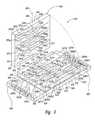
- FIG. 3is a partially exploded, partially schematic isometric illustration of a package 310 that includes a support member 340 , a first microfeature device 320 , and a stacked second microfeature device 330 arranged in accordance with another embodiment of the invention.
- the first microfeature device 320has features arranged in exactly the same manner as the corresponding features of the second microfeature device 330 . Accordingly, any microfeature device having this arrangement can be stacked upon any other microfeature device having the same arrangement. In other words, the microfeature device at the bottom of the stack need not have a different configuration than the microfeature device attached above.
- the first microfeature device 320can have a first bond pad surface 325 , with first device bond pads 321 positioned at least proximate to the first bond pad surface 325 .
- the first device bond pads 321 shown in FIG. 3are labeled with numerals 1-8.
- Each first device bond pad 321can be coupled to a first wirebond pad 328 with a corresponding first coupler 327 .
- the first couplers 327can include metal lines or other conductive structures located at or proximate to the first bond pad surface 325 .
- the first device bond pads 321are aligned with a device centerline 324 passing through the center of the first microfeature device 320 .
- the first device bond pads 321can be located off the device centerline 324 , as described in greater detail below with reference to FIG. 5 .
- the second microfeature device 330can have features arranged generally similarly to those of the first microfeature device 320 .
- the second microfeature device 330can include a second bond pad surface 335 , second device bond pads 331 (also labeled with numerals 1-8) at least proximate to the second bond pad surface 335 , and second wirebond pads 338 coupled to the second device bond pads 331 with second couplers 337 .
- the first and second microfeature devices 320 , 330can be stacked in a face-to-face arrangement on the support member 340 , as described in greater detail below.
- the support member 340includes package connection sites 343 , for example, bond pads that are accessible from the outside of the package 310 .
- Package connectors 342e.g., solder balls or other electrically conductive elements
- the package connection sites 343can be electrically coupled to the first wirebond pads 328 with wirebonds 350 . Accordingly, the wirebonds 350 can transmit signals between the package connection sites 343 and the first bond pads 321 .
- signals transmitted to and from the first device bond pads 321 of the first microfeature device 320are also transmitted to and from the corresponding second device bond pads 331 of the second microfeature device 330 . Accordingly, when the second microfeature device 330 is stacked face down on top of the first microfeature device 320 , each of the numbered second bond pads 331 aligns with the same correspondingly numbered first bond pad 321 of the first microfeature device 320 .
- the second device bond pads 331can be electrically connected to the corresponding first device bond pads 321 with electrically conductive members 323 , initially disposed on the first bond pads 321 .
- the electrically conductive members 323include solder balls, and in other embodiments, the electrically conductive members 323 include other structures. In any of these embodiments, the entire assembly can then be encapsulated with an encapsulant 111 (a small portion of which is shown in FIG. 3 ) in a manner generally similar to that shown in FIG. 2 .
- FIG. 4illustrates a partially exploded isometric view of a package 410 configured in accordance with another embodiment to the invention.
- the package 410includes first and second microfeature devices 420 , 430 having at least generally similar layouts, stacked face-to-face on a support member 440 .
- the first microfeature device 420can include a first bond pad surface 425 on or near which are positioned first bond device pads 421 (labeled with numerals 1-8) coupled to first wirebond pads 428 with first couplers 427 .
- each first device bond pad 421is coupled to a pair of first wirebond pads 428 with a coupler 427 that extends laterally to the left and right of the centrally positioned first device bond pad 421 .
- Wirebonds 450connect the wirebond pads 428 to package connection sites 443 .
- half the wirebonds 450connect to the first wirebond pads 428 located to the right of the first bond pads 421 , and half connect to the first wirebond pads 428 located to the left of the first bond pads 421 .
- the wirebonds 450are distributed in other manners.
- Microfeature devices having the foregoing arrangementcan be positioned on the bottom of the stack (e.g., in the position of the first microfeature device 420 ) or, by rotating the microfeature device and placing it face down, on the top of the stack (e.g., in the position of the second microfeature device 430 ).
- the second microfeature device 430includes a second bond pad surface 435 that carries second device bond pads 431 electrically coupled to second wirebond pads 438 with second couplers 437 .
- Those second wirebond pads 438 that are aligned with the wirebonds 450 belowcan include electrically conductive members 433 (e.g., solder balls) that physically couple the second microfeature device 430 to the first microfeature device 420 , and electrically couple the second device bond pads 431 to the corresponding first device bond pads 421 . Accordingly, signals transmitted to and/or received by the first device bond pads 421 are also transmitted to and/or received by the second bond pads 431 .
- electrically conductive members 433e.g., solder balls
- FIG. 5is a partially exploded, isometric view of a package 510 configured to provide communication links to a first microfeature device 520 and separate communication links to a stacked second microfeature device 530 .
- the first microfeature device 520includes ten active first device bond pads 521 (shown as first device bond pads 521 a - 521 j ) positioned along a first axis 570 that is offset from a centerline 526 of the first microfeature device 520 .
- the first microfeature device 520can also include corresponding first intermediate bond pads 522 (shown as first intermediate bond pads 522 a, 522 c - 522 j ) that are aligned (with the exception of first intermediate bond pad 522 g ) along a second axis 571 .
- the second axis 571is mirrored relative to the first axis 570 about the centerline 526 .
- the first device bond pads 521can be connected to first wirebond pads 528 with couplers 527 .
- Wirebonds 550can electrically couple the first wirebond pads 528 (and therefore, the first bond pads 521 ) to a support member 540 .
- the second microfeature device 530can have a layout identical to that of the first microfeature device 520 , with ten active second device bond pads 531 a - 531 j aligned along a first axis 580 , and corresponding second intermediate bond pads 532 a - 532 j generally aligned along a second axis 581 .
- the first axis 580 and the second axis 581can be equidistant from a centerline 536 of the second microfeature device 530 .
- the second microfeature device 530when the second microfeature device 530 is positioned above the first microfeature device 520 , it is rotated so that the second device bond pads 531 align with the correspondingly numbered first intermediate bond pads 522 , and the second intermediate bond pads 532 align with the correspondingly numbered first device bond pads 521 .
- Some signals transmitted to/from the package 510are shared by the first microfeature device 520 and the second microfeature device 530 and are accordingly transmitted via both the first device bond pads 521 and the correspondingly numbered second device bond pads 531 .
- signals transmitted via the first device bond pads 521 a - e, i and jare also transmitted via the corresponding second device bond pads 531 a - e, i and j , respectively.
- the couplers 527 for these bond padsconnect these bond pads to the correspondingly numbered intermediate bond pads 522 , 532 mirrored across the device centerlines 526 , 536 .
- Electrically conductive members 533disposed on the first intermediate bond pads 522 electrically connect the first bond pads 521 of the first microfeature device 520 to the corresponding second bond pads 531 of the second microfeature device 530 .
- signals transmitted to/from the first device bond pad 521 aare also transmitted to/from the second device bond pad 531 a via an electrically conductive member 533 disposed between the first intermediate bond pad 522 a and the second device bond pad 531 a.
- signals transmitted to/from the package 510are transmitted to/from only the first microfeature device 520 and/or only the second microfeature device 530 .
- signals transmitted via the first device bond pads 521 f and 521 h of the first microfeature device 520are independent of signals transmitted via the second device bond pads 531 f and 531 h of the second microfeature device 530 .
- the first device bond pad 521 fis not electrically coupled to its corresponding first intermediate bond pad 522 f, but instead has an independent coupler 527 f 1 connected to a wirebond 550 f 1 at a first wirebond pad 528 f 1 .
- the first intermediate bond pad 522 fhas a separate coupler 527 f 2 connected at a corresponding first wirebond pad 528 f 2 to wirebond 550 f 2 .
- An electrically conductive member 533 at the first intermediate bond pad 522 felectrically couples the wirebond 550 f 2 to the second device bond pad 531 f of the second microfeature device 530 . Accordingly, signals transmitted via the first device bond pad 521 f are transmitted independently of signals transmitted via the second device bond pad 531 f.
- a generally similar though more complex arrangementis used to transmit signals via the first bond pad 521 h independently of signals transmitted via the second bond pad 531 h.
- the first bond pad 521 his coupled with a coupler 527 h 1 to a corresponding wirebond pad 528 h 1 and a corresponding wirebond 550 h 1 . Accordingly, signals travel to/from the first device bond pad 521 h directly via the coupler 527 h 1 and the wirebond 550 h 1 .
- a separate and electrically isolated coupler 527 h 2is connected between a first intermediate bond pad 522 h 2 and a wirebond pad 528 h 2 , which is coupled to a wirebond 550 h 2 .
- the first intermediate bond pad 522 h 2is positioned on a third axis 572 .
- Additional first intermediate bond pads 522 h 3 , 522 h and 522 h 4are electrically connected to each other and are positioned on the centerline 526 , the second axis 571 , and a fourth axis 573 , respectively.
- the fourth axis 573mirrors the third axis 572 about the centerline 526 .
- Electrically conductive members 533are disposed on the intermediate bond pads 522 h 2 , 522 h 3 and 522 h.
- Corresponding second intermediate bond pads 532 h 2 , 532 h, 532 h 3 and 532 h 4 on the second microfeature deviceare positioned to route electrical signals between the second device bond pad 531 h and the wirebond 550 h 2 , as follows: When the second microfeature device 530 is positioned face down on the first microfeature device 520 and physically and electrically coupled to it, signals travel to/from the second device bond pad 531 h along a path that includes the wirebond 550 h 2 , the coupler 527 h 2 , the first intermediate bond pad 522 h 2 , then to the corresponding second intermediate bond pad 532 h 4 (of the second microfeature device 530 ), then to the second intermediate bond 532 h 3 (of the second microfeature device 530 ) then to the corresponding first intermediate bond pad 522 h 3 (of the first microfeature device 520
- One feature of an arrangement of microfeature devices described above with reference to FIG. 5is that signals can be transmitted to/from some or all of the bond pads 521 of the first microfeature device 520 independently of signals transmitted to/from the corresponding bond pads 531 of the second microfeature device 530 .
- This featurecan increase the versatility of the package 510 because some or all aspects of the microfeature devices 520 , 530 can be independently controlled despite the fact that they are stacked in the same package 510 .
- microfeature devices 520 , 530Another feature of the microfeature devices 520 , 530 described above with reference to FIG. 5 is that both the first microfeature device 520 and the second microfeature device 530 can have identical feature layouts. Accordingly, even though each microfeature device 520 , 530 is configured to receive separate signals when combined in the package 510 , the devices themselves need not be manufactured to different specifications. An advantage of this arrangement is that costs associated with manufacturing and/or inventorying separate microfeature devices suitable for stacked packaging can be avoided, reducing the overall cost of the package 510 . Another advantage of this arrangement is that the likelihood for inadvertently connecting the microfeature devices in an incorrect manner can be reduced because the microfeature devices can have identical layouts.
Landscapes
- Engineering & Computer Science (AREA)
- Microelectronics & Electronic Packaging (AREA)
- Power Engineering (AREA)
- Computer Hardware Design (AREA)
- Physics & Mathematics (AREA)
- Condensed Matter Physics & Semiconductors (AREA)
- General Physics & Mathematics (AREA)
- Manufacturing & Machinery (AREA)
- Wire Bonding (AREA)
Abstract
Description
- This application is a divisional of U.S. application Ser. No. 12/820,704 filed Jun. 22, 2010, now U.S. Pat. No. 8,400,780, which is a divisional of U.S. application Ser. No. 11/416,740 filed May 3, 2006, now U.S. Pat. No. 7,742,313, which is a continuation of U.S. application Ser. No. 10/651,912 filed Aug. 29, 2003, now U.S. Pat. No. 7,071,421, each of which is incorporated herein by reference in its entirety.
- The present invention is directed generally to stacked microfeature devices and methods for manufacturing such packages.
- One method for increasing the density of microelectronic circuits for electronic devices (such as computers, portable phones, etc.) is to stack two or more microelectronic dies on top of each other. Accordingly, this arrangement can provide additional circuits within the same footprint normally occupied by a single die.
FIG. 1 is a partially schematic, cross-sectional elevational view of an existing stacked diepackage 10. Thepackage 10 includes asubstrate 40 that carries afirst die 20 and a stackedsecond die 30. Thefirst die 20 is attached to thesubstrate 40 with apaste layer 14. Aspacer 12 is attached to thefirst die 20 with afirst tape layer 13a.Thesecond die 30 is attached to thespacer 12 with asecond tape layer 13b. - The first die20 includes first
die bond pads 21 that are coupled to corresponding firstsubstrate bond pads 41awithfirst wirebonds 50a.The firstsubstrate bond pads 41aare coupled to externalsubstrate bond pads 41cwith vias. The externalsubstrate bond pads 41ceach have asubstrate solder ball 42 to provide communication between thefirst die 20 and devices located external to thepackage 10. Similarly, the second die30 includes seconddie bond pads 31 coupled to corresponding secondsubstrate bond pads 41bwithsecond wirebonds 50b.The secondsubstrate bond pads 41bare coupled to additional externalsubstrate bond pads 41cto provide communication between thesecond die 30 and devices external to the package. Once the first andsecond wirebonds substrate 40, thefirst die 20, and thesecond die 30 can be at least partially enclosed with anencapsulant 12 to protect these components. - One feature of an arrangement shown in
FIG. 1 is that the overall thickness of thepackage 10 can be significantly greater than the combined thicknesses of thesubstrate 40, thefirst die 20, and thesecond die 30. As a result, thepackage 10 can be difficult to integrate into devices having very tight vertical clearances. Accordingly, the benefits of the stacked die arrangement provided to the standard size devices in which they are incorporated may not be available for very compact devices. FIG. 1 is a partially schematic, cross-sectional elevation view of a package having stacked microelectronic dies in accordance with the prior art.FIG. 2 is a partially schematic, cross-sectional elevation view of a package having dies stacked and coupled in accordance with an embodiment of the invention.FIG. 3 is a partially schematic, partially exploded isometric view of two dies positioned to be stacked in accordance with another embodiment of the invention.FIG. 4 is a partially schematic, partially exploded view of two dies positioned to be stacked in accordance with yet another embodiment of the invention.FIG. 5 is a partially schematic, partially exploded view of two dies having off-center bond pads and being positioned to be stacked in accordance with still another embodiment to the invention.- The present invention is directed to stacked microfeature devices and associated methods. The term “microfeature device” is used throughout to include a device formed from a substrate upon which and/or in which submicron circuits or components and/or data storage elements or layers are fabricated. Submicron features in the substrate include, but are not limited to, trenches, vias, lines, and holes. These features typically have a submicron width (e.g., ranging from, for example, 0.1 micron to 0.75 micron) generally transverse to a major surface (e.g., a front side or a back side) of the device. The term microfeature device is also used to include substrates upon which and/or in which micromechanical features are formed. Such features include read/write head features and other micromechanical features having submicron or supermicron dimensions. In many of these embodiments, the substrate is formed from suitable materials, including ceramics, and may support layers and/or other formations of other materials, including but not limited to metals, dielectric materials and photoresists.
- A microfeature device package in accordance with one aspect of the invention can include a first microfeature device having a plurality of first bond pads at least proximate to a first bond pad surface, and a second microfeature device having a plurality of second bond pads at least proximate to a second bond pad surface. The second bond pad surface can face toward the first bond pad surface. A package connection site can be positioned to provide electrical communication between the first microfeature device and components external to the device package. A wirebond can be coupled between at least one of the first bond pads and the package connection site, and an electrically conductive link can be coupled between the first microfeature device and at least one of the second bond pads of the second microfeature device.
- In a particular aspect of the invention, the wirebond is one of a plurality of wirebonds and all the wirebonds of the package are connected directly to the first microfeature device. In a further particular aspect of the invention, the first microfeature device includes an intermediate bond pad electrically coupled to the at least one first bond pad, and the electrically conductive link is connected between the intermediate bond pad and the at least one second bond pad of the second microfeature device. In yet another aspect of the invention, the first microfeature device includes an intermediate bond pad electrically isolated from the at least one first bond pad, and the electrically conductive link is connected between the intermediate bond pad and the at least one second bond pad of the second microfeature device.
- The present invention is also directed towards methods for forming a microfeature device package. In one aspect of the invention, the method includes positioning a first microfeature device at least proximate to a second microfeature device, with the first microfeature device having a first bond pad surface with a plurality of first bond pads at least proximate to the first bond pad surface, and with the second microfeature device having a second bond pad surface with a plurality of second bond pads at least proximate to the second bond pad surface. The first bond pad surface can be positioned to face toward the second bond pad surface. A wire bond can be coupled between at least one of the first bond pads and a package connection site that is positioned to provide electrical communication between the first microfeature device and components external to the device package. An electrically conductive link can be coupled between the first microfeature device and at least one of the second bond pads of the second microfeature device.
- In a particular aspect of the invention, the wire bond is one of a plurality of wire bonds and the method further includes connecting all the wire bonds of the package directly to the first microfeature device. In other aspects of the invention, the first microfeature device can include an intermediate bond pad electrically coupled to the at least one first bond pad, and coupling an electrically conductive link between the first microfeature device and the at least one second bond pad can include coupling the electrically conductive link between the intermediate bond pad and the at least one second bond pad. In yet another aspect of the invention, the intermediate bond pad is electrically isolated from the at least one first bond pad.
- Several specific details of the invention are set forth in the following description and in
FIGS. 2-5 to provide a thorough understanding of certain embodiments of the invention. One skilled in the art, however, will understand that the present invention may have additional embodiments, and that other embodiments of the invention may be practiced without several of the specific features explained in the following description. FIG. 2 is a partially schematic, cross-sectional illustration of apackage 110 having afirst microfeature device 120 and asecond microfeature device 130 stacked in accordance with an embodiment of the invention. In one aspect of this embodiment, all the wirebonds within thepackage 110 can be attached directly to thefirst microfeature device 120, with some wirebonds communicating only with thefirst microfeature device 120, and with others communicating only with thesecond microfeature device 130, via additional electrical links positioned between thefirst microfeature device 120 and thesecond microfeature device 130. In another embodiment, at least some of the wirebonds can be coupled to both thefirst microfeature device 120 and thesecond microfeature device 130. In both embodiments, thefirst microfeature device 120 can provide a platform that supports electrical links coupled to thesecond microfeature device 130. As described in greater detail below, this arrangement can reduce the overall thickness of thepackage 110 by eliminating wirebonds connected directly to thesecond microfeature device 130.- In one aspect of an embodiment shown in
FIG. 2 , thepackage 110 includes asupport member 140, for example, a printed circuit board. Thesupport member 140 can carry the first andsecond devices package 110. Accordingly, thesupport member 140 can have a plurality of package connection sites143, shown inFIG. 2 as firstpackage connection sites 143aand secondpackage connection sites 143boffset forward of the firstpackage connection sites 143a.Each of the package connection sites143 can include apackage connector 142 to provide for communication with elements external to thepackage 110. In one embodiment, thepackage connectors 142 include solder balls and in other embodiments, thepackage connectors 142 include other electrically conductive structures. In any of these embodiments, the firstpackage connection sites 143acan be coupled to first supportmember bond pads 141awith a vias that extend through thesupport member 140. The secondpackage connection sites 143bcan be coupled to corresponding second supportmember bond pads 141b,also with vias that extend through thesupport member 140. The first supportmember bond pads 141aand the second supportmember bond pads 141bare connected to thefirst microfeature device 120 and thesecond microfeature device 130, respectively, as described in greater detail below. - In one aspect of an embodiment shown in
FIG. 2 , thefirst microfeature device 120 can be attached to thesupport member 140 with apaste layer 114. In other embodiments, thefirst microfeature device 120 can be attached to thesupport member 140 with other arrangements. In any of these embodiments, thefirst microfeature device 120 can include firstdevice bond pads 121 that are electrically coupled to features located within thefirst microfeature device 120. The firstdevice bond pads 121 can be connected to the first supportmember bond pads 141awithfirst wirebonds 150a.In a particular aspect of this embodiment, each of thefirst wirebonds 150acan be attached to a stud bump (e.g., a gold stud bump) or other feature located at the corresponding firstdevice bond pad 121 to improve the physical and/or electrical characteristics of the connection between the wirebond150aand the firstdevice bond pad 121. In other embodiments, thefirst wirebond 150acan be attached directly to the firstdevice bond pad 121. In still a further aspect of this embodiment, thefirst wirebond 150acan be attached first to thesupport member 140 and then to thefirst microfeature device 120, for example, to reduce the extent of the wirebond loop. - The
first microfeature device 120 can also carryintermediate bond pads 122. In one aspect of this embodiment, some or all of theintermediate bond pads 122 are not electrically connected to features within thefirst microfeature device 120, but instead, provide an intermediate point in an electrical communication link between thesecond microfeature device 130 and thesupport member 140. In another embodiment, at least some of theintermediate bond pads 122 are electrically connected to corresponding first device bond pads122 (e.g., via a redistribution layer) or directly to features within thefirst microfeature device 120. In another embodiment, theintermediate bond pads 122 can be connected to the secondsubstrate bond pads 141bwithsecond wirebonds 150b.As described in greater detail below, thesecond microfeature device 130 can also be electrically coupled to theintermediate bond pads 122 to complete the communication link between the secondpackage connection sites 143blocated at thesupport member 140, and the features within thesecond microfeature device 130. - The
second microfeature device 130 can includesecond bond pads 131 that are electrically connected to features within thesecond microfeature device 130. In one aspect of an embodiment shown inFIG. 2 , thesecond bond pads 131 may not be aligned directly above theintermediate bond pads 122 located on thefirst microfeature device 120. Accordingly, thesecond microfeature device 130 can includeauxiliary bond pads 132 which are aligned with theintermediate bond pads 122. Theauxiliary bond pads 132 can be connected to thesecond bond pads 131 withcouplers 134. In one embodiment, thecouplers 134 are part of a redistribution layer, and in other embodiments, thecouplers 134 have other arrangements. In one aspect of an embodiment shown inFIG. 2 , the coupling between theauxiliary bond pads 132 and thesecond bond pads 131 can be at the surface of thesecond microfeature device 130. In other embodiments, the connection between thebond pads second microfeature device 130. In any of these embodiments, theauxiliary bond pad 132 can be connected to an electricallyconductive member 133 that is aligned with a corresponding one of theintermediate bond pads 122 on thefirst microfeature device 120 below. In one embodiment, the electricallyconductive member 133 includes a stud bump, (e.g., a gold stud bump, a copper stud bump or a solder bump) and in other embodiments, the electricallyconductive member 133 includes other structures. In any of these embodiments, the electricallyconductive member 133 can be physically and electrically bonded to theintermediate bond pad 122 and/or to the portion of thesecond wirebond 150battached to theintermediate bond pad 122. - In a particular aspect of an embodiment shown in
FIG. 2 , thepackage 110 is subjected to ultrasonic energy and/or an elevated temperature to secure the connection between theauxiliary bond pad 132 and theintermediate bond pad 122. In other embodiments, other techniques are used to secure this connection. In any of these embodiments, the connection between theauxiliary bond pad 132 and theintermediate bond pad 122 can both physically secure thesecond microfeature device 130 to thefirst microfeature device 120, and can provide electrical communication between the seconddevice bond pad 131 and the secondpackage connection site 143b.Once this connection is complete, anoptional encapsulant 111 can be disposed over thesupport member 140, thefirst microfeature device 120 and thesecond microfeature device 130 to protect these components. In one embodiment, theencapsulant 111 can include a no-sweep encapsulant, available from KNS of Willow Grove, Pa. In other embodiments, theencapsulant 111 can include other products. - One feature of an embodiment of the
package 110 described above with reference toFIG. 2 is that thesecond wirebonds 150bneed not extend around the outwardly facingedges 160 of thesecond microfeature device 130. Instead, thesecond wirebonds 150battach to theintermediate bond pads 122 of thefirst microfeature device 120, with the electricallyconductive member 133 providing the link to thesecond microfeature device 130. One advantage of this feature is that the overall thickness T of thepackage 110 can be reduced when compared with existing packages because theencapsulant 111 need not extend beyond thesecond microfeature device 130 by an amount necessary to envelope thesecond wirebond 150b.Instead, thesecond wirebond 150bis positioned between thefirst microfeature device 120 and thesecond microfeature device 130. Because the resultingpackage 110 is accordingly thinner than conventional structural die packages, it can more easily be installed in locations that require a low profile device. - Another advantage of the foregoing arrangement is that the
encapsulant 111 need not envelop the entiresecond microfeature device 130. For example, if thesecond microfeature device 130 includes afirst surface 135aand a second,oppositely facing surface 135b,thesecond surface 135bneed not be covered with theencapsulant 111. As a result the rate at which heat is transferred from thesecond microfeature device 130 can be enhanced, due to the exposedsecond surface 135b. - Another feature of an embodiment of the
package 110 described above with reference toFIG. 2 is that thepackage 110 can have packageouter edges 115 that are located more closely to the deviceouter edges 160 of thesecond microfeature device 130 than are the outer edges of existing packages. In particular, because thesecond wirebonds 150bneed not extend around the deviceouter edges 160, the packageouter edges 115 can be flush with the deviceouter edges 160, or can extend only a short distance outwardly from the deviceouter edges 160. Accordingly, the overall width W of thepackage 110 can also be reduced when compared with existing packages and thepackage 110 can accordingly be more easily installed in locations having tight lateral space constraints. - Still another feature of an embodiment of the
package 110 described above with reference toFIG. 2 is that all the wirebonds of thepackage 110 can be connected to thefirst microfeature device 120 and none connected to thesecond microfeature device 130. Accordingly, all the wirebonds of thepackage 110 can be connected in a single pass, e.g., thepackage 110 need not undergo two separate wirebonding procedures, one for thefirst microfeature device 120 and another for thesecond microfeature device 130. An advantage of this arrangement is that it can reduce the time and cost associated with producing thepackage 110. - In other embodiments, the
package 110 can have other configurations. For example, the first and secondmicrofeature devices device bond pads 131 arranged in a mirror image of the firstdevice bond pads 121. Signals dedicated to either the first or second microfeature device can be routed via arrangements generally similar to those described below with reference toFIG. 5 . In still further embodiments, thepackage 110 can include more than two microfeature devices. For example, in one embodiment, third or third and fourth microfeature devices can be stacked on thesecond microfeature device 130, with separate wirebonds routed to the third microfeature device. FIG. 3 is a partially exploded, partially schematic isometric illustration of apackage 310 that includes asupport member 340, afirst microfeature device 320, and a stackedsecond microfeature device 330 arranged in accordance with another embodiment of the invention. In one aspect of this embodiment, thefirst microfeature device 320 has features arranged in exactly the same manner as the corresponding features of thesecond microfeature device 330. Accordingly, any microfeature device having this arrangement can be stacked upon any other microfeature device having the same arrangement. In other words, the microfeature device at the bottom of the stack need not have a different configuration than the microfeature device attached above.- In one aspect of an embodiment shown in
FIG. 3 , thefirst microfeature device 320 can have a firstbond pad surface 325, with firstdevice bond pads 321 positioned at least proximate to the firstbond pad surface 325. For purposes of illustration, the firstdevice bond pads 321 shown inFIG. 3 are labeled with numerals 1-8. Each firstdevice bond pad 321 can be coupled to afirst wirebond pad 328 with a correspondingfirst coupler 327. Thefirst couplers 327 can include metal lines or other conductive structures located at or proximate to the firstbond pad surface 325. In one aspect of this embodiment, the firstdevice bond pads 321 are aligned with adevice centerline 324 passing through the center of thefirst microfeature device 320. In other embodiments, the firstdevice bond pads 321 can be located off thedevice centerline 324, as described in greater detail below with reference toFIG. 5 . - As described above, the
second microfeature device 330 can have features arranged generally similarly to those of thefirst microfeature device 320. Accordingly, thesecond microfeature device 330 can include a secondbond pad surface 335, second device bond pads331 (also labeled with numerals 1-8) at least proximate to the secondbond pad surface 335, andsecond wirebond pads 338 coupled to the seconddevice bond pads 331 withsecond couplers 337. The first and secondmicrofeature devices support member 340, as described in greater detail below. - In one aspect of an embodiment shown in
FIG. 3 , thesupport member 340 includespackage connection sites 343, for example, bond pads that are accessible from the outside of thepackage 310. Package connectors342 (e.g., solder balls or other electrically conductive elements) can be coupled to thepackage connection sites 343 to provide for electrical communication with components outside thepackage 310. Thepackage connection sites 343 can be electrically coupled to thefirst wirebond pads 328 with wirebonds350. Accordingly, thewirebonds 350 can transmit signals between thepackage connection sites 343 and thefirst bond pads 321. - In a particular aspect of an embodiment shown in
FIG. 3 , signals transmitted to and from the firstdevice bond pads 321 of thefirst microfeature device 320 are also transmitted to and from the corresponding seconddevice bond pads 331 of thesecond microfeature device 330. Accordingly, when thesecond microfeature device 330 is stacked face down on top of thefirst microfeature device 320, each of the numberedsecond bond pads 331 aligns with the same correspondingly numberedfirst bond pad 321 of thefirst microfeature device 320. The seconddevice bond pads 331 can be electrically connected to the corresponding firstdevice bond pads 321 with electricallyconductive members 323, initially disposed on thefirst bond pads 321. In one embodiment, the electricallyconductive members 323 include solder balls, and in other embodiments, the electricallyconductive members 323 include other structures. In any of these embodiments, the entire assembly can then be encapsulated with an encapsulant111 (a small portion of which is shown inFIG. 3 ) in a manner generally similar to that shown inFIG. 2 . FIG. 4 illustrates a partially exploded isometric view of apackage 410 configured in accordance with another embodiment to the invention. In one aspect of this embodiment, thepackage 410 includes first and secondmicrofeature devices support member 440. Accordingly, thefirst microfeature device 420 can include a firstbond pad surface 425 on or near which are positioned first bond device pads421 (labeled with numerals 1-8) coupled tofirst wirebond pads 428 withfirst couplers 427. In one aspect of this embodiment, each firstdevice bond pad 421 is coupled to a pair offirst wirebond pads 428 with acoupler 427 that extends laterally to the left and right of the centrally positioned firstdevice bond pad 421.Wirebonds 450 connect thewirebond pads 428 to packageconnection sites 443. In one aspect of this embodiment, half thewirebonds 450 connect to thefirst wirebond pads 428 located to the right of thefirst bond pads 421, and half connect to thefirst wirebond pads 428 located to the left of thefirst bond pads 421. In other embodiments, thewirebonds 450 are distributed in other manners.- Microfeature devices having the foregoing arrangement can be positioned on the bottom of the stack (e.g., in the position of the first microfeature device420) or, by rotating the microfeature device and placing it face down, on the top of the stack (e.g., in the position of the second microfeature device430). The
second microfeature device 430 includes a secondbond pad surface 435 that carries seconddevice bond pads 431 electrically coupled tosecond wirebond pads 438 withsecond couplers 437. Thosesecond wirebond pads 438 that are aligned with thewirebonds 450 below can include electrically conductive members433 (e.g., solder balls) that physically couple thesecond microfeature device 430 to thefirst microfeature device 420, and electrically couple the seconddevice bond pads 431 to the corresponding firstdevice bond pads 421. Accordingly, signals transmitted to and/or received by the firstdevice bond pads 421 are also transmitted to and/or received by thesecond bond pads 431. FIG. 5 is a partially exploded, isometric view of apackage 510 configured to provide communication links to afirst microfeature device 520 and separate communication links to a stackedsecond microfeature device 530. In one aspect of this embodiment, thefirst microfeature device 520 includes ten active first device bond pads521 (shown as first device bond pads521a-521j) positioned along afirst axis 570 that is offset from acenterline 526 of thefirst microfeature device 520. Thefirst microfeature device 520 can also include corresponding first intermediate bond pads522 (shown as firstintermediate bond pads intermediate bond pad 522g) along asecond axis 571. Thesecond axis 571 is mirrored relative to thefirst axis 570 about thecenterline 526. The first device bond pads521 can be connected tofirst wirebond pads 528 withcouplers 527.Wirebonds 550 can electrically couple the first wirebond pads528 (and therefore, the first bond pads521) to asupport member 540.- The
second microfeature device 530 can have a layout identical to that of thefirst microfeature device 520, with ten active second device bond pads531a-531jaligned along afirst axis 580, and corresponding second intermediate bond pads532a-532jgenerally aligned along asecond axis 581. Thefirst axis 580 and thesecond axis 581 can be equidistant from acenterline 536 of thesecond microfeature device 530. Accordingly, when thesecond microfeature device 530 is positioned above thefirst microfeature device 520, it is rotated so that the second device bond pads531 align with the correspondingly numbered first intermediate bond pads522, and the second intermediate bond pads532 align with the correspondingly numbered first device bond pads521. - Some signals transmitted to/from the
package 510 are shared by thefirst microfeature device 520 and thesecond microfeature device 530 and are accordingly transmitted via both the first device bond pads521 and the correspondingly numbered second device bond pads531. For example, signals transmitted via the first device bond pads521a-e, iandjare also transmitted via the corresponding second device bond pads531a-e, iandj, respectively. Accordingly, thecouplers 527 for these bond pads connect these bond pads to the correspondingly numbered intermediate bond pads522,532 mirrored across thedevice centerlines first microfeature device 520 to the corresponding second bond pads531 of thesecond microfeature device 530. For example, signals transmitted to/from the firstdevice bond pad 521aare also transmitted to/from the seconddevice bond pad 531avia an electricallyconductive member 533 disposed between the firstintermediate bond pad 522aand the seconddevice bond pad 531a. - Other signals transmitted to/from the
package 510 are transmitted to/from only thefirst microfeature device 520 and/or only thesecond microfeature device 530. For example, signals transmitted via the firstdevice bond pads first microfeature device 520 are independent of signals transmitted via the seconddevice bond pads second microfeature device 530. Accordingly, the firstdevice bond pad 521fis not electrically coupled to its corresponding firstintermediate bond pad 522f,but instead has an independent coupler527f1 connected to a wirebond550f1 at a first wirebond pad528f1. The firstintermediate bond pad 522fhas a separate coupler527f2 connected at a corresponding first wirebond pad528f2 to wirebond550f2. An electricallyconductive member 533 at the firstintermediate bond pad 522felectrically couples the wirebond550f2 to the seconddevice bond pad 531fof thesecond microfeature device 530. Accordingly, signals transmitted via the firstdevice bond pad 521fare transmitted independently of signals transmitted via the seconddevice bond pad 531f. - A generally similar though more complex arrangement is used to transmit signals via the
first bond pad 521hindependently of signals transmitted via thesecond bond pad 531h.Thefirst bond pad 521his coupled with a coupler527h1 to a corresponding wirebond pad528h1 and a corresponding wirebond550h1. Accordingly, signals travel to/from the firstdevice bond pad 521hdirectly via the coupler527h1 and the wirebond550h1. - A separate and electrically isolated coupler527h2 is connected between a first
intermediate bond pad 522h2 and a wirebond pad528h2, which is coupled to a wirebond550h2. The firstintermediate bond pad 522h2 is positioned on athird axis 572. Additional firstintermediate bond pads 522h centerline 526, thesecond axis 571, and afourth axis 573, respectively. Thefourth axis 573 mirrors thethird axis 572 about thecenterline 526. Electricallyconductive members 533 are disposed on theintermediate bond pads 522h 2,522h 3 and522h.Corresponding secondintermediate bond pads 532h h 3 and532h4 on the second microfeature device are positioned to route electrical signals between the seconddevice bond pad 531hand the wirebond550h2, as follows: When thesecond microfeature device 530 is positioned face down on thefirst microfeature device 520 and physically and electrically coupled to it, signals travel to/from the seconddevice bond pad 531halong a path that includes the wirebond550h2, the coupler527h2, the firstintermediate bond pad 522h2, then to the corresponding secondintermediate bond pad 532h4 (of the second microfeature device530), then to the secondintermediate bond 532h3 (of the second microfeature device530) then to the corresponding firstintermediate bond pad 522h3 (of the first microfeature device520) then to the firstintermediate bond pad 522hand finally to thesecond bond pad 531hof thesecond microfeature device 530. - One feature of an arrangement of microfeature devices described above with reference to
FIG. 5 is that signals can be transmitted to/from some or all of the bond pads521 of thefirst microfeature device 520 independently of signals transmitted to/from the corresponding bond pads531 of thesecond microfeature device 530. This feature can increase the versatility of thepackage 510 because some or all aspects of themicrofeature devices same package 510. - Another feature of the
microfeature devices FIG. 5 is that both thefirst microfeature device 520 and thesecond microfeature device 530 can have identical feature layouts. Accordingly, even though eachmicrofeature device package 510, the devices themselves need not be manufactured to different specifications. An advantage of this arrangement is that costs associated with manufacturing and/or inventorying separate microfeature devices suitable for stacked packaging can be avoided, reducing the overall cost of thepackage 510. Another advantage of this arrangement is that the likelihood for inadvertently connecting the microfeature devices in an incorrect manner can be reduced because the microfeature devices can have identical layouts. - From the foregoing, it will be appreciated that specific embodiments of the invention have been described herein for purposes of illustration, but that various modifications may be made without deviating from the spirit and scope of the invention. Accordingly, the invention is not limited except as by the appended claims.
Claims (11)
Priority Applications (5)
| Application Number | Priority Date | Filing Date | Title |
|---|---|---|---|
| US13/845,953US9515046B2 (en) | 2003-08-29 | 2013-03-18 | Stacked microfeature devices and associated methods |
| US15/368,158US10062667B2 (en) | 2003-08-29 | 2016-12-02 | Stacked microfeature devices and associated methods |
| US16/104,862US11373979B2 (en) | 2003-08-29 | 2018-08-17 | Stacked microfeature devices and associated methods |
| US17/850,122US11887970B2 (en) | 2003-08-29 | 2022-06-27 | Stacked microfeature devices and associated methods |
| US18/412,466US20240153917A1 (en) | 2003-08-29 | 2024-01-12 | Stacked microfeature devices and associated methods |
Applications Claiming Priority (4)
| Application Number | Priority Date | Filing Date | Title |
|---|---|---|---|
| US10/651,912US7071421B2 (en) | 2003-08-29 | 2003-08-29 | Stacked microfeature devices and associated methods |
| US11/416,740US7742313B2 (en) | 2003-08-29 | 2006-05-03 | Stacked microfeature devices |
| US12/820,704US8400780B2 (en) | 2003-08-29 | 2010-06-22 | Stacked microfeature devices |
| US13/845,953US9515046B2 (en) | 2003-08-29 | 2013-03-18 | Stacked microfeature devices and associated methods |
Related Parent Applications (1)
| Application Number | Title | Priority Date | Filing Date |
|---|---|---|---|
| US12/820,704DivisionUS8400780B2 (en) | 2003-08-29 | 2010-06-22 | Stacked microfeature devices |
Related Child Applications (1)
| Application Number | Title | Priority Date | Filing Date |
|---|---|---|---|
| US15/368,158ContinuationUS10062667B2 (en) | 2003-08-29 | 2016-12-02 | Stacked microfeature devices and associated methods |
Publications (2)
| Publication Number | Publication Date |
|---|---|
| US20130217183A1true US20130217183A1 (en) | 2013-08-22 |
| US9515046B2 US9515046B2 (en) | 2016-12-06 |
Family
ID=34217509
Family Applications (8)
| Application Number | Title | Priority Date | Filing Date |
|---|---|---|---|
| US10/651,912Expired - LifetimeUS7071421B2 (en) | 2003-08-29 | 2003-08-29 | Stacked microfeature devices and associated methods |
| US11/416,740Expired - LifetimeUS7742313B2 (en) | 2003-08-29 | 2006-05-03 | Stacked microfeature devices |
| US12/820,704Expired - Fee RelatedUS8400780B2 (en) | 2003-08-29 | 2010-06-22 | Stacked microfeature devices |
| US13/845,953Expired - Fee RelatedUS9515046B2 (en) | 2003-08-29 | 2013-03-18 | Stacked microfeature devices and associated methods |
| US15/368,158Expired - LifetimeUS10062667B2 (en) | 2003-08-29 | 2016-12-02 | Stacked microfeature devices and associated methods |
| US16/104,862Expired - LifetimeUS11373979B2 (en) | 2003-08-29 | 2018-08-17 | Stacked microfeature devices and associated methods |
| US17/850,122Expired - LifetimeUS11887970B2 (en) | 2003-08-29 | 2022-06-27 | Stacked microfeature devices and associated methods |
| US18/412,466AbandonedUS20240153917A1 (en) | 2003-08-29 | 2024-01-12 | Stacked microfeature devices and associated methods |
Family Applications Before (3)
| Application Number | Title | Priority Date | Filing Date |
|---|---|---|---|
| US10/651,912Expired - LifetimeUS7071421B2 (en) | 2003-08-29 | 2003-08-29 | Stacked microfeature devices and associated methods |
| US11/416,740Expired - LifetimeUS7742313B2 (en) | 2003-08-29 | 2006-05-03 | Stacked microfeature devices |
| US12/820,704Expired - Fee RelatedUS8400780B2 (en) | 2003-08-29 | 2010-06-22 | Stacked microfeature devices |
Family Applications After (4)
| Application Number | Title | Priority Date | Filing Date |
|---|---|---|---|
| US15/368,158Expired - LifetimeUS10062667B2 (en) | 2003-08-29 | 2016-12-02 | Stacked microfeature devices and associated methods |
| US16/104,862Expired - LifetimeUS11373979B2 (en) | 2003-08-29 | 2018-08-17 | Stacked microfeature devices and associated methods |
| US17/850,122Expired - LifetimeUS11887970B2 (en) | 2003-08-29 | 2022-06-27 | Stacked microfeature devices and associated methods |
| US18/412,466AbandonedUS20240153917A1 (en) | 2003-08-29 | 2024-01-12 | Stacked microfeature devices and associated methods |
Country Status (1)
| Country | Link |
|---|---|
| US (8) | US7071421B2 (en) |
Cited By (2)
| Publication number | Priority date | Publication date | Assignee | Title |
|---|---|---|---|---|
| US10062667B2 (en) | 2003-08-29 | 2018-08-28 | Micron Technology, Inc. | Stacked microfeature devices and associated methods |
| TWI708334B (en)* | 2019-11-07 | 2020-10-21 | 南亞科技股份有限公司 | Redistribution layer structure and semiconductor package |
Families Citing this family (34)
| Publication number | Priority date | Publication date | Assignee | Title |
|---|---|---|---|---|
| US7422930B2 (en)* | 2004-03-02 | 2008-09-09 | Infineon Technologies Ag | Integrated circuit with re-route layer and stacked die assembly |
| US7492039B2 (en) | 2004-08-19 | 2009-02-17 | Micron Technology, Inc. | Assemblies and multi-chip modules including stacked semiconductor dice having centrally located, wire bonded bond pads |
| SG119234A1 (en)* | 2004-07-29 | 2006-02-28 | Micron Technology Inc | Assemblies including stacked semiconductor dice having centrally located wire bonded bond pads |
| SG130055A1 (en)* | 2005-08-19 | 2007-03-20 | Micron Technology Inc | Microelectronic devices, stacked microelectronic devices, and methods for manufacturing microelectronic devices |
| SG130066A1 (en) | 2005-08-26 | 2007-03-20 | Micron Technology Inc | Microelectronic device packages, stacked microelectronic device packages, and methods for manufacturing microelectronic devices |
| US20070070608A1 (en)* | 2005-09-29 | 2007-03-29 | Skyworks Solutions, Inc. | Packaged electronic devices and process of manufacturing same |
| SG135066A1 (en)* | 2006-02-20 | 2007-09-28 | Micron Technology Inc | Semiconductor device assemblies including face-to-face semiconductor dice, systems including such assemblies, and methods for fabricating such assemblies |
| US7573137B2 (en)* | 2006-03-31 | 2009-08-11 | Texas Instruments Incorporated | Controlling flip-chip techniques for concurrent ball bonds in semiconductor devices |
| US7659608B2 (en)* | 2006-09-15 | 2010-02-09 | Stats Chippac Ltd. | Stacked die semiconductor device having circuit tape |
| KR100817073B1 (en)* | 2006-11-03 | 2008-03-26 | 삼성전자주식회사 | Semiconductor chip stack package with bending prevention reinforcement connected to the board |
| US7687897B2 (en)* | 2006-12-28 | 2010-03-30 | Stats Chippac Ltd. | Mountable integrated circuit package-in-package system with adhesive spacing structures |
| US7719122B2 (en)* | 2007-01-11 | 2010-05-18 | Taiwan Semiconductor Manufacturing Co., Ltd. | System-in-package packaging for minimizing bond wire contamination and yield loss |
| TWI447869B (en)* | 2007-05-15 | 2014-08-01 | Chipmos Technology Inc | Chip stacked package structure and applications thereof |
| US7696629B2 (en)* | 2007-04-30 | 2010-04-13 | Chipmos Technology Inc. | Chip-stacked package structure |
| US20080315436A1 (en)* | 2007-06-20 | 2008-12-25 | Broadcom Corporation | Semiconductor wafer that supports multiple packaging techniques |
| JP5205867B2 (en)* | 2007-08-27 | 2013-06-05 | 富士通セミコンダクター株式会社 | Semiconductor device and manufacturing method thereof |
| KR100950511B1 (en) | 2009-09-22 | 2010-03-30 | 테세라 리써치 엘엘씨 | Microelectronic assembly with impedance controlled wirebond and conductive reference element |
| KR100935854B1 (en) | 2009-09-22 | 2010-01-08 | 테세라 리써치 엘엘씨 | Microelectronic assembly with impedance controlled wirebond and reference wirebond |
| US8803305B2 (en)* | 2009-11-18 | 2014-08-12 | Qualcomm Incorporated | Hybrid package construction with wire bond and through silicon vias |
| US7927919B1 (en)* | 2009-12-03 | 2011-04-19 | Powertech Technology Inc. | Semiconductor packaging method to save interposer |
| TWI409933B (en)* | 2010-06-15 | 2013-09-21 | Powertech Technology Inc | Chip stacked package structure and its fabrication method |
| TWI502723B (en)* | 2010-06-18 | 2015-10-01 | Chipmos Technologies Inc | Multi-chip stack package structure |
| US8901747B2 (en) | 2010-07-29 | 2014-12-02 | Mosys, Inc. | Semiconductor chip layout |
| US8368216B2 (en)* | 2010-08-31 | 2013-02-05 | Advanced Semiconductor Engineering, Inc. | Semiconductor package |
| US8581377B2 (en) | 2010-09-16 | 2013-11-12 | Tessera, Inc. | TSOP with impedance control |
| US8786083B2 (en) | 2010-09-16 | 2014-07-22 | Tessera, Inc. | Impedance controlled packages with metal sheet or 2-layer RDL |
| US9136197B2 (en)* | 2010-09-16 | 2015-09-15 | Tessera, Inc. | Impedence controlled packages with metal sheet or 2-layer RDL |
| US8853708B2 (en) | 2010-09-16 | 2014-10-07 | Tessera, Inc. | Stacked multi-die packages with impedance control |
| TW201345353A (en)* | 2012-04-20 | 2013-11-01 | Hon Hai Prec Ind Co Ltd | Chip assembly and chip assembling method |
| KR102053349B1 (en)* | 2013-05-16 | 2019-12-06 | 삼성전자주식회사 | Semiconductor package |
| US9640521B2 (en)* | 2014-09-30 | 2017-05-02 | Taiwan Semiconductor Manufacturing Company, Ltd. | Multi-die package with bridge layer and method for making the same |
| US9502369B2 (en) | 2015-02-04 | 2016-11-22 | Micron Technology, Inc. | Semiconductor devices and packages |
| US9601374B2 (en)* | 2015-03-26 | 2017-03-21 | Micron Technology, Inc. | Semiconductor die assembly |
| US10978426B2 (en)* | 2018-12-31 | 2021-04-13 | Micron Technology, Inc. | Semiconductor packages with pass-through clock traces and associated systems and methods |
Citations (17)
| Publication number | Priority date | Publication date | Assignee | Title |
|---|---|---|---|---|
| US5445311A (en)* | 1992-06-30 | 1995-08-29 | Hughes Aircraft Company | Electrical interconnection substrate with both wire bond and solder contacts, and fabrication method |
| US6215182B1 (en)* | 1999-10-19 | 2001-04-10 | Fujitsu Limited | Semiconductor device and method for producing the same |
| US6335104B1 (en)* | 2000-02-22 | 2002-01-01 | International Business Machines Corporation | Method for preparing a conductive pad for electrical connection and conductive pad formed |
| US20020027295A1 (en)* | 2000-09-04 | 2002-03-07 | Fujitsu Limited | Stacked semiconductor device and method of producing the same |
| US6413797B2 (en)* | 1997-10-09 | 2002-07-02 | Rohm Co., Ltd. | Semiconductor device and method for making the same |
| US6522015B1 (en)* | 2000-09-26 | 2003-02-18 | Amkor Technology, Inc. | Micromachine stacked wirebonded package |
| US6548376B2 (en)* | 2001-08-30 | 2003-04-15 | Micron Technology, Inc. | Methods of thinning microelectronic workpieces |
| US6555917B1 (en)* | 2001-10-09 | 2003-04-29 | Amkor Technology, Inc. | Semiconductor package having stacked semiconductor chips and method of making the same |
| US20030127717A1 (en)* | 2002-01-09 | 2003-07-10 | Jen-Kuang Fang | Multi-chip stacking package |
| US20040063242A1 (en)* | 2002-09-17 | 2004-04-01 | Chippac, Inc. | Semiconductor multi-package module having package stacked over ball grid array package and having wire bond interconnect between stacked packages |
| US6836009B2 (en)* | 2002-08-08 | 2004-12-28 | Micron Technology, Inc. | Packaged microelectronic components |
| US6847105B2 (en)* | 2001-09-21 | 2005-01-25 | Micron Technology, Inc. | Bumping technology in stacked die configurations |
| US6906415B2 (en)* | 2002-06-27 | 2005-06-14 | Micron Technology, Inc. | Semiconductor device assemblies and packages including multiple semiconductor devices and methods |
| US7009304B2 (en)* | 2002-04-24 | 2006-03-07 | Renesas Technology Corp. | Resin-sealed semiconductor device |
| US7368810B2 (en)* | 2003-08-29 | 2008-05-06 | Micron Technology, Inc. | Invertible microfeature device packages |
| US20090206460A1 (en)* | 2007-10-30 | 2009-08-20 | Elaine Bautista Reyes | Intermediate Bond Pad for Stacked Semiconductor Chip Package |
| US8476117B2 (en)* | 2002-02-13 | 2013-07-02 | Micron Technology, Inc. | Methods and apparatus for a stacked-die interposer |
Family Cites Families (99)
| Publication number | Priority date | Publication date | Assignee | Title |
|---|---|---|---|---|
| USRE36469E (en)* | 1988-09-30 | 1999-12-28 | Micron Technology, Inc. | Packaging for semiconductor logic devices |
| US5145099A (en)* | 1990-07-13 | 1992-09-08 | Micron Technology, Inc. | Method for combining die attach and lead bond in the assembly of a semiconductor package |
| US5946553A (en)* | 1991-06-04 | 1999-08-31 | Micron Technology, Inc. | Process for manufacturing a semiconductor package with bi-substrate die |
| US5252857A (en)* | 1991-08-05 | 1993-10-12 | International Business Machines Corporation | Stacked DCA memory chips |
| KR940008327B1 (en)* | 1991-10-10 | 1994-09-12 | 삼성전자 주식회사 | Semiconductor package and its mounting method |
| US5128831A (en)* | 1991-10-31 | 1992-07-07 | Micron Technology, Inc. | High-density electronic package comprising stacked sub-modules which are electrically interconnected by solder-filled vias |
| US5616520A (en)* | 1992-03-30 | 1997-04-01 | Hitachi, Ltd. | Semiconductor integrated circuit device and fabrication method thereof |
| US5438224A (en)* | 1992-04-23 | 1995-08-01 | Motorola, Inc. | Integrated circuit package having a face-to-face IC chip arrangement |
| US5677566A (en)* | 1995-05-08 | 1997-10-14 | Micron Technology, Inc. | Semiconductor chip package |
| US6013948A (en)* | 1995-11-27 | 2000-01-11 | Micron Technology, Inc. | Stackable chip scale semiconductor package with mating contacts on opposed surfaces |
| US5673730A (en)* | 1996-01-24 | 1997-10-07 | Micron Technology, Inc. | Form tooling and method of forming semiconductor package leads |
| US6072236A (en)* | 1996-03-07 | 2000-06-06 | Micron Technology, Inc. | Micromachined chip scale package |
| JP2806357B2 (en)* | 1996-04-18 | 1998-09-30 | 日本電気株式会社 | Stack module |
| US5925930A (en)* | 1996-05-21 | 1999-07-20 | Micron Technology, Inc. | IC contacts with palladium layer and flexible conductive epoxy bumps |
| DE19626126C2 (en)* | 1996-06-28 | 1998-04-16 | Fraunhofer Ges Forschung | Method for forming a spatial chip arrangement and spatial chip arrangement |
| US5907769A (en)* | 1996-12-30 | 1999-05-25 | Micron Technology, Inc. | Leads under chip in conventional IC package |
| US6103547A (en)* | 1997-01-17 | 2000-08-15 | Micron Technology, Inc. | High speed IC package configuration |
| US5994166A (en)* | 1997-03-10 | 1999-11-30 | Micron Technology, Inc. | Method of constructing stacked packages |
| US6271582B1 (en)* | 1997-04-07 | 2001-08-07 | Micron Technology, Inc. | Interdigitated leads-over-chip lead frame, device, and method for supporting an integrated circuit die |
| US6008996A (en)* | 1997-04-07 | 1999-12-28 | Micron Technology, Inc. | Interdigitated leads-over-chip lead frame, device, and method for supporting an integrated circuit die |
| US5879965A (en)* | 1997-06-19 | 1999-03-09 | Micron Technology, Inc. | Plastic lead frames for semiconductor devices, packages including same, and methods of fabrication |
| US5955777A (en)* | 1997-07-02 | 1999-09-21 | Micron Technology, Inc. | Lead frame assemblies with voltage reference plane and IC packages including same |
| US6159764A (en)* | 1997-07-02 | 2000-12-12 | Micron Technology, Inc. | Varied-thickness heat sink for integrated circuit (IC) packages and method of fabricating IC packages |
| US5986209A (en)* | 1997-07-09 | 1999-11-16 | Micron Technology, Inc. | Package stack via bottom leaded plastic (BLP) packaging |
| US6107122A (en)* | 1997-08-04 | 2000-08-22 | Micron Technology, Inc. | Direct die contact (DDC) semiconductor package |
| US6048744A (en)* | 1997-09-15 | 2000-04-11 | Micron Technology, Inc. | Integrated circuit package alignment feature |
| US6103548A (en)* | 1997-09-17 | 2000-08-15 | Motorola, Inc. | Semiconductor device and method of manufacture |
| JP2954108B2 (en)* | 1997-09-22 | 1999-09-27 | 九州日本電気株式会社 | Semiconductor device and manufacturing method thereof |
| US6005286A (en)* | 1997-10-06 | 1999-12-21 | Micron Technology, Inc. | Increasing the gap between a lead frame and a semiconductor die |
| US20010000157A1 (en)* | 1997-10-16 | 2001-04-05 | Rohm Co., Ltd. | Semiconductor device and method of making the same |
| US6097087A (en)* | 1997-10-31 | 2000-08-01 | Micron Technology, Inc. | Semiconductor package including flex circuit, interconnects and dense array external contacts |
| US6175149B1 (en)* | 1998-02-13 | 2001-01-16 | Micron Technology, Inc. | Mounting multiple semiconductor dies in a package |
| US6297547B1 (en)* | 1998-02-13 | 2001-10-02 | Micron Technology Inc. | Mounting multiple semiconductor dies in a package |
| US6002165A (en)* | 1998-02-23 | 1999-12-14 | Micron Technology, Inc. | Multilayered lead frame for semiconductor packages |
| US6137063A (en)* | 1998-02-27 | 2000-10-24 | Micron Technology, Inc. | Electrical interconnections |
| US6429528B1 (en)* | 1998-02-27 | 2002-08-06 | Micron Technology, Inc. | Multichip semiconductor package |
| US6028365A (en)* | 1998-03-30 | 2000-02-22 | Micron Technology, Inc. | Integrated circuit package and method of fabrication |
| US5933713A (en)* | 1998-04-06 | 1999-08-03 | Micron Technology, Inc. | Method of forming overmolded chip scale package and resulting product |
| US6072233A (en)* | 1998-05-04 | 2000-06-06 | Micron Technology, Inc. | Stackable ball grid array package |
| US6329705B1 (en)* | 1998-05-20 | 2001-12-11 | Micron Technology, Inc. | Leadframes including offsets extending from a major plane thereof, packaged semiconductor devices including same, and method of designing and fabricating such leadframes |
| US5990566A (en)* | 1998-05-20 | 1999-11-23 | Micron Technology, Inc. | High density semiconductor package |
| US6020629A (en)* | 1998-06-05 | 2000-02-01 | Micron Technology, Inc. | Stacked semiconductor package and method of fabrication |
| US6075283A (en)* | 1998-07-06 | 2000-06-13 | Micron Technology, Inc. | Downset lead frame for semiconductor packages |
| US6124150A (en)* | 1998-08-20 | 2000-09-26 | Micron Technology, Inc. | Transverse hybrid LOC package |
| US6153929A (en)* | 1998-08-21 | 2000-11-28 | Micron Technology, Inc. | Low profile multi-IC package connector |
| US6169331B1 (en)* | 1998-08-28 | 2001-01-02 | Micron Technology, Inc. | Apparatus for electrically coupling bond pads of a microelectronic device |
| US6291894B1 (en)* | 1998-08-31 | 2001-09-18 | Micron Technology, Inc. | Method and apparatus for a semiconductor package for vertical surface mounting |
| US6261865B1 (en)* | 1998-10-06 | 2001-07-17 | Micron Technology, Inc. | Multi chip semiconductor package and method of construction |
| US6303985B1 (en)* | 1998-11-12 | 2001-10-16 | Micron Technology, Inc. | Semiconductor lead frame and package with stiffened mounting paddle |
| US6048755A (en)* | 1998-11-12 | 2000-04-11 | Micron Technology, Inc. | Method for fabricating BGA package using substrate with patterned solder mask open in die attach area |
| US6438224B1 (en) | 1998-11-12 | 2002-08-20 | Nms Communications Corporation | Tone detection |
| US6232666B1 (en)* | 1998-12-04 | 2001-05-15 | Mciron Technology, Inc. | Interconnect for packaging semiconductor dice and fabricating BGA packages |
| US6081429A (en)* | 1999-01-20 | 2000-06-27 | Micron Technology, Inc. | Test interposer for use with ball grid array packages assemblies and ball grid array packages including same and methods |
| JP2000243876A (en)* | 1999-02-23 | 2000-09-08 | Fujitsu Ltd | Semiconductor device and manufacturing method thereof |
| US6180426B1 (en)* | 1999-03-01 | 2001-01-30 | Mou-Shiung Lin | High performance sub-system design and assembly |
| US6310390B1 (en)* | 1999-04-08 | 2001-10-30 | Micron Technology, Inc. | BGA package and method of fabrication |
| US6544880B1 (en)* | 1999-06-14 | 2003-04-08 | Micron Technology, Inc. | Method of improving copper interconnects of semiconductor devices for bonding |
| JP2001068621A (en)* | 1999-06-21 | 2001-03-16 | Shinko Electric Ind Co Ltd | Semiconductor device and its manufacture |
| US6239489B1 (en)* | 1999-07-30 | 2001-05-29 | Micron Technology, Inc. | Reinforcement of lead bonding in microelectronics packages |
| US6294839B1 (en)* | 1999-08-30 | 2001-09-25 | Micron Technology, Inc. | Apparatus and methods of packaging and testing die |
| US6212767B1 (en)* | 1999-08-31 | 2001-04-10 | Micron Technology, Inc. | Assembling a stacked die package |
| US6303981B1 (en)* | 1999-09-01 | 2001-10-16 | Micron Technology, Inc. | Semiconductor package having stacked dice and leadframes and method of fabrication |
| US6605875B2 (en)* | 1999-12-30 | 2003-08-12 | Intel Corporation | Integrated circuit die having bond pads near adjacent sides to allow stacking of dice without regard to dice size |
| US6229202B1 (en)* | 2000-01-10 | 2001-05-08 | Micron Technology, Inc. | Semiconductor package having downset leadframe for reducing package bow |
| JP3768761B2 (en)* | 2000-01-31 | 2006-04-19 | 株式会社日立製作所 | Semiconductor device and manufacturing method thereof |
| US6531784B1 (en)* | 2000-06-02 | 2003-03-11 | Amkor Technology, Inc. | Semiconductor package with spacer strips |
| US6560117B2 (en)* | 2000-06-28 | 2003-05-06 | Micron Technology, Inc. | Packaged microelectronic die assemblies and methods of manufacture |
| US6552910B1 (en)* | 2000-06-28 | 2003-04-22 | Micron Technology, Inc. | Stacked-die assemblies with a plurality of microelectronic devices and methods of manufacture |
| US6607937B1 (en)* | 2000-08-23 | 2003-08-19 | Micron Technology, Inc. | Stacked microelectronic dies and methods for stacking microelectronic dies |
| US6548757B1 (en)* | 2000-08-28 | 2003-04-15 | Micron Technology, Inc. | Microelectronic device assemblies having a shielded input and methods for manufacturing and operating such microelectronic device assemblies |
| US6552416B1 (en)* | 2000-09-08 | 2003-04-22 | Amkor Technology, Inc. | Multiple die lead frame package with enhanced die-to-die interconnect routing using internal lead trace wiring |
| JP3640876B2 (en)* | 2000-09-19 | 2005-04-20 | 株式会社ルネサステクノロジ | Semiconductor device and mounting structure of semiconductor device |
| JP4780844B2 (en)* | 2001-03-05 | 2011-09-28 | Okiセミコンダクタ株式会社 | Semiconductor device |
| KR100401020B1 (en)* | 2001-03-09 | 2003-10-08 | 앰코 테크놀로지 코리아 주식회사 | Stacking structure of semiconductor chip and semiconductor package using it |
| SG106054A1 (en)* | 2001-04-17 | 2004-09-30 | Micron Technology Inc | Method and apparatus for package reduction in stacked chip and board assemblies |
| US20020153600A1 (en)* | 2001-04-19 | 2002-10-24 | Walton Advanced Electronics Ltd | Double sided chip package |
| US6610560B2 (en)* | 2001-05-11 | 2003-08-26 | Siliconware Precision Industries Co., Ltd. | Chip-on-chip based multi-chip module with molded underfill and method of fabricating the same |
| JP2002359346A (en)* | 2001-05-30 | 2002-12-13 | Sharp Corp | Semiconductor device and method of stacking semiconductor chips |
| US6700794B2 (en)* | 2001-07-26 | 2004-03-02 | Harris Corporation | Decoupling capacitor closely coupled with integrated circuit |
| US7518223B2 (en)* | 2001-08-24 | 2009-04-14 | Micron Technology, Inc. | Semiconductor devices and semiconductor device assemblies including a nonconfluent spacer layer |
| KR20030018204A (en)* | 2001-08-27 | 2003-03-06 | 삼성전자주식회사 | Multi chip package having spacer |
| DE10142119B4 (en)* | 2001-08-30 | 2007-07-26 | Infineon Technologies Ag | Electronic component and method for its production |
| DE10142117A1 (en)* | 2001-08-30 | 2003-03-27 | Infineon Technologies Ag | Electronic component with at least two stacked semiconductor chips and method for its production |
| JP2003185710A (en)* | 2001-10-03 | 2003-07-03 | Matsushita Electric Ind Co Ltd | Multi-chip module, semiconductor chip, and inter-chip connection test method of multi-chip module |
| US6569709B2 (en)* | 2001-10-15 | 2003-05-27 | Micron Technology, Inc. | Assemblies including stacked semiconductor devices separated a distance defined by adhesive material interposed therebetween, packages including the assemblies, and methods |
| US20030089998A1 (en)* | 2001-11-09 | 2003-05-15 | Chan Vincent K. | Direct interconnect multi-chip module, method for making the same and electronic package comprising same |
| US7332819B2 (en)* | 2002-01-09 | 2008-02-19 | Micron Technology, Inc. | Stacked die in die BGA package |
| US20030111716A1 (en)* | 2001-12-14 | 2003-06-19 | Kazuaki Ano | Wirebonded multichip module |
| US8258616B1 (en)* | 2002-01-16 | 2012-09-04 | Marvell International Ltd. | Semiconductor dice having a shielded area created under bond wires connecting pairs of bonding pads |
| US6635970B2 (en)* | 2002-02-06 | 2003-10-21 | International Business Machines Corporation | Power distribution design method for stacked flip-chip packages |
| US20030160311A1 (en)* | 2002-02-28 | 2003-08-28 | Aminuddin Ismail | Stacked die semiconductor device |
| US20030230796A1 (en)* | 2002-06-12 | 2003-12-18 | Aminuddin Ismail | Stacked die semiconductor device |
| US20040067606A1 (en)* | 2002-10-02 | 2004-04-08 | Fehr Gerald K. | Method for stack-packaging integrated circuit die using at least one die in the package as a spacer |
| KR100508682B1 (en)* | 2002-11-20 | 2005-08-17 | 삼성전자주식회사 | Stack chip package of heat emission type using dummy wire |
| WO2004109327A1 (en)* | 2003-06-04 | 2004-12-16 | Koninklijke Philips Electronics, N.V. | Redundant wire bonds for increasing transducer reliability |
| US7470997B2 (en)* | 2003-07-23 | 2008-12-30 | Megica Corporation | Wirebond pad for semiconductor chip or wafer |
| US7071421B2 (en) | 2003-08-29 | 2006-07-04 | Micron Technology, Inc. | Stacked microfeature devices and associated methods |
| US7492039B2 (en)* | 2004-08-19 | 2009-02-17 | Micron Technology, Inc. | Assemblies and multi-chip modules including stacked semiconductor dice having centrally located, wire bonded bond pads |
| US20110147910A1 (en)* | 2009-12-21 | 2011-06-23 | Micron Technology, Inc. | Method for stacking die in thin, small-outline package |
- 2003
- 2003-08-29USUS10/651,912patent/US7071421B2/ennot_activeExpired - Lifetime
- 2006
- 2006-05-03USUS11/416,740patent/US7742313B2/ennot_activeExpired - Lifetime
- 2010
- 2010-06-22USUS12/820,704patent/US8400780B2/ennot_activeExpired - Fee Related
- 2013
- 2013-03-18USUS13/845,953patent/US9515046B2/ennot_activeExpired - Fee Related
- 2016
- 2016-12-02USUS15/368,158patent/US10062667B2/ennot_activeExpired - Lifetime
- 2018
- 2018-08-17USUS16/104,862patent/US11373979B2/ennot_activeExpired - Lifetime
- 2022
- 2022-06-27USUS17/850,122patent/US11887970B2/ennot_activeExpired - Lifetime
- 2024
- 2024-01-12USUS18/412,466patent/US20240153917A1/ennot_activeAbandoned
Patent Citations (18)
| Publication number | Priority date | Publication date | Assignee | Title |
|---|---|---|---|---|
| US5445311A (en)* | 1992-06-30 | 1995-08-29 | Hughes Aircraft Company | Electrical interconnection substrate with both wire bond and solder contacts, and fabrication method |
| US6413797B2 (en)* | 1997-10-09 | 2002-07-02 | Rohm Co., Ltd. | Semiconductor device and method for making the same |
| US6215182B1 (en)* | 1999-10-19 | 2001-04-10 | Fujitsu Limited | Semiconductor device and method for producing the same |
| US6335104B1 (en)* | 2000-02-22 | 2002-01-01 | International Business Machines Corporation | Method for preparing a conductive pad for electrical connection and conductive pad formed |
| US20020027295A1 (en)* | 2000-09-04 | 2002-03-07 | Fujitsu Limited | Stacked semiconductor device and method of producing the same |
| US6522015B1 (en)* | 2000-09-26 | 2003-02-18 | Amkor Technology, Inc. | Micromachine stacked wirebonded package |
| US6548376B2 (en)* | 2001-08-30 | 2003-04-15 | Micron Technology, Inc. | Methods of thinning microelectronic workpieces |
| US6847105B2 (en)* | 2001-09-21 | 2005-01-25 | Micron Technology, Inc. | Bumping technology in stacked die configurations |
| US6555917B1 (en)* | 2001-10-09 | 2003-04-29 | Amkor Technology, Inc. | Semiconductor package having stacked semiconductor chips and method of making the same |
| US20030127717A1 (en)* | 2002-01-09 | 2003-07-10 | Jen-Kuang Fang | Multi-chip stacking package |
| US8476117B2 (en)* | 2002-02-13 | 2013-07-02 | Micron Technology, Inc. | Methods and apparatus for a stacked-die interposer |
| US7009304B2 (en)* | 2002-04-24 | 2006-03-07 | Renesas Technology Corp. | Resin-sealed semiconductor device |
| US6906415B2 (en)* | 2002-06-27 | 2005-06-14 | Micron Technology, Inc. | Semiconductor device assemblies and packages including multiple semiconductor devices and methods |
| US6836009B2 (en)* | 2002-08-08 | 2004-12-28 | Micron Technology, Inc. | Packaged microelectronic components |
| US20140141544A1 (en)* | 2002-08-08 | 2014-05-22 | Micron Technology, Inc. | Packaged microelectronic components |
| US20040063242A1 (en)* | 2002-09-17 | 2004-04-01 | Chippac, Inc. | Semiconductor multi-package module having package stacked over ball grid array package and having wire bond interconnect between stacked packages |
| US7368810B2 (en)* | 2003-08-29 | 2008-05-06 | Micron Technology, Inc. | Invertible microfeature device packages |
| US20090206460A1 (en)* | 2007-10-30 | 2009-08-20 | Elaine Bautista Reyes | Intermediate Bond Pad for Stacked Semiconductor Chip Package |
Cited By (4)
| Publication number | Priority date | Publication date | Assignee | Title |
|---|---|---|---|---|
| US10062667B2 (en) | 2003-08-29 | 2018-08-28 | Micron Technology, Inc. | Stacked microfeature devices and associated methods |
| US11373979B2 (en) | 2003-08-29 | 2022-06-28 | Micron Technology, Inc. | Stacked microfeature devices and associated methods |
| US11887970B2 (en) | 2003-08-29 | 2024-01-30 | Micron Technology, Inc. | Stacked microfeature devices and associated methods |
| TWI708334B (en)* | 2019-11-07 | 2020-10-21 | 南亞科技股份有限公司 | Redistribution layer structure and semiconductor package |
Also Published As
| Publication number | Publication date |
|---|---|
| US11887970B2 (en) | 2024-01-30 |
| US20170084585A1 (en) | 2017-03-23 |
| US20060201704A1 (en) | 2006-09-14 |
| US20180358331A1 (en) | 2018-12-13 |
| US20100258939A1 (en) | 2010-10-14 |
| US7071421B2 (en) | 2006-07-04 |
| US20240153917A1 (en) | 2024-05-09 |
| US7742313B2 (en) | 2010-06-22 |
| US9515046B2 (en) | 2016-12-06 |
| US10062667B2 (en) | 2018-08-28 |
| US20050045378A1 (en) | 2005-03-03 |
| US8400780B2 (en) | 2013-03-19 |
| US11373979B2 (en) | 2022-06-28 |
| US20230008716A1 (en) | 2023-01-12 |
Similar Documents
| Publication | Publication Date | Title |
|---|---|---|
| US11887970B2 (en) | Stacked microfeature devices and associated methods | |
| JP3356821B2 (en) | Laminated multi-chip module and manufacturing method | |
| US7732906B2 (en) | Semiconductor device | |
| US7944057B2 (en) | Bond pad rerouting element, rerouted semiconductor devices including the rerouting element, and assemblies including the rerouted semiconductor devices | |
| JP2819284B2 (en) | Semiconductor package substrate, method of manufacturing the same, and stacked semiconductor package using the substrate | |
| KR101009121B1 (en) | Microelectronic device having an intermediate contact for connecting to the insert substrate, and a method of packaging a microelectronic device having an intermediate contact | |
| US9461015B2 (en) | Enhanced stacked microelectronic assemblies with central contacts | |
| JP4072505B2 (en) | Stacked semiconductor package | |
| JP4808408B2 (en) | Multi-chip package, semiconductor device used for the same, and manufacturing method thereof | |
| US6812567B2 (en) | Semiconductor package and package stack made thereof | |
| US20020024146A1 (en) | Semiconductor device | |
| EP2731134A1 (en) | Multi-chip module connection by way of bridging blocks | |
| US8637975B1 (en) | Semiconductor device having lead wires connecting bonding pads formed on opposite sides of a core region forming a shield area | |
| CN101872749A (en) | Cavity chip package structure and package-on-package structure using the same | |
| US8975745B2 (en) | Packaged microelectronic devices recessed in support member cavities, and associated methods | |
| KR100482719B1 (en) | Semiconductor device | |
| JP2000049279A (en) | Semiconductor device | |
| US20090206460A1 (en) | Intermediate Bond Pad for Stacked Semiconductor Chip Package | |
| US6984882B2 (en) | Semiconductor device with reduced wiring paths between an array of semiconductor chip parts | |
| JPH10223683A (en) | Semiconductor module | |
| US20080157320A1 (en) | Laterally Interconnected IC Packages and Methods |
Legal Events
| Date | Code | Title | Description |
|---|---|---|---|
| FEPP | Fee payment procedure | Free format text:PAYOR NUMBER ASSIGNED (ORIGINAL EVENT CODE: ASPN); ENTITY STATUS OF PATENT OWNER: LARGE ENTITY | |
| AS | Assignment | Owner name:U.S. BANK NATIONAL ASSOCIATION, AS COLLATERAL AGENT, CALIFORNIA Free format text:SECURITY INTEREST;ASSIGNOR:MICRON TECHNOLOGY, INC.;REEL/FRAME:038669/0001 Effective date:20160426 Owner name:U.S. BANK NATIONAL ASSOCIATION, AS COLLATERAL AGEN Free format text:SECURITY INTEREST;ASSIGNOR:MICRON TECHNOLOGY, INC.;REEL/FRAME:038669/0001 Effective date:20160426 | |
| AS | Assignment | Owner name:MORGAN STANLEY SENIOR FUNDING, INC., AS COLLATERAL AGENT, MARYLAND Free format text:PATENT SECURITY AGREEMENT;ASSIGNOR:MICRON TECHNOLOGY, INC.;REEL/FRAME:038954/0001 Effective date:20160426 Owner name:MORGAN STANLEY SENIOR FUNDING, INC., AS COLLATERAL Free format text:PATENT SECURITY AGREEMENT;ASSIGNOR:MICRON TECHNOLOGY, INC.;REEL/FRAME:038954/0001 Effective date:20160426 | |
| STCF | Information on status: patent grant | Free format text:PATENTED CASE | |
| AS | Assignment | Owner name:U.S. BANK NATIONAL ASSOCIATION, AS COLLATERAL AGENT, CALIFORNIA Free format text:CORRECTIVE ASSIGNMENT TO CORRECT THE REPLACE ERRONEOUSLY FILED PATENT #7358718 WITH THE CORRECT PATENT #7358178 PREVIOUSLY RECORDED ON REEL 038669 FRAME 0001. ASSIGNOR(S) HEREBY CONFIRMS THE SECURITY INTEREST;ASSIGNOR:MICRON TECHNOLOGY, INC.;REEL/FRAME:043079/0001 Effective date:20160426 Owner name:U.S. BANK NATIONAL ASSOCIATION, AS COLLATERAL AGEN Free format text:CORRECTIVE ASSIGNMENT TO CORRECT THE REPLACE ERRONEOUSLY FILED PATENT #7358718 WITH THE CORRECT PATENT #7358178 PREVIOUSLY RECORDED ON REEL 038669 FRAME 0001. ASSIGNOR(S) HEREBY CONFIRMS THE SECURITY INTEREST;ASSIGNOR:MICRON TECHNOLOGY, INC.;REEL/FRAME:043079/0001 Effective date:20160426 | |
| AS | Assignment | Owner name:JPMORGAN CHASE BANK, N.A., AS COLLATERAL AGENT, ILLINOIS Free format text:SECURITY INTEREST;ASSIGNORS:MICRON TECHNOLOGY, INC.;MICRON SEMICONDUCTOR PRODUCTS, INC.;REEL/FRAME:047540/0001 Effective date:20180703 Owner name:JPMORGAN CHASE BANK, N.A., AS COLLATERAL AGENT, IL Free format text:SECURITY INTEREST;ASSIGNORS:MICRON TECHNOLOGY, INC.;MICRON SEMICONDUCTOR PRODUCTS, INC.;REEL/FRAME:047540/0001 Effective date:20180703 | |
| AS | Assignment | Owner name:MICRON TECHNOLOGY, INC., IDAHO Free format text:RELEASE BY SECURED PARTY;ASSIGNOR:U.S. BANK NATIONAL ASSOCIATION, AS COLLATERAL AGENT;REEL/FRAME:047243/0001 Effective date:20180629 | |
| AS | Assignment | Owner name:MICRON TECHNOLOGY, INC., IDAHO Free format text:RELEASE BY SECURED PARTY;ASSIGNOR:MORGAN STANLEY SENIOR FUNDING, INC., AS COLLATERAL AGENT;REEL/FRAME:050937/0001 Effective date:20190731 | |
| AS | Assignment | Owner name:MICRON SEMICONDUCTOR PRODUCTS, INC., IDAHO Free format text:RELEASE BY SECURED PARTY;ASSIGNOR:JPMORGAN CHASE BANK, N.A., AS COLLATERAL AGENT;REEL/FRAME:051028/0001 Effective date:20190731 Owner name:MICRON TECHNOLOGY, INC., IDAHO Free format text:RELEASE BY SECURED PARTY;ASSIGNOR:JPMORGAN CHASE BANK, N.A., AS COLLATERAL AGENT;REEL/FRAME:051028/0001 Effective date:20190731 | |
| MAFP | Maintenance fee payment | Free format text:PAYMENT OF MAINTENANCE FEE, 4TH YEAR, LARGE ENTITY (ORIGINAL EVENT CODE: M1551); ENTITY STATUS OF PATENT OWNER: LARGE ENTITY Year of fee payment:4 | |
| FEPP | Fee payment procedure | Free format text:MAINTENANCE FEE REMINDER MAILED (ORIGINAL EVENT CODE: REM.); ENTITY STATUS OF PATENT OWNER: LARGE ENTITY | |
| LAPS | Lapse for failure to pay maintenance fees | Free format text:PATENT EXPIRED FOR FAILURE TO PAY MAINTENANCE FEES (ORIGINAL EVENT CODE: EXP.); ENTITY STATUS OF PATENT OWNER: LARGE ENTITY | |
| STCH | Information on status: patent discontinuation | Free format text:PATENT EXPIRED DUE TO NONPAYMENT OF MAINTENANCE FEES UNDER 37 CFR 1.362 | |
| FP | Lapsed due to failure to pay maintenance fee | Effective date:20241206 |