US20130207923A1 - Capacitive touch panel having protrusions formed between drive and/or sensor electrodes - Google Patents
Capacitive touch panel having protrusions formed between drive and/or sensor electrodesDownload PDFInfo
- Publication number
- US20130207923A1 US20130207923A1US13/370,087US201213370087AUS2013207923A1US 20130207923 A1US20130207923 A1US 20130207923A1US 201213370087 AUS201213370087 AUS 201213370087AUS 2013207923 A1US2013207923 A1US 2013207923A1
- Authority
- US
- United States
- Prior art keywords
- electrodes
- sensor electrodes
- protrusions
- elongated
- drive electrodes
- Prior art date
- Legal status (The legal status is an assumption and is not a legal conclusion. Google has not performed a legal analysis and makes no representation as to the accuracy of the status listed.)
- Granted
Links
Images


Classifications
- G—PHYSICS
- G06—COMPUTING OR CALCULATING; COUNTING
- G06F—ELECTRIC DIGITAL DATA PROCESSING
- G06F3/00—Input arrangements for transferring data to be processed into a form capable of being handled by the computer; Output arrangements for transferring data from processing unit to output unit, e.g. interface arrangements
- G06F3/01—Input arrangements or combined input and output arrangements for interaction between user and computer
- G06F3/03—Arrangements for converting the position or the displacement of a member into a coded form
- G06F3/041—Digitisers, e.g. for touch screens or touch pads, characterised by the transducing means
- G06F3/044—Digitisers, e.g. for touch screens or touch pads, characterised by the transducing means by capacitive means
- G06F3/0446—Digitisers, e.g. for touch screens or touch pads, characterised by the transducing means by capacitive means using a grid-like structure of electrodes in at least two directions, e.g. using row and column electrodes
- G—PHYSICS
- G06—COMPUTING OR CALCULATING; COUNTING
- G06F—ELECTRIC DIGITAL DATA PROCESSING
- G06F3/00—Input arrangements for transferring data to be processed into a form capable of being handled by the computer; Output arrangements for transferring data from processing unit to output unit, e.g. interface arrangements
- G06F3/01—Input arrangements or combined input and output arrangements for interaction between user and computer
- G06F3/03—Arrangements for converting the position or the displacement of a member into a coded form
- G06F3/041—Digitisers, e.g. for touch screens or touch pads, characterised by the transducing means
- G06F3/044—Digitisers, e.g. for touch screens or touch pads, characterised by the transducing means by capacitive means
- G06F3/0443—Digitisers, e.g. for touch screens or touch pads, characterised by the transducing means by capacitive means using a single layer of sensing electrodes
- G—PHYSICS
- G06—COMPUTING OR CALCULATING; COUNTING
- G06F—ELECTRIC DIGITAL DATA PROCESSING
- G06F2203/00—Indexing scheme relating to G06F3/00 - G06F3/048
- G06F2203/041—Indexing scheme relating to G06F3/041 - G06F3/045
- G06F2203/04111—Cross over in capacitive digitiser, i.e. details of structures for connecting electrodes of the sensing pattern where the connections cross each other, e.g. bridge structures comprising an insulating layer, or vias through substrate
Definitions
- a touch panelis a human machine interface (HMI) that allows an operator of an electronic device to provide input to the device using an instrument such as a finger, a stylus, and so forth.
- HMIhuman machine interface
- the operatormay use his or her finger to manipulate images on an electronic display, such as a display attached to a mobile computing device, a personal computer (PC), or a terminal connected to a network.
- the operatormay use two or more fingers simultaneously to provide unique commands, such as a zoom command, executed by moving two fingers away from one another; a shrink command, executed by moving two fingers toward one another; and so forth.
- a touch screenis an electronic visual display that incorporates a touch panel overlying a display to detect the presence and/or location of a touch within the display area of the screen.
- Touch screensare common in devices such as all-in-one computers, tablet computers, satellite navigation devices, gaming devices, and smartphones.
- a touch screenenables an operator to interact directly with information that is displayed by the display underlying the touch panel, rather than indirectly with a pointer controlled by a mouse or touchpad.
- Capacitive touch panelsare often used with touch screen devices.
- a capacitive touch panelgenerally includes an insulator, such as glass, coated with a transparent conductor, such as indium tin oxide (ITO). As the human body is also an electrical conductor, touching the surface of the panel results in a distortion of the panel's electrostatic field, measurable as a change in capacitance.
- ITOindium tin oxide
- the capacitive touch panelthat uses patterns, such as geometrical patterns, to provide spatial resolution for both a stylus and a finger is disclosed.
- the capacitive touch panelincludes elongated drive electrodes arranged next to one another and having a characteristic spacing between adjacent drive electrodes.
- the capacitive touch panelalso includes elongated sensor electrodes arranged next to one another across the drive electrodes and having a characteristic spacing between adjacent sensor electrodes.
- the characteristic spacing between the sensor electrodesmay be at least substantially greater than the characteristic spacing between the drive electrodes.
- the drive electrodes and/or the sensor electrodesinclude protrusions that extend into the spaces between adjacent electrodes.
- the sensor electrodesmay have a pitch based upon a touch diameter of a finger, wherein the touch panel is capable of sensing a stylus having a touch diameter substantially less than the touch diameter of the finger when the stylus is used in the spaces between adjacent sensor electrodes (e.g., due to capacitance between the stylus and the protrusions).
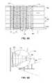
- FIG. 1is a diagrammatic illustration of electrode traces for a touch panel, and a graph illustrating a response generated when an instrument is moved across touch panel sensor electrodes in an X-direction with respect to the X-axis of the graph.
- FIG. 2is a diagrammatic illustration of electrodes for a touch panel, and a graph illustrating a response generated when an instrument is moved across touch panel sensor electrodes in an X-direction with respect to the X-axis of the graph, where the sensor electrodes include repeating protrusions in accordance with example implementations of the present disclosure.
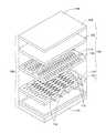
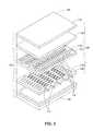
- FIG. 3is an exploded isometric view illustrating a touch screen assembly incorporating a touch panel having sensor and drive electrodes including repeating protrusions in accordance with example implementations of the present disclosure.
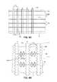
- FIG. 4Ais a top plan view illustrating sensor and drive electrodes for a touch panel, where the sensor electrodes include repeating protrusions extending past a center line between the sensor and drive electrodes in accordance with example implementations of the present disclosure.
- FIG. 4Bis a top plan view illustrating sensor electrodes for a touch panel, where the sensor electrodes include repeating protrusions, and each repeating protrusion includes finger-like protrusions in accordance with example implementations of the present disclosure.
- FIG. 4Cis a top plan view illustrating sensor and drive electrodes for a touch panel, where the sensor electrodes include protrusions in accordance with example implementations of the present disclosure.
- FIG. 4Dis a top plan view illustrating sensor and drive electrodes for a touch panel, where the sensor and drive electrodes include repeating protrusions in accordance with example implementations of the present disclosure.
- FIG. 4Eis a top plan view illustrating sensor and drive electrodes for a touch panel, where the sensor and drive electrodes include repeating protrusions extending past center lines between the sensor and drive electrodes in accordance with example implementations of the present disclosure.
- FIGS. 5A and 5Bare top plan views illustrating sensor and drive electrodes for a touch panel, where the sensor and drive electrodes are positioned on a single layer with jumpers connecting portions of the drive electrodes, and where the sensor electrodes include repeating protrusions in accordance with example implementations of the present disclosure.
- FIG. 6is a flow diagram illustrating a method of forming a touch panel in accordance with example implementations of the present disclosure.
- Cross-bar X and Y ITO patternsare typically used in mutual capacitance based capacitive touch panels.
- the ITO spacing between the parallel tracesis smaller than the diameter of the human finger. Because the human finger has a touch diameter in the range of about five to ten millimeters (5 mm-10 mm), the ITO spacing is typically less than five millimeters (5 mm) to provide adequate touch accuracy for the touch of one or more fingers and adequate resolution for a touch comprising two or more fingers (e.g., when the fingers are separated by about ten and one-half millimeters (10.5 mm) center to center).
- a writing accessorysuch as a stylus
- a styluswhich includes a generally pointed end having a smaller diameter than a finger.
- a styluswith, for example, about a one to two millimeter (1 mm-2 mm) touch diameter
- the responsiveness of a touch panel using five millimeter (5 mm) ITO spacingmay be unacceptable due to the existence of a large number of “dead zones,” or areas where touch coordinates do not change with stylus position and/or where a stylus signal is too weak to be measured between adjacent columns, leading to computed touch coordinates having large jumps and discontinuities.
- dead zonesor areas where touch coordinates do not change with stylus position and/or where a stylus signal is too weak to be measured between adjacent columns, leading to computed touch coordinates having large jumps and discontinuities.
- a touch paneluses patterns, such as geometrical patterns, to provide spatial resolution for both a stylus and a finger.
- Capacitive touch panelsconfigured in accordance with the present disclosure can allow a stylus to be used with a touch panel that has spacing between rows and/or columns configured for a finger without increasing the number of rows and/or columns in the capacitive touch panel.
- a five millimeter (5 mm) ITO trace pitchmay be capable of supporting a one millimeter (1 mm) stylus.
- the pitchcan be made larger than five millimeters (5 mm) (e.g., for supporting fingers).
- the required touch controller circuitry and powermay not be impacted significantly when supporting a stylus and/or when supporting large panels.
- FIGS. 2 through 5illustrate example mutual capacitance Projected Capacitive Touch (PCT) panels 100 in accordance with example implementations of the present disclosure.
- the capacitive touch panels 100can be used to interface with electronic devices including, but not necessarily limited to: large touch panel products, all-in-one computers, mobile computing devices (e.g., hand-held portable computers, Personal Digital Assistants (PDAs), laptop computers, netbook computers, tablet computers, and so forth), mobile telephone devices (e.g., cellular telephones and smartphones), portable game devices, portable media players, multimedia devices, satellite navigation devices (e.g., Global Positioning System (GPS) navigation devices), e-book reader devices (eReaders), Smart Television (TV) devices, surface computing devices (e.g., table top computers), Personal Computer (PC) devices, as well as with other devices that employ touch-based human interfaces.
- mobile computing devicese.g., hand-held portable computers, Personal Digital Assistants (PDAs), laptop computers, netbook computers, tablet computers, and so forth
- the capacitive touch panels 100may comprise ITO touch panels that include drive electrodes 102 , such as cross-bar ITO drive traces/tracks, arranged next to one another (e.g., along parallel tracks, generally parallel tracks, and so forth).
- the drive electrodes 102can be formed using highly conductive, optically transparent horizontal and/or vertical spines/bars 104 .
- the bars 104can reduce the resistance of the row and/or column traces, resulting in reduced phase shifts across the panel and reducing the complexity of the touch controller circuitry.
- the drive electrodes 102are elongated (e.g., extending along a longitudinal axis).
- each drive electrode 102may extend along an axis on a supporting surface, such as a substrate of a capacitive touch panel 100 .
- the drive electrodes 102have a pitch 106 (e.g., a substantially repetitive spacing between adjacent axes of the drive electrodes 102 ).
- the drive electrodes 102also have a characteristic spacing 108 comprising a minimum distance between adjacent edges of the drive electrodes 102 .
- the capacitive touch panels 100also include sensor electrodes 110 , such as cross-bar ITO sensor traces/tracks, arranged next to one another across the drive electrodes 102 (e.g., along parallel tracks, generally parallel tracks, and so forth).
- the sensor electrodes 110can be formed using highly conductive, optically transparent horizontal and/or vertical spines/bars 104 (e.g., as previously described).
- the sensor electrodes 110are elongated (e.g., extending along a longitudinal axis). For instance, each sensor electrode 110 may extend along an axis on a supporting surface, such as a substrate of a capacitive touch panel 100 .
- the sensor electrodes 110have a pitch 112 (e.g., a substantially repetitive spacing between adjacent axes of the sensor electrodes 110 ).
- the pitch 112is based upon the touch diameter of a finger.
- the pitch 112 between adjacent sensor electrodes 110may be about five millimeters (5 mm) center-to-center.
- a pitch 112 of five millimeters (5 mm)is provided by way of example only and is not meant to be restrictive of the present disclosure.
- other implementationsmay have a pitch 112 of more or less than five millimeters (5 mm).
- the sensor electrodes 110also have a characteristic spacing 114 comprising a minimum distance between adjacent edges of the sensor electrodes 110 .
- the characteristic spacing 114is measured between adjacent edges of the sensor electrodes 110 in a direction perpendicular to the sensor electrodes 110 (e.g., as shown in FIG. 2 ), while in other instances, the characteristic spacing 114 is measured between adjacent edges of the sensor electrodes 110 at an angle relative to the sensor electrodes 110 (e.g., as shown in FIG. 4A ).
- the drive electrodes 102 and the sensor electrodes 110define a coordinate system where each coordinate location (pixel) comprises a capacitor formed at each intersection between one of the drive electrodes 102 and one of the sensor electrodes 110 .
- the drive electrodes 102are configured to be connected to an electrical current source for generating a local electrostatic field at each capacitor, where a change in the local electrostatic field generated by a finger and/or a stylus at each capacitor causes a decrease in capacitance associated with a touch at the corresponding coordinate location. In this manner, more than one touch can be sensed at differing coordinate locations simultaneously (or at least substantially simultaneously).
- the drive electrodes 102can be driven by the electrical current source in parallel, e.g., where a set of different signals are provided to the drive electrodes 102 . In other implementations, the drive electrodes 102 can be driven by the electrical current source in series, e.g., where each drive electrode 102 or subset of drive electrodes 102 is driven one at a time.
- the sensor electrodes 110 and/or the drive electrodes 102include a series of one or more fins/protrusions 116 into the spaces between adjacent electrodes.
- the bars 104 of the sensor electrodes 110 and/or the drive electrodes 102can act as spines for the protrusions 116 .
- the protrusions 116may taper away from the sensor electrodes 110 and/or the drive electrodes 102 .
- the protrusions 116can be repeating and triangle-shaped (e.g., sawtoothed as shown in FIGS. 2 , 3 , 4 A, 4 D, 4 E, 5 A and 5 B).
- the protrusions 116can extend past a center line 118 defined between adjacent sensor electrodes 110 and/or adjacent drive electrodes 102 (e.g., as shown in FIGS. 4A , 4 B, and 4 E, where the protrusions 116 are interleaved).
- the protrusions 116are configured to provide a capacitive touch panel 100 with a broader and more linear touch profile in both the X and Y-directions (e.g., providing a signal that is suitable for interpolation). For example, with reference to FIG. 2 , as an instrument having a touch profile 120 moves across a capacitive touch panel 100 having protrusions 116 formed in a sawtooth pattern, the responses of the electrodes will be more linear/decrease less rapidly as the instrument moves into the spaces between the sensor electrodes 110 (e.g., when compared to the configuration with column bars shown in FIG. 1 ).
- a stylusmay have a uniformly changing coupling to adjacent column traces as it moves across the traces in the X-direction, and the computed touch coordinates will therefore change much more uniformly with minimal dead zones. This can improve signal reception such that the crossover point 122 between signals from adjacent sensor electrodes 110 may remain above the noise threshold 124 of the touch panel, resulting in a constant signal between the various coordinate locations.
- capacitive touch panels 100configured in accordance with the present disclosure can be used with a stylus having a touch diameter substantially less than the touch diameter of a finger, even when the electrodes of the touch panel comprise a pitch based upon the touch diameter of a finger (e.g., as previously described).
- the protrusions 116can be configured to provide the sensor electrodes 110 and/or the drive electrodes 102 with an increased perimeter with respect to the surface area occupied by the electrodes. This configuration can furnish an increased edge-length for the electrodes, which may reduce mutual capacitance between the sensor electrodes 110 and the drive electrodes 102 , and enhance the fringe capacitance of the sensor electrodes 110 and their mutual capacitance with an instrument such as a finger.
- the protrusions 116can be circuitously-shaped, and so forth. With reference to FIG.
- the protrusions 116can occupy a generally triangular area, having a number of primary/main protrusions 126 with one or more finger-like (thin rectangular) protrusions 128 extending from each main protrusion 126 .
- This configurationmay provide a more linear change in, for example, finger profile as an instrument moves away from one electrode and toward another electrode.
- FIG. 4Billustrates the spacing between the finger-like protrusions 128 increasing farther from the axes of sensor electrodes 110
- the spacing between the finger-like protrusions 128may also decrease farther from the axes of sensor electrodes 110 , may be relatively constant, or may increase and decrease in an alternating, random, or semi-random pattern.
- the finger-like protrusions 128may themselves have protrusions (e.g., exhibiting self-similarity), and so forth.
- the protrusions 116can occupy a generally rectangular area defining a rectangular gap therein (e.g., in the manner of a “double bar”). This configuration may serve to blur the sharp finger profile for a stylus, and slightly extend the coverage of the profile.
- the drive electrodes 102 and the sensor electrodes 110may each have differently shaped protrusions. For example, sawtooth-shaped protrusions may be used with the drive electrodes 102 , while finger-like protrusions may be used with the sensor electrodes 110 . Further, different rows of one kind/layer of electrode may have different protrusions.
- one row of sensor electrodes 110may have finger-like protrusions, while an adjacent row of sensor electrodes 110 may have sawtooth-shaped protrusions, and so forth.
- a dynamic reduction of the noise threshold for image zeroingmay also be used (e.g., to extend the finger profile for a stylus, and so forth).
- the characteristic spacing 114 of the sensor electrodes 110is at least substantially greater than the characteristic spacing 108 of the drive electrodes 102 .
- LCDLiquid Crystal Display
- the characteristic spacing 114 of the sensor electrodes 110is between about two times and five times (2-5 ⁇ ) the characteristic spacing 108 of the drive electrodes 102 .
- this spacingis provided by way of example only and is not meant to be restrictive of the present disclosure.
- the characteristic spacing 114 of the sensor electrodes 110can be less than two times (2 ⁇ ) (e.g., one and one-half times (1.5 ⁇ )) and/or more than five times (5 ⁇ ) (e.g., ten times (10 ⁇ )) the characteristic spacing 108 of the drive electrodes 102 .
- the sensor electrodes 110are electrically insulated from the drive electrodes 102 (e.g., using a dielectric layer, and so forth).
- the sensor electrodes 110may be provided on one substrate (e.g., comprising a sensor layer 130 disposed on a glass substrate), and the drive electrodes 102 may be provided on a separate substrate (e.g., comprising a drive layer 132 disposed on another substrate).
- the sensor layer 130can be disposed above the drive layer 132 (e.g., with respect to a touch surface).
- the sensor layer 130can be positioned closer to a touch surface than the drive layer 132 .
- this configurationis provided by way of example only and is not meant to be restrictive of the present disclosure.
- the drive layer 132is positioned closer to a touch surface than the sensor layer 130 , and/or where the sensor layer 130 and the drive layer 132 comprise the same layer.
- one or more jumpers 134can be used to connect portions of a drive electrode 102 together (e.g., as illustrated in FIGS. 5A and 5B ).
- jumperscan be used to connect portions of a sensor electrode 110 together.
- the touch screen assembly 138may include a display screen, such as an LCD screen 140 , where the sensor layer 130 and the drive layer 132 are sandwiched between the LCD screen 140 and a bonding layer 142 , e.g., with a protective cover 144 (e.g., glass) attached thereto.
- the protective cover 144may include a protective coating, an anti-reflective coating, and so forth.
- the protective cover 144may comprise a touch surface 146 , upon which an operator can use one or more fingers, a stylus, and so forth to input commands to the touch screen assembly 138 .
- the commandscan be used to manipulate graphics displayed by, for example, the LCD screen 140 . Further, the commands can be used as input to an electronic device connected to a capacitive touch panel 100 , such as a multimedia device or another electronic device (e.g., as previously described).
- example techniquesare described for furnishing capacitive touch panels having electrodes with protrusions extending into the spaces between the electrodes.
- FIG. 6depicts a process 600 , in an example implementation, for furnishing a capacitive touch panel, such as the capacitive touch panel 100 illustrated in FIGS. 2 through 5 and described above.
- elongated drive electrodes arranged next to one anotherare formed (Block 610 ).
- drive electrodes 102such as cross-bar ITO drive traces/tracks, are arranged next to one another.
- the drive electrodes 102can be formed on a substrate of a capacitive touch panel 100 using highly conductive, optically transparent horizontal and/or vertical bars 104 .
- protrusionsare formed into the spaces between adjacent drive electrodes (Block 612 ).
- the drive electrodes 102can include a series of one or more protrusions 116 into the spaces between adjacent drive electrodes 102 .
- bars 104 of the drive electrodes 102can act as spines for the protrusions 116 .
- sensor electrodes 110such as cross-bar ITO sensor traces/tracks, are arranged next to one another across drive electrodes 102 .
- the sensor electrodes 110can be formed on a substrate of a capacitive touch panel 100 using highly conductive, optically transparent horizontal and/or vertical bars 104 .
- protrusionsare formed into the spaces between adjacent sensor electrodes (Block 622 ).
- the sensor electrodes 110can include a series of one or more protrusions 116 into the spaces between adjacent sensor electrodes 110 .
- bars 104 of the sensor electrodes 110can act as spines for the protrusions 116 .
Landscapes
- Engineering & Computer Science (AREA)
- General Engineering & Computer Science (AREA)
- Theoretical Computer Science (AREA)
- Human Computer Interaction (AREA)
- Physics & Mathematics (AREA)
- General Physics & Mathematics (AREA)
- Position Input By Displaying (AREA)
- Switches That Are Operated By Magnetic Or Electric Fields (AREA)
Abstract
Description
- A touch panel is a human machine interface (HMI) that allows an operator of an electronic device to provide input to the device using an instrument such as a finger, a stylus, and so forth. For example, the operator may use his or her finger to manipulate images on an electronic display, such as a display attached to a mobile computing device, a personal computer (PC), or a terminal connected to a network. In some cases, the operator may use two or more fingers simultaneously to provide unique commands, such as a zoom command, executed by moving two fingers away from one another; a shrink command, executed by moving two fingers toward one another; and so forth.
- A touch screen is an electronic visual display that incorporates a touch panel overlying a display to detect the presence and/or location of a touch within the display area of the screen. Touch screens are common in devices such as all-in-one computers, tablet computers, satellite navigation devices, gaming devices, and smartphones. A touch screen enables an operator to interact directly with information that is displayed by the display underlying the touch panel, rather than indirectly with a pointer controlled by a mouse or touchpad. Capacitive touch panels are often used with touch screen devices. A capacitive touch panel generally includes an insulator, such as glass, coated with a transparent conductor, such as indium tin oxide (ITO). As the human body is also an electrical conductor, touching the surface of the panel results in a distortion of the panel's electrostatic field, measurable as a change in capacitance.
- A capacitive touch panel that uses patterns, such as geometrical patterns, to provide spatial resolution for both a stylus and a finger is disclosed. In one or more implementations, the capacitive touch panel includes elongated drive electrodes arranged next to one another and having a characteristic spacing between adjacent drive electrodes. The capacitive touch panel also includes elongated sensor electrodes arranged next to one another across the drive electrodes and having a characteristic spacing between adjacent sensor electrodes. The characteristic spacing between the sensor electrodes may be at least substantially greater than the characteristic spacing between the drive electrodes. The drive electrodes and/or the sensor electrodes include protrusions that extend into the spaces between adjacent electrodes. In some implementations, the sensor electrodes may have a pitch based upon a touch diameter of a finger, wherein the touch panel is capable of sensing a stylus having a touch diameter substantially less than the touch diameter of the finger when the stylus is used in the spaces between adjacent sensor electrodes (e.g., due to capacitance between the stylus and the protrusions).
- This Summary is provided to introduce a selection of concepts in a simplified form that are further described below in the Detailed Description. This Summary is not intended to identify key features or essential features of the claimed subject matter, nor is it intended to be used as an aid in determining the scope of the claimed subject matter.
- The Detailed Description is described with reference to the accompanying figures. The use of the same reference numbers in different instances in the description and the figures may indicate similar or identical items.
FIG. 1 is a diagrammatic illustration of electrode traces for a touch panel, and a graph illustrating a response generated when an instrument is moved across touch panel sensor electrodes in an X-direction with respect to the X-axis of the graph.FIG. 2 is a diagrammatic illustration of electrodes for a touch panel, and a graph illustrating a response generated when an instrument is moved across touch panel sensor electrodes in an X-direction with respect to the X-axis of the graph, where the sensor electrodes include repeating protrusions in accordance with example implementations of the present disclosure.FIG. 3 is an exploded isometric view illustrating a touch screen assembly incorporating a touch panel having sensor and drive electrodes including repeating protrusions in accordance with example implementations of the present disclosure.FIG. 4A is a top plan view illustrating sensor and drive electrodes for a touch panel, where the sensor electrodes include repeating protrusions extending past a center line between the sensor and drive electrodes in accordance with example implementations of the present disclosure.FIG. 4B is a top plan view illustrating sensor electrodes for a touch panel, where the sensor electrodes include repeating protrusions, and each repeating protrusion includes finger-like protrusions in accordance with example implementations of the present disclosure.FIG. 4C is a top plan view illustrating sensor and drive electrodes for a touch panel, where the sensor electrodes include protrusions in accordance with example implementations of the present disclosure.FIG. 4D is a top plan view illustrating sensor and drive electrodes for a touch panel, where the sensor and drive electrodes include repeating protrusions in accordance with example implementations of the present disclosure.FIG. 4E is a top plan view illustrating sensor and drive electrodes for a touch panel, where the sensor and drive electrodes include repeating protrusions extending past center lines between the sensor and drive electrodes in accordance with example implementations of the present disclosure.FIGS. 5A and 5B are top plan views illustrating sensor and drive electrodes for a touch panel, where the sensor and drive electrodes are positioned on a single layer with jumpers connecting portions of the drive electrodes, and where the sensor electrodes include repeating protrusions in accordance with example implementations of the present disclosure.FIG. 6 is a flow diagram illustrating a method of forming a touch panel in accordance with example implementations of the present disclosure.- Overview
- Cross-bar X and Y ITO patterns are typically used in mutual capacitance based capacitive touch panels. For capacitive touch panels use to sense finger touches, the ITO spacing between the parallel traces (for both vertical/column traces and horizontal/row traces) is smaller than the diameter of the human finger. Because the human finger has a touch diameter in the range of about five to ten millimeters (5 mm-10 mm), the ITO spacing is typically less than five millimeters (5 mm) to provide adequate touch accuracy for the touch of one or more fingers and adequate resolution for a touch comprising two or more fingers (e.g., when the fingers are separated by about ten and one-half millimeters (10.5 mm) center to center).
- It is often desirable to allow an operator of a touch panel to use a writing accessory, such as a stylus, which includes a generally pointed end having a smaller diameter than a finger. However, to support a stylus with, for example, about a one to two millimeter (1 mm-2 mm) touch diameter, the responsiveness of a touch panel using five millimeter (5 mm) ITO spacing may be unacceptable due to the existence of a large number of “dead zones,” or areas where touch coordinates do not change with stylus position and/or where a stylus signal is too weak to be measured between adjacent columns, leading to computed touch coordinates having large jumps and discontinuities. For example, with reference to
FIG. 1 , as an instrument having atouch profile 50 moves across a touch panel having sensor traces56 capacitively coupled withdrive traces 58, the response of thesensor traces 56 will decrease rapidly as the instrument moves between each sensor trace. This can lead to signal loss and/or provide a signal that is not suitable for interpolation when, for example, thecrossover point 52 between signals from adjacent electrodes falls below thenoise threshold 54 of the touch panel. - With large touch panels, it may be impractical to maintain a five millimeter (5 mm) pitch for traces used in rows and columns, since the number of traces becomes very large, and the traces then require more touch controller circuitry (e.g., more driver and associated Digital to Analog (D/A) circuitry, more Low Noise Amplifier (LNA) circuitry, and/or more Analog-to-Digital Conversion (ADC) circuitry). Making the pitch larger than about five millimeters (5 mm) for touch panels can result in the same inability to adequately track finger touches as described above with reference to tracking a stylus on a touch panel configured for a finger.
- Accordingly, a touch panel is described that uses patterns, such as geometrical patterns, to provide spatial resolution for both a stylus and a finger. Capacitive touch panels configured in accordance with the present disclosure can allow a stylus to be used with a touch panel that has spacing between rows and/or columns configured for a finger without increasing the number of rows and/or columns in the capacitive touch panel. For example, by using geometrical patterns for the ITO, a five millimeter (5 mm) ITO trace pitch may be capable of supporting a one millimeter (1 mm) stylus. Further, with large touch panels, the pitch can be made larger than five millimeters (5 mm) (e.g., for supporting fingers). Thus, the required touch controller circuitry and power may not be impacted significantly when supporting a stylus and/or when supporting large panels.
- Example Implementations
FIGS. 2 through 5 illustrate example mutual capacitance Projected Capacitive Touch (PCT)panels 100 in accordance with example implementations of the present disclosure. Thecapacitive touch panels 100 can be used to interface with electronic devices including, but not necessarily limited to: large touch panel products, all-in-one computers, mobile computing devices (e.g., hand-held portable computers, Personal Digital Assistants (PDAs), laptop computers, netbook computers, tablet computers, and so forth), mobile telephone devices (e.g., cellular telephones and smartphones), portable game devices, portable media players, multimedia devices, satellite navigation devices (e.g., Global Positioning System (GPS) navigation devices), e-book reader devices (eReaders), Smart Television (TV) devices, surface computing devices (e.g., table top computers), Personal Computer (PC) devices, as well as with other devices that employ touch-based human interfaces.- The
capacitive touch panels 100 may comprise ITO touch panels that includedrive electrodes 102, such as cross-bar ITO drive traces/tracks, arranged next to one another (e.g., along parallel tracks, generally parallel tracks, and so forth). In implementations, thedrive electrodes 102 can be formed using highly conductive, optically transparent horizontal and/or vertical spines/bars 104. Thebars 104 can reduce the resistance of the row and/or column traces, resulting in reduced phase shifts across the panel and reducing the complexity of the touch controller circuitry. Thedrive electrodes 102 are elongated (e.g., extending along a longitudinal axis). For example, eachdrive electrode 102 may extend along an axis on a supporting surface, such as a substrate of acapacitive touch panel 100. Thedrive electrodes 102 have a pitch106 (e.g., a substantially repetitive spacing between adjacent axes of the drive electrodes102). In implementations, thedrive electrodes 102 also have acharacteristic spacing 108 comprising a minimum distance between adjacent edges of thedrive electrodes 102. - The
capacitive touch panels 100 also includesensor electrodes 110, such as cross-bar ITO sensor traces/tracks, arranged next to one another across the drive electrodes102 (e.g., along parallel tracks, generally parallel tracks, and so forth). In implementations, thesensor electrodes 110 can be formed using highly conductive, optically transparent horizontal and/or vertical spines/bars104 (e.g., as previously described). Thesensor electrodes 110 are elongated (e.g., extending along a longitudinal axis). For instance, eachsensor electrode 110 may extend along an axis on a supporting surface, such as a substrate of acapacitive touch panel 100. Thesensor electrodes 110 have a pitch112 (e.g., a substantially repetitive spacing between adjacent axes of the sensor electrodes110). - In implementations, the
pitch 112 is based upon the touch diameter of a finger. For example, thepitch 112 betweenadjacent sensor electrodes 110 may be about five millimeters (5 mm) center-to-center. However, apitch 112 of five millimeters (5 mm) is provided by way of example only and is not meant to be restrictive of the present disclosure. Thus, other implementations may have apitch 112 of more or less than five millimeters (5 mm). In implementations, thesensor electrodes 110 also have acharacteristic spacing 114 comprising a minimum distance between adjacent edges of thesensor electrodes 110. In some instances, thecharacteristic spacing 114 is measured between adjacent edges of thesensor electrodes 110 in a direction perpendicular to the sensor electrodes110 (e.g., as shown inFIG. 2 ), while in other instances, thecharacteristic spacing 114 is measured between adjacent edges of thesensor electrodes 110 at an angle relative to the sensor electrodes110 (e.g., as shown inFIG. 4A ). - The
drive electrodes 102 and thesensor electrodes 110 define a coordinate system where each coordinate location (pixel) comprises a capacitor formed at each intersection between one of thedrive electrodes 102 and one of thesensor electrodes 110. Thus, thedrive electrodes 102 are configured to be connected to an electrical current source for generating a local electrostatic field at each capacitor, where a change in the local electrostatic field generated by a finger and/or a stylus at each capacitor causes a decrease in capacitance associated with a touch at the corresponding coordinate location. In this manner, more than one touch can be sensed at differing coordinate locations simultaneously (or at least substantially simultaneously). In implementations, thedrive electrodes 102 can be driven by the electrical current source in parallel, e.g., where a set of different signals are provided to thedrive electrodes 102. In other implementations, thedrive electrodes 102 can be driven by the electrical current source in series, e.g., where each drive electrode102 or subset ofdrive electrodes 102 is driven one at a time. - The
sensor electrodes 110 and/or thedrive electrodes 102 include a series of one or more fins/protrusions 116 into the spaces between adjacent electrodes. In implementations, thebars 104 of thesensor electrodes 110 and/or thedrive electrodes 102 can act as spines for theprotrusions 116. Theprotrusions 116 may taper away from thesensor electrodes 110 and/or thedrive electrodes 102. For example, theprotrusions 116 can be repeating and triangle-shaped (e.g., sawtoothed as shown inFIGS. 2 ,3,4A,4D,4E,5A and5B). Further, theprotrusions 116 can extend past acenter line 118 defined betweenadjacent sensor electrodes 110 and/or adjacent drive electrodes102 (e.g., as shown inFIGS. 4A ,4B, and4E, where theprotrusions 116 are interleaved). - The
protrusions 116 are configured to provide acapacitive touch panel 100 with a broader and more linear touch profile in both the X and Y-directions (e.g., providing a signal that is suitable for interpolation). For example, with reference toFIG. 2 , as an instrument having atouch profile 120 moves across acapacitive touch panel 100 havingprotrusions 116 formed in a sawtooth pattern, the responses of the electrodes will be more linear/decrease less rapidly as the instrument moves into the spaces between the sensor electrodes110 (e.g., when compared to the configuration with column bars shown inFIG. 1 ). For instance, a stylus may have a uniformly changing coupling to adjacent column traces as it moves across the traces in the X-direction, and the computed touch coordinates will therefore change much more uniformly with minimal dead zones. This can improve signal reception such that thecrossover point 122 between signals fromadjacent sensor electrodes 110 may remain above thenoise threshold 124 of the touch panel, resulting in a constant signal between the various coordinate locations. Thus,capacitive touch panels 100 configured in accordance with the present disclosure can be used with a stylus having a touch diameter substantially less than the touch diameter of a finger, even when the electrodes of the touch panel comprise a pitch based upon the touch diameter of a finger (e.g., as previously described). - The
protrusions 116 can be configured to provide thesensor electrodes 110 and/or thedrive electrodes 102 with an increased perimeter with respect to the surface area occupied by the electrodes. This configuration can furnish an increased edge-length for the electrodes, which may reduce mutual capacitance between thesensor electrodes 110 and thedrive electrodes 102, and enhance the fringe capacitance of thesensor electrodes 110 and their mutual capacitance with an instrument such as a finger. In some implementations, theprotrusions 116 can be circuitously-shaped, and so forth. With reference toFIG. 4B , theprotrusions 116 can occupy a generally triangular area, having a number of primary/main protrusions 126 with one or more finger-like (thin rectangular)protrusions 128 extending from eachmain protrusion 126. This configuration may provide a more linear change in, for example, finger profile as an instrument moves away from one electrode and toward another electrode. It should be noted that whileFIG. 4B illustrates the spacing between the finger-like protrusions 128 increasing farther from the axes ofsensor electrodes 110, the spacing between the finger-like protrusions 128 may also decrease farther from the axes ofsensor electrodes 110, may be relatively constant, or may increase and decrease in an alternating, random, or semi-random pattern. Further, it should be noted that the finger-like protrusions 128 may themselves have protrusions (e.g., exhibiting self-similarity), and so forth. - With reference to
FIG. 4C , theprotrusions 116 can occupy a generally rectangular area defining a rectangular gap therein (e.g., in the manner of a “double bar”). This configuration may serve to blur the sharp finger profile for a stylus, and slightly extend the coverage of the profile. It should be noted that thedrive electrodes 102 and thesensor electrodes 110 may each have differently shaped protrusions. For example, sawtooth-shaped protrusions may be used with thedrive electrodes 102, while finger-like protrusions may be used with thesensor electrodes 110. Further, different rows of one kind/layer of electrode may have different protrusions. For example, one row ofsensor electrodes 110 may have finger-like protrusions, while an adjacent row ofsensor electrodes 110 may have sawtooth-shaped protrusions, and so forth. In implementations, a dynamic reduction of the noise threshold for image zeroing may also be used (e.g., to extend the finger profile for a stylus, and so forth). - In implementations, the
characteristic spacing 114 of thesensor electrodes 110 is at least substantially greater than thecharacteristic spacing 108 of thedrive electrodes 102. For example, it may be desirable to maintain a greater spacing between thesensor electrodes 110 relative to the spacing between thedrive electrodes 102 in order to reduce column-to-column capacitance and provide sufficient fringe capacitance from the edges/sides of thesensor electrodes 110 to thedrive electrodes 102. Further, it may be desirable to maintain a tighter spacing between thedrive electrodes 102 relative to thesensor electrodes 110 in order to shield thesensor electrodes 110 from noise generated by other circuitry (e.g., noise from an underlying Liquid Crystal Display (LCD) screen, and so forth). In implementations, thecharacteristic spacing 114 of thesensor electrodes 110 is between about two times and five times (2-5×) thecharacteristic spacing 108 of thedrive electrodes 102. However, this spacing is provided by way of example only and is not meant to be restrictive of the present disclosure. Thus, thecharacteristic spacing 114 of thesensor electrodes 110 can be less than two times (2×) (e.g., one and one-half times (1.5×)) and/or more than five times (5×) (e.g., ten times (10×)) thecharacteristic spacing 108 of thedrive electrodes 102. - The
sensor electrodes 110 are electrically insulated from the drive electrodes102 (e.g., using a dielectric layer, and so forth). For example, thesensor electrodes 110 may be provided on one substrate (e.g., comprising asensor layer 130 disposed on a glass substrate), and thedrive electrodes 102 may be provided on a separate substrate (e.g., comprising adrive layer 132 disposed on another substrate). In this two-layer configuration, thesensor layer 130 can be disposed above the drive layer132 (e.g., with respect to a touch surface). For example, thesensor layer 130 can be positioned closer to a touch surface than thedrive layer 132. However, this configuration is provided by way of example only and is not meant to be restrictive of the present disclosure. Thus, other configurations can be provided where thedrive layer 132 is positioned closer to a touch surface than thesensor layer 130, and/or where thesensor layer 130 and thedrive layer 132 comprise the same layer. For instance, in a 1.5-layer implementation (e.g., where thedrive layer 132 and thesensor layer 130 are included on the same layer but physically separated from one another), one ormore jumpers 134 can be used to connect portions of adrive electrode 102 together (e.g., as illustrated inFIGS. 5A and 5B ). Similarly, jumpers can be used to connect portions of asensor electrode 110 together. - One or more
capacitive touch panels 100 can be included with atouch screen assembly 138. Thetouch screen assembly 138 may include a display screen, such as anLCD screen 140, where thesensor layer 130 and thedrive layer 132 are sandwiched between theLCD screen 140 and abonding layer 142, e.g., with a protective cover144 (e.g., glass) attached thereto. Theprotective cover 144 may include a protective coating, an anti-reflective coating, and so forth. Theprotective cover 144 may comprise atouch surface 146, upon which an operator can use one or more fingers, a stylus, and so forth to input commands to thetouch screen assembly 138. The commands can be used to manipulate graphics displayed by, for example, theLCD screen 140. Further, the commands can be used as input to an electronic device connected to acapacitive touch panel 100, such as a multimedia device or another electronic device (e.g., as previously described). - Example Process
- Referring now to
FIG. 6 , example techniques are described for furnishing capacitive touch panels having electrodes with protrusions extending into the spaces between the electrodes. FIG. 6 depicts aprocess 600, in an example implementation, for furnishing a capacitive touch panel, such as thecapacitive touch panel 100 illustrated inFIGS. 2 through 5 and described above. In theprocess 600 illustrated, elongated drive electrodes arranged next to one another are formed (Block610). For example, with reference toFIGS. 2 through 5 , driveelectrodes 102, such as cross-bar ITO drive traces/tracks, are arranged next to one another. Thedrive electrodes 102 can be formed on a substrate of acapacitive touch panel 100 using highly conductive, optically transparent horizontal and/orvertical bars 104. In some implementations, protrusions are formed into the spaces between adjacent drive electrodes (Block612). For instance, with continuing reference toFIGS. 2 through 5 , thedrive electrodes 102 can include a series of one ormore protrusions 116 into the spaces betweenadjacent drive electrodes 102. In some instances,bars 104 of thedrive electrodes 102 can act as spines for theprotrusions 116.- Next, elongated sensor electrodes arranged next to one another across the drive electrodes are formed (Block620). For example, with continuing reference to
FIGS. 2 through 5 ,sensor electrodes 110, such as cross-bar ITO sensor traces/tracks, are arranged next to one another acrossdrive electrodes 102. Thesensor electrodes 110 can be formed on a substrate of acapacitive touch panel 100 using highly conductive, optically transparent horizontal and/orvertical bars 104. Then, protrusions are formed into the spaces between adjacent sensor electrodes (Block622). For instance, with continuing reference toFIGS. 2 through 5 , thesensor electrodes 110 can include a series of one ormore protrusions 116 into the spaces betweenadjacent sensor electrodes 110. In some instances,bars 104 of thesensor electrodes 110 can act as spines for theprotrusions 116. - Although the subject matter has been described in language specific to structural features and/or process operations, it is to be understood that the subject matter defined in the appended claims is not necessarily limited to the specific features or acts described above. Rather, the specific features and acts described above are disclosed as example forms of implementing the claims.
Claims (20)
Priority Applications (2)
| Application Number | Priority Date | Filing Date | Title |
|---|---|---|---|
| US13/370,087US9116582B2 (en) | 2012-02-09 | 2012-02-09 | Capacitive touch panel having protrusions formed between drive and/or sensor electrodes |
| CN201310050663.XACN103246417B (en) | 2012-02-09 | 2013-02-08 | Capacitive touch panel with the projection between driving electrodes and/or sensing electrode |
Applications Claiming Priority (1)
| Application Number | Priority Date | Filing Date | Title |
|---|---|---|---|
| US13/370,087US9116582B2 (en) | 2012-02-09 | 2012-02-09 | Capacitive touch panel having protrusions formed between drive and/or sensor electrodes |
Publications (2)
| Publication Number | Publication Date |
|---|---|
| US20130207923A1true US20130207923A1 (en) | 2013-08-15 |
| US9116582B2 US9116582B2 (en) | 2015-08-25 |
Family
ID=48925963
Family Applications (1)
| Application Number | Title | Priority Date | Filing Date |
|---|---|---|---|
| US13/370,087Active2034-06-09US9116582B2 (en) | 2012-02-09 | 2012-02-09 | Capacitive touch panel having protrusions formed between drive and/or sensor electrodes |
Country Status (2)
| Country | Link |
|---|---|
| US (1) | US9116582B2 (en) |
| CN (1) | CN103246417B (en) |
Cited By (22)
| Publication number | Priority date | Publication date | Assignee | Title |
|---|---|---|---|---|
| US20140043260A1 (en)* | 2012-08-09 | 2014-02-13 | Eturbotouch Technology Inc. | Conductive Substrate and Touch Panel |
| US20140225859A1 (en)* | 2013-02-14 | 2014-08-14 | Broadcom Corporation | Mutual capacitive touch sensor pattern |
| US20140266261A1 (en)* | 2013-03-14 | 2014-09-18 | Microchip Technology Incorporated | Capacitive Sensor Electrode |
| CN104375726A (en)* | 2014-11-12 | 2015-02-25 | 江苏晟翔云数据信息技术有限公司 | Capacitive projected capacitive touch panel |
| EP2874050A1 (en)* | 2013-11-15 | 2015-05-20 | InnoLux Corporation | Touch panel |
| US20150193047A1 (en)* | 2013-09-10 | 2015-07-09 | Cypress Semiconductor Corporation | Interleaving sense elements of a capacitive-sense array |
| EP2916203A1 (en)* | 2014-03-03 | 2015-09-09 | Samsung Display Co., Ltd. | Touch panel and display apparatus including the same |
| US20150331526A1 (en)* | 2013-01-24 | 2015-11-19 | Toppan Printing Co., Ltd. | Touch panel and display apparatus |
| US20150346873A1 (en)* | 2012-07-23 | 2015-12-03 | Texas Instruments Incorporated | Capacitive touch panel having improved response characteristics |
| US20150378479A1 (en)* | 2013-03-22 | 2015-12-31 | Japan Display Inc. | Touch sensor device, display device and electronic equipment |
| US20160034071A1 (en)* | 2013-04-10 | 2016-02-04 | Abov Semiconductor Co., Ltd. | Capacitive type touch panel |
| US9411479B2 (en) | 2014-04-08 | 2016-08-09 | Samsung Display Co., Ltd. | Touch panel including touch sensor |
| WO2016191444A1 (en)* | 2015-05-28 | 2016-12-01 | Synaptics Incorporated | Matrix sensor for image touch sensing |
| US9612265B1 (en) | 2011-09-23 | 2017-04-04 | Cypress Semiconductor Corporation | Methods and apparatus to detect a conductive object |
| US20170205954A1 (en)* | 2016-01-18 | 2017-07-20 | Samsung Display Co., Ltd. | Touch panel and display device including the same |
| US9760212B2 (en) | 2013-09-30 | 2017-09-12 | Synaptics Incorported | Matrix sensor for image touch sensing |
| US9817523B2 (en) | 2012-02-09 | 2017-11-14 | Qualcomm Incorporated | Capacitive touch panel for mitigating and/or exaggerating floating condition effects |
| US10042489B2 (en) | 2013-09-30 | 2018-08-07 | Synaptics Incorporated | Matrix sensor for image touch sensing |
| US20180239457A1 (en)* | 2016-08-12 | 2018-08-23 | Boe Technology Group Co., Ltd. | Touch substrate, fabricating method thereof, display panel and display device |
| US20200233530A1 (en)* | 2017-01-03 | 2020-07-23 | Boe Technology Group Co., Ltd. | Touch panel, manufacturing method thereof, and touch display device |
| US11237670B2 (en)* | 2019-08-28 | 2022-02-01 | Hefei Xinsheng Optoelectronics Technology Co., Ltd. | Touch panel, method for manufacturing touch panel, and display device |
| US20220404930A1 (en)* | 2021-06-18 | 2022-12-22 | Sensel, Inc. | Interpolation electrode patterning for capacitive-grid touch sensor |
Families Citing this family (3)
| Publication number | Priority date | Publication date | Assignee | Title |
|---|---|---|---|---|
| US9916045B2 (en) | 2009-10-26 | 2018-03-13 | Amtel Corporation | Sense electrode design |
| CN104915045B (en)* | 2014-03-12 | 2019-01-04 | 深圳欧菲光科技股份有限公司 | Touch screen and its transparent conductive film, touch-control mobile terminal based on stylus |
| TWD192413S (en)* | 2017-04-26 | 2018-08-21 | 義隆電子股份有限公司 | Part of the conductive sheet |
Citations (7)
| Publication number | Priority date | Publication date | Assignee | Title |
|---|---|---|---|---|
| US4999462A (en)* | 1989-10-06 | 1991-03-12 | Summagraphics Corporation | Position determining and digitizing method and device |
| US20070262962A1 (en)* | 2006-05-10 | 2007-11-15 | Cypress Semiconductor Corporation | Apparatus and method for reducing charge time and power consumption of a sensing device |
| US20100045615A1 (en)* | 2008-08-21 | 2010-02-25 | Wacom Co., Ltd. | Meshed touchscreen pattern |
| US20100044122A1 (en)* | 2008-04-10 | 2010-02-25 | Atmel Corporation | Capacitive Touch Screen with Noise Suppression |
| US20100144391A1 (en)* | 2008-12-05 | 2010-06-10 | Shih Chang Chang | Integrated touch panel for a TFT display |
| US20130057511A1 (en)* | 2011-09-07 | 2013-03-07 | Synptics Incorporated | Capacitive sensing during non-display update times |
| US20130106762A1 (en)* | 2011-10-28 | 2013-05-02 | Atmel Corporation | Locking Active Stylus and Touch-Sensor Device |
Family Cites Families (7)
| Publication number | Priority date | Publication date | Assignee | Title |
|---|---|---|---|---|
| TWI354227B (en)* | 2007-09-13 | 2011-12-11 | Chimei Innolux Corp | Projecting capacitive touch sensing device, displa |
| CN101477430B (en)* | 2009-01-16 | 2012-11-07 | 汕头超声显示器(二厂)有限公司 | Condenser type touch screen |
| US8278571B2 (en) | 2009-04-03 | 2012-10-02 | Pixart Imaging Inc. | Capacitive touchscreen or touchpad for finger and active stylus |
| US9075484B2 (en) | 2009-06-02 | 2015-07-07 | Pixart Imaging Inc. | Sensor patterns for mutual capacitance touchscreens |
| US8723833B2 (en) | 2009-07-13 | 2014-05-13 | Microchip Technology Incorporated | Capacitive touch system with noise immunity |
| US9632628B2 (en)* | 2009-10-23 | 2017-04-25 | Atmel Corporation | Interdigitated touchscreen electrodes |
| US9817523B2 (en) | 2012-02-09 | 2017-11-14 | Qualcomm Incorporated | Capacitive touch panel for mitigating and/or exaggerating floating condition effects |
- 2012
- 2012-02-09USUS13/370,087patent/US9116582B2/enactiveActive
- 2013
- 2013-02-08CNCN201310050663.XApatent/CN103246417B/enactiveActive
Patent Citations (7)
| Publication number | Priority date | Publication date | Assignee | Title |
|---|---|---|---|---|
| US4999462A (en)* | 1989-10-06 | 1991-03-12 | Summagraphics Corporation | Position determining and digitizing method and device |
| US20070262962A1 (en)* | 2006-05-10 | 2007-11-15 | Cypress Semiconductor Corporation | Apparatus and method for reducing charge time and power consumption of a sensing device |
| US20100044122A1 (en)* | 2008-04-10 | 2010-02-25 | Atmel Corporation | Capacitive Touch Screen with Noise Suppression |
| US20100045615A1 (en)* | 2008-08-21 | 2010-02-25 | Wacom Co., Ltd. | Meshed touchscreen pattern |
| US20100144391A1 (en)* | 2008-12-05 | 2010-06-10 | Shih Chang Chang | Integrated touch panel for a TFT display |
| US20130057511A1 (en)* | 2011-09-07 | 2013-03-07 | Synptics Incorporated | Capacitive sensing during non-display update times |
| US20130106762A1 (en)* | 2011-10-28 | 2013-05-02 | Atmel Corporation | Locking Active Stylus and Touch-Sensor Device |
Cited By (39)
| Publication number | Priority date | Publication date | Assignee | Title |
|---|---|---|---|---|
| US9612265B1 (en) | 2011-09-23 | 2017-04-04 | Cypress Semiconductor Corporation | Methods and apparatus to detect a conductive object |
| US9817523B2 (en) | 2012-02-09 | 2017-11-14 | Qualcomm Incorporated | Capacitive touch panel for mitigating and/or exaggerating floating condition effects |
| US20150346873A1 (en)* | 2012-07-23 | 2015-12-03 | Texas Instruments Incorporated | Capacitive touch panel having improved response characteristics |
| US9383882B2 (en)* | 2012-08-09 | 2016-07-05 | Wistron Corporation | Conductive substrate and touch panel having conductive pads of different dimensions for impedance compensation and reduction |
| US20140043260A1 (en)* | 2012-08-09 | 2014-02-13 | Eturbotouch Technology Inc. | Conductive Substrate and Touch Panel |
| US20150331526A1 (en)* | 2013-01-24 | 2015-11-19 | Toppan Printing Co., Ltd. | Touch panel and display apparatus |
| US20140225859A1 (en)* | 2013-02-14 | 2014-08-14 | Broadcom Corporation | Mutual capacitive touch sensor pattern |
| US9869706B2 (en)* | 2013-03-14 | 2018-01-16 | Microchip Technology Incorporated | Capacitive sensor electrode |
| US20140266261A1 (en)* | 2013-03-14 | 2014-09-18 | Microchip Technology Incorporated | Capacitive Sensor Electrode |
| US20150378479A1 (en)* | 2013-03-22 | 2015-12-31 | Japan Display Inc. | Touch sensor device, display device and electronic equipment |
| US10379682B2 (en)* | 2013-03-22 | 2019-08-13 | Japan Display Inc. | Touch sensor device, display device and electronic equipment |
| US9535554B2 (en)* | 2013-04-10 | 2017-01-03 | Abov Semiconductor Co., Ltd. | Capacitive type touch panel |
| US20160034071A1 (en)* | 2013-04-10 | 2016-02-04 | Abov Semiconductor Co., Ltd. | Capacitive type touch panel |
| US20150193047A1 (en)* | 2013-09-10 | 2015-07-09 | Cypress Semiconductor Corporation | Interleaving sense elements of a capacitive-sense array |
| US9563318B2 (en)* | 2013-09-10 | 2017-02-07 | Monterey Research, Llc | Interleaving conductive elements of a capacitive-sense array |
| US10088951B2 (en) | 2013-09-30 | 2018-10-02 | Synaptics Incorporated | Matrix sensor for image touch sensing |
| US9760212B2 (en) | 2013-09-30 | 2017-09-12 | Synaptics Incorported | Matrix sensor for image touch sensing |
| US10042489B2 (en) | 2013-09-30 | 2018-08-07 | Synaptics Incorporated | Matrix sensor for image touch sensing |
| US9778790B2 (en) | 2013-09-30 | 2017-10-03 | Synaptics Incorporated | Matrix sensor for image touch sensing |
| EP2874050A1 (en)* | 2013-11-15 | 2015-05-20 | InnoLux Corporation | Touch panel |
| KR20150103777A (en)* | 2014-03-03 | 2015-09-14 | 삼성디스플레이 주식회사 | Touch panel and display apparatus including the same |
| KR102199213B1 (en)* | 2014-03-03 | 2021-01-07 | 삼성디스플레이 주식회사 | Touch panel and display apparatus including the same |
| EP2916203A1 (en)* | 2014-03-03 | 2015-09-09 | Samsung Display Co., Ltd. | Touch panel and display apparatus including the same |
| US9939968B2 (en) | 2014-03-03 | 2018-04-10 | Samsung Display Co., Ltd. | Touch panel and display apparatus including the same |
| US9411479B2 (en) | 2014-04-08 | 2016-08-09 | Samsung Display Co., Ltd. | Touch panel including touch sensor |
| CN104375726A (en)* | 2014-11-12 | 2015-02-25 | 江苏晟翔云数据信息技术有限公司 | Capacitive projected capacitive touch panel |
| WO2016191444A1 (en)* | 2015-05-28 | 2016-12-01 | Synaptics Incorporated | Matrix sensor for image touch sensing |
| KR20170086758A (en)* | 2016-01-18 | 2017-07-27 | 삼성디스플레이 주식회사 | Touch panel and display device having the same |
| US20170205954A1 (en)* | 2016-01-18 | 2017-07-20 | Samsung Display Co., Ltd. | Touch panel and display device including the same |
| US10234989B2 (en)* | 2016-01-18 | 2019-03-19 | Samsung Display Co., Ltd. | Touch panel and display device including the same |
| KR102535271B1 (en) | 2016-01-18 | 2023-05-23 | 삼성디스플레이 주식회사 | Touch panel and display device having the same |
| US20180239457A1 (en)* | 2016-08-12 | 2018-08-23 | Boe Technology Group Co., Ltd. | Touch substrate, fabricating method thereof, display panel and display device |
| US10572079B2 (en)* | 2016-08-12 | 2020-02-25 | Boe Technology Group Co., Ltd. | Touch substrate, fabricating method thereof, display panel and display device |
| US20200233530A1 (en)* | 2017-01-03 | 2020-07-23 | Boe Technology Group Co., Ltd. | Touch panel, manufacturing method thereof, and touch display device |
| US11023073B2 (en)* | 2017-01-03 | 2021-06-01 | Boe Technology Group Co., Ltd. | Touch panel, manufacturing method thereof, and touch display device |
| US11237670B2 (en)* | 2019-08-28 | 2022-02-01 | Hefei Xinsheng Optoelectronics Technology Co., Ltd. | Touch panel, method for manufacturing touch panel, and display device |
| US20220404930A1 (en)* | 2021-06-18 | 2022-12-22 | Sensel, Inc. | Interpolation electrode patterning for capacitive-grid touch sensor |
| US11893192B2 (en)* | 2021-06-18 | 2024-02-06 | Sensel, Inc. | Interpolation electrode patterning for capacitive-grid touch sensor |
| US20240134490A1 (en)* | 2021-06-18 | 2024-04-25 | Sensel, Inc. | Interpolation electrode patterning for capacitive-grid touch sensor |
Also Published As
| Publication number | Publication date |
|---|---|
| CN103246417A (en) | 2013-08-14 |
| US9116582B2 (en) | 2015-08-25 |
| CN103246417B (en) | 2017-09-26 |
Similar Documents
| Publication | Publication Date | Title |
|---|---|---|
| US9116582B2 (en) | Capacitive touch panel having protrusions formed between drive and/or sensor electrodes | |
| US9817523B2 (en) | Capacitive touch panel for mitigating and/or exaggerating floating condition effects | |
| TWI625667B (en) | Capacitive touch sensor panel, digital audio player, and method for shielding a capacitive touch sensor panel | |
| US10540043B2 (en) | Hybrid in-cell sensor topology | |
| EP3196741B1 (en) | Touch screen and touch positioning method therefor, and display device | |
| CN101464758B (en) | Touch pad electrode design | |
| US10013121B2 (en) | In-cell touch panel and display device with self-capacitance electrodes | |
| KR101663763B1 (en) | Display device with touch screen | |
| US9182865B2 (en) | Touch screen and touch panel including mutual capacitance type and self-capacitance type pixels, and driving method thereof | |
| US9927832B2 (en) | Input device having a reduced border region | |
| KR101304891B1 (en) | Capacitive touch sensitive panel and mobile terminal using the same | |
| US9568999B2 (en) | Method for representing a tactile image and touch screen apparatus for performing the method | |
| US20150220175A1 (en) | Capacitive touch panel and display device | |
| US20150370372A1 (en) | Capacitive touch panel having dielectric structures formed therein | |
| US20140104221A1 (en) | Capacitive touch panel sensor for mitigating effects of a floating condition | |
| CN105912176A (en) | Touch-control electrode structure, touch screen and display device | |
| US9423896B2 (en) | Method for representing a tactile image and touch screen apparatus for performing the method | |
| EP3204839B1 (en) | Digitizer sensor | |
| CN104375726A (en) | Capacitive projected capacitive touch panel | |
| CN103677477A (en) | Resistance type touch screen, touch point positioning method thereof and touch display device |
Legal Events
| Date | Code | Title | Description |
|---|---|---|---|
| AS | Assignment | Owner name:MAXIM INTEGRATED PRODUCTS, INC., CALIFORNIA Free format text:ASSIGNMENT OF ASSIGNORS INTEREST;ASSIGNORS:MOHINDRA, RISHI;SHEN, GUOZHONG;KNOX, KENNETH W.;REEL/FRAME:027681/0206 Effective date:20120206 | |
| AS | Assignment | Owner name:QUALCOMM TECHNOLOGIES, INC., CALIFORNIA Free format text:ASSIGNMENT OF ASSIGNORS INTEREST;ASSIGNOR:MAXIM INTEGRATED PRODUCTS, INC.;REEL/FRAME:036103/0682 Effective date:20150623 | |
| STCF | Information on status: patent grant | Free format text:PATENTED CASE | |
| AS | Assignment | Owner name:QUALCOMM TECHNOLOGIES, INC., CALIFORNIA Free format text:CORRECTIVE ASSIGNMENT TO CORRECT THE CA NOTARY CERTIFICATE INSIDE THE ASSINGMENT DOCUMENT AND ADDITION OF TWO NEW PATENT APPLICATIONS PREVIOUSLY RECORDED AT REEL: 036103 FRAME: 0682. ASSIGNOR(S) HEREBY CONFIRMS THE ASSIGNMENT;ASSIGNOR:MAXIM INTEGRATED PRODUCTS, INC.;REEL/FRAME:036526/0458 Effective date:20150723 | |
| AS | Assignment | Owner name:QUALCOMM INCORPORATED, CALIFORNIA Free format text:ASSIGNMENT OF ASSIGNORS INTEREST;ASSIGNOR:QUALCOMM TECHNOLOGIES, INC.;REEL/FRAME:039630/0817 Effective date:20160801 | |
| MAFP | Maintenance fee payment | Free format text:PAYMENT OF MAINTENANCE FEE, 4TH YEAR, LARGE ENTITY (ORIGINAL EVENT CODE: M1551); ENTITY STATUS OF PATENT OWNER: LARGE ENTITY Year of fee payment:4 | |
| MAFP | Maintenance fee payment | Free format text:PAYMENT OF MAINTENANCE FEE, 8TH YEAR, LARGE ENTITY (ORIGINAL EVENT CODE: M1552); ENTITY STATUS OF PATENT OWNER: LARGE ENTITY Year of fee payment:8 |