US20130207142A1 - Light emitter devices having improved chemical and physical resistance and related methods - Google Patents
Light emitter devices having improved chemical and physical resistance and related methodsDownload PDFInfo
- Publication number
- US20130207142A1 US20130207142A1US13/444,394US201213444394AUS2013207142A1US 20130207142 A1US20130207142 A1US 20130207142A1US 201213444394 AUS201213444394 AUS 201213444394AUS 2013207142 A1US2013207142 A1US 2013207142A1
- Authority
- US
- United States
- Prior art keywords
- barrier layer
- layer
- clear
- clear barrier
- glass
- Prior art date
- Legal status (The legal status is an assumption and is not a legal conclusion. Google has not performed a legal analysis and makes no representation as to the accuracy of the status listed.)
- Granted
Links
Images


Classifications
- H—ELECTRICITY
- H10—SEMICONDUCTOR DEVICES; ELECTRIC SOLID-STATE DEVICES NOT OTHERWISE PROVIDED FOR
- H10H—INORGANIC LIGHT-EMITTING SEMICONDUCTOR DEVICES HAVING POTENTIAL BARRIERS
- H10H20/00—Individual inorganic light-emitting semiconductor devices having potential barriers, e.g. light-emitting diodes [LED]
- H10H20/80—Constructional details
- H10H20/85—Packages
- H10H20/851—Wavelength conversion means
- H10H20/8515—Wavelength conversion means not being in contact with the bodies
- H—ELECTRICITY
- H01—ELECTRIC ELEMENTS
- H01L—SEMICONDUCTOR DEVICES NOT COVERED BY CLASS H10
- H01L2224/00—Indexing scheme for arrangements for connecting or disconnecting semiconductor or solid-state bodies and methods related thereto as covered by H01L24/00
- H01L2224/01—Means for bonding being attached to, or being formed on, the surface to be connected, e.g. chip-to-package, die-attach, "first-level" interconnects; Manufacturing methods related thereto
- H01L2224/42—Wire connectors; Manufacturing methods related thereto
- H01L2224/47—Structure, shape, material or disposition of the wire connectors after the connecting process
- H01L2224/48—Structure, shape, material or disposition of the wire connectors after the connecting process of an individual wire connector
- H01L2224/4805—Shape
- H01L2224/4809—Loop shape
- H01L2224/48091—Arched
- H—ELECTRICITY
- H01—ELECTRIC ELEMENTS
- H01L—SEMICONDUCTOR DEVICES NOT COVERED BY CLASS H10
- H01L2224/00—Indexing scheme for arrangements for connecting or disconnecting semiconductor or solid-state bodies and methods related thereto as covered by H01L24/00
- H01L2224/01—Means for bonding being attached to, or being formed on, the surface to be connected, e.g. chip-to-package, die-attach, "first-level" interconnects; Manufacturing methods related thereto
- H01L2224/42—Wire connectors; Manufacturing methods related thereto
- H01L2224/47—Structure, shape, material or disposition of the wire connectors after the connecting process
- H01L2224/48—Structure, shape, material or disposition of the wire connectors after the connecting process of an individual wire connector
- H01L2224/481—Disposition
- H01L2224/48135—Connecting between different semiconductor or solid-state bodies, i.e. chip-to-chip
- H01L2224/48137—Connecting between different semiconductor or solid-state bodies, i.e. chip-to-chip the bodies being arranged next to each other, e.g. on a common substrate
- H—ELECTRICITY
- H01—ELECTRIC ELEMENTS
- H01L—SEMICONDUCTOR DEVICES NOT COVERED BY CLASS H10
- H01L2224/00—Indexing scheme for arrangements for connecting or disconnecting semiconductor or solid-state bodies and methods related thereto as covered by H01L24/00
- H01L2224/01—Means for bonding being attached to, or being formed on, the surface to be connected, e.g. chip-to-package, die-attach, "first-level" interconnects; Manufacturing methods related thereto
- H01L2224/42—Wire connectors; Manufacturing methods related thereto
- H01L2224/47—Structure, shape, material or disposition of the wire connectors after the connecting process
- H01L2224/48—Structure, shape, material or disposition of the wire connectors after the connecting process of an individual wire connector
- H01L2224/481—Disposition
- H01L2224/48151—Connecting between a semiconductor or solid-state body and an item not being a semiconductor or solid-state body, e.g. chip-to-substrate, chip-to-passive
- H01L2224/48221—Connecting between a semiconductor or solid-state body and an item not being a semiconductor or solid-state body, e.g. chip-to-substrate, chip-to-passive the body and the item being stacked
- H01L2224/48245—Connecting between a semiconductor or solid-state body and an item not being a semiconductor or solid-state body, e.g. chip-to-substrate, chip-to-passive the body and the item being stacked the item being metallic
- H01L2224/48247—Connecting between a semiconductor or solid-state body and an item not being a semiconductor or solid-state body, e.g. chip-to-substrate, chip-to-passive the body and the item being stacked the item being metallic connecting the wire to a bond pad of the item
- H—ELECTRICITY
- H01—ELECTRIC ELEMENTS
- H01L—SEMICONDUCTOR DEVICES NOT COVERED BY CLASS H10
- H01L25/00—Assemblies consisting of a plurality of semiconductor or other solid state devices
- H01L25/03—Assemblies consisting of a plurality of semiconductor or other solid state devices all the devices being of a type provided for in a single subclass of subclasses H10B, H10D, H10F, H10H, H10K or H10N, e.g. assemblies of rectifier diodes
- H01L25/04—Assemblies consisting of a plurality of semiconductor or other solid state devices all the devices being of a type provided for in a single subclass of subclasses H10B, H10D, H10F, H10H, H10K or H10N, e.g. assemblies of rectifier diodes the devices not having separate containers
- H01L25/075—Assemblies consisting of a plurality of semiconductor or other solid state devices all the devices being of a type provided for in a single subclass of subclasses H10B, H10D, H10F, H10H, H10K or H10N, e.g. assemblies of rectifier diodes the devices not having separate containers the devices being of a type provided for in group H10H20/00
- H01L25/0753—Assemblies consisting of a plurality of semiconductor or other solid state devices all the devices being of a type provided for in a single subclass of subclasses H10B, H10D, H10F, H10H, H10K or H10N, e.g. assemblies of rectifier diodes the devices not having separate containers the devices being of a type provided for in group H10H20/00 the devices being arranged next to each other
- H—ELECTRICITY
- H01—ELECTRIC ELEMENTS
- H01L—SEMICONDUCTOR DEVICES NOT COVERED BY CLASS H10
- H01L2924/00—Indexing scheme for arrangements or methods for connecting or disconnecting semiconductor or solid-state bodies as covered by H01L24/00
- H01L2924/15—Details of package parts other than the semiconductor or other solid state devices to be connected
- H01L2924/181—Encapsulation
- H—ELECTRICITY
- H10—SEMICONDUCTOR DEVICES; ELECTRIC SOLID-STATE DEVICES NOT OTHERWISE PROVIDED FOR
- H10H—INORGANIC LIGHT-EMITTING SEMICONDUCTOR DEVICES HAVING POTENTIAL BARRIERS
- H10H20/00—Individual inorganic light-emitting semiconductor devices having potential barriers, e.g. light-emitting diodes [LED]
- H10H20/01—Manufacture or treatment
- H10H20/036—Manufacture or treatment of packages
- H—ELECTRICITY
- H10—SEMICONDUCTOR DEVICES; ELECTRIC SOLID-STATE DEVICES NOT OTHERWISE PROVIDED FOR
- H10H—INORGANIC LIGHT-EMITTING SEMICONDUCTOR DEVICES HAVING POTENTIAL BARRIERS
- H10H20/00—Individual inorganic light-emitting semiconductor devices having potential barriers, e.g. light-emitting diodes [LED]
- H10H20/80—Constructional details
- H10H20/85—Packages
- H10H20/851—Wavelength conversion means
- H10H20/8511—Wavelength conversion means characterised by their material, e.g. binder
- H10H20/8512—Wavelength conversion materials
- H10H20/8513—Wavelength conversion materials having two or more wavelength conversion materials
- H—ELECTRICITY
- H10—SEMICONDUCTOR DEVICES; ELECTRIC SOLID-STATE DEVICES NOT OTHERWISE PROVIDED FOR
- H10H—INORGANIC LIGHT-EMITTING SEMICONDUCTOR DEVICES HAVING POTENTIAL BARRIERS
- H10H20/00—Individual inorganic light-emitting semiconductor devices having potential barriers, e.g. light-emitting diodes [LED]
- H10H20/80—Constructional details
- H10H20/85—Packages
- H10H20/852—Encapsulations
- H10H20/853—Encapsulations characterised by their shape
Definitions
- the subject matter hereinrelates generally to light emitter devices and related methods. More particularly, the subject matter herein relates to light emitter devices having improved chemical and physical resistance and related methods.
- LEDsLight emitting diodes
- LEDscan be utilized in light emitter devices or packages for providing white light (e.g., perceived as being white or near-white), and they are developing as replacements for incandescent, fluorescent, and metal halide high-intensity discharge (HID) light products.
- Conventional emitter devices or packagescan incorporate components such as metallic traces or mounting surfaces which can become tarnished, corroded, or otherwise degraded when exposed to various undesirable chemicals and/or chemical vapors. Such chemicals and/or chemical vapors can enter conventional emitter devices, for example, by permeating an encapsulant filling material disposed over such components.
- undesirable chemicals and/or chemical vaporscan contain sulfur, sulfur-containing compounds (e.g., sulfides, sulfites, sulfates, SO x ), chlorine and bromine containing complexes, nitric oxide or nitrogen dioxides (e.g., NO x ), and oxidizing organic vapor compounds which can permeate the encapsulant and physically degrade various components within the emitter device by corroding, oxidizing, darkening, and/or tarnishing such components. Such degradation can adversely affect brightness, reliability, and/or thermal properties of conventional emitter devices over time and can further adversely affect the performance of the devices during operation.
- sulfur-containing compoundse.g., sulfides, sulfites, sulfates, SO x
- chlorine and bromine containing complexese.g., nitric oxide or nitrogen dioxides (e.g., NO x )
- oxidizing organic vapor compoundswhich can permeate the encapsulant
- devices and components having improved chemical and physical resistance and related methods for preventing undesirable chemicals and/or chemical vapors from reaching and subsequently degrading components within the devicesA need also exists for devices with improved brightness.
- devices and methods disclosed hereincan prevent degradation of optical properties of devices or packages incorporating silver (Ag), Ag alloy, Ag-plated, or Ag-containing substrates or components by preventing tarnishing of the Ag-containing substrates or components.
- novel light emitter devices and methods with improved chemical resistance to undesirable chemical componentsare provided.
- Novel emitter devices and methods having improved physical resistance to physical damageare also provided. It is, therefore, an object of the present disclosure herein to provide devices and substrates which utilize novel encapsulation techniques and materials for providing devices with improved chemical and physical resistance, as well as improved light output or brightness attributes.
- FIG. 1is a top perspective view of a first embodiment of a light emitter device according to the disclosure herein;
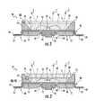
- FIGS. 2 and 3are cross-sectional views of a first embodiment of the light emitter device according to the disclosure herein;
- FIGS. 4A to 4Care views of embodiments of details circled in FIGS. 2 and 3 according to the disclosure herein;
- FIG. 5is a top perspective view of a second embodiment of a light emitter device according to the disclosure herein;
- FIGS. 6 and 7are cross-sectional views of the second embodiment of a light emitter device according to the disclosure herein;
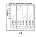
- FIG. 8is a graphical illustration of improved light output for a light emitter device according to the disclosure herein.
- FIG. 9is a graphical illustration of improved light output for light emitter devices according to the disclosure herein.
- references to a structure being formed “on” or “above” another structure or portioncontemplates that additional structure, portion, or both may intervene. References to a structure or a portion being formed “on” another structure or portion without an intervening structure or portion are described herein as being formed “directly on” the structure or portion.
- relative terms such as “on”, “above”, “upper”, “top”, “lower”, or “bottom”are used herein to describe one structure's or portion's relationship to another structure or portion as illustrated in the figures. It will be understood that relative terms such as “on”, “above”, “upper”, “top”, “lower” or “bottom” are intended to encompass different orientations of the device in addition to the orientation depicted in the figures. For example, if the device in the figures is turned over, structure or portion described as “above” other structures or portions would now be oriented “below” the other structures or portions. Likewise, if devices in the figures are rotated along an axis, structure or portion described as “above”, other structures or portions would now be oriented “next to” or “left of” the other structures or portions. Like numbers refer to like elements throughout.
- Light emitter devicescan comprise group III-V nitride (e.g., gallium nitride (GaN)) based light emitting chips such as light emitting diode (LED) chips or lasers that can be fabricated on a growth substrate, for example, a silicon carbide (SiC) substrate, such as those devices manufactured and sold by Cree, Inc. of Durham, N.C.
- a growth substratefor example, a silicon carbide (SiC) substrate, such as those devices manufactured and sold by Cree, Inc. of Durham, N.C.
- Other growth substratesare also contemplated herein, for example and not limited to sapphire, silicon (Si) and GaN.
- SiC substrates/layerscan be 4H polytype silicon carbide substrates/layers.
- SiC candidate polytypessuch as 3C, 6H, and 15 R polytypes, however, can be used.
- Appropriate SiC substratesare available from Cree, Inc., of Durham, N.C., the assignee of the present subject matter, and the methods for producing such substrates are set forth in the scientific literature as well as in a number of commonly assigned U.S. patents, including but not limited to U.S. Pat. No. Re. 34,861; U.S. Pat. No. 4,946,547; and U.S. Pat. No. 5,200,022, the disclosures of which are incorporated by reference herein in their entireties. Any other suitable growth substrates are contemplated herein.
- Group III nitriderefers to those semiconducting compounds formed between nitrogen and one or more elements in Group III of the periodic table, usually aluminum (Al), gallium (Ga), and indium (In).
- the termalso refers to binary, ternary, and quaternary compounds such as GaN, AlGaN and AlInGaN.
- the Group III elementscan combine with nitrogen to form binary (e.g., GaN), ternary (e.g., AlGaN), and quaternary (e.g., AlInGaN) compounds. These compounds may have empirical formulas in which one mole of nitrogen is combined with a total of one mole of the Group III elements. Accordingly, formulas such as AlxGa1-xN where 1>x>0 are often used to describe these compounds. Techniques for epitaxial growth of Group III nitrides have become reasonably well developed and reported in the appropriate scientific literature.
- light emitting chipse.g., LEDs or LED chips
- the crystalline epitaxial growth substrate on which the epitaxial layers comprising an LED chip are growncan be removed, and the freestanding epitaxial layers can be mounted on a substitute carrier substrate or substrate which can have different thermal, electrical, structural and/or optical characteristics than the original substrate.
- the subject matter described hereinis not limited to structures having crystalline epitaxial growth substrates and can be used in connection with structures in which the epitaxial layers have been removed from their original growth substrates and bonded to substitute carrier substrates.
- Group III nitride based chips or LEDscan be fabricated on growth substrates (e.g., Si, SiC, or sapphire substrates) to provide horizontal devices (with at least two electrical contacts on a same side of the LED chip) or vertical devices (with electrical contacts on opposing sides of the LED chip).
- the growth substratecan be maintained on the LED chip after fabrication or removed (e.g., by etching, grinding, polishing, etc.). The growth substrate can be removed, for example, to reduce a thickness of the resulting LED chip and/or to reduce a forward voltage through a vertical LED chip.
- a horizontal device(with or without the growth substrate), for example, can be flip chip bonded (e.g., using solder) to a carrier substrate or printed circuit board (PCB), or wire bonded.
- a vertical device(with or without the growth substrate) can have a first terminal solder bonded to a carrier substrate, mounting pad, or PCB and a second terminal wire bonded to the carrier substrate, electrical element, or PCB. Examples of vertical and horizontal LED chip structures are discussed by way of example in U.S. Publication No. 2008/0258130 to Bergmann et al. and in U.S. Publication No. 2006/0186418 to Edmond et al., the disclosures of which are hereby incorporated by reference herein in their entireties.
- One or more LED chipscan be at least partially coated with one or more phosphors.
- the phosphorscan absorb a portion of light emitted from the LED chip and emit a different wavelength of light such that the light emitter device or package emits a combination of light from each of the LED chip and the phosphor.
- the light emitter device or packageemits what is perceived as white light resulting from a combination of light emission from the LED chip and the phosphor.
- One or more LED chipscan be coated and fabricated using many different methods, with one suitable method being described in U.S. patent application Ser. Nos.
- LED chipscan also be coated using other methods such electrophoretic deposition (EPD), with a suitable EPD method described in U.S. patent application Ser. No. 11/473,089 entitled “Close Loop Electrophoretic Deposition of Semiconductor Devices”, which is also incorporated herein by reference in its entirety. It is understood that light emitter devices, systems, and methods according to the present subject matter can also have multiple LED chips of different colors.
- EPDelectrophoretic deposition
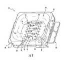
- FIGS. 1 to 4illustrate views of one example of a light emitter package or device generally designated 10 .
- FIGS. 5 to 7illustrate views of another light emitter package or device, generally designated 50 .
- light emitter devices 10 and 50can comprise a surface mount device (SMD) type of emitter package comprising a respective body 12 or submount 52 which can be molded, formed about, or otherwise incorporate components such as electrical leads.
- SMD type light emitter devicescan be suitable for general LED illumination applications, such as indoor and outdoor lighting, automotive lighting, and preferably suitable for high power and/or high brightness lighting applications.
- devices and methods disclosed hereincan exhibit improved chemical and physical resistance to undesirable chemical species and/or physical damage in part by provision of at least one clear barrier layer of material disposed within a cavity of the SMD type device.
- the clear barriercan be adapted to prevent attacks to various device components by harmful chemicals, chemical species, or chemical and/or vaporous complexes, for example, by preventing such components (e.g., Ag or Ag-containing components or substrates) from tarnishing and/or otherwise degrading within the devices.
- devices and methods disclosed hereincan advantageously exhibit improved initial light output and be adapted to maintain such initial light output (e.g., by approximately 95% or more, see FIGS. 8 and 9 ) even in the presence of harmful chemicals, chemical vapors, or complexes by provision of the clear barrier layer 30 ( FIGS. 2 , 6 , 7 ).
- emitter device 10can comprise a body 12 .
- Body 12can be disposed about electrical leads or lead components comprising a thermal element 14 and one or more electrical elements, for example, first and second electrical elements 16 and 18 , respectively. That is, thermal element 14 and electrical elements 16 and 18 can be collectively referred to as a “leads” which can be singulated from a sheet of leadframes (not shown).
- a corner notch, generally designated Ncan be used for indicating electrical polarity of first and second electrical elements 16 and 18 .
- Thermal element 14 and first and second electrical elements 16 and 18can comprise a material that is electrically and/or thermally conductive such as a metal or metal alloy.
- thermal element 14can be electrically and/or thermally isolated from one and/or both of first and second electrical elements 16 and 18 by one or more isolating portions 20 of the body. Thermal element 14 can also be physically separated from electrical elements 16 and 18 via isolating portions 20 of the body.
- One or more LED chips 22can be mounted over thermal element 14 using any suitable die attach technique(s) and/or material(s), for example only and not limited to die attach adhesive (e.g., silicone, epoxy, or conductive silver (Ag) epoxy) or a metal-to-metal die attach technique such as flux or no-flux eutectic, non-eutectic, or thermal compression die attach.
- die attach adhesivee.g., silicone, epoxy, or conductive silver (Ag) epoxy
- metal-to-metal die attach techniquesuch as flux or no-flux eutectic, non-eutectic, or thermal compression die attach.
- LED chips 22can electrically communicate with one and/or both first and second electrical elements 16 and 18 via one or more electrical connectors such as electrically conductive wire bonds 24 .
- LED chips 22can comprise a horizontal device having two electrical contacts (e.g., anode and cathode) on the same side (e.g., upper surface) that can be electrically connected to two electrical elements (e.g., 16 and 18 ) via wire bonds 24 .
- LED chips 22 having one electrical contact on the upper surface that is electrically connected with a single electrical element 16 or 18is also contemplated.
- LED chips 22could comprise a horizontal device having both electrical contacts on the bottom surface, where one contact could be directly attached to first electrical element 16 and the second contact could be directly attached to second electrical element 18 .
- LED chip 22can comprise a horizontally structured chip (e.g., having at least two electrical contacts on a same side of the LED) or a vertically structured chip (e.g., with electrical contacts on opposing sides of the LED) with or without a growth substrate.
- LED chip 22can comprise one or more substantially straight cut and/or beveled (i.e., angled) cut sides or surfaces.
- LED chip 22can comprise a direct attach build (e.g., bonded to a carrier substrate) or a build incorporating a grown substrate such as sapphire, SiC, or GaN.
- LED chips 22can be substantially square or rectangular in shape. LED chips 22 having any build, structure, type, style, shape, and/or dimension are contemplated herein.
- Wire bonds 24 or other electrical attachment connectors and related methodscan be adapted to communicate, transmit, or convey an electrical current or signal from electrical elements 16 and 18 to one or more LED chips 22 thereby causing illumination of the one or more LED chips 22 .
- Thermal element 14 and/or first and second electrical elements 16 and 18can be coated, plated, deposited, or otherwise layered with a reflective material (e.g., 34 of FIGS. 2 , 3 ), such as, for example and without limitation Ag-containing materials such as pure Ag, Ag plate, and/or Ag alloy materials for reflecting light from the one or more LED chips 22 .
- the present subject mattercan improve the chemical resistance of device 10 by incorporating a clear barrier layer 30 ( FIG.
- FIGS. 2 , 3 , 6 , 7serving as a protective barrier or barrier layer disposed over one or more Ag-containing substrates of device 10 , within device 10 , and/or over components of device 10 to prevent contaminants or other material, such as complexes C for illustration purposes ( FIGS. 2 , 3 , 6 , 7 ), from reaching, interacting with, and/or adversely affecting components such as Ag-containing outer portion 34 ( FIGS. 2 , 3 ) of thermal and electrical elements 14 , 16 , and 18 .
- a protective barrier or barrier layerdisposed over one or more Ag-containing substrates of device 10 , within device 10 , and/or over components of device 10 to prevent contaminants or other material, such as complexes C for illustration purposes ( FIGS. 2 , 3 , 6 , 7 ), from reaching, interacting with, and/or adversely affecting components such as Ag-containing outer portion 34 ( FIGS. 2 , 3 ) of thermal and electrical elements 14 , 16 , and 18 .
- LED chips 22 as described hereincan embody a solid state emitter used alone and/or in combination with one or more phosphors or lumiphors to emit light of various colors, color points, or wavelength ranges.
- LED chips 22can comprise chips selected from the following targeted wavelength bins: (1) primarily blue wavelengths (preferably approximately 430 nm to 480 nm; optionally 430-475 nm, 440-475 nm, 450-475 nm, or any suitable sub-range of 430-480 nm); (2) primarily cyan wavelengths (preferably approximately 481 nm to 499 nm); (3) primarily green wavelengths (preferably approximately 500 nm to 570 nm, optionally 505-515 nm, 515-527 nm, or 527-535 nm, or 535-570 nm, or any suitable sub-range of 500-570 nm a or any suitable sub-range of 500-570 nm); (4) primarily yellow wavelengths (preferably approximately 571 to 590
- body 12can comprise any suitable material molded or otherwise disposed about thermal element 14 and/or first and second elements 16 and 18 , respectively.
- body 12can comprise a ceramic material such as a low temperature co-fired ceramic (LTCC) material, a high temperature co-fired ceramic (HTCC) material, alumina, aluminum nitride (AlN), aluminum oxide (Al 2 O 3 ), glass, and/or an Al panel material.
- body 12can comprise a molded plastic material such as polyamide (PA), polyphthalamide (PPA), liquid crystal polymer (LCP), or silicone.
- ESD protection devices 25can optionally be disposed within device 10 and can be electrically connected to electrical elements 16 and 18 and reverse biased with respect to LED chips 22 . Where used, ESD device 25 can protect against damage from ESD within device 10 .
- the arrangement of LED chips 22 and ESD protection device 25allows excessive voltage and/or current passing through light emitter device 10 from an ESD event to pass through protection device 25 instead of LED chips 22 thereby protecting LED chips 22 from damage.
- different elementscan be used as ESD protection devices 25 such as various vertical silicon (Si) Zener diodes, different LEDs arranged reverse biased to LED chips 22 , surface mount varistors and lateral Si diodes.
- ESD device 25can comprise a vertically structured device having one electrical contact on the bottom and another electrical contact on the top; however, horizontally structured devices are also contemplated.
- Body 12 of device 10can comprise a light emission area comprising a space or cavity, generally designated 26 , for example, a reflector cavity optionally coated with a reflective material for reflecting light from the one or more LED chips 22 .
- a light emission areacomprising a space or cavity, generally designated 26 , for example, a reflector cavity optionally coated with a reflective material for reflecting light from the one or more LED chips 22 .
- one or more LED chips 22can be disposed in cavity 26 under a filling material.
- the filling materialcan be at least partially disposed within the cavity 26 or space and over the one or more LED chips 22 .
- Filling materialcan comprise a first discrete layer of filling material, such as an encapsulant layer 28 which can optionally comprise one or more phosphors, lumiphors, and/or phosphoric or lumiphoric materials as denoted by the shaded or speckled appearance.
- Encapsulant layer 28can comprise a layer of silicone encapsulant as known in the art. As silicone can be susceptible to penetration by chemical complexes C ( FIGS. 2 , 3 ), a second discrete layer of material such as clear barrier layer 30 can be arranged over at least a portion of encapsulant layer 28 for improving chemical resistance of device 10 .
- the one or more phosphors disposed in encapsulant layer 28can be adapted to emit light of a desired wavelength when activated by light emitted from the one or more LED chips 22 .
- device 10can emit light having a desired wavelength, color temperature or color point that can be a combination of light emitted from phosphors disposed in encapsulant layer 28 and from the light emitted from one or more LED chips 22 .
- encapsulant layer 28can be adapted for dispensing within cavity 26 .
- At least some of the LED chips 22can be coated with or otherwise disposed to impinge light onto one or more phosphors disposed within encapsulant layer 28 .
- Encapsulant layer 28can be adapted to absorb at least some of the LED chip emissions and responsively emit light of a different wavelength.
- LED chip emissionscan be fully absorbed or only partially absorbed such that emissions from the resulting device include a combination of light from the LED chip 22 and light from one or more phosphors.
- at least one of the LED chips 22can comprise an LED that emits light in the blue wavelength spectrum, with a phosphor absorbing some of the blue light and re-emitting yellow light. The resulting LED chip 22 and phosphor combination may emit a combination of blue and yellow light appearing white or non-white.
- any commercially available yellow phosphorcan be used for white emitting LED chips 22 in devices described herein.
- at least one of the LED chips 22can comprise an LED that emits light in the blue wavelength spectrum and arranged to interact with other phosphors that absorb blue light and emit green light.
- Any commercially available green phosphorcan be used in devices described herein.
- LED chips 22 emitting red lightcan also be provided and used alone and/or in combination with other LED chips 22 for producing warm white light and can comprise LED structures and materials that permit emission of red light directly from the active region of the LED chip 22 (e.g., a phosphide-based active region).
- red emitting LED chips 22can comprise LEDs covered by a phosphor that absorbs the LED light and emits a red light which can combine with other emissions for achieving warm white light. Any combination of LED chip(s) 22 and phosphor(s) wavelength emissions can be used to achieve the desired aggregated spectral output. It is understood that light emitter packages 10 and 50 ( FIGS. 5 to 7 ) as described herein can include multiple LED chips 22 of the same and/or different colors, of which one or more may emit white light or near-white light.
- thermal element 14 and first and second electrical elements 16 and 18can comprise an inner portion 32 and an outer portion 34 .
- inner portion 32 and outer portion 34can comprise electrically and/or thermally conductive materials.
- Outer portion 34may be applied such that it entirely surrounds inner portion 32 as shown, or in other aspects outer portion 34 can optionally plate, coat, or comprise a layer over a single surface or two or more surfaces of portion 32 .
- outer portion 34can comprise a highly reflective Ag-containing substrate or layer of material such as Ag for maximizing light output from device 10 and for assisting in heat dissipation by conducting heat away from the one or more LED chips 22 .
- Outer portion 34can also comprise a substrate containing a Ag alloy instead of pure Ag, and such alloy can contain other metals such as titanium (Ti) or nickel (Ni).
- Inner portion 32can comprise a metal or metal alloy such as copper (Cu) substrate or Cu-alloy substrate.
- an optional layer of material(not shown) can be disposed between inner portion 32 and outer portion 34 , such as a layer of Ni for providing a barrier between the Ag and Cu, thereby preventing defects caused by migratory Cu atoms, such as a defect commonly known as “red plague”.
- outer portion 34can be directly attached to and/or directly coat inner portion 32 .
- Outer portion 34can advantageously reflect light emitted from the one or more LED chips 22 thereby improving optical performance of device 10 .
- Thermal element 14 and electrical elements 16 and 18can be disposed along a floor 36 of cavity 26 such that respective upper surfaces of thermal and electrical elements can be disposed along the same plane and/or different planes.
- upper surfaces of thermal element 14 and electrical elements 16 and 18are disposed along the same plane which is also the plane of floor 36 .
- thermal element 14can be downset such that an upper surface of thermal element 14 can be disposed below floor 36 such that it is below the plane of respective upper surfaces of each electrical element 16 and 18 . That is, thermal element 14 can be downset such that it is disposed on a lower plane than electrical elements 16 and 18 such that thermal element 14 appears sunken in respect to electrical elements 16 and 18 .
- First and second electrical elements 16 and 18can extend internally through body 12 and externally from one or more lateral sides of body 12 and form one or more external tab portions, generally designated 38 and 40 .
- Tab portions 38 and 40can bend to form one or more lower mounting surfaces such that device 10 can be mounted to an underlying substrate.
- Tab portions 38 and 40can outwardly bend away from each other or inwardly bend towards each other thereby adapting either a J-bend or gull-wing orientation as known in the art.
- any configuration of external tabs 38 and 40is contemplated.
- filling material of device 10can comprise a first layer (e.g., encapsulant layer 28 ) and a second discrete and physically separate second layer (e.g., clear barrier layer 30 ).
- first layere.g., encapsulant layer 28
- second discrete layer of materialcan be at least partially disposed above and/or below the encapsulant layer 28 .
- Clear barrier layer 30can be adapted to provide a physical and chemical barrier against harmful chemical complexes generally designated C. As FIGS. 2 and 3 illustrate, harmful chemical complexes C cannot physically penetrate clear barrier layer 30 as indicated by the dotted trajectory lines extending from complexes C, and therefore, cannot degrade components within device 10 disposed below barrier layer 30 .
- clear barrier layer 30can comprise a substantially flat piece of glass that has been cut, trimmed, etched, machined, and/or otherwise physically and dimensionally sized to directly or indirectly cover at least a portion of encapsulant layer 28 .
- barrier layer 30can comprise any type of glass or glass material including but not limited to silica based or silica containing glasses, fluoride containing glasses, aluminosilicates, phosphate containing glasses, borate containing glasses, chalcogenide glasses, glass-ceramic materials, acrylic glasses, polycarbonate materials, polyethylene terephthalate materials, polymer glasses, soda lime glasses, borosilicate glasses, and/or combinations thereof.
- Clear barrier layer 30can, for example and without limitation, comprise a substantially flat, non-domed portion of material that is not primarily useful in curving about chips to focus light. That is, barrier layer 30 can be one that has no or little focusing effect on light passing therethrough such that it is not useful for focusing light as are conventional domed lenses. Instead, barrier layer 30 can provide a physical and chemical barrier thereby protecting device 10 and can actually increase light output by increasing light extraction efficiency.
- glass or “glass material”can comprise any non-crystalline (i.e., amorphous) structure that exhibits a glass transition (i.e., at a glass transition temperature) when heated towards a liquid state.
- the glass transitioni.e., also known as a liquid-glass transition
- Any amorphous solid that exhibits a glass transitioncan, in general, be used to describe a “glass” or “glass material” as used herein.
- clear barrier layer 30can also be adapted to improve light output by increasing light extraction efficiency.
- addition of clear barrier layer 30 within device 10can improve the light output of device 10 (e.g., improve the luminous flux) by approximately 1% or more (e.g., see FIG. 8 ). In other aspects, addition of clear barrier layer 30 within device 10 can improve the luminous flux by approximately 2% or more, and even by approximately 5% or more.
- Clear barrier layer 30can have any suitable thickness. For example and without limitation, the thickness of clear barrier layer 30 can be approximately 0.1 mm or greater. In one aspect, the thickness of clear barrier layer 30 can be approximately 0.6 mm or greater. In another aspect, the thickness of clear barrier layer 30 can be approximately 0.6 mm or less. In a further aspect, the thickness of clear barrier layer 30 can be from approximately 0.8 mm to 5 mm.
- clear barrier layer 30can, for example and without limitation, comprise anywhere from approximately 1 to 70% or more of a total encapsulant volume or a total cavity 26 volume, depending upon the package and thickness used. In one aspect, clear barrier layer 30 can comprise a range of between approximately 5 and 50% of a total cavity 26 volume.
- device 10can comprise an overall thickness of approximately 2 mm, with clear barrier layer 30 comprising a thickness of approximately 0.6, thus, approximately a 30% by volume ratio.
- device 10can comprise a clear barrier layer 30 having a thickness of approximately 0.1 mm or greater.
- Device 10can comprise an overall thickness of approximately 2.0 mm or less or approximately 2.0 mm or greater. In one aspect, device 10 can comprise an overall thickness of approximately 1.5 mm or greater.
- Device 10can comprise a ratio of thickness of clear barrier layer 30 to thickness of the light emitter device 10 that is approximately 25% or greater.
- the ratio of thickness of clear barrier layer 30 to thickness of the light emitter device 10can also be approximately 30%.
- device 10can comprise a ratio of thickness of clear barrier layer 30 to thickness of light emitter device 10 that is approximately 25% or less.
- clear barrier layer 30can be directly disposed over one or more portions of encapsulant layer 28 .
- clear barrier layer 30can be disposed between one or more encapsulant layers 28 .
- Clear barrier layer 30can for example be applied during or after application of encapsulant layer 28 to provide a physical and chemical barrier between the outside environment and Ag-containing substrates or components such as outer portion 34 of thermal/electrical components or elements.
- FIGS. 6 and 7illustrate various other alternative locations and/or arrangements of clear barrier layer 30 in a SMD type package or device for providing protection against chemical complexes C and against physical damage to components within the device.
- undesired chemicals, vapors, or complexes Ccan comprise chemical vapors containing sulfur, sulfur containing compounds (sulfides, sulfites, sulfates, SO x ), chlorine or bromine containing complexes, nitric oxide or nitrogen dioxide (NO x ), and/or oxidizing organic vapor compounds.
- Complexes Ccan degrade the Ag components (e.g., outer portion 34 of thermal/electrical elements) and result in a loss of brightness output and noticeable darkening of surfaces within the device.
- Clear barrier layer 30can improve the chemical resistance of device 10 and components within device 10 such that harmful vapors, chemicals, or complexes C cannot reach Ag-containing components (e.g., outer portion 34 ) as illustrated by the dotted trajectory of complexes C being repelled from the surface of clear barrier layer 30 , thereby minimizing the damage to reflective Ag components, and further minimizing and/or totally preventing any loss in brightness from device 10 and/or darkening of components within device 10 .
- Ag-containing componentse.g., outer portion 34
- clear barrier layer 30can be selectively applied at or in parallel with any number of processing steps within the manufacturing process (e.g., before/during/after encapsulation) for providing broad protection against chemical vapors, such as but not limited to, nitric oxide or nitrogen dioxide (NO x ), oxidizing organic vapor compounds, sulfur, sulfur-containing compounds (e.g., sulfides, sulfates, SO x ) and chlorine- or bromine-containing complexes.
- chemical vaporssuch as but not limited to, nitric oxide or nitrogen dioxide (NO x )
- SO xsulfur-containing compounds
- chlorine- or bromine-containing complexessuch as but not limited to, chlorine- or bromine-containing complexes.
- devices described hereincan exhibit excellent chemical, including sulfur, resistance and long lasting protection against chemical complexes C as compared to conventional devices.
- device 10can retain approximately 95% or more of its initial brightness value (e.g., measured in lumens, see FIG. 9 ) when exposed to a sulfur environment as compared to conventional devices which may only retain approximately 70% of its initial brightness value when exposed to the same sulfur environment.
- an improved devicesuch as device 10 can retain approximately 100% of its initial brightness value.
- clear barrier layer 30can be disposed above a single encapsulant layer 28 as shown.
- Clear barrier layer 30can be, but does not have to be substantially the same length and width dimension and/or the same geometry as underlying encapsulant layer 28 .
- an embodiment where clear barrier layer 30 is the same or substantially the same as encapsulant layer 28may be preferred as encapsulant layer 28 can be fully covered by layer 30 and can be better protected against permeation by harmful chemical complexes C. As the detailed view in FIG.
- a thin layer of silicone encapsulant and/or other materialcan be applied along edges of clear barrier layer 30 thereby forming a fillet or fillet member (e.g., 44 , see FIG. 4A ) to improve adhesion of layer 30 within device 10 .
- the fillet 44( FIG. 4A ) can be disposed between portions of clear barrier layer 30 and body 12 of device and can act as glue for holding clear barrier layer 30 in place.
- Such layer or filletis optional.
- clear barrier layer 30can also be disposed between more than one encapsulant layer 28 .
- clear barrier layer 30can be disposed between a first encapsulant layer 28 and a second encapsulant layer 28 for preventing chemical complexes from reaching vulnerable components (e.g., Ag-containing portion 34 of electrical elements 16 and 18 ) within device 10 .
- Clear barrier layer 30can also be disposed between one or more encapsulant layers 28 , where at least one of the layers does not contain phosphors or lumiphors (e.g., an optically clear encapsulant layer 80 , see FIG. 7 ).
- Clear barrier layer 30can comprise any suitable material that is optically clear and adapted to provide a solid, non-crystalline structure capable of providing a chemical and physical barrier when placed over encapsulant layer 28 .
- clear barrier layer 30can comprise a glass or glass material such as silica based or silica containing glasses, fluoride glasses, aluminosilicates, phosphate glasses, borate glasses, chalcogenide glasses, glass-ceramic materials, acrylic glasses, polycarbonate materials, polyethylene terephthalate materials, polymer glasses, soda lime glasses, borosilicate glasses, and/or combinations thereof which can be placed within one or more walls of the light emission area or cavity 26 .
- a glass or glass materialsuch as silica based or silica containing glasses, fluoride glasses, aluminosilicates, phosphate glasses, borate glasses, chalcogenide glasses, glass-ceramic materials, acrylic glasses, polycarbonate materials, polyethylene terephthalate materials, polymer glasses, soda lime glasses, borosilicate glasses, and/or combinations thereof which can be placed within one or more walls of the light emission area or cavity 26 .
- clear barrier layer 30can comprise a layer of material that is not molded or dispensed and that can be physically shaped via cutting, trimming, machining, etching, etc. and adapted to fit over and completely or substantially cover encapsulant layer 28 .
- Clear barrier layer 30can comprise a layer of material that does not contain phosphoric or lumiphoric materials therein, but can optionally be coated with phosphoric material and/or any other desired coating, such as diffusers, reflectors and/or anti-reflection layers that may optionally affect light emission and/or reflection.
- clear barrier layer 30can comprise a material adapted to protect device 10 against attack from chemical complexes C, but it can also advantageously provide general physical protection of device as well.
- clear barrier layer 30can provide general physical protection of LED chips 22 and wirebonds 24 from physical damage that may potentially result from physical penetration of encapsulant layer 28 .
- clear barrier layer 30can advantageously improve chemical and physical resistance of device 10 .
- clear barrier layer 30(and/or encapsulant layer 28 depending upon which layer is on top) can be partially disposed below and/or above an upper surface 42 of device 10 .
- filling materialcan comprise clear barrier layer 30 disposed above encapsulant layer 28 where clear layer is flush or substantially flush with upper surface 42 of device as shown. That is, clear barrier layer 30 can be substantially flush with and disposed along the same plane as upper surface 42 of device 10 .
- filling materialcan comprise encapsulant layer 28 disposed above clear barrier layer 30 where encapsulant layer 28 of filling material can be filled to a level flush with upper surface 42 of device. Clear barrier layer 30 can be at least partially disposed below upper surface 42 .
- clear barrier layer 30can be entirely disposed below upper surface 42 of device.
- the encapsulant layer 28can be filled such that it forms a concave or convex surface with respect to upper surface 42 of device 10 .
- clear barrier layer 30comprises a physical glass or plastic barrier, it can comprise substantially flat (i.e., non-domed) surfaces whether disposed above and/or below upper surface 42 .
- clear barrier layer 30is preferably disposed above LED chips 22 and respective wire bonds 24 .
- a first layer of materiale.g., encapsulant 28 with or without phosphors
- a second layer of materiale.g., a subsequent encapsulant layer 28
- the second layer of materiale.g., a subsequent encapsulant layer 28
- second encapsulant layer 28can be sequentially dispensed within cavity 26 over first encapsulant layer 28 and after placement of clear barrier layer 30 such that the separately dispensed encapsulant layers can be cured at the same time. That is, multiple dispense and multiple curing steps (i.e., separately dispensing and curing of encapsulant layers 28 ) are contemplated herein, or multiple dispense and one curing step (i.e., separately dispensing and simultaneous curing of encapsulant layers 28 ) are contemplated herein.
- clear barrier layer 30can be directly disposed adjacent at least one encapsulant layer 28 and/or over a portion of at least one encapsulant layer.
- the various devices shown and described hereincan comprise the additional, discrete clear barrier layer 30 that can be physically separate and a different material than one or more encapsulant layer(s) 28 for improving chemical and physical resistance as well as light output or brightness of device 10 .
- FIG. 4Ais a close up view of the detail circled in FIG. 2 .
- FIGS. 4B and 4Care close up views of the detail circled in FIG. 3 .
- FIG. 4Aillustrates a clear and/or reflective fillet generally designated 44 which can be placed or dispensed over clear barrier later 30 for improving adhesion of layer 30 within device 10 .
- Fillet 44can comprise a layer of clear silicone encapsulant or other dispensable material and can be adapted to secure and/or “glue” clear barrier layer 30 within device 10 .
- FIGS. 4B and 4Cillustrate further embodiments operable to retain clear barrier layer 30 in device 10 .
- clear barrier layer 30can simply be cut, trimmed, machined, and/or otherwise sized and configured such that it is substantially the same size as inner walls of cavity 26 such that clear barrier layer 30 can simply be positioned over and float over encapsulant 28 as illustrated in FIGS. 2 and 3 . That is, the retaining members in FIGS. 4A to 4C may not be required, and are therefore optional.
- device 10can comprise a notch, generally designated 46 , adapted to receive a portion of clear barrier layer 30 . That is, one or more notches 46 can be formed in sidewalls of cavity 26 such that clear barrier layer 30 can extend or be inset between one or more portions of body 12 . In one aspect, clear barrier layer 30 can be at least partially disposed within body 12 when inset in notch 46 . As FIG. 4C illustrates, in one aspect a portion of body 12 can be adapted to protrude from a sidewall of cavity 26 such that clear barrier layer 30 can rest over the protruding or projecting portion, generally designated 48 .
- projecting portion 48can comprise a small, miniscule dimension such that it does not interfere with and/or block light emitted from LED chips 22 . More than one projecting portions 48 can be disposed or spaced about wall(s) of cavity 26 at substantially the same height such that clear barrier layer 30 can be positioned substantially flat within device 10 . As illustrated in FIGS. 2 and 3 , outermost exterior or lateral walls of clear barrier layer 30 can optionally comprise beveled or angled sides for fitting substantially flush against inner walls of cavity 26 .
- one or more additional processing techniques or stepscan optionally be performed during manufacture of devices described herein for improving adhesion between one or more layers within the devices.
- Such optionally processing stepscan be used and applied to devices previously shown and described, as well as device 50 shown and described in FIGS. 5 through 7 hereinbelow.
- such optional techniquescan be performed to one or more surfaces of underlying encapsulant layer 28 , clear barrier layer 30 , and/or clear encapsulant 80 ( FIG. 7 ) prior to deposition or application of one or more subsequent surfaces or layers within a device.
- one or more of these surfacescan be physically, chemically, or thermally prepared or treated to improve adhesion between the treated surface and adjacent surface(s) or adjacent layer(s).
- Optional processing steps that are physical in naturecan comprise, for example and without limitation, sandblasting, plasma etching, brushing, lapping, sanding, burnishing, grinding, and/or any suitable form of surface roughening (e.g., physically texturizing the surface) to improve adhesion between one or more layers or surfaces within devices shown and described herein.
- Optional processing steps that are chemical in naturecan comprise, for example and without limitation, chemical etching, applying solvents, applying organic solvents, applying acids, applying bases, vapor degreasing, priming, or any suitable chemically process for treating a surface to improve adhesion between one or more layers or surfaces within devices shown and described herein.
- Optional thermal processing stepscan comprise, without limitation, prebaking, preheating, or any suitable thermal treatment that improves adhesion between one or more layers or surfaces within devices shown and described herein.
- FIGS. 5 to 7illustrate top perspective and cross-sectional views of another embodiment of a light emitter package or device, generally designated 50 .
- Light emitter device 50can also incorporate an optically clear barrier layer 30 ( FIGS. 6 , 7 ) that is physically separate or discrete from an encapsulant layer 28 which can optionally contain phosphor.
- barrier layer 30can advantageously improve chemical and physical resistance of device 50 by serving as a physical and chemical barrier against harmful chemical complexes C and/or physical damage when chemical or physical components permeate encapsulant layer 28 .
- Clear barrier layer 30can also improve light output or brightness of device 50 .
- Light emitter device 50can comprise an SMD type package, similar to device 10 .
- Light emitter device 50can comprise a submount 52 over which a light emission area, generally designated 54 , can be disposed.
- Light emission area 54can comprise a cavity or space in which one or more LED chips 22 can be disposed under at least a first layer of filling material, such as an encapsulant layer 28 (see FIGS. 6 , 7 ).
- LED chips 22can comprise a plurality of chips adapted to emit the same color or targeted wavelength of light, or at least one of the plurality of LED chips 22 can be adapted to emit light that is a different color (e.g., from a different targeted wavelength bin) than a second LED of the plurality of LED chips 22 .
- a single LED chip 22is contemplated for use in emitter devices described herein.
- LED chips 22can be configured to emit light having wavelengths in the visible spectrum portion of the electromagnetic spectrum in any of the previously described colors and/or wavelength ranges.
- encapsulant layer 28can comprise phosphors adapted to emit light in any color, for example, yellow, green, and/or red when activated by emissions from the one or more LED chips 22 . Any combination of LED chip 22 and phosphor colors or targeted wavelength ranges are contemplated herein for producing white light, cool white light, and/or warm white light.
- emission area 54can be substantially centrally disposed with respect to submount 52 of light emitter device 50 .
- emission area 54can be disposed at any location over light emitter device 50 , for example, in a corner or adjacent an edge. Any location is contemplated, and more than one emission area 54 is also contemplated. For illustration purposes, a single, circular emission area 54 is shown; however, the number, size, shape, and/or location of emission area 54 can change subject to the discretion of light emitter device consumers, manufacturers, and/or designers. Emission area 54 can comprise any suitable shape such as a substantially circular, square, oval, rectangular, diamond, irregular, regular, or asymmetrical shape.
- Light emitter device 50can further comprise a retention material 56 at least partially disposed about emission area 54 where retention material 56 can be referred to as a dam.
- Retention material 56can comprise any material such as a silicone, ceramic, thermoplastic, and/or thermosetting polymer material.
- retention material 56is adapted for dispensing about emission area 54 , which can be advantageous as it is easy to apply and easy to obtain any desired size and/or shape.
- Submount 52can comprise any suitable mounting substrate, for example, a printed circuit board (PCB), a metal core printed circuit board (MCPCB), an external circuit, a dielectric laminate panel, a ceramic panel, an Al panel, AlN, Al 2 O 3 , or any other suitable substrate over which lighting devices such as LED chips may mount and/or attach.
- LED chips 22 disposed in emission area 54can electrically and/or thermally communicate with electrical elements disposed with submount 52 , for example, electrically conductive traces (e.g., 64 , 66 of FIGS. 6 , 7 ).
- Emission area 54can comprise a single and/or a plurality of LED chips 22 disposed within and/or below encapsulant layer 28 such as illustrated in FIG. 6 .
- a first layer of reflecting material 68can be disposed between portions of submount 52 and LED chips 22 .
- layer 68can comprise a layer of reflective Ag-containing material such as pure Ag or a Ag-alloy material for maximizing brightness of light emitted from light emitter device 50 .
- emission area 54 of light emitter device 50can comprise more than one layer of filling material, where at least one layer is configured to prevent tarnishing or degradation of Ag-containing components, for example, layer 68 .
- Emission area 54can comprise a first layer of phosphor containing encapsulant 28 as denoted by the shaded or speckled appearance, and a second optically transparent or clear barrier layer 30 adapted to improve chemical and physical resistance.
- Emission area 54can comprise a second layer of filling material at least partially disposed above and/or below the phosphor containing encapsulant layer 28 .
- the second layer of filling materialcan comprise clear barrier layer 30 ( FIGS. 6 , 7 ) of material adapted to improve light output by increasing light extraction efficiency.
- clear barrier layer 30can comprise a substantially flat piece of glass or glass material including but not limited to silica based or silica containing glasses, fluoride containing glasses, aluminosilicates, phosphate containing glasses, borate containing glasses, chalcogenide glasses, glass-ceramic materials, acrylic glasses, polycarbonate materials, polyethylene terephthalate materials, polymer glasses, soda lime glasses, borosilicate glasses, and/or combinations thereof.
- clear barrier layer 30can comprise any other solid non-crystalline material and preferably optically clear material that has been cut and/or dimensionally sized to cover encapsulant layer 28 .
- clear barrier layer 30can also be adapted to improve light output by increasing light extraction efficiency.
- addition of clear barrier layer 30 within device 50can improve the luminous flux by approximately 1% or more (e.g., see FIG. 8 . In other aspects, addition of clear barrier layer 30 within device 50 can improve the luminous flux by approximately 2% or more, and even by approximately 5% or more.
- LED chips 22can comprise any suitable size and/or shape of chip and can be vertically structured (e.g., electrical contacts on opposing sides) and/or horizontally structured (e.g., contacts on the same side or surface).
- LED chips 22can comprise any style of chip for example, straight cut and/or bevel cut chips, a sapphire, SiC, or GaN growth substrate or no substrate.
- One or more LED chips 22can form a multi-chip array of LED chips 22 electrically connected to each other and/or electrically conductive traces in combinations of series and parallel configurations.
- LED chips 22can be arranged in one or more strings of LED chips, where each string can comprise more than one LED chip electrically connected in series.
- Strings of LED chips 22can be electrically connected in parallel to other strings of LED chips 22 .
- Strings of LED chips 22can be arranged in one or more pattern (not shown).
- LED chips 22can be electrically connected to other LEDs in series, parallel, and/or combinations of series and parallel arrangements depending upon the application.
- light emitter device 50can further comprise at least one opening or hole, generally designated 58 , that can be disposed through or at least partially through submount 52 for facilitating attachment of light emitter device 50 to an external substrate, circuit, or surface.
- at least one holecan be disposed through or at least partially through submount 52 for facilitating attachment of light emitter device 50 to an external substrate, circuit, or surface.
- one or more screwscan be inserted through the at least one hole 58 for securing device 50 to another member, structure, or substrate.
- Light emitter device 50can also comprise one or more electrical attachment surfaces 60 .
- attachment surfaces 60comprise electrical contacts such as solder contacts or connectors.
- Attachment surfaces 60can be any suitable configuration, size, shape and/or location and can comprise positive and negative electrode terminals, denoted by the “+” and/or “ ⁇ ” signs on respective sides of device 50 , through which an electrical current or signal can pass when connected to an external power source.
- attachment surfaces 60can comprise devices configured to clamp, crimp, or otherwise attach to external wires (not shown). Electrical current or signal can pass into light emitter device 50 from the external wires electrically connected to device 50 at the attachment surfaces 60 . Electrical current can flow into the emission area 54 to facilitate light output from the LED chips 22 disposed therein ( FIGS. 6 , 7 ). Attachment surfaces 60 can electrically communicate with LED chips 22 of emission area 54 via conductive traces 64 and 66 ( FIGS. 6 , 7 ).
- attachment surfaces 60can comprise a same layer of material as first and second conductive traces 64 and 66 ( FIGS. 6 , 7 ) and therefore can electrically communicate to LED chips 22 attached to traces 64 and 66 via electrical connectors such as wire bonds 24 .
- Electrical connectorscan comprise wire bonds 24 or other suitable members for electrically connecting LED chips 22 to first and second conductive traces 64 and 66 ( FIGS. 6 , 7 ). That is, in one aspect LED chips 22 ( FIGS.
- LED chips 22can comprise horizontally structured devices having both electrical contacts (e.g., anode and cathode) on the same top surface of respective LED chip 22 such that the contacts (e.g., bond pads) can electrically connect with traces (e.g., 64 and 66 , FIGS. 6 , 7 ) via wire bonds 24 .
- LED chips 22can comprise horizontal devices having both electrical contacts (e.g., anode and cathode) on a bottom surface such that wire bonds 24 are unnecessary.
- LED chips 22can comprise vertical devices having electrical contacts on opposing sides such that one wire bond 24 is needed. Any type or structure of LED chip 22 is contemplated herein.
- the first layer of filling materialcan comprise an encapsulant layer 28 that can be disposed between inner walls of retention material 56 .
- Encapsulant layer 28can comprise a predetermined, or selective, amount of one or more phosphors and/or lumiphors in an amount suitable for any desired light emission, for example, suitable for white light conversion or any given color temperature or color point.
- Encapsulant layer 28can comprise a silicone encapsulant material, such as a phenyl or methyl silicone having the one or more phosphors disposed therein.
- Encapsulant layer 28can interact with light emitted from the plurality of LED chips 22 such that a perceived white light, or any suitable and/or desirable wavelength of light, can be observed.
- Retention material 56can be adapted for dispensing, positioning, damming, or placing, about at least a portion of emission area 54 .
- light emitter device 50can further comprise at least a second layer of filling material at least partially disposed above and/or below the phosphor containing encapsulant layer 28 .
- the second layer of filling materialcan comprise a discrete layer of the previously described optically clear barrier layer 30 of material adapted to improve chemical and physical resistance of device 50 as well as improve light output by increasing light extraction efficiency.
- a single clear barrier layer 30can be disposed above a single encapsulant layer 28 as shown, however, and/or more than one encapsulant layer 28 (e.g., FIG. 3 ) and one or more clear encapsulant layers (e.g., 80 , FIG. 7 ) are contemplated herein.
- Clear barrier layer 30can comprise any suitable material having substantially flat upper and lower surfaces (i.e., flat surfaces disposed adjacent encapsulant layer 28 ) and can be physically solid in its initial and final forms (e.g., not dispensed).
- filling material comprised of encapsulant and clear barrier layer 30can be substantially flush with an upper surface of device 50 , that is, an upper surface of retention material 56 .
- clear barrier layer 30can be substantially flush with and disposed along a same plane of upper surface of device 50 (i.e., substantially flush with and/or disposed along the same plane as upper surface of retention material 56 ).
- Clear barrier layer 30can be at least partially disposed below upper surface of device (e.g., partially disposed below upper surface of retention material 56 ).
- clear barrier layer 30can be entirely disposed below upper surface of device (e.g., entirely disposed below upper surface of retention material 56 ).
- Clear barrier layer 30can be physically manipulated via cutting, trimming, etching, machining and/or otherwise sized to fit within emission area 54 .
- clear barrier layer 30fits flush against walls of retention material 56 and preferably is the same length and width dimension and the same geometry as encapsulant layer 28 .
- Clear barrier layer 30can be thicker and/or thinner than encapsulant layer 28 .
- Clear barrier layer 30can optionally be coated with phosphoric or lumiphoric materials or any other optical film (not shown).
- clear barrier layer 30can comprise a layer of glass, plastic, polymer, or ceramic material configured to conform in size to fit substantially between one or more walls of retention material 56 .
- clear barrier layer 30can prevent harmful chemical complexes C from penetrating one or more layers of encapsulant as indicated by the dotted trajectory lines associated with chemical complexes C.
- clear barrier layer 30can advantageously prevent physical damage from occurring to LED chips 22 and/or wirebonds 24 within emission area 54 by improving physical resistance of emission area 54 .
- addition of clear barrier layer 30 alonecan contribute to improved light output of light emitter device 10 by increasing the overall luminous output of device 50 .
- phosphor containing encapsulant layer 28 or a clear encapsulante.g., 80 , FIG. 7
- Clear barrier layer 30can be placed over encapsulant layer 28 , between encapsulant layers 28 , and/or between an encapsulant layer 28 and/or clear encapsulant 80 ( FIG. 7 ) and can optionally comprise curved and/or angled sidewalls to substantially fit flush against inner walls of retention material 56 .
- a layer of clear encapsulant 80can optionally be disposed within light emission area 54 either above and/or below clear barrier layer 30 .
- Clear encapsulant 80can comprise a layer of methyl or phenyl silicone encapsulant through which chemical complexes C may permeate.
- clear barrier layer 30can be positioned directly on or over portions of clear encapsulant 80 , between one or more portions or layers of clear encapsulant 80 , and/or between portions of encapsulant layer 28 and clear encapsulant 80 to prevent such complexes C from damaging Ag or Ag-containing components (e.g., Ag-containing layer 68 ).
- encapsulant layer 28is illustrated as comprising the first layer dispensed over LED chips 22 and respective wire bonds 24
- clear barrier layer 30is illustrated as comprising the second or intervening layer
- clear encapsulant 80is illustrated as comprising the third layer.
- any suitable combination, location, or placement of encapsulant layer 28 , clear barrier layer 30 , and clear encapsulant 80is contemplated herein.
- the uppermost layer, for example, clear encapsulant 80can be filled to any level within walls of emission area 54 and can be the same thickness as encapsulant layer 28 or thicker or thinner than encapsulant layer 28 .
- clear encapsulant and/orcan be filled to a level substantially flush with an upper surface device 50 , for example, an upper surface of retention material 56 .
- clear encapsulant 80can be disposed below clear barrier layer 30 and encapsulant layer 28 could be disposed over clear barrier layer 30 .
- clear encapsulant 80can be directly adjacent to one or more portions of encapsulant layer 28 . More than one layer of clear encapsulant 80 is contemplated herein.
- the first deposited layer(e.g., either encapsulant layer 28 or clear encapsulant 80 ) can be deposited in emission area 54 first and cured prior to dispensing a subsequent layer (e.g., another encapsulant layer 28 or clear barrier layer 30 ) such that the subsequently deposited layer can undergo a separate curing step.
- a subsequent layere.g., another encapsulant layer 28 or clear barrier layer 30
- encapsulant layer 28 and clear barrier layer 30can be sequentially dispensed in emission area 54 , either both before placement of clear barrier layer 30 and/or such that clear barrier layer 30 is positioned therebetween such that encapsulant layer 28 and clear encapsulant 80 can be cured at the same time.
- multiple dispense and multiple curing stepsi.e., separately dispensing and curing of encapsulant layer 28 and clear encapsulant 80
- multiple dispense steps and one curing stepi.e., separately dispensing and simultaneous curing of encapsulant layer 28 and clear encapsulant 80
- can be usedmultiple dispense steps and one curing step
- FIGS. 6 and 7further illustrate retention material 56 dispensed or otherwise placed over submount 52 after wire bonding the one or more LED chips 22 such that retention material 56 is disposed over and at least partially covers at least a portion of the wire bonds 24 .
- wire bonds 24 of the outermost edge LED chips in a given set or string of LED chips 22can be disposed within retention material 14 .
- devicecan contain many strings of LED chips 22 of any number, for example, less than four or more than four LED chips 22 can be electrically connected in series, parallel, and/or combinations of series and parallel arrangements.
- Strings of LED chips 22can comprise diodes of the same and/or different colors, or wavelength bins, and different colors of phosphors can be used in the encapsulant layer 28 disposed over LED chips 22 that are the same or different colors in order to achieve emitted light of a desired color temperature or color point.
- LED chips 22can attach to a conductive pad 70 or intervening layers (e.g., layer 68 described below) disposed between LED chip 22 and conductive pad 70 using any die attach technique or materials as known in art and mentioned above, for example adhesive attach, metal or silicone epoxy attach, solder attach, flux-attach, or direct metal-to-metal die attach techniques and materials as known in the art.
- LED chips 22can be arranged, disposed, or mounted over an electrically and/or thermally conductive pad 70 .
- Conductive pad 70can be electrically and/or thermally conductive and can comprise any suitable electrically and/or thermally conducting material.
- conductive pad 70comprises a layer of Cu or a Cu substrate.
- LED chips 22can be electrically connected to first and second conductive traces 64 and 66 via optional wire bonds 24 .
- One of first and second conductive traces 64 and 66can comprise an anode and the other a cathode.
- Conductive traces 64 and 66can also comprise a layer of electrically conductive Cu or Cu substrate.
- conductive pad 70 and traces 64 and 66can comprise the same Cu substrate from which traces 64 and 66 have been singulated or separated from pad 70 via etching or other removal method.
- solder mask 72can be applied such that it is at least partially disposed between conductive pad 70 and respective conductive traces 64 and 66 .
- Solder mask 72can comprise a white material for reflecting light from light emitter device 50 .
- One or more layers of materialcan be disposed between LED chips 22 and conductive pad 70 .
- one or more layers of materialcan be disposed over conductive traces 64 and 66 .
- a first intervening layer or substrate of material 68can be disposed between LED chips 22 and conductive pad 70 and disposed over traces 64 and 66 .
- First layer of material 68can comprise a layer of reflective Ag or Ag-alloy material for maximizing brightness of light emitted from light emitter device 50 .
- first layer of material 68can comprise a Ag or Ag-containing substrate adapted to increase brightness of device 50 .
- One or more additional layers of materialcan be disposed between first layer 68 and conductive pad 70 and/or first layer 68 and traces 64 and 66 , for example, a layer of Ni can be disposed therebetween for providing a barrier between the Cu of pad and traces 70 , 64 , and 66 and the Ag of layer 68 .
- clear barrier layer Ccan prevent physical and/or chemical damage from occurring to Ag or Ag-containing substrates (e.g., layer 68 ) disposed within device 50 thereby improving physical and chemical resistance of device 50 .
- FIGS. 6 and 7further illustrate a cross-section of submount 52 over which LED chips 22 can be mounted or otherwise arranged.
- Submount 52can comprise, for example, conductive pad 70 , first and second conductive traces 64 and 66 , and solder mask 72 at least partially disposed between conductive pad 70 and each of conductive traces 64 and/or 66 .
- Conductive traces 64 , 66 and conductive pad 70can be coated with a first layer 68 , for example a Ag or Ag-containing layer.
- Submount 52can further comprise a dielectric layer 74 , and a core layer 76 .
- solder mask 72can directly adhere to portions of dielectric layer 74 .
- submount 52can comprise a MCPCB, for example, those available and manufactured by The Bergquist Company of Chanhassan, Minn. Any suitable submount 52 can be used, however.
- Core layer 76can comprise a conductive metal layer, for example copper or aluminum.
- Dielectric layer 74can comprise an electrically insulating but thermally conductive material to assist with heat dissipation through submount 52 .
- device 50can comprise a package which does not require or use any secondary optics to keep harmful elements from degrading conductive pad 70 .
- devices, components and methods disclosed hereinprovide for improved chemical resistance and improved chemical properties where zero or minimum loss of brightness occurs, even in the presence of harmful chemicals and can be applicable to any SMD type device or multi-array device disclosed herein. Such improvements can prevent Ag coated components from tarnishing, darkening, corroding, or otherwise degrading.
- FIG. 8illustrates increases in light output for devices described herein and compares devices which do not have a clear barrier layer 30 (i.e., groups labeled “NO BARRIER”) with devices which implement or integrate a clear barrier layer 30 (i.e., groups labeled “WITH BARRIER”).
- Devices testedincluded SMD type packages (e.g., devices 10 or 50 ) as described herein comprising a clear barrier layer 30 of soda lime glass placed over encapsulant layer 28 (e.g., FIG. 6 ).
- SMD type packagese.g., devices 10 or 50
- FIG. 8illustrates, luminous flux, or brightness devices comprising an approximately 4000K normal white color temperature can increase by more than approximately 1% when a clear barrier layer 30 is implemented within the device.
- clear barrier layer 30increased luminous flux by approximately 1.5% or more (e.g., such as the approximately increase from approximately 1040 lumens (lm) to approximately 1060 lm).
- increases in light output of more than approximately 1.5% and even more than approximately 5%are contemplated.
- the improved devices disclosed hereini.e., within the group “WITH BARRIER” can comprise a light output of approximately 1160 to 1190 lm as compared to devices without a barrier which comprise a light output of approximately 1140 lm.
- the luminous flux values obtained for FIG. 8were measured at 270 mA.
- FIG. 9is a graphical illustration of brightness levels, or light output, of devices after exposure to a sulfur environment.
- improved devicescomprising a clear barrier layer 30 (e.g., group labeled “WITH BARRIER”) were measured before exposure to a sulfur environment and after exposure to a sulfur environment.
- the improved devicesretained approximately 95% of initial brightness levels after exposure to a sulfur environment.
- Devices which did not have a barrier layer onlye.g., group labeled “WITHOUT” retained approximately 70% of brightness levels after exposure to the sulfur environment.
- the significant loss in brightnesscan be attributed in part to the darkening or tarnishing of the Ag or Ag-containing components within the emitter device when exposed to a sulfur containing environment (i.e., when sulfur penetrates the silicone encapsulant layer).
- clear barrier layer 30can improve the resistance of device by preventing tarnishing or darkening of Ag-containing components when exposed to harmful chemical complexes, such as sulfur containing vapors or chemical complexes.
- Embodiments of the present disclosure shown in the drawings and described aboveare exemplary of numerous embodiments that can be made within the scope of the appended claims.
- Devices, components, and methods described hereincan advantageously improve chemical resistance to undesirable chemicals and/or chemical vapors within encapsulated emitter devices, while promoting ease of manufacture and increasing device reliability and performance in high power and/or high brightness applications. Described methods can be used and applied to create chemically resistant surface mount device (SMD) type of emitter devices of any size, thickness, and/or dimension.
- SMDsurface mount device
- Devices and methods described hereincan advantageously be used and adapted within any style of emitter device, for example, devices including a single LED chip, multiple chips, and/or multi-arrays of LED chips.
- Devices and methods described hereincan also advantageously be used and adapted for use with various body or submount materials such as plastic, ceramic, glass, aluminum nitride (AlN), aluminum oxide (Al 2 O 3 ), printed circuit board (PCB), metal core printed circuit board (MCPCB), and aluminum panel based devices. It is contemplated that the configurations of light emitter devices having improved light output and related methods can comprise numerous configurations other than those specifically disclosed, including combinations of those specifically disclosed.
Landscapes
- Led Device Packages (AREA)
Abstract
Description
- This application is a continuation-in-part of and claims priority to both U.S. patent application Ser. No. 13/372,063, filed Feb. 13, 2012, and U.S. patent application Ser. No. 13/372,076, filed Feb. 13, 2012, the disclosures of which are incorporated by reference herein in their entireties.
- The subject matter herein relates generally to light emitter devices and related methods. More particularly, the subject matter herein relates to light emitter devices having improved chemical and physical resistance and related methods.
- Light emitting diodes (LEDs) can be utilized in light emitter devices or packages for providing white light (e.g., perceived as being white or near-white), and they are developing as replacements for incandescent, fluorescent, and metal halide high-intensity discharge (HID) light products. Conventional emitter devices or packages can incorporate components such as metallic traces or mounting surfaces which can become tarnished, corroded, or otherwise degraded when exposed to various undesirable chemicals and/or chemical vapors. Such chemicals and/or chemical vapors can enter conventional emitter devices, for example, by permeating an encapsulant filling material disposed over such components. In one aspect, undesirable chemicals and/or chemical vapors can contain sulfur, sulfur-containing compounds (e.g., sulfides, sulfites, sulfates, SOx), chlorine and bromine containing complexes, nitric oxide or nitrogen dioxides (e.g., NOx), and oxidizing organic vapor compounds which can permeate the encapsulant and physically degrade various components within the emitter device by corroding, oxidizing, darkening, and/or tarnishing such components. Such degradation can adversely affect brightness, reliability, and/or thermal properties of conventional emitter devices over time and can further adversely affect the performance of the devices during operation.
- Despite the availability of various light emitter devices in the marketplace, a need remains for devices and components having improved chemical and physical resistance and related methods for preventing undesirable chemicals and/or chemical vapors from reaching and subsequently degrading components within the devices. A need also exists for devices with improved brightness. Notably, devices and methods disclosed herein can prevent degradation of optical properties of devices or packages incorporating silver (Ag), Ag alloy, Ag-plated, or Ag-containing substrates or components by preventing tarnishing of the Ag-containing substrates or components.
- In accordance with this disclosure, novel light emitter devices and methods with improved chemical resistance to undesirable chemical components are provided. Novel emitter devices and methods having improved physical resistance to physical damage are also provided. It is, therefore, an object of the present disclosure herein to provide devices and substrates which utilize novel encapsulation techniques and materials for providing devices with improved chemical and physical resistance, as well as improved light output or brightness attributes.
- This and other objects of the present disclosure as can become apparent from the disclosure herein are achieved, at least in whole or in part, by the subject matter disclosed herein.
- A full and enabling disclosure of the present subject matter including the best mode thereof to one of ordinary skill in the art is set forth more particularly in the remainder of the specification, including reference to the accompanying figures, in which:
FIG. 1 is a top perspective view of a first embodiment of a light emitter device according to the disclosure herein;FIGS. 2 and 3 are cross-sectional views of a first embodiment of the light emitter device according to the disclosure herein;FIGS. 4A to 4C are views of embodiments of details circled inFIGS. 2 and 3 according to the disclosure herein;FIG. 5 is a top perspective view of a second embodiment of a light emitter device according to the disclosure herein;FIGS. 6 and 7 are cross-sectional views of the second embodiment of a light emitter device according to the disclosure herein; andFIG. 8 is a graphical illustration of improved light output for a light emitter device according to the disclosure herein; andFIG. 9 is a graphical illustration of improved light output for light emitter devices according to the disclosure herein.- Reference will now be made in detail to possible aspects or embodiments of the subject matter herein, one or more examples of which are shown in the figures. Each example is provided to explain the subject matter and not as a limitation. In fact, features illustrated or described as part of one embodiment can be used in another embodiment to yield still a further embodiment. It is intended that the subject matter disclosed and envisioned herein covers such modifications and variations.
- As illustrated in the various figures, some sizes of structures or portions are exaggerated relative to other structures or portions for illustrative purposes and, thus, are provided to illustrate the general structures of the present subject matter. Furthermore, various aspects of the present subject matter are described with reference to a structure or a portion being formed on other structures, portions, or both. As will be appreciated by those of skill in the art, references to a structure being formed “on” or “above” another structure or portion contemplates that additional structure, portion, or both may intervene. References to a structure or a portion being formed “on” another structure or portion without an intervening structure or portion are described herein as being formed “directly on” the structure or portion. Similarly, it will be understood that when an element is referred to as being “connected”, “attached”, or “coupled” to another element, it can be directly connected, attached, or coupled to the other element, or intervening elements may be present. In contrast, when an element is referred to as being “directly connected”, “directly attached”, or “directly coupled” to another element, no intervening elements are present.
- Furthermore, relative terms such as “on”, “above”, “upper”, “top”, “lower”, or “bottom” are used herein to describe one structure's or portion's relationship to another structure or portion as illustrated in the figures. It will be understood that relative terms such as “on”, “above”, “upper”, “top”, “lower” or “bottom” are intended to encompass different orientations of the device in addition to the orientation depicted in the figures. For example, if the device in the figures is turned over, structure or portion described as “above” other structures or portions would now be oriented “below” the other structures or portions. Likewise, if devices in the figures are rotated along an axis, structure or portion described as “above”, other structures or portions would now be oriented “next to” or “left of” the other structures or portions. Like numbers refer to like elements throughout.
- Unless the absence of one or more elements is specifically recited, the terms “comprising,” including,” and “having” as used herein should be interpreted as open-ended terms that do not preclude the presence of one or more elements.
- Light emitter devices according to embodiments described herein can comprise group III-V nitride (e.g., gallium nitride (GaN)) based light emitting chips such as light emitting diode (LED) chips or lasers that can be fabricated on a growth substrate, for example, a silicon carbide (SiC) substrate, such as those devices manufactured and sold by Cree, Inc. of Durham, N.C. Other growth substrates are also contemplated herein, for example and not limited to sapphire, silicon (Si) and GaN. In one aspect, SiC substrates/layers can be 4H polytype silicon carbide substrates/layers. Other SiC candidate polytypes, such as 3C, 6H, and15R polytypes, however, can be used. Appropriate SiC substrates are available from Cree, Inc., of Durham, N.C., the assignee of the present subject matter, and the methods for producing such substrates are set forth in the scientific literature as well as in a number of commonly assigned U.S. patents, including but not limited to U.S. Pat. No. Re. 34,861; U.S. Pat. No. 4,946,547; and U.S. Pat. No. 5,200,022, the disclosures of which are incorporated by reference herein in their entireties. Any other suitable growth substrates are contemplated herein.
- As used herein, the term “Group III nitride” refers to those semiconducting compounds formed between nitrogen and one or more elements in Group III of the periodic table, usually aluminum (Al), gallium (Ga), and indium (In). The term also refers to binary, ternary, and quaternary compounds such as GaN, AlGaN and AlInGaN. The Group III elements can combine with nitrogen to form binary (e.g., GaN), ternary (e.g., AlGaN), and quaternary (e.g., AlInGaN) compounds. These compounds may have empirical formulas in which one mole of nitrogen is combined with a total of one mole of the Group III elements. Accordingly, formulas such as AlxGa1-xN where 1>x>0 are often used to describe these compounds. Techniques for epitaxial growth of Group III nitrides have become reasonably well developed and reported in the appropriate scientific literature.
- Although various embodiments of light emitting chips (e.g., LEDs or LED chips) disclosed herein comprise a growth substrate, it will be understood by those skilled in the art that the crystalline epitaxial growth substrate on which the epitaxial layers comprising an LED chip are grown can be removed, and the freestanding epitaxial layers can be mounted on a substitute carrier substrate or substrate which can have different thermal, electrical, structural and/or optical characteristics than the original substrate. The subject matter described herein is not limited to structures having crystalline epitaxial growth substrates and can be used in connection with structures in which the epitaxial layers have been removed from their original growth substrates and bonded to substitute carrier substrates.
- Group III nitride based chips or LEDs according to some embodiments of the present subject matter, for example, can be fabricated on growth substrates (e.g., Si, SiC, or sapphire substrates) to provide horizontal devices (with at least two electrical contacts on a same side of the LED chip) or vertical devices (with electrical contacts on opposing sides of the LED chip). Moreover, the growth substrate can be maintained on the LED chip after fabrication or removed (e.g., by etching, grinding, polishing, etc.). The growth substrate can be removed, for example, to reduce a thickness of the resulting LED chip and/or to reduce a forward voltage through a vertical LED chip. A horizontal device (with or without the growth substrate), for example, can be flip chip bonded (e.g., using solder) to a carrier substrate or printed circuit board (PCB), or wire bonded. A vertical device (with or without the growth substrate) can have a first terminal solder bonded to a carrier substrate, mounting pad, or PCB and a second terminal wire bonded to the carrier substrate, electrical element, or PCB. Examples of vertical and horizontal LED chip structures are discussed by way of example in U.S. Publication No. 2008/0258130 to Bergmann et al. and in U.S. Publication No. 2006/0186418 to Edmond et al., the disclosures of which are hereby incorporated by reference herein in their entireties.
- One or more LED chips can be at least partially coated with one or more phosphors. The phosphors can absorb a portion of light emitted from the LED chip and emit a different wavelength of light such that the light emitter device or package emits a combination of light from each of the LED chip and the phosphor. In one embodiment, the light emitter device or package emits what is perceived as white light resulting from a combination of light emission from the LED chip and the phosphor. One or more LED chips can be coated and fabricated using many different methods, with one suitable method being described in U.S. patent application Ser. Nos. 11/656,759 and 11/899,790, both entitled “Wafer Level Phosphor Coating Method and Devices Fabricated Utilizing Method”, and both of which are incorporated herein by reference in their entireties. Other suitable methods for coating one or more LED chips are described in U.S. patent application Ser. No. 12/014,404 entitled “Phosphor Coating Systems and Methods for light emitter Structures and Packaged light emitter Diodes Including Phosphor Coating” and the continuation-in-part application U.S. patent application Ser. No. 12/717,048 entitled “Systems and Methods for Application of Optical Materials to Optical Elements”, the disclosures of which are hereby incorporated by reference herein in their entireties. LED chips can also be coated using other methods such electrophoretic deposition (EPD), with a suitable EPD method described in U.S. patent application Ser. No. 11/473,089 entitled “Close Loop Electrophoretic Deposition of Semiconductor Devices”, which is also incorporated herein by reference in its entirety. It is understood that light emitter devices, systems, and methods according to the present subject matter can also have multiple LED chips of different colors.
- Referring now to
FIGS. 1 to 9 ,FIGS. 1 to 4 illustrate views of one example of a light emitter package or device generally designated10.FIGS. 5 to 7 illustrate views of another light emitter package or device, generally designated50. In one aspect,light emitter devices respective body 12 orsubmount 52 which can be molded, formed about, or otherwise incorporate components such as electrical leads. SMD type light emitter devices can be suitable for general LED illumination applications, such as indoor and outdoor lighting, automotive lighting, and preferably suitable for high power and/or high brightness lighting applications. The subject matter disclosed herein can be suitably adapted for application within a wide range of SMD type light emitter device designs, not limited to dimensional and/or material variations. Notably, devices and methods disclosed herein can exhibit improved chemical and physical resistance to undesirable chemical species and/or physical damage in part by provision of at least one clear barrier layer of material disposed within a cavity of the SMD type device. The clear barrier can be adapted to prevent attacks to various device components by harmful chemicals, chemical species, or chemical and/or vaporous complexes, for example, by preventing such components (e.g., Ag or Ag-containing components or substrates) from tarnishing and/or otherwise degrading within the devices. Further, devices and methods disclosed herein can advantageously exhibit improved initial light output and be adapted to maintain such initial light output (e.g., by approximately 95% or more, seeFIGS. 8 and 9 ) even in the presence of harmful chemicals, chemical vapors, or complexes by provision of the clear barrier layer30 (FIGS. 2 ,6,7). - Referring to
FIGS. 1 to 4 and in one aspect,emitter device 10 can comprise abody 12.Body 12 can be disposed about electrical leads or lead components comprising athermal element 14 and one or more electrical elements, for example, first and secondelectrical elements thermal element 14 andelectrical elements electrical elements Thermal element 14 and first and secondelectrical elements thermal element 14 can be electrically and/or thermally isolated from one and/or both of first and secondelectrical elements portions 20 of the body.Thermal element 14 can also be physically separated fromelectrical elements portions 20 of the body. One ormore LED chips 22 can be mounted overthermal element 14 using any suitable die attach technique(s) and/or material(s), for example only and not limited to die attach adhesive (e.g., silicone, epoxy, or conductive silver (Ag) epoxy) or a metal-to-metal die attach technique such as flux or no-flux eutectic, non-eutectic, or thermal compression die attach. - LED chips22 can electrically communicate with one and/or both first and second
electrical elements LED chips 22 can comprise a horizontal device having two electrical contacts (e.g., anode and cathode) on the same side (e.g., upper surface) that can be electrically connected to two electrical elements (e.g.,16 and18) via wire bonds24. However, LED chips22 having one electrical contact on the upper surface that is electrically connected with a singleelectrical element LED chips 22 could comprise a horizontal device having both electrical contacts on the bottom surface, where one contact could be directly attached to firstelectrical element 16 and the second contact could be directly attached to secondelectrical element 18. - Any type, style, structure, build, size, and/or shape of
LED chip 22 can be used in devices described herein, for example,LED chip 22 can comprise a horizontally structured chip (e.g., having at least two electrical contacts on a same side of the LED) or a vertically structured chip (e.g., with electrical contacts on opposing sides of the LED) with or without a growth substrate.LED chip 22 can comprise one or more substantially straight cut and/or beveled (i.e., angled) cut sides or surfaces.LED chip 22 can comprise a direct attach build (e.g., bonded to a carrier substrate) or a build incorporating a grown substrate such as sapphire, SiC, or GaN. LED chips22 can be substantially square or rectangular in shape. LED chips22 having any build, structure, type, style, shape, and/or dimension are contemplated herein. Wire bonds 24 or other electrical attachment connectors and related methods can be adapted to communicate, transmit, or convey an electrical current or signal fromelectrical elements more LED chips 22 thereby causing illumination of the one or more LED chips22.Thermal element 14 and/or first and secondelectrical elements FIGS. 2 ,3), such as, for example and without limitation Ag-containing materials such as pure Ag, Ag plate, and/or Ag alloy materials for reflecting light from the one or more LED chips22. The present subject matter can improve the chemical resistance ofdevice 10 by incorporating a clear barrier layer30 (FIG. 2 ,3,6,7) serving as a protective barrier or barrier layer disposed over one or more Ag-containing substrates ofdevice 10, withindevice 10, and/or over components ofdevice 10 to prevent contaminants or other material, such as complexes C for illustration purposes (FIGS. 2 ,3,6,7), from reaching, interacting with, and/or adversely affecting components such as Ag-containing outer portion34 (FIGS. 2 ,3) of thermal andelectrical elements - In general,
LED chips 22 as described herein can embody a solid state emitter used alone and/or in combination with one or more phosphors or lumiphors to emit light of various colors, color points, or wavelength ranges. In one aspect LED chips22 can comprise chips selected from the following targeted wavelength bins: (1) primarily blue wavelengths (preferably approximately 430 nm to 480 nm; optionally 430-475 nm, 440-475 nm, 450-475 nm, or any suitable sub-range of 430-480 nm); (2) primarily cyan wavelengths (preferably approximately 481 nm to 499 nm); (3) primarily green wavelengths (preferably approximately 500 nm to 570 nm, optionally 505-515 nm, 515-527 nm, or 527-535 nm, or 535-570 nm, or any suitable sub-range of 500-570 nm a or any suitable sub-range of 500-570 nm); (4) primarily yellow wavelengths (preferably approximately 571 to 590 nm); and (5) primarily red wavelengths (preferably approximately 591 to 750 nm, including an optional orange sub-range (preferably approximately 591 to 620 nm), or 621-750 nm, or 621-700 nm, or 600-700 nm, or 610-700 nm, or 610-680 nm, or 620-680 nm, or 620-670 nm, and/or any suitable sub-range of 591 to 750 nm). - Still referring to
FIGS. 1 to 4 ,body 12 can comprise any suitable material molded or otherwise disposed aboutthermal element 14 and/or first andsecond elements body 12 can comprise a ceramic material such as a low temperature co-fired ceramic (LTCC) material, a high temperature co-fired ceramic (HTCC) material, alumina, aluminum nitride (AlN), aluminum oxide (Al2O3), glass, and/or an Al panel material. In other aspects,body 12 can comprise a molded plastic material such as polyamide (PA), polyphthalamide (PPA), liquid crystal polymer (LCP), or silicone. One or more electrostatic discharge (ESD)protection devices 25 can optionally be disposed withindevice 10 and can be electrically connected toelectrical elements LED chips 22. Where used,ESD device 25 can protect against damage from ESD withindevice 10. For example, the arrangement ofLED chips 22 andESD protection device 25 allows excessive voltage and/or current passing throughlight emitter device 10 from an ESD event to pass throughprotection device 25 instead ofLED chips 22 thereby protectingLED chips 22 from damage. In one aspect, different elements can be used asESD protection devices 25 such as various vertical silicon (Si) Zener diodes, different LEDs arranged reverse biased toLED chips 22, surface mount varistors and lateral Si diodes. As illustrated,ESD device 25 can comprise a vertically structured device having one electrical contact on the bottom and another electrical contact on the top; however, horizontally structured devices are also contemplated. Body 12 ofdevice 10 can comprise a light emission area comprising a space or cavity, generally designated26, for example, a reflector cavity optionally coated with a reflective material for reflecting light from the one or more LED chips22. AsFIGS. 2 and 3 illustrate, one ormore LED chips 22 can be disposed incavity 26 under a filling material. The filling material can be at least partially disposed within thecavity 26 or space and over the one or more LED chips22. Filling material can comprise a first discrete layer of filling material, such as anencapsulant layer 28 which can optionally comprise one or more phosphors, lumiphors, and/or phosphoric or lumiphoric materials as denoted by the shaded or speckled appearance.Encapsulant layer 28 can comprise a layer of silicone encapsulant as known in the art. As silicone can be susceptible to penetration by chemical complexes C (FIGS. 2 ,3), a second discrete layer of material such asclear barrier layer 30 can be arranged over at least a portion ofencapsulant layer 28 for improving chemical resistance ofdevice 10. In one aspect, the one or more phosphors disposed inencapsulant layer 28 can be adapted to emit light of a desired wavelength when activated by light emitted from the one or more LED chips22. Thus, in one aspect,device 10 can emit light having a desired wavelength, color temperature or color point that can be a combination of light emitted from phosphors disposed inencapsulant layer 28 and from the light emitted from one or more LED chips22. In one aspect,encapsulant layer 28 can be adapted for dispensing withincavity 26.- At least some of the LED chips22 can be coated with or otherwise disposed to impinge light onto one or more phosphors disposed within
encapsulant layer 28.Encapsulant layer 28 can be adapted to absorb at least some of the LED chip emissions and responsively emit light of a different wavelength. LED chip emissions can be fully absorbed or only partially absorbed such that emissions from the resulting device include a combination of light from theLED chip 22 and light from one or more phosphors. In certain embodiments, at least one of the LED chips22 can comprise an LED that emits light in the blue wavelength spectrum, with a phosphor absorbing some of the blue light and re-emitting yellow light. The resultingLED chip 22 and phosphor combination may emit a combination of blue and yellow light appearing white or non-white. Any commercially available yellow phosphor can be used for whiteemitting LED chips 22 in devices described herein. In other embodiments, at least one of the LED chips22 can comprise an LED that emits light in the blue wavelength spectrum and arranged to interact with other phosphors that absorb blue light and emit green light. Any commercially available green phosphor can be used in devices described herein. - LED chips22 emitting red light can also be provided and used alone and/or in combination with
other LED chips 22 for producing warm white light and can comprise LED structures and materials that permit emission of red light directly from the active region of the LED chip22 (e.g., a phosphide-based active region). Alternatively, red emittingLED chips 22 can comprise LEDs covered by a phosphor that absorbs the LED light and emits a red light which can combine with other emissions for achieving warm white light. Any combination of LED chip(s)22 and phosphor(s) wavelength emissions can be used to achieve the desired aggregated spectral output. It is understood that light emitter packages10 and50 (FIGS. 5 to 7 ) as described herein can includemultiple LED chips 22 of the same and/or different colors, of which one or more may emit white light or near-white light. - Referring to
FIGS. 2 and 3 ,thermal element 14 and first and secondelectrical elements inner portion 32 and anouter portion 34. In one aspect,inner portion 32 andouter portion 34 can comprise electrically and/or thermally conductive materials.Outer portion 34 may be applied such that it entirely surroundsinner portion 32 as shown, or in other aspectsouter portion 34 can optionally plate, coat, or comprise a layer over a single surface or two or more surfaces ofportion 32. In one aspect,outer portion 34 can comprise a highly reflective Ag-containing substrate or layer of material such as Ag for maximizing light output fromdevice 10 and for assisting in heat dissipation by conducting heat away from the one or more LED chips22.Outer portion 34 can also comprise a substrate containing a Ag alloy instead of pure Ag, and such alloy can contain other metals such as titanium (Ti) or nickel (Ni).Inner portion 32 can comprise a metal or metal alloy such as copper (Cu) substrate or Cu-alloy substrate. In one aspect, an optional layer of material (not shown) can be disposed betweeninner portion 32 andouter portion 34, such as a layer of Ni for providing a barrier between the Ag and Cu, thereby preventing defects caused by migratory Cu atoms, such as a defect commonly known as “red plague”. In other aspects,outer portion 34 can be directly attached to and/or directly coatinner portion 32.Outer portion 34 can advantageously reflect light emitted from the one ormore LED chips 22 thereby improving optical performance ofdevice 10. - Upper surfaces of
thermal element 14 andelectrical elements cavity 26 such that respective upper surfaces of thermal and electrical elements can be disposed along the same plane and/or different planes. For example, as shown, upper surfaces ofthermal element 14 andelectrical elements thermal element 14 can be downset such that an upper surface ofthermal element 14 can be disposed below floor36 such that it is below the plane of respective upper surfaces of eachelectrical element thermal element 14 can be downset such that it is disposed on a lower plane thanelectrical elements thermal element 14 appears sunken in respect toelectrical elements electrical elements body 12 and externally from one or more lateral sides ofbody 12 and form one or more external tab portions, generally designated38 and40.Tab portions device 10 can be mounted to an underlying substrate.Tab portions external tabs - As noted earlier, filling material of
device 10 can comprise a first layer (e.g., encapsulant layer28) and a second discrete and physically separate second layer (e.g., clear barrier layer30). Such layers can comprise different materials. Notably, second discrete layer of material can be at least partially disposed above and/or below theencapsulant layer 28.Clear barrier layer 30 can be adapted to provide a physical and chemical barrier against harmful chemical complexes generally designated C. AsFIGS. 2 and 3 illustrate, harmful chemical complexes C cannot physically penetrateclear barrier layer 30 as indicated by the dotted trajectory lines extending from complexes C, and therefore, cannot degrade components withindevice 10 disposed belowbarrier layer 30. In one aspect,clear barrier layer 30 can comprise a substantially flat piece of glass that has been cut, trimmed, etched, machined, and/or otherwise physically and dimensionally sized to directly or indirectly cover at least a portion ofencapsulant layer 28. In one aspect,barrier layer 30 can comprise any type of glass or glass material including but not limited to silica based or silica containing glasses, fluoride containing glasses, aluminosilicates, phosphate containing glasses, borate containing glasses, chalcogenide glasses, glass-ceramic materials, acrylic glasses, polycarbonate materials, polyethylene terephthalate materials, polymer glasses, soda lime glasses, borosilicate glasses, and/or combinations thereof.Clear barrier layer 30 can, for example and without limitation, comprise a substantially flat, non-domed portion of material that is not primarily useful in curving about chips to focus light. That is,barrier layer 30 can be one that has no or little focusing effect on light passing therethrough such that it is not useful for focusing light as are conventional domed lenses. Instead,barrier layer 30 can provide a physical and chemical barrier thereby protectingdevice 10 and can actually increase light output by increasing light extraction efficiency. - In general and as used herein, “glass” or “glass material” can comprise any non-crystalline (i.e., amorphous) structure that exhibits a glass transition (i.e., at a glass transition temperature) when heated towards a liquid state. The glass transition (i.e., also known as a liquid-glass transition) can describe a reversible transition in amorphous materials (or in amorphous regions within semi-crystalline materials) from a hard and relatively brittle state to a molten or rubber-like state. Any amorphous solid that exhibits a glass transition, can, in general, be used to describe a “glass” or “glass material” as used herein. Notably,
clear barrier layer 30 can also be adapted to improve light output by increasing light extraction efficiency. In one aspect, addition ofclear barrier layer 30 withindevice 10 can improve the light output of device10 (e.g., improve the luminous flux) by approximately 1% or more (e.g., seeFIG. 8 ). In other aspects, addition ofclear barrier layer 30 withindevice 10 can improve the luminous flux by approximately 2% or more, and even by approximately 5% or more.Clear barrier layer 30 can have any suitable thickness. For example and without limitation, the thickness ofclear barrier layer 30 can be approximately 0.1 mm or greater. In one aspect, the thickness ofclear barrier layer 30 can be approximately 0.6 mm or greater. In another aspect, the thickness ofclear barrier layer 30 can be approximately 0.6 mm or less. In a further aspect, the thickness ofclear barrier layer 30 can be from approximately 0.8 mm to 5 mm. - Volumetrically,
clear barrier layer 30 can, for example and without limitation, comprise anywhere from approximately 1 to 70% or more of a total encapsulant volume or atotal cavity 26 volume, depending upon the package and thickness used. In one aspect,clear barrier layer 30 can comprise a range of between approximately 5 and 50% of atotal cavity 26 volume. For example,device 10 can comprise an overall thickness of approximately 2 mm, withclear barrier layer 30 comprising a thickness of approximately 0.6, thus, approximately a 30% by volume ratio. In one aspect,device 10 can comprise aclear barrier layer 30 having a thickness of approximately 0.1 mm or greater.Device 10 can comprise an overall thickness of approximately 2.0 mm or less or approximately 2.0 mm or greater. In one aspect,device 10 can comprise an overall thickness of approximately 1.5 mm or greater.Device 10 can comprise a ratio of thickness ofclear barrier layer 30 to thickness of thelight emitter device 10 that is approximately 25% or greater. The ratio of thickness ofclear barrier layer 30 to thickness of thelight emitter device 10 can also be approximately 30%. In further embodiments,device 10 can comprise a ratio of thickness ofclear barrier layer 30 to thickness oflight emitter device 10 that is approximately 25% or less. - As
FIGS. 2 and 3 further illustrate, and in one aspect,clear barrier layer 30 can be directly disposed over one or more portions ofencapsulant layer 28. AsFIG. 3 illustrates,clear barrier layer 30 can be disposed between one or more encapsulant layers28.Clear barrier layer 30 can for example be applied during or after application ofencapsulant layer 28 to provide a physical and chemical barrier between the outside environment and Ag-containing substrates or components such asouter portion 34 of thermal/electrical components or elements.FIGS. 6 and 7 illustrate various other alternative locations and/or arrangements ofclear barrier layer 30 in a SMD type package or device for providing protection against chemical complexes C and against physical damage to components within the device. In one aspect, undesired chemicals, vapors, or complexes C can comprise chemical vapors containing sulfur, sulfur containing compounds (sulfides, sulfites, sulfates, SOx), chlorine or bromine containing complexes, nitric oxide or nitrogen dioxide (NOx), and/or oxidizing organic vapor compounds. Complexes C can degrade the Ag components (e.g.,outer portion 34 of thermal/electrical elements) and result in a loss of brightness output and noticeable darkening of surfaces within the device.Clear barrier layer 30 can improve the chemical resistance ofdevice 10 and components withindevice 10 such that harmful vapors, chemicals, or complexes C cannot reach Ag-containing components (e.g., outer portion34) as illustrated by the dotted trajectory of complexes C being repelled from the surface ofclear barrier layer 30, thereby minimizing the damage to reflective Ag components, and further minimizing and/or totally preventing any loss in brightness fromdevice 10 and/or darkening of components withindevice 10. - Notably,
clear barrier layer 30 can be selectively applied at or in parallel with any number of processing steps within the manufacturing process (e.g., before/during/after encapsulation) for providing broad protection against chemical vapors, such as but not limited to, nitric oxide or nitrogen dioxide (NOx), oxidizing organic vapor compounds, sulfur, sulfur-containing compounds (e.g., sulfides, sulfates, SOx) and chlorine- or bromine-containing complexes. Notably, when aclear barrier layer 30 is incorporated, devices described herein can exhibit excellent chemical, including sulfur, resistance and long lasting protection against chemical complexes C as compared to conventional devices. In one aspect,device 10 can retain approximately 95% or more of its initial brightness value (e.g., measured in lumens, seeFIG. 9 ) when exposed to a sulfur environment as compared to conventional devices which may only retain approximately 70% of its initial brightness value when exposed to the same sulfur environment. Depending on the level of sulfur present and severity of the environment, an improved device such asdevice 10 can retain approximately 100% of its initial brightness value. - As
FIG. 2 illustrates, in one aspect,clear barrier layer 30 can be disposed above asingle encapsulant layer 28 as shown.Clear barrier layer 30 can be, but does not have to be substantially the same length and width dimension and/or the same geometry asunderlying encapsulant layer 28. In one aspect, an embodiment whereclear barrier layer 30 is the same or substantially the same asencapsulant layer 28 may be preferred asencapsulant layer 28 can be fully covered bylayer 30 and can be better protected against permeation by harmful chemical complexes C. As the detailed view inFIG. 4A illustrates and as discussed further below, in some aspects a thin layer of silicone encapsulant and/or other material can be applied along edges ofclear barrier layer 30 thereby forming a fillet or fillet member (e.g.,44, seeFIG. 4A ) to improve adhesion oflayer 30 withindevice 10. The fillet44 (FIG. 4A ) can be disposed between portions ofclear barrier layer 30 andbody 12 of device and can act as glue for holdingclear barrier layer 30 in place. Such layer or fillet is optional. AsFIG. 3 illustrates,clear barrier layer 30 can also be disposed between more than oneencapsulant layer 28. For example,clear barrier layer 30 can be disposed between afirst encapsulant layer 28 and asecond encapsulant layer 28 for preventing chemical complexes from reaching vulnerable components (e.g., Ag-containingportion 34 ofelectrical elements 16 and18) withindevice 10.Clear barrier layer 30 can also be disposed between one or more encapsulant layers28, where at least one of the layers does not contain phosphors or lumiphors (e.g., an opticallyclear encapsulant layer 80, seeFIG. 7 ).Clear barrier layer 30 can comprise any suitable material that is optically clear and adapted to provide a solid, non-crystalline structure capable of providing a chemical and physical barrier when placed overencapsulant layer 28. As noted previously,clear barrier layer 30 can comprise a glass or glass material such as silica based or silica containing glasses, fluoride glasses, aluminosilicates, phosphate glasses, borate glasses, chalcogenide glasses, glass-ceramic materials, acrylic glasses, polycarbonate materials, polyethylene terephthalate materials, polymer glasses, soda lime glasses, borosilicate glasses, and/or combinations thereof which can be placed within one or more walls of the light emission area orcavity 26. - In one aspect,
clear barrier layer 30 can comprise a layer of material that is not molded or dispensed and that can be physically shaped via cutting, trimming, machining, etching, etc. and adapted to fit over and completely or substantially coverencapsulant layer 28.Clear barrier layer 30 can comprise a layer of material that does not contain phosphoric or lumiphoric materials therein, but can optionally be coated with phosphoric material and/or any other desired coating, such as diffusers, reflectors and/or anti-reflection layers that may optionally affect light emission and/or reflection. In one aspect,clear barrier layer 30 can comprise a material adapted to protectdevice 10 against attack from chemical complexes C, but it can also advantageously provide general physical protection of device as well. For example,clear barrier layer 30 can provide general physical protection ofLED chips 22 andwirebonds 24 from physical damage that may potentially result from physical penetration ofencapsulant layer 28. As such,clear barrier layer 30 can advantageously improve chemical and physical resistance ofdevice 10. - Still referring to
FIGS. 2 and 3 , clear barrier layer30 (and/orencapsulant layer 28 depending upon which layer is on top) can be partially disposed below and/or above anupper surface 42 ofdevice 10. In one aspect, filling material can compriseclear barrier layer 30 disposed aboveencapsulant layer 28 where clear layer is flush or substantially flush withupper surface 42 of device as shown. That is,clear barrier layer 30 can be substantially flush with and disposed along the same plane asupper surface 42 ofdevice 10. In alternative aspects, filling material can compriseencapsulant layer 28 disposed aboveclear barrier layer 30 whereencapsulant layer 28 of filling material can be filled to a level flush withupper surface 42 of device.Clear barrier layer 30 can be at least partially disposed belowupper surface 42. In further aspects,clear barrier layer 30 can be entirely disposed belowupper surface 42 of device. In further aspects, theencapsulant layer 28 can be filled such that it forms a concave or convex surface with respect toupper surface 42 ofdevice 10. Asclear barrier layer 30 comprises a physical glass or plastic barrier, it can comprise substantially flat (i.e., non-domed) surfaces whether disposed above and/or belowupper surface 42. In one aspect,clear barrier layer 30 is preferably disposed aboveLED chips 22 and respective wire bonds24. - Referring to
FIG. 3 , where more than oneencapsulant layer 28 is used and during manufacture ofdevice 10, a first layer of material (e.g., encapsulant28 with or without phosphors) can be deposited incavity 26 first and then immediately cured prior to application or placement ofclear barrier layer 30 and prior to dispensing the second layer of material (e.g., a subsequent encapsulant layer28) such that the second or subsequently deposited encapsulant layer can undergo a separate curing step at a different time and/or temperature. In other aspects,second encapsulant layer 28 can be sequentially dispensed withincavity 26 overfirst encapsulant layer 28 and after placement ofclear barrier layer 30 such that the separately dispensed encapsulant layers can be cured at the same time. That is, multiple dispense and multiple curing steps (i.e., separately dispensing and curing of encapsulant layers28) are contemplated herein, or multiple dispense and one curing step (i.e., separately dispensing and simultaneous curing of encapsulant layers28) are contemplated herein. Notably and regardless of the arrangement,clear barrier layer 30 can be directly disposed adjacent at least oneencapsulant layer 28 and/or over a portion of at least one encapsulant layer. Notably, the various devices shown and described herein can comprise the additional, discreteclear barrier layer 30 that can be physically separate and a different material than one or more encapsulant layer(s)28 for improving chemical and physical resistance as well as light output or brightness ofdevice 10. FIG. 4A is a close up view of the detail circled inFIG. 2 .FIGS. 4B and 4C are close up views of the detail circled inFIG. 3 .FIG. 4A illustrates a clear and/or reflective fillet generally designated44 which can be placed or dispensed over clear barrier later30 for improving adhesion oflayer 30 withindevice 10.Fillet 44 can comprise a layer of clear silicone encapsulant or other dispensable material and can be adapted to secure and/or “glue”clear barrier layer 30 withindevice 10.FIGS. 4B and 4C illustrate further embodiments operable to retainclear barrier layer 30 indevice 10. In some aspects,clear barrier layer 30 can simply be cut, trimmed, machined, and/or otherwise sized and configured such that it is substantially the same size as inner walls ofcavity 26 such thatclear barrier layer 30 can simply be positioned over and float overencapsulant 28 as illustrated inFIGS. 2 and 3 . That is, the retaining members inFIGS. 4A to 4C may not be required, and are therefore optional.- In other embodiments and as illustrated by
FIG. 4B ,device 10 can comprise a notch, generally designated46, adapted to receive a portion ofclear barrier layer 30. That is, one ormore notches 46 can be formed in sidewalls ofcavity 26 such thatclear barrier layer 30 can extend or be inset between one or more portions ofbody 12. In one aspect,clear barrier layer 30 can be at least partially disposed withinbody 12 when inset innotch 46. AsFIG. 4C illustrates, in one aspect a portion ofbody 12 can be adapted to protrude from a sidewall ofcavity 26 such thatclear barrier layer 30 can rest over the protruding or projecting portion, generally designated48. In one aspect, projectingportion 48 can comprise a small, miniscule dimension such that it does not interfere with and/or block light emitted fromLED chips 22. More than one projectingportions 48 can be disposed or spaced about wall(s) ofcavity 26 at substantially the same height such thatclear barrier layer 30 can be positioned substantially flat withindevice 10. As illustrated inFIGS. 2 and 3 , outermost exterior or lateral walls ofclear barrier layer 30 can optionally comprise beveled or angled sides for fitting substantially flush against inner walls ofcavity 26. - Of note, one or more additional processing techniques or steps can optionally be performed during manufacture of devices described herein for improving adhesion between one or more layers within the devices. Such optionally processing steps can be used and applied to devices previously shown and described, as well as
device 50 shown and described inFIGS. 5 through 7 hereinbelow. For example, such optional techniques can be performed to one or more surfaces ofunderlying encapsulant layer 28,clear barrier layer 30, and/or clear encapsulant80 (FIG. 7 ) prior to deposition or application of one or more subsequent surfaces or layers within a device. In one aspect, one or more of these surfaces (e.g., oflayers FIGS. 5 to 7 illustrate top perspective and cross-sectional views of another embodiment of a light emitter package or device, generally designated50.Light emitter device 50 can also incorporate an optically clear barrier layer30 (FIGS. 6 ,7) that is physically separate or discrete from anencapsulant layer 28 which can optionally contain phosphor. As described above,barrier layer 30 can advantageously improve chemical and physical resistance ofdevice 50 by serving as a physical and chemical barrier against harmful chemical complexes C and/or physical damage when chemical or physical components permeateencapsulant layer 28.Clear barrier layer 30 can also improve light output or brightness ofdevice 50.Light emitter device 50 can comprise an SMD type package, similar todevice 10.Light emitter device 50 can comprise asubmount 52 over which a light emission area, generally designated54, can be disposed.Light emission area 54 can comprise a cavity or space in which one ormore LED chips 22 can be disposed under at least a first layer of filling material, such as an encapsulant layer28 (seeFIGS. 6 ,7). As previously described,LED chips 22 can comprise a plurality of chips adapted to emit the same color or targeted wavelength of light, or at least one of the plurality ofLED chips 22 can be adapted to emit light that is a different color (e.g., from a different targeted wavelength bin) than a second LED of the plurality ofLED chips 22.- In one aspect, a
single LED chip 22 is contemplated for use in emitter devices described herein. LED chips22 can be configured to emit light having wavelengths in the visible spectrum portion of the electromagnetic spectrum in any of the previously described colors and/or wavelength ranges. Also as described above,encapsulant layer 28 can comprise phosphors adapted to emit light in any color, for example, yellow, green, and/or red when activated by emissions from the one or more LED chips22. Any combination ofLED chip 22 and phosphor colors or targeted wavelength ranges are contemplated herein for producing white light, cool white light, and/or warm white light. In one aspect,emission area 54 can be substantially centrally disposed with respect tosubmount 52 oflight emitter device 50. In the alternative,emission area 54 can be disposed at any location overlight emitter device 50, for example, in a corner or adjacent an edge. Any location is contemplated, and more than oneemission area 54 is also contemplated. For illustration purposes, a single,circular emission area 54 is shown; however, the number, size, shape, and/or location ofemission area 54 can change subject to the discretion of light emitter device consumers, manufacturers, and/or designers.Emission area 54 can comprise any suitable shape such as a substantially circular, square, oval, rectangular, diamond, irregular, regular, or asymmetrical shape.Light emitter device 50 can further comprise aretention material 56 at least partially disposed aboutemission area 54 whereretention material 56 can be referred to as a dam.Retention material 56 can comprise any material such as a silicone, ceramic, thermoplastic, and/or thermosetting polymer material. In one aspect,retention material 56 is adapted for dispensing aboutemission area 54, which can be advantageous as it is easy to apply and easy to obtain any desired size and/or shape. Submount 52 can comprise any suitable mounting substrate, for example, a printed circuit board (PCB), a metal core printed circuit board (MCPCB), an external circuit, a dielectric laminate panel, a ceramic panel, an Al panel, AlN, Al2O3, or any other suitable substrate over which lighting devices such as LED chips may mount and/or attach. LED chips22 disposed inemission area 54 can electrically and/or thermally communicate with electrical elements disposed withsubmount 52, for example, electrically conductive traces (e.g.,64,66 ofFIGS. 6 ,7).Emission area 54 can comprise a single and/or a plurality ofLED chips 22 disposed within and/or belowencapsulant layer 28 such as illustrated inFIG. 6 . A first layer of reflectingmaterial 68 can be disposed between portions ofsubmount 52 andLED chips 22. For example,layer 68 can comprise a layer of reflective Ag-containing material such as pure Ag or a Ag-alloy material for maximizing brightness of light emitted fromlight emitter device 50. Notably,emission area 54 oflight emitter device 50 can comprise more than one layer of filling material, where at least one layer is configured to prevent tarnishing or degradation of Ag-containing components, for example,layer 68.Emission area 54 can comprise a first layer ofphosphor containing encapsulant 28 as denoted by the shaded or speckled appearance, and a second optically transparent orclear barrier layer 30 adapted to improve chemical and physical resistance.Emission area 54 can comprise a second layer of filling material at least partially disposed above and/or below the phosphor containingencapsulant layer 28. The second layer of filling material can comprise clear barrier layer30 (FIGS. 6 ,7) of material adapted to improve light output by increasing light extraction efficiency. As previously disclosed and in one aspect,clear barrier layer 30 can comprise a substantially flat piece of glass or glass material including but not limited to silica based or silica containing glasses, fluoride containing glasses, aluminosilicates, phosphate containing glasses, borate containing glasses, chalcogenide glasses, glass-ceramic materials, acrylic glasses, polycarbonate materials, polyethylene terephthalate materials, polymer glasses, soda lime glasses, borosilicate glasses, and/or combinations thereof. In other aspects,clear barrier layer 30 can comprise any other solid non-crystalline material and preferably optically clear material that has been cut and/or dimensionally sized to coverencapsulant layer 28. Notably,clear barrier layer 30 can also be adapted to improve light output by increasing light extraction efficiency. In one aspect, addition ofclear barrier layer 30 withindevice 50 can improve the luminous flux by approximately 1% or more (e.g., seeFIG. 8 . In other aspects, addition ofclear barrier layer 30 withindevice 50 can improve the luminous flux by approximately 2% or more, and even by approximately 5% or more.- LED chips22 can comprise any suitable size and/or shape of chip and can be vertically structured (e.g., electrical contacts on opposing sides) and/or horizontally structured (e.g., contacts on the same side or surface). LED chips22 can comprise any style of chip for example, straight cut and/or bevel cut chips, a sapphire, SiC, or GaN growth substrate or no substrate. One or
more LED chips 22 can form a multi-chip array ofLED chips 22 electrically connected to each other and/or electrically conductive traces in combinations of series and parallel configurations. In one aspect,LED chips 22 can be arranged in one or more strings of LED chips, where each string can comprise more than one LED chip electrically connected in series. Strings ofLED chips 22 can be electrically connected in parallel to other strings ofLED chips 22. Strings ofLED chips 22 can be arranged in one or more pattern (not shown). LED chips22 can be electrically connected to other LEDs in series, parallel, and/or combinations of series and parallel arrangements depending upon the application. - Referring to
FIG. 5 ,light emitter device 50 can further comprise at least one opening or hole, generally designated58, that can be disposed through or at least partially throughsubmount 52 for facilitating attachment oflight emitter device 50 to an external substrate, circuit, or surface. For example, one or more screws can be inserted through the at least onehole 58 for securingdevice 50 to another member, structure, or substrate.Light emitter device 50 can also comprise one or more electrical attachment surfaces60. In one aspect, attachment surfaces60 comprise electrical contacts such as solder contacts or connectors. Attachment surfaces60 can be any suitable configuration, size, shape and/or location and can comprise positive and negative electrode terminals, denoted by the “+” and/or “−” signs on respective sides ofdevice 50, through which an electrical current or signal can pass when connected to an external power source. - One or more external electrically conductive wires (not shown) can be physically and electrically attached to attachment surfaces60 via welding, soldering, clamping, crimping, inserting, or using any other suitable gas-tight solder free attachment method known in the art. That is, in some aspects, attachment surfaces60 can comprise devices configured to clamp, crimp, or otherwise attach to external wires (not shown). Electrical current or signal can pass into
light emitter device 50 from the external wires electrically connected todevice 50 at the attachment surfaces60. Electrical current can flow into theemission area 54 to facilitate light output from the LED chips22 disposed therein (FIGS. 6 ,7). Attachment surfaces60 can electrically communicate withLED chips 22 ofemission area 54 via conductive traces64 and66 (FIGS. 6 ,7). That is, in one aspect attachment surfaces60 can comprise a same layer of material as first and second conductive traces64 and66 (FIGS. 6 ,7) and therefore can electrically communicate toLED chips 22 attached totraces wire bonds 24 or other suitable members for electrically connectingLED chips 22 to first and second conductive traces64 and66 (FIGS. 6 ,7). That is, in one aspect LED chips22 (FIGS. 6 ,7) can comprise horizontally structured devices having both electrical contacts (e.g., anode and cathode) on the same top surface ofrespective LED chip 22 such that the contacts (e.g., bond pads) can electrically connect with traces (e.g.,64 and66,FIGS. 6 ,7) via wire bonds24. In other aspects,LED chips 22 can comprise horizontal devices having both electrical contacts (e.g., anode and cathode) on a bottom surface such thatwire bonds 24 are unnecessary. In further aspects,LED chips 22 can comprise vertical devices having electrical contacts on opposing sides such that onewire bond 24 is needed. Any type or structure ofLED chip 22 is contemplated herein. - As shown in
FIG. 6 , the first layer of filling material can comprise anencapsulant layer 28 that can be disposed between inner walls ofretention material 56.Encapsulant layer 28 can comprise a predetermined, or selective, amount of one or more phosphors and/or lumiphors in an amount suitable for any desired light emission, for example, suitable for white light conversion or any given color temperature or color point.Encapsulant layer 28 can comprise a silicone encapsulant material, such as a phenyl or methyl silicone having the one or more phosphors disposed therein.Encapsulant layer 28 can interact with light emitted from the plurality ofLED chips 22 such that a perceived white light, or any suitable and/or desirable wavelength of light, can be observed. Any suitable combination of encapsulant and/or phosphors can be used, and combinations of differently colored phosphors and/orLED chips 22 can be used for producing any desired color points(s) of light.Retention material 56 can be adapted for dispensing, positioning, damming, or placing, about at least a portion ofemission area 54. - Notably,
light emitter device 50 can further comprise at least a second layer of filling material at least partially disposed above and/or below the phosphor containingencapsulant layer 28. The second layer of filling material can comprise a discrete layer of the previously described opticallyclear barrier layer 30 of material adapted to improve chemical and physical resistance ofdevice 50 as well as improve light output by increasing light extraction efficiency. In one aspect, a singleclear barrier layer 30 can be disposed above asingle encapsulant layer 28 as shown, however, and/or more than one encapsulant layer28 (e.g.,FIG. 3 ) and one or more clear encapsulant layers (e.g.,80,FIG. 7 ) are contemplated herein.Clear barrier layer 30 can comprise any suitable material having substantially flat upper and lower surfaces (i.e., flat surfaces disposed adjacent encapsulant layer28) and can be physically solid in its initial and final forms (e.g., not dispensed). In one aspect, filling material comprised of encapsulant andclear barrier layer 30 can be substantially flush with an upper surface ofdevice 50, that is, an upper surface ofretention material 56. In other aspects,clear barrier layer 30 can be substantially flush with and disposed along a same plane of upper surface of device50 (i.e., substantially flush with and/or disposed along the same plane as upper surface of retention material56).Clear barrier layer 30 can be at least partially disposed below upper surface of device (e.g., partially disposed below upper surface of retention material56). In further aspects,clear barrier layer 30 can be entirely disposed below upper surface of device (e.g., entirely disposed below upper surface of retention material56). Clear barrier layer 30 can be physically manipulated via cutting, trimming, etching, machining and/or otherwise sized to fit withinemission area 54. In one aspect,clear barrier layer 30 fits flush against walls ofretention material 56 and preferably is the same length and width dimension and the same geometry asencapsulant layer 28.Clear barrier layer 30 can be thicker and/or thinner thanencapsulant layer 28.Clear barrier layer 30 can optionally be coated with phosphoric or lumiphoric materials or any other optical film (not shown). For example only and without limitation,clear barrier layer 30 can comprise a layer of glass, plastic, polymer, or ceramic material configured to conform in size to fit substantially between one or more walls ofretention material 56.- In one aspect,
clear barrier layer 30 can prevent harmful chemical complexes C from penetrating one or more layers of encapsulant as indicated by the dotted trajectory lines associated with chemical complexes C. In other aspects,clear barrier layer 30 can advantageously prevent physical damage from occurring toLED chips 22 and/orwirebonds 24 withinemission area 54 by improving physical resistance ofemission area 54. In further aspects, addition ofclear barrier layer 30 alone can contribute to improved light output oflight emitter device 10 by increasing the overall luminous output ofdevice 50. After placement ofretention material 56, phosphor containingencapsulant layer 28 or a clear encapsulant (e.g.,80,FIG. 7 ) can be selectively filled to any suitable level within the space disposed between one or more inner walls ofretention material 56.Clear barrier layer 30 can be placed overencapsulant layer 28, between encapsulant layers28, and/or between anencapsulant layer 28 and/or clear encapsulant80 (FIG. 7 ) and can optionally comprise curved and/or angled sidewalls to substantially fit flush against inner walls ofretention material 56. - As illustrated by
FIG. 7 , a layer ofclear encapsulant 80 can optionally be disposed withinlight emission area 54 either above and/or belowclear barrier layer 30.Clear encapsulant 80 can comprise a layer of methyl or phenyl silicone encapsulant through which chemical complexes C may permeate. As such,clear barrier layer 30 can be positioned directly on or over portions ofclear encapsulant 80, between one or more portions or layers ofclear encapsulant 80, and/or between portions ofencapsulant layer 28 andclear encapsulant 80 to prevent such complexes C from damaging Ag or Ag-containing components (e.g., Ag-containing layer68). For illustration purposes,encapsulant layer 28 is illustrated as comprising the first layer dispensed overLED chips 22 andrespective wire bonds 24,clear barrier layer 30 is illustrated as comprising the second or intervening layer, andclear encapsulant 80 is illustrated as comprising the third layer. However, any suitable combination, location, or placement ofencapsulant layer 28,clear barrier layer 30, andclear encapsulant 80 is contemplated herein. As illustrated byFIG. 7 , the uppermost layer, for example,clear encapsulant 80 can be filled to any level within walls ofemission area 54 and can be the same thickness asencapsulant layer 28 or thicker or thinner thanencapsulant layer 28. In one aspect, clear encapsulant and/or can be filled to a level substantially flush with anupper surface device 50, for example, an upper surface ofretention material 56. In one aspectclear encapsulant 80 can be disposed belowclear barrier layer 30 andencapsulant layer 28 could be disposed overclear barrier layer 30. In other aspects,clear encapsulant 80 can be directly adjacent to one or more portions ofencapsulant layer 28. More than one layer ofclear encapsulant 80 is contemplated herein. - During manufacture of
device 50, the first deposited layer (e.g., eitherencapsulant layer 28 or clear encapsulant80) can be deposited inemission area 54 first and cured prior to dispensing a subsequent layer (e.g., anotherencapsulant layer 28 or clear barrier layer30) such that the subsequently deposited layer can undergo a separate curing step. In other aspects,encapsulant layer 28 andclear barrier layer 30 can be sequentially dispensed inemission area 54, either both before placement ofclear barrier layer 30 and/or such thatclear barrier layer 30 is positioned therebetween such thatencapsulant layer 28 andclear encapsulant 80 can be cured at the same time. That is, multiple dispense and multiple curing steps (i.e., separately dispensing and curing ofencapsulant layer 28 and clear encapsulant80) are contemplated and can be used, or multiple dispense steps and one curing step (i.e., separately dispensing and simultaneous curing ofencapsulant layer 28 and clear encapsulant80) are contemplated and can be used. FIGS. 6 and 7 further illustrateretention material 56 dispensed or otherwise placed oversubmount 52 after wire bonding the one ormore LED chips 22 such thatretention material 56 is disposed over and at least partially covers at least a portion of the wire bonds24. For example,wire bonds 24 of the outermost edge LED chips in a given set or string ofLED chips 22 can be disposed withinretention material 14. For illustration purposes, only fourLED chips 22 are illustrated and are shown as electrically connected in series viawire bonds 24, however, device can contain many strings ofLED chips 22 of any number, for example, less than four or more than fourLED chips 22 can be electrically connected in series, parallel, and/or combinations of series and parallel arrangements. Strings ofLED chips 22 can comprise diodes of the same and/or different colors, or wavelength bins, and different colors of phosphors can be used in theencapsulant layer 28 disposed overLED chips 22 that are the same or different colors in order to achieve emitted light of a desired color temperature or color point. LED chips22 can attach to aconductive pad 70 or intervening layers (e.g.,layer 68 described below) disposed betweenLED chip 22 andconductive pad 70 using any die attach technique or materials as known in art and mentioned above, for example adhesive attach, metal or silicone epoxy attach, solder attach, flux-attach, or direct metal-to-metal die attach techniques and materials as known in the art.- LED chips22 can be arranged, disposed, or mounted over an electrically and/or thermally
conductive pad 70.Conductive pad 70 can be electrically and/or thermally conductive and can comprise any suitable electrically and/or thermally conducting material. In one aspect,conductive pad 70 comprises a layer of Cu or a Cu substrate. LED chips22 can be electrically connected to first and second conductive traces64 and66 via optional wire bonds24. One of first and second conductive traces64 and66 can comprise an anode and the other a cathode. Conductive traces64 and66 can also comprise a layer of electrically conductive Cu or Cu substrate. In one aspect,conductive pad 70 and traces64 and66 can comprise the same Cu substrate from which traces64 and66 have been singulated or separated frompad 70 via etching or other removal method. - After etching, an electrically insulating
solder mask 72 can be applied such that it is at least partially disposed betweenconductive pad 70 and respectiveconductive traces Solder mask 72 can comprise a white material for reflecting light fromlight emitter device 50. One or more layers of material can be disposed betweenLED chips 22 andconductive pad 70. Similarly, one or more layers of material can be disposed overconductive traces material 68 can be disposed betweenLED chips 22 andconductive pad 70 and disposed overtraces material 68 can comprise a layer of reflective Ag or Ag-alloy material for maximizing brightness of light emitted fromlight emitter device 50. That is, first layer ofmaterial 68 can comprise a Ag or Ag-containing substrate adapted to increase brightness ofdevice 50. One or more additional layers of material (not shown) can be disposed betweenfirst layer 68 andconductive pad 70 and/orfirst layer 68 and traces64 and66, for example, a layer of Ni can be disposed therebetween for providing a barrier between the Cu of pad and traces70,64, and66 and the Ag oflayer 68. Notably, clear barrier layer C can prevent physical and/or chemical damage from occurring to Ag or Ag-containing substrates (e.g., layer68) disposed withindevice 50 thereby improving physical and chemical resistance ofdevice 50. FIGS. 6 and 7 further illustrate a cross-section ofsubmount 52 over which LED chips22 can be mounted or otherwise arranged.Submount 52 can comprise, for example,conductive pad 70, first and second conductive traces64 and66, andsolder mask 72 at least partially disposed betweenconductive pad 70 and each ofconductive traces 64 and/or66. Conductive traces64,66 andconductive pad 70 can be coated with afirst layer 68, for example a Ag or Ag-containing layer.Submount 52 can further comprise adielectric layer 74, and acore layer 76. In one aspect,solder mask 72 can directly adhere to portions ofdielectric layer 74. For illustration purposes, submount52 can comprise a MCPCB, for example, those available and manufactured by The Bergquist Company of Chanhassan, Minn. Anysuitable submount 52 can be used, however.Core layer 76 can comprise a conductive metal layer, for example copper or aluminum.Dielectric layer 74 can comprise an electrically insulating but thermally conductive material to assist with heat dissipation throughsubmount 52.- As noted earlier,
device 50 can comprise a package which does not require or use any secondary optics to keep harmful elements from degradingconductive pad 70. Notably, devices, components and methods disclosed herein provide for improved chemical resistance and improved chemical properties where zero or minimum loss of brightness occurs, even in the presence of harmful chemicals and can be applicable to any SMD type device or multi-array device disclosed herein. Such improvements can prevent Ag coated components from tarnishing, darkening, corroding, or otherwise degrading. FIG. 8 illustrates increases in light output for devices described herein and compares devices which do not have a clear barrier layer30 (i.e., groups labeled “NO BARRIER”) with devices which implement or integrate a clear barrier layer30 (i.e., groups labeled “WITH BARRIER”). Devices tested included SMD type packages (e.g.,devices 10 or50) as described herein comprising aclear barrier layer 30 of soda lime glass placed over encapsulant layer28 (e.g.,FIG. 6 ). AsFIG. 8 illustrates, luminous flux, or brightness devices comprising an approximately 4000K normal white color temperature can increase by more than approximately 1% when aclear barrier layer 30 is implemented within the device. In some aspects,clear barrier layer 30 increased luminous flux by approximately 1.5% or more (e.g., such as the approximately increase from approximately 1040 lumens (lm) to approximately 1060 lm). However, based upon transmission properties of different glasses, for example and in one aspect transmission properties of borosilicate glass materials, increases in light output of more than approximately 1.5% and even more than approximately 5% are contemplated. AsFIG. 8 further illustrates, the improved devices disclosed herein (i.e., within the group “WITH BARRIER”) can comprise a light output of approximately 1160 to 1190 lm as compared to devices without a barrier which comprise a light output of approximately 1140 lm. The luminous flux values obtained forFIG. 8 were measured at 270 mA.FIG. 9 is a graphical illustration of brightness levels, or light output, of devices after exposure to a sulfur environment. AsFIG. 9 illustrates, improved devices comprising a clear barrier layer30 (e.g., group labeled “WITH BARRIER”) were measured before exposure to a sulfur environment and after exposure to a sulfur environment. The improved devices retained approximately 95% of initial brightness levels after exposure to a sulfur environment. Devices which did not have a barrier layer only (e.g., group labeled “WITHOUT”) retained approximately 70% of brightness levels after exposure to the sulfur environment. The significant loss in brightness can be attributed in part to the darkening or tarnishing of the Ag or Ag-containing components within the emitter device when exposed to a sulfur containing environment (i.e., when sulfur penetrates the silicone encapsulant layer). AsFIG. 9 illustrates,clear barrier layer 30 can improve the resistance of device by preventing tarnishing or darkening of Ag-containing components when exposed to harmful chemical complexes, such as sulfur containing vapors or chemical complexes.- Embodiments of the present disclosure shown in the drawings and described above are exemplary of numerous embodiments that can be made within the scope of the appended claims. Devices, components, and methods described herein can advantageously improve chemical resistance to undesirable chemicals and/or chemical vapors within encapsulated emitter devices, while promoting ease of manufacture and increasing device reliability and performance in high power and/or high brightness applications. Described methods can be used and applied to create chemically resistant surface mount device (SMD) type of emitter devices of any size, thickness, and/or dimension. Devices and methods described herein can advantageously be used and adapted within any style of emitter device, for example, devices including a single LED chip, multiple chips, and/or multi-arrays of LED chips. Devices and methods described herein can also advantageously be used and adapted for use with various body or submount materials such as plastic, ceramic, glass, aluminum nitride (AlN), aluminum oxide (Al2O3), printed circuit board (PCB), metal core printed circuit board (MCPCB), and aluminum panel based devices. It is contemplated that the configurations of light emitter devices having improved light output and related methods can comprise numerous configurations other than those specifically disclosed, including combinations of those specifically disclosed.
Claims (61)
Priority Applications (1)
| Application Number | Priority Date | Filing Date | Title |
|---|---|---|---|
| US13/444,394US9240530B2 (en) | 2012-02-13 | 2012-04-11 | Light emitter devices having improved chemical and physical resistance and related methods |
Applications Claiming Priority (3)
| Application Number | Priority Date | Filing Date | Title |
|---|---|---|---|
| US13/372,063US8957580B2 (en) | 2012-02-13 | 2012-02-13 | Lighting device including multiple wavelength conversion material layers |
| US13/372,076US8946747B2 (en) | 2012-02-13 | 2012-02-13 | Lighting device including multiple encapsulant material layers |
| US13/444,394US9240530B2 (en) | 2012-02-13 | 2012-04-11 | Light emitter devices having improved chemical and physical resistance and related methods |
Related Parent Applications (1)
| Application Number | Title | Priority Date | Filing Date |
|---|---|---|---|
| US13/372,063Continuation-In-PartUS8957580B2 (en) | 2012-02-13 | 2012-02-13 | Lighting device including multiple wavelength conversion material layers |
Publications (2)
| Publication Number | Publication Date |
|---|---|
| US20130207142A1true US20130207142A1 (en) | 2013-08-15 |
| US9240530B2 US9240530B2 (en) | 2016-01-19 |
Family
ID=48944893
Family Applications (1)
| Application Number | Title | Priority Date | Filing Date |
|---|---|---|---|
| US13/444,394Active2033-05-04US9240530B2 (en) | 2012-02-13 | 2012-04-11 | Light emitter devices having improved chemical and physical resistance and related methods |
Country Status (1)
| Country | Link |
|---|---|
| US (1) | US9240530B2 (en) |
Cited By (35)
| Publication number | Priority date | Publication date | Assignee | Title |
|---|---|---|---|---|
| US20140203728A1 (en)* | 2013-01-23 | 2014-07-24 | Samsung Electronics Co., Ltd. | Light emitting device package |
| US8921869B2 (en) | 2011-02-16 | 2014-12-30 | Cree, Inc. | Method of providing light emitting device |
| US8994057B2 (en) | 2011-02-16 | 2015-03-31 | Cree, Inc. | Light emitting devices for light emitting diodes (LEDS) |
| US9000470B2 (en) | 2010-11-22 | 2015-04-07 | Cree, Inc. | Light emitter devices |
| US20150124455A1 (en)* | 2012-05-11 | 2015-05-07 | Citizen Holdings Co., Ltd. | Led module |
| USD736725S1 (en) | 2011-10-26 | 2015-08-18 | Cree, Inc. | Light emitting device component |
| USD739565S1 (en) | 2013-06-27 | 2015-09-22 | Cree, Inc. | Light emitter unit |
| USD740453S1 (en) | 2013-06-27 | 2015-10-06 | Cree, Inc. | Light emitter unit |
| US9194567B2 (en) | 2011-02-16 | 2015-11-24 | Cree, Inc. | High voltage array light emitting diode (LED) devices and fixtures |
| US9203004B2 (en) | 2010-11-22 | 2015-12-01 | Cree, Inc. | Light emitting devices for light emitting diodes (LEDs) |
| US9209354B2 (en) | 2010-11-22 | 2015-12-08 | Cree, Inc. | Light emitting devices for light emitting diodes (LEDs) |
| US9300062B2 (en) | 2010-11-22 | 2016-03-29 | Cree, Inc. | Attachment devices and methods for light emitting devices |
| US9343441B2 (en) | 2012-02-13 | 2016-05-17 | Cree, Inc. | Light emitter devices having improved light output and related methods |
| US20160276320A1 (en)* | 2015-03-18 | 2016-09-22 | Genesis Photonics Inc. | Semiconductor light-emitting device and the manufacturing method thereof |
| US9496466B2 (en) | 2011-12-06 | 2016-11-15 | Cree, Inc. | Light emitter devices and methods, utilizing light emitting diodes (LEDs), for improved light extraction |
| US20160380166A1 (en)* | 2012-08-31 | 2016-12-29 | Osram Gmbh | Method for Producing an LED Module and LED Module |
| US9831399B2 (en) | 2014-06-12 | 2017-11-28 | Genesis Photonics Inc. | Light emitting component |
| US9882096B2 (en) | 2015-03-18 | 2018-01-30 | Genesis Photonics Inc. | Light emitting diode structure and method for manufacturing the same |
| US9922963B2 (en) | 2015-09-18 | 2018-03-20 | Genesis Photonics Inc. | Light-emitting device |
| US9997676B2 (en) | 2014-05-14 | 2018-06-12 | Genesis Photonics Inc. | Light emitting device and manufacturing method thereof |
| US10008637B2 (en) | 2011-12-06 | 2018-06-26 | Cree, Inc. | Light emitter devices and methods with reduced dimensions and improved light output |
| USD823492S1 (en) | 2016-10-04 | 2018-07-17 | Cree, Inc. | Light emitting device |
| US20180248093A1 (en)* | 2016-03-14 | 2018-08-30 | Lite-On Opto Technology (Changzhou) Co., Ltd. | Led package structure |
| US10134961B2 (en) | 2012-03-30 | 2018-11-20 | Cree, Inc. | Submount based surface mount device (SMD) light emitter components and methods |
| US10211380B2 (en) | 2011-07-21 | 2019-02-19 | Cree, Inc. | Light emitting devices and components having improved chemical resistance and related methods |
| US10388838B2 (en) | 2016-10-19 | 2019-08-20 | Genesis Photonics Inc. | Light-emitting device and manufacturing method thereof |
| US10439111B2 (en) | 2014-05-14 | 2019-10-08 | Genesis Photonics Inc. | Light emitting device and manufacturing method thereof |
| US10490712B2 (en) | 2011-07-21 | 2019-11-26 | Cree, Inc. | Light emitter device packages, components, and methods for improved chemical resistance and related methods |
| US20200028047A1 (en)* | 2018-07-20 | 2020-01-23 | National Taiwan University Of Science And Technology | Light emitting diode array package structure with high thermal conductivity |
| US10686107B2 (en) | 2011-07-21 | 2020-06-16 | Cree, Inc. | Light emitter devices and components with improved chemical resistance and related methods |
| US10784423B2 (en) | 2017-11-05 | 2020-09-22 | Genesis Photonics Inc. | Light emitting device |
| US10854780B2 (en) | 2017-11-05 | 2020-12-01 | Genesis Photonics Inc. | Light emitting apparatus and manufacturing method thereof |
| US11004890B2 (en) | 2012-03-30 | 2021-05-11 | Creeled, Inc. | Substrate based light emitter devices, components, and related methods |
| CN114068510A (en)* | 2021-11-15 | 2022-02-18 | 日月光半导体制造股份有限公司 | Semiconductor packaging device |
| CN116435201A (en)* | 2023-06-12 | 2023-07-14 | 四川遂宁市利普芯微电子有限公司 | Plastic packaging method and device packaging structure |
Families Citing this family (3)
| Publication number | Priority date | Publication date | Assignee | Title |
|---|---|---|---|---|
| KR100880638B1 (en)* | 2007-07-06 | 2009-01-30 | 엘지전자 주식회사 | Light emitting device package |
| DE112010002822T5 (en)* | 2009-07-03 | 2012-06-14 | Seoul Semiconductor Co., Ltd. | HOUSING FOR LIGHT EMITTING DIODES |
| JP6354626B2 (en)* | 2015-03-09 | 2018-07-11 | 豊田合成株式会社 | Method for manufacturing light emitting device |
Citations (16)
| Publication number | Priority date | Publication date | Assignee | Title |
|---|---|---|---|---|
| US20060124953A1 (en)* | 2004-12-14 | 2006-06-15 | Negley Gerald H | Semiconductor light emitting device mounting substrates and packages including cavities and cover plates, and methods of packaging same |
| US20070090383A1 (en)* | 2000-12-28 | 2007-04-26 | Toyoda Gosei Co., Ltd. | Light emitting device |
| US7246930B2 (en)* | 2003-09-17 | 2007-07-24 | Stanley Electric Co., Ltd. | Light source and vehicle lamp |
| US7304326B2 (en)* | 2004-02-06 | 2007-12-04 | Toyoda Gosei Co., Ltd. | Light emitting device and sealing material |
| US7344902B2 (en)* | 2004-11-15 | 2008-03-18 | Philips Lumileds Lighting Company, Llc | Overmolded lens over LED die |
| US20080239724A1 (en)* | 2004-03-24 | 2008-10-02 | Toshiba Lighting & Technology Corporation | Illuminating Device |
| US20100025709A1 (en)* | 2008-07-29 | 2010-02-04 | Toyoda Gosei Co., Ltd. | Light emitting device |
| US20100102344A1 (en)* | 2007-03-01 | 2010-04-29 | Yoshinori Ueji | Led device and illuminating apparatus |
| US20100133556A1 (en)* | 2009-06-18 | 2010-06-03 | Bridgelux, Inc. | Led array package covered with a highly thermal conductive plate |
| US20100155763A1 (en)* | 2008-01-15 | 2010-06-24 | Cree, Inc. | Systems and methods for application of optical materials to optical elements |
| US20100200874A1 (en)* | 2007-09-03 | 2010-08-12 | National Institute For Materials Science | Phosphor, method for producing the same and light-emitting device using the same |
| US7825575B2 (en)* | 2005-09-13 | 2010-11-02 | Sumita Optical Glass, Inc. | Solid-state element device and light-emitting apparatus using same |
| US20100283381A1 (en)* | 2005-09-06 | 2010-11-11 | Sharp Kabushiki Kaisha | Phosphor and light emitting device |
| US7842526B2 (en)* | 2004-09-09 | 2010-11-30 | Toyoda Gosei Co., Ltd. | Light emitting device and method of producing same |
| US20110001148A1 (en)* | 2009-07-06 | 2011-01-06 | Zhuo Sun | Thin flat solid state light source module |
| US20110242806A1 (en)* | 2010-03-31 | 2011-10-06 | Renaissance Lighting, Inc. | Solid state lighting with selective matching of index of refraction |
Family Cites Families (160)
| Publication number | Priority date | Publication date | Assignee | Title |
|---|---|---|---|---|
| US3288728A (en) | 1966-02-18 | 1966-11-29 | Union Carbide Corp | Para-xylylene copolymers |
| JPS48102585A (en) | 1972-04-04 | 1973-12-22 | ||
| JPS5867077A (en) | 1981-10-19 | 1983-04-21 | Toshiba Corp | Manufacture of lead frame for semiconductor device |
| USH445H (en) | 1985-11-29 | 1988-03-01 | American Telephone and Telegraph Company, AT&T Technologies, Incorporated | Method of forming light emitting device with direct contact lens |
| US4866005A (en) | 1987-10-26 | 1989-09-12 | North Carolina State University | Sublimation of silicon carbide to produce large, device quality single crystals of silicon carbide |
| US4918497A (en) | 1988-12-14 | 1990-04-17 | Cree Research, Inc. | Blue light emitting diode formed in silicon carbide |
| US5027168A (en) | 1988-12-14 | 1991-06-25 | Cree Research, Inc. | Blue light emitting diode formed in silicon carbide |
| US4966862A (en) | 1989-08-28 | 1990-10-30 | Cree Research, Inc. | Method of production of light emitting diodes |
| US4946547A (en) | 1989-10-13 | 1990-08-07 | Cree Research, Inc. | Method of preparing silicon carbide surfaces for crystal growth |
| US5210051A (en) | 1990-03-27 | 1993-05-11 | Cree Research, Inc. | High efficiency light emitting diodes from bipolar gallium nitride |
| US5200022A (en) | 1990-10-03 | 1993-04-06 | Cree Research, Inc. | Method of improving mechanically prepared substrate surfaces of alpha silicon carbide for deposition of beta silicon carbide thereon and resulting product |
| US5359345A (en) | 1992-08-05 | 1994-10-25 | Cree Research, Inc. | Shuttered and cycled light emitting diode display and method of producing the same |
| US5416342A (en) | 1993-06-23 | 1995-05-16 | Cree Research, Inc. | Blue light-emitting diode with high external quantum efficiency |
| US5338944A (en) | 1993-09-22 | 1994-08-16 | Cree Research, Inc. | Blue light-emitting diode with degenerate junction structure |
| US5393993A (en) | 1993-12-13 | 1995-02-28 | Cree Research, Inc. | Buffer structure between silicon carbide and gallium nitride and resulting semiconductor devices |
| US5604135A (en) | 1994-08-12 | 1997-02-18 | Cree Research, Inc. | Method of forming green light emitting diode in silicon carbide |
| US5523589A (en) | 1994-09-20 | 1996-06-04 | Cree Research, Inc. | Vertical geometry light emitting diode with group III nitride active layer and extended lifetime |
| US5631190A (en) | 1994-10-07 | 1997-05-20 | Cree Research, Inc. | Method for producing high efficiency light-emitting diodes and resulting diode structures |
| US5739554A (en) | 1995-05-08 | 1998-04-14 | Cree Research, Inc. | Double heterojunction light emitting diode with gallium nitride active layer |
| US6600175B1 (en) | 1996-03-26 | 2003-07-29 | Advanced Technology Materials, Inc. | Solid state white light emitter and display using same |
| KR100537349B1 (en) | 1996-06-26 | 2006-02-28 | 오스람 게젤샤프트 미트 베쉬랭크터 하프퉁 | Light-emitting semiconductor component with luminescence conversion element |
| DE69615410T2 (en) | 1996-07-10 | 2002-06-20 | International Business Machines Corp., Armonk | SILOXANE AND SILOXANE DERIVATIVES AS ENCLOSURE MATERIAL FOR LIGHT-EMITTING ORGANIC COMPONENTS |
| US6121637A (en) | 1997-10-03 | 2000-09-19 | Rohm Co., Ltd. | Semiconductor light emitting device with increased luminous power |
| US6201262B1 (en) | 1997-10-07 | 2001-03-13 | Cree, Inc. | Group III nitride photonic devices on silicon carbide substrates with conductive buffer interlay structure |
| US6252254B1 (en) | 1998-02-06 | 2001-06-26 | General Electric Company | Light emitting device with phosphor composition |
| US5959316A (en) | 1998-09-01 | 1999-09-28 | Hewlett-Packard Company | Multiple encapsulation of phosphor-LED devices |
| US6696703B2 (en) | 1999-09-27 | 2004-02-24 | Lumileds Lighting U.S., Llc | Thin film phosphor-converted light emitting diode device |
| US6350041B1 (en) | 1999-12-03 | 2002-02-26 | Cree Lighting Company | High output radial dispersing lamp using a solid state light source |
| JP2001291406A (en) | 2000-04-07 | 2001-10-19 | Yamada Shomei Kk | Lighting |
| DE10033502A1 (en) | 2000-07-10 | 2002-01-31 | Osram Opto Semiconductors Gmbh | Optoelectronic module, process for its production and its use |
| US6791119B2 (en) | 2001-02-01 | 2004-09-14 | Cree, Inc. | Light emitting diodes including modifications for light extraction |
| US6958497B2 (en) | 2001-05-30 | 2005-10-25 | Cree, Inc. | Group III nitride based light emitting diode structures with a quantum well and superlattice, group III nitride based quantum well structures and group III nitride based superlattice structures |
| JP4789350B2 (en) | 2001-06-11 | 2011-10-12 | シチズン電子株式会社 | Manufacturing method of light emitting diode |
| JP3905343B2 (en) | 2001-10-09 | 2007-04-18 | シチズン電子株式会社 | Light emitting diode |
| JP2003243704A (en) | 2002-02-07 | 2003-08-29 | Lumileds Lighting Us Llc | Light emitting semiconductor device and method |
| US20050037360A1 (en) | 2002-03-22 | 2005-02-17 | Government Of The United States Of America | Materials and methods for inhibiting wip1 |
| JP4226835B2 (en) | 2002-03-29 | 2009-02-18 | 三星エスディアイ株式会社 | LIGHT EMITTING ELEMENT, ITS MANUFACTURING METHOD, AND DISPLAY DEVICE USING THE SAME |
| CN100552987C (en) | 2002-05-28 | 2009-10-21 | 松下电工株式会社 | Light emitting device, lighting apparatus using the same, and surface light emitting lighting apparatus |
| US7244965B2 (en) | 2002-09-04 | 2007-07-17 | Cree Inc, | Power surface mount light emitting die package |
| KR101182041B1 (en) | 2002-09-19 | 2012-09-11 | 크리 인코포레이티드 | Phosphor-coated light emitting diodes including tapered sidewalls, and fabrication methods therefor |
| US6717353B1 (en) | 2002-10-14 | 2004-04-06 | Lumileds Lighting U.S., Llc | Phosphor converted light emitting device |
| US6936857B2 (en) | 2003-02-18 | 2005-08-30 | Gelcore, Llc | White light LED device |
| KR20050113200A (en) | 2003-02-26 | 2005-12-01 | 크리, 인코포레이티드 | Composite white light source and method for fabricating |
| JP4303550B2 (en) | 2003-09-30 | 2009-07-29 | 豊田合成株式会社 | Light emitting device |
| US7087936B2 (en) | 2003-04-30 | 2006-08-08 | Cree, Inc. | Methods of forming light-emitting devices having an antireflective layer that has a graded index of refraction |
| US7005679B2 (en) | 2003-05-01 | 2006-02-28 | Cree, Inc. | Multiple component solid state white light |
| US7157745B2 (en) | 2004-04-09 | 2007-01-02 | Blonder Greg E | Illumination devices comprising white light emitting diodes and diode arrays and method and apparatus for making them |
| US7211835B2 (en) | 2003-07-09 | 2007-05-01 | Nichia Corporation | Light emitting device, method of manufacturing the same and lighting equipment |
| TWI264199B (en) | 2003-09-03 | 2006-10-11 | Chunghwa Telecom Co Ltd | Real-time optical-power monitoring system for Gigabit Ethernet |
| EP1529794A1 (en) | 2003-10-22 | 2005-05-11 | Interuniversitair Microelektronica Centrum Vzw | Method of preparing derivatives of polyarylene vinylene and method of preparing an electronic device including same |
| US7095056B2 (en) | 2003-12-10 | 2006-08-22 | Sensor Electronic Technology, Inc. | White light emitting device and method |
| US7250715B2 (en) | 2004-02-23 | 2007-07-31 | Philips Lumileds Lighting Company, Llc | Wavelength converted semiconductor light emitting devices |
| US7868343B2 (en) | 2004-04-06 | 2011-01-11 | Cree, Inc. | Light-emitting devices having multiple encapsulation layers with at least one of the encapsulation layers including nanoparticles and methods of forming the same |
| US7791061B2 (en) | 2004-05-18 | 2010-09-07 | Cree, Inc. | External extraction light emitting diode based upon crystallographic faceted surfaces |
| US7456499B2 (en) | 2004-06-04 | 2008-11-25 | Cree, Inc. | Power light emitting die package with reflecting lens and the method of making the same |
| US7855395B2 (en) | 2004-09-10 | 2010-12-21 | Seoul Semiconductor Co., Ltd. | Light emitting diode package having multiple molding resins on a light emitting diode die |
| US7772609B2 (en) | 2004-10-29 | 2010-08-10 | Ledengin, Inc. (Cayman) | LED package with structure and materials for high heat dissipation |
| JP2006156668A (en) | 2004-11-29 | 2006-06-15 | Nichia Chem Ind Ltd | Light emitting device and manufacturing method thereof |
| JP2006179511A (en) | 2004-12-20 | 2006-07-06 | Sumitomo Electric Ind Ltd | Light emitting device |
| KR101114305B1 (en) | 2004-12-24 | 2012-03-08 | 쿄세라 코포레이션 | Light-emitting device and illuminating device |
| TWI239671B (en) | 2004-12-30 | 2005-09-11 | Ind Tech Res Inst | LED applied with omnidirectional reflector |
| US7821023B2 (en) | 2005-01-10 | 2010-10-26 | Cree, Inc. | Solid state lighting component |
| US9793247B2 (en) | 2005-01-10 | 2017-10-17 | Cree, Inc. | Solid state lighting component |
| US8125137B2 (en) | 2005-01-10 | 2012-02-28 | Cree, Inc. | Multi-chip light emitting device lamps for providing high-CRI warm white light and light fixtures including the same |
| US9070850B2 (en) | 2007-10-31 | 2015-06-30 | Cree, Inc. | Light emitting diode package and method for fabricating same |
| US7564180B2 (en) | 2005-01-10 | 2009-07-21 | Cree, Inc. | Light emission device and method utilizing multiple emitters and multiple phosphors |
| US7221044B2 (en) | 2005-01-21 | 2007-05-22 | Ac Led Lighting, L.L.C. | Heterogeneous integrated high voltage DC/AC light emitter |
| KR100619069B1 (en) | 2005-02-16 | 2006-08-31 | 삼성전자주식회사 | Multichip Light Emitting Diode Unit, Backlight Unit and Liquid Crystal Display Apparatus |
| TWI419375B (en) | 2005-02-18 | 2013-12-11 | Nichia Corp | Light-emitting device with lens for controlling light distribution characteristics |
| JP4679183B2 (en) | 2005-03-07 | 2011-04-27 | シチズン電子株式会社 | Light emitting device and lighting device |
| US20060221272A1 (en) | 2005-04-04 | 2006-10-05 | Negley Gerald H | Light emitting diode backlighting systems and methods that use more colors than display picture elements |
| JP2007049114A (en) | 2005-05-30 | 2007-02-22 | Sharp Corp | Light emitting device and manufacturing method thereof |
| KR100665219B1 (en) | 2005-07-14 | 2007-01-09 | 삼성전기주식회사 | Wavelength Converting LED Package |
| US7646035B2 (en) | 2006-05-31 | 2010-01-12 | Cree, Inc. | Packaged light emitting devices including multiple index lenses and multiple index lenses for packaged light emitting devices |
| US8563339B2 (en) | 2005-08-25 | 2013-10-22 | Cree, Inc. | System for and method for closed loop electrophoretic deposition of phosphor materials on semiconductor devices |
| DE102005041064B4 (en) | 2005-08-30 | 2023-01-19 | OSRAM Opto Semiconductors Gesellschaft mit beschränkter Haftung | Surface-mountable optoelectronic component and method for its production |
| US7213940B1 (en) | 2005-12-21 | 2007-05-08 | Led Lighting Fixtures, Inc. | Lighting device and lighting method |
| WO2007075742A2 (en) | 2005-12-21 | 2007-07-05 | Cree Led Lighting Solutions, Inc. | Lighting device |
| US8264138B2 (en) | 2006-01-20 | 2012-09-11 | Cree, Inc. | Shifting spectral content in solid state light emitters by spatially separating lumiphor films |
| KR100826426B1 (en) | 2006-02-22 | 2008-04-29 | 삼성전기주식회사 | LED Package |
| JP2007266343A (en) | 2006-03-29 | 2007-10-11 | Toyoda Gosei Co Ltd | Light emitting device |
| US8969908B2 (en) | 2006-04-04 | 2015-03-03 | Cree, Inc. | Uniform emission LED package |
| JP2007281146A (en) | 2006-04-05 | 2007-10-25 | Sharp Corp | Semiconductor light emitting device |
| KR20090005194A (en) | 2006-04-18 | 2009-01-12 | 라미나 라이팅, 인크. | Optical device for controlled color mixing |
| US7655957B2 (en) | 2006-04-27 | 2010-02-02 | Cree, Inc. | Submounts for semiconductor light emitting device packages and semiconductor light emitting device packages including the same |
| KR100705552B1 (en) | 2006-06-30 | 2007-04-09 | 서울반도체 주식회사 | Light emitting diode |
| US8044418B2 (en) | 2006-07-13 | 2011-10-25 | Cree, Inc. | Leadframe-based packages for solid state light emitting devices |
| US7960819B2 (en) | 2006-07-13 | 2011-06-14 | Cree, Inc. | Leadframe-based packages for solid state emitting devices |
| US8502364B2 (en) | 2006-08-22 | 2013-08-06 | Mitsubishi Chemical Corporation | Semiconductor device member, production method of semiconductor-device-member formation liquid and semiconductor device member, and semiconductor-device-member formation liquid, phosphor composition, semiconductor light-emitting device, lighting system and image display system using the same |
| KR100835063B1 (en) | 2006-10-02 | 2008-06-03 | 삼성전기주식회사 | SURFACE LIGHT SOURCE DEVICE USING LEDs |
| TWI496315B (en) | 2006-11-13 | 2015-08-11 | Cree Inc | Lighting device, illuminated housing and lighting method |
| US9024349B2 (en) | 2007-01-22 | 2015-05-05 | Cree, Inc. | Wafer level phosphor coating method and devices fabricated utilizing method |
| US9159888B2 (en) | 2007-01-22 | 2015-10-13 | Cree, Inc. | Wafer level phosphor coating method and devices fabricated utilizing method |
| US7709853B2 (en) | 2007-02-12 | 2010-05-04 | Cree, Inc. | Packaged semiconductor light emitting devices having multiple optical elements |
| US7952544B2 (en) | 2007-02-15 | 2011-05-31 | Cree, Inc. | Partially filterless liquid crystal display devices and methods of operating the same |
| US8610143B2 (en) | 2007-03-12 | 2013-12-17 | Nichia Corporation | High output power light emitting device and package used therefor |
| US7638811B2 (en) | 2007-03-13 | 2009-12-29 | Cree, Inc. | Graded dielectric layer |
| JP4276684B2 (en) | 2007-03-27 | 2009-06-10 | 株式会社東芝 | Semiconductor light emitting device and manufacturing method thereof |
| US20080258130A1 (en) | 2007-04-23 | 2008-10-23 | Bergmann Michael J | Beveled LED Chip with Transparent Substrate |
| US7843060B2 (en) | 2007-06-11 | 2010-11-30 | Cree, Inc. | Droop-free high output light emitting devices and methods of fabricating and operating same |
| US7999283B2 (en) | 2007-06-14 | 2011-08-16 | Cree, Inc. | Encapsulant with scatterer to tailor spatial emission pattern and color uniformity in light emitting diodes |
| US20090039375A1 (en) | 2007-08-07 | 2009-02-12 | Cree, Inc. | Semiconductor light emitting devices with separated wavelength conversion materials and methods of forming the same |
| US20090065792A1 (en) | 2007-09-07 | 2009-03-12 | 3M Innovative Properties Company | Method of making an led device having a dome lens |
| US7802901B2 (en) | 2007-09-25 | 2010-09-28 | Cree, Inc. | LED multi-chip lighting units and related methods |
| JP2011501417A (en) | 2007-10-10 | 2011-01-06 | クリー エル イー ディー ライティング ソリューションズ インコーポレイテッド | Lighting device and manufacturing method |
| US8866169B2 (en) | 2007-10-31 | 2014-10-21 | Cree, Inc. | LED package with increased feature sizes |
| US9754926B2 (en) | 2011-01-31 | 2017-09-05 | Cree, Inc. | Light emitting diode (LED) arrays including direct die attach and related assemblies |
| US9640737B2 (en) | 2011-01-31 | 2017-05-02 | Cree, Inc. | Horizontal light emitting diodes including phosphor particles |
| US8552444B2 (en) | 2007-11-19 | 2013-10-08 | Panasonic Corporation | Semiconductor light-emitting device and manufacturing method of the same |
| JP2010074117A (en) | 2007-12-07 | 2010-04-02 | Panasonic Electric Works Co Ltd | Light emitting device |
| US8058088B2 (en) | 2008-01-15 | 2011-11-15 | Cree, Inc. | Phosphor coating systems and methods for light emitting structures and packaged light emitting diodes including phosphor coating |
| JP5540466B2 (en) | 2008-01-19 | 2014-07-02 | 日亜化学工業株式会社 | Light emitting device and manufacturing method thereof |
| US10008637B2 (en) | 2011-12-06 | 2018-06-26 | Cree, Inc. | Light emitter devices and methods with reduced dimensions and improved light output |
| JP5349811B2 (en) | 2008-02-06 | 2013-11-20 | シャープ株式会社 | Semiconductor light emitting device |
| EP2248390B1 (en) | 2008-02-27 | 2015-09-30 | Koninklijke Philips N.V. | Illumination device with led and one or more transmissive windows |
| JP2009224536A (en) | 2008-03-17 | 2009-10-01 | Citizen Holdings Co Ltd | Led device and method of manufacturing the same |
| US8637883B2 (en) | 2008-03-19 | 2014-01-28 | Cree, Inc. | Low index spacer layer in LED devices |
| JP5136963B2 (en) | 2008-03-24 | 2013-02-06 | 信越化学工業株式会社 | Curable silicone rubber composition and semiconductor device |
| US7534635B1 (en) | 2008-03-24 | 2009-05-19 | General Electric Company | Getter precursors for hermetically sealed packaging |
| KR101046079B1 (en) | 2008-04-03 | 2011-07-01 | 삼성엘이디 주식회사 | LED element and LED luminaire using the same |
| EP2301071B1 (en) | 2008-05-29 | 2019-05-08 | Cree, Inc. | Light source with near field mixing |
| JP5345363B2 (en) | 2008-06-24 | 2013-11-20 | シャープ株式会社 | Light emitting device |
| JP5195084B2 (en) | 2008-06-30 | 2013-05-08 | Jsr株式会社 | COATING MATERIAL FOR METAL SURFACE, LIGHT EMITTING DEVICE, AND METAL SURFACE PROTECTION METHOD |
| BRPI0917289A8 (en) | 2008-08-18 | 2019-09-17 | Semblant Global Ltd | halo polymeric coating |
| JP5025612B2 (en) | 2008-10-06 | 2012-09-12 | 三菱電機株式会社 | LED light source and light emitter using the same |
| US9425172B2 (en) | 2008-10-24 | 2016-08-23 | Cree, Inc. | Light emitter array |
| JP2010103404A (en) | 2008-10-27 | 2010-05-06 | Sanyo Electric Co Ltd | Lighting device |
| KR20100079970A (en) | 2008-12-31 | 2010-07-08 | 서울반도체 주식회사 | Light source package |
| JP4870176B2 (en) | 2009-01-23 | 2012-02-08 | 信越化学工業株式会社 | Primer composition and optical semiconductor device using the same |
| KR101565749B1 (en) | 2009-02-09 | 2015-11-13 | 삼성전자 주식회사 | Fabricating method of light emitting device |
| JP5526823B2 (en) | 2009-02-24 | 2014-06-18 | 信越化学工業株式会社 | Optical semiconductor device sealed with silicone resin |
| JP5099376B2 (en) | 2009-03-04 | 2012-12-19 | 豊田合成株式会社 | Method for manufacturing light emitting device |
| US8293548B2 (en) | 2009-03-04 | 2012-10-23 | Unilumin Group Co., Ltd. | LED light module for street lamp and method of manufacturing same |
| US8783914B2 (en) | 2009-03-31 | 2014-07-22 | Toshiba Lighting & Technology Corporation | Light emitting apparatus and illumination apparatus |
| WO2010132526A2 (en) | 2009-05-13 | 2010-11-18 | Light Prescriptions Innovators, Llc | Dimmable led lamp |
| TWI389357B (en) | 2009-08-04 | 2013-03-11 | Advanced Optoelectronic Tech | Surface-adhesive light-emitting diode component with waterproof function, light-emitting diode module with waterproof function and manufacturing method thereof |
| JP5294414B2 (en) | 2009-08-21 | 2013-09-18 | 信越化学工業株式会社 | Organopolysilmethylene composition and cured product thereof |
| US8404538B2 (en) | 2009-10-02 | 2013-03-26 | Taiwan Semiconductor Manufacturing Co., Ltd. | Device with self aligned stressor and method of making same |
| KR100986468B1 (en) | 2009-11-19 | 2010-10-08 | 엘지이노텍 주식회사 | Lense and light emitting apparatus including the lense |
| JP2011127011A (en) | 2009-12-18 | 2011-06-30 | Sekisui Chem Co Ltd | Sealant for optical semiconductor device and optical semiconductor device produced by using the same |
| JP2011134508A (en) | 2009-12-22 | 2011-07-07 | Panasonic Electric Works Co Ltd | Lighting fixture |
| JP5206770B2 (en) | 2010-02-19 | 2013-06-12 | 旭硝子株式会社 | Light emitting element mounting substrate and light emitting device |
| US8420415B2 (en) | 2010-03-02 | 2013-04-16 | Micron Technology, Inc. | Method for forming a light conversion material |
| WO2011109097A1 (en) | 2010-03-03 | 2011-09-09 | Cree, Inc. | Enhanced color rendering index emitter through phosphor separation |
| US20110220920A1 (en) | 2010-03-09 | 2011-09-15 | Brian Thomas Collins | Methods of forming warm white light emitting devices having high color rendering index values and related light emitting devices |
| US8643038B2 (en) | 2010-03-09 | 2014-02-04 | Cree, Inc. | Warm white LEDs having high color rendering index values and related luminophoric mediums |
| JP5640632B2 (en) | 2010-03-12 | 2014-12-17 | 旭硝子株式会社 | Light emitting device |
| KR20110111243A (en) | 2010-04-02 | 2011-10-10 | 아사히 가라스 가부시키가이샤 | Light emitting element mounting substrate and light emitting device using the substrate |
| US8858022B2 (en) | 2011-05-05 | 2014-10-14 | Ledengin, Inc. | Spot TIR lens system for small high-power emitter |
| US8492777B2 (en) | 2010-04-09 | 2013-07-23 | Everlight Electronics Co., Ltd. | Light emitting diode package, lighting device and light emitting diode package substrate |
| US8431942B2 (en) | 2010-05-07 | 2013-04-30 | Koninklijke Philips Electronics N.V. | LED package with a rounded square lens |
| US8624271B2 (en) | 2010-11-22 | 2014-01-07 | Cree, Inc. | Light emitting devices |
| EP2472578B1 (en) | 2010-12-28 | 2020-06-03 | Nichia Corporation | Light emitting device |
| US10211380B2 (en) | 2011-07-21 | 2019-02-19 | Cree, Inc. | Light emitting devices and components having improved chemical resistance and related methods |
| JP2014525146A (en) | 2011-07-21 | 2014-09-25 | クリー インコーポレイテッド | Light emitting device, package, component, and method for improved chemical resistance and related methods |
| EP2786429A4 (en) | 2011-12-01 | 2015-07-29 | Cree Inc | LIGHT EMITTING DEVICES AND COMPONENTS HAVING ENHANCED CHEMICAL RESISTANCE AND RELATED METHODS |
| US9496466B2 (en) | 2011-12-06 | 2016-11-15 | Cree, Inc. | Light emitter devices and methods, utilizing light emitting diodes (LEDs), for improved light extraction |
| US8957580B2 (en) | 2012-02-13 | 2015-02-17 | Cree, Inc. | Lighting device including multiple wavelength conversion material layers |
| US9343441B2 (en) | 2012-02-13 | 2016-05-17 | Cree, Inc. | Light emitter devices having improved light output and related methods |
| US8946747B2 (en) | 2012-02-13 | 2015-02-03 | Cree, Inc. | Lighting device including multiple encapsulant material layers |
- 2012
- 2012-04-11USUS13/444,394patent/US9240530B2/enactiveActive
Patent Citations (16)
| Publication number | Priority date | Publication date | Assignee | Title |
|---|---|---|---|---|
| US20070090383A1 (en)* | 2000-12-28 | 2007-04-26 | Toyoda Gosei Co., Ltd. | Light emitting device |
| US7246930B2 (en)* | 2003-09-17 | 2007-07-24 | Stanley Electric Co., Ltd. | Light source and vehicle lamp |
| US7304326B2 (en)* | 2004-02-06 | 2007-12-04 | Toyoda Gosei Co., Ltd. | Light emitting device and sealing material |
| US20080239724A1 (en)* | 2004-03-24 | 2008-10-02 | Toshiba Lighting & Technology Corporation | Illuminating Device |
| US7842526B2 (en)* | 2004-09-09 | 2010-11-30 | Toyoda Gosei Co., Ltd. | Light emitting device and method of producing same |
| US7344902B2 (en)* | 2004-11-15 | 2008-03-18 | Philips Lumileds Lighting Company, Llc | Overmolded lens over LED die |
| US20060124953A1 (en)* | 2004-12-14 | 2006-06-15 | Negley Gerald H | Semiconductor light emitting device mounting substrates and packages including cavities and cover plates, and methods of packaging same |
| US20100283381A1 (en)* | 2005-09-06 | 2010-11-11 | Sharp Kabushiki Kaisha | Phosphor and light emitting device |
| US7825575B2 (en)* | 2005-09-13 | 2010-11-02 | Sumita Optical Glass, Inc. | Solid-state element device and light-emitting apparatus using same |
| US20100102344A1 (en)* | 2007-03-01 | 2010-04-29 | Yoshinori Ueji | Led device and illuminating apparatus |
| US20100200874A1 (en)* | 2007-09-03 | 2010-08-12 | National Institute For Materials Science | Phosphor, method for producing the same and light-emitting device using the same |
| US20100155763A1 (en)* | 2008-01-15 | 2010-06-24 | Cree, Inc. | Systems and methods for application of optical materials to optical elements |
| US20100025709A1 (en)* | 2008-07-29 | 2010-02-04 | Toyoda Gosei Co., Ltd. | Light emitting device |
| US20100133556A1 (en)* | 2009-06-18 | 2010-06-03 | Bridgelux, Inc. | Led array package covered with a highly thermal conductive plate |
| US20110001148A1 (en)* | 2009-07-06 | 2011-01-06 | Zhuo Sun | Thin flat solid state light source module |
| US20110242806A1 (en)* | 2010-03-31 | 2011-10-06 | Renaissance Lighting, Inc. | Solid state lighting with selective matching of index of refraction |
Cited By (46)
| Publication number | Priority date | Publication date | Assignee | Title |
|---|---|---|---|---|
| US9000470B2 (en) | 2010-11-22 | 2015-04-07 | Cree, Inc. | Light emitter devices |
| US9300062B2 (en) | 2010-11-22 | 2016-03-29 | Cree, Inc. | Attachment devices and methods for light emitting devices |
| US9209354B2 (en) | 2010-11-22 | 2015-12-08 | Cree, Inc. | Light emitting devices for light emitting diodes (LEDs) |
| US9203004B2 (en) | 2010-11-22 | 2015-12-01 | Cree, Inc. | Light emitting devices for light emitting diodes (LEDs) |
| US9194567B2 (en) | 2011-02-16 | 2015-11-24 | Cree, Inc. | High voltage array light emitting diode (LED) devices and fixtures |
| US8921869B2 (en) | 2011-02-16 | 2014-12-30 | Cree, Inc. | Method of providing light emitting device |
| US8994057B2 (en) | 2011-02-16 | 2015-03-31 | Cree, Inc. | Light emitting devices for light emitting diodes (LEDS) |
| US10490712B2 (en) | 2011-07-21 | 2019-11-26 | Cree, Inc. | Light emitter device packages, components, and methods for improved chemical resistance and related methods |
| US10211380B2 (en) | 2011-07-21 | 2019-02-19 | Cree, Inc. | Light emitting devices and components having improved chemical resistance and related methods |
| US10686107B2 (en) | 2011-07-21 | 2020-06-16 | Cree, Inc. | Light emitter devices and components with improved chemical resistance and related methods |
| US11563156B2 (en) | 2011-07-21 | 2023-01-24 | Creeled, Inc. | Light emitting devices and components having improved chemical resistance and related methods |
| USD736725S1 (en) | 2011-10-26 | 2015-08-18 | Cree, Inc. | Light emitting device component |
| US9496466B2 (en) | 2011-12-06 | 2016-11-15 | Cree, Inc. | Light emitter devices and methods, utilizing light emitting diodes (LEDs), for improved light extraction |
| US10008637B2 (en) | 2011-12-06 | 2018-06-26 | Cree, Inc. | Light emitter devices and methods with reduced dimensions and improved light output |
| US9343441B2 (en) | 2012-02-13 | 2016-05-17 | Cree, Inc. | Light emitter devices having improved light output and related methods |
| US11004890B2 (en) | 2012-03-30 | 2021-05-11 | Creeled, Inc. | Substrate based light emitter devices, components, and related methods |
| US10134961B2 (en) | 2012-03-30 | 2018-11-20 | Cree, Inc. | Submount based surface mount device (SMD) light emitter components and methods |
| US9512968B2 (en)* | 2012-05-11 | 2016-12-06 | Citizen Holdings Co., Ltd. | LED module |
| US20150124455A1 (en)* | 2012-05-11 | 2015-05-07 | Citizen Holdings Co., Ltd. | Led module |
| US20160380166A1 (en)* | 2012-08-31 | 2016-12-29 | Osram Gmbh | Method for Producing an LED Module and LED Module |
| US9923129B2 (en)* | 2012-08-31 | 2018-03-20 | Osram Gmbh | Method for producing an LED module and LED module |
| US9537068B2 (en)* | 2013-01-23 | 2017-01-03 | Samsung Electronics Co., Ltd. | Light emitting device package |
| US20140203728A1 (en)* | 2013-01-23 | 2014-07-24 | Samsung Electronics Co., Ltd. | Light emitting device package |
| USD740453S1 (en) | 2013-06-27 | 2015-10-06 | Cree, Inc. | Light emitter unit |
| USD739565S1 (en) | 2013-06-27 | 2015-09-22 | Cree, Inc. | Light emitter unit |
| US10439111B2 (en) | 2014-05-14 | 2019-10-08 | Genesis Photonics Inc. | Light emitting device and manufacturing method thereof |
| US9997676B2 (en) | 2014-05-14 | 2018-06-12 | Genesis Photonics Inc. | Light emitting device and manufacturing method thereof |
| US10910523B2 (en) | 2014-05-14 | 2021-02-02 | Genesis Photonics Inc. | Light emitting device |
| US9831399B2 (en) | 2014-06-12 | 2017-11-28 | Genesis Photonics Inc. | Light emitting component |
| US10396255B2 (en) | 2014-06-12 | 2019-08-27 | Genesis Photonics Inc. | Light emitting component |
| US9953956B2 (en) | 2015-03-18 | 2018-04-24 | Genesis Photonics Inc. | Package substrate and package structure using the same |
| US9882096B2 (en) | 2015-03-18 | 2018-01-30 | Genesis Photonics Inc. | Light emitting diode structure and method for manufacturing the same |
| US20160276320A1 (en)* | 2015-03-18 | 2016-09-22 | Genesis Photonics Inc. | Semiconductor light-emitting device and the manufacturing method thereof |
| CN105990505A (en)* | 2015-03-18 | 2016-10-05 | 新世纪光电股份有限公司 | Semiconductor light-emitting device and the manufacturing method thereof |
| US9922963B2 (en) | 2015-09-18 | 2018-03-20 | Genesis Photonics Inc. | Light-emitting device |
| US10497681B2 (en) | 2015-09-18 | 2019-12-03 | Genesis Photonics Inc. | Light-emitting device |
| US10957674B2 (en) | 2015-09-18 | 2021-03-23 | Genesis Photonics Inc | Manufacturing method |
| US20180248093A1 (en)* | 2016-03-14 | 2018-08-30 | Lite-On Opto Technology (Changzhou) Co., Ltd. | Led package structure |
| US10756244B2 (en)* | 2016-03-14 | 2020-08-25 | Lite-On Opto Technology (Changzhou) Co., Ltd. | LED package structure |
| USD823492S1 (en) | 2016-10-04 | 2018-07-17 | Cree, Inc. | Light emitting device |
| US10388838B2 (en) | 2016-10-19 | 2019-08-20 | Genesis Photonics Inc. | Light-emitting device and manufacturing method thereof |
| US10854780B2 (en) | 2017-11-05 | 2020-12-01 | Genesis Photonics Inc. | Light emitting apparatus and manufacturing method thereof |
| US10784423B2 (en) | 2017-11-05 | 2020-09-22 | Genesis Photonics Inc. | Light emitting device |
| US20200028047A1 (en)* | 2018-07-20 | 2020-01-23 | National Taiwan University Of Science And Technology | Light emitting diode array package structure with high thermal conductivity |
| CN114068510A (en)* | 2021-11-15 | 2022-02-18 | 日月光半导体制造股份有限公司 | Semiconductor packaging device |
| CN116435201A (en)* | 2023-06-12 | 2023-07-14 | 四川遂宁市利普芯微电子有限公司 | Plastic packaging method and device packaging structure |
Also Published As
| Publication number | Publication date |
|---|---|
| US9240530B2 (en) | 2016-01-19 |
Similar Documents
| Publication | Publication Date | Title |
|---|---|---|
| US9240530B2 (en) | Light emitter devices having improved chemical and physical resistance and related methods | |
| US11563156B2 (en) | Light emitting devices and components having improved chemical resistance and related methods | |
| US9343441B2 (en) | Light emitter devices having improved light output and related methods | |
| JP5937696B2 (en) | Improved light emitting device and light emitting method | |
| US9496466B2 (en) | Light emitter devices and methods, utilizing light emitting diodes (LEDs), for improved light extraction | |
| EP2856524B1 (en) | Light emitter packages, systems, and methods | |
| US10222032B2 (en) | Light emitter components and methods having improved electrical contacts | |
| TWI374553B (en) | Semiconductor light emitting device, illumination module, illumination apparatus, method for manufacturing semiconductor light emitting device, and method for manufacturing semiconductor light emitting element | |
| JP7109765B2 (en) | Semiconductor device package | |
| EP3067927B1 (en) | Light emitting device based on light emitting diodes | |
| KR101031279B1 (en) | Semiconductor light emitting device | |
| US20120299022A1 (en) | Light emitting devices and methods | |
| KR20140106663A (en) | Light emitter devices and methods with reduced dimensions and improved light output | |
| US9590155B2 (en) | Light emitting devices and substrates with improved plating | |
| TW201312807A (en) | Light emitter component package and component and method and related method for improving chemical resistance | |
| JP4918238B2 (en) | Light emitting device | |
| JP4947569B2 (en) | Semiconductor light emitting device and manufacturing method thereof | |
| TW201436299A (en) | Light emitter packages and methods | |
| KR102413220B1 (en) | Light emitting device package | |
| KR20210019897A (en) | Light emitting device and light emitting device package | |
| KR102691025B1 (en) | Semiconductor device package | |
| KR102256630B1 (en) | A light emittng device package | |
| JP2020181999A (en) | Semiconductor light emitting device |
Legal Events
| Date | Code | Title | Description |
|---|---|---|---|
| AS | Assignment | Owner name:CREE, INC., NORTH CAROLINA Free format text:ASSIGNMENT OF ASSIGNORS INTEREST;ASSIGNOR:REIHERZER, JESSE C.;REEL/FRAME:028757/0224 Effective date:20120717 | |
| STCF | Information on status: patent grant | Free format text:PATENTED CASE | |
| MAFP | Maintenance fee payment | Free format text:PAYMENT OF MAINTENANCE FEE, 4TH YEAR, LARGE ENTITY (ORIGINAL EVENT CODE: M1551); ENTITY STATUS OF PATENT OWNER: LARGE ENTITY Year of fee payment:4 | |
| AS | Assignment | Owner name:CREELED, INC., CALIFORNIA Free format text:ASSIGNMENT OF ASSIGNORS INTEREST;ASSIGNOR:CREE, INC.;REEL/FRAME:055780/0121 Effective date:20210301 | |
| AS | Assignment | Owner name:CITIZENS BANK, N.A., MASSACHUSETTS Free format text:SECURITY INTEREST;ASSIGNORS:SMART MODULAR TECHNOLOGIES, INC.;SMART HIGH RELIABILITY SOLUTIONS, LLC;SMART EMBEDDED COMPUTING, INC.;AND OTHERS;REEL/FRAME:058983/0001 Effective date:20220207 | |
| MAFP | Maintenance fee payment | Free format text:PAYMENT OF MAINTENANCE FEE, 8TH YEAR, LARGE ENTITY (ORIGINAL EVENT CODE: M1552); ENTITY STATUS OF PATENT OWNER: LARGE ENTITY Year of fee payment:8 | |
| AS | Assignment | Owner name:SMART MODULAR TECHNOLOGIES, INC., CALIFORNIA Free format text:RELEASE OF PATENT SECURITY INTEREST RECORDED AT R/F 058983/0001;ASSIGNOR:CITIZENS BANK, N.A.;REEL/FRAME:071725/0207 Effective date:20250624 Owner name:SMART EMBEDDED COMPUTING, INC., ARIZONA Free format text:RELEASE OF PATENT SECURITY INTEREST RECORDED AT R/F 058983/0001;ASSIGNOR:CITIZENS BANK, N.A.;REEL/FRAME:071725/0207 Effective date:20250624 Owner name:SMART HIGH RELIABILITY SOLUTIONS LLC, CALIFORNIA Free format text:RELEASE OF PATENT SECURITY INTEREST RECORDED AT R/F 058983/0001;ASSIGNOR:CITIZENS BANK, N.A.;REEL/FRAME:071725/0207 Effective date:20250624 Owner name:CREELED, INC., CALIFORNIA Free format text:RELEASE OF PATENT SECURITY INTEREST RECORDED AT R/F 058983/0001;ASSIGNOR:CITIZENS BANK, N.A.;REEL/FRAME:071725/0207 Effective date:20250624 | |
| AS | Assignment | Owner name:JPMORGAN CHASE BANK, N.A., ILLINOIS Free format text:PATENT SECURITY AGREEMENT;ASSIGNORS:CREELED, INC.;PENGUIN SOLUTIONS CORPORATION (DE);SMART EMBEDDED COMPUTING, INC.;AND OTHERS;REEL/FRAME:071755/0001 Effective date:20250624 |