US20130200907A1 - System And Method Of Using An Electric Field Device - Google Patents
System And Method Of Using An Electric Field DeviceDownload PDFInfo
- Publication number
- US20130200907A1 US20130200907A1US13/760,954US201313760954AUS2013200907A1US 20130200907 A1US20130200907 A1US 20130200907A1US 201313760954 AUS201313760954 AUS 201313760954AUS 2013200907 A1US2013200907 A1US 2013200907A1
- Authority
- US
- United States
- Prior art keywords
- electric field
- sensors
- capacitance
- biometric
- sum
- Prior art date
- Legal status (The legal status is an assumption and is not a legal conclusion. Google has not performed a legal analysis and makes no representation as to the accuracy of the status listed.)
- Granted
Links
Images


Classifications
- G—PHYSICS
- G01—MEASURING; TESTING
- G01N—INVESTIGATING OR ANALYSING MATERIALS BY DETERMINING THEIR CHEMICAL OR PHYSICAL PROPERTIES
- G01N27/00—Investigating or analysing materials by the use of electric, electrochemical, or magnetic means
- G01N27/02—Investigating or analysing materials by the use of electric, electrochemical, or magnetic means by investigating impedance
- G01N27/22—Investigating or analysing materials by the use of electric, electrochemical, or magnetic means by investigating impedance by investigating capacitance
- G—PHYSICS
- G06—COMPUTING OR CALCULATING; COUNTING
- G06V—IMAGE OR VIDEO RECOGNITION OR UNDERSTANDING
- G06V40/00—Recognition of biometric, human-related or animal-related patterns in image or video data
- G06V40/10—Human or animal bodies, e.g. vehicle occupants or pedestrians; Body parts, e.g. hands
- G06V40/12—Fingerprints or palmprints
- G06V40/13—Sensors therefor
- G06V40/1306—Sensors therefor non-optical, e.g. ultrasonic or capacitive sensing
- G06F19/10—
- G—PHYSICS
- G06—COMPUTING OR CALCULATING; COUNTING
- G06F—ELECTRIC DIGITAL DATA PROCESSING
- G06F3/00—Input arrangements for transferring data to be processed into a form capable of being handled by the computer; Output arrangements for transferring data from processing unit to output unit, e.g. interface arrangements
- G06F3/01—Input arrangements or combined input and output arrangements for interaction between user and computer
- G06F3/03—Arrangements for converting the position or the displacement of a member into a coded form
- G06F3/041—Digitisers, e.g. for touch screens or touch pads, characterised by the transducing means
- G06F3/044—Digitisers, e.g. for touch screens or touch pads, characterised by the transducing means by capacitive means
- G06F3/0443—Digitisers, e.g. for touch screens or touch pads, characterised by the transducing means by capacitive means using a single layer of sensing electrodes
- G—PHYSICS
- G06—COMPUTING OR CALCULATING; COUNTING
- G06V—IMAGE OR VIDEO RECOGNITION OR UNDERSTANDING
- G06V40/00—Recognition of biometric, human-related or animal-related patterns in image or video data
- G06V40/10—Human or animal bodies, e.g. vehicle occupants or pedestrians; Body parts, e.g. hands
- G06V40/12—Fingerprints or palmprints
- G06V40/1347—Preprocessing; Feature extraction
- G06V40/1359—Extracting features related to ridge properties; Determining the fingerprint type, e.g. whorl or loop
- G—PHYSICS
- G06—COMPUTING OR CALCULATING; COUNTING
- G06T—IMAGE DATA PROCESSING OR GENERATION, IN GENERAL
- G06T5/00—Image enhancement or restoration
- G06T5/70—Denoising; Smoothing
Definitions
- the inventionrelates to fingerprint scanning devices that function by means of measuring the electric field associated with the distributed charge on a biometric object, such as a finger.
- fingerprintis used to mean the skin surface friction ridge detail of a single fingerprint, partial fingerprint or any portion of the skin surface friction ridge up to and including the entire hand or foot.
- electronic fingerprint scanning systemshave been developed utilizing optical, capacitance, direct pressure, thermal, and acoustic methods. Methods based upon acoustics, ultrasound, capacitance, and electric field measurement have proven to be the most accurate, as they are virtually immune to the effects of grease, dirt, paint, ink, and other image contaminants.
- Capacitance sensorsmay also offer additional advantage in that they may be able to achieve improved imaging in cases where poor acoustic impedance matching between the friction skin of the fingerprint and the scanner's platen are present, such as may be encountered when the skin on the finger is very dry.
- the electric field methodemploys a transducer that capacitively couples the finger to an array of electric field measuring devices.
- the electric fieldmay be a static field or one that employs a generating device that is coupled to the finger by contact with an electrode.
- the electric fieldis nearly uniform across the finger, there are variations in the electric field that give rise to differences in the measured electric field. For example, when a ridge of the friction skin of the finger is present, the measured electric field will be different than when a valley of the friction skin is present.
- Graphically displaying this informationcreates a contour map of the object (human finger or skin surface) that is in contact with the scanner surface. For example, the depth of any gap structure, such as the ridges and valleys of the fingerprint, may be displayed as a gray-scale bitmap image.
- Measuring the electric field via the capacitance coupling to the platen surfacemakes use of the fact that the electric field is a function of the distance between capacitance plates, i.e., the TFT input pad and the skin of the finger. Ridges of the fingerprint are closer to the input pad and valleys are places where the skin is farther away from the TFT input electrode pad, and thus differing electric field measurements that can be used to identify the location of the ridges and valleys of the fingerprint.
- the inventionmay be embodied as a biometric scanner having an electric field device and a computer coupled to a sensor array.
- the electric field device(a) has no electric field generator or an electric field generator that is prevented from providing an electric field to a biometric object, such as a finger, and (b) has an electric field sensor array comprised of a plurality of electric field sensors.
- the computeris communicatively coupled to the sensor array in order to receive capacitance readings from the sensors.
- the computeris programmed to process the capacitance readings as follows:
- the computermay be further programmed to create an image of the biometric object using the values attributed to each sensor.
- the computermay be further programmed to use the values in determining whether the biometric object matches information in a database.
- the inventionmay be embodied as a method of scanning a biometric object. Such a method may:
- the methodmay further comprise accepting the provided values and using the values to generate a visual image of the biometric object.
- the methodmay further comprise accepting the provided values and using the values to determine whether the biometric object matches information in a database.
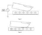
- FIG. 1is a simple diagram of an electric field biometric scanner mechanism showing the source of charge and the distributed capacitance layer that is the sensor's outer platen surface.
- FIG. 2is a simplified schematic diagram showing an electric field biometric scanner measurement circuit that receives the electric charge to measure.
- the fingeris simply shown as a node in the circuit between the detector and the electric field source.
- FIG. 3is a simplified schematic diagram showing an electric field biometric scanner measurement circuit that receives the electric charge to measure.
- the fingeris shown bridging multiple pixel nodes in the detection circuit; finger resistance shorts between adjacent capacitors.
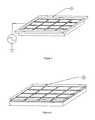
- FIG. 4depicts an array of electric field sensors (TFT or CMOS).
- FIG. 5shows an electric field sensor array configured as an electric field type fingerprint scanner.
- FIG. 6shows an electric field sensor array configured as a capacitance type fingerprint scanner.
- FIG. 7is an exploded view of the scanner depicted in FIG. 5 .
- FIG. 8is an exploded view of the scanner depicted in FIG. 6 .
- FIG. 9is a diagram of the operation of the electric field type fingerprint scanner.
- FIG. 10is a diagram of the operation of the capacitance type fingerprint scanner.
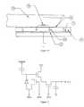
- FIG. 11depicts a TFT electric field detection pixel schematic.
- FIG. 12depicts a schematic of the pixel capacitance skin resistance network at any multiple friction skin contact points.
- FIG. 13is a flow chart depicting a method according to the invention.
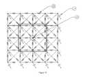
- FIG. 14is a system according to the invention.
- the inventionmay be embodied as a method of operating an electric field biometric scanner.
- FIGS. 1-5 , 7 and 9depict an electric field finger scanner, when operated according to the prior art.
- Such a scannermeasures the local electric field coming from the surface of a biometric object, such as skin that is in contact with a dielectric layer serving as an imaging platen.
- the scannerincludes (a) an electric field excitation generator, (b) an array of electrodes, (c) a dielectric layer covering the electrode array, and (d) electric field sensors electrically connected to the electrode array.
- FIGS. 1 through 9show aspects of an electric field scanner. For the purpose of clarity, most of the discussion will reference FIG. 9 .
- a voltage source 7that radiates via an antenna (or bus) 6 that is in contact with the finger 9 .
- the electric fieldconducts through the finger resistance 10 and emerges through the friction skin surface that is in contact with the dielectric surface 4 of a fingerprint reader 1 , where the dielectric surface 4 is disposed uniformly over an array of electrodes 3 , each connected to an electric field detecting and measuring circuit in an array of such circuits 2 of a TFT.
- the individual circuitsmay be row and column addressed and read to provide information to a computer system that displays the area read and the electrical field variation that is associated with each pixel circuit.
- the circuit for an individual pixel on a TFTis shown in the schematic diagram that is FIG. 11 .
- the electric field coming from the fingerprint ridgesis stronger than that coming from the fingerprint valleys, and the measured values can by collectively displayed as an image that is a true representation of the fingerprint.
- the userplaces a finger 9 in contact with the dielectric platen surface 4 , while also contacting the electric field generator's (i.e., transmitter's) antenna (or excitation bus) 6 that may take the form of a metal ring that is the perimeter of the fingerprint platen area.
- the finger 9receives and radiates the electric field through the dielectric to the pixel electrode plates 3 that are attached to the electric field detecting circuits 2 .
- the electric fieldvaries in intensity in direct correlation with the finger's fingerprint valleys and ridges.
- the sensor outputsare read out in row and column fashion to allow the reading electronic system to reconstruct a grayscale fingerprint image analogous to the variations in the electric field radiating from the finger's ridge and valley skin surface.
- the electric field scanneris operated without the electric field generator. This may be accomplished by turning off the generator, or grounding the output of the generator so that no electric field is provided to the finger. In this mode, the scanner may be operated as a capacitance fingerprint scanner.
- the signal emanating from each electric field sensoris primarily representative of two things:
- the reading from a particular electric field sensor and the readings from adjacent electric field sensorsare processed to obtain a value which is then attributed to the location of that particular electric field sensor. This process is repeated for each electric field sensor to provide and attribute a value to each electric field sensor location.
- FIG. 13depicts such a method in flow-chart form.
- a deviceuses electric field sensors capacitively coupled to a finger that is not being excited by an electric field generator.
- the fieldis conducted through the skin of the finger and coupled through the dielectric platen to the input electrode of the electric field detecting circuit.
- the individual pixel circuits, each sensor being part of a pixel, on the TFTare read out via row and column addressing, and the signals are interpreted and translated into an image representation of the TFT array in order to allow for the creation of an image of the fingerprint associated with the finger that is in contact with the dielectric platen.
- FIG. 10shows an electric field finger scanner without the electric field generator.
- the electric field deviceis operated without the electric field generating device 7 or antenna 6 .
- the sensoroperates as a capacitance fingerprint scanner device 8 and when the finger contacts the dielectric platen 4 , the finger completes a resistance-capacitance circuit between adjacent pixel input plates using the resistance 10 of the finger 9 . Since this shared charge capacitance receives contributions from multiple pixel input plates 3 , the charge is distributed between sensors pixels 2 where the center pixel shares charge with each of its neighbors.
- This capacitive charge sharingis sufficient to maintain line sharpness and image quality across the sensor surface with the center-contacting-skin pixel receiving a share many times more (approximately 8 for most sensors) than that of any of its immediate neighbors, such as in FIG. 12 .
- the actual distributed circuitextends outward in all directions and there are contributions from all of the pixels, it is considered for explanation purposes, that only the 8 (for most sensors) immediate neighboring pixels, share a connection with any pixel-of-interest 13 , since the contribution from pixels outside of this region are negligible.
- FIG. 14depicts a system according to the invention.
- the electric field devicewith no electric field generator
- a computeris programmed to process the capacitance readings of the electric field sensors in the manner outlined above.
- Such a computermay be programmed to sum the capacitance reading of a particular electric field sensor with the readings from adjacent electric field sensors, and then divide by the number of sensors contributing to that sum. The resulting value is then attributed to that particular sensor location. This process may be carried out by the computer for all electric field sensors in order to provide a value corresponding to each sensor location.
- the values generated by the computermay then be used by the computer to generate an image of the fingerprint, or the values may be used to make a comparison with information in a database in order to determine whether the fingerprint matches a previously analyzed fingerprint.
Landscapes
- Engineering & Computer Science (AREA)
- Theoretical Computer Science (AREA)
- Physics & Mathematics (AREA)
- General Physics & Mathematics (AREA)
- Human Computer Interaction (AREA)
- General Engineering & Computer Science (AREA)
- Multimedia (AREA)
- Computer Vision & Pattern Recognition (AREA)
- Image Input (AREA)
- Measurement Of Length, Angles, Or The Like Using Electric Or Magnetic Means (AREA)
- Measurement Of The Respiration, Hearing Ability, Form, And Blood Characteristics Of Living Organisms (AREA)
- Chemical & Material Sciences (AREA)
- Chemical Kinetics & Catalysis (AREA)
- Electrochemistry (AREA)
- Health & Medical Sciences (AREA)
- Life Sciences & Earth Sciences (AREA)
- Analytical Chemistry (AREA)
- Biochemistry (AREA)
- General Health & Medical Sciences (AREA)
- Immunology (AREA)
- Pathology (AREA)
Abstract
Description
- This application claims the benefit of priority to U.S. provisional patent application Ser. No. 61/595,322, filed on Feb. 6, 2012.
- The invention relates to fingerprint scanning devices that function by means of measuring the electric field associated with the distributed charge on a biometric object, such as a finger.
- Since the 1800's fingerprint information has been collected from human fingers and hands by means of ink and paper. For the purposes of this document, the term fingerprint is used to mean the skin surface friction ridge detail of a single fingerprint, partial fingerprint or any portion of the skin surface friction ridge up to and including the entire hand or foot. In recent years various electronic fingerprint scanning systems have been developed utilizing optical, capacitance, direct pressure, thermal, and acoustic methods. Methods based upon acoustics, ultrasound, capacitance, and electric field measurement have proven to be the most accurate, as they are virtually immune to the effects of grease, dirt, paint, ink, and other image contaminants. Capacitance sensors may also offer additional advantage in that they may be able to achieve improved imaging in cases where poor acoustic impedance matching between the friction skin of the fingerprint and the scanner's platen are present, such as may be encountered when the skin on the finger is very dry.
- The electric field method employs a transducer that capacitively couples the finger to an array of electric field measuring devices. The electric field may be a static field or one that employs a generating device that is coupled to the finger by contact with an electrode. Although the electric field is nearly uniform across the finger, there are variations in the electric field that give rise to differences in the measured electric field. For example, when a ridge of the friction skin of the finger is present, the measured electric field will be different than when a valley of the friction skin is present. Graphically displaying this information creates a contour map of the object (human finger or skin surface) that is in contact with the scanner surface. For example, the depth of any gap structure, such as the ridges and valleys of the fingerprint, may be displayed as a gray-scale bitmap image. Measuring the electric field via the capacitance coupling to the platen surface makes use of the fact that the electric field is a function of the distance between capacitance plates, i.e., the TFT input pad and the skin of the finger. Ridges of the fingerprint are closer to the input pad and valleys are places where the skin is farther away from the TFT input electrode pad, and thus differing electric field measurements that can be used to identify the location of the ridges and valleys of the fingerprint.
- The invention may be embodied as a biometric scanner having an electric field device and a computer coupled to a sensor array. The electric field device (a) has no electric field generator or an electric field generator that is prevented from providing an electric field to a biometric object, such as a finger, and (b) has an electric field sensor array comprised of a plurality of electric field sensors. The computer is communicatively coupled to the sensor array in order to receive capacitance readings from the sensors. The computer is programmed to process the capacitance readings as follows:
- (i) identify a particular one of the electric field sensors that is providing a capacitance reading;
- (ii) sum the capacitance reading of the identified electric field sensor with capacitance readings from adjacent electric field sensors;
- (iii) divide the sum by the number of sensors contributing to that sum to provide a value;
- (iv) attribute the value to the identified sensor;
- (v) repeat steps (i) through (iv) until a value has been attributed to all sensors.
- The computer may be further programmed to create an image of the biometric object using the values attributed to each sensor. The computer may be further programmed to use the values in determining whether the biometric object matches information in a database.
- The invention may be embodied as a method of scanning a biometric object. Such a method may:
- (i) provide100 an electric field device (a) having no electric field generator or an electric field generator that is prevented from providing an electric field to a biometric object, and (b) having an electric field sensor array comprised of a plurality of electric field sensors;
- (ii) provide103 a biometric object in contact with the electric field device;
- (iii) identify106 a particular one of the electric field sensors that is providing a capacitance reading;
- (iv) sum109 the capacitance reading of the identified electric field sensor with capacitance readings from adjacent electric field sensors;
- (v) divide the sum by the number of sensors contributing to that sum to provide a value;
- (vi)
attribute 112 the value to the identified sensor; - (vii) repeat115 steps (iii) through (vi) until a value has been attributed to all sensors; and
- (viii) provide118 the values as being representative of the biometric object.
- The method may further comprise accepting the provided values and using the values to generate a visual image of the biometric object. The method may further comprise accepting the provided values and using the values to determine whether the biometric object matches information in a database.
- For a fuller understanding of the nature and objects of the invention, reference should be made to the accompanying drawings and the subsequent description. Briefly, the drawings are:
FIG. 1 is a simple diagram of an electric field biometric scanner mechanism showing the source of charge and the distributed capacitance layer that is the sensor's outer platen surface.FIG. 2 is a simplified schematic diagram showing an electric field biometric scanner measurement circuit that receives the electric charge to measure. The finger is simply shown as a node in the circuit between the detector and the electric field source.FIG. 3 is a simplified schematic diagram showing an electric field biometric scanner measurement circuit that receives the electric charge to measure. The finger is shown bridging multiple pixel nodes in the detection circuit; finger resistance shorts between adjacent capacitors.FIG. 4 depicts an array of electric field sensors (TFT or CMOS).FIG. 5 shows an electric field sensor array configured as an electric field type fingerprint scanner.FIG. 6 shows an electric field sensor array configured as a capacitance type fingerprint scanner.FIG. 7 is an exploded view of the scanner depicted inFIG. 5 .FIG. 8 is an exploded view of the scanner depicted inFIG. 6 .FIG. 9 is a diagram of the operation of the electric field type fingerprint scanner.FIG. 10 is a diagram of the operation of the capacitance type fingerprint scanner.FIG. 11 depicts a TFT electric field detection pixel schematic.FIG. 12 depicts a schematic of the pixel capacitance skin resistance network at any multiple friction skin contact points.FIG. 13 is a flow chart depicting a method according to the invention.FIG. 14 is a system according to the invention.- In the figures, certain reference numbers appear. These reference numbers indicate:
- 1 electric field scanner
- 2 TFT circuits
- 3 electrode array
- 4 dielectric layer
- 5 TFT substrate
- 6 antenna or excitation bus
- 7 excitation source (electric field generator)
- 8 capacitance scanner
- 9 finger
- 10 resistance path through the finger
- 11 capacitance plate (part of body conductive finger surface)
- 12 capacitance through the
dielectric layer 4 from theelectrode 3 to thefinger 9 - 13 schematic of finger friction skin resistance and sensor capacitances for a plurality of contact nodes on the platen with the node of interest indicated
- 14 sensor capacitance between any sensor element of the
electrode array 3 and thefinger 9 - 15 skin resistance
- The invention may be embodied as a method of operating an electric field biometric scanner.
FIGS. 1-5 ,7 and9 depict an electric field finger scanner, when operated according to the prior art. Such a scanner measures the local electric field coming from the surface of a biometric object, such as skin that is in contact with a dielectric layer serving as an imaging platen. The scanner includes (a) an electric field excitation generator, (b) an array of electrodes, (c) a dielectric layer covering the electrode array, and (d) electric field sensors electrically connected to the electrode array. FIGS. 1 through 9 show aspects of an electric field scanner. For the purpose of clarity, most of the discussion will referenceFIG. 9 . InFIG. 9 , there is shown avoltage source 7 that radiates via an antenna (or bus)6 that is in contact with thefinger 9. The electric field conducts through thefinger resistance 10 and emerges through the friction skin surface that is in contact with thedielectric surface 4 of a fingerprint reader1, where thedielectric surface 4 is disposed uniformly over an array ofelectrodes 3, each connected to an electric field detecting and measuring circuit in an array ofsuch circuits 2 of a TFT. The individual circuits may be row and column addressed and read to provide information to a computer system that displays the area read and the electrical field variation that is associated with each pixel circuit. The circuit for an individual pixel on a TFT is shown in the schematic diagram that isFIG. 11 . As is known in the prior art, the electric field coming from the fingerprint ridges is stronger than that coming from the fingerprint valleys, and the measured values can by collectively displayed as an image that is a true representation of the fingerprint.- To operate the fingerprint scanner according to the prior art, the user places a
finger 9 in contact with thedielectric platen surface 4, while also contacting the electric field generator's (i.e., transmitter's) antenna (or excitation bus)6 that may take the form of a metal ring that is the perimeter of the fingerprint platen area. Thefinger 9 receives and radiates the electric field through the dielectric to thepixel electrode plates 3 that are attached to the electricfield detecting circuits 2. The electric field varies in intensity in direct correlation with the finger's fingerprint valleys and ridges. After detecting and measuring this electric field variation at eachelectric field sensor 2, the sensor outputs are read out in row and column fashion to allow the reading electronic system to reconstruct a grayscale fingerprint image analogous to the variations in the electric field radiating from the finger's ridge and valley skin surface. - In a method according to the invention, the electric field scanner is operated without the electric field generator. This may be accomplished by turning off the generator, or grounding the output of the generator so that no electric field is provided to the finger. In this mode, the scanner may be operated as a capacitance fingerprint scanner. The signal emanating from each electric field sensor is primarily representative of two things:
- (a) the capacitance between an electrode, the dielectric material covering the electrode and the skin that covers the dielectric material, and
- (b) the capacitance between the electrode, the dielectric material covering adjacent electrodes, and the skin that covers the dielectric material covering those adjacent portions of the dielectric material.
Ideally, the signal emanating from each electric field sensor would not be influenced by the capacitance described in item “b”, and instead would be only that capacitance that is attributable to item “a”. - In order to compensate for that part of the capacitance corresponding to item “b”, the reading from a particular electric field sensor and the readings from adjacent electric field sensors are processed to obtain a value which is then attributed to the location of that particular electric field sensor. This process is repeated for each electric field sensor to provide and attribute a value to each electric field sensor location. These attributed values corresponding to the capacitances are used as the information representing the fingerprint.
- A particular process that works well is to sum the reading of a particular electric field sensor with the readings from adjacent electric field sensors, and then divide by the number of sensors contributing to that sum. So, if a particular sensor has eight adjacent sensors, the divisor will be nine. However, if a particular sensor has five adjacent sensors, then the divisor will be six.
FIG. 13 depicts such a method in flow-chart form. - In use, a device according to the invention uses electric field sensors capacitively coupled to a finger that is not being excited by an electric field generator. As the finger contacts a dielectric platen covering the array of electric field detecting and measuring circuits on a TFT array, the field is conducted through the skin of the finger and coupled through the dielectric platen to the input electrode of the electric field detecting circuit. The individual pixel circuits, each sensor being part of a pixel, on the TFT are read out via row and column addressing, and the signals are interpreted and translated into an image representation of the TFT array in order to allow for the creation of an image of the fingerprint associated with the finger that is in contact with the dielectric platen.
- Having provided an overview of a method according to the invention, a device according to the invention will be described, and in doing so additional details about the inventive method will be provided.
FIG. 10 shows an electric field finger scanner without the electric field generator. The electric field device is operated without the electricfield generating device 7 orantenna 6. In this case, the sensor operates as a capacitancefingerprint scanner device 8 and when the finger contacts thedielectric platen 4, the finger completes a resistance-capacitance circuit between adjacent pixel input plates using theresistance 10 of thefinger 9. Since this shared charge capacitance receives contributions from multiplepixel input plates 3, the charge is distributed betweensensors pixels 2 where the center pixel shares charge with each of its neighbors. This capacitive charge sharing is sufficient to maintain line sharpness and image quality across the sensor surface with the center-contacting-skin pixel receiving a share many times more (approximately 8 for most sensors) than that of any of its immediate neighbors, such as inFIG. 12 . Although the actual distributed circuit extends outward in all directions and there are contributions from all of the pixels, it is considered for explanation purposes, that only the 8 (for most sensors) immediate neighboring pixels, share a connection with any pixel-of-interest 13, since the contribution from pixels outside of this region are negligible. FIG. 14 depicts a system according to the invention. InFIG. 14 there is shown the electric field device (with no electric field generator) and a computer. The computer is programmed to process the capacitance readings of the electric field sensors in the manner outlined above. Such a computer may be programmed to sum the capacitance reading of a particular electric field sensor with the readings from adjacent electric field sensors, and then divide by the number of sensors contributing to that sum. The resulting value is then attributed to that particular sensor location. This process may be carried out by the computer for all electric field sensors in order to provide a value corresponding to each sensor location. The values generated by the computer may then be used by the computer to generate an image of the fingerprint, or the values may be used to make a comparison with information in a database in order to determine whether the fingerprint matches a previously analyzed fingerprint.- Although the present invention has been described with respect to one or more particular embodiments, it will be understood that other embodiments of the present invention may be made without departing from the spirit and scope of the present invention. Hence, the present invention is deemed limited only by the appended claims and the reasonable interpretation thereof.
Claims (6)
Priority Applications (2)
| Application Number | Priority Date | Filing Date | Title |
|---|---|---|---|
| US13/760,954US9619689B2 (en) | 2012-02-06 | 2013-02-06 | System and method of using an electric field device |
| US15/173,416US9740911B2 (en) | 2012-02-06 | 2016-06-03 | System and method of using an electric field device |
Applications Claiming Priority (2)
| Application Number | Priority Date | Filing Date | Title |
|---|---|---|---|
| US201261595322P | 2012-02-06 | 2012-02-06 | |
| US13/760,954US9619689B2 (en) | 2012-02-06 | 2013-02-06 | System and method of using an electric field device |
Related Child Applications (1)
| Application Number | Title | Priority Date | Filing Date |
|---|---|---|---|
| US15/173,416ContinuationUS9740911B2 (en) | 2012-02-06 | 2016-06-03 | System and method of using an electric field device |
Publications (2)
| Publication Number | Publication Date |
|---|---|
| US20130200907A1true US20130200907A1 (en) | 2013-08-08 |
| US9619689B2 US9619689B2 (en) | 2017-04-11 |
Family
ID=48902352
Family Applications (2)
| Application Number | Title | Priority Date | Filing Date |
|---|---|---|---|
| US13/760,954Expired - Fee RelatedUS9619689B2 (en) | 2012-02-06 | 2013-02-06 | System and method of using an electric field device |
| US15/173,416Expired - Fee RelatedUS9740911B2 (en) | 2012-02-06 | 2016-06-03 | System and method of using an electric field device |
Family Applications After (1)
| Application Number | Title | Priority Date | Filing Date |
|---|---|---|---|
| US15/173,416Expired - Fee RelatedUS9740911B2 (en) | 2012-02-06 | 2016-06-03 | System and method of using an electric field device |
Country Status (8)
| Country | Link |
|---|---|
| US (2) | US9619689B2 (en) |
| EP (1) | EP2812851A4 (en) |
| JP (1) | JP6133904B2 (en) |
| KR (1) | KR20140119099A (en) |
| CN (1) | CN104380312B (en) |
| IN (1) | IN2014MN01393A (en) |
| TW (1) | TW201351302A (en) |
| WO (1) | WO2013119697A1 (en) |
Cited By (14)
| Publication number | Priority date | Publication date | Assignee | Title |
|---|---|---|---|---|
| US20130314105A1 (en)* | 2012-05-04 | 2013-11-28 | Apple Inc. | Electronic device including device ground coupled finger coupling electrode and array shielding electrode and related methods |
| US20140159746A1 (en)* | 2012-11-02 | 2014-06-12 | Palo Alto Research Center Incorporated | Capacitive imaging device with active pixels |
| US9215392B2 (en) | 2014-04-21 | 2015-12-15 | Palo Alto Research Center Incorporated | Impedance readout circuit and method having filter for determining an AC current component inversely proportional to the output impedance of a pixel |
| US20160064166A1 (en)* | 2014-08-27 | 2016-03-03 | Continental Automotive Systems, Inc. | Switch with user feedback |
| CN106372567A (en)* | 2015-07-23 | 2017-02-01 | 瑞鼎科技股份有限公司 | Capacitive fingerprint sensing device and capacitive fingerprint sensing method |
| US9582705B2 (en) | 2014-08-31 | 2017-02-28 | Qualcomm Incorporated | Layered filtering for biometric sensors |
| US20170132883A1 (en)* | 2015-10-09 | 2017-05-11 | Soberlink Healthcare, Llc | Bioresistive-fingerprint based sobriety monitoring system |
| US9665763B2 (en)* | 2014-08-31 | 2017-05-30 | Qualcomm Incorporated | Finger/non-finger determination for biometric sensors |
| US9740911B2 (en) | 2012-02-06 | 2017-08-22 | Qualcomm Incorporated | System and method of using an electric field device |
| US9911184B2 (en) | 2014-08-31 | 2018-03-06 | Qualcomm Incorporated | Air/object determination for biometric sensors |
| US10101373B2 (en) | 2014-04-21 | 2018-10-16 | Palo Alto Research Center Incorporated | Capacitive imaging device with active pixels and method |
| WO2019004905A1 (en)* | 2017-06-28 | 2019-01-03 | Fingerprint Cards Ab | Fingerprint sensor module comprising antenna and method for manufacturing a fingerprint sensor module |
| US10203816B2 (en) | 2013-05-07 | 2019-02-12 | Egis Technology Inc. | Apparatus and method for TFT fingerprint sensor |
| US20190065142A1 (en)* | 2017-08-31 | 2019-02-28 | Samsung Electronics Co., Ltd. | Electronic apparatus, input device and method for control thereof |
Citations (19)
| Publication number | Priority date | Publication date | Assignee | Title |
|---|---|---|---|---|
| US4811414A (en)* | 1987-02-27 | 1989-03-07 | C.F.A. Technologies, Inc. | Methods for digitally noise averaging and illumination equalizing fingerprint images |
| US6411727B1 (en)* | 1998-02-05 | 2002-06-25 | Koninklijke Philips Electronics N.V. | Fingerprint sensing devices and systems incorporating such |
| US6518820B2 (en)* | 2000-02-05 | 2003-02-11 | E.G.O. Elektro-Geraetebau Gmbh | Circuit arrangement having a capacitive sensor element for a touch contact switch |
| US6714666B1 (en)* | 1999-06-10 | 2004-03-30 | Nippon Telegraph And Telephone Corporation | Surface shape recognition apparatus |
| US20050094855A1 (en)* | 2003-10-29 | 2005-05-05 | Proano Cesar H. | Fingerprint imaging using a flat panel detector |
| US20070024546A1 (en)* | 2005-07-27 | 2007-02-01 | Jin Jang | Unevenness detecting apparatus for compensating for threshold voltage and method thereof |
| US20080208495A1 (en)* | 2007-02-22 | 2008-08-28 | Teradyne, Inc. | Electrically stimulated fingerprint sensor test method |
| US20090016571A1 (en)* | 2007-03-30 | 2009-01-15 | Louis Tijerina | Blur display for automotive night vision systems with enhanced form perception from low-resolution camera images |
| US20090079707A1 (en)* | 2007-09-24 | 2009-03-26 | Motorola, Inc. | Integrated capacitive sensing devices and methods |
| US20090256815A1 (en)* | 2008-04-14 | 2009-10-15 | Microsoft Corporation | Active matrix touch sensing |
| US20100276604A1 (en)* | 2007-08-23 | 2010-11-04 | Fujifilm Corporation | Image detecting device |
| US20110215150A1 (en)* | 2010-03-08 | 2011-09-08 | Schneider John K | Biometric Sensor With Delay Layer |
| US20110221684A1 (en)* | 2010-03-11 | 2011-09-15 | Sony Ericsson Mobile Communications Ab | Touch-sensitive input device, mobile device and method for operating a touch-sensitive input device |
| US20110242044A1 (en)* | 2010-04-06 | 2011-10-06 | Au Optronics Corporation | In-cell touch sensing panel |
| US20120050220A1 (en)* | 2010-08-24 | 2012-03-01 | Au Optronics Corporation | Touch Panel |
| US20120144920A1 (en)* | 2010-12-10 | 2012-06-14 | Palo Alto Research Center Incorporated | Ultrasonic imaging using thin film transistor backplane |
| US20130106758A1 (en)* | 2011-10-26 | 2013-05-02 | Nokia Corporation | Apparatus and Associated Methods |
| US8441459B2 (en)* | 2008-09-30 | 2013-05-14 | Hannstar Display Corporation | In-cell capacitive touch panel |
| US8618865B1 (en)* | 2012-11-02 | 2013-12-31 | Palo Alto Research Center Incorporated | Capacitive imaging device with active pixels |
Family Cites Families (13)
| Publication number | Priority date | Publication date | Assignee | Title |
|---|---|---|---|---|
| US4728931A (en)* | 1986-07-25 | 1988-03-01 | Honeywell Inc. | Charge redistribution capacitance detection apparatus |
| US5963679A (en)* | 1996-01-26 | 1999-10-05 | Harris Corporation | Electric field fingerprint sensor apparatus and related methods |
| US6483931B2 (en)* | 1997-09-11 | 2002-11-19 | Stmicroelectronics, Inc. | Electrostatic discharge protection of a capacitve type fingerprint sensing array |
| JP2002092603A (en)* | 2000-09-14 | 2002-03-29 | Ntt Electornics Corp | Device and method for detecting fingerprint |
| US6672174B2 (en)* | 2001-07-23 | 2004-01-06 | Fidelica Microsystems, Inc. | Fingerprint image capture device with a passive sensor array |
| KR100564915B1 (en)* | 2004-02-10 | 2006-03-30 | 한국과학기술원 | Capacitive fingerprint sensor and fingerprint sensing method using same |
| JP4441927B2 (en)* | 2004-10-12 | 2010-03-31 | セイコーエプソン株式会社 | Capacitance detection device |
| TWM268676U (en) | 2004-12-28 | 2005-06-21 | Lite On Semiconductor Corp | Fingerprint scan device and electric equipment with fingerprint scan function |
| US7923240B2 (en)* | 2006-03-31 | 2011-04-12 | Intel Corporation | Photo-activated field effect transistor for bioanalyte detection |
| US20080122454A1 (en)* | 2006-11-29 | 2008-05-29 | Aisin Seiki Kabushiki Kaisha | Capacitance detecting apparatus |
| US7773228B1 (en) | 2007-08-15 | 2010-08-10 | Itn Energy Systems, Inc. | Surface plasmon noncontact electric field sensors and related methods |
| KR101323045B1 (en)* | 2008-10-21 | 2013-10-29 | 엘지디스플레이 주식회사 | Sensing deving and method for amplifying output thereof |
| CN104380312B (en) | 2012-02-06 | 2018-07-10 | 高通股份有限公司 | Use the system and method for electric field arrangement |
- 2013
- 2013-02-06CNCN201380007918.2Apatent/CN104380312B/ennot_activeExpired - Fee Related
- 2013-02-06EPEP13746756.9Apatent/EP2812851A4/ennot_activeWithdrawn
- 2013-02-06JPJP2014555856Apatent/JP6133904B2/ennot_activeExpired - Fee Related
- 2013-02-06KRKR1020147021938Apatent/KR20140119099A/ennot_activeCeased
- 2013-02-06TWTW102104705Apatent/TW201351302A/enunknown
- 2013-02-06ININ1393MUN2014patent/IN2014MN01393A/enunknown
- 2013-02-06USUS13/760,954patent/US9619689B2/ennot_activeExpired - Fee Related
- 2013-02-06WOPCT/US2013/024973patent/WO2013119697A1/enactiveApplication Filing
- 2016
- 2016-06-03USUS15/173,416patent/US9740911B2/ennot_activeExpired - Fee Related
Patent Citations (19)
| Publication number | Priority date | Publication date | Assignee | Title |
|---|---|---|---|---|
| US4811414A (en)* | 1987-02-27 | 1989-03-07 | C.F.A. Technologies, Inc. | Methods for digitally noise averaging and illumination equalizing fingerprint images |
| US6411727B1 (en)* | 1998-02-05 | 2002-06-25 | Koninklijke Philips Electronics N.V. | Fingerprint sensing devices and systems incorporating such |
| US6714666B1 (en)* | 1999-06-10 | 2004-03-30 | Nippon Telegraph And Telephone Corporation | Surface shape recognition apparatus |
| US6518820B2 (en)* | 2000-02-05 | 2003-02-11 | E.G.O. Elektro-Geraetebau Gmbh | Circuit arrangement having a capacitive sensor element for a touch contact switch |
| US20050094855A1 (en)* | 2003-10-29 | 2005-05-05 | Proano Cesar H. | Fingerprint imaging using a flat panel detector |
| US20070024546A1 (en)* | 2005-07-27 | 2007-02-01 | Jin Jang | Unevenness detecting apparatus for compensating for threshold voltage and method thereof |
| US20080208495A1 (en)* | 2007-02-22 | 2008-08-28 | Teradyne, Inc. | Electrically stimulated fingerprint sensor test method |
| US20090016571A1 (en)* | 2007-03-30 | 2009-01-15 | Louis Tijerina | Blur display for automotive night vision systems with enhanced form perception from low-resolution camera images |
| US20100276604A1 (en)* | 2007-08-23 | 2010-11-04 | Fujifilm Corporation | Image detecting device |
| US20090079707A1 (en)* | 2007-09-24 | 2009-03-26 | Motorola, Inc. | Integrated capacitive sensing devices and methods |
| US20090256815A1 (en)* | 2008-04-14 | 2009-10-15 | Microsoft Corporation | Active matrix touch sensing |
| US8441459B2 (en)* | 2008-09-30 | 2013-05-14 | Hannstar Display Corporation | In-cell capacitive touch panel |
| US20110215150A1 (en)* | 2010-03-08 | 2011-09-08 | Schneider John K | Biometric Sensor With Delay Layer |
| US20110221684A1 (en)* | 2010-03-11 | 2011-09-15 | Sony Ericsson Mobile Communications Ab | Touch-sensitive input device, mobile device and method for operating a touch-sensitive input device |
| US20110242044A1 (en)* | 2010-04-06 | 2011-10-06 | Au Optronics Corporation | In-cell touch sensing panel |
| US20120050220A1 (en)* | 2010-08-24 | 2012-03-01 | Au Optronics Corporation | Touch Panel |
| US20120144920A1 (en)* | 2010-12-10 | 2012-06-14 | Palo Alto Research Center Incorporated | Ultrasonic imaging using thin film transistor backplane |
| US20130106758A1 (en)* | 2011-10-26 | 2013-05-02 | Nokia Corporation | Apparatus and Associated Methods |
| US8618865B1 (en)* | 2012-11-02 | 2013-12-31 | Palo Alto Research Center Incorporated | Capacitive imaging device with active pixels |
Cited By (20)
| Publication number | Priority date | Publication date | Assignee | Title |
|---|---|---|---|---|
| US9740911B2 (en) | 2012-02-06 | 2017-08-22 | Qualcomm Incorporated | System and method of using an electric field device |
| US9581628B2 (en)* | 2012-05-04 | 2017-02-28 | Apple Inc. | Electronic device including device ground coupled finger coupling electrode and array shielding electrode and related methods |
| US20130314105A1 (en)* | 2012-05-04 | 2013-11-28 | Apple Inc. | Electronic device including device ground coupled finger coupling electrode and array shielding electrode and related methods |
| US20140159746A1 (en)* | 2012-11-02 | 2014-06-12 | Palo Alto Research Center Incorporated | Capacitive imaging device with active pixels |
| EP2728512A3 (en)* | 2012-11-02 | 2015-07-01 | Palo Alto Research Center Incorporated | Capacitive imaging device with active pixels |
| US9964575B2 (en)* | 2012-11-02 | 2018-05-08 | Palo Alto Research Center Incorporated | Capacitive imaging device with active pixels |
| US10203816B2 (en) | 2013-05-07 | 2019-02-12 | Egis Technology Inc. | Apparatus and method for TFT fingerprint sensor |
| US10101373B2 (en) | 2014-04-21 | 2018-10-16 | Palo Alto Research Center Incorporated | Capacitive imaging device with active pixels and method |
| US9215392B2 (en) | 2014-04-21 | 2015-12-15 | Palo Alto Research Center Incorporated | Impedance readout circuit and method having filter for determining an AC current component inversely proportional to the output impedance of a pixel |
| US9838009B2 (en)* | 2014-08-27 | 2017-12-05 | Continental Automotive Systems, Inc. | Switch with user feedback |
| US20160064166A1 (en)* | 2014-08-27 | 2016-03-03 | Continental Automotive Systems, Inc. | Switch with user feedback |
| US9665763B2 (en)* | 2014-08-31 | 2017-05-30 | Qualcomm Incorporated | Finger/non-finger determination for biometric sensors |
| US9582705B2 (en) | 2014-08-31 | 2017-02-28 | Qualcomm Incorporated | Layered filtering for biometric sensors |
| US9911184B2 (en) | 2014-08-31 | 2018-03-06 | Qualcomm Incorporated | Air/object determination for biometric sensors |
| CN106372567A (en)* | 2015-07-23 | 2017-02-01 | 瑞鼎科技股份有限公司 | Capacitive fingerprint sensing device and capacitive fingerprint sensing method |
| US20170132883A1 (en)* | 2015-10-09 | 2017-05-11 | Soberlink Healthcare, Llc | Bioresistive-fingerprint based sobriety monitoring system |
| US9922508B2 (en)* | 2015-10-09 | 2018-03-20 | Soberlink Healthcare, Llc | Bioresistive-fingerprint based sobriety monitoring system |
| WO2019004905A1 (en)* | 2017-06-28 | 2019-01-03 | Fingerprint Cards Ab | Fingerprint sensor module comprising antenna and method for manufacturing a fingerprint sensor module |
| US20190065142A1 (en)* | 2017-08-31 | 2019-02-28 | Samsung Electronics Co., Ltd. | Electronic apparatus, input device and method for control thereof |
| US10789043B2 (en)* | 2017-08-31 | 2020-09-29 | Samsung Electronics Co., Ltd. | Electronic apparatus, input device and method for control thereof |
Also Published As
| Publication number | Publication date |
|---|---|
| CN104380312A (en) | 2015-02-25 |
| IN2014MN01393A (en) | 2015-04-03 |
| WO2013119697A1 (en) | 2013-08-15 |
| KR20140119099A (en) | 2014-10-08 |
| TW201351302A (en) | 2013-12-16 |
| EP2812851A1 (en) | 2014-12-17 |
| US20160283767A1 (en) | 2016-09-29 |
| US9740911B2 (en) | 2017-08-22 |
| US9619689B2 (en) | 2017-04-11 |
| JP6133904B2 (en) | 2017-05-24 |
| EP2812851A4 (en) | 2016-06-08 |
| CN104380312B (en) | 2018-07-10 |
| JP2015508922A (en) | 2015-03-23 |
Similar Documents
| Publication | Publication Date | Title |
|---|---|---|
| US9740911B2 (en) | System and method of using an electric field device | |
| JP6190689B2 (en) | Capacitive image forming apparatus having active pixels | |
| TWI441087B (en) | Finger sensing device with differential measuring circuit and related method | |
| USRE45650E1 (en) | Apparatus and method for reducing parasitic capacitive coupling and noise in fingerprint sensing circuits | |
| CN102246061B (en) | Positioning device | |
| US9576176B2 (en) | Noise compensation in a biometric sensing device | |
| CN110070006A (en) | Fingerprint identification method, electronic device and computer-readable medium | |
| CN107924260A (en) | Multiphase fingerprint sensor is laid out and structure | |
| CN107710225A (en) | Fingerprint acquisition apparatus and method therein for noise measuring | |
| CN108694373A (en) | The adaptive reference that differential capacitive measures | |
| US10102412B2 (en) | Fingerprint sensing with different capacitive configurations | |
| US20050094855A1 (en) | Fingerprint imaging using a flat panel detector | |
| US9699396B2 (en) | Surface contact imaging sensor | |
| US20130214801A1 (en) | Pressure-based Fingerprint Authentication Device | |
| CN108701222B (en) | Fingerprint sensing using measurement structures having different main directions of extension | |
| CN108229409B (en) | Ultrasonic fingerprint detection assembly and method and display device | |
| US20150300799A1 (en) | Capacitive imaging device with active pixels and method | |
| US9922231B1 (en) | Fingerprint sensing with voltage pattern configurations | |
| RU2001109244A (en) | METHOD AND DEVICE FOR CAPACITIVE DEFINITION OF THE IMAGE | |
| US11935319B2 (en) | Method and system for fingerprint sensor evaluation | |
| Eom et al. | A Multi-Purpose Fingerprint Readout Circuit Embedding Physiological Signal Detection | |
| TW201800920A (en) | Capacitive detecting device and driving method |
Legal Events
| Date | Code | Title | Description |
|---|---|---|---|
| AS | Assignment | Owner name:QUALCOMM INCORPORATED, CALIFORNIA Free format text:ASSIGNMENT OF ASSIGNORS INTEREST;ASSIGNOR:ULTRA-SCAN CORPORATION;REEL/FRAME:030416/0069 Effective date:20130507 | |
| AS | Assignment | Owner name:ULTRA-SCAN CORPORATION, NEW YORK Free format text:NUNC PRO TUNC ASSIGNMENT;ASSIGNORS:SCHNEIDER, JOHN K;KITCHENS, JACK C;REEL/FRAME:038232/0967 Effective date:20120206 | |
| AS | Assignment | Owner name:ULTRA-SCAN CORPORATION, NEW YORK Free format text:ASSIGNMENT OF ASSIGNORS INTEREST;ASSIGNORS:SCHNEIDER, JOHN K;KITCHENS, JACK C;REEL/FRAME:038963/0456 Effective date:20120206 | |
| FEPP | Fee payment procedure | Free format text:PAYOR NUMBER ASSIGNED (ORIGINAL EVENT CODE: ASPN); ENTITY STATUS OF PATENT OWNER: LARGE ENTITY | |
| STCF | Information on status: patent grant | Free format text:PATENTED CASE | |
| FEPP | Fee payment procedure | Free format text:MAINTENANCE FEE REMINDER MAILED (ORIGINAL EVENT CODE: REM.); ENTITY STATUS OF PATENT OWNER: LARGE ENTITY | |
| LAPS | Lapse for failure to pay maintenance fees | Free format text:PATENT EXPIRED FOR FAILURE TO PAY MAINTENANCE FEES (ORIGINAL EVENT CODE: EXP.); ENTITY STATUS OF PATENT OWNER: LARGE ENTITY | |
| STCH | Information on status: patent discontinuation | Free format text:PATENT EXPIRED DUE TO NONPAYMENT OF MAINTENANCE FEES UNDER 37 CFR 1.362 | |
| FP | Lapsed due to failure to pay maintenance fee | Effective date:20210411 |