US20130187261A1 - Semiconductor device - Google Patents
Semiconductor deviceDownload PDFInfo
- Publication number
- US20130187261A1 US20130187261A1US13/745,330US201313745330AUS2013187261A1US 20130187261 A1US20130187261 A1US 20130187261A1US 201313745330 AUS201313745330 AUS 201313745330AUS 2013187261 A1US2013187261 A1US 2013187261A1
- Authority
- US
- United States
- Prior art keywords
- semiconductor chip
- mount region
- mount
- fixedly attached
- semiconductor device
- Prior art date
- Legal status (The legal status is an assumption and is not a legal conclusion. Google has not performed a legal analysis and makes no representation as to the accuracy of the status listed.)
- Granted
Links
- 239000004065semiconductorSubstances0.000titleclaimsabstractdescription180
- 239000000463materialSubstances0.000claimsabstractdescription44
- 230000001070adhesive effectEffects0.000claimsabstractdescription40
- 239000000853adhesiveSubstances0.000claimsabstractdescription39
- 239000011347resinSubstances0.000claimsdescription21
- 229920005989resinPolymers0.000claimsdescription21
- 239000004642PolyimideSubstances0.000claimsdescription5
- 229920001721polyimidePolymers0.000claimsdescription5
- 229920001296polysiloxanePolymers0.000claimsdescription3
- 238000007789sealingMethods0.000claimsdescription3
- 238000001514detection methodMethods0.000abstractdescription4
- 239000003990capacitorSubstances0.000description7
- 230000000630rising effectEffects0.000description6
- 238000002955isolationMethods0.000description4
- RYGMFSIKBFXOCR-UHFFFAOYSA-NCopperChemical compound[Cu]RYGMFSIKBFXOCR-UHFFFAOYSA-N0.000description3
- 229910052802copperInorganic materials0.000description3
- 239000010949copperSubstances0.000description3
- 238000005530etchingMethods0.000description3
- 238000000034methodMethods0.000description3
- 238000005516engineering processMethods0.000description2
- 238000004519manufacturing processMethods0.000description2
- 238000000059patterningMethods0.000description2
- 229910000679solderInorganic materials0.000description2
- 230000012447hatchingEffects0.000description1
- 239000011810insulating materialSubstances0.000description1
- 229910052759nickelInorganic materials0.000description1
- 229910052763palladiumInorganic materials0.000description1
- 230000035945sensitivityEffects0.000description1
- 229910052709silverInorganic materials0.000description1
- 238000005476solderingMethods0.000description1
Images


Classifications
- H—ELECTRICITY
- H01—ELECTRIC ELEMENTS
- H01L—SEMICONDUCTOR DEVICES NOT COVERED BY CLASS H10
- H01L21/00—Processes or apparatus adapted for the manufacture or treatment of semiconductor or solid state devices or of parts thereof
- H01L21/02—Manufacture or treatment of semiconductor devices or of parts thereof
- H01L21/04—Manufacture or treatment of semiconductor devices or of parts thereof the devices having potential barriers, e.g. a PN junction, depletion layer or carrier concentration layer
- H01L21/50—Assembly of semiconductor devices using processes or apparatus not provided for in a single one of the groups H01L21/18 - H01L21/326 or H10D48/04 - H10D48/07 e.g. sealing of a cap to a base of a container
- H01L21/56—Encapsulations, e.g. encapsulation layers, coatings
- H—ELECTRICITY
- H01—ELECTRIC ELEMENTS
- H01L—SEMICONDUCTOR DEVICES NOT COVERED BY CLASS H10
- H01L23/00—Details of semiconductor or other solid state devices
- H01L23/34—Arrangements for cooling, heating, ventilating or temperature compensation ; Temperature sensing arrangements
- H—ELECTRICITY
- H01—ELECTRIC ELEMENTS
- H01L—SEMICONDUCTOR DEVICES NOT COVERED BY CLASS H10
- H01L23/00—Details of semiconductor or other solid state devices
- H01L23/48—Arrangements for conducting electric current to or from the solid state body in operation, e.g. leads, terminal arrangements ; Selection of materials therefor
- H01L23/488—Arrangements for conducting electric current to or from the solid state body in operation, e.g. leads, terminal arrangements ; Selection of materials therefor consisting of soldered or bonded constructions
- H01L23/495—Lead-frames or other flat leads
- H01L23/49503—Lead-frames or other flat leads characterised by the die pad
- H01L23/49513—Lead-frames or other flat leads characterised by the die pad having bonding material between chip and die pad
- H—ELECTRICITY
- H01—ELECTRIC ELEMENTS
- H01L—SEMICONDUCTOR DEVICES NOT COVERED BY CLASS H10
- H01L23/00—Details of semiconductor or other solid state devices
- H01L23/48—Arrangements for conducting electric current to or from the solid state body in operation, e.g. leads, terminal arrangements ; Selection of materials therefor
- H01L23/488—Arrangements for conducting electric current to or from the solid state body in operation, e.g. leads, terminal arrangements ; Selection of materials therefor consisting of soldered or bonded constructions
- H01L23/495—Lead-frames or other flat leads
- H01L23/49575—Assemblies of semiconductor devices on lead frames
- H—ELECTRICITY
- H01—ELECTRIC ELEMENTS
- H01L—SEMICONDUCTOR DEVICES NOT COVERED BY CLASS H10
- H01L23/00—Details of semiconductor or other solid state devices
- H01L23/48—Arrangements for conducting electric current to or from the solid state body in operation, e.g. leads, terminal arrangements ; Selection of materials therefor
- H01L23/488—Arrangements for conducting electric current to or from the solid state body in operation, e.g. leads, terminal arrangements ; Selection of materials therefor consisting of soldered or bonded constructions
- H01L23/498—Leads, i.e. metallisations or lead-frames on insulating substrates, e.g. chip carriers
- H—ELECTRICITY
- H01—ELECTRIC ELEMENTS
- H01L—SEMICONDUCTOR DEVICES NOT COVERED BY CLASS H10
- H01L2224/00—Indexing scheme for arrangements for connecting or disconnecting semiconductor or solid-state bodies and methods related thereto as covered by H01L24/00
- H01L2224/01—Means for bonding being attached to, or being formed on, the surface to be connected, e.g. chip-to-package, die-attach, "first-level" interconnects; Manufacturing methods related thereto
- H01L2224/26—Layer connectors, e.g. plate connectors, solder or adhesive layers; Manufacturing methods related thereto
- H01L2224/31—Structure, shape, material or disposition of the layer connectors after the connecting process
- H01L2224/32—Structure, shape, material or disposition of the layer connectors after the connecting process of an individual layer connector
- H01L2224/321—Disposition
- H01L2224/32151—Disposition the layer connector connecting between a semiconductor or solid-state body and an item not being a semiconductor or solid-state body, e.g. chip-to-substrate, chip-to-passive
- H01L2224/32221—Disposition the layer connector connecting between a semiconductor or solid-state body and an item not being a semiconductor or solid-state body, e.g. chip-to-substrate, chip-to-passive the body and the item being stacked
- H01L2224/32245—Disposition the layer connector connecting between a semiconductor or solid-state body and an item not being a semiconductor or solid-state body, e.g. chip-to-substrate, chip-to-passive the body and the item being stacked the item being metallic
- H—ELECTRICITY
- H01—ELECTRIC ELEMENTS
- H01L—SEMICONDUCTOR DEVICES NOT COVERED BY CLASS H10
- H01L2224/00—Indexing scheme for arrangements for connecting or disconnecting semiconductor or solid-state bodies and methods related thereto as covered by H01L24/00
- H01L2224/01—Means for bonding being attached to, or being formed on, the surface to be connected, e.g. chip-to-package, die-attach, "first-level" interconnects; Manufacturing methods related thereto
- H01L2224/42—Wire connectors; Manufacturing methods related thereto
- H01L2224/47—Structure, shape, material or disposition of the wire connectors after the connecting process
- H01L2224/48—Structure, shape, material or disposition of the wire connectors after the connecting process of an individual wire connector
- H01L2224/481—Disposition
- H01L2224/48135—Connecting between different semiconductor or solid-state bodies, i.e. chip-to-chip
- H01L2224/48137—Connecting between different semiconductor or solid-state bodies, i.e. chip-to-chip the bodies being arranged next to each other, e.g. on a common substrate
- H—ELECTRICITY
- H01—ELECTRIC ELEMENTS
- H01L—SEMICONDUCTOR DEVICES NOT COVERED BY CLASS H10
- H01L2224/00—Indexing scheme for arrangements for connecting or disconnecting semiconductor or solid-state bodies and methods related thereto as covered by H01L24/00
- H01L2224/01—Means for bonding being attached to, or being formed on, the surface to be connected, e.g. chip-to-package, die-attach, "first-level" interconnects; Manufacturing methods related thereto
- H01L2224/42—Wire connectors; Manufacturing methods related thereto
- H01L2224/47—Structure, shape, material or disposition of the wire connectors after the connecting process
- H01L2224/48—Structure, shape, material or disposition of the wire connectors after the connecting process of an individual wire connector
- H01L2224/481—Disposition
- H01L2224/48151—Connecting between a semiconductor or solid-state body and an item not being a semiconductor or solid-state body, e.g. chip-to-substrate, chip-to-passive
- H01L2224/48221—Connecting between a semiconductor or solid-state body and an item not being a semiconductor or solid-state body, e.g. chip-to-substrate, chip-to-passive the body and the item being stacked
- H01L2224/48245—Connecting between a semiconductor or solid-state body and an item not being a semiconductor or solid-state body, e.g. chip-to-substrate, chip-to-passive the body and the item being stacked the item being metallic
- H01L2224/48247—Connecting between a semiconductor or solid-state body and an item not being a semiconductor or solid-state body, e.g. chip-to-substrate, chip-to-passive the body and the item being stacked the item being metallic connecting the wire to a bond pad of the item
- H—ELECTRICITY
- H01—ELECTRIC ELEMENTS
- H01L—SEMICONDUCTOR DEVICES NOT COVERED BY CLASS H10
- H01L2224/00—Indexing scheme for arrangements for connecting or disconnecting semiconductor or solid-state bodies and methods related thereto as covered by H01L24/00
- H01L2224/01—Means for bonding being attached to, or being formed on, the surface to be connected, e.g. chip-to-package, die-attach, "first-level" interconnects; Manufacturing methods related thereto
- H01L2224/42—Wire connectors; Manufacturing methods related thereto
- H01L2224/47—Structure, shape, material or disposition of the wire connectors after the connecting process
- H01L2224/49—Structure, shape, material or disposition of the wire connectors after the connecting process of a plurality of wire connectors
- H01L2224/491—Disposition
- H01L2224/4912—Layout
- H01L2224/49171—Fan-out arrangements
- H—ELECTRICITY
- H01—ELECTRIC ELEMENTS
- H01L—SEMICONDUCTOR DEVICES NOT COVERED BY CLASS H10
- H01L2224/00—Indexing scheme for arrangements for connecting or disconnecting semiconductor or solid-state bodies and methods related thereto as covered by H01L24/00
- H01L2224/73—Means for bonding being of different types provided for in two or more of groups H01L2224/10, H01L2224/18, H01L2224/26, H01L2224/34, H01L2224/42, H01L2224/50, H01L2224/63, H01L2224/71
- H01L2224/732—Location after the connecting process
- H01L2224/73251—Location after the connecting process on different surfaces
- H01L2224/73265—Layer and wire connectors
- H—ELECTRICITY
- H01—ELECTRIC ELEMENTS
- H01L—SEMICONDUCTOR DEVICES NOT COVERED BY CLASS H10
- H01L2924/00—Indexing scheme for arrangements or methods for connecting or disconnecting semiconductor or solid-state bodies as covered by H01L24/00
- H01L2924/10—Details of semiconductor or other solid state devices to be connected
- H01L2924/11—Device type
- H01L2924/13—Discrete devices, e.g. 3 terminal devices
- H01L2924/1304—Transistor
- H01L2924/1305—Bipolar Junction Transistor [BJT]
- H01L2924/13055—Insulated gate bipolar transistor [IGBT]
- H—ELECTRICITY
- H01—ELECTRIC ELEMENTS
- H01L—SEMICONDUCTOR DEVICES NOT COVERED BY CLASS H10
- H01L2924/00—Indexing scheme for arrangements or methods for connecting or disconnecting semiconductor or solid-state bodies as covered by H01L24/00
- H01L2924/15—Details of package parts other than the semiconductor or other solid state devices to be connected
- H01L2924/181—Encapsulation
- H—ELECTRICITY
- H01—ELECTRIC ELEMENTS
- H01L—SEMICONDUCTOR DEVICES NOT COVERED BY CLASS H10
- H01L2924/00—Indexing scheme for arrangements or methods for connecting or disconnecting semiconductor or solid-state bodies as covered by H01L24/00
- H01L2924/19—Details of hybrid assemblies other than the semiconductor or other solid state devices to be connected
- H01L2924/191—Disposition
- H01L2924/19101—Disposition of discrete passive components
- H01L2924/19105—Disposition of discrete passive components in a side-by-side arrangement on a common die mounting substrate
Definitions
- the present inventionrelates to a semiconductor device in which a driving semiconductor chip and a controlling semiconductor chip for controlling the driving semiconductor chip are incorporated in a semiconductor package for use, for example, in an on-board igniter.
- the following structurehas been known as an example of conventional semiconductor devices.
- a semiconductor element 63 and chip capacitors 64are fixedly attached to the top of a stage 62 formed of a lead frame in a semiconductor device 61 .
- the stage 62is formed larger than the semiconductor element 63 .
- the chip capacitors 64are mounted outside the semiconductor element 63 on the stage 62 .
- a recessed portion 65is formed by half-etching the stage 62 from its top surface.
- an insulating tape 66such as a polyimide tape is placed inside the recessed portion 65 .
- the chip capacitor 64is fixedly attached to the top of the insulating tape 66 .
- This structureprevents the chip capacitors 64 from being short-circuited to the corresponding semiconductor element 63 via the stage 62 .
- This technologyis described, for instance, in Japanese Patent Application Publication No. 2006-245618 (pp. 4 to 5, and FIGS. 5 to 8).
- an IC (integrated circuit) chip 72is fixedly attached to the principal surface of a tab 71 of the two divided tabs, while electronic parts 74 are fixedly attached to the principal surface of the other tab 73 .
- the structure in which the tabs 71 , 73 are at least divided from each otherprevents the electronic parts 74 from being short-circuited to the IC chip 72 via the tabs 71 , 73 .
- an insulating film 75may be formed on the principal surface of the other tab 73 . This technology is described, for instance, in Japanese Utility Model Registration Application Publication No. Sho 63-187353 (pp. 4 to 5, and FIGS. 1 to 2) in a microfilm form.
- a resin package of the on-board igniterincludes, for example, a driving semiconductor chip as a switching element and a controlling semiconductor chip for controlling the driving semiconductor chip.
- the driving semiconductor chipincludes an embedded larger-current element such as an IGBT (insulated gate bipolar transistor).
- the controlling semiconductor chipincludes a temperature detecting element and a thermal shutdown circuit, and is placed near the driving semiconductor chip.
- the controlling semiconductor chipdetects the temperature of the driving semiconductor chip. When detecting a temperature higher than a preset value, the controlling semiconductor chip forcibly makes the driving semiconductor chip perform an OFF operation, and thereby prevents the temperature of the driving semiconductor chip from rising abnormally and prevents the driving semiconductor chip from catching fire.
- the driving semiconductor chip and the controlling semiconductor chipare placed on the same island as shown in FIG. 7 , the temperature rising state of the driving semiconductor chip can be accurately detected.
- the use of the insulating tapeprevents the short circuit between the two semiconductor chips, the structure in which the two semiconductor chips are placed on the same island poses a problem that the two semiconductor chips are more likely to be short-circuited to each other due to processing errors in the manufacturing, such as errors in position recognition during the insulating tape applying step and the die bonding step.
- the potential of the islandis equal to the potential applied to the driving semiconductor chip. For this reason, if a different potential is intended to be applied to the controlling semiconductor chip, the lead needs to be patterned up to the vicinity of the island. This patterning poses another problem of limiting the freedom in pattern design.
- the structure in which the tabs are divided from each other as shown in FIG. 8poses yet another problem that conditions for processing the lead frame make it difficult to reduce the distance between the driving semiconductor chip and the controlling semiconductor chip beyond some extent.
- the controlling semiconductor chipdetects the temperature rising state of the driving semiconductor chip through the resin forming the resin package in most cases, this structure poses still another problem that a relationship in thermal conductivity between the materials makes it difficult to accurately detect the rise in the temperature of the driving semiconductor chip.
- a semiconductor device of the present inventionis a semiconductor device including: a first mount region; a second mount region placed near the first mount region, and formed isolated from the first mount region; leads placed near the first and second mount regions; a first semiconductor chip fixedly attached to a top of the first mount region; a second semiconductor chip fixedly attached to tops of the respective first and second mount regions, and configured to control the first semiconductor chip; a resin sealing body covering the first and second mount regions, the leads, and the first and second semiconductor chips, in which a projecting area protruding into the second mount region is formed in the first mount region, and the second semiconductor chip is fixedly attached to the tops of the first and second mount regions by use of an insulating adhesive sheet material in a way that at least part of the projecting area is placed under the second semiconductor chip.
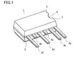
- FIG. 1is a perspective view for explaining a semiconductor device of a first embodiment of the present invention.
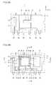
- FIGS. 2A and 2Bare plan views for explaining the semiconductor device of the first embodiment of the present invention.
- FIGS. 3A and 3Bare cross-sectional views for explaining the semiconductor device of the first embodiment of the present invention.
- FIGS. 4A and 4Bare plan views for explaining a semiconductor device of a second embodiment of the present invention.
- FIGS. 5A and 5Bare cross-sectional views for explaining the semiconductor device of the second embodiment of the present invention.
- FIGS. 6A and 6Bare plan views for explaining the semiconductor device of another embodiment of the present invention.
- FIG. 7is a perspective view for explaining a semiconductor device of a conventional embodiment.
- FIG. 8is a perspective view for explaining a semiconductor device of another conventional embodiment.
- FIG. 1is a perspective view of the semiconductor device taken from the top surface of the semiconductor device.
- FIG. 2Ais a plan views for explaining a frame structure used for the semiconductor device shown in FIG. 1 .
- FIG. 2Bis a plan view for explaining an inner structure of the semiconductor device shown in FIG. 1 .
- FIG. 3Ais a cross-sectional view for explaining the semiconductor device taken along the A-A line of FIG. 2B .
- FIG. 3Bis a cross-sectional view for explaining the semiconductor device taken along the B-B line of FIG. 2B .
- a resin package 2 of a semiconductor device 1is shaped like a rectangular parallelepiped. Multiple leads 4 a to 4 f are drawn out from a longitudinal side surface 3 of the resin package 2 .
- a U-shaped hole 6 as a screw stopperis placed in a side surface 5 of the resin package 2 which extends in a short length direction thereof. Note that, albeit unillustrated, the leads 4 are bent in a right-angled shape, and fixed to the mount board inside a through-hole by soldering.
- FIG. 2Ashows a frame 7 which is placed inside the resin package 2 .
- a frame made from a material essentially containing copperis used as the frame 7 .
- a frame made from a material essentially containing Femay be used as the frame 7 .
- the thickness of the frame 7is 200 ⁇ m, for example.
- first to fourth mount regions 8 , 9 , 10 , 11 and the multiple leads 4 a to 4 fare defined by performing etching, blanking, and other processes on the frame 7 .
- a chain line 12indicates the external form line of the resin package 2 .
- the first mount region 8is formed integrated with the lead 4 a in a Y-axis direction in the drawing.
- the first mount region 8includes a projecting area 8 a formed in a shape protruding into the second mount region 9 in an X-axis direction in the drawing.
- the projecting area 8 ais isolated from the second mount region 9 by an isolation groove 13 .
- the projecting area 8 ahas a structure which extends up to under a semiconductor chip 15 (see FIG. 2B ) fixedly attached to the second mount region 9 . It is desirable that the projecting area 8 a should protrude by at least a half of the width (i.e., the width in the X-axis direction) of the second mount region 9 .
- the second mount region 9includes a recessed area 9 a formed in a shape recessed to surround the projecting area 8 a in the X-axis direction in the drawing. Furthermore, because the semiconductor chip 15 fixedly attached to the second mount region 9 is placed over the recessed area 9 a , the width (i.e., the width in the Y-axis direction) of the recessed area 9 a is narrower than the width of the semiconductor chip 15 . To serve this purpose, the recessed area 9 a only needs to surround at least part of the projecting area 8 a with the width of the isolation groove 13 adjusted.
- the multiple leads 4 a to 4 fare placed to be drawn out from the side surface 3 of the resin package 2 . Moreover, the leads 4 b to 4 d are placed near the first and second mount regions 8 , 9 .
- the lead 4 eis formed integrated with the third mount region 10
- the lead 4 fis formed integrated with the fourth mount region 11 .
- the frame 7is plated with Pd, Ag, Ni/Pd/Ag, or the like.
- FIG. 2Bshows the frame to which the semiconductor chips and the like are fixedly attached.
- a switching elementa driving element
- a discrete semiconductor chip 14 having a built-in IGBTfor example, is fixedly attached to the first mount region 8 by use of an adhesive 20 such as Ag paste, solder or the like (see FIG. 3A ).
- the semiconductor chip 15 having a built-in LSI element for controlling the semiconductor chip 14is fixedly attached to the second mount region 9 by use of an insulating adhesive sheet material 16 .
- a thermal shutdown circuitis formed by placing, for example, a thermal detection element on the top surface of the semiconductor chip 15 .
- the semiconductor chip 15detects the temperature rising state of the semiconductor chip 14 , and forcibly shuts down the semiconductor chip 14 if the temperature of the semiconductor chip 14 rises beyond a set temperature.
- the adhesive sheet material 16may be placed to additionally cover the above of the isolation groove 13 and extends onto the first mount region 8 .
- the flatness between the first mount region 8 and the second mount region 9is easily maintained by the adhesive sheet material 16 , and the second semiconductor chip 15 is fixedly attached thereto stably as well.
- yields in the wire bonding processincrease because the failure in connecting thin metallic wires occurs less often.
- a semiconductor chip 17is fixedly attached to the third mount region 10 by use of a conductive adhesive, and a chip capacitor 18 is fixedly attached to the third and fourth mount regions 10 , 11 by use of an adhesive 21 (see FIG. 3A ), such as Ag paste or solder.
- an adhesive 21such as Ag paste or solder.
- the semiconductor chips 14 , 15 and the likeare electrically connected together by use of thin metallic wires 19 .
- the resin package 2 for an on-board igniterfor example, which includes the thermal shutdown circuit, is formed.
- FIG. 3Ashows the cross section of the resin package 2 taken along the A-A line (see FIG. 2B ).
- the semiconductor chip 14is fixedly attached to the top of the first mount region 8 by the adhesive 20
- the semiconductor chip 15is fixedly attached to the top of the projecting area 8 a of the first mount region 8 and the top of the second mount region 9 by use of the adhesive sheet material 16 .
- the adhesive sheet material 16is formed from an insulating material having an adhesive property, such as a polyimide tape, a silicone tape or a DAF (Die Attach Film) material.
- the polyimide tapeAs the adhesive sheet material 16 , the thickness of the adhesive sheet material 16 can be made thinner and the temperature detection sensitivity of the adhesive sheet material 16 can be increased.
- the chip capacitor 18is fixedly attached to the third and fourth mount regions 10 , 11 by use of the adhesive 21 .
- heat produced by the semiconductor chip 14transmits to the first mount region 8 , and further transmits to the lower portion of the semiconductor chip 15 via the projecting area 8 a .
- the frame 7is formed from the material essentially containing copper, the frame 7 is better in thermal conductivity than the resin material from which the resin package 2 is made. This structure enables the semiconductor chip 15 to detect the temperature rising state of the semiconductor chip 14 through the frame 7 as well. Accordingly, the temperature condition of the semiconductor chip 14 can be detected more accurately. If the temperature of the semiconductor chip 14 rises abnormally, the semiconductor chip 14 is shut down immediately so as not to catch fire.
- the area of the frame 7 which is better in thermal conductivityis increased by making the projecting area 8 a protrude by at least a half of the width (i.e., the width in the X-axis direction) of the semiconductor chip 15 . Accordingly, the semiconductor chip 15 is capable of detecting the temperature condition of the semiconductor chip 14 more accurately.
- the semiconductor chip 15is prevented from being short-circuited to the semiconductor chip 14 through the projecting area 8 a.
- FIG. 3Bshows the cross section of the resin package 2 taken along the B-B line (see FIG. 2B ).
- the semiconductor chip 15is fixedly attached to the top of the projecting area 8 a of the first mount region 8 and the top of the second mount region 9 by use of the adhesive sheet material 16 . Furthermore, because as indicated with circles 22 , the adhesive sheet material 16 is placed up to the outside of the end portions of the semiconductor chip 15 , the problem of the above-mentioned short circuit does not occur.
- the fixed attachment of the semiconductor chip 15is achieved by placing the semiconductor chip 15 on the adhesive sheet material 16 after placing the adhesive sheet material 16 on the top surfaces of the first and second mount regions 8 , 9 . Even if the end portion of the semiconductor chip 15 comes closer to or in contact with the second mount region 9 due to errors in position recognition and the like during the manufacturing process, the problem of the above-mentioned short circuit does not occur since the first and second mount regions 8 , 9 are isolated by the isolation groove 13 .
- the descriptionshave been provided particularly for the case where no potential is applied to the second mount region 9 .
- the embodimentis not limited to this case.
- an embodimentmay be carried out by using the second mount region 9 as the ground potential of the semiconductor chip 15 .
- the design freedom of the frame patterningis enhanced because the number of leads placed near the second mount region 9 is reduced.
- FIG. 4Ais a plan view for explaining a frame structure used for the semiconductor device shown in FIG. 1 .
- FIG. 4Bis a plan view for explaining an internal structure of the semiconductor device shown in FIG. 1 .
- FIG. 5Ais a cross-sectional view for explaining the internal structure thereof taken along the C-C line of FIG. 4B .
- FIG. 5Bis a cross-sectional view for explaining the internal structure thereof taken along the D-D line of FIG. 4B .
- components which are the same as those of the first embodimentwill be denoted by the same reference numerals. The descriptions of such components are referred to by the reference numerals, and are omitted here.
- FIG. 4Ashows a frame 31 placed inside a resin package 2 , which is indicated with a chain line 32 .
- a frame made from a material essentially containing copperis used as the frame 31 in common with the frame 7 .
- a frame made from a material essentially containing Femay be used as the frame 31 .
- first to third mount regions 33 to 35 and multiple leads 4 a to 4 fare defined by performing etching, blanking, and other processes on the frame 31 .
- the first mount region 33is formed in a shape which represents the integral combination of the first and second mount regions 8 , 9 of the first embodiment; the second mount region 34 corresponds to the third mount region 10 of the first embodiment; and the third mount region 35 corresponds to the fourth mount region 11 of the first embodiment.
- the first mount region 33is formed integral with the lead 4 a in a Y-axis direction in the drawings.
- an opening 36is formed in a left portion of the first mount region 33 in an X-axis direction in the drawings.
- This opening 36has an opening shape which is larger than a semiconductor chip 15 .
- FIG. 4Bshows the frame to which the semiconductor chips and the like are fixedly attached.
- a semiconductor chip 14is fixedly attached to the top surface of the first mount region 33 by use of an adhesive 20 .
- an adhesive sheet material 37is adhered to the back surface of the first mount region 33 in a way that closes the opening 36 .
- the semiconductor chip 15is fixedly attached to the top surface of the adhesive sheet material 37 inside the opening 36 , and the end portion of the semiconductor chip 15 is placed away from the first mount region 33 .
- the adhesive material 37is formed from the same material as is the adhesive sheet material 16 of the first embodiment.
- the semiconductor chip 15is capable of detecting the temperature rising state of the semiconductor chip 14 with much higher accuracy, since the distance by which the semiconductor chips 14 , 15 are away from each other can be shortened compared with the structure in which the semiconductor chips 14 , are fixedly attached to the respective discrete mount regions.
- the foregoing descriptionshave been provided for the case where: the one driving semiconductor chip 14 is placed in the resin package 2 ; and the semiconductor chip 14 is controlled by the one controlling semiconductor chip.
- the embodimentsare not limited to this case.
- an embodimentmay be carried out by: placing four driving semiconductor chips 40 in a resin package indicated with a chain line 39 ; and controlling the four driving semiconductor chips 40 by use of one controlling semiconductor chip 41 .
- the four semiconductor chips 40are fixedly attached to the top surfaces of the respective discrete mount regions 42 to 45 , while the semiconductor chip 41 is fixedly attached to the top of an adhesive sheet material 46 .
- the flatness among the mount regions 42 to 45is also maintained by the adhesive sheet material 46 in the above-described manner.
- an embodimentmay be carried out by: placing 6 driving semiconductor chips 48 in a resin package indicated with a chain line 47 ; and controlling the 6 driving semiconductor chips 48 by use of one controlling semiconductor chip 49 .
- the 6 semiconductor chips 48are fixedly attached to the top surfaces of the respective discrete mount regions 50 to 55
- the semiconductor chip 49is fixedly attached to the top of an adhesive sheet material 56 .
- the flatness among the mount regions 50 to 55is also maintained by the adhesive sheet material 56 in the above-described manner.
- the driving semiconductor chip and the controlling semiconductor chipare fixedly attached to the tops of the respective discrete mount regions, and the part of the mount region to which the driving semiconductor chip is fixedly attached is placed up to under the controlling semiconductor chip.
- This structureenables the controlling semiconductor chip to detect the temperature of the driving semiconductor chip via the mount region.
- most of the end portion of the controlling semiconductor chipis placed on the second mount region. This realizes the structure which makes the driving semiconductor chip and the controlling semiconductor chip less likely to be short-circuited to each other.
- the controlling semiconductor chipdetects the temperature of the driving semiconductor chip accurately, and shuts down the driving semiconductor chip appropriately. This makes the driving semiconductor chip less likely to be broken down due to the heat.
- the mount region to which the driving semiconductor chip is fixedly attached and the mount region to which the controlling semiconductor chip is fixedly attachedare placed isolated from each other. This makes it possible to apply different potentials to the respective mount regions.
- the controlling semiconductor chipis fixedly attached to the top of the corresponding mount region by use of the insulating adhesive sheet material. This prevents the short circuit between the two semiconductor chips while maintaining the temperature detecting function of the controlling semiconductor chip.
- the openingis formed in the mount region to which the driving semiconductor chip is fixedly attached, and the controlling semiconductor chip is fixedly attached by use of the insulating adhesive sheet material through the opening. This prevents the short circuit between the two semiconductor chips.
Landscapes
- Engineering & Computer Science (AREA)
- Physics & Mathematics (AREA)
- Condensed Matter Physics & Semiconductors (AREA)
- General Physics & Mathematics (AREA)
- Computer Hardware Design (AREA)
- Microelectronics & Electronic Packaging (AREA)
- Power Engineering (AREA)
- Manufacturing & Machinery (AREA)
- Cooling Or The Like Of Semiconductors Or Solid State Devices (AREA)
- Lead Frames For Integrated Circuits (AREA)
- Die Bonding (AREA)
- Structures Or Materials For Encapsulating Or Coating Semiconductor Devices Or Solid State Devices (AREA)
Abstract
Description
- This application claims priority from Japanese Patent Application No. 2012-008952 filed on Jan. 19, 2012, the contents of which are incorporated herein by reference in its entirety.
- 1. Field of the Invention
- The present invention relates to a semiconductor device in which a driving semiconductor chip and a controlling semiconductor chip for controlling the driving semiconductor chip are incorporated in a semiconductor package for use, for example, in an on-board igniter.
- 2. Description of the Related Art
- The following structure has been known as an example of conventional semiconductor devices.
- As shown in
FIG. 7 , asemiconductor element 63 andchip capacitors 64 are fixedly attached to the top of astage 62 formed of a lead frame in asemiconductor device 61. Thestage 62 is formed larger than thesemiconductor element 63. Thechip capacitors 64 are mounted outside thesemiconductor element 63 on thestage 62. In each of the mount regions of thechip capacitors 64, arecessed portion 65 is formed by half-etching thestage 62 from its top surface. As illustrated, aninsulating tape 66 such as a polyimide tape is placed inside therecessed portion 65. Thechip capacitor 64 is fixedly attached to the top of theinsulating tape 66. This structure prevents thechip capacitors 64 from being short-circuited to thecorresponding semiconductor element 63 via thestage 62. This technology is described, for instance, in Japanese Patent Application Publication No. 2006-245618 (pp. 4 to 5, and FIGS. 5 to 8). - In addition, the following structure has been known as another example of the conventional semiconductor devices.
- As shown in
FIG. 8 , an IC (integrated circuit)chip 72 is fixedly attached to the principal surface of atab 71 of the two divided tabs, whileelectronic parts 74 are fixedly attached to the principal surface of theother tab 73. The structure in which thetabs electronic parts 74 from being short-circuited to theIC chip 72 via thetabs insulating film 75 may be formed on the principal surface of theother tab 73. This technology is described, for instance, in Japanese Utility Model Registration Application Publication No. Sho 63-187353 (pp. 4 to 5, and FIGS. 1 to 2) in a microfilm form. - A resin package of the on-board igniter includes, for example, a driving semiconductor chip as a switching element and a controlling semiconductor chip for controlling the driving semiconductor chip. The driving semiconductor chip includes an embedded larger-current element such as an IGBT (insulated gate bipolar transistor). The controlling semiconductor chip includes a temperature detecting element and a thermal shutdown circuit, and is placed near the driving semiconductor chip. The controlling semiconductor chip detects the temperature of the driving semiconductor chip. When detecting a temperature higher than a preset value, the controlling semiconductor chip forcibly makes the driving semiconductor chip perform an OFF operation, and thereby prevents the temperature of the driving semiconductor chip from rising abnormally and prevents the driving semiconductor chip from catching fire.
- In this case, if the driving semiconductor chip and the controlling semiconductor chip are placed on the same island as shown in
FIG. 7 , the temperature rising state of the driving semiconductor chip can be accurately detected. Although the use of the insulating tape prevents the short circuit between the two semiconductor chips, the structure in which the two semiconductor chips are placed on the same island poses a problem that the two semiconductor chips are more likely to be short-circuited to each other due to processing errors in the manufacturing, such as errors in position recognition during the insulating tape applying step and the die bonding step. - Furthermore, in the structure in which the two semiconductor chips are placed on the same island, the potential of the island is equal to the potential applied to the driving semiconductor chip. For this reason, if a different potential is intended to be applied to the controlling semiconductor chip, the lead needs to be patterned up to the vicinity of the island. This patterning poses another problem of limiting the freedom in pattern design.
- On the other hand, the structure in which the tabs are divided from each other as shown in
FIG. 8 poses yet another problem that conditions for processing the lead frame make it difficult to reduce the distance between the driving semiconductor chip and the controlling semiconductor chip beyond some extent. In addition, since the controlling semiconductor chip detects the temperature rising state of the driving semiconductor chip through the resin forming the resin package in most cases, this structure poses still another problem that a relationship in thermal conductivity between the materials makes it difficult to accurately detect the rise in the temperature of the driving semiconductor chip. - The present invention has been made in view of the above-described circumstances. A semiconductor device of the present invention is a semiconductor device including: a first mount region; a second mount region placed near the first mount region, and formed isolated from the first mount region; leads placed near the first and second mount regions; a first semiconductor chip fixedly attached to a top of the first mount region; a second semiconductor chip fixedly attached to tops of the respective first and second mount regions, and configured to control the first semiconductor chip; a resin sealing body covering the first and second mount regions, the leads, and the first and second semiconductor chips, in which a projecting area protruding into the second mount region is formed in the first mount region, and the second semiconductor chip is fixedly attached to the tops of the first and second mount regions by use of an insulating adhesive sheet material in a way that at least part of the projecting area is placed under the second semiconductor chip.
FIG. 1 is a perspective view for explaining a semiconductor device of a first embodiment of the present invention.FIGS. 2A and 2B are plan views for explaining the semiconductor device of the first embodiment of the present invention.FIGS. 3A and 3B are cross-sectional views for explaining the semiconductor device of the first embodiment of the present invention.FIGS. 4A and 4B are plan views for explaining a semiconductor device of a second embodiment of the present invention.FIGS. 5A and 5B are cross-sectional views for explaining the semiconductor device of the second embodiment of the present invention.FIGS. 6A and 6B are plan views for explaining the semiconductor device of another embodiment of the present invention.FIG. 7 is a perspective view for explaining a semiconductor device of a conventional embodiment.FIG. 8 is a perspective view for explaining a semiconductor device of another conventional embodiment.- Descriptions will be hereinbelow provided for a semiconductor device of a first embodiment of the present invention.
FIG. 1 is a perspective view of the semiconductor device taken from the top surface of the semiconductor device.FIG. 2A is a plan views for explaining a frame structure used for the semiconductor device shown inFIG. 1 .FIG. 2B is a plan view for explaining an inner structure of the semiconductor device shown inFIG. 1 .FIG. 3A is a cross-sectional view for explaining the semiconductor device taken along the A-A line ofFIG. 2B .FIG. 3B is a cross-sectional view for explaining the semiconductor device taken along the B-B line ofFIG. 2B . - As shown in
FIG. 1 , aresin package 2 of asemiconductor device 1 is shaped like a rectangular parallelepiped. Multiple leads4ato4fare drawn out from alongitudinal side surface 3 of theresin package 2. On the other hand, aU-shaped hole 6 as a screw stopper is placed in aside surface 5 of theresin package 2 which extends in a short length direction thereof. Note that, albeit unillustrated, the leads4 are bent in a right-angled shape, and fixed to the mount board inside a through-hole by soldering. FIG. 2A shows aframe 7 which is placed inside theresin package 2. Generally, a frame made from a material essentially containing copper is used as theframe 7. Otherwise, a frame made from a material essentially containing Fe may be used as theframe 7. In addition, the thickness of theframe 7 is 200 μm, for example. Furthermore, first tofourth mount regions multiple leads 4ato4f, for example, are defined by performing etching, blanking, and other processes on theframe 7. Note that achain line 12 indicates the external form line of theresin package 2.- As illustrated, the
first mount region 8 is formed integrated with thelead 4ain a Y-axis direction in the drawing. In addition, thefirst mount region 8 includes a projectingarea 8aformed in a shape protruding into thesecond mount region 9 in an X-axis direction in the drawing. The projectingarea 8ais isolated from thesecond mount region 9 by anisolation groove 13. Moreover, the projectingarea 8ahas a structure which extends up to under a semiconductor chip15 (seeFIG. 2B ) fixedly attached to thesecond mount region 9. It is desirable that the projectingarea 8ashould protrude by at least a half of the width (i.e., the width in the X-axis direction) of thesecond mount region 9. - On the other hand, the
second mount region 9 includes a recessedarea 9aformed in a shape recessed to surround the projectingarea 8ain the X-axis direction in the drawing. Furthermore, because thesemiconductor chip 15 fixedly attached to thesecond mount region 9 is placed over the recessedarea 9a, the width (i.e., the width in the Y-axis direction) of the recessedarea 9ais narrower than the width of thesemiconductor chip 15. To serve this purpose, the recessedarea 9aonly needs to surround at least part of the projectingarea 8awith the width of theisolation groove 13 adjusted. - The multiple leads4ato4fare placed to be drawn out from the
side surface 3 of theresin package 2. Moreover, theleads 4bto4dare placed near the first andsecond mount regions lead 4eis formed integrated with thethird mount region 10, and thelead 4fis formed integrated with thefourth mount region 11. - It should be noted that the
frame 7 is plated with Pd, Ag, Ni/Pd/Ag, or the like. FIG. 2B shows the frame to which the semiconductor chips and the like are fixedly attached. As a switching element (a driving element), adiscrete semiconductor chip 14 having a built-in IGBT, for example, is fixedly attached to thefirst mount region 8 by use of an adhesive20 such as Ag paste, solder or the like (seeFIG. 3A ).- The
semiconductor chip 15 having a built-in LSI element for controlling thesemiconductor chip 14 is fixedly attached to thesecond mount region 9 by use of an insulatingadhesive sheet material 16. A thermal shutdown circuit is formed by placing, for example, a thermal detection element on the top surface of thesemiconductor chip 15. Thesemiconductor chip 15 detects the temperature rising state of thesemiconductor chip 14, and forcibly shuts down thesemiconductor chip 14 if the temperature of thesemiconductor chip 14 rises beyond a set temperature. - It should be noted that the
adhesive sheet material 16 may be placed to additionally cover the above of theisolation groove 13 and extends onto thefirst mount region 8. In this case, the flatness between thefirst mount region 8 and thesecond mount region 9 is easily maintained by theadhesive sheet material 16, and thesecond semiconductor chip 15 is fixedly attached thereto stably as well. Furthermore, yields in the wire bonding process increase because the failure in connecting thin metallic wires occurs less often. - A
semiconductor chip 17 is fixedly attached to thethird mount region 10 by use of a conductive adhesive, and achip capacitor 18 is fixedly attached to the third andfourth mount regions FIG. 3A ), such as Ag paste or solder. As illustrated, the semiconductor chips14,15 and the like are electrically connected together by use of thinmetallic wires 19. Thereby, theresin package 2 for an on-board igniter, for example, which includes the thermal shutdown circuit, is formed. FIG. 3A shows the cross section of theresin package 2 taken along the A-A line (seeFIG. 2B ). Thesemiconductor chip 14 is fixedly attached to the top of thefirst mount region 8 by the adhesive20, while thesemiconductor chip 15 is fixedly attached to the top of the projectingarea 8aof thefirst mount region 8 and the top of thesecond mount region 9 by use of theadhesive sheet material 16. In addition, theadhesive sheet material 16 is formed from an insulating material having an adhesive property, such as a polyimide tape, a silicone tape or a DAF (Die Attach Film) material. By using the polyimide tape as theadhesive sheet material 16, the thickness of theadhesive sheet material 16 can be made thinner and the temperature detection sensitivity of theadhesive sheet material 16 can be increased. Incidentally, thechip capacitor 18 is fixedly attached to the third andfourth mount regions - As illustrated, heat produced by the
semiconductor chip 14 transmits to thefirst mount region 8, and further transmits to the lower portion of thesemiconductor chip 15 via the projectingarea 8a. Since theframe 7 is formed from the material essentially containing copper, theframe 7 is better in thermal conductivity than the resin material from which theresin package 2 is made. This structure enables thesemiconductor chip 15 to detect the temperature rising state of thesemiconductor chip 14 through theframe 7 as well. Accordingly, the temperature condition of thesemiconductor chip 14 can be detected more accurately. If the temperature of thesemiconductor chip 14 rises abnormally, thesemiconductor chip 14 is shut down immediately so as not to catch fire. - Moreover, the area of the
frame 7 which is better in thermal conductivity is increased by making the projectingarea 8aprotrude by at least a half of the width (i.e., the width in the X-axis direction) of thesemiconductor chip 15. Accordingly, thesemiconductor chip 15 is capable of detecting the temperature condition of thesemiconductor chip 14 more accurately. In addition, in the projectingarea 8a, since theadhesive sheet material 16 is placed at least in the area to which thesemiconductor chip 15 is fixedly attached, thesemiconductor chip 15 is prevented from being short-circuited to thesemiconductor chip 14 through the projectingarea 8a. FIG. 3B shows the cross section of theresin package 2 taken along the B-B line (seeFIG. 2B ). Thesemiconductor chip 15 is fixedly attached to the top of the projectingarea 8aof thefirst mount region 8 and the top of thesecond mount region 9 by use of theadhesive sheet material 16. Furthermore, because as indicated withcircles 22, theadhesive sheet material 16 is placed up to the outside of the end portions of thesemiconductor chip 15, the problem of the above-mentioned short circuit does not occur.- Moreover, the fixed attachment of the
semiconductor chip 15 is achieved by placing thesemiconductor chip 15 on theadhesive sheet material 16 after placing theadhesive sheet material 16 on the top surfaces of the first andsecond mount regions semiconductor chip 15 comes closer to or in contact with thesecond mount region 9 due to errors in position recognition and the like during the manufacturing process, the problem of the above-mentioned short circuit does not occur since the first andsecond mount regions isolation groove 13. - With regard to this embodiment, the descriptions have been provided particularly for the case where no potential is applied to the
second mount region 9. However, the embodiment is not limited to this case. For example, an embodiment may be carried out by using thesecond mount region 9 as the ground potential of thesemiconductor chip 15. In this case, the design freedom of the frame patterning is enhanced because the number of leads placed near thesecond mount region 9 is reduced. - Next, descriptions will be provided for a semiconductor device of a second embodiment of the present invention.
FIG. 4A is a plan view for explaining a frame structure used for the semiconductor device shown inFIG. 1 .FIG. 4B is a plan view for explaining an internal structure of the semiconductor device shown inFIG. 1 .FIG. 5A is a cross-sectional view for explaining the internal structure thereof taken along the C-C line ofFIG. 4B .FIG. 5B is a cross-sectional view for explaining the internal structure thereof taken along the D-D line ofFIG. 4B . Incidentally, in the second embodiment, components which are the same as those of the first embodiment will be denoted by the same reference numerals. The descriptions of such components are referred to by the reference numerals, and are omitted here. FIG. 4A shows aframe 31 placed inside aresin package 2, which is indicated with achain line 32. Generally, a frame made from a material essentially containing copper is used as theframe 31 in common with theframe 7. However, a frame made from a material essentially containing Fe may be used as theframe 31. As illustrated, first tothird mount regions 33 to35 andmultiple leads 4ato4f, for example, are defined by performing etching, blanking, and other processes on theframe 31.- It should be noted that in this embodiment, the
first mount region 33 is formed in a shape which represents the integral combination of the first andsecond mount regions second mount region 34 corresponds to thethird mount region 10 of the first embodiment; and thethird mount region 35 corresponds to thefourth mount region 11 of the first embodiment. - As illustrated, the
first mount region 33 is formed integral with thelead 4ain a Y-axis direction in the drawings. In addition, anopening 36 is formed in a left portion of thefirst mount region 33 in an X-axis direction in the drawings. Thisopening 36 has an opening shape which is larger than asemiconductor chip 15. FIG. 4B shows the frame to which the semiconductor chips and the like are fixedly attached. Asemiconductor chip 14 is fixedly attached to the top surface of thefirst mount region 33 by use of an adhesive20. Furthermore, as shown inFIG. 5A , anadhesive sheet material 37 is adhered to the back surface of thefirst mount region 33 in a way that closes theopening 36. Moreover, as indicated withcircles 38 inFIG. 5B , thesemiconductor chip 15 is fixedly attached to the top surface of theadhesive sheet material 37 inside theopening 36, and the end portion of thesemiconductor chip 15 is placed away from thefirst mount region 33. Incidentally, theadhesive material 37 is formed from the same material as is theadhesive sheet material 16 of the first embodiment.- This structure makes it possible to prevent the short circuit between the two
semiconductor chips semiconductor chip 15 is capable of detecting the temperature rising state of thesemiconductor chip 14 with much higher accuracy, since the distance by which the semiconductor chips14,15 are away from each other can be shortened compared with the structure in which the semiconductor chips14, are fixedly attached to the respective discrete mount regions. - With regard to the above-described first and second embodiments, the foregoing descriptions have been provided for the case where: the one driving
semiconductor chip 14 is placed in theresin package 2; and thesemiconductor chip 14 is controlled by the one controlling semiconductor chip. However, the embodiments are not limited to this case. - For example, as shown in
FIG. 6A , an embodiment may be carried out by: placing four drivingsemiconductor chips 40 in a resin package indicated with achain line 39; and controlling the four drivingsemiconductor chips 40 by use of one controllingsemiconductor chip 41. As illustrated, the foursemiconductor chips 40 are fixedly attached to the top surfaces of the respectivediscrete mount regions 42 to45, while thesemiconductor chip 41 is fixedly attached to the top of anadhesive sheet material 46. Furthermore, the flatness among themount regions 42 to45 is also maintained by theadhesive sheet material 46 in the above-described manner. - Moreover, as shown in
FIG. 6B , an embodiment may be carried out by: placing6 drivingsemiconductor chips 48 in a resin package indicated with a chain line47; and controlling the 6 drivingsemiconductor chips 48 by use of one controllingsemiconductor chip 49. As in the case shown inFIG. 6A , the 6semiconductor chips 48 are fixedly attached to the top surfaces of the respectivediscrete mount regions 50 to55, while thesemiconductor chip 49 is fixedly attached to the top of anadhesive sheet material 56. Furthermore, the flatness among themount regions 50 to55 is also maintained by theadhesive sheet material 56 in the above-described manner. - Besides, various changes may be made within the scope not departing from the gist of the present invention.
- In the present invention, the driving semiconductor chip and the controlling semiconductor chip are fixedly attached to the tops of the respective discrete mount regions, and the part of the mount region to which the driving semiconductor chip is fixedly attached is placed up to under the controlling semiconductor chip. This structure enables the controlling semiconductor chip to detect the temperature of the driving semiconductor chip via the mount region.
- Additionally, in the present invention, most of the end portion of the controlling semiconductor chip is placed on the second mount region. This realizes the structure which makes the driving semiconductor chip and the controlling semiconductor chip less likely to be short-circuited to each other.
- Furthermore, in the present invention, the controlling semiconductor chip detects the temperature of the driving semiconductor chip accurately, and shuts down the driving semiconductor chip appropriately. This makes the driving semiconductor chip less likely to be broken down due to the heat.
- Moreover, in the present invention, the mount region to which the driving semiconductor chip is fixedly attached and the mount region to which the controlling semiconductor chip is fixedly attached are placed isolated from each other. This makes it possible to apply different potentials to the respective mount regions.
- What is more, in the present invention, the controlling semiconductor chip is fixedly attached to the top of the corresponding mount region by use of the insulating adhesive sheet material. This prevents the short circuit between the two semiconductor chips while maintaining the temperature detecting function of the controlling semiconductor chip.
- Besides, in the present invention, the opening is formed in the mount region to which the driving semiconductor chip is fixedly attached, and the controlling semiconductor chip is fixedly attached by use of the insulating adhesive sheet material through the opening. This prevents the short circuit between the two semiconductor chips.
Claims (10)
Priority Applications (1)
| Application Number | Priority Date | Filing Date | Title |
|---|---|---|---|
| US14/291,159US20140264807A1 (en) | 2012-01-19 | 2014-05-30 | Semiconductor device |
Applications Claiming Priority (2)
| Application Number | Priority Date | Filing Date | Title |
|---|---|---|---|
| JP2012008952AJP2013149779A (en) | 2012-01-19 | 2012-01-19 | Semiconductor device |
| JP2012-008952 | 2012-01-19 |
Related Child Applications (1)
| Application Number | Title | Priority Date | Filing Date |
|---|---|---|---|
| US14/291,159DivisionUS20140264807A1 (en) | 2012-01-19 | 2014-05-30 | Semiconductor device |
Publications (2)
| Publication Number | Publication Date |
|---|---|
| US20130187261A1true US20130187261A1 (en) | 2013-07-25 |
| US8759955B2 US8759955B2 (en) | 2014-06-24 |
Family
ID=47749616
Family Applications (2)
| Application Number | Title | Priority Date | Filing Date |
|---|---|---|---|
| US13/745,330ActiveUS8759955B2 (en) | 2012-01-19 | 2013-01-18 | Semiconductor device with chips on isolated mount regions |
| US14/291,159AbandonedUS20140264807A1 (en) | 2012-01-19 | 2014-05-30 | Semiconductor device |
Family Applications After (1)
| Application Number | Title | Priority Date | Filing Date |
|---|---|---|---|
| US14/291,159AbandonedUS20140264807A1 (en) | 2012-01-19 | 2014-05-30 | Semiconductor device |
Country Status (5)
| Country | Link |
|---|---|
| US (2) | US8759955B2 (en) |
| EP (1) | EP2618371B1 (en) |
| JP (1) | JP2013149779A (en) |
| CN (2) | CN105529314B (en) |
| DE (1) | DE202013012738U1 (en) |
Cited By (1)
| Publication number | Priority date | Publication date | Assignee | Title |
|---|---|---|---|---|
| US12080692B2 (en) | 2021-04-19 | 2024-09-03 | Mitsubishi Electric Corporation | Semiconductor device and method for manufacturing semiconductor device |
Families Citing this family (7)
| Publication number | Priority date | Publication date | Assignee | Title |
|---|---|---|---|---|
| WO2016157394A1 (en)* | 2015-03-30 | 2016-10-06 | ルネサスエレクトロニクス株式会社 | Semiconductor device and method for manufacturing same |
| CN107275394B (en)* | 2016-04-08 | 2020-08-14 | 株洲中车时代电气股份有限公司 | A power semiconductor module and its self-protection method |
| JP6653235B2 (en)* | 2016-09-29 | 2020-02-26 | ルネサスエレクトロニクス株式会社 | Semiconductor device manufacturing method and semiconductor device |
| JP7131903B2 (en)* | 2017-12-08 | 2022-09-06 | ローム株式会社 | semiconductor package |
| CN110660786B (en)* | 2019-08-21 | 2024-02-27 | 深圳市晶导电子有限公司 | Integrated circuit of LED driving power supply, manufacturing method of integrated circuit and LED driving power supply |
| CN112928091A (en)* | 2019-12-05 | 2021-06-08 | 深圳晶鼎科实业有限公司 | Drive chip packaging structure |
| JP7603400B2 (en)* | 2020-09-10 | 2024-12-20 | ローム株式会社 | Semiconductor Device |
Citations (10)
| Publication number | Priority date | Publication date | Assignee | Title |
|---|---|---|---|---|
| US6307272B1 (en)* | 1998-05-27 | 2001-10-23 | Hitachi, Ltd. | Semiconductor device and method for manufacturing the same |
| US20030137813A1 (en)* | 2001-11-26 | 2003-07-24 | Autonetworks Technologies, Ltd | Circuit-constituting unit and method of producing the same |
| US6650004B1 (en)* | 1999-10-28 | 2003-11-18 | Rohm Co., Ltd. | Semiconductor device |
| US6800932B2 (en)* | 1999-05-27 | 2004-10-05 | Advanced Analogic Technologies, Inc. | Package for semiconductor die containing symmetrical lead and heat sink |
| US20060081967A1 (en)* | 2004-10-18 | 2006-04-20 | Chippac, Inc | Multichip leadframe package |
| US7208818B2 (en)* | 2004-07-20 | 2007-04-24 | Alpha And Omega Semiconductor Ltd. | Power semiconductor package |
| US7511966B2 (en)* | 2006-11-30 | 2009-03-31 | Kabushiki Kaisha Toshiba | Printed circuit board |
| US20100164078A1 (en)* | 2008-12-31 | 2010-07-01 | Ruben Madrid | Package assembly for semiconductor devices |
| US20100219519A1 (en)* | 2005-07-01 | 2010-09-02 | King Owyang | Complete power management system implemented in a single surface mount package |
| US7812464B2 (en)* | 1999-02-17 | 2010-10-12 | Renesas Electronics Corporation | Semiconductor device and a method of manufacturing for high output MOSFET |
Family Cites Families (34)
| Publication number | Priority date | Publication date | Assignee | Title |
|---|---|---|---|---|
| JPS6114731A (en)* | 1984-06-29 | 1986-01-22 | Nec Kansai Ltd | Semiconductor device |
| EP0276450A1 (en) | 1987-01-23 | 1988-08-03 | Xmit Ag | Data protection circuit to inhibit the transmission of signals on a bus |
| JPH02133986A (en)* | 1988-11-15 | 1990-05-23 | Shinko Electric Ind Co Ltd | Manufacture of resin sealed module |
| JPH02148758A (en)* | 1988-11-29 | 1990-06-07 | Matsushita Electron Corp | Lead frame for semiconductor device |
| US5291060A (en)* | 1989-10-16 | 1994-03-01 | Shinko Electric Industries Co., Ltd. | Lead frame and semiconductor device using same |
| JPH04162556A (en)* | 1990-10-25 | 1992-06-08 | Mitsubishi Electric Corp | Lead frame and its manufacturing method |
| US5455454A (en)* | 1992-03-28 | 1995-10-03 | Samsung Electronics Co., Ltd. | Semiconductor lead frame having a down set support member formed by inwardly extending leads within a central aperture |
| EP0595021A1 (en)* | 1992-10-28 | 1994-05-04 | International Business Machines Corporation | Improved lead frame package for electronic devices |
| JPH06151685A (en)* | 1992-11-04 | 1994-05-31 | Mitsubishi Electric Corp | Mcp semiconductor device |
| JP3299421B2 (en)* | 1995-10-03 | 2002-07-08 | 三菱電機株式会社 | Method for manufacturing power semiconductor device and lead frame |
| US5894108A (en)* | 1997-02-11 | 1999-04-13 | National Semiconductor Corporation | Plastic package with exposed die |
| JP2891692B1 (en)* | 1997-08-25 | 1999-05-17 | 株式会社日立製作所 | Semiconductor device |
| US6114756A (en)* | 1998-04-01 | 2000-09-05 | Micron Technology, Inc. | Interdigitated capacitor design for integrated circuit leadframes |
| JP2930079B1 (en)* | 1998-08-06 | 1999-08-03 | サンケン電気株式会社 | Semiconductor device |
| JP2000058735A (en)* | 1998-08-07 | 2000-02-25 | Hitachi Ltd | Lead frame, semiconductor device, and method of manufacturing semiconductor device |
| US7138708B2 (en)* | 1999-09-24 | 2006-11-21 | Robert Bosch Gmbh | Electronic system for fixing power and signal semiconductor chips |
| JP3491744B2 (en)* | 1999-10-22 | 2004-01-26 | シャープ株式会社 | Semiconductor device |
| JP2002134674A (en)* | 2000-10-20 | 2002-05-10 | Hitachi Ltd | Semiconductor device and manufacturing method thereof |
| US6716836B2 (en)* | 2001-03-22 | 2004-04-06 | Boehringer Ingelheim (Canada) Ltd. | Non-nucleoside reverse transcriptase inhibitors |
| US6608375B2 (en)* | 2001-04-06 | 2003-08-19 | Oki Electric Industry Co., Ltd. | Semiconductor apparatus with decoupling capacitor |
| TW488054B (en)* | 2001-06-22 | 2002-05-21 | Advanced Semiconductor Eng | Semiconductor package for integrating surface mount devices |
| CN100377347C (en)* | 2002-06-05 | 2008-03-26 | 株式会社瑞萨科技 | Semiconductor device with a plurality of transistors |
| JP4248953B2 (en)* | 2003-06-30 | 2009-04-02 | 株式会社ルネサステクノロジ | Semiconductor device and manufacturing method thereof |
| JP4461476B2 (en)* | 2003-08-25 | 2010-05-12 | Tdkラムダ株式会社 | Method for manufacturing hybrid integrated circuit |
| WO2005024933A1 (en)* | 2003-08-29 | 2005-03-17 | Renesas Technology Corp. | Semiconductor device manufacturing method |
| DE112006003866B4 (en)* | 2006-03-09 | 2019-11-21 | Infineon Technologies Ag | A reduced voltage electronic multi-chip package and method of making the same |
| JP2006245618A (en) | 2006-06-14 | 2006-09-14 | Fujitsu Ltd | Passive element built-in semiconductor device |
| JP2008078445A (en)* | 2006-09-22 | 2008-04-03 | Yamaha Corp | Lead frame |
| JP5157247B2 (en)* | 2006-10-30 | 2013-03-06 | 三菱電機株式会社 | Power semiconductor device |
| MY154596A (en)* | 2007-07-25 | 2015-06-30 | Carsem M Sdn Bhd | Thin plastic leadless package with exposed metal die paddle |
| JP5634033B2 (en)* | 2008-08-29 | 2014-12-03 | セミコンダクター・コンポーネンツ・インダストリーズ・リミテッド・ライアビリティ・カンパニー | Resin-sealed semiconductor device and manufacturing method thereof |
| JP4947135B2 (en)* | 2009-12-04 | 2012-06-06 | 株式会社デンソー | Semiconductor package and manufacturing method thereof |
| JP4985809B2 (en)* | 2010-03-23 | 2012-07-25 | サンケン電気株式会社 | Semiconductor device |
| JP2012008952A (en) | 2010-06-28 | 2012-01-12 | Fuji Xerox Co Ltd | Information processing device, information processing system and program |
- 2012
- 2012-01-19JPJP2012008952Apatent/JP2013149779A/enactivePending
- 2013
- 2013-01-16CNCN201610075119.4Apatent/CN105529314B/enactiveActive
- 2013-01-16CNCN201310014810.8Apatent/CN103219313B/enactiveActive
- 2013-01-18DEDE202013012738.4Upatent/DE202013012738U1/ennot_activeExpired - Lifetime
- 2013-01-18EPEP13151939.9Apatent/EP2618371B1/enactiveActive
- 2013-01-18USUS13/745,330patent/US8759955B2/enactiveActive
- 2014
- 2014-05-30USUS14/291,159patent/US20140264807A1/ennot_activeAbandoned
Patent Citations (10)
| Publication number | Priority date | Publication date | Assignee | Title |
|---|---|---|---|---|
| US6307272B1 (en)* | 1998-05-27 | 2001-10-23 | Hitachi, Ltd. | Semiconductor device and method for manufacturing the same |
| US7812464B2 (en)* | 1999-02-17 | 2010-10-12 | Renesas Electronics Corporation | Semiconductor device and a method of manufacturing for high output MOSFET |
| US6800932B2 (en)* | 1999-05-27 | 2004-10-05 | Advanced Analogic Technologies, Inc. | Package for semiconductor die containing symmetrical lead and heat sink |
| US6650004B1 (en)* | 1999-10-28 | 2003-11-18 | Rohm Co., Ltd. | Semiconductor device |
| US20030137813A1 (en)* | 2001-11-26 | 2003-07-24 | Autonetworks Technologies, Ltd | Circuit-constituting unit and method of producing the same |
| US7208818B2 (en)* | 2004-07-20 | 2007-04-24 | Alpha And Omega Semiconductor Ltd. | Power semiconductor package |
| US20060081967A1 (en)* | 2004-10-18 | 2006-04-20 | Chippac, Inc | Multichip leadframe package |
| US20100219519A1 (en)* | 2005-07-01 | 2010-09-02 | King Owyang | Complete power management system implemented in a single surface mount package |
| US7511966B2 (en)* | 2006-11-30 | 2009-03-31 | Kabushiki Kaisha Toshiba | Printed circuit board |
| US20100164078A1 (en)* | 2008-12-31 | 2010-07-01 | Ruben Madrid | Package assembly for semiconductor devices |
Cited By (1)
| Publication number | Priority date | Publication date | Assignee | Title |
|---|---|---|---|---|
| US12080692B2 (en) | 2021-04-19 | 2024-09-03 | Mitsubishi Electric Corporation | Semiconductor device and method for manufacturing semiconductor device |
Also Published As
| Publication number | Publication date |
|---|---|
| CN105529314A (en) | 2016-04-27 |
| US20140264807A1 (en) | 2014-09-18 |
| CN105529314B (en) | 2020-10-13 |
| EP2618371B1 (en) | 2018-12-12 |
| DE202013012738U1 (en) | 2019-01-08 |
| JP2013149779A (en) | 2013-08-01 |
| EP2618371A2 (en) | 2013-07-24 |
| EP2618371A3 (en) | 2017-02-22 |
| CN103219313A (en) | 2013-07-24 |
| CN103219313B (en) | 2016-01-06 |
| US8759955B2 (en) | 2014-06-24 |
Similar Documents
| Publication | Publication Date | Title |
|---|---|---|
| US8759955B2 (en) | Semiconductor device with chips on isolated mount regions | |
| US6677669B2 (en) | Semiconductor package including two semiconductor die disposed within a common clip | |
| CN112997407B (en) | Low inductance laser driver package defined by lead frame and thin dielectric mask pad | |
| US20140167237A1 (en) | Power module package | |
| US9177957B1 (en) | Embedded packaging device | |
| US8933518B2 (en) | Stacked power semiconductor device using dual lead frame | |
| US9795053B2 (en) | Electronic device and method for manufacturing the electronic device | |
| JP2015142072A (en) | semiconductor device | |
| US11310904B2 (en) | Chip package and power module | |
| US9397026B2 (en) | Semiconductor device having flat leads | |
| US20120241934A1 (en) | Semiconductor apparatus and method for manufacturing the same | |
| US10229884B2 (en) | Semiconductor device | |
| US10461024B2 (en) | Semiconductor device | |
| US20140231975A1 (en) | Semiconductor device | |
| WO2017169820A1 (en) | Circuit structure | |
| US9373566B2 (en) | High power electronic component with multiple leadframes | |
| US20160056131A1 (en) | Semiconductor device | |
| US9281257B2 (en) | Semiconductor package including a connecting member | |
| US10854540B2 (en) | Packaged IC component | |
| US12014868B2 (en) | Electrode structure | |
| JP4641762B2 (en) | Optical semiconductor device | |
| US12272483B2 (en) | Electronic module | |
| US11417538B2 (en) | Semiconductor package including leads of different lengths | |
| KR101464984B1 (en) | Intelligent power module with compaction size standardized | |
| JP2010153642A (en) | Resin sealed semiconductor apparatus and method of manufacturing the same |
Legal Events
| Date | Code | Title | Description |
|---|---|---|---|
| AS | Assignment | Owner name:SEMICONDUCTOR COMPONENTS INDUSTRIES, LLC, ARIZONA Free format text:ASSIGNMENT OF ASSIGNORS INTEREST;ASSIGNORS:IWAMURA, HIDEYUKI;OCHIAI, ISAO;REEL/FRAME:029793/0598 Effective date:20121224 | |
| STCF | Information on status: patent grant | Free format text:PATENTED CASE | |
| AS | Assignment | Owner name:DEUTSCHE BANK AG NEW YORK BRANCH, NEW YORK Free format text:SECURITY INTEREST;ASSIGNOR:SEMICONDUCTOR COMPONENTS INDUSTRIES, LLC;REEL/FRAME:038620/0087 Effective date:20160415 | |
| AS | Assignment | Owner name:DEUTSCHE BANK AG NEW YORK BRANCH, AS COLLATERAL AGENT, NEW YORK Free format text:CORRECTIVE ASSIGNMENT TO CORRECT THE INCORRECT PATENT NUMBER 5859768 AND TO RECITE COLLATERAL AGENT ROLE OF RECEIVING PARTY IN THE SECURITY INTEREST PREVIOUSLY RECORDED ON REEL 038620 FRAME 0087. ASSIGNOR(S) HEREBY CONFIRMS THE SECURITY INTEREST;ASSIGNOR:SEMICONDUCTOR COMPONENTS INDUSTRIES, LLC;REEL/FRAME:039853/0001 Effective date:20160415 Owner name:DEUTSCHE BANK AG NEW YORK BRANCH, AS COLLATERAL AG Free format text:CORRECTIVE ASSIGNMENT TO CORRECT THE INCORRECT PATENT NUMBER 5859768 AND TO RECITE COLLATERAL AGENT ROLE OF RECEIVING PARTY IN THE SECURITY INTEREST PREVIOUSLY RECORDED ON REEL 038620 FRAME 0087. ASSIGNOR(S) HEREBY CONFIRMS THE SECURITY INTEREST;ASSIGNOR:SEMICONDUCTOR COMPONENTS INDUSTRIES, LLC;REEL/FRAME:039853/0001 Effective date:20160415 | |
| MAFP | Maintenance fee payment | Free format text:PAYMENT OF MAINTENANCE FEE, 4TH YEAR, LARGE ENTITY (ORIGINAL EVENT CODE: M1551) Year of fee payment:4 | |
| MAFP | Maintenance fee payment | Free format text:PAYMENT OF MAINTENANCE FEE, 8TH YEAR, LARGE ENTITY (ORIGINAL EVENT CODE: M1552); ENTITY STATUS OF PATENT OWNER: LARGE ENTITY Year of fee payment:8 | |
| AS | Assignment | Owner name:FAIRCHILD SEMICONDUCTOR CORPORATION, ARIZONA Free format text:RELEASE OF SECURITY INTEREST IN PATENTS RECORDED AT REEL 038620, FRAME 0087;ASSIGNOR:DEUTSCHE BANK AG NEW YORK BRANCH, AS COLLATERAL AGENT;REEL/FRAME:064070/0001 Effective date:20230622 Owner name:SEMICONDUCTOR COMPONENTS INDUSTRIES, LLC, ARIZONA Free format text:RELEASE OF SECURITY INTEREST IN PATENTS RECORDED AT REEL 038620, FRAME 0087;ASSIGNOR:DEUTSCHE BANK AG NEW YORK BRANCH, AS COLLATERAL AGENT;REEL/FRAME:064070/0001 Effective date:20230622 |