US20130181937A1 - Dual-Mode Touch Sensing Apparatus - Google Patents
Dual-Mode Touch Sensing ApparatusDownload PDFInfo
- Publication number
- US20130181937A1 US20130181937A1US13/539,500US201213539500AUS2013181937A1US 20130181937 A1US20130181937 A1US 20130181937A1US 201213539500 AUS201213539500 AUS 201213539500AUS 2013181937 A1US2013181937 A1US 2013181937A1
- Authority
- US
- United States
- Prior art keywords
- touch sensing
- antenna
- loop
- electrode
- shaped
- Prior art date
- Legal status (The legal status is an assumption and is not a legal conclusion. Google has not performed a legal analysis and makes no representation as to the accuracy of the status listed.)
- Granted
Links
Images


Classifications
- G—PHYSICS
- G06—COMPUTING OR CALCULATING; COUNTING
- G06F—ELECTRIC DIGITAL DATA PROCESSING
- G06F3/00—Input arrangements for transferring data to be processed into a form capable of being handled by the computer; Output arrangements for transferring data from processing unit to output unit, e.g. interface arrangements
- G06F3/01—Input arrangements or combined input and output arrangements for interaction between user and computer
- G06F3/03—Arrangements for converting the position or the displacement of a member into a coded form
- G06F3/041—Digitisers, e.g. for touch screens or touch pads, characterised by the transducing means
- G06F3/046—Digitisers, e.g. for touch screens or touch pads, characterised by the transducing means by electromagnetic means
- G—PHYSICS
- G06—COMPUTING OR CALCULATING; COUNTING
- G06F—ELECTRIC DIGITAL DATA PROCESSING
- G06F3/00—Input arrangements for transferring data to be processed into a form capable of being handled by the computer; Output arrangements for transferring data from processing unit to output unit, e.g. interface arrangements
- G06F3/01—Input arrangements or combined input and output arrangements for interaction between user and computer
- G06F3/03—Arrangements for converting the position or the displacement of a member into a coded form
- G06F3/041—Digitisers, e.g. for touch screens or touch pads, characterised by the transducing means
- G06F3/044—Digitisers, e.g. for touch screens or touch pads, characterised by the transducing means by capacitive means
- G06F3/0446—Digitisers, e.g. for touch screens or touch pads, characterised by the transducing means by capacitive means using a grid-like structure of electrodes in at least two directions, e.g. using row and column electrodes
- G—PHYSICS
- G06—COMPUTING OR CALCULATING; COUNTING
- G06F—ELECTRIC DIGITAL DATA PROCESSING
- G06F2203/00—Indexing scheme relating to G06F3/00 - G06F3/048
- G06F2203/041—Indexing scheme relating to G06F3/041 - G06F3/045
- G06F2203/04106—Multi-sensing digitiser, i.e. digitiser using at least two different sensing technologies simultaneously or alternatively, e.g. for detecting pen and finger, for saving power or for improving position detection
Definitions
- the present inventionrelates to a touch sensing apparatus, and more particularly to a dual-mode touch sensing apparatus with capacitive and electromagnetic sense technology.
- a dual-mode touch sensing apparatussimultaneously includes a capacitive touch sensing electrode and an electromagnetic touch sensing antenna.
- the capacitive touch sensing electrode and the electromagnetic touch sensing antennaare disposed in different sides of the Liquid crystal display.
- the electromagnetic sensing antennais an antenna array formed in a substrate.
- a control circuitcalculates a touch position when a sensing pen touches the electromagnetic sensing antenna.
- the sensing penis a transceiver and the substrate with the antenna array is a receiver.
- a control circuitcan detect the change of the magnetic flux to calculate the touch position.
- the electromagnetic sensing antennais adhered to a backside of the liquid crystal display by an adhering process. That is, an additional adhering process is required. It is not beneficial for the cost. Moreover, if the material of the backside board of the liquid crystal display is metal, the sensing of the electromagnetic sensing antenna will be interfered by the metal backside board, thus affecting the sensing operation. On the other hand, the electromagnetic sensing antenna also increases the whole volume of the liquid crystal display:
- the present inventionprovides a dual-mode touch sensing apparatus.
- the dual-mode touch sensing apparatusincludes a substrate, a first touch sensing electrode formed on the substrate and a second touch sensing electrode formed on the substrate.
- the first touch sensing electrodeis used to perform the capacitive touch sensing technology.
- the second touch sensing electrodeis used to perform the electromagnetic touch sensing technology.
- the first touch sensing electrodeis a projected capacitive touch sensing electrode and formed on a first surface of the substrate
- the second touch sensing electrodeis an electromagnetic touch sensing antenna and formed in a second surface of the substrate.
- a switch circuitis coupled with the electromagnetic touch sensing antenna, and when the projected capacitive touch sensing electrode is operated, the switch circuit is turned off to stop an operation of the electromagnetic touch sensing loop.
- the projected capacitive touch sensing electrodefurther comprises a first-direction sensing electrode layer located on the first surface of the substrate, an insulation layer located on the first-direction sensing electrode layer and a second-direction sensing electrode layer located on the insulation layer.
- the first-direction sensing electrode layerfurther comprises a plurality of first electrode strings which are arranged in parallel along a first direction, and each of the first electrode strings includes a plurality of first rhombus-shaped electrodes arranged in series.
- the second-direction sensing electrode layerfurther comprises a plurality of second electrode strings which are arranged in parallel along a second direction, and each of the second electrode strings includes a plurality of second rhombus-shaped electrodes arranged in series. The first rhombus-shaped electrodes and the second rhombus-shaped electrodes are alternately arranged.
- the electromagnetic touch sensing antennafurther comprises a first-direction antenna loop located on the second surface of the substrate, an insulation layer located on the first-direction antenna loop, and a second-direction antenna loop located on the insulation layer.
- the first-direction antenna loopfurther comprises a plurality of “ ” shaped first antenna segments. Two adjacent first antenna segments belong to different sensing loops.
- the second-direction antenna loopfurther comprises a plurality of “ ” shaped second antenna segments, wherein two adjacent second antenna segments belong to different sensing loops.
- the first touch sensing electrodeis a projected capacitive touch sensing electrode and formed on a first surface of the substrate
- the second touch sensing electrodeis an electromagnetic touch sensing antenna and formed on the first surface and a second surface of the substrate.
- the projected capacitive touch sensing electrodefurther comprises a first-direction sensing electrode layer located on the first surface of the substrate, a first insulation layer located on the first-direction sensing electrode layer and a second-direction sensing electrode layer located on the insulation layer.
- the first-direction sensing electrode layerfurther comprises a plurality of first electrode strings which are arranged in parallel along a first direction, and each of the first electrode strings includes a plurality of first rhombus-shaped electrodes arranged in series.
- the second-direction sensing electrode layerfurther comprises a plurality of second electrode strings which are arranged in parallel along a second direction. Each of the second electrode strings includes a plurality of second rhombus-shaped electrodes arranged in series. The first rhombus-shaped electrodes and the second rhombus-shaped electrodes are alternately arranged.
- the electromagnetic touch sensing antennafurther comprises a first-direction antenna loop located on the second surface of the substrate, a second insulation layer located on the first-direction antenna loop and a second-direction antenna loop located on the first surface.
- the first-direction antenna loopfurther comprises a plurality of first antenna segments. Two adjacent first antenna segments belong to different sensing loops.
- the second-direction antenna loopfurther comprises a plurality of second sawtooth shaped antenna segments, and each of the sawtooth shaped antenna segments surrounds correspondingly the first electrode string.
- the electromagnetic touch sensing antennafurther comprises a second-direction antenna loop located on the second surface, a second insulation layer located on the second-direction antenna loop and a first-direction antenna loop located on the first insulation layer.
- the second-direction antenna loopfurther comprises a plurality of second antenna segment. Two adjacent second antenna segments belong to different sensing loop.
- the first-direction antenna loopfurther comprises a plurality of sawtooth shaped antenna segment. Each sawtooth shaped antenna segment surrounds corresponding the second electrode string.
- the capacitive touch sensing electrode and the electromagnetic touch sensing antenna loopare formed on the same substrate to form a dual-mode touch sensing apparatus. Therefore, the whole volume of the dual-mode touch sensing apparatus is much reduced.
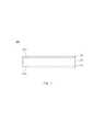
- FIG. 1illustrates a schematic diagram of a dual-mode touch sensing apparatus according to a preferred embodiment of the present invention
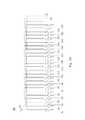
- FIG. 2illustrates a schematic diagram of a projected capacitive touch sensing electrode according to a preferred embodiment of the present invention
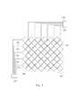
- FIG. 3Aillustrates a schematic diagram of an X-direction antenna loop according to an embodiment of the present invention
- FIG. 3Billustrates a schematic diagram of a Y-direction antenna loop according to an embodiment of the present invention.
- FIG. 4illustrates a schematic diagram that a Y-direction antenna loop of an electromagnetic touch sensing antenna is integrated into an X-direction touch sensing electrode layer of a capacitive touch sensing electrode.
- FIG. 1illustrates a schematic diagram of a dual-mode touch sensing apparatus according to a preferred embodiment of the present invention.
- the dual-mode touch sensing apparatus 100includes a substrate 101 , a capacitive touch sensing electrode 102 and an electromagnetic touch sensing antenna 103 .
- the substrate 101is an ITO (indium tin oxide) glass substrate with a first surface 101 a and a second surface 101 b .
- the capacitive touch sensing electrode 102is formed on the first surface 101 a .
- the electromagnetic touch sensing antenna 103is formed on the second surface 101 b .
- a semiconductor manufacturing processis used to form the capacitive touch sensing electrode 102 on the first surface 101 a .
- the capacitive touch sensing electrode 102is a projected capacitive touch sensing electrode, a surface capacitive touch sensing electrode or another type of capacitive touch sensing electrode.
- the capacitive touch sensing electrode 102is formed as a projected capacitive touch sensing electrode.
- FIG. 2illustrates a schematic diagram of a projected capacitive touch sensing electrode according to a preferred embodiment of the present invention.
- a capacitive touch sensing electrode 102is formed on the first surface 101 a .
- a sputtering methodis used to form a first indium tin oxide (ITO) layer in the first surface 101 a of the substrate 101 .
- a photolithography and etching processis performed on the first indium tin oxide (ITO) layer to form a Y-direction touch sensing electrode layer.
- the Y-direction touch sensing electrode layerincludes a plurality electrode strings 200 which are arranged in parallel to each other in the Y-direction.
- Each Y-direction electrode string 200includes a plurality of rhombus-shaped electrodes 201 arranged in series. Each Y-direction electrode string 200 is connected to a drive line 202 .
- a dielectric layer(not shown in this figure) is formed on the Y-direction touch sensing electrode layer to serve as an insulating layer by a coating method.
- a sputtering methodis used to form a second indium tin oxide (ITO) layer on the dielectric layer.
- a photolithography and etching processis performed on the second indium tin oxide (ITO) layer to form an X-direction touch sensing electrode layer.
- the X-direction touch sensing electrode layerincludes a plurality of electrode strings 210 arranged in parallel to each other and in the X-direction.
- Each X-direction electrode string 210includes a plurality of rhombus-shaped electrodes 211 arranged in series.
- Each X-direction electrode string 210is connected to a drive line 212 .
- the rhombus-shaped electrode 201 and the rhombus-shaped electrode 211are alternately arranged to form the capacitive touch sensing electrode 102 .
- the drive line 202 in the Y-direction and the drive 212 in the X-directionare connected to a controller through connection ports 203 and 213 .
- the controllercan detect the change of capacitance among the capacitive touch sensing electrode 102 to calculate the touch position.
- an electromagnetic touch sensing antenna 103is formed on the second surface 101 b of the substrate 101 after the capacitive touch sensing electrode is finished.
- the electromagnetic touch sensing antenna 103includes a grid antenna composed of a plurality of sensing antennas to sense the change of magnetic flux to calculate the touch position.
- a sputtering methodis used to form a first indium tin oxide (ITO) layer on the second surface 101 b of the substrate 101 .
- a photolithography and etching processis performed on the first indium tin oxide (ITO) layer to form an X-direction antenna loop 300 as illustrated in FIG. 3A .
- the X-direction antenna loop 300includes a plurality of “ ” shaped antennas 301 .
- Two adjacent “ ” shaped antennas 301belong to different sensing loops. Therefore, the touch position can be determined by detecting which “ ” shaped antenna 301 has the change of magnetic flux occurring therein.
- One end of each “ ” shaped antenna 301is connected to a switch, such as a switch X 1 to X 25 , and the other end thereof is connected to a grounded point 303 . Therefore, the magnetic flux of these “ ” shaped antennas 301 can be obtained by sequentially switching the switches X 1 to X 25 .
- a dielectric layer(not shown in this figure) is formed on the X-direction antenna loop 300 to serve as an insulating layer by a coating method.
- a sputtering methodis used to form a second indium tin oxide (ITO) layer on the dielectric layer. Then, a photolithography and etching process is performed on the second indium tin oxide (ITO) layer to form a Y-direction antenna loop 310 as illustrated in FIG. 3B .
- the Y-direction antenna loop 310includes a plurality of “ ” shaped antennas 302 . Two adjacent “ ” shaped antennas 302 belong to different sensing loops. Such structure may help to distinguish which sensing loop happens the electromagnetic induction change. One end of each “ ” shaped antenna 302 is connected to a switch, such as switch Y 1 to Y 25 , and the other end is connected to a grounded point 304 .
- the magnetic flux of these “ ” shaped antennas 302can be obtained by sequentially switching the switches Y 1 to Y 25 . Therefore, the electromagnetic touch sensing antenna 103 is formed on the second surface 101 b .
- the electromagnetic touch sensing antenna 103 and the capacitive touch sensing electrode 102 formed on the first surface 101 aconstitute the dual-mode touch sensing apparatus.
- the capacitive touch sensing electrode 102is formed on the first surface 101 a , and then, the electromagnetic touch sensing antenna 103 is formed on the second surface 101 b to form the dual mode touch sensing apparatus 100 in the above embodiment.
- the electromagnetic touch sensing antenna 103is formed on the second surface 101 b , and then, the capacitive touch sensing electrode 102 is formed on the first surface 101 a to form the dual mode touch sensing apparatus 100 .
- one of the X-direction antenna loop 300 and the Y-direction antenna loop 310 of the electromagnetic touch sensing antenna 10is formed on the first surface 101 a of the substrate 101 . That is, one of the X-direction antenna loop 300 and the Y-direction antenna loop 310 is integrated into the capacitive touch sensing electrode 102 .
- FIG. 4illustrates a schematic diagram that a Y-direction antenna loop of an electromagnetic touch sensing antenna is integrated into an X-direction touch sensing electrode layer of a capacitive touch sensing electrode.
- FIG. 4only the Y-direction antenna loop and X-direction electrode string 210 are illustrated.
- an X-direction antenna loop of an electromagnetic touch sensing antennais integrated into a Y-direction touch sensing electrode layer of a capacitive touch sensing electrode in another embodiment.
- the Y-direction antenna loop 401is disposed between two adjacent X-direction electrode strings 210 .
- each X-direction electrode string 210includes a plurality of rhombus-shaped electrodes 211
- the Y-direction antenna loop 401includes a plurality of sawtooth-shaped antenna segments 402 connected in series and surrounding the rhombus-shaped electrode 211 .
- One end of each sawtooth-shaped antenna segment 402is connected to a switch 404
- the other end of the sawtooth-shaped antenna segment 402is connected to a grounded point 403 . Accordingly, by sequentially switching the switch 404 , a sensing signal is got.
- both the X-direction electrode string 210 and the Y-direction antenna loop 401are formed in same time after an indium tin oxide layer is formed on the substrate. That is, only one mask is needed to form the X-direction electrode string 210 and the Y-direction antenna loop 401 . The process time is much reduced and the cost is also reduced.
- the electromagnetic touch sensing antenna 103is triggered to sense the touch position when a sensing pen touches the dual-mode touch sensing apparatus 100 .
- the electromagnetic touch sensing antenna 103is forced into a low scan frequency operation state when a finger touches the dual-mode touch sensing apparatus 100 . That is, in this case, the capacitive touch sensing electrode 102 is triggered to sense the touch position.
- the electromagnetic touch sensing antenna 103 and the capacitive touch sensing electrode 102are triggered at the same time.
- An incorrect sensing resulthappens because both the X-direction electrode string 210 and the Y-direction antenna loop 401 are formed together that will cause a coupling effect of electrical field.
- a control switch 404is connected to the Y-direction antenna loop 401 .
- the control switch 404is turned off to stop the operation of the electromagnetic touch sensing antenna 103 .
- the control switch 404is turned off to stop the operation of the electromagnetic touch sensing antenna 103 . Therefore, only the capacitive touch sensing electrode 102 is triggered to sense the touch position to prevent interference from the electromagnetic touch sensing antenna 103 .
- the Y-direction antenna loop 401surrounds the X-direction electrode string 210 , the Y-direction antenna loop 401 acts as an electrostatic protection circuit.
- the switch 404is turned on to trigger the Y-direction antenna loop 401 .
- the Y-direction antenna loop 401works with the X-direction antenna loop 402 formed on the other side of the substrate to form a XY antenna loop to sense the touch position.
- the capacitive touch sensing electrode and the electromagnetic touch sensing antennaare formed on the same substrate to form a dual-mode touch sensing apparatus. Therefore, the whole volume of the dual-mode touch sensing apparatus is much reduced.
Landscapes
- Engineering & Computer Science (AREA)
- General Engineering & Computer Science (AREA)
- Theoretical Computer Science (AREA)
- Physics & Mathematics (AREA)
- Human Computer Interaction (AREA)
- General Physics & Mathematics (AREA)
- Electromagnetism (AREA)
- Switches That Are Operated By Magnetic Or Electric Fields (AREA)
- Position Input By Displaying (AREA)
Abstract
Description
- This application claims priority to Taiwan Application Serial Number 101101971, filed Jan. 18, 2012, which is herein incorporated by reference.
- 1. Field of Invention
- The present invention relates to a touch sensing apparatus, and more particularly to a dual-mode touch sensing apparatus with capacitive and electromagnetic sense technology.
- 2. Description of Related Art
- A dual-mode touch sensing apparatus simultaneously includes a capacitive touch sensing electrode and an electromagnetic touch sensing antenna. When the dual-mode touch sensing apparatus is integrated into a liquid crystal display, the capacitive touch sensing electrode and the electromagnetic touch sensing antenna are disposed in different sides of the Liquid crystal display.
- Typically, the electromagnetic sensing antenna is an antenna array formed in a substrate. A control circuit calculates a touch position when a sensing pen touches the electromagnetic sensing antenna. The sensing pen is a transceiver and the substrate with the antenna array is a receiver. When a user uses the sensing pen to touch the substrate, magnetic flux is changed. A control circuit can detect the change of the magnetic flux to calculate the touch position.
- Typically, the electromagnetic sensing antenna is adhered to a backside of the liquid crystal display by an adhering process. That is, an additional adhering process is required. It is not beneficial for the cost. Moreover, if the material of the backside board of the liquid crystal display is metal, the sensing of the electromagnetic sensing antenna will be interfered by the metal backside board, thus affecting the sensing operation. On the other hand, the electromagnetic sensing antenna also increases the whole volume of the liquid crystal display:
- By forming a capacitive touch sensing electrode and an electromagnetic touch sensing antenna on the same substrate, the whole volume of a dual-mode touch sensing apparatus is much reduced.
- The present invention provides a dual-mode touch sensing apparatus. The dual-mode touch sensing apparatus includes a substrate, a first touch sensing electrode formed on the substrate and a second touch sensing electrode formed on the substrate. The first touch sensing electrode is used to perform the capacitive touch sensing technology. The second touch sensing electrode is used to perform the electromagnetic touch sensing technology.
- In an embodiment, the first touch sensing electrode is a projected capacitive touch sensing electrode and formed on a first surface of the substrate, and the second touch sensing electrode is an electromagnetic touch sensing antenna and formed in a second surface of the substrate.
- In an embodiment, a switch circuit is coupled with the electromagnetic touch sensing antenna, and when the projected capacitive touch sensing electrode is operated, the switch circuit is turned off to stop an operation of the electromagnetic touch sensing loop.
- In an embodiment, the projected capacitive touch sensing electrode further comprises a first-direction sensing electrode layer located on the first surface of the substrate, an insulation layer located on the first-direction sensing electrode layer and a second-direction sensing electrode layer located on the insulation layer. The first-direction sensing electrode layer further comprises a plurality of first electrode strings which are arranged in parallel along a first direction, and each of the first electrode strings includes a plurality of first rhombus-shaped electrodes arranged in series. The second-direction sensing electrode layer further comprises a plurality of second electrode strings which are arranged in parallel along a second direction, and each of the second electrode strings includes a plurality of second rhombus-shaped electrodes arranged in series. The first rhombus-shaped electrodes and the second rhombus-shaped electrodes are alternately arranged.
- In an embodiment, the electromagnetic touch sensing antenna further comprises a first-direction antenna loop located on the second surface of the substrate, an insulation layer located on the first-direction antenna loop, and a second-direction antenna loop located on the insulation layer. The first-direction antenna loop further comprises a plurality of “” shaped first antenna segments. Two adjacent first antenna segments belong to different sensing loops. The second-direction antenna loop further comprises a plurality of “
 ” shaped second antenna segments, wherein two adjacent second antenna segments belong to different sensing loops.
 - In an embodiment, the first touch sensing electrode is a projected capacitive touch sensing electrode and formed on a first surface of the substrate, and the second touch sensing electrode is an electromagnetic touch sensing antenna and formed on the first surface and a second surface of the substrate.
- In an embodiment, the projected capacitive touch sensing electrode further comprises a first-direction sensing electrode layer located on the first surface of the substrate, a first insulation layer located on the first-direction sensing electrode layer and a second-direction sensing electrode layer located on the insulation layer. The first-direction sensing electrode layer further comprises a plurality of first electrode strings which are arranged in parallel along a first direction, and each of the first electrode strings includes a plurality of first rhombus-shaped electrodes arranged in series. The second-direction sensing electrode layer further comprises a plurality of second electrode strings which are arranged in parallel along a second direction. Each of the second electrode strings includes a plurality of second rhombus-shaped electrodes arranged in series. The first rhombus-shaped electrodes and the second rhombus-shaped electrodes are alternately arranged.
- In an embodiment, the electromagnetic touch sensing antenna further comprises a first-direction antenna loop located on the second surface of the substrate, a second insulation layer located on the first-direction antenna loop and a second-direction antenna loop located on the first surface. The first-direction antenna loop further comprises a plurality of first antenna segments. Two adjacent first antenna segments belong to different sensing loops. The second-direction antenna loop further comprises a plurality of second sawtooth shaped antenna segments, and each of the sawtooth shaped antenna segments surrounds correspondingly the first electrode string.
- In an embodiment, the electromagnetic touch sensing antenna further comprises a second-direction antenna loop located on the second surface, a second insulation layer located on the second-direction antenna loop and a first-direction antenna loop located on the first insulation layer. The second-direction antenna loop further comprises a plurality of second antenna segment. Two adjacent second antenna segments belong to different sensing loop. The first-direction antenna loop further comprises a plurality of sawtooth shaped antenna segment. Each sawtooth shaped antenna segment surrounds corresponding the second electrode string.
- Accordingly, the capacitive touch sensing electrode and the electromagnetic touch sensing antenna loop are formed on the same substrate to form a dual-mode touch sensing apparatus. Therefore, the whole volume of the dual-mode touch sensing apparatus is much reduced.
- In order to make the foregoing as well as other aspects, features, advantages, and embodiments of the present invention more apparent, the accompanying drawings are described as follows:
FIG. 1 illustrates a schematic diagram of a dual-mode touch sensing apparatus according to a preferred embodiment of the present invention;FIG. 2 illustrates a schematic diagram of a projected capacitive touch sensing electrode according to a preferred embodiment of the present invention;FIG. 3A illustrates a schematic diagram of an X-direction antenna loop according to an embodiment of the present invention;FIG. 3B illustrates a schematic diagram of a Y-direction antenna loop according to an embodiment of the present invention; andFIG. 4 illustrates a schematic diagram that a Y-direction antenna loop of an electromagnetic touch sensing antenna is integrated into an X-direction touch sensing electrode layer of a capacitive touch sensing electrode.- Reference will now be made in detail to the present embodiments of the invention, examples of which are illustrated in the accompanying drawings. Wherever possible, the same reference numbers are used in the drawings and the description to refer to the same or like parts.
FIG. 1 illustrates a schematic diagram of a dual-mode touch sensing apparatus according to a preferred embodiment of the present invention. The dual-modetouch sensing apparatus 100 includes asubstrate 101, a capacitivetouch sensing electrode 102 and an electromagnetictouch sensing antenna 103. In an embodiment, thesubstrate 101 is an ITO (indium tin oxide) glass substrate with a first surface101aand asecond surface 101b. The capacitivetouch sensing electrode 102 is formed on the first surface101a. The electromagnetictouch sensing antenna 103 is formed on thesecond surface 101b. A semiconductor manufacturing process is used to form the capacitivetouch sensing electrode 102 on the first surface101a. The capacitivetouch sensing electrode 102 is a projected capacitive touch sensing electrode, a surface capacitive touch sensing electrode or another type of capacitive touch sensing electrode. In this embodiment, the capacitivetouch sensing electrode 102 is formed as a projected capacitive touch sensing electrode.FIG. 2 illustrates a schematic diagram of a projected capacitive touch sensing electrode according to a preferred embodiment of the present invention. In an embodiment, a capacitivetouch sensing electrode 102 is formed on the first surface101a. First, a sputtering method is used to form a first indium tin oxide (ITO) layer in the first surface101aof thesubstrate 101. Then, a photolithography and etching process is performed on the first indium tin oxide (ITO) layer to form a Y-direction touch sensing electrode layer. The Y-direction touch sensing electrode layer includes aplurality electrode strings 200 which are arranged in parallel to each other in the Y-direction. Each Y-direction electrode string 200 includes a plurality of rhombus-shapedelectrodes 201 arranged in series. Each Y-direction electrode string 200 is connected to adrive line 202. Next, a dielectric layer (not shown in this figure) is formed on the Y-direction touch sensing electrode layer to serve as an insulating layer by a coating method. A sputtering method is used to form a second indium tin oxide (ITO) layer on the dielectric layer. Then, a photolithography and etching process is performed on the second indium tin oxide (ITO) layer to form an X-direction touch sensing electrode layer. The X-direction touch sensing electrode layer includes a plurality ofelectrode strings 210 arranged in parallel to each other and in the X-direction. EachX-direction electrode string 210 includes a plurality of rhombus-shapedelectrodes 211 arranged in series. EachX-direction electrode string 210 is connected to adrive line 212. The rhombus-shapedelectrode 201 and the rhombus-shapedelectrode 211 are alternately arranged to form the capacitivetouch sensing electrode 102. Moreover, thedrive line 202 in the Y-direction and thedrive 212 in the X-direction are connected to a controller throughconnection ports touch sensing electrode 102 to calculate the touch position.- Moreover, an electromagnetic
touch sensing antenna 103 is formed on thesecond surface 101bof thesubstrate 101 after the capacitive touch sensing electrode is finished. The electromagnetictouch sensing antenna 103 includes a grid antenna composed of a plurality of sensing antennas to sense the change of magnetic flux to calculate the touch position. In an embodiment, a sputtering method is used to form a first indium tin oxide (ITO) layer on thesecond surface 101bof thesubstrate 101. Then, a photolithography and etching process is performed on the first indium tin oxide (ITO) layer to form anX-direction antenna loop 300 as illustrated inFIG. 3A . TheX-direction antenna loop 300 includes a plurality of “” shapedantennas 301. Two adjacent “” shapedantennas 301 belong to different sensing loops. Therefore, the touch position can be determined by detecting which “” shapedantenna 301 has the change of magnetic flux occurring therein. One end of each “” shapedantenna 301 is connected to a switch, such as a switch X1 to X25, and the other end thereof is connected to a groundedpoint 303. Therefore, the magnetic flux of these “” shapedantennas 301 can be obtained by sequentially switching the switches X1 to X25. Next, a dielectric layer (not shown in this figure) is formed on theX-direction antenna loop 300 to serve as an insulating layer by a coating method. A sputtering method is used to form a second indium tin oxide (ITO) layer on the dielectric layer. Then, a photolithography and etching process is performed on the second indium tin oxide (ITO) layer to form a Y-direction antenna loop 310 as illustrated inFIG. 3B . The Y-direction antenna loop 310 includes a plurality of “” shapedantennas 302. Two adjacent “” shapedantennas 302 belong to different sensing loops. Such structure may help to distinguish which sensing loop happens the electromagnetic induction change. One end of each “” shapedantenna 302 is connected to a switch, such as switch Y1 to Y25, and the other end is connected to a groundedpoint 304. Accordingly, the magnetic flux of these “” shapedantennas 302 can be obtained by sequentially switching the switches Y1 to Y25. Therefore, the electromagnetictouch sensing antenna 103 is formed on thesecond surface 101b. The electromagnetictouch sensing antenna 103 and the capacitivetouch sensing electrode 102 formed on the first surface101aconstitute the dual-mode touch sensing apparatus. - It is noted that the capacitive
touch sensing electrode 102 is formed on the first surface101a, and then, the electromagnetictouch sensing antenna 103 is formed on thesecond surface 101bto form the dual modetouch sensing apparatus 100 in the above embodiment. However, in another embodiment, the electromagnetictouch sensing antenna 103 is formed on thesecond surface 101b, and then, the capacitivetouch sensing electrode 102 is formed on the first surface101ato form the dual modetouch sensing apparatus 100. - Moreover, in another embodiment, one of the
X-direction antenna loop 300 and the Y-direction antenna loop 310 of the electromagnetic touch sensing antenna10 is formed on the first surface101aof thesubstrate 101. That is, one of theX-direction antenna loop 300 and the Y-direction antenna loop 310 is integrated into the capacitivetouch sensing electrode 102. FIG. 4 illustrates a schematic diagram that a Y-direction antenna loop of an electromagnetic touch sensing antenna is integrated into an X-direction touch sensing electrode layer of a capacitive touch sensing electrode. InFIG. 4 , only the Y-direction antenna loop andX-direction electrode string 210 are illustrated. It is noted that an X-direction antenna loop of an electromagnetic touch sensing antenna is integrated into a Y-direction touch sensing electrode layer of a capacitive touch sensing electrode in another embodiment. The Y-direction antenna loop 401 is disposed between two adjacent X-direction electrode strings210. Because eachX-direction electrode string 210 includes a plurality of rhombus-shapedelectrodes 211, the Y-direction antenna loop 401 includes a plurality of sawtooth-shapedantenna segments 402 connected in series and surrounding the rhombus-shapedelectrode 211. One end of each sawtooth-shapedantenna segment 402 is connected to aswitch 404, and the other end of the sawtooth-shapedantenna segment 402 is connected to a groundedpoint 403. Accordingly, by sequentially switching theswitch 404, a sensing signal is got.- Because the material for forming both the
X-direction electrode string 210 and the Y-direction antenna loop 401 is indium tin oxide, both theX-direction electrode string 210 and the Y-direction antenna loop 401 are formed in same time after an indium tin oxide layer is formed on the substrate. That is, only one mask is needed to form theX-direction electrode string 210 and the Y-direction antenna loop 401. The process time is much reduced and the cost is also reduced. - Moreover, only the electromagnetic
touch sensing antenna 103 is triggered to sense the touch position when a sensing pen touches the dual-modetouch sensing apparatus 100. On the other hand, the electromagnetictouch sensing antenna 103 is forced into a low scan frequency operation state when a finger touches the dual-modetouch sensing apparatus 100. That is, in this case, the capacitivetouch sensing electrode 102 is triggered to sense the touch position. - However, when both the sensing pen and the finger touch the dual-mode
touch sensing apparatus 100, the electromagnetictouch sensing antenna 103 and the capacitivetouch sensing electrode 102 are triggered at the same time. An incorrect sensing result happens because both theX-direction electrode string 210 and the Y-direction antenna loop 401 are formed together that will cause a coupling effect of electrical field. For preventing the above case from occurring, acontrol switch 404 is connected to the Y-direction antenna loop 401. When the capacitivetouch sensing electrode 102 is operated, thecontrol switch 404 is turned off to stop the operation of the electromagnetictouch sensing antenna 103. For example, when both the sensing pen and the finger touch the dual-modetouch sensing apparatus 100, thecontrol switch 404 is turned off to stop the operation of the electromagnetictouch sensing antenna 103. Therefore, only the capacitivetouch sensing electrode 102 is triggered to sense the touch position to prevent interference from the electromagnetictouch sensing antenna 103. On the other hand, because the Y-direction antenna loop 401 surrounds theX-direction electrode string 210, the Y-direction antenna loop 401 acts as an electrostatic protection circuit. When a sensing pen touches the dual-mode touch sensing apparatus, theswitch 404 is turned on to trigger the Y-direction antenna loop 401. At this time, the Y-direction antenna loop 401 works with theX-direction antenna loop 402 formed on the other side of the substrate to form a XY antenna loop to sense the touch position. - Accordingly, the capacitive touch sensing electrode and the electromagnetic touch sensing antenna are formed on the same substrate to form a dual-mode touch sensing apparatus. Therefore, the whole volume of the dual-mode touch sensing apparatus is much reduced.
- It will be apparent to those skilled in the art that various modifications and variations can be made to the structure of the present invention without departing from the scope or spirit of the invention. In view of the foregoing, it is intended that the present invention cover modifications and variations of this invention provided they fall within the scope of the following claims.
Claims (12)
1. A dual-mode touch sensing apparatus, comprising:
a substrate;
a first touch sensing electrode formed on the substrate, wherein the first touch sensing electrode is used to perform a first type of touch sensing technology for sensing a touch position; and
a second touch sensing electrode formed on the substrate, wherein the second touch sensing electrode is used to perform a second type of touch sensing technology for sensing a touch position,
wherein the first type touch sensing technology is the capacitive touch sensing technology, and the second type touch sensing technology is the electromagnetic touch sensing technology.
2. The dual-mode touch sensing apparatus ofclaim 1 , wherein the first touch sensing electrode is a projected capacitive touch sensing electrode and is formed on a first surface of the substrate, and the second touch sensing electrode is an electromagnetic touch sensing antenna and is formed on a second surface of the substrate.
3. The dual-mode touch sensing apparatus ofclaim 2 wherein the electromagnetic touch sensing antenna further comprises:
a first-direction antenna loop located on the second surface of the substrate, wherein the first-direction antenna loop further comprises a plurality of “” shaped first antenna segments, wherein two adjacent “” shaped first antenna segments belong to different sensing loop;

an insulation layer located on the first-direction antenna loop; and
a second-direction antenna loop located on the insulation layer, wherein the second-direction antenna loop further comprises a plurality of “” shaped second antenna segments, wherein two adjacent “” shaped second antenna segments belong to different sensing loop.
4. The dual-mode touch sensing apparatus ofclaim 2 , further comprising a switch circuit coupled with the electromagnetic touch sensing antenna, and when the projected capacitive touch sensing electrode is operated, the switch circuit is turned off to stop an operation of the electromagnetic touch sensing antenna.
5. The dual-mode touch sensing apparatus ofclaim 2 , wherein the projected capacitive touch sensing electrode further comprises:
a first-direction sensing electrode layer located on the first surface of the substrate, wherein the first-direction sensing electrode layer further comprises a plurality of first electrode strings which are arranged in parallel along a first direction, each of the first electrode strings including a plurality of first rhombus-shaped electrodes arranged in series;
an insulation layer located on the first-direction sensing electrode layer; and
a second-direction sensing electrode layer located on the insulation layer, wherein the second-direction sensing electrode layer further comprises a plurality of second electrode strings which are arranged in parallel along a second direction, each of the second electrode strings including a plurality of second rhombus-shaped electrodes arranged in series, wherein the first rhombus-shaped electrodes and the second rhombus-shaped electrodes are alternately arranged.
6. The dual-mode touch sensing apparatus ofclaim 5 wherein the electromagnetic touch sensing antenna further comprises:
a first-direction antenna loop located on the second surface of the substrate, wherein the first-direction antenna loop further comprises a plurality of “” shaped first antenna segments, wherein two adjacent “” shaped first antenna segments belong to different sensing loop;
an insulation layer located on the first-direction antenna loop; and
a second-direction antenna loop located on the insulation layer, wherein the second-direction antenna loop further comprises a plurality of “” shaped second antenna segments, wherein two adjacent “” shaped second antenna segments belong to different sensing loop.
7. The dual-mode touch sensing apparatus ofclaim 1 , wherein the first touch sensing electrode is a projected capacitive touch sensing electrode and is formed on a first surface of the substrate, and the second touch sensing electrode is an electromagnetic touch sensing antenna and is formed on the first surface and a second surface of the substrate.
8. The dual-mode touch sensing apparatus ofclaim 7 , wherein the electromagnetic touch sensing antenna further comprises:
a first-direction antenna loop located on the second surface of the substrate, wherein the first-direction antenna loop further comprises a plurality of first antenna segments, wherein two adjacent first antenna segments belong to different sensing loop;
a second insulation layer located on the first-direction antenna loop; and
a second-direction antenna loop located on the first surface, wherein the second-direction antenna loop further comprises a plurality of second sawtooth shaped antenna segments, each of the sawtooth shaped antenna segments surrounding the first electrode string corresponding to the first direction.
9. The dual-mode touch sensing apparatus ofclaim 7 , wherein the electromagnetic touch sensing antenna further comprises:
a second-direction antenna loop located on the second surface, wherein the second-direction antenna loop further comprises a plurality of second antenna segments, wherein two adjacent second antenna segments belong to different sensing loop;
a second insulation layer located on the second-direction antenna loop; and
a first-direction antenna loop located on the first insulation layer, wherein the first-direction antenna loop further comprises a plurality of sawtooth shaped antenna segments, each of the sawtooth shaped antenna segments surrounding the second electrode string corresponding to the second direction.
10. The dual-mode touch sensing apparatus ofclaim 7 , wherein the projected capacitive touch sensing electrode further comprises:
a first-direction sensing electrode layer located on the first surface of the substrate, wherein the first-direction sensing electrode layer further comprises a plurality of first electrode strings which are arranged in parallel along a first direction, each of the first electrode strings includes a plurality of first rhombus-shaped electrodes arranged in series;
a first insulation layer located on the first-direction sensing electrode layer; and
a second-direction sensing electrode layer located on the insulation layer, wherein the second-direction sensing electrode layer further comprises a plurality of second electrode strings which are arranged in parallel along a second direction, each of the second electrode strings including a plurality of second rhombus-shaped electrodes arranged in series, wherein the first rhombus-shaped electrodes and the second rhombus-shaped electrodes are alternately arranged.
11. The dual-mode touch sensing apparatus ofclaim 10 , wherein the electromagnetic touch sensing antenna further comprises:
a first-direction antenna loop located on the second surface of the substrate, wherein the first-direction antenna loop further comprises a plurality of first antenna segments, wherein two adjacent first antenna segments belong to different sensing loop;
a second insulation layer located on the first-direction antenna loop; and
a second-direction antenna loop located on the first surface, wherein the second-direction antenna loop further comprises a plurality of second sawtooth shaped antenna segments, each of the sawtooth shaped antenna segments surrounding the first electrode string corresponding to the first direction.
12. The dual-mode touch sensing apparatus ofclaim 10 , wherein the electromagnetic touch sensing antenna further comprises:
a second-direction antenna loop located on the second surface, wherein the second-direction antenna loop further comprises a plurality of second antenna segments, wherein two adjacent second antenna segments belong to different sensing loop;
a second insulation layer located on the second-direction antenna loop; and
a first-direction antenna loop located on the first insulation layer, wherein the first-direction antenna loop, further comprises a plurality of sawtooth shaped antenna segments, each of the sawtooth shaped antenna segments surrounding the second electrode string corresponding to the second direction.
Applications Claiming Priority (3)
| Application Number | Priority Date | Filing Date | Title |
|---|---|---|---|
| TW101101971ATWI467453B (en) | 2012-01-18 | 2012-01-18 | Dual-mode touch sensing apparatus |
| TW101101971A | 2012-01-18 | ||
| TW101101971 | 2012-01-18 |
Publications (2)
| Publication Number | Publication Date |
|---|---|
| US20130181937A1true US20130181937A1 (en) | 2013-07-18 |
| US8743086B2 US8743086B2 (en) | 2014-06-03 |
Family
ID=48779621
Family Applications (1)
| Application Number | Title | Priority Date | Filing Date |
|---|---|---|---|
| US13/539,500Expired - Fee RelatedUS8743086B2 (en) | 2012-01-18 | 2012-07-02 | Dual-mode touch sensing apparatus |
Country Status (2)
| Country | Link |
|---|---|
| US (1) | US8743086B2 (en) |
| TW (1) | TWI467453B (en) |
Cited By (38)
| Publication number | Priority date | Publication date | Assignee | Title |
|---|---|---|---|---|
| US20140043284A1 (en)* | 2012-08-08 | 2014-02-13 | Lg Display Co., Ltd. | Display device with touch screen and method of driving the same |
| US20140062906A1 (en)* | 2012-09-06 | 2014-03-06 | Electronics And Telecommunications Research Institute | Touch screens and methods of manufacturing the same |
| US20140145982A1 (en)* | 2012-11-29 | 2014-05-29 | Wistron Neweb Corp. | Touch panel and a control method thereof |
| CN103913873A (en)* | 2013-08-07 | 2014-07-09 | 上海天马微电子有限公司 | Liquid crystal panel, display device and scanning method thereof |
| US20150002446A1 (en)* | 2013-06-28 | 2015-01-01 | Synaptics Incorporated | Wireless communication enabling capacitive imaging sensor assembly |
| US20150022483A1 (en)* | 2013-07-16 | 2015-01-22 | Novatek Microelectronics Corp. | Touch display apparatus |
| US20150035789A1 (en)* | 2013-07-31 | 2015-02-05 | Samuel Brunet | Dynamic Configuration Of Touch Sensor Electrode Clusters |
| WO2015023134A1 (en)* | 2013-08-13 | 2015-02-19 | Samsung Electronics Co., Ltd. | Interaction sensing |
| US20150181715A1 (en)* | 2013-12-25 | 2015-06-25 | Hon Hai Precision Industry Co., Ltd. | Method for manufacturing touch panel |
| US20160062501A1 (en)* | 2014-08-29 | 2016-03-03 | Chunghwa Picture Tubes, Ltd. | Touch apparatus |
| US9323384B2 (en)* | 2014-02-10 | 2016-04-26 | Samsung Display Co., Ltd. | Touch sensor substrate and display apparatus having the touch sensor substrate |
| KR101618286B1 (en) | 2015-02-12 | 2016-05-04 | 주식회사 더한 | Display module for capable of detecting capacitive touch and induced electromagnetic field and display apparatus having the same |
| WO2016178498A1 (en)* | 2015-05-04 | 2016-11-10 | Lg Innotek Co., Ltd. | Touch panel |
| KR20160130603A (en)* | 2015-05-04 | 2016-11-14 | 엘지이노텍 주식회사 | Touch panel |
| EP3098699A1 (en)* | 2015-05-08 | 2016-11-30 | Intel Corporation | Display integrated antenna |
| US9513756B1 (en)* | 2015-08-28 | 2016-12-06 | Clover Network, Inc. | Providing near field communication through a touch screen |
| US20160357306A1 (en)* | 2014-11-28 | 2016-12-08 | Boe Technology Group Co., Ltd. | In-cell touch module, its driving method, touch display panel and display device |
| CN106415458A (en)* | 2014-06-09 | 2017-02-15 | 得翰株式会社 | Multi-input pad for simultaneously sensing capacitive touch and induced electromagnetic field input and input system |
| US20170108972A1 (en)* | 2015-10-16 | 2017-04-20 | Japan Display Inc. | Display apparatus |
| US20170124364A1 (en)* | 2015-11-03 | 2017-05-04 | Microsoft Technology Licensing, Llc | Non-rotationally symmetric short-range wireless tag |
| US20170123563A1 (en)* | 2015-11-03 | 2017-05-04 | Microsoft Technology Licensing, Llc | Extender object for multi-modal sensing |
| US20170123561A1 (en)* | 2015-11-03 | 2017-05-04 | Microsoft Technology Licensing, Llc | User input comprising an event and detected motion |
| US9830012B2 (en)* | 2013-03-13 | 2017-11-28 | Beijing Boe Optoelectronics Technology Co., Ltd. | Touch module and manufacture method thereof |
| US9914066B2 (en) | 2016-03-07 | 2018-03-13 | Microsoft Technology Licensing, Llc | Electromagnetically coupled building blocks |
| US10042446B2 (en) | 2013-08-13 | 2018-08-07 | Samsung Electronics Company, Ltd. | Interaction modes for object-device interactions |
| US20180246608A1 (en)* | 2017-02-28 | 2018-08-30 | Dongwoo Fine-Chem Co., Ltd. | Digitizer and method of preparing the same |
| US10073578B2 (en) | 2013-08-13 | 2018-09-11 | Samsung Electronics Company, Ltd | Electromagnetic interference signal detection |
| US10101869B2 (en) | 2013-08-13 | 2018-10-16 | Samsung Electronics Company, Ltd. | Identifying device associated with touch event |
| US10129432B2 (en) | 2014-11-02 | 2018-11-13 | Clover Network, Inc. | Point of sale platform and associated methods |
| US10141929B2 (en) | 2013-08-13 | 2018-11-27 | Samsung Electronics Company, Ltd. | Processing electromagnetic interference signal using machine learning |
| US10338753B2 (en) | 2015-11-03 | 2019-07-02 | Microsoft Technology Licensing, Llc | Flexible multi-layer sensing surface |
| US10345966B2 (en)* | 2013-09-13 | 2019-07-09 | Lg Display Co., Ltd. | Touch integrated circuit using time-division and touch screen display device including the same |
| CN110580118A (en)* | 2019-09-09 | 2019-12-17 | 上海中航光电子有限公司 | Electromagnetic touch display panel, driving method, and display device |
| US10649572B2 (en)* | 2015-11-03 | 2020-05-12 | Microsoft Technology Licensing, Llc | Multi-modal sensing surface |
| TWI699686B (en)* | 2019-06-21 | 2020-07-21 | 星河半導體股份有限公司 | Touch system and method having dual mode of capacitive and electromagnetic sensing mechanism |
| WO2020147387A1 (en)* | 2019-01-16 | 2020-07-23 | 北京汉王鹏泰科技股份有限公司 | Touch-control sensing unit, touch-control panel, and touch-control display apparatus and method |
| WO2021162379A1 (en)* | 2020-02-14 | 2021-08-19 | 동우화인켐 주식회사 | Electrode structure in which antenna is inserted, and image display device including same |
| US20210314011A1 (en)* | 2020-04-03 | 2021-10-07 | Electronics And Telecommunications Research Institute | Communication device, operation method thereof, and communication system including the same |
Families Citing this family (4)
| Publication number | Priority date | Publication date | Assignee | Title |
|---|---|---|---|---|
| US8933902B2 (en)* | 2012-08-13 | 2015-01-13 | Htc Corporation | Touch panel structure, touch and display panel structure, and integrated touch display panel structure having antenna pattern and method of forming touch panel having antenna pattern |
| CN104571772A (en)* | 2013-10-12 | 2015-04-29 | 上海和辉光电有限公司 | Electromagnetic touch screen structure |
| KR102174679B1 (en)* | 2013-12-31 | 2020-11-06 | 엘지디스플레이 주식회사 | Touch panel |
| KR20180099121A (en)* | 2017-02-28 | 2018-09-05 | 동우 화인켐 주식회사 | Digitizer and Method of Preparing the Same |
Citations (5)
| Publication number | Priority date | Publication date | Assignee | Title |
|---|---|---|---|---|
| US20020053474A1 (en)* | 1999-11-01 | 2002-05-09 | Ching-Chuan Chao | N-shaped antenna loops of digitizer tablet for reducing antenna switches and the method for locating the cordless pen |
| US20060109252A1 (en)* | 2004-11-23 | 2006-05-25 | Microsoft Corporation | Reducing accidental touch-sensitive device activation |
| US20090207150A1 (en)* | 2006-06-21 | 2009-08-20 | Katsuhito Obi | Information processing apparatus, position detecting apparatus and sensing part for performing a detection operation |
| US20090255737A1 (en)* | 2008-03-19 | 2009-10-15 | Egalax_Empia Technology Inc. | Device and Method for Preventing the Influence of Conducting Material from Point Detection of Projected Capacitive Touch Panel |
| US20090267905A1 (en)* | 2008-04-26 | 2009-10-29 | Chung-Wen Hsu | Cursor Input Device With Dual Input Modes |
Family Cites Families (9)
| Publication number | Priority date | Publication date | Assignee | Title |
|---|---|---|---|---|
| KR100459230B1 (en) | 2002-11-14 | 2004-12-03 | 엘지.필립스 엘시디 주식회사 | touch panel for display device |
| KR100480823B1 (en) | 2002-11-14 | 2005-04-07 | 엘지.필립스 엘시디 주식회사 | touch panel for display device |
| TWM329825U (en) | 2007-09-07 | 2008-04-01 | Mildex Optical Inc | Resistance and capacitance integrated touch panel with high flatness |
| TW200915820A (en) | 2007-09-19 | 2009-04-01 | Giga Byte Tech Co Ltd | Touch panel structure having dual touch-modes, and signal processing method and device |
| TWM344520U (en) | 2007-12-06 | 2008-11-11 | Tekom Technologies Inc | Two-in-one touch-control panel |
| JP5094376B2 (en)* | 2007-12-28 | 2012-12-12 | 株式会社ワコム | Position detection device |
| US20100328249A1 (en)* | 2009-06-25 | 2010-12-30 | Stmicroelecronics Asia Pacific Pte Ltd. | Capacitive-inductive touch screen |
| TW201128509A (en)* | 2010-02-11 | 2011-08-16 | Polostar Technology Corp | Signal sensing stucture for touch panel |
| CN102163112B (en)* | 2011-04-07 | 2014-07-23 | 台均科技(深圳)有限公司 | Sensor, dual-mode touch module and dual-mode touch electronic device |
- 2012
- 2012-01-18TWTW101101971Apatent/TWI467453B/ennot_activeIP Right Cessation
- 2012-07-02USUS13/539,500patent/US8743086B2/ennot_activeExpired - Fee Related
Patent Citations (5)
| Publication number | Priority date | Publication date | Assignee | Title |
|---|---|---|---|---|
| US20020053474A1 (en)* | 1999-11-01 | 2002-05-09 | Ching-Chuan Chao | N-shaped antenna loops of digitizer tablet for reducing antenna switches and the method for locating the cordless pen |
| US20060109252A1 (en)* | 2004-11-23 | 2006-05-25 | Microsoft Corporation | Reducing accidental touch-sensitive device activation |
| US20090207150A1 (en)* | 2006-06-21 | 2009-08-20 | Katsuhito Obi | Information processing apparatus, position detecting apparatus and sensing part for performing a detection operation |
| US20090255737A1 (en)* | 2008-03-19 | 2009-10-15 | Egalax_Empia Technology Inc. | Device and Method for Preventing the Influence of Conducting Material from Point Detection of Projected Capacitive Touch Panel |
| US20090267905A1 (en)* | 2008-04-26 | 2009-10-29 | Chung-Wen Hsu | Cursor Input Device With Dual Input Modes |
Cited By (70)
| Publication number | Priority date | Publication date | Assignee | Title |
|---|---|---|---|---|
| US9619086B2 (en)* | 2012-08-08 | 2017-04-11 | Lg Display Co., Ltd. | Display device with touch screen and method of driving the same |
| US20140043284A1 (en)* | 2012-08-08 | 2014-02-13 | Lg Display Co., Ltd. | Display device with touch screen and method of driving the same |
| US20140062906A1 (en)* | 2012-09-06 | 2014-03-06 | Electronics And Telecommunications Research Institute | Touch screens and methods of manufacturing the same |
| US20140145982A1 (en)* | 2012-11-29 | 2014-05-29 | Wistron Neweb Corp. | Touch panel and a control method thereof |
| US9104263B2 (en)* | 2012-11-29 | 2015-08-11 | Wistron Neweb Corp. | Touch panel and a control method thereof |
| US9830012B2 (en)* | 2013-03-13 | 2017-11-28 | Beijing Boe Optoelectronics Technology Co., Ltd. | Touch module and manufacture method thereof |
| US20150002446A1 (en)* | 2013-06-28 | 2015-01-01 | Synaptics Incorporated | Wireless communication enabling capacitive imaging sensor assembly |
| US20150022483A1 (en)* | 2013-07-16 | 2015-01-22 | Novatek Microelectronics Corp. | Touch display apparatus |
| US20150035789A1 (en)* | 2013-07-31 | 2015-02-05 | Samuel Brunet | Dynamic Configuration Of Touch Sensor Electrode Clusters |
| US9874980B2 (en)* | 2013-07-31 | 2018-01-23 | Atmel Corporation | Dynamic configuration of touch sensor electrode clusters |
| US10037119B2 (en) | 2013-07-31 | 2018-07-31 | Atmel Corporation | Dynamic configuration of touch sensor electrode clusters |
| CN103913873A (en)* | 2013-08-07 | 2014-07-09 | 上海天马微电子有限公司 | Liquid crystal panel, display device and scanning method thereof |
| EP2880516A4 (en)* | 2013-08-13 | 2016-01-27 | Samsung Electronics Co Ltd | DETECTION OF INTERACTIONS |
| US10101869B2 (en) | 2013-08-13 | 2018-10-16 | Samsung Electronics Company, Ltd. | Identifying device associated with touch event |
| WO2015023134A1 (en)* | 2013-08-13 | 2015-02-19 | Samsung Electronics Co., Ltd. | Interaction sensing |
| US20150048846A1 (en)* | 2013-08-13 | 2015-02-19 | Samsung Electronics Company, Ltd. | Interaction Sensing |
| JP2016509304A (en)* | 2013-08-13 | 2016-03-24 | サムスン エレクトロニクス カンパニー リミテッド | Interaction sensing |
| CN104969157A (en)* | 2013-08-13 | 2015-10-07 | 三星电子株式会社 | interactive sensing |
| US10318090B2 (en) | 2013-08-13 | 2019-06-11 | Samsung Electronics Company, Ltd. | Interaction sensing |
| US10141929B2 (en) | 2013-08-13 | 2018-11-27 | Samsung Electronics Company, Ltd. | Processing electromagnetic interference signal using machine learning |
| US10108305B2 (en)* | 2013-08-13 | 2018-10-23 | Samsung Electronics Company, Ltd. | Interaction sensing |
| EP2883128A4 (en)* | 2013-08-13 | 2016-01-20 | Samsung Electronics Co Ltd | INTERACTION DETECTION |
| US10073578B2 (en) | 2013-08-13 | 2018-09-11 | Samsung Electronics Company, Ltd | Electromagnetic interference signal detection |
| US10042504B2 (en) | 2013-08-13 | 2018-08-07 | Samsung Electronics Company, Ltd. | Interaction sensing |
| US10042446B2 (en) | 2013-08-13 | 2018-08-07 | Samsung Electronics Company, Ltd. | Interaction modes for object-device interactions |
| US9569055B2 (en) | 2013-08-13 | 2017-02-14 | Samsung Electronics Company, Ltd. | Interaction sensing |
| US10345966B2 (en)* | 2013-09-13 | 2019-07-09 | Lg Display Co., Ltd. | Touch integrated circuit using time-division and touch screen display device including the same |
| US20150181715A1 (en)* | 2013-12-25 | 2015-06-25 | Hon Hai Precision Industry Co., Ltd. | Method for manufacturing touch panel |
| US9179550B2 (en)* | 2013-12-25 | 2015-11-03 | Shenzhen Goldsun Network Intelligence Technology Co., Ltd. | Method for manufacturing touch panel |
| US9323384B2 (en)* | 2014-02-10 | 2016-04-26 | Samsung Display Co., Ltd. | Touch sensor substrate and display apparatus having the touch sensor substrate |
| CN106415458A (en)* | 2014-06-09 | 2017-02-15 | 得翰株式会社 | Multi-input pad for simultaneously sensing capacitive touch and induced electromagnetic field input and input system |
| US20170123569A1 (en)* | 2014-06-09 | 2017-05-04 | The Han Inc. | Multi-input pad for simultaneously sensing capacitive touch and induced electromagnetic field input and input system |
| US20160062501A1 (en)* | 2014-08-29 | 2016-03-03 | Chunghwa Picture Tubes, Ltd. | Touch apparatus |
| US9552116B2 (en)* | 2014-08-29 | 2017-01-24 | Chunghwa Picture Tubes, Ltd. | Touch apparatus |
| US10129432B2 (en) | 2014-11-02 | 2018-11-13 | Clover Network, Inc. | Point of sale platform and associated methods |
| US20160357306A1 (en)* | 2014-11-28 | 2016-12-08 | Boe Technology Group Co., Ltd. | In-cell touch module, its driving method, touch display panel and display device |
| US9904406B2 (en)* | 2014-11-28 | 2018-02-27 | Boe Technology Group Co., Ltd. | In-cell touch module, its driving method, touch display panel and display device |
| KR101618286B1 (en) | 2015-02-12 | 2016-05-04 | 주식회사 더한 | Display module for capable of detecting capacitive touch and induced electromagnetic field and display apparatus having the same |
| KR20160130603A (en)* | 2015-05-04 | 2016-11-14 | 엘지이노텍 주식회사 | Touch panel |
| US20180120971A1 (en)* | 2015-05-04 | 2018-05-03 | Lg Innotek Co., Ltd. | Touch panel |
| KR102286210B1 (en)* | 2015-05-04 | 2021-08-05 | 엘지이노텍 주식회사 | Touch panel |
| US10534483B2 (en) | 2015-05-04 | 2020-01-14 | Lg Innotek Co., Ltd. | Touch panel |
| WO2016178498A1 (en)* | 2015-05-04 | 2016-11-10 | Lg Innotek Co., Ltd. | Touch panel |
| CN107533411A (en)* | 2015-05-04 | 2018-01-02 | Lg伊诺特有限公司 | touch panel |
| EP3098699A1 (en)* | 2015-05-08 | 2016-11-30 | Intel Corporation | Display integrated antenna |
| US10551949B2 (en) | 2015-05-08 | 2020-02-04 | Intel Corporation | Display integrated antenna |
| US10345958B2 (en) | 2015-08-28 | 2019-07-09 | Clover Network, Inc. | Providing near field communication through a touch screen |
| US9851843B2 (en) | 2015-08-28 | 2017-12-26 | Clover Network, Inc. | Providing near field communication through a touch screen |
| US9513756B1 (en)* | 2015-08-28 | 2016-12-06 | Clover Network, Inc. | Providing near field communication through a touch screen |
| US10627933B2 (en)* | 2015-10-16 | 2020-04-21 | Japan Display Inc. | Display apparatus |
| US20170108972A1 (en)* | 2015-10-16 | 2017-04-20 | Japan Display Inc. | Display apparatus |
| US9933891B2 (en)* | 2015-11-03 | 2018-04-03 | Microsoft Technology Licensing, Llc | User input comprising an event and detected motion |
| US10649572B2 (en)* | 2015-11-03 | 2020-05-12 | Microsoft Technology Licensing, Llc | Multi-modal sensing surface |
| US20170124364A1 (en)* | 2015-11-03 | 2017-05-04 | Microsoft Technology Licensing, Llc | Non-rotationally symmetric short-range wireless tag |
| US20170123563A1 (en)* | 2015-11-03 | 2017-05-04 | Microsoft Technology Licensing, Llc | Extender object for multi-modal sensing |
| US20170123561A1 (en)* | 2015-11-03 | 2017-05-04 | Microsoft Technology Licensing, Llc | User input comprising an event and detected motion |
| CN108351981A (en)* | 2015-11-03 | 2018-07-31 | 微软技术许可有限责任公司 | Non-rotationally-symmetric short-distance radio label |
| CN108351733A (en)* | 2015-11-03 | 2018-07-31 | 微软技术许可有限责任公司 | Expander object for multi-modal sensing |
| US10955977B2 (en)* | 2015-11-03 | 2021-03-23 | Microsoft Technology Licensing, Llc | Extender object for multi-modal sensing |
| US10338753B2 (en) | 2015-11-03 | 2019-07-02 | Microsoft Technology Licensing, Llc | Flexible multi-layer sensing surface |
| CN108351731A (en)* | 2015-11-03 | 2018-07-31 | 微软技术许可有限责任公司 | User input including events and detected motion |
| US9914066B2 (en) | 2016-03-07 | 2018-03-13 | Microsoft Technology Licensing, Llc | Electromagnetically coupled building blocks |
| US20180246608A1 (en)* | 2017-02-28 | 2018-08-30 | Dongwoo Fine-Chem Co., Ltd. | Digitizer and method of preparing the same |
| WO2020147387A1 (en)* | 2019-01-16 | 2020-07-23 | 北京汉王鹏泰科技股份有限公司 | Touch-control sensing unit, touch-control panel, and touch-control display apparatus and method |
| TWI699686B (en)* | 2019-06-21 | 2020-07-21 | 星河半導體股份有限公司 | Touch system and method having dual mode of capacitive and electromagnetic sensing mechanism |
| CN110580118A (en)* | 2019-09-09 | 2019-12-17 | 上海中航光电子有限公司 | Electromagnetic touch display panel, driving method, and display device |
| WO2021162379A1 (en)* | 2020-02-14 | 2021-08-19 | 동우화인켐 주식회사 | Electrode structure in which antenna is inserted, and image display device including same |
| US12040535B2 (en) | 2020-02-14 | 2024-07-16 | Dongwoo Fine-Chem Co., Ltd. | Antenna-inserted electrode structure and image display device including the same |
| US20210314011A1 (en)* | 2020-04-03 | 2021-10-07 | Electronics And Telecommunications Research Institute | Communication device, operation method thereof, and communication system including the same |
| US11923882B2 (en)* | 2020-04-03 | 2024-03-05 | Electronics And Telecommunications Research Institute | Communication device, operation method thereof, and communication system including the same |
Also Published As
| Publication number | Publication date |
|---|---|
| TWI467453B (en) | 2015-01-01 |
| TW201331805A (en) | 2013-08-01 |
| US8743086B2 (en) | 2014-06-03 |
Similar Documents
| Publication | Publication Date | Title |
|---|---|---|
| US8743086B2 (en) | Dual-mode touch sensing apparatus | |
| US9606686B2 (en) | Trace shielding for input devices | |
| KR101252230B1 (en) | Capacitive Touch Panel, Manufacturing Method and Scanning Method | |
| US8922501B2 (en) | Capacitive sensing device comprising cross-shaped sensing elements | |
| US9354714B2 (en) | Keypad with integrated touch sensitive apparatus | |
| US9244574B2 (en) | Reducing ion-migration and corrosion in electrodes | |
| CN102541384B (en) | Dual-mode touch control sensor | |
| CN103941933B (en) | Touch display device integrating capacitance and electromagnetic touch | |
| US10852889B2 (en) | Display panel, mobile terminal and driving method | |
| KR101474061B1 (en) | Sensor for detecting proximity/motion and touch and display device having the same | |
| US20090277695A1 (en) | Method of Forming Touch Sensing Circuit Pattern | |
| US20140166611A1 (en) | Electrode structure of the touch panel, method thereof and touch panel | |
| US10126870B2 (en) | Techniques for mitigating noise in capacitive sensing devices | |
| JP2008217784A (en) | Touch panel | |
| US10712863B2 (en) | Transcapacitive touch and force sensing in an input device | |
| US20170045979A1 (en) | Touch Panel and Mobile Terminal | |
| CN106959780B (en) | Touch display panel and touch display device | |
| US9753572B2 (en) | Touch panel, method of fabricating the same and touch display device | |
| CN102622154A (en) | Capacitive touch panel | |
| WO2015080891A1 (en) | Methods and apparatus for arranging electrode layers and associated routing traces in a sensor device | |
| US12189909B2 (en) | Touch substrate, manufacturing method thereof and touch device | |
| CN203812221U (en) | capacitive touchpad | |
| TWM484751U (en) | Capacitive touch panel | |
| CN106796476B (en) | Digitizer sensor | |
| TWI524249B (en) | Capacitive touch panel |
Legal Events
| Date | Code | Title | Description |
|---|---|---|---|
| AS | Assignment | Owner name:CHUNGHWA PICTURE TUBES, LTD., TAIWAN Free format text:ASSIGNMENT OF ASSIGNORS INTEREST;ASSIGNORS:CHEN, YEN-TING;WENG, MING-CHI;CHIU, KUN-CHI;REEL/FRAME:028490/0086 Effective date:20120629 | |
| STCF | Information on status: patent grant | Free format text:PATENTED CASE | |
| FPAY | Fee payment | Year of fee payment:4 | |
| FEPP | Fee payment procedure | Free format text:MAINTENANCE FEE REMINDER MAILED (ORIGINAL EVENT CODE: REM.); ENTITY STATUS OF PATENT OWNER: LARGE ENTITY | |
| LAPS | Lapse for failure to pay maintenance fees | Free format text:PATENT EXPIRED FOR FAILURE TO PAY MAINTENANCE FEES (ORIGINAL EVENT CODE: EXP.); ENTITY STATUS OF PATENT OWNER: LARGE ENTITY | |
| STCH | Information on status: patent discontinuation | Free format text:PATENT EXPIRED DUE TO NONPAYMENT OF MAINTENANCE FEES UNDER 37 CFR 1.362 | |
| FP | Lapsed due to failure to pay maintenance fee | Effective date:20220603 |