US20130170171A1 - Extrusion-based additive manufacturing system for 3d structural electronic, electromagnetic and electromechanical components/devices - Google Patents
Extrusion-based additive manufacturing system for 3d structural electronic, electromagnetic and electromechanical components/devicesDownload PDFInfo
- Publication number
- US20130170171A1 US20130170171A1US13/343,651US201213343651AUS2013170171A1US 20130170171 A1US20130170171 A1US 20130170171A1US 201213343651 AUS201213343651 AUS 201213343651AUS 2013170171 A1US2013170171 A1US 2013170171A1
- Authority
- US
- United States
- Prior art keywords
- machine
- recited
- component
- substrate
- cavities
- Prior art date
- Legal status (The legal status is an assumption and is not a legal conclusion. Google has not performed a legal analysis and makes no representation as to the accuracy of the status listed.)
- Granted
Links
- 238000004519manufacturing processMethods0.000titleclaimsdescription37
- 238000001125extrusionMethods0.000titleclaimsdescription15
- 239000000654additiveSubstances0.000titledescription16
- 230000000996additive effectEffects0.000titledescription16
- 238000000034methodMethods0.000claimsabstractdescription139
- 239000000758substrateSubstances0.000claimsabstractdescription94
- 239000000463materialSubstances0.000claimsabstractdescription69
- 239000004020conductorSubstances0.000claimsabstractdescription41
- 238000000151depositionMethods0.000claimsabstractdescription38
- 238000011049fillingMethods0.000claimsabstractdescription10
- 230000008569processEffects0.000claimsdescription64
- -1PC-ISOPolymers0.000claimsdescription33
- 238000005459micromachiningMethods0.000claimsdescription30
- 238000001723curingMethods0.000claimsdescription22
- 230000008021depositionEffects0.000claimsdescription19
- 238000005520cutting processMethods0.000claimsdescription15
- 238000005516engineering processMethods0.000claimsdescription15
- 238000001459lithographyMethods0.000claimsdescription15
- 229920003229poly(methyl methacrylate)Polymers0.000claimsdescription11
- 239000004926polymethyl methacrylateSubstances0.000claimsdescription11
- 239000012815thermoplastic materialSubstances0.000claimsdescription11
- 229910010293ceramic materialInorganic materials0.000claimsdescription10
- 238000004590computer programMethods0.000claimsdescription10
- 238000005530etchingMethods0.000claimsdescription10
- 229920000106Liquid crystal polymerPolymers0.000claimsdescription8
- 229920000491PolyphenylsulfonePolymers0.000claimsdescription8
- 239000004676acrylonitrile butadiene styreneSubstances0.000claimsdescription8
- 238000000608laser ablationMethods0.000claimsdescription8
- FDPIMTJIUBPUKL-UHFFFAOYSA-Npentan-3-oneChemical compoundCCC(=O)CCFDPIMTJIUBPUKL-UHFFFAOYSA-N0.000claimsdescription8
- 230000010287polarizationEffects0.000claimsdescription8
- 239000002861polymer materialSubstances0.000claimsdescription8
- 239000011347resinSubstances0.000claimsdescription8
- 229920005989resinPolymers0.000claimsdescription8
- 229920003023plasticPolymers0.000claimsdescription7
- 239000004033plasticSubstances0.000claimsdescription7
- 239000004593EpoxySubstances0.000claimsdescription6
- 239000012620biological materialSubstances0.000claimsdescription6
- 239000003990capacitorSubstances0.000claimsdescription6
- 239000011521glassSubstances0.000claimsdescription6
- 238000003754machiningMethods0.000claimsdescription6
- 239000002245particleSubstances0.000claimsdescription6
- 239000004743PolypropyleneSubstances0.000claimsdescription5
- 238000001015X-ray lithographyMethods0.000claimsdescription5
- 238000001816coolingMethods0.000claimsdescription5
- 239000013078crystalSubstances0.000claimsdescription5
- 238000000708deep reactive-ion etchingMethods0.000claimsdescription5
- 230000001419dependent effectEffects0.000claimsdescription5
- 239000003989dielectric materialSubstances0.000claimsdescription5
- 229920001971elastomerPolymers0.000claimsdescription5
- 239000000806elastomerSubstances0.000claimsdescription5
- 238000009760electrical discharge machiningMethods0.000claimsdescription5
- 238000004049embossingMethods0.000claimsdescription5
- 239000006112glass ceramic compositionSubstances0.000claimsdescription5
- 229910010272inorganic materialInorganic materials0.000claimsdescription5
- 239000011147inorganic materialSubstances0.000claimsdescription5
- 229910052500inorganic mineralInorganic materials0.000claimsdescription5
- 239000011810insulating materialSubstances0.000claimsdescription5
- 239000000696magnetic materialSubstances0.000claimsdescription5
- 229910052751metalInorganic materials0.000claimsdescription5
- 239000002184metalSubstances0.000claimsdescription5
- 239000007769metal materialSubstances0.000claimsdescription5
- 239000011707mineralSubstances0.000claimsdescription5
- 239000002086nanomaterialSubstances0.000claimsdescription5
- 239000011368organic materialSubstances0.000claimsdescription5
- 238000001020plasma etchingMethods0.000claimsdescription5
- 239000004632polycaprolactoneSubstances0.000claimsdescription5
- 229920001610polycaprolactonePolymers0.000claimsdescription5
- 229920001155polypropylenePolymers0.000claimsdescription5
- 238000005488sandblastingMethods0.000claimsdescription5
- 239000004065semiconductorSubstances0.000claimsdescription5
- 238000000992sputter etchingMethods0.000claimsdescription5
- 230000032258transportEffects0.000claimsdescription5
- 2380000101463D printingMethods0.000claimsdescription4
- 239000004677NylonSubstances0.000claimsdescription4
- 239000004952PolyamideSubstances0.000claimsdescription4
- 239000005062PolybutadieneSubstances0.000claimsdescription4
- 239000004698PolyethyleneSubstances0.000claimsdescription4
- 239000004642PolyimideSubstances0.000claimsdescription4
- 239000004721Polyphenylene oxideSubstances0.000claimsdescription4
- 239000004793PolystyreneSubstances0.000claimsdescription4
- 229920004798ULTEM® 9085Polymers0.000claimsdescription4
- 229920000122acrylonitrile butadiene styrenePolymers0.000claimsdescription4
- 229920001400block copolymerPolymers0.000claimsdescription4
- 238000006243chemical reactionMethods0.000claimsdescription4
- 229920001940conductive polymerPolymers0.000claimsdescription4
- 229920001577copolymerPolymers0.000claimsdescription4
- 238000004070electrodepositionMethods0.000claimsdescription4
- 229920001903high density polyethylenePolymers0.000claimsdescription4
- 239000004700high-density polyethyleneSubstances0.000claimsdescription4
- 230000001939inductive effectEffects0.000claimsdescription4
- 229910001092metal group alloyInorganic materials0.000claimsdescription4
- 229920001778nylonPolymers0.000claimsdescription4
- 230000003287optical effectEffects0.000claimsdescription4
- 229920000747poly(lactic acid)Polymers0.000claimsdescription4
- 229920002647polyamidePolymers0.000claimsdescription4
- 229920002857polybutadienePolymers0.000claimsdescription4
- 239000004417polycarbonateSubstances0.000claimsdescription4
- 229920000515polycarbonatePolymers0.000claimsdescription4
- 229920000728polyesterPolymers0.000claimsdescription4
- 229920000570polyetherPolymers0.000claimsdescription4
- 229920000139polyethylene terephthalatePolymers0.000claimsdescription4
- 239000005020polyethylene terephthalateSubstances0.000claimsdescription4
- 229920001721polyimidePolymers0.000claimsdescription4
- 229920001470polyketonePolymers0.000claimsdescription4
- 239000004626polylactic acidSubstances0.000claimsdescription4
- 229920000098polyolefinPolymers0.000claimsdescription4
- 229920002223polystyrenePolymers0.000claimsdescription4
- 229920001343polytetrafluoroethylenePolymers0.000claimsdescription4
- 239000004810polytetrafluoroethyleneSubstances0.000claimsdescription4
- 239000011118polyvinyl acetateSubstances0.000claimsdescription4
- 229920002689polyvinyl acetatePolymers0.000claimsdescription4
- 239000004800polyvinyl chlorideSubstances0.000claimsdescription4
- 229920000915polyvinyl chloridePolymers0.000claimsdescription4
- 238000003847radiation curingMethods0.000claimsdescription4
- 229910000679solderInorganic materials0.000claimsdescription4
- 239000007921spraySubstances0.000claimsdescription4
- 238000004544sputter depositionMethods0.000claimsdescription4
- 238000001029thermal curingMethods0.000claimsdescription4
- 229920002397thermoplastic olefinPolymers0.000claimsdescription4
- 238000004891communicationMethods0.000description6
- 238000013461designMethods0.000description5
- 239000000976inkSubstances0.000description5
- BQCADISMDOOEFD-UHFFFAOYSA-NSilverChemical compound[Ag]BQCADISMDOOEFD-UHFFFAOYSA-N0.000description4
- 238000011960computer-aided designMethods0.000description4
- 229910052709silverInorganic materials0.000description4
- 239000004332silverSubstances0.000description4
- 239000007788liquidSubstances0.000description3
- 239000000203mixtureSubstances0.000description3
- 238000004140cleaningMethods0.000description2
- 230000001747exhibiting effectEffects0.000description2
- 238000007667floatingMethods0.000description2
- 230000010354integrationEffects0.000description2
- 238000012544monitoring processMethods0.000description2
- 150000003071polychlorinated biphenylsChemical class0.000description2
- 238000012805post-processingMethods0.000description2
- 239000007787solidSubstances0.000description2
- 239000002904solventSubstances0.000description2
- 239000000126substanceSubstances0.000description2
- 238000012360testing methodMethods0.000description2
- 229920001169thermoplasticPolymers0.000description2
- 239000004416thermosoftening plasticSubstances0.000description2
- 238000002834transmittanceMethods0.000description2
- 230000007723transport mechanismEffects0.000description2
- 239000001993waxSubstances0.000description2
- 229920002494ZeinPolymers0.000description1
- 238000000429assemblyMethods0.000description1
- 230000000712assemblyEffects0.000description1
- 230000005540biological transmissionEffects0.000description1
- 239000003519biomedical and dental materialSubstances0.000description1
- 239000002639bone cementSubstances0.000description1
- 230000000295complement effectEffects0.000description1
- 230000007123defenseEffects0.000description1
- 230000007812deficiencyEffects0.000description1
- 230000001627detrimental effectEffects0.000description1
- 238000011161developmentMethods0.000description1
- 125000003700epoxy groupChemical group0.000description1
- 238000007730finishing processMethods0.000description1
- 239000012530fluidSubstances0.000description1
- 230000004907fluxEffects0.000description1
- 238000005187foamingMethods0.000description1
- 238000010100freeform fabricationMethods0.000description1
- 230000006870functionEffects0.000description1
- 230000036541healthEffects0.000description1
- 239000007943implantSubstances0.000description1
- 150000002739metalsChemical class0.000description1
- 238000012986modificationMethods0.000description1
- 230000004048modificationEffects0.000description1
- 229920000647polyepoxidePolymers0.000description1
- 238000012545processingMethods0.000description1
- 238000011160researchMethods0.000description1
- 238000007711solidificationMethods0.000description1
- 230000008023solidificationEffects0.000description1
- 229920005992thermoplastic resinPolymers0.000description1
- 210000001519tissueAnatomy0.000description1
- XLYOFNOQVPJJNP-UHFFFAOYSA-NwaterSubstancesOXLYOFNOQVPJJNP-UHFFFAOYSA-N0.000description1
- 239000005019zeinSubstances0.000description1
- 229940093612zeinDrugs0.000description1
Images


Classifications
- H—ELECTRICITY
- H01—ELECTRIC ELEMENTS
- H01L—SEMICONDUCTOR DEVICES NOT COVERED BY CLASS H10
- H01L24/00—Arrangements for connecting or disconnecting semiconductor or solid-state bodies; Methods or apparatus related thereto
- H01L24/74—Apparatus for manufacturing arrangements for connecting or disconnecting semiconductor or solid-state bodies
- H01L24/76—Apparatus for connecting with build-up interconnects
- B—PERFORMING OPERATIONS; TRANSPORTING
- B29—WORKING OF PLASTICS; WORKING OF SUBSTANCES IN A PLASTIC STATE IN GENERAL
- B29C—SHAPING OR JOINING OF PLASTICS; SHAPING OF MATERIAL IN A PLASTIC STATE, NOT OTHERWISE PROVIDED FOR; AFTER-TREATMENT OF THE SHAPED PRODUCTS, e.g. REPAIRING
- B29C64/00—Additive manufacturing, i.e. manufacturing of three-dimensional [3D] objects by additive deposition, additive agglomeration or additive layering, e.g. by 3D printing, stereolithography or selective laser sintering
- B29C64/10—Processes of additive manufacturing
- B29C64/106—Processes of additive manufacturing using only liquids or viscous materials, e.g. depositing a continuous bead of viscous material
- B29C64/118—Processes of additive manufacturing using only liquids or viscous materials, e.g. depositing a continuous bead of viscous material using filamentary material being melted, e.g. fused deposition modelling [FDM]
- B—PERFORMING OPERATIONS; TRANSPORTING
- B29—WORKING OF PLASTICS; WORKING OF SUBSTANCES IN A PLASTIC STATE IN GENERAL
- B29C—SHAPING OR JOINING OF PLASTICS; SHAPING OF MATERIAL IN A PLASTIC STATE, NOT OTHERWISE PROVIDED FOR; AFTER-TREATMENT OF THE SHAPED PRODUCTS, e.g. REPAIRING
- B29C64/00—Additive manufacturing, i.e. manufacturing of three-dimensional [3D] objects by additive deposition, additive agglomeration or additive layering, e.g. by 3D printing, stereolithography or selective laser sintering
- B29C64/10—Processes of additive manufacturing
- B29C64/188—Processes of additive manufacturing involving additional operations performed on the added layers, e.g. smoothing, grinding or thickness control
- B—PERFORMING OPERATIONS; TRANSPORTING
- B29—WORKING OF PLASTICS; WORKING OF SUBSTANCES IN A PLASTIC STATE IN GENERAL
- B29C—SHAPING OR JOINING OF PLASTICS; SHAPING OF MATERIAL IN A PLASTIC STATE, NOT OTHERWISE PROVIDED FOR; AFTER-TREATMENT OF THE SHAPED PRODUCTS, e.g. REPAIRING
- B29C70/00—Shaping composites, i.e. plastics material comprising reinforcements, fillers or preformed parts, e.g. inserts
- B29C70/68—Shaping composites, i.e. plastics material comprising reinforcements, fillers or preformed parts, e.g. inserts by incorporating or moulding on preformed parts, e.g. inserts or layers, e.g. foam blocks
- B29C70/72—Encapsulating inserts having non-encapsulated projections, e.g. extremities or terminal portions of electrical components
- B—PERFORMING OPERATIONS; TRANSPORTING
- B33—ADDITIVE MANUFACTURING TECHNOLOGY
- B33Y—ADDITIVE MANUFACTURING, i.e. MANUFACTURING OF THREE-DIMENSIONAL [3-D] OBJECTS BY ADDITIVE DEPOSITION, ADDITIVE AGGLOMERATION OR ADDITIVE LAYERING, e.g. BY 3-D PRINTING, STEREOLITHOGRAPHY OR SELECTIVE LASER SINTERING
- B33Y10/00—Processes of additive manufacturing
- B—PERFORMING OPERATIONS; TRANSPORTING
- B33—ADDITIVE MANUFACTURING TECHNOLOGY
- B33Y—ADDITIVE MANUFACTURING, i.e. MANUFACTURING OF THREE-DIMENSIONAL [3-D] OBJECTS BY ADDITIVE DEPOSITION, ADDITIVE AGGLOMERATION OR ADDITIVE LAYERING, e.g. BY 3-D PRINTING, STEREOLITHOGRAPHY OR SELECTIVE LASER SINTERING
- B33Y70/00—Materials specially adapted for additive manufacturing
- B—PERFORMING OPERATIONS; TRANSPORTING
- B33—ADDITIVE MANUFACTURING TECHNOLOGY
- B33Y—ADDITIVE MANUFACTURING, i.e. MANUFACTURING OF THREE-DIMENSIONAL [3-D] OBJECTS BY ADDITIVE DEPOSITION, ADDITIVE AGGLOMERATION OR ADDITIVE LAYERING, e.g. BY 3-D PRINTING, STEREOLITHOGRAPHY OR SELECTIVE LASER SINTERING
- B33Y80/00—Products made by additive manufacturing
- H—ELECTRICITY
- H01—ELECTRIC ELEMENTS
- H01L—SEMICONDUCTOR DEVICES NOT COVERED BY CLASS H10
- H01L21/00—Processes or apparatus adapted for the manufacture or treatment of semiconductor or solid state devices or of parts thereof
- H01L21/02—Manufacture or treatment of semiconductor devices or of parts thereof
- H01L21/04—Manufacture or treatment of semiconductor devices or of parts thereof the devices having potential barriers, e.g. a PN junction, depletion layer or carrier concentration layer
- H01L21/48—Manufacture or treatment of parts, e.g. containers, prior to assembly of the devices, using processes not provided for in a single one of the groups H01L21/18 - H01L21/326 or H10D48/04 - H10D48/07
- H01L21/4814—Conductive parts
- H01L21/4846—Leads on or in insulating or insulated substrates, e.g. metallisation
- H—ELECTRICITY
- H01—ELECTRIC ELEMENTS
- H01L—SEMICONDUCTOR DEVICES NOT COVERED BY CLASS H10
- H01L24/00—Arrangements for connecting or disconnecting semiconductor or solid-state bodies; Methods or apparatus related thereto
- H01L24/80—Methods for connecting semiconductor or other solid state bodies using means for bonding being attached to, or being formed on, the surface to be connected
- H01L24/82—Methods for connecting semiconductor or other solid state bodies using means for bonding being attached to, or being formed on, the surface to be connected by forming build-up interconnects at chip-level, e.g. for high density interconnects [HDI]
- H—ELECTRICITY
- H05—ELECTRIC TECHNIQUES NOT OTHERWISE PROVIDED FOR
- H05K—PRINTED CIRCUITS; CASINGS OR CONSTRUCTIONAL DETAILS OF ELECTRIC APPARATUS; MANUFACTURE OF ASSEMBLAGES OF ELECTRICAL COMPONENTS
- H05K1/00—Printed circuits
- H05K1/18—Printed circuits structurally associated with non-printed electric components
- H05K1/182—Printed circuits structurally associated with non-printed electric components associated with components mounted in the printed circuit board, e.g. insert mounted components [IMC]
- H05K1/183—Components mounted in and supported by recessed areas of the printed circuit board
- H—ELECTRICITY
- H05—ELECTRIC TECHNIQUES NOT OTHERWISE PROVIDED FOR
- H05K—PRINTED CIRCUITS; CASINGS OR CONSTRUCTIONAL DETAILS OF ELECTRIC APPARATUS; MANUFACTURE OF ASSEMBLAGES OF ELECTRICAL COMPONENTS
- H05K1/00—Printed circuits
- H05K1/18—Printed circuits structurally associated with non-printed electric components
- H05K1/182—Printed circuits structurally associated with non-printed electric components associated with components mounted in the printed circuit board, e.g. insert mounted components [IMC]
- H05K1/185—Components encapsulated in the insulating substrate of the printed circuit or incorporated in internal layers of a multilayer circuit
- H05K1/186—Components encapsulated in the insulating substrate of the printed circuit or incorporated in internal layers of a multilayer circuit manufactured by mounting on or connecting to patterned circuits before or during embedding
- H—ELECTRICITY
- H05—ELECTRIC TECHNIQUES NOT OTHERWISE PROVIDED FOR
- H05K—PRINTED CIRCUITS; CASINGS OR CONSTRUCTIONAL DETAILS OF ELECTRIC APPARATUS; MANUFACTURE OF ASSEMBLAGES OF ELECTRICAL COMPONENTS
- H05K3/00—Apparatus or processes for manufacturing printed circuits
- H05K3/46—Manufacturing multilayer circuits
- H05K3/4644—Manufacturing multilayer circuits by building the multilayer layer by layer, i.e. build-up multilayer circuits
- H05K3/4664—Adding a circuit layer by thick film methods, e.g. printing techniques or by other techniques for making conductive patterns by using pastes, inks or powders
- B—PERFORMING OPERATIONS; TRANSPORTING
- B29—WORKING OF PLASTICS; WORKING OF SUBSTANCES IN A PLASTIC STATE IN GENERAL
- B29C—SHAPING OR JOINING OF PLASTICS; SHAPING OF MATERIAL IN A PLASTIC STATE, NOT OTHERWISE PROVIDED FOR; AFTER-TREATMENT OF THE SHAPED PRODUCTS, e.g. REPAIRING
- B29C2793/00—Shaping techniques involving a cutting or machining operation
- H—ELECTRICITY
- H01—ELECTRIC ELEMENTS
- H01L—SEMICONDUCTOR DEVICES NOT COVERED BY CLASS H10
- H01L21/00—Processes or apparatus adapted for the manufacture or treatment of semiconductor or solid state devices or of parts thereof
- H01L21/02—Manufacture or treatment of semiconductor devices or of parts thereof
- H01L21/04—Manufacture or treatment of semiconductor devices or of parts thereof the devices having potential barriers, e.g. a PN junction, depletion layer or carrier concentration layer
- H01L21/48—Manufacture or treatment of parts, e.g. containers, prior to assembly of the devices, using processes not provided for in a single one of the groups H01L21/18 - H01L21/326 or H10D48/04 - H10D48/07
- H01L21/4814—Conductive parts
- H01L21/4846—Leads on or in insulating or insulated substrates, e.g. metallisation
- H01L21/486—Via connections through the substrate with or without pins
- H—ELECTRICITY
- H01—ELECTRIC ELEMENTS
- H01L—SEMICONDUCTOR DEVICES NOT COVERED BY CLASS H10
- H01L2224/00—Indexing scheme for arrangements for connecting or disconnecting semiconductor or solid-state bodies and methods related thereto as covered by H01L24/00
- H01L2224/01—Means for bonding being attached to, or being formed on, the surface to be connected, e.g. chip-to-package, die-attach, "first-level" interconnects; Manufacturing methods related thereto
- H01L2224/18—High density interconnect [HDI] connectors; Manufacturing methods related thereto
- H01L2224/23—Structure, shape, material or disposition of the high density interconnect connectors after the connecting process
- H01L2224/24—Structure, shape, material or disposition of the high density interconnect connectors after the connecting process of an individual high density interconnect connector
- H01L2224/241—Disposition
- H01L2224/24151—Connecting between a semiconductor or solid-state body and an item not being a semiconductor or solid-state body, e.g. chip-to-substrate, chip-to-passive
- H01L2224/24221—Connecting between a semiconductor or solid-state body and an item not being a semiconductor or solid-state body, e.g. chip-to-substrate, chip-to-passive the body and the item being stacked
- H01L2224/24225—Connecting between a semiconductor or solid-state body and an item not being a semiconductor or solid-state body, e.g. chip-to-substrate, chip-to-passive the body and the item being stacked the item being non-metallic, e.g. insulating substrate with or without metallisation
- H—ELECTRICITY
- H01—ELECTRIC ELEMENTS
- H01L—SEMICONDUCTOR DEVICES NOT COVERED BY CLASS H10
- H01L2224/00—Indexing scheme for arrangements for connecting or disconnecting semiconductor or solid-state bodies and methods related thereto as covered by H01L24/00
- H01L2224/01—Means for bonding being attached to, or being formed on, the surface to be connected, e.g. chip-to-package, die-attach, "first-level" interconnects; Manufacturing methods related thereto
- H01L2224/26—Layer connectors, e.g. plate connectors, solder or adhesive layers; Manufacturing methods related thereto
- H01L2224/31—Structure, shape, material or disposition of the layer connectors after the connecting process
- H01L2224/32—Structure, shape, material or disposition of the layer connectors after the connecting process of an individual layer connector
- H01L2224/321—Disposition
- H01L2224/32151—Disposition the layer connector connecting between a semiconductor or solid-state body and an item not being a semiconductor or solid-state body, e.g. chip-to-substrate, chip-to-passive
- H01L2224/32221—Disposition the layer connector connecting between a semiconductor or solid-state body and an item not being a semiconductor or solid-state body, e.g. chip-to-substrate, chip-to-passive the body and the item being stacked
- H01L2224/32225—Disposition the layer connector connecting between a semiconductor or solid-state body and an item not being a semiconductor or solid-state body, e.g. chip-to-substrate, chip-to-passive the body and the item being stacked the item being non-metallic, e.g. insulating substrate with or without metallisation
- H—ELECTRICITY
- H01—ELECTRIC ELEMENTS
- H01L—SEMICONDUCTOR DEVICES NOT COVERED BY CLASS H10
- H01L2224/00—Indexing scheme for arrangements for connecting or disconnecting semiconductor or solid-state bodies and methods related thereto as covered by H01L24/00
- H01L2224/73—Means for bonding being of different types provided for in two or more of groups H01L2224/10, H01L2224/18, H01L2224/26, H01L2224/34, H01L2224/42, H01L2224/50, H01L2224/63, H01L2224/71
- H01L2224/732—Location after the connecting process
- H01L2224/73251—Location after the connecting process on different surfaces
- H01L2224/73267—Layer and HDI connectors
- H—ELECTRICITY
- H01—ELECTRIC ELEMENTS
- H01L—SEMICONDUCTOR DEVICES NOT COVERED BY CLASS H10
- H01L2224/00—Indexing scheme for arrangements for connecting or disconnecting semiconductor or solid-state bodies and methods related thereto as covered by H01L24/00
- H01L2224/74—Apparatus for manufacturing arrangements for connecting or disconnecting semiconductor or solid-state bodies and for methods related thereto
- H01L2224/75—Apparatus for connecting with bump connectors or layer connectors
- H01L2224/7525—Means for applying energy, e.g. heating means
- H01L2224/75264—Means for applying energy, e.g. heating means by induction heating, i.e. coils
- H—ELECTRICITY
- H01—ELECTRIC ELEMENTS
- H01L—SEMICONDUCTOR DEVICES NOT COVERED BY CLASS H10
- H01L2224/00—Indexing scheme for arrangements for connecting or disconnecting semiconductor or solid-state bodies and methods related thereto as covered by H01L24/00
- H01L2224/74—Apparatus for manufacturing arrangements for connecting or disconnecting semiconductor or solid-state bodies and for methods related thereto
- H01L2224/75—Apparatus for connecting with bump connectors or layer connectors
- H01L2224/7525—Means for applying energy, e.g. heating means
- H01L2224/7528—Resistance welding electrodes, i.e. for ohmic heating
- H—ELECTRICITY
- H01—ELECTRIC ELEMENTS
- H01L—SEMICONDUCTOR DEVICES NOT COVERED BY CLASS H10
- H01L2224/00—Indexing scheme for arrangements for connecting or disconnecting semiconductor or solid-state bodies and methods related thereto as covered by H01L24/00
- H01L2224/74—Apparatus for manufacturing arrangements for connecting or disconnecting semiconductor or solid-state bodies and for methods related thereto
- H01L2224/75—Apparatus for connecting with bump connectors or layer connectors
- H01L2224/7565—Means for transporting the components to be connected
- H—ELECTRICITY
- H01—ELECTRIC ELEMENTS
- H01L—SEMICONDUCTOR DEVICES NOT COVERED BY CLASS H10
- H01L2224/00—Indexing scheme for arrangements for connecting or disconnecting semiconductor or solid-state bodies and methods related thereto as covered by H01L24/00
- H01L2224/74—Apparatus for manufacturing arrangements for connecting or disconnecting semiconductor or solid-state bodies and for methods related thereto
- H01L2224/75—Apparatus for connecting with bump connectors or layer connectors
- H01L2224/759—Means for monitoring the connection process
- H01L2224/75901—Means for monitoring the connection process using a computer, e.g. fully- or semi-automatic bonding
- H—ELECTRICITY
- H01—ELECTRIC ELEMENTS
- H01L—SEMICONDUCTOR DEVICES NOT COVERED BY CLASS H10
- H01L24/00—Arrangements for connecting or disconnecting semiconductor or solid-state bodies; Methods or apparatus related thereto
- H01L24/01—Means for bonding being attached to, or being formed on, the surface to be connected, e.g. chip-to-package, die-attach, "first-level" interconnects; Manufacturing methods related thereto
- H01L24/18—High density interconnect [HDI] connectors; Manufacturing methods related thereto
- H01L24/23—Structure, shape, material or disposition of the high density interconnect connectors after the connecting process
- H01L24/24—Structure, shape, material or disposition of the high density interconnect connectors after the connecting process of an individual high density interconnect connector
- H—ELECTRICITY
- H01—ELECTRIC ELEMENTS
- H01L—SEMICONDUCTOR DEVICES NOT COVERED BY CLASS H10
- H01L24/00—Arrangements for connecting or disconnecting semiconductor or solid-state bodies; Methods or apparatus related thereto
- H01L24/01—Means for bonding being attached to, or being formed on, the surface to be connected, e.g. chip-to-package, die-attach, "first-level" interconnects; Manufacturing methods related thereto
- H01L24/26—Layer connectors, e.g. plate connectors, solder or adhesive layers; Manufacturing methods related thereto
- H01L24/31—Structure, shape, material or disposition of the layer connectors after the connecting process
- H01L24/32—Structure, shape, material or disposition of the layer connectors after the connecting process of an individual layer connector
- H—ELECTRICITY
- H01—ELECTRIC ELEMENTS
- H01L—SEMICONDUCTOR DEVICES NOT COVERED BY CLASS H10
- H01L24/00—Arrangements for connecting or disconnecting semiconductor or solid-state bodies; Methods or apparatus related thereto
- H01L24/73—Means for bonding being of different types provided for in two or more of groups H01L24/10, H01L24/18, H01L24/26, H01L24/34, H01L24/42, H01L24/50, H01L24/63, H01L24/71
- H—ELECTRICITY
- H01—ELECTRIC ELEMENTS
- H01L—SEMICONDUCTOR DEVICES NOT COVERED BY CLASS H10
- H01L24/00—Arrangements for connecting or disconnecting semiconductor or solid-state bodies; Methods or apparatus related thereto
- H01L24/74—Apparatus for manufacturing arrangements for connecting or disconnecting semiconductor or solid-state bodies
- H01L24/75—Apparatus for connecting with bump connectors or layer connectors
- H—ELECTRICITY
- H01—ELECTRIC ELEMENTS
- H01L—SEMICONDUCTOR DEVICES NOT COVERED BY CLASS H10
- H01L2924/00—Indexing scheme for arrangements or methods for connecting or disconnecting semiconductor or solid-state bodies as covered by H01L24/00
- H01L2924/10—Details of semiconductor or other solid state devices to be connected
- H01L2924/11—Device type
- H01L2924/12—Passive devices, e.g. 2 terminal devices
- H01L2924/1204—Optical Diode
- H01L2924/12042—LASER
- H—ELECTRICITY
- H01—ELECTRIC ELEMENTS
- H01L—SEMICONDUCTOR DEVICES NOT COVERED BY CLASS H10
- H01L2924/00—Indexing scheme for arrangements or methods for connecting or disconnecting semiconductor or solid-state bodies as covered by H01L24/00
- H01L2924/10—Details of semiconductor or other solid state devices to be connected
- H01L2924/11—Device type
- H01L2924/13—Discrete devices, e.g. 3 terminal devices
- H01L2924/1301—Thyristor
- H—ELECTRICITY
- H01—ELECTRIC ELEMENTS
- H01L—SEMICONDUCTOR DEVICES NOT COVERED BY CLASS H10
- H01L2924/00—Indexing scheme for arrangements or methods for connecting or disconnecting semiconductor or solid-state bodies as covered by H01L24/00
- H01L2924/10—Details of semiconductor or other solid state devices to be connected
- H01L2924/11—Device type
- H01L2924/14—Integrated circuits
- H01L2924/143—Digital devices
- H01L2924/1434—Memory
- H—ELECTRICITY
- H01—ELECTRIC ELEMENTS
- H01L—SEMICONDUCTOR DEVICES NOT COVERED BY CLASS H10
- H01L2924/00—Indexing scheme for arrangements or methods for connecting or disconnecting semiconductor or solid-state bodies as covered by H01L24/00
- H01L2924/10—Details of semiconductor or other solid state devices to be connected
- H01L2924/146—Mixed devices
- H01L2924/1461—MEMS
- H—ELECTRICITY
- H01—ELECTRIC ELEMENTS
- H01L—SEMICONDUCTOR DEVICES NOT COVERED BY CLASS H10
- H01L2924/00—Indexing scheme for arrangements or methods for connecting or disconnecting semiconductor or solid-state bodies as covered by H01L24/00
- H01L2924/15—Details of package parts other than the semiconductor or other solid state devices to be connected
- H01L2924/151—Die mounting substrate
- H01L2924/1515—Shape
- H01L2924/15153—Shape the die mounting substrate comprising a recess for hosting the device
- H—ELECTRICITY
- H01—ELECTRIC ELEMENTS
- H01L—SEMICONDUCTOR DEVICES NOT COVERED BY CLASS H10
- H01L2924/00—Indexing scheme for arrangements or methods for connecting or disconnecting semiconductor or solid-state bodies as covered by H01L24/00
- H01L2924/15—Details of package parts other than the semiconductor or other solid state devices to be connected
- H01L2924/151—Die mounting substrate
- H01L2924/156—Material
- H01L2924/157—Material with a principal constituent of the material being a metal or a metalloid, e.g. boron [B], silicon [Si], germanium [Ge], arsenic [As], antimony [Sb], tellurium [Te] and polonium [Po], and alloys thereof
- H—ELECTRICITY
- H01—ELECTRIC ELEMENTS
- H01L—SEMICONDUCTOR DEVICES NOT COVERED BY CLASS H10
- H01L2924/00—Indexing scheme for arrangements or methods for connecting or disconnecting semiconductor or solid-state bodies as covered by H01L24/00
- H01L2924/15—Details of package parts other than the semiconductor or other solid state devices to be connected
- H01L2924/151—Die mounting substrate
- H01L2924/156—Material
- H01L2924/15786—Material with a principal constituent of the material being a non metallic, non metalloid inorganic material
- H01L2924/15787—Ceramics, e.g. crystalline carbides, nitrides or oxides
- H—ELECTRICITY
- H01—ELECTRIC ELEMENTS
- H01L—SEMICONDUCTOR DEVICES NOT COVERED BY CLASS H10
- H01L2924/00—Indexing scheme for arrangements or methods for connecting or disconnecting semiconductor or solid-state bodies as covered by H01L24/00
- H01L2924/15—Details of package parts other than the semiconductor or other solid state devices to be connected
- H01L2924/151—Die mounting substrate
- H01L2924/156—Material
- H01L2924/15786—Material with a principal constituent of the material being a non metallic, non metalloid inorganic material
- H01L2924/15788—Glasses, e.g. amorphous oxides, nitrides or fluorides
- H—ELECTRICITY
- H01—ELECTRIC ELEMENTS
- H01L—SEMICONDUCTOR DEVICES NOT COVERED BY CLASS H10
- H01L2924/00—Indexing scheme for arrangements or methods for connecting or disconnecting semiconductor or solid-state bodies as covered by H01L24/00
- H01L2924/15—Details of package parts other than the semiconductor or other solid state devices to be connected
- H01L2924/151—Die mounting substrate
- H01L2924/156—Material
- H01L2924/1579—Material with a principal constituent of the material being a polymer, e.g. polyester, phenolic based polymer, epoxy
- H—ELECTRICITY
- H05—ELECTRIC TECHNIQUES NOT OTHERWISE PROVIDED FOR
- H05K—PRINTED CIRCUITS; CASINGS OR CONSTRUCTIONAL DETAILS OF ELECTRIC APPARATUS; MANUFACTURE OF ASSEMBLAGES OF ELECTRICAL COMPONENTS
- H05K1/00—Printed circuits
- H05K1/02—Details
- H05K1/0272—Adaptations for fluid transport, e.g. channels, holes
- H—ELECTRICITY
- H05—ELECTRIC TECHNIQUES NOT OTHERWISE PROVIDED FOR
- H05K—PRINTED CIRCUITS; CASINGS OR CONSTRUCTIONAL DETAILS OF ELECTRIC APPARATUS; MANUFACTURE OF ASSEMBLAGES OF ELECTRICAL COMPONENTS
- H05K2203/00—Indexing scheme relating to apparatus or processes for manufacturing printed circuits covered by H05K3/00
- H05K2203/02—Details related to mechanical or acoustic processing, e.g. drilling, punching, cutting, using ultrasound
- H05K2203/0228—Cutting, sawing, milling or shearing
- H—ELECTRICITY
- H05—ELECTRIC TECHNIQUES NOT OTHERWISE PROVIDED FOR
- H05K—PRINTED CIRCUITS; CASINGS OR CONSTRUCTIONAL DETAILS OF ELECTRIC APPARATUS; MANUFACTURE OF ASSEMBLAGES OF ELECTRICAL COMPONENTS
- H05K2203/00—Indexing scheme relating to apparatus or processes for manufacturing printed circuits covered by H05K3/00
- H05K2203/12—Using specific substances
- H05K2203/122—Organic non-polymeric compounds, e.g. oil, wax or thiol
- H—ELECTRICITY
- H05—ELECTRIC TECHNIQUES NOT OTHERWISE PROVIDED FOR
- H05K—PRINTED CIRCUITS; CASINGS OR CONSTRUCTIONAL DETAILS OF ELECTRIC APPARATUS; MANUFACTURE OF ASSEMBLAGES OF ELECTRICAL COMPONENTS
- H05K3/00—Apparatus or processes for manufacturing printed circuits
- H05K3/0011—Working of insulating substrates or insulating layers
- H05K3/0044—Mechanical working of the substrate, e.g. drilling or punching
- H—ELECTRICITY
- H05—ELECTRIC TECHNIQUES NOT OTHERWISE PROVIDED FOR
- H05K—PRINTED CIRCUITS; CASINGS OR CONSTRUCTIONAL DETAILS OF ELECTRIC APPARATUS; MANUFACTURE OF ASSEMBLAGES OF ELECTRICAL COMPONENTS
- H05K3/00—Apparatus or processes for manufacturing printed circuits
- H05K3/40—Forming printed elements for providing electric connections to or between printed circuits
- H05K3/4038—Through-connections; Vertical interconnect access [VIA] connections
- H05K3/4053—Through-connections; Vertical interconnect access [VIA] connections by thick-film techniques
- H05K3/4069—Through-connections; Vertical interconnect access [VIA] connections by thick-film techniques for via connections in organic insulating substrates
- Y—GENERAL TAGGING OF NEW TECHNOLOGICAL DEVELOPMENTS; GENERAL TAGGING OF CROSS-SECTIONAL TECHNOLOGIES SPANNING OVER SEVERAL SECTIONS OF THE IPC; TECHNICAL SUBJECTS COVERED BY FORMER USPC CROSS-REFERENCE ART COLLECTIONS [XRACs] AND DIGESTS
- Y10—TECHNICAL SUBJECTS COVERED BY FORMER USPC
- Y10T—TECHNICAL SUBJECTS COVERED BY FORMER US CLASSIFICATION
- Y10T29/00—Metal working
- Y10T29/49—Method of mechanical manufacture
- Y10T29/49002—Electrical device making
- Y10T29/49117—Conductor or circuit manufacturing
- Y10T29/49124—On flat or curved insulated base, e.g., printed circuit, etc.
- Y10T29/4913—Assembling to base an electrical component, e.g., capacitor, etc.
- Y—GENERAL TAGGING OF NEW TECHNOLOGICAL DEVELOPMENTS; GENERAL TAGGING OF CROSS-SECTIONAL TECHNOLOGIES SPANNING OVER SEVERAL SECTIONS OF THE IPC; TECHNICAL SUBJECTS COVERED BY FORMER USPC CROSS-REFERENCE ART COLLECTIONS [XRACs] AND DIGESTS
- Y10—TECHNICAL SUBJECTS COVERED BY FORMER USPC
- Y10T—TECHNICAL SUBJECTS COVERED BY FORMER US CLASSIFICATION
- Y10T29/00—Metal working
- Y10T29/53—Means to assemble or disassemble
- Y10T29/5313—Means to assemble electrical device
- Y10T29/53174—Means to fasten electrical component to wiring board, base, or substrate
Definitions
- the present inventionrelates in general to the manufacture of electronic, electromagnetic and electromechanical components and devices, and more particularly to multiple material fabrication using an extrusion-based additive manufacturing system.
- U.S. Pat. No. 5,121,329 issued to Crump (1992)discloses an apparatus incorporating a movable dispensing head provided with a supply of material which solidifies at a predetermined temperature, and a base member, which are moved relative to each other along “X,” “Y,” and “Z” axes in a predetermined pattern to create three-dimensional objects by building up material discharged from the dispensing head onto the base member at a controlled rate.
- the apparatusis preferably computer driven in a process utilizing computer aided design (CAD) and computer-aided manufacturing (CAM) software to generate drive signals for controlled movement of the dispensing head and base member as material is being dispensed.
- Three-dimensional objectsmay be produced by depositing repeated layers of solidifying material until the shape is formed.
- Each layer baseis defined by the previous layer, and each layer thickness is defined and closely controlled by the height at which the tip of the dispensing head is positioned above the preceding layer.
- the present inventiondescribes an extrusion-based additive manufacturing system for 3D structural electronics that uses an innovative manufacturing process whereby multiple technologies are integrated into a single apparatus, device or machine to produce multi-material, heterogeneous, electronic structures exhibiting non-conventional component placement and sufficient mechanical properties.
- the present inventionprovides a method for making a three-dimensional electronic, electromagnetic or electromechanical component/device by: (1) creating one or more layers of a three-dimensional substrate by depositing a substrate material in a layer-by-layer fashion, wherein the substrate includes a plurality of interconnection cavities and component cavities; (2) filling the interconnection cavities with a conductive material; and (3) placing one or more electronic components in the component cavities. The process can be repeated to create additional layers of the three-dimensional substrate.
- the present inventionalso provides a three-dimensional electronic, electromagnetic or electromechanical component/device made by the foregoing method.
- the present inventionprovides a system for making a three-dimensional electronic, electromagnetic or electromechanical component/device that includes a three-dimensional printing device that creates one or more layers of a three-dimensional substrate by depositing a substrate material in a layer-by-layer fashion, wherein the substrate includes a plurality of interconnection cavities and component cavities.
- a first machinethat fills the interconnection cavities with a conductive material.
- a component placement machinethat places one or more components in the component cavities.
- the systemmay also include a slide, a conveyor or a robotic device that transports the three-dimensional substrate to each machine or sub-system.
- the present inventionprovides a three-dimensional electronic, electromagnetic or electromechanical component/device made by a method comprising the steps of (a) creating one or more layers of a three-dimensional substrate by depositing a substrate material in a layer-by-layer fashion, wherein the substrate includes a plurality of interconnection cavities and component cavities, (b) filling the interconnection cavities with a conductive material, and (c) placing one or more components in the component cavities.
- FIG. 1is a flow chart of a method for making a three-dimensional electronic, electromagnetic or electromechanical component/device in accordance with one embodiment of the present invention
- FIG. 2is a flow chart of a method for making a three-dimensional electronic, electromagnetic or electromechanical component/device in accordance with another embodiment of the present invention
- FIG. 3is a flow chart of method for making a three-dimensional electronic, electromagnetic or electromechanical component/device in accordance with another embodiment of the present invention
- FIGS. 4A-4Cshow FDM-manufactured substrates with laser cut features demonstrating the feasibility of producing interconnection channels and component cavities with laser technologies in accordance with the present invention
- FIGS. 5A-5Cshow a broadband anti-reflection grating and FIG. 5D shows a plot of the structure's performance in terms of electromagnetic reflectance, transmittance and conservation in accordance with various steps of the present invention
- FIGS. 6Ashows a CAD model for a scaled UAV wing and FIGS. 6B-6D show the scaled UAV wing fabricated with an FDM machine in accordance with various steps of the present invention
- FIGS. 7A and 7Bshow a circuit part manufactured with the first two steps of the present invention
- FIG. 8shows a component/device manufactured using the method in accordance with one embodiment of the present invention.
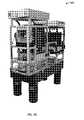
- FIGS. 9A-9Dshow an example of an extrusion-based additive manufacturing system for 3D structural electronic, electromagnetic and electromechanical components/devices in accordance with the present invention.
- One embodiment of the present inventionprovides an extrusion-based additive manufacturing system for 3D structural electronic, electromagnetic and electromechanical components/devices that utilizes fused deposition modeling (FDM), pick and place technology, computer numerical control (CNC) machining to develop an automated process that innovatively fabricates multi-material, heterogeneous, electronic, electromagnetic or electromechanical components/structures/devices without requiring assembly and exhibiting non-conventional component placement and sufficient mechanical properties and other material properties for the application.
- FDMfused deposition modeling
- CNCcomputer numerical control
- Some potentially relevant mechanical and material properties that may be required for the functional productmay include impact resistance, elastic modulus, Poisson's ratio, flexural modulus and strength, tensile strength, creep, fatigue endurance, dielectric strength, dielectric constant, dissipation factor, thermal conductivity, deflection temperature, chemical resistivity, and water absorptivity. Additional processes can also be used as described below.
- additive Manufacturinghas been used in a hybrid stereolithography (SL) and direct write (DW) system that successfully fabricated a LM 555 circuit [5, 6, 8, 9].
- FDMFused deposition modeling
- PCBprinted circuit board
- FDMdirect-write, or direct print
- technologiesare used in the extrusion-based additive manufacturing system for fabricating 3D structural electronics, electromagnetic and electromechanical components/structures/devices.
- micro-machiningsubtractive manufacturing method for the AM-fabricated substrate, which in the case of conventional FDM, is an extruded thermoplastic material.
- Tests conductedhave proven the successful CNC micro-machining of interconnection channels as small as 230 ⁇ m. Laser ablation tests have also been performed and show greater resolutions which may not be possible with current CNC micro-machining Attributes of parts produced by this new invention are applicable in the electronics, electromechanical and biomedical industries.
- extrusion-based additive manufacturing system for 3D structural electronic, electromagnetic and electromechanical components/devicesaddresses both these issues as: 1) parts are fabricated in a layered fashion wherein electronic components can be placed anywhere within a complex 3D part thus resulting in the simultaneous fulfillment of mechanical and electrical design requirements; and 2) parts can be designed and fabricated to possess multi-functions, such as the capability to provide impact resistance and substantial structural support by including stress reducing features (e.g., arches, trusses, filets, etc.) as well as intelligence through the integrated electronics, electromagnetic structures (e.g., gratings, transmission lines, filters, etc.) or electromechanical structures (e.g., actuators, gauges, mechanical sensors, etc.).
- stress reducing featurese.g., arches, trusses, filets, etc.
- electromagnetic structurese.g., gratings, transmission lines, filters, etc.
- electromechanical structurese.g., actuators, gauges, mechanical sensors, etc.
- component and interconnection cavitiesdo not require chemical cleansing as in the case of stereolithography wherein solvents are used to remove uncured photopolymer. This cleaning process is described in [4, 5, 6, 7, 8, 9, 10]. Residual photopolymer and solvent are both detrimental to the quality and reliability of electronic circuits.
- the present inventionsolves the FDM resolution issue by employing subtractive manufacturing methods that are intermittently used during the additive manufacturing process to provide high resolution and accurate features.
- These subtractive manufacturing processesmay include a micro-machining machine, a CNC micro-machining machine, a micro electrical discharge machining machine, an electrochemical machining machine, a direct write proton micro-machining machine, a laser ablation machine, a radiative source, an ultrasonic cutting machine, a hot wire cutting machine, a waterjet machine, an etching machine, a deep reactive ion etching machine, a plasma etching machine, a crystal orientation dependent etching machine, a wet bulk micromachining machine, a UV-lithography or X-ray lithography (LIGA) machine, a hot embossing lithography machine, a precision mechanical sawing machine, a chemically assisted ion milling machine, a sand blasting machine, a cutting machine, or other suitable systems.
- CNC micromachiningcan achieve interconnection channels as small as 230 ⁇ m
- the extrusion-based additive manufacturing system for 3D structural electronicsaddresses the limitations of the planar arrangement in a conventional PCB.
- Non-conventional placement of electronic components in a complex 3D partwill enable the evolution of circuitry design. That is, parts will be limited by designs rather than manufacturing capabilities as is the current state-of-the-art.
- PCBsuse a substrate that provides mechanical stability for component interconnections and require a housing to provide structural support for the entire electronic, electromagnetic or electromechanical component/device.
- the present inventionprovides components/devices with structural support without having to use a housing unless such a housing is desired.
- the extrusion-based additive manufacturing system for 3D structural electronicshas applications in the electronics industry as it promises to dramatically reduce manufacturing cost by, for example, eliminating the requirement of always having a housing to provide structural support.
- Government agenciessuch as the Department of Defense, can use the present invention in a wide variety of applications including, but not limited to: 1) unmanned aerial systems (UASs) or unmanned aerial vehicles (UAVs) by providing aerodynamic parts with embedded sensors, communications and electronics within structural components or by directly fabricating onto UAS and UAV surfaces; 2) customized, mission-specific disposable electronics; 3) truly 3D antennas and photonic devices that improve communications; 4) replacement components for virtually any electronic system on a naval vessel; 5) custom fit sailor-borne electronics and communications systems; and 6) disposable floating depth-specific sensor systems.
- UASsunmanned aerial systems
- UAVsunmanned aerial vehicles
- the inventioncan also be used in structural health monitoring, where 3D electronics are expected to play an important role in the future.
- This inventionwill allow real-time nondestructive monitoring of structural parts where sensors can be strategically placed in a complex part, which is very difficult to do with current manufacturing processes.
- FIG. 1a flow chart of a method 100 for making a three-dimensional electronic, electromagnetic or electromechanical component/device in accordance with one embodiment of the present invention is shown.
- One or more layers of a three-dimensional substrateis/are created by depositing a substrate material in a layer-by-layer fashion in block 102 .
- the substrate materialmay include a thermoplastic material as is typically used in FDM, or alternatively may include another polymer material, a ceramic material, a metallic material, a mineral material, a glass ceramic material, a semi-conductor material, a nanomaterial, a biomaterial, an organic material, an inorganic material, or any combination thereof.
- the substrateincludes a plurality of interconnection cavities and component cavities.
- the thermoplastic materialcan be a material currently used commercially in FDM, such as acrylonitrile butadiene styrene (ABS), ABSi, ABSplus, ABS-M30, ABS-M30i, polycarbonate (PC), PC-ABS, PC-ISO, polyphenylsulfone (PPSF/PPSU), ULTEM 9085, or other material available from the FDM manufacturer; or alternatively, virtually any extrudable material such as poly(methyl methacrylate) (PMMA), polypropylene, polyolefin, LL-PE, HDPE, polyvinyl acetate, polyester, polyamides, nylon, polyimides, polyketone, polyether ethyl ketone (PEEK), polybutadiene, polylactic acid, polycaprolactone, polyethylene terephthalate, liquid crystalline polymer (LCP), polystyrene, polyvinyl chloride, polyfluoroethylene, polydifluoroethylene, polytetrafluoroethylene
- the one or more layerscan be deposited using a three-dimensional printing process, a fused deposition modeling process or other suitable process.
- the interconnection cavitiesmay include an interconnection channel, a pin cavity and/or a via.
- the portion of the substratecan be removed using a micro-machining process, a laser ablation process or other suitable process.
- the interconnection cavitiesare filled with a conductive material in block 104 .
- the conductive materialcan be a metal, a metal alloy, an ink containing conductive particles (e.g., silver particles), a conductive polymer, a wire or other suitable material.
- filling the interconnections cavitiescan be done by inserting, placing or otherwise causing the conductive material (e.g., a liquid, a paste, a wire-bond, a filament, a solid, etc.) to be within the interconnection cavity.
- the interconnection cavitiescan be filled using a direct-write microdispensing process, a direct-print microdispensing process, a fused deposition modeling head, another extrusion-based deposition system, an inkjet dispensing system, a spray machine, a wire bonding machine, a solder machine, a photolithographic technique, an electrodeposition machine, a damascene process, a rotogravure machine, an electro sputtering machine or other suitable process.
- the interconnection cavitiesmay be filled by physically embedding electrical conductors. Subsequently, an ultrasonic staking machine may be used to secure the electrical conductor or components.
- the electronic componentsmay include an electronic component (e.g., an integrated circuit, a resistor, a capacitor, an inductor, a transistor, a thermistor, a thyristor, a sensor, a processor, a memory, an interface device, a display, a power source, an energy conversion device or an antenna), an electrostatic component, a pneumatic component, an electroacoustic component, a microelectromechanical system (MEMS), a biomedical component, an electrochemical component, an electromechanical component, an electromagnetic component, a mechanical component, a metamaterial component, an optical component, a photonic component, a thermal component, a thermal management component, or any other desired component.
- an electronic componente.g., an integrated circuit, a resistor, a capacitor, an inductor, a transistor, a thermistor, a thyristor, a sensor, a processor, a memory, an interface device, a display, a power source, an energy conversion device or an
- the electronic componentscan be placed by hand or by using a component placement machine, such as a pick and place machine, a robotic process or other automated component placement technology.
- the conductive materialis cured.
- the conductive materialcan be cured using a laser, an Ohmic curing process, an inductive curing process, a radiation curing process, a thermal curing process, an electric polarization process or a magnetic polarization process or other suitable process.
- Several of these methods of curingare described in [8, 9, 10, 11] as examples.
- the curingcan be localized or directed to a specific conductive material rather than exposing the entire structure to the extremes necessary for the curing. Localized, high energy fluxes will also ensure an energy efficient process.
- the curing stepcan be eliminated whenever a self-curing conductive material is used.
- the process(blocks 102 , 104 and/or 106 ) can be repeated to create additional layers of the three-dimensional substrate.
- the resulting three-dimensional substrateprovides structural support for the electronic components, and may or may not require a housing for structural support.
- the three-dimensional substratemay include one or more arches, trusses, filets or other stress reducing features.
- the plurality of interconnection cavities and component cavities within the substratecan be created by removing a portion of the substrate using a micro-machining machine, a CNC micro-machining machine, a micro electrical discharge machining machine, an electrochemical machining machine, a direct write proton micro-machining machine, a laser ablation machine, a radiative source, an ultrasonic cutting machine, a hot wire cutting machine, a waterjet machine, an etching machine, a deep reactive ion etching machine, a plasma etching machine, a crystal orientation dependent etching machine, a wet bulk micromachining machine, a UV-lithography or X-ray lithography (LIGA) machine, a hot embossing lithography machine, a precision mechanical sawing machine, a chemically assisted ion milling machine, a sand blasting machine, a cutting machine, or other suitable systems.
- LIGAUV-lithography or X-ray lithography
- FIGS. 4A-4Cshow FDM-manufactured substrates with laser cut features demonstrating the feasibility of producing interconnection channels and component cavities with laser technologies.
- a portion of the substratecan be removed for a diffraction grating, an electromagnetically responsive structure, a cooling channel, a vent or any other desired structure.
- FIGS. 5A-5Cshow a broadband anti-reflection grating and FIG. 5D shows a plot of the structure's performance in terms of electromagnetic reflectance, transmittance and conservation.
- the processmay also include the step of depositing a thermally conductive material, a ceramic material, a dielectric material, a magnetic material, a piezoelectric material, an insulating material, an elastomer, a wax, a resin, an epoxy, a plastic material, a glass or any combination thereof on the substrate.
- the three-dimensional substratecan be transported to the various machines using a slide, a conveyor, a robotic device or other suitable transport mechanism.
- cavitiesare not formed in the substrate. Instead, the components and/or conductive materials are deposited or inserted directly on a layer of the substrate material. One or more additional layers of substrate material are then deposited on top of the components and/or conductive materials.
- FIGS. 6Ashows a CAD model for a scaled UAV wing and FIGS. 6B-6D show the scaled UAV wing fabricated with an FDM machine. Cavities for several discrete components such as capacitors, resistors, inductors, and interconnection pins were designed with SolidWorks. As in [12], embedded electronic components were inserted into their respective cavities; however, the conductive inks were printed directly on the conformal substrate without the need for interconnection cavities.
- FIG. 2a flow chart of method 200 for making a three-dimensional electronic, electromagnetic or electromechanical component/device in accordance with another embodiment of the present invention is shown.
- the processstarts in block 202 . If high resolution features are required, as determined in decision block 204 , the substrate material is deposited using FDM in block 206 , substrate material is selectively removed to produce high resolution features in block 208 , and the electronic component cavities are populated and the interconnection channels are filled in block 210 . If, however, high resolution features are not required, as determined in decision block 204 , the electronic substrate including low resolution features is fabricated using FDM in block 212 , and the electronic component cavities are populated and the interconnection channels are filled in block 210 .
- the conductive mediais post-processed in block 216 . Thereafter or if post-processing is not required for conductive media, as determined in decision block 214 , the process repeats by looping back to decision block 204 whenever additional layers with embedded electronics are required, as determined in decision block 218 . If, however, additional layers are not required, as determined in decision block 218 , the process ends in block 220 .
- the FDM phase 302includes the step of depositing a substrate material (e.g., a thermoplastic material) in a layer-by-layer fashion to function as: 1) a substrate for conductive media; and 2) structural support for the device.
- a substrate materiale.g., a thermoplastic material
- Materials development studieshave been conducted to adopt new thermoplastics (e.g., PMMA [13], polycaprolactone [14], polypropylene, ZEONEX RS420, Eccostock HIK-TPO) for the FDM process 302 that will enable the fabrication of devices whose attributes find applications in the electronic and biomedical industries.
- a biomedical materialPMMA is used as a bone cement due to its relatively high tensile strength (60 MPa) and high softening temperature (125° C.).
- ZEONEX RS420is an example of a substrate material for use in the electronic industry due to its low dielectric tangent loss (0.0002 at 1 MHz) and dielectric constant (2.3 at 1 MHz).
- micro-machining 304is required.
- the substrateis machined to produce features (e.g., FIGS. 7A and 7B ) that include interconnection channels, component cavities, and vias or serve as a finishing process to achieve the required resolution and accuracy.
- the workpieceis delivered to the DW phase 306 where conductive media (e.g., silver ink or other suitable material) is dispensed into the interconnection channels and pin locations.
- conductive mediae.g., silver ink or other suitable material
- Electronic componentse.g., microprocessors, capacitors, resistors, etc.
- One manufacturing cycleis completed with the processing of the conductive media. That is, the silver ink is cured with the use of a laser 310 or other suitable process. In addition, the silver particles within the ink are sintered by using laser energy.
- the manufacturing process 300is repeated until a complete part, with embedded components, is produced. Note that machines may not be required to perform every portion of the manufacturing process 300 .
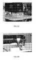
- FIGS. 7A and 7Ba circuit part 700 manufactured with the first two steps of the present invention is shown. More specifically, FIG. 7A is a photograph of the circuit part 700 , and FIG. 7B is an enlarged portion of circuit part 700 .
- the circuit part or three-dimensional electronic, electromagnetic or electromechanical component/device 700includes a substrate 702 with a plurality of interconnection cavities 704 and electronic component cavities 706 within the substrate.
- FIG. 8a component/device manufactured using the method in accordance with one embodiment of the present invention is shown.
- Thisis a substrate that was machined with a CNC router, interconnection channels filled with conductive media, and electronic components have been placed into their corresponding cavities.
- FIGS. 9A-9Dan example of an extrusion-based additive manufacturing system 900 for 3D structural electronic, electromagnetic or electromechanical components/devices in accordance with the present invention is shown. More specifically, FIGS. 9A-9B shows a partially completed system 900 , FIG. 9C shows a FDM tooling head, and FIG. 9D shows a DW microdispensing head.
- the system 900 for making a three-dimensional electronic, electromagnetic or electromechanical component/deviceincludes a fused deposition modeling machine 902 that creates one or more layers of a three-dimensional substrate by depositing a substrate material in a layer-by-layer fashion, a micro-machining machine or a laser ablation machine 904 that removes a portion of the substrate to form a plurality of interconnection cavities and electronic component cavities within the substrate, a direct-write or direct-print microdispensing machine 906 that fills the interconnection cavities with a conductive material, and a pick and place machine 908 that places one or more electronic components in the electronic component cavities.
- the laser 904can also cure the conductive material.
- the systemalso includes a pneumatic slide 910 that transports the three-dimensional substrate to each machine or sub-system. All of the machines can be integrated into a single machine or similar manufacturing system or process.
- parts produced by this inventionwill be used in various applications such as: 1) unmanned aerial systems (UASs) and unmanned aerial vehicles (UAVs) by providing aerodynamic parts with embedded sensors, communications and electronics within structural components or by directly fabricating onto UAS and UAV surfaces; 2) customized, mission-specific disposable electronics; 3) truly 3D antennas and photonic devices that improve communications; 4) replacement components for virtually any electronic system on a naval vessel; 5) custom fit sailor-borne electronics and communications systems; and 6) disposable floating depth-specific sensor systems; 7) biomedical devices; and 8) metamaterial structures.
- UASsunmanned aerial systems
- UAVsunmanned aerial vehicles
- the words “comprising” (and any form of comprising, such as “comprise” and “comprises”), “having” (and any form of having, such as “have” and “has”), “including” (and any form of including, such as “includes” and “include”) or “containing” (and any form of containing, such as “contains” and “contain”)are inclusive or open-ended and do not exclude additional, unrecited elements or method steps.
- A, B, C, or combinations thereofrefers to all permutations and combinations of the listed items preceding the term.
- “A, B, C, or combinations thereof”is intended to include at least one of: A, B, C, AB, AC, BC, or ABC, and if order is important in a particular context, also BA, CA, CB, CBA, BCA, ACB, BAC, or CAB.
- expressly includedare combinations that contain repeats of one or more item or term, such as BB, AAA, MB, BBC, AAABCCCC, CBBAAA, CABABB, and so forth.
- BBBB
- AAAAAA
- MBBBC
- AAABCCCCCCCBBAAA
- CABABBCABABB
- compositions and/or methods disclosed and claimed hereincan be made and executed without undue experimentation in light of the present disclosure. While the compositions and methods of this invention have been described in terms of preferred embodiments, it may be apparent to those of skill in the art that variations may be applied to the compositions and/or methods and in the steps or in the sequence of steps of the method described herein without departing from the concept, spirit and scope of the invention. All such similar substitutes and modifications apparent to those skilled in the art are deemed to be within the spirit, scope and concept of the invention as defined by the appended claims.
Landscapes
- Engineering & Computer Science (AREA)
- Manufacturing & Machinery (AREA)
- Chemical & Material Sciences (AREA)
- Materials Engineering (AREA)
- Microelectronics & Electronic Packaging (AREA)
- Physics & Mathematics (AREA)
- Mechanical Engineering (AREA)
- Power Engineering (AREA)
- Computer Hardware Design (AREA)
- Optics & Photonics (AREA)
- Composite Materials (AREA)
- Ceramic Engineering (AREA)
- Condensed Matter Physics & Semiconductors (AREA)
- General Physics & Mathematics (AREA)
- Micromachines (AREA)
Abstract
Description
- None.
- The present invention relates in general to the manufacture of electronic, electromagnetic and electromechanical components and devices, and more particularly to multiple material fabrication using an extrusion-based additive manufacturing system.
- None.
- None.
- Without limiting the scope of the invention, its background is described in connection with methods for manufacturing 3D objects and structures, more specifically 3D structural electronic, electromagnetic and electromechanical components and devices.
- U.S. Pat. No. 5,121,329 issued to Crump (1992) discloses an apparatus incorporating a movable dispensing head provided with a supply of material which solidifies at a predetermined temperature, and a base member, which are moved relative to each other along “X,” “Y,” and “Z” axes in a predetermined pattern to create three-dimensional objects by building up material discharged from the dispensing head onto the base member at a controlled rate. The apparatus is preferably computer driven in a process utilizing computer aided design (CAD) and computer-aided manufacturing (CAM) software to generate drive signals for controlled movement of the dispensing head and base member as material is being dispensed. Three-dimensional objects may be produced by depositing repeated layers of solidifying material until the shape is formed. Any material, such as self-hardening waxes, thermoplastic resins, molten metals, two-part epoxies, foaming plastics, and glass, which adheres to the previous layer with an adequate bond upon solidification, may be utilized and considered suitable for the process. Each layer base is defined by the previous layer, and each layer thickness is defined and closely controlled by the height at which the tip of the dispensing head is positioned above the preceding layer.
- The present invention describes an extrusion-based additive manufacturing system for 3D structural electronics that uses an innovative manufacturing process whereby multiple technologies are integrated into a single apparatus, device or machine to produce multi-material, heterogeneous, electronic structures exhibiting non-conventional component placement and sufficient mechanical properties.
- The present invention provides a method for making a three-dimensional electronic, electromagnetic or electromechanical component/device by: (1) creating one or more layers of a three-dimensional substrate by depositing a substrate material in a layer-by-layer fashion, wherein the substrate includes a plurality of interconnection cavities and component cavities; (2) filling the interconnection cavities with a conductive material; and (3) placing one or more electronic components in the component cavities. The process can be repeated to create additional layers of the three-dimensional substrate. The present invention also provides a three-dimensional electronic, electromagnetic or electromechanical component/device made by the foregoing method.
- In addition, the present invention provides a system for making a three-dimensional electronic, electromagnetic or electromechanical component/device that includes a three-dimensional printing device that creates one or more layers of a three-dimensional substrate by depositing a substrate material in a layer-by-layer fashion, wherein the substrate includes a plurality of interconnection cavities and component cavities. A first machine that fills the interconnection cavities with a conductive material. A component placement machine that places one or more components in the component cavities. The system may also include a slide, a conveyor or a robotic device that transports the three-dimensional substrate to each machine or sub-system.
- Moreover, the present invention provides a three-dimensional electronic, electromagnetic or electromechanical component/device made by a method comprising the steps of (a) creating one or more layers of a three-dimensional substrate by depositing a substrate material in a layer-by-layer fashion, wherein the substrate includes a plurality of interconnection cavities and component cavities, (b) filling the interconnection cavities with a conductive material, and (c) placing one or more components in the component cavities.
- For a more complete understanding of the features and advantages of the present invention, reference is now made to the detailed description of the invention along with the accompanying figures and in which:
FIG. 1 is a flow chart of a method for making a three-dimensional electronic, electromagnetic or electromechanical component/device in accordance with one embodiment of the present invention;FIG. 2 is a flow chart of a method for making a three-dimensional electronic, electromagnetic or electromechanical component/device in accordance with another embodiment of the present invention;FIG. 3 is a flow chart of method for making a three-dimensional electronic, electromagnetic or electromechanical component/device in accordance with another embodiment of the present invention;FIGS. 4A-4C show FDM-manufactured substrates with laser cut features demonstrating the feasibility of producing interconnection channels and component cavities with laser technologies in accordance with the present invention;FIGS. 5A-5C show a broadband anti-reflection grating andFIG. 5D shows a plot of the structure's performance in terms of electromagnetic reflectance, transmittance and conservation in accordance with various steps of the present invention;FIGS. 6A shows a CAD model for a scaled UAV wing andFIGS. 6B-6D show the scaled UAV wing fabricated with an FDM machine in accordance with various steps of the present invention;FIGS. 7A and 7B show a circuit part manufactured with the first two steps of the present invention;FIG. 8 shows a component/device manufactured using the method in accordance with one embodiment of the present invention; andFIGS. 9A-9D show an example of an extrusion-based additive manufacturing system for 3D structural electronic, electromagnetic and electromechanical components/devices in accordance with the present invention.- While the making and using of various embodiments of the present invention are discussed in detail below, it should be appreciated that the present invention provides many applicable inventive concepts that can be embodied in a wide variety of specific contexts. The specific embodiments discussed herein are merely illustrative of specific ways to make and use the invention and do not delimit the scope of the invention.
- To facilitate the understanding of this invention, a number of terms are defined below. Terms defined herein have meanings as commonly understood by a person of ordinary skill in the areas relevant to the present invention. Terms such as “a”, “an,” and “the” are not intended to refer to only a singular entity, but include the general class of which a specific example may be used for illustration. The terminology herein is used to describe specific embodiments of the invention, but their usage does not delimit the invention, except as outlined in the claims.
- One embodiment of the present invention provides an extrusion-based additive manufacturing system for 3D structural electronic, electromagnetic and electromechanical components/devices that utilizes fused deposition modeling (FDM), pick and place technology, computer numerical control (CNC) machining to develop an automated process that innovatively fabricates multi-material, heterogeneous, electronic, electromagnetic or electromechanical components/structures/devices without requiring assembly and exhibiting non-conventional component placement and sufficient mechanical properties and other material properties for the application. Some potentially relevant mechanical and material properties that may be required for the functional product may include impact resistance, elastic modulus, Poisson's ratio, flexural modulus and strength, tensile strength, creep, fatigue endurance, dielectric strength, dielectric constant, dissipation factor, thermal conductivity, deflection temperature, chemical resistivity, and water absorptivity. Additional processes can also be used as described below.
- Access to individual layers while a 3D object is additively fabricated as described in the present invention allows for the integration of other complementary technologies to produce multi-material and multi-functional structures and devices. Additive Manufacturing (AM) has been used in a hybrid stereolithography (SL) and direct write (DW) system that successfully fabricated a LM 555 circuit [5, 6, 8, 9].
- Fused deposition modeling (FDM) and direct-write, or direct print, technologies are used in the extrusion-based additive manufacturing system for fabricating 3D structural electronics, electromagnetic and electromechanical components/structures/devices. Electronic component placement in three-dimensions—different from the conventional planar placement in printed circuit board (PCB) arrangements—efficiently utilizes space and materials to satisfy mechanical and electrical design requirements of electronic, electromagnetic or electromechanical components/devices. Included in the new manufacturing process of the present invention is a subtractive manufacturing method (micro-machining) for the AM-fabricated substrate, which in the case of conventional FDM, is an extruded thermoplastic material. Tests conducted have proven the successful CNC micro-machining of interconnection channels as small as 230 μm. Laser ablation tests have also been performed and show greater resolutions which may not be possible with current CNC micro-machining Attributes of parts produced by this new invention are applicable in the electronics, electromechanical and biomedical industries.
- Although widely used, electronic components housed on conventional PCB arrangements are not able to withstand more than minimal physical loads. In addition, mechanical and electrical designs are often conflicted as both cannot be realized with the planar layout that PCBs provide. The present invention, extrusion-based additive manufacturing system for 3D structural electronic, electromagnetic and electromechanical components/devices, addresses both these issues as: 1) parts are fabricated in a layered fashion wherein electronic components can be placed anywhere within a complex 3D part thus resulting in the simultaneous fulfillment of mechanical and electrical design requirements; and 2) parts can be designed and fabricated to possess multi-functions, such as the capability to provide impact resistance and substantial structural support by including stress reducing features (e.g., arches, trusses, filets, etc.) as well as intelligence through the integrated electronics, electromagnetic structures (e.g., gratings, transmission lines, filters, etc.) or electromechanical structures (e.g., actuators, gauges, mechanical sensors, etc.). Moreover, component and interconnection cavities do not require chemical cleansing as in the case of stereolithography wherein solvents are used to remove uncured photopolymer. This cleaning process is described in [4, 5, 6, 7, 8, 9, 10]. Residual photopolymer and solvent are both detrimental to the quality and reliability of electronic circuits.
- One major drawback of a previously developed stereolithography/direct-write hybrid system with the capability of producing 3D electronic, electromagnetic and electromechanical components/devices is that the substrate material typically does not offer sufficient mechanical, thermal and electrical properties. Another limitation of prior systems is the 3D electronics are not impact resistant as parts tend to shatter when dropped. Moreover, the liquid resins used in stereolithography present problems during fabrication because the part and interconnection cavities have to be cleaned before components and conductive material can be embedded within the cavities. Further, once the components are inserted into the substrate and the conductive traces are added, the build may continue, causing the stereolithography liquid resin to possibly contaminate the inserted components and conductive traces, and require subsequent cleaning and removal of unreacted resin from the final part. These issues can negatively impact the reliability of the resulting components/devices. Conversely, the extrusion-based additive manufacturing system for 3D structural electronics uses a thermoplastic substrate to mitigate these deficiencies.
- Manufacture of 3D structural electronics has proven difficult with conventional manufacturing methods. Additive manufacturing provides the unique opportunity to access individual layers if process interruption is achieved. The present invention allows the fused deposition modeling (FDM) process to be interrupted so that electronic components or thermal management components can be embedded. FDM technology has not been used for structural electronics due to the lack of resolution required for electronic circuitry. It is expected that, as the use of additive processes for 3D electronics fabrication grows, the requirements for higher component and trace density will also grow. FDM is unable to compete with traditional PCB technologies in terms of trace density. Furthermore, many of the latest integrated circuits have geometries (e.g., pin pitch) that require a resolution greater than can be achieved with current FDM technology. The present invention solves the FDM resolution issue by employing subtractive manufacturing methods that are intermittently used during the additive manufacturing process to provide high resolution and accurate features. These subtractive manufacturing processes may include a micro-machining machine, a CNC micro-machining machine, a micro electrical discharge machining machine, an electrochemical machining machine, a direct write proton micro-machining machine, a laser ablation machine, a radiative source, an ultrasonic cutting machine, a hot wire cutting machine, a waterjet machine, an etching machine, a deep reactive ion etching machine, a plasma etching machine, a crystal orientation dependent etching machine, a wet bulk micromachining machine, a UV-lithography or X-ray lithography (LIGA) machine, a hot embossing lithography machine, a precision mechanical sawing machine, a chemically assisted ion milling machine, a sand blasting machine, a cutting machine, or other suitable systems. CNC micromachining can achieve interconnection channels as small as 230 μm while laser micro-machining can be used to produce relatively smaller features.
- The extrusion-based additive manufacturing system for 3D structural electronics addresses the limitations of the planar arrangement in a conventional PCB. Non-conventional placement of electronic components in a complex 3D part will enable the evolution of circuitry design. That is, parts will be limited by designs rather than manufacturing capabilities as is the current state-of-the-art. PCBs use a substrate that provides mechanical stability for component interconnections and require a housing to provide structural support for the entire electronic, electromagnetic or electromechanical component/device. The present invention provides components/devices with structural support without having to use a housing unless such a housing is desired.
- The extrusion-based additive manufacturing system for 3D structural electronics has applications in the electronics industry as it promises to dramatically reduce manufacturing cost by, for example, eliminating the requirement of always having a housing to provide structural support. Government agencies, such as the Department of Defense, can use the present invention in a wide variety of applications including, but not limited to: 1) unmanned aerial systems (UASs) or unmanned aerial vehicles (UAVs) by providing aerodynamic parts with embedded sensors, communications and electronics within structural components or by directly fabricating onto UAS and UAV surfaces; 2) customized, mission-specific disposable electronics; 3) truly 3D antennas and photonic devices that improve communications; 4) replacement components for virtually any electronic system on a naval vessel; 5) custom fit sailor-borne electronics and communications systems; and 6) disposable floating depth-specific sensor systems. The invention can also be used in structural health monitoring, where 3D electronics are expected to play an important role in the future. This invention will allow real-time nondestructive monitoring of structural parts where sensors can be strategically placed in a complex part, which is very difficult to do with current manufacturing processes.
- Now referring to
FIG. 1 , a flow chart of amethod 100 for making a three-dimensional electronic, electromagnetic or electromechanical component/device in accordance with one embodiment of the present invention is shown. One or more layers of a three-dimensional substrate is/are created by depositing a substrate material in a layer-by-layer fashion inblock 102. The substrate material may include a thermoplastic material as is typically used in FDM, or alternatively may include another polymer material, a ceramic material, a metallic material, a mineral material, a glass ceramic material, a semi-conductor material, a nanomaterial, a biomaterial, an organic material, an inorganic material, or any combination thereof. The substrate includes a plurality of interconnection cavities and component cavities. The thermoplastic material can be a material currently used commercially in FDM, such as acrylonitrile butadiene styrene (ABS), ABSi, ABSplus, ABS-M30, ABS-M30i, polycarbonate (PC), PC-ABS, PC-ISO, polyphenylsulfone (PPSF/PPSU), ULTEM 9085, or other material available from the FDM manufacturer; or alternatively, virtually any extrudable material such as poly(methyl methacrylate) (PMMA), polypropylene, polyolefin, LL-PE, HDPE, polyvinyl acetate, polyester, polyamides, nylon, polyimides, polyketone, polyether ethyl ketone (PEEK), polybutadiene, polylactic acid, polycaprolactone, polyethylene terephthalate, liquid crystalline polymer (LCP), polystyrene, polyvinyl chloride, polyfluoroethylene, polydifluoroethylene, polytetrafluoroethylene, ZEONEX RS420, Eccostock HIK-TPO, co-polymers and block co-polymers of the previous, or any other suitable material and any combination thereof. Moreover, the one or more layers can be deposited using a three-dimensional printing process, a fused deposition modeling process or other suitable process. The interconnection cavities may include an interconnection channel, a pin cavity and/or a via. The portion of the substrate can be removed using a micro-machining process, a laser ablation process or other suitable process. The interconnection cavities are filled with a conductive material inblock 104. The conductive material can be a metal, a metal alloy, an ink containing conductive particles (e.g., silver particles), a conductive polymer, a wire or other suitable material. Note that filling the interconnections cavities can be done by inserting, placing or otherwise causing the conductive material (e.g., a liquid, a paste, a wire-bond, a filament, a solid, etc.) to be within the interconnection cavity. The interconnection cavities can be filled using a direct-write microdispensing process, a direct-print microdispensing process, a fused deposition modeling head, another extrusion-based deposition system, an inkjet dispensing system, a spray machine, a wire bonding machine, a solder machine, a photolithographic technique, an electrodeposition machine, a damascene process, a rotogravure machine, an electro sputtering machine or other suitable process. Additionally, the interconnection cavities may be filled by physically embedding electrical conductors. Subsequently, an ultrasonic staking machine may be used to secure the electrical conductor or components. - One or more components are placed (automatically, semi-automatically, manually, etc.) in the component cavities in
block 106. The electronic components may include an electronic component (e.g., an integrated circuit, a resistor, a capacitor, an inductor, a transistor, a thermistor, a thyristor, a sensor, a processor, a memory, an interface device, a display, a power source, an energy conversion device or an antenna), an electrostatic component, a pneumatic component, an electroacoustic component, a microelectromechanical system (MEMS), a biomedical component, an electrochemical component, an electromechanical component, an electromagnetic component, a mechanical component, a metamaterial component, an optical component, a photonic component, a thermal component, a thermal management component, or any other desired component. The electronic components can be placed by hand or by using a component placement machine, such as a pick and place machine, a robotic process or other automated component placement technology. In some embodiments, the conductive material is cured. The conductive material can be cured using a laser, an Ohmic curing process, an inductive curing process, a radiation curing process, a thermal curing process, an electric polarization process or a magnetic polarization process or other suitable process. Several of these methods of curing are described in [8, 9, 10, 11] as examples. Moreover, the curing can be localized or directed to a specific conductive material rather than exposing the entire structure to the extremes necessary for the curing. Localized, high energy fluxes will also ensure an energy efficient process. Note that the curing step can be eliminated whenever a self-curing conductive material is used. As indicated byline 108, the process (blocks - The plurality of interconnection cavities and component cavities within the substrate can be created by removing a portion of the substrate using a micro-machining machine, a CNC micro-machining machine, a micro electrical discharge machining machine, an electrochemical machining machine, a direct write proton micro-machining machine, a laser ablation machine, a radiative source, an ultrasonic cutting machine, a hot wire cutting machine, a waterjet machine, an etching machine, a deep reactive ion etching machine, a plasma etching machine, a crystal orientation dependent etching machine, a wet bulk micromachining machine, a UV-lithography or X-ray lithography (LIGA) machine, a hot embossing lithography machine, a precision mechanical sawing machine, a chemically assisted ion milling machine, a sand blasting machine, a cutting machine, or other suitable systems. As an example,
FIGS. 4A-4C show FDM-manufactured substrates with laser cut features demonstrating the feasibility of producing interconnection channels and component cavities with laser technologies. In addition, a portion of the substrate can be removed for a diffraction grating, an electromagnetically responsive structure, a cooling channel, a vent or any other desired structure. As an example,FIGS. 5A-5C show a broadband anti-reflection grating andFIG. 5D shows a plot of the structure's performance in terms of electromagnetic reflectance, transmittance and conservation. Moreover, the process may also include the step of depositing a thermally conductive material, a ceramic material, a dielectric material, a magnetic material, a piezoelectric material, an insulating material, an elastomer, a wax, a resin, an epoxy, a plastic material, a glass or any combination thereof on the substrate. The three-dimensional substrate can be transported to the various machines using a slide, a conveyor, a robotic device or other suitable transport mechanism. - In another embodiment, cavities are not formed in the substrate. Instead, the components and/or conductive materials are deposited or inserted directly on a layer of the substrate material. One or more additional layers of substrate material are then deposited on top of the components and/or conductive materials. As an example,
FIGS. 6A shows a CAD model for a scaled UAV wing andFIGS. 6B-6D show the scaled UAV wing fabricated with an FDM machine. Cavities for several discrete components such as capacitors, resistors, inductors, and interconnection pins were designed with SolidWorks. As in [12], embedded electronic components were inserted into their respective cavities; however, the conductive inks were printed directly on the conformal substrate without the need for interconnection cavities. - Referring now to
FIG. 2 , a flow chart ofmethod 200 for making a three-dimensional electronic, electromagnetic or electromechanical component/device in accordance with another embodiment of the present invention is shown. The process starts inblock 202. If high resolution features are required, as determined indecision block 204, the substrate material is deposited using FDM inblock 206, substrate material is selectively removed to produce high resolution features inblock 208, and the electronic component cavities are populated and the interconnection channels are filled inblock 210. If, however, high resolution features are not required, as determined indecision block 204, the electronic substrate including low resolution features is fabricated using FDM inblock 212, and the electronic component cavities are populated and the interconnection channels are filled inblock 210. If post-processing is required for conductive media, as determined indecision block 214, the conductive media is post-processed inblock 216. Thereafter or if post-processing is not required for conductive media, as determined indecision block 214, the process repeats by looping back to decision block204 whenever additional layers with embedded electronics are required, as determined indecision block 218. If, however, additional layers are not required, as determined indecision block 218, the process ends inblock 220. - Now referring to
FIG. 3 , a flow chart ofmethod 300 for making a three-dimensional electronic, electromagnetic or electromechanical component/device in accordance with another embodiment of the present invention is shown. TheFDM phase 302 includes the step of depositing a substrate material (e.g., a thermoplastic material) in a layer-by-layer fashion to function as: 1) a substrate for conductive media; and 2) structural support for the device. Materials development studies have been conducted to adopt new thermoplastics (e.g., PMMA [13], polycaprolactone [14], polypropylene, ZEONEX RS420, Eccostock HIK-TPO) for theFDM process 302 that will enable the fabrication of devices whose attributes find applications in the electronic and biomedical industries. Some of these materials exhibit improved properties relevant to the application. As an example of a biomedical material, PMMA is used as a bone cement due to its relatively high tensile strength (60 MPa) and high softening temperature (125° C.). ZEONEX RS420 is an example of a substrate material for use in the electronic industry due to its low dielectric tangent loss (0.0002 at 1 MHz) and dielectric constant (2.3 at 1 MHz). After a specified number of layers have been deposited, a pneumatic stage312 (or other transport mechanism) will transport the workpiece to themicro-machining phase 304. Between all phases, thepneumatic slide 312 is used to transport the work piece. The feature resolution achieved by FDM is not sufficient for electronic circuitry and therefore micro-machining304—either by laser, CNC or other suitable process—is required. In themicromachining phase 304, the substrate is machined to produce features (e.g.,FIGS. 7A and 7B ) that include interconnection channels, component cavities, and vias or serve as a finishing process to achieve the required resolution and accuracy. Once machined, the workpiece is delivered to theDW phase 306 where conductive media (e.g., silver ink or other suitable material) is dispensed into the interconnection channels and pin locations. Electronic components (e.g., microprocessors, capacitors, resistors, etc.) are placed in their respective cavities by hand or by utilizing pick andplace technology 308 or other similar automated component placement technology. One manufacturing cycle is completed with the processing of the conductive media. That is, the silver ink is cured with the use of alaser 310 or other suitable process. In addition, the silver particles within the ink are sintered by using laser energy. Themanufacturing process 300 is repeated until a complete part, with embedded components, is produced. Note that machines may not be required to perform every portion of themanufacturing process 300. - Note that the previously described methods can be implemented using a computer program embodied on a non-transitory computer readable medium wherein the steps are performed using one or more code segments.
- Referring now to
FIGS. 7A and 7B , acircuit part 700 manufactured with the first two steps of the present invention is shown. More specifically,FIG. 7A is a photograph of thecircuit part 700, andFIG. 7B is an enlarged portion ofcircuit part 700. The circuit part or three-dimensional electronic, electromagnetic or electromechanical component/device 700 includes asubstrate 702 with a plurality ofinterconnection cavities 704 andelectronic component cavities 706 within the substrate. - Now referring to
FIG. 8 , a component/device manufactured using the method in accordance with one embodiment of the present invention is shown. This is a substrate that was machined with a CNC router, interconnection channels filled with conductive media, and electronic components have been placed into their corresponding cavities. - Referring now to
FIGS. 9A-9D , an example of an extrusion-basedadditive manufacturing system 900 for 3D structural electronic, electromagnetic or electromechanical components/devices in accordance with the present invention is shown. More specifically,FIGS. 9A-9B shows a partially completedsystem 900,FIG. 9C shows a FDM tooling head, andFIG. 9D shows a DW microdispensing head. Thesystem 900 for making a three-dimensional electronic, electromagnetic or electromechanical component/device includes a fuseddeposition modeling machine 902 that creates one or more layers of a three-dimensional substrate by depositing a substrate material in a layer-by-layer fashion, a micro-machining machine or alaser ablation machine 904 that removes a portion of the substrate to form a plurality of interconnection cavities and electronic component cavities within the substrate, a direct-write or direct-print microdispensing machine 906 that fills the interconnection cavities with a conductive material, and a pick andplace machine 908 that places one or more electronic components in the electronic component cavities. Thelaser 904 can also cure the conductive material. The system also includes apneumatic slide 910 that transports the three-dimensional substrate to each machine or sub-system. All of the machines can be integrated into a single machine or similar manufacturing system or process. - As previously mentioned, parts produced by this invention will be used in various applications such as: 1) unmanned aerial systems (UASs) and unmanned aerial vehicles (UAVs) by providing aerodynamic parts with embedded sensors, communications and electronics within structural components or by directly fabricating onto UAS and UAV surfaces; 2) customized, mission-specific disposable electronics; 3) truly 3D antennas and photonic devices that improve communications; 4) replacement components for virtually any electronic system on a naval vessel; 5) custom fit sailor-borne electronics and communications systems; and 6) disposable floating depth-specific sensor systems; 7) biomedical devices; and 8) metamaterial structures.
- It may be understood that particular embodiments described herein are shown by way of illustration and not as limitations of the invention. The principal features of this invention can be employed in various embodiments without departing from the scope of the invention. Those skilled in the art will recognize, or be able to ascertain using no more than routine experimentation, numerous equivalents to the specific procedures described herein. Such equivalents are considered to be within the scope of this invention and are covered by the claims.
- All publications, patents and patent applications mentioned in the specification are indicative of the level of skill of those skilled in the art to which this invention pertains. All publications, patents and patent applications are herein incorporated by reference to the same extent as if each individual publication, patent or patent application was specifically and individually indicated to be incorporated by reference.
- The use of the word “a” or “an” when used in conjunction with the term “comprising” in the claims and/or the specification may mean “one,” but it is also consistent with the meaning of “one or more,” “at least one,” and “one or more than one.” The use of the term “or” in the claims is used to mean “and/or” unless explicitly indicated to refer to alternatives only or the alternatives are mutually exclusive, although the disclosure supports a definition that refers to only alternatives and “and/or.” Throughout this application, the term “about” is used to indicate that a value includes the inherent variation of error for the device, the method being employed to determine the value, or the variation that exists among the study subjects.
- As used in this specification and claim(s), the words “comprising” (and any form of comprising, such as “comprise” and “comprises”), “having” (and any form of having, such as “have” and “has”), “including” (and any form of including, such as “includes” and “include”) or “containing” (and any form of containing, such as “contains” and “contain”) are inclusive or open-ended and do not exclude additional, unrecited elements or method steps.
- The term “or combinations thereof” as used herein refers to all permutations and combinations of the listed items preceding the term. For example, “A, B, C, or combinations thereof” is intended to include at least one of: A, B, C, AB, AC, BC, or ABC, and if order is important in a particular context, also BA, CA, CB, CBA, BCA, ACB, BAC, or CAB. Continuing with this example, expressly included are combinations that contain repeats of one or more item or term, such as BB, AAA, MB, BBC, AAABCCCC, CBBAAA, CABABB, and so forth. The skilled artisan will understand that typically there is no limit on the number of items or terms in any combination, unless otherwise apparent from the context.
- All of the compositions and/or methods disclosed and claimed herein can be made and executed without undue experimentation in light of the present disclosure. While the compositions and methods of this invention have been described in terms of preferred embodiments, it may be apparent to those of skill in the art that variations may be applied to the compositions and/or methods and in the steps or in the sequence of steps of the method described herein without departing from the concept, spirit and scope of the invention. All such similar substitutes and modifications apparent to those skilled in the art are deemed to be within the spirit, scope and concept of the invention as defined by the appended claims.
- 1. U.S. Pat. No. 5,121,329: Apparatus and Method for Creating Three-Dimensional Objects.
- 2. U.S. Patent Application Publication No. 2011/0121476: Encoded Consumable Materials and Sensor Assemblies for Use in Additive Manufacturing Systems.
- 3. U.S. Pat. No. 7,555,357: Method for Building Three-Dimensional Objects with Extrusion-Based Layered Deposition Systems.
- 4. U.S. Pat. No. 7,556,490: Multi-Material Stereolithography.
- 5. U.S. Pat. No. 7,419,630: Methods and Systems for Rapid Prototyping of High Density Circuits.
- 6. U.S. Pat. No. 7,658,603: Methods and System for Integrating Fluid Dispensing Technology with Stereolithography.
- 7. U.S. Pat. No. 7,959,847: Methods for Multi-Material Stereolithography.
- 8. Lopes, A. J., MacDonald, E., Wicker, R., Integrating stereolithography and direct print technologies for 3D structural electronics fabrication. Rapid Prototyping Journal, Volume 18, Issue 2, 2012.
- 9. Lopes, A., Navarrete, M., Medina, F., Palmer, J., MacDonald, E., Wicker, R., (2006). Expanding rapid prototyping for electronic systems integration of arbitrary form. 17th Annual Solid Freeform Fabrication Symposium, University of Texas at Austin, August 14-16.
- 10. Amit Joe Lopes, “Hybrid manufacturing: Integrating stereolithography and direct print technologies,” Ph.D. Dissertation, The University of Texas at El Paso, 2010, 128 pages.
- 11. D. A. Roberson, R. B. Wicker, L. E. Murr, K. Church, and E. MacDonald, “Microstructural and Process Characterization of Conductive Traces Printed from Ag Particulate Inks,” Materials, Volume 4, Issue 6, 2011, pages 963-979.
- 12. Olivas, R., Salas, R., Muse, D., MacDonald, E., Wicker, R. Structural electronics through additive manufacturing and micro-dispensing. IMAPS National Conference, October 2010.
- 13. Espalin, D., Arcaute, K., Rodriguez, D., Medina, F., Posner, M., Wicker, R. Fused deposition modeling of patient-specific polymethylmethacrylate implants. Rapid Prototyping Journal,
Volume 16, Issue 3, 2010. - 14. Zein. I., Hutmacher, D. W., Tan, K. C., Teoh, S. H. Fused deposition modeling of novel scaffold architectures for tissue engineering applications. Biomaterials, Volume 23, Issue 4, 2002.
Claims (70)
Priority Applications (4)
| Application Number | Priority Date | Filing Date | Title |
|---|---|---|---|
| US13/343,651US10748867B2 (en) | 2012-01-04 | 2012-01-04 | Extrusion-based additive manufacturing system for 3D structural electronic, electromagnetic and electromechanical components/devices |
| PCT/US2012/072100WO2013103600A1 (en) | 2012-01-04 | 2012-12-28 | Extrusion-based additive manufacturing system for 3d structural electronic, electromagnetic and electromechanical components/devices |
| US13/829,921US9414501B2 (en) | 2012-01-04 | 2013-03-14 | Method for connecting inter-layer conductors and components in 3D structures |
| US15/185,078US10660214B2 (en) | 2012-01-04 | 2016-06-17 | Methods for connecting inter-layer conductors and components in 3D structures |
Applications Claiming Priority (1)
| Application Number | Priority Date | Filing Date | Title |
|---|---|---|---|
| US13/343,651US10748867B2 (en) | 2012-01-04 | 2012-01-04 | Extrusion-based additive manufacturing system for 3D structural electronic, electromagnetic and electromechanical components/devices |
Publications (2)
| Publication Number | Publication Date |
|---|---|
| US20130170171A1true US20130170171A1 (en) | 2013-07-04 |
| US10748867B2 US10748867B2 (en) | 2020-08-18 |
Family
ID=48694648
Family Applications (1)
| Application Number | Title | Priority Date | Filing Date |
|---|---|---|---|
| US13/343,651Active2033-07-16US10748867B2 (en) | 2012-01-04 | 2012-01-04 | Extrusion-based additive manufacturing system for 3D structural electronic, electromagnetic and electromechanical components/devices |
Country Status (2)
| Country | Link |
|---|---|
| US (1) | US10748867B2 (en) |
| WO (1) | WO2013103600A1 (en) |
Cited By (91)
| Publication number | Priority date | Publication date | Assignee | Title |
|---|---|---|---|---|
| US20130297062A1 (en)* | 2012-05-03 | 2013-11-07 | Alberto Daniel Lacaze | Field Deployable Rapid Prototypable UXVs |
| CN103665905A (en)* | 2013-12-18 | 2014-03-26 | 广州市傲趣电子科技有限公司 | 3D (three dimensional) wood printing supply and preparation method thereof |
| CN103937278A (en)* | 2014-05-13 | 2014-07-23 | 江苏锦禾高新科技股份有限公司 | 3D printing wood-plastic composite material and preparation method thereof |
| US20140268604A1 (en)* | 2013-03-14 | 2014-09-18 | Board Of Regents, The University Of Texas System | Methods and Systems For Embedding Filaments in 3D Structures, Structural Components, and Structural Electronic, Electromagnetic and Electromechanical Components/Devices |
| CN104194334A (en)* | 2014-07-29 | 2014-12-10 | 中国科学院重庆绿色智能技术研究院 | Plastic consumable for fused deposition technology and preparation method thereof |
| US20150001762A1 (en)* | 2013-06-27 | 2015-01-01 | Alberto Daniel Lacaze | Method for Deployable Rapid On-Site Manufacturing Using 3D Printing in Combination with Vacuum Metallization |
| WO2015110293A1 (en)* | 2014-01-22 | 2015-07-30 | Robert Bosch Gmbh | Electronic functional component and method for producing an electronic functional component |
| WO2015148521A1 (en)* | 2014-03-26 | 2015-10-01 | Purdue Research Foundation | Composition and filament for 3d printer |
| EP2927016A1 (en)* | 2014-04-04 | 2015-10-07 | Flooring Technologies Ltd. | Method for manufacturing a decorative panel and decorative panel |
| WO2015153400A1 (en)* | 2014-03-30 | 2015-10-08 | Stanley Korn | System, method and apparatus for 3d printing |
| WO2015150548A1 (en)* | 2014-04-04 | 2015-10-08 | Feinmetall Gmbh | Contact-distance transformer, electrical testing device, and method for producing a contact-distance transformer |
| WO2016018297A1 (en)* | 2014-07-30 | 2016-02-04 | Hewlett-Packard Development Company, L. P. | Detecting vascular conditions in animal bodies |
| US20160046385A1 (en)* | 2014-08-18 | 2016-02-18 | The Boeing Company | Methods and apparatus for use in forming a lightning protection system |
| WO2016036854A1 (en)* | 2014-09-02 | 2016-03-10 | The Board Of Trustees Of The Leland Stanford Junior University | Passive components for electronic circuits using conformal deposition on a scaffold |
| US20160147217A1 (en)* | 2014-11-25 | 2016-05-26 | Autodesk, Inc. | Techniques for generating materials to satisfy design criteria |
| CN105682724A (en)* | 2013-08-29 | 2016-06-15 | 富特姆4有限公司 | Electronic smoking device configured for automated assembly |
| US9414501B2 (en) | 2012-01-04 | 2016-08-09 | Board Of Regents, The University Of Texas System | Method for connecting inter-layer conductors and components in 3D structures |
| WO2016146374A1 (en)* | 2015-03-17 | 2016-09-22 | Philips Lighting Holding B.V. | Making 3d printed shapes with interconnects and embedded components. |
| WO2016149181A1 (en)* | 2015-03-19 | 2016-09-22 | Board Of Regents, The University Of Texas System | Structurally integrating metal objects into additive manufactured structures |
| FR3033977A1 (en)* | 2015-03-20 | 2016-09-23 | Thales Sa | METHOD FOR MANUFACTURING A PRINTED CIRCUIT AND CORRESPONDING PRINTED CIRCUITS |
| WO2016171840A1 (en)* | 2015-04-21 | 2016-10-27 | Northrop Grumman Systems Corporation | High performance, ultra low loss, ultra lightweight, multi-layered rigid circuit boards |
| US20160325487A1 (en)* | 2014-02-24 | 2016-11-10 | Empire Technology Development Llc | Increased interlayer adhesion of three-dimensional printed articles |
| GB2538522A (en)* | 2015-05-19 | 2016-11-23 | Dst Innovations Ltd | Electronic circuit and component construction |
| US9559038B2 (en) | 2015-04-30 | 2017-01-31 | Deere & Company | Package for a semiconductor device |
| US9564385B2 (en) | 2015-04-30 | 2017-02-07 | Deere & Company | Package for a semiconductor device |
| WO2017045421A1 (en)* | 2015-09-17 | 2017-03-23 | 中芯长电半导体(江阴)有限公司 | Chip packaging method |
| EP3151641A1 (en)* | 2015-09-30 | 2017-04-05 | Siemens Aktiengesellschaft | Method and device for wiring a technical system and technical system |
| US9643282B2 (en) | 2014-10-17 | 2017-05-09 | Kennametal Inc. | Micro end mill and method of manufacturing same |
| WO2017102065A1 (en)* | 2015-12-18 | 2017-06-22 | Liebherr-Components Biberach Gmbh | Switchboard comprising a base plate for a switchgear cabinet, and method for manufacturing same in a 3d printing process |
| EP3202573A1 (en)* | 2016-02-04 | 2017-08-09 | Sick AG | Optoelectronic sensor and method of producing same |
| US20170225273A1 (en)* | 2016-02-08 | 2017-08-10 | Board Of Regents, The University Of Texas System | Connecting metal foils/wires and components in 3d printed substrates with wire bonding |
| US20170254065A1 (en)* | 2016-03-07 | 2017-09-07 | Airbus Operations Gmbh | Lining Panel With Integrated Electric Lines For An Aircraft And Method For Manufacturing A Lining Panel |
| WO2017155683A1 (en)* | 2016-03-09 | 2017-09-14 | Commscope Technologies Llc | 3-d printing process for forming flat panel array antenna |
| US20170274974A1 (en)* | 2016-03-24 | 2017-09-28 | Airbus Operations Gmbh | Method for manufacturing a lining panel with an integrated electrical connector for an aircraft or spacecraft, lining panel and lining panel assembly |
| EP3282527A1 (en)* | 2016-08-08 | 2018-02-14 | Siemens Aktiengesellschaft | Air conditioning of electrical devices by means of compressed air |
| US20180043618A1 (en)* | 2015-03-02 | 2018-02-15 | The Board Of Regents, The University Of Texas System | Embedding apparatus and method utilizing additive manufacturing |
| US9910935B2 (en)* | 2013-10-11 | 2018-03-06 | Advanced Solutions Life Sciences, Llc | System and workstation for the design, fabrication and assembly of bio-material constructs |
| US9908037B2 (en) | 2013-07-11 | 2018-03-06 | Board Of Regents, The University Of Texas System | Electronic gaming die |
| US9966180B2 (en) | 2016-01-22 | 2018-05-08 | Raytheon Company | Impedance transformer |
| WO2018091193A1 (en)* | 2016-11-16 | 2018-05-24 | Robert Bosch Gmbh | 3-d printing method having increased strength of the produced object |
| WO2018136567A1 (en)* | 2017-01-17 | 2018-07-26 | Terry Daglow | Apparatus and device to function as an electrical lead consisting of electrodes for neurological stimulation and signal recording |
| US10058890B1 (en)* | 2015-11-20 | 2018-08-28 | Seagate Technology Llc | Methods of forming an air bearing surface on a slider and related sliders |
| WO2018157210A1 (en) | 2017-03-02 | 2018-09-07 | Saluda Medical Pty Limited | Printed lead |
| US20180265417A1 (en)* | 2015-01-23 | 2018-09-20 | Hewlett-Packard Development Company, L.P. | Susceptor materials for 3d printing using microwave processing |
| US20180302989A1 (en)* | 2013-09-27 | 2018-10-18 | Tactotek Oy | Apparatus for carrying out a manufacturing method on an electro chemical structure |
| US10105769B2 (en) | 2014-04-17 | 2018-10-23 | Kennametal Inc. | Machining tool and method for manufacturing a machining tool |
| WO2019008444A1 (en)* | 2017-07-05 | 2019-01-10 | Coats Group Plc | Fiber preform of commingled fiber bundle for overmolding |
| US10222785B2 (en)* | 2014-09-26 | 2019-03-05 | Endress-Hauser SE+Co. KG | Method for manufacturing a component of a field device |
| US10232443B2 (en) | 2015-12-16 | 2019-03-19 | Desktop Metal, Inc. | Fused filament fabrication |
| US10369636B2 (en) | 2014-04-17 | 2019-08-06 | Kennametal Inc. | Machining tool and method for manufacturing a machining tool |
| CN110093021A (en)* | 2019-05-22 | 2019-08-06 | 吉林大学 | A polylactic acid modified shape memory intelligent deformation material and its preparation method |
| US10427353B2 (en)* | 2016-05-13 | 2019-10-01 | Ricoh Company, Ltd. | Additive manufacturing using stimuli-responsive high-performance polymers |
| US20190300741A1 (en)* | 2018-04-03 | 2019-10-03 | Massachusetts Institute Of Technology | 3-d printed devices formed with conductive inks and method of making |
| US10464306B2 (en) | 2015-04-17 | 2019-11-05 | Board Of Regents, The University Of Texas System | Metal objects spanning internal cavities in structures fabricated by additive manufacturing |
| EP3578346A1 (en)* | 2014-07-18 | 2019-12-11 | HARTING Electric GmbH & Co. KG | Method for data provision |
| US10569464B2 (en) | 2016-02-08 | 2020-02-25 | Board Of Regents, The University Of Texas System | Connecting metal foils/wires at different layers in 3D printed substrates with wire spanning |
| US10582619B2 (en) | 2015-08-24 | 2020-03-03 | Board Of Regents, The University Of Texas System | Apparatus for wire handling and embedding on and within 3D printed parts |
| US10595440B2 (en) | 2018-03-02 | 2020-03-17 | Northrop Grumman Systems Corporation | Thermal gasket with high transverse thermal conductivity |
| CN111032317A (en)* | 2017-08-11 | 2020-04-17 | 昕诺飞控股有限公司 | Method for manufacturing 3D object with conductive coil |
| EP3352971B1 (en) | 2015-09-24 | 2020-04-22 | Victrex Manufacturing Limited | Polymeric materials |
| US10667403B2 (en)* | 2014-09-19 | 2020-05-26 | Fuji Corporation | Manufacturing apparatus for performing additive manufacturing of an electrical device |
| US10665581B1 (en) | 2019-01-23 | 2020-05-26 | Sandisk Technologies Llc | Three-dimensional semiconductor chip containing memory die bonded to both sides of a support die and methods of making the same |
| US10683381B2 (en) | 2014-12-23 | 2020-06-16 | Bridgestone Americas Tire Operations, Llc | Actinic radiation curable polymeric mixtures, cured polymeric mixtures and related processes |
| US10748867B2 (en)* | 2012-01-04 | 2020-08-18 | Board Of Regents, The University Of Texas System | Extrusion-based additive manufacturing system for 3D structural electronic, electromagnetic and electromechanical components/devices |
| US10828852B1 (en) | 2019-08-20 | 2020-11-10 | Honeywell International Inc. | Embedding electronics in housing using additive manufacturing |
| US10881037B2 (en) | 2016-12-28 | 2020-12-29 | Microsoft Technology Licensing, Llc | Metal additive structures on printed circuit boards |
| US10879260B2 (en) | 2019-02-28 | 2020-12-29 | Sandisk Technologies Llc | Bonded assembly of a support die and plural memory dies containing laterally shifted vertical interconnections and methods for making the same |
| CN112549523A (en)* | 2020-11-16 | 2021-03-26 | 华中科技大学 | Material increasing and decreasing integrated molding system and method for three-dimensional conformal electronic component |
| US11009867B1 (en)* | 2017-07-28 | 2021-05-18 | Rockwell Collins, Inc. | Low-cost distributed multifunction radio frequency (MFRF) swarming unmanned aircraft systems (UAS) |
| US11037706B2 (en)* | 2018-05-15 | 2021-06-15 | Aptiv Technologies Limited | Apparatus and method for manufacturing assembly having multiple separated conductors embedded within a substrate |
| US11097531B2 (en) | 2015-12-17 | 2021-08-24 | Bridgestone Americas Tire Operations, Llc | Additive manufacturing cartridges and processes for producing cured polymeric products by additive manufacturing |
| US20210362411A1 (en)* | 2018-03-13 | 2021-11-25 | Hewlett-Packard Development Company, L.P. | Fusing electronic components into three-dimensional objects via additive manufacturing processes |
| US11260556B2 (en)* | 2016-07-20 | 2022-03-01 | Hewlett-Packard Development Company, L.P. | Additive manufacturing in an atmosphere including oxygen |
| US11292622B2 (en)* | 2013-10-07 | 2022-04-05 | Shay C. Colson | 3D printed vehicle packaging |
| WO2022081262A1 (en)* | 2020-10-14 | 2022-04-21 | Applied Materials, Inc. | Hybrid printing platform for 3d bioprinting of live organs |
| US11317515B2 (en) | 2016-09-06 | 2022-04-26 | Board Of Regents, The University Of Texas System | Wire embedding system with a curved delivery path |
| US11406020B2 (en)* | 2016-09-26 | 2022-08-02 | Imec Vzw | Method of manufacturing a flat device |
| WO2022177571A1 (en)* | 2021-02-19 | 2022-08-25 | Hewlett-Packard Development Company, L.P. | Plastically deformable 3d objects with heat channels |
| US11453161B2 (en) | 2016-10-27 | 2022-09-27 | Bridgestone Americas Tire Operations, Llc | Processes for producing cured polymeric products by additive manufacturing |
| US11465354B2 (en)* | 2020-01-06 | 2022-10-11 | The Boeing Company | Fabrication of additive manufacturing parts |
| US20230012318A1 (en)* | 2021-07-09 | 2023-01-12 | Toyota Motor Engineering & Manufacturing North America, Inc. | Systems and methods of 3d-printing a circuit board on a heat sink assembly having power devices bonded thereto |
| WO2023016720A1 (en)* | 2021-08-10 | 2023-02-16 | Robert Bosch Gmbh | Hybrid manufacture of three-dimensional components |
| CN115946339A (en)* | 2022-12-28 | 2023-04-11 | 中国科学院福建物质结构研究所 | A preparation method of high-conductivity FDM 3D printing parts |
| US11648731B2 (en) | 2015-10-29 | 2023-05-16 | Hewlett-Packard Development Company, L.P. | Forming three-dimensional (3D) printed electronics |
| US11699942B2 (en) | 2019-05-23 | 2023-07-11 | GM Global Technology Operations LLC | Hybrid additive manufacturing assisted prototyping for making electro-mechanical components |
| US11834206B1 (en)* | 2017-04-13 | 2023-12-05 | Redwire Space, Inc. | Universal long-term in space structural erection system |
| US11845219B2 (en) | 2019-05-06 | 2023-12-19 | Massachusetts Institute Of Technology | 3-d printed devices formed with magnetic inks and methods of making graded index structures |
| US11887766B2 (en) | 2020-08-24 | 2024-01-30 | Ge Aviation Systems Llc | Magnetic component and method of forming |
| US20240146395A1 (en)* | 2022-10-31 | 2024-05-02 | At&T Intellectual Property I, L.P. | Using unmanned mobile vehicles to improve signal propagation by placing temporary access points |
| US11984711B2 (en) | 2018-03-23 | 2024-05-14 | Hitachi Energy Ltd | Method for producing an electrical power device by additive manufacturing techniques |
| US20240293972A1 (en)* | 2023-03-03 | 2024-09-05 | Kuo-Tai Huang | Print cutting machine |
Families Citing this family (10)
| Publication number | Priority date | Publication date | Assignee | Title |
|---|---|---|---|---|
| CN105408095A (en)* | 2013-06-24 | 2016-03-16 | 哈佛学院院长等 | Printed three-dimensional (3D) functional part and method of making |
| DE102015204018A1 (en) | 2015-03-05 | 2016-09-08 | Bundesdruckerei Gmbh | A value or security document with an electronic circuit and method for producing the value or security document |
| KR20160145515A (en)* | 2015-06-10 | 2016-12-20 | (주)옵토라인 | A Method and Apparatus for Manufacturing the Tree-Dimensional Complex Shape Electronics Module Based on 3D Printing Technology |
| CN105038089B (en)* | 2015-07-14 | 2018-01-23 | 暨南大学 | A kind of 3D printing conductive ABS/PC composites and its preparation method and application |
| US10005217B2 (en)* | 2015-08-20 | 2018-06-26 | The Boeing Company | Ferrite composite sleeve systems and methods for coaxial applications |
| DE102017000744A1 (en) | 2017-01-27 | 2018-08-02 | Friedrich-Alexander-Universität Erlangen-Nürnberg | Method for producing an electronic or electrical system and system produced by the method |
| CN109130222B (en)* | 2017-06-27 | 2021-12-10 | 深圳光启高等理工研究院 | Metamaterial and manufacturing method thereof |
| CN113939394B (en)* | 2019-04-09 | 2024-01-09 | 株式会社尼康 | styling unit |
| US12154837B2 (en) | 2021-01-22 | 2024-11-26 | Sciperio, Inc | Seamless interconnect thresholds using dielectric fluid channels |
| US11747555B2 (en) | 2021-10-04 | 2023-09-05 | Eagle Technology, Llc | Optical assembly having commonly-shaped optical modules and associated methods |
Citations (28)
| Publication number | Priority date | Publication date | Assignee | Title |
|---|---|---|---|---|
| US5866058A (en)* | 1997-05-29 | 1999-02-02 | Stratasys Inc. | Method for rapid prototyping of solid models |
| US5866441A (en)* | 1994-12-22 | 1999-02-02 | Pace; Benedict G. | Inverted chip bonded module with high packaging efficiency |
| US6153034A (en)* | 1997-08-03 | 2000-11-28 | Micromod R.P. Ltd | Rapid prototyping |
| US6239980B1 (en)* | 1998-08-31 | 2001-05-29 | General Electric Company | Multimodule interconnect structure and process |
| US6297551B1 (en)* | 1999-09-22 | 2001-10-02 | Agere Systems Guardian Corp. | Integrated circuit packages with improved EMI characteristics |
| US20030036746A1 (en)* | 2001-08-16 | 2003-02-20 | Avi Penner | Devices for intrabody delivery of molecules and systems and methods utilizing same |
| US20030034554A1 (en)* | 2001-03-30 | 2003-02-20 | Kyocera Corporation | Composite ceramic board, method of producing the same, optical/electronic-mounted circuit substrate using said board, and mounted board equipped with said circuit substrate |
| US20030057544A1 (en)* | 2001-09-13 | 2003-03-27 | Nathan Richard J. | Integrated assembly protocol |
| US20030075357A1 (en)* | 2001-10-19 | 2003-04-24 | Via Technologies, Inc. | Structure of a ball-grid array package substrate and processes for producing thereof |
| US20050285312A1 (en)* | 2004-06-23 | 2005-12-29 | Fury Michael A | Use of PMOD materials in layered (3D) manufacturing technology |
| US20060011486A1 (en)* | 2003-05-07 | 2006-01-19 | Microfabrica Inc. | Methods for electrochemically fabricating structures using adhered masks, incorporating dielectric sheets, and/or seed layers that are partially removed via planarization |
| US20070119617A1 (en)* | 2003-09-29 | 2007-05-31 | Matsushita Electric Industrial Co., Ltd. | Method for manufacturing component built-in module, and component built-in module |
| US20070232050A1 (en)* | 2006-03-31 | 2007-10-04 | Munehiro Toyama | Embedding device in substrate cavity |
| US20080029872A1 (en)* | 2006-08-07 | 2008-02-07 | Phoenix Precision Technology Corporation | Plate structure having chip embedded therein and the manufacturing method of the same |
| US20080129295A1 (en)* | 2005-03-10 | 2008-06-05 | Koninklijke Philips Electronics N.V. | Seamless Enclosures for Mr Rf Coils |
| US20080128865A1 (en)* | 2006-11-30 | 2008-06-05 | Phoenix Precission Technology Corporation | Carrier structure embedded with semiconductor chip and method for fabricating thereof |
| US20080216887A1 (en)* | 2006-12-22 | 2008-09-11 | Advent Solar, Inc. | Interconnect Technologies for Back Contact Solar Cells and Modules |
| US20090267269A1 (en)* | 2008-04-25 | 2009-10-29 | Jin Hong Lim | Selective Deposition Modeling Using CW UV LED Curing |
| US20090314650A1 (en)* | 2008-06-19 | 2009-12-24 | Subtron Technology Co. Ltd. | Process of package substrate |
| US20100126000A1 (en)* | 2008-11-25 | 2010-05-27 | Forster Ian J | Method of making rfid devices |
| US20100181105A1 (en)* | 2009-01-22 | 2010-07-22 | Sanyo Electric Co., Ltd. | Package for electron element and electronic component |
| US20100191360A1 (en)* | 2007-07-25 | 2010-07-29 | Object Geometries Ltd. | Solid freeform fabrication using a plurality of modeling materials |
| US20110049558A1 (en)* | 2008-03-25 | 2011-03-03 | Lin Charles W C | Semiconductor chip assembly with post/base heat spreader, signal post and cavity |
| US20110062575A1 (en)* | 2009-09-11 | 2011-03-17 | Stats Chippac, Ltd. | Semiconductor Device and Method of Forming Cavity in PCB Containing Encapsulant or Dummy Die Having CTE Similar to CTE of Large Array WLCSP |
| US7910041B1 (en)* | 2006-11-27 | 2011-03-22 | Stratasys, Inc. | Build materials containing nanofibers for use with extrusion-based layered depositions systems |
| US20110166824A1 (en)* | 2009-11-10 | 2011-07-07 | Projection Works, Inc. | Hole Measurement Apparatuses |
| US20120231225A1 (en)* | 2010-09-17 | 2012-09-13 | Stratasys, Inc. | Core-shell consumable materials for use in extrusion-based additive manufacturing systems |
| US9126365B1 (en)* | 2013-03-22 | 2015-09-08 | Markforged, Inc. | Methods for composite filament fabrication in three dimensional printing |
Family Cites Families (45)
| Publication number | Priority date | Publication date | Assignee | Title |
|---|---|---|---|---|
| USD269984S (en) | 1981-09-17 | 1983-08-02 | Mckechnie Ian C | Electronic die |
| US4641840A (en) | 1985-09-16 | 1987-02-10 | Larson Kim A | Electronic playing die |
| JPH0180783U (en) | 1987-11-18 | 1989-05-30 | ||
| US5121329A (en) | 1989-10-30 | 1992-06-09 | Stratasys, Inc. | Apparatus and method for creating three-dimensional objects |
| US5096532A (en) | 1990-01-10 | 1992-03-17 | Kimberly-Clark Corporation | Ultrasonic rotary horn |
| US5903041A (en)* | 1994-06-21 | 1999-05-11 | Aptix Corporation | Integrated two-terminal fuse-antifuse and fuse and integrated two-terminal fuse-antifuse structures incorporating an air gap |
| JP2924658B2 (en) | 1994-09-02 | 1999-07-26 | 住友電装株式会社 | Wire wiring method and apparatus |
| US5656905A (en) | 1995-04-03 | 1997-08-12 | Tsai; Lung-Wen | Multi-degree-of-freedom mechanisms for machine tools and the like |
| KR100373063B1 (en) | 1996-02-12 | 2003-05-12 | 만프레트 리츨러 | Wire conductor connection method and device |
| WO2009093248A1 (en) | 2008-01-23 | 2009-07-30 | On Track Innovations Ltd. | Manufacture of a smart card |
| DE69919030T2 (en) | 1998-12-14 | 2005-08-18 | Advanced Interconnection Technology, Inc. | IMPROVED METHOD FOR LAYING A WIRE-SHAPED LADDER ON LEVELS AND NON-SURFACE AREAS, IMPROVED PANEL CONNECTION CARDS WITH WIRES THEREIN AND CHIP CARD PRODUCED BY THIS PROCESS |
| US6457626B1 (en) | 2001-01-29 | 2002-10-01 | Branson Ultrasonics Corporation | Symmetric ultrasonic rotary horn |
| JP2002270422A (en) | 2001-03-08 | 2002-09-20 | Toshiba Corp | Superconducting device and cooling system for superconducting device |
| US6604686B1 (en) | 2001-10-09 | 2003-08-12 | Vahid Taban | High speed system for embedding wire antennas in an array of smart cards |
| US20040151978A1 (en) | 2003-01-30 | 2004-08-05 | Huang Wen C. | Method and apparatus for direct-write of functional materials with a controlled orientation |
| JP4746841B2 (en)* | 2004-01-23 | 2011-08-10 | ルネサスエレクトロニクス株式会社 | Manufacturing method of semiconductor integrated circuit device |
| WO2005072841A1 (en) | 2004-01-28 | 2005-08-11 | Cooney Daniel J | Game die having electronic timer |
| FR2865960B1 (en) | 2004-02-06 | 2006-05-05 | Nicolas Marsac | METHOD AND MACHINE FOR MAKING THREE-DIMENSIONAL OBJECTS BY DEPOSITING SUCCESSIVE LAYERS |
| US7556490B2 (en) | 2004-07-30 | 2009-07-07 | Board Of Regents, The University Of Texas System | Multi-material stereolithography |
| US7658603B2 (en) | 2005-03-31 | 2010-02-09 | Board Of Regents, The University Of Texas System | Methods and systems for integrating fluid dispensing technology with stereolithography |
| US7419630B2 (en) | 2005-04-22 | 2008-09-02 | Sandia Corporation | Methods and systems for rapid prototyping of high density circuits |
| KR20070083505A (en) | 2005-05-12 | 2007-08-24 | 가부시키가이샤 무라타 세이사쿠쇼 | Ceramic multilayer substrate |
| JP2007018467A (en) | 2005-07-06 | 2007-01-25 | Kazuhito Nakamura | Digital management of article warranty and directions for use |
| DE102005033218A1 (en)* | 2005-07-15 | 2007-01-18 | Printed Systems Gmbh | Three-dimensional circuit |
| US8166649B2 (en) | 2005-12-12 | 2012-05-01 | Nupix, LLC | Method of forming an electroded sheet |
| US7555357B2 (en) | 2006-01-31 | 2009-06-30 | Stratasys, Inc. | Method for building three-dimensional objects with extrusion-based layered deposition systems |
| US20080135282A1 (en)* | 2006-12-11 | 2008-06-12 | Motorola, Inc. | Printed multilayer circuit containing active devices and method of manufaturing |
| US8058098B2 (en) | 2007-03-12 | 2011-11-15 | Infineon Technologies Ag | Method and apparatus for fabricating a plurality of semiconductor devices |
| US7959874B2 (en) | 2007-04-20 | 2011-06-14 | Hewlett-Packard Development Company, L.P. | Handheld and/or mountable fluid-ejection device having removable tip with cap |
| US20080268942A1 (en) | 2007-04-30 | 2008-10-30 | Deruyter Craig | "Electronic Lighted Die" |
| US20090210101A1 (en) | 2008-02-15 | 2009-08-20 | Scott Allan Hawkins | Electronic dice |
| US8067305B2 (en) | 2008-09-03 | 2011-11-29 | Ultratech, Inc. | Electrically conductive structure on a semiconductor substrate formed from printing |
| US8014166B2 (en) | 2008-09-06 | 2011-09-06 | Broadpak Corporation | Stacking integrated circuits containing serializer and deserializer blocks using through silicon via |
| US20100291304A1 (en) | 2009-02-24 | 2010-11-18 | Tracy Becker | Multifunctional Manufacturing Platform And Method Of Using The Same |
| JP5257177B2 (en) | 2009-03-18 | 2013-08-07 | 日本電気株式会社 | Remodeling method of printed wiring board and modified printed wiring board |
| US20110121476A1 (en) | 2009-11-19 | 2011-05-26 | Stratasys, Inc. | Encoded consumable materials and sensor assemblies for use in additive manufacturing systems |
| KR101108140B1 (en) | 2010-01-29 | 2012-02-20 | 국민대학교산학협력단 | A manufacturing method for Lay-by-Layer multilayer film and Lay-by-Layer multilayer film manufactured by the same |
| KR101199783B1 (en) | 2010-06-09 | 2012-11-09 | 이화여자대학교 산학협력단 | 3D multilayer structures and method for preparing thereof |
| US8289352B2 (en)* | 2010-07-15 | 2012-10-16 | HJ Laboratories, LLC | Providing erasable printing with nanoparticles |
| US9022769B2 (en)* | 2010-07-22 | 2015-05-05 | Stratasys, Inc. | Multiple-zone liquefier assembly for extrusion-based additive manufacturing systems |
| TW201238013A (en)* | 2011-03-11 | 2012-09-16 | Cyntec Co Ltd | Ceramic substrate and method for fabricating the same |
| US20130180450A1 (en) | 2011-09-22 | 2013-07-18 | Ray Hamilton | Multifunctional manufacturing platform and method of using the same |
| US9414501B2 (en)* | 2012-01-04 | 2016-08-09 | Board Of Regents, The University Of Texas System | Method for connecting inter-layer conductors and components in 3D structures |
| US10748867B2 (en)* | 2012-01-04 | 2020-08-18 | Board Of Regents, The University Of Texas System | Extrusion-based additive manufacturing system for 3D structural electronic, electromagnetic and electromechanical components/devices |
| US20150077215A1 (en)* | 2012-04-26 | 2015-03-19 | Northeastern University | Device and Method to Additively Fabricate Structures Containing Embedded Electronics or Sensors |
- 2012
- 2012-01-04USUS13/343,651patent/US10748867B2/enactiveActive
- 2012-12-28WOPCT/US2012/072100patent/WO2013103600A1/enactiveApplication Filing
Patent Citations (28)
| Publication number | Priority date | Publication date | Assignee | Title |
|---|---|---|---|---|
| US5866441A (en)* | 1994-12-22 | 1999-02-02 | Pace; Benedict G. | Inverted chip bonded module with high packaging efficiency |
| US5866058A (en)* | 1997-05-29 | 1999-02-02 | Stratasys Inc. | Method for rapid prototyping of solid models |
| US6153034A (en)* | 1997-08-03 | 2000-11-28 | Micromod R.P. Ltd | Rapid prototyping |
| US6239980B1 (en)* | 1998-08-31 | 2001-05-29 | General Electric Company | Multimodule interconnect structure and process |
| US6297551B1 (en)* | 1999-09-22 | 2001-10-02 | Agere Systems Guardian Corp. | Integrated circuit packages with improved EMI characteristics |
| US20030034554A1 (en)* | 2001-03-30 | 2003-02-20 | Kyocera Corporation | Composite ceramic board, method of producing the same, optical/electronic-mounted circuit substrate using said board, and mounted board equipped with said circuit substrate |
| US20030036746A1 (en)* | 2001-08-16 | 2003-02-20 | Avi Penner | Devices for intrabody delivery of molecules and systems and methods utilizing same |
| US20030057544A1 (en)* | 2001-09-13 | 2003-03-27 | Nathan Richard J. | Integrated assembly protocol |
| US20030075357A1 (en)* | 2001-10-19 | 2003-04-24 | Via Technologies, Inc. | Structure of a ball-grid array package substrate and processes for producing thereof |
| US20060011486A1 (en)* | 2003-05-07 | 2006-01-19 | Microfabrica Inc. | Methods for electrochemically fabricating structures using adhered masks, incorporating dielectric sheets, and/or seed layers that are partially removed via planarization |
| US20070119617A1 (en)* | 2003-09-29 | 2007-05-31 | Matsushita Electric Industrial Co., Ltd. | Method for manufacturing component built-in module, and component built-in module |
| US20050285312A1 (en)* | 2004-06-23 | 2005-12-29 | Fury Michael A | Use of PMOD materials in layered (3D) manufacturing technology |
| US20080129295A1 (en)* | 2005-03-10 | 2008-06-05 | Koninklijke Philips Electronics N.V. | Seamless Enclosures for Mr Rf Coils |
| US20070232050A1 (en)* | 2006-03-31 | 2007-10-04 | Munehiro Toyama | Embedding device in substrate cavity |
| US20080029872A1 (en)* | 2006-08-07 | 2008-02-07 | Phoenix Precision Technology Corporation | Plate structure having chip embedded therein and the manufacturing method of the same |
| US7910041B1 (en)* | 2006-11-27 | 2011-03-22 | Stratasys, Inc. | Build materials containing nanofibers for use with extrusion-based layered depositions systems |
| US20080128865A1 (en)* | 2006-11-30 | 2008-06-05 | Phoenix Precission Technology Corporation | Carrier structure embedded with semiconductor chip and method for fabricating thereof |
| US20080216887A1 (en)* | 2006-12-22 | 2008-09-11 | Advent Solar, Inc. | Interconnect Technologies for Back Contact Solar Cells and Modules |
| US20100191360A1 (en)* | 2007-07-25 | 2010-07-29 | Object Geometries Ltd. | Solid freeform fabrication using a plurality of modeling materials |
| US20110049558A1 (en)* | 2008-03-25 | 2011-03-03 | Lin Charles W C | Semiconductor chip assembly with post/base heat spreader, signal post and cavity |
| US20090267269A1 (en)* | 2008-04-25 | 2009-10-29 | Jin Hong Lim | Selective Deposition Modeling Using CW UV LED Curing |
| US20090314650A1 (en)* | 2008-06-19 | 2009-12-24 | Subtron Technology Co. Ltd. | Process of package substrate |
| US20100126000A1 (en)* | 2008-11-25 | 2010-05-27 | Forster Ian J | Method of making rfid devices |
| US20100181105A1 (en)* | 2009-01-22 | 2010-07-22 | Sanyo Electric Co., Ltd. | Package for electron element and electronic component |
| US20110062575A1 (en)* | 2009-09-11 | 2011-03-17 | Stats Chippac, Ltd. | Semiconductor Device and Method of Forming Cavity in PCB Containing Encapsulant or Dummy Die Having CTE Similar to CTE of Large Array WLCSP |
| US20110166824A1 (en)* | 2009-11-10 | 2011-07-07 | Projection Works, Inc. | Hole Measurement Apparatuses |
| US20120231225A1 (en)* | 2010-09-17 | 2012-09-13 | Stratasys, Inc. | Core-shell consumable materials for use in extrusion-based additive manufacturing systems |
| US9126365B1 (en)* | 2013-03-22 | 2015-09-08 | Markforged, Inc. | Methods for composite filament fabrication in three dimensional printing |
Cited By (151)
| Publication number | Priority date | Publication date | Assignee | Title |
|---|---|---|---|---|
| US10660214B2 (en) | 2012-01-04 | 2020-05-19 | Board Of Regents, The University Of Texas System | Methods for connecting inter-layer conductors and components in 3D structures |
| US10748867B2 (en)* | 2012-01-04 | 2020-08-18 | Board Of Regents, The University Of Texas System | Extrusion-based additive manufacturing system for 3D structural electronic, electromagnetic and electromechanical components/devices |
| US9414501B2 (en) | 2012-01-04 | 2016-08-09 | Board Of Regents, The University Of Texas System | Method for connecting inter-layer conductors and components in 3D structures |
| US20130297062A1 (en)* | 2012-05-03 | 2013-11-07 | Alberto Daniel Lacaze | Field Deployable Rapid Prototypable UXVs |
| US20140268604A1 (en)* | 2013-03-14 | 2014-09-18 | Board Of Regents, The University Of Texas System | Methods and Systems For Embedding Filaments in 3D Structures, Structural Components, and Structural Electronic, Electromagnetic and Electromechanical Components/Devices |
| US10518490B2 (en)* | 2013-03-14 | 2019-12-31 | Board Of Regents, The University Of Texas System | Methods and systems for embedding filaments in 3D structures, structural components, and structural electronic, electromagnetic and electromechanical components/devices |
| US20150001762A1 (en)* | 2013-06-27 | 2015-01-01 | Alberto Daniel Lacaze | Method for Deployable Rapid On-Site Manufacturing Using 3D Printing in Combination with Vacuum Metallization |
| US10335673B2 (en) | 2013-07-11 | 2019-07-02 | Board Of Regents, The University Of Texas System | Electronic gaming die |
| US9908037B2 (en) | 2013-07-11 | 2018-03-06 | Board Of Regents, The University Of Texas System | Electronic gaming die |
| US10617833B2 (en)* | 2013-08-29 | 2020-04-14 | Fontem Holdings 4 B.V. | Electronic smoking device configured for automated assembly |
| US20160198770A1 (en)* | 2013-08-29 | 2016-07-14 | Fontem Holdings 4 B.V. | Electronic smoking device configured for automated assembly |
| CN105682724A (en)* | 2013-08-29 | 2016-06-15 | 富特姆4有限公司 | Electronic smoking device configured for automated assembly |
| US11363720B2 (en)* | 2013-09-27 | 2022-06-14 | Tactotek Oy | System for manufacturing an electromechanical structure |
| US10986735B2 (en) | 2013-09-27 | 2021-04-20 | Tactotek Oy | Method for manufacturing an electromechanical structure and an arrangement for carrying out the method |
| US20180302989A1 (en)* | 2013-09-27 | 2018-10-18 | Tactotek Oy | Apparatus for carrying out a manufacturing method on an electro chemical structure |
| US10986733B2 (en) | 2013-09-27 | 2021-04-20 | Tactotek Oy | Method for manufacturing an electromechanical structure |
| US10813222B2 (en) | 2013-09-27 | 2020-10-20 | Tactotek Oy | System for manufacturing an electromechanical structure |
| US11516920B2 (en) | 2013-09-27 | 2022-11-29 | Tactotek Oy | Method for manufacturing an electromechanical structure and an arrangement for carrying out the method |
| US10575407B2 (en)* | 2013-09-27 | 2020-02-25 | Tactotek Oy | System for carrying out a manufacturing method on an electro chemical structure |
| US11406021B2 (en) | 2013-09-27 | 2022-08-02 | Tactotek Oy | System for manufacturing an electromechanical structure |
| US11292622B2 (en)* | 2013-10-07 | 2022-04-05 | Shay C. Colson | 3D printed vehicle packaging |
| US9910935B2 (en)* | 2013-10-11 | 2018-03-06 | Advanced Solutions Life Sciences, Llc | System and workstation for the design, fabrication and assembly of bio-material constructs |
| US11768481B2 (en) | 2013-10-11 | 2023-09-26 | Advanced Solutions Life Sciences, Llc | System and workstation for the design, fabrication and assembly of bio-material constructs |
| US11112769B2 (en) | 2013-10-11 | 2021-09-07 | Advanced Solutions Life Sciences, Llc | System and workstation for the design, fabrication and assembly of bio-material constructs |
| CN103665905A (en)* | 2013-12-18 | 2014-03-26 | 广州市傲趣电子科技有限公司 | 3D (three dimensional) wood printing supply and preparation method thereof |
| WO2015110293A1 (en)* | 2014-01-22 | 2015-07-30 | Robert Bosch Gmbh | Electronic functional component and method for producing an electronic functional component |
| CN105916802A (en)* | 2014-01-22 | 2016-08-31 | 罗伯特·博世有限公司 | Electronic functional component and method for producing an electronic functional component |
| US20160325487A1 (en)* | 2014-02-24 | 2016-11-10 | Empire Technology Development Llc | Increased interlayer adhesion of three-dimensional printed articles |
| WO2015148521A1 (en)* | 2014-03-26 | 2015-10-01 | Purdue Research Foundation | Composition and filament for 3d printer |
| US10343349B2 (en) | 2014-03-30 | 2019-07-09 | Stanley Korn | System, method and apparatus for 3D printing |
| WO2015153400A1 (en)* | 2014-03-30 | 2015-10-08 | Stanley Korn | System, method and apparatus for 3d printing |
| EP2927016A1 (en)* | 2014-04-04 | 2015-10-07 | Flooring Technologies Ltd. | Method for manufacturing a decorative panel and decorative panel |
| US10379140B2 (en) | 2014-04-04 | 2019-08-13 | Feinmetall Gmbh | Contact-distance transformer, electrical testing device, and method for producing a contact-distance transformer |
| WO2015150548A1 (en)* | 2014-04-04 | 2015-10-08 | Feinmetall Gmbh | Contact-distance transformer, electrical testing device, and method for producing a contact-distance transformer |
| US10369636B2 (en) | 2014-04-17 | 2019-08-06 | Kennametal Inc. | Machining tool and method for manufacturing a machining tool |
| US10105769B2 (en) | 2014-04-17 | 2018-10-23 | Kennametal Inc. | Machining tool and method for manufacturing a machining tool |
| US10646936B2 (en) | 2014-04-17 | 2020-05-12 | Kennametal Inc. | Machining tool and method for manufacturing a machining tool |
| CN103937278A (en)* | 2014-05-13 | 2014-07-23 | 江苏锦禾高新科技股份有限公司 | 3D printing wood-plastic composite material and preparation method thereof |
| EP3578346A1 (en)* | 2014-07-18 | 2019-12-11 | HARTING Electric GmbH & Co. KG | Method for data provision |
| CN104194334A (en)* | 2014-07-29 | 2014-12-10 | 中国科学院重庆绿色智能技术研究院 | Plastic consumable for fused deposition technology and preparation method thereof |
| WO2016018297A1 (en)* | 2014-07-30 | 2016-02-04 | Hewlett-Packard Development Company, L. P. | Detecting vascular conditions in animal bodies |
| CN105374481A (en)* | 2014-08-18 | 2016-03-02 | 波音公司 | Methods and apparatus for use in forming a lightning protection system |
| US20160046385A1 (en)* | 2014-08-18 | 2016-02-18 | The Boeing Company | Methods and apparatus for use in forming a lightning protection system |
| US11031179B2 (en) | 2014-09-02 | 2021-06-08 | The Board Of Trustees Of The Leland Stanford Junior University | Passive components for electronic circuits using conformal deposition on a scaffold |
| WO2016036854A1 (en)* | 2014-09-02 | 2016-03-10 | The Board Of Trustees Of The Leland Stanford Junior University | Passive components for electronic circuits using conformal deposition on a scaffold |
| US11470724B2 (en)* | 2014-09-19 | 2022-10-11 | Fuji Corporation | Manufacturing apparatus for performing additive manufacturing of an electrical device |
| US10667403B2 (en)* | 2014-09-19 | 2020-05-26 | Fuji Corporation | Manufacturing apparatus for performing additive manufacturing of an electrical device |
| EP3219467B1 (en) | 2014-09-19 | 2020-09-16 | FUJI Corporation | Manufacturing apparatus and manufacturing method |
| US10222785B2 (en)* | 2014-09-26 | 2019-03-05 | Endress-Hauser SE+Co. KG | Method for manufacturing a component of a field device |
| US9643282B2 (en) | 2014-10-17 | 2017-05-09 | Kennametal Inc. | Micro end mill and method of manufacturing same |
| US10775955B2 (en) | 2014-11-25 | 2020-09-15 | Autodesk, Inc. | Approach for generating and exploring a design space |
| US11003807B2 (en)* | 2014-11-25 | 2021-05-11 | Autodesk, Inc. | Techniques for generating materials to satisfy design criteria |
| US11113433B2 (en) | 2014-11-25 | 2021-09-07 | Autodesk, Inc. | Technique for generating a spectrum of feasible design solutions |
| US10803209B2 (en) | 2014-11-25 | 2020-10-13 | Autodesk, Inc. | Tracking the evolution of a design space |
| US10867083B2 (en) | 2014-11-25 | 2020-12-15 | Autodesk, Inc. | Technique for generating approximate design solutions |
| US20160147217A1 (en)* | 2014-11-25 | 2016-05-26 | Autodesk, Inc. | Techniques for generating materials to satisfy design criteria |
| US11261279B2 (en) | 2014-12-23 | 2022-03-01 | Bridgestone Americas Tire Operations, Llc | Actinic radiation curable polymeric mixtures, cured polymeric mixtures and related processes |
| US11926688B2 (en) | 2014-12-23 | 2024-03-12 | Bridgestone Americas Tire Operations, Llc | Actinic radiation curable polymeric mixtures, cured polymeric mixtures and related processes |
| US12312432B2 (en) | 2014-12-23 | 2025-05-27 | Bridgestone Americas Tire Operations, Llc | Actinic radiation curable polymeric mixtures, cured polymeric mixtures and related processes |
| US10683381B2 (en) | 2014-12-23 | 2020-06-16 | Bridgestone Americas Tire Operations, Llc | Actinic radiation curable polymeric mixtures, cured polymeric mixtures and related processes |
| US20180265417A1 (en)* | 2015-01-23 | 2018-09-20 | Hewlett-Packard Development Company, L.P. | Susceptor materials for 3d printing using microwave processing |
| US20180043618A1 (en)* | 2015-03-02 | 2018-02-15 | The Board Of Regents, The University Of Texas System | Embedding apparatus and method utilizing additive manufacturing |
| US20180050486A1 (en)* | 2015-03-17 | 2018-02-22 | Philipds Lighting Holdsing B.V. | Making 3d printed shapes with interconnects and embedded components |
| CN107405826A (en)* | 2015-03-17 | 2017-11-28 | 飞利浦照明控股有限公司 | Make 3D printed shapes with interconnected and embedded parts |
| WO2016146374A1 (en)* | 2015-03-17 | 2016-09-22 | Philips Lighting Holding B.V. | Making 3d printed shapes with interconnects and embedded components. |
| JP2018507803A (en)* | 2015-03-17 | 2018-03-22 | フィリップス ライティング ホールディング ビー ヴィ | Creation of 3D printed shapes including interconnects and embedded components |
| US20180079131A1 (en)* | 2015-03-19 | 2018-03-22 | The Board Of Regents, The University Of Texas System | Structurally integrating metal objects into additive manufactured structures |
| US10913202B2 (en)* | 2015-03-19 | 2021-02-09 | The Board Of Regents, The University Of Texas System | Structurally integrating metal objects into additive manufactured structures |
| WO2016149181A1 (en)* | 2015-03-19 | 2016-09-22 | Board Of Regents, The University Of Texas System | Structurally integrating metal objects into additive manufactured structures |
| FR3033977A1 (en)* | 2015-03-20 | 2016-09-23 | Thales Sa | METHOD FOR MANUFACTURING A PRINTED CIRCUIT AND CORRESPONDING PRINTED CIRCUITS |
| US10464306B2 (en) | 2015-04-17 | 2019-11-05 | Board Of Regents, The University Of Texas System | Metal objects spanning internal cavities in structures fabricated by additive manufacturing |
| US10974499B2 (en) | 2015-04-17 | 2021-04-13 | Board Of Regents, The University Of Texas System | Metal objects spanning internal cavities in structures fabricated by additive manufacturing |
| US10129976B2 (en)* | 2015-04-21 | 2018-11-13 | Northrop Grumman Systems Corporation | High performance, ultra low loss, ultra lightweight, multi-layered rigid circuit boards |
| TWI678273B (en)* | 2015-04-21 | 2019-12-01 | 美商諾斯拉普葛蘭門系統公司 | Method for fabricating an electronic component made of only dyneemar and indalloy, method for fabricating an electronic component, and electronic component |
| WO2016171840A1 (en)* | 2015-04-21 | 2016-10-27 | Northrop Grumman Systems Corporation | High performance, ultra low loss, ultra lightweight, multi-layered rigid circuit boards |
| US9564385B2 (en) | 2015-04-30 | 2017-02-07 | Deere & Company | Package for a semiconductor device |
| US9559038B2 (en) | 2015-04-30 | 2017-01-31 | Deere & Company | Package for a semiconductor device |
| US11919227B2 (en) | 2015-05-19 | 2024-03-05 | Dst Innovations, Ltd. | Circuit board and component fabrication apparatus |
| GB2538522A (en)* | 2015-05-19 | 2016-11-23 | Dst Innovations Ltd | Electronic circuit and component construction |
| GB2538522B (en)* | 2015-05-19 | 2019-03-06 | Dst Innovations Ltd | Electronic circuit and component construction |
| US10582619B2 (en) | 2015-08-24 | 2020-03-03 | Board Of Regents, The University Of Texas System | Apparatus for wire handling and embedding on and within 3D printed parts |
| WO2017045421A1 (en)* | 2015-09-17 | 2017-03-23 | 中芯长电半导体(江阴)有限公司 | Chip packaging method |
| EP3352971B1 (en) | 2015-09-24 | 2020-04-22 | Victrex Manufacturing Limited | Polymeric materials |
| US10954379B2 (en) | 2015-09-24 | 2021-03-23 | Victrex Manufacturing Limited | Polymeric materials |
| EP3151641A1 (en)* | 2015-09-30 | 2017-04-05 | Siemens Aktiengesellschaft | Method and device for wiring a technical system and technical system |
| US11648731B2 (en) | 2015-10-29 | 2023-05-16 | Hewlett-Packard Development Company, L.P. | Forming three-dimensional (3D) printed electronics |
| US10737291B2 (en) | 2015-11-20 | 2020-08-11 | Seagate Technology Llc | Slider having angled or curvilinear sidewalls |
| US10058890B1 (en)* | 2015-11-20 | 2018-08-28 | Seagate Technology Llc | Methods of forming an air bearing surface on a slider and related sliders |
| US10232443B2 (en) | 2015-12-16 | 2019-03-19 | Desktop Metal, Inc. | Fused filament fabrication |
| US12138852B2 (en) | 2015-12-17 | 2024-11-12 | Bridgestone Americas Tire Operations, Llc | Additive manufacturing cartridges and processes for producing cured polymeric products by additive manufacturing |
| US11097531B2 (en) | 2015-12-17 | 2021-08-24 | Bridgestone Americas Tire Operations, Llc | Additive manufacturing cartridges and processes for producing cured polymeric products by additive manufacturing |
| US10701812B2 (en) | 2015-12-18 | 2020-06-30 | Liebherr-Components Biberach Gmbh | Method for manufacturing a switchgear cabinet |
| WO2017102065A1 (en)* | 2015-12-18 | 2017-06-22 | Liebherr-Components Biberach Gmbh | Switchboard comprising a base plate for a switchgear cabinet, and method for manufacturing same in a 3d printing process |
| US9966180B2 (en) | 2016-01-22 | 2018-05-08 | Raytheon Company | Impedance transformer |
| US10692641B2 (en) | 2016-01-22 | 2020-06-23 | Raytheon Company | Method of additively manufacturing an impedance transformer |
| EP3202573A1 (en)* | 2016-02-04 | 2017-08-09 | Sick AG | Optoelectronic sensor and method of producing same |
| DE102016101928A1 (en)* | 2016-02-04 | 2017-08-10 | Sick Ag | Optoelectronic sensor with method of manufacture |
| US20170225273A1 (en)* | 2016-02-08 | 2017-08-10 | Board Of Regents, The University Of Texas System | Connecting metal foils/wires and components in 3d printed substrates with wire bonding |
| US10259081B2 (en) | 2016-02-08 | 2019-04-16 | Board Of Regents, The University Of Texas System | Connecting metal foils/wires and components in 3D printed substrates with wire bonding |
| US10569464B2 (en) | 2016-02-08 | 2020-02-25 | Board Of Regents, The University Of Texas System | Connecting metal foils/wires at different layers in 3D printed substrates with wire spanning |
| US20170254065A1 (en)* | 2016-03-07 | 2017-09-07 | Airbus Operations Gmbh | Lining Panel With Integrated Electric Lines For An Aircraft And Method For Manufacturing A Lining Panel |
| US10724227B2 (en)* | 2016-03-07 | 2020-07-28 | Airbus Operations Gmbh | Lining panel with integrated electric lines for an aircraft and method for manufacturing a lining panel |
| WO2017155683A1 (en)* | 2016-03-09 | 2017-09-14 | Commscope Technologies Llc | 3-d printing process for forming flat panel array antenna |
| US10944182B2 (en) | 2016-03-09 | 2021-03-09 | Commscope Technologies Llc | 3-D printing process for forming flat panel array antenna |
| US20170274974A1 (en)* | 2016-03-24 | 2017-09-28 | Airbus Operations Gmbh | Method for manufacturing a lining panel with an integrated electrical connector for an aircraft or spacecraft, lining panel and lining panel assembly |
| US10427353B2 (en)* | 2016-05-13 | 2019-10-01 | Ricoh Company, Ltd. | Additive manufacturing using stimuli-responsive high-performance polymers |
| US11260556B2 (en)* | 2016-07-20 | 2022-03-01 | Hewlett-Packard Development Company, L.P. | Additive manufacturing in an atmosphere including oxygen |
| EP3282527A1 (en)* | 2016-08-08 | 2018-02-14 | Siemens Aktiengesellschaft | Air conditioning of electrical devices by means of compressed air |
| US11317515B2 (en) | 2016-09-06 | 2022-04-26 | Board Of Regents, The University Of Texas System | Wire embedding system with a curved delivery path |
| US11406020B2 (en)* | 2016-09-26 | 2022-08-02 | Imec Vzw | Method of manufacturing a flat device |
| US11453161B2 (en) | 2016-10-27 | 2022-09-27 | Bridgestone Americas Tire Operations, Llc | Processes for producing cured polymeric products by additive manufacturing |
| WO2018091193A1 (en)* | 2016-11-16 | 2018-05-24 | Robert Bosch Gmbh | 3-d printing method having increased strength of the produced object |
| US10881037B2 (en) | 2016-12-28 | 2020-12-29 | Microsoft Technology Licensing, Llc | Metal additive structures on printed circuit boards |
| WO2018136567A1 (en)* | 2017-01-17 | 2018-07-26 | Terry Daglow | Apparatus and device to function as an electrical lead consisting of electrodes for neurological stimulation and signal recording |
| CN110446526A (en)* | 2017-03-02 | 2019-11-12 | 萨鲁达医疗有限公司 | Printing lead |
| EP3589353A4 (en)* | 2017-03-02 | 2020-12-16 | Saluda Medical Pty Limited | Printed lead |
| WO2018157210A1 (en) | 2017-03-02 | 2018-09-07 | Saluda Medical Pty Limited | Printed lead |
| US12121715B2 (en)* | 2017-03-02 | 2024-10-22 | Saluda Medical Pty Limited | Printed lead |
| US11834206B1 (en)* | 2017-04-13 | 2023-12-05 | Redwire Space, Inc. | Universal long-term in space structural erection system |
| WO2019008444A1 (en)* | 2017-07-05 | 2019-01-10 | Coats Group Plc | Fiber preform of commingled fiber bundle for overmolding |
| US11673292B2 (en) | 2017-07-05 | 2023-06-13 | J. & P. Coats Limited | Fiber preform of commingled fiber bundle for overmolding |
| US11009867B1 (en)* | 2017-07-28 | 2021-05-18 | Rockwell Collins, Inc. | Low-cost distributed multifunction radio frequency (MFRF) swarming unmanned aircraft systems (UAS) |
| US11376785B2 (en) | 2017-08-11 | 2022-07-05 | Signify Holding B.V. | Method for manufacturing a 3D item having an electrically conductive coil |
| CN111032317A (en)* | 2017-08-11 | 2020-04-17 | 昕诺飞控股有限公司 | Method for manufacturing 3D object with conductive coil |
| US10595440B2 (en) | 2018-03-02 | 2020-03-17 | Northrop Grumman Systems Corporation | Thermal gasket with high transverse thermal conductivity |
| US11911825B2 (en)* | 2018-03-13 | 2024-02-27 | Hewlett-Packard Development Company, L.P. | Fusing electronic components into three-dimensional objects via additive manufacturing processes |
| US20210362411A1 (en)* | 2018-03-13 | 2021-11-25 | Hewlett-Packard Development Company, L.P. | Fusing electronic components into three-dimensional objects via additive manufacturing processes |
| US11984711B2 (en) | 2018-03-23 | 2024-05-14 | Hitachi Energy Ltd | Method for producing an electrical power device by additive manufacturing techniques |
| US11267981B2 (en)* | 2018-04-03 | 2022-03-08 | Massachusetts Institute Of Technology | 3-D printed devices formed with conductive inks and method of making |
| US20190300741A1 (en)* | 2018-04-03 | 2019-10-03 | Massachusetts Institute Of Technology | 3-d printed devices formed with conductive inks and method of making |
| US11037706B2 (en)* | 2018-05-15 | 2021-06-15 | Aptiv Technologies Limited | Apparatus and method for manufacturing assembly having multiple separated conductors embedded within a substrate |
| US11749427B2 (en) | 2018-05-15 | 2023-09-05 | Aptiv Technologies Limited | Apparatus and method for manufacturing assembly having multiple separated conductors embedded within a substrate |
| US11127728B2 (en) | 2019-01-23 | 2021-09-21 | Sandisk Technologies Llc | Three-dimensional semiconductor chip containing memory die bonded to both sides of a support die and methods of making the same |
| US10665581B1 (en) | 2019-01-23 | 2020-05-26 | Sandisk Technologies Llc | Three-dimensional semiconductor chip containing memory die bonded to both sides of a support die and methods of making the same |
| US10879260B2 (en) | 2019-02-28 | 2020-12-29 | Sandisk Technologies Llc | Bonded assembly of a support die and plural memory dies containing laterally shifted vertical interconnections and methods for making the same |
| US11845219B2 (en) | 2019-05-06 | 2023-12-19 | Massachusetts Institute Of Technology | 3-d printed devices formed with magnetic inks and methods of making graded index structures |
| CN110093021A (en)* | 2019-05-22 | 2019-08-06 | 吉林大学 | A polylactic acid modified shape memory intelligent deformation material and its preparation method |
| US11699942B2 (en) | 2019-05-23 | 2023-07-11 | GM Global Technology Operations LLC | Hybrid additive manufacturing assisted prototyping for making electro-mechanical components |
| US10828852B1 (en) | 2019-08-20 | 2020-11-10 | Honeywell International Inc. | Embedding electronics in housing using additive manufacturing |
| US11981094B2 (en) | 2019-08-20 | 2024-05-14 | Honeywell International Inc. | Embedding electronics in housing using additive manufacturing |
| US11465354B2 (en)* | 2020-01-06 | 2022-10-11 | The Boeing Company | Fabrication of additive manufacturing parts |
| US11887766B2 (en) | 2020-08-24 | 2024-01-30 | Ge Aviation Systems Llc | Magnetic component and method of forming |
| WO2022081262A1 (en)* | 2020-10-14 | 2022-04-21 | Applied Materials, Inc. | Hybrid printing platform for 3d bioprinting of live organs |
| CN112549523A (en)* | 2020-11-16 | 2021-03-26 | 华中科技大学 | Material increasing and decreasing integrated molding system and method for three-dimensional conformal electronic component |
| WO2022177571A1 (en)* | 2021-02-19 | 2022-08-25 | Hewlett-Packard Development Company, L.P. | Plastically deformable 3d objects with heat channels |
| US12156344B2 (en)* | 2021-07-09 | 2024-11-26 | Toyota Motor Engineering & Manufacturing North America, Inc. | Systems and methods of 3D-printing a circuit board on a heat sink assembly having power devices bonded thereto |
| US20230012318A1 (en)* | 2021-07-09 | 2023-01-12 | Toyota Motor Engineering & Manufacturing North America, Inc. | Systems and methods of 3d-printing a circuit board on a heat sink assembly having power devices bonded thereto |
| WO2023016720A1 (en)* | 2021-08-10 | 2023-02-16 | Robert Bosch Gmbh | Hybrid manufacture of three-dimensional components |
| US20240146395A1 (en)* | 2022-10-31 | 2024-05-02 | At&T Intellectual Property I, L.P. | Using unmanned mobile vehicles to improve signal propagation by placing temporary access points |
| CN115946339A (en)* | 2022-12-28 | 2023-04-11 | 中国科学院福建物质结构研究所 | A preparation method of high-conductivity FDM 3D printing parts |
| US20240293972A1 (en)* | 2023-03-03 | 2024-09-05 | Kuo-Tai Huang | Print cutting machine |
Also Published As
| Publication number | Publication date |
|---|---|
| US10748867B2 (en) | 2020-08-18 |
| WO2013103600A1 (en) | 2013-07-11 |
| WO2013103600A4 (en) | 2013-08-08 |
Similar Documents
| Publication | Publication Date | Title |
|---|---|---|
| US10748867B2 (en) | Extrusion-based additive manufacturing system for 3D structural electronic, electromagnetic and electromechanical components/devices | |
| Lehmhus et al. | Customized smartness: a survey on links between additive manufacturing and sensor integration | |
| Lee et al. | A review on 3D printed smart devices for 4D printing | |
| Li et al. | Hybrid additive manufacturing of 3D electronic systems | |
| EP3209488B1 (en) | Fabrication of intra-structure conductive traces and interconnects for three-dimensional manufactured structures | |
| Espalin et al. | 3D Printing multifunctionality: structures with electronics | |
| EP3468312B1 (en) | Method of manufacturing a component carrier having a three dimensionally printed wiring structure | |
| US10293589B2 (en) | System and method for additive fabrication using laminated sheets | |
| JP6335782B2 (en) | Method for fabricating electronic and mechanical structures | |
| Novakova-Marcincinova et al. | Special materials used in FDM rapid prototyping technology application | |
| US20170259505A1 (en) | Selective composite manufacturing for components having multiple material properties | |
| US20180043618A1 (en) | Embedding apparatus and method utilizing additive manufacturing | |
| KR20160026833A (en) | Methods and system for connecting inter-layer conductors and components in 3d structures, structural components, and structural electronic electromagnetic and electromechanical components/devices | |
| KR20140069021A (en) | Layered manufacturing of free-form multi-material micro-components | |
| Church et al. | Printed circuit structures, the evolution of printed circuit boards | |
| Parupelli | Understanding hybrid additive manufacturing of functional devices | |
| Bailey et al. | 3D-printing and electronic packaging | |
| US20140145522A1 (en) | Electromagnetic Digital Materials | |
| Rathor et al. | Introduction to additive manufacturing: Concepts, challenges, and future scope | |
| Cooper | Layered manufacturing: challenges and opportunities | |
| US10569464B2 (en) | Connecting metal foils/wires at different layers in 3D printed substrates with wire spanning | |
| Czajkiewicz | Direct digital manufacturing-new product development and production technology | |
| Proes | Additive manufacturing of mechatronic integrated devices | |
| Abuali et al. | The Impact of 3D Printing on Electrical Engineering: From Prototyping to Mass Production | |
| WO2014031793A2 (en) | Electromagnetic digital materials |
Legal Events
| Date | Code | Title | Description |
|---|---|---|---|
| AS | Assignment | Owner name:BOARD OF REGENTS, THE UNIVERSITY OF TEXAS SYSTEM, TEXAS Free format text:ASSIGNMENT OF ASSIGNORS INTEREST;ASSIGNORS:WICKER, RYAN B.;MACDONALD, ERIC;MEDINA, FRANCISCO;AND OTHERS;SIGNING DATES FROM 20120203 TO 20120204;REEL/FRAME:027751/0819 Owner name:BOARD OF REGENTS, THE UNIVERSITY OF TEXAS SYSTEM, Free format text:ASSIGNMENT OF ASSIGNORS INTEREST;ASSIGNORS:WICKER, RYAN B.;MACDONALD, ERIC;MEDINA, FRANCISCO;AND OTHERS;SIGNING DATES FROM 20120203 TO 20120204;REEL/FRAME:027751/0819 | |
| STPP | Information on status: patent application and granting procedure in general | Free format text:RESPONSE TO NON-FINAL OFFICE ACTION ENTERED AND FORWARDED TO EXAMINER | |
| STPP | Information on status: patent application and granting procedure in general | Free format text:FINAL REJECTION MAILED | |
| STPP | Information on status: patent application and granting procedure in general | Free format text:RESPONSE AFTER FINAL ACTION FORWARDED TO EXAMINER | |
| STPP | Information on status: patent application and granting procedure in general | Free format text:ADVISORY ACTION MAILED | |
| STCV | Information on status: appeal procedure | Free format text:NOTICE OF APPEAL FILED | |
| STCV | Information on status: appeal procedure | Free format text:APPEAL BRIEF (OR SUPPLEMENTAL BRIEF) ENTERED AND FORWARDED TO EXAMINER | |
| STPP | Information on status: patent application and granting procedure in general | Free format text:PUBLICATIONS -- ISSUE FEE PAYMENT VERIFIED | |
| STCF | Information on status: patent grant | Free format text:PATENTED CASE | |
| MAFP | Maintenance fee payment | Free format text:PAYMENT OF MAINTENANCE FEE, 4TH YEAR, MICRO ENTITY (ORIGINAL EVENT CODE: M3551); ENTITY STATUS OF PATENT OWNER: MICROENTITY Year of fee payment:4 |