US20130168843A1 - Embedded heat spreader for package with multiple microelectronic elements and face-down connection - Google Patents
Embedded heat spreader for package with multiple microelectronic elements and face-down connectionDownload PDFInfo
- Publication number
- US20130168843A1 US20130168843A1US13/339,595US201113339595AUS2013168843A1US 20130168843 A1US20130168843 A1US 20130168843A1US 201113339595 AUS201113339595 AUS 201113339595AUS 2013168843 A1US2013168843 A1US 2013168843A1
- Authority
- US
- United States
- Prior art keywords
- microelectronic
- package
- heat spreader
- substrate
- microelectronic element
- Prior art date
- Legal status (The legal status is an assumption and is not a legal conclusion. Google has not performed a legal analysis and makes no representation as to the accuracy of the status listed.)
- Granted
Links
Images


Classifications
- H—ELECTRICITY
- H01—ELECTRIC ELEMENTS
- H01L—SEMICONDUCTOR DEVICES NOT COVERED BY CLASS H10
- H01L25/00—Assemblies consisting of a plurality of semiconductor or other solid state devices
- H01L25/03—Assemblies consisting of a plurality of semiconductor or other solid state devices all the devices being of a type provided for in a single subclass of subclasses H10B, H10D, H10F, H10H, H10K or H10N, e.g. assemblies of rectifier diodes
- H01L25/04—Assemblies consisting of a plurality of semiconductor or other solid state devices all the devices being of a type provided for in a single subclass of subclasses H10B, H10D, H10F, H10H, H10K or H10N, e.g. assemblies of rectifier diodes the devices not having separate containers
- H01L25/065—Assemblies consisting of a plurality of semiconductor or other solid state devices all the devices being of a type provided for in a single subclass of subclasses H10B, H10D, H10F, H10H, H10K or H10N, e.g. assemblies of rectifier diodes the devices not having separate containers the devices being of a type provided for in group H10D89/00
- H01L25/0652—Assemblies consisting of a plurality of semiconductor or other solid state devices all the devices being of a type provided for in a single subclass of subclasses H10B, H10D, H10F, H10H, H10K or H10N, e.g. assemblies of rectifier diodes the devices not having separate containers the devices being of a type provided for in group H10D89/00 the devices being arranged next and on each other, i.e. mixed assemblies
- H—ELECTRICITY
- H01—ELECTRIC ELEMENTS
- H01L—SEMICONDUCTOR DEVICES NOT COVERED BY CLASS H10
- H01L23/00—Details of semiconductor or other solid state devices
- H01L23/28—Encapsulations, e.g. encapsulating layers, coatings, e.g. for protection
- H01L23/31—Encapsulations, e.g. encapsulating layers, coatings, e.g. for protection characterised by the arrangement or shape
- H01L23/3107—Encapsulations, e.g. encapsulating layers, coatings, e.g. for protection characterised by the arrangement or shape the device being completely enclosed
- H—ELECTRICITY
- H01—ELECTRIC ELEMENTS
- H01L—SEMICONDUCTOR DEVICES NOT COVERED BY CLASS H10
- H01L23/00—Details of semiconductor or other solid state devices
- H01L23/34—Arrangements for cooling, heating, ventilating or temperature compensation ; Temperature sensing arrangements
- H01L23/36—Selection of materials, or shaping, to facilitate cooling or heating, e.g. heatsinks
- H01L23/367—Cooling facilitated by shape of device
- H01L23/3672—Foil-like cooling fins or heat sinks
- H—ELECTRICITY
- H01—ELECTRIC ELEMENTS
- H01L—SEMICONDUCTOR DEVICES NOT COVERED BY CLASS H10
- H01L23/00—Details of semiconductor or other solid state devices
- H01L23/34—Arrangements for cooling, heating, ventilating or temperature compensation ; Temperature sensing arrangements
- H01L23/42—Fillings or auxiliary members in containers or encapsulations selected or arranged to facilitate heating or cooling
- H01L23/433—Auxiliary members in containers characterised by their shape, e.g. pistons
- H—ELECTRICITY
- H01—ELECTRIC ELEMENTS
- H01L—SEMICONDUCTOR DEVICES NOT COVERED BY CLASS H10
- H01L25/00—Assemblies consisting of a plurality of semiconductor or other solid state devices
- H01L25/03—Assemblies consisting of a plurality of semiconductor or other solid state devices all the devices being of a type provided for in a single subclass of subclasses H10B, H10D, H10F, H10H, H10K or H10N, e.g. assemblies of rectifier diodes
- H01L25/04—Assemblies consisting of a plurality of semiconductor or other solid state devices all the devices being of a type provided for in a single subclass of subclasses H10B, H10D, H10F, H10H, H10K or H10N, e.g. assemblies of rectifier diodes the devices not having separate containers
- H01L25/065—Assemblies consisting of a plurality of semiconductor or other solid state devices all the devices being of a type provided for in a single subclass of subclasses H10B, H10D, H10F, H10H, H10K or H10N, e.g. assemblies of rectifier diodes the devices not having separate containers the devices being of a type provided for in group H10D89/00
- H01L25/0657—Stacked arrangements of devices
- H—ELECTRICITY
- H01—ELECTRIC ELEMENTS
- H01L—SEMICONDUCTOR DEVICES NOT COVERED BY CLASS H10
- H01L2224/00—Indexing scheme for arrangements for connecting or disconnecting semiconductor or solid-state bodies and methods related thereto as covered by H01L24/00
- H01L2224/01—Means for bonding being attached to, or being formed on, the surface to be connected, e.g. chip-to-package, die-attach, "first-level" interconnects; Manufacturing methods related thereto
- H01L2224/02—Bonding areas; Manufacturing methods related thereto
- H01L2224/04—Structure, shape, material or disposition of the bonding areas prior to the connecting process
- H01L2224/0401—Bonding areas specifically adapted for bump connectors, e.g. under bump metallisation [UBM]
- H—ELECTRICITY
- H01—ELECTRIC ELEMENTS
- H01L—SEMICONDUCTOR DEVICES NOT COVERED BY CLASS H10
- H01L2224/00—Indexing scheme for arrangements for connecting or disconnecting semiconductor or solid-state bodies and methods related thereto as covered by H01L24/00
- H01L2224/01—Means for bonding being attached to, or being formed on, the surface to be connected, e.g. chip-to-package, die-attach, "first-level" interconnects; Manufacturing methods related thereto
- H01L2224/02—Bonding areas; Manufacturing methods related thereto
- H01L2224/04—Structure, shape, material or disposition of the bonding areas prior to the connecting process
- H01L2224/06—Structure, shape, material or disposition of the bonding areas prior to the connecting process of a plurality of bonding areas
- H01L2224/061—Disposition
- H01L2224/0612—Layout
- H01L2224/0613—Square or rectangular array
- H01L2224/06134—Square or rectangular array covering only portions of the surface to be connected
- H01L2224/06135—Covering only the peripheral area of the surface to be connected, i.e. peripheral arrangements
- H—ELECTRICITY
- H01—ELECTRIC ELEMENTS
- H01L—SEMICONDUCTOR DEVICES NOT COVERED BY CLASS H10
- H01L2224/00—Indexing scheme for arrangements for connecting or disconnecting semiconductor or solid-state bodies and methods related thereto as covered by H01L24/00
- H01L2224/01—Means for bonding being attached to, or being formed on, the surface to be connected, e.g. chip-to-package, die-attach, "first-level" interconnects; Manufacturing methods related thereto
- H01L2224/02—Bonding areas; Manufacturing methods related thereto
- H01L2224/04—Structure, shape, material or disposition of the bonding areas prior to the connecting process
- H01L2224/06—Structure, shape, material or disposition of the bonding areas prior to the connecting process of a plurality of bonding areas
- H01L2224/061—Disposition
- H01L2224/0612—Layout
- H01L2224/0613—Square or rectangular array
- H01L2224/06134—Square or rectangular array covering only portions of the surface to be connected
- H01L2224/06136—Covering only the central area of the surface to be connected, i.e. central arrangements
- H—ELECTRICITY
- H01—ELECTRIC ELEMENTS
- H01L—SEMICONDUCTOR DEVICES NOT COVERED BY CLASS H10
- H01L2224/00—Indexing scheme for arrangements for connecting or disconnecting semiconductor or solid-state bodies and methods related thereto as covered by H01L24/00
- H01L2224/01—Means for bonding being attached to, or being formed on, the surface to be connected, e.g. chip-to-package, die-attach, "first-level" interconnects; Manufacturing methods related thereto
- H01L2224/10—Bump connectors; Manufacturing methods related thereto
- H01L2224/15—Structure, shape, material or disposition of the bump connectors after the connecting process
- H01L2224/16—Structure, shape, material or disposition of the bump connectors after the connecting process of an individual bump connector
- H01L2224/161—Disposition
- H01L2224/16151—Disposition the bump connector connecting between a semiconductor or solid-state body and an item not being a semiconductor or solid-state body, e.g. chip-to-substrate, chip-to-passive
- H01L2224/16221—Disposition the bump connector connecting between a semiconductor or solid-state body and an item not being a semiconductor or solid-state body, e.g. chip-to-substrate, chip-to-passive the body and the item being stacked
- H01L2224/16225—Disposition the bump connector connecting between a semiconductor or solid-state body and an item not being a semiconductor or solid-state body, e.g. chip-to-substrate, chip-to-passive the body and the item being stacked the item being non-metallic, e.g. insulating substrate with or without metallisation
- H—ELECTRICITY
- H01—ELECTRIC ELEMENTS
- H01L—SEMICONDUCTOR DEVICES NOT COVERED BY CLASS H10
- H01L2224/00—Indexing scheme for arrangements for connecting or disconnecting semiconductor or solid-state bodies and methods related thereto as covered by H01L24/00
- H01L2224/01—Means for bonding being attached to, or being formed on, the surface to be connected, e.g. chip-to-package, die-attach, "first-level" interconnects; Manufacturing methods related thereto
- H01L2224/26—Layer connectors, e.g. plate connectors, solder or adhesive layers; Manufacturing methods related thereto
- H01L2224/31—Structure, shape, material or disposition of the layer connectors after the connecting process
- H01L2224/32—Structure, shape, material or disposition of the layer connectors after the connecting process of an individual layer connector
- H01L2224/321—Disposition
- H01L2224/32135—Disposition the layer connector connecting between different semiconductor or solid-state bodies, i.e. chip-to-chip
- H01L2224/32145—Disposition the layer connector connecting between different semiconductor or solid-state bodies, i.e. chip-to-chip the bodies being stacked
- H—ELECTRICITY
- H01—ELECTRIC ELEMENTS
- H01L—SEMICONDUCTOR DEVICES NOT COVERED BY CLASS H10
- H01L2224/00—Indexing scheme for arrangements for connecting or disconnecting semiconductor or solid-state bodies and methods related thereto as covered by H01L24/00
- H01L2224/01—Means for bonding being attached to, or being formed on, the surface to be connected, e.g. chip-to-package, die-attach, "first-level" interconnects; Manufacturing methods related thereto
- H01L2224/26—Layer connectors, e.g. plate connectors, solder or adhesive layers; Manufacturing methods related thereto
- H01L2224/31—Structure, shape, material or disposition of the layer connectors after the connecting process
- H01L2224/32—Structure, shape, material or disposition of the layer connectors after the connecting process of an individual layer connector
- H01L2224/321—Disposition
- H01L2224/32151—Disposition the layer connector connecting between a semiconductor or solid-state body and an item not being a semiconductor or solid-state body, e.g. chip-to-substrate, chip-to-passive
- H01L2224/32221—Disposition the layer connector connecting between a semiconductor or solid-state body and an item not being a semiconductor or solid-state body, e.g. chip-to-substrate, chip-to-passive the body and the item being stacked
- H01L2224/32225—Disposition the layer connector connecting between a semiconductor or solid-state body and an item not being a semiconductor or solid-state body, e.g. chip-to-substrate, chip-to-passive the body and the item being stacked the item being non-metallic, e.g. insulating substrate with or without metallisation
- H—ELECTRICITY
- H01—ELECTRIC ELEMENTS
- H01L—SEMICONDUCTOR DEVICES NOT COVERED BY CLASS H10
- H01L2224/00—Indexing scheme for arrangements for connecting or disconnecting semiconductor or solid-state bodies and methods related thereto as covered by H01L24/00
- H01L2224/01—Means for bonding being attached to, or being formed on, the surface to be connected, e.g. chip-to-package, die-attach, "first-level" interconnects; Manufacturing methods related thereto
- H01L2224/26—Layer connectors, e.g. plate connectors, solder or adhesive layers; Manufacturing methods related thereto
- H01L2224/31—Structure, shape, material or disposition of the layer connectors after the connecting process
- H01L2224/32—Structure, shape, material or disposition of the layer connectors after the connecting process of an individual layer connector
- H01L2224/321—Disposition
- H01L2224/32151—Disposition the layer connector connecting between a semiconductor or solid-state body and an item not being a semiconductor or solid-state body, e.g. chip-to-substrate, chip-to-passive
- H01L2224/32221—Disposition the layer connector connecting between a semiconductor or solid-state body and an item not being a semiconductor or solid-state body, e.g. chip-to-substrate, chip-to-passive the body and the item being stacked
- H01L2224/32245—Disposition the layer connector connecting between a semiconductor or solid-state body and an item not being a semiconductor or solid-state body, e.g. chip-to-substrate, chip-to-passive the body and the item being stacked the item being metallic
- H—ELECTRICITY
- H01—ELECTRIC ELEMENTS
- H01L—SEMICONDUCTOR DEVICES NOT COVERED BY CLASS H10
- H01L2224/00—Indexing scheme for arrangements for connecting or disconnecting semiconductor or solid-state bodies and methods related thereto as covered by H01L24/00
- H01L2224/01—Means for bonding being attached to, or being formed on, the surface to be connected, e.g. chip-to-package, die-attach, "first-level" interconnects; Manufacturing methods related thereto
- H01L2224/42—Wire connectors; Manufacturing methods related thereto
- H01L2224/47—Structure, shape, material or disposition of the wire connectors after the connecting process
- H01L2224/48—Structure, shape, material or disposition of the wire connectors after the connecting process of an individual wire connector
- H01L2224/481—Disposition
- H01L2224/48151—Connecting between a semiconductor or solid-state body and an item not being a semiconductor or solid-state body, e.g. chip-to-substrate, chip-to-passive
- H01L2224/48221—Connecting between a semiconductor or solid-state body and an item not being a semiconductor or solid-state body, e.g. chip-to-substrate, chip-to-passive the body and the item being stacked
- H01L2224/48225—Connecting between a semiconductor or solid-state body and an item not being a semiconductor or solid-state body, e.g. chip-to-substrate, chip-to-passive the body and the item being stacked the item being non-metallic, e.g. insulating substrate with or without metallisation
- H01L2224/48227—Connecting between a semiconductor or solid-state body and an item not being a semiconductor or solid-state body, e.g. chip-to-substrate, chip-to-passive the body and the item being stacked the item being non-metallic, e.g. insulating substrate with or without metallisation connecting the wire to a bond pad of the item
- H—ELECTRICITY
- H01—ELECTRIC ELEMENTS
- H01L—SEMICONDUCTOR DEVICES NOT COVERED BY CLASS H10
- H01L2224/00—Indexing scheme for arrangements for connecting or disconnecting semiconductor or solid-state bodies and methods related thereto as covered by H01L24/00
- H01L2224/01—Means for bonding being attached to, or being formed on, the surface to be connected, e.g. chip-to-package, die-attach, "first-level" interconnects; Manufacturing methods related thereto
- H01L2224/42—Wire connectors; Manufacturing methods related thereto
- H01L2224/47—Structure, shape, material or disposition of the wire connectors after the connecting process
- H01L2224/48—Structure, shape, material or disposition of the wire connectors after the connecting process of an individual wire connector
- H01L2224/481—Disposition
- H01L2224/48151—Connecting between a semiconductor or solid-state body and an item not being a semiconductor or solid-state body, e.g. chip-to-substrate, chip-to-passive
- H01L2224/48221—Connecting between a semiconductor or solid-state body and an item not being a semiconductor or solid-state body, e.g. chip-to-substrate, chip-to-passive the body and the item being stacked
- H01L2224/48225—Connecting between a semiconductor or solid-state body and an item not being a semiconductor or solid-state body, e.g. chip-to-substrate, chip-to-passive the body and the item being stacked the item being non-metallic, e.g. insulating substrate with or without metallisation
- H01L2224/4824—Connecting between the body and an opposite side of the item with respect to the body
- H—ELECTRICITY
- H01—ELECTRIC ELEMENTS
- H01L—SEMICONDUCTOR DEVICES NOT COVERED BY CLASS H10
- H01L2224/00—Indexing scheme for arrangements for connecting or disconnecting semiconductor or solid-state bodies and methods related thereto as covered by H01L24/00
- H01L2224/73—Means for bonding being of different types provided for in two or more of groups H01L2224/10, H01L2224/18, H01L2224/26, H01L2224/34, H01L2224/42, H01L2224/50, H01L2224/63, H01L2224/71
- H01L2224/732—Location after the connecting process
- H01L2224/73201—Location after the connecting process on the same surface
- H01L2224/73215—Layer and wire connectors
- H—ELECTRICITY
- H01—ELECTRIC ELEMENTS
- H01L—SEMICONDUCTOR DEVICES NOT COVERED BY CLASS H10
- H01L2224/00—Indexing scheme for arrangements for connecting or disconnecting semiconductor or solid-state bodies and methods related thereto as covered by H01L24/00
- H01L2224/73—Means for bonding being of different types provided for in two or more of groups H01L2224/10, H01L2224/18, H01L2224/26, H01L2224/34, H01L2224/42, H01L2224/50, H01L2224/63, H01L2224/71
- H01L2224/732—Location after the connecting process
- H01L2224/73251—Location after the connecting process on different surfaces
- H01L2224/73253—Bump and layer connectors
- H—ELECTRICITY
- H01—ELECTRIC ELEMENTS
- H01L—SEMICONDUCTOR DEVICES NOT COVERED BY CLASS H10
- H01L2224/00—Indexing scheme for arrangements for connecting or disconnecting semiconductor or solid-state bodies and methods related thereto as covered by H01L24/00
- H01L2224/73—Means for bonding being of different types provided for in two or more of groups H01L2224/10, H01L2224/18, H01L2224/26, H01L2224/34, H01L2224/42, H01L2224/50, H01L2224/63, H01L2224/71
- H01L2224/732—Location after the connecting process
- H01L2224/73251—Location after the connecting process on different surfaces
- H01L2224/73265—Layer and wire connectors
- H—ELECTRICITY
- H01—ELECTRIC ELEMENTS
- H01L—SEMICONDUCTOR DEVICES NOT COVERED BY CLASS H10
- H01L2225/00—Details relating to assemblies covered by the group H01L25/00 but not provided for in its subgroups
- H01L2225/03—All the devices being of a type provided for in the same main group of the same subclass of class H10, e.g. assemblies of rectifier diodes
- H01L2225/04—All the devices being of a type provided for in the same main group of the same subclass of class H10, e.g. assemblies of rectifier diodes the devices not having separate containers
- H01L2225/065—All the devices being of a type provided for in the same main group of the same subclass of class H10
- H01L2225/06503—Stacked arrangements of devices
- H01L2225/0651—Wire or wire-like electrical connections from device to substrate
- H—ELECTRICITY
- H01—ELECTRIC ELEMENTS
- H01L—SEMICONDUCTOR DEVICES NOT COVERED BY CLASS H10
- H01L2225/00—Details relating to assemblies covered by the group H01L25/00 but not provided for in its subgroups
- H01L2225/03—All the devices being of a type provided for in the same main group of the same subclass of class H10, e.g. assemblies of rectifier diodes
- H01L2225/04—All the devices being of a type provided for in the same main group of the same subclass of class H10, e.g. assemblies of rectifier diodes the devices not having separate containers
- H01L2225/065—All the devices being of a type provided for in the same main group of the same subclass of class H10
- H01L2225/06503—Stacked arrangements of devices
- H01L2225/06548—Conductive via connections through the substrate, container, or encapsulation
- H—ELECTRICITY
- H01—ELECTRIC ELEMENTS
- H01L—SEMICONDUCTOR DEVICES NOT COVERED BY CLASS H10
- H01L2225/00—Details relating to assemblies covered by the group H01L25/00 but not provided for in its subgroups
- H01L2225/03—All the devices being of a type provided for in the same main group of the same subclass of class H10, e.g. assemblies of rectifier diodes
- H01L2225/04—All the devices being of a type provided for in the same main group of the same subclass of class H10, e.g. assemblies of rectifier diodes the devices not having separate containers
- H01L2225/065—All the devices being of a type provided for in the same main group of the same subclass of class H10
- H01L2225/06503—Stacked arrangements of devices
- H01L2225/06589—Thermal management, e.g. cooling
- H—ELECTRICITY
- H01—ELECTRIC ELEMENTS
- H01L—SEMICONDUCTOR DEVICES NOT COVERED BY CLASS H10
- H01L24/00—Arrangements for connecting or disconnecting semiconductor or solid-state bodies; Methods or apparatus related thereto
- H01L24/73—Means for bonding being of different types provided for in two or more of groups H01L24/10, H01L24/18, H01L24/26, H01L24/34, H01L24/42, H01L24/50, H01L24/63, H01L24/71
- H—ELECTRICITY
- H01—ELECTRIC ELEMENTS
- H01L—SEMICONDUCTOR DEVICES NOT COVERED BY CLASS H10
- H01L2924/00—Indexing scheme for arrangements or methods for connecting or disconnecting semiconductor or solid-state bodies as covered by H01L24/00
- H01L2924/15—Details of package parts other than the semiconductor or other solid state devices to be connected
- H01L2924/151—Die mounting substrate
- H01L2924/153—Connection portion
- H01L2924/1531—Connection portion the connection portion being formed only on the surface of the substrate opposite to the die mounting surface
- H01L2924/15311—Connection portion the connection portion being formed only on the surface of the substrate opposite to the die mounting surface being a ball array, e.g. BGA
Definitions
- the subject matter of the present applicationrelates to microelectronic packages and assemblies, particularly such packages and assemblies which incorporate a heat spreader.
- Microelectronic devicesgenerally comprise a thin slab of a semiconductor material, such as silicon or gallium arsenide, commonly called a die or a semiconductor chip.
- Semiconductor chipsare commonly provided as individual, prepackaged units.
- the active circuitryis fabricated in a first face of the semiconductor chip (e.g., a front surface).
- the chipis provided with bond pads on the same face.
- the bond padsare typically placed in a regular array either around the edges of the die or, for many memory devices, in the die center.
- the bond padsare generally made of a conductive metal, such as copper or aluminum that is approximately 0.5 microns ( ⁇ m) thick.
- the bond padscould include a single layer or multiple layers of metal.
- the size of the bond padswill vary with the device type, but will typically measure tens to hundreds of microns on a side.
- Semiconductor chipsare commonly provided in packages that facilitate handling of the chip during manufacture and during mounting of the chip on an external substrate such as a circuit board or other circuit panel.
- semiconductor chipsare provided in packages suitable for surface mounting.
- Numerous packages of this general typehave been proposed for various applications.
- packagesinclude a substrate, commonly referred to as a “chip carrier” with terminals formed as plated or etched metallic structures on the dielectric. These terminals typically are connected to the contacts of the chip itself by features such as thin traces extending along the chip carrier itself and by fine leads or wires extending between the contacts of the chip and the terminals or traces.
- the packageIn a surface mounting operation, the package is placed onto a circuit board so that each terminal on the package is aligned with a corresponding contact pad on the circuit board. Solder or other bonding material is provided between the terminals and the contact pads.
- the packagecan be permanently bonded in place by heating the assembly so as to melt or “reflow” the solder or otherwise activate the bonding material.
- a microelectronic packagethat includes a substrate, first and second microelectronic elements, and a heat spreader. There are terminals exposed at the substrate configured for electrical connection with a component external to the package.
- the first microelectronic elementmay be adjacent the substrate and a second microelectronic element at least partially overlies the first microelectronic element.
- a sheet-like heat spreaderhas an aperture and separates the first and second microelectronic elements. Connection may extend through the aperture and electrically couple the second microelectronic element with the substrate.
- a fourth microelectronic elementat least partially overlies at least one of the first or third microelectronic elements.
- the heat spreaderfurther includes a second aperture. Second connections may extend through the second aperture and electrically couple the fourth microelectronic element with the substrate.
- first and second aperturesare parallel to one another.
- first and second aperturesare normal to one another.
- the substrateincludes an aperture and connections that include leads having portions aligned with the aperture of the substrate.
- the leadsare wire bonds extending through the aperture of the substrate.
- the heat spreaderincludes a metal foil.
- the heat spreaderhas a first surface facing the second microelectronic element and peripheral edges bounding the first surface.
- the packagefurther comprises an overmold overlying the substrate, the first and second microelectronic elements, and a portion of the heat spreader. The heat spreader may be exposed at at least one of the peripheral edges of the overmold.
- the heat spreaderextends beyond two edges of the overmold. Alternatively, the heat spreader extends beyond four edges of the overmold. In another alternative embodiment, at least one peripheral edge of the heat spreader is exposed at and flush with the at least one peripheral edge of the overmold. Alternatively, the heat spreader may not extend beyond the peripheral edges of the overmold.
- At least a portion of the heat spreaderis bent in a direction of the substrate.
- the heat spreadermay be bent in a direction away from the substrate or toward the substrate.
- the heat spreaderis in thermal communication with the first and second microelectronic elements.
- the heat spreadermay be in thermal contact with a portion of at least one of the first or second microelectronic elements or only the first microelectronic element or only the second microelectronic element.
- an assemblyincludes any of the packages disclosed herein and a circuit panel. The package may be electrically interconnected with the circuit panel and the heat spreader may be joined to the circuit panel.
- a microelectronic packagethat includes a substrate, first and second microelectronic elements, and first and second heat spreaders. Terminals may be exposed at the substrate configured for electrical connection with a component external to the package.
- the first microelectronic elementmay be adjacent the substrate and a second microelectronic element at least partially overlies the first microelectronic element.
- a sheet-like heat spreaderhas an aperture and separates the first and second microelectronic elements. Connection may extend through the aperture and electrically couple the second microelectronic element with the substrate.
- the packagemay be electrically interconnected with the circuit panel and the heat spreader joined to the circuit panel.
- a systemthat comprises a microelectronic package, according to any of the abovementioned aspects, and one or more other electronic components electrically connected with the assembly.
- a housingthere is also a housing, and the microelectronic package and the other electronic components may be mounted to the housing.
- a method of making the microelectronic packages disclosed hereinincludes the steps of providing a substrate that has terminals thereon that is configured for electrical connection with a component external to the package; arranging a first microelectronic element adjacent the substrate and a second microelectronic element at least partially overlying the first microelectronic element; providing a sheet-like heat spreader with an aperture and positioning the heat spreader between the first and second microelectronic elements; and electrically connecting the second microelectronic element with the substrate using connections extending through the aperture.
- a third microelectronic elementis positioned adjacent the substrate so that the second microelectronic element partially overlies the third microelectronic element.
- a fourth microelectronic elementmay be arranged within the microelectronic package so that the at least fourth microelectronic element partially overlies at least one of the first or third microelectronic elements. Additionally, the fourth microelectronic element may be electrically connected with the substrate using second connections extending through a second aperture within the heat spreader.
- first and second aperturesare parallel to one another.
- first and second aperturesare normal to one another.
- FIG. 1is a perspective view of a microelectronic package in accordance with one embodiment.
- FIG. 2is a top plan view of the microelectronic package shown in FIG. 1 .
- FIG. 2Ais a cross-sectional view of the microelectronic package shown in FIG. 2 , taken along line 2 A- 2 A.
- FIG. 2Bis a cross-sectional view of FIG. 2 , taken along line 2 B- 2 B.
- FIG. 2Cis a top plan view of the front surface of a microelectronic element shown in FIG. 2 .
- FIG. 2Dis a top plan view of the front surface of another microelectronic element shown in FIG. 2 .
- FIG. 2Eis a bottom plan view of the microelectronic package shown in FIG. 1 .
- FIG. 2Fis a top plan view of a heat spreader in accordance with one embodiment of the invention.
- FIG. 3is a top plan view of a microelectronic package in accordance with an alternative embodiment.
- FIG. 3Ais a cross-sectional view of FIG. 3 , taken along line 3 A- 3 A.
- FIG. 3Bis a cross-sectional view of FIG. 3 , taken along line 3 B- 3 B.
- FIG. 3Cis a cross-sectional view of FIG. 3 , taken along line 3 C- 3 C.
- FIG. 3Dis a cross-sectional view of FIG. 3 , taken along line 3 D- 3 D.
- FIG. 3Eis a bottom plan view of FIG. 2 .
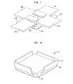
- FIGS. 4 , 4 A, 4 B, 4 C, 4 D, AND 4 Eare perspective views of a method of making the microelectronic package shown in FIG. 3 in accordance with one embodiment.
- FIG. 4Fis an embodiment showing the microelectronic package constructed in FIGS. 4A-4E attached to another device.
- FIGS. 5-5Aillustrate a microelectronic package in accordance with an alternative embodiment.
- FIGS. 6-6Aillustrate perspective views of steps in making a microelectronic package in accordance with another embodiment.
- FIGS. 7-7Aare perspective views of steps in making a microelectronic package in accordance with another embodiment.
- FIG. 8is a perspective view of an alternative microelectronic package.
- FIG. 9is a perspective view of an alternative microelectronic package.
- FIG. 10is a top plan view of the microelectronic package in accordance with another embodiment.
- FIG. 10Ais a cross-sectional view of FIG. 10 , taken along line 10 A- 10 A.
- FIG. 10Bis a cross-sectional view of FIG. 10 , taken along line 10 B- 10 B.
- FIG. 11is a cross-sectional view of a microelectronic package in accordance with another embodiment.
- FIG. 12is a cross-sectional view of a microelectronic package in accordance with another embodiment.
- FIG. 13is a cross-sectional view of a system in accordance with one embodiment.
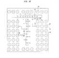
- FIG. 1illustrates a microelectronic package 100 in accordance with an embodiment of the present invention.
- microelectronic package 100includes a heat spreader 103 and one or more microelectronic elements encapsulated within an encapsulant, such as overmold 199 .
- FIG. 2Aa top plan view of FIG. 1 , as well as the corresponding cross-sectional views shown in FIGS. 2A-2B , provide further details of microelectronic package 100 .
- the overmold 199is not illustrated in the cross-sectional views shown in FIGS. 2A and 2B , the overmold 199 will be illustrated.
- microelectronic package 100includes first and second microelectronic elements 136 , 153 overlying a substrate 102 .
- the first and second microelectronic elements 136may be any type of semiconductor chips.
- the first and second microelectronic elements 136 , 153can be one which is configured to predominantly provide memory storage array function, i.e., one which has a greater number of active devices therein for providing memory storage array function than any other function.
- the microelectronic elementmay include a semiconductor chip implemented in one or more of the following techniques, DRAM (dynamic random access memory), NAND flash memory, resistive RAM (RRAM), phase-change memory (PCM), magnetroristive memory, spin-torque RAM, or serial access memory, among others.
- DRAMdynamic random access memory
- NAND flash memoryNAND flash memory
- RRAMresistive RAM
- PCMphase-change memory
- magnetroristive memorymagnetroristive memory
- spin-torque RAMspin-torque RAM
- serial access memoryamong others.
- the conductive elements of the first microelectronic elementsmay include first bond pads 142 that extend along the central region 950 of the front surface 140 of the first microelectronic element 136 . As best shown in FIG.
- the surface area of the front surface 140 of the first microelectronic element 136may be divided into three regions having substantially equal widths in a direction between the first and second edges of the first microelectronic element: a first outer region 920 , a second outer region 922 , and a central region 924 positioned between the first outer region 920 and second outer region 922 .
- a first outer region 920For example, if the length between the long edges is 6 microns, the respective lengths of the first outer, second outer, and central regions may be 2 microns.
- the central region 924would therefore be positioned 2 microns from the first edge 144 and 2 microns from the second edge 145 .
- the central region 924can be positioned in the middle third of the first microelectronic element 136 .
- the front surface 140faces and can be attached to the first surface 104 of the substrate 102 such as using an adhesive 117 or other bonding technique compatible with the materials of the microelectronic element and substrate.
- the second microelectronic element 153has opposed first and second edges 161 , 162 and opposed third and fourth edges 163 , 164 extending between the rear surface 155 and front surface 157 of the second microelectronic element 153 and adjacent first and second edges 161 , 162 .
- Conductive elementssuch as bond pads 159 , extend along the front surface 157 of the second microelectronic element 153 .
- the second microelectronic element 153may be a semiconductor chip, such as a DRAM chip, with bond pads 159 positioned along a central region 932 of the second microelectronic element 153 , which is positioned between a first outer region 928 and a second outer region 930 .
- bond pads 159can extend in a direction transverse to the direction bond pads 142 on the first microelectronic element 136 extend.
- the substrate 102can include a dielectric element of various types of construction, made of polymeric material or inorganic material such as ceramic or glass, the dielectric element having conductive elements thereon such as terminals and leads, e.g., traces, substrate contacts, or other conductive elements electrically connected with the terminals.
- the substrate 102can consist essentially of a semiconductor material such as silicon, or alternatively include a layer of semiconductor material and one or more dielectric layers thereof.
- the substratecan be a lead frame having leads, wherein the terminals can be portions of the leads, such as end portions of the leads.
- the substrate 102includes a first surface 104 and a second surface 106 remote therefrom. Although the thickness of the substrate 102 will vary with the application, the substrate 102 most typically is about 10 to 100 micrometers (microns) thick.
- the substrate 102may have conductive traces 108 and a plurality of terminals 110 , first set of contacts 109 , and second set of contacts 111 , exposed at a surface thereof.
- the terminalscan be electrically conductive contacts such as pads, posts, bumps, or other structure, and may include electrically conductive joining units 115 of a bond metal, e.g., solder tin, indium, gold, or other electrically conductive bond material for use in joining the package with another component such as contacts on a circuit panel.
- a statement that an electrically conductive element is “exposed at” a surface of a structureindicates that the electrically conductive element is available for contact with a theoretical point moving in a direction perpendicular to the surface toward the surface from outside the structure.
- a terminal or other conductive element which is exposed at a surface of a structuremay project from such surface; may be flush with such surface; or may be recessed relative to such surface and exposed through a hole or depression in the structure.
- Conductive tracessuch as conductive traces 108 ( FIG. 2D ), may be formed on the second surface 106 of substrate 102 from any electrically conductive material, but most typically are formed from copper, copper alloys, nickel, aluminum, or combinations of these materials. The thickness of the traces will also vary with the application, but typically is about 5 to 25 microns.
- the substrate 102 and traces 108can be fabricated by a process such as that disclosed in co-pending, commonly assigned U.S. Pat. No. 7,462,936, the disclosure of which is incorporated by reference herein.
- the substrate 102may further include at least two openings extending between the first surface 104 and second surface 106 of the substrate 102 .
- the first opening 116may be positioned near the central portion of the substrate 102 and have a pair of short edges 118 and a pair of long edges 120 that have a length L ( FIG. 2 ) that is greater than the length of the short edges 118 to define a longest dimension of the opening.
- a second opening 126may extend in a direction transverse to the first opening 116 .
- the second opening 126extends in a direction that is perpendicular to the first opening 116 , so that the first and second openings 116 , 126 form the shape of a T. It is to be appreciated that the first and second openings 116 , 126 may alternatively be joined together to form one continuous opening. In another alternative embodiment, the first opening 116 or second opening 126 may be comprised of a plurality of openings, such that the first opening 116 is alternatively a plurality of openings arranged, i.e., spaced apart from one another, in one direction parallel to the surface 106 , and the second opening 126 is alternatively a plurality of openings which are spaced apart from one another in a direction transverse to the first opening 116 . It is to be further appreciated that the openings may also take on any alternative shape or design.
- first microelectronic element 136 and second microelectronic element 153are stacked in face-down positions, such that at least a portion of the second microelectronic element 153 overlies a rear surface 138 ( FIG. 2A ) of first microelectronic element 136 .
- Front surface 140includes a plurality of bond pads or contacts 142 exposed thereat.
- the front face 140faces and can be attached to the first surface 104 of the substrate 102 such as using an adhesive 117 or other bonding technique compatible with the materials of the microelectronic element and substrate.
- the bond pads 142 of the first microelectronic element 136may be positioned directly over the first opening 116 of the substrate 102 . This allows the bond pads 142 to be exposed through the first opening 116 .
- the bond pads 142may be electrically connected to a first set of contacts 109 on the second surface 106 of the substrate 102 .
- wire bonds 148can extend from the bond pads 142 on the first microelectronic element 136 , through the first opening 116 , and to the first set of contacts 109 on the second surface 106 of the substrate 102 .
- Traces 108( FIG. 3 ) can be used to connect the first set of contacts 109 to the terminals 110 .
- a heat spreader 103may overlie the first microelectronic element 136 .
- a spacer 135( FIG. 2B ) may be positioned between the substrate 102 and the heat spreader 103 to support the heat spreader 103 at a height above the surface 104 of the substrate.
- a top plan view of the heat spreader standing alone, heat spreader 103can be a continuous, planar, and sheet-like element. Heat spreader 103 is in the shape of a cross, but any desired shape, such as round, triangle, square, or rectangular, may be considered.
- Heat spreader 103includes outer edges 103 A, 103 B, 103 C, 103 D and at least one aperture 101 that extends between the first and second surfaces 105 , 107 (FIGS. 2 A, 2 B, 2 E).
- the aperture 101should be positioned so that all or a portion of the aperture 101 can be aligned with second opening 126 . This will enable wire bonds extending from an overlying microelectronic element, such as the second microelectronic element 153 , to pass therethrough, as will be discussed in greater deal herein.
- the heat spreader 103may be partly or entirely made of any suitable thermally conductive material.
- suitable thermally conductive materialinclude, but are not limited to, metal, graphite, thermally conductive adhesives, e.g., thermally conductive epoxy, a solder, or the like, or a combination of such materials.
- heat spreader 103is attached to or disposed on the rear surface 138 of the first microelectronic element 136 , such as with a thermally conductive material such as a thermally conductive adhesive or thermally conductive grease.
- the adhesiveif present, can be a compliant material which permits relative movement between the heat spreader and the microelectronic element to which it is attached, such as to accommodate differential thermal expansion between the compliantly attached elements.
- the heat spreader 103may also contact second microelectronic element 153 .
- the heat spreader 103may be a monolithic structure. Alternatively, the heat spreader 103 may include multiple spreader portions spaced apart from one another. In a particular embodiment, the heat spreader 103 may be or include a layer of solder joined directly to at least a portion of a rear surface 138 of the first microelectronic element 136 .
- one or more edges 103 A, 103 B, 103 C, 103 D of the heat spreader 102should be aligned with at least one edge 102 A, 102 B, 102 C, 102 D of the substrate 102 .
- each of the edges 103 A, 103 B, 103 C, 103 D of the heat spreader 103will be aligned with the respective edges 102 A, 102 B, 102 C, 102 D of the substrate 102 .
- one or more edges of the heat spreader 103will not be aligned with edges of the substrate.
- heat spreader 103can take on a variety of configurations.
- edgesmay extend upward, downward, around the edges of microelectronic elements or other devices within the microelectronic package, or any desired configuration. It may also be desired for the heat spreader 103 to have a non-planar configuration or for the heat spreader to be comprised of one or more panels or sheets.
- Conductive elementssuch as bond pads 159 also extend along the front surface 157 of the second microelectronic element 153 .
- the second microelectronic element 153may also be a semiconductor chip, such as a DRAM chip, with bond pads 159 positioned along a central region 952 of the second microelectronic element 153 .
- bond pads 159can extend in a direction transverse to the direction bond pads 142 on the first microelectronic element 136 extend.
- bond pads 159 on the second microelectronic element 153may be electrically connected with a second set of contacts 111 of the plurality of contacts exposed at the second surface 106 of substrate 102 .
- Conductive elementsmay be used to electrically connect the bond pads 159 on the second microelectronic element 153 with the substrate 102 .
- electrical connectionssuch as wire bonds 165 may be used to couple the bond pads 159 on the second microelectronic element 153 with the terminals 110 through the second set of contacts 111 exposed at the second surface 106 of the substrate 102 .
- wire bonds 165extend through the second opening 126 and connect to the second set of contacts 111 .
- traces 112can extend from the second set of contacts 111 along the second surface 106 and be electrically connected with terminals 110 .
- an overmold 199may overlie some or all of the first surface 104 of the substrate 102 , and the first and second microelectronic elements 136 , 153 , and may cover wire bonds 148 , 165 extending through the respective first opening 116 and second opening 126 .
- FIGS. 2 A, 2 B.edges 103 A- 103 D of the heat spreader 103 are aligned with respective edges 102 A- 102 D of the substrate in respective directions 122 , 124 parallel to the surface 104 of the substrate, as shown in FIGS. 1 and 2 , edges 103 A- 103 D of the heat spreader 103 can be exposed at edges of the overmold 199 .
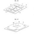
- FIGS. 3-3Dthere is shown a microelectronic package incorporating a heat spreader 203 in accordance with an alternative embodiment.
- FIG. 3a top plan view of the microelectronic package 200 is shown. It is to be appreciated that for ease of discussion and illustration, microelectronic package 200 , illustrated in FIG. 3 , does not show the presence of the encapsulant (see FIG. 3A ), which encapsulates each of the components of the microelectronic package. However, subsequent views, shown in FIGS. 3A-D , will illustrate the presence of the encapsulant.
- Microelectronic package 200includes two lower microelectronic elements (first and second microelectronic elements) and two upper and stacked microelectronic elements (third and fourth microelectronic elements), all of which overlie a substrate 202 in a face-down position.
- first and second openings 216 , 226extend between the first and second surfaces 204 , 206 of the substrate 202 .
- the first and second openings 216 , 226are parallel to one another and both extend in a direction that is perpendicular or normal to the direction the third and fourth openings 232 , 282 extend.
- the first opening 216has long edges 220 and short edges 218 , wherein the short edges 218 are located at a first end 222 and a second end 224 of the first opening 216 .
- the second opening 226also has a pair of short edges 228 and a pair of long edges 230 , wherein the short edges 228 are respectively located at a first end 229 and a second end 231 of the second opening 226 .
- the third opening 232is located adjacent the respective first ends 222 , 229 of the first and second openings 216 , 226
- the fourth opening 282is located adjacent the respective second ends 224 , 231 of the first and second openings 216 , 226
- the respective long edges 234 , 284 of the third and fourth openings 232 , 282are not aligned with the long edges 220 , 230 of the respective first and second openings 216 , 226 .
- the first and second openings 216 , 226are spaced further away from the outer peripheral edge 212 of the substrate 202 than the third and fourth openings 232 , 282 .
- the front surface 240 , 257 of the first and second microelectronic elements 236 , 253may each be attached to the substrate 202 such as with an adhesive 217 or other suitable bonding technique with the first microelectronic element 236 and the second microelectronic element 253 spaced apart from one another in a direction along the first surface 204 of the substrate 202 .
- Bond pads 242 on the first microelectronic element 236may be aligned with the first opening 216
- bond pads 259 on the second microelectronic element 253may be aligned with the second opening 226 so that the bond pads of each, microelectronic element 236 , 253 are exposed through the respective opening 216 , 226 .
- the first and second edges 244 , 245 of the first microelectronic element 236 and the first and second edges 261 , 262 of the second microelectronic element 253are parallel to one another and extend in the same direction.
- Heat spreader 203overlies the rear surface 238 of the first microelectronic element 236 , as well as the rear surface 255 of the second microelectronic element 253 .
- one or more spacers 235may be used to support the portions of the heat spreader 203 that face toward the substrate 202 , but do not overlie the first and/or second microelectronic elements 236 , 253 .
- each of the edges 203 A- 203 D ( FIG. 3 ) of the heat spreaderwill be aligned with the edges 202 A- 202 D of the substrate 202 .
- heat spreader 203can take on a variety of alternative embodiments, including those wherein the edges of the heat spreader are not aligned with edges of the substrate 202 .
- the third and fourth microelectronic elements 268 , 288may be positioned to overlie the substrate 202 , first and second microelectronic elements 236 , 253 , and heat spreader 203 . As best shown in FIGS. 3 and 3A , front surface 272 of the third microelectronic element 268 directly overlies the first surface 205 of the heat spreader 203 , as well as the rear surfaces 238 , 255 of the first and second microelectronic elements 236 , 253 .
- the front surface 292 of the fourth microelectronic element 288overlies the first surface 205 of the heat spreader 203 , as well as the rear surfaces 238 , 255 of the respective first and second microelectronic elements 236 , 253 .
- the third microelectronic element 268is adjacent the respective first ends 237 , 251 of the first and second microelectronic elements 236 , 253 .
- the fourth microelectronic element 288is adjacent the second ends 250 , 267 of the respective first and second microelectronic elements 236 , 253 .
- first and second edges 276 , 277 of the third microelectronic element 268 and first and second edges 296 , 297 of the fourth microelectronic element 288extend in a direction that is perpendicular to both the respective first and second edges 244 , 245 of the first microelectronic element 236 and first and second edges 261 , 262 of the second microelectronic element 253 .
- the fourth microelectronic element 288will extend in a direction that is perpendicular to the respective bond pads 242 , 259 positioned near the respective central regions 950 , 952 of the respective first and second microelectronic elements 236 , 253 .
- the orientation of the heat spreader 203 overlying the first and second microelectronic elements 236 , 253 and underlying the third and fourth microelectronic elements 268 , 288will allow for an electrical connection between the bond pads 242 ( FIG. 3D ), 259 ( FIG. 3B ), 274 , 294 of the first, second, third, and fourth microelectronic elements 236 , 253 , 268 , 288 to the respective first, second, third, and fourth sets of contacts 209 , 211 , 213 , 214 on the second surface 206 of the substrate 202 .
- the electrical connectioncan be within or through the first, second, third, and fourth openings 216 , 226 , 232 , 282 .
- wire bonds 248 , 265 ( FIG. 3A ), 269 , 270 ( FIG. 3B ) extending from the respective first, second, third, and fourth microelectronic elements 236 , 253 , 268 , 288extend through the first, second, third, and fourth openings 216 , 226 , 232 , 282 , and connect to respective first, second, third, and fourth sets of contacts 209 , 211 , 213 , 214 on the substrate 202 (FIGS. 3 A, 3 B).
- traces 208 extending in a direction parallel to the second surface 206 of the substrate 202can connect the first, second, third, and fourth sets of contacts 209 , 211 , 213 , 214 to terminals exposed at the second surface.
- first, second, third and fourth openings 216 , 227 , 232 , 282can be provided within the substrate 202 that extend between the first and second surfaces 204 , 206 .
- first and second openings 216 , 227are spaced apart and parallel to one another.
- Third and fourth openings 232 , 282are also spaced apart and parallel to one another.
- first and second openings 216 , 227extend in a direction perpendicular to the direction third and fourth openings 232 , 282 extend, such that, in this embodiment, the openings can form the shape of a square.
- spacers 235can be provided adjacent the opposed outer edges 202 A-D of the substrate 202 , as well as adjacent the third and fourth openings 232 , 282 .
- spacers 235have a length L 1 that is greater than the length L 2 of the third and fourth openings.
- first and second microelectronic elements 236 , 253are provided on the first surface 204 of the substrate 202 .
- First and second microelectronic elements 236 , 253will be arranged so that the central bond pads 242 ( FIG. 3D ) of the first microelectronic element 236 are aligned with the first opening 216 and the central bond pads 259 of the second microelectronic element 253 are aligned with the second opening 226 .
- the heat spreader 202 shown in FIG. 4Cmay overlie spacers 235 , and respective rear surfaces 238 , 255 of the first and second microelectronic elements 236 , 253 .
- the heat spreader 203is in the shape of a cross. Each of the edges 203 A-D of the heat spreader 203 will be aligned with the edges 202 A-D of the substrate 202 .
- First and second openings 232 A, 282 A in the heat spreader 203extend between the first and second surfaces 205 , 207 ( FIG. 3A ) of the heat spreader 203 .
- the first opening 232 Awill be aligned with the third opening 232 in the substrate 202 to allow for wire bonds 269 to extend therethrough.
- the second opening 282 Awill be similarly aligned with the fourth opening 282 in the substrate 202 to allow wire bonds 270 to extend therethrough.
- third and fourth microelectronic elements 268 , 288are provided over the heat spreader 203 in a face-down position. Bond pads 274 ( FIG. 3B ) of the third microelectronic element 268 are aligned with the first opening 232 A ( FIG. 4C ) in the heat spreader 203 , as well as the third opening 232 ( FIG. 4A ) in the substrate 202 .
- bond pads 294 ( FIG. 3B ) of the fourth microelectronic element 288are aligned with the second opening 282 A in the heat spreader 203 , as well as the fourth opening 282 ( FIG. 4C ) in the substrate 202 ( FIG. 4 ).
- Wire bondsmay then be provided to electrically connect the first and second microelectronic elements with contacts on the second surface 206 of the substrate, as well as to electrically connect the third and fourth microelectronic elements 268 , 288 with contacts on the second surface of the substrate 202 .
- an encapsulantmay then be provided over each of the components, including the substrate 202 , heat spreader 203 , and first through fourth microelectronic elements 236 , 253 , 268 , 288 , to provide a microelectronic package 200 .
- the heat spreader 203may be aligned with the outer edge 298 of the overmold 299 , such that the outer edges 203 A (not shown), 203 B, 203 C, and 203 D (not shown) may be exposed.
- the microelectronic package 200may then be electrically connected with another device, such as, for example, the printed circuit board 289 shown in FIG. 4F .
- the heat spreadercan take on any desired configuration.
- one or more of the outer edges of the heat spreader 303do not align with the substrate 302 .
- each of the edges 303 A- 303 D of the heat spreaderare spaced back from the corresponding adjacent outer edge 302 A- 302 D of the substrate 302 in a direction 310 or 312 parallel to the surface 304 of the substrate and away from such edge of the substrate.
- the edges 303 A- 303 D of the heat spreader 303will be fully encapsulated by the overmold and the heat spreader 303 will not be exposed to the atmosphere. As shown, the overmold will extend continuously around the microelectronic package 300 .
- a heat spreader 403is provided wherein some of the edges 403 A, 403 C, 403 D are aligned with the edges of the spacers 435 and the heat spreader 403 has one flap 403 B or edge that extends downward toward the substrate 402 .
- the flap 403 B extending toward the substrate 402can therefore be in thermal communication with the substrate. Because none of the edges 403 A-D of the heat spreader 403 extend to the outermost edge of the substrate 402 , upon encapsulation, the heat spreader 403 is not exposed to the atmosphere. Thus, the edges 403 A-D will not be exposed beyond the edge 498 of the overmold 499 , as best seen in the encapsulated microelectronic package 400 , shown in FIG. 6A .
- an alternative heat spreader 503is shown with flaps 503 A-D extending beyond the edges 502 A-D of the substrate 502 .
- the flaps 503 A-Dwill extend beyond the edges of the overmold 599 .
- the flaps 503 A-Dmay be formed to point upwards.
- one or more flaps 503 A-D′ of the heat spreader 503 ′ extending beyond the edge 598 of the overmold 599 ′may instead extend downwardly toward the second surface 506 of the substrate 502 .
- the flaps 503 A, 503 B, 503 C, 503 Dmay be thermally and mechanically affixed to the substrate such as with a bond metal or a thermally conductive adhesive.
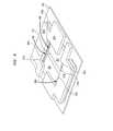
- FIG. 9another alternative embodiment is shown.
- This embodimentis similar to the embodiment shown in FIGS. 4-4F , except that instead of only one heat spreader, there are two: a first heat spreader 303 A and an adjacent second heat spreader 303 B.
- the first heat spreader 303 A and second heat spreader 303 Bare separated, thereby creating a first opening 385 between them.
- the first heat spreader 303 A and second heat spreader 303 Bare mirror images of one another, but they may take on any shape or configuration in alternative embodiments.
- First and second microelectronic elements 336 ′, 353 ′ directly adjacent the substrate 302 ′are exposed through the first opening 385 .
- a second opening 386is created between the inner edge 385 A of the first heat spreader 303 A and the respective edges 378 A, 379 A of the first and second microelectronic elements 336 ′, 353 ′.
- the second opening 385is aligned with the opening 232 in the substrate 302 ′.
- a third opening 386is created between the edge 385 B of the second heat spreader 303 B and the opposed edges 378 B, 379 B of the first and second microlectronic elements 336 ′, 353 ′.
- the third opening 386 Ais also aligned with the opening (not shown; see opening 282 in FIG. 4A ) in the substrate 302 ′.
- third and fourth microelectronic elementsmay be provided over the first and second heat spreaders 303 A, 303 B, and an overmold (not shown) can be provided over the entire assembly.
- FIGS. 10 , 10 A, 10 Ban alternative microelectronic package 600 is shown.
- This embodimentis identical to the microelectronic package 200 shown in FIGS. 3-3D , except that there is a second heat spreader 603 ′ overlying the third and fourth microelectronic elements 668 , 688 .
- this embodimentonly the outer edges 603 ′A, 603 ′C of the second heat spreader 603 ′ are aligned with the edges 602 A- 602 D of the substrate 602 or the edge 698 of the overmold 699 .
- FIG. 10 , 10 A, 10 Ban alternative microelectronic package 600 is shown.
- This embodimentis identical to the microelectronic package 200 shown in FIGS. 3-3D , except that there is a second heat spreader 603 ′ overlying the third and fourth microelectronic elements 668 , 688 .
- edges 603 ′B, 603 ′D of the second heat spreader 603 ′are spaced a distance L away from the edges 602 B, 602 D of the substrate 602 and the edge 698 of the overmold 699 .
- the second heat spreadercan take on any one of a variety of shapes or configurations.
- the microelectronic element closest to the substrate 702may be configured to overlie the substrate 702 in a variety of configurations, such as a flip chip orientation, or a face-up orientation.
- the microelectronic assembly 700may include a bond element which electrically connects bond pads 759 of the second microelectronic element 753 to the terminals 710 of the substrate 702 .
- leadscan include bond elements 765 such as wire bonds which extend through aperture 716 and are bonded to bond pads 759 of the second microelectronic element 753 and the substrate 702 .
- the bond wires 765are at least partially aligned with the opening 716 of the substrate 702 .
- the wire bond 765may include multiple wire bonds 765 electrically connecting some bond pads of the second microelectronic element 753 with conductive elements 709 exposed at the substrate 702 .
- Wire bonds 748 , 749extend through the opening 716 .
- Each of the wire bonds 748 and 749electrically couples a bond pad 759 to a corresponding conductive element 747 of the dielectric element 702 .
- the bond wires 765may include a multiple wire bond structure as described in U.S. patent application Ser. No. 12/907,522 filed Oct. 19, 2010, and entitled “Enhanced Stacked Microelectronic Assemblies with Central Contacts and Improved Thermal Characteristics,” the entire disclosure of which is incorporated herein by reference. As seen in FIG.
- leadssuch as lead bonds 751 may extend along the first surface 704 of the substrate 702 as shown or along the second surface and into the aperture 716 to electrically connect to bond pads 759 .
- the lead bonds 751do not necessarily extend through the opening 716 of the dielectric element 702 but are at least partially aligned with the opening 716 .
- the microelectronic assembly 700may further include an overmold or encapsulant 799 covering at least the first microelectronic element 736 and the second microelectronic element 753 .
- the overmold 799may also cover portions of the substrate 702 extending beyond the first edge 737 of the first microelectronic element 736 and the first edge 761 of the second microelectronic element 753 . Consequently, the overmold 799 may contact at least the first edge 737 of the first microelectronic element 736 , the first edge 761 of the second microelectronic element 753 , and the first surface 704 of the dielectric element 702 .
- the overmold 799may be made from any suitable material, including epoxy and the like.
- the microelectronic assembly 700may additionally include a heat spreader or heat sink attached to the rear surfaces of one or more of the first or second microelectronic elements 736 , 753 , as described in U.S. patent application Ser. No. 12/907,522 filed Oct. 19, 2010, and entitled “Enhanced Stacked Microelectronic Assemblies with Central Contacts and Improved Thermal Characteristics,” the entire disclosure of which is hereby incorporated herein by reference.
- the microelectronic assembly 700includes a heat spreader thermally coupled to the first and/or second microelectronic elements 736 , 753 but does not include an overmold 11 .
- the microelectronic assembly 700may further include joining units 715 attached to terminals 710 on the second surface 706 of the substrate 702 .
- the joining units 710may be solder balls or other masses of bond and metal, e.g., tin, indium, or a combination thereof, and are adapted to join and electrically couple the microelectronic assembly 700 to a circuit panel, such as a printed circuit board.
- FIG. 12depicts a variation of the microelectronic assembly 700 shown in FIG. 11 .
- the first microelectronic element 736 ′may be positioned so that the surface 740 ′ is a front surface facing away from the substrate 702 ′.
- Surface 740 ′may have a first end portion 790 adjacent the first edge 737 ′ of the first microelectronic element 736 ′, a second end portion 791 adjacent the second edge 745 ′, and a central portion 793 between the first and second end portions 790 and 791 .
- the bond pads or contacts 742 ′may be disposed within the first end portion 790 of the surface 740 ′ adjacent the first edge 737 ′, within the central portion 793 of the surface 740 ′, or within both the first end portion 790 and central portion 793 . In one embodiment, the contacts 742 ′ may be arranged in one or two parallel rows at the central portion 793 of the surface 740 ′.
- the microelectronic assembly 700 ′can further include leads 749 ′ electrically connected with the contacts 742 ′ at the surface 740 ′ and with the terminals 710 ′.
- portions of the leads 749 ′such as wire bonds can extend beyond the first edge 737 ′ of the first microelectronic element 736 ′ to contacts 757 A, 757 B, which in turn, can be connected to terminals 710 ′, such as through traces (not shown) or other conductive elements.
- the leads 749 B′may include wire bonds extending from the contacts 742 ′, beyond the first edge 737 ′ of the first microelectronic element 736 ′, and to contacts 757 A at the first surface 704 ′ of the substrate 702 ′, and may include other conductive structure of the substrate such as conductive traces between the contacts and the terminals 710 ′.
- lead portions 748 ′e.g., wire bonds can connect contacts 758 of microelectronic element 753 ′ to contacts 709 ′ adjacent the aperture 716 ′.
- a heat spreader 703 ′may be positioned between the first microelectronic element and the second microelectronic element 753 ′.
- the heat spreaderwill have openings to allow for the lead wires 749 ′, 748 ′ to extend therethrough.
- a system 800 in accordance with a further embodiment of the inventionincludes a structure 806 as described in the prior embodiments of microelectronic assemblies above in conjunction with other electronic components 808 and 810 .
- component 808is a semiconductor chip
- component 810is a display screen, but any other components can be used.
- the structure 806as described above, may be, for example, a composite chip or a structure incorporating plural chips.
- bothmay be provided, and any number of such structures may be used.
- Structure 806 and components 808 and 810are mounted in a common housing 801 , schematically depicted in broken lines, and are electrically interconnected with one another as necessary to form the desired circuit.
- the systemincludes a circuit panel 802 such as a flexible printed circuit board, and the circuit panel includes numerous conductors 804 , of which only one is depicted in FIG. 13 , interconnecting the components with one another.
- thisis merely exemplary; any suitable structure for making electrical connections can be used.
- the housing 801is depicted as a portable housing of the type usable, for example, in a cellular telephone or personal digital assistant, and screen 810 is exposed at the surface of the housing.
- structure 706includes a light-sensitive element such as an imaging chip
- a lens 711 or other optical devicealso may be provided for routing light to the structure.
- FIG. 13the simplified system shown in FIG. 13 is merely exemplary; other systems, including systems commonly regarded as fixed structures, such as desktop computers, routers, and the like, can be made using the structures discussed above.
- terms such as “upper,” “lower,” “upwardly,” and “downwardly,” and similar terms denoting directionsrefer to the frame of reference of the components themselves, rather than to the gravitational frame of reference.
- the upper substrateis, indeed, above the lower substrate in the gravitational frame of reference.
- the upper substrateis below the lower substrate in the gravitational frame of reference.
Landscapes
- Engineering & Computer Science (AREA)
- Microelectronics & Electronic Packaging (AREA)
- Power Engineering (AREA)
- Physics & Mathematics (AREA)
- Condensed Matter Physics & Semiconductors (AREA)
- General Physics & Mathematics (AREA)
- Computer Hardware Design (AREA)
- Chemical & Material Sciences (AREA)
- Materials Engineering (AREA)
- Cooling Or The Like Of Semiconductors Or Solid State Devices (AREA)
- Wire Bonding (AREA)
Abstract
Description
- This application relates to commonly owned U.S. Provisional Patent Application No. 61/477,877 entitled “Multiple Die Face-Down Stacking For Two Or More Die” and filed on Apr. 21, 2011, the disclosure of which is incorporated herein by reference.
- The subject matter of the present application relates to microelectronic packages and assemblies, particularly such packages and assemblies which incorporate a heat spreader.
- Microelectronic devices generally comprise a thin slab of a semiconductor material, such as silicon or gallium arsenide, commonly called a die or a semiconductor chip. Semiconductor chips are commonly provided as individual, prepackaged units. The active circuitry is fabricated in a first face of the semiconductor chip (e.g., a front surface). To facilitate electrical connection to the active circuitry, the chip is provided with bond pads on the same face. The bond pads are typically placed in a regular array either around the edges of the die or, for many memory devices, in the die center. The bond pads are generally made of a conductive metal, such as copper or aluminum that is approximately 0.5 microns (μm) thick. The bond pads could include a single layer or multiple layers of metal. The size of the bond pads will vary with the device type, but will typically measure tens to hundreds of microns on a side.
- Semiconductor chips are commonly provided in packages that facilitate handling of the chip during manufacture and during mounting of the chip on an external substrate such as a circuit board or other circuit panel. For example, many semiconductor chips are provided in packages suitable for surface mounting. Numerous packages of this general type have been proposed for various applications. Most commonly, such packages include a substrate, commonly referred to as a “chip carrier” with terminals formed as plated or etched metallic structures on the dielectric. These terminals typically are connected to the contacts of the chip itself by features such as thin traces extending along the chip carrier itself and by fine leads or wires extending between the contacts of the chip and the terminals or traces. In a surface mounting operation, the package is placed onto a circuit board so that each terminal on the package is aligned with a corresponding contact pad on the circuit board. Solder or other bonding material is provided between the terminals and the contact pads. The package can be permanently bonded in place by heating the assembly so as to melt or “reflow” the solder or otherwise activate the bonding material.
- Despite the various improvements made in the art, further improvements would be desirable in the case of multi-chip packages, particularly for chips having contacts located in central regions of the chips. Certain semiconductor chips, such as some memory chips, are commonly made with the contacts in one or two rows located in a central region of the chip.
- In accordance with one aspect of the present invention, there is a microelectronic package that includes a substrate, first and second microelectronic elements, and a heat spreader. There are terminals exposed at the substrate configured for electrical connection with a component external to the package. The first microelectronic element may be adjacent the substrate and a second microelectronic element at least partially overlies the first microelectronic element. A sheet-like heat spreader has an aperture and separates the first and second microelectronic elements. Connection may extend through the aperture and electrically couple the second microelectronic element with the substrate.
- In one embodiment, there is a third microelectronic element adjacent the substrate and the second microelectronic element partially overlies the third microelectronic element.
- In another embodiment, a fourth microelectronic element at least partially overlies at least one of the first or third microelectronic elements. The heat spreader further includes a second aperture. Second connections may extend through the second aperture and electrically couple the fourth microelectronic element with the substrate.
- In another embodiment, the first and second apertures are parallel to one another. Alternatively, the first and second apertures are normal to one another.
- In an alternative embodiment, the substrate includes an aperture and connections that include leads having portions aligned with the aperture of the substrate. Alternatively, the leads are wire bonds extending through the aperture of the substrate.
- In another embodiment, the heat spreader includes a metal foil. Alternatively, the heat spreader has a first surface facing the second microelectronic element and peripheral edges bounding the first surface. The package further comprises an overmold overlying the substrate, the first and second microelectronic elements, and a portion of the heat spreader. The heat spreader may be exposed at at least one of the peripheral edges of the overmold.
- In another embodiment, the heat spreader extends beyond two edges of the overmold. Alternatively, the heat spreader extends beyond four edges of the overmold. In another alternative embodiment, at least one peripheral edge of the heat spreader is exposed at and flush with the at least one peripheral edge of the overmold. Alternatively, the heat spreader may not extend beyond the peripheral edges of the overmold.
- In another embodiment, at least a portion of the heat spreader is bent in a direction of the substrate. The heat spreader may be bent in a direction away from the substrate or toward the substrate.
- In one embodiment, the heat spreader is in thermal communication with the first and second microelectronic elements. Alternatively, the heat spreader may be in thermal contact with a portion of at least one of the first or second microelectronic elements or only the first microelectronic element or only the second microelectronic element. In another embodiment, an assembly includes any of the packages disclosed herein and a circuit panel. The package may be electrically interconnected with the circuit panel and the heat spreader may be joined to the circuit panel.
- In accordance with another aspect of the present invention, there is a microelectronic package that includes a substrate, first and second microelectronic elements, and first and second heat spreaders. Terminals may be exposed at the substrate configured for electrical connection with a component external to the package. The first microelectronic element may be adjacent the substrate and a second microelectronic element at least partially overlies the first microelectronic element. A sheet-like heat spreader has an aperture and separates the first and second microelectronic elements. Connection may extend through the aperture and electrically couple the second microelectronic element with the substrate. Alternatively, the package may be electrically interconnected with the circuit panel and the heat spreader joined to the circuit panel.
- In another aspect of the present invention, there is a system that comprises a microelectronic package, according to any of the abovementioned aspects, and one or more other electronic components electrically connected with the assembly. In an alternative embodiment, there is also a housing, and the microelectronic package and the other electronic components may be mounted to the housing.
- In yet another aspect of the present invention, there is a method of making the microelectronic packages disclosed herein that includes the steps of providing a substrate that has terminals thereon that is configured for electrical connection with a component external to the package; arranging a first microelectronic element adjacent the substrate and a second microelectronic element at least partially overlying the first microelectronic element; providing a sheet-like heat spreader with an aperture and positioning the heat spreader between the first and second microelectronic elements; and electrically connecting the second microelectronic element with the substrate using connections extending through the aperture.
- In another embodiment, a third microelectronic element is positioned adjacent the substrate so that the second microelectronic element partially overlies the third microelectronic element.
- In an alternative embodiment, a fourth microelectronic element may be arranged within the microelectronic package so that the at least fourth microelectronic element partially overlies at least one of the first or third microelectronic elements. Additionally, the fourth microelectronic element may be electrically connected with the substrate using second connections extending through a second aperture within the heat spreader.
- In another embodiment, the first and second apertures are parallel to one another. Alternatively, the first and second apertures are normal to one another.
FIG. 1 is a perspective view of a microelectronic package in accordance with one embodiment.FIG. 2 is a top plan view of the microelectronic package shown inFIG. 1 .FIG. 2A is a cross-sectional view of the microelectronic package shown inFIG. 2 , taken alongline 2A-2A.FIG. 2B is a cross-sectional view ofFIG. 2 , taken alongline 2B-2B.FIG. 2C is a top plan view of the front surface of a microelectronic element shown inFIG. 2 .FIG. 2D is a top plan view of the front surface of another microelectronic element shown inFIG. 2 .FIG. 2E is a bottom plan view of the microelectronic package shown inFIG. 1 .FIG. 2F is a top plan view of a heat spreader in accordance with one embodiment of the invention.FIG. 3 is a top plan view of a microelectronic package in accordance with an alternative embodiment.FIG. 3A is a cross-sectional view ofFIG. 3 , taken alongline 3A-3A.FIG. 3B is a cross-sectional view ofFIG. 3 , taken alongline 3B-3B.FIG. 3C is a cross-sectional view ofFIG. 3 , taken alongline 3C-3C.FIG. 3D is a cross-sectional view ofFIG. 3 , taken alongline 3D-3D.FIG. 3E is a bottom plan view ofFIG. 2 .- FIGS.4,4A,4B,4C,4D, AND4E are perspective views of a method of making the microelectronic package shown in
FIG. 3 in accordance with one embodiment. FIG. 4F is an embodiment showing the microelectronic package constructed inFIGS. 4A-4E attached to another device.FIGS. 5-5A illustrate a microelectronic package in accordance with an alternative embodiment.FIGS. 6-6A illustrate perspective views of steps in making a microelectronic package in accordance with another embodiment.FIGS. 7-7A are perspective views of steps in making a microelectronic package in accordance with another embodiment.FIG. 8 is a perspective view of an alternative microelectronic package.FIG. 9 is a perspective view of an alternative microelectronic package.FIG. 10 is a top plan view of the microelectronic package in accordance with another embodiment.FIG. 10A is a cross-sectional view ofFIG. 10 , taken along line10A-10A.FIG. 10B is a cross-sectional view ofFIG. 10 , taken along line10B-10B.FIG. 11 is a cross-sectional view of a microelectronic package in accordance with another embodiment.FIG. 12 is a cross-sectional view of a microelectronic package in accordance with another embodiment.FIG. 13 is a cross-sectional view of a system in accordance with one embodiment.FIG. 1 illustrates amicroelectronic package 100 in accordance with an embodiment of the present invention. In this embodiment,microelectronic package 100 includes aheat spreader 103 and one or more microelectronic elements encapsulated within an encapsulant, such asovermold 199.FIG. 2A , a top plan view ofFIG. 1 , as well as the corresponding cross-sectional views shown inFIGS. 2A-2B , provide further details ofmicroelectronic package 100. It is to be appreciated that in the top plan view ofFIG. 2A , to better illustrate the stacked arrangement of the components within themicroelectronic package 100, theovermold 199 is not illustrated. However, in the cross-sectional views shown inFIGS. 2A and 2B , theovermold 199 will be illustrated.- With reference now to
FIGS. 2 and 2A ,microelectronic package 100 includes first and secondmicroelectronic elements substrate 102. The first and secondmicroelectronic elements 136 may be any type of semiconductor chips. In a particular embodiment, the first and secondmicroelectronic elements first bond pads 142 that extend along thecentral region 950 of thefront surface 140 of the firstmicroelectronic element 136. As best shown inFIG. 2C , the surface area of thefront surface 140 of the firstmicroelectronic element 136 may be divided into three regions having substantially equal widths in a direction between the first and second edges of the first microelectronic element: a firstouter region 920, a secondouter region 922, and acentral region 924 positioned between the firstouter region 920 and secondouter region 922. For example, if the length between the long edges is 6 microns, the respective lengths of the first outer, second outer, and central regions may be 2 microns. Thecentral region 924 would therefore be positioned 2 microns from thefirst edge 144 and 2 microns from thesecond edge 145. In other words, thecentral region 924 can be positioned in the middle third of the firstmicroelectronic element 136. Thefront surface 140 faces and can be attached to thefirst surface 104 of thesubstrate 102 such as using an adhesive117 or other bonding technique compatible with the materials of the microelectronic element and substrate. - Similarly, the second
microelectronic element 153 has opposed first andsecond edges fourth edges rear surface 155 andfront surface 157 of the secondmicroelectronic element 153 and adjacent first andsecond edges bond pads 159, extend along thefront surface 157 of the secondmicroelectronic element 153. In this embodiment, the secondmicroelectronic element 153 may be a semiconductor chip, such as a DRAM chip, withbond pads 159 positioned along acentral region 932 of the secondmicroelectronic element 153, which is positioned between a firstouter region 928 and a secondouter region 930. In one embodiment,bond pads 159 can extend in a direction transverse to thedirection bond pads 142 on the firstmicroelectronic element 136 extend. - In particular embodiments, the
substrate 102 can include a dielectric element of various types of construction, made of polymeric material or inorganic material such as ceramic or glass, the dielectric element having conductive elements thereon such as terminals and leads, e.g., traces, substrate contacts, or other conductive elements electrically connected with the terminals. In another example, thesubstrate 102 can consist essentially of a semiconductor material such as silicon, or alternatively include a layer of semiconductor material and one or more dielectric layers thereof. In yet another embodiment, the substrate can be a lead frame having leads, wherein the terminals can be portions of the leads, such as end portions of the leads. - As best shown in
FIGS. 2A and 2B , thesubstrate 102 includes afirst surface 104 and asecond surface 106 remote therefrom. Although the thickness of thesubstrate 102 will vary with the application, thesubstrate 102 most typically is about 10 to 100 micrometers (microns) thick. Thesubstrate 102 may haveconductive traces 108 and a plurality ofterminals 110, first set ofcontacts 109, and second set ofcontacts 111, exposed at a surface thereof. The terminals can be electrically conductive contacts such as pads, posts, bumps, or other structure, and may include electrically conductive joiningunits 115 of a bond metal, e.g., solder tin, indium, gold, or other electrically conductive bond material for use in joining the package with another component such as contacts on a circuit panel. As used in this disclosure, a statement that an electrically conductive element is “exposed at” a surface of a structure indicates that the electrically conductive element is available for contact with a theoretical point moving in a direction perpendicular to the surface toward the surface from outside the structure. Thus, a terminal or other conductive element which is exposed at a surface of a structure may project from such surface; may be flush with such surface; or may be recessed relative to such surface and exposed through a hole or depression in the structure. - Conductive traces, such as conductive traces108 (
FIG. 2D ), may be formed on thesecond surface 106 ofsubstrate 102 from any electrically conductive material, but most typically are formed from copper, copper alloys, nickel, aluminum, or combinations of these materials. The thickness of the traces will also vary with the application, but typically is about 5 to 25 microns. Thesubstrate 102 and traces108 can be fabricated by a process such as that disclosed in co-pending, commonly assigned U.S. Pat. No. 7,462,936, the disclosure of which is incorporated by reference herein. - Referring to
FIGS. 2 and 2B , thesubstrate 102 may further include at least two openings extending between thefirst surface 104 andsecond surface 106 of thesubstrate 102. As previously discussed in the embodiments herein, thefirst opening 116 may be positioned near the central portion of thesubstrate 102 and have a pair ofshort edges 118 and a pair oflong edges 120 that have a length L (FIG. 2 ) that is greater than the length of theshort edges 118 to define a longest dimension of the opening. Asecond opening 126 may extend in a direction transverse to thefirst opening 116. In this embodiment, thesecond opening 126 extends in a direction that is perpendicular to thefirst opening 116, so that the first andsecond openings second openings first opening 116 orsecond opening 126 may be comprised of a plurality of openings, such that thefirst opening 116 is alternatively a plurality of openings arranged, i.e., spaced apart from one another, in one direction parallel to thesurface 106, and thesecond opening 126 is alternatively a plurality of openings which are spaced apart from one another in a direction transverse to thefirst opening 116. It is to be further appreciated that the openings may also take on any alternative shape or design. - As best shown in
FIGS. 2 ,2A,2B, the firstmicroelectronic element 136 and secondmicroelectronic element 153 are stacked in face-down positions, such that at least a portion of the secondmicroelectronic element 153 overlies a rear surface138 (FIG. 2A ) of firstmicroelectronic element 136. Front surface 140 includes a plurality of bond pads orcontacts 142 exposed thereat. Thefront face 140 faces and can be attached to thefirst surface 104 of thesubstrate 102 such as using an adhesive117 or other bonding technique compatible with the materials of the microelectronic element and substrate.- With reference to
FIGS. 2A and 2B , thebond pads 142 of the firstmicroelectronic element 136 may be positioned directly over thefirst opening 116 of thesubstrate 102. This allows thebond pads 142 to be exposed through thefirst opening 116. Thebond pads 142 may be electrically connected to a first set ofcontacts 109 on thesecond surface 106 of thesubstrate 102. In one embodiment,wire bonds 148 can extend from thebond pads 142 on the firstmicroelectronic element 136, through thefirst opening 116, and to the first set ofcontacts 109 on thesecond surface 106 of thesubstrate 102. Traces108 (FIG. 3 ) can be used to connect the first set ofcontacts 109 to theterminals 110. - A
heat spreader 103 may overlie the firstmicroelectronic element 136. A spacer135 (FIG. 2B ) may be positioned between thesubstrate 102 and theheat spreader 103 to support theheat spreader 103 at a height above thesurface 104 of the substrate. As best seen inFIG. 2F , a top plan view of the heat spreader standing alone,heat spreader 103 can be a continuous, planar, and sheet-like element.Heat spreader 103 is in the shape of a cross, but any desired shape, such as round, triangle, square, or rectangular, may be considered.Heat spreader 103 includesouter edges aperture 101 that extends between the first andsecond surfaces 105,107 (FIGS.2A,2B,2E). In a particular embodiment, theaperture 101 should be positioned so that all or a portion of theaperture 101 can be aligned withsecond opening 126. This will enable wire bonds extending from an overlying microelectronic element, such as the secondmicroelectronic element 153, to pass therethrough, as will be discussed in greater deal herein. - The
heat spreader 103 may be partly or entirely made of any suitable thermally conductive material. Examples of suitable thermally conductive material include, but are not limited to, metal, graphite, thermally conductive adhesives, e.g., thermally conductive epoxy, a solder, or the like, or a combination of such materials. In a particular embodiment,heat spreader 103 is attached to or disposed on therear surface 138 of the firstmicroelectronic element 136, such as with a thermally conductive material such as a thermally conductive adhesive or thermally conductive grease. The adhesive, if present, can be a compliant material which permits relative movement between the heat spreader and the microelectronic element to which it is attached, such as to accommodate differential thermal expansion between the compliantly attached elements. Theheat spreader 103 may also contact secondmicroelectronic element 153. Theheat spreader 103 may be a monolithic structure. Alternatively, theheat spreader 103 may include multiple spreader portions spaced apart from one another. In a particular embodiment, theheat spreader 103 may be or include a layer of solder joined directly to at least a portion of arear surface 138 of the firstmicroelectronic element 136. - With reference to
FIGS. 2A and 2B , in one embodiment, one ormore edges heat spreader 102 should be aligned with at least oneedge substrate 102. In a particular example, each of theedges heat spreader 103 will be aligned with therespective edges substrate 102. In alternative embodiments, one or more edges of theheat spreader 103 will not be aligned with edges of the substrate. In alternative embodiments,heat spreader 103 can take on a variety of configurations. In certain embodiments, edges may extend upward, downward, around the edges of microelectronic elements or other devices within the microelectronic package, or any desired configuration. It may also be desired for theheat spreader 103 to have a non-planar configuration or for the heat spreader to be comprised of one or more panels or sheets. - Conductive elements, such as
bond pads 159, also extend along thefront surface 157 of the secondmicroelectronic element 153. (FIG. 2D ) In this embodiment, the secondmicroelectronic element 153 may also be a semiconductor chip, such as a DRAM chip, withbond pads 159 positioned along a central region952 of the secondmicroelectronic element 153. In one embodiment,bond pads 159 can extend in a direction transverse to thedirection bond pads 142 on the firstmicroelectronic element 136 extend. - Referring to
FIG. 2B ,bond pads 159 on the secondmicroelectronic element 153 may be electrically connected with a second set ofcontacts 111 of the plurality of contacts exposed at thesecond surface 106 ofsubstrate 102. Conductive elements may be used to electrically connect thebond pads 159 on the secondmicroelectronic element 153 with thesubstrate 102. In this embodiment, electrical connections such aswire bonds 165 may be used to couple thebond pads 159 on the secondmicroelectronic element 153 with theterminals 110 through the second set ofcontacts 111 exposed at thesecond surface 106 of thesubstrate 102. As shown,wire bonds 165 extend through thesecond opening 126 and connect to the second set ofcontacts 111. - As shown, traces112 can extend from the second set of
contacts 111 along thesecond surface 106 and be electrically connected withterminals 110. - Once the stacked package is assembled, an
overmold 199 may overlie some or all of thefirst surface 104 of thesubstrate 102, and the first and secondmicroelectronic elements wire bonds first opening 116 andsecond opening 126. (FIGS.2A,2B.) In one embodiment, when theedges 103A-103D of theheat spreader 103 are aligned withrespective edges 102A-102D of the substrate inrespective directions surface 104 of the substrate, as shown inFIGS. 1 and 2 , edges103A-103D of theheat spreader 103 can be exposed at edges of theovermold 199. - The remaining embodiments, discussed herein, are similar to the embodiment of
FIGS. 1-2D . Accordingly, similar reference numerals will be used to describe similar elements. - Referring to
FIGS. 3-3D , there is shown a microelectronic package incorporating aheat spreader 203 in accordance with an alternative embodiment. Referring first toFIG. 3 , a top plan view of themicroelectronic package 200 is shown. It is to be appreciated that for ease of discussion and illustration,microelectronic package 200, illustrated inFIG. 3 , does not show the presence of the encapsulant (seeFIG. 3A ), which encapsulates each of the components of the microelectronic package. However, subsequent views, shown inFIGS. 3A-D , will illustrate the presence of the encapsulant.Microelectronic package 200 includes two lower microelectronic elements (first and second microelectronic elements) and two upper and stacked microelectronic elements (third and fourth microelectronic elements), all of which overlie asubstrate 202 in a face-down position. - In this embodiment, four openings extend between the first and
second surfaces substrate 202. As best shown inFIG. 3 , the first andsecond openings fourth openings first opening 216 haslong edges 220 andshort edges 218, wherein theshort edges 218 are located at afirst end 222 and asecond end 224 of thefirst opening 216. Thesecond opening 226 also has a pair ofshort edges 228 and a pair oflong edges 230, wherein theshort edges 228 are respectively located at afirst end 229 and asecond end 231 of thesecond opening 226. Thethird opening 232 is located adjacent the respective first ends222,229 of the first andsecond openings fourth opening 282 is located adjacent the respective second ends224,231 of the first andsecond openings long edges fourth openings long edges second openings second openings substrate 202 than the third andfourth openings - Referring to
FIGS. 3-3D , thefront surface microelectronic elements substrate 202 such as with an adhesive217 or other suitable bonding technique with the firstmicroelectronic element 236 and the secondmicroelectronic element 253 spaced apart from one another in a direction along thefirst surface 204 of thesubstrate 202.Bond pads 242 on the firstmicroelectronic element 236 may be aligned with thefirst opening 216, andbond pads 259 on the secondmicroelectronic element 253 may be aligned with thesecond opening 226 so that the bond pads of each,microelectronic element respective opening second edges microelectronic element 236 and the first andsecond edges microelectronic element 253 are parallel to one another and extend in the same direction. Heat spreader 203 overlies therear surface 238 of the firstmicroelectronic element 236, as well as therear surface 255 of the secondmicroelectronic element 253. Optionally, one or more spacers235 (FIG. 3B ) may be used to support the portions of theheat spreader 203 that face toward thesubstrate 202, but do not overlie the first and/or secondmicroelectronic elements edges 203A-203D (FIG. 3 ) of the heat spreader will be aligned with theedges 202A-202D of thesubstrate 202. (FIGS.3A,3B.) As previously discussed,heat spreader 203 can take on a variety of alternative embodiments, including those wherein the edges of the heat spreader are not aligned with edges of thesubstrate 202.- The third and fourth
microelectronic elements substrate 202, first and secondmicroelectronic elements heat spreader 203. As best shown inFIGS. 3 and 3A ,front surface 272 of the thirdmicroelectronic element 268 directly overlies thefirst surface 205 of theheat spreader 203, as well as therear surfaces microelectronic elements front surface 292 of the fourthmicroelectronic element 288 overlies thefirst surface 205 of theheat spreader 203, as well as therear surfaces microelectronic elements - As shown in FIGS.3 and3B-3D, the third
microelectronic element 268 is adjacent the respective first ends237,251 of the first and secondmicroelectronic elements microelectronic element 288 is adjacent the second ends250,267 of the respective first and secondmicroelectronic elements second edges microelectronic element 268 and first and second edges296,297 of the fourthmicroelectronic element 288 extend in a direction that is perpendicular to both the respective first andsecond edges microelectronic element 236 and first andsecond edges microelectronic element 253. Referring toFIGS. 3B and 3D , thebond pads 274 extending along central region946 (FIG. 3B ) of the thirdmicroelectronic element 268 and thebond pads 294 extending along the central region948 (FIG. 3B ) of the fourthmicroelectronic element 288 will extend in a direction that is perpendicular to therespective bond pads central regions 950,952 of the respective first and secondmicroelectronic elements - The orientation of the
heat spreader 203 overlying the first and secondmicroelectronic elements microelectronic elements FIG. 3D ),259 (FIG. 3B ),274,294 of the first, second, third, and fourthmicroelectronic elements contacts 209,211,213,214 on thesecond surface 206 of thesubstrate 202. The electrical connection can be within or through the first, second, third, andfourth openings wire bonds 248,265 (FIG. 3A ),269,270 (FIG. 3B ) extending from the respective first, second, third, and fourthmicroelectronic elements fourth openings contacts 209,211,213,214 on the substrate202 (FIGS.3A,3B). - As shown in
FIG. 3E , traces208 extending in a direction parallel to thesecond surface 206 of thesubstrate 202 can connect the first, second, third, and fourth sets ofcontacts 209,211,213,214 to terminals exposed at the second surface. - Turning now to
FIG. 4 , a method of making themicroelectronic package 200, described inFIGS. 3-3E , is disclosed. Referring first toFIG. 4 , asubstrate 202 is obtained. First, second, third andfourth openings substrate 202 that extend between the first andsecond surfaces second openings fourth openings second openings fourth openings - Turning to
FIG. 4A , spacers235 can be provided adjacent the opposedouter edges 202A-D of thesubstrate 202, as well as adjacent the third andfourth openings spacers 235 have a length L1 that is greater than the length L2 of the third and fourth openings. - With reference to
FIG. 4B , first and secondmicroelectronic elements first surface 204 of thesubstrate 202. First and secondmicroelectronic elements FIG. 3D ) of the firstmicroelectronic element 236 are aligned with thefirst opening 216 and thecentral bond pads 259 of the secondmicroelectronic element 253 are aligned with thesecond opening 226. - The
heat spreader 202 shown inFIG. 4C may overliespacers 235, and respectiverear surfaces microelectronic elements heat spreader 203 is in the shape of a cross. Each of theedges 203A-D of theheat spreader 203 will be aligned with theedges 202A-D of thesubstrate 202. First andsecond openings heat spreader 203 extend between the first andsecond surfaces 205,207 (FIG. 3A ) of theheat spreader 203. Thefirst opening 232A will be aligned with thethird opening 232 in thesubstrate 202 to allow forwire bonds 269 to extend therethrough. Thesecond opening 282A will be similarly aligned with thefourth opening 282 in thesubstrate 202 to allowwire bonds 270 to extend therethrough. - With reference to
FIG. 4D , third and fourthmicroelectronic elements heat spreader 203 in a face-down position. Bond pads274 (FIG. 3B ) of the thirdmicroelectronic element 268 are aligned with thefirst opening 232A (FIG. 4C ) in theheat spreader 203, as well as the third opening232 (FIG. 4A ) in thesubstrate 202. - Similarly, bond pads294 (
FIG. 3B ) of the fourthmicroelectronic element 288 are aligned with thesecond opening 282A in theheat spreader 203, as well as the fourth opening282 (FIG. 4C ) in the substrate202 (FIG. 4 ). Wire bonds (not shown) may then be provided to electrically connect the first and second microelectronic elements with contacts on thesecond surface 206 of the substrate, as well as to electrically connect the third and fourthmicroelectronic elements substrate 202. - Turning to
FIG. 4E , an encapsulant may then be provided over each of the components, including thesubstrate 202,heat spreader 203, and first through fourthmicroelectronic elements microelectronic package 200. As shown, theheat spreader 203 may be aligned with theouter edge 298 of theovermold 299, such that theouter edges 203A (not shown),203B,203C, and203D (not shown) may be exposed. Themicroelectronic package 200 may then be electrically connected with another device, such as, for example, the printedcircuit board 289 shown inFIG. 4F . - As previously discussed herein, the heat spreader can take on any desired configuration. In one alternative embodiment, one or more of the outer edges of the
heat spreader 303 do not align with thesubstrate 302. In a particular example, as shown inFIGS. 5 , each of theedges 303A-303D of the heat spreader are spaced back from the corresponding adjacentouter edge 302A-302D of thesubstrate 302 in adirection surface 304 of the substrate and away from such edge of the substrate. As a result, with reference toFIG. 5A , once the components of themicroelectronic package 300 are encapsulated with anovermold 399, or the like, theedges 303A-303D of theheat spreader 303 will be fully encapsulated by the overmold and theheat spreader 303 will not be exposed to the atmosphere. As shown, the overmold will extend continuously around themicroelectronic package 300. - Turning to
FIG. 6 , aheat spreader 403 is provided wherein some of theedges heat spreader 403 has oneflap 403B or edge that extends downward toward thesubstrate 402. Theflap 403B extending toward thesubstrate 402 can therefore be in thermal communication with the substrate. Because none of theedges 403A-D of theheat spreader 403 extend to the outermost edge of thesubstrate 402, upon encapsulation, theheat spreader 403 is not exposed to the atmosphere. Thus, theedges 403A-D will not be exposed beyond theedge 498 of theovermold 499, as best seen in the encapsulatedmicroelectronic package 400, shown inFIG. 6A . - With reference now to
FIG. 7 , analternative heat spreader 503 is shown withflaps 503A-D extending beyond theedges 502A-D of the substrate502. As shown inFIG. 7A , when the microelectronic elements are encapsulated, theflaps 503A-D will extend beyond the edges of theovermold 599. As shown, theflaps 503A-D may be formed to point upwards. Alternatively, as illustrated in themicroelectronic package 500′ shown inFIG. 8 , one ormore flaps 503A-D′ of theheat spreader 503′ extending beyond theedge 598 of theovermold 599′ may instead extend downwardly toward the second surface506 of the substrate502. In some cases, theflaps - Turning to
FIG. 9 , another alternative embodiment is shown. This embodiment is similar to the embodiment shown inFIGS. 4-4F , except that instead of only one heat spreader, there are two: afirst heat spreader 303A and an adjacentsecond heat spreader 303B. As shown, thefirst heat spreader 303A andsecond heat spreader 303B are separated, thereby creating afirst opening 385 between them. In this embodiment, thefirst heat spreader 303A andsecond heat spreader 303B are mirror images of one another, but they may take on any shape or configuration in alternative embodiments. First and secondmicroelectronic elements 336′,353′ directly adjacent thesubstrate 302′ are exposed through thefirst opening 385. Asecond opening 386 is created between theinner edge 385A of thefirst heat spreader 303A and therespective edges microelectronic elements 336′,353′. Thesecond opening 385 is aligned with theopening 232 in thesubstrate 302′. Similarly, athird opening 386 is created between theedge 385B of thesecond heat spreader 303B and theopposed edges 378B,379B of the first and secondmicrolectronic elements 336′,353′. Thethird opening 386A is also aligned with the opening (not shown; see opening282 inFIG. 4A ) in thesubstrate 302′. As in the previous embodiments, third and fourth microelectronic elements (not shown) may be provided over the first andsecond heat spreaders - With reference to FIGS.10,10A,10B, an alternative
microelectronic package 600 is shown. This embodiment is identical to themicroelectronic package 200 shown inFIGS. 3-3D , except that there is asecond heat spreader 603′ overlying the third and fourthmicroelectronic elements outer edges 603′A,603′C of thesecond heat spreader 603′ are aligned with theedges 602A-602D of thesubstrate 602 or theedge 698 of the overmold699. As best seen inFIG. 10 ,edges 603′B,603′D of thesecond heat spreader 603′ are spaced a distance L away from theedges substrate 602 and theedge 698 of the overmold699. In alternative embodiments, the second heat spreader can take on any one of a variety of shapes or configurations. - The microelectronic element closest to the substrate702 (as shown in the previous embodiments) may be configured to overlie the
substrate 702 in a variety of configurations, such as a flip chip orientation, or a face-up orientation. In one example, referring toFIG. 11 , themicroelectronic assembly 700 may include a bond element which electrically connectsbond pads 759 of the secondmicroelectronic element 753 to theterminals 710 of thesubstrate 702. In one embodiment, leads can includebond elements 765 such as wire bonds which extend throughaperture 716 and are bonded tobond pads 759 of the secondmicroelectronic element 753 and thesubstrate 702. Thebond wires 765 are at least partially aligned with theopening 716 of thesubstrate 702. Thewire bond 765 may includemultiple wire bonds 765 electrically connecting some bond pads of the secondmicroelectronic element 753 withconductive elements 709 exposed at thesubstrate 702.Wire bonds opening 716. Each of thewire bonds bond pad 759 to a corresponding conductive element747 of thedielectric element 702. Thebond wires 765 may include a multiple wire bond structure as described in U.S. patent application Ser. No. 12/907,522 filed Oct. 19, 2010, and entitled “Enhanced Stacked Microelectronic Assemblies with Central Contacts and Improved Thermal Characteristics,” the entire disclosure of which is incorporated herein by reference. As seen inFIG. 11 , alternatively or additionally, leads such aslead bonds 751 may extend along thefirst surface 704 of thesubstrate 702 as shown or along the second surface and into theaperture 716 to electrically connect to bondpads 759. Thelead bonds 751 do not necessarily extend through theopening 716 of thedielectric element 702 but are at least partially aligned with theopening 716. - The
microelectronic assembly 700 may further include an overmold orencapsulant 799 covering at least the firstmicroelectronic element 736 and the secondmicroelectronic element 753. As seen inFIG. 11 , theovermold 799 may also cover portions of thesubstrate 702 extending beyond thefirst edge 737 of the firstmicroelectronic element 736 and thefirst edge 761 of the secondmicroelectronic element 753. Consequently, theovermold 799 may contact at least thefirst edge 737 of the firstmicroelectronic element 736, thefirst edge 761 of the secondmicroelectronic element 753, and thefirst surface 704 of thedielectric element 702. Theovermold 799 may be made from any suitable material, including epoxy and the like. - The
microelectronic assembly 700 may additionally include a heat spreader or heat sink attached to the rear surfaces of one or more of the first or secondmicroelectronic elements microelectronic assembly 700 includes a heat spreader thermally coupled to the first and/or secondmicroelectronic elements - In addition, the
microelectronic assembly 700 may further include joiningunits 715 attached toterminals 710 on thesecond surface 706 of thesubstrate 702. The joiningunits 710 may be solder balls or other masses of bond and metal, e.g., tin, indium, or a combination thereof, and are adapted to join and electrically couple themicroelectronic assembly 700 to a circuit panel, such as a printed circuit board. FIG. 12 depicts a variation of themicroelectronic assembly 700 shown inFIG. 11 . In this variation, the firstmicroelectronic element 736′ may be positioned so that thesurface 740′ is a front surface facing away from thesubstrate 702′.Surface 740′ may have afirst end portion 790 adjacent thefirst edge 737′ of the firstmicroelectronic element 736′, asecond end portion 791 adjacent thesecond edge 745′, and acentral portion 793 between the first andsecond end portions contacts 742′ may be disposed within thefirst end portion 790 of thesurface 740′ adjacent thefirst edge 737′, within thecentral portion 793 of thesurface 740′, or within both thefirst end portion 790 andcentral portion 793. In one embodiment, thecontacts 742′ may be arranged in one or two parallel rows at thecentral portion 793 of thesurface 740′.- The
microelectronic assembly 700′ can further include leads749′ electrically connected with thecontacts 742′ at thesurface 740′ and with theterminals 710′. In one example, portions of theleads 749′ such as wire bonds can extend beyond thefirst edge 737′ of the firstmicroelectronic element 736′ tocontacts terminals 710′, such as through traces (not shown) or other conductive elements. The leads749B′ may include wire bonds extending from thecontacts 742′, beyond thefirst edge 737′ of the firstmicroelectronic element 736′, and tocontacts 757A at thefirst surface 704′ of thesubstrate 702′, and may include other conductive structure of the substrate such as conductive traces between the contacts and theterminals 710′. As shown inFIG. 12B ,lead portions 748′, e.g., wire bonds can connectcontacts 758 ofmicroelectronic element 753′ tocontacts 709′ adjacent theaperture 716′. - A
heat spreader 703′ may be positioned between the first microelectronic element and the secondmicroelectronic element 753′. In this embodiment, the heat spreader will have openings to allow for thelead wires 749′,748′ to extend therethrough. - The various microelectronic packages discussed above can be utilized in the construction of diverse electronic systems. For example, referring to
FIG. 13 , asystem 800 in accordance with a further embodiment of the invention includes astructure 806 as described in the prior embodiments of microelectronic assemblies above in conjunction with otherelectronic components component 808 is a semiconductor chip whereascomponent 810 is a display screen, but any other components can be used. Of course, although only two additional components are depicted inFIG. 13 , for clarity of illustration, the system may include any number of such components. Thestructure 806, as described above, may be, for example, a composite chip or a structure incorporating plural chips. In a further variant, both may be provided, and any number of such structures may be used.Structure 806 andcomponents common housing 801, schematically depicted in broken lines, and are electrically interconnected with one another as necessary to form the desired circuit. In the exemplary system shown, the system includes acircuit panel 802 such as a flexible printed circuit board, and the circuit panel includesnumerous conductors 804, of which only one is depicted inFIG. 13 , interconnecting the components with one another. However, this is merely exemplary; any suitable structure for making electrical connections can be used. Thehousing 801 is depicted as a portable housing of the type usable, for example, in a cellular telephone or personal digital assistant, andscreen 810 is exposed at the surface of the housing. Wherestructure 706 includes a light-sensitive element such as an imaging chip, a lens711 or other optical device also may be provided for routing light to the structure. Again, the simplified system shown inFIG. 13 is merely exemplary; other systems, including systems commonly regarded as fixed structures, such as desktop computers, routers, and the like, can be made using the structures discussed above. As used in this disclosure, terms such as “upper,” “lower,” “upwardly,” and “downwardly,” and similar terms denoting directions, refer to the frame of reference of the components themselves, rather than to the gravitational frame of reference. With the parts oriented in the gravitational frame of reference in the directions shown in the figures, with the top of the drawing being up and the bottom of the drawing being down in the gravitational frame of reference, the upper substrate is, indeed, above the lower substrate in the gravitational frame of reference. However, when the parts are turned over, with the top of the drawing facing downwardly in the gravitational frame of reference, the upper substrate is below the lower substrate in the gravitational frame of reference. Furthermore, the foregoing descriptions of the preferred embodiments are intended to illustrate, rather than to limit the present invention. - As these and other variations and combinations of the features discussed above can be utilized without departing from the present invention as defined by the claims, the foregoing description of the preferred embodiments should be taken by way of illustration rather than by way of limitation of the invention as defined by the claims. It is therefore to be understood that numerous modifications may be made to the illustrative embodiments and that other arrangements may be devised without departing from the spirit and scope of the present invention as defined by the appended claims.
Claims (49)
Priority Applications (6)
| Application Number | Priority Date | Filing Date | Title |
|---|---|---|---|
| US13/339,595US8970028B2 (en) | 2011-12-29 | 2011-12-29 | Embedded heat spreader for package with multiple microelectronic elements and face-down connection |
| CN201280070696.4ACN104137256B (en) | 2011-12-29 | 2012-12-26 | Embedded thermal diffuser for microelectronics Packaging |
| KR20147021076AKR20140112053A (en) | 2011-12-29 | 2012-12-26 | Embedded heat spreader for microelectronic package |
| PCT/US2012/071630WO2013101815A1 (en) | 2011-12-29 | 2012-12-26 | Embedded heat spreader for microelectronic package |
| TW101150970ATWI543309B (en) | 2011-12-29 | 2012-12-28 | Embedded heat spreader for package with multiple microelectronic elements and face-down connection |
| US14/585,390US9281295B2 (en) | 2011-04-21 | 2014-12-30 | Embedded heat spreader for package with multiple microelectronic elements and face-down connection |
Applications Claiming Priority (1)
| Application Number | Priority Date | Filing Date | Title |
|---|---|---|---|
| US13/339,595US8970028B2 (en) | 2011-12-29 | 2011-12-29 | Embedded heat spreader for package with multiple microelectronic elements and face-down connection |
Related Child Applications (1)
| Application Number | Title | Priority Date | Filing Date |
|---|---|---|---|
| US14/585,390DivisionUS9281295B2 (en) | 2011-04-21 | 2014-12-30 | Embedded heat spreader for package with multiple microelectronic elements and face-down connection |
Publications (2)
| Publication Number | Publication Date |
|---|---|
| US20130168843A1true US20130168843A1 (en) | 2013-07-04 |
| US8970028B2 US8970028B2 (en) | 2015-03-03 |
Family
ID=47628432
Family Applications (2)
| Application Number | Title | Priority Date | Filing Date |
|---|---|---|---|
| US13/339,595Expired - Fee RelatedUS8970028B2 (en) | 2011-04-21 | 2011-12-29 | Embedded heat spreader for package with multiple microelectronic elements and face-down connection |
| US14/585,390Expired - Fee RelatedUS9281295B2 (en) | 2011-04-21 | 2014-12-30 | Embedded heat spreader for package with multiple microelectronic elements and face-down connection |
Family Applications After (1)
| Application Number | Title | Priority Date | Filing Date |
|---|---|---|---|
| US14/585,390Expired - Fee RelatedUS9281295B2 (en) | 2011-04-21 | 2014-12-30 | Embedded heat spreader for package with multiple microelectronic elements and face-down connection |
Country Status (5)
| Country | Link |
|---|---|
| US (2) | US8970028B2 (en) |
| KR (1) | KR20140112053A (en) |
| CN (1) | CN104137256B (en) |
| TW (1) | TWI543309B (en) |
| WO (1) | WO2013101815A1 (en) |
Cited By (26)
| Publication number | Priority date | Publication date | Assignee | Title |
|---|---|---|---|---|
| US20130083584A1 (en)* | 2011-10-03 | 2013-04-04 | Invensas Corporation | Stub minimization with terminal grids offset from center of package |
| US8848391B2 (en) | 2012-08-27 | 2014-09-30 | Invensas Corporation | Co-support component and microelectronic assembly |
| US8848392B2 (en) | 2012-08-27 | 2014-09-30 | Invensas Corporation | Co-support module and microelectronic assembly |
| US8928153B2 (en) | 2011-04-21 | 2015-01-06 | Tessera, Inc. | Flip-chip, face-up and face-down centerbond memory wirebond assemblies |
| US8941999B2 (en) | 2010-10-19 | 2015-01-27 | Tessera, Inc. | Enhanced stacked microelectronic assemblies with central contacts and improved thermal characteristics |
| US8952516B2 (en) | 2011-04-21 | 2015-02-10 | Tessera, Inc. | Multiple die stacking for two or more die |
| US8981547B2 (en) | 2011-10-03 | 2015-03-17 | Invensas Corporation | Stub minimization for multi-die wirebond assemblies with parallel windows |
| US9013033B2 (en) | 2011-04-21 | 2015-04-21 | Tessera, Inc. | Multiple die face-down stacking for two or more die |
| US9070423B2 (en) | 2013-06-11 | 2015-06-30 | Invensas Corporation | Single package dual channel memory with co-support |
| US9093291B2 (en) | 2011-04-21 | 2015-07-28 | Tessera, Inc. | Flip-chip, face-up and face-down wirebond combination package |
| US9224431B2 (en) | 2011-10-03 | 2015-12-29 | Invensas Corporation | Stub minimization using duplicate sets of signal terminals |
| US9281296B2 (en) | 2014-07-31 | 2016-03-08 | Invensas Corporation | Die stacking techniques in BGA memory package for small footprint CPU and memory motherboard design |
| US9281266B2 (en) | 2011-04-21 | 2016-03-08 | Tessera, Inc. | Stacked chip-on-board module with edge connector |
| US9281271B2 (en) | 2011-10-03 | 2016-03-08 | Invensas Corporation | Stub minimization using duplicate sets of signal terminals having modulo-x symmetry in assemblies without wirebonds to package substrate |
| US9281295B2 (en) | 2011-04-21 | 2016-03-08 | Invensas Corporation | Embedded heat spreader for package with multiple microelectronic elements and face-down connection |
| US9287216B2 (en) | 2011-07-12 | 2016-03-15 | Invensas Corporation | Memory module in a package |
| US9287195B2 (en) | 2011-10-03 | 2016-03-15 | Invensas Corporation | Stub minimization using duplicate sets of terminals having modulo-x symmetry for wirebond assemblies without windows |
| US9368477B2 (en) | 2012-08-27 | 2016-06-14 | Invensas Corporation | Co-support circuit panel and microelectronic packages |
| US20160172331A1 (en)* | 2014-12-15 | 2016-06-16 | SK Hynix Inc. | Semiconductor package including a plurality of stacked chips |
| US9373565B2 (en) | 2011-10-03 | 2016-06-21 | Invensas Corporation | Stub minimization for assemblies without wirebonds to package substrate |
| US9377824B2 (en) | 2011-10-03 | 2016-06-28 | Invensas Corporation | Microelectronic assembly including memory packages connected to circuit panel, the memory packages having stub minimization for wirebond assemblies without windows |
| US9484080B1 (en) | 2015-11-09 | 2016-11-01 | Invensas Corporation | High-bandwidth memory application with controlled impedance loading |
| US9679613B1 (en) | 2016-05-06 | 2017-06-13 | Invensas Corporation | TFD I/O partition for high-speed, high-density applications |
| US9691437B2 (en) | 2014-09-25 | 2017-06-27 | Invensas Corporation | Compact microelectronic assembly having reduced spacing between controller and memory packages |
| US9799813B2 (en)* | 2016-02-18 | 2017-10-24 | Samsung Electronics Co., Ltd. | Lead frame and semiconductor package including the lead frame |
| US20220037250A1 (en)* | 2018-09-27 | 2022-02-03 | Kyocera Corporation | Wiring board and electric device |
Families Citing this family (7)
| Publication number | Priority date | Publication date | Assignee | Title |
|---|---|---|---|---|
| US9741635B2 (en) | 2014-01-21 | 2017-08-22 | Infineon Technologies Austria Ag | Electronic component |
| CN104269385B (en)* | 2014-10-21 | 2017-12-19 | 矽力杰半导体技术(杭州)有限公司 | Package assembling and its manufacture method |
| US9953957B2 (en) | 2015-03-05 | 2018-04-24 | Invensas Corporation | Embedded graphite heat spreader for 3DIC |
| CN106328600B (en)* | 2015-07-02 | 2019-04-30 | 欣兴电子股份有限公司 | packaging structure and manufacturing method thereof |
| US9918407B2 (en)* | 2016-08-02 | 2018-03-13 | Qualcomm Incorporated | Multi-layer heat dissipating device comprising heat storage capabilities, for an electronic device |
| US20180114786A1 (en)* | 2016-10-21 | 2018-04-26 | Powertech Technology Inc. | Method of forming package-on-package structure |
| WO2020220556A1 (en)* | 2019-04-30 | 2020-11-05 | Yangtze Memory Technologies Co., Ltd. | Three-dimensional memory device with three-dimensional phase-change memory |
Citations (3)
| Publication number | Priority date | Publication date | Assignee | Title |
|---|---|---|---|---|
| US6218731B1 (en)* | 1999-05-21 | 2001-04-17 | Siliconware Precision Industries Co., Ltd. | Tiny ball grid array package |
| US6472741B1 (en)* | 2001-07-14 | 2002-10-29 | Siliconware Precision Industries Co., Ltd. | Thermally-enhanced stacked-die ball grid array semiconductor package and method of fabricating the same |
| US20050116358A1 (en)* | 2003-11-12 | 2005-06-02 | Tessera,Inc. | Stacked microelectronic assemblies with central contacts |
Family Cites Families (178)
| Publication number | Priority date | Publication date | Assignee | Title |
|---|---|---|---|---|
| JPS62107391A (en) | 1985-11-06 | 1987-05-18 | Nippon Texas Instr Kk | information storage medium |
| JPH02174255A (en) | 1988-12-27 | 1990-07-05 | Mitsubishi Electric Corp | Semiconductor integrated circuit |
| US5679977A (en) | 1990-09-24 | 1997-10-21 | Tessera, Inc. | Semiconductor chip assemblies, methods of making same and components for same |
| US5148265A (en) | 1990-09-24 | 1992-09-15 | Ist Associates, Inc. | Semiconductor chip assemblies with fan-in leads |
| US5148266A (en) | 1990-09-24 | 1992-09-15 | Ist Associates, Inc. | Semiconductor chip assemblies having interposer and flexible lead |
| US5369552A (en) | 1992-07-14 | 1994-11-29 | Ncr Corporation | Multi-chip module with multiple compartments |
| US5998864A (en) | 1995-05-26 | 1999-12-07 | Formfactor, Inc. | Stacking semiconductor devices, particularly memory chips |
| US5861666A (en) | 1995-08-30 | 1999-01-19 | Tessera, Inc. | Stacked chip assembly |
| US5892660A (en) | 1996-08-29 | 1999-04-06 | Micron Technology, Inc. | Single in line memory module adapter |
| WO1998012568A1 (en) | 1996-09-18 | 1998-03-26 | Hitachi, Ltd. | Process for producing semiconductor device and semiconductor device |
| JP2978861B2 (en) | 1997-10-28 | 1999-11-15 | 九州日本電気株式会社 | Molded BGA type semiconductor device and manufacturing method thereof |
| JP3718039B2 (en) | 1997-12-17 | 2005-11-16 | 株式会社日立製作所 | Semiconductor device and electronic device using the same |
| US6742098B1 (en) | 2000-10-03 | 2004-05-25 | Intel Corporation | Dual-port buffer-to-memory interface |
| US6021048A (en) | 1998-02-17 | 2000-02-01 | Smith; Gary W. | High speed memory module |
| US6150724A (en) | 1998-03-02 | 2000-11-21 | Motorola, Inc. | Multi-chip semiconductor device and method for making the device by using multiple flip chip interfaces |
| US6369444B1 (en) | 1998-05-19 | 2002-04-09 | Agere Systems Guardian Corp. | Packaging silicon on silicon multichip modules |
| US5977640A (en) | 1998-06-26 | 1999-11-02 | International Business Machines Corporation | Highly integrated chip-on-chip packaging |
| US7525813B2 (en) | 1998-07-06 | 2009-04-28 | Renesas Technology Corp. | Semiconductor device |
| US6353539B1 (en) | 1998-07-21 | 2002-03-05 | Intel Corporation | Method and apparatus for matched length routing of back-to-back package placement |
| US6121576A (en) | 1998-09-02 | 2000-09-19 | Micron Technology, Inc. | Method and process of contact to a heat softened solder ball array |
| US6201695B1 (en) | 1998-10-26 | 2001-03-13 | Micron Technology, Inc. | Heat sink for chip stacking applications |
| US6815251B1 (en) | 1999-02-01 | 2004-11-09 | Micron Technology, Inc. | High density modularity for IC's |
| SE519108C2 (en) | 1999-05-06 | 2003-01-14 | Sandvik Ab | Coated cutting tool for machining gray cast iron |
| KR100393095B1 (en) | 1999-06-12 | 2003-07-31 | 앰코 테크놀로지 코리아 주식회사 | A semiconductor packages and manufacturing method for it |
| JP3360655B2 (en) | 1999-07-08 | 2002-12-24 | 日本電気株式会社 | Semiconductor device |
| JP2001053243A (en) | 1999-08-06 | 2001-02-23 | Hitachi Ltd | Semiconductor storage device and memory module |
| US6199743B1 (en) | 1999-08-19 | 2001-03-13 | Micron Technology, Inc. | Apparatuses for forming wire bonds from circuitry on a substrate to a semiconductor chip, and methods of forming semiconductor chip assemblies |
| JP2001196407A (en) | 2000-01-14 | 2001-07-19 | Seiko Instruments Inc | Semiconductor device and method of forming the same |
| US6369448B1 (en) | 2000-01-21 | 2002-04-09 | Lsi Logic Corporation | Vertically integrated flip chip semiconductor package |
| US6414396B1 (en) | 2000-01-24 | 2002-07-02 | Amkor Technology, Inc. | Package for stacked integrated circuits |
| JP3768761B2 (en) | 2000-01-31 | 2006-04-19 | 株式会社日立製作所 | Semiconductor device and manufacturing method thereof |
| JP2001223324A (en) | 2000-02-10 | 2001-08-17 | Mitsubishi Electric Corp | Semiconductor device |
| US6731009B1 (en) | 2000-03-20 | 2004-05-04 | Cypress Semiconductor Corporation | Multi-die assembly |
| KR100583491B1 (en) | 2000-04-07 | 2006-05-24 | 앰코 테크놀로지 코리아 주식회사 | Semiconductor package and manufacturing method |
| JP2002076252A (en) | 2000-08-31 | 2002-03-15 | Nec Kyushu Ltd | Semiconductor device |
| JP3874062B2 (en) | 2000-09-05 | 2007-01-31 | セイコーエプソン株式会社 | Semiconductor device |
| JP3462166B2 (en) | 2000-09-08 | 2003-11-05 | 富士通カンタムデバイス株式会社 | Compound semiconductor device |
| US6492726B1 (en) | 2000-09-22 | 2002-12-10 | Chartered Semiconductor Manufacturing Ltd. | Chip scale packaging with multi-layer flip chip arrangement and ball grid array interconnection |
| TW511405B (en) | 2000-12-27 | 2002-11-21 | Matsushita Electric Industrial Co Ltd | Device built-in module and manufacturing method thereof |
| SG95637A1 (en) | 2001-03-15 | 2003-04-23 | Micron Technology Inc | Semiconductor/printed circuit board assembly, and computer system |
| SG106054A1 (en) | 2001-04-17 | 2004-09-30 | Micron Technology Inc | Method and apparatus for package reduction in stacked chip and board assemblies |
| JP2002353398A (en) | 2001-05-25 | 2002-12-06 | Nec Kyushu Ltd | Semiconductor device |
| US6385049B1 (en) | 2001-07-05 | 2002-05-07 | Walsin Advanced Electronics Ltd | Multi-board BGA package |
| JP2003101207A (en) | 2001-09-27 | 2003-04-04 | Nec Kyushu Ltd | Solder ball and component connecting structure using the same |
| US6977440B2 (en) | 2001-10-09 | 2005-12-20 | Tessera, Inc. | Stacked packages |
| SG118103A1 (en) | 2001-12-12 | 2006-01-27 | Micron Technology Inc | BOC BGA package for die with I-shaped bond pad layout |
| KR100480909B1 (en) | 2001-12-29 | 2005-04-07 | 주식회사 하이닉스반도체 | method for manufacturing stacked chip package |
| TW523890B (en) | 2002-02-07 | 2003-03-11 | Macronix Int Co Ltd | Stacked semiconductor packaging device |
| US7196415B2 (en) | 2002-03-22 | 2007-03-27 | Broadcom Corporation | Low voltage drop and high thermal performance ball grid array package |
| DE10215654A1 (en) | 2002-04-09 | 2003-11-06 | Infineon Technologies Ag | Electronic component with at least one semiconductor chip and flip-chip contacts and method for its production |
| US6924496B2 (en) | 2002-05-31 | 2005-08-02 | Fujitsu Limited | Fingerprint sensor and interconnect |
| CN100377347C (en) | 2002-06-05 | 2008-03-26 | 株式会社瑞萨科技 | Semiconductor device with a plurality of transistors |
| US6600222B1 (en)* | 2002-07-17 | 2003-07-29 | Intel Corporation | Stacked microelectronic packages |
| US7132311B2 (en) | 2002-07-26 | 2006-11-07 | Intel Corporation | Encapsulation of a stack of semiconductor dice |
| JP2004063767A (en) | 2002-07-29 | 2004-02-26 | Renesas Technology Corp | Semiconductor device |
| US6762942B1 (en) | 2002-09-05 | 2004-07-13 | Gary W. Smith | Break away, high speed, folded, jumperless electronic assembly |
| TW557556B (en) | 2002-09-10 | 2003-10-11 | Siliconware Precision Industries Co Ltd | Window-type multi-chip semiconductor package |
| US7495326B2 (en) | 2002-10-22 | 2009-02-24 | Unitive International Limited | Stacked electronic structures including offset substrates |
| US7268425B2 (en) | 2003-03-05 | 2007-09-11 | Intel Corporation | Thermally enhanced electronic flip-chip packaging with external-connector-side die and method |
| TW200419752A (en) | 2003-03-18 | 2004-10-01 | United Test Ct Inc | Semiconductor package with heat sink |
| TWI313049B (en) | 2003-04-23 | 2009-08-01 | Advanced Semiconductor Eng | Multi-chips stacked package |
| US7528421B2 (en) | 2003-05-05 | 2009-05-05 | Lamina Lighting, Inc. | Surface mountable light emitting diode assemblies packaged for high temperature operation |
| KR20050001159A (en) | 2003-06-27 | 2005-01-06 | 삼성전자주식회사 | Multi-chip package having a plurality of flip chips and fabrication method thereof |
| SG148877A1 (en) | 2003-07-22 | 2009-01-29 | Micron Technology Inc | Semiconductor substrates including input/output redistribution using wire bonds and anisotropically conductive film, methods of fabrication and assemblies including same |
| US7462936B2 (en) | 2003-10-06 | 2008-12-09 | Tessera, Inc. | Formation of circuitry with modification of feature height |
| US7095104B2 (en) | 2003-11-21 | 2006-08-22 | International Business Machines Corporation | Overlap stacking of center bus bonded memory chips for double density and method of manufacturing the same |
| JP2005166892A (en) | 2003-12-02 | 2005-06-23 | Kingpak Technology Inc | Stack type small-sized memory card |
| DE10360708B4 (en) | 2003-12-19 | 2008-04-10 | Infineon Technologies Ag | Semiconductor module with a semiconductor stack, rewiring plate, and method of making the same |
| US20050173807A1 (en) | 2004-02-05 | 2005-08-11 | Jianbai Zhu | High density vertically stacked semiconductor device |
| JP2005251957A (en) | 2004-03-04 | 2005-09-15 | Renesas Technology Corp | Semiconductor device |
| US7489517B2 (en) | 2004-04-05 | 2009-02-10 | Thomas Joel Massingill | Die down semiconductor package |
| US7078808B2 (en) | 2004-05-20 | 2006-07-18 | Texas Instruments Incorporated | Double density method for wirebond interconnect |
| US7525189B2 (en) | 2004-05-21 | 2009-04-28 | Nec Corporation | Semiconductor device, wiring board, and manufacturing method thereof |
| KR20050119414A (en) | 2004-06-16 | 2005-12-21 | 삼성전자주식회사 | Stacked package comprising two edge pad-type semiconductor chips and method of manufacturing the same |
| KR20060004298A (en) | 2004-07-09 | 2006-01-12 | 삼성테크윈 주식회사 | Wireless electronic labels |
| US7381593B2 (en) | 2004-08-05 | 2008-06-03 | St Assembly Test Services Ltd. | Method and apparatus for stacked die packaging |
| JP4445351B2 (en) | 2004-08-31 | 2010-04-07 | 株式会社東芝 | Semiconductor module |
| JP4601365B2 (en) | 2004-09-21 | 2010-12-22 | ルネサスエレクトロニクス株式会社 | Semiconductor device |
| US20060097400A1 (en) | 2004-11-03 | 2006-05-11 | Texas Instruments Incorporated | Substrate via pad structure providing reliable connectivity in array package devices |
| US7786567B2 (en) | 2004-11-10 | 2010-08-31 | Chung-Cheng Wang | Substrate for electrical device and methods for making the same |
| US7217994B2 (en) | 2004-12-01 | 2007-05-15 | Kyocera Wireless Corp. | Stack package for high density integrated circuits |
| TWI256092B (en) | 2004-12-02 | 2006-06-01 | Siliconware Precision Industries Co Ltd | Semiconductor package and fabrication method thereof |
| JP2006172122A (en) | 2004-12-15 | 2006-06-29 | Toshiba Corp | Card storage device |
| CN100435324C (en) | 2004-12-20 | 2008-11-19 | 半导体元件工业有限责任公司 | Semiconductor package structure having enhanced thermal dissipation characteristics |
| JP4086068B2 (en) | 2004-12-27 | 2008-05-14 | 日本電気株式会社 | Semiconductor device |
| KR20060080424A (en) | 2005-01-05 | 2006-07-10 | 삼성전자주식회사 | Memory card with multichip package |
| US7205656B2 (en) | 2005-02-22 | 2007-04-17 | Micron Technology, Inc. | Stacked device package for peripheral and center device pad layout device |
| KR100630741B1 (en) | 2005-03-04 | 2006-10-02 | 삼성전자주식회사 | Multilayer Molding Semiconductor Package and Manufacturing Method Thereof |
| US7196427B2 (en) | 2005-04-18 | 2007-03-27 | Freescale Semiconductor, Inc. | Structure having an integrated circuit on another integrated circuit with an intervening bent adhesive element |
| US7250675B2 (en) | 2005-05-05 | 2007-07-31 | International Business Machines Corporation | Method and apparatus for forming stacked die and substrate structures for increased packing density |
| KR101070913B1 (en) | 2005-05-19 | 2011-10-06 | 삼성테크윈 주식회사 | Stacked die package |
| US7402911B2 (en) | 2005-06-28 | 2008-07-22 | Infineon Technologies Ag | Multi-chip device and method for producing a multi-chip device |
| SG130066A1 (en) | 2005-08-26 | 2007-03-20 | Micron Technology Inc | Microelectronic device packages, stacked microelectronic device packages, and methods for manufacturing microelectronic devices |
| DE102005041451A1 (en) | 2005-08-31 | 2007-03-01 | Infineon Technologies Ag | USB interface plug in electronic unit has moulded housing with electronic components including multiple layer connections through lead frame integrated in connector |
| JP4108701B2 (en) | 2005-09-12 | 2008-06-25 | 株式会社ルネサステクノロジ | IC card manufacturing method |
| US7602054B2 (en) | 2005-10-05 | 2009-10-13 | Semiconductor Components Industries, L.L.C. | Method of forming a molded array package device having an exposed tab and structure |
| US20070152310A1 (en) | 2005-12-29 | 2007-07-05 | Tessera, Inc. | Electrical ground method for ball stack package |
| JP2007188916A (en) | 2006-01-11 | 2007-07-26 | Renesas Technology Corp | Semiconductor device |
| KR100673965B1 (en) | 2006-01-11 | 2007-01-24 | 삼성테크윈 주식회사 | Printed Circuit Board and Semiconductor Package Manufacturing Method |
| KR100690247B1 (en) | 2006-01-16 | 2007-03-12 | 삼성전자주식회사 | Double-sealed semiconductor package and manufacturing method thereof |
| US20070176297A1 (en) | 2006-01-31 | 2007-08-02 | Tessera, Inc. | Reworkable stacked chip assembly |
| WO2007088757A1 (en) | 2006-02-02 | 2007-08-09 | Matsushita Electric Industrial Co., Ltd. | Memory card and memory card manufacturing method |
| SG135074A1 (en) | 2006-02-28 | 2007-09-28 | Micron Technology Inc | Microelectronic devices, stacked microelectronic devices, and methods for manufacturing such devices |
| KR20070088177A (en) | 2006-02-24 | 2007-08-29 | 삼성테크윈 주식회사 | Semiconductor package and manufacturing method thereof |
| US20080002460A1 (en) | 2006-03-01 | 2008-01-03 | Tessera, Inc. | Structure and method of making lidded chips |
| US7514780B2 (en) | 2006-03-15 | 2009-04-07 | Hitachi, Ltd. | Power semiconductor device |
| US7368319B2 (en) | 2006-03-17 | 2008-05-06 | Stats Chippac Ltd. | Stacked integrated circuit package-in-package system |
| US7768075B2 (en) | 2006-04-06 | 2010-08-03 | Fairchild Semiconductor Corporation | Semiconductor die packages using thin dies and metal substrates |
| CN100511588C (en) | 2006-04-14 | 2009-07-08 | 泰特科技股份有限公司 | Lead Frame Chip Scale Packaging Method |
| SG136822A1 (en) | 2006-04-19 | 2007-11-29 | Micron Technology Inc | Integrated circuit devices with stacked package interposers |
| TW200743190A (en) | 2006-05-10 | 2007-11-16 | Chung-Cheng Wang | A heat spreader for electrical device |
| JP5026736B2 (en) | 2006-05-15 | 2012-09-19 | パナソニックヘルスケア株式会社 | Refrigeration equipment |
| CN101473437B (en) | 2006-06-20 | 2011-01-12 | Nxp股份有限公司 | Integrated circuit and device using the integrated circuit |
| US20080023805A1 (en) | 2006-07-26 | 2008-01-31 | Texas Instruments Incorporated | Array-Processed Stacked Semiconductor Packages |
| TWI306658B (en) | 2006-08-07 | 2009-02-21 | Chipmos Technologies Inc | Leadframe on offset stacked chips package |
| US7638868B2 (en) | 2006-08-16 | 2009-12-29 | Tessera, Inc. | Microelectronic package |
| US7906844B2 (en) | 2006-09-26 | 2011-03-15 | Compass Technology Co. Ltd. | Multiple integrated circuit die package with thermal performance |
| TWI370515B (en) | 2006-09-29 | 2012-08-11 | Megica Corp | Circuit component |
| KR100825784B1 (en) | 2006-10-18 | 2008-04-28 | 삼성전자주식회사 | Semiconductor package and method for manufacturing the same to suppress bending and wire breakage |
| KR100885911B1 (en) | 2006-11-16 | 2009-02-26 | 삼성전자주식회사 | Semiconductor package with improved heat dissipation |
| US7772683B2 (en) | 2006-12-09 | 2010-08-10 | Stats Chippac Ltd. | Stacked integrated circuit package-in-package system |
| JP2008177241A (en) | 2007-01-16 | 2008-07-31 | Toshiba Corp | Semiconductor package |
| CN101617400A (en) | 2007-01-31 | 2009-12-30 | 富士通微电子株式会社 | Semiconductor device and manufacture method thereof |
| JP5285224B2 (en) | 2007-01-31 | 2013-09-11 | セミコンダクター・コンポーネンツ・インダストリーズ・リミテッド・ライアビリティ・カンパニー | Circuit equipment |
| JP2008198841A (en) | 2007-02-14 | 2008-08-28 | Elpida Memory Inc | Semiconductor device |
| JP2008235576A (en) | 2007-03-20 | 2008-10-02 | Fujitsu Ltd | Electronic component heat dissipation structure and semiconductor device |
| US20080237844A1 (en) | 2007-03-28 | 2008-10-02 | Aleksandar Aleksov | Microelectronic package and method of manufacturing same |
| US7638869B2 (en) | 2007-03-28 | 2009-12-29 | Qimonda Ag | Semiconductor device |
| US20080237887A1 (en) | 2007-03-29 | 2008-10-02 | Hem Takiar | Semiconductor die stack having heightened contact for wire bond |
| US7872356B2 (en) | 2007-05-16 | 2011-01-18 | Qualcomm Incorporated | Die stacking system and method |
| US20080296717A1 (en) | 2007-06-01 | 2008-12-04 | Tessera, Inc. | Packages and assemblies including lidded chips |
| JP2008306128A (en) | 2007-06-11 | 2008-12-18 | Shinko Electric Ind Co Ltd | Semiconductor device and its production process |
| US7868445B2 (en) | 2007-06-25 | 2011-01-11 | Epic Technologies, Inc. | Integrated structures and methods of fabrication thereof with fan-out metallization on a chips-first chip layer |
| SG148901A1 (en) | 2007-07-09 | 2009-01-29 | Micron Technology Inc | Packaged semiconductor assemblies and methods for manufacturing such assemblies |
| KR101341566B1 (en) | 2007-07-10 | 2013-12-16 | 삼성전자주식회사 | A socket, a test equipment, and method for manufacturing a multi-chip semiconductor device package |
| US8299626B2 (en) | 2007-08-16 | 2012-10-30 | Tessera, Inc. | Microelectronic package |
| US7442045B1 (en) | 2007-08-17 | 2008-10-28 | Centipede Systems, Inc. | Miniature electrical ball and tube socket with self-capturing multiple-contact-point coupling |
| US20090051043A1 (en) | 2007-08-21 | 2009-02-26 | Spansion Llc | Die stacking in multi-die stacks using die support mechanisms |
| US7872340B2 (en) | 2007-08-31 | 2011-01-18 | Stats Chippac Ltd. | Integrated circuit package system employing an offset stacked configuration |
| US7880310B2 (en) | 2007-09-28 | 2011-02-01 | Intel Corporation | Direct device attachment on dual-mode wirebond die |
| US7851267B2 (en) | 2007-10-18 | 2010-12-14 | Infineon Technologies Ag | Power semiconductor module method |
| JP2009164160A (en) | 2007-12-28 | 2009-07-23 | Panasonic Corp | Semiconductor device laminate and mounting method |
| US20090166065A1 (en) | 2008-01-02 | 2009-07-02 | Clayton James E | Thin multi-chip flex module |
| US8138610B2 (en) | 2008-02-08 | 2012-03-20 | Qimonda Ag | Multi-chip package with interconnected stacked chips |
| JP5207868B2 (en) | 2008-02-08 | 2013-06-12 | ルネサスエレクトロニクス株式会社 | Semiconductor device |
| US8354742B2 (en) | 2008-03-31 | 2013-01-15 | Stats Chippac, Ltd. | Method and apparatus for a package having multiple stacked die |
| US8159052B2 (en) | 2008-04-10 | 2012-04-17 | Semtech Corporation | Apparatus and method for a chip assembly including a frequency extending device |
| US7928562B2 (en) | 2008-07-22 | 2011-04-19 | International Business Machines Corporation | Segmentation of a die stack for 3D packaging thermal management |
| US20100044861A1 (en) | 2008-08-20 | 2010-02-25 | Chin-Tien Chiu | Semiconductor die support in an offset die stack |
| US8253231B2 (en) | 2008-09-23 | 2012-08-28 | Marvell International Ltd. | Stacked integrated circuit package using a window substrate |
| KR101479461B1 (en) | 2008-10-14 | 2015-01-06 | 삼성전자주식회사 | Laminated package and method of manufacturing the same |
| JP5056718B2 (en) | 2008-10-16 | 2012-10-24 | 株式会社デンソー | Manufacturing method of electronic device |
| JP5176893B2 (en) | 2008-11-18 | 2013-04-03 | 日立金属株式会社 | Solder balls |
| US8049339B2 (en) | 2008-11-24 | 2011-11-01 | Powertech Technology Inc. | Semiconductor package having isolated inner lead |
| US7951643B2 (en) | 2008-11-29 | 2011-05-31 | Stats Chippac Ltd. | Integrated circuit packaging system with lead frame and method of manufacture thereof |
| KR101011863B1 (en) | 2008-12-02 | 2011-01-31 | 앰코 테크놀로지 코리아 주식회사 | Semiconductor package and manufacturing method thereof |
| US20100193930A1 (en) | 2009-02-02 | 2010-08-05 | Samsung Electronics Co., Ltd. | Multi-chip semiconductor devices having conductive vias and methods of forming the same |
| US8026589B1 (en) | 2009-02-23 | 2011-09-27 | Amkor Technology, Inc. | Reduced profile stackable semiconductor package |
| WO2010104610A2 (en) | 2009-03-13 | 2010-09-16 | Tessera Technologies Hungary Kft. | Stacked microelectronic assemblies having vias extending through bond pads |
| TWI401785B (en) | 2009-03-27 | 2013-07-11 | Chipmos Technologies Inc | Stacked multichip package |
| US8039316B2 (en) | 2009-04-14 | 2011-10-18 | Stats Chippac Ltd. | Integrated circuit packaging system with stacked integrated circuit and heat spreader with openings and method of manufacture thereof |
| KR101601847B1 (en) | 2009-05-21 | 2016-03-09 | 삼성전자주식회사 | semiconductor package |
| KR20100134354A (en) | 2009-06-15 | 2010-12-23 | 삼성전자주식회사 | Semiconductor Packages, Stack Modules, Cards & Electronic Systems |
| TWM370767U (en) | 2009-06-19 | 2009-12-11 | fu-zhi Huang | Modulized computer |
| US20100327419A1 (en) | 2009-06-26 | 2010-12-30 | Sriram Muthukumar | Stacked-chip packages in package-on-package apparatus, methods of assembling same, and systems containing same |
| US20110085304A1 (en) | 2009-10-14 | 2011-04-14 | Irvine Sensors Corporation | Thermal management device comprising thermally conductive heat spreader with electrically isolated through-hole vias |
| US10128206B2 (en) | 2010-10-14 | 2018-11-13 | Taiwan Semiconductor Manufacturing Company, Ltd. | Conductive pillar structure |
| US8553420B2 (en) | 2010-10-19 | 2013-10-08 | Tessera, Inc. | Enhanced stacked microelectronic assemblies with central contacts and improved thermal characteristics |
| US8378478B2 (en) | 2010-11-24 | 2013-02-19 | Tessera, Inc. | Enhanced stacked microelectronic assemblies with central contacts and vias connected to the central contacts |
| KR101061531B1 (en) | 2010-12-17 | 2011-09-01 | 테세라 리써치 엘엘씨 | Enhanced stacked microelectronic assemblies with central contacts and improved ground or power distribution |
| TW201239998A (en) | 2011-03-16 | 2012-10-01 | Walton Advanced Eng Inc | Method for mold array process to prevent peripheries of substrate exposed |
| US8338963B2 (en) | 2011-04-21 | 2012-12-25 | Tessera, Inc. | Multiple die face-down stacking for two or more die |
| US8928153B2 (en) | 2011-04-21 | 2015-01-06 | Tessera, Inc. | Flip-chip, face-up and face-down centerbond memory wirebond assemblies |
| US8970028B2 (en) | 2011-12-29 | 2015-03-03 | Invensas Corporation | Embedded heat spreader for package with multiple microelectronic elements and face-down connection |
| US8304881B1 (en) | 2011-04-21 | 2012-11-06 | Tessera, Inc. | Flip-chip, face-up and face-down wirebond combination package |
| US8502390B2 (en) | 2011-07-12 | 2013-08-06 | Tessera, Inc. | De-skewed multi-die packages |
| US8436457B2 (en) | 2011-10-03 | 2013-05-07 | Invensas Corporation | Stub minimization for multi-die wirebond assemblies with parallel windows |
| US8723327B2 (en) | 2011-10-20 | 2014-05-13 | Invensas Corporation | Microelectronic package with stacked microelectronic units and method for manufacture thereof |
- 2011
- 2011-12-29USUS13/339,595patent/US8970028B2/ennot_activeExpired - Fee Related
- 2012
- 2012-12-26KRKR20147021076Apatent/KR20140112053A/ennot_activeWithdrawn
- 2012-12-26CNCN201280070696.4Apatent/CN104137256B/ennot_activeExpired - Fee Related
- 2012-12-26WOPCT/US2012/071630patent/WO2013101815A1/enactiveApplication Filing
- 2012-12-28TWTW101150970Apatent/TWI543309B/ennot_activeIP Right Cessation
- 2014
- 2014-12-30USUS14/585,390patent/US9281295B2/ennot_activeExpired - Fee Related
Patent Citations (3)
| Publication number | Priority date | Publication date | Assignee | Title |
|---|---|---|---|---|
| US6218731B1 (en)* | 1999-05-21 | 2001-04-17 | Siliconware Precision Industries Co., Ltd. | Tiny ball grid array package |
| US6472741B1 (en)* | 2001-07-14 | 2002-10-29 | Siliconware Precision Industries Co., Ltd. | Thermally-enhanced stacked-die ball grid array semiconductor package and method of fabricating the same |
| US20050116358A1 (en)* | 2003-11-12 | 2005-06-02 | Tessera,Inc. | Stacked microelectronic assemblies with central contacts |
Cited By (53)
| Publication number | Priority date | Publication date | Assignee | Title |
|---|---|---|---|---|
| US8941999B2 (en) | 2010-10-19 | 2015-01-27 | Tessera, Inc. | Enhanced stacked microelectronic assemblies with central contacts and improved thermal characteristics |
| US9312239B2 (en) | 2010-10-19 | 2016-04-12 | Tessera, Inc. | Enhanced stacked microelectronic assemblies with central contacts and improved thermal characteristics |
| US8928153B2 (en) | 2011-04-21 | 2015-01-06 | Tessera, Inc. | Flip-chip, face-up and face-down centerbond memory wirebond assemblies |
| US10622289B2 (en) | 2011-04-21 | 2020-04-14 | Tessera, Inc. | Stacked chip-on-board module with edge connector |
| US9281295B2 (en) | 2011-04-21 | 2016-03-08 | Invensas Corporation | Embedded heat spreader for package with multiple microelectronic elements and face-down connection |
| US9806017B2 (en) | 2011-04-21 | 2017-10-31 | Tessera, Inc. | Flip-chip, face-up and face-down centerbond memory wirebond assemblies |
| US8952516B2 (en) | 2011-04-21 | 2015-02-10 | Tessera, Inc. | Multiple die stacking for two or more die |
| US9640515B2 (en) | 2011-04-21 | 2017-05-02 | Tessera, Inc. | Multiple die stacking for two or more die |
| US9013033B2 (en) | 2011-04-21 | 2015-04-21 | Tessera, Inc. | Multiple die face-down stacking for two or more die |
| US9281266B2 (en) | 2011-04-21 | 2016-03-08 | Tessera, Inc. | Stacked chip-on-board module with edge connector |
| US9437579B2 (en) | 2011-04-21 | 2016-09-06 | Tessera, Inc. | Multiple die face-down stacking for two or more die |
| US9093291B2 (en) | 2011-04-21 | 2015-07-28 | Tessera, Inc. | Flip-chip, face-up and face-down wirebond combination package |
| US9735093B2 (en) | 2011-04-21 | 2017-08-15 | Tessera, Inc. | Stacked chip-on-board module with edge connector |
| US9312244B2 (en) | 2011-04-21 | 2016-04-12 | Tessera, Inc. | Multiple die stacking for two or more die |
| US9287216B2 (en) | 2011-07-12 | 2016-03-15 | Invensas Corporation | Memory module in a package |
| US9508629B2 (en) | 2011-07-12 | 2016-11-29 | Invensas Corporation | Memory module in a package |
| US9377824B2 (en) | 2011-10-03 | 2016-06-28 | Invensas Corporation | Microelectronic assembly including memory packages connected to circuit panel, the memory packages having stub minimization for wirebond assemblies without windows |
| US10643977B2 (en) | 2011-10-03 | 2020-05-05 | Invensas Corporation | Microelectronic package having stub minimization using symmetrically-positioned duplicate sets of terminals for wirebond assemblies without windows |
| US10032752B2 (en) | 2011-10-03 | 2018-07-24 | Invensas Corporation | Microelectronic package having stub minimization using symmetrically-positioned duplicate sets of terminals for wirebond assemblies without windows |
| US9287195B2 (en) | 2011-10-03 | 2016-03-15 | Invensas Corporation | Stub minimization using duplicate sets of terminals having modulo-x symmetry for wirebond assemblies without windows |
| US9224431B2 (en) | 2011-10-03 | 2015-12-29 | Invensas Corporation | Stub minimization using duplicate sets of signal terminals |
| US9214455B2 (en)* | 2011-10-03 | 2015-12-15 | Invensas Corporation | Stub minimization with terminal grids offset from center of package |
| US8917532B2 (en)* | 2011-10-03 | 2014-12-23 | Invensas Corporation | Stub minimization with terminal grids offset from center of package |
| US10692842B2 (en) | 2011-10-03 | 2020-06-23 | Invensas Corporation | Microelectronic package including microelectronic elements having stub minimization for wirebond assemblies without windows |
| US9373565B2 (en) | 2011-10-03 | 2016-06-21 | Invensas Corporation | Stub minimization for assemblies without wirebonds to package substrate |
| US20130083584A1 (en)* | 2011-10-03 | 2013-04-04 | Invensas Corporation | Stub minimization with terminal grids offset from center of package |
| US9423824B2 (en) | 2011-10-03 | 2016-08-23 | Invensas Corporation | Stub minimization for multi-die wirebond assemblies with parallel windows |
| US10090280B2 (en) | 2011-10-03 | 2018-10-02 | Invensas Corporation | Microelectronic package including microelectronic elements having stub minimization for wirebond assemblies without windows |
| US9679876B2 (en) | 2011-10-03 | 2017-06-13 | Invensas Corporation | Microelectronic package having at least two microelectronic elements that are horizontally spaced apart from each other |
| US9679838B2 (en) | 2011-10-03 | 2017-06-13 | Invensas Corporation | Stub minimization for assemblies without wirebonds to package substrate |
| US9496243B2 (en) | 2011-10-03 | 2016-11-15 | Invensas Corporation | Microelectronic assembly with opposing microelectronic packages each having terminals with signal assignments that mirror each other with respect to a central axis |
| US20150179619A1 (en)* | 2011-10-03 | 2015-06-25 | Invensas Corporation | Stub minimization with terminal grids offset from center of package |
| US9515053B2 (en) | 2011-10-03 | 2016-12-06 | Invensas Corporation | Microelectronic packaging without wirebonds to package substrate having terminals with signal assignments that mirror each other with respect to a central axis |
| US8981547B2 (en) | 2011-10-03 | 2015-03-17 | Invensas Corporation | Stub minimization for multi-die wirebond assemblies with parallel windows |
| US9530458B2 (en) | 2011-10-03 | 2016-12-27 | Invensas Corporation | Stub minimization using duplicate sets of signal terminals |
| US9281271B2 (en) | 2011-10-03 | 2016-03-08 | Invensas Corporation | Stub minimization using duplicate sets of signal terminals having modulo-x symmetry in assemblies without wirebonds to package substrate |
| US8848391B2 (en) | 2012-08-27 | 2014-09-30 | Invensas Corporation | Co-support component and microelectronic assembly |
| US8848392B2 (en) | 2012-08-27 | 2014-09-30 | Invensas Corporation | Co-support module and microelectronic assembly |
| US9368477B2 (en) | 2012-08-27 | 2016-06-14 | Invensas Corporation | Co-support circuit panel and microelectronic packages |
| US9460758B2 (en) | 2013-06-11 | 2016-10-04 | Invensas Corporation | Single package dual channel memory with co-support |
| US9070423B2 (en) | 2013-06-11 | 2015-06-30 | Invensas Corporation | Single package dual channel memory with co-support |
| US9281296B2 (en) | 2014-07-31 | 2016-03-08 | Invensas Corporation | Die stacking techniques in BGA memory package for small footprint CPU and memory motherboard design |
| US9691437B2 (en) | 2014-09-25 | 2017-06-27 | Invensas Corporation | Compact microelectronic assembly having reduced spacing between controller and memory packages |
| US9536861B2 (en)* | 2014-12-15 | 2017-01-03 | SK Hynix Inc. | Semiconductor package including a plurality of stacked chips |
| TWI655737B (en)* | 2014-12-15 | 2019-04-01 | 南韓商愛思開海力士有限公司 | Semiconductor package including a plurality of stacked chips |
| CN106206513A (en)* | 2014-12-15 | 2016-12-07 | 爱思开海力士有限公司 | Semiconductor packages including multiple stacked chips |
| US20160172331A1 (en)* | 2014-12-15 | 2016-06-16 | SK Hynix Inc. | Semiconductor package including a plurality of stacked chips |
| US10026467B2 (en) | 2015-11-09 | 2018-07-17 | Invensas Corporation | High-bandwidth memory application with controlled impedance loading |
| US9484080B1 (en) | 2015-11-09 | 2016-11-01 | Invensas Corporation | High-bandwidth memory application with controlled impedance loading |
| US9799813B2 (en)* | 2016-02-18 | 2017-10-24 | Samsung Electronics Co., Ltd. | Lead frame and semiconductor package including the lead frame |
| US9928883B2 (en) | 2016-05-06 | 2018-03-27 | Invensas Corporation | TFD I/O partition for high-speed, high-density applications |
| US9679613B1 (en) | 2016-05-06 | 2017-06-13 | Invensas Corporation | TFD I/O partition for high-speed, high-density applications |
| US20220037250A1 (en)* | 2018-09-27 | 2022-02-03 | Kyocera Corporation | Wiring board and electric device |
Also Published As
| Publication number | Publication date |
|---|---|
| WO2013101815A1 (en) | 2013-07-04 |
| CN104137256A (en) | 2014-11-05 |
| CN104137256B (en) | 2017-04-26 |
| TW201347107A (en) | 2013-11-16 |
| KR20140112053A (en) | 2014-09-22 |
| US20150115434A1 (en) | 2015-04-30 |
| US8970028B2 (en) | 2015-03-03 |
| TWI543309B (en) | 2016-07-21 |
| US9281295B2 (en) | 2016-03-08 |
Similar Documents
| Publication | Publication Date | Title |
|---|---|---|
| US9281295B2 (en) | Embedded heat spreader for package with multiple microelectronic elements and face-down connection | |
| US9806017B2 (en) | Flip-chip, face-up and face-down centerbond memory wirebond assemblies | |
| US8338963B2 (en) | Multiple die face-down stacking for two or more die | |
| US9875955B2 (en) | Low cost hybrid high density package | |
| US9437579B2 (en) | Multiple die face-down stacking for two or more die | |
| JP5883456B2 (en) | Microelectronic assembly and system | |
| US8164189B2 (en) | Multi-chip semiconductor device | |
| KR20240074215A (en) | Semiconductor package | |
| US8872318B2 (en) | Through interposer wire bond using low CTE interposer with coarse slot apertures | |
| CN104718619A (en) | Multiple die face-down stacking for two or more die | |
| TW201428933A (en) | Multiple die face-down stacking for two or more die |
Legal Events
| Date | Code | Title | Description |
|---|---|---|---|
| AS | Assignment | Owner name:INVENSAS CORPORATION, CALIFORNIA Free format text:ASSIGNMENT OF ASSIGNORS INTEREST;ASSIGNOR:ZOHNI, WAEL;REEL/FRAME:028047/0542 Effective date:20120307 | |
| STCF | Information on status: patent grant | Free format text:PATENTED CASE | |
| AS | Assignment | Owner name:ROYAL BANK OF CANADA, AS COLLATERAL AGENT, CANADA Free format text:SECURITY INTEREST;ASSIGNORS:INVENSAS CORPORATION;TESSERA, INC.;TESSERA ADVANCED TECHNOLOGIES, INC.;AND OTHERS;REEL/FRAME:040797/0001 Effective date:20161201 | |
| FEPP | Fee payment procedure | Free format text:MAINTENANCE FEE REMINDER MAILED (ORIGINAL EVENT CODE: REM.); ENTITY STATUS OF PATENT OWNER: LARGE ENTITY | |
| FEPP | Fee payment procedure | Free format text:SURCHARGE FOR LATE PAYMENT, LARGE ENTITY (ORIGINAL EVENT CODE: M1554); ENTITY STATUS OF PATENT OWNER: LARGE ENTITY | |
| MAFP | Maintenance fee payment | Free format text:PAYMENT OF MAINTENANCE FEE, 4TH YEAR, LARGE ENTITY (ORIGINAL EVENT CODE: M1551); ENTITY STATUS OF PATENT OWNER: LARGE ENTITY Year of fee payment:4 | |
| AS | Assignment | Owner name:BANK OF AMERICA, N.A., NORTH CAROLINA Free format text:SECURITY INTEREST;ASSIGNORS:ROVI SOLUTIONS CORPORATION;ROVI TECHNOLOGIES CORPORATION;ROVI GUIDES, INC.;AND OTHERS;REEL/FRAME:053468/0001 Effective date:20200601 | |
| AS | Assignment | Owner name:TESSERA, INC., CALIFORNIA Free format text:RELEASE BY SECURED PARTY;ASSIGNOR:ROYAL BANK OF CANADA;REEL/FRAME:052920/0001 Effective date:20200601 Owner name:INVENSAS BONDING TECHNOLOGIES, INC. (F/K/A ZIPTRONIX, INC.), CALIFORNIA Free format text:RELEASE BY SECURED PARTY;ASSIGNOR:ROYAL BANK OF CANADA;REEL/FRAME:052920/0001 Effective date:20200601 Owner name:DTS, INC., CALIFORNIA Free format text:RELEASE BY SECURED PARTY;ASSIGNOR:ROYAL BANK OF CANADA;REEL/FRAME:052920/0001 Effective date:20200601 Owner name:FOTONATION CORPORATION (F/K/A DIGITALOPTICS CORPORATION AND F/K/A DIGITALOPTICS CORPORATION MEMS), CALIFORNIA Free format text:RELEASE BY SECURED PARTY;ASSIGNOR:ROYAL BANK OF CANADA;REEL/FRAME:052920/0001 Effective date:20200601 Owner name:IBIQUITY DIGITAL CORPORATION, MARYLAND Free format text:RELEASE BY SECURED PARTY;ASSIGNOR:ROYAL BANK OF CANADA;REEL/FRAME:052920/0001 Effective date:20200601 Owner name:TESSERA ADVANCED TECHNOLOGIES, INC, CALIFORNIA Free format text:RELEASE BY SECURED PARTY;ASSIGNOR:ROYAL BANK OF CANADA;REEL/FRAME:052920/0001 Effective date:20200601 Owner name:DTS LLC, CALIFORNIA Free format text:RELEASE BY SECURED PARTY;ASSIGNOR:ROYAL BANK OF CANADA;REEL/FRAME:052920/0001 Effective date:20200601 Owner name:INVENSAS CORPORATION, CALIFORNIA Free format text:RELEASE BY SECURED PARTY;ASSIGNOR:ROYAL BANK OF CANADA;REEL/FRAME:052920/0001 Effective date:20200601 Owner name:PHORUS, INC., CALIFORNIA Free format text:RELEASE BY SECURED PARTY;ASSIGNOR:ROYAL BANK OF CANADA;REEL/FRAME:052920/0001 Effective date:20200601 | |
| FEPP | Fee payment procedure | Free format text:MAINTENANCE FEE REMINDER MAILED (ORIGINAL EVENT CODE: REM.); ENTITY STATUS OF PATENT OWNER: LARGE ENTITY | |
| LAPS | Lapse for failure to pay maintenance fees | Free format text:PATENT EXPIRED FOR FAILURE TO PAY MAINTENANCE FEES (ORIGINAL EVENT CODE: EXP.); ENTITY STATUS OF PATENT OWNER: LARGE ENTITY | |
| STCH | Information on status: patent discontinuation | Free format text:PATENT EXPIRED DUE TO NONPAYMENT OF MAINTENANCE FEES UNDER 37 CFR 1.362 | |
| FP | Lapsed due to failure to pay maintenance fee | Effective date:20230303 |