US20130168804A1 - Stress-generating structure for semiconductor-on-insulator devices - Google Patents
Stress-generating structure for semiconductor-on-insulator devicesDownload PDFInfo
- Publication number
- US20130168804A1 US20130168804A1US13/778,419US201313778419AUS2013168804A1US 20130168804 A1US20130168804 A1US 20130168804A1US 201313778419 AUS201313778419 AUS 201313778419AUS 2013168804 A1US2013168804 A1US 2013168804A1
- Authority
- US
- United States
- Prior art keywords
- insulator
- plug
- semiconductor
- stressor
- trench
- Prior art date
- Legal status (The legal status is an assumption and is not a legal conclusion. Google has not performed a legal analysis and makes no representation as to the accuracy of the status listed.)
- Granted
Links
- 239000012212insulatorSubstances0.000titleclaimsabstractdescription132
- 239000004065semiconductorSubstances0.000claimsabstractdescription173
- VYPSYNLAJGMNEJ-UHFFFAOYSA-NSilicium dioxideChemical compoundO=[Si]=OVYPSYNLAJGMNEJ-UHFFFAOYSA-N0.000claimsabstractdescription67
- 229910052814silicon oxideInorganic materials0.000claimsabstractdescription67
- 239000000758substrateSubstances0.000claimsabstractdescription67
- 238000000034methodMethods0.000claimsabstractdescription35
- 229910052581Si3N4Inorganic materials0.000claimsdescription35
- HQVNEWCFYHHQES-UHFFFAOYSA-Nsilicon nitrideChemical compoundN12[Si]34N5[Si]62N3[Si]51N64HQVNEWCFYHHQES-UHFFFAOYSA-N0.000claimsdescription35
- 238000005229chemical vapour depositionMethods0.000claimsdescription14
- 229920002120photoresistant polymerPolymers0.000claimsdescription14
- 238000004518low pressure chemical vapour depositionMethods0.000claimsdescription10
- 238000001289rapid thermal chemical vapour depositionMethods0.000claimsdescription10
- 229910052710siliconInorganic materials0.000claimsdescription10
- 239000010703siliconSubstances0.000claimsdescription10
- 238000000623plasma-assisted chemical vapour depositionMethods0.000claimsdescription6
- 238000000151depositionMethods0.000claimsdescription4
- 229910001339C alloyInorganic materials0.000claimsdescription3
- 229910000577Silicon-germaniumInorganic materials0.000claimsdescription3
- AXQKVSDUCKWEKE-UHFFFAOYSA-N[C].[Ge].[Si]Chemical compound[C].[Ge].[Si]AXQKVSDUCKWEKE-UHFFFAOYSA-N0.000claimsdescription3
- LEVVHYCKPQWKOP-UHFFFAOYSA-N[Si].[Ge]Chemical compound[Si].[Ge]LEVVHYCKPQWKOP-UHFFFAOYSA-N0.000claimsdescription3
- 229910045601alloyInorganic materials0.000claimsdescription3
- 239000000956alloySubstances0.000claimsdescription3
- 229910052732germaniumInorganic materials0.000claimsdescription3
- GNPVGFCGXDBREM-UHFFFAOYSA-Ngermanium atomChemical compound[Ge]GNPVGFCGXDBREM-UHFFFAOYSA-N0.000claimsdescription3
- 238000000059patterningMethods0.000claimsdescription3
- 229910021483silicon-carbon alloyInorganic materials0.000claimsdescription3
- 238000001020plasma etchingMethods0.000claims2
- 238000005137deposition processMethods0.000claims1
- 150000004767nitridesChemical class0.000abstractdescription27
- 239000000463materialSubstances0.000abstractdescription19
- 238000005530etchingMethods0.000abstractdescription7
- XUIMIQQOPSSXEZ-UHFFFAOYSA-NSiliconChemical compound[Si]XUIMIQQOPSSXEZ-UHFFFAOYSA-N0.000description9
- 150000002500ionsChemical class0.000description7
- KRHYYFGTRYWZRS-UHFFFAOYSA-NFluoraneChemical compoundFKRHYYFGTRYWZRS-UHFFFAOYSA-N0.000description6
- 238000002955isolationMethods0.000description6
- 230000037230mobilityEffects0.000description6
- 239000000126substanceSubstances0.000description6
- 238000004519manufacturing processMethods0.000description5
- 238000004088simulationMethods0.000description5
- 230000015572biosynthetic processEffects0.000description4
- 239000000969carrierSubstances0.000description4
- 230000000295complement effectEffects0.000description4
- 239000002019doping agentSubstances0.000description4
- 230000005669field effectEffects0.000description4
- 150000001875compoundsChemical class0.000description3
- 230000000694effectsEffects0.000description3
- 238000005498polishingMethods0.000description3
- NBIIXXVUZAFLBC-UHFFFAOYSA-NPhosphoric acidChemical compoundOP(O)(O)=ONBIIXXVUZAFLBC-UHFFFAOYSA-N0.000description2
- BOTDANWDWHJENH-UHFFFAOYSA-NTetraethyl orthosilicateChemical compoundCCO[Si](OCC)(OCC)OCCBOTDANWDWHJENH-UHFFFAOYSA-N0.000description2
- 239000002800charge carrierSubstances0.000description2
- 239000000203mixtureSubstances0.000description2
- 230000004048modificationEffects0.000description2
- 238000012986modificationMethods0.000description2
- QPJSUIGXIBEQAC-UHFFFAOYSA-Nn-(2,4-dichloro-5-propan-2-yloxyphenyl)acetamideChemical compoundCC(C)OC1=CC(NC(C)=O)=C(Cl)C=C1ClQPJSUIGXIBEQAC-UHFFFAOYSA-N0.000description2
- 239000011800void materialSubstances0.000description2
- JBRZTFJDHDCESZ-UHFFFAOYSA-NAsGaChemical compound[As]#[Ga]JBRZTFJDHDCESZ-UHFFFAOYSA-N0.000description1
- 229910001218Gallium arsenideInorganic materials0.000description1
- 229910000673Indium arsenideInorganic materials0.000description1
- GPXJNWSHGFTCBW-UHFFFAOYSA-NIndium phosphideChemical compound[In]#PGPXJNWSHGFTCBW-UHFFFAOYSA-N0.000description1
- 230000004075alterationEffects0.000description1
- 229910000147aluminium phosphateInorganic materials0.000description1
- QVGXLLKOCUKJST-UHFFFAOYSA-Natomic oxygenChemical compound[O]QVGXLLKOCUKJST-UHFFFAOYSA-N0.000description1
- 238000010276constructionMethods0.000description1
- 239000003989dielectric materialSubstances0.000description1
- RPQDHPTXJYYUPQ-UHFFFAOYSA-Nindium arsenideChemical compound[In]#[As]RPQDHPTXJYYUPQ-UHFFFAOYSA-N0.000description1
- 229910052760oxygenInorganic materials0.000description1
- 239000001301oxygenSubstances0.000description1
- 239000002243precursorSubstances0.000description1
Images


Classifications
- H01L29/0603—
- H—ELECTRICITY
- H10—SEMICONDUCTOR DEVICES; ELECTRIC SOLID-STATE DEVICES NOT OTHERWISE PROVIDED FOR
- H10D—INORGANIC ELECTRIC SEMICONDUCTOR DEVICES
- H10D62/00—Semiconductor bodies, or regions thereof, of devices having potential barriers
- H10D62/10—Shapes, relative sizes or dispositions of the regions of the semiconductor bodies; Shapes of the semiconductor bodies
- H—ELECTRICITY
- H01—ELECTRIC ELEMENTS
- H01L—SEMICONDUCTOR DEVICES NOT COVERED BY CLASS H10
- H01L21/00—Processes or apparatus adapted for the manufacture or treatment of semiconductor or solid state devices or of parts thereof
- H01L21/70—Manufacture or treatment of devices consisting of a plurality of solid state components formed in or on a common substrate or of parts thereof; Manufacture of integrated circuit devices or of parts thereof
- H01L21/71—Manufacture of specific parts of devices defined in group H01L21/70
- H01L21/76—Making of isolation regions between components
- H01L21/762—Dielectric regions, e.g. EPIC dielectric isolation, LOCOS; Trench refilling techniques, SOI technology, use of channel stoppers
- H01L21/76224—Dielectric regions, e.g. EPIC dielectric isolation, LOCOS; Trench refilling techniques, SOI technology, use of channel stoppers using trench refilling with dielectric materials
- H—ELECTRICITY
- H10—SEMICONDUCTOR DEVICES; ELECTRIC SOLID-STATE DEVICES NOT OTHERWISE PROVIDED FOR
- H10D—INORGANIC ELECTRIC SEMICONDUCTOR DEVICES
- H10D48/00—Individual devices not covered by groups H10D1/00 - H10D44/00
- H10D48/50—Devices controlled by mechanical forces, e.g. pressure
- H—ELECTRICITY
- H10—SEMICONDUCTOR DEVICES; ELECTRIC SOLID-STATE DEVICES NOT OTHERWISE PROVIDED FOR
- H10D—INORGANIC ELECTRIC SEMICONDUCTOR DEVICES
- H10D62/00—Semiconductor bodies, or regions thereof, of devices having potential barriers
- H10D62/10—Shapes, relative sizes or dispositions of the regions of the semiconductor bodies; Shapes of the semiconductor bodies
- H10D62/17—Semiconductor regions connected to electrodes not carrying current to be rectified, amplified or switched, e.g. channel regions
- H10D62/213—Channel regions of field-effect devices
- H—ELECTRICITY
- H10—SEMICONDUCTOR DEVICES; ELECTRIC SOLID-STATE DEVICES NOT OTHERWISE PROVIDED FOR
- H10D—INORGANIC ELECTRIC SEMICONDUCTOR DEVICES
- H10D30/00—Field-effect transistors [FET]
- H10D30/60—Insulated-gate field-effect transistors [IGFET]
- H10D30/751—Insulated-gate field-effect transistors [IGFET] having composition variations in the channel regions
Definitions
- the present inventiongenerally relates to semiconductor structures, and particularly to stress-generating structures for semiconductor-on-insulator (SOI) devices and methods of manufacturing the same.
- SOIsemiconductor-on-insulator
- the mobility of carriers, and as a consequence, the transconductance and the on-current of the transistorare altered from their corresponding values for a transistor containing an unstressed semiconductor.
- the applied stress and the resulting strain on the semiconductor structure within the channelaffects the band gap structure (i.e., breaks the degeneracy of the band structure) and changes the effective mass of carriers.
- the effect of the stressdepends on the crystallographic orientation of the plane of the channel, the direction of the channel within the crystallographic orientation, the direction of the applied stress, and the type of carries.
- MOSFETmetal-oxide-semiconductor field effect transistor
- NMOSFETn-type MOSFET
- NFETn-type MOSFET
- the mobility of minority carriers in the channelincreases under uniaxial tensile stress along the direction of the channel, i.e., the direction of the movement of electrons or the direction connecting the drain to the source.
- Tensile stress in transverse directioni.e., the direction perpendicular to the movement of carries, can enhance both electron and hole mobilities.
- performance of field effect transistorsmay be improved by forming a stress-generating structure in or on a semiconductor substrate.
- Methods of employing stress-generating shallow trench isolation liners in a bulk substrateare known in the art. Direct application of such methods to semiconductor-on-insulator substrate results in an insignificant amount of improvement in performance compared to bulk equivalents. This is because the thickness of a top semiconductor layer is much less than a depth of shallow trench isolation in bulk substrates, which may be from about 300 nm to about 450 nm, and the amount of stress transferred to SOI devices is proportional to the thickness of the top semiconductor layer, which may be from about 5 nm to about 30 nm in the case of ultra-thin semiconductor-on-insulator (UTSOI) substrates employed for high performance devices.
- UTSOIultra-thin semiconductor-on-insulator
- the present inventionaddresses the needs described above by providing a stress-generating structure which is compatible with semiconductor-on-insulator substrates and existing processing after formation of trench isolation structures, and methods of manufacturing the same.
- a stack of pad layers including a first pad oxide layer, a pad nitride layer, and a second pad oxide layerare formed on a semiconductor-on-insulator (SOI) substrate.
- SOIsemiconductor-on-insulator
- a deep trench extending below a bottom surface of a buried insulator layer of the SOI substrate and enclosing at least one top semiconductor regionis formed by lithographic methods and etching.
- a stress-generating nitride materialis deposited in the deep trench and recessed below a top surface of the SOI substrate to form a stress-generating buried nitride plug in the deep trench.
- a silicon oxide materialis deposited in the deep trench, planarized, and recessed.
- the stack of pad layersis removed to expose substantially coplanar top surfaces of the top semiconductor layer and of silicon oxide plugs.
- the stress-generating buried nitride plugencloses, and generates either a compressive stress or tensile stress to, the at least one top semiconductor region.
- a semiconductor structurewhich comprises:
- a semiconductor-on-insulator (SOI) substrateincluding a handle substrate, at least one buried insulator portion abutting the handle substrate, and at least one top semiconductor portion abutting the at least one buried insulator portion;
- SOIsemiconductor-on-insulator
- a stack of an insulator stressor plug and a silicon oxide plug located in the trenchwherein the insulator stressor plug abuts a bottom surface of the trench and the silicon oxide plug is substantially coplanar with the top surface of the at least one top semiconductor portion.
- the trenchextends a depth below a bottom surface of the at least one buried insulator portion.
- the insulator stressor plugcomprises a silicon nitride and applies a tensile stress or a compressive stress to the at least one top semiconductor portion.
- a magnitude of the tensile stress or the compressive stressis greater than 0.2 GPa in a region in the at least one top semiconductor portion.
- the insulator stressor pluglaterally abuts, and encloses, the at least one buried insulator portion.
- the insulator stressor pluglaterally abuts and encloses the at least one top semiconductor portion.
- an interface between the insulator stressor plug and the silicon oxide plugis located between the top surface of the at least one top semiconductor portion and a bottom surface of the at least one top semiconductor portion, or at the bottom surface of the at least one top semiconductor portion.
- an interface between the insulator stressor plug and the silicon oxide plugis located between a top surface of the at least one buried insulator portion and the bottom surface of the at least one buried insulator portion, or at the bottom surface of the at least one buried insulator portion.
- an interface between the insulator stressor plug and the silicon oxide plugis located beneath the bottom surface of the at least one buried insulator portion.
- the at least one top semiconductor layercomprises one of silicon, germanium, a silicon germanium alloy, a silicon carbon alloy, and a silicon germanium carbon alloy.
- a thickness of the at least one top semiconductor portionis from about 5 nm to about 300 nm, and wherein a depth of the trench is from about 200 nm to about 8,000 nm.
- a method of forming a semiconductor structurewhich comprises:
- a stack of an insulator stressor plug and a silicon oxide plug in the trenchwherein the insulator stressor plug abuts a bottom surface of the trench, and wherein the silicon oxide plug is substantially coplanar with a top surface of at least one top semiconductor portion formed in a top semiconductor layer of the SOI substrate.
- the methodfurther comprises:
- the trenchlaterally abuts and encloses the at least one top semiconductor portion and at least one buried insulator portion, wherein the at least one buried insulator portion vertically abuts the at least one top semiconductor portion.
- the methodfurther comprises:
- the insulator stressor plugcomprises a silicon nitride and applies a compressive stress or a tensile stress to the at least one top semiconductor portion.
- a magnitude of the tensile stress or the compressive stressexceeds 0.2 GPa in a region in the at least one top semiconductor portion.
- the methodfurther comprises:
- an interface between the insulator stressor plug and the silicon oxide plugis located between the top surface of the at least one top semiconductor portion and a bottom surface of the at least one top semiconductor portion, or at the bottom surface of the at least one top semiconductor portion.
- an interface between the insulator stressor plug and the silicon oxide plugis located between a top surface of the buried insulator layer and the bottom surface of the buried insulator layer, or at the bottom surface of the buried insulator layer.
- a thickness of the at least one top semiconductor portionis from about 5 nm to about 300 nm, and wherein a depth of the trench is from about 200 nm to about 8,000 nm.
- FIGS. 1-3 , 5 - 11are sequential vertical cross-sectional views of a first exemplary semiconductor structure according to the present invention.
- FIG. 4is a top-down view of the exemplary semiconductor structure in FIG. 4 .
- FIG. 12is a top-down view of the exemplary semiconductor structure in FIG. 11 .
- FIG. 13is a horizontal cross-sectional view of the exemplary semiconductor structure in FIG. 11 along the plane X-X′.
- FIGS. 14-15is a superposition of FIG. 11 with a stress schematic indicating the direction of stress generated by a stress-generating nitride plug.
- FIG. 16is a vertical cross-sectional view of a second exemplary semiconductor structure according to the present invention.
- FIG. 17is a vertical cross-sectional view of a third exemplary semiconductor structure according to the present invention.
- FIG. 18is a two-dimensional model for simulation of stress in a fourth exemplary semiconductor structure according to the present invention.
- FIG. 19is a plot of lateral stress from a simulation employing the two-dimensional model of FIG. 15 .
- the present inventionrelates to particularly to stress-generating structures for semiconductor-on-insulator (SOI) devices and methods of manufacturing the same, which are now described in detail with accompanying figures. It is noted that like and corresponding elements are referred to by like reference numerals.
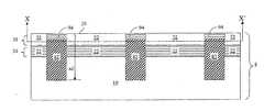
- a vertical cross-sectional view of a first exemplary semiconductor structurewhich comprises a semiconductor-on-insulator (SOI) substrate 8 containing a handle substrate 10 , a buried insulator layer 20 , and a top semiconductor layer 30 .
- the handle substrate 10may comprise a semiconductor material such as silicon.
- the handle substrate 10comprises a single crystalline semiconductor material.
- the handle substrate 10may have a p-type doping or an n-type doping.
- the conductivity of the doping of the handle substrate 10is herein referred to as a first conductivity type.
- the dopant concentration of the handle substrate 10is from about 1.0 ⁇ 10 14 /cm 3 to about 3.0 ⁇ 10 17 /cm 3 , and typically at a dopant concentration from about 1.0 ⁇ 10 15 /cm 3 to about 3.0 ⁇ 10 16 /cm 3 .
- the buried insulator layer 20comprises a dielectric material such as a silicon oxide or a silicon nitride. Preferably, the buried insulator layer 20 comprises thermal silicon oxide.
- the thickness of the buried insulator layer 20may be from about 50 nm to about 400 nm, and typically from about 100 nm to about 200 nm. Implementation of the present invention on a hybrid substrate containing a bulk portion and an SOI portion is explicitly contemplated herein.
- the top semiconductor layer 30comprises a semiconductor material that may be selected from, but is not limited to, silicon, germanium, silicon-germanium alloy, silicon carbon alloy, silicon-germanium-carbon alloy, gallium arsenide, indium arsenide, indium phosphide, III-V compound semiconductor materials, II-VI compound semiconductor materials, organic semiconductor materials, and other compound semiconductor materials.
- the thickness of the top semiconductor layer 30may be from about 5 nm to about 300 nm, and preferably from about 5 nm to about 100 nm.
- the entirety of the top semiconductor layer 30comprises a single crystalline semiconductor material.
- the top semiconductor layer 30may have a built-in biaxial stress in the plane of the top semiconductor layer 30 , i.e., in the plane perpendicular to the direction of the surface normal of a substrate top surface 29 , which is a top surface of the SOI substrate 8 .
- the top semiconductor layer 30may be substantially undoped of may have a doping of the first conductivity type or a doping of the opposite type of the first conductivity type, which is herein referred to as a second conductivity type.
- the dopant concentration of the top semiconductor layer 30may be from about 1.0 ⁇ 10 14 /cm 3 to about 3.0 ⁇ 10 17 /cm 3 , and typically from about 1.0 ⁇ 10 15 /cm 3 to about 3.0 ⁇ 10 16 /cm 3 , although lesser and greater dopant concentrations are explicitly contemplated herein.
- a stack of pad layersis formed on the substrate top surface 29 .
- a first pad oxide layer 40is formed directly on the substrate top surface.
- the first pad oxide layer 40may comprise a thermal oxide of the semiconductor material in the top semiconductor layer 30 , or may comprise a dielectric oxide material deposited by chemical vapor deposition (CVD).
- the first pad oxide layer 30may comprise a silicon oxide such as a thermal silicon oxide or a deposited silicon oxide formed by CVD.
- the thickness of the first pad layer 40is from about 3 nm to about 30 nm, and typically from about 5 nm to about 15 nm.
- a pad nitride layer 50is deposited on the first pad layer 40 , for example, by chemical vapor deposition such as low pressure chemical vapor deposition (LPCVD) or rapid thermal chemical vapor deposition (RTCVD).
- the pad nitride layer 50may comprise silicon nitride, or other dielectric nitride having sufficient resistance to chemical mechanical polishing.
- the thickness of the pad nitride layer 50may be from about 50 nm to about 250 nm, and typically from about 10 nm to about 20 nm.
- a second pad layer 50is formed on the pad nitride layer 50 , for example, by chemical vapor deposition such as low pressure chemical vapor deposition (LPCVD), rapid thermal chemical vapor deposition (RTCVD), or high density plasma chemical vapor deposition (HDPCVD).
- the second pad layer 50may comprise silicon oxide or other semiconductor oxide providing sufficient resistance to etching during a subsequent etching of silicon nitride.
- the thickness of the second pad oxide layer 60may be from about 10 nm to about 1,000 nm.
- the thickness of the second oxide layer 60depends on a target depth of a trench into the SOI substrate 8 and the nature of etching process employed to form the trench. For example, in case the depth of the trench to be formed, as measured from the substrate top surface to a bottom of the trench, is from about 200 nm to about 500 nm, and a soft mask process, in which the photoresist 71 is present throughout the etching process, the thickness of the second pad oxide layer may be from about 10 nm to about 100 nm.
- the thickness of the second pad oxide layermay be from about 50 nm to about 1,000 nm.
- FIG. 3is a vertical cross-sectional view and
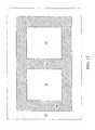
- FIG. 4is a top down view of the first exemplary semiconductor structure.
- the active areas AAcorrespond to areas in which the photoresist 71 remains after patterning.
- each of the active areas AAis disjoined from other active areas, i.e., an area devoid of the photoresist 71 encloses each of the active areas AA.
- the complement of the set of all active areas AAi.e., the area without the photoresist 71 , may be a single contiguous area, or may be multiple disjoined areas.
- a reactive ion etchis employed to transfer the pattern in the photoresist 71 into the stack of the second pad oxide layer 70 , the pad nitride layer 50 , and the first pad oxide layer 40 , exposing the substrate top surface 29 between the active areas AA.
- the photoresist 71may, or may not, be removed at this point depending on the depth of the trench to be subsequently formed and the etch chemistry to be employed therein.
- the pattern in the photoresist 71 or in the second pad oxide layer 70is transferred into the SOI substrate 8 by a reactive ion etch to a trench depth td from the substrate top surface 29 into the SOI substrate 8 .
- the trench depth tdis greater than the depth of a bottom surface of the buried insulator layer 20 as measured from the substrate top surface 29 .
- the trench depth dmay be from about 200 nm to about 8,000 nm.
- a single trench Tis formed.
- a plurality of disjoined trenchesis formed. Construction of a plurality of disjoined trenches requires modification of the pattern in the photoresist 71 , which is known to one of ordinary skill in the art.
- At least one top semiconductor portion 32 enclosed by the trench Tis formed from remaining portions of the top semiconductor layer 30 .
- the collection of all of the at least one top semiconductor portion 32constitutes the top semiconductor layer 30 .
- At least one buried insulator portion 22 enclosed by the trench Tis formed from remaining portions of the buried insulator layer 20 .
- the collection of all of the at least one buried insulator layer 22constitutes the buried insulator layer 20 .
- Each of the at least one top semiconductor portion 32vertically abuts one of the at least one buried insulator portion 22 .
- the sidewalls of each of the at least one top semiconductor portion 32 and sidewalls of the buried insulator portion 22 directly underneathare vertically coincident, i.e., coincident in a vertical view such as a top-down view.
- a silicon nitride layer 80is deposited in the trench T (See FIG. 5 ) and on the second pad oxide layer 70 .
- the trench Tis filled with the silicon nitride layer 80 .
- the silicon nitride layer 80comprises a stress-generating silicon nitride, which may be the same material as stress-generating silicon nitride liners formed over a gate electrode as known in the art.
- stress-generating silicon nitride liners of the prior arthaving a typical thickness from about 30 nm to about 80 nm, are known to generate compressive stress or tensile stress, of which the magnitude may exceed 0.2 GPa.
- the difference between the prior art and the present inventionis that such stress-generating silicon nitride is formed above a top surface of a semiconductor substrate over a gate electrode in the prior art, while the stress-generating silicon nitride is located in a trench formed beneath the substrate top surface 29 prior to formation of any gate electrode.
- the stress-generating silicon nitridemay be a tensile stress-generating silicon nitride or a compressive stress-generating silicon nitride.
- the portion of the silicon nitride layer 80 within the trench Texerts a compressive stress or a tensile stress to structures that the trench T encloses, which include the at least one top semiconductor portion 32 , the at least one buried insulator portion 22 , and the portion of the handle substrate 10 between a bottom surface of the buried insulator layer 20 and a bottom surface of the trench T.
- the magnitude of the compressive stress or the tensile stressmay be greater than 0.2 GPa in a region of each of the at least one top semiconductor portion 32 .
- the region in which the magnitude of the compressive stress or the tensile stress exceeds 0.2 GPamay include most of each of the at least one top semiconductor potion 32 except for a boundary region of each of the at least one top semiconductor portion 32 directly on the trench T.
- the thickness of the silicon nitride layer 80is greater than half of the narrowest distance in the opening of the trench T to insure complete fill of the trench. Consequently, the thickness of the silicon nitride layer is greater than half of the critical dimension, i.e., the minimum dimension that lithographic tools may print. The critical dimension is reduced with each generation of lithographic tools, and is about 50 nm as of 2007.
- the thickness of the silicon nitride layer 80may be from about 25 nm to about 300 nm, and preferably from about 25 nm to about 150 nm, although lesser and greater thicknesses are also explicitly contemplated herein.
- the stress-generating silicon nitride employed for the silicon nitride layer 80may be formed by chemical vapor deposition (CVD) such as plasma enhanced chemical vapor deposition (PECVD), high density plasma chemical vapor deposition (HDPCVD), rapid thermal chemical vapor deposition (RTCVD), low pressure chemical vapor deposition (LPCVD), or a combination thereof.
- CVDchemical vapor deposition
- PECVDplasma enhanced chemical vapor deposition
- HDPCVDhigh density plasma chemical vapor deposition
- RTCVDrapid thermal chemical vapor deposition
- LPCVDlow pressure chemical vapor deposition
- the silicon nitride layer 80(See FIG. 6 ) is recessed below a top surface of the at least one top semiconductor portion 32 .
- the depth of recess as measured from the top surface of the at least one top semiconductor portion 32which is herein referred to as a nitride recess depth nrd, may be less than the thickness of the at least one top semiconductor portion 32 so that the top surface of an insulator stressor plug 82 , which is the remaining portion of the silicon nitride layer 80 , is located between the top surface of the at least one top semiconductor portion 32 and a bottom surface of the at least one top semiconductor portion 32 .
- the nitride recess depth nrdmay be equal to the thickness of the at least one top semiconductor portion 32 so that the top surface of the insulator stressor plug 82 is at the depth of the bottom surface of the at least one top semiconductor portion 32 .
- the nitride recess depth nrdmay be greater than the thickness of the at least one top semiconductor portion 32 and less than the sum of the thickness of the at least one top semiconductor portion 32 and the thickness of the at least one buried insulator portion 22 so that the top surface of an insulator stressor plug 82 is located between a top surface of the at least one buried insulator portion 22 and a bottom surface of the at least one buried insulator portion 22 .
- the nitride recess depth nrdmay be equal to the sum of the thickness of the at least one top semiconductor portion 32 and the thickness of the at least one buried insulator portion 22 so that the top surface of the insulator stressor plug 82 is at the depth of the bottom surface of the at least one buried insulator portion 22 . Still alternately, the nitride recess depth nrd may be greater than the sum of the thickness of the at least one top semiconductor portion 32 and the thickness of the at least one buried insulator portion 22 so that the top surface of an insulator stressor plug 82 is located beneath the bottom surface of the at least one buried insulator portion 22 .
- etch processthat etches the silicon nitride layer 80 selective to the second pad oxide layer 70 is employed.
- the etch processis a reactive ion etch (RIE) process in which the etch ratio between the silicon nitride layer 80 and the second pad oxide layer 70 is high, so that at least a portion of the second pad oxide layer 70 remains at the end of the reactive ion etch.
- RIEreactive ion etch
- a silicon oxide layer 90is deposited on the insulator stressor plug 82 in the trench T (See FIG. 5 ) and on the second pad oxide layer 70 .
- the portion of the trench T above the insulator stressor plug 82is filled with the silicon oxide layer 90 .
- the silicon oxide layer 90may be formed by chemical vapor deposition (CVD) such as plasma enhanced chemical vapor deposition (PECVD), high density plasma chemical vapor deposition (HDPCVD), rapid thermal chemical vapor deposition (RTCVD), low pressure chemical vapor deposition (LPCVD), or a combination thereof.
- CVDchemical vapor deposition
- PECVDplasma enhanced chemical vapor deposition
- HDPCVDhigh density plasma chemical vapor deposition
- RTCVDrapid thermal chemical vapor deposition
- LPCVDlow pressure chemical vapor deposition
- a precursor containing silicon and oxygensuch as tetra-ethyl-ortho-silicate (TEOS) may be employed in the CVD process.
- TEOStetra-ethyl-ortho-silicate
- the silicon oxide layer 90may, or may not, comprise the same material as the second pad oxide layer 70 .
- the thickness of the silicon oxide layer 90is greater than half of the narrowest distance in the opening of the trench T to insure complete fill of the trench without a void. Consequently, the thickness of the silicon nitride layer is greater than half of the critical dimension.
- the thickness of the silicon oxide layer 90may be from about 25 nm to about 300 nm, and preferably from about 25 nm to about 150 nm, although lesser and greater thicknesses are also explicitly contemplated herein.
- the silicon oxide layer 90is planarized by chemical mechanical polishing (CMP) employing the pad nitride layer 50 as a stopping layer.
- CMPchemical mechanical polishing
- a recess etchwhich may be a reactive ion etch, a wet etch, a chemical downstream etch, or any combination thereof, may be employed in conjunction with the chemical mechanical polishing.
- Methods of performing a CMP process on a silicon oxide layer employing a nitride layer as the stopping layerare well known in the art.
- the remaining portion of the silicon oxide layer 90 after the CMP stepconstitutes a planarized silicon oxide layer 92 .
- a top surface of the planarized silicon oxide layer 92is substantially coplanar with a top surface of the pad nitride layer 50 .
- the planarized silicon oxide layer 92is recessed by a first etch that etches the planarized silicon oxide layer 92 selective to the pad nitride layer 50 .
- the first etchmay be a wet etch, a reactive ion etch, a chemical dry etch, or any combination thereof.
- An exemplary wet etch processis a wet etch employing hydrofluoric acid (HF), which selectively etches the planarized silicon oxide layer 92 relative to the pad nitride layer 50 .
- HFhydrofluoric acid
- the remaining portion of the planarized silicon oxide layer 92 after the etchconstitutes a silicon oxide plug 94 .
- a top surface of the silicon oxide plug 94is located about the interface between the first pad oxide layer 40 and the pad nitride layer 50 .
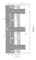
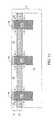
- FIG. 11is a vertical cross-sectional view of the first exemplary semiconductor structure.
- FIG. 12is a top-down view of the first exemplary semiconductor structure in FIG. 11 .
- FIG. 13is a horizontal cross-sectional view of the first exemplary semiconductor structure in FIG. 11 along the plane X-X′.
- the pad nitride layer 50is removed selective to the silicon oxide plug 94 and the first pad oxide layer 40 by a second etch, which may be a wet etch, a reactive ion etch, a chemical dry etch, or any combination thereof.
- a wet etch employing hot phosphoric acidmay be employed to selectively remove the pad nitride layer 50 , while not affecting the silicon oxide plug 94 and the first pad oxide layer 40 .
- the first pad oxide layer 40 and a top portion of the silicon oxide plug 94may then be removed by a third etch selective to the at least one top semiconductor portion 32 .
- the third etchmay be, for example, a wet etch employing hydrofluoric acid (HF).
- amount of removal of the top portion of the silicon oxide plug 92is such that a top surface of the silicon oxide plug 94 is substantially coplanar with the top surface of the at least one top semiconductor portion 32 .
- the first exemplary semiconductor structure of FIGS. 11-13comprises:
- a semiconductor-on-insulator (SOI) substrate 8including a handle substrate 10 , at least one buried insulator portion 22 abutting the handle substrate 10 , and at least one top semiconductor portion 32 abutting the at least one buried insulator portion 22 ;
- SOIsemiconductor-on-insulator
- a trenchextending from a top surface, which is the substrate top surface 29 , of the at least one top semiconductor portion 32 , to a depth s which is the trench depth td, below a bottom surface of the at least one buried insulator portion 22 ;
- an interface between the insulator stressor plug 82 and the silicon oxide plug 94is located between the top surface, which is the substrate top surface 29 , of the at least one top semiconductor portion 32 and a bottom surface of the at least one top semiconductor portion 32 .
- the first exemplary semiconductor structureprovides a substantially flat top surface, which is the substrate top surface 29 , over the entirety of the SOI substrate 8 . Further, the substrate top surface 29 comprises a semiconductor material of the at least one semiconductor portion 32 and silicon oxide of the silicon oxide plug 94 .
- This compositionis identical to the composition of a top surface of a conventional complementary metal-oxide-semiconductor (CMOS) structure after formation of shallow trench isolation.
- CMOScomplementary metal-oxide-semiconductor
- the first exemplary semiconductor structuremay employ identical processing steps after the processing step of FIGS. 11-13 as conventional CMOS structures. In other words, the first exemplary semiconductor structure is compatible with conventional semiconductor processing sequence after the step of FIGS. 11-13 .
- a stress schematic indicating the direction of stress generated by the insulator stressor plug 82is shown in superposition on the first exemplary semiconductor structure of FIG. 11 for the case in which the insulator stressor plug 82 generates a tensile stress.
- the tensile stressis applied to the handle substrate 10 and to the at least one top semiconductor portion 32 .
- a semiconductor devicemay be formed in the at least one top semiconductor portion 32 such that the tensile stress applied to the at least one top semiconductor portion 32 is advantageously utilized to enhance performance of the semiconductor device.
- the at least one top semiconductor portion 32may comprise silicon and the semiconductor device may be an n-type field effect transistor having a channel in the direction of the lateral tensile stress and employing electrons as charge carriers. In this case, the mobility of the electrons increases as a result of the lateral tensile stress on the at least one top semiconductor layer 32 .
- a stress schematic indicating the direction of stress generated by the insulator stressor plug 82is shown in superposition on the first exemplary semiconductor structure of FIG. 11 for the case in which the insulator stressor plug 82 generates a compressive stress.
- the compressive stressis applied to the handle substrate 10 and to the at least one top semiconductor portion 32 .
- a semiconductor devicemay be formed in the at least one top semiconductor portion 32 such that the compressive stress applied to the at least one top semiconductor portion 32 is advantageously utilized to enhance performance of the semiconductor device.
- the at least one top semiconductor portion 32may comprise silicon and the semiconductor device may be an p-type field effect transistor having a channel in the direction of the lateral compressive stress and employing holes as charge carriers. In this case, the mobility of the holes increases as a result of the lateral compressive stress on the at least one top semiconductor layer 32 .
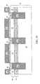
- FIG. 15a second exemplary semiconductor structure according to the present invention is shown.
- the interface between the insulator stressor plug 82 and the silicon oxide plug 94is located between a top surface, which is the substrate top surface 29 , of the at least one buried insulator portion 32 and the bottom surface of the at least one buried insulator portion 32 .
- FIG. 16a third exemplary semiconductor structure according to the present invention is shown.
- the interface between the insulator stressor plug 82 and the silicon oxide plug 94is located beneath the bottom surface of the at least one buried insulator portion 22 .
- Embodiments in which the interface between the insulator stressor plug 82 and the silicon oxide plug 94 is located at the bottom surface of the at least one top semiconductor portion 32 or at the bottom surface of the at least one buried insulator portion 22are explicitly contemplated herein.
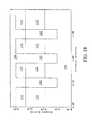
- FIG. 18a two-dimensional model for simulation of stress in a fourth exemplary semiconductor structure according to the present invention.
- the structure of the fourth exemplary semiconductor in the direction perpendicular to the plane of the model, i.e., the plane of FIG. 18is assumed to continue indefinitely, i.e., sufficiently long enough not to affect the results of the simulation.
- the cross-sectional area of a handle substrate 10(See FIG. 11 ) is approximated by a handle substrate area 110 .
- the cross-sectional area of an insulator stressor plug 82(See FIG. 11 ) is approximated by an insulator stressor plug area 182 .
- the cross-sectional area of at least one buried insulator portion 22(See FIG. 11 ) is approximated by at least one buried insulator portion area 122 .
- the cross-sectional area of at least one top semiconductor portion 32(See FIG. 11 ) is approximated by at least one top semiconductor portion area 132 .
- the effect of a silicon oxide plug 94is assumed to be insignificant, and a void area 199 was introduced in the area of the silicon oxide plug 94 .
- a top surface of the insulator stressor plug area 182is located at the bottom surface of the at least one top semiconductor portion area 132 .
- the insulator stressor plug area 182is assumed to have the same property as one of tensile silicon nitride material known in the art.
- FIG. 19is a plot of lateral stress from a simulation employing the two-dimensional model of FIG. 15 .
- Lateral tensile stress up to about 1.8 GPais observed in the at least one top semiconductor portion area 132 .
- the lateral tensile stressis greater than 0.5 GPa.
- the magnitude of the lateral tensile stressfalls below 0.5 GPa only near the boundary with the insulator stressor plug area 182 (See FIG. 18 ).
- the magnitude of the tensile stressmay be greater than 0.5 GPa in a region in the at least one top semiconductor portion 32 in the exemplary semiconductor structures demonstrated above.
Landscapes
- Engineering & Computer Science (AREA)
- Physics & Mathematics (AREA)
- Condensed Matter Physics & Semiconductors (AREA)
- General Physics & Mathematics (AREA)
- Manufacturing & Machinery (AREA)
- Computer Hardware Design (AREA)
- Microelectronics & Electronic Packaging (AREA)
- Power Engineering (AREA)
- Element Separation (AREA)
Abstract
Description
- This application is a divisional application of U.S. Ser. No. 13/370,898 filed on Feb. 10, 2012 which is a divisional application of U.S. Ser. No. 11/860,851, filed on Sep. 25, 2007. The entire contents of each of the aforementioned U.S. application are incorporated herein by reference.
- The present invention generally relates to semiconductor structures, and particularly to stress-generating structures for semiconductor-on-insulator (SOI) devices and methods of manufacturing the same.
- When stress is applied to the channel within an active area of a semiconductor transistor, the mobility of carriers, and as a consequence, the transconductance and the on-current of the transistor are altered from their corresponding values for a transistor containing an unstressed semiconductor. This is because the applied stress and the resulting strain on the semiconductor structure within the channel affects the band gap structure (i.e., breaks the degeneracy of the band structure) and changes the effective mass of carriers. The effect of the stress depends on the crystallographic orientation of the plane of the channel, the direction of the channel within the crystallographic orientation, the direction of the applied stress, and the type of carries.
- The effect of stress on the performance of semiconductor devices, especially on the performance of a metal-oxide-semiconductor field effect transistor (MOSFET, or a “FET” in short) device built on a silicon substrate, has been extensively studied in the semiconductor industry. For a p-type MOSFET (PMOSFET, or a “PFET” in short) utilizing a silicon channel, the mobility of minority carriers in the channel (which are holes in this case) increases under uniaxial compressive stress along the direction of the channel, i.e., the direction of the movement of holes or the direction connecting the drain to the source. Conversely, for an n-type MOSFET (NMOSFET, or an “NFET” in short) devices utilizing a silicon channel, the mobility of minority carriers in the channel (which are electrons in this case) increases under uniaxial tensile stress along the direction of the channel, i.e., the direction of the movement of electrons or the direction connecting the drain to the source. Tensile stress in transverse direction, i.e., the direction perpendicular to the movement of carries, can enhance both electron and hole mobilities. Thus, performance of field effect transistors may be improved by forming a stress-generating structure in or on a semiconductor substrate.
- Methods of employing stress-generating shallow trench isolation liners in a bulk substrate are known in the art. Direct application of such methods to semiconductor-on-insulator substrate results in an insignificant amount of improvement in performance compared to bulk equivalents. This is because the thickness of a top semiconductor layer is much less than a depth of shallow trench isolation in bulk substrates, which may be from about 300 nm to about 450 nm, and the amount of stress transferred to SOI devices is proportional to the thickness of the top semiconductor layer, which may be from about 5 nm to about 30 nm in the case of ultra-thin semiconductor-on-insulator (UTSOI) substrates employed for high performance devices.
- In view of the above, there exists a need for an effective stress-generating structure for semiconductor-on-insulator (SOI) devices, and methods of manufacturing the same.
- Further, current semiconductor processing sequence used in industry employs silicon oxide as a trench fill material. Modification of an exposed structure of the trench isolation structure would require alterations to subsequent processing steps.
- Therefore, there exists a need for an effective stress-generating structure that is compatible with existing semiconductor processing after formation of trench isolation structures, and methods of manufacturing the same.
- The present invention addresses the needs described above by providing a stress-generating structure which is compatible with semiconductor-on-insulator substrates and existing processing after formation of trench isolation structures, and methods of manufacturing the same.
- In the present invention, a stack of pad layers including a first pad oxide layer, a pad nitride layer, and a second pad oxide layer are formed on a semiconductor-on-insulator (SOI) substrate. A deep trench extending below a bottom surface of a buried insulator layer of the SOI substrate and enclosing at least one top semiconductor region is formed by lithographic methods and etching. A stress-generating nitride material is deposited in the deep trench and recessed below a top surface of the SOI substrate to form a stress-generating buried nitride plug in the deep trench. A silicon oxide material is deposited in the deep trench, planarized, and recessed. The stack of pad layers is removed to expose substantially coplanar top surfaces of the top semiconductor layer and of silicon oxide plugs. The stress-generating buried nitride plug encloses, and generates either a compressive stress or tensile stress to, the at least one top semiconductor region.
- According to an aspect of the present invention, a semiconductor structure is provided which comprises:
- a semiconductor-on-insulator (SOI) substrate including a handle substrate, at least one buried insulator portion abutting the handle substrate, and at least one top semiconductor portion abutting the at least one buried insulator portion;
- a trench extending from a top surface of the at least one top semiconductor portion to a depth below a top surface of the at least one buried insulator portion; and
- a stack of an insulator stressor plug and a silicon oxide plug located in the trench, wherein the insulator stressor plug abuts a bottom surface of the trench and the silicon oxide plug is substantially coplanar with the top surface of the at least one top semiconductor portion.
- In one embodiment, the trench extends a depth below a bottom surface of the at least one buried insulator portion.
- In another embodiment, the insulator stressor plug comprises a silicon nitride and applies a tensile stress or a compressive stress to the at least one top semiconductor portion.
- In even another embodiment, a magnitude of the tensile stress or the compressive stress is greater than 0.2 GPa in a region in the at least one top semiconductor portion.
- In yet another embodiment, the insulator stressor plug laterally abuts, and encloses, the at least one buried insulator portion.
- In still another embodiment, the insulator stressor plug laterally abuts and encloses the at least one top semiconductor portion.
- In still yet another embodiment, an interface between the insulator stressor plug and the silicon oxide plug is located between the top surface of the at least one top semiconductor portion and a bottom surface of the at least one top semiconductor portion, or at the bottom surface of the at least one top semiconductor portion.
- In a further embodiment, an interface between the insulator stressor plug and the silicon oxide plug is located between a top surface of the at least one buried insulator portion and the bottom surface of the at least one buried insulator portion, or at the bottom surface of the at least one buried insulator portion.
- In an even further embodiment, an interface between the insulator stressor plug and the silicon oxide plug is located beneath the bottom surface of the at least one buried insulator portion.
- In a yet further embodiment, the at least one top semiconductor layer comprises one of silicon, germanium, a silicon germanium alloy, a silicon carbon alloy, and a silicon germanium carbon alloy.
- In a still further embodiment, a thickness of the at least one top semiconductor portion is from about 5 nm to about 300 nm, and wherein a depth of the trench is from about 200 nm to about 8,000 nm.
- According to another aspect of the present invention, a method of forming a semiconductor structure is provided, which comprises:
- forming a trench extending from a top surface of a semiconductor-on-insulator (SOI) substrate to a depth beneath a bottom surface of a buried insulator layer of the SOI substrate; and
- forming a stack of an insulator stressor plug and a silicon oxide plug in the trench, wherein the insulator stressor plug abuts a bottom surface of the trench, and wherein the silicon oxide plug is substantially coplanar with a top surface of at least one top semiconductor portion formed in a top semiconductor layer of the SOI substrate.
- In one embodiment, the method further comprises:
- forming a stack of pad layers directly on the SOI substrate; applying a photoresist on the stack of pad layers and lithographically patterning the photoresist; and
- transferring a pattern in the resist into the stack of pad layers and the SOI substrate by at least one reactive etch.
- In another embodiment, the trench laterally abuts and encloses the at least one top semiconductor portion and at least one buried insulator portion, wherein the at least one buried insulator portion vertically abuts the at least one top semiconductor portion.
- In yet another embodiment, the method further comprises:
- depositing a silicon nitride into the trench; and
- recessing the silicon nitride in the trench to form the insulator stressor plug.
- In still another embodiment, the insulator stressor plug comprises a silicon nitride and applies a compressive stress or a tensile stress to the at least one top semiconductor portion.
- In still yet another embodiment, a magnitude of the tensile stress or the compressive stress exceeds 0.2 GPa in a region in the at least one top semiconductor portion.
- In a further embodiment, the method further comprises:
- depositing a silicon oxide into the trench on top of the insulator stressor plug; and
- recessing the silicon oxide in the trench to form the silicon oxide plug.
- In an even further embodiment, an interface between the insulator stressor plug and the silicon oxide plug is located between the top surface of the at least one top semiconductor portion and a bottom surface of the at least one top semiconductor portion, or at the bottom surface of the at least one top semiconductor portion.
- In a yet further embodiment, an interface between the insulator stressor plug and the silicon oxide plug is located between a top surface of the buried insulator layer and the bottom surface of the buried insulator layer, or at the bottom surface of the buried insulator layer.
- In a still further embodiment, a thickness of the at least one top semiconductor portion is from about 5 nm to about 300 nm, and wherein a depth of the trench is from about 200 nm to about 8,000 nm.
FIGS. 1-3 ,5-11 are sequential vertical cross-sectional views of a first exemplary semiconductor structure according to the present invention.FIG. 4 is a top-down view of the exemplary semiconductor structure inFIG. 4 .FIG. 12 is a top-down view of the exemplary semiconductor structure inFIG. 11 .FIG. 13 is a horizontal cross-sectional view of the exemplary semiconductor structure inFIG. 11 along the plane X-X′.- Each of
FIGS. 14-15 is a superposition ofFIG. 11 with a stress schematic indicating the direction of stress generated by a stress-generating nitride plug. FIG. 16 is a vertical cross-sectional view of a second exemplary semiconductor structure according to the present invention.FIG. 17 is a vertical cross-sectional view of a third exemplary semiconductor structure according to the present invention.FIG. 18 is a two-dimensional model for simulation of stress in a fourth exemplary semiconductor structure according to the present invention.FIG. 19 is a plot of lateral stress from a simulation employing the two-dimensional model ofFIG. 15 .- As stated above, the present invention relates to particularly to stress-generating structures for semiconductor-on-insulator (SOI) devices and methods of manufacturing the same, which are now described in detail with accompanying figures. It is noted that like and corresponding elements are referred to by like reference numerals.
- Referring to
FIG. 1 , a vertical cross-sectional view of a first exemplary semiconductor structure is shown, which comprises a semiconductor-on-insulator (SOI)substrate 8 containing ahandle substrate 10, a buriedinsulator layer 20, and atop semiconductor layer 30. Thehandle substrate 10 may comprise a semiconductor material such as silicon. Preferably, thehandle substrate 10 comprises a single crystalline semiconductor material. Thehandle substrate 10 may have a p-type doping or an n-type doping. The conductivity of the doping of thehandle substrate 10 is herein referred to as a first conductivity type. The dopant concentration of thehandle substrate 10 is from about 1.0×10¹⁴/cm3to about 3.0×10¹⁷/cm3, and typically at a dopant concentration from about 1.0×10¹⁵/cm3to about 3.0×10¹⁶/cm3. The buriedinsulator layer 20 comprises a dielectric material such as a silicon oxide or a silicon nitride. Preferably, the buriedinsulator layer 20 comprises thermal silicon oxide. The thickness of the buriedinsulator layer 20 may be from about 50 nm to about 400 nm, and typically from about 100 nm to about 200 nm. Implementation of the present invention on a hybrid substrate containing a bulk portion and an SOI portion is explicitly contemplated herein. - The
top semiconductor layer 30 comprises a semiconductor material that may be selected from, but is not limited to, silicon, germanium, silicon-germanium alloy, silicon carbon alloy, silicon-germanium-carbon alloy, gallium arsenide, indium arsenide, indium phosphide, III-V compound semiconductor materials, II-VI compound semiconductor materials, organic semiconductor materials, and other compound semiconductor materials. The thickness of thetop semiconductor layer 30 may be from about 5 nm to about 300 nm, and preferably from about 5 nm to about 100 nm. Preferably, the entirety of thetop semiconductor layer 30 comprises a single crystalline semiconductor material. - The
top semiconductor layer 30 may have a built-in biaxial stress in the plane of thetop semiconductor layer 30, i.e., in the plane perpendicular to the direction of the surface normal of asubstrate top surface 29, which is a top surface of theSOI substrate 8. Thetop semiconductor layer 30 may be substantially undoped of may have a doping of the first conductivity type or a doping of the opposite type of the first conductivity type, which is herein referred to as a second conductivity type. The dopant concentration of thetop semiconductor layer 30 may be from about 1.0×10¹⁴/cm3to about 3.0×10¹⁷/cm3, and typically from about 1.0×10¹⁵/cm3to about 3.0×10¹⁶/cm3, although lesser and greater dopant concentrations are explicitly contemplated herein. - Referring to
FIG. 2 , a stack of pad layers is formed on thesubstrate top surface 29. Specifically, a firstpad oxide layer 40 is formed directly on the substrate top surface. The firstpad oxide layer 40 may comprise a thermal oxide of the semiconductor material in thetop semiconductor layer 30, or may comprise a dielectric oxide material deposited by chemical vapor deposition (CVD). The firstpad oxide layer 30 may comprise a silicon oxide such as a thermal silicon oxide or a deposited silicon oxide formed by CVD. The thickness of thefirst pad layer 40 is from about 3 nm to about 30 nm, and typically from about 5 nm to about 15 nm. - A
pad nitride layer 50 is deposited on thefirst pad layer 40, for example, by chemical vapor deposition such as low pressure chemical vapor deposition (LPCVD) or rapid thermal chemical vapor deposition (RTCVD). Thepad nitride layer 50 may comprise silicon nitride, or other dielectric nitride having sufficient resistance to chemical mechanical polishing. The thickness of thepad nitride layer 50 may be from about 50 nm to about 250 nm, and typically from about 10 nm to about 20 nm. - A
second pad layer 50 is formed on thepad nitride layer 50, for example, by chemical vapor deposition such as low pressure chemical vapor deposition (LPCVD), rapid thermal chemical vapor deposition (RTCVD), or high density plasma chemical vapor deposition (HDPCVD). Thesecond pad layer 50 may comprise silicon oxide or other semiconductor oxide providing sufficient resistance to etching during a subsequent etching of silicon nitride. - The thickness of the second
pad oxide layer 60 may be from about 10 nm to about 1,000 nm. The thickness of thesecond oxide layer 60 depends on a target depth of a trench into theSOI substrate 8 and the nature of etching process employed to form the trench. For example, in case the depth of the trench to be formed, as measured from the substrate top surface to a bottom of the trench, is from about 200 nm to about 500 nm, and a soft mask process, in which thephotoresist 71 is present throughout the etching process, the thickness of the second pad oxide layer may be from about 10 nm to about 100 nm. In case the depth of the trench to be formed is from about 500 nm to about 8,000 nm, and a hard mask process, in which thephotoresist 71 is consumed or removed during the etching process and the secondpad oxide layer 60 as patterned is employed as an etch mask, the thickness of the second pad oxide layer may be from about 50 nm to about 1,000 nm. - Referring to
FIGS. 3 and 4 , aphotoresist 71 is applied onto the top surface of the second pad layer and is lithographically patterned to define active areas AA, within which semiconductor devices are subsequently formed.FIG. 3 is a vertical cross-sectional view and FIG. 4 is a top down view of the first exemplary semiconductor structure. The active areas AA correspond to areas in which thephotoresist 71 remains after patterning. Typically, each of the active areas AA is disjoined from other active areas, i.e., an area devoid of thephotoresist 71 encloses each of the active areas AA. The complement of the set of all active areas AA, i.e., the area without thephotoresist 71, may be a single contiguous area, or may be multiple disjoined areas.- A reactive ion etch is employed to transfer the pattern in the
photoresist 71 into the stack of the secondpad oxide layer 70, thepad nitride layer 50, and the firstpad oxide layer 40, exposing thesubstrate top surface 29 between the active areas AA. Thephotoresist 71 may, or may not, be removed at this point depending on the depth of the trench to be subsequently formed and the etch chemistry to be employed therein. - Referring to
FIG. 5 , the pattern in thephotoresist 71 or in the secondpad oxide layer 70 is transferred into theSOI substrate 8 by a reactive ion etch to a trench depth td from thesubstrate top surface 29 into theSOI substrate 8. The trench depth td is greater than the depth of a bottom surface of the buriedinsulator layer 20 as measured from thesubstrate top surface 29. The trench depth d may be from about 200 nm to about 8,000 nm. In case the complement of the set of all active areas AA is a single contiguous area, a single trench T is formed. In case the complement of the set of all active areas AA comprises multiple disjoined areas, a plurality of disjoined trenches is formed. Construction of a plurality of disjoined trenches requires modification of the pattern in thephotoresist 71, which is known to one of ordinary skill in the art. - At least one
top semiconductor portion 32 enclosed by the trench T is formed from remaining portions of thetop semiconductor layer 30. The collection of all of the at least onetop semiconductor portion 32 constitutes thetop semiconductor layer 30. At least one buriedinsulator portion 22 enclosed by the trench T is formed from remaining portions of the buriedinsulator layer 20. The collection of all of the at least one buriedinsulator layer 22 constitutes the buriedinsulator layer 20. Each of the at least onetop semiconductor portion 32 vertically abuts one of the at least one buriedinsulator portion 22. The sidewalls of each of the at least onetop semiconductor portion 32 and sidewalls of the buriedinsulator portion 22 directly underneath are vertically coincident, i.e., coincident in a vertical view such as a top-down view. - Referring to
FIG. 6 , a silicon nitride layer80 is deposited in the trench T (SeeFIG. 5 ) and on the secondpad oxide layer 70. The trench T is filled with the silicon nitride layer80. Preferably, the silicon nitride layer80 comprises a stress-generating silicon nitride, which may be the same material as stress-generating silicon nitride liners formed over a gate electrode as known in the art. Such stress-generating silicon nitride liners of the prior art, having a typical thickness from about 30 nm to about 80 nm, are known to generate compressive stress or tensile stress, of which the magnitude may exceed 0.2 GPa. The difference between the prior art and the present invention is that such stress-generating silicon nitride is formed above a top surface of a semiconductor substrate over a gate electrode in the prior art, while the stress-generating silicon nitride is located in a trench formed beneath thesubstrate top surface 29 prior to formation of any gate electrode. - As such, the stress-generating silicon nitride may be a tensile stress-generating silicon nitride or a compressive stress-generating silicon nitride. The portion of the silicon nitride layer80 within the trench T exerts a compressive stress or a tensile stress to structures that the trench T encloses, which include the at least one
top semiconductor portion 32, the at least one buriedinsulator portion 22, and the portion of thehandle substrate 10 between a bottom surface of the buriedinsulator layer 20 and a bottom surface of the trench T. The magnitude of the compressive stress or the tensile stress may be greater than 0.2 GPa in a region of each of the at least onetop semiconductor portion 32. In practice, the region in which the magnitude of the compressive stress or the tensile stress exceeds 0.2 GPa may include most of each of the at least onetop semiconductor potion 32 except for a boundary region of each of the at least onetop semiconductor portion 32 directly on the trench T. - The thickness of the silicon nitride layer80, as measured above the second
pad oxide layer 70, is greater than half of the narrowest distance in the opening of the trench T to insure complete fill of the trench. Consequently, the thickness of the silicon nitride layer is greater than half of the critical dimension, i.e., the minimum dimension that lithographic tools may print. The critical dimension is reduced with each generation of lithographic tools, and is about 50 nm as of 2007. The thickness of the silicon nitride layer80 may be from about 25 nm to about 300 nm, and preferably from about 25 nm to about 150 nm, although lesser and greater thicknesses are also explicitly contemplated herein. - The stress-generating silicon nitride employed for the silicon nitride layer80 may be formed by chemical vapor deposition (CVD) such as plasma enhanced chemical vapor deposition (PECVD), high density plasma chemical vapor deposition (HDPCVD), rapid thermal chemical vapor deposition (RTCVD), low pressure chemical vapor deposition (LPCVD), or a combination thereof.
- Referring to
FIG. 7 , the silicon nitride layer80 (SeeFIG. 6 ) is recessed below a top surface of the at least onetop semiconductor portion 32. The depth of recess as measured from the top surface of the at least onetop semiconductor portion 32, which is herein referred to as a nitride recess depth nrd, may be less than the thickness of the at least onetop semiconductor portion 32 so that the top surface of aninsulator stressor plug 82, which is the remaining portion of the silicon nitride layer80, is located between the top surface of the at least onetop semiconductor portion 32 and a bottom surface of the at least onetop semiconductor portion 32. Alternately, the nitride recess depth nrd, may be equal to the thickness of the at least onetop semiconductor portion 32 so that the top surface of theinsulator stressor plug 82 is at the depth of the bottom surface of the at least onetop semiconductor portion 32. Even alternately, the nitride recess depth nrd may be greater than the thickness of the at least onetop semiconductor portion 32 and less than the sum of the thickness of the at least onetop semiconductor portion 32 and the thickness of the at least one buriedinsulator portion 22 so that the top surface of aninsulator stressor plug 82 is located between a top surface of the at least one buriedinsulator portion 22 and a bottom surface of the at least one buriedinsulator portion 22. Yet alternately, the nitride recess depth nrd, may be equal to the sum of the thickness of the at least onetop semiconductor portion 32 and the thickness of the at least one buriedinsulator portion 22 so that the top surface of theinsulator stressor plug 82 is at the depth of the bottom surface of the at least one buriedinsulator portion 22. Still alternately, the nitride recess depth nrd may be greater than the sum of the thickness of the at least onetop semiconductor portion 32 and the thickness of the at least one buriedinsulator portion 22 so that the top surface of aninsulator stressor plug 82 is located beneath the bottom surface of the at least one buriedinsulator portion 22. - An etch process that etches the silicon nitride layer80 selective to the second
pad oxide layer 70 is employed. Preferably, the etch process is a reactive ion etch (RIE) process in which the etch ratio between the silicon nitride layer80 and the secondpad oxide layer 70 is high, so that at least a portion of the secondpad oxide layer 70 remains at the end of the reactive ion etch. - Referring to
FIG. 8 , asilicon oxide layer 90 is deposited on the insulator stressor plug82 in the trench T (SeeFIG. 5 ) and on the secondpad oxide layer 70. The portion of the trench T above theinsulator stressor plug 82 is filled with thesilicon oxide layer 90. - The
silicon oxide layer 90 may be formed by chemical vapor deposition (CVD) such as plasma enhanced chemical vapor deposition (PECVD), high density plasma chemical vapor deposition (HDPCVD), rapid thermal chemical vapor deposition (RTCVD), low pressure chemical vapor deposition (LPCVD), or a combination thereof. A precursor containing silicon and oxygen, such as tetra-ethyl-ortho-silicate (TEOS) may be employed in the CVD process. Thesilicon oxide layer 90 may, or may not, comprise the same material as the secondpad oxide layer 70. - The thickness of the
silicon oxide layer 90, as measured above the secondpad oxide layer 70, is greater than half of the narrowest distance in the opening of the trench T to insure complete fill of the trench without a void. Consequently, the thickness of the silicon nitride layer is greater than half of the critical dimension. The thickness of thesilicon oxide layer 90 may be from about 25 nm to about 300 nm, and preferably from about 25 nm to about 150 nm, although lesser and greater thicknesses are also explicitly contemplated herein. - Referring to
FIG. 9 , thesilicon oxide layer 90 is planarized by chemical mechanical polishing (CMP) employing thepad nitride layer 50 as a stopping layer. Optionally, a recess etch, which may be a reactive ion etch, a wet etch, a chemical downstream etch, or any combination thereof, may be employed in conjunction with the chemical mechanical polishing. Methods of performing a CMP process on a silicon oxide layer employing a nitride layer as the stopping layer are well known in the art. The remaining portion of thesilicon oxide layer 90 after the CMP step constitutes a planarizedsilicon oxide layer 92. A top surface of the planarizedsilicon oxide layer 92 is substantially coplanar with a top surface of thepad nitride layer 50. - Referring to
FIG. 10 , the planarizedsilicon oxide layer 92 is recessed by a first etch that etches the planarizedsilicon oxide layer 92 selective to thepad nitride layer 50. The first etch may be a wet etch, a reactive ion etch, a chemical dry etch, or any combination thereof. An exemplary wet etch process is a wet etch employing hydrofluoric acid (HF), which selectively etches the planarizedsilicon oxide layer 92 relative to thepad nitride layer 50. The remaining portion of the planarizedsilicon oxide layer 92 after the etch constitutes asilicon oxide plug 94. Preferably, a top surface of the silicon oxide plug94 is located about the interface between the firstpad oxide layer 40 and thepad nitride layer 50. - Referring to
FIGS. 11-13 , thepad nitride layer 50, the firstpad oxide layer 40, and a top portion of the silicon oxide plug94 are removed.FIG. 11 is a vertical cross-sectional view of the first exemplary semiconductor structure.FIG. 12 is a top-down view of the first exemplary semiconductor structure inFIG. 11 .FIG. 13 is a horizontal cross-sectional view of the first exemplary semiconductor structure inFIG. 11 along the plane X-X′. - Specifically, the
pad nitride layer 50 is removed selective to thesilicon oxide plug 94 and the firstpad oxide layer 40 by a second etch, which may be a wet etch, a reactive ion etch, a chemical dry etch, or any combination thereof. In case thepad nitride layer 50 comprises silicon nitride, a wet etch employing hot phosphoric acid may be employed to selectively remove thepad nitride layer 50, while not affecting thesilicon oxide plug 94 and the firstpad oxide layer 40. - The first
pad oxide layer 40 and a top portion of the silicon oxide plug94 may then be removed by a third etch selective to the at least onetop semiconductor portion 32. The third etch may be, for example, a wet etch employing hydrofluoric acid (HF). Preferably, amount of removal of the top portion of the silicon oxide plug92 is such that a top surface of the silicon oxide plug94 is substantially coplanar with the top surface of the at least onetop semiconductor portion 32. - The first exemplary semiconductor structure of
FIGS. 11-13 comprises: - a semiconductor-on-insulator (SOI)
substrate 8 including ahandle substrate 10, at least one buriedinsulator portion 22 abutting thehandle substrate 10, and at least onetop semiconductor portion 32 abutting the at least one buriedinsulator portion 22; - a trench extending from a top surface, which is the
substrate top surface 29, of the at least onetop semiconductor portion 32, to a depthswhich is the trench depth td, below a bottom surface of the at least one buriedinsulator portion 22; and - a stack of an
insulator stressor plug 82 and a silicon oxide plug94 located in the trench, wherein theinsulator stressor plug 82 abuts a bottom surface of the trench and the silicon oxide plug94 is substantially coplanar with the top surface, which is thesubstrate top surface 29, of the at least onetop semiconductor portion 32. - In the first exemplary semiconductor structure, an interface between the
insulator stressor plug 82 and the silicon oxide plug94 is located between the top surface, which is thesubstrate top surface 29, of the at least onetop semiconductor portion 32 and a bottom surface of the at least onetop semiconductor portion 32. - The first exemplary semiconductor structure provides a substantially flat top surface, which is the
substrate top surface 29, over the entirety of theSOI substrate 8. Further, thesubstrate top surface 29 comprises a semiconductor material of the at least onesemiconductor portion 32 and silicon oxide of thesilicon oxide plug 94. This composition is identical to the composition of a top surface of a conventional complementary metal-oxide-semiconductor (CMOS) structure after formation of shallow trench isolation. Thus, the first exemplary semiconductor structure may employ identical processing steps after the processing step ofFIGS. 11-13 as conventional CMOS structures. In other words, the first exemplary semiconductor structure is compatible with conventional semiconductor processing sequence after the step ofFIGS. 11-13 . - Referring to
FIG. 14 , a stress schematic indicating the direction of stress generated by theinsulator stressor plug 82 is shown in superposition on the first exemplary semiconductor structure ofFIG. 11 for the case in which theinsulator stressor plug 82 generates a tensile stress. The tensile stress is applied to thehandle substrate 10 and to the at least onetop semiconductor portion 32. A semiconductor device may be formed in the at least onetop semiconductor portion 32 such that the tensile stress applied to the at least onetop semiconductor portion 32 is advantageously utilized to enhance performance of the semiconductor device. For example, the at least onetop semiconductor portion 32 may comprise silicon and the semiconductor device may be an n-type field effect transistor having a channel in the direction of the lateral tensile stress and employing electrons as charge carriers. In this case, the mobility of the electrons increases as a result of the lateral tensile stress on the at least onetop semiconductor layer 32. - Referring to
FIG. 15 , a stress schematic indicating the direction of stress generated by theinsulator stressor plug 82 is shown in superposition on the first exemplary semiconductor structure ofFIG. 11 for the case in which theinsulator stressor plug 82 generates a compressive stress. The compressive stress is applied to thehandle substrate 10 and to the at least onetop semiconductor portion 32. A semiconductor device may be formed in the at least onetop semiconductor portion 32 such that the compressive stress applied to the at least onetop semiconductor portion 32 is advantageously utilized to enhance performance of the semiconductor device. For example, the at least onetop semiconductor portion 32 may comprise silicon and the semiconductor device may be an p-type field effect transistor having a channel in the direction of the lateral compressive stress and employing holes as charge carriers. In this case, the mobility of the holes increases as a result of the lateral compressive stress on the at least onetop semiconductor layer 32. - Referring to
FIG. 15 , a second exemplary semiconductor structure according to the present invention is shown. The interface between theinsulator stressor plug 82 and the silicon oxide plug94 is located between a top surface, which is thesubstrate top surface 29, of the at least one buriedinsulator portion 32 and the bottom surface of the at least one buriedinsulator portion 32. - Referring to
FIG. 16 , a third exemplary semiconductor structure according to the present invention is shown. The interface between theinsulator stressor plug 82 and the silicon oxide plug94 is located beneath the bottom surface of the at least one buriedinsulator portion 22. - Embodiments in which the interface between the
insulator stressor plug 82 and the silicon oxide plug94 is located at the bottom surface of the at least onetop semiconductor portion 32 or at the bottom surface of the at least one buriedinsulator portion 22 are explicitly contemplated herein. - Referring to
FIG. 18 , a two-dimensional model for simulation of stress in a fourth exemplary semiconductor structure according to the present invention. In this two-dimensional model, the structure of the fourth exemplary semiconductor in the direction perpendicular to the plane of the model, i.e., the plane ofFIG. 18 , is assumed to continue indefinitely, i.e., sufficiently long enough not to affect the results of the simulation. - The cross-sectional area of a handle substrate10 (See
FIG. 11 ) is approximated by ahandle substrate area 110. The cross-sectional area of an insulator stressor plug82 (SeeFIG. 11 ) is approximated by an insulatorstressor plug area 182. The cross-sectional area of at least one buried insulator portion22 (SeeFIG. 11 ) is approximated by at least one buriedinsulator portion area 122. The cross-sectional area of at least one top semiconductor portion32 (SeeFIG. 11 ) is approximated by at least one topsemiconductor portion area 132. The effect of a silicon oxide plug94 is assumed to be insignificant, and avoid area 199 was introduced in the area of thesilicon oxide plug 94. In this two-dimensional model, a top surface of the insulatorstressor plug area 182 is located at the bottom surface of the at least one topsemiconductor portion area 132. The insulatorstressor plug area 182 is assumed to have the same property as one of tensile silicon nitride material known in the art. FIG. 19 is a plot of lateral stress from a simulation employing the two-dimensional model ofFIG. 15 . Lateral tensile stress up to about 1.8 GPa is observed in the at least one topsemiconductor portion area 132. In most regions of the at least one topsemiconductor portion area 132, the lateral tensile stress is greater than 0.5 GPa. The magnitude of the lateral tensile stress falls below 0.5 GPa only near the boundary with the insulator stressor plug area182 (SeeFIG. 18 ). Thus, the magnitude of the tensile stress may be greater than 0.5 GPa in a region in the at least onetop semiconductor portion 32 in the exemplary semiconductor structures demonstrated above.- While the present invention has been particularly shown and described with respect to preferred embodiments thereof, it will be understood by those skilled in the art that the foregoing and other changes in forms and details may be made without departing from the spirit and scope of the present invention. It is therefore intended that the present invention not be limited to the exact forms and details described and illustrated, but fall within the scope of the appended claims.
Claims (20)
Priority Applications (1)
| Application Number | Priority Date | Filing Date | Title |
|---|---|---|---|
| US13/778,419US9305999B2 (en) | 2007-09-25 | 2013-02-27 | Stress-generating structure for semiconductor-on-insulator devices |
Applications Claiming Priority (3)
| Application Number | Priority Date | Filing Date | Title |
|---|---|---|---|
| US11/860,851US8115254B2 (en) | 2007-09-25 | 2007-09-25 | Semiconductor-on-insulator structures including a trench containing an insulator stressor plug and method of fabricating same |
| US13/370,898US8629501B2 (en) | 2007-09-25 | 2012-02-10 | Stress-generating structure for semiconductor-on-insulator devices |
| US13/778,419US9305999B2 (en) | 2007-09-25 | 2013-02-27 | Stress-generating structure for semiconductor-on-insulator devices |
Related Parent Applications (1)
| Application Number | Title | Priority Date | Filing Date |
|---|---|---|---|
| US13/370,898DivisionUS8629501B2 (en) | 2007-09-25 | 2012-02-10 | Stress-generating structure for semiconductor-on-insulator devices |
Publications (2)
| Publication Number | Publication Date |
|---|---|
| US20130168804A1true US20130168804A1 (en) | 2013-07-04 |
| US9305999B2 US9305999B2 (en) | 2016-04-05 |
Family
ID=40470735
Family Applications (3)
| Application Number | Title | Priority Date | Filing Date |
|---|---|---|---|
| US11/860,851Expired - Fee RelatedUS8115254B2 (en) | 2007-09-25 | 2007-09-25 | Semiconductor-on-insulator structures including a trench containing an insulator stressor plug and method of fabricating same |
| US13/370,898Active2027-10-01US8629501B2 (en) | 2007-09-25 | 2012-02-10 | Stress-generating structure for semiconductor-on-insulator devices |
| US13/778,419Active2028-01-06US9305999B2 (en) | 2007-09-25 | 2013-02-27 | Stress-generating structure for semiconductor-on-insulator devices |
Family Applications Before (2)
| Application Number | Title | Priority Date | Filing Date |
|---|---|---|---|
| US11/860,851Expired - Fee RelatedUS8115254B2 (en) | 2007-09-25 | 2007-09-25 | Semiconductor-on-insulator structures including a trench containing an insulator stressor plug and method of fabricating same |
| US13/370,898Active2027-10-01US8629501B2 (en) | 2007-09-25 | 2012-02-10 | Stress-generating structure for semiconductor-on-insulator devices |
Country Status (1)
| Country | Link |
|---|---|
| US (3) | US8115254B2 (en) |
Cited By (1)
| Publication number | Priority date | Publication date | Assignee | Title |
|---|---|---|---|---|
| US9362400B1 (en) | 2015-03-06 | 2016-06-07 | International Business Machines Corporation | Semiconductor device including dielectrically isolated finFETs and buried stressor |
Families Citing this family (11)
| Publication number | Priority date | Publication date | Assignee | Title |
|---|---|---|---|---|
| US8354675B2 (en) | 2010-05-07 | 2013-01-15 | International Business Machines Corporation | Enhanced capacitance deep trench capacitor for EDRAM |
| CN102280402A (en)* | 2010-06-12 | 2011-12-14 | 上海华虹Nec电子有限公司 | Method for etching and filling deep groove |
| US8395213B2 (en)* | 2010-08-27 | 2013-03-12 | Acorn Technologies, Inc. | Strained semiconductor using elastic edge relaxation of a stressor combined with buried insulating layer |
| US9406798B2 (en) | 2010-08-27 | 2016-08-02 | Acorn Technologies, Inc. | Strained semiconductor using elastic edge relaxation of a stressor combined with buried insulating layer |
| US10833194B2 (en)* | 2010-08-27 | 2020-11-10 | Acorn Semi, Llc | SOI wafers and devices with buried stressor |
| FR2991502B1 (en)* | 2012-05-29 | 2014-07-11 | Commissariat Energie Atomique | METHOD FOR MANUFACTURING INTEGRATED CIRCUIT HAVING INSULATION TRENCHES WITH SEPARATE DEPTHS |
| FR3041145B1 (en)* | 2015-09-11 | 2018-03-09 | Commissariat A L'energie Atomique Et Aux Energies Alternatives | METHOD FOR MAKING A UNI-AXIAL STRUCTURE TRANSISTOR CHANNEL STRUCTURE |
| JP6512081B2 (en)* | 2015-11-27 | 2019-05-15 | 株式会社デンソー | Semiconductor device manufacturing method |
| CN108028197A (en) | 2015-09-30 | 2018-05-11 | 株式会社电装 | The manufacture method of semiconductor device |
| CN110024089B (en)* | 2016-11-30 | 2023-06-27 | 株式会社理光 | Oxide or oxynitride insulator film and coating solution for forming same, field effect transistor and manufacturing method thereof |
| US11430745B2 (en)* | 2020-03-02 | 2022-08-30 | Sandisk Technologies Llc | Semiconductor die containing silicon nitride stress compensating regions and method for making the same |
Citations (8)
| Publication number | Priority date | Publication date | Assignee | Title |
|---|---|---|---|---|
| US20030127697A1 (en)* | 2002-01-10 | 2003-07-10 | Hiroyuki Ohta | Semiconductor device |
| US6972478B1 (en)* | 2005-03-07 | 2005-12-06 | Advanced Micro Devices, Inc. | Integrated circuit and method for its manufacture |
| US20060046409A1 (en)* | 2004-08-26 | 2006-03-02 | Oki Electric Industry Co., Ltd. | Semiconductor device and method of producing the same |
| US20060160363A1 (en)* | 2005-01-17 | 2006-07-20 | International Business Machines Corporation | Shallow trench isolation formation |
| US20060292770A1 (en)* | 2005-06-23 | 2006-12-28 | Taiwan Semiconductor Manufacturing Company, Ltd. | CMOS on SOI substrates with hybrid crystal orientations |
| US20070190715A1 (en)* | 2002-12-26 | 2007-08-16 | Fujitsu Limited | Semiconductor device having STI without divot and its manufacture |
| US20070212874A1 (en)* | 2006-03-08 | 2007-09-13 | Micron Technology, Inc. | Method for filling shallow isolation trenches and other recesses during the formation of a semiconductor device and electronic systems including the semiconductor device |
| US20080303090A1 (en)* | 2007-06-05 | 2008-12-11 | International Business Machines Corporation | Super hybrid soi cmos devices |
Family Cites Families (136)
| Publication number | Priority date | Publication date | Assignee | Title |
|---|---|---|---|---|
| US3602841A (en) | 1970-06-18 | 1971-08-31 | Ibm | High frequency bulk semiconductor amplifiers and oscillators |
| US4853076A (en) | 1983-12-29 | 1989-08-01 | Massachusetts Institute Of Technology | Semiconductor thin films |
| US4665415A (en) | 1985-04-24 | 1987-05-12 | International Business Machines Corporation | Semiconductor device with hole conduction via strained lattice |
| ATE59917T1 (en) | 1985-09-13 | 1991-01-15 | Siemens Ag | CIRCUIT CONTAINING INTEGRATED BIPOLAR AND COMPLEMENTARY MOSTRANSISTORS ON A COMMON SUBSTRATE AND METHOD FOR THEIR MANUFACTURE. |
| SE461490B (en) | 1987-08-24 | 1990-02-19 | Asea Ab | MOS TRANSISTOR TRAINED ON AN INSULATING SURFACE |
| US4958213A (en) | 1987-12-07 | 1990-09-18 | Texas Instruments Incorporated | Method for forming a transistor base region under thick oxide |
| US5354695A (en) | 1992-04-08 | 1994-10-11 | Leedy Glenn J | Membrane dielectric isolation IC fabrication |
| US5459346A (en) | 1988-06-28 | 1995-10-17 | Ricoh Co., Ltd. | Semiconductor substrate with electrical contact in groove |
| US5006913A (en) | 1988-11-05 | 1991-04-09 | Mitsubishi Denki Kabushiki Kaisha | Stacked type semiconductor device |
| US5108843A (en) | 1988-11-30 | 1992-04-28 | Ricoh Company, Ltd. | Thin film semiconductor and process for producing the same |
| US4952524A (en) | 1989-05-05 | 1990-08-28 | At&T Bell Laboratories | Semiconductor device manufacture including trench formation |
| US5310446A (en) | 1990-01-10 | 1994-05-10 | Ricoh Company, Ltd. | Method for producing semiconductor film |
| US5060030A (en) | 1990-07-18 | 1991-10-22 | Raytheon Company | Pseudomorphic HEMT having strained compensation layer |
| US5081513A (en) | 1991-02-28 | 1992-01-14 | Xerox Corporation | Electronic device with recovery layer proximate to active layer |
| US5371399A (en) | 1991-06-14 | 1994-12-06 | International Business Machines Corporation | Compound semiconductor having metallic inclusions and devices fabricated therefrom |
| US5134085A (en) | 1991-11-21 | 1992-07-28 | Micron Technology, Inc. | Reduced-mask, split-polysilicon CMOS process, incorporating stacked-capacitor cells, for fabricating multi-megabit dynamic random access memories |
| US5391510A (en) | 1992-02-28 | 1995-02-21 | International Business Machines Corporation | Formation of self-aligned metal gate FETs using a benignant removable gate material during high temperature steps |
| US6008126A (en) | 1992-04-08 | 1999-12-28 | Elm Technology Corporation | Membrane dielectric isolation IC fabrication |
| CN1196184C (en) | 1992-07-06 | 2005-04-06 | 株式会社半导体能源研究所 | Semiconductor device and method for forming the same |
| US5268330A (en) | 1992-12-11 | 1993-12-07 | International Business Machines Corporation | Process for improving sheet resistance of an integrated circuit device gate |
| JP3802942B2 (en) | 1994-09-01 | 2006-08-02 | 株式会社ルネサステクノロジ | Semiconductor device, semiconductor memory device, and method of manufacturing semiconductor memory device |
| JP3361922B2 (en) | 1994-09-13 | 2003-01-07 | 株式会社東芝 | Semiconductor device |
| US5561302A (en) | 1994-09-26 | 1996-10-01 | Motorola, Inc. | Enhanced mobility MOSFET device and method |
| US5670798A (en) | 1995-03-29 | 1997-09-23 | North Carolina State University | Integrated heterostructures of Group III-V nitride semiconductor materials including epitaxial ohmic contact non-nitride buffer layer and methods of fabricating same |
| US5679965A (en) | 1995-03-29 | 1997-10-21 | North Carolina State University | Integrated heterostructures of Group III-V nitride semiconductor materials including epitaxial ohmic contact, non-nitride buffer layer and methods of fabricating same |
| US5557122A (en) | 1995-05-12 | 1996-09-17 | Alliance Semiconductors Corporation | Semiconductor electrode having improved grain structure and oxide growth properties |
| KR100213196B1 (en) | 1996-03-15 | 1999-08-02 | 윤종용 | Trench device separation |
| US6403975B1 (en) | 1996-04-09 | 2002-06-11 | Max-Planck Gesellschaft Zur Forderung Der Wissenschafteneev | Semiconductor components, in particular photodetectors, light emitting diodes, optical modulators and waveguides with multilayer structures grown on silicon substrates |
| US5880040A (en) | 1996-04-15 | 1999-03-09 | Macronix International Co., Ltd. | Gate dielectric based on oxynitride grown in N2 O and annealed in NO |
| JP3222380B2 (en) | 1996-04-25 | 2001-10-29 | シャープ株式会社 | Field effect transistor and CMOS transistor |
| JP3527034B2 (en) | 1996-09-20 | 2004-05-17 | 株式会社半導体エネルギー研究所 | Semiconductor device |
| US6239441B1 (en) | 1997-01-20 | 2001-05-29 | Kabushiki Kaisha Toshiba | Apparatus for manufacturing a semiconductor device and a method for manufacturing a semiconductor device |
| US5861651A (en) | 1997-02-28 | 1999-01-19 | Lucent Technologies Inc. | Field effect devices and capacitors with improved thin film dielectrics and method for making same |
| US5940736A (en) | 1997-03-11 | 1999-08-17 | Lucent Technologies Inc. | Method for forming a high quality ultrathin gate oxide layer |
| US6309975B1 (en) | 1997-03-14 | 2001-10-30 | Micron Technology, Inc. | Methods of making implanted structures |
| US6025280A (en) | 1997-04-28 | 2000-02-15 | Lucent Technologies Inc. | Use of SiD4 for deposition of ultra thin and controllable oxides |
| US5960297A (en) | 1997-07-02 | 1999-09-28 | Kabushiki Kaisha Toshiba | Shallow trench isolation structure and method of forming the same |
| JP3139426B2 (en) | 1997-10-15 | 2001-02-26 | 日本電気株式会社 | Semiconductor device |
| US6066545A (en) | 1997-12-09 | 2000-05-23 | Texas Instruments Incorporated | Birdsbeak encroachment using combination of wet and dry etch for isolation nitride |
| US6274421B1 (en) | 1998-01-09 | 2001-08-14 | Sharp Laboratories Of America, Inc. | Method of making metal gate sub-micron MOS transistor |
| KR100275908B1 (en) | 1998-03-02 | 2000-12-15 | 윤종용 | Method of fabricating trench isolation in an integrated circuit |
| US6165383A (en) | 1998-04-10 | 2000-12-26 | Organic Display Technology | Useful precursors for organic electroluminescent materials and devices made from such materials |
| US6361885B1 (en) | 1998-04-10 | 2002-03-26 | Organic Display Technology | Organic electroluminescent materials and device made from such materials |
| US5989978A (en) | 1998-07-16 | 1999-11-23 | Chartered Semiconductor Manufacturing, Ltd. | Shallow trench isolation of MOSFETS with reduced corner parasitic currents |
| JP4592837B2 (en) | 1998-07-31 | 2010-12-08 | ルネサスエレクトロニクス株式会社 | Manufacturing method of semiconductor device |
| US6319794B1 (en) | 1998-10-14 | 2001-11-20 | International Business Machines Corporation | Structure and method for producing low leakage isolation devices |
| US6235598B1 (en) | 1998-11-13 | 2001-05-22 | Intel Corporation | Method of using thick first spacers to improve salicide resistance on polysilicon gates |
| US6117722A (en) | 1999-02-18 | 2000-09-12 | Taiwan Semiconductor Manufacturing Company | SRAM layout for relaxing mechanical stress in shallow trench isolation technology and method of manufacture thereof |
| US6255169B1 (en) | 1999-02-22 | 2001-07-03 | Advanced Micro Devices, Inc. | Process for fabricating a high-endurance non-volatile memory device |
| US6284626B1 (en) | 1999-04-06 | 2001-09-04 | Vantis Corporation | Angled nitrogen ion implantation for minimizing mechanical stress on side walls of an isolation trench |
| EP1049167A3 (en) | 1999-04-30 | 2007-10-24 | Sel Semiconductor Energy Laboratory Co., Ltd. | Semiconductor device and manufacturing method thereof |
| US6281532B1 (en) | 1999-06-28 | 2001-08-28 | Intel Corporation | Technique to obtain increased channel mobilities in NMOS transistors by gate electrode engineering |
| US6656822B2 (en) | 1999-06-28 | 2003-12-02 | Intel Corporation | Method for reduced capacitance interconnect system using gaseous implants into the ILD |
| US6362082B1 (en) | 1999-06-28 | 2002-03-26 | Intel Corporation | Methodology for control of short channel effects in MOS transistors |
| US6228694B1 (en) | 1999-06-28 | 2001-05-08 | Intel Corporation | Method of increasing the mobility of MOS transistors by use of localized stress regions |
| KR100332108B1 (en) | 1999-06-29 | 2002-04-10 | 박종섭 | Transistor in a semiconductor device and method of manufacuring the same |
| TW426940B (en) | 1999-07-30 | 2001-03-21 | United Microelectronics Corp | Manufacturing method of MOS field effect transistor |
| KR100631011B1 (en) | 1999-08-12 | 2006-10-04 | 엘지.필립스 엘시디 주식회사 | Method of manufacturing thin film transistor |
| US6483171B1 (en) | 1999-08-13 | 2002-11-19 | Micron Technology, Inc. | Vertical sub-micron CMOS transistors on (110), (111), (311), (511), and higher order surfaces of bulk, SOI and thin film structures and method of forming same |
| US6284623B1 (en) | 1999-10-25 | 2001-09-04 | Peng-Fei Zhang | Method of fabricating semiconductor devices using shallow trench isolation with reduced narrow channel effect |
| US6476462B2 (en) | 1999-12-28 | 2002-11-05 | Texas Instruments Incorporated | MOS-type semiconductor device and method for making same |
| US6433397B1 (en) | 2000-01-21 | 2002-08-13 | International Business Machines Corporation | N-channel metal oxide semiconductor (NMOS) driver circuit and method of making same |
| US6221735B1 (en) | 2000-02-15 | 2001-04-24 | Philips Semiconductors, Inc. | Method for eliminating stress induced dislocations in CMOS devices |
| US6531369B1 (en) | 2000-03-01 | 2003-03-11 | Applied Micro Circuits Corporation | Heterojunction bipolar transistor (HBT) fabrication using a selectively deposited silicon germanium (SiGe) |
| US6368931B1 (en) | 2000-03-27 | 2002-04-09 | Intel Corporation | Thin tensile layers in shallow trench isolation and method of making same |
| US6493497B1 (en) | 2000-09-26 | 2002-12-10 | Motorola, Inc. | Electro-optic structure and process for fabricating same |
| US6501121B1 (en) | 2000-11-15 | 2002-12-31 | Motorola, Inc. | Semiconductor structure |
| CN1449585A (en) | 2000-11-22 | 2003-10-15 | 株式会社日立制作所 | Semiconductor device and manufacturing method thereof |
| US7312485B2 (en) | 2000-11-29 | 2007-12-25 | Intel Corporation | CMOS fabrication process utilizing special transistor orientation |
| US6563152B2 (en) | 2000-12-29 | 2003-05-13 | Intel Corporation | Technique to obtain high mobility channels in MOS transistors by forming a strain layer on an underside of a channel |
| US20020086497A1 (en) | 2000-12-30 | 2002-07-04 | Kwok Siang Ping | Beaker shape trench with nitride pull-back for STI |
| US6265317B1 (en) | 2001-01-09 | 2001-07-24 | Taiwan Semiconductor Manufacturing Company | Top corner rounding for shallow trench isolation |
| GB2372631B (en)* | 2001-02-22 | 2005-08-03 | Mitel Semiconductor Ltd | Semiconductor-on-insulator structure |
| US6524929B1 (en)* | 2001-02-26 | 2003-02-25 | Advanced Micro Devices, Inc. | Method for shallow trench isolation using passivation material for trench bottom liner |
| US6403486B1 (en) | 2001-04-30 | 2002-06-11 | Taiwan Semiconductor Manufacturing Company | Method for forming a shallow trench isolation |
| US6531740B2 (en) | 2001-07-17 | 2003-03-11 | Motorola, Inc. | Integrated impedance matching and stability network |
| US6498358B1 (en) | 2001-07-20 | 2002-12-24 | Motorola, Inc. | Structure and method for fabricating an electro-optic system having an electrochromic diffraction grating |
| US6908810B2 (en) | 2001-08-08 | 2005-06-21 | Taiwan Semiconductor Manufacturing Co., Ltd. | Method of preventing threshold voltage of MOS transistor from being decreased by shallow trench isolation formation |
| JP2003060076A (en) | 2001-08-21 | 2003-02-28 | Nec Corp | Semiconductor device and manufacturing method thereof |
| US6831292B2 (en) | 2001-09-21 | 2004-12-14 | Amberwave Systems Corporation | Semiconductor structures employing strained material layers with defined impurity gradients and methods for fabricating same |
| US20030057184A1 (en) | 2001-09-22 | 2003-03-27 | Shiuh-Sheng Yu | Method for pull back SiN to increase rounding effect in a shallow trench isolation process |
| US6656798B2 (en) | 2001-09-28 | 2003-12-02 | Infineon Technologies, Ag | Gate processing method with reduced gate oxide corner and edge thinning |
| US6621131B2 (en) | 2001-11-01 | 2003-09-16 | Intel Corporation | Semiconductor transistor having a stressed channel |
| US6635506B2 (en) | 2001-11-07 | 2003-10-21 | International Business Machines Corporation | Method of fabricating micro-electromechanical switches on CMOS compatible substrates |
| JP4139105B2 (en)* | 2001-12-20 | 2008-08-27 | 株式会社ルネサステクノロジ | Manufacturing method of semiconductor device |
| US6461936B1 (en) | 2002-01-04 | 2002-10-08 | Infineon Technologies Ag | Double pullback method of filling an isolation trench |
| JP4173672B2 (en) | 2002-03-19 | 2008-10-29 | 株式会社ルネサステクノロジ | Semiconductor device and manufacturing method thereof |
| US6605498B1 (en) | 2002-03-29 | 2003-08-12 | Intel Corporation | Semiconductor transistor having a backfilled channel material |
| US6621392B1 (en) | 2002-04-25 | 2003-09-16 | International Business Machines Corporation | Micro electromechanical switch having self-aligned spacers |
| US6762464B2 (en) | 2002-09-17 | 2004-07-13 | Intel Corporation | N-p butting connections on SOI substrates |
| US6806584B2 (en) | 2002-10-21 | 2004-10-19 | International Business Machines Corporation | Semiconductor device structure including multiple fets having different spacer widths |
| US7388259B2 (en) | 2002-11-25 | 2008-06-17 | International Business Machines Corporation | Strained finFET CMOS device structures |
| US6825529B2 (en) | 2002-12-12 | 2004-11-30 | International Business Machines Corporation | Stress inducing spacers |
| US6717216B1 (en) | 2002-12-12 | 2004-04-06 | International Business Machines Corporation | SOI based field effect transistor having a compressive film in undercut area under the channel and a method of making the device |
| US6974981B2 (en) | 2002-12-12 | 2005-12-13 | International Business Machines Corporation | Isolation structures for imposing stress patterns |
| US6921913B2 (en) | 2003-03-04 | 2005-07-26 | Taiwan Semiconductor Manufacturing Co., Ltd. | Strained-channel transistor structure with lattice-mismatched zone |
| US6867433B2 (en) | 2003-04-30 | 2005-03-15 | Taiwan Semiconductor Manufacturing Company, Ltd. | Semiconductor-on-insulator chip incorporating strained-channel partially-depleted, fully-depleted, and multiple-gate transistors |
| US6887798B2 (en) | 2003-05-30 | 2005-05-03 | International Business Machines Corporation | STI stress modification by nitrogen plasma treatment for improving performance in small width devices |
| US6930030B2 (en) | 2003-06-03 | 2005-08-16 | International Business Machines Corporation | Method of forming an electronic device on a recess in the surface of a thin film of silicon etched to a precise thickness |
| JP4105044B2 (en) | 2003-06-13 | 2008-06-18 | 株式会社東芝 | Field effect transistor |
| US7329923B2 (en) | 2003-06-17 | 2008-02-12 | International Business Machines Corporation | High-performance CMOS devices on hybrid crystal oriented substrates |
| KR100578656B1 (en)* | 2003-06-30 | 2006-05-11 | 에스티마이크로일렉트로닉스 엔.브이. | Floating gate formation method of flash memory device |
| US7279746B2 (en) | 2003-06-30 | 2007-10-09 | International Business Machines Corporation | High performance CMOS device structures and method of manufacture |
| US7078742B2 (en) | 2003-07-25 | 2006-07-18 | Taiwan Semiconductor Manufacturing Co., Ltd. | Strained-channel semiconductor structure and method of fabricating the same |
| US6815278B1 (en) | 2003-08-25 | 2004-11-09 | International Business Machines Corporation | Ultra-thin silicon-on-insulator and strained-silicon-direct-on-insulator with hybrid crystal orientations |
| US8008136B2 (en) | 2003-09-03 | 2011-08-30 | Advanced Micro Devices, Inc. | Fully silicided gate structure for FinFET devices |
| US6890808B2 (en) | 2003-09-10 | 2005-05-10 | International Business Machines Corporation | Method and structure for improved MOSFETs using poly/silicide gate height control |
| US6869866B1 (en) | 2003-09-22 | 2005-03-22 | International Business Machines Corporation | Silicide proximity structures for CMOS device performance improvements |
| US7166528B2 (en) | 2003-10-10 | 2007-01-23 | Applied Materials, Inc. | Methods of selective deposition of heavily doped epitaxial SiGe |
| US7119403B2 (en) | 2003-10-16 | 2006-10-10 | International Business Machines Corporation | High performance strained CMOS devices |
| US6998657B2 (en) | 2003-10-21 | 2006-02-14 | Micron Technology, Inc. | Single poly CMOS imager |
| US7023055B2 (en) | 2003-10-29 | 2006-04-04 | International Business Machines Corporation | CMOS on hybrid substrate with different crystal orientations using silicon-to-silicon direct wafer bonding |
| US6977194B2 (en) | 2003-10-30 | 2005-12-20 | International Business Machines Corporation | Structure and method to improve channel mobility by gate electrode stress modification |
| US8008724B2 (en) | 2003-10-30 | 2011-08-30 | International Business Machines Corporation | Structure and method to enhance both nFET and pFET performance using different kinds of stressed layers |
| JP4413580B2 (en) | 2003-11-04 | 2010-02-10 | 株式会社東芝 | Method for manufacturing element forming substrate |
| US7015082B2 (en) | 2003-11-06 | 2006-03-21 | International Business Machines Corporation | High mobility CMOS circuits |
| US7122849B2 (en) | 2003-11-14 | 2006-10-17 | International Business Machines Corporation | Stressed semiconductor device structures having granular semiconductor material |
| US7482214B2 (en) | 2003-12-30 | 2009-01-27 | Texas Instruments Incorporated | Transistor design and layout for performance improvement with strain |
| US7247912B2 (en) | 2004-01-05 | 2007-07-24 | International Business Machines Corporation | Structures and methods for making strained MOSFETs |
| US7205206B2 (en) | 2004-03-03 | 2007-04-17 | International Business Machines Corporation | Method of fabricating mobility enhanced CMOS devices |
| US7023018B2 (en) | 2004-04-06 | 2006-04-04 | Texas Instruments Incorporated | SiGe transistor with strained layers |
| US7504693B2 (en) | 2004-04-23 | 2009-03-17 | International Business Machines Corporation | Dislocation free stressed channels in bulk silicon and SOI CMOS devices by gate stress engineering |
| US7053400B2 (en) | 2004-05-05 | 2006-05-30 | Advanced Micro Devices, Inc. | Semiconductor device based on Si-Ge with high stress liner for enhanced channel carrier mobility |
| US7115955B2 (en) | 2004-07-30 | 2006-10-03 | International Business Machines Corporation | Semiconductor device having a strained raised source/drain |
| US7354806B2 (en) | 2004-09-17 | 2008-04-08 | International Business Machines Corporation | Semiconductor device structure with active regions having different surface directions and methods |
| KR100682893B1 (en) | 2004-10-13 | 2007-02-15 | 삼성전자주식회사 | Thin film transistor and method of manufacturing the same |
| US7442621B2 (en)* | 2004-11-22 | 2008-10-28 | Freescale Semiconductor, Inc. | Semiconductor process for forming stress absorbent shallow trench isolation structures |
| US7429775B1 (en) | 2005-03-31 | 2008-09-30 | Xilinx, Inc. | Method of fabricating strain-silicon CMOS |
| DE102005020133B4 (en) | 2005-04-29 | 2012-03-29 | Advanced Micro Devices, Inc. | A method of fabricating a transistor element having a technique of making a contact isolation layer with improved voltage transfer efficiency |
| US7445978B2 (en) | 2005-05-04 | 2008-11-04 | Chartered Semiconductor Manufacturing, Ltd | Method to remove spacer after salicidation to enhance contact etch stop liner stress on MOS |
| US7190050B2 (en) | 2005-07-01 | 2007-03-13 | Synopsys, Inc. | Integrated circuit on corrugated substrate |
| US7384861B2 (en)* | 2005-07-18 | 2008-06-10 | Texas Instruments Incorporated | Strain modulation employing process techniques for CMOS technologies |
| US7569888B2 (en) | 2005-08-10 | 2009-08-04 | Toshiba America Electronic Components, Inc. | Semiconductor device with close stress liner film and method of manufacturing the same |
| US20070090456A1 (en)* | 2005-08-29 | 2007-04-26 | Jin-Yuan Lee | Soi device and method for fabricating the same |
| US20070257315A1 (en) | 2006-05-04 | 2007-11-08 | International Business Machines Corporation | Ion implantation combined with in situ or ex situ heat treatment for improved field effect transistors |
| US7521763B2 (en)* | 2007-01-03 | 2009-04-21 | International Business Machines Corporation | Dual stress STI |
- 2007
- 2007-09-25USUS11/860,851patent/US8115254B2/ennot_activeExpired - Fee Related
- 2012
- 2012-02-10USUS13/370,898patent/US8629501B2/enactiveActive
- 2013
- 2013-02-27USUS13/778,419patent/US9305999B2/enactiveActive
Patent Citations (8)
| Publication number | Priority date | Publication date | Assignee | Title |
|---|---|---|---|---|
| US20030127697A1 (en)* | 2002-01-10 | 2003-07-10 | Hiroyuki Ohta | Semiconductor device |
| US20070190715A1 (en)* | 2002-12-26 | 2007-08-16 | Fujitsu Limited | Semiconductor device having STI without divot and its manufacture |
| US20060046409A1 (en)* | 2004-08-26 | 2006-03-02 | Oki Electric Industry Co., Ltd. | Semiconductor device and method of producing the same |
| US20060160363A1 (en)* | 2005-01-17 | 2006-07-20 | International Business Machines Corporation | Shallow trench isolation formation |
| US6972478B1 (en)* | 2005-03-07 | 2005-12-06 | Advanced Micro Devices, Inc. | Integrated circuit and method for its manufacture |
| US20060292770A1 (en)* | 2005-06-23 | 2006-12-28 | Taiwan Semiconductor Manufacturing Company, Ltd. | CMOS on SOI substrates with hybrid crystal orientations |
| US20070212874A1 (en)* | 2006-03-08 | 2007-09-13 | Micron Technology, Inc. | Method for filling shallow isolation trenches and other recesses during the formation of a semiconductor device and electronic systems including the semiconductor device |
| US20080303090A1 (en)* | 2007-06-05 | 2008-12-11 | International Business Machines Corporation | Super hybrid soi cmos devices |
Cited By (1)
| Publication number | Priority date | Publication date | Assignee | Title |
|---|---|---|---|---|
| US9362400B1 (en) | 2015-03-06 | 2016-06-07 | International Business Machines Corporation | Semiconductor device including dielectrically isolated finFETs and buried stressor |
Also Published As
| Publication number | Publication date |
|---|---|
| US20120139081A1 (en) | 2012-06-07 |
| US9305999B2 (en) | 2016-04-05 |
| US20090079026A1 (en) | 2009-03-26 |
| US8115254B2 (en) | 2012-02-14 |
| US8629501B2 (en) | 2014-01-14 |
Similar Documents
| Publication | Publication Date | Title |
|---|---|---|
| US9305999B2 (en) | Stress-generating structure for semiconductor-on-insulator devices | |
| US8853746B2 (en) | CMOS devices with stressed channel regions, and methods for fabricating the same | |
| US8124465B2 (en) | Method for manufacturing a semiconductor device having a source extension region and a drain extension region | |
| US7678634B2 (en) | Local stress engineering for CMOS devices | |
| US8492846B2 (en) | Stress-generating shallow trench isolation structure having dual composition | |
| US8062938B2 (en) | Semiconductor device and method of fabricating the same | |
| US20080179636A1 (en) | N-fets with tensilely strained semiconductor channels, and method for fabricating same using buried pseudomorphic layers | |
| US20080157200A1 (en) | Stress liner surrounded facetless embedded stressor mosfet | |
| CN100536144C (en) | Semiconductor device, substrate structure of semiconductor device and method for forming the same | |
| US7781278B2 (en) | CMOS devices having channel regions with a V-shaped trench and hybrid channel orientations, and method for forming the same | |
| US8779469B2 (en) | Post-gate shallow trench isolation structure formation | |
| US8021956B2 (en) | Ultrathin SOI CMOS devices employing differential STI liners | |
| US6657261B2 (en) | Ground-plane device with back oxide topography | |
| US20090152670A1 (en) | Semiconductor device and method of fabricating the same | |
| CN103367227B (en) | Semiconductor device manufacturing method | |
| US20080311708A1 (en) | Hybrid strained orientated substrates and devices | |
| CN103367226A (en) | Semiconductor device manufacturing method | |
| US20130260532A1 (en) | Method for Manufacturing Semiconductor Device | |
| CN119384008A (en) | Fully depleted strained silicon-on-insulator MOS device and preparation method thereof |
Legal Events
| Date | Code | Title | Description |
|---|---|---|---|
| AS | Assignment | Owner name:GLOBALFOUNDRIES U.S. 2 LLC, NEW YORK Free format text:ASSIGNMENT OF ASSIGNORS INTEREST;ASSIGNOR:INTERNATIONAL BUSINESS MACHINES CORPORATION;REEL/FRAME:036550/0001 Effective date:20150629 | |
| AS | Assignment | Owner name:GLOBALFOUNDRIES INC., CAYMAN ISLANDS Free format text:ASSIGNMENT OF ASSIGNORS INTEREST;ASSIGNORS:GLOBALFOUNDRIES U.S. 2 LLC;GLOBALFOUNDRIES U.S. INC.;REEL/FRAME:036779/0001 Effective date:20150910 | |
| FEPP | Fee payment procedure | Free format text:PAYOR NUMBER ASSIGNED (ORIGINAL EVENT CODE: ASPN); ENTITY STATUS OF PATENT OWNER: LARGE ENTITY | |
| STCF | Information on status: patent grant | Free format text:PATENTED CASE | |
| AS | Assignment | Owner name:WILMINGTON TRUST, NATIONAL ASSOCIATION, DELAWARE Free format text:SECURITY AGREEMENT;ASSIGNOR:GLOBALFOUNDRIES INC.;REEL/FRAME:049490/0001 Effective date:20181127 | |
| FEPP | Fee payment procedure | Free format text:MAINTENANCE FEE REMINDER MAILED (ORIGINAL EVENT CODE: REM.); ENTITY STATUS OF PATENT OWNER: LARGE ENTITY | |
| FEPP | Fee payment procedure | Free format text:SURCHARGE FOR LATE PAYMENT, LARGE ENTITY (ORIGINAL EVENT CODE: M1554); ENTITY STATUS OF PATENT OWNER: LARGE ENTITY | |
| MAFP | Maintenance fee payment | Free format text:PAYMENT OF MAINTENANCE FEE, 4TH YEAR, LARGE ENTITY (ORIGINAL EVENT CODE: M1551); ENTITY STATUS OF PATENT OWNER: LARGE ENTITY Year of fee payment:4 | |
| AS | Assignment | Owner name:GLOBALFOUNDRIES INC., CAYMAN ISLANDS Free format text:RELEASE BY SECURED PARTY;ASSIGNOR:WILMINGTON TRUST, NATIONAL ASSOCIATION;REEL/FRAME:054479/0842 Effective date:20200410 Owner name:TAIWAN SEMICONDUCTOR MANUFACTURING CO., LTD., TAIWAN Free format text:ASSIGNMENT OF ASSIGNORS INTEREST;ASSIGNOR:GLOBALFOUNDRIES INC.;REEL/FRAME:054482/0862 Effective date:20200515 | |
| AS | Assignment | Owner name:GLOBALFOUNDRIES INC., CAYMAN ISLANDS Free format text:RELEASE BY SECURED PARTY;ASSIGNOR:WILMINGTON TRUST, NATIONAL ASSOCIATION;REEL/FRAME:054636/0001 Effective date:20201117 | |
| MAFP | Maintenance fee payment | Free format text:PAYMENT OF MAINTENANCE FEE, 8TH YEAR, LARGE ENTITY (ORIGINAL EVENT CODE: M1552); ENTITY STATUS OF PATENT OWNER: LARGE ENTITY Year of fee payment:8 |