US20130153850A1 - Nonvolatile memory device and method for manufacturing the same - Google Patents
Nonvolatile memory device and method for manufacturing the sameDownload PDFInfo
- Publication number
- US20130153850A1 US20130153850A1US13/715,180US201213715180AUS2013153850A1US 20130153850 A1US20130153850 A1US 20130153850A1US 201213715180 AUS201213715180 AUS 201213715180AUS 2013153850 A1US2013153850 A1US 2013153850A1
- Authority
- US
- United States
- Prior art keywords
- oxide
- electrode
- retention unit
- unit
- retention
- Prior art date
- Legal status (The legal status is an assumption and is not a legal conclusion. Google has not performed a legal analysis and makes no representation as to the accuracy of the status listed.)
- Granted
Links
Images


Classifications
- H01L45/085—
- H01L45/1608—
- H—ELECTRICITY
- H10—SEMICONDUCTOR DEVICES; ELECTRIC SOLID-STATE DEVICES NOT OTHERWISE PROVIDED FOR
- H10N—ELECTRIC SOLID-STATE DEVICES NOT OTHERWISE PROVIDED FOR
- H10N70/00—Solid-state devices having no potential barriers, and specially adapted for rectifying, amplifying, oscillating or switching
- H10N70/011—Manufacture or treatment of multistable switching devices
- H10N70/021—Formation of switching materials, e.g. deposition of layers
- H—ELECTRICITY
- H10—SEMICONDUCTOR DEVICES; ELECTRIC SOLID-STATE DEVICES NOT OTHERWISE PROVIDED FOR
- H10N—ELECTRIC SOLID-STATE DEVICES NOT OTHERWISE PROVIDED FOR
- H10N70/00—Solid-state devices having no potential barriers, and specially adapted for rectifying, amplifying, oscillating or switching
- H10N70/011—Manufacture or treatment of multistable switching devices
- H10N70/061—Shaping switching materials
- H10N70/063—Shaping switching materials by etching of pre-deposited switching material layers, e.g. lithography
- H—ELECTRICITY
- H10—SEMICONDUCTOR DEVICES; ELECTRIC SOLID-STATE DEVICES NOT OTHERWISE PROVIDED FOR
- H10N—ELECTRIC SOLID-STATE DEVICES NOT OTHERWISE PROVIDED FOR
- H10N70/00—Solid-state devices having no potential barriers, and specially adapted for rectifying, amplifying, oscillating or switching
- H10N70/20—Multistable switching devices, e.g. memristors
- H10N70/24—Multistable switching devices, e.g. memristors based on migration or redistribution of ionic species, e.g. anions, vacancies
- H10N70/245—Multistable switching devices, e.g. memristors based on migration or redistribution of ionic species, e.g. anions, vacancies the species being metal cations, e.g. programmable metallization cells
- H—ELECTRICITY
- H10—SEMICONDUCTOR DEVICES; ELECTRIC SOLID-STATE DEVICES NOT OTHERWISE PROVIDED FOR
- H10N—ELECTRIC SOLID-STATE DEVICES NOT OTHERWISE PROVIDED FOR
- H10N70/00—Solid-state devices having no potential barriers, and specially adapted for rectifying, amplifying, oscillating or switching
- H10N70/801—Constructional details of multistable switching devices
- H10N70/821—Device geometry
- H10N70/826—Device geometry adapted for essentially vertical current flow, e.g. sandwich or pillar type devices
- H—ELECTRICITY
- H10—SEMICONDUCTOR DEVICES; ELECTRIC SOLID-STATE DEVICES NOT OTHERWISE PROVIDED FOR
- H10N—ELECTRIC SOLID-STATE DEVICES NOT OTHERWISE PROVIDED FOR
- H10N70/00—Solid-state devices having no potential barriers, and specially adapted for rectifying, amplifying, oscillating or switching
- H10N70/801—Constructional details of multistable switching devices
- H10N70/881—Switching materials
- H10N70/883—Oxides or nitrides
- H—ELECTRICITY
- H10—SEMICONDUCTOR DEVICES; ELECTRIC SOLID-STATE DEVICES NOT OTHERWISE PROVIDED FOR
- H10N—ELECTRIC SOLID-STATE DEVICES NOT OTHERWISE PROVIDED FOR
- H10N70/00—Solid-state devices having no potential barriers, and specially adapted for rectifying, amplifying, oscillating or switching
- H10N70/801—Constructional details of multistable switching devices
- H10N70/881—Switching materials
- H10N70/884—Switching materials based on at least one element of group IIIA, IVA or VA, e.g. elemental or compound semiconductors
Definitions
- Embodiments described hereinrelate generally to a nonvolatile memory device and a method for manufacturing the same.
- nonvolatile memory devicein which a resistance change unit and an ion supply unit are provided between two electrodes.
- a metal included in the ion supply unitis ionized to diffuse into the resistance change unit and receives electrons from the electrode on the negative pole side.
- a conduction path (filament) of a metalis formed between the two electrodes. This leads to a situation where the resistance between the electrode on the ion supply unit side and the electrode on the resistance change unit side is low.
- At least two resistance statescan be created, and data can therefore be stored.
- FIG. 1is a schematic cross-sectional view for illustrating a nonvolatile memory device according to a first embodiment
- FIGS. 2A to 2Care schematic cross-sectional views for illustrating the operation of a nonvolatile memory device 101 according to a comparative example
- FIG. 3is a schematic cross-sectional view for illustrating the operation of the nonvolatile memory device 1 ;
- FIGS. 4A to 4Eare schematic process cross-sectional views for illustrating a method for manufacturing the nonvolatile memory device 1 ;
- FIG. 5is a schematic cross-sectional view for illustrating an example of memory cells 2 stacked.
- a nonvolatile memory deviceincludes a first electrode, a second electrode, and a memory cell provided between the first electrode and the second electrode.
- the memory cellincludes a retention unit, a resistance change unit, and an ion supply unit.
- the retention unitis provided on the first electrode and has an electron trap.
- the resistance change unitis provided on the retention unit.
- the ion supply unitis provided between the resistance change unit and the second electrode and includes a metal element.
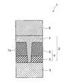
- FIG. 1is a schematic cross-sectional view for illustrating a nonvolatile memory device according to a first embodiment.
- FIG. 1the portion of a memory cell is mainly shown, and commonly known word lines, bit lines, protection films, interlayer insulating films, contacts, peripheral circuit units, etc. provided in a nonvolatile memory device 1 are omitted.
- the nonvolatile memory device 1includes a first electrode 3 , a memory cell 2 , and a second electrode 8 .
- the first electrode 3is formed of a conductive material.
- the conductive materialis not particularly limited; for example, tungsten (W), tungsten nitride (WN), tungsten carbide (WC), titanium (Ti), titanium nitride (TiN), copper (Cu), aluminum (Al), molybdenum (Mo), tantalum (Ta), silicide, silicon doped with a dopant element, and the like may be illustrated.
- the second electrode 8is provided on an ion supply unit 7 described later.
- the second electrode 8is formed of a conductive material.
- the material of the second electrode 8may be similar to the material of the first electrode 3 .
- the first electrode 3 and the second electrode 8are connected to a not-shown word line and a not-shown bit line.
- first electrode 3 and the second electrode 8are used as a word line and a bit line.
- a memory unit 4 and an ion supply unit 7are provided in the memory cell 2 provided between the first electrode 3 and the second electrode 8 .
- the memory unit 4includes a retention unit 5 and a resistance change unit 6 .
- the retention unit 5is provided on the first electrode 3 .
- the retention unit 5traps electrons moving from a conduction path 7 a described later toward the first electrode 3 side. Alternatively, the retention unit 5 traps electrons from the first electrode 3 side.
- the retention unit 5has electron traps that trap electrons.
- the retention unit 5may include a metal oxide having electron traps.
- the retention unit 5may be formed of a metal oxide or the like having a defect caused by oxygen deficiency or the like.
- the metal oxidemay be hafnium oxide (HfO x ), silicon oxynitride (SiO x N y ), aluminum oxide (Al x O y ), lanthanum oxide (La x O y ), tantalum oxide (Ta x O y ), strontium oxide (Sr x O y ), yttrium oxide (Y x O y ), barium oxide (Ba x O y ), zinc oxide (Zn x O y ), or the like.
- HfO xhafnium oxide
- SiO x N ysilicon oxynitride
- Al x O yaluminum oxide
- La x O ylanthanum oxide
- Ta x O ytantalum oxide
- strontium oxideSr x O y
- Y x O yyttrium oxide
- barium oxideBa x O y
- zinc oxideZn x O y
- the retention unit 5may be formed of one layer, or may have a configuration in which a plurality of layers is stacked.
- the retention unit 5may have a configuration in which a layer formed of silicon oxide (SiO x ) and a layer formed of any of the metal oxides described above are stacked.
- the retention unit 5may include a layer including silicon oxide (SiO x ) and a layer including at least one selected from the group consisting of hafnium oxide (HfO x ), silicon oxynitride (SiO x N y ), aluminum oxide (Al x O y ), lanthanum oxide (La x O y ), tantalum oxide (Ta x O y ), strontium oxide (Sr x O y ), yttrium oxide (Y x O y ), barium oxide (Ba x O y ), and zinc oxide (Zn x O y ).
- hafnium oxideHfO x
- silicon oxynitrideSiO x N y
- Al x O yaluminum oxide
- La x O ylanthanum oxide
- Ta x O ytantalum oxide
- strontium oxideSr x O y
- Y x O yyttrium oxide
- electronscan be trapped in electron traps in each layer and electrons can be trapped also in electron traps generated at the interface between layers.
- the electron trap density of the retention unit 5is preferably set to 1 ⁇ 10 11 /cm 3 or more.
- the electron trap density of the retention unit 5By setting the electron trap density of the retention unit 5 to 1 ⁇ 10 11 /cm 3 or more, ionization of the metal forming the conduction path 7 a described later can be sufficiently prevented.
- the electron trap density of the retention unit 5is preferably set to 1 ⁇ 10 13 /cm 3 or less.
- the dielectric constant of the retention unit 5is preferably set higher than the dielectric constant of the resistance change unit 6 . Thereby, a high voltage can be applied and therefore the formation of the conduction path 7 a described later becomes easy.
- the retention unit 5may include, for example, at least one selected from the group consisting of a metal oxide having a higher dielectric constant than silicon oxide, a metal nitride having a higher dielectric constant than silicon oxide, and a mixture of a metal oxide and a metal nitride having a higher dielectric constant than silicon oxide.
- the retention unit 5may have a configuration in which a plurality of layers made of these materials is stacked.
- the plurality of layersmay each include at least one of mutually different ones selected from the group consisting of a metal oxide having a higher dielectric constant than silicon oxide, a metal nitride having a higher dielectric constant than silicon oxide, and a mixture of a metal oxide and a metal nitride having a higher dielectric constant than silicon oxide.
- the resistance change unit 6is provided on the retention unit 5 .
- the resistance change unit 6is formed of a material having a high resistance and not interfering with the diffusion of ions from the ion supply unit 7 .
- the resistance change unit 6may be formed of amorphous silicon, silicon oxide, or the like.
- the ion supply unit 7is provided between the resistance change unit 6 and the second electrode 8 .
- the ion supply unit 7diffuses metal ions into the resistance change unit 6 , and precipitates a metal from the diffused metal ions to form a conduction path in the resistance change unit 6 .
- the ion supply unit 7may be formed of, for example, a metal such as silver (Ag), copper (Cu), cobalt (Co), nickel (Ni), aluminum (Al), or titanium (Ti), an alloy of them, or the like.
- a metalsuch as silver (Ag), copper (Cu), cobalt (Co), nickel (Ni), aluminum (Al), or titanium (Ti), an alloy of them, or the like.
- FIGS. 2A to 2Care schematic cross-sectional views for illustrating the operation of a nonvolatile memory device 101 according to a comparative example.
- FIGS. 2A to 2Cthe operation of a memory cell 102 is mainly illustrated.
- the nonvolatile memory device 101includes a first electrode 103 , a memory cell 102 , and a second electrode 108 .
- the memory cell 102includes a resistance change unit 106 and an ion supply unit 107 .
- first electrode 103the ion supply unit 107 , and the second electrode 108 may be similar to the first electrode 3 , the ion supply unit 7 , and the second electrode 8 described above, respectively.
- the resistance change unit 106which is a memory unit in the nonvolatile memory device 101 , may be similar to the resistance change unit 6 described above.
- the nonvolatile memory device 101 according to the comparative exampleis the case where the retention unit 5 is not provided.
- a voltageis applied such that the first electrode 103 becomes a negative pole and the second electrode 108 becomes a positive pole.
- the metal forming the ion supply unit 107changes to positive ions, the ions move toward the negative pole (the first electrode 103 ) side due to the electric field, and the ionized metal precipitates.
- a conduction path 107 ais formed in the resistance change unit 106 .
- a voltageis applied such that the first electrode 103 becomes a positive pole and the second electrode 108 becomes a negative pole.
- the metal forming the conduction path 107 ais ionized and the conduction path 107 a becomes short or disappears.
- At least two resistance statescan be created, and data can therefore be stored.
- the conduction path 107 amay become short even when no voltage is applied between the first electrode 103 and the second electrode 108 .
- electronsmay move from a portion where the conduction path 107 a and the first electrode 103 are in contact or from the conduction path 107 a near the portion toward the first electrode 103 side, and the metal forming the conduction path 107 a may be ionized.
- the metal forming the conduction path 107 ais silver (Ag)
- Agbecomes a Ag ion (Ag + )+an electron (e ⁇ ); the electron (e ⁇ ) moves toward the first electrode 103 side and the silver (Ag) changes to the Ag ion.
- the nonvolatile memory device 1includes the retention unit 5 , and can therefore retain a prescribed resistance state for a long time.
- FIG. 3is a schematic cross-sectional view for illustrating the operation of the nonvolatile memory device 1 .
- a voltageis applied such that the first electrode 3 becomes a negative pole and the second electrode 8 becomes a positive pole.
- the metal forming the ion supply unit 7e.g. silver (Ag)
- the metal forming the ion supply unit 7is ionized, and diffuses in the resistance change unit 6 toward the first electrode 3 side due to the electric field.
- the metal ions diffused in the resistance change unit 6receive electrons near the first electrode 3 , and precipitate as a metal again.
- a conduction path 7 ais formed in the resistance change unit 6 as shown in FIG. 3 .
- a voltageis applied such that the first electrode 3 becomes a positive pole and the second electrode 8 becomes a negative pole.
- the metal forming the conduction path 7 ais ionized and the conduction path 7 a becomes short or furthermore disappears.
- At least two resistance statescan be created, and data can therefore be stored.
- the metal forming the conduction path 7 ais ionized to separate the conduction path 7 a and the first electrode 3 . Consequently, a prescribed resistance state cannot be retained for a long time, and data retention properties may be degraded.
- the retention unit 5 having electron traps that trap electronsis provided on the first electrode 3 .
- FIGS. 4A to 4Eare schematic process cross-sectional views for illustrating a method for manufacturing the nonvolatile memory device 1 .
- FIGS. 4A to 4Eillustrate the case of manufacturing a cross-point nonvolatile memory device 1 .
- Arrows X, Y, and Z in FIGS. 4A to 4Eindicate three orthogonal directions; for example, X and Y indicate directions parallel to the major surface of a substrate and Z indicates the direction perpendicular to the major surface of the substrate.
- a stacked body 21 before processed into the configuration of the memory cell 2is formed.
- a film 23 that forms the first electrode 3is stacked in this order to form the stacked body 21 .
- Heat treatment etc.may be performed in the formation of the layers as necessary.
- the materials of the layersmay be similar to those described above.
- the formation of the film 23 that forms the first electrode 3 , the film 26 that forms the resistance change unit 6 , and the film 27 that forms the ion supply unit 7may be performed using, for example, a known film-formation method such as the sputtering method or the chemical vapor deposition (CVD) method.
- a known film-formation methodsuch as the sputtering method or the chemical vapor deposition (CVD) method.
- the retention unit 5is configured to have electron traps that trap electrons.
- the film 25 that forms the retention unit 5is formed of a material in which electron traps are formed.
- the material in which electron traps are formedmay be similar to those described above.
- hafnium oxideHfO x
- silicon oxynitrideSiO x N y
- aluminum oxideAl x O y
- lanthanum oxideLa x O y
- tantalum oxideTa x O y
- strontium oxideSr x O y
- Y x O yyttrium oxide
- barium oxideBa x O y
- zinc oxideZn x
- the formation of the film 25 that forms the retention unit 5may be performed using, for example, the sputtering method, the low pressure chemical vapor deposition (LPCVD) method, the atomic layer deposition (ALD) method, or the like.
- LPCVDlow pressure chemical vapor deposition
- ALDatomic layer deposition
- ion implantationmay be performed to make a defect caused by oxygen deficiency or the like to form electron traps.
- the density of electron traps included in the retention unit 5can be controlled.
- the density of electron trapscan be controlled to set the electron trap density of the retention unit 5 to 1 ⁇ 10 11 /cm 3 or more.
- the density of electron trapscan be controlled to set the electron trap density of the retention unit 5 to 1 ⁇ 10 13 /cm 3 or less.
- oxygen ionsmay be implanted.
- trenches 21 aare formed in the stacked body 21 .
- the formation of the trench 21 amay be performed using, for example, the PEP (photo-engraving process) and the RIE (reactive ion etching) method or the like.
- FIG. 4Billustrates a cross section of the stacked body 21 taken substantially perpendicular to the X direction.
- the stacked body 21is separated by the trench 21 a in the Y direction. Furthermore, the first electrode 3 in a stripe shape extending in the X direction is formed on the substrate 20 .
- the etching conditions in the etching processing of the layersare appropriately selected in accordance with the materials of the layers etc.
- the gas for etching, electric discharge conditions, etc.are appropriately altered in accordance with the materials of the layers etc.
- an insulatoris buried in the trench 21 a to form an element isolation unit 30 a.
- the formation of the element isolation unit 30 amay be performed using an application method such as the spin coating method.
- a perhydropolysilazane (PHPS) solutionwhich is a polysilazane-based material, may be applied using the spin coating method to form an element isolation unit 30 a including silicon oxide (SiO 2 ) as a main component in the trench 21 a.
- PHPSperhydropolysilazane
- the physical vapor deposition (PVD) methodfor the formation of the element isolation unit 30 a , also the physical vapor deposition (PVD) method, the chemical vapor deposition method, or the like may be used.
- PVDphysical vapor deposition
- CVDchemical vapor deposition
- the CMP (chemical mechanical polishing) method or the likeis used to planarize the surface of the stacked body 21 in which the element isolation unit 30 a is formed.
- trenches 21 bare formed in the stacked body 21 .
- FIG. 4Dillustrates a cross section of the stacked body 21 taken substantially perpendicular to the Y direction.
- the stacked body 21is separated by the trench 21 a described above in the Y direction and is separated by the trench 21 b in the X direction.
- an insulatoris buried in the trench 21 b to form an element isolation unit 30 b.
- the formation of the element isolation unit 30 bmay be similar to the formation of the element isolation unit 30 a described above.
- the CMP method or the likeis used to planarize the surface of the stacked body 21 in which the element isolation unit 30 b is formed.
- a film that forms the second electrode 8is formed on the stacked body 21 , and the second electrode 8 in a stripe shape extending in the Y direction is formed on the stacked body 21 using the PEP and the RIE (reactive ion etching) method or the like.
- the memory cell 2can be formed at the intersection of the first electrode 3 in a stripe shape extending in the X direction and the second electrode 8 in a stripe shape extending in the Y direction.
- one of the first electrode 3 in a stripe shape and the second electrode 8 in a stripe shapemay be used as a word line, and the other may be used as a bit line.
- a cross-point nonvolatile memory device 1can be manufactured.
- an insulating layermay be provided between vertically adjacent memory cells 2 .
- the first electrode 3 or the second electrode 8may be shared between vertically adjacent memory cells 2 .
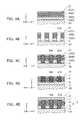
- FIG. 5is a schematic cross-sectional view for illustrating an example of memory cells 2 stacked.
- the second electrode 8when the second electrode 8 is shared between vertically adjacent memory cells 2 , the downsizing of the nonvolatile memory device, the simplification of manufacturing processes, etc. can be achieved.
- first electrode 3it is also possible for the first electrode 3 to be shared between vertically adjacent memory cells 2 .
- the embodiments illustrated abovecan provide a nonvolatile memory device than can improve data retention properties and a method for manufacturing the same.
Landscapes
- Engineering & Computer Science (AREA)
- Manufacturing & Machinery (AREA)
- Semiconductor Memories (AREA)
Abstract
Description
- This application is based upon and claims the benefit of priority from the prior Japanese Patent Application No. 2011-278990, filed on Dec. 20, 2011; the entire contents of which are incorporated herein by reference.
- Embodiments described herein relate generally to a nonvolatile memory device and a method for manufacturing the same.
- There is a nonvolatile memory device in which a resistance change unit and an ion supply unit are provided between two electrodes.
- In such a nonvolatile memory device, when a voltage is applied using the electrode on the ion supply unit side as a positive pole and the electrode on the resistance change unit side as a negative pole, a metal included in the ion supply unit is ionized to diffuse into the resistance change unit and receives electrons from the electrode on the negative pole side. Thereby, a conduction path (filament) of a metal is formed between the two electrodes. This leads to a situation where the resistance between the electrode on the ion supply unit side and the electrode on the resistance change unit side is low.
- On the other hand, when a voltage of the opposite polarity is applied, the metal forming the conduction path is ionized, and thereby the conduction path becomes short and furthermore disappears. This leads to a situation where the resistance between the electrode on the ion supply unit side and the electrode on the resistance change unit side is high.
- Thus, at least two resistance states can be created, and data can therefore be stored.
- However, in such a nonvolatile memory device, for example, there is a problem that the formed conduction path becomes short or something to change the resistance state even in a state where no voltage is applied.
- Hence, it is desired to develop a nonvolatile memory device in which the properties that resistance states can be retained for a long time (data retention properties) are high.
FIG. 1 is a schematic cross-sectional view for illustrating a nonvolatile memory device according to a first embodiment;FIGS. 2A to 2C are schematic cross-sectional views for illustrating the operation of anonvolatile memory device 101 according to a comparative example;FIG. 3 is a schematic cross-sectional view for illustrating the operation of thenonvolatile memory device 1;FIGS. 4A to 4E are schematic process cross-sectional views for illustrating a method for manufacturing thenonvolatile memory device 1; andFIG. 5 is a schematic cross-sectional view for illustrating an example ofmemory cells 2 stacked.- In general, according to one embodiment, a nonvolatile memory device includes a first electrode, a second electrode, and a memory cell provided between the first electrode and the second electrode. The memory cell includes a retention unit, a resistance change unit, and an ion supply unit. The retention unit is provided on the first electrode and has an electron trap. The resistance change unit is provided on the retention unit. The ion supply unit is provided between the resistance change unit and the second electrode and includes a metal element.
- Various embodiments will be illustrated hereinafter with reference to the accompanying drawings.
- In the drawings, similar components are marked with the same reference numerals, and a detailed description is omitted as appropriate.
FIG. 1 is a schematic cross-sectional view for illustrating a nonvolatile memory device according to a first embodiment.- In
FIG. 1 , the portion of a memory cell is mainly shown, and commonly known word lines, bit lines, protection films, interlayer insulating films, contacts, peripheral circuit units, etc. provided in anonvolatile memory device 1 are omitted. - As shown in
FIG. 1 , thenonvolatile memory device 1 includes afirst electrode 3, amemory cell 2, and asecond electrode 8. - The
first electrode 3 is formed of a conductive material. - The conductive material is not particularly limited; for example, tungsten (W), tungsten nitride (WN), tungsten carbide (WC), titanium (Ti), titanium nitride (TiN), copper (Cu), aluminum (Al), molybdenum (Mo), tantalum (Ta), silicide, silicon doped with a dopant element, and the like may be illustrated.
- The
second electrode 8 is provided on anion supply unit 7 described later. - The
second electrode 8 is formed of a conductive material. The material of thesecond electrode 8 may be similar to the material of thefirst electrode 3. - The
first electrode 3 and thesecond electrode 8 are connected to a not-shown word line and a not-shown bit line. - It is also possible to use the
first electrode 3 and thesecond electrode 8 as a word line and a bit line. - In the
memory cell 2 provided between thefirst electrode 3 and thesecond electrode 8, amemory unit 4 and anion supply unit 7 are provided. - The
memory unit 4 includes aretention unit 5 and aresistance change unit 6. - The
retention unit 5 is provided on thefirst electrode 3. - The
retention unit 5 traps electrons moving from aconduction path 7adescribed later toward thefirst electrode 3 side. Alternatively, theretention unit 5 traps electrons from thefirst electrode 3 side. - Thus, the
retention unit 5 has electron traps that trap electrons. - For example, the
retention unit 5 may include a metal oxide having electron traps. - For example, the
retention unit 5 may be formed of a metal oxide or the like having a defect caused by oxygen deficiency or the like. - In this case, the metal oxide may be hafnium oxide (HfOx), silicon oxynitride (SiOxNy), aluminum oxide (AlxOy), lanthanum oxide (LaxOy), tantalum oxide (TaxOy), strontium oxide (SrxOy), yttrium oxide (YxOy), barium oxide (BaxOy), zinc oxide (ZnxOy), or the like.
- The
retention unit 5 may be formed of one layer, or may have a configuration in which a plurality of layers is stacked. - For example, the
retention unit 5 may have a configuration in which a layer formed of silicon oxide (SiOx) and a layer formed of any of the metal oxides described above are stacked. - In this case, the
retention unit 5 may include a layer including silicon oxide (SiOx) and a layer including at least one selected from the group consisting of hafnium oxide (HfOx), silicon oxynitride (SiOxNy), aluminum oxide (AlxOy), lanthanum oxide (LaxOy), tantalum oxide (TaxOy), strontium oxide (SrxOy), yttrium oxide (YxOy), barium oxide (BaxOy), and zinc oxide (ZnxOy). - By using the
retention unit 5 in which a plurality of layers are stacked, electrons can be trapped in electron traps in each layer and electrons can be trapped also in electron traps generated at the interface between layers. - According to the findings obtained by the inventors, the electron trap density of the
retention unit 5 is preferably set to 1×10¹¹/cm3or more. - By setting the electron trap density of the
retention unit 5 to 1×10¹¹/cm3or more, ionization of the metal forming theconduction path 7adescribed later can be sufficiently prevented. - Consequently, since a prescribed resistance state can be retained for a long time, data retention properties can be improved.
- The electron trap density of the
retention unit 5 is preferably set to 1×10¹³/cm3or less. - If the electron trap density of the
retention unit 5 exceeds 1×10¹³/cm3, a leak current may be likely to occur. - The dielectric constant of the
retention unit 5 is preferably set higher than the dielectric constant of theresistance change unit 6. Thereby, a high voltage can be applied and therefore the formation of theconduction path 7adescribed later becomes easy. - The
retention unit 5 may include, for example, at least one selected from the group consisting of a metal oxide having a higher dielectric constant than silicon oxide, a metal nitride having a higher dielectric constant than silicon oxide, and a mixture of a metal oxide and a metal nitride having a higher dielectric constant than silicon oxide. Alternatively, theretention unit 5 may have a configuration in which a plurality of layers made of these materials is stacked. - In the case where a plurality of layers are stacked, the plurality of layers may each include at least one of mutually different ones selected from the group consisting of a metal oxide having a higher dielectric constant than silicon oxide, a metal nitride having a higher dielectric constant than silicon oxide, and a mixture of a metal oxide and a metal nitride having a higher dielectric constant than silicon oxide.
- Details of the operation and effect of the
retention unit 5 are described later. - The
resistance change unit 6 is provided on theretention unit 5. - The
resistance change unit 6 is formed of a material having a high resistance and not interfering with the diffusion of ions from theion supply unit 7. - For example, the
resistance change unit 6 may be formed of amorphous silicon, silicon oxide, or the like. - The
ion supply unit 7 is provided between theresistance change unit 6 and thesecond electrode 8. - The
ion supply unit 7 diffuses metal ions into theresistance change unit 6, and precipitates a metal from the diffused metal ions to form a conduction path in theresistance change unit 6. - The
ion supply unit 7 may be formed of, for example, a metal such as silver (Ag), copper (Cu), cobalt (Co), nickel (Ni), aluminum (Al), or titanium (Ti), an alloy of them, or the like. - Next, the operation of the
nonvolatile memory device 1 and the operation and effect of theretention unit 5 are illustrated. FIGS. 2A to 2C are schematic cross-sectional views for illustrating the operation of anonvolatile memory device 101 according to a comparative example.- In
FIGS. 2A to 2C , the operation of amemory cell 102 is mainly illustrated. - As shown in
FIG. 2A , thenonvolatile memory device 101 according to the comparative example includes afirst electrode 103, amemory cell 102, and asecond electrode 108. - The
memory cell 102 includes aresistance change unit 106 and anion supply unit 107. - Here, the
first electrode 103, theion supply unit 107, and thesecond electrode 108 may be similar to thefirst electrode 3, theion supply unit 7, and thesecond electrode 8 described above, respectively. - Furthermore, the
resistance change unit 106, which is a memory unit in thenonvolatile memory device 101, may be similar to theresistance change unit 6 described above. - That is, the
nonvolatile memory device 101 according to the comparative example is the case where theretention unit 5 is not provided. - In the
nonvolatile memory device 101 thus configured, a voltage is applied such that thefirst electrode 103 becomes a negative pole and thesecond electrode 108 becomes a positive pole. - Thereby, as shown in
FIG. 2B , the metal forming the ion supply unit107 (e.g. silver (Ag)) changes to positive ions, the ions move toward the negative pole (the first electrode103) side due to the electric field, and the ionized metal precipitates. Thus, aconduction path 107ais formed in theresistance change unit 106. - When the
conduction path 107ais formed, a situation is created where the resistance between thefirst electrode 103 and thesecond electrode 108 is low. - Further, in the state where the
conduction path 107ais formed, a voltage is applied such that thefirst electrode 103 becomes a positive pole and thesecond electrode 108 becomes a negative pole. - Thereby, the metal forming the
conduction path 107ais ionized and theconduction path 107abecomes short or disappears. - When the
conduction path 107abecomes short or disappears, the situation becomes one where the resistance between thefirst electrode 103 and thesecond electrode 108 is high. - Thus, at least two resistance states can be created, and data can therefore be stored.
- Here, in the state where the
conduction path 107ais formed, theconduction path 107amay become short even when no voltage is applied between thefirst electrode 103 and thesecond electrode 108. - For example, electrons may move from a portion where the
conduction path 107aand thefirst electrode 103 are in contact or from theconduction path 107anear the portion toward thefirst electrode 103 side, and the metal forming theconduction path 107amay be ionized. - For example, in the case where the metal forming the
conduction path 107ais silver (Ag), Ag becomes a Ag ion (Ag+)+an electron (e−); the electron (e−) moves toward thefirst electrode 103 side and the silver (Ag) changes to the Ag ion. - When such a reaction occurs continuously, as shown in
FIG. 2C , theconduction path 107aand thefirst electrode 103 are separated, and a low resistance state cannot be retained. - That is, a prescribed resistance state cannot be retained for a long time, and data retention properties may be degraded.
- In contrast, the
nonvolatile memory device 1 according to the embodiment includes theretention unit 5, and can therefore retain a prescribed resistance state for a long time. - Next, the operation of the
nonvolatile memory device 1 according to the embodiment and the operation and effect of theretention unit 5 are illustrated. FIG. 3 is a schematic cross-sectional view for illustrating the operation of thenonvolatile memory device 1.- In the
nonvolatile memory device 1, a voltage is applied such that thefirst electrode 3 becomes a negative pole and thesecond electrode 8 becomes a positive pole. - Thereby, the metal forming the ion supply unit7 (e.g. silver (Ag)) is ionized, and diffuses in the
resistance change unit 6 toward thefirst electrode 3 side due to the electric field. The metal ions diffused in theresistance change unit 6 receive electrons near thefirst electrode 3, and precipitate as a metal again. - By the ionization, diffusion, and precipitation of the metal forming the
ion supply unit 7 being repeated, aconduction path 7ais formed in theresistance change unit 6 as shown inFIG. 3 . - When the
conduction path 7ais formed, a situation is created where the resistance between thefirst electrode 3 and thesecond electrode 8 is low. - Further, in the state where the
conduction path 7ais formed, a voltage is applied such that thefirst electrode 3 becomes a positive pole and thesecond electrode 8 becomes a negative pole. - Thereby, the metal forming the
conduction path 7ais ionized and theconduction path 7abecomes short or furthermore disappears. - When the
conduction path 7abecomes short or disappears, the situation becomes one where the resistance between thefirst electrode 3 and thesecond electrode 8 is high. - Thus, at least two resistance states can be created, and data can therefore be stored.
- Here, when electrons move from a portion where the
conduction path 7aand thefirst electrode 3 are in contact or from theconduction path 7anear the portion toward thefirst electrode 3 side, the metal forming theconduction path 7ais ionized to separate theconduction path 7aand thefirst electrode 3. Consequently, a prescribed resistance state cannot be retained for a long time, and data retention properties may be degraded. - In view of this, in the
nonvolatile memory device 1 according to the embodiment, theretention unit 5 having electron traps that trap electrons is provided on thefirst electrode 3. - When electrons that have moved from the
conduction path 7aare trapped in electron traps included in theretention unit 5, an equilibrium state is formed between the electrons trapped in the electron traps and the electrons moving from theconduction path 7a. - In the case of the
retention unit 5 in which a plurality of layers are stacked, electrons are trapped in electron traps in each layer and electrons are trapped also at the interface between layers. - Therefore, the movement of electrons from the
conduction path 7atoward thefirst electrode 3 side is suppressed, and the metal forming theconduction path 7acan thus be prevented from being ionized. - Consequently, since a prescribed resistance state can be retained for a long time, data retention properties can be improved.
- Next, a method for manufacturing the
nonvolatile memory device 1 is illustrated. FIGS. 4A to 4E are schematic process cross-sectional views for illustrating a method for manufacturing thenonvolatile memory device 1.FIGS. 4A to 4E illustrate the case of manufacturing a cross-pointnonvolatile memory device 1.- Since known art can be applied to the formation of peripheral circuit units etc. provided in the
nonvolatile memory device 1, the illustration of them is omitted and herein the formation of thememory cell 2 is mainly illustrated. - Arrows X, Y, and Z in
FIGS. 4A to 4E indicate three orthogonal directions; for example, X and Y indicate directions parallel to the major surface of a substrate and Z indicates the direction perpendicular to the major surface of the substrate. - First, as shown in
FIG. 4A , astacked body 21 before processed into the configuration of thememory cell 2 is formed. - That is, on the major surface of a
substrate 20 such as a wafer, afilm 23 that forms thefirst electrode 3, afilm 25 that forms theretention unit 5, afilm 26 that forms theresistance change unit 6, and afilm 27 that forms theion supply unit 7 are stacked in this order to form the stackedbody 21. Heat treatment etc. may be performed in the formation of the layers as necessary. - The materials of the layers may be similar to those described above.
- The formation of the
film 23 that forms thefirst electrode 3, thefilm 26 that forms theresistance change unit 6, and thefilm 27 that forms theion supply unit 7 may be performed using, for example, a known film-formation method such as the sputtering method or the chemical vapor deposition (CVD) method. - As described above, the
retention unit 5 is configured to have electron traps that trap electrons. - Hence, the
film 25 that forms theretention unit 5 is formed of a material in which electron traps are formed. - The material in which electron traps are formed may be similar to those described above.
- For example, in the process of forming the
film 25 that forms theretention unit 5, afilm 25 including at least one selected from the group consisting of hafnium oxide (HfOx), silicon oxynitride (SiOxNy), aluminum oxide (AlxOy), lanthanum oxide (LaxOy), tantalum oxide (TaxOy), strontium oxide (SrxOy), yttrium oxide (YxOy), barium oxide (BaxOy), and zinc oxide (ZnxOy) may be formed. - The formation of the
film 25 that forms theretention unit 5 may be performed using, for example, the sputtering method, the low pressure chemical vapor deposition (LPCVD) method, the atomic layer deposition (ALD) method, or the like. - After the film-formation of the
film 25 that forms theretention unit 5, for example, ion implantation may be performed to make a defect caused by oxygen deficiency or the like to form electron traps. - In the case where ion implantation is performed after the film-formation of the
film 25 that forms theretention unit 5, the density of electron traps included in theretention unit 5 can be controlled. - When ion implantation is performed, for example, the density of electron traps can be controlled to set the electron trap density of the
retention unit 5 to 1×10¹¹/cm3or more. - Furthermore, when ion implantation is performed, for example, the density of electron traps can be controlled to set the electron trap density of the
retention unit 5 to 1×10¹³/cm3or less. - In the ion implantation, for example, oxygen ions may be implanted.
- Next, as shown in
FIG. 4B ,trenches 21aare formed in the stackedbody 21. - The formation of the
trench 21amay be performed using, for example, the PEP (photo-engraving process) and the RIE (reactive ion etching) method or the like. FIG. 4B illustrates a cross section of the stackedbody 21 taken substantially perpendicular to the X direction.- Thereby, the
stacked body 21 is separated by thetrench 21ain the Y direction. Furthermore, thefirst electrode 3 in a stripe shape extending in the X direction is formed on thesubstrate 20. - The etching conditions in the etching processing of the layers are appropriately selected in accordance with the materials of the layers etc.
- For example, the gas for etching, electric discharge conditions, etc. are appropriately altered in accordance with the materials of the layers etc.
- Next, as shown in
FIG. 4C , an insulator is buried in thetrench 21ato form anelement isolation unit 30a. - The formation of the
element isolation unit 30amay be performed using an application method such as the spin coating method. For example, a perhydropolysilazane (PHPS) solution, which is a polysilazane-based material, may be applied using the spin coating method to form anelement isolation unit 30aincluding silicon oxide (SiO2) as a main component in thetrench 21a. - For the formation of the
element isolation unit 30a, also the physical vapor deposition (PVD) method, the chemical vapor deposition method, or the like may be used. - After that, the CMP (chemical mechanical polishing) method or the like is used to planarize the surface of the stacked
body 21 in which theelement isolation unit 30ais formed. - Next, as shown in
FIG. 4D ,trenches 21bare formed in the stackedbody 21. - The formation of the
trench 21bmay be similar to the formation of thetrench 21adescribed above.FIG. 4D illustrates a cross section of the stackedbody 21 taken substantially perpendicular to the Y direction. - The
stacked body 21 is separated by thetrench 21adescribed above in the Y direction and is separated by thetrench 21bin the X direction. - After that, an insulator is buried in the
trench 21bto form anelement isolation unit 30b. - The formation of the
element isolation unit 30bmay be similar to the formation of theelement isolation unit 30adescribed above. - The CMP method or the like is used to planarize the surface of the stacked
body 21 in which theelement isolation unit 30bis formed. - Next, as shown in
FIG. 4E , a film that forms thesecond electrode 8 is formed on thestacked body 21, and thesecond electrode 8 in a stripe shape extending in the Y direction is formed on thestacked body 21 using the PEP and the RIE (reactive ion etching) method or the like. - In this way, the
memory cell 2 can be formed at the intersection of thefirst electrode 3 in a stripe shape extending in the X direction and thesecond electrode 8 in a stripe shape extending in the Y direction. - In this case, one of the
first electrode 3 in a stripe shape and thesecond electrode 8 in a stripe shape may be used as a word line, and the other may be used as a bit line. - Thus, a cross-point
nonvolatile memory device 1 can be manufactured. - What are illustrated in the first embodiment and the second embodiment are cases where one layer of
memory cells 2 is provided, but a plurality ofmemory cells 2 may be provided to be stacked. - In the case where
memory cells 2 are stacked, an insulating layer may be provided between verticallyadjacent memory cells 2. - The
first electrode 3 or thesecond electrode 8 may be shared between verticallyadjacent memory cells 2. FIG. 5 is a schematic cross-sectional view for illustrating an example ofmemory cells 2 stacked.- As shown in
FIG. 5 , when thesecond electrode 8 is shared between verticallyadjacent memory cells 2, the downsizing of the nonvolatile memory device, the simplification of manufacturing processes, etc. can be achieved. - It is also possible for the
first electrode 3 to be shared between verticallyadjacent memory cells 2. - The embodiments illustrated above can provide a nonvolatile memory device than can improve data retention properties and a method for manufacturing the same.
- While certain embodiments have been described, these embodiments have been presented by way of example only, and are not intended to limit the scope of the inventions. Indeed, the novel embodiments described herein may be embodied in a variety of other forms; furthermore, various omissions, substitutions and changes in the form of the embodiments described herein may be made without departing from the spirit of the inventions. The accompanying claims and their equivalents are intended to cover such forms or modifications as would fall within the scope and spirit of the inventions. Moreover, above-mentioned embodiments can be combined mutually and can be carried out.
Claims (20)
Applications Claiming Priority (2)
| Application Number | Priority Date | Filing Date | Title |
|---|---|---|---|
| JP2011-278990 | 2011-12-20 | ||
| JP2011278990AJP5480233B2 (en) | 2011-12-20 | 2011-12-20 | Nonvolatile memory device and manufacturing method thereof |
Publications (2)
| Publication Number | Publication Date |
|---|---|
| US20130153850A1true US20130153850A1 (en) | 2013-06-20 |
| US9142774B2 US9142774B2 (en) | 2015-09-22 |
Family
ID=48609197
Family Applications (1)
| Application Number | Title | Priority Date | Filing Date |
|---|---|---|---|
| US13/715,180ActiveUS9142774B2 (en) | 2011-12-20 | 2012-12-14 | Nonvolatile memory device and method for manufacturing the same |
Country Status (3)
| Country | Link |
|---|---|
| US (1) | US9142774B2 (en) |
| JP (1) | JP5480233B2 (en) |
| CN (1) | CN103178067B (en) |
Cited By (3)
| Publication number | Priority date | Publication date | Assignee | Title |
|---|---|---|---|---|
| US9634245B2 (en) | 2015-01-09 | 2017-04-25 | Micron Technology, Inc. | Structures incorporating and methods of forming metal lines including carbon |
| US9647207B2 (en) | 2015-01-26 | 2017-05-09 | Taiwan Semiconductor Manufacturing Co., Ltd. | Resistive random access memory (RRAM) structure |
| US10832911B2 (en)* | 2018-09-22 | 2020-11-10 | Toyoda Gosei Co., Ltd. | Semiconductor device |
Families Citing this family (7)
| Publication number | Priority date | Publication date | Assignee | Title |
|---|---|---|---|---|
| JP6430306B2 (en)* | 2015-03-19 | 2018-11-28 | 東芝メモリ株式会社 | Nonvolatile memory device |
| CN106410024A (en)* | 2015-08-03 | 2017-02-15 | 华邦电子股份有限公司 | Resistive random access memory |
| CN105390611B (en)* | 2015-10-16 | 2019-01-18 | 福州大学 | A kind of low-power consumption resistance-variable storing device and preparation method thereof based on double storage medium layers |
| CN108400237B (en)* | 2017-02-07 | 2022-01-14 | 华邦电子股份有限公司 | Conductive bridging random access memory and manufacturing method thereof |
| CN109273597B (en)* | 2018-08-29 | 2021-02-02 | 西北工业大学 | A kind of SrO-based resistive memory and preparation method thereof |
| JP2020047681A (en) | 2018-09-15 | 2020-03-26 | キオクシア株式会社 | Semiconductor storage device |
| CN112216791B (en)* | 2019-07-10 | 2022-11-22 | 中国科学院化学研究所 | A silicon oxide-based memristor based on a solution method and its preparation method and application |
Citations (41)
| Publication number | Priority date | Publication date | Assignee | Title |
|---|---|---|---|---|
| US20060054950A1 (en)* | 2004-09-10 | 2006-03-16 | In-Gyu Baek | Non-volatile memory cells employing a transition metal oxide layer as a data storage material layer and methods of manufacturing the same |
| JP2007165474A (en)* | 2005-12-12 | 2007-06-28 | Sony Corp | Storage element and storage device |
| US20070252193A1 (en)* | 2006-04-28 | 2007-11-01 | Samsung Electronics Co., Ltd. | Non-volatile memory devices including variable resistance material |
| US20080007988A1 (en)* | 2006-07-10 | 2008-01-10 | Samsung Electronics Co., Ltd. | Non-volatile memory device including variable resistance material and method of fabricating the same |
| US20080280415A1 (en)* | 2007-05-09 | 2008-11-13 | Elpida Memory, Inc. | Method of manufacturing semiconductor memory device |
| US20090014770A1 (en)* | 2007-07-12 | 2009-01-15 | Hitachi, Ltd. | Semiconductor device |
| US20090026434A1 (en)* | 2007-07-25 | 2009-01-29 | Malhotra Sandra G | Nonvolatile memory elements |
| US20090272961A1 (en)* | 2008-05-01 | 2009-11-05 | Michael Miller | Surface treatment to improve resistive-switching characteristics |
| US20090272962A1 (en)* | 2008-05-01 | 2009-11-05 | Pragati Kumar | Reduction of forming voltage in semiconductor devices |
| US20100006813A1 (en)* | 2008-07-10 | 2010-01-14 | Seagate Technology Llc | Programmable metallization memory cells via selective channel forming |
| US20100187595A1 (en)* | 2009-01-28 | 2010-07-29 | Samsung Electronics Co., Ltd. | Nonvolatile memory devices and methods of manufacturing the same |
| US20100230655A1 (en)* | 2007-12-06 | 2010-09-16 | Fujitsu Limited | Variable resistance device, method for manufacturing variable resistance device, and semiconductor storage device using variable resistance device |
| US20100240207A1 (en)* | 2009-03-19 | 2010-09-23 | Samsung Electronics Co., Ltd. | Methods of manufacturing charge trap type memory devices |
| US20100243983A1 (en)* | 2009-03-31 | 2010-09-30 | Tony Chiang | Controlled localized defect paths for resistive memories |
| US20100265750A1 (en)* | 2009-04-20 | 2010-10-21 | Tianhong Yan | Memory system with data line switching scheme |
| US20100288995A1 (en)* | 2009-05-14 | 2010-11-18 | Yoshio Ozawa | Semiconductor memory device and method of manufacturing the same |
| US20100327253A1 (en)* | 2009-06-30 | 2010-12-30 | Kabushiki Kaisha Toshiba | Nonvolatile semiconductor memory device |
| US20110095259A1 (en)* | 2009-10-23 | 2011-04-28 | Lee Yu-Jin | Resistance changing device and method for fabricating the same |
| US20110108829A1 (en)* | 2007-12-19 | 2011-05-12 | Naoki Banno | Switching device and method of manufacturing the same |
| US20110147825A1 (en)* | 2008-11-18 | 2011-06-23 | Samsung Electronics Co., Ltd. | Nonvolatile memory devices including deep and high density trapping layers |
| US20110194329A1 (en)* | 2010-02-09 | 2011-08-11 | Sony Corporation | Memory component, memory device, and method of operating memory device |
| US20110235419A1 (en)* | 2010-03-29 | 2011-09-29 | Renesas Electronics Corporation | Non-volatile semiconductor storage device |
| US20120015512A1 (en)* | 2008-01-02 | 2012-01-19 | Samsung Electronics Co., Ltd. | Method of manufacturing non-volatile memory device |
| US20120068144A1 (en)* | 2010-09-22 | 2012-03-22 | Kabushiki Kaisha Toshiba | Resistance random access memory |
| US20120068146A1 (en)* | 2010-09-16 | 2012-03-22 | Sony Corporation | Memory element and memory device |
| US20120243293A1 (en)* | 2011-03-22 | 2012-09-27 | Akira Takashima | Nonvolatile semiconductor memory device |
| US20120294063A1 (en)* | 2011-03-04 | 2012-11-22 | Sony Corporation | Memory element and memory device |
| US20120314479A1 (en)* | 2011-06-10 | 2012-12-13 | Sony Corporation | Memory element and memory device |
| US20130001503A1 (en)* | 2011-05-05 | 2013-01-03 | Gallo Antonio R | Conductive filament based memory elements and methods with improved data retention and/or endurance |
| US20130051116A1 (en)* | 2011-08-24 | 2013-02-28 | Advanced Micro Devices, Inc. | Integrated circuit with face-to-face bonded passive variable resistance memory and method for making the same |
| US20130051117A1 (en)* | 2011-08-24 | 2013-02-28 | Advanced Micro Devices, Inc. | Integrated circuit with vertically integrated passive variable resistance memory and method for making the same |
| US20130065377A1 (en)* | 2011-09-09 | 2013-03-14 | Intermolecular, Inc. | Interface layer improvements for nonvolatile memory applications |
| US20130070515A1 (en)* | 2011-09-16 | 2013-03-21 | Advanced Micro Devices, Inc. | Method and apparatus for controlling state information retention in an apparatus |
| US20130083048A1 (en)* | 2011-09-29 | 2013-04-04 | Advanced Micro Devices, Inc. | Integrated circuit with active memory and passive variable resistive memory with shared memory control logic and method of making same |
| US20130153845A1 (en)* | 2011-12-16 | 2013-06-20 | Intermolecular, Inc. | Nonvolatile resistive memory element with a metal nitride containing switching layer |
| US20130228735A1 (en)* | 2012-03-01 | 2013-09-05 | Intermolecular, Inc. | Interfacial oxide used as switching layer in a nonvolatile resistive memory element |
| US20130328009A1 (en)* | 2011-02-18 | 2013-12-12 | Kabushiki Kaisha Toshiba | Nonvolatile variable resistance element |
| US20140063901A1 (en)* | 2012-08-30 | 2014-03-06 | Adesto Technologies Corporation | Memory devices, circuits and, methods that apply different electrical conditions in access operations |
| US20140070160A1 (en)* | 2012-09-07 | 2014-03-13 | Takayuki Ishikawa | Nonvolatile memory device |
| US8829482B1 (en)* | 2010-09-23 | 2014-09-09 | Adesto Technologies Corporation | Variable impedance memory device structure and method of manufacture including programmable impedance memory cells and methods of forming the same |
| US8854873B1 (en)* | 2011-05-05 | 2014-10-07 | Adesto Technologies Corporation | Memory devices, architectures and methods for memory elements having dynamic change in property |
Family Cites Families (2)
| Publication number | Priority date | Publication date | Assignee | Title |
|---|---|---|---|---|
| KR101248941B1 (en) | 2006-03-11 | 2013-03-29 | 삼성전자주식회사 | Method of program and erasing of memory device |
| JP4816314B2 (en) | 2006-08-08 | 2011-11-16 | ソニー株式会社 | Storage element and storage device |
- 2011
- 2011-12-20JPJP2011278990Apatent/JP5480233B2/enactiveActive
- 2012
- 2012-12-14USUS13/715,180patent/US9142774B2/enactiveActive
- 2012-12-20CNCN201210557218.8Apatent/CN103178067B/enactiveActive
Patent Citations (41)
| Publication number | Priority date | Publication date | Assignee | Title |
|---|---|---|---|---|
| US20060054950A1 (en)* | 2004-09-10 | 2006-03-16 | In-Gyu Baek | Non-volatile memory cells employing a transition metal oxide layer as a data storage material layer and methods of manufacturing the same |
| JP2007165474A (en)* | 2005-12-12 | 2007-06-28 | Sony Corp | Storage element and storage device |
| US20070252193A1 (en)* | 2006-04-28 | 2007-11-01 | Samsung Electronics Co., Ltd. | Non-volatile memory devices including variable resistance material |
| US20080007988A1 (en)* | 2006-07-10 | 2008-01-10 | Samsung Electronics Co., Ltd. | Non-volatile memory device including variable resistance material and method of fabricating the same |
| US20080280415A1 (en)* | 2007-05-09 | 2008-11-13 | Elpida Memory, Inc. | Method of manufacturing semiconductor memory device |
| US20090014770A1 (en)* | 2007-07-12 | 2009-01-15 | Hitachi, Ltd. | Semiconductor device |
| US20090026434A1 (en)* | 2007-07-25 | 2009-01-29 | Malhotra Sandra G | Nonvolatile memory elements |
| US20100230655A1 (en)* | 2007-12-06 | 2010-09-16 | Fujitsu Limited | Variable resistance device, method for manufacturing variable resistance device, and semiconductor storage device using variable resistance device |
| US20110108829A1 (en)* | 2007-12-19 | 2011-05-12 | Naoki Banno | Switching device and method of manufacturing the same |
| US20120015512A1 (en)* | 2008-01-02 | 2012-01-19 | Samsung Electronics Co., Ltd. | Method of manufacturing non-volatile memory device |
| US20090272961A1 (en)* | 2008-05-01 | 2009-11-05 | Michael Miller | Surface treatment to improve resistive-switching characteristics |
| US20090272962A1 (en)* | 2008-05-01 | 2009-11-05 | Pragati Kumar | Reduction of forming voltage in semiconductor devices |
| US20100006813A1 (en)* | 2008-07-10 | 2010-01-14 | Seagate Technology Llc | Programmable metallization memory cells via selective channel forming |
| US20110147825A1 (en)* | 2008-11-18 | 2011-06-23 | Samsung Electronics Co., Ltd. | Nonvolatile memory devices including deep and high density trapping layers |
| US20100187595A1 (en)* | 2009-01-28 | 2010-07-29 | Samsung Electronics Co., Ltd. | Nonvolatile memory devices and methods of manufacturing the same |
| US20100240207A1 (en)* | 2009-03-19 | 2010-09-23 | Samsung Electronics Co., Ltd. | Methods of manufacturing charge trap type memory devices |
| US20100243983A1 (en)* | 2009-03-31 | 2010-09-30 | Tony Chiang | Controlled localized defect paths for resistive memories |
| US20100265750A1 (en)* | 2009-04-20 | 2010-10-21 | Tianhong Yan | Memory system with data line switching scheme |
| US20100288995A1 (en)* | 2009-05-14 | 2010-11-18 | Yoshio Ozawa | Semiconductor memory device and method of manufacturing the same |
| US20100327253A1 (en)* | 2009-06-30 | 2010-12-30 | Kabushiki Kaisha Toshiba | Nonvolatile semiconductor memory device |
| US20110095259A1 (en)* | 2009-10-23 | 2011-04-28 | Lee Yu-Jin | Resistance changing device and method for fabricating the same |
| US20110194329A1 (en)* | 2010-02-09 | 2011-08-11 | Sony Corporation | Memory component, memory device, and method of operating memory device |
| US20110235419A1 (en)* | 2010-03-29 | 2011-09-29 | Renesas Electronics Corporation | Non-volatile semiconductor storage device |
| US20120068146A1 (en)* | 2010-09-16 | 2012-03-22 | Sony Corporation | Memory element and memory device |
| US20120068144A1 (en)* | 2010-09-22 | 2012-03-22 | Kabushiki Kaisha Toshiba | Resistance random access memory |
| US8829482B1 (en)* | 2010-09-23 | 2014-09-09 | Adesto Technologies Corporation | Variable impedance memory device structure and method of manufacture including programmable impedance memory cells and methods of forming the same |
| US20130328009A1 (en)* | 2011-02-18 | 2013-12-12 | Kabushiki Kaisha Toshiba | Nonvolatile variable resistance element |
| US20120294063A1 (en)* | 2011-03-04 | 2012-11-22 | Sony Corporation | Memory element and memory device |
| US20120243293A1 (en)* | 2011-03-22 | 2012-09-27 | Akira Takashima | Nonvolatile semiconductor memory device |
| US20130001503A1 (en)* | 2011-05-05 | 2013-01-03 | Gallo Antonio R | Conductive filament based memory elements and methods with improved data retention and/or endurance |
| US8854873B1 (en)* | 2011-05-05 | 2014-10-07 | Adesto Technologies Corporation | Memory devices, architectures and methods for memory elements having dynamic change in property |
| US20120314479A1 (en)* | 2011-06-10 | 2012-12-13 | Sony Corporation | Memory element and memory device |
| US20130051117A1 (en)* | 2011-08-24 | 2013-02-28 | Advanced Micro Devices, Inc. | Integrated circuit with vertically integrated passive variable resistance memory and method for making the same |
| US20130051116A1 (en)* | 2011-08-24 | 2013-02-28 | Advanced Micro Devices, Inc. | Integrated circuit with face-to-face bonded passive variable resistance memory and method for making the same |
| US20130065377A1 (en)* | 2011-09-09 | 2013-03-14 | Intermolecular, Inc. | Interface layer improvements for nonvolatile memory applications |
| US20130070515A1 (en)* | 2011-09-16 | 2013-03-21 | Advanced Micro Devices, Inc. | Method and apparatus for controlling state information retention in an apparatus |
| US20130083048A1 (en)* | 2011-09-29 | 2013-04-04 | Advanced Micro Devices, Inc. | Integrated circuit with active memory and passive variable resistive memory with shared memory control logic and method of making same |
| US20130153845A1 (en)* | 2011-12-16 | 2013-06-20 | Intermolecular, Inc. | Nonvolatile resistive memory element with a metal nitride containing switching layer |
| US20130228735A1 (en)* | 2012-03-01 | 2013-09-05 | Intermolecular, Inc. | Interfacial oxide used as switching layer in a nonvolatile resistive memory element |
| US20140063901A1 (en)* | 2012-08-30 | 2014-03-06 | Adesto Technologies Corporation | Memory devices, circuits and, methods that apply different electrical conditions in access operations |
| US20140070160A1 (en)* | 2012-09-07 | 2014-03-13 | Takayuki Ishikawa | Nonvolatile memory device |
Cited By (3)
| Publication number | Priority date | Publication date | Assignee | Title |
|---|---|---|---|---|
| US9634245B2 (en) | 2015-01-09 | 2017-04-25 | Micron Technology, Inc. | Structures incorporating and methods of forming metal lines including carbon |
| US9647207B2 (en) | 2015-01-26 | 2017-05-09 | Taiwan Semiconductor Manufacturing Co., Ltd. | Resistive random access memory (RRAM) structure |
| US10832911B2 (en)* | 2018-09-22 | 2020-11-10 | Toyoda Gosei Co., Ltd. | Semiconductor device |
Also Published As
| Publication number | Publication date |
|---|---|
| CN103178067B (en) | 2016-08-03 |
| CN103178067A (en) | 2013-06-26 |
| US9142774B2 (en) | 2015-09-22 |
| JP5480233B2 (en) | 2014-04-23 |
| JP2013131579A (en) | 2013-07-04 |
Similar Documents
| Publication | Publication Date | Title |
|---|---|---|
| US9142774B2 (en) | Nonvolatile memory device and method for manufacturing the same | |
| US10665782B2 (en) | Methods of forming semiconductor structures including multi-portion liners | |
| US11024802B2 (en) | Method of fabricating resistive memory | |
| US10453514B2 (en) | Ferroelectric memory device and method of manufacturing the same | |
| US9006793B2 (en) | Non-volatile memory cell, non-volatile memory cell array, and method of manufacturing the same | |
| US8525297B2 (en) | Confinement techniques for non-volatile resistive-switching memories | |
| US8822966B2 (en) | Nonvolatile memory device | |
| US9240416B2 (en) | Semiconductor memory device | |
| US9947866B2 (en) | Nonvolatile memory device manufacturing method | |
| JP5937297B2 (en) | Metal nitride film, semiconductor device using the metal nitride film, and method for manufacturing the semiconductor device | |
| WO2009096363A1 (en) | Resistance nonvolatile memory device and method for manufacturing same | |
| US20140264225A1 (en) | Resistance-variable memory device | |
| JP2010140996A (en) | Nonvolatile semiconductor memory device and method of manufacturing the same | |
| KR20140121393A (en) | Nonvolatile resistive memory element with a passivated switching layer | |
| US12010929B2 (en) | Memory device and manufacturing method therefor | |
| US9997569B2 (en) | Memory device | |
| US8895948B2 (en) | Memory device | |
| US9735201B2 (en) | Memory device | |
| CN107799652A (en) | Semiconductor devices and its manufacture method | |
| KR20230159318A (en) | Rram with post-patterned treated memory films to provide improved endurance characteristics and methods for forming | |
| US11258011B2 (en) | Resistive random access memory structure and manufacturing method thereof | |
| KR102228548B1 (en) | Method of manufacturing a resistance change element and a resistance change element | |
| CN112259681B (en) | Resistive random access memory structure and manufacturing method thereof | |
| US20220190033A1 (en) | Memory structures and methods for forming the same | |
| US9024287B2 (en) | Memory device |
Legal Events
| Date | Code | Title | Description |
|---|---|---|---|
| AS | Assignment | Owner name:KABUSHIKI KAISHA TOSHIBA, JAPAN Free format text:ASSIGNMENT OF ASSIGNORS INTEREST;ASSIGNORS:YABUHARA, HIDEHIKO;HIROTANI, TAKASHI;KATAOKA, JUNJI;AND OTHERS;SIGNING DATES FROM 20121205 TO 20121206;REEL/FRAME:029473/0762 | |
| STCF | Information on status: patent grant | Free format text:PATENTED CASE | |
| AS | Assignment | Owner name:TOSHIBA MEMORY CORPORATION, JAPAN Free format text:ASSIGNMENT OF ASSIGNORS INTEREST;ASSIGNOR:KABUSHIKI KAISHA TOSHIBA;REEL/FRAME:043709/0035 Effective date:20170706 | |
| MAFP | Maintenance fee payment | Free format text:PAYMENT OF MAINTENANCE FEE, 4TH YEAR, LARGE ENTITY (ORIGINAL EVENT CODE: M1551); ENTITY STATUS OF PATENT OWNER: LARGE ENTITY Year of fee payment:4 | |
| AS | Assignment | Owner name:K.K. PANGEA, JAPAN Free format text:MERGER;ASSIGNOR:TOSHIBA MEMORY CORPORATION;REEL/FRAME:055659/0471 Effective date:20180801 Owner name:TOSHIBA MEMORY CORPORATION, JAPAN Free format text:CHANGE OF NAME AND ADDRESS;ASSIGNOR:K.K. PANGEA;REEL/FRAME:055669/0401 Effective date:20180801 Owner name:KIOXIA CORPORATION, JAPAN Free format text:CHANGE OF NAME AND ADDRESS;ASSIGNOR:TOSHIBA MEMORY CORPORATION;REEL/FRAME:055669/0001 Effective date:20191001 | |
| MAFP | Maintenance fee payment | Free format text:PAYMENT OF MAINTENANCE FEE, 8TH YEAR, LARGE ENTITY (ORIGINAL EVENT CODE: M1552); ENTITY STATUS OF PATENT OWNER: LARGE ENTITY Year of fee payment:8 |