US20130126816A1 - Memory Arrays and Methods of Forming Memory Cells - Google Patents
Memory Arrays and Methods of Forming Memory CellsDownload PDFInfo
- Publication number
- US20130126816A1 US20130126816A1US13/298,840US201113298840AUS2013126816A1US 20130126816 A1US20130126816 A1US 20130126816A1US 201113298840 AUS201113298840 AUS 201113298840AUS 2013126816 A1US2013126816 A1US 2013126816A1
- Authority
- US
- United States
- Prior art keywords
- memory cell
- series
- lines
- forming
- electrically conductive
- Prior art date
- Legal status (The legal status is an assumption and is not a legal conclusion. Google has not performed a legal analysis and makes no representation as to the accuracy of the status listed.)
- Granted
Links
- 238000000034methodMethods0.000titleclaimsabstractdescription49
- 238000003491arrayMethods0.000titleabstractdescription5
- 239000000463materialSubstances0.000claimsabstractdescription325
- 239000007772electrode materialSubstances0.000claimsabstractdescription48
- 239000003989dielectric materialSubstances0.000claimsdescription27
- 229910052802copperInorganic materials0.000claimsdescription17
- 239000010949copperSubstances0.000claimsdescription17
- RYGMFSIKBFXOCR-UHFFFAOYSA-NCopperChemical compound[Cu]RYGMFSIKBFXOCR-UHFFFAOYSA-N0.000claimsdescription16
- BASFCYQUMIYNBI-UHFFFAOYSA-NplatinumChemical compound[Pt]BASFCYQUMIYNBI-UHFFFAOYSA-N0.000claimsdescription16
- 238000000059patterningMethods0.000claimsdescription11
- 229910052709silverInorganic materials0.000claimsdescription11
- 239000004332silverSubstances0.000claimsdescription11
- BQCADISMDOOEFD-UHFFFAOYSA-NSilverChemical compound[Ag]BQCADISMDOOEFD-UHFFFAOYSA-N0.000claimsdescription10
- XUIMIQQOPSSXEZ-UHFFFAOYSA-NSiliconChemical compound[Si]XUIMIQQOPSSXEZ-UHFFFAOYSA-N0.000claimsdescription9
- 229910052710siliconInorganic materials0.000claimsdescription9
- 239000010703siliconSubstances0.000claimsdescription9
- 229910052697platinumInorganic materials0.000claimsdescription8
- 229910000510noble metalInorganic materials0.000claimsdescription7
- 229910052732germaniumInorganic materials0.000claimsdescription6
- GNPVGFCGXDBREM-UHFFFAOYSA-Ngermanium atomChemical compound[Ge]GNPVGFCGXDBREM-UHFFFAOYSA-N0.000claimsdescription6
- 150000002500ionsChemical class0.000claimsdescription6
- 229910052714telluriumInorganic materials0.000claimsdescription6
- PORWMNRCUJJQNO-UHFFFAOYSA-Ntellurium atomChemical compound[Te]PORWMNRCUJJQNO-UHFFFAOYSA-N0.000claimsdescription6
- XEEYBQQBJWHFJM-UHFFFAOYSA-NIronChemical compound[Fe]XEEYBQQBJWHFJM-UHFFFAOYSA-N0.000claimsdescription4
- 229910052772SamariumInorganic materials0.000claimsdescription4
- 229910052581Si3N4Inorganic materials0.000claimsdescription4
- NINIDFKCEFEMDL-UHFFFAOYSA-NSulfurChemical compound[S]NINIDFKCEFEMDL-UHFFFAOYSA-N0.000claimsdescription4
- RTAQQCXQSZGOHL-UHFFFAOYSA-NTitaniumChemical compound[Ti]RTAQQCXQSZGOHL-UHFFFAOYSA-N0.000claimsdescription4
- HQVNEWCFYHHQES-UHFFFAOYSA-Nsilicon nitrideChemical compoundN12[Si]34N5[Si]62N3[Si]51N64HQVNEWCFYHHQES-UHFFFAOYSA-N0.000claimsdescription4
- 229910052712strontiumInorganic materials0.000claimsdescription4
- 229910052719titaniumInorganic materials0.000claimsdescription4
- 239000010936titaniumSubstances0.000claimsdescription4
- OYPRJOBELJOOCE-UHFFFAOYSA-NCalciumChemical compound[Ca]OYPRJOBELJOOCE-UHFFFAOYSA-N0.000claimsdescription3
- 229910052777PraseodymiumInorganic materials0.000claimsdescription3
- KJTLSVCANCCWHF-UHFFFAOYSA-NRutheniumChemical compound[Ru]KJTLSVCANCCWHF-UHFFFAOYSA-N0.000claimsdescription3
- BUGBHKTXTAQXES-UHFFFAOYSA-NSeleniumChemical compound[Se]BUGBHKTXTAQXES-UHFFFAOYSA-N0.000claimsdescription3
- 229910052787antimonyInorganic materials0.000claimsdescription3
- WATWJIUSRGPENY-UHFFFAOYSA-Nantimony atomChemical compound[Sb]WATWJIUSRGPENY-UHFFFAOYSA-N0.000claimsdescription3
- 229910052788bariumInorganic materials0.000claimsdescription3
- DSAJWYNOEDNPEQ-UHFFFAOYSA-Nbarium atomChemical compound[Ba]DSAJWYNOEDNPEQ-UHFFFAOYSA-N0.000claimsdescription3
- 229910052791calciumInorganic materials0.000claimsdescription3
- 239000011575calciumSubstances0.000claimsdescription3
- 229910052746lanthanumInorganic materials0.000claimsdescription3
- FZLIPJUXYLNCLC-UHFFFAOYSA-Nlanthanum atomChemical compound[La]FZLIPJUXYLNCLC-UHFFFAOYSA-N0.000claimsdescription3
- WPBNNNQJVZRUHP-UHFFFAOYSA-Lmanganese(2+);methyl n-[[2-(methoxycarbonylcarbamothioylamino)phenyl]carbamothioyl]carbamate;n-[2-(sulfidocarbothioylamino)ethyl]carbamodithioateChemical compound[Mn+2].[S-]C(=S)NCCNC([S-])=S.COC(=O)NC(=S)NC1=CC=CC=C1NC(=S)NC(=O)OCWPBNNNQJVZRUHP-UHFFFAOYSA-L0.000claimsdescription3
- PUDIUYLPXJFUGB-UHFFFAOYSA-Npraseodymium atomChemical compound[Pr]PUDIUYLPXJFUGB-UHFFFAOYSA-N0.000claimsdescription3
- 229910052707rutheniumInorganic materials0.000claimsdescription3
- KZUNJOHGWZRPMI-UHFFFAOYSA-Nsamarium atomChemical compound[Sm]KZUNJOHGWZRPMI-UHFFFAOYSA-N0.000claimsdescription3
- 229910052711seleniumInorganic materials0.000claimsdescription3
- 239000011669seleniumSubstances0.000claimsdescription3
- HBMJWWWQQXIZIP-UHFFFAOYSA-Nsilicon carbideChemical compound[Si+]#[C-]HBMJWWWQQXIZIP-UHFFFAOYSA-N0.000claimsdescription3
- 229910010271silicon carbideInorganic materials0.000claimsdescription3
- CIOAGBVUUVVLOB-UHFFFAOYSA-Nstrontium atomChemical compound[Sr]CIOAGBVUUVVLOB-UHFFFAOYSA-N0.000claimsdescription3
- 229910052717sulfurInorganic materials0.000claimsdescription3
- 239000011593sulfurSubstances0.000claimsdescription3
- QCWXUUIWCKQGHC-UHFFFAOYSA-NZirconiumChemical compound[Zr]QCWXUUIWCKQGHC-UHFFFAOYSA-N0.000claimsdescription2
- 229910052782aluminiumInorganic materials0.000claimsdescription2
- XAGFODPZIPBFFR-UHFFFAOYSA-NaluminiumChemical compound[Al]XAGFODPZIPBFFR-UHFFFAOYSA-N0.000claimsdescription2
- 229910052792caesiumInorganic materials0.000claimsdescription2
- TVFDJXOCXUVLDH-UHFFFAOYSA-Ncaesium atomChemical compound[Cs]TVFDJXOCXUVLDH-UHFFFAOYSA-N0.000claimsdescription2
- 229910052735hafniumInorganic materials0.000claimsdescription2
- VBJZVLUMGGDVMO-UHFFFAOYSA-Nhafnium atomChemical compound[Hf]VBJZVLUMGGDVMO-UHFFFAOYSA-N0.000claimsdescription2
- 229910052742ironInorganic materials0.000claimsdescription2
- 229910052727yttriumInorganic materials0.000claimsdescription2
- VWQVUPCCIRVNHF-UHFFFAOYSA-Nyttrium atomChemical compound[Y]VWQVUPCCIRVNHF-UHFFFAOYSA-N0.000claimsdescription2
- 229910052726zirconiumInorganic materials0.000claimsdescription2
- QVGXLLKOCUKJST-UHFFFAOYSA-Natomic oxygenChemical compound[O]QVGXLLKOCUKJST-UHFFFAOYSA-N0.000claims1
- 239000011133leadSubstances0.000claims1
- 229910052760oxygenInorganic materials0.000claims1
- 239000001301oxygenSubstances0.000claims1
- 238000010276constructionMethods0.000description34
- 239000000203mixtureSubstances0.000description32
- 239000004020conductorSubstances0.000description19
- 238000012545processingMethods0.000description17
- 239000004065semiconductorSubstances0.000description16
- 238000004519manufacturing processMethods0.000description15
- 229910052751metalInorganic materials0.000description14
- 239000002184metalSubstances0.000description14
- 230000008569processEffects0.000description12
- 230000015572biosynthetic processEffects0.000description7
- 239000000758substrateSubstances0.000description7
- -1etc.)Substances0.000description5
- VYPSYNLAJGMNEJ-UHFFFAOYSA-NSilicium dioxideChemical compoundO=[Si]=OVYPSYNLAJGMNEJ-UHFFFAOYSA-N0.000description4
- 230000004888barrier functionEffects0.000description4
- 230000000873masking effectEffects0.000description4
- 150000002739metalsChemical class0.000description3
- 150000004767nitridesChemical class0.000description3
- 229910021332silicideInorganic materials0.000description3
- FVBUAEGBCNSCDD-UHFFFAOYSA-Nsilicide(4-)Chemical compound[Si-4]FVBUAEGBCNSCDD-UHFFFAOYSA-N0.000description3
- WFKWXMTUELFFGS-UHFFFAOYSA-NtungstenChemical compound[W]WFKWXMTUELFFGS-UHFFFAOYSA-N0.000description3
- 229910052721tungstenInorganic materials0.000description3
- 239000010937tungstenSubstances0.000description3
- 238000000429assemblyMethods0.000description2
- 230000000712assemblyEffects0.000description2
- 238000000231atomic layer depositionMethods0.000description2
- 238000005229chemical vapour depositionMethods0.000description2
- 239000003792electrolyteSubstances0.000description2
- 239000011521glassSubstances0.000description2
- 229910044991metal oxideInorganic materials0.000description2
- 150000004706metal oxidesChemical class0.000description2
- 229920002120photoresistant polymerPolymers0.000description2
- 238000005240physical vapour depositionMethods0.000description2
- 229910021420polycrystalline siliconInorganic materials0.000description2
- 235000012239silicon dioxideNutrition0.000description2
- 239000000377silicon dioxideSubstances0.000description2
- 239000007787solidSubstances0.000description2
- WGTYBPLFGIVFAS-UHFFFAOYSA-Mtetramethylammonium hydroxideChemical compound[OH-].C[N+](C)(C)CWGTYBPLFGIVFAS-UHFFFAOYSA-M0.000description2
- SAXPPRUNTRNAIO-UHFFFAOYSA-N[O-2].[O-2].[Ca+2].[Mn+2]Chemical compound[O-2].[O-2].[Ca+2].[Mn+2]SAXPPRUNTRNAIO-UHFFFAOYSA-N0.000description1
- 229910021417amorphous siliconInorganic materials0.000description1
- 229910002056binary alloyInorganic materials0.000description1
- 239000005380borophosphosilicate glassSubstances0.000description1
- 230000008859changeEffects0.000description1
- 238000013461designMethods0.000description1
- 238000011161developmentMethods0.000description1
- 238000009792diffusion processMethods0.000description1
- 238000005516engineering processMethods0.000description1
- 229940104869fluorosilicateDrugs0.000description1
- 238000010348incorporationMethods0.000description1
- 239000012212insulatorSubstances0.000description1
- 238000005259measurementMethods0.000description1
- 238000001465metallisationMethods0.000description1
- 229910021421monocrystalline siliconInorganic materials0.000description1
- 101800002712p27Proteins0.000description1
- 239000005360phosphosilicate glassSubstances0.000description1
- 238000005498polishingMethods0.000description1
- 230000009257reactivityEffects0.000description1
- 239000003870refractory metalSubstances0.000description1
- 239000000126substanceSubstances0.000description1
- 238000012546transferMethods0.000description1
Images


Classifications
- H—ELECTRICITY
- H10—SEMICONDUCTOR DEVICES; ELECTRIC SOLID-STATE DEVICES NOT OTHERWISE PROVIDED FOR
- H10N—ELECTRIC SOLID-STATE DEVICES NOT OTHERWISE PROVIDED FOR
- H10N70/00—Solid-state devices having no potential barriers, and specially adapted for rectifying, amplifying, oscillating or switching
- H10N70/20—Multistable switching devices, e.g. memristors
- H10N70/24—Multistable switching devices, e.g. memristors based on migration or redistribution of ionic species, e.g. anions, vacancies
- H10N70/245—Multistable switching devices, e.g. memristors based on migration or redistribution of ionic species, e.g. anions, vacancies the species being metal cations, e.g. programmable metallization cells
- H—ELECTRICITY
- H10—SEMICONDUCTOR DEVICES; ELECTRIC SOLID-STATE DEVICES NOT OTHERWISE PROVIDED FOR
- H10B—ELECTRONIC MEMORY DEVICES
- H10B63/00—Resistance change memory devices, e.g. resistive RAM [ReRAM] devices
- H10B63/20—Resistance change memory devices, e.g. resistive RAM [ReRAM] devices comprising selection components having two electrodes, e.g. diodes
- H—ELECTRICITY
- H10—SEMICONDUCTOR DEVICES; ELECTRIC SOLID-STATE DEVICES NOT OTHERWISE PROVIDED FOR
- H10B—ELECTRONIC MEMORY DEVICES
- H10B63/00—Resistance change memory devices, e.g. resistive RAM [ReRAM] devices
- H10B63/30—Resistance change memory devices, e.g. resistive RAM [ReRAM] devices comprising selection components having three or more electrodes, e.g. transistors
- H—ELECTRICITY
- H10—SEMICONDUCTOR DEVICES; ELECTRIC SOLID-STATE DEVICES NOT OTHERWISE PROVIDED FOR
- H10B—ELECTRONIC MEMORY DEVICES
- H10B63/00—Resistance change memory devices, e.g. resistive RAM [ReRAM] devices
- H10B63/80—Arrangements comprising multiple bistable or multi-stable switching components of the same type on a plane parallel to the substrate, e.g. cross-point arrays
- H—ELECTRICITY
- H10—SEMICONDUCTOR DEVICES; ELECTRIC SOLID-STATE DEVICES NOT OTHERWISE PROVIDED FOR
- H10N—ELECTRIC SOLID-STATE DEVICES NOT OTHERWISE PROVIDED FOR
- H10N70/00—Solid-state devices having no potential barriers, and specially adapted for rectifying, amplifying, oscillating or switching
- H10N70/801—Constructional details of multistable switching devices
- H10N70/821—Device geometry
- H10N70/826—Device geometry adapted for essentially vertical current flow, e.g. sandwich or pillar type devices
- H—ELECTRICITY
- H10—SEMICONDUCTOR DEVICES; ELECTRIC SOLID-STATE DEVICES NOT OTHERWISE PROVIDED FOR
- H10N—ELECTRIC SOLID-STATE DEVICES NOT OTHERWISE PROVIDED FOR
- H10N70/00—Solid-state devices having no potential barriers, and specially adapted for rectifying, amplifying, oscillating or switching
- H10N70/801—Constructional details of multistable switching devices
- H10N70/881—Switching materials
- H10N70/884—Switching materials based on at least one element of group IIIA, IVA or VA, e.g. elemental or compound semiconductors
- H—ELECTRICITY
- H10—SEMICONDUCTOR DEVICES; ELECTRIC SOLID-STATE DEVICES NOT OTHERWISE PROVIDED FOR
- H10N—ELECTRIC SOLID-STATE DEVICES NOT OTHERWISE PROVIDED FOR
- H10N70/00—Solid-state devices having no potential barriers, and specially adapted for rectifying, amplifying, oscillating or switching
- H10N70/011—Manufacture or treatment of multistable switching devices
- H10N70/061—Shaping switching materials
- H10N70/063—Shaping switching materials by etching of pre-deposited switching material layers, e.g. lithography
Definitions
- Memory arrays and methods of forming memory cellsare described.
- Memoryis one type of integrated circuitry, and is used in computer systems for storing data.
- Integrated memoryis usually fabricated in one or more arrays of individual memory cells.
- the memory cellsare configured to retain or store memory in at least two different selectable states. In a binary system, the states are considered as either a “0” or a “1”. In other systems, at least some individual memory cells may be configured to store more than two levels or states of information.
- RRAMresistive RAM
- PCRAMphase change RAM
- PMCsprogrammable metallization cells
- CBRAMconductive bridging RAM
- the memory cell typesare not mutually exclusive.
- RRAMmay be considered to encompass PCRAM and PMCs.
- the cross-point architecturesmay comprise memory cell material between a pair of electrodes.
- Various problemscan be encountered in the development of such architectures.
- the problemscan involve, for example, mask misalignment during the various patterning steps utilized to pattern the electrodes and the memory cell material.
- Each electrodemay be patterned with a separate masking step, and the memory cell material may be patterned with yet another masking step.
- the problemsmay involve difficulties in utilizing some types of memory cell materials.
- some memory cell materialscomprise oxides which are reactive toward many conductive materials.
- noble metalsfor instance, platinum, silver, etc.
- the non-reactivity of the noble metalscan make them difficult to pattern.
- FIGS. 1-7are diagrammatic three-dimensional views of a portion of a construction shown at various process stages of an example embodiment method of fabricating memory cells.
- FIGS. 8-12are diagrammatic three-dimensional views of a portion of a construction shown at various process stages of another example embodiment method of fabricating memory cells.
- FIGS. 13 and 14are diagrammatic three-dimensional views of a portion of a construction shown at various process stages of another example embodiment method of fabricating memory cells.
- FIG. 15is a diagrammatic three-dimensional view of a portion of a construction shown at a process stage of another example embodiment method of fabricating memory cells.
- FIG. 16is a diagrammatic three-dimensional view of a portion of a construction shown at a process stage of another example embodiment method of fabricating memory cells.
- FIGS. 17-23are diagrammatic three-dimensional views of a portion of a construction shown at various process stages of another example embodiment method of fabricating memory cells.
- FIG. 24is a diagrammatic three-dimensional view of a portion of a construction shown at a process stage of another example embodiment method of fabricating memory cells.
- the inventionincludes a two-mask, damascene scheme that may be utilized for forming cross-point memory.
- the schememay be utilized for patterning select devices (for instance, diodes, transistors, etc.) in addition to memory cells; and in some embodiments the scheme may be utilized for patterning memory cells separate from select devices.
- the schememay be utilized for patterning noble metals, and may be utilized in combination with pitch-multiplication technologies.
- the schememay be utilized for forming highly integrated memory; such as, for example, memory having feature sizes of less than or equal to about 20 nanometers.
- Example embodimentsare described with reference to FIGS. 1-24 .
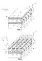
- a construction 10comprises an electrically insulative material 12 supporting a plurality of rails 14 - 18 .
- the railsare elongated along a direction of an illustrated axis 5 in the shown embodiment, and such axis may be referred to as a first axis.
- the railsare substantially straight in the shown embodiment, in other embodiments the rails may be curved or wavy. Even if the rails are curved or wavy, such rails may extend primarily along the illustrated axis 5 in some embodiments.
- the electrically insulative material 12may comprise any suitable composition or combination of compositions, and in some embodiments may comprise one or more of silicon nitride, silicon dioxide, and any of various doped glasses (for instance, borophosphosilicate glass, phosphosilicate glass, fluorosilicate glass, etc.).
- the insulative material 12may be supported over a semiconductor base (not shown). Such base may comprise, for example, monocrystalline silicon. If the electrically insulative material is supported by a semiconductor base, the combination of the electrically insulative material 12 and the underlying semiconductor base may be referred to as a semiconductor substrate, or as a portion of a semiconductor substrate.
- semiconductor substratemeans any construction comprising semiconductive material, including, but not limited to, bulk semiconductive materials such as a semiconductive wafer (either alone or in assemblies comprising other materials), and semiconductive material layers (either alone or in assemblies comprising other materials).
- substraterefers to any supporting structure, including, but not limited to, the semiconductor substrates described above.
- the insulative material 12may be over a semiconductor construction which comprises a semiconductor base and one or more levels of integrated circuitry.
- the levels of integrated circuitrymay comprise, for example, one or more of refractory metal materials, barrier materials, diffusion materials, insulator materials, etc.
- the rails 14 - 18may comprise several stacked materials in some embodiments.
- the bottom material of the shown railsis an electrically conductive material 20 .
- Such electrically conductive materialmay comprise any suitable composition or combination of compositions; and in some embodiments may comprise, consist essentially of, or consist of one or more of various metals (for instance, tungsten, titanium, copper, etc.), metal-containing substances (for instance, metal nitride, metal silicide, metal carbide, etc.) and conductively-doped semiconductor materials (for instance, conductively-doped silicon, conductively-doped germanium, etc.).
- the electrically conductive material 20forms electrically conductive lines 21 (only some of which are labeled) contained within the series of rails 14 - 18 .
- Such electrically conductive linesmay correspond to access/sense lines; and may, for example, correspond to wordlines or bitlines in some embodiments.
- the lines 21may be referred to as a first series of lines to distinguish them from another
- the individual rails 14 - 18comprise one or more materials over the lines 21 .
- the materials over lines 21are diagrammatically illustrated as regions 22 (only some of which are labeled) over the individual lines 21 .
- Uppermost portions of the regions 22comprise electrically conductive material 24 .
- the uppermost surface of material 24may ultimately correspond to the top of a bottom electrode of a memory cell. In other words, the uppermost surface of material 24 may be a region where a bottom electrode of a memory cell contacts memory cell material (described below); and thus material 24 may be referred to as bottom electrode contact material.
- Materials 20 and 24may or may not comprise the same composition as one another.
- materials 20 and 24may be the same conductive material as one another, and the intervening segment of region 22 may simply be more of the same conductive material.
- region 22may comprise one or more materials suitable for fabrication into select devices (for instance, transistors, diodes, etc.)—with an example of such other embodiments being described below with reference to FIGS. 8-12 .
- Each of the rails 14 - 18extends along multiple memory cell locations, with example memory cell locations 31 - 33 being labeled relative to the rail 14 .
- memory cellsmay be fabricated within such memory cell locations such that memory cell material of the memory cells is directly against the bottom electrode contact material 24 (as shown, for example, in FIG. 7 ).
- the rails 14 - 18may be formed with any suitable processing.
- the various materials of the rails 14 - 18may be formed across substrate 12 , and a patterned mask (not shown) may be formed over such materials to define locations of the rails 14 - 18 .
- a patternmay then be transferred from the mask into the materials of the rails with one or more suitable etches, and then the mask may be removed to leave the shown construction of FIG. 1 .
- the maskmay comprise any suitable composition or combination of compositions.
- the maskmay comprise photolithographically-patterned photoresist.
- the maskmay comprise one or more materials patterned utilizing pitch-multiplication methodologies.
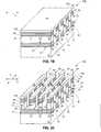
- FIG. 2shows dielectric material 36 formed within such gaps.
- the dielectric materialmay comprise any suitable composition or combination of compositions; and in some embodiments may comprise, consist essentially of or consist of silicon dioxide.
- the construction of FIG. 2is shown to have a planarized surface 37 extending across rails 14 - 18 , and across the dielectric material 36 .
- Such constructionmay be formed by initially forming dielectric material 36 to fill the gaps between the rails 14 - 18 , and to extend across upper surfaces of the rails; and then utilizing chemical-mechanical polishing (CMP) to remove the dielectric material from over the rails and form the planarized surface 37 .
- CMPchemical-mechanical polishing
- an expanse of pad material 38is formed across the planarized upper surface 37 , and an expanse of sacrificial material 40 is formed across the pad material.
- the pad materialmay comprise a sacrificial material provided as a buffer between the material 40 and the bottom electrode contact material 24 .
- the pad materialmay be omitted and the sacrificial material 40 may be provided directly on the bottom electrode contact material.
- the pad materialmay correspond to a memory cell material which is ultimately incorporated into memory cells.
- the memory cell materialmay be any material either now known, or yet to be developed, which is suitable for utilization in cross-point memory.
- the memory cell materialmay be a material suitable for utilization in one or more of PCRAM, RRAM, CBRAM, PCM, etc.
- the memory cell materialmay comprise an oxide containing one or more of aluminum, antimony, barium, calcium, cesium, germanium, hafnium, iron, lanthanum, lead, manganese, praseodymium, ruthenium, samarium, selenium, silicon, strontium, sulfur, tellurium, titanium, yttrium and zirconium.
- the memory cell materialmay comprise multivalent metal oxide; and may, for example, comprise, consist essentially of or consist of one or more of barium, ruthenium, strontium, titanium, calcium, manganese, praseodymium, lanthanum and samarium.
- the multivalent metal oxidemay comprise, consist essentially of, or consist of calcium manganese oxide doped with one or more of Pr, La, Sr and Sm.
- the memory cell materialmay comprise chalcogenide-type materials (for instance, materials comprising germanium in combination with one or more of antimony, tellurium, sulfur and selenium).
- the memory cell materialmay include additional layers, such as an ion source material suitable for contributing ions which ultimately form conductive bridges in PMC devices.
- the ion source materialmay comprise, for example, one or both of copper and silver; and may thus be configured for contributing copper cations and/or silver cations for formation of a conductive bridge.
- the ion source materialmay comprise a combination of copper and tellurium.
- the memory cell materialmay be a solid, gel, or any other suitable phase.
- the material 38may be alternatively either a sacrificial material or a memory cell material in some embodiments, the material 38 may be referred to herein as a pad material, sacrificial material, or memory cell material in describing various different embodiments.
- the term “pad material” as utilized in referring to material 38is generic relative to the terms “sacrificial material” and “memory cell material.”
- the sacrificial material 40may comprise any suitable composition or combination of compositions; and in some embodiments may comprise, consist essentially of, or consist of silicon (for instance, may consist of one or both of amorphous silicon and polycrystalline silicon).
- the sacrificial material 40is patterned into a series of lines 41 - 44 .
- the lines 41 - 44may be referred to as a second series of lines to distinguish them from the first series of lines corresponding to the lines 21 contained within the rails 14 - 18 .
- the lines 41 - 44cross the rails 14 - 18 ; and in the shown embodiment are substantially orthogonal to the rails 14 - 18 .
- the lines 41 - 44are elongated along an axis 7
- the rails 14 - 18are elongated along the axis 5 which is substantially orthogonal to the axis 7 .
- substantially orthogonalis utilized to indicate that the two axes are orthogonal within reasonable tolerances of design and measurement.
- the sacrificial material lines 41 - 44are directly over the memory cell locations (for instance, the locations 31 - 33 ).
- the pattern of the sacrificial material lines 41 - 44is transferred into the bottom electrode contact material 24 to singulate such material into segments 46 (only some of which are labeled). Each segment is associated with only a single memory cell location.
- the patternmay be transferred into the bottom electrode contact material with any suitable etch or combination of etches.
- the pattern of the sacrificial material linesis also transferred into the one or more materials beneath the bottom electrode contact material of the rails 14 - 18 .
- the singulation of regions 22 into pedestals 48may form individual select devices.
- FIGS. 8-12describe an embodiment in which the singulation forms individual diodes.
- the patternmay be transferred into the one or more materials of regions 22 with any suitable etch or combination of etches.
- the pedestals 48are capped with the bottom electrode contact material 24 , and are directly between the memory cell locations (for instance, the locations 31 - 33 ) and the conductive material 20 .
- the sacrificial material 40may be patterned into the lines 41 - 44 with any suitable processing.
- a patterned mask(not shown) may be formed over sacrificial material 40 to define locations of the lines 41 - 44 , a pattern may be transferred from the mask into material 40 with one or more suitable etches, and then the mask may be removed.
- the maskmay comprise any suitable composition or combination of compositions.
- the maskmay comprise photolithographically-patterned photoresist.
- the maskmay comprise one or more materials patterned utilizing pitch-multiplication methodologies. The mask may remain during the patterning of the materials of regions 22 in some embodiments, and may be removed prior to such patterning in other embodiments.
- the illustrated construction 10 at the processing stage of FIG. 4has a plurality of trenches 51 - 53 formed between the lines 41 - 44 .
- the trenches 51 - 53extend along the same direction as the lines 41 - 44 .
- the trenches 51 - 53may be referred to as a first series of trenches.
- dielectric material 54is formed within the trenches 51 - 53 . Although a single dielectric material is shown, in other embodiments multiple dielectric materials may be formed within such trenches. In some embodiments, the dielectric formed within the trenches 51 - 53 may comprise one or both of silicon nitride and silicon carbide.
- the material 54may be formed with any suitable processing, including, for example, one or more of atomic layer deposition (ALD), chemical vapor deposition (CVD) and physical vapor deposition (PVD). In some embodiments, material 54 may be formed to extend across upper surfaces of lines 41 - 44 , and may then be subjected to CMP to form the illustrated planarized upper surface 55 .
- ALDatomic layer deposition
- CVDchemical vapor deposition
- PVDphysical vapor deposition
- the material 54is deposited under conditions which leave voids 56 within trenches 51 - 53 .
- Suitable conditions for leaving such voidsare conditions in which the dielectric material pinches off across the tops of the trenches before uniformly filling central regions of the trenches.
- the dielectric provided within trenches 51 - 53have a low dielectric constant in that such can alleviate or prevent cross-talk that may otherwise occur between memory cells on opposing sides of the trenches.
- Airhas a low dielectric constant, and thus it can be advantageous to have the illustrated voids remaining within the trenches after formation of dielectric material 54 within such trenches.
- the dielectric within the trenches 51 - 53may be referred to as dielectric lines 60 - 62 .
- such dielectric linescomprise the illustrated voids 56 in combination with dielectric material 54 .
- the illustrated voids 56may consume at least about 10 percent of the volume of the dielectric lines formed within the trenches.
- voids 56are present in the shown embodiment, in other embodiments the dielectric 54 may be provided to entirely fill trenches 51 - 53 . Thus, the voids may be omitted.
- sacrificial material 40( FIG. 5 ) is removed to leave trenches 65 - 68 .
- the trenches 65 - 68may be referred to as a second series of trenches to distinguish them from the first series of trenches 51 - 53 ( FIG. 4 ).
- the sacrificial materialconsists of silicon (for instance, polycrystalline silicon), such may be removed utilizing tetramethylammonium hydroxide in some embodiments.
- trenches 65 - 68are directly over the bottom electrode contact material 24 .
- the formation of trenches 65 - 68exposes memory cell material 38 .
- material 38may correspond to a sacrificial pad material which is removed from over bottom electrode contact material 24 , and then replaced with memory cell material.
- material 38may be omitted (as discussed above with reference to FIG. 3 ); and in such embodiments the memory cell material may be formed subsequent to the formation of the trenches 65 - 68 to create the shown construction of FIG. 6 .
- the memory cell material 38 in the embodiment of FIG. 6is configured as a planar sheet. If the memory cell material is deposited after removal of sacrificial material 40 ( FIG. 5 ), the memory cell material may have a different configuration. For instance, FIG. 14 (discussed below) shows an embodiment in which memory cell material is configured as upwardly-opening container structures.
- the one or more memory cell materialsmay be any materials suitable for forming cross-point memory cells, either now known or later developed.
- the memory cell materialsmay be suitable for utilization in one or more of PCRAM, RRAM, CBRAM, PCM, etc.
- top electrode material 70is formed within the trenches 65 - 68 .
- the top electrode materialmay comprise any suitable composition or combination of compositions, and in some embodiments may comprise, consist essentially of, or consist of one or more of platinum, silver and copper. Accordingly, the top electrode material may comprise, consist essentially of, or consist of one or more noble metals. As discussed above in the “background” section of this disclosure, it can be difficult to pattern noble metals.
- the trenches 65 - 68enable utilization of a damascene process for patterning the electrode material 70 .
- top electrode material 70may be formed to fill trenches 65 - 68 and to extend over dielectric lines 60 - 62 .
- the top electrode materialmay then be planarized (for instance, subjected to CMP) to remove the top electrode material 70 from over the dielectric material lines and thereby form the illustrated top electrode lines 71 - 74 .
- Such top electrode linesextend along the axis 7 , and thus cross the bottom electrode lines 21 .
- the top electrode material 70may comprise copper.
- dielectric 54it may be desired for dielectric 54 to comprise copper barrier material, such as one or more nitrides and/or it may be desired for the conductive top electrode material to be surrounded by electrically conductive barrier material.
- Memory cells 76are formed in the memory cell locations (for instance, the locations 31 - 33 ), with such memory cells having memory cell material 38 directly between the bottom electrode contact material 24 and the electrode material 70 .
- the memory cellsmay be considered to be configured as a memory array.
- the formation of the top electrode lines 71 - 74may be considered to be replacement of at least some of the sacrificial material 40 of lines 41 - 44 ( FIG. 5 ) with top electrode material 70 .
- all of the sacrificial material 40 of lines 41 - 44is replaced with electrode material 70 .
- memory cell materialmay be formed within trenches 65 - 68 prior to formation of the electrode material 70 ; and in such embodiments a portion of the sacrificial material 40 of lines 41 - 44 may be considered to be replaced with the memory cell material, and another portion of the sacrificial material 40 of lines 41 - 44 may be considered to be replaced with the electrode material 70 .
- the materials of region 22may correspond to materials suitable for forming select devices.
- Example select devicesare transistors (for instance, vertical transistors) and diodes.
- FIGS. 8-12illustrate an example embodiment in which region 22 comprises materials suitable for fabrication into diodes.
- a construction 10 ais shown at a processing stage analogous to that of FIG. 1 .
- the rails 14 - 18comprise stacks of materials 20 , 78 and 80 .
- Such materialsmay correspond to suitable compositions for a diode construction.
- materials 20 , 78 and 80may be suitable compositions for a metal-silicon-metal diode (specifically, materials 20 and 80 may be metal, and material 78 may be silicon), or may be suitable compositions for a PIN diode (specifically, region 78 may be intrinsic semiconductor material, one of the regions 20 and 80 may be n-type doped semiconductor material, and the other of the regions 20 and 80 may be p-type doped semiconductor material).
- the bottom electrode contact material 24is shown to correspond to a top surface of material 80 .
- the bottom electrode contact materialmay be a separate conductive material from the material 80 of the diode compositions rather than being the shown top surface of material 80 .
- conductive line 20is shown to also be one of the diode compositions, in other embodiments the line may be a separate conductive material from the bottom diode composition.
- the diode compositions 20 , 78 and 80extend along the memory cell locations (for instance, the locations 31 - 33 ).
- construction 10 ais shown at a processing stage analogous to the above-discussed processing stage of FIG. 4 . Accordingly, the pad material 38 and sacrificial material 40 have been formed over rails 14 - 18 , and then the construction has been subjected to patterning to form the lines 41 - 44 and the trenches 51 - 53 .
- the formation of the trenchessingulates diodes 82 (only some of which are labeled) from the diode compositions 20 , 78 and 80 . Specifically, the trenches extend through materials 78 and 80 to form individual diodes under individual memory cell locations (for instance, the memory cell locations 31 - 33 ). In embodiments in which the bottom diode composition is a different conductive material from the material of the conductive line 20 , the trenches may extend through the bottom diode composition in addition to extending through the diode compositions 78 and 80 .
- construction 10 ais shown at a processing stage analogous to the above-discussed processing stage of FIG. 5 .
- the constructioncomprises the dielectric lines 60 - 62 within the trenches 51 - 53 .
- Such dielectric linescomprise the voids 56 in combination with the dielectric material 54 in the shown embodiment.
- the construction 10 aalso comprises the planarized upper surface 55 .
- construction 10 ais shown at a processing stage analogous to that discussed above with reference to FIG. 6 .
- the sacrificial material 40( FIG. 10 ) has been removed to leave the trenches 65 - 68 between the dielectric lines 60 - 62 .
- the material 38is at the bottoms of the trenches 65 - 68 , and corresponds to memory cell material of the type described above with reference to FIG. 6 .
- the material 38may be sacrificial material which is removed and replaced with memory cell material, as discussed above with reference to FIG. 6 .
- construction 10 ais shown at a processing stage analogous to that discussed above with reference to FIG. 7 .
- Top electrode material 70has been formed within the trenches 65 - 68 and patterned to form the top electrode lines 71 - 74 .
- Memory cells 76are formed in the memory cell locations (for instance, the locations 31 - 33 ), with such memory cells having memory cell material 38 directly between the bottom electrode contact material 24 and the electrode material 70 . Each memory cell is directly over one of the diodes 82 .
- FIGS. 8-12singulates the diodes 82 during patterning of the memory cell material 38 , which consolidates process steps relative to prior art processing. Such may improve throughput of a fabrication process relative to prior art processes, and may eliminate masking steps relative to prior art processes.
- FIGS. 13 and 14illustrate another example embodiment method.
- FIG. 13a construction 10 b is shown at a processing stage analogous to that described above with reference to FIG. 6 .
- the embodiment of FIG. 13does not have such pad material at the bottoms of such trenches.
- memory cell material 90is formed within the trenches 65 - 68 to line such trenches.
- the memory cell materialforms upwardly-opening container structures within the trenches.
- top electrode material 70is formed within such upwardly-opening container structures and patterned to form the top electrode lines 71 - 74 .
- the memory cell material 90may be formed as a planar structure rather than as the container-shaped structure of FIG. 14 .
- FIG. 15shows a construction 10 c at a processing stage analogous to that of FIG. 14 , but in which the memory cell material 90 has been formed as a planar structure.
- multiple memory cell materialsmay be utilized in the memory cells.
- the memory cell materialsmay have different shapes relative to one another.
- FIG. 16shows a construction 10 d utilizing two different memory cell materials 92 and 94 .
- the memory cell material 92is configured as a planar structure
- the memory cell material 94is configured as a container-shaped structure provided directly over and directly against the memory cell material 92 .
- the memory cell materials 92 and 94may be referred to as first and second memory cell materials, respectively.
- the memory cell material 92may correspond to the pad material 38 of FIG. 6 , and the material 94 may be provided within trenches 65 - 68 prior to forming the top electrode material 70 of FIG. 7 . In other embodiments, the memory cell materials 92 and 94 may both be formed within trenches 65 - 68 following a process stage analogous to that of FIG. 13 so that neither of the memory cell materials corresponds to the pad material 38 of FIG. 6 .
- the utilization of two memory cell materialsmay be useful in, for example, forming PCM cells in which one of the memory cell materials is an ion source (for instance, a combination of copper and tellurium) and the other is a switching region (for instance, an oxide or solid state electrolyte); forming RRAM cells in which one of the memory cell materials is a multivalent oxide and the other is a high k dielectric; etc.
- ion sourcefor instance, a combination of copper and tellurium
- a switching regionfor instance, an oxide or solid state electrolyte
- RRAM cellsin which one of the memory cell materials is a multivalent oxide and the other is a high k dielectric
- more than two memory cell materialsmay be utilized.
- a construction analogous to that of FIG. 16may be configured to have the electrode material 70 comprise copper, and the container-shaped material 94 may comprise a copper barrier material (such as a nitride). In such embodiments, the material 94 may or may not be a memory cell material.
- FIGS. 17-23illustrate another example embodiment method of fabricating an array of memory cells.
- a construction 10 eis shown at a processing stage analogous to that of FIG. 1 .
- the rails 14 - 18include memory cell material 38 and an electrically conductive material 100 .
- the material 100may comprise any suitable composition or combination of compositions, and in some embodiments may comprise one or more of various metals (for instance, tungsten, platinum, silver, copper, etc.), metal-containing compositions (for instance, metal silicide, metal carbide, etc.) and conductively-doped semiconductor materials (for instance, conductively-doped silicon, conductively-doped germanium, etc.).
- metalsfor instance, tungsten, platinum, silver, copper, etc.
- metal-containing compositionsfor instance, metal silicide, metal carbide, etc.
- conductively-doped semiconductor materialsfor instance, conductively-doped silicon, conductively-doped germanium, etc.
- FIGS. 18-23show the construction 10 e processed with methodology analogous to that discussed above with reference to FIGS. 2-7 to form an array of memory cells (with such array comprising the illustrated memory cells 31 - 33 in FIG. 23 ).
- the memory cell material 38 of FIGS. 17-23is singulated during the singulation of conductive material 24 .
- each of the memory cells in the memory array of FIG. 23(for instance, the memory cells 31 - 33 ) comprises a segment of material 38 , with each segment of material 38 being associated with only a single memory cell location.
- the memory cell material 38 within the memory array of FIG. 7is shown to be patterned into expanses which extended across multiple memory cells.
- the conductive material 100is patterned together with the memory cell material 38 to form segments of material 100 in one-to-one correspondence with the memory cells (for instance, the memory cells 31 - 33 ).
- region 22may correspond to materials suitable for forming select devices.
- Example select devicesare transistors (for instance, vertical transistors) and diodes.
- FIG. 24illustrates an example embodiment in which region 22 comprises materials suitable for fabrication into diodes. Specifically, FIG. 24 shows a construction 10 f at a processing stage analogous to that of FIG. 12 , with construction 10 f comprising the singulated memory cell material 38 and conductive material 100 discussed above with reference to FIGS. 17-23 .
- the regions 20 , 78 and 80may be regions of a diode (for instance, region 20 may be an n-type doped region, region 78 may be an intrinsic region, and region 80 may be a p-type doped region, as discussed above with reference to FIGS. 8-12 ).
- the memory cells 76also comprise a conductive material 102 between the top diode region 80 and the memory cell material 38 . Such conductive material may be utilized to improve adhesion between of material 38 , improve electrical transfer to material 38 and/or to improve other properties of the memory cells.
- the conductive material 102may comprise any suitable composition or combination of compositions and in some embodiments may comprise one or more of various metals (for instance, tungsten, platinum, silver, copper, etc.), metal-containing compositions (for instance, metal silicide, metal carbide, etc.) and conductively-doped semiconductor materials (for instance, conductively-doped silicon, conductively-doped germanium, etc.).
- the materials 100 and 102are shown to have different thicknesses relative to one another, with material 100 being thicker than material 102 . In other embodiments, materials 100 and 102 may be about the same thickness as one another, or material 102 may be thicker than material 100 .
- the memory cells and arrays discussed abovemay be incorporated into electronic systems.
- Such electronic systemsmay be any of a broad range of systems either now known or yet to be developed; with example electronic systems being clocks, televisions, cell phones, personal computers, automobiles, industrial control systems, aircraft, etc.
- Some embodimentsinclude a method of forming a plurality of memory cells.
- a series of railsis formed to extend along a first direction. Individual rails extend along multiple memory cell locations.
- the individual railscomprise bottom electrode contact material over electrically conductive lines.
- the electrically conductive linesare a first series of lines.
- An expanse of sacrificial materialis formed to extend across the rails.
- the sacrificial materialis patterned into a second series of lines that extends along a second direction that crosses the first direction.
- a pattern of the second series of linesis transferred into the bottom electrode contact material to singulate the bottom electrode contact material into segments associated with only single memory cell locations. At least a portion of the sacrificial material of the second series of lines is replaced with top electrode material.
- Some embodimentsinclude a method of forming a plurality of memory cells.
- a series of railsis formed to extend along a first direction. Individual rails extend along multiple memory cell locations. The individual rails comprise bottom electrode contact material stacked over electrically conductive lines.
- a series of sacrificial material linesis formed to extend along a second direction that crosses the first direction. The sacrificial material lines are directly over the memory cell locations. A pattern of the sacrificial material lines is transferred into the bottom electrode contact material to singulate the bottom electrode contact material into segments associated with only single memory cell locations.
- a series of dielectric linesis formed between the sacrificial material lines. The dielectric lines extend along the second direction. The sacrificial material lines are removed to leave trenches between the dielectric lines.
- top electrode materialis formed within the trenches and over the dielectric material lines.
- the top electrode materialis planarized to remove the top electrode material from over the dielectric material lines and thereby form a plurality of top electrode lines directly over the memory cell locations.
- the top electrode linesextend along the second direction.
- Some embodimentsinclude a method of forming a plurality of memory cells.
- a series of railsis formed to extend along a first direction. Individual rails extend along multiple memory cell locations.
- the individual railscomprise bottom electrode contact material stacked over electrically conductive lines.
- the electrically conductive linesare a first series of lines.
- An expanse of sacrificial materialis formed to extend across the rails.
- the sacrificial materialis patterned into a second series of lines which extend along a second direction that crosses the first direction.
- a pattern of the second series of linesis transferred into the bottom electrode contact material to singulate the bottom electrode contact material into segments associated with only single memory cell locations. The transferring of the pattern forms a series of first trenches that extend along the second direction.
- Individual trenches of the first seriesare between adjacent lines of the second series.
- One or more dielectric materialsare formed within the first series of trenches. After said one or more dielectric materials are formed, the sacrificial material is removed to leave a second series of trenches that extend along the second direction. Individual trenches of the second series are directly over the segments of bottom electrode contact material.
- Top electrode materialis formed within the second series of trenches and over the one or more dielectric materials. The top electrode material is planarized to remove the top electrode material from over the one or more dielectric materials and thereby form a plurality of top electrode lines that extend along the second direction.
- Some embodimentsinclude a memory array that comprises a first series of electrically conductive lines extending along a first direction. Pillars are over the first series of electrically conductive lines. The pillars are capped with bottom electrode contact material and are directly between the electrically conductive lines of the first series and memory cell locations. One or more memory cell materials are over the pillars and within the memory cell locations. A second series of electrically conductive lines extends along a second direction that crosses the first direction. The second series of electrically conductive lines comprises top electrode material. The memory cell locations are directly between the electrically conductive lines of the first and second series, and are in regions where the electrically conductive lines of the second series overlap the electrically conductive lines of the first series. The electrically conductive lines of the second series comprise one or more of platinum, copper and silver.
- Some embodimentsinclude a memory array that comprises a first series of electrically conductive lines extending along a first direction. Pillars are over the first series of electrically conductive lines. The pillars are capped with bottom electrode contact material and are directly between the electrically conductive lines of the first series and memory cell locations. A first memory cell material is over the pillars and within the memory cell locations. The first memory cell material is a planar sheet within the memory cell locations, and is directly against the bottom electrode contact material. A second memory cell material is over the first memory cell material. The second memory cell material is configured as a plurality of upwardly-opening containers that extend linearly along a second direction that crosses the first direction. A second series of electrically conductive lines is within the containers. The second series of electrically conductive lines comprises top electrode material. The memory cell locations are directly between the electrically conductive lines of the first and second series, and are in regions where the electrically conductive lines of the second series overlap the electrically conductive lines of the first series.
Landscapes
- Semiconductor Memories (AREA)
Abstract
Description
- Memory arrays and methods of forming memory cells.
- Memory is one type of integrated circuitry, and is used in computer systems for storing data. Integrated memory is usually fabricated in one or more arrays of individual memory cells. The memory cells are configured to retain or store memory in at least two different selectable states. In a binary system, the states are considered as either a “0” or a “1”. In other systems, at least some individual memory cells may be configured to store more than two levels or states of information.
- Integrated circuit fabrication continues to strive to produce smaller and denser integrated circuits. Accordingly, there has been substantial interest in memory cells that can be utilized in cross-point architectures. Example types of memory cells that are suitable for utilization in cross-point architectures are resistive RAM (RRAM) cells, phase change RAM (PCRAM) cells, and programmable metallization cells (PMCs)—which may be alternatively referred to as a conductive bridging RAM (CBRAM) cells, nanobridge memory cells, or electrolyte memory cells. The memory cell types are not mutually exclusive. For example, RRAM may be considered to encompass PCRAM and PMCs.
- The cross-point architectures may comprise memory cell material between a pair of electrodes. Various problems can be encountered in the development of such architectures. The problems can involve, for example, mask misalignment during the various patterning steps utilized to pattern the electrodes and the memory cell material. Each electrode may be patterned with a separate masking step, and the memory cell material may be patterned with yet another masking step. Thus, there can be at least three masking steps to align during the fabrication of the memory cells. As another example, the problems may involve difficulties in utilizing some types of memory cell materials. For instance, some memory cell materials comprise oxides which are reactive toward many conductive materials. Thus it can be desired to use noble metals (for instance, platinum, silver, etc.) in electrodes that contact such oxides. However, the non-reactivity of the noble metals can make them difficult to pattern.
- It would be desirable to develop improvements in memory cell fabrication which alleviate one or more of the above-discussed problems, and to develop improved memory cells.
FIGS. 1-7 are diagrammatic three-dimensional views of a portion of a construction shown at various process stages of an example embodiment method of fabricating memory cells.FIGS. 8-12 are diagrammatic three-dimensional views of a portion of a construction shown at various process stages of another example embodiment method of fabricating memory cells.FIGS. 13 and 14 are diagrammatic three-dimensional views of a portion of a construction shown at various process stages of another example embodiment method of fabricating memory cells.FIG. 15 is a diagrammatic three-dimensional view of a portion of a construction shown at a process stage of another example embodiment method of fabricating memory cells.FIG. 16 is a diagrammatic three-dimensional view of a portion of a construction shown at a process stage of another example embodiment method of fabricating memory cells.FIGS. 17-23 are diagrammatic three-dimensional views of a portion of a construction shown at various process stages of another example embodiment method of fabricating memory cells.FIG. 24 is a diagrammatic three-dimensional view of a portion of a construction shown at a process stage of another example embodiment method of fabricating memory cells.- In some embodiments, the invention includes a two-mask, damascene scheme that may be utilized for forming cross-point memory. In some embodiments, the scheme may be utilized for patterning select devices (for instance, diodes, transistors, etc.) in addition to memory cells; and in some embodiments the scheme may be utilized for patterning memory cells separate from select devices. The scheme may be utilized for patterning noble metals, and may be utilized in combination with pitch-multiplication technologies. In some embodiments, the scheme may be utilized for forming highly integrated memory; such as, for example, memory having feature sizes of less than or equal to about 20 nanometers.
- Example embodiments are described with reference to
FIGS. 1-24 . - Referring to
FIG. 1 , aconstruction 10 comprises an electricallyinsulative material 12 supporting a plurality of rails14-18. The rails are elongated along a direction of an illustratedaxis 5 in the shown embodiment, and such axis may be referred to as a first axis. Although the rails are substantially straight in the shown embodiment, in other embodiments the rails may be curved or wavy. Even if the rails are curved or wavy, such rails may extend primarily along the illustratedaxis 5 in some embodiments. - The
electrically insulative material 12 may comprise any suitable composition or combination of compositions, and in some embodiments may comprise one or more of silicon nitride, silicon dioxide, and any of various doped glasses (for instance, borophosphosilicate glass, phosphosilicate glass, fluorosilicate glass, etc.). Theinsulative material 12 may be supported over a semiconductor base (not shown). Such base may comprise, for example, monocrystalline silicon. If the electrically insulative material is supported by a semiconductor base, the combination of theelectrically insulative material 12 and the underlying semiconductor base may be referred to as a semiconductor substrate, or as a portion of a semiconductor substrate. The terms “semiconductive substrate,” “semiconductor construction” and “semiconductor substrate” mean any construction comprising semiconductive material, including, but not limited to, bulk semiconductive materials such as a semiconductive wafer (either alone or in assemblies comprising other materials), and semiconductive material layers (either alone or in assemblies comprising other materials). The term “substrate” refers to any supporting structure, including, but not limited to, the semiconductor substrates described above. In some embodiments, theinsulative material 12 may be over a semiconductor construction which comprises a semiconductor base and one or more levels of integrated circuitry. In such embodiments, the levels of integrated circuitry may comprise, for example, one or more of refractory metal materials, barrier materials, diffusion materials, insulator materials, etc. - The rails14-18 may comprise several stacked materials in some embodiments. The bottom material of the shown rails is an electrically
conductive material 20. Such electrically conductive material may comprise any suitable composition or combination of compositions; and in some embodiments may comprise, consist essentially of, or consist of one or more of various metals (for instance, tungsten, titanium, copper, etc.), metal-containing substances (for instance, metal nitride, metal silicide, metal carbide, etc.) and conductively-doped semiconductor materials (for instance, conductively-doped silicon, conductively-doped germanium, etc.). The electricallyconductive material 20 forms electrically conductive lines21 (only some of which are labeled) contained within the series of rails14-18. Such electrically conductive lines may correspond to access/sense lines; and may, for example, correspond to wordlines or bitlines in some embodiments. Thelines 21 may be referred to as a first series of lines to distinguish them from another series of lines formed in subsequent processing. - The individual rails14-18 comprise one or more materials over the
lines 21. The materials overlines 21 are diagrammatically illustrated as regions22 (only some of which are labeled) over theindividual lines 21. Uppermost portions of theregions 22 comprise electricallyconductive material 24. The uppermost surface ofmaterial 24 may ultimately correspond to the top of a bottom electrode of a memory cell. In other words, the uppermost surface ofmaterial 24 may be a region where a bottom electrode of a memory cell contacts memory cell material (described below); and thusmaterial 24 may be referred to as bottom electrode contact material. Materials materials region 22 may simply be more of the same conductive material. In other embodiments,region 22 may comprise one or more materials suitable for fabrication into select devices (for instance, transistors, diodes, etc.)—with an example of such other embodiments being described below with reference toFIGS. 8-12 .- Each of the rails14-18 extends along multiple memory cell locations, with example memory cell locations31-33 being labeled relative to the
rail 14. Ultimately, memory cells may be fabricated within such memory cell locations such that memory cell material of the memory cells is directly against the bottom electrode contact material24 (as shown, for example, inFIG. 7 ). - The rails14-18 may be formed with any suitable processing. For instance, the various materials of the rails14-18 may be formed across
substrate 12, and a patterned mask (not shown) may be formed over such materials to define locations of the rails14-18. A pattern may then be transferred from the mask into the materials of the rails with one or more suitable etches, and then the mask may be removed to leave the shown construction ofFIG. 1 . The mask may comprise any suitable composition or combination of compositions. For instance, the mask may comprise photolithographically-patterned photoresist. As another example, the mask may comprise one or more materials patterned utilizing pitch-multiplication methodologies. - In the shown embodiment of
FIG. 1 , the rails14-18 are spaced from one another by intervening gaps.FIG. 2 showsdielectric material 36 formed within such gaps. The dielectric material may comprise any suitable composition or combination of compositions; and in some embodiments may comprise, consist essentially of or consist of silicon dioxide. The construction ofFIG. 2 is shown to have aplanarized surface 37 extending across rails14-18, and across thedielectric material 36. Such construction may be formed by initially formingdielectric material 36 to fill the gaps between the rails14-18, and to extend across upper surfaces of the rails; and then utilizing chemical-mechanical polishing (CMP) to remove the dielectric material from over the rails and form theplanarized surface 37. - Referring to
FIG. 3 , an expanse ofpad material 38 is formed across the planarizedupper surface 37, and an expanse ofsacrificial material 40 is formed across the pad material. - In some embodiments, the pad material may comprise a sacrificial material provided as a buffer between the material40 and the bottom
electrode contact material 24. In some embodiments, the pad material may be omitted and thesacrificial material 40 may be provided directly on the bottom electrode contact material. In some embodiments, the pad material may correspond to a memory cell material which is ultimately incorporated into memory cells. The memory cell material may be any material either now known, or yet to be developed, which is suitable for utilization in cross-point memory. For instance, the memory cell material may be a material suitable for utilization in one or more of PCRAM, RRAM, CBRAM, PCM, etc. In some embodiments, the memory cell material may comprise an oxide containing one or more of aluminum, antimony, barium, calcium, cesium, germanium, hafnium, iron, lanthanum, lead, manganese, praseodymium, ruthenium, samarium, selenium, silicon, strontium, sulfur, tellurium, titanium, yttrium and zirconium. In some embodiments, the memory cell material may comprise multivalent metal oxide; and may, for example, comprise, consist essentially of or consist of one or more of barium, ruthenium, strontium, titanium, calcium, manganese, praseodymium, lanthanum and samarium. For instance, the multivalent metal oxide may comprise, consist essentially of, or consist of calcium manganese oxide doped with one or more of Pr, La, Sr and Sm. In some embodiments, the memory cell material may comprise chalcogenide-type materials (for instance, materials comprising germanium in combination with one or more of antimony, tellurium, sulfur and selenium). In some embodiments, the memory cell material may include additional layers, such as an ion source material suitable for contributing ions which ultimately form conductive bridges in PMC devices. The ion source material may comprise, for example, one or both of copper and silver; and may thus be configured for contributing copper cations and/or silver cations for formation of a conductive bridge. For instance, the ion source material may comprise a combination of copper and tellurium. The memory cell material may be a solid, gel, or any other suitable phase. - Since the
material 38 may be alternatively either a sacrificial material or a memory cell material in some embodiments, thematerial 38 may be referred to herein as a pad material, sacrificial material, or memory cell material in describing various different embodiments. The term “pad material” as utilized in referring tomaterial 38 is generic relative to the terms “sacrificial material” and “memory cell material.” - The
sacrificial material 40 may comprise any suitable composition or combination of compositions; and in some embodiments may comprise, consist essentially of, or consist of silicon (for instance, may consist of one or both of amorphous silicon and polycrystalline silicon). - Referring to
FIG. 4 , thesacrificial material 40 is patterned into a series of lines41-44. The lines41-44 may be referred to as a second series of lines to distinguish them from the first series of lines corresponding to thelines 21 contained within the rails14-18. The lines41-44 cross the rails14-18; and in the shown embodiment are substantially orthogonal to the rails14-18. Specifically, the lines41-44 are elongated along anaxis 7, and the rails14-18 are elongated along theaxis 5 which is substantially orthogonal to theaxis 7. The term “substantially orthogonal” is utilized to indicate that the two axes are orthogonal within reasonable tolerances of design and measurement. - The sacrificial material lines41-44 are directly over the memory cell locations (for instance, the locations31-33). The pattern of the sacrificial material lines41-44 is transferred into the bottom
electrode contact material 24 to singulate such material into segments46 (only some of which are labeled). Each segment is associated with only a single memory cell location. The pattern may be transferred into the bottom electrode contact material with any suitable etch or combination of etches. - The pattern of the sacrificial material lines is also transferred into the one or more materials beneath the bottom electrode contact material of the rails14-18. Such singulates the
regions 22 into pedestals (or pillars)48 (only some of which are labeled). In embodiments in which theregions 22 comprise materials suitable for incorporation into select devices, the singulation ofregions 22 intopedestals 48 may form individual select devices. For instance,FIGS. 8-12 describe an embodiment in which the singulation forms individual diodes. The pattern may be transferred into the one or more materials ofregions 22 with any suitable etch or combination of etches. Thepedestals 48 are capped with the bottomelectrode contact material 24, and are directly between the memory cell locations (for instance, the locations31-33) and theconductive material 20. - The
sacrificial material 40 may be patterned into the lines41-44 with any suitable processing. For instance, a patterned mask (not shown) may be formed oversacrificial material 40 to define locations of the lines41-44, a pattern may be transferred from the mask intomaterial 40 with one or more suitable etches, and then the mask may be removed. The mask may comprise any suitable composition or combination of compositions. For instance, the mask may comprise photolithographically-patterned photoresist. As another example, the mask may comprise one or more materials patterned utilizing pitch-multiplication methodologies. The mask may remain during the patterning of the materials ofregions 22 in some embodiments, and may be removed prior to such patterning in other embodiments. - The illustrated
construction 10 at the processing stage ofFIG. 4 has a plurality of trenches51-53 formed between the lines41-44. The trenches51-53 extend along the same direction as the lines41-44. In some embodiments, the trenches51-53 may be referred to as a first series of trenches. - Referring to
FIG. 5 ,dielectric material 54 is formed within the trenches51-53. Although a single dielectric material is shown, in other embodiments multiple dielectric materials may be formed within such trenches. In some embodiments, the dielectric formed within the trenches51-53 may comprise one or both of silicon nitride and silicon carbide. Thematerial 54 may be formed with any suitable processing, including, for example, one or more of atomic layer deposition (ALD), chemical vapor deposition (CVD) and physical vapor deposition (PVD). In some embodiments,material 54 may be formed to extend across upper surfaces of lines41-44, and may then be subjected to CMP to form the illustrated planarizedupper surface 55. - In the shown embodiment, the
material 54 is deposited under conditions which leavevoids 56 within trenches51-53. Suitable conditions for leaving such voids are conditions in which the dielectric material pinches off across the tops of the trenches before uniformly filling central regions of the trenches. It can be advantageous that the dielectric provided within trenches51-53 have a low dielectric constant in that such can alleviate or prevent cross-talk that may otherwise occur between memory cells on opposing sides of the trenches. Air has a low dielectric constant, and thus it can be advantageous to have the illustrated voids remaining within the trenches after formation ofdielectric material 54 within such trenches. - In some embodiments, the dielectric within the trenches51-53 may be referred to as dielectric lines60-62. In the shown embodiment, such dielectric lines comprise the illustrated
voids 56 in combination withdielectric material 54. In some embodiments, the illustratedvoids 56 may consume at least about10 percent of the volume of the dielectric lines formed within the trenches. - Although
voids 56 are present in the shown embodiment, in other embodiments the dielectric54 may be provided to entirely fill trenches51-53. Thus, the voids may be omitted. - Referring to
FIG. 6 , sacrificial material40 (FIG. 5 ) is removed to leave trenches65-68. The trenches65-68 may be referred to as a second series of trenches to distinguish them from the first series of trenches51-53 (FIG. 4 ). If the sacrificial material consists of silicon (for instance, polycrystalline silicon), such may be removed utilizing tetramethylammonium hydroxide in some embodiments. - The trenches65-68 are directly over the bottom
electrode contact material 24. In the shown embodiment, the formation of trenches65-68 exposesmemory cell material 38. In other embodiments,material 38 may correspond to a sacrificial pad material which is removed from over bottomelectrode contact material 24, and then replaced with memory cell material. In yet other embodiments,material 38 may be omitted (as discussed above with reference toFIG. 3 ); and in such embodiments the memory cell material may be formed subsequent to the formation of the trenches65-68 to create the shown construction ofFIG. 6 . - The
memory cell material 38 in the embodiment ofFIG. 6 is configured as a planar sheet. If the memory cell material is deposited after removal of sacrificial material40 (FIG. 5 ), the memory cell material may have a different configuration. For instance,FIG. 14 (discussed below) shows an embodiment in which memory cell material is configured as upwardly-opening container structures. - Although only the single
memory cell material 38 is shown in the embodiment ofFIG. 6 , in other embodiments multiple memory cell materials may be utilized. The one or more memory cell materials may be any materials suitable for forming cross-point memory cells, either now known or later developed. For instance, the memory cell materials may be suitable for utilization in one or more of PCRAM, RRAM, CBRAM, PCM, etc. - Referring to
FIG. 7 ,top electrode material 70 is formed within the trenches65-68. The top electrode material may comprise any suitable composition or combination of compositions, and in some embodiments may comprise, consist essentially of, or consist of one or more of platinum, silver and copper. Accordingly, the top electrode material may comprise, consist essentially of, or consist of one or more noble metals. As discussed above in the “background” section of this disclosure, it can be difficult to pattern noble metals. However, in some embodiments the trenches65-68 enable utilization of a damascene process for patterning theelectrode material 70. Specifically,top electrode material 70 may be formed to fill trenches65-68 and to extend over dielectric lines60-62. The top electrode material may then be planarized (for instance, subjected to CMP) to remove thetop electrode material 70 from over the dielectric material lines and thereby form the illustrated top electrode lines71-74. Such top electrode lines extend along theaxis 7, and thus cross the bottom electrode lines21. - In some embodiments, the
top electrode material 70 may comprise copper. In such embodiments, it may be desired for dielectric54 to comprise copper barrier material, such as one or more nitrides and/or it may be desired for the conductive top electrode material to be surrounded by electrically conductive barrier material. - Memory cells76 (only some of which are labeled) are formed in the memory cell locations (for instance, the locations31-33), with such memory cells having
memory cell material 38 directly between the bottomelectrode contact material 24 and theelectrode material 70. The memory cells may be considered to be configured as a memory array. - In some embodiments, the formation of the top electrode lines71-74 may be considered to be replacement of at least some of the
sacrificial material 40 of lines41-44 (FIG. 5 ) withtop electrode material 70. In the shown embodiment, all of thesacrificial material 40 of lines41-44 is replaced withelectrode material 70. In some embodiments, memory cell material may be formed within trenches65-68 prior to formation of theelectrode material 70; and in such embodiments a portion of thesacrificial material 40 of lines41-44 may be considered to be replaced with the memory cell material, and another portion of thesacrificial material 40 of lines41-44 may be considered to be replaced with theelectrode material 70. - As discussed above, in some embodiments the materials of region22 (
FIG. 1 ) may correspond to materials suitable for forming select devices. Example select devices are transistors (for instance, vertical transistors) and diodes.FIGS. 8-12 illustrate an example embodiment in whichregion 22 comprises materials suitable for fabrication into diodes. - Referring to
FIG. 8 , aconstruction 10ais shown at a processing stage analogous to that ofFIG. 1 . The rails14-18 comprise stacks ofmaterials materials materials material 78 may be silicon), or may be suitable compositions for a PIN diode (specifically,region 78 may be intrinsic semiconductor material, one of theregions regions electrode contact material 24 is shown to correspond to a top surface ofmaterial 80. In some embodiments, the bottom electrode contact material may be a separate conductive material from thematerial 80 of the diode compositions rather than being the shown top surface ofmaterial 80. Also, althoughconductive line 20 is shown to also be one of the diode compositions, in other embodiments the line may be a separate conductive material from the bottom diode composition. - The
diode compositions - Referring to
FIG. 9 ,construction 10ais shown at a processing stage analogous to the above-discussed processing stage ofFIG. 4 . Accordingly, thepad material 38 andsacrificial material 40 have been formed over rails14-18, and then the construction has been subjected to patterning to form the lines41-44 and the trenches51-53. The formation of the trenches singulates diodes82 (only some of which are labeled) from thediode compositions materials conductive line 20, the trenches may extend through the bottom diode composition in addition to extending through thediode compositions - Referring to
FIG. 10 ,construction 10ais shown at a processing stage analogous to the above-discussed processing stage ofFIG. 5 . The construction comprises the dielectric lines60-62 within the trenches51-53. Such dielectric lines comprise thevoids 56 in combination with thedielectric material 54 in the shown embodiment. Theconstruction 10aalso comprises the planarizedupper surface 55. - Referring to
FIG. 11 ,construction 10ais shown at a processing stage analogous to that discussed above with reference toFIG. 6 . The sacrificial material40 (FIG. 10 ) has been removed to leave the trenches65-68 between the dielectric lines60-62. Thematerial 38 is at the bottoms of the trenches65-68, and corresponds to memory cell material of the type described above with reference toFIG. 6 . In other embodiments, thematerial 38 may be sacrificial material which is removed and replaced with memory cell material, as discussed above with reference toFIG. 6 . - Referring to
FIG. 12 ,construction 10ais shown at a processing stage analogous to that discussed above with reference toFIG. 7 .Top electrode material 70 has been formed within the trenches65-68 and patterned to form the top electrode lines71-74. - Memory cells76 (only some of which are labeled) are formed in the memory cell locations (for instance, the locations31-33), with such memory cells having
memory cell material 38 directly between the bottomelectrode contact material 24 and theelectrode material 70. Each memory cell is directly over one of thediodes 82. - The embodiment of
FIGS. 8-12 singulates thediodes 82 during patterning of thememory cell material 38, which consolidates process steps relative to prior art processing. Such may improve throughput of a fabrication process relative to prior art processes, and may eliminate masking steps relative to prior art processes. FIGS. 13 and 14 illustrate another example embodiment method.- Referring to
FIG. 13 , aconstruction 10bis shown at a processing stage analogous to that described above with reference toFIG. 6 . However, unlike the embodiment ofFIG. 6 which had thepad material 38 at the bottoms of the trenches65-68, the embodiment ofFIG. 13 does not have such pad material at the bottoms of such trenches. - Referring to
FIG. 14 ,memory cell material 90 is formed within the trenches65-68 to line such trenches. The memory cell material forms upwardly-opening container structures within the trenches. Subsequently,top electrode material 70 is formed within such upwardly-opening container structures and patterned to form the top electrode lines71-74. - In some embodiments, the
memory cell material 90 may be formed as a planar structure rather than as the container-shaped structure ofFIG. 14 . For instance,FIG. 15 shows aconstruction 10cat a processing stage analogous to that ofFIG. 14 , but in which thememory cell material 90 has been formed as a planar structure. - In some embodiments, multiple memory cell materials may be utilized in the memory cells. In such embodiments, the memory cell materials may have different shapes relative to one another. For instance,
FIG. 16 shows aconstruction 10dutilizing two differentmemory cell materials memory cell material 92 is configured as a planar structure, and thememory cell material 94 is configured as a container-shaped structure provided directly over and directly against thememory cell material 92. Thememory cell materials - In some embodiments, the
memory cell material 92 may correspond to thepad material 38 ofFIG. 6 , and thematerial 94 may be provided within trenches65-68 prior to forming thetop electrode material 70 ofFIG. 7 . In other embodiments, thememory cell materials FIG. 13 so that neither of the memory cell materials corresponds to thepad material 38 ofFIG. 6 . - The utilization of two memory cell materials may be useful in, for example, forming PCM cells in which one of the memory cell materials is an ion source (for instance, a combination of copper and tellurium) and the other is a switching region (for instance, an oxide or solid state electrolyte); forming RRAM cells in which one of the memory cell materials is a multivalent oxide and the other is a high k dielectric; etc. In some embodiments, more than two memory cell materials may be utilized.
- In some embodiments, a construction analogous to that of
FIG. 16 may be configured to have theelectrode material 70 comprise copper, and the container-shapedmaterial 94 may comprise a copper barrier material (such as a nitride). In such embodiments, thematerial 94 may or may not be a memory cell material. FIGS. 17-23 illustrate another example embodiment method of fabricating an array of memory cells. Referring toFIG. 17 , aconstruction 10eis shown at a processing stage analogous to that ofFIG. 1 . However, unlike the construction ofFIG. 1 , the rails14-18 includememory cell material 38 and an electricallyconductive material 100. Thematerial 100 may comprise any suitable composition or combination of compositions, and in some embodiments may comprise one or more of various metals (for instance, tungsten, platinum, silver, copper, etc.), metal-containing compositions (for instance, metal silicide, metal carbide, etc.) and conductively-doped semiconductor materials (for instance, conductively-doped silicon, conductively-doped germanium, etc.). Although only one memory cell material is shown, in other embodiments multiple memory cells may be provided betweenconductive materials FIGS. 18-23 show theconstruction 10eprocessed with methodology analogous to that discussed above with reference toFIGS. 2-7 to form an array of memory cells (with such array comprising the illustrated memory cells31-33 inFIG. 23 ). Thememory cell material 38 ofFIGS. 17-23 is singulated during the singulation ofconductive material 24. Accordingly, each of the memory cells in the memory array ofFIG. 23 (for instance, the memory cells31-33) comprises a segment ofmaterial 38, with each segment ofmaterial 38 being associated with only a single memory cell location. In contrast, thememory cell material 38 within the memory array ofFIG. 7 is shown to be patterned into expanses which extended across multiple memory cells. In the shown embodiment ofFIGS. 17-23 , theconductive material 100 is patterned together with thememory cell material 38 to form segments ofmaterial 100 in one-to-one correspondence with the memory cells (for instance, the memory cells31-33).- The materials of region22 (
FIGS. 17-23 ) may correspond to materials suitable for forming select devices. Example select devices are transistors (for instance, vertical transistors) and diodes.FIG. 24 illustrates an example embodiment in whichregion 22 comprises materials suitable for fabrication into diodes. Specifically,FIG. 24 shows aconstruction 10fat a processing stage analogous to that ofFIG. 12 , withconstruction 10fcomprising the singulatedmemory cell material 38 andconductive material 100 discussed above with reference toFIGS. 17-23 . Theregions region 20 may be an n-type doped region,region 78 may be an intrinsic region, andregion 80 may be a p-type doped region, as discussed above with reference toFIGS. 8-12 ). In the shown embodiment, thememory cells 76 also comprise aconductive material 102 between thetop diode region 80 and thememory cell material 38. Such conductive material may be utilized to improve adhesion between ofmaterial 38, improve electrical transfer tomaterial 38 and/or to improve other properties of the memory cells. Theconductive material 102 may comprise any suitable composition or combination of compositions and in some embodiments may comprise one or more of various metals (for instance, tungsten, platinum, silver, copper, etc.), metal-containing compositions (for instance, metal silicide, metal carbide, etc.) and conductively-doped semiconductor materials (for instance, conductively-doped silicon, conductively-doped germanium, etc.). Thematerials material 100 being thicker thanmaterial 102. In other embodiments,materials material 102 may be thicker thanmaterial 100. - The memory cells and arrays discussed above may be incorporated into electronic systems. Such electronic systems may be any of a broad range of systems either now known or yet to be developed; with example electronic systems being clocks, televisions, cell phones, personal computers, automobiles, industrial control systems, aircraft, etc.
- The particular orientation of the various embodiments in the drawings is for illustrative purposes only, and the embodiments may be rotated relative to the shown orientations in some applications. The description provided herein, and the claims that follow, pertain to any structures that have the described relationships between various features, regardless of whether the structures are in the particular orientation of the drawings, or are rotated relative to such orientation.
- The cross-sectional views of the accompanying illustrations only show features within the planes of the cross-sections, and do not show materials behind the planes of the cross-sections in order to simplify the drawings.
- When a structure is referred to above as being “on” or “against” another structure, it can be directly on the other structure or intervening structures may also be present. In contrast, when a structure is referred to as being “directly on” or “directly against” another structure, there are no intervening structures present. When a structure is referred to as being “connected” or “coupled” to another structure, it can be directly connected or coupled to the other structure, or intervening structures may be present. In contrast, when a structure is referred to as being “directly connected” or “directly coupled” to another structure, there are no intervening structures present.
- Some embodiments include a method of forming a plurality of memory cells. A series of rails is formed to extend along a first direction. Individual rails extend along multiple memory cell locations. The individual rails comprise bottom electrode contact material over electrically conductive lines. The electrically conductive lines are a first series of lines. An expanse of sacrificial material is formed to extend across the rails. The sacrificial material is patterned into a second series of lines that extends along a second direction that crosses the first direction. A pattern of the second series of lines is transferred into the bottom electrode contact material to singulate the bottom electrode contact material into segments associated with only single memory cell locations. At least a portion of the sacrificial material of the second series of lines is replaced with top electrode material.
- Some embodiments include a method of forming a plurality of memory cells. A series of rails is formed to extend along a first direction. Individual rails extend along multiple memory cell locations. The individual rails comprise bottom electrode contact material stacked over electrically conductive lines. A series of sacrificial material lines is formed to extend along a second direction that crosses the first direction. The sacrificial material lines are directly over the memory cell locations. A pattern of the sacrificial material lines is transferred into the bottom electrode contact material to singulate the bottom electrode contact material into segments associated with only single memory cell locations. A series of dielectric lines is formed between the sacrificial material lines. The dielectric lines extend along the second direction. The sacrificial material lines are removed to leave trenches between the dielectric lines. The trenches are directly over the segments of the bottom electrode contact material. Top electrode material is formed within the trenches and over the dielectric material lines. The top electrode material is planarized to remove the top electrode material from over the dielectric material lines and thereby form a plurality of top electrode lines directly over the memory cell locations. The top electrode lines extend along the second direction.
- Some embodiments include a method of forming a plurality of memory cells. A series of rails is formed to extend along a first direction. Individual rails extend along multiple memory cell locations. The individual rails comprise bottom electrode contact material stacked over electrically conductive lines. The electrically conductive lines are a first series of lines. An expanse of sacrificial material is formed to extend across the rails. The sacrificial material is patterned into a second series of lines which extend along a second direction that crosses the first direction. A pattern of the second series of lines is transferred into the bottom electrode contact material to singulate the bottom electrode contact material into segments associated with only single memory cell locations. The transferring of the pattern forms a series of first trenches that extend along the second direction. Individual trenches of the first series are between adjacent lines of the second series. One or more dielectric materials are formed within the first series of trenches. After said one or more dielectric materials are formed, the sacrificial material is removed to leave a second series of trenches that extend along the second direction. Individual trenches of the second series are directly over the segments of bottom electrode contact material. Top electrode material is formed within the second series of trenches and over the one or more dielectric materials. The top electrode material is planarized to remove the top electrode material from over the one or more dielectric materials and thereby form a plurality of top electrode lines that extend along the second direction.
- Some embodiments include a memory array that comprises a first series of electrically conductive lines extending along a first direction. Pillars are over the first series of electrically conductive lines. The pillars are capped with bottom electrode contact material and are directly between the electrically conductive lines of the first series and memory cell locations. One or more memory cell materials are over the pillars and within the memory cell locations. A second series of electrically conductive lines extends along a second direction that crosses the first direction. The second series of electrically conductive lines comprises top electrode material. The memory cell locations are directly between the electrically conductive lines of the first and second series, and are in regions where the electrically conductive lines of the second series overlap the electrically conductive lines of the first series. The electrically conductive lines of the second series comprise one or more of platinum, copper and silver.
- Some embodiments include a memory array that comprises a first series of electrically conductive lines extending along a first direction. Pillars are over the first series of electrically conductive lines. The pillars are capped with bottom electrode contact material and are directly between the electrically conductive lines of the first series and memory cell locations. A first memory cell material is over the pillars and within the memory cell locations. The first memory cell material is a planar sheet within the memory cell locations, and is directly against the bottom electrode contact material. A second memory cell material is over the first memory cell material. The second memory cell material is configured as a plurality of upwardly-opening containers that extend linearly along a second direction that crosses the first direction. A second series of electrically conductive lines is within the containers. The second series of electrically conductive lines comprises top electrode material. The memory cell locations are directly between the electrically conductive lines of the first and second series, and are in regions where the electrically conductive lines of the second series overlap the electrically conductive lines of the first series.
- In compliance with the statute, the subject matter disclosed herein has been described in language more or less specific as to structural and methodical features. It is to be understood, however, that the claims are not limited to the specific features shown and described, since the means herein disclosed comprise example embodiments. The claims are thus to be afforded full scope as literally worded, and to be appropriately interpreted in accordance with the doctrine of equivalents.
Claims (37)
Priority Applications (3)
| Application Number | Priority Date | Filing Date | Title |
|---|---|---|---|
| US13/298,840US9252188B2 (en) | 2011-11-17 | 2011-11-17 | Methods of forming memory cells |
| US15/003,715US9893277B2 (en) | 2011-11-17 | 2016-01-21 | Memory arrays and methods of forming memory cells |
| US15/857,448US10069067B2 (en) | 2011-11-17 | 2017-12-28 | Memory arrays and methods of forming memory cells |
Applications Claiming Priority (1)
| Application Number | Priority Date | Filing Date | Title |
|---|---|---|---|
| US13/298,840US9252188B2 (en) | 2011-11-17 | 2011-11-17 | Methods of forming memory cells |
Related Child Applications (1)
| Application Number | Title | Priority Date | Filing Date |
|---|---|---|---|
| US15/003,715DivisionUS9893277B2 (en) | 2011-11-17 | 2016-01-21 | Memory arrays and methods of forming memory cells |
Publications (2)
| Publication Number | Publication Date |
|---|---|
| US20130126816A1true US20130126816A1 (en) | 2013-05-23 |
| US9252188B2 US9252188B2 (en) | 2016-02-02 |
Family
ID=48425920
Family Applications (3)
| Application Number | Title | Priority Date | Filing Date |
|---|---|---|---|
| US13/298,840Active2032-09-13US9252188B2 (en) | 2011-11-17 | 2011-11-17 | Methods of forming memory cells |
| US15/003,715ActiveUS9893277B2 (en) | 2011-11-17 | 2016-01-21 | Memory arrays and methods of forming memory cells |
| US15/857,448ActiveUS10069067B2 (en) | 2011-11-17 | 2017-12-28 | Memory arrays and methods of forming memory cells |
Family Applications After (2)
| Application Number | Title | Priority Date | Filing Date |
|---|---|---|---|
| US15/003,715ActiveUS9893277B2 (en) | 2011-11-17 | 2016-01-21 | Memory arrays and methods of forming memory cells |
| US15/857,448ActiveUS10069067B2 (en) | 2011-11-17 | 2017-12-28 | Memory arrays and methods of forming memory cells |
Country Status (1)
| Country | Link |
|---|---|
| US (3) | US9252188B2 (en) |
Cited By (45)
| Publication number | Priority date | Publication date | Assignee | Title |
|---|---|---|---|---|
| CN103682094A (en)* | 2013-12-11 | 2014-03-26 | 上海新安纳电子科技有限公司 | Phase change memory structure and manufacturing method thereof |
| US8975148B2 (en) | 2011-11-17 | 2015-03-10 | Micron Technology, Inc. | Memory arrays and methods of forming memory cells |
| US8994489B2 (en) | 2011-10-19 | 2015-03-31 | Micron Technology, Inc. | Fuses, and methods of forming and using fuses |
| US20150207068A1 (en)* | 2013-04-25 | 2015-07-23 | SK Hynix Inc. | Resistive memory device and fabrication method thereof |
| US9118004B2 (en) | 2011-03-23 | 2015-08-25 | Micron Technology, Inc. | Memory cells and methods of forming memory cells |
| US20150255284A1 (en)* | 2013-12-18 | 2015-09-10 | Robert L. Bristol | Self-aligned via patterning with multi-colored photobuckets for back end of line (beol) interconnects |
| US20150263277A1 (en)* | 2014-03-11 | 2015-09-17 | Kabushiki Kaisha Toshiba | Non-volatile semiconductor memory device |
| WO2015148728A1 (en)* | 2014-03-27 | 2015-10-01 | Micron Technology, Inc. | Replacement materials processes for forming cross point memory |
| US9184384B2 (en) | 2012-03-22 | 2015-11-10 | Micron Technology, Inc. | Memory cells and methods of forming memory cells |
| US20160028009A1 (en)* | 2014-07-25 | 2016-01-28 | Globalfoundries Singapore Pte. Ltd. | Resistive memory device |
| US9252188B2 (en) | 2011-11-17 | 2016-02-02 | Micron Technology, Inc. | Methods of forming memory cells |
| US9263577B2 (en) | 2014-04-24 | 2016-02-16 | Micron Technology, Inc. | Ferroelectric field effect transistors, pluralities of ferroelectric field effect transistors arrayed in row lines and column lines, and methods of forming a plurality of ferroelectric field effect transistors |
| US9276134B2 (en) | 2014-01-10 | 2016-03-01 | Micron Technology, Inc. | Field effect transistor constructions and memory arrays |
| CN105390436A (en)* | 2014-08-20 | 2016-03-09 | 格罗方德半导体公司 | Precut metal lines |
| CN105405972A (en)* | 2015-12-15 | 2016-03-16 | 上海新储集成电路有限公司 | Preparation method of three-dimensional resistive random access memory retaining air layer |
| US9299930B2 (en) | 2011-11-17 | 2016-03-29 | Micron Technology, Inc. | Memory cells, integrated devices, and methods of forming memory cells |
| US9305929B1 (en) | 2015-02-17 | 2016-04-05 | Micron Technology, Inc. | Memory cells |
| US9337210B2 (en) | 2013-08-12 | 2016-05-10 | Micron Technology, Inc. | Vertical ferroelectric field effect transistor constructions, constructions comprising a pair of vertical ferroelectric field effect transistors, vertical strings of ferroelectric field effect transistors, and vertical strings of laterally opposing pairs of vertical ferroelectric field effect transistors |
| US20160133671A1 (en)* | 2014-11-07 | 2016-05-12 | Micron Technology, Inc. | Cross-point memory and methods for fabrication of same |
| US9343506B2 (en) | 2014-06-04 | 2016-05-17 | Micron Technology, Inc. | Memory arrays with polygonal memory cells having specific sidewall orientations |
| CN105609465A (en)* | 2014-11-18 | 2016-05-25 | 格罗方德半导体公司 | Self-aligned via process flow |
| US9362494B2 (en) | 2014-06-02 | 2016-06-07 | Micron Technology, Inc. | Array of cross point memory cells and methods of forming an array of cross point memory cells |
| US9391269B2 (en) | 2014-01-29 | 2016-07-12 | Samsung Electronics Co., Ltd. | Variable resistance memory devices |
| US20160254360A1 (en)* | 2013-02-22 | 2016-09-01 | Taiwain Semiconductor Manufacturing Company, Ltd. | Semiconductor Device Having Electrode and Manufacturing Method Thereof |
| US9454997B2 (en) | 2010-12-02 | 2016-09-27 | Micron Technology, Inc. | Array of nonvolatile memory cells having at least five memory cells per unit cell, having a plurality of the unit cells which individually comprise three elevational regions of programmable material, and/or having a continuous volume having a combination of a plurality of vertically oriented memory cells and a plurality of horizontally oriented memory cells; array of vertically stacked tiers of nonvolatile memory cells |
| US9472560B2 (en) | 2014-06-16 | 2016-10-18 | Micron Technology, Inc. | Memory cell and an array of memory cells |
| US20160307999A1 (en)* | 2015-04-20 | 2016-10-20 | SK Hynix Inc. | Semiconductor device having air gap and method for manufacturing the same, memory cell having the same and electronic device having the same |
| US9559194B2 (en) | 2014-10-16 | 2017-01-31 | Micron Technology, Inc. | Transistors and methods of forming transistors |
| US9608111B2 (en) | 2014-10-07 | 2017-03-28 | Micro Technology, Inc. | Recessed transistors containing ferroelectric material |
| US9627611B2 (en) | 2012-11-21 | 2017-04-18 | Micron Technology, Inc. | Methods for forming narrow vertical pillars and integrated circuit devices having the same |
| US9773977B2 (en) | 2012-04-30 | 2017-09-26 | Micron Technology, Inc. | Phase change memory cells |
| TWI609513B (en)* | 2015-07-24 | 2017-12-21 | 美光科技公司 | Array of cross point memory cells and methods of forming an array of cross point memory cells |
| US9881971B2 (en) | 2014-04-01 | 2018-01-30 | Micron Technology, Inc. | Memory arrays |
| US20180315590A1 (en)* | 2015-12-21 | 2018-11-01 | Intel Corporation | Grating based plugs and cuts for feature end formation for back end of line (beol) interconnects and structures resulting therefrom |
| US10134982B2 (en) | 2015-07-24 | 2018-11-20 | Micron Technology, Inc. | Array of cross point memory cells |
| US10153196B1 (en) | 2017-08-24 | 2018-12-11 | Micron Technology, Inc. | Arrays of cross-point memory structures |
| US20190198757A1 (en)* | 2017-12-18 | 2019-06-27 | International Business Machines Corporation | Resistive memory with amorphous silicon filaments |
| US10396145B2 (en) | 2017-01-12 | 2019-08-27 | Micron Technology, Inc. | Memory cells comprising ferroelectric material and including current leakage paths having different total resistances |
| US10903275B2 (en) | 2019-06-03 | 2021-01-26 | International Business Machines Corporation | Three-dimensional stackable multi-layer cross-point memory with single-crystalline bipolar junction transistor selectors |
| CN112420729A (en)* | 2020-11-06 | 2021-02-26 | 长江存储科技有限责任公司 | 3D memory device and its manufacturing method |
| US11018188B2 (en) | 2019-06-03 | 2021-05-25 | International Business Machines Corporation | Three-dimensional stackable multi-layer cross-point memory with bipolar junction transistor selectors |
| US11063216B2 (en)* | 2018-07-20 | 2021-07-13 | International Business Machines Corporation | Confined phase change memory with double air gap |
| US11170834B2 (en) | 2019-07-10 | 2021-11-09 | Micron Technology, Inc. | Memory cells and methods of forming a capacitor including current leakage paths having different total resistances |
| US20220262628A1 (en)* | 2020-01-23 | 2022-08-18 | Micron Technology, Inc. | Methods of forming electronic devices comprising silicon carbide materials |
| US20230027799A1 (en)* | 2019-08-13 | 2023-01-26 | Micron Technology, Inc. | Techniques for forming self-aligned memory structures |
Families Citing this family (4)
| Publication number | Priority date | Publication date | Assignee | Title |
|---|---|---|---|---|
| CN110277389B (en)* | 2018-03-14 | 2021-10-08 | 联华电子股份有限公司 | Semiconductor structure with conductive line and method of making stop layer |
| US10833092B2 (en) | 2019-01-23 | 2020-11-10 | Micron Technology, Inc. | Methods of incorporating leaker-devices into capacitor configurations to reduce cell disturb, and capacitor configurations incorporating leaker-devices |
| US10832941B2 (en) | 2019-03-27 | 2020-11-10 | International Business Machines Corporation | Airgap isolation for backend embedded memory stack pillar arrays |
| US11139202B2 (en)* | 2019-09-27 | 2021-10-05 | International Business Machines Corporation | Fully aligned top vias with replacement metal lines |
Citations (7)
| Publication number | Priority date | Publication date | Assignee | Title |
|---|---|---|---|---|
| US20080197394A1 (en)* | 2007-02-20 | 2008-08-21 | Qimonda Ag | Methods of manufacturing semiconductor structures |
| US20090127538A1 (en)* | 2007-11-15 | 2009-05-21 | Samsung Electronics Co. Ltd. | Phase-Changeable Memory Devices Having Reduced Susceptibility to Thermal Interference |
| US20090230505A1 (en)* | 2008-03-14 | 2009-09-17 | Ovonyx, Inc. | Self-aligned memory cells and method for forming |
| US20100019221A1 (en)* | 2008-07-22 | 2010-01-28 | Macronix International Co., Ltd. | Fully self-aligned pore-type memory cell having diode access device |
| US20100176368A1 (en)* | 2009-01-14 | 2010-07-15 | Ko Nikka | Method of manufacturing semiconductor memory device, and semiconductor memory device |
| US20100207168A1 (en)* | 2009-02-19 | 2010-08-19 | Scott Sills | Cross-Point Memory Structures, And Methods Of Forming Memory Arrays |
| US20110215436A1 (en)* | 2010-03-02 | 2011-09-08 | Micron Technology, Inc. | Semiconductor devices including a diode structure over a conductive strap and methods of forming such semiconductor devices |
Family Cites Families (168)
| Publication number | Priority date | Publication date | Assignee | Title |
|---|---|---|---|---|
| NL7510903A (en) | 1975-09-17 | 1977-03-21 | Philips Nv | PROCESS FOR MANUFACTURING A SEMI-GUIDE DEVICE, AND DEVICE MANUFACTURED ACCORDING TO THE PROCESS. |
| US4499557A (en) | 1980-10-28 | 1985-02-12 | Energy Conversion Devices, Inc. | Programmable cell for use in programmable electronic arrays |
| US4630355A (en) | 1985-03-08 | 1986-12-23 | Energy Conversion Devices, Inc. | Electric circuits having repairable circuit lines and method of making the same |
| US4849247A (en) | 1987-12-14 | 1989-07-18 | Sundstrand Corporation | Enhanced adhesion of substrate materials using ion-beam implantation |
| US5055423A (en) | 1987-12-28 | 1991-10-08 | Texas Instruments Incorporated | Planarized selective tungsten metallization system |
| JP2921889B2 (en) | 1989-11-27 | 1999-07-19 | 株式会社東芝 | Method for manufacturing semiconductor device |
| US4987099A (en) | 1989-12-29 | 1991-01-22 | North American Philips Corp. | Method for selectively filling contacts or vias or various depths with CVD tungsten |
| US5341328A (en) | 1991-01-18 | 1994-08-23 | Energy Conversion Devices, Inc. | Electrically erasable memory elements having reduced switching current requirements and increased write/erase cycle life |
| US5166758A (en) | 1991-01-18 | 1992-11-24 | Energy Conversion Devices, Inc. | Electrically erasable phase change memory |
| US6653733B1 (en) | 1996-02-23 | 2003-11-25 | Micron Technology, Inc. | Conductors in semiconductor devices |
| JP3147149B2 (en) | 1997-02-07 | 2001-03-19 | 日本電気株式会社 | Semiconductor device and manufacturing method thereof |
| US5912839A (en) | 1998-06-23 | 1999-06-15 | Energy Conversion Devices, Inc. | Universal memory element and method of programming same |
| US6143670A (en) | 1998-12-28 | 2000-11-07 | Taiwan Semiconductor Manufacturing Company | Method to improve adhesion between low dielectric constant layer and silicon containing dielectric layer |
| AU3769900A (en) | 1999-03-25 | 2000-10-09 | Energy Conversion Devices Inc. | Electrically programmable memory element with improved contacts |
| WO2003088257A1 (en) | 2002-04-10 | 2003-10-23 | Jeng-Jye Shau | Embedded electrically programmable read only memory devices |
| US6534781B2 (en) | 2000-12-26 | 2003-03-18 | Ovonyx, Inc. | Phase-change memory bipolar array utilizing a single shallow trench isolation for creating an individual active area region for two memory array elements and one bipolar base contact |
| US6692898B2 (en) | 2001-01-24 | 2004-02-17 | Infineon Technologies Ag | Self-aligned conductive line for cross-point magnetic memory integrated circuits |
| US6611453B2 (en) | 2001-01-24 | 2003-08-26 | Infineon Technologies Ag | Self-aligned cross-point MRAM device with aluminum metallization layers |
| US6664182B2 (en) | 2001-04-25 | 2003-12-16 | Macronix International Co. Ltd. | Method of improving the interlayer adhesion property of low-k layers in a dual damascene process |
| US6613604B2 (en) | 2001-08-02 | 2003-09-02 | Ovonyx, Inc. | Method for making small pore for use in programmable resistance memory element |
| US6927430B2 (en) | 2001-06-28 | 2005-08-09 | Sharp Laboratories Of America, Inc. | Shared bit line cross-point memory array incorporating P/N junctions |
| US6764894B2 (en) | 2001-08-31 | 2004-07-20 | Ovonyx, Inc. | Elevated pore phase-change memory |
| US6815818B2 (en) | 2001-11-19 | 2004-11-09 | Micron Technology, Inc. | Electrode structure for use in an integrated circuit |
| US6661330B1 (en) | 2002-07-23 | 2003-12-09 | Texas Instruments Incorporated | Electrical fuse for semiconductor integrated circuits |
| US7314776B2 (en) | 2002-12-13 | 2008-01-01 | Ovonyx, Inc. | Method to manufacture a phase change memory |
| JP2004281612A (en) | 2003-03-14 | 2004-10-07 | Renesas Technology Corp | Semiconductor device |
| US7719875B2 (en) | 2003-03-18 | 2010-05-18 | Kabushiki Kaisha Toshiba | Resistance change memory device |
| US7129560B2 (en) | 2003-03-31 | 2006-10-31 | International Business Machines Corporation | Thermal memory cell and memory device including the thermal memory cell |
| KR100504698B1 (en) | 2003-04-02 | 2005-08-02 | 삼성전자주식회사 | Phase change memory device and method for forming the same |
| JP4563655B2 (en) | 2003-04-23 | 2010-10-13 | 株式会社日立製作所 | Semiconductor device and manufacturing method thereof |
| CN1717748A (en) | 2003-06-25 | 2006-01-04 | 松下电器产业株式会社 | Method of driving non-volatile memory |
| JP2005032855A (en) | 2003-07-09 | 2005-02-03 | Matsushita Electric Ind Co Ltd | Semiconductor memory device and manufacturing method thereof |
| US6815704B1 (en) | 2003-09-04 | 2004-11-09 | Silicon Storage Technology, Inc. | Phase change memory device employing thermally insulating voids |
| DE10349750A1 (en) | 2003-10-23 | 2005-05-25 | Commissariat à l'Energie Atomique | Phase change memory, phase change memory arrangement, phase change memory cell, 2D phase change memory cell array, 3D phase change memory cell array and electronic component |
| KR100568109B1 (en) | 2003-11-24 | 2006-04-05 | 삼성전자주식회사 | Phase change memory device and its formation method |
| US7034332B2 (en) | 2004-01-27 | 2006-04-25 | Hewlett-Packard Development Company, L.P. | Nanometer-scale memory device utilizing self-aligned rectifying elements and method of making |
| TW200529414A (en) | 2004-02-06 | 2005-09-01 | Renesas Tech Corp | Storage |
| US6906940B1 (en) | 2004-02-12 | 2005-06-14 | Macronix International Co., Ltd. | Plane decoding method and device for three dimensional memories |
| DE102004018715B3 (en) | 2004-04-17 | 2005-11-17 | Infineon Technologies Ag | Memory cell for storing information, memory circuit and method for producing a memory cell |
| US8188600B2 (en) | 2004-06-24 | 2012-05-29 | Nec Corporation | Semiconductor device and method of fabricating the same |
| US7148140B2 (en) | 2004-07-28 | 2006-12-12 | Texas Instruments Incorporated | Partial plate anneal plate process for deposition of conductive fill material |
| US6984549B1 (en) | 2004-08-19 | 2006-01-10 | Micron Technology, Inc. | Methods of forming semiconductor fuse arrangements |
| US7687830B2 (en) | 2004-09-17 | 2010-03-30 | Ovonyx, Inc. | Phase change memory with ovonic threshold switch |
| US7135696B2 (en) | 2004-09-24 | 2006-11-14 | Intel Corporation | Phase change memory with damascene memory element |
| KR100593450B1 (en) | 2004-10-08 | 2006-06-28 | 삼성전자주식회사 | P having a plurality of active regions located vertically in turn. Rams and methods of forming the same. |
| US7338857B2 (en) | 2004-10-14 | 2008-03-04 | Ovonyx, Inc. | Increasing adherence of dielectrics to phase change materials |
| KR100626388B1 (en) | 2004-10-19 | 2006-09-20 | 삼성전자주식회사 | Phase change memory device and forming method thereof |
| JP2006156886A (en) | 2004-12-01 | 2006-06-15 | Renesas Technology Corp | Semiconductor integrated circuit device and manufacturing method thereof |
| US7465951B2 (en) | 2005-01-19 | 2008-12-16 | Sandisk Corporation | Write-once nonvolatile phase change memory array |
| US7307268B2 (en) | 2005-01-19 | 2007-12-11 | Sandisk Corporation | Structure and method for biasing phase change memory array for reliable writing |
| US7259038B2 (en) | 2005-01-19 | 2007-08-21 | Sandisk Corporation | Forming nonvolatile phase change memory cell having a reduced thermal contact area |
| US7229883B2 (en) | 2005-02-23 | 2007-06-12 | Taiwan Semiconductor Manufacturing Company, Ltd. | Phase change memory device and method of manufacture thereof |
| US8022382B2 (en) | 2005-03-11 | 2011-09-20 | Taiwan Semiconductor Manufacturing Company, Ltd. | Phase change memory devices with reduced programming current |
| US7488967B2 (en) | 2005-04-06 | 2009-02-10 | International Business Machines Corporation | Structure for confining the switching current in phase memory (PCM) cells |
| US7728390B2 (en) | 2005-05-06 | 2010-06-01 | Taiwan Semiconductor Manufacturing Company, Ltd. | Multi-level interconnection memory device |
| JP2008541475A (en) | 2005-05-19 | 2008-11-20 | コーニンクレッカ フィリップス エレクトロニクス エヌ ヴィ | Method for controlling "pre-melting" region in PCM cell and apparatus obtained thereby |
| DE602005011111D1 (en) | 2005-06-03 | 2009-01-02 | St Microelectronics Srl | Self-aligned process for the production of phase change memory cells |
| US7238994B2 (en) | 2005-06-17 | 2007-07-03 | Macronix International Co., Ltd. | Thin film plate phase change ram circuit and manufacturing method |
| US7696503B2 (en) | 2005-06-17 | 2010-04-13 | Macronix International Co., Ltd. | Multi-level memory cell having phase change element and asymmetrical thermal boundary |
| US7514288B2 (en) | 2005-06-17 | 2009-04-07 | Macronix International Co., Ltd. | Manufacturing methods for thin film fuse phase change ram |
| US7321130B2 (en) | 2005-06-17 | 2008-01-22 | Macronix International Co., Ltd. | Thin film fuse phase change RAM and manufacturing method |
| US7426128B2 (en) | 2005-07-11 | 2008-09-16 | Sandisk 3D Llc | Switchable resistive memory with opposite polarity write pulses |
| US7504652B2 (en) | 2005-07-13 | 2009-03-17 | Taiwan Semiconductor Manufacturing Company, Ltd. | Phase change random access memory |
| JP2007042804A (en) | 2005-08-02 | 2007-02-15 | Renesas Technology Corp | Semiconductor device and manufacturing method thereof |
| US20070054486A1 (en) | 2005-09-05 | 2007-03-08 | Ta-Hung Yang | Method for forming opening |
| DE602005011972D1 (en) | 2005-09-14 | 2009-02-05 | St Microelectronics Srl | Annular heater for a phase change memory device |
| KR100800469B1 (en) | 2005-10-05 | 2008-02-01 | 삼성전자주식회사 | Circuit device and manufacturing method comprising vertical transistor connected to buried bit line |
| KR100675289B1 (en) | 2005-11-14 | 2007-01-29 | 삼성전자주식회사 | Phase change memory cell array region and manufacturing methods thereof |
| US7635855B2 (en) | 2005-11-15 | 2009-12-22 | Macronix International Co., Ltd. | I-shaped phase change memory cell |
| EP1801896B1 (en) | 2005-12-23 | 2010-05-19 | STMicroelectronics Srl | Process for manufacturing a selection device with reduced current leakage, and selection device, in particular for phase change memory devices |
| WO2007086155A1 (en) | 2006-01-24 | 2007-08-02 | Matsushita Electric Industrial Co., Ltd. | Solid-state imaging device, signal processing method, and camera |
| US7956358B2 (en) | 2006-02-07 | 2011-06-07 | Macronix International Co., Ltd. | I-shaped phase change memory cell with thermal isolation |
| US20070252127A1 (en) | 2006-03-30 | 2007-11-01 | Arnold John C | Phase change memory element with a peripheral connection to a thin film electrode and method of manufacture thereof |
| US7545667B2 (en) | 2006-03-30 | 2009-06-09 | International Business Machines Corporation | Programmable via structure for three dimensional integration technology |
| KR100748557B1 (en) | 2006-05-26 | 2007-08-10 | 삼성전자주식회사 | Phase change memory device |
| US20070279974A1 (en) | 2006-06-06 | 2007-12-06 | Dennison Charles H | Forming heaters for phase change memories with select devices |
| KR100791071B1 (en) | 2006-07-04 | 2008-01-02 | 삼성전자주식회사 | Programmable device once, electronic system having same and method of operation thereof |
| US7696077B2 (en) | 2006-07-14 | 2010-04-13 | Micron Technology, Inc. | Bottom electrode contacts for semiconductor devices and methods of forming same |
| US7453081B2 (en) | 2006-07-20 | 2008-11-18 | Qimonda North America Corp. | Phase change memory cell including nanocomposite insulator |
| DE602006012825D1 (en) | 2006-07-27 | 2010-04-22 | St Microelectronics Srl | Phase change memory device |
| US7800092B2 (en) | 2006-08-15 | 2010-09-21 | Micron Technology, Inc. | Phase change memory elements using energy conversion layers, memory arrays and systems including same, and methods of making and using |
| US7491585B2 (en) | 2006-10-19 | 2009-02-17 | International Business Machines Corporation | Electrical fuse and method of making |
| US8106376B2 (en) | 2006-10-24 | 2012-01-31 | Macronix International Co., Ltd. | Method for manufacturing a resistor random access memory with a self-aligned air gap insulator |
| KR100816759B1 (en) | 2006-11-09 | 2008-03-25 | 삼성전자주식회사 | Nonvolatile Memory with Variable Resistance Storage and Operation Method |
| KR101131137B1 (en) | 2006-11-30 | 2012-04-03 | 삼성전자주식회사 | Phase change random access memory comprising diffusion barrier and method of manufacturing the same |
| US7476587B2 (en) | 2006-12-06 | 2009-01-13 | Macronix International Co., Ltd. | Method for making a self-converged memory material element for memory cell |
| US20080137400A1 (en) | 2006-12-06 | 2008-06-12 | Macronix International Co., Ltd. | Phase Change Memory Cell with Thermal Barrier and Method for Fabricating the Same |
| US7718989B2 (en) | 2006-12-28 | 2010-05-18 | Macronix International Co., Ltd. | Resistor random access memory cell device |
| TWI516573B (en) | 2007-02-06 | 2016-01-11 | 安堤格里斯公司 | Composition and method for selectively removing TiSiN |
| TW200903777A (en) | 2007-07-05 | 2009-01-16 | Ind Tech Res Inst | Phase-change memory element and method for fabricating the same |
| DE102008032067A1 (en) | 2007-07-12 | 2009-01-15 | Samsung Electronics Co., Ltd., Suwon | Method for forming phase change memories with lower electrodes |
| US7742323B2 (en) | 2007-07-26 | 2010-06-22 | Unity Semiconductor Corporation | Continuous plane of thin-film materials for a two-terminal cross-point memory |
| US7795132B2 (en) | 2007-07-31 | 2010-09-14 | Molecular Imprints, Inc. | Self-aligned cross-point memory fabrication |
| TW200908293A (en) | 2007-08-01 | 2009-02-16 | Ind Tech Res Inst | Phase change memory device and fabrications thereof |
| KR20090013419A (en) | 2007-08-01 | 2009-02-05 | 삼성전자주식회사 | Phase change memory device and its formation method |
| US20090039333A1 (en) | 2007-08-09 | 2009-02-12 | Heon Yong Chang | Phase change memory device and method for manufacturing the same |
| US9129845B2 (en) | 2007-09-19 | 2015-09-08 | Micron Technology, Inc. | Buried low-resistance metal word lines for cross-point variable-resistance material memories |
| US7719039B2 (en) | 2007-09-28 | 2010-05-18 | Freescale Semiconductor, Inc. | Phase change memory structures including pillars |
| US7619933B2 (en) | 2007-10-05 | 2009-11-17 | Micron Technology, Inc. | Reducing effects of program disturb in a memory device |
| US7773413B2 (en) | 2007-10-08 | 2010-08-10 | Anobit Technologies Ltd. | Reliable data storage in analog memory cells in the presence of temperature variations |
| US7729162B2 (en) | 2007-10-09 | 2010-06-01 | Ovonyx, Inc. | Semiconductor phase change memory using multiple phase change layers |
| US7919766B2 (en) | 2007-10-22 | 2011-04-05 | Macronix International Co., Ltd. | Method for making self aligning pillar memory cell device |
| US20090108249A1 (en) | 2007-10-31 | 2009-04-30 | Fang-Shi Jordan Lai | Phase Change Memory with Diodes Embedded in Substrate |
| US7646631B2 (en) | 2007-12-07 | 2010-01-12 | Macronix International Co., Ltd. | Phase change memory cell having interface structures with essentially equal thermal impedances and manufacturing methods |
| KR100972917B1 (en) | 2007-12-26 | 2010-08-03 | 주식회사 하이닉스반도체 | Semiconductor device and method of forming the same |
| US20090166601A1 (en) | 2008-01-02 | 2009-07-02 | Ovonyx, Inc. | Non-volatile programmable variable resistance element |
| US7682945B2 (en) | 2008-02-04 | 2010-03-23 | International Business Machines Corporation | Phase change element extension embedded in an electrode |
| US8158965B2 (en) | 2008-02-05 | 2012-04-17 | Macronix International Co., Ltd. | Heating center PCRAM structure and methods for making |
| JP2009212202A (en) | 2008-03-03 | 2009-09-17 | Elpida Memory Inc | Phase change memory device and fabrication method thereof |
| KR20090097362A (en) | 2008-03-11 | 2009-09-16 | 삼성전자주식회사 | Resistor Memory Device and Formation Method |
| KR100973273B1 (en) | 2008-04-28 | 2010-07-30 | 주식회사 하이닉스반도체 | Phase change memory device and manufacturing method thereof |
| US20090298222A1 (en) | 2008-05-28 | 2009-12-03 | Ovonyx, Inc. | Method for manufacturing Chalcogenide devices |
| KR101038314B1 (en) | 2008-06-05 | 2011-06-01 | 주식회사 하이닉스반도체 | Phase change memory device and manufacturing method thereof |
| US8742387B2 (en) | 2008-06-25 | 2014-06-03 | Qimonda Ag | Resistive memory devices with improved resistive changing elements |
| US7732235B2 (en) | 2008-06-30 | 2010-06-08 | Sandisk 3D Llc | Method for fabricating high density pillar structures by double patterning using positive photoresist |
| KR100985184B1 (en) | 2008-07-23 | 2010-10-05 | 삼성전자주식회사 | Electrical element and its formation method |
| US8124950B2 (en) | 2008-08-26 | 2012-02-28 | International Business Machines Corporation | Concentric phase change memory element |
| KR100972074B1 (en) | 2008-09-18 | 2010-07-22 | 주식회사 하이닉스반도체 | Phase change memory device and manufacturing method thereof |
| DE102008054073A1 (en) | 2008-10-31 | 2010-05-12 | Advanced Micro Devices, Inc., Sunnyvale | Semiconductor device with electronic fuses with increased programming efficiency |
| WO2010073904A1 (en) | 2008-12-22 | 2010-07-01 | キヤノンアネルバ株式会社 | Semiconductor storage element manufacturing method and sputter device |
| KR101069645B1 (en) | 2008-12-26 | 2011-10-04 | 주식회사 하이닉스반도체 | Phase Changeable Memory Device Being Able To Decrease of Thermal Burden And Method of Manufacturing The Same |
| US20100163833A1 (en) | 2008-12-31 | 2010-07-01 | Stmicroelectronics S.R.I. | Electrical fuse device based on a phase-change memory element and corresponding programming method |
| US8093661B2 (en) | 2009-01-07 | 2012-01-10 | Macronix International Co., Ltd. | Integrated circuit device with single crystal silicon on silicide and manufacturing method |
| US7785978B2 (en) | 2009-02-04 | 2010-08-31 | Micron Technology, Inc. | Method of forming memory cell using gas cluster ion beams |
| KR101535653B1 (en) | 2009-02-09 | 2015-07-10 | 삼성전자주식회사 | Method for fabricating phase change memory device |
| US20100213431A1 (en) | 2009-02-20 | 2010-08-26 | Tung-Ti Yeh | Treated Chalcogenide Layer for Semiconductor Devices |
| JP4810581B2 (en) | 2009-03-25 | 2011-11-09 | 株式会社東芝 | Nonvolatile memory device |
| US8270199B2 (en)* | 2009-04-03 | 2012-09-18 | Sandisk 3D Llc | Cross point non-volatile memory cell |
| US8173987B2 (en) | 2009-04-27 | 2012-05-08 | Macronix International Co., Ltd. | Integrated circuit 3D phase change memory array and manufacturing method |
| US8053809B2 (en) | 2009-05-26 | 2011-11-08 | International Business Machines Corporation | Device including high-K metal gate finfet and resistive structure and method of forming thereof |
| US8168538B2 (en) | 2009-05-26 | 2012-05-01 | Macronix International Co., Ltd. | Buried silicide structure and method for making |
| US8212233B2 (en) | 2009-05-28 | 2012-07-03 | Taiwan Semiconductor Manufacturing Company, Ltd. | Forming phase-change memory using self-aligned contact/via scheme |
| US20100308296A1 (en) | 2009-06-09 | 2010-12-09 | Agostino Pirovano | Phase change memory cell with self-aligned vertical heater |
| US20100327251A1 (en) | 2009-06-30 | 2010-12-30 | Hynix Semiconductor Inc. | Phase change memory device having partially confined heating electrodes capable of reducing heating disturbances between adjacent memory cells |
| US9246093B2 (en) | 2009-07-01 | 2016-01-26 | Micron Technology, Inc. | Phase change memory cell with self-aligned vertical heater and low resistivity interface |
| US8110822B2 (en) | 2009-07-15 | 2012-02-07 | Macronix International Co., Ltd. | Thermal protect PCRAM structure and methods for making |
| JP5010658B2 (en) | 2009-09-18 | 2012-08-29 | 株式会社東芝 | Semiconductor memory device and manufacturing method thereof |
| US20110074538A1 (en) | 2009-09-25 | 2011-03-31 | Kuei-Sheng Wu | Electrical fuse structure and method for fabricating the same |
| DE102010061572A1 (en) | 2009-12-29 | 2011-07-14 | Samsung Electronics Co., Ltd., Kyonggi | Phase change structure, method of forming a phase change layer, phase change memory device, and method of manufacturing a phase change memory device |
| US8847186B2 (en) | 2009-12-31 | 2014-09-30 | Micron Technology, Inc. | Self-selecting PCM device not requiring a dedicated selector transistor |
| JP2011165854A (en) | 2010-02-09 | 2011-08-25 | Toshiba Corp | Memory device and method of manufacturing the same |
| US8389375B2 (en) | 2010-02-11 | 2013-03-05 | Sandisk 3D Llc | Memory cell formed using a recess and methods for forming the same |
| KR101716472B1 (en) | 2010-05-24 | 2017-03-15 | 삼성전자 주식회사 | Non-volatile memory device having phase-change material |
| KR20110135285A (en) | 2010-06-10 | 2011-12-16 | 삼성전자주식회사 | Manufacturing method of phase change memory device |
| US8507353B2 (en) | 2010-08-11 | 2013-08-13 | Samsung Electronics Co., Ltd. | Method of forming semiconductor device having self-aligned plug |
| KR101753256B1 (en) | 2010-10-14 | 2017-07-05 | 삼성전자주식회사 | Semiconductor deivces having a variable resistor and methods of fabricating the same |
| US8361833B2 (en) | 2010-11-22 | 2013-01-29 | Micron Technology, Inc. | Upwardly tapering heaters for phase change memories |
| KR101819595B1 (en) | 2011-02-28 | 2018-01-18 | 삼성전자주식회사 | Semiconductor memory devices and methods for forming the same |
| US8486743B2 (en) | 2011-03-23 | 2013-07-16 | Micron Technology, Inc. | Methods of forming memory cells |
| US8933491B2 (en) | 2011-03-29 | 2015-01-13 | Micron Technology, Inc. | Arrays of memory cells and methods of forming an array of vertically stacked tiers of memory cells |
| US8409960B2 (en) | 2011-04-08 | 2013-04-02 | Micron Technology, Inc. | Methods of patterning platinum-containing material |
| US8735862B2 (en) | 2011-04-11 | 2014-05-27 | Micron Technology, Inc. | Memory cells, methods of forming memory cells and methods of forming memory arrays |
| JP5674548B2 (en) | 2011-04-28 | 2015-02-25 | 株式会社日立製作所 | Semiconductor memory device |
| KR20120133676A (en) | 2011-05-31 | 2012-12-11 | 에스케이하이닉스 주식회사 | Phase Change Random Access Memory And Method For Fabricating The Same |
| KR20120135628A (en) | 2011-06-07 | 2012-12-17 | 삼성전자주식회사 | Semiconductor device and method for manufacturing the same |
| KR101699713B1 (en) | 2011-09-14 | 2017-01-26 | 인텔 코포레이션 | Electrodes for resistance change memory devices |
| US8994489B2 (en) | 2011-10-19 | 2015-03-31 | Micron Technology, Inc. | Fuses, and methods of forming and using fuses |
| US9252188B2 (en) | 2011-11-17 | 2016-02-02 | Micron Technology, Inc. | Methods of forming memory cells |
| US8723155B2 (en) | 2011-11-17 | 2014-05-13 | Micron Technology, Inc. | Memory cells and integrated devices |
| US8546231B2 (en) | 2011-11-17 | 2013-10-01 | Micron Technology, Inc. | Memory arrays and methods of forming memory cells |
| US8765555B2 (en) | 2012-04-30 | 2014-07-01 | Micron Technology, Inc. | Phase change memory cells and methods of forming phase change memory cells |
| US9136467B2 (en) | 2012-04-30 | 2015-09-15 | Micron Technology, Inc. | Phase change memory cells and methods of forming phase change memory cells |
| US20140117302A1 (en) | 2012-11-01 | 2014-05-01 | Micron Technology, Inc. | Phase Change Memory Cells, Methods Of Forming Phase Change Memory Cells, And Methods Of Forming Heater Material For Phase Change Memory Cells |
| US9553262B2 (en) | 2013-02-07 | 2017-01-24 | Micron Technology, Inc. | Arrays of memory cells and methods of forming an array of memory cells |
| US9881971B2 (en) | 2014-04-01 | 2018-01-30 | Micron Technology, Inc. | Memory arrays |
| US9362494B2 (en) | 2014-06-02 | 2016-06-07 | Micron Technology, Inc. | Array of cross point memory cells and methods of forming an array of cross point memory cells |
| US9343506B2 (en) | 2014-06-04 | 2016-05-17 | Micron Technology, Inc. | Memory arrays with polygonal memory cells having specific sidewall orientations |
| US9425390B2 (en) | 2014-10-16 | 2016-08-23 | Micron Technology, Inc. | Select device for memory cell applications |
- 2011
- 2011-11-17USUS13/298,840patent/US9252188B2/enactiveActive
- 2016
- 2016-01-21USUS15/003,715patent/US9893277B2/enactiveActive
- 2017
- 2017-12-28USUS15/857,448patent/US10069067B2/enactiveActive
Patent Citations (7)
| Publication number | Priority date | Publication date | Assignee | Title |
|---|---|---|---|---|
| US20080197394A1 (en)* | 2007-02-20 | 2008-08-21 | Qimonda Ag | Methods of manufacturing semiconductor structures |
| US20090127538A1 (en)* | 2007-11-15 | 2009-05-21 | Samsung Electronics Co. Ltd. | Phase-Changeable Memory Devices Having Reduced Susceptibility to Thermal Interference |
| US20090230505A1 (en)* | 2008-03-14 | 2009-09-17 | Ovonyx, Inc. | Self-aligned memory cells and method for forming |
| US20100019221A1 (en)* | 2008-07-22 | 2010-01-28 | Macronix International Co., Ltd. | Fully self-aligned pore-type memory cell having diode access device |
| US20100176368A1 (en)* | 2009-01-14 | 2010-07-15 | Ko Nikka | Method of manufacturing semiconductor memory device, and semiconductor memory device |
| US20100207168A1 (en)* | 2009-02-19 | 2010-08-19 | Scott Sills | Cross-Point Memory Structures, And Methods Of Forming Memory Arrays |
| US20110215436A1 (en)* | 2010-03-02 | 2011-09-08 | Micron Technology, Inc. | Semiconductor devices including a diode structure over a conductive strap and methods of forming such semiconductor devices |
Cited By (97)
| Publication number | Priority date | Publication date | Assignee | Title |
|---|---|---|---|---|
| US9454997B2 (en) | 2010-12-02 | 2016-09-27 | Micron Technology, Inc. | Array of nonvolatile memory cells having at least five memory cells per unit cell, having a plurality of the unit cells which individually comprise three elevational regions of programmable material, and/or having a continuous volume having a combination of a plurality of vertically oriented memory cells and a plurality of horizontally oriented memory cells; array of vertically stacked tiers of nonvolatile memory cells |
| US9620174B2 (en) | 2010-12-02 | 2017-04-11 | Micron Technology, Inc. | Arrays of nonvolatile memory cells comprising a repetition of a unit cell, arrays of nonvolatile memory cells comprising a combination of vertically oriented and horizontally oriented memory cells, and arrays of vertically stacked tiers of nonvolatile memory cells |
| US9118004B2 (en) | 2011-03-23 | 2015-08-25 | Micron Technology, Inc. | Memory cells and methods of forming memory cells |
| US9236566B2 (en) | 2011-03-23 | 2016-01-12 | Micron Technology, Inc. | Memory cells and methods of forming memory cells |
| US8994489B2 (en) | 2011-10-19 | 2015-03-31 | Micron Technology, Inc. | Fuses, and methods of forming and using fuses |
| US11222762B2 (en) | 2011-10-19 | 2022-01-11 | Micron Technology, Inc. | Fuses, and methods of forming and using fuses |
| US9514905B2 (en) | 2011-10-19 | 2016-12-06 | Micron Technology, Inc. | Fuses, and methods of forming and using fuses |
| US10290456B2 (en) | 2011-10-19 | 2019-05-14 | Micron Technology, Inc. | Methods of forming and using fuses |
| US10069067B2 (en) | 2011-11-17 | 2018-09-04 | Micron Technology, Inc. | Memory arrays and methods of forming memory cells |
| US9252188B2 (en) | 2011-11-17 | 2016-02-02 | Micron Technology, Inc. | Methods of forming memory cells |
| US8975148B2 (en) | 2011-11-17 | 2015-03-10 | Micron Technology, Inc. | Memory arrays and methods of forming memory cells |
| US9570677B2 (en) | 2011-11-17 | 2017-02-14 | Micron Technology, Inc. | Memory cells, integrated devices, and methods of forming memory cells |
| US9893277B2 (en) | 2011-11-17 | 2018-02-13 | Micron Technology, Inc. | Memory arrays and methods of forming memory cells |
| US9299930B2 (en) | 2011-11-17 | 2016-03-29 | Micron Technology, Inc. | Memory cells, integrated devices, and methods of forming memory cells |
| US9184384B2 (en) | 2012-03-22 | 2015-11-10 | Micron Technology, Inc. | Memory cells and methods of forming memory cells |
| US9773977B2 (en) | 2012-04-30 | 2017-09-26 | Micron Technology, Inc. | Phase change memory cells |
| US9627611B2 (en) | 2012-11-21 | 2017-04-18 | Micron Technology, Inc. | Methods for forming narrow vertical pillars and integrated circuit devices having the same |
| US20160254360A1 (en)* | 2013-02-22 | 2016-09-01 | Taiwain Semiconductor Manufacturing Company, Ltd. | Semiconductor Device Having Electrode and Manufacturing Method Thereof |
| US9941372B2 (en)* | 2013-02-22 | 2018-04-10 | Taiwan Semiconductor Manufacturing Company, Ltd. | Semiconductor device having electrode and manufacturing method thereof |
| US20150207068A1 (en)* | 2013-04-25 | 2015-07-23 | SK Hynix Inc. | Resistive memory device and fabrication method thereof |
| US9337210B2 (en) | 2013-08-12 | 2016-05-10 | Micron Technology, Inc. | Vertical ferroelectric field effect transistor constructions, constructions comprising a pair of vertical ferroelectric field effect transistors, vertical strings of ferroelectric field effect transistors, and vertical strings of laterally opposing pairs of vertical ferroelectric field effect transistors |
| US9559118B2 (en) | 2013-08-12 | 2017-01-31 | Micron Technology, Inc. | Vertical ferroelectric field effect transistor constructions, constructions comprising a pair of vertical ferroelectric field effect transistors, vertical strings of ferroelectric field effect transistors, and vertical strings of laterally opposing pairs of vertical ferroelectric field effect transistors |
| CN103682094A (en)* | 2013-12-11 | 2014-03-26 | 上海新安纳电子科技有限公司 | Phase change memory structure and manufacturing method thereof |
| US20150255284A1 (en)* | 2013-12-18 | 2015-09-10 | Robert L. Bristol | Self-aligned via patterning with multi-colored photobuckets for back end of line (beol) interconnects |
| US9406512B2 (en)* | 2013-12-18 | 2016-08-02 | Intel Corporation | Self-aligned via patterning with multi-colored photobuckets for back end of line (BEOL) interconnects |
| US9450024B2 (en) | 2014-01-10 | 2016-09-20 | Micron Technology, Inc. | Field effect transistor constructions and memory arrays |
| US9276134B2 (en) | 2014-01-10 | 2016-03-01 | Micron Technology, Inc. | Field effect transistor constructions and memory arrays |
| US9391269B2 (en) | 2014-01-29 | 2016-07-12 | Samsung Electronics Co., Ltd. | Variable resistance memory devices |
| US20150263277A1 (en)* | 2014-03-11 | 2015-09-17 | Kabushiki Kaisha Toshiba | Non-volatile semiconductor memory device |
| US9685607B2 (en)* | 2014-03-11 | 2017-06-20 | Kabushiki Kaisha Toshiba | Non-volatile semiconductor memory device |
| WO2015148728A1 (en)* | 2014-03-27 | 2015-10-01 | Micron Technology, Inc. | Replacement materials processes for forming cross point memory |
| US9306165B2 (en) | 2014-03-27 | 2016-04-05 | Micron Technology, Inc. | Replacement materials processes for forming cross point memory |
| TWI555129B (en)* | 2014-03-27 | 2016-10-21 | 美光科技公司 | Replacement materials processes for forming cross point memory |
| CN106165085A (en)* | 2014-03-27 | 2016-11-23 | 美光科技公司 | Displacement material process for forming cross-point memory |
| CN108281546A (en)* | 2014-03-27 | 2018-07-13 | 美光科技公司 | It is used to form the displacement material technology of cross point memory |
| US10332934B2 (en) | 2014-04-01 | 2019-06-25 | Micron Technology, Inc. | Memory arrays and methods of forming memory arrays |
| US9881971B2 (en) | 2014-04-01 | 2018-01-30 | Micron Technology, Inc. | Memory arrays |
| US9761715B2 (en) | 2014-04-24 | 2017-09-12 | Micron Technology, Inc. | Ferroelectric field effect transistors, pluralities of ferroelectric field effect transistors arrayed in row lines and column lines, and methods of forming a plurality of ferroelectric field effect transistors |
| US9263577B2 (en) | 2014-04-24 | 2016-02-16 | Micron Technology, Inc. | Ferroelectric field effect transistors, pluralities of ferroelectric field effect transistors arrayed in row lines and column lines, and methods of forming a plurality of ferroelectric field effect transistors |
| US9362494B2 (en) | 2014-06-02 | 2016-06-07 | Micron Technology, Inc. | Array of cross point memory cells and methods of forming an array of cross point memory cells |
| US9343506B2 (en) | 2014-06-04 | 2016-05-17 | Micron Technology, Inc. | Memory arrays with polygonal memory cells having specific sidewall orientations |
| US9917253B2 (en) | 2014-06-04 | 2018-03-13 | Micron Technology, Inc. | Methods of forming memory arrays |
| US9673393B2 (en) | 2014-06-04 | 2017-06-06 | Micron Technology, Inc. | Methods of forming memory arrays |
| US9472560B2 (en) | 2014-06-16 | 2016-10-18 | Micron Technology, Inc. | Memory cell and an array of memory cells |
| US20160028009A1 (en)* | 2014-07-25 | 2016-01-28 | Globalfoundries Singapore Pte. Ltd. | Resistive memory device |
| US9728721B2 (en)* | 2014-07-25 | 2017-08-08 | Globalfoundries Singapore Pte. Ltd. | Resistive memory device |
| US10333065B2 (en) | 2014-07-25 | 2019-06-25 | Globalfoundries Singapore Pte. Ltd. | Resistive memory device |
| CN105390436A (en)* | 2014-08-20 | 2016-03-09 | 格罗方德半导体公司 | Precut metal lines |
| US10396026B2 (en)* | 2014-08-20 | 2019-08-27 | Globalfoundries Inc. | Precut metal lines |
| US20160118341A1 (en)* | 2014-08-20 | 2016-04-28 | Globalfoundries Inc. | Precut metal lines |
| US10784374B2 (en) | 2014-10-07 | 2020-09-22 | Micron Technology, Inc. | Recessed transistors containing ferroelectric material |
| US10026836B2 (en) | 2014-10-07 | 2018-07-17 | Micron Technology, Inc. | Recessed transistors containing ferroelectric material |
| US9608111B2 (en) | 2014-10-07 | 2017-03-28 | Micro Technology, Inc. | Recessed transistors containing ferroelectric material |
| US10388864B2 (en) | 2014-10-16 | 2019-08-20 | Micron Technology, Inc. | Transistors and methods of forming transistors |
| US9559194B2 (en) | 2014-10-16 | 2017-01-31 | Micron Technology, Inc. | Transistors and methods of forming transistors |
| US9773976B2 (en) | 2014-10-16 | 2017-09-26 | Micron Technology, Inc. | Transistors and methods of forming transistors |
| CN107078150A (en)* | 2014-11-07 | 2017-08-18 | 美光科技公司 | Cross-point memory and manufacturing method thereof |
| US10396125B2 (en)* | 2014-11-07 | 2019-08-27 | Micron Technology, Inc. | Cross-point memory and methods for fabrication of same |
| US10680037B2 (en)* | 2014-11-07 | 2020-06-09 | Micron Technology, Inc. | Cross-point memory and methods for fabrication of same |
| JP2017537470A (en)* | 2014-11-07 | 2017-12-14 | マイクロン テクノロジー, インク. | Crosspoint memory and manufacturing method thereof |
| US20160133671A1 (en)* | 2014-11-07 | 2016-05-12 | Micron Technology, Inc. | Cross-point memory and methods for fabrication of same |
| US20170358628A1 (en)* | 2014-11-07 | 2017-12-14 | Micron Technology, Inc. | Cross-point memory and methods for fabrication of same |
| US9748311B2 (en)* | 2014-11-07 | 2017-08-29 | Micron Technology, Inc. | Cross-point memory and methods for fabrication of same |
| KR20170081671A (en)* | 2014-11-07 | 2017-07-12 | 마이크론 테크놀로지, 인크. | Cross-point memory and methods for fabrication of same |
| CN110085739A (en)* | 2014-11-07 | 2019-08-02 | 美光科技公司 | Cross point memory and its manufacturing method |
| KR101976966B1 (en)* | 2014-11-07 | 2019-05-09 | 마이크론 테크놀로지, 인크. | Cross-point memory and methods for fabrication of same |
| CN107078150B (en)* | 2014-11-07 | 2019-01-08 | 美光科技公司 | Crosspoint memory and method of making the same |
| CN105609465A (en)* | 2014-11-18 | 2016-05-25 | 格罗方德半导体公司 | Self-aligned via process flow |
| US11244951B2 (en) | 2015-02-17 | 2022-02-08 | Micron Technology, Inc. | Memory cells |
| US9673203B2 (en) | 2015-02-17 | 2017-06-06 | Micron Technology, Inc. | Memory cells |
| US11706929B2 (en) | 2015-02-17 | 2023-07-18 | Micron Technology, Inc. | Memory cells |
| US9305929B1 (en) | 2015-02-17 | 2016-04-05 | Micron Technology, Inc. | Memory cells |
| US9525025B2 (en)* | 2015-04-20 | 2016-12-20 | SK Hynix Inc. | Semiconductor device having air gap and method for manufacturing the same, memory cell having the same and electronic device having the same |
| US20160307999A1 (en)* | 2015-04-20 | 2016-10-20 | SK Hynix Inc. | Semiconductor device having air gap and method for manufacturing the same, memory cell having the same and electronic device having the same |
| CN107924932A (en)* | 2015-07-24 | 2018-04-17 | 美光科技公司 | Cross point memory cell array and the method for forming cross point memory cell array |
| US11393978B2 (en) | 2015-07-24 | 2022-07-19 | Micron Technology, Inc. | Array of cross point memory cells |
| US9853211B2 (en)* | 2015-07-24 | 2017-12-26 | Micron Technology, Inc. | Array of cross point memory cells individually comprising a select device and a programmable device |
| US10134982B2 (en) | 2015-07-24 | 2018-11-20 | Micron Technology, Inc. | Array of cross point memory cells |
| TWI609513B (en)* | 2015-07-24 | 2017-12-21 | 美光科技公司 | Array of cross point memory cells and methods of forming an array of cross point memory cells |
| CN105405972A (en)* | 2015-12-15 | 2016-03-16 | 上海新储集成电路有限公司 | Preparation method of three-dimensional resistive random access memory retaining air layer |
| US20180315590A1 (en)* | 2015-12-21 | 2018-11-01 | Intel Corporation | Grating based plugs and cuts for feature end formation for back end of line (beol) interconnects and structures resulting therefrom |
| US10770291B2 (en)* | 2015-12-21 | 2020-09-08 | Intel Corporation | Methods and masks for line end formation for back end of line (BEOL) interconnects and structures resulting therefrom |
| US10396145B2 (en) | 2017-01-12 | 2019-08-27 | Micron Technology, Inc. | Memory cells comprising ferroelectric material and including current leakage paths having different total resistances |
| US10910255B2 (en) | 2017-08-24 | 2021-02-02 | Micron Technology, Inc. | Arrays of cross-point memory structures |
| US10153196B1 (en) | 2017-08-24 | 2018-12-11 | Micron Technology, Inc. | Arrays of cross-point memory structures |
| US10593589B2 (en) | 2017-08-24 | 2020-03-17 | Micron Technology, Inc. | Arrays of cross-point memory structures, and methods of forming arrays of cross-point memory structures |
| US10741754B2 (en)* | 2017-12-18 | 2020-08-11 | International Business Machines Corporation | Resistive memory with amorphous silicon filaments |
| US20190198757A1 (en)* | 2017-12-18 | 2019-06-27 | International Business Machines Corporation | Resistive memory with amorphous silicon filaments |
| US11063216B2 (en)* | 2018-07-20 | 2021-07-13 | International Business Machines Corporation | Confined phase change memory with double air gap |
| US11018188B2 (en) | 2019-06-03 | 2021-05-25 | International Business Machines Corporation | Three-dimensional stackable multi-layer cross-point memory with bipolar junction transistor selectors |
| US10903275B2 (en) | 2019-06-03 | 2021-01-26 | International Business Machines Corporation | Three-dimensional stackable multi-layer cross-point memory with single-crystalline bipolar junction transistor selectors |
| US11170834B2 (en) | 2019-07-10 | 2021-11-09 | Micron Technology, Inc. | Memory cells and methods of forming a capacitor including current leakage paths having different total resistances |
| US20230027799A1 (en)* | 2019-08-13 | 2023-01-26 | Micron Technology, Inc. | Techniques for forming self-aligned memory structures |
| US12219883B2 (en)* | 2019-08-13 | 2025-02-04 | Micron Technology, Inc. | Techniques for forming self-aligned memory structures |
| US20220262628A1 (en)* | 2020-01-23 | 2022-08-18 | Micron Technology, Inc. | Methods of forming electronic devices comprising silicon carbide materials |
| US12027363B2 (en)* | 2020-01-23 | 2024-07-02 | Micron Technology, Inc. | Methods of forming electronic devices comprising silicon carbide materials |
| CN112420729A (en)* | 2020-11-06 | 2021-02-26 | 长江存储科技有限责任公司 | 3D memory device and its manufacturing method |
Also Published As
| Publication number | Publication date |
|---|---|
| US20180123035A1 (en) | 2018-05-03 |
| US9893277B2 (en) | 2018-02-13 |
| US20160155936A1 (en) | 2016-06-02 |
| US10069067B2 (en) | 2018-09-04 |
| US9252188B2 (en) | 2016-02-02 |
Similar Documents
| Publication | Publication Date | Title |
|---|---|---|
| US10069067B2 (en) | Memory arrays and methods of forming memory cells | |
| US9917253B2 (en) | Methods of forming memory arrays | |
| US11251369B2 (en) | Semiconductor constructions | |
| US10693063B2 (en) | Methods of forming a memory structure | |
| US8941089B2 (en) | Resistive switching devices and methods of formation thereof | |
| US8759807B2 (en) | Memory cells | |
| US9214386B2 (en) | Semiconductor constructions and methods of forming electrically conductive contacts | |
| US7943420B1 (en) | Single mask adder phase change memory element | |
| US8409960B2 (en) | Methods of patterning platinum-containing material | |
| US10332934B2 (en) | Memory arrays and methods of forming memory arrays | |
| US11849655B2 (en) | Semiconductor memory devices with electrically isolated stacked bit lines and methods of manufacture | |
| US9059403B2 (en) | Memory structures, memory arrays, methods of forming memory structures and methods of forming memory arrays |
Legal Events
| Date | Code | Title | Description |
|---|---|---|---|
| AS | Assignment | Owner name:MICRON TECHNOLOGY, INC, IDAHO Free format text:ASSIGNMENT OF ASSIGNORS INTEREST;ASSIGNORS:TANG, SANH D.;SILLS, SCOTT E.;ZAHURAK, JOHN K.;REEL/FRAME:027246/0140 Effective date:20111110 | |
| FEPP | Fee payment procedure | Free format text:PAYOR NUMBER ASSIGNED (ORIGINAL EVENT CODE: ASPN); ENTITY STATUS OF PATENT OWNER: LARGE ENTITY | |
| STCF | Information on status: patent grant | Free format text:PATENTED CASE | |
| AS | Assignment | Owner name:U.S. BANK NATIONAL ASSOCIATION, AS COLLATERAL AGENT, CALIFORNIA Free format text:SECURITY INTEREST;ASSIGNOR:MICRON TECHNOLOGY, INC.;REEL/FRAME:038669/0001 Effective date:20160426 Owner name:U.S. BANK NATIONAL ASSOCIATION, AS COLLATERAL AGEN Free format text:SECURITY INTEREST;ASSIGNOR:MICRON TECHNOLOGY, INC.;REEL/FRAME:038669/0001 Effective date:20160426 | |
| AS | Assignment | Owner name:MORGAN STANLEY SENIOR FUNDING, INC., AS COLLATERAL AGENT, MARYLAND Free format text:PATENT SECURITY AGREEMENT;ASSIGNOR:MICRON TECHNOLOGY, INC.;REEL/FRAME:038954/0001 Effective date:20160426 Owner name:MORGAN STANLEY SENIOR FUNDING, INC., AS COLLATERAL Free format text:PATENT SECURITY AGREEMENT;ASSIGNOR:MICRON TECHNOLOGY, INC.;REEL/FRAME:038954/0001 Effective date:20160426 | |
| AS | Assignment | Owner name:U.S. BANK NATIONAL ASSOCIATION, AS COLLATERAL AGENT, CALIFORNIA Free format text:CORRECTIVE ASSIGNMENT TO CORRECT THE REPLACE ERRONEOUSLY FILED PATENT #7358718 WITH THE CORRECT PATENT #7358178 PREVIOUSLY RECORDED ON REEL 038669 FRAME 0001. ASSIGNOR(S) HEREBY CONFIRMS THE SECURITY INTEREST;ASSIGNOR:MICRON TECHNOLOGY, INC.;REEL/FRAME:043079/0001 Effective date:20160426 Owner name:U.S. BANK NATIONAL ASSOCIATION, AS COLLATERAL AGEN Free format text:CORRECTIVE ASSIGNMENT TO CORRECT THE REPLACE ERRONEOUSLY FILED PATENT #7358718 WITH THE CORRECT PATENT #7358178 PREVIOUSLY RECORDED ON REEL 038669 FRAME 0001. ASSIGNOR(S) HEREBY CONFIRMS THE SECURITY INTEREST;ASSIGNOR:MICRON TECHNOLOGY, INC.;REEL/FRAME:043079/0001 Effective date:20160426 | |
| AS | Assignment | Owner name:JPMORGAN CHASE BANK, N.A., AS COLLATERAL AGENT, ILLINOIS Free format text:SECURITY INTEREST;ASSIGNORS:MICRON TECHNOLOGY, INC.;MICRON SEMICONDUCTOR PRODUCTS, INC.;REEL/FRAME:047540/0001 Effective date:20180703 Owner name:JPMORGAN CHASE BANK, N.A., AS COLLATERAL AGENT, IL Free format text:SECURITY INTEREST;ASSIGNORS:MICRON TECHNOLOGY, INC.;MICRON SEMICONDUCTOR PRODUCTS, INC.;REEL/FRAME:047540/0001 Effective date:20180703 | |
| AS | Assignment | Owner name:MICRON TECHNOLOGY, INC., IDAHO Free format text:RELEASE BY SECURED PARTY;ASSIGNOR:U.S. BANK NATIONAL ASSOCIATION, AS COLLATERAL AGENT;REEL/FRAME:047243/0001 Effective date:20180629 | |
| MAFP | Maintenance fee payment | Free format text:PAYMENT OF MAINTENANCE FEE, 4TH YEAR, LARGE ENTITY (ORIGINAL EVENT CODE: M1551); ENTITY STATUS OF PATENT OWNER: LARGE ENTITY Year of fee payment:4 | |
| AS | Assignment | Owner name:MICRON TECHNOLOGY, INC., IDAHO Free format text:RELEASE BY SECURED PARTY;ASSIGNOR:JPMORGAN CHASE BANK, N.A., AS COLLATERAL AGENT;REEL/FRAME:051028/0001 Effective date:20190731 Owner name:MICRON SEMICONDUCTOR PRODUCTS, INC., IDAHO Free format text:RELEASE BY SECURED PARTY;ASSIGNOR:JPMORGAN CHASE BANK, N.A., AS COLLATERAL AGENT;REEL/FRAME:051028/0001 Effective date:20190731 | |
| MAFP | Maintenance fee payment | Free format text:PAYMENT OF MAINTENANCE FEE, 8TH YEAR, LARGE ENTITY (ORIGINAL EVENT CODE: M1552); ENTITY STATUS OF PATENT OWNER: LARGE ENTITY Year of fee payment:8 |