US20130105948A1 - Process for improving critical dimension uniformity of integrated circuit arrays - Google Patents
Process for improving critical dimension uniformity of integrated circuit arraysDownload PDFInfo
- Publication number
- US20130105948A1 US20130105948A1US13/716,702US201213716702AUS2013105948A1US 20130105948 A1US20130105948 A1US 20130105948A1US 201213716702 AUS201213716702 AUS 201213716702AUS 2013105948 A1US2013105948 A1US 2013105948A1
- Authority
- US
- United States
- Prior art keywords
- features
- layer
- hard mask
- regions
- array
- Prior art date
- Legal status (The legal status is an assumption and is not a legal conclusion. Google has not performed a legal analysis and makes no representation as to the accuracy of the status listed.)
- Granted
Links
- 238000000034methodMethods0.000titleclaimsabstractdescription110
- 238000003491arrayMethods0.000titleclaimsabstractdescription52
- 230000002093peripheral effectEffects0.000claimsabstractdescription57
- 239000000758substrateSubstances0.000claimsabstractdescription51
- 230000000903blocking effectEffects0.000claimsabstractdescription39
- 239000000463materialSubstances0.000claimsdescription53
- 239000002184metalSubstances0.000claimsdescription17
- 229910052751metalInorganic materials0.000claimsdescription17
- 239000004065semiconductorSubstances0.000claimsdescription15
- VYPSYNLAJGMNEJ-UHFFFAOYSA-NSilicium dioxideChemical groupO=[Si]=OVYPSYNLAJGMNEJ-UHFFFAOYSA-N0.000claimsdescription14
- 229920002120photoresistant polymerPolymers0.000claimsdescription8
- OKTJSMMVPCPJKN-UHFFFAOYSA-NCarbonChemical compound[C]OKTJSMMVPCPJKN-UHFFFAOYSA-N0.000claimsdescription7
- 229910003481amorphous carbonInorganic materials0.000claimsdescription7
- 229910052799carbonInorganic materials0.000claimsdescription7
- 230000001681protective effectEffects0.000claimsdescription6
- 229910052681coesiteInorganic materials0.000claims1
- 229910052906cristobaliteInorganic materials0.000claims1
- 239000000377silicon dioxideSubstances0.000claims1
- 229910052682stishoviteInorganic materials0.000claims1
- 229910052905tridymiteInorganic materials0.000claims1
- 238000000059patterningMethods0.000abstractdescription15
- 230000000873masking effectEffects0.000abstractdescription13
- 125000006850spacer groupChemical group0.000description75
- 238000012546transferMethods0.000description23
- 238000005530etchingMethods0.000description19
- 230000015654memoryEffects0.000description15
- 229910052814silicon oxideInorganic materials0.000description14
- XUIMIQQOPSSXEZ-UHFFFAOYSA-NSiliconChemical compound[Si]XUIMIQQOPSSXEZ-UHFFFAOYSA-N0.000description8
- 238000000206photolithographyMethods0.000description8
- 229910052710siliconInorganic materials0.000description8
- 239000010703siliconSubstances0.000description8
- 238000000151depositionMethods0.000description6
- 230000008021depositionEffects0.000description6
- 238000001459lithographyMethods0.000description6
- 238000000231atomic layer depositionMethods0.000description5
- QVGXLLKOCUKJST-UHFFFAOYSA-Natomic oxygenChemical compound[O]QVGXLLKOCUKJST-UHFFFAOYSA-N0.000description5
- 239000001301oxygenSubstances0.000description5
- 229910052760oxygenInorganic materials0.000description5
- 229910021420polycrystalline siliconInorganic materials0.000description5
- 229920005591polysiliconPolymers0.000description5
- IJGRMHOSHXDMSA-UHFFFAOYSA-NAtomic nitrogenChemical compoundN#NIJGRMHOSHXDMSA-UHFFFAOYSA-N0.000description4
- XPDWGBQVDMORPB-UHFFFAOYSA-NFluoroformChemical compoundFC(F)FXPDWGBQVDMORPB-UHFFFAOYSA-N0.000description4
- 229910052581Si3N4Inorganic materials0.000description4
- 230000015572biosynthetic processEffects0.000description4
- 239000002243precursorSubstances0.000description4
- 238000012545processingMethods0.000description4
- HQVNEWCFYHHQES-UHFFFAOYSA-Nsilicon nitrideChemical compoundN12[Si]34N5[Si]62N3[Si]51N64HQVNEWCFYHHQES-UHFFFAOYSA-N0.000description4
- 102100022717Atypical chemokine receptor 1Human genes0.000description3
- 101000678879Homo sapiens Atypical chemokine receptor 1Proteins0.000description3
- BLRPTPMANUNPDV-UHFFFAOYSA-NSilaneChemical compound[SiH4]BLRPTPMANUNPDV-UHFFFAOYSA-N0.000description3
- BOTDANWDWHJENH-UHFFFAOYSA-NTetraethyl orthosilicateChemical compoundCCO[Si](OCC)(OCC)OCCBOTDANWDWHJENH-UHFFFAOYSA-N0.000description3
- 238000005229chemical vapour depositionMethods0.000description3
- 230000000694effectsEffects0.000description3
- 238000004519manufacturing processMethods0.000description3
- 239000000047productSubstances0.000description3
- 229910000077silaneInorganic materials0.000description3
- 229910045601alloyInorganic materials0.000description2
- 239000000956alloySubstances0.000description2
- 239000006117anti-reflective coatingSubstances0.000description2
- 238000000429assemblyMethods0.000description2
- 230000000712assemblyEffects0.000description2
- 238000007796conventional methodMethods0.000description2
- 238000012937correctionMethods0.000description2
- 239000003989dielectric materialSubstances0.000description2
- RWRIWBAIICGTTQ-UHFFFAOYSA-NdifluoromethaneChemical compoundFCFRWRIWBAIICGTTQ-UHFFFAOYSA-N0.000description2
- NBVXSUQYWXRMNV-UHFFFAOYSA-NfluoromethaneChemical compoundFCNBVXSUQYWXRMNV-UHFFFAOYSA-N0.000description2
- 229910010272inorganic materialInorganic materials0.000description2
- 239000011147inorganic materialSubstances0.000description2
- 239000011159matrix materialSubstances0.000description2
- 150000004767nitridesChemical class0.000description2
- 229910052757nitrogenInorganic materials0.000description2
- 238000005498polishingMethods0.000description2
- 230000002829reductive effectEffects0.000description2
- LIVNPJMFVYWSIS-UHFFFAOYSA-Nsilicon monoxideChemical class[Si-]#[O+]LIVNPJMFVYWSIS-UHFFFAOYSA-N0.000description2
- 239000012686silicon precursorSubstances0.000description2
- 238000009966trimmingMethods0.000description2
- RYGMFSIKBFXOCR-UHFFFAOYSA-NCopperChemical compound[Cu]RYGMFSIKBFXOCR-UHFFFAOYSA-N0.000description1
- BQCADISMDOOEFD-UHFFFAOYSA-NSilverChemical compound[Ag]BQCADISMDOOEFD-UHFFFAOYSA-N0.000description1
- 238000001015X-ray lithographyMethods0.000description1
- 239000005380borophosphosilicate glassSubstances0.000description1
- 239000003990capacitorSubstances0.000description1
- 238000010276constructionMethods0.000description1
- 238000002508contact lithographyMethods0.000description1
- 229910052802copperInorganic materials0.000description1
- 239000010949copperSubstances0.000description1
- 238000005520cutting processMethods0.000description1
- 230000007423decreaseEffects0.000description1
- 230000003247decreasing effectEffects0.000description1
- 238000013461designMethods0.000description1
- 238000011161developmentMethods0.000description1
- 230000003292diminished effectEffects0.000description1
- 238000005516engineering processMethods0.000description1
- 238000001900extreme ultraviolet lithographyMethods0.000description1
- 230000006870functionEffects0.000description1
- 239000007789gasSubstances0.000description1
- PCHJSUWPFVWCPO-UHFFFAOYSA-NgoldChemical compound[Au]PCHJSUWPFVWCPO-UHFFFAOYSA-N0.000description1
- 229910052737goldInorganic materials0.000description1
- 239000010931goldSubstances0.000description1
- 239000011261inert gasSubstances0.000description1
- 239000012212insulatorSubstances0.000description1
- 239000013067intermediate productSubstances0.000description1
- 239000007769metal materialSubstances0.000description1
- 230000003287optical effectEffects0.000description1
- 239000011368organic materialSubstances0.000description1
- 230000003647oxidationEffects0.000description1
- 238000007254oxidation reactionMethods0.000description1
- 229920000642polymerPolymers0.000description1
- 230000005855radiationEffects0.000description1
- 238000011160researchMethods0.000description1
- 238000004904shorteningMethods0.000description1
- 229910052709silverInorganic materials0.000description1
- 239000004332silverSubstances0.000description1
- 230000003068static effectEffects0.000description1
- 230000000153supplemental effectEffects0.000description1
- 238000012360testing methodMethods0.000description1
- 210000000707wristAnatomy0.000description1
Images


Classifications
- H01L29/06—
- H—ELECTRICITY
- H10—SEMICONDUCTOR DEVICES; ELECTRIC SOLID-STATE DEVICES NOT OTHERWISE PROVIDED FOR
- H10D—INORGANIC ELECTRIC SEMICONDUCTOR DEVICES
- H10D89/00—Aspects of integrated devices not covered by groups H10D84/00 - H10D88/00
- H10D89/10—Integrated device layouts
- H—ELECTRICITY
- H01—ELECTRIC ELEMENTS
- H01L—SEMICONDUCTOR DEVICES NOT COVERED BY CLASS H10
- H01L21/00—Processes or apparatus adapted for the manufacture or treatment of semiconductor or solid state devices or of parts thereof
- H01L21/02—Manufacture or treatment of semiconductor devices or of parts thereof
- H01L21/027—Making masks on semiconductor bodies for further photolithographic processing not provided for in group H01L21/18 or H01L21/34
- H01L21/033—Making masks on semiconductor bodies for further photolithographic processing not provided for in group H01L21/18 or H01L21/34 comprising inorganic layers
- H01L21/0334—Making masks on semiconductor bodies for further photolithographic processing not provided for in group H01L21/18 or H01L21/34 comprising inorganic layers characterised by their size, orientation, disposition, behaviour, shape, in horizontal or vertical plane
- H01L21/0337—Making masks on semiconductor bodies for further photolithographic processing not provided for in group H01L21/18 or H01L21/34 comprising inorganic layers characterised by their size, orientation, disposition, behaviour, shape, in horizontal or vertical plane characterised by the process involved to create the mask, e.g. lift-off masks, sidewalls, or to modify the mask, e.g. pre-treatment, post-treatment
- H—ELECTRICITY
- H01—ELECTRIC ELEMENTS
- H01L—SEMICONDUCTOR DEVICES NOT COVERED BY CLASS H10
- H01L21/00—Processes or apparatus adapted for the manufacture or treatment of semiconductor or solid state devices or of parts thereof
- H01L21/02—Manufacture or treatment of semiconductor devices or of parts thereof
- H01L21/027—Making masks on semiconductor bodies for further photolithographic processing not provided for in group H01L21/18 or H01L21/34
- H01L21/033—Making masks on semiconductor bodies for further photolithographic processing not provided for in group H01L21/18 or H01L21/34 comprising inorganic layers
- H01L21/0334—Making masks on semiconductor bodies for further photolithographic processing not provided for in group H01L21/18 or H01L21/34 comprising inorganic layers characterised by their size, orientation, disposition, behaviour, shape, in horizontal or vertical plane
- H01L21/0338—Process specially adapted to improve the resolution of the mask
- H—ELECTRICITY
- H01—ELECTRIC ELEMENTS
- H01L—SEMICONDUCTOR DEVICES NOT COVERED BY CLASS H10
- H01L21/00—Processes or apparatus adapted for the manufacture or treatment of semiconductor or solid state devices or of parts thereof
- H01L21/02—Manufacture or treatment of semiconductor devices or of parts thereof
- H01L21/04—Manufacture or treatment of semiconductor devices or of parts thereof the devices having potential barriers, e.g. a PN junction, depletion layer or carrier concentration layer
- H01L21/18—Manufacture or treatment of semiconductor devices or of parts thereof the devices having potential barriers, e.g. a PN junction, depletion layer or carrier concentration layer the devices having semiconductor bodies comprising elements of Group IV of the Periodic Table or AIIIBV compounds with or without impurities, e.g. doping materials
- H01L21/28—Manufacture of electrodes on semiconductor bodies using processes or apparatus not provided for in groups H01L21/20 - H01L21/268
- H01L21/28008—Making conductor-insulator-semiconductor electrodes
- H01L21/28017—Making conductor-insulator-semiconductor electrodes the insulator being formed after the semiconductor body, the semiconductor being silicon
- H01L21/28026—Making conductor-insulator-semiconductor electrodes the insulator being formed after the semiconductor body, the semiconductor being silicon characterised by the conductor
- H01L21/28123—Lithography-related aspects, e.g. sub-lithography lengths; Isolation-related aspects, e.g. to solve problems arising at the crossing with the side of the device isolation; Planarisation aspects
- H01L21/2815—Lithography-related aspects, e.g. sub-lithography lengths; Isolation-related aspects, e.g. to solve problems arising at the crossing with the side of the device isolation; Planarisation aspects part or whole of the electrode is a sidewall spacer or made by a similar technique, e.g. transformation under mask, plating
- H—ELECTRICITY
- H10—SEMICONDUCTOR DEVICES; ELECTRIC SOLID-STATE DEVICES NOT OTHERWISE PROVIDED FOR
- H10D—INORGANIC ELECTRIC SEMICONDUCTOR DEVICES
- H10D62/00—Semiconductor bodies, or regions thereof, of devices having potential barriers
- H10D62/10—Shapes, relative sizes or dispositions of the regions of the semiconductor bodies; Shapes of the semiconductor bodies
Definitions
- the present inventionrelates to the field of integrated circuit fabrication, particularly to a process for improving critical dimension uniformity for integrated circuit arrays.
- the critical dimensionis the dimension of the smallest geometrical features (width of interconnect line, contacts, trenches, etc.) formed during semiconductor device manufacturing. Critical dimensions need to be reduced in order to facilitate the formation of smaller features and faster, more efficient circuits.
- Some IC deviceshave a number of identical circuit elements arranged in multiple arrays. Such IC devices are typically formed by simultaneously forming multiple arrays on a single semiconductor substrate. In arrays formed by certain methods, the inventors have found a tendency for edge portions to have different dimensions than central portions.
- the inventorshave found certain processes, particularly hard mask formation and etch processes for dense feature arrays, are particularly subject to center-to-edge non-uniformities in each array.
- One possible source of non-uniformitymay be that etchants and deposition precursors are not uniformly diffused into edge portions and central portions of arrays during an etch process that forms the arrays. Such non-uniformity occurs more significantly with denser line and space patterns.
- the inventorshave also found spacer formation in a pitch-doubling process to result in center-to-edge non-uniformity. During the process, deposited spacers tend to be thicker in edge portions than in central portions of arrays.
- OPCOptical Proximity Correction
- FIGS. 1A-1Dare schematic cross-sections illustrating a prior art process of etching for integrated circuit device arrays
- FIG. 2is a schematic top plan view of integrated circuit device arrays resulting from the process of FIGS. 1A-1D ;
- FIGS. 3A-3Fare schematic cross-sections illustrating a prior art pitch-doubling process for integrated circuit devices.
- FIGS. 5A , 5 B, and 5 Care schematic top plan views of the integrated circuit device arrays of FIGS. 4D , 4 F, and 4 H, respectively;
- FIGS. 7A-7Jare schematic cross-sections illustrating a damascene process for integrated circuit device arrays in accordance with another embodiment of the invention, in which spacers are defined across several array regions and their transfer to a lower level is blocked in peripheral regions;
- FIGS. 8A-8Jare schematic cross-sections illustrating a process of etching for integrated circuit device arrays in accordance with another embodiment of the invention, in which repeating patterns are formed across several array regions prior to removal from peripheral regions;
- the term “integrated circuit (IC) device”refers to a semiconductor device, including, but not limited to, a memory device and a microprocessor.
- the memory devicemay be volatile memories such as random access memories (RAMs) or non-volatile memories such as read-only memories (ROMs).
- RAMsrandom access memories
- ROMsread-only memories
- Examples of RAMsinclude dynamic random access memories (DRAMs) and static random access memories (SRAMs).
- Examples of ROMsinclude programmable read-only memories (PROMs), erasable programmable read-only memories (EPROMs), electrically-erasable programmable read-only memories (EEPROMs), and flash memories.
- semiconductor substrateis defined to mean any construction comprising semiconductor materials, including, but not limited to, bulk semiconductor materials such as a semiconductor wafer (either alone or in integrated assemblies comprising other materials thereon) and semiconductor material layers (either alone or in integrated assemblies comprising other materials).
- substraterefers to any supporting substrate, including, but not limited to, the semiconductor substrates described above. Also in the context of this document, the term “layer” encompasses both the singular and the plural unless otherwise indicated.
- arrayrefers to a regularly repeating pattern of IC elements on a semiconductor substrate.
- a memory arraytypically has a number of identical memory cells in a matrix form.
- Logic arraysmay similarly include repeating patterns of conductive lines and/or transistors.
- transferring a pattern from a first (e.g., masking) level to a second levelinvolves forming features in the second level that generally correspond to features on the first level.
- the path of lines in the second levelwill generally follow the path of lines on the first level.
- the location of other features on the second levelwill correspond to the location of similar features on the first level.
- the precise shapes and sizes of corresponding featurescan vary from the first level to the second level, however due, for example, to trim and growth steps.
- the sizes of and relative spacings between the features forming the transferred patterncan be enlarged or diminished relative to the pattern on the first level, while still resembling the same initial “pattern.”
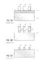
- FIGS. 1A-1D and 2illustrate an exemplary prior art method of forming multiple IC arrays.
- a target layer 120is provided over a substrate 110 .
- the target layer 120may be a hard mask layer, a spacer layer, or part of a substrate (e.g., a metal layer or interlevel dielectric).
- a resist layer 130is then provided over the target layer 120 .
- the resist layer 130is patterned to provide a mask for a plurality of arrays 101 a and 101 b , as shown in FIG. 1B .
- the resist layer 130is patterned to expose peripheral regions.
- the target layer 120is etched through the patterned resist layer 130 .
- FIG. 1Dillustrates a top plan view of four exemplary arrays 101 a - 101 d. It will be understood that the size, pattern and number of features in the arrays are simplified for purposes of illustration.
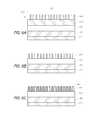
- FIGS. 4A-4H and 5 A- 5 Cillustrate a method for patterning IC device arrays according to an embodiment.
- a target layer 420is provided over a substrate 410 .
- the target layer 420may be a hard mask layer, a spacer layer, or part of the substrate 410 (e.g., a metal layer, a semiconductor layer, or an interlevel dielectric layer).
- a resist layer 430is provided over the target layer 420 .
- the resist layer 430is patterned to provide a mask for forming a repeating pattern 411 of features in the target layer 420 .
- the target layer 420is processed using the patterned resist layer 430 as a mask, as shown in FIG. 4C .
- processingcomprises etching to transfer the pattern from the resist layer 430 to the target layer 420 .
- FIG. 4Dthe resist layer 430 is removed, leaving only the target layer 420 having the repeating pattern of features.
- FIG. 5Aillustrates a top plan view of the target layer 420 having a line and space pattern.
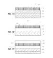
- the array regions 402are where IC devices employing the repeating pattern (e.g., memory arrays) are to be formed, whereas different patterns of features (e.g., for memory logic circuitry) are typically formed in the peripheral regions 403 .
- the array regions 402are preferably in a matrix form. In the illustrated embodiment, the array regions 402 have the same pattern as each other.
- the peripheral regions 403refer to regions lying between the array regions 402 and surrounding the array regions 402 . In the illustrated embodiment, at this stage, the peripheral regions 403 have a repeating pattern substantially identical to that of adjoining array regions. As shown in FIG. 4D , a peripheral region 403 has the same or similar line and space pattern as an adjoining array region 402 .
- features in the array regionsare referred to as “live features” whereas those having the same pattern in the peripheral regions are referred to as “dummy” features in the context of this document.
- the features (dummy features) of the patterned target layer 420 in the peripheral regions 403are etched using any conventional etch process, such as a dry etch process.
- the masking portions 440 a and 440 bare removed from the array regions 402 . Only the array regions 402 have a pattern of features for IC elements, for example, line-and-space patterns in the illustrated embodiment.
- FIG. 5Cillustrates a top plan view of resulting arrays 421 on the substrate 410 .
- each of the array regions 421can be further processed to complete the memory arrays.
- the featurescan represent trenches, conductive lines, portions of capacitors, portions of transistors, contacts, etc.
- a repeating pattern of featuresis formed throughout a first region of a substrate before using a non-critical mask to differentiate array and peripheral regions within the first region.
- edge non-uniformityis pushed to outermost edges of the first region, where the features are subsequently removed.
- features in the array regionsare subject to less local loading effects. Therefore, the center-to-edge non-uniformity can be reduced.
- the non-critical additional blocking mask step described abovemay be performed on spacers used for a pitch doubling process.
- pitch doublingor “pitch multiplication” is one proposed method for extending the capabilities of photolithographic techniques beyond their minimum pitch.
- a pitch multiplication methodis described in U.S. Pat. No. 5,328,810, issued to Lowrey et al., the entire disclosure of which is incorporated herein by reference.
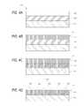
- FIGS. 3A-3Fillustrate a prior art pitch-doubling process for integrated circuit devices.
- a pattern of lines 310is photolithographically formed in a photoresist layer, which overlies a layer 320 of an expendable material, which in turn overlies a substrate 330 .
- the patternis then transferred using an etch (preferably an anisotropic etch) to the layer 320 , thereby forming placeholders, or mandrels, 340 .
- the photoresist lines 310can be stripped and the mandrels 340 can be isotropically etched to increase the distance between neighboring mandrels 340 , as shown in FIG. 3C .
- the same widthnow includes two features and two spaces, with the spaces defined by, e.g., the spacers 360 .
- the smallest feature size possible with a photolithographic techniqueis effectively decreased.
- the first hard mask layer 630may be formed of an inorganic material.
- the first hard mask layer 630is formed of polysilicon, low silane oxide (LSO), silicon oxide, silicon nitride (Si 3 N 4 ) or silicon oxynitride (SiO x N y ).
- the first hard mask layer 630may have a two-layered structure, including a silicon upper layer and an LSO lower layer or an inorganic hard mask (e.g., 600 ⁇ of silicon or LSO) over a supplemental hard mask layer such as transparent carbon (t-C).
- the second hard mask layer 640may be formed of amorphous carbon and may serve as a sacrificial or mandrel layer for forming spacers.
- a preferred type of amorphous carbonis a colorless, transparent carbon that facilitates photo alignment to underlying layers.
- the second hard mask layer 640may have a thickness of between about 600 ⁇ and about 2,000 ⁇ , more preferably between about 1,000 ⁇ and about 1,400 ⁇ . Details of a pitch doubling process employing multiple hard mask layers beneath the mandrel layer are described in U.S. patent application Ser. No. 11/214,544 to Tran et al., filed Aug. 29, 2005, the entire disclosure of which is incorporated herein by reference. Thus, while illustrated with two hard mask layers, the processes described herein can employ a greater number or fewer hard mask layers.
- a resist layer 650is provided over the second hard mask layer 640 .
- a material for the resist layer 650is selected based on the type of lithography used for patterning the resist layer 650 .
- Examples of such lithographyinclude, but are not limited to, ultraviolet (UV) lithography, extreme ultraviolet (EUV) lithography, X-ray lithography and imprint contact lithography.
- the UV lithographyincludes 157 nm photolithography, 193 nm photolithography, and 248 nm photolithography.
- the 248 nm photolithographyis also referred to as “Deep Ultraviolet (DUV)” lithography.
- DUV photolithographyis used for patterning the resist layer 650 .
- the resist layer 650is formed of a DUV resist which is commercially available. A skilled artisan will appreciate that the material of the layers may be varied depending on lithography, availability of selective etch chemistries and IC design.
- a bottom anti-reflective coating (BARC) layermay be provided between the resist layer 650 and the second hard mask layer 640 .
- BARCswhich are typically organic, enhance the resolution by preventing reflections of the ultraviolet (UV) radiation that activates the photoresist.
- UV radiationultraviolet
- BARCsare widely available, and are usually selected based upon the selection of the resist material and the UV wavelength.
- BARCswhich are typically polymer-based, are usually removed along with the overlying photoresist.
- the optional BARC layerpreferably has a thickness of between about 200 ⁇ and about 600 ⁇ , more preferably between about 300 ⁇ and about 500 ⁇ .
- the resist layer 650has been patterned using a DUV photolithographic process.
- the resist layer 650may be patterned using any suitable resist patterning technique.
- the illustrated resist layer 650has a repeating pattern of features throughout a first region 601 which includes array regions and peripheral regions. The peripheral region will ultimately have no features from this pattern in the target layer 620 .
- the resist 650has been patterned to provide substantially the same features in the peripheral regions as in the array regions.
- the patternonly includes a straight line-and-space pattern. In other embodiments, the pattern may include various other shapes.
- the second hard mask layer 640is etched using the patterned resist 650 as a mask.
- the repeating pattern of features in the resist 650is transferred into the second hard mask layer 640 .
- the second hard mask 640is preferably etched using a plasma etch process, most preferably a high-density plasma etch process.
- a pattern transfer from the resist layer 650 into the second hard mask layer 640is preferably accomplished using an oxygen-containing plasma dry etch in Lam Research Corp.'s (Fremont, Calif.) TCP9400 poly etch chamber or Applied Material Corp.'s (Santa Clara, Calif.) IPS oxide etch chamber.
- Preferred precursor gasesinclude HBr/O 2 /N 2 and SO 2 /O 2 .
- the resist layer 650is then removed, as shown in FIG. 6B .
- features in the resist layer 650 ( FIG. 6A ) or features in the second hard mask layer 640 ( FIG. 6B )are trimmed or shrunk to increase the distance between neighboring features, as discussed with respect to FIG. 3C .
- a layer 660 of spacer materialis blanket-deposited conformally over exposed surfaces, including the first hard mask layer 630 and the top and sidewalls of the second hard mask layer 640 .
- the spacer materialis preferably deposited by chemical vapor deposition or atomic layer deposition.
- the spacer materialcan be any material capable of use as a mask to transfer a pattern to the underlying first hard mask layer 630 .
- the spacer materialpreferably: 1) can be deposited with good step coverage, 2) can be deposited at a low temperature compatible with the second hard mask layer 640 and 3) can be selectively etched relative to the second hard mask layer 640 and preferably also relative to the material directly underlying the second hard mask layer 640 .
- the spacer material 660is silicon oxide and the underlying first hard mask layer 630 is selectively etchable, such as silicon, silicon nitride, silicon oxynitride (e.g., DARC) or silicon over LSO, which provides particular advantages in combination with other selected materials of the masking stack.
- the spacer materialmay be polysilicon or low temperature oxide (LTO).
- the spacer depositionis performed directly on the patterned resist layer 650 ( FIG. 6A ). In such embodiments, the second hard mask layer 640 may be omitted.
- the spacer layer 660is then subjected to an anisotropic etch to remove spacer material from horizontal surfaces 661 of the partially formed integrated circuit 600 .
- an etchalso known as a spacer etch
- a fluorocarbon plasmae.g., containing CF 4 /CHF 3 , C 4 F 8 /CH 2 F 2 or CHF 3 /Ar plasma.
- These exemplary etchantsare selective for silicon oxide relative to carbon of the second hard mask layer 640 and polysilicon or silicon over LSO of the first hard mask layer 630 .
- the pitch of the spacers 662is roughly half that of the photoresist lines and spaces ( FIG. 6A ) originally formed by photolithography. Where the photoresist lines had a pitch of about 200 nm, spacers 662 having a pitch of about 100 nm or less can be formed. It will be appreciated that because the spacers 662 are formed on the sidewalls of the features or lines, the spacers 662 generally follow the outline of the pattern of features or lines in the patterned resist 650 and, so, typically form a closed loop in the spaces between the lines. The spacers 662 form a repeating pattern 611 of features in the first region 601 of the substrate.
- an additional blocking mask 670is provided over exposed surfaces, including the first hard mask layer 630 and the top and sidewalls of the spacers 662 as shown in FIG. 6F .
- the additional mask 670is preferably a soft mask and may have the same thickness and material as the blocking mask layer 440 described above with reference to FIG. 4E .
- the additional mask 670is patterned to cover or block array regions 602 while opening peripheral regions 603 as shown in FIG. 6G .
- spacers in the peripheral regions 603are etched using the patterned mask 670 , preferably selectively relative to the underlying first hard mask. During this step, the spacers in the peripheral regions 603 are etched away as shown in FIG. 6H .
- the blocking mask 670 overlying the first hard mask layer 630 and the spacers 662is then removed.
- the mask 670is removed using any conventional process selective for the mask 670 relative to the first hard mask layer 630 and the spacers 662 .
- a pattern provided by the spacers 662is transferred into the first hard mask layer 630 as shown in FIG. 6J .
- the pattern transfercan be performed using any suitable etch process selective for the first hard mask layer 630 relative to the spacers 662 .
- a preferred etchant for the first hard mask layer 630is HBr/Cl 2 .
- the etch processis preferably a dry, anisotropic plasma etch process. In the illustrated embodiment, an anisotropic plasma etch process is used to minimize undesired lateral etching of the first hard mask layer 630 .
- a pattern in first hard mask layer 630is transferred into the target layer 620 to form arrays.
- the pattern transferis performed by etching the target layer 620 using the patterned first hard mask layer 630 as a mask.
- the etch processis preferably a dry, anisotropic etch process.
- the blocking mask 670may also serve to remove or cut spacer loop ends.
- spacersare formed on sidewalls of features or lines, for examples, the features of the second hard mask layer 640 in FIG. 6C .
- the spacersthus generally follow the outline of the pattern of features or lines over which the spacers are deposited and, so, typically form a closed loop, either within trenches in the spaces between the lines, or around isolated line features. Consequently, where the pitch multiplied pattern is used to form conductive lines, additional processing steps are preferably used to cut off the ends of these loops, so that each loop forms two individual, non-connected lines.
- the additional blocking mask 670 of the embodiment described abovecan serve as a protective mask for the parts of the lines to be maintained. Details about other methods for cutting off the ends of the loops are disclosed in U.S. patent application Ser. No. 10/931,771 to Tran et al., filed Aug. 31, 2004, the entire disclosure of which is incorporated be reference herein.
- the additional mask step described abovemay be performed for a pitch doubling process in conjunction with a process for forming a damascene structure.
- a “damascene” structurerefers to a structure having metal structures inlaid within recesses formed in a layer of dielectric. The metal may constitute an interconnect line. The inlaid metal of the damascene structure is typically isolated within trenches by means of a chemical-mechanical planarization or polishing (CMP) process.
- CMPchemical-mechanical planarization or polishing
- trenchesare first defined lithographically in a dielectric layer. Then, a metal is deposited to fill the trenches. Subsequently, excess metal is removed by CMP.
- a resist layer 750is provided and patterned over the second hard mask layer 740 .
- the resist 750has a repeating pattern of features throughout a first region 701 , which includes array regions 702 and peripheral regions 703 .
- the peripheral regions 703will ultimately have no features in the target layer 720 .
- the resist 750has been patterned to provide substantially the same features in the peripheral regions 703 as in the array regions 702 .
- the second hard mask layer 740is etched using the patterned resist 750 as a mask.
- the repeating pattern of features in the resist 750is transferred into the second hard mask layer 740 .
- trimming or shrinkingis performed either at the resist 750 stage ( FIG. 7A ) or at the second hard mask 740 stage ( FIG. 7B ) to increase the distance between neighboring features, as discussed with respect to FIG. 3C .
- Preferred methods for spacer material depositioninclude chemical vapor deposition, e.g., using O 3 and TEOS to form silicon oxide, and atomic layer deposition, e.g., using a silicon precursor with an oxygen or nitrogen precursor to form silicon oxides and nitrides, respectively.
- the thickness of the layer 760is preferably determined based upon the desired width of the spacers 762 ( FIG. 7F ).
- the layer 760is preferably deposited to a thickness of about 20-80 nm and, more preferably, about 40-60 nm.
- the step coverageis about 80% or greater and, more preferably, about 90% or greater.
- the spacer layer 760is then subjected to an anisotropic etch to remove spacer material from horizontal surfaces 761 of the partially formed integrated circuit 700 .
- an etchalso known as a spacer etch, can be selectively performed for the preferred silicon oxide material 760 using a fluorocarbon plasma, e.g., containing CF 4 /CHF 3 , C 4 F 8 /CH 2 F 2 or CHF 3 /Ar plasma.
- the mandrels formed by the second hard mask layer 740are next removed to leave freestanding spacers 762 .
- the second hard mask layer 740is selectively removed.
- Preferred etch chemistries for the preferred carbon mandrelsinclude an oxygen-containing plasma etch, such as an etch using HBr/O 2 /N 2 and SO 2 /O 2 .
- the resulting spacers 762form a repeating pattern 711 of features in the first region 701 of the substrate.
- an additional blocking mask 770is provided over exposed surfaces, including the first hard mask layer 730 and the top and sidewalls of the spacers 762 as shown in FIG. 7F .
- the additional mask 770may have the same thickness and material as the mask 670 described above with reference to FIG. 6F .
- the additional mask 770(a non-critical mask with large dimensions) is patterned to open array regions 702 , as shown in FIG. 7G , while covering peripheral regions 703 .
- the top and sidewalls of the spacers 762 and parts of the upper surface of the first hard mask layer 730 in the array regions 702are exposed.
- the blocking mask 770 overlying the spacers 762 in the peripheral regions 703is removed using any suitable process.
- the spacers 762are removed using an etch process, as shown in FIG. 7I , leaving behind the patterned first hard mask layer 730 .
- the first hard mask layer 730now has a line and space pattern in the array regions 702 , but not in the peripheral regions 703 .
- two hard mask layers 730 , 740are employed for a pattern transfer from the resist 750 into the target layer 720 .
- only one hard mask layer or more than two hard mask layersmay be used for a pattern transfer between a resist and a target layer.
- a pattern in the spacer layer 760( FIG. 7G ) is transferred into the substrate or target layer 720 without removing the spacer layer 760 and the blocking mask 770 as shown in FIG. 7I .
- the pattern in the spacer layer 760can be transferred into the target layer 720 by a single etch step or consecutive etch steps, whether or not the intervening first hard mask layer 730 is used.
- the blocking mask 770can also be used for blocking spacer loop ends of the live (array) features, such that these portions of the patterns are not etched into the dielectric target layer 720 .
- FIGS. 8A-8Ia method of patterning and etching for IC device arrays using a hard mask according to another embodiment is described.
- the hard maskis provided with a repeating pattern of features.
- an additional (non-critical) blocking maskis provided over the patterned hard mask to define array regions and peripheral regions.
- This embodimentis similar to the embodiment of FIG. 4 with extra hard mask layers and intervening transfer steps.
- a target layer 820is provided over a substrate 810 .
- the target layer 820may be considered part of the substrate 810 and may represent, e.g., a blanket metal layer to be patterned.
- a hard mask layer 830is provided over the target layer 820 .
- a resist layer 840is provided over the hard mask layer 830 .
- the substrate 810 , the target layer 820 , and the resist layer 840may have the same thicknesses and materials as those described above with reference to FIGS. 6 and 7 .
- the hard mask layer 830will be used to transfer a pattern from the resist layer 840 into the target layer 820 .
- the hard mask layer 830may be formed of an organic material, preferably amorphous carbon.
- a preferred type of amorphous carbonis a colorless, transparent carbon that facilitates photo alignment to underlying layers.
- the hard mask layer 830may have a thickness of between about 1,000 ⁇ and about 4,000 ⁇ , more preferably between about 2,000 ⁇ and about 3,000 ⁇ .
- the hard mask layer 830may have an upper hard mask and a lower hard mask.
- the upper hard maskmay be formed of amorphous carbon.
- the lower hard maskmay be formed of polysilicon, silane oxide, silicon oxide, or silicon nitride.
- the lower hard maskmay have a two-layered structure, including a silicon top layer and a silane oxide bottom layer.
- a bottom anti-reflective coating (BARC) layermay optionally be provided between the hard mask layer 830 and the resist 840 .
- BARCsare widely available, and are usually selected based upon the selection of the resist material and the UV wavelength.
- the BARC layermay have a thickness of between about 200 ⁇ and about 1,000 ⁇ , more preferably between about 300 ⁇ and about 600 ⁇ .
- An additional hard mask layer(not shown) may also be provided over the hard mask layer to provide excellent pattern transfer fidelity.
- the additional hard mask layermay be formed of a DARC.
- the resist layer 840is patterned to provide a repeating pattern 811 of features in a first region 801 of the substrate 810 .
- the first region 801includes a plurality of array regions 802 and peripheral regions 803 outside the array regions 802 within the first region 801 .
- the repeating patternis provided throughout the first region 801 without distinction of the array and peripheral regions 802 , 803 which will be later defined.
- the array regionsare where IC devices are to be formed and will include identical IC elements.
- the peripheral regionsinclude gaps or spaces which surround the array regions and in which typically logic circuitry is formed.
- the pattern 811 in the peripheral regionis substantially similar to that of an adjacent array region.
- the pattern in the resist layer 840is transferred into the hard mask layer 830 .
- the pattern transferis preferably performed by using a plasma etch process, most preferably a high-density plasma etch process.
- the plasma etch processis an anisotropic etch process. This etch process may have the same chemistry and conditions as the method described for etching the hard mask layer in embodiments discussed above.
- an additional blocking mask 850is provided over the patterned hard mask layer 830 .
- the mask 850covers exposed surfaces, including the target layer 820 and the top and sidewalls of the hard mask layer 830 . Then, the mask 850 is patterned to cover array regions 802 and to open the peripheral regions 803 , as shown in FIG. 8F .
- FIG. 8Gthe hard mask layer 830 in the peripheral regions 803 is etched through openings of the patterned mask layer 850 .
- exposed features in the peripheral regions 803are etched away, as shown in FIG. 8G .
- the mask layer 850 overlying the hard mask layer 830is removed by any conventional method, as shown in FIG. 8H .
- a pattern in the hard mask layer 830is transferred into the target layer 820 , as shown in FIG. 81 .
- the pattern transfercan be performed using any suitable etch process selective for the target layer 820 relative to the hard mask layer 830 .
- the etch processmay be a dry etch process or a wet etch process.
- an anisotropic plasma etch processis used for a faithful pattern transfer into the target layer 820 .
- the hard mask layer 830is removed by an etch process selective for the hard mask 830 relative to the target layer 820 and exposed underlying substrate 810 , leaving behind arrays in the array regions 802 .
- the substratewill be further provided with additional layers or materials to complete IC devices.
- FIGS. 9A-9Hillustrate a method of forming a damascene structure using an additional blocking mask on a hard mask according to another embodiment.
- a hard mask layeris provided with a repeating pattern of features in a first region.
- an additional blocking maskis provided over the patterned hard mask to define array regions and peripheral regions in the first region.
- a target layer 920is provided over a substrate 910 .
- the target layeris formed of a dielectric material, typically a form of silicon oxide.
- a hard mask layer 930is provided over the target layer 920 .
- a resist layer 940is provided over the hard mask layer 930 .
- the layers 910 - 940may have similar thicknesses and materials as those described above with reference to FIGS. 8A-8J .
- the resist layer 940is patterned to provide a repeating pattern 911 of features to the hard mask layer 930 .
- the pattern 911includes substantially the same features throughout the first regions 901 in both array regions 902 and peripheral regions 903 ( FIG. 9D ) which will be later defined.
- the hard mask layer 930is etched through openings of the resist layer 940 , as shown in FIG. 9C .
- Any suitable etchantcan be used to selectively etch the hard mask layer 930 relative to the resist layer 940 .
- an anisotropic dry etch processis used. More preferably, a high-intensity plasma etch process is used for etching the hard mask layer 930 .
- An additional hard mask layer(not shown) may be provided over the hard mask layer to provide excellent pattern transfer fidelity.
- the additional hard mask layermay be formed of a DARC.
- a BARC layer(not shown) may be provided between the additional hard mask layer and the resist layer.
- a blocking mask 950is provided over the patterned hard mask layer 930 .
- the blocking mask 950is preferably a soft mask formed of a resist, more preferably, a photoresist. A material for the resist is selected based on the lithographic process for patterning the resist.
- the blocking mask 950fills spaces 931 in the hard mask layer 930 resulting from the etching step described above. In addition to filling the spaces 931 , the blocking mask 950 covers top surfaces of the hard mask layer 930 .
- the blocking mask 950has a thickness of between about 2,000 ⁇ and about 11,000 ⁇ , more preferably between 5,000 ⁇ and about 7,000 ⁇ .
- the blocking non-critical mask 950is patterned to define the array regions 902 and peripheral regions 903 .
- the mask layer 950is patterned to expose the array regions 902 and cover the peripheral regions 903 .
- the blocking mask 950is patterned using a selected lithographic process. When patterning the blocking mask 940 , the resist which has filled the spaces 931 is also removed to expose parts of the target layer surface as shown in FIG. 9F .
- the target layer 920is etched through the hard mask layer 930 .
- trenches 921are formed in the array regions 902 .
- the hard mask layer 930 and the blocking mask 950are removed as shown in FIG. 9H .
- a metal or its alloyis provided into the trenches 921 .
- the metalmay be one typically used to form an interconnect metal line. Examples of the metal include, but are not limited to, copper, silver, and gold. Subsequently, excess metal is polished to provide a planar surface on the top, as shown in FIG. 91 .
- Another aspect of the inventionprovides an IC device having arrays made by the method described above.
- the methodmay be preferably used for fabricating IC device arrays having features which have a critical dimension of less than 100 nm, more preferably less than 60 nm and a line density of between about 5 lines/ ⁇ m (100 nm nodes) and about 20 lines/ ⁇ m (25 nm nodes).
- a resulting IC device arraypreferably has optimal center-to-edge uniformity.
- the center-to-edge uniformityis expressed in terms of center-to-edge deviation.
- the term “center-to-edge deviation,” as used herein,refers to a measure of a degree of disparity in feature widths provided that features of the same width are transferred from a resist into center and edge portions of an IC array. The deviation is denoted as percentage of a difference of an edge feature width relative to a center feature width.
- a center-to-edge deviation of 10%is obtained if features of the same width result in 100 nm-width in a center portion and 110 nm-width in an edge portion, or 100 nm-width in a center portion and 90 nm-width in an edge portion.
- the resulting IC device arrayhas a center-to-edge line width deviation of between about 0% and about 5%, more preferably between about 0% and about 1%.
- the electronic devicemay also include a system including a microprocessor and/or a memory device.
- a systemmay be a computer system, an electronic system, or an electromechanical system.
- the electronic devicemay include, but is not limited to consumer electronic products, electronic circuits, electronic circuit components, parts of the consumer electronic products, electronic test equipments, etc.
- the consumer electronic productsmay include, but are not limited to, a mobile phone, a telephone, a television, a computer monitor, a computer, a hand-held computer, a personal digital assistant (PDA), a microwave, a refrigerator, a stereo system, a cassette recorder or player, a DVD player, a CD player, a VCR, an MP3 player, a radio, a camcorder, a camera, a digital camera, a portable memory chip, a washer, a dryer, a washer/dryer, a copier, a facsimile machine, a scanner, a multi functional peripheral device, a wrist watch, a clock, etc.
- the electronic devicemay include unfinished intermediate products.
- a pattern of featuresis formed across multiple arrays and intervening peripheries (and outer borders). Then, a pattern is removed from the peripheries (conventional patterning) or blocked from transfer to substrate (damascene) using a non-critical blocking mask which is inexpensive and easy to pattern.
- the blocking maskcan also double in function to chop spacer loop ends (conventional patterning) or prevent spacer loop ends from transferring into substrate (damascene). The embodiments have advantage of pushing non-uniformities of arrays out to peripheral regions where they will be rendered nonoperative or removed by blocking mask.
- a methodfor patterning integrated circuit (IC) device arrays.
- the methodcomprises forming a repeating pattern of features in a masking layer across a first region of a substrate.
- a blocking maskis applied over the features in the masking layer.
- the blocking maskdifferentiates array regions of the first region from peripheral regions of the first region.
- the pattern of features in the array regionsis transferred into the substrate.
- a methodfor forming memory device arrays.
- the methodcomprises forming a repeating pattern of features in a first layer across a first region of a substrate.
- a second layeris applied over the features in the first layer.
- the second layeris configured to cover a plurality of array regions within the first region and to open non-array regions within the first region outside the array regions, thereby exposing features in the non-array regions.
- the exposed features in the non-array regions of the first layerare removed while the second layer covers the plurality of array regions.
- an intermediate integrated circuit structurecomprising a substrate comprising a plurality of array regions and peripheral regions surrounding and between the array regions.
- the structurealso includes a first layer formed over the substrate.
- the first layercomprises a repeating pattern of features across both the array and peripheral regions.
Landscapes
- Engineering & Computer Science (AREA)
- Microelectronics & Electronic Packaging (AREA)
- Condensed Matter Physics & Semiconductors (AREA)
- General Physics & Mathematics (AREA)
- Manufacturing & Machinery (AREA)
- Computer Hardware Design (AREA)
- Physics & Mathematics (AREA)
- Power Engineering (AREA)
- Chemical & Material Sciences (AREA)
- Inorganic Chemistry (AREA)
- Internal Circuitry In Semiconductor Integrated Circuit Devices (AREA)
- Semiconductor Memories (AREA)
- Drying Of Semiconductors (AREA)
- General Engineering & Computer Science (AREA)
Abstract
Description
- This application is a divisional of U.S. patent application Ser. No. 12/360,738, filed Jan. 27, 2009, which is a continuation of U.S. patent application Ser. No. 11/411,401, filed Apr. 25, 2006 (now U.S. Pat. No. 7,488,685), the disclosure of which is hereby incorporated by reference in its entirety herein.
- This application is related to and incorporates the following by reference in their entireties: U.S. patent application Ser. No. 10/931,772 to Abatchev et al., filed Aug. 31, 2004; U.S. patent application Ser. No. 10/934,778 to Abatchev et al., filed Sep. 2, 2004; and U.S. patent application Ser. No. 11/214,544 to Tran et al., filed Aug. 29, 2005.
- 1. Field of the Invention
- The present invention relates to the field of integrated circuit fabrication, particularly to a process for improving critical dimension uniformity for integrated circuit arrays.
- 2. Description of the Related Art
- In the semiconductor industries, integrated circuit (IC) devices have become faster, smaller, and more efficient. This trend has continued with the development of fabrication technology to increase circuit densities on chips.
- Reducing critical dimension is one important way to increase circuit densities. The critical dimension (CD) is the dimension of the smallest geometrical features (width of interconnect line, contacts, trenches, etc.) formed during semiconductor device manufacturing. Critical dimensions need to be reduced in order to facilitate the formation of smaller features and faster, more efficient circuits.
- In fabricating certain IC devices with small CD, however, pattern non-uniformity occurs due to loading effects. Some IC devices have a number of identical circuit elements arranged in multiple arrays. Such IC devices are typically formed by simultaneously forming multiple arrays on a single semiconductor substrate. In arrays formed by certain methods, the inventors have found a tendency for edge portions to have different dimensions than central portions.
- The inventors have found certain processes, particularly hard mask formation and etch processes for dense feature arrays, are particularly subject to center-to-edge non-uniformities in each array. One possible source of non-uniformity may be that etchants and deposition precursors are not uniformly diffused into edge portions and central portions of arrays during an etch process that forms the arrays. Such non-uniformity occurs more significantly with denser line and space patterns. In addition, the inventors have also found spacer formation in a pitch-doubling process to result in center-to-edge non-uniformity. During the process, deposited spacers tend to be thicker in edge portions than in central portions of arrays.
- Attempts have been made to prevent such non-uniformity using Optical Proximity Correction (OPC) techniques. OPC is a reticle correction technique to remedy line-end shortening, rounding, or distortion problems in photolithography. The problems are typically caused by light refraction and scattering by edges of a patterned light blocking material in a reticle. However, the attempts have not been successful in remedying the center-to-edge non-uniformity.
- These and other aspects of the invention will be better understood from the Detailed Description of the Preferred Embodiments and from the appended drawings, which are meant to illustrate and not to limit the invention, and wherein:
FIGS. 1A-1D are schematic cross-sections illustrating a prior art process of etching for integrated circuit device arrays;FIG. 2 is a schematic top plan view of integrated circuit device arrays resulting from the process ofFIGS. 1A-1D ;FIGS. 3A-3F are schematic cross-sections illustrating a prior art pitch-doubling process for integrated circuit devices.FIGS. 4A-4H are schematic cross-sections illustrating a process of etching for integrated circuit device arrays in accordance with an embodiment of the invention;FIGS. 5A ,5B, and5C are schematic top plan views of the integrated circuit device arrays ofFIGS. 4D ,4F, and4H, respectively;FIGS. 6A-6K are schematic cross-sections illustrating a process of etching for integrated circuit device arrays in accordance with another embodiment of the invention, in which spacers are defined across several array regions prior to removal from peripheral regions;FIGS. 7A-7J are schematic cross-sections illustrating a damascene process for integrated circuit device arrays in accordance with another embodiment of the invention, in which spacers are defined across several array regions and their transfer to a lower level is blocked in peripheral regions;FIGS. 8A-8J are schematic cross-sections illustrating a process of etching for integrated circuit device arrays in accordance with another embodiment of the invention, in which repeating patterns are formed across several array regions prior to removal from peripheral regions; andFIGS. 9A-9I are schematic cross-sections illustrating a damascene process for integrated circuit device arrays in accordance with another embodiment of the invention, in which repeating patterns are defined across several array regions but their transfers to a lower level is blocked in peripheral regions.- In the context of this document, the term “integrated circuit (IC) device” refers to a semiconductor device, including, but not limited to, a memory device and a microprocessor. The memory device may be volatile memories such as random access memories (RAMs) or non-volatile memories such as read-only memories (ROMs). Examples of RAMs include dynamic random access memories (DRAMs) and static random access memories (SRAMs). Examples of ROMs include programmable read-only memories (PROMs), erasable programmable read-only memories (EPROMs), electrically-erasable programmable read-only memories (EEPROMs), and flash memories.
- The term “semiconductor substrate” is defined to mean any construction comprising semiconductor materials, including, but not limited to, bulk semiconductor materials such as a semiconductor wafer (either alone or in integrated assemblies comprising other materials thereon) and semiconductor material layers (either alone or in integrated assemblies comprising other materials). The term “substrate” refers to any supporting substrate, including, but not limited to, the semiconductor substrates described above. Also in the context of this document, the term “layer” encompasses both the singular and the plural unless otherwise indicated.
- The term, “features,” as used herein, refers to parts of a pattern, such as lines or spaces.
- The term “array” refers to a regularly repeating pattern of IC elements on a semiconductor substrate. For example, a memory array typically has a number of identical memory cells in a matrix form. Logic arrays may similarly include repeating patterns of conductive lines and/or transistors.
- The term, “target layer,” as used herein, refers to a layer in which arrays are formed. A target layer may be part of a semiconductor substrate. A target layer may include metal, semiconductor, and/or insulator.
- It will also be appreciated that transferring a pattern from a first (e.g., masking) level to a second level involves forming features in the second level that generally correspond to features on the first level. For example, the path of lines in the second level will generally follow the path of lines on the first level. The location of other features on the second level will correspond to the location of similar features on the first level. The precise shapes and sizes of corresponding features can vary from the first level to the second level, however due, for example, to trim and growth steps. As another example, depending upon etch chemistries and conditions, the sizes of and relative spacings between the features forming the transferred pattern can be enlarged or diminished relative to the pattern on the first level, while still resembling the same initial “pattern.”
- While “processing” through masks is described for preferred embodiments as etching to transfer a hard mask pattern into a target layer, the skilled artisan will appreciate that processing in other embodiments can comprise, e.g., oxidation, nitridation, selective deposition, doping, etc. through the masks.
FIGS. 1A-1D and2 illustrate an exemplary prior art method of forming multiple IC arrays. As shown inFIG. 1A , atarget layer 120 is provided over asubstrate 110. Thetarget layer 120 may be a hard mask layer, a spacer layer, or part of a substrate (e.g., a metal layer or interlevel dielectric). A resistlayer 130 is then provided over thetarget layer 120. Then, the resistlayer 130 is patterned to provide a mask for a plurality ofarrays FIG. 1B . In addition, the resistlayer 130 is patterned to expose peripheral regions. Next, as shown inFIG. 1C , thetarget layer 120 is etched through the patterned resistlayer 130. Then, as shown inFIG. 1D , the resistlayer 130 is removed, leavingarrays substrate 110.FIG. 2 illustrates a top plan view of four exemplary arrays101a-101d.It will be understood that the size, pattern and number of features in the arrays are simplified for purposes of illustration.- In the above prior art method, array and peripheral regions are defined at or prior to the stage at which a pattern in the resist
layer 130 is transferred into thetarget layer 120. Thus, the features are defined only in the array regions. According to an embodiment of the invention, however, a repeating pattern of features is first formed throughout a first region of a substrate. Then, array and peripheral regions are defined within the first region at an additional masking step. FIGS. 4A-4H and5A-5C illustrate a method for patterning IC device arrays according to an embodiment. As shown inFIG. 4A , atarget layer 420 is provided over asubstrate 410. Thetarget layer 420 may be a hard mask layer, a spacer layer, or part of the substrate410 (e.g., a metal layer, a semiconductor layer, or an interlevel dielectric layer). A resistlayer 430 is provided over thetarget layer 420. Next, as shown inFIG. 4B , the resistlayer 430 is patterned to provide a mask for forming arepeating pattern 411 of features in thetarget layer 420.- Subsequently, the
target layer 420 is processed using the patterned resistlayer 430 as a mask, as shown inFIG. 4C . In the illustrated embodiment, processing comprises etching to transfer the pattern from the resistlayer 430 to thetarget layer 420. Then, as shown inFIG. 4D , the resistlayer 430 is removed, leaving only thetarget layer 420 having the repeating pattern of features.FIG. 5A illustrates a top plan view of thetarget layer 420 having a line and space pattern. - In
FIGS. 4D and 5A , the repeatingpattern 411 of features has been formed in thetarget layer 420 in afirst region 401 of thesubstrate 410. Thefirst region 401 may occupy a certain area of a substrate surface. Thefirst region 401 includes a plurality ofarray regions 402 andperipheral regions 403. In the context of this document, array regions may also be referred to as active regions. Peripheral regions may also be referred to as inactive regions or non-array regions. The designation of “inactive” is merely a label relating to the pattern of repeating features; the skilled artisan will appreciate that active devices such as in logic circuitry are typically formed in the peripheral regions. Thearray regions 402 are where IC devices employing the repeating pattern (e.g., memory arrays) are to be formed, whereas different patterns of features (e.g., for memory logic circuitry) are typically formed in theperipheral regions 403. Thearray regions 402 are preferably in a matrix form. In the illustrated embodiment, thearray regions 402 have the same pattern as each other. Theperipheral regions 403 refer to regions lying between thearray regions 402 and surrounding thearray regions 402. In the illustrated embodiment, at this stage, theperipheral regions 403 have a repeating pattern substantially identical to that of adjoining array regions. As shown inFIG. 4D , aperipheral region 403 has the same or similar line and space pattern as an adjoiningarray region 402. Features in the array regions are referred to as “live features” whereas those having the same pattern in the peripheral regions are referred to as “dummy” features in the context of this document. - Next, as shown in
FIG. 4E , an additionalblocking mask layer 440 is provided over the patternedtarget layer 420.FIG. 4F illustrates the blockingmask layer 440 patterned to mask thearray regions 402. Thearray regions 402 are covered by maskingportions mask layer 440 whereas theperipheral regions 403 are exposed.FIG. 5B illustrates a top plan view of thefirst region 401 with the array regions covered by the maskingportions 440a-440d. As shown inFIG. 5B , theperipheral regions 403 are exposed. In another embodiment, the blocking mask layer is configured to mask peripheral regions and expose array regions. In such an embodiment, features in the array regions are etched to form trenches while the peripheral regions remain unprocessed. This embodiment is generally applicable to a damascene process as will be described in detail with reference toFIGS. 7 and 9 . - As shown in
FIG. 4G , the features (dummy features) of the patternedtarget layer 420 in theperipheral regions 403 are etched using any conventional etch process, such as a dry etch process. Subsequently, as shown inFIG. 4H , the maskingportions array regions 402. Only thearray regions 402 have a pattern of features for IC elements, for example, line-and-space patterns in the illustrated embodiment.FIG. 5C illustrates a top plan view of resultingarrays 421 on thesubstrate 410. - Although unpictured, after forming arrays as described above, the substrate will be further provided with additional layers or materials to complete IC devices. For example, each of the
array regions 421 can be further processed to complete the memory arrays. The features can represent trenches, conductive lines, portions of capacitors, portions of transistors, contacts, etc. - In the method described above, a repeating pattern of features is formed throughout a first region of a substrate before using a non-critical mask to differentiate array and peripheral regions within the first region. Thus, edge non-uniformity is pushed to outermost edges of the first region, where the features are subsequently removed. Thus, features in the array regions are subject to less local loading effects. Therefore, the center-to-edge non-uniformity can be reduced.
- The non-critical additional blocking mask step described above may be performed on spacers used for a pitch doubling process. “Pitch doubling” or “pitch multiplication” is one proposed method for extending the capabilities of photolithographic techniques beyond their minimum pitch. A pitch multiplication method is described in U.S. Pat. No. 5,328,810, issued to Lowrey et al., the entire disclosure of which is incorporated herein by reference.
FIGS. 3A-3F illustrate a prior art pitch-doubling process for integrated circuit devices. With reference toFIG. 3A , a pattern oflines 310 is photolithographically formed in a photoresist layer, which overlies alayer 320 of an expendable material, which in turn overlies asubstrate 330. As shown inFIG. 3B , the pattern is then transferred using an etch (preferably an anisotropic etch) to thelayer 320, thereby forming placeholders, or mandrels,340. The photoresist lines310 can be stripped and themandrels 340 can be isotropically etched to increase the distance between neighboringmandrels 340, as shown inFIG. 3C . Alayer 350 of spacer material is subsequently blanket deposited over themandrels 340, as shown inFIG. 3D .Spacers 360, i.e., the material extending or originally formed extending from sidewalls of another material, are then formed on the sides of themandrels 340. The spacer formation is accomplished by preferentially etching the spacer material from thehorizontal surfaces FIG. 3E . The remainingmandrels 340 are then removed, leaving behind only thespacers 360, which together act as a mask for patterning, as shown inFIG. 3F . Thus, where a given pitch previously included a pattern defining one feature and one space, the same width now includes two features and two spaces, with the spaces defined by, e.g., thespacers 360. As a result, the smallest feature size possible with a photolithographic technique is effectively decreased.- While the pitch is actually halved in the example above, this reduction in pitch is conventionally referred to as pitch “doubling,” or, more generally, pitch “multiplication.” Thus, conventionally, “multiplication” of pitch by a certain factor actually involves reducing the pitch by that factor. That is because pitch is used with two converse meanings: the distance between identical features in a repeating pattern (which decreases with increasing density) and the number of features per linear distance (which increases with increasing density).
- As explained above, where a given pitch previously included a pattern defining one feature and one space, the same width now includes two features and two spaces. In other words, a pitch-doubled pattern is twice as dense as a conventional pattern. Similarly, when pitching doubling is applied to forming IC device arrays, resulting arrays have a pattern twice as dense as conventional arrays. Accordingly, the center-to-edge non-uniformity caused by loading effects is more serious in pitch-doubled arrays than in conventional arrays.
- In view of the problem, preferred embodiments of the invention allow for improved center-to-edge uniformity in pitch-multiplied IC arrays. In a first phase of the method, photolithography and pitch multiplication are preferably used for forming a spacer pattern. The spacer pattern includes a repeating pattern of features in a first region of a substrate. The same repeating pattern is formed throughout the first region. Then, an additional non-critical mask step is performed to define a plurality of array regions and peripheral regions within the first region.
- With reference to
FIGS. 6A-6K , a method of patterning integrated circuit device arrays using pitch multiplication is described. As shown inFIG. 6A , atarget layer 620 is provided over asubstrate 610. Thetarget layer 620 may be considered part of thesubstrate 610. A firsthard mask layer 630 is provided over thetarget layer 620. A secondhard mask layer 640 is provided over the firsthard mask layer 630. The first hard mask is used as a mask for etching thetarget layer 620. In certain embodiments, the secondhard mask layer 640 may be omitted. - The first
hard mask layer 630 may be formed of an inorganic material. In one embodiment, the firsthard mask layer 630 is formed of polysilicon, low silane oxide (LSO), silicon oxide, silicon nitride (Si3N4) or silicon oxynitride (SiOxNy). In certain embodiments, the firsthard mask layer 630 may have a two-layered structure, including a silicon upper layer and an LSO lower layer or an inorganic hard mask (e.g., 600 Å of silicon or LSO) over a supplemental hard mask layer such as transparent carbon (t-C). It should be noted that the material for the firsthard mask layer 630 is chosen based on etch selectivity relative to the overlying second hard mask layer material and a spacer material which will be later described. For example, the material for the firsthard mask layer 630 is preferably selectively etchable relative to the spacer material. Additionally, the (upper layer of)underlying substrate 610 is preferably selectively etchable relative to the firsthard mask layer 630 such that they are of different materials. Preferably, the firsthard mask layer 630 may have a thickness of between about 200 Å and about 3,600 Å, more preferably between about 600 Å and about 2,600 Å. - The second
hard mask layer 640 may be formed of amorphous carbon and may serve as a sacrificial or mandrel layer for forming spacers. A preferred type of amorphous carbon is a colorless, transparent carbon that facilitates photo alignment to underlying layers. Preferably, the secondhard mask layer 640 may have a thickness of between about 600 Å and about 2,000 Å, more preferably between about 1,000 Å and about 1,400 Å. Details of a pitch doubling process employing multiple hard mask layers beneath the mandrel layer are described in U.S. patent application Ser. No. 11/214,544 to Tran et al., filed Aug. 29, 2005, the entire disclosure of which is incorporated herein by reference. Thus, while illustrated with two hard mask layers, the processes described herein can employ a greater number or fewer hard mask layers. - In addition, a resist
layer 650 is provided over the secondhard mask layer 640. A material for the resistlayer 650 is selected based on the type of lithography used for patterning the resistlayer 650. Examples of such lithography include, but are not limited to, ultraviolet (UV) lithography, extreme ultraviolet (EUV) lithography, X-ray lithography and imprint contact lithography. The UV lithography includes 157 nm photolithography, 193 nm photolithography, and 248 nm photolithography. The 248 nm photolithography is also referred to as “Deep Ultraviolet (DUV)” lithography. In the illustrated embodiment, DUV photolithography is used for patterning the resistlayer 650. The resistlayer 650 is formed of a DUV resist which is commercially available. A skilled artisan will appreciate that the material of the layers may be varied depending on lithography, availability of selective etch chemistries and IC design. - Optionally, a bottom anti-reflective coating (BARC) layer (not shown) may be provided between the resist
layer 650 and the secondhard mask layer 640. BARCs, which are typically organic, enhance the resolution by preventing reflections of the ultraviolet (UV) radiation that activates the photoresist. BARCs are widely available, and are usually selected based upon the selection of the resist material and the UV wavelength. BARCs, which are typically polymer-based, are usually removed along with the overlying photoresist. - The optional BARC layer preferably has a thickness of between about 200 Å and about 600 Å, more preferably between about 300 Å and about 500 Å.
- In
FIG. 6A , the resistlayer 650 has been patterned using a DUV photolithographic process. In other embodiments, the resistlayer 650 may be patterned using any suitable resist patterning technique. The illustrated resistlayer 650 has a repeating pattern of features throughout afirst region 601 which includes array regions and peripheral regions. The peripheral region will ultimately have no features from this pattern in thetarget layer 620. However, the resist650 has been patterned to provide substantially the same features in the peripheral regions as in the array regions. In the illustrated embodiment, the pattern only includes a straight line-and-space pattern. In other embodiments, the pattern may include various other shapes. - Subsequently, as shown in
FIG. 6B , the secondhard mask layer 640 is etched using the patterned resist650 as a mask. The repeating pattern of features in the resist650 is transferred into the secondhard mask layer 640. The secondhard mask 640 is preferably etched using a plasma etch process, most preferably a high-density plasma etch process. A pattern transfer from the resistlayer 650 into the secondhard mask layer 640 is preferably accomplished using an oxygen-containing plasma dry etch in Lam Research Corp.'s (Fremont, Calif.) TCP9400 poly etch chamber or Applied Material Corp.'s (Santa Clara, Calif.) IPS oxide etch chamber. Preferred precursor gases include HBr/O2/N2and SO2/O2. The resistlayer 650 is then removed, as shown inFIG. 6B . Preferably, either features in the resist layer650 (FIG. 6A ) or features in the second hard mask layer640 (FIG. 6B ) are trimmed or shrunk to increase the distance between neighboring features, as discussed with respect toFIG. 3C . - Next, as shown in
FIG. 6C , alayer 660 of spacer material is blanket-deposited conformally over exposed surfaces, including the firsthard mask layer 630 and the top and sidewalls of the secondhard mask layer 640. The spacer material is preferably deposited by chemical vapor deposition or atomic layer deposition. The spacer material can be any material capable of use as a mask to transfer a pattern to the underlying firsthard mask layer 630. The spacer material preferably: 1) can be deposited with good step coverage, 2) can be deposited at a low temperature compatible with the secondhard mask layer 640 and 3) can be selectively etched relative to the secondhard mask layer 640 and preferably also relative to the material directly underlying the secondhard mask layer 640. In the illustrated embodiment, thespacer material 660 is silicon oxide and the underlying firsthard mask layer 630 is selectively etchable, such as silicon, silicon nitride, silicon oxynitride (e.g., DARC) or silicon over LSO, which provides particular advantages in combination with other selected materials of the masking stack. In other embodiments, the spacer material may be polysilicon or low temperature oxide (LTO). In certain embodiments, the spacer deposition is performed directly on the patterned resist layer650 (FIG. 6A ). In such embodiments, the secondhard mask layer 640 may be omitted. - Preferred methods for spacer material deposition include chemical vapor deposition, e.g., using O3and TEOS to form silicon oxide, and atomic layer deposition, e.g., using a silicon precursor with an oxygen or nitrogen precursor to form silicon oxides and nitrides, respectively. Atomic Layer Deposition (ALD) has the advantages of both low temperature deposition and high conformality. The thickness of the
layer 660 is preferably determined based upon the desired width of the spacers662 (FIG. 6G ). For example, in one exemplary embodiment, thelayer 660 is preferably deposited to a thickness of about 20-80 nm and, more preferably, about 40-60 nm. Preferably, the step coverage is about 80% or greater and, more preferably, about 90% or greater. - With reference to
FIG. 6D , thespacer layer 660 is then subjected to an anisotropic etch to remove spacer material fromhorizontal surfaces 661 of the partially formedintegrated circuit 600. Such an etch, also known as a spacer etch, can be performed selectively on the preferred silicon oxide material, using a fluorocarbon plasma, e.g., containing CF4/CHF3, C4F8/CH2F2or CHF3/Ar plasma. These exemplary etchants are selective for silicon oxide relative to carbon of the secondhard mask layer 640 and polysilicon or silicon over LSO of the firsthard mask layer 630. - With reference to
FIG. 6E , the mandrels formed in the secondhard mask layer 640 are next removed to leavefreestanding spacers 662. The secondhard mask layer 640 is selectively removed. Preferred etch chemistries that selectively remove carbon without substantially etching inorganic materials include an oxygen-containing plasma etch, such as an etch using HBr/O2/N2and SO2/O2. - Thus, pitch multiplication has been accomplished. In the illustrated embodiment, the pitch of the
spacers 662 is roughly half that of the photoresist lines and spaces (FIG. 6A ) originally formed by photolithography. Where the photoresist lines had a pitch of about 200 nm,spacers 662 having a pitch of about 100 nm or less can be formed. It will be appreciated that because thespacers 662 are formed on the sidewalls of the features or lines, thespacers 662 generally follow the outline of the pattern of features or lines in the patterned resist650 and, so, typically form a closed loop in the spaces between the lines. Thespacers 662 form arepeating pattern 611 of features in thefirst region 601 of the substrate. - Next, in a second phase of methods according to the preferred embodiments, an
additional blocking mask 670 is provided over exposed surfaces, including the firsthard mask layer 630 and the top and sidewalls of thespacers 662 as shown inFIG. 6F . Theadditional mask 670 is preferably a soft mask and may have the same thickness and material as the blockingmask layer 440 described above with reference toFIG. 4E . Subsequently, theadditional mask 670 is patterned to cover orblock array regions 602 while openingperipheral regions 603 as shown inFIG. 6G . - Subsequently, spacers in the
peripheral regions 603 are etched using the patternedmask 670, preferably selectively relative to the underlying first hard mask. During this step, the spacers in theperipheral regions 603 are etched away as shown inFIG. 6H . - As shown in
FIG. 6I , the blockingmask 670 overlying the firsthard mask layer 630 and thespacers 662 is then removed. Themask 670 is removed using any conventional process selective for themask 670 relative to the firsthard mask layer 630 and thespacers 662. - Next, a pattern provided by the
spacers 662 is transferred into the firsthard mask layer 630 as shown inFIG. 6J . The pattern transfer can be performed using any suitable etch process selective for the firsthard mask layer 630 relative to thespacers 662. For example, in one embodiment where the firsthard mask layer 630 is formed of polysilicon and thespacers 662 are formed of silicon oxide, a preferred etchant for the firsthard mask layer 630 is HBr/Cl2. The etch process is preferably a dry, anisotropic plasma etch process. In the illustrated embodiment, an anisotropic plasma etch process is used to minimize undesired lateral etching of the firsthard mask layer 630. Preferably, the etch process is a dry develop etch (DDE) process. In one embodiment, the plasma process uses inert gases to help support the plasma. Subsequently, thespacers 662 are removed by an etch process selective for thespacers 662 relative to the firsthard mask layer 630. - Then, a pattern in first
hard mask layer 630 is transferred into thetarget layer 620 to form arrays. The pattern transfer is performed by etching thetarget layer 620 using the patterned firsthard mask layer 630 as a mask. The etch process is preferably a dry, anisotropic etch process. Although unpictured, after forming the arrays as described above, the substrate is further processed with additional layers or materials to complete IC devices. - In the illustrated embodiment, two hard mask layers630,640 are employed for a pattern transfer from the resist650 into the
target layer 620. In other embodiments, only one hard mask layer or more than two hard mask layers may be used between a resist and a target layer for a pattern transfer. - In certain embodiments, the blocking
mask 670 may also serve to remove or cut spacer loop ends. As described above, spacers are formed on sidewalls of features or lines, for examples, the features of the secondhard mask layer 640 inFIG. 6C . The spacers thus generally follow the outline of the pattern of features or lines over which the spacers are deposited and, so, typically form a closed loop, either within trenches in the spaces between the lines, or around isolated line features. Consequently, where the pitch multiplied pattern is used to form conductive lines, additional processing steps are preferably used to cut off the ends of these loops, so that each loop forms two individual, non-connected lines. This can be accomplished, for example, by forming a protective mask around the parts of the lines to be maintained, while etching away the unprotected ends of the masks. Theadditional blocking mask 670 of the embodiment described above can serve as a protective mask for the parts of the lines to be maintained. Details about other methods for cutting off the ends of the loops are disclosed in U.S. patent application Ser. No. 10/931,771 to Tran et al., filed Aug. 31, 2004, the entire disclosure of which is incorporated be reference herein. - In another embodiment, the additional mask step described above may be performed for a pitch doubling process in conjunction with a process for forming a damascene structure. A “damascene” structure refers to a structure having metal structures inlaid within recesses formed in a layer of dielectric. The metal may constitute an interconnect line. The inlaid metal of the damascene structure is typically isolated within trenches by means of a chemical-mechanical planarization or polishing (CMP) process. In a conventional damascene process, trenches are first defined lithographically in a dielectric layer. Then, a metal is deposited to fill the trenches. Subsequently, excess metal is removed by CMP.
- With reference to
FIGS. 7A-7J , a damascene process for forming integrated circuit device arrays using pitch doubling is provided. As shown inFIG. 7A , atarget layer 720 is provided over asubstrate 710. The target layer is formed of a dielectric material, typically a form of silicon oxide such as TEOS, BPSG on newer low-k materials. A firsthard mask layer 730 is provided over thetarget layer 720. A secondhard mask layer 740 is provided over the firsthard mask layer 730. The hard mask layers730,740 may have the same thickness and material as those in the pitch doubling process described above. - In addition, a resist
layer 750 is provided and patterned over the secondhard mask layer 740. InFIG. 7A , the resist750 has a repeating pattern of features throughout afirst region 701, which includesarray regions 702 andperipheral regions 703. Theperipheral regions 703 will ultimately have no features in thetarget layer 720. However, the resist750 has been patterned to provide substantially the same features in theperipheral regions 703 as in thearray regions 702. - Subsequently, as shown in
FIG. 7B , the secondhard mask layer 740 is etched using the patterned resist750 as a mask. The repeating pattern of features in the resist750 is transferred into the secondhard mask layer 740. Preferably, trimming or shrinking is performed either at the resist750 stage (FIG. 7A ) or at the secondhard mask 740 stage (FIG. 7B ) to increase the distance between neighboring features, as discussed with respect toFIG. 3C . - Next, as shown in
FIG. 7C , alayer 760 of spacer material is blanket-deposited conformally over exposed surfaces, including the firsthard mask layer 730 and the top and sidewalls of the secondhard mask layer 740. The spacer material can be any material capable of use as a mask to transfer a pattern to the underlying firsthard mask layer 730. In the illustrated embodiment, the spacer material is silicon oxide, which provides particular advantages in combination with other selected materials of the masking stack. - Preferred methods for spacer material deposition include chemical vapor deposition, e.g., using O3and TEOS to form silicon oxide, and atomic layer deposition, e.g., using a silicon precursor with an oxygen or nitrogen precursor to form silicon oxides and nitrides, respectively. The thickness of the
layer 760 is preferably determined based upon the desired width of the spacers762 (FIG. 7F ). For example, in the one exemplary embodiment, thelayer 760 is preferably deposited to a thickness of about 20-80 nm and, more preferably, about 40-60 nm. Preferably, the step coverage is about 80% or greater and, more preferably, about 90% or greater. - With reference to
FIG. 7D , thespacer layer 760 is then subjected to an anisotropic etch to remove spacer material fromhorizontal surfaces 761 of the partially formedintegrated circuit 700. Such an etch, also known as a spacer etch, can be selectively performed for the preferredsilicon oxide material 760 using a fluorocarbon plasma, e.g., containing CF4/CHF3, C4F8/CH2F2or CHF3/Ar plasma. - With reference to
FIG. 7E , the mandrels formed by the secondhard mask layer 740 are next removed to leavefreestanding spacers 762. The secondhard mask layer 740 is selectively removed. Preferred etch chemistries for the preferred carbon mandrels include an oxygen-containing plasma etch, such as an etch using HBr/O2/N2and SO2/O2. The resultingspacers 762 form arepeating pattern 711 of features in thefirst region 701 of the substrate. - Next, in a second phase of methods according to the preferred embodiments, an
additional blocking mask 770 is provided over exposed surfaces, including the firsthard mask layer 730 and the top and sidewalls of thespacers 762 as shown inFIG. 7F . Theadditional mask 770 may have the same thickness and material as themask 670 described above with reference toFIG. 6F . - Subsequently, the additional mask770 (a non-critical mask with large dimensions) is patterned to open
array regions 702, as shown inFIG. 7G , while coveringperipheral regions 703. By this step, the top and sidewalls of thespacers 762 and parts of the upper surface of the firsthard mask layer 730 in thearray regions 702 are exposed. - Subsequently, the first
hard mask layer 730 in thearray regions 702 is etched through the patternedmask layer 770 and the patternedspacers 762, as shown inFIG. 7H . Preferably, an anisotropic plasma etch process is used for etching the first hard mask layer. By this step, a pattern provided by thespacers 762 is transferred into the firsthard mask layer 730. - Next, the blocking
mask 770 overlying thespacers 762 in theperipheral regions 703 is removed using any suitable process. In addition, thespacers 762 are removed using an etch process, as shown inFIG. 7I , leaving behind the patterned firsthard mask layer 730. The firsthard mask layer 730 now has a line and space pattern in thearray regions 702, but not in theperipheral regions 703. - Next, the line and space pattern of the first
hard mask layer 730 is transferred into thetarget layer 720, as shown inFIG. 7J . The pattern transfer can be performed using any suitable etch process selective for thetarget layer 720 relative to the firsthard mask layer 730. The etch process is preferably a dry, anisotropic etch process. In the illustrated embodiment, an anisotropic plasma etch process for etching thetarget layer 720. Subsequently, the firsthard mask layer 730 is removed by an etch process selective for the firsthard mask layer 730 relative to thetarget layer 720. Although undepicted, after forming trenches in thearray regions 702 as described above, the substrate may be further provided with a metallic material or its alloy. Next, excess metal may be planarized using any conventional polishing or planarizing method to complete a damascene structure. - In the illustrated embodiment, two hard mask layers730,740 are employed for a pattern transfer from the resist750 into the
target layer 720. In other embodiments, only one hard mask layer or more than two hard mask layers may be used for a pattern transfer between a resist and a target layer. In certain embodiments, a pattern in the spacer layer760 (FIG. 7G ) is transferred into the substrate ortarget layer 720 without removing thespacer layer 760 and the blockingmask 770 as shown inFIG. 7I . The pattern in thespacer layer 760 can be transferred into thetarget layer 720 by a single etch step or consecutive etch steps, whether or not the intervening firsthard mask layer 730 is used. - The blocking
mask 770 can also be used for blocking spacer loop ends of the live (array) features, such that these portions of the patterns are not etched into thedielectric target layer 720. - Referring to
FIGS. 8A-8I , a method of patterning and etching for IC device arrays using a hard mask according to another embodiment is described. In the illustrated embodiment, the hard mask is provided with a repeating pattern of features. Then, an additional (non-critical) blocking mask is provided over the patterned hard mask to define array regions and peripheral regions. This embodiment is similar to the embodiment ofFIG. 4 with extra hard mask layers and intervening transfer steps. - With reference to
FIG. 8A , atarget layer 820 is provided over asubstrate 810. Thetarget layer 820 may be considered part of thesubstrate 810 and may represent, e.g., a blanket metal layer to be patterned. Ahard mask layer 830 is provided over thetarget layer 820. In addition, a resistlayer 840 is provided over thehard mask layer 830. Thesubstrate 810, thetarget layer 820, and the resistlayer 840 may have the same thicknesses and materials as those described above with reference toFIGS. 6 and 7 . - In the illustrated embodiment, the
hard mask layer 830 will be used to transfer a pattern from the resistlayer 840 into thetarget layer 820. Thehard mask layer 830 may be formed of an organic material, preferably amorphous carbon. A preferred type of amorphous carbon is a colorless, transparent carbon that facilitates photo alignment to underlying layers. Thehard mask layer 830 may have a thickness of between about 1,000 Å and about 4,000 Å, more preferably between about 2,000 Å and about 3,000 Å. In certain embodiments, thehard mask layer 830 may have an upper hard mask and a lower hard mask. The upper hard mask may be formed of amorphous carbon. The lower hard mask may be formed of polysilicon, silane oxide, silicon oxide, or silicon nitride. The lower hard mask may have a two-layered structure, including a silicon top layer and a silane oxide bottom layer. - In certain embodiments in which a photolithographic process is used for patterning the resist840, a bottom anti-reflective coating (BARC) layer (not shown) may optionally be provided between the
hard mask layer 830 and the resist840. BARCs are widely available, and are usually selected based upon the selection of the resist material and the UV wavelength. The BARC layer may have a thickness of between about 200 Å and about 1,000 Å, more preferably between about 300 Å and about 600 Å. An additional hard mask layer (not shown) may also be provided over the hard mask layer to provide excellent pattern transfer fidelity. The additional hard mask layer may be formed of a DARC. - Next, as shown in
FIG. 8B , the resistlayer 840 is patterned to provide arepeating pattern 811 of features in afirst region 801 of thesubstrate 810. Thefirst region 801 includes a plurality ofarray regions 802 andperipheral regions 803 outside thearray regions 802 within thefirst region 801. The repeating pattern is provided throughout thefirst region 801 without distinction of the array andperipheral regions pattern 811 in the peripheral region is substantially similar to that of an adjacent array region. - Subsequently, as shown in
FIG. 8C , the pattern in the resistlayer 840 is transferred into thehard mask layer 830. The pattern transfer is preferably performed by using a plasma etch process, most preferably a high-density plasma etch process. Preferably, the plasma etch process is an anisotropic etch process. This etch process may have the same chemistry and conditions as the method described for etching the hard mask layer in embodiments discussed above. - After the pattern transfer, the resist
layer 840 overlying the patternedhard mask 830 is removed by any conventional method. InFIG. 8D , the resistlayer 840 has been removed from over thehard mask layer 830. Trimming or shrinking can optionally be performed either at the resist840 stage (FIG. 8B ) or at thehard mask 830 stage (FIG. 8D ) to increase the distance between neighboring features. - As shown in
FIG. 8E , anadditional blocking mask 850 is provided over the patternedhard mask layer 830. Themask 850 covers exposed surfaces, including thetarget layer 820 and the top and sidewalls of thehard mask layer 830. Then, themask 850 is patterned to coverarray regions 802 and to open theperipheral regions 803, as shown inFIG. 8F . - Subsequently, in
FIG. 8G , thehard mask layer 830 in theperipheral regions 803 is etched through openings of the patternedmask layer 850. By this step, exposed features in theperipheral regions 803 are etched away, as shown inFIG. 8G . Subsequently, themask layer 850 overlying thehard mask layer 830 is removed by any conventional method, as shown inFIG. 8H . - Next, a pattern in the
hard mask layer 830 is transferred into thetarget layer 820, as shown inFIG. 81 . The pattern transfer can be performed using any suitable etch process selective for thetarget layer 820 relative to thehard mask layer 830. The etch process may be a dry etch process or a wet etch process. In the illustrated embodiment, an anisotropic plasma etch process is used for a faithful pattern transfer into thetarget layer 820. Subsequently, thehard mask layer 830 is removed by an etch process selective for thehard mask 830 relative to thetarget layer 820 and exposedunderlying substrate 810, leaving behind arrays in thearray regions 802. Although unpictured, after forming the arrays as described above, the substrate will be further provided with additional layers or materials to complete IC devices. FIGS. 9A-9H illustrate a method of forming a damascene structure using an additional blocking mask on a hard mask according to another embodiment. In the illustrated embodiment, a hard mask layer is provided with a repeating pattern of features in a first region. Then, an additional blocking mask is provided over the patterned hard mask to define array regions and peripheral regions in the first region.- In
FIG. 9A , atarget layer 920 is provided over asubstrate 910. The target layer is formed of a dielectric material, typically a form of silicon oxide. Ahard mask layer 930 is provided over thetarget layer 920. A resistlayer 940 is provided over thehard mask layer 930. The layers910-940 may have similar thicknesses and materials as those described above with reference toFIGS. 8A-8J . - As shown in
FIG. 9B , the resistlayer 940 is patterned to provide arepeating pattern 911 of features to thehard mask layer 930. Thepattern 911 includes substantially the same features throughout thefirst regions 901 in botharray regions 902 and peripheral regions903 (FIG. 9D ) which will be later defined. - Subsequently, the
hard mask layer 930 is etched through openings of the resistlayer 940, as shown inFIG. 9C . Any suitable etchant can be used to selectively etch thehard mask layer 930 relative to the resistlayer 940. Preferably, an anisotropic dry etch process is used. More preferably, a high-intensity plasma etch process is used for etching thehard mask layer 930. An additional hard mask layer (not shown) may be provided over the hard mask layer to provide excellent pattern transfer fidelity. The additional hard mask layer may be formed of a DARC. In addition or alternatively, a BARC layer (not shown) may be provided between the additional hard mask layer and the resist layer. After the etching step described above, the resistlayer 940 is removed as shown inFIG. 9D . - Next, as shown in
FIG. 9E , a blockingmask 950 is provided over the patternedhard mask layer 930. The blockingmask 950 is preferably a soft mask formed of a resist, more preferably, a photoresist. A material for the resist is selected based on the lithographic process for patterning the resist. The blockingmask 950 fillsspaces 931 in thehard mask layer 930 resulting from the etching step described above. In addition to filling thespaces 931, the blockingmask 950 covers top surfaces of thehard mask layer 930. Preferably, the blockingmask 950 has a thickness of between about 2,000 Å and about 11,000 Å, more preferably between 5,000 Å and about 7,000 Å. - Subsequently, the blocking
non-critical mask 950 is patterned to define thearray regions 902 andperipheral regions 903. As shown inFIG. 9F , themask layer 950 is patterned to expose thearray regions 902 and cover theperipheral regions 903. The blockingmask 950 is patterned using a selected lithographic process. When patterning the blockingmask 940, the resist which has filled thespaces 931 is also removed to expose parts of the target layer surface as shown inFIG. 9F . - Next, as shown in
FIG. 9G , thetarget layer 920 is etched through thehard mask layer 930. As a result,trenches 921 are formed in thearray regions 902. Then, thehard mask layer 930 and the blockingmask 950 are removed as shown inFIG. 9H . - Subsequently, a metal or its alloy is provided into the
trenches 921. The metal may be one typically used to form an interconnect metal line. Examples of the metal include, but are not limited to, copper, silver, and gold. Subsequently, excess metal is polished to provide a planar surface on the top, as shown inFIG. 91 . - Another aspect of the invention provides an IC device having arrays made by the method described above. The method may be preferably used for fabricating IC device arrays having features which have a critical dimension of less than 100 nm, more preferably less than 60 nm and a line density of between about 5 lines/μm (100 nm nodes) and about 20 lines/μm (25 nm nodes).
- A resulting IC device array preferably has optimal center-to-edge uniformity. In the context of this document, the center-to-edge uniformity is expressed in terms of center-to-edge deviation. The term “center-to-edge deviation,” as used herein, refers to a measure of a degree of disparity in feature widths provided that features of the same width are transferred from a resist into center and edge portions of an IC array. The deviation is denoted as percentage of a difference of an edge feature width relative to a center feature width. For example, a center-to-edge deviation of 10% is obtained if features of the same width result in 100 nm-width in a center portion and 110 nm-width in an edge portion, or 100 nm-width in a center portion and 90 nm-width in an edge portion. Preferably, the resulting IC device array has a center-to-edge line width deviation of between about 0% and about 5%, more preferably between about 0% and about 1%.
- Another aspect of the invention provides an electronic device including IC arrays made by the method described above. The electronic device may also include a system including a microprocessor and/or a memory device. Such a system may be a computer system, an electronic system, or an electromechanical system.
- The electronic device may include, but is not limited to consumer electronic products, electronic circuits, electronic circuit components, parts of the consumer electronic products, electronic test equipments, etc. The consumer electronic products may include, but are not limited to, a mobile phone, a telephone, a television, a computer monitor, a computer, a hand-held computer, a personal digital assistant (PDA), a microwave, a refrigerator, a stereo system, a cassette recorder or player, a DVD player, a CD player, a VCR, an MP3 player, a radio, a camcorder, a camera, a digital camera, a portable memory chip, a washer, a dryer, a washer/dryer, a copier, a facsimile machine, a scanner, a multi functional peripheral device, a wrist watch, a clock, etc. Further, the electronic device may include unfinished intermediate products.
- In the embodiments described above, a pattern of features is formed across multiple arrays and intervening peripheries (and outer borders). Then, a pattern is removed from the peripheries (conventional patterning) or blocked from transfer to substrate (damascene) using a non-critical blocking mask which is inexpensive and easy to pattern. For pitch doubling embodiments, the blocking mask can also double in function to chop spacer loop ends (conventional patterning) or prevent spacer loop ends from transferring into substrate (damascene). The embodiments have advantage of pushing non-uniformities of arrays out to peripheral regions where they will be rendered nonoperative or removed by blocking mask.
- Thus, according to one aspect, a method is provided for patterning integrated circuit (IC) device arrays. The method comprises forming a repeating pattern of features in a masking layer across a first region of a substrate. A blocking mask is applied over the features in the masking layer. The blocking mask differentiates array regions of the first region from peripheral regions of the first region. The pattern of features in the array regions is transferred into the substrate.
- According to another aspect, a method is provided for forming memory device arrays. The method comprises forming a repeating pattern of features in a first layer across a first region of a substrate. A second layer is applied over the features in the first layer. The second layer is configured to cover a plurality of array regions within the first region and to open non-array regions within the first region outside the array regions, thereby exposing features in the non-array regions. The exposed features in the non-array regions of the first layer are removed while the second layer covers the plurality of array regions.
- According to yet another aspect, a method is provided for forming a system. The method comprises forming a repeating pattern of features in a first layer across a first region of a substrate. A second layer is applied over the features in the first layer. The second layer is configured to open a plurality of active regions within the first region and to cover inactive regions within the first region outside the active regions, thereby exposing patterns of features in the plurality of active regions. The exposed patterns of features in the plurality of active regions of the first layer are transferred into a third layer underlying the first layer.
- According to another aspect, an integrated circuit device is provided. The device comprises an array of lines having a line density of between about 5 lines/μm and about 20 lines/μm. The array has a center-to-edge line width deviation of between about 0% and about 5%.
- According to yet another aspect, an intermediate integrated circuit structure is provided. The structure comprises a substrate comprising a plurality of array regions and peripheral regions surrounding and between the array regions. The structure also includes a first layer formed over the substrate. The first layer comprises a repeating pattern of features across both the array and peripheral regions.
- Although this invention has been described in terms of certain preferred embodiments, other embodiments that are apparent to those of ordinary skill in the art, including embodiments that do not provide all of the features and advantages set forth herein, are also within the scope of this invention. Accordingly, the scope of the present invention is defined only by reference to the appended claims.
Claims (20)
Priority Applications (2)
| Application Number | Priority Date | Filing Date | Title |
|---|---|---|---|
| US13/716,702US8889020B2 (en) | 2006-04-25 | 2012-12-17 | Process for improving critical dimension uniformity of integrated circuit arrays |
| US14/517,685US9553082B2 (en) | 2006-04-25 | 2014-10-17 | Process for improving critical dimension uniformity of integrated circuit arrays |
Applications Claiming Priority (3)
| Application Number | Priority Date | Filing Date | Title |
|---|---|---|---|
| US11/411,401US7488685B2 (en) | 2006-04-25 | 2006-04-25 | Process for improving critical dimension uniformity of integrated circuit arrays |
| US12/360,738US8334211B2 (en) | 2006-04-25 | 2009-01-27 | Process for improving critical dimension uniformity of integrated circuit arrays |
| US13/716,702US8889020B2 (en) | 2006-04-25 | 2012-12-17 | Process for improving critical dimension uniformity of integrated circuit arrays |
Related Parent Applications (1)
| Application Number | Title | Priority Date | Filing Date |
|---|---|---|---|
| US12/360,738DivisionUS8334211B2 (en) | 2006-04-25 | 2009-01-27 | Process for improving critical dimension uniformity of integrated circuit arrays |
Related Child Applications (1)
| Application Number | Title | Priority Date | Filing Date |
|---|---|---|---|
| US14/517,685DivisionUS9553082B2 (en) | 2006-04-25 | 2014-10-17 | Process for improving critical dimension uniformity of integrated circuit arrays |
Publications (2)
| Publication Number | Publication Date |
|---|---|
| US20130105948A1true US20130105948A1 (en) | 2013-05-02 |
| US8889020B2 US8889020B2 (en) | 2014-11-18 |
Family
ID=38620013
Family Applications (4)
| Application Number | Title | Priority Date | Filing Date |
|---|---|---|---|
| US11/411,401Active2026-11-18US7488685B2 (en) | 2006-04-25 | 2006-04-25 | Process for improving critical dimension uniformity of integrated circuit arrays |
| US12/360,738Active2027-04-07US8334211B2 (en) | 2006-04-25 | 2009-01-27 | Process for improving critical dimension uniformity of integrated circuit arrays |
| US13/716,702ActiveUS8889020B2 (en) | 2006-04-25 | 2012-12-17 | Process for improving critical dimension uniformity of integrated circuit arrays |
| US14/517,685ActiveUS9553082B2 (en) | 2006-04-25 | 2014-10-17 | Process for improving critical dimension uniformity of integrated circuit arrays |
Family Applications Before (2)
| Application Number | Title | Priority Date | Filing Date |
|---|---|---|---|
| US11/411,401Active2026-11-18US7488685B2 (en) | 2006-04-25 | 2006-04-25 | Process for improving critical dimension uniformity of integrated circuit arrays |
| US12/360,738Active2027-04-07US8334211B2 (en) | 2006-04-25 | 2009-01-27 | Process for improving critical dimension uniformity of integrated circuit arrays |
Family Applications After (1)
| Application Number | Title | Priority Date | Filing Date |
|---|---|---|---|
| US14/517,685ActiveUS9553082B2 (en) | 2006-04-25 | 2014-10-17 | Process for improving critical dimension uniformity of integrated circuit arrays |
Country Status (1)
| Country | Link |
|---|---|
| US (4) | US7488685B2 (en) |
Cited By (113)
| Publication number | Priority date | Publication date | Assignee | Title |
|---|---|---|---|---|
| US8716133B2 (en)* | 2012-08-23 | 2014-05-06 | International Business Machines Corporation | Three photomask sidewall image transfer method |
| US8987008B2 (en)* | 2013-08-20 | 2015-03-24 | Taiwan Semiconductor Manufacturing Company, Ltd. | Integrated circuit layout and method with double patterning |
| US20150137204A1 (en)* | 2013-11-21 | 2015-05-21 | Powerchip Technology Corporation | Memory circuit structure and semiconductor process for manufacturing the same |
| US20150243511A1 (en)* | 2014-02-21 | 2015-08-27 | Kabushiki Kaisha Toshiba | Method of forming pattern and photo mask used therein |
| US20160027654A1 (en)* | 2014-07-24 | 2016-01-28 | Applied Materials, Inc. | Simplified litho-etch-litho-etch process |
| US9472412B2 (en) | 2013-12-02 | 2016-10-18 | Applied Materials, Inc. | Procedure for etch rate consistency |
| US9472417B2 (en) | 2013-11-12 | 2016-10-18 | Applied Materials, Inc. | Plasma-free metal etch |
| US9478434B2 (en) | 2014-09-24 | 2016-10-25 | Applied Materials, Inc. | Chlorine-based hardmask removal |
| US9478432B2 (en) | 2014-09-25 | 2016-10-25 | Applied Materials, Inc. | Silicon oxide selective removal |
| US9493879B2 (en) | 2013-07-12 | 2016-11-15 | Applied Materials, Inc. | Selective sputtering for pattern transfer |
| US9496167B2 (en) | 2014-07-31 | 2016-11-15 | Applied Materials, Inc. | Integrated bit-line airgap formation and gate stack post clean |
| US9499898B2 (en) | 2014-03-03 | 2016-11-22 | Applied Materials, Inc. | Layered thin film heater and method of fabrication |
| US9502258B2 (en) | 2014-12-23 | 2016-11-22 | Applied Materials, Inc. | Anisotropic gap etch |
| US9553102B2 (en) | 2014-08-19 | 2017-01-24 | Applied Materials, Inc. | Tungsten separation |
| US9564296B2 (en) | 2014-03-20 | 2017-02-07 | Applied Materials, Inc. | Radial waveguide systems and methods for post-match control of microwaves |
| US9570394B1 (en)* | 2016-04-28 | 2017-02-14 | Globalfoundries Inc. | Formation of IC structure with pair of unitary metal fins |
| US9576809B2 (en) | 2013-11-04 | 2017-02-21 | Applied Materials, Inc. | Etch suppression with germanium |
| US9607856B2 (en) | 2013-03-05 | 2017-03-28 | Applied Materials, Inc. | Selective titanium nitride removal |
| US9659792B2 (en) | 2013-03-15 | 2017-05-23 | Applied Materials, Inc. | Processing systems and methods for halide scavenging |
| US9659753B2 (en) | 2014-08-07 | 2017-05-23 | Applied Materials, Inc. | Grooved insulator to reduce leakage current |
| US9691645B2 (en) | 2015-08-06 | 2017-06-27 | Applied Materials, Inc. | Bolted wafer chuck thermal management systems and methods for wafer processing systems |
| US9721789B1 (en) | 2016-10-04 | 2017-08-01 | Applied Materials, Inc. | Saving ion-damaged spacers |
| US9728437B2 (en) | 2015-02-03 | 2017-08-08 | Applied Materials, Inc. | High temperature chuck for plasma processing systems |
| US9741593B2 (en) | 2015-08-06 | 2017-08-22 | Applied Materials, Inc. | Thermal management systems and methods for wafer processing systems |
| US9754800B2 (en) | 2010-05-27 | 2017-09-05 | Applied Materials, Inc. | Selective etch for silicon films |
| US9768034B1 (en) | 2016-11-11 | 2017-09-19 | Applied Materials, Inc. | Removal methods for high aspect ratio structures |
| US9773648B2 (en) | 2013-08-30 | 2017-09-26 | Applied Materials, Inc. | Dual discharge modes operation for remote plasma |
| US9842744B2 (en) | 2011-03-14 | 2017-12-12 | Applied Materials, Inc. | Methods for etch of SiN films |
| US9865484B1 (en) | 2016-06-29 | 2018-01-09 | Applied Materials, Inc. | Selective etch using material modification and RF pulsing |
| US9881805B2 (en) | 2015-03-02 | 2018-01-30 | Applied Materials, Inc. | Silicon selective removal |
| US9885117B2 (en) | 2014-03-31 | 2018-02-06 | Applied Materials, Inc. | Conditioned semiconductor system parts |
| US9934942B1 (en) | 2016-10-04 | 2018-04-03 | Applied Materials, Inc. | Chamber with flow-through source |
| US9947549B1 (en) | 2016-10-10 | 2018-04-17 | Applied Materials, Inc. | Cobalt-containing material removal |
| US9966240B2 (en) | 2014-10-14 | 2018-05-08 | Applied Materials, Inc. | Systems and methods for internal surface conditioning assessment in plasma processing equipment |
| US9978564B2 (en) | 2012-09-21 | 2018-05-22 | Applied Materials, Inc. | Chemical control features in wafer process equipment |
| US10026621B2 (en) | 2016-11-14 | 2018-07-17 | Applied Materials, Inc. | SiN spacer profile patterning |
| US10032606B2 (en) | 2012-08-02 | 2018-07-24 | Applied Materials, Inc. | Semiconductor processing with DC assisted RF power for improved control |
| US10043674B1 (en) | 2017-08-04 | 2018-08-07 | Applied Materials, Inc. | Germanium etching systems and methods |
| US10043684B1 (en) | 2017-02-06 | 2018-08-07 | Applied Materials, Inc. | Self-limiting atomic thermal etching systems and methods |
| US10049891B1 (en) | 2017-05-31 | 2018-08-14 | Applied Materials, Inc. | Selective in situ cobalt residue removal |
| US10062578B2 (en) | 2011-03-14 | 2018-08-28 | Applied Materials, Inc. | Methods for etch of metal and metal-oxide films |
| US10062575B2 (en) | 2016-09-09 | 2018-08-28 | Applied Materials, Inc. | Poly directional etch by oxidation |
| US10062587B2 (en) | 2012-07-18 | 2018-08-28 | Applied Materials, Inc. | Pedestal with multi-zone temperature control and multiple purge capabilities |
| US10062579B2 (en) | 2016-10-07 | 2018-08-28 | Applied Materials, Inc. | Selective SiN lateral recess |
| US10062585B2 (en) | 2016-10-04 | 2018-08-28 | Applied Materials, Inc. | Oxygen compatible plasma source |
| US10128086B1 (en) | 2017-10-24 | 2018-11-13 | Applied Materials, Inc. | Silicon pretreatment for nitride removal |
| US10163696B2 (en) | 2016-11-11 | 2018-12-25 | Applied Materials, Inc. | Selective cobalt removal for bottom up gapfill |
| US10170336B1 (en) | 2017-08-04 | 2019-01-01 | Applied Materials, Inc. | Methods for anisotropic control of selective silicon removal |
| US10224210B2 (en) | 2014-12-09 | 2019-03-05 | Applied Materials, Inc. | Plasma processing system with direct outlet toroidal plasma source |
| US10242908B2 (en) | 2016-11-14 | 2019-03-26 | Applied Materials, Inc. | Airgap formation with damage-free copper |
| US10256079B2 (en) | 2013-02-08 | 2019-04-09 | Applied Materials, Inc. | Semiconductor processing systems having multiple plasma configurations |
| US10256112B1 (en) | 2017-12-08 | 2019-04-09 | Applied Materials, Inc. | Selective tungsten removal |
| US10283324B1 (en) | 2017-10-24 | 2019-05-07 | Applied Materials, Inc. | Oxygen treatment for nitride etching |
| US10283321B2 (en) | 2011-01-18 | 2019-05-07 | Applied Materials, Inc. | Semiconductor processing system and methods using capacitively coupled plasma |
| US10297458B2 (en) | 2017-08-07 | 2019-05-21 | Applied Materials, Inc. | Process window widening using coated parts in plasma etch processes |
| US10319739B2 (en) | 2017-02-08 | 2019-06-11 | Applied Materials, Inc. | Accommodating imperfectly aligned memory holes |
| US10319600B1 (en) | 2018-03-12 | 2019-06-11 | Applied Materials, Inc. | Thermal silicon etch |
| US10319649B2 (en) | 2017-04-11 | 2019-06-11 | Applied Materials, Inc. | Optical emission spectroscopy (OES) for remote plasma monitoring |
| WO2019132889A1 (en)* | 2017-12-27 | 2019-07-04 | Intel Corporation | Integrated circuits with line breaks and line bridges within a single interconnect level |
| US10354889B2 (en) | 2017-07-17 | 2019-07-16 | Applied Materials, Inc. | Non-halogen etching of silicon-containing materials |
| US10403507B2 (en) | 2017-02-03 | 2019-09-03 | Applied Materials, Inc. | Shaped etch profile with oxidation |
| US10424463B2 (en) | 2015-08-07 | 2019-09-24 | Applied Materials, Inc. | Oxide etch selectivity systems and methods |
| US10424485B2 (en) | 2013-03-01 | 2019-09-24 | Applied Materials, Inc. | Enhanced etching processes using remote plasma sources |
| US10431429B2 (en) | 2017-02-03 | 2019-10-01 | Applied Materials, Inc. | Systems and methods for radial and azimuthal control of plasma uniformity |
| US10468267B2 (en) | 2017-05-31 | 2019-11-05 | Applied Materials, Inc. | Water-free etching methods |
| US10465294B2 (en) | 2014-05-28 | 2019-11-05 | Applied Materials, Inc. | Oxide and metal removal |
| US10490406B2 (en) | 2018-04-10 | 2019-11-26 | Appled Materials, Inc. | Systems and methods for material breakthrough |
| US10497573B2 (en) | 2018-03-13 | 2019-12-03 | Applied Materials, Inc. | Selective atomic layer etching of semiconductor materials |
| US10504754B2 (en) | 2016-05-19 | 2019-12-10 | Applied Materials, Inc. | Systems and methods for improved semiconductor etching and component protection |
| US10504700B2 (en) | 2015-08-27 | 2019-12-10 | Applied Materials, Inc. | Plasma etching systems and methods with secondary plasma injection |
| US10522371B2 (en) | 2016-05-19 | 2019-12-31 | Applied Materials, Inc. | Systems and methods for improved semiconductor etching and component protection |
| US10541184B2 (en) | 2017-07-11 | 2020-01-21 | Applied Materials, Inc. | Optical emission spectroscopic techniques for monitoring etching |
| US10541246B2 (en) | 2017-06-26 | 2020-01-21 | Applied Materials, Inc. | 3D flash memory cells which discourage cross-cell electrical tunneling |
| US10546729B2 (en) | 2016-10-04 | 2020-01-28 | Applied Materials, Inc. | Dual-channel showerhead with improved profile |
| US10566206B2 (en) | 2016-12-27 | 2020-02-18 | Applied Materials, Inc. | Systems and methods for anisotropic material breakthrough |
| US10573496B2 (en) | 2014-12-09 | 2020-02-25 | Applied Materials, Inc. | Direct outlet toroidal plasma source |
| US10573527B2 (en) | 2018-04-06 | 2020-02-25 | Applied Materials, Inc. | Gas-phase selective etching systems and methods |
| US10593523B2 (en) | 2014-10-14 | 2020-03-17 | Applied Materials, Inc. | Systems and methods for internal surface conditioning in plasma processing equipment |
| US10593560B2 (en) | 2018-03-01 | 2020-03-17 | Applied Materials, Inc. | Magnetic induction plasma source for semiconductor processes and equipment |
| US10615047B2 (en) | 2018-02-28 | 2020-04-07 | Applied Materials, Inc. | Systems and methods to form airgaps |
| US10629473B2 (en) | 2016-09-09 | 2020-04-21 | Applied Materials, Inc. | Footing removal for nitride spacer |
| US10672642B2 (en) | 2018-07-24 | 2020-06-02 | Applied Materials, Inc. | Systems and methods for pedestal configuration |
| US10679870B2 (en) | 2018-02-15 | 2020-06-09 | Applied Materials, Inc. | Semiconductor processing chamber multistage mixing apparatus |
| US10699879B2 (en) | 2018-04-17 | 2020-06-30 | Applied Materials, Inc. | Two piece electrode assembly with gap for plasma control |
| US10727080B2 (en) | 2017-07-07 | 2020-07-28 | Applied Materials, Inc. | Tantalum-containing material removal |
| US10755941B2 (en) | 2018-07-06 | 2020-08-25 | Applied Materials, Inc. | Self-limiting selective etching systems and methods |
| US10854426B2 (en) | 2018-01-08 | 2020-12-01 | Applied Materials, Inc. | Metal recess for semiconductor structures |
| US10872778B2 (en) | 2018-07-06 | 2020-12-22 | Applied Materials, Inc. | Systems and methods utilizing solid-phase etchants |
| US10886137B2 (en) | 2018-04-30 | 2021-01-05 | Applied Materials, Inc. | Selective nitride removal |
| US10892198B2 (en) | 2018-09-14 | 2021-01-12 | Applied Materials, Inc. | Systems and methods for improved performance in semiconductor processing |
| US10903054B2 (en) | 2017-12-19 | 2021-01-26 | Applied Materials, Inc. | Multi-zone gas distribution systems and methods |
| US10920319B2 (en) | 2019-01-11 | 2021-02-16 | Applied Materials, Inc. | Ceramic showerheads with conductive electrodes |
| US10920320B2 (en) | 2017-06-16 | 2021-02-16 | Applied Materials, Inc. | Plasma health determination in semiconductor substrate processing reactors |
| US10943834B2 (en) | 2017-03-13 | 2021-03-09 | Applied Materials, Inc. | Replacement contact process |
| US10964512B2 (en) | 2018-02-15 | 2021-03-30 | Applied Materials, Inc. | Semiconductor processing chamber multistage mixing apparatus and methods |
| US11049755B2 (en) | 2018-09-14 | 2021-06-29 | Applied Materials, Inc. | Semiconductor substrate supports with embedded RF shield |
| US11062887B2 (en) | 2018-09-17 | 2021-07-13 | Applied Materials, Inc. | High temperature RF heater pedestals |
| US11121002B2 (en) | 2018-10-24 | 2021-09-14 | Applied Materials, Inc. | Systems and methods for etching metals and metal derivatives |
| US11239061B2 (en) | 2014-11-26 | 2022-02-01 | Applied Materials, Inc. | Methods and systems to enhance process uniformity |
| US11257693B2 (en) | 2015-01-09 | 2022-02-22 | Applied Materials, Inc. | Methods and systems to improve pedestal temperature control |
| US11276559B2 (en) | 2017-05-17 | 2022-03-15 | Applied Materials, Inc. | Semiconductor processing chamber for multiple precursor flow |
| US11276590B2 (en) | 2017-05-17 | 2022-03-15 | Applied Materials, Inc. | Multi-zone semiconductor substrate supports |
| US11328909B2 (en) | 2017-12-22 | 2022-05-10 | Applied Materials, Inc. | Chamber conditioning and removal processes |
| US11373880B2 (en)* | 2020-09-22 | 2022-06-28 | International Business Machines Corporation | Creating different width lines and spaces in a metal layer |
| US11417534B2 (en) | 2018-09-21 | 2022-08-16 | Applied Materials, Inc. | Selective material removal |
| US11437242B2 (en) | 2018-11-27 | 2022-09-06 | Applied Materials, Inc. | Selective removal of silicon-containing materials |
| US11502031B2 (en) | 2017-12-27 | 2022-11-15 | Intel Corporation | Multiple layer metal-insulator-metal (MIM) structure |
| US11557536B2 (en) | 2017-12-27 | 2023-01-17 | Intel Corporation | Integrated circuits (IC's) with electro-migration (EM)—resistant segments in an interconnect level |
| US11594428B2 (en) | 2015-02-03 | 2023-02-28 | Applied Materials, Inc. | Low temperature chuck for plasma processing systems |
| US11664270B2 (en) | 2017-12-27 | 2023-05-30 | Intel Corporation | Metal-insulator-metal (MIM) structure supporting high voltage applications and low voltage applications |
| US11682560B2 (en) | 2018-10-11 | 2023-06-20 | Applied Materials, Inc. | Systems and methods for hafnium-containing film removal |
| US11721527B2 (en) | 2019-01-07 | 2023-08-08 | Applied Materials, Inc. | Processing chamber mixing systems |
| US12340979B2 (en) | 2017-05-17 | 2025-06-24 | Applied Materials, Inc. | Semiconductor processing chamber for improved precursor flow |
Families Citing this family (111)
| Publication number | Priority date | Publication date | Assignee | Title |
|---|---|---|---|---|
| US8486287B2 (en)* | 2004-03-19 | 2013-07-16 | The Regents Of The University Of California | Methods for fabrication of positional and compositionally controlled nanostructures on substrate |
| US7547945B2 (en)* | 2004-09-01 | 2009-06-16 | Micron Technology, Inc. | Transistor devices, transistor structures and semiconductor constructions |
| US7384849B2 (en) | 2005-03-25 | 2008-06-10 | Micron Technology, Inc. | Methods of forming recessed access devices associated with semiconductor constructions |
| US7282401B2 (en) | 2005-07-08 | 2007-10-16 | Micron Technology, Inc. | Method and apparatus for a self-aligned recessed access device (RAD) transistor gate |
| US7867851B2 (en) | 2005-08-30 | 2011-01-11 | Micron Technology, Inc. | Methods of forming field effect transistors on substrates |
| US7700441B2 (en)* | 2006-02-02 | 2010-04-20 | Micron Technology, Inc. | Methods of forming field effect transistors, methods of forming field effect transistor gates, methods of forming integrated circuitry comprising a transistor gate array and circuitry peripheral to the gate array, and methods of forming integrated circuitry comprising a transistor gate array including first gates and second grounded isolation gates |
| US7579278B2 (en)* | 2006-03-23 | 2009-08-25 | Micron Technology, Inc. | Topography directed patterning |
| US7537866B2 (en)* | 2006-05-24 | 2009-05-26 | Synopsys, Inc. | Patterning a single integrated circuit layer using multiple masks and multiple masking layers |
| US7560201B2 (en)* | 2006-05-24 | 2009-07-14 | Synopsys, Inc. | Patterning a single integrated circuit layer using multiple masks and multiple masking layers |
| US7795149B2 (en) | 2006-06-01 | 2010-09-14 | Micron Technology, Inc. | Masking techniques and contact imprint reticles for dense semiconductor fabrication |
| US7723009B2 (en)* | 2006-06-02 | 2010-05-25 | Micron Technology, Inc. | Topography based patterning |
| US8852851B2 (en) | 2006-07-10 | 2014-10-07 | Micron Technology, Inc. | Pitch reduction technology using alternating spacer depositions during the formation of a semiconductor device and systems including same |
| US7602001B2 (en) | 2006-07-17 | 2009-10-13 | Micron Technology, Inc. | Capacitorless one transistor DRAM cell, integrated circuitry comprising an array of capacitorless one transistor DRAM cells, and method of forming lines of capacitorless one transistor DRAM cells |
| US7772632B2 (en)* | 2006-08-21 | 2010-08-10 | Micron Technology, Inc. | Memory arrays and methods of fabricating memory arrays |
| US7611980B2 (en) | 2006-08-30 | 2009-11-03 | Micron Technology, Inc. | Single spacer process for multiplying pitch by a factor greater than two and related intermediate IC structures |
| DE102006043113B3 (en)* | 2006-09-07 | 2008-04-30 | Qimonda Ag | A method of processing a structure of a semiconductor device and structure in a semiconductor device |
| US7589995B2 (en)* | 2006-09-07 | 2009-09-15 | Micron Technology, Inc. | One-transistor memory cell with bias gate |
| US7666578B2 (en) | 2006-09-14 | 2010-02-23 | Micron Technology, Inc. | Efficient pitch multiplication process |
| KR100869359B1 (en)* | 2006-09-28 | 2008-11-19 | 주식회사 하이닉스반도체 | Method of manufacturing recess gate of semiconductor device |
| KR100780606B1 (en)* | 2006-12-27 | 2007-11-30 | 주식회사 하이닉스반도체 | Manufacturing method of semiconductor device |
| KR100822621B1 (en)* | 2007-04-06 | 2008-04-16 | 주식회사 하이닉스반도체 | Method of forming fine pattern of semiconductor device |
| US7923373B2 (en) | 2007-06-04 | 2011-04-12 | Micron Technology, Inc. | Pitch multiplication using self-assembling materials |
| US8642474B2 (en)* | 2007-07-10 | 2014-02-04 | Advanced Micro Devices, Inc. | Spacer lithography |
| US8980756B2 (en) | 2007-07-30 | 2015-03-17 | Micron Technology, Inc. | Methods for device fabrication using pitch reduction |
| US8563229B2 (en) | 2007-07-31 | 2013-10-22 | Micron Technology, Inc. | Process of semiconductor fabrication with mask overlay on pitch multiplied features and associated structures |
| KR100965011B1 (en)* | 2007-09-03 | 2010-06-21 | 주식회사 하이닉스반도체 | Method of forming fine pattern of semiconductor device |
| KR100905157B1 (en)* | 2007-09-18 | 2009-06-29 | 주식회사 하이닉스반도체 | Method of forming fine pattern of semiconductor device |
| US7737039B2 (en) | 2007-11-01 | 2010-06-15 | Micron Technology, Inc. | Spacer process for on pitch contacts and related structures |
| KR100875662B1 (en)* | 2007-11-02 | 2008-12-26 | 주식회사 하이닉스반도체 | Pattern formation method of semiconductor device |
| US7659208B2 (en) | 2007-12-06 | 2010-02-09 | Micron Technology, Inc | Method for forming high density patterns |
| US7790531B2 (en) | 2007-12-18 | 2010-09-07 | Micron Technology, Inc. | Methods for isolating portions of a loop of pitch-multiplied material and related structures |
| KR100983708B1 (en)* | 2007-12-28 | 2010-09-24 | 주식회사 하이닉스반도체 | Method for forming a pattern of semiconductor device |
| JP4909912B2 (en)* | 2008-01-10 | 2012-04-04 | 株式会社東芝 | Pattern formation method |
| JP2009200080A (en)* | 2008-02-19 | 2009-09-03 | Tokyo Electron Ltd | Plasma etching method, plasma etching apparatus, control program and computer readable storage medium |
| US8030218B2 (en) | 2008-03-21 | 2011-10-04 | Micron Technology, Inc. | Method for selectively modifying spacing between pitch multiplied structures |
| KR100941861B1 (en) | 2008-03-31 | 2010-02-11 | 주식회사 하이닉스반도체 | Patterning method of semiconductor device |
| KR100961203B1 (en)* | 2008-04-29 | 2010-06-09 | 주식회사 하이닉스반도체 | Micro pattern formation method using spacer patterning technology |
| US7989307B2 (en) | 2008-05-05 | 2011-08-02 | Micron Technology, Inc. | Methods of forming isolated active areas, trenches, and conductive lines in semiconductor structures and semiconductor structures including the same |
| US10151981B2 (en)* | 2008-05-22 | 2018-12-11 | Micron Technology, Inc. | Methods of forming structures supported by semiconductor substrates |
| US8404600B2 (en) | 2008-06-17 | 2013-03-26 | Micron Technology, Inc. | Method for forming fine pitch structures |
| US8076208B2 (en) | 2008-07-03 | 2011-12-13 | Micron Technology, Inc. | Method for forming transistor with high breakdown voltage using pitch multiplication technique |
| US8492282B2 (en) | 2008-11-24 | 2013-07-23 | Micron Technology, Inc. | Methods of forming a masking pattern for integrated circuits |
| US8247302B2 (en) | 2008-12-04 | 2012-08-21 | Micron Technology, Inc. | Methods of fabricating substrates |
| US8273634B2 (en)* | 2008-12-04 | 2012-09-25 | Micron Technology, Inc. | Methods of fabricating substrates |
| US8796155B2 (en) | 2008-12-04 | 2014-08-05 | Micron Technology, Inc. | Methods of fabricating substrates |
| KR101057191B1 (en)* | 2008-12-30 | 2011-08-16 | 주식회사 하이닉스반도체 | Method of forming fine pattern of semiconductor device |
| KR101618749B1 (en) | 2009-02-27 | 2016-05-09 | 삼성전자주식회사 | Method of forming patterns for semiconductor device |
| US8268543B2 (en)* | 2009-03-23 | 2012-09-18 | Micron Technology, Inc. | Methods of forming patterns on substrates |
| US8232215B2 (en) | 2009-04-08 | 2012-07-31 | International Business Machines Corporation | Spacer linewidth control |
| US8399183B2 (en)* | 2009-05-13 | 2013-03-19 | Synopsys, Inc. | Patterning a single integrated circuit layer using automatically-generated masks and multiple masking layers |
| US9330934B2 (en) | 2009-05-18 | 2016-05-03 | Micron Technology, Inc. | Methods of forming patterns on substrates |
| US20110129991A1 (en)* | 2009-12-02 | 2011-06-02 | Kyle Armstrong | Methods Of Patterning Materials, And Methods Of Forming Memory Cells |
| CN102194668B (en)* | 2010-03-15 | 2013-05-01 | 中芯国际集成电路制造(上海)有限公司 | Method for forming opening structure in semiconductor device |
| JP5361790B2 (en)* | 2010-04-28 | 2013-12-04 | 株式会社東芝 | Method for surface treatment of semiconductor substrate |
| JP5427104B2 (en) | 2010-05-11 | 2014-02-26 | パナソニック株式会社 | Pattern formation method |
| US8450833B2 (en)* | 2010-08-20 | 2013-05-28 | Globalfoundries Inc. | Spacer double patterning that prints multiple CD in front-end-of-line |
| US8455341B2 (en) | 2010-09-02 | 2013-06-04 | Micron Technology, Inc. | Methods of forming features of integrated circuitry |
| US8435884B2 (en)* | 2010-09-07 | 2013-05-07 | Globalfoundries Inc. | Method for forming an interconnect structure |
| KR101169164B1 (en)* | 2010-10-27 | 2012-07-30 | 에스케이하이닉스 주식회사 | Semiconductor device and method for forming the same |
| US8900988B2 (en) | 2011-04-15 | 2014-12-02 | International Business Machines Corporation | Method for forming self-aligned airgap interconnect structures |
| US9054160B2 (en) | 2011-04-15 | 2015-06-09 | International Business Machines Corporation | Interconnect structure and method for fabricating on-chip interconnect structures by image reversal |
| US8890318B2 (en) | 2011-04-15 | 2014-11-18 | International Business Machines Corporation | Middle of line structures |
| US8575032B2 (en) | 2011-05-05 | 2013-11-05 | Micron Technology, Inc. | Methods of forming a pattern on a substrate |
| JP5606388B2 (en)* | 2011-05-13 | 2014-10-15 | 株式会社東芝 | Pattern formation method |
| JP2013004669A (en)* | 2011-06-15 | 2013-01-07 | Toshiba Corp | Pattern formation method, electronic device manufacturing method and electronic device |
| US8822137B2 (en)* | 2011-08-03 | 2014-09-02 | International Business Machines Corporation | Self-aligned fine pitch permanent on-chip interconnect structures and method of fabrication |
| CN102446748A (en)* | 2011-08-04 | 2012-05-09 | 上海华力微电子有限公司 | Method for reducing minimum line width in spacer-defined double patterning process |
| US20130062732A1 (en) | 2011-09-08 | 2013-03-14 | International Business Machines Corporation | Interconnect structures with functional components and methods for fabrication |
| US20130065397A1 (en)* | 2011-09-12 | 2013-03-14 | Vigma Nanoelectronics | Methods to increase pattern density and release overlay requirement by combining a mask design with special fabrication processes |
| US8309462B1 (en)* | 2011-09-29 | 2012-11-13 | Sandisk Technologies Inc. | Double spacer quadruple patterning with self-connected hook-up |
| US8772183B2 (en) | 2011-10-20 | 2014-07-08 | Taiwan Semiconductor Manufacturing Company, Ltd. | Method of forming an integrated circuit |
| US9177794B2 (en) | 2012-01-13 | 2015-11-03 | Micron Technology, Inc. | Methods of patterning substrates |
| US9102121B2 (en)* | 2012-05-03 | 2015-08-11 | Micron Technology, Inc. | Substrates and methods of forming a pattern on a substrate |
| US8536018B1 (en) | 2012-05-09 | 2013-09-17 | International Business Machines Corporation | Maskless inter-well deep trench isolation structure and methods of manufacture |
| US9087753B2 (en) | 2012-05-10 | 2015-07-21 | International Business Machines Corporation | Printed transistor and fabrication method |
| CN103474388B (en)* | 2012-06-08 | 2015-12-16 | 中芯国际集成电路制造(上海)有限公司 | The method of airspace is formed between groove |
| US8629048B1 (en) | 2012-07-06 | 2014-01-14 | Micron Technology, Inc. | Methods of forming a pattern on a substrate |
| US8637406B1 (en) | 2012-07-19 | 2014-01-28 | International Business Machines Corporation | Image transfer process employing a hard mask layer |
| US9048292B2 (en)* | 2012-10-25 | 2015-06-02 | Micron Technology, Inc. | Patterning methods and methods of forming electrically conductive lines |
| US20140134844A1 (en)* | 2012-11-12 | 2014-05-15 | Infineon Technologies Dresden Gmbh | Method for processing a die |
| CN103839781B (en)* | 2012-11-21 | 2016-05-25 | 中芯国际集成电路制造(上海)有限公司 | The formation method of semiconductor fine pattern |
| TWI487004B (en)* | 2013-03-01 | 2015-06-01 | Winbond Electronics Corp | Patterning method and method of forming memory device |
| US8932957B2 (en)* | 2013-03-12 | 2015-01-13 | Taiwan Semiconductor Manufacturing Company, Ltd. | Method of fabricating a FinFET device |
| US8962483B2 (en)* | 2013-03-13 | 2015-02-24 | Globalfoundries Inc. | Interconnection designs using sidewall image transfer (SIT) |
| US9153478B2 (en) | 2013-03-15 | 2015-10-06 | Taiwan Semiconductor Manufacturing Company, Ltd. | Spacer etching process for integrated circuit design |
| US9263279B2 (en)* | 2013-04-17 | 2016-02-16 | Qualcomm Incorporated | Combining cut mask lithography and conventional lithography to achieve sub-threshold pattern features |
| US9431264B2 (en)* | 2013-08-30 | 2016-08-30 | GlobalFoundries, Inc. | Methods of forming integrated circuits and multiple critical dimension self-aligned double patterning processes |
| CN104576369A (en)* | 2013-10-10 | 2015-04-29 | 中芯国际集成电路制造(上海)有限公司 | Method for manufacturing semiconductor apparatus |
| US9263349B2 (en)* | 2013-11-08 | 2016-02-16 | Globalfoundries Inc. | Printing minimum width semiconductor features at non-minimum pitch and resulting device |
| US9034723B1 (en)* | 2013-11-25 | 2015-05-19 | Taiwan Semiconductor Manufacturing Company, Ltd. | Method of making a FinFET device |
| US9177797B2 (en)* | 2013-12-04 | 2015-11-03 | Taiwan Semiconductor Manufacturing Company, Ltd. | Lithography using high selectivity spacers for pitch reduction |
| US9209037B2 (en)* | 2014-03-04 | 2015-12-08 | GlobalFoundries, Inc. | Methods for fabricating integrated circuits including selectively forming and removing fin structures |
| US9293343B2 (en) | 2014-07-02 | 2016-03-22 | Samsung Electronics Co., Ltd. | Method of forming patterns of semiconductor device |
| KR102192350B1 (en)* | 2014-08-05 | 2020-12-18 | 삼성전자주식회사 | Method for forming fine patterns of semiconductor devices and method for forming semiconductor devices using the same |
| US9449880B1 (en)* | 2015-02-26 | 2016-09-20 | Taiwan Semiconductor Manufacturing Company, Ltd. | Fin patterning methods for increased process margin |
| KR102338363B1 (en) | 2015-04-15 | 2021-12-09 | 삼성전자주식회사 | Semiconductor device and method of fabricating the same |
| US9589964B1 (en) | 2015-06-24 | 2017-03-07 | Samsung Electronics Co., Ltd. | Methods of fabricating semiconductor devices |
| TWI621180B (en)* | 2016-02-02 | 2018-04-11 | 東京威力科創股份有限公司 | Self-alignment of metal and via using selective deposition |
| KR102436634B1 (en)* | 2016-06-27 | 2022-08-25 | 삼성전자주식회사 | Semiconductor device and method for fabricating the same |
| US9793160B1 (en) | 2016-07-03 | 2017-10-17 | International Business Machines Coporation | Aggressive tip-to-tip scaling using subtractive integraton |
| US9911619B1 (en)* | 2016-10-12 | 2018-03-06 | Globalfoundries Inc. | Fin cut with alternating two color fin hardmask |
| CN108227389B (en)* | 2016-12-21 | 2020-03-10 | 中芯国际集成电路制造(上海)有限公司 | Photoetching method |
| US9934970B1 (en)* | 2017-01-11 | 2018-04-03 | International Business Machines Corporation | Self aligned pattern formation post spacer etchback in tight pitch configurations |
| US20180323061A1 (en)* | 2017-05-03 | 2018-11-08 | Tokyo Electron Limited | Self-Aligned Triple Patterning Process Utilizing Organic Spacers |
| DE102017127390B4 (en) | 2017-06-30 | 2022-01-27 | Taiwan Semiconductor Manufacturing Co., Ltd. | Method of manufacturing a semiconductor device |
| US10262862B1 (en)* | 2017-12-21 | 2019-04-16 | Nanya Technology Corporation | Method of forming fine interconnection for semiconductor devices |
| US10804106B2 (en) | 2018-02-21 | 2020-10-13 | International Business Machines Corporation | High temperature ultra-fast annealed soft mask for semiconductor devices |
| CN110707044B (en)* | 2018-09-27 | 2022-03-29 | 联华电子股份有限公司 | Method for forming semiconductor device layout |
| EP3742476B1 (en)* | 2019-05-20 | 2024-11-06 | Infineon Technologies AG | Method of implanting an implant species into a substrate at different depths |
| CN110828466B (en)* | 2019-11-11 | 2022-03-29 | 上海华力微电子有限公司 | Word line manufacturing method |
| US11373992B2 (en)* | 2020-08-24 | 2022-06-28 | Nanya Technology Corporation | Semiconductor structure with strengthened patterns and method for fabricating the same |
Citations (5)
| Publication number | Priority date | Publication date | Assignee | Title |
|---|---|---|---|---|
| US5741719A (en)* | 1995-03-13 | 1998-04-21 | Samsung Electronics Co., Ltd. | Nonvolatile memory device and method of manufacturing the same |
| US6157575A (en)* | 1998-03-26 | 2000-12-05 | Samsung Electronics Co., Ltd | Nonvolatile memory device and operating method thereof |
| US20040000534A1 (en)* | 2002-06-28 | 2004-01-01 | Infineon Technologies North America Corp. | Hardmask of amorphous carbon-hydrogen (a-C:H) layers with tunable etch resistivity |
| US20060046201A1 (en)* | 2004-09-02 | 2006-03-02 | Sandhu Gurtej S | Method to align mask patterns |
| US7378727B2 (en)* | 2005-09-30 | 2008-05-27 | Dirk Caspary | Memory device and a method of forming a memory device |
Family Cites Families (219)
| Publication number | Priority date | Publication date | Assignee | Title |
|---|---|---|---|---|
| JPS5229344A (en) | 1975-08-30 | 1977-03-05 | Brother Ind Ltd | Machine with automatic thread cutter |
| JPS5748237Y2 (en) | 1978-12-28 | 1982-10-22 | ||
| US4234362A (en) | 1978-11-03 | 1980-11-18 | International Business Machines Corporation | Method for forming an insulator between layers of conductive material |
| US4508579A (en) | 1981-03-30 | 1985-04-02 | International Business Machines Corporation | Lateral device structures using self-aligned fabrication techniques |
| US4432132A (en) | 1981-12-07 | 1984-02-21 | Bell Telephone Laboratories, Incorporated | Formation of sidewall oxide layers by reactive oxygen ion etching to define submicron features |
| US4419809A (en) | 1981-12-30 | 1983-12-13 | International Business Machines Corporation | Fabrication process of sub-micrometer channel length MOSFETs |
| DE3242113A1 (en) | 1982-11-13 | 1984-05-24 | Ibm Deutschland Gmbh, 7000 Stuttgart | METHOD FOR PRODUCING A THIN DIELECTRIC INSULATION IN A SILICON SEMICONDUCTOR BODY |
| US4716131A (en) | 1983-11-28 | 1987-12-29 | Nec Corporation | Method of manufacturing semiconductor device having polycrystalline silicon layer with metal silicide film |
| US4570325A (en) | 1983-12-16 | 1986-02-18 | Kabushiki Kaisha Toshiba | Manufacturing a field oxide region for a semiconductor device |
| US4648937A (en) | 1985-10-30 | 1987-03-10 | International Business Machines Corporation | Method of preventing asymmetric etching of lines in sub-micrometer range sidewall images transfer |
| GB8528967D0 (en) | 1985-11-25 | 1986-01-02 | Plessey Co Plc | Semiconductor device manufacture |
| EP0238690B1 (en) | 1986-03-27 | 1991-11-06 | International Business Machines Corporation | Process for forming sidewalls |
| US5514885A (en) | 1986-10-09 | 1996-05-07 | Myrick; James J. | SOI methods and apparatus |
| JPS6435916U (en) | 1987-08-28 | 1989-03-03 | ||
| US4838991A (en) | 1987-10-30 | 1989-06-13 | International Business Machines Corporation | Process for defining organic sidewall structures |
| US4776922A (en) | 1987-10-30 | 1988-10-11 | International Business Machines Corporation | Formation of variable-width sidewall structures |
| US5328810A (en)* | 1990-05-07 | 1994-07-12 | Micron Technology, Inc. | Method for reducing, by a factor or 2-N, the minimum masking pitch of a photolithographic process |
| US5013680A (en) | 1990-07-18 | 1991-05-07 | Micron Technology, Inc. | Process for fabricating a DRAM array having feature widths that transcend the resolution limit of available photolithography |
| US5053105A (en) | 1990-07-19 | 1991-10-01 | Micron Technology, Inc. | Process for creating an etch mask suitable for deep plasma etches employing self-aligned silicidation of a metal layer masked with a silicon dioxide template |
| US5047117A (en) | 1990-09-26 | 1991-09-10 | Micron Technology, Inc. | Method of forming a narrow self-aligned, annular opening in a masking layer |
| DE4034612A1 (en) | 1990-10-31 | 1992-05-07 | Huels Chemische Werke Ag | METHOD FOR PRODUCING ORGANOSILANES CONTAINING METHACRYLOXY OR ACRYLOXY GROUPS |
| IT1243919B (en) | 1990-11-20 | 1994-06-28 | Cons Ric Microelettronica | PROCEDURE FOR OBTAINING PLANARIZED SUBMICHROMETRIC GROOVES IN INTEGRATED CIRCUITS REALIZED WITH ULSI TECHNOLOGY |
| JPH05343370A (en) | 1992-06-10 | 1993-12-24 | Toshiba Corp | Method of forming fine pattern |
| US5330879A (en) | 1992-07-16 | 1994-07-19 | Micron Technology, Inc. | Method for fabrication of close-tolerance lines and sharp emission tips on a semiconductor wafer |
| DE4236609A1 (en) | 1992-10-29 | 1994-05-05 | Siemens Ag | Method for forming a structure in the surface of a substrate - with an auxiliary structure laterally bounding an initial masking structure, followed by selective removal of masking structure using the auxiliary structure as an etching mask |
| US5268330A (en)* | 1992-12-11 | 1993-12-07 | International Business Machines Corporation | Process for improving sheet resistance of an integrated circuit device gate |
| US5407785A (en) | 1992-12-18 | 1995-04-18 | Vlsi Technology, Inc. | Method for generating dense lines on a semiconductor wafer using phase-shifting and multiple exposures |
| US5470661A (en) | 1993-01-07 | 1995-11-28 | International Business Machines Corporation | Diamond-like carbon films from a hydrocarbon helium plasma |
| US6042998A (en) | 1993-09-30 | 2000-03-28 | The University Of New Mexico | Method and apparatus for extending spatial frequencies in photolithography images |
| KR970007173B1 (en) | 1994-07-14 | 1997-05-03 | 현대전자산업 주식회사 | Fine pattern formation method |
| JPH0855920A (en) | 1994-08-15 | 1996-02-27 | Toshiba Corp | Method for manufacturing semiconductor device |
| JPH0855908A (en) | 1994-08-17 | 1996-02-27 | Toshiba Corp | Semiconductor device |
| US5600153A (en) | 1994-10-07 | 1997-02-04 | Micron Technology, Inc. | Conductive polysilicon lines and thin film transistors |
| TW366367B (en) | 1995-01-26 | 1999-08-11 | Ibm | Sputter deposition of hydrogenated amorphous carbon film |
| US5795830A (en) | 1995-06-06 | 1998-08-18 | International Business Machines Corporation | Reducing pitch with continuously adjustable line and space dimensions |
| KR100190757B1 (en) | 1995-06-30 | 1999-06-01 | 김영환 | Method of forming mosfet |
| JP3393286B2 (en) | 1995-09-08 | 2003-04-07 | ソニー株式会社 | Pattern formation method |
| US5789320A (en) | 1996-04-23 | 1998-08-04 | International Business Machines Corporation | Plating of noble metal electrodes for DRAM and FRAM |
| TW329539B (en) | 1996-07-05 | 1998-04-11 | Mitsubishi Electric Corp | The semiconductor device and its manufacturing method |
| JP3164026B2 (en) | 1996-08-21 | 2001-05-08 | 日本電気株式会社 | Semiconductor device and manufacturing method thereof |
| US5998256A (en) | 1996-11-01 | 1999-12-07 | Micron Technology, Inc. | Semiconductor processing methods of forming devices on a substrate, forming device arrays on a substrate, forming conductive lines on a substrate, and forming capacitor arrays on a substrate, and integrated circuitry |
| US6395613B1 (en) | 2000-08-30 | 2002-05-28 | Micron Technology, Inc. | Semiconductor processing methods of forming a plurality of capacitors on a substrate, bit line contacts and method of forming bit line contacts |
| US5895740A (en) | 1996-11-13 | 1999-04-20 | Vanguard International Semiconductor Corp. | Method of forming contact holes of reduced dimensions by using in-situ formed polymeric sidewall spacers |
| AR011440A1 (en)* | 1997-02-12 | 2000-08-16 | Abb Power T & D Co | ELECTRONIC MEASUREMENT PROVISION |
| KR100231134B1 (en) | 1997-06-14 | 1999-11-15 | 문정환 | Method for forming metal interconnector of semiconductor device |
| KR200173196Y1 (en) | 1997-06-19 | 2000-03-02 | 에릭 발리베 | Brush holder of the motor |
| US6063688A (en) | 1997-09-29 | 2000-05-16 | Intel Corporation | Fabrication of deep submicron structures and quantum wire transistors using hard-mask transistor width definition |
| US6124212A (en) | 1997-10-08 | 2000-09-26 | Taiwan Semiconductor Manufacturing Co. | High density plasma (HDP) etch method for suppressing micro-loading effects when etching polysilicon layers |
| KR100247862B1 (en) | 1997-12-11 | 2000-03-15 | 윤종용 | Semiconductor device and manufacturing method thereof |
| US6143476A (en) | 1997-12-12 | 2000-11-07 | Applied Materials Inc | Method for high temperature etching of patterned layers using an organic mask stack |
| US6291334B1 (en) | 1997-12-19 | 2001-09-18 | Applied Materials, Inc. | Etch stop layer for dual damascene process |
| US6004862A (en) | 1998-01-20 | 1999-12-21 | Advanced Micro Devices, Inc. | Core array and periphery isolation technique |
| US6204168B1 (en)* | 1998-02-02 | 2001-03-20 | Applied Materials, Inc. | Damascene structure fabricated using a layer of silicon-based photoresist material |
| JP2975917B2 (en) | 1998-02-06 | 1999-11-10 | 株式会社半導体プロセス研究所 | Semiconductor device manufacturing method and semiconductor device manufacturing apparatus |
| US6235213B1 (en) | 1998-05-18 | 2001-05-22 | Micron Technology, Inc. | Etching methods, methods of removing portions of material, and methods of forming silicon nitride spacers |
| US5933725A (en) | 1998-05-27 | 1999-08-03 | Vanguard International Semiconductor Corporation | Word line resistance reduction method and design for high density memory with relaxed metal pitch |
| US6020255A (en) | 1998-07-13 | 2000-02-01 | Taiwan Semiconductor Manufacturing Company | Dual damascene interconnect process with borderless contact |
| US6245662B1 (en) | 1998-07-23 | 2001-06-12 | Applied Materials, Inc. | Method of producing an interconnect structure for an integrated circuit |
| US6071789A (en) | 1998-11-10 | 2000-06-06 | Vanguard International Semiconductor Corporation | Method for simultaneously fabricating a DRAM capacitor and metal interconnections |
| US6204187B1 (en) | 1999-01-06 | 2001-03-20 | Infineon Technologies North America, Corp. | Contact and deep trench patterning |
| US6150678A (en) | 1999-02-11 | 2000-11-21 | Vanguard International Semiconductor Corporation | Method and pattern for avoiding micro-loading effect in an etching process |
| US6211044B1 (en) | 1999-04-12 | 2001-04-03 | Advanced Micro Devices | Process for fabricating a semiconductor device component using a selective silicidation reaction |
| JP2000307084A (en) | 1999-04-23 | 2000-11-02 | Hitachi Ltd | Semiconductor integrated circuit device and method of manufacturing the same |
| US6110837A (en) | 1999-04-28 | 2000-08-29 | Worldwide Semiconductor Manufacturing Corp. | Method for forming a hard mask of half critical dimension |
| US6136662A (en) | 1999-05-13 | 2000-10-24 | Lsi Logic Corporation | Semiconductor wafer having a layer-to-layer alignment mark and method for fabricating the same |
| JP2000357736A (en) | 1999-06-15 | 2000-12-26 | Toshiba Corp | Semiconductor device and manufacturing method thereof |
| JP2001077196A (en) | 1999-09-08 | 2001-03-23 | Sony Corp | Manufacture of semiconductor device |
| JP3785003B2 (en)* | 1999-09-20 | 2006-06-14 | 株式会社東芝 | Method for manufacturing nonvolatile semiconductor memory device |
| US6362057B1 (en) | 1999-10-26 | 2002-03-26 | Motorola, Inc. | Method for forming a semiconductor device |
| US6582891B1 (en) | 1999-12-02 | 2003-06-24 | Axcelis Technologies, Inc. | Process for reducing edge roughness in patterned photoresist |
| KR100311050B1 (en) | 1999-12-14 | 2001-11-05 | 윤종용 | Method for manufacturing electrode of capacitor |
| US6573030B1 (en) | 2000-02-17 | 2003-06-03 | Applied Materials, Inc. | Method for depositing an amorphous carbon layer |
| JP4005293B2 (en)* | 2000-02-29 | 2007-11-07 | インターナショナル・ビジネス・マシーンズ・コーポレーション | Computer, control method therefor, recording medium, and transmission medium |
| US6967140B2 (en) | 2000-03-01 | 2005-11-22 | Intel Corporation | Quantum wire gate device and method of making same |
| US6297554B1 (en) | 2000-03-10 | 2001-10-02 | United Microelectronics Corp. | Dual damascene interconnect structure with reduced parasitic capacitance |
| US6423474B1 (en) | 2000-03-21 | 2002-07-23 | Micron Technology, Inc. | Use of DARC and BARC in flash memory processing |
| US6774043B2 (en)* | 2000-04-12 | 2004-08-10 | Renesas Technology Corp. | Method of manufacturing semiconductor device |
| JP3805603B2 (en) | 2000-05-29 | 2006-08-02 | 富士通株式会社 | Semiconductor device and manufacturing method thereof |
| US6632741B1 (en) | 2000-07-19 | 2003-10-14 | International Business Machines Corporation | Self-trimming method on looped patterns |
| US6455372B1 (en) | 2000-08-14 | 2002-09-24 | Micron Technology, Inc. | Nucleation for improved flash erase characteristics |
| US6348380B1 (en) | 2000-08-25 | 2002-02-19 | Micron Technology, Inc. | Use of dilute steam ambient for improvement of flash devices |
| SE517275C2 (en) | 2000-09-20 | 2002-05-21 | Obducat Ab | Wet etching of substrate involves arranging on the substrate a passivating substance comprising active substance reacting with component contained in etchant to form etch protecting compound |
| KR100374635B1 (en) | 2000-09-27 | 2003-03-04 | 삼성전자주식회사 | Exposure method for Correction of dimension variation during etching of photo mask and recording medium in which the exposure method is recorded |
| US6335257B1 (en) | 2000-09-29 | 2002-01-01 | Vanguard International Semiconductor Corporation | Method of making pillar-type structure on semiconductor substrate |
| US6667237B1 (en) | 2000-10-12 | 2003-12-23 | Vram Technologies, Llc | Method and apparatus for patterning fine dimensions |
| US6534243B1 (en) | 2000-10-23 | 2003-03-18 | Advanced Micro Devices, Inc. | Chemical feature doubling process |
| US6926843B2 (en) | 2000-11-30 | 2005-08-09 | International Business Machines Corporation | Etching of hard masks |
| US6664028B2 (en) | 2000-12-04 | 2003-12-16 | United Microelectronics Corp. | Method of forming opening in wafer layer |
| KR100375218B1 (en)* | 2000-12-07 | 2003-03-07 | 삼성전자주식회사 | Methods of fabricating a semiconductor device using an anti-reflective layer and a self-aligned contact technique and semiconductor devices fabricated thereby |
| JP3406302B2 (en) | 2001-01-16 | 2003-05-12 | 株式会社半導体先端テクノロジーズ | Method of forming fine pattern, method of manufacturing semiconductor device, and semiconductor device |
| US6475867B1 (en) | 2001-04-02 | 2002-11-05 | Advanced Micro Devices, Inc. | Method of forming integrated circuit features by oxidation of titanium hard mask |
| US6573975B2 (en) | 2001-04-04 | 2003-06-03 | Pradeep K. Govil | DUV scanner linewidth control by mask error factor compensation |
| US6740594B2 (en) | 2001-05-31 | 2004-05-25 | Infineon Technologies Ag | Method for removing carbon-containing polysilane from a semiconductor without stripping |
| US6960806B2 (en) | 2001-06-21 | 2005-11-01 | International Business Machines Corporation | Double gated vertical transistor with different first and second gate materials |
| US6522584B1 (en) | 2001-08-02 | 2003-02-18 | Micron Technology, Inc. | Programming methods for multi-level flash EEPROMs |
| US6744094B2 (en) | 2001-08-24 | 2004-06-01 | Micron Technology Inc. | Floating gate transistor with horizontal gate layers stacked next to vertical body |
| TW497138B (en) | 2001-08-28 | 2002-08-01 | Winbond Electronics Corp | Method for improving consistency of critical dimension |
| US6602642B2 (en) | 2001-08-29 | 2003-08-05 | Taiwan Semiconductor Manufacturing Co., Ltd | Optical proximity correction verification mask |
| DE10142590A1 (en) | 2001-08-31 | 2003-04-03 | Infineon Technologies Ag | Production of resist structures used in semiconductor industry comprises applying a resist film on a substrate, forming a resist structure with bars from the film, and removing reinforced sections |
| US7045383B2 (en) | 2001-09-19 | 2006-05-16 | BAE Systems Information and Ovonyx, Inc | Method for making tapered opening for programmable resistance memory element |
| JP2003133437A (en) | 2001-10-24 | 2003-05-09 | Hitachi Ltd | Semiconductor device manufacturing method and semiconductor device |
| US7226853B2 (en) | 2001-12-26 | 2007-06-05 | Applied Materials, Inc. | Method of forming a dual damascene structure utilizing a three layer hard mask structure |
| TW576864B (en) | 2001-12-28 | 2004-02-21 | Toshiba Corp | Method for manufacturing a light-emitting device |
| US6638441B2 (en) | 2002-01-07 | 2003-10-28 | Macronix International Co., Ltd. | Method for pitch reduction |
| DE10207131B4 (en) | 2002-02-20 | 2007-12-20 | Infineon Technologies Ag | Process for forming a hardmask in a layer on a flat disk |
| JP3858730B2 (en)* | 2002-03-05 | 2006-12-20 | 富士通株式会社 | Resist pattern improving material and pattern manufacturing method using the same |
| US6620715B1 (en) | 2002-03-29 | 2003-09-16 | Cypress Semiconductor Corp. | Method for forming sub-critical dimension structures in an integrated circuit |
| US6759180B2 (en) | 2002-04-23 | 2004-07-06 | Hewlett-Packard Development Company, L.P. | Method of fabricating sub-lithographic sized line and space patterns for nano-imprinting lithography |
| US20030207584A1 (en) | 2002-05-01 | 2003-11-06 | Swaminathan Sivakumar | Patterning tighter and looser pitch geometries |
| US6951709B2 (en) | 2002-05-03 | 2005-10-04 | Micron Technology, Inc. | Method of fabricating a semiconductor multilevel interconnect structure |
| US6602779B1 (en) | 2002-05-13 | 2003-08-05 | Taiwan Semiconductor Manufacturing Co., Ltd | Method for forming low dielectric constant damascene structure while employing carbon doped silicon oxide planarizing stop layer |
| US6703312B2 (en) | 2002-05-17 | 2004-03-09 | International Business Machines Corporation | Method of forming active devices of different gatelengths using lithographic printed gate images of same length |
| US6818141B1 (en) | 2002-06-10 | 2004-11-16 | Advanced Micro Devices, Inc. | Application of the CVD bilayer ARC as a hard mask for definition of the subresolution trench features between polysilicon wordlines |
| US6734107B2 (en) | 2002-06-12 | 2004-05-11 | Macronix International Co., Ltd. | Pitch reduction in semiconductor fabrication |
| US6548385B1 (en) | 2002-06-12 | 2003-04-15 | Jiun-Ren Lai | Method for reducing pitch between conductive features, and structure formed using the method |
| US6559017B1 (en) | 2002-06-13 | 2003-05-06 | Advanced Micro Devices, Inc. | Method of using amorphous carbon as spacer material in a disposable spacer process |
| KR100476924B1 (en) | 2002-06-14 | 2005-03-17 | 삼성전자주식회사 | Method Of Forming Fine Pattern Of Semiconductor Device |
| DE10226604B4 (en)* | 2002-06-14 | 2006-06-01 | Infineon Technologies Ag | Method for structuring a layer |
| US6924191B2 (en) | 2002-06-20 | 2005-08-02 | Applied Materials, Inc. | Method for fabricating a gate structure of a field effect transistor |
| AU2003280498A1 (en) | 2002-06-27 | 2004-01-19 | Advanced Micro Devices, Inc. | Method of defining the dimensions of circuit elements by using spacer deposition techniques |
| US6689695B1 (en) | 2002-06-28 | 2004-02-10 | Taiwan Semiconductor Manufacturing Company | Multi-purpose composite mask for dual damascene patterning |
| US6500756B1 (en) | 2002-06-28 | 2002-12-31 | Advanced Micro Devices, Inc. | Method of forming sub-lithographic spaces between polysilicon lines |
| US20040018738A1 (en) | 2002-07-22 | 2004-01-29 | Wei Liu | Method for fabricating a notch gate structure of a field effect transistor |
| US6913871B2 (en) | 2002-07-23 | 2005-07-05 | Intel Corporation | Fabricating sub-resolution structures in planar lightwave devices |
| US6764949B2 (en) | 2002-07-31 | 2004-07-20 | Advanced Micro Devices, Inc. | Method for reducing pattern deformation and photoresist poisoning in semiconductor device fabrication |
| US6673684B1 (en) | 2002-07-31 | 2004-01-06 | Advanced Micro Devices, Inc. | Use of diamond as a hard mask material |
| US6800930B2 (en) | 2002-07-31 | 2004-10-05 | Micron Technology, Inc. | Semiconductor dice having back side redistribution layer accessed using through-silicon vias, and assemblies |
| US6939808B2 (en) | 2002-08-02 | 2005-09-06 | Applied Materials, Inc. | Undoped and fluorinated amorphous carbon film as pattern mask for metal etch |
| US6830853B1 (en) | 2002-08-07 | 2004-12-14 | Taiwan Semiconductor Manufacturing Company | Chrome mask dry etching process to reduce loading effect and defects |
| KR100480610B1 (en) | 2002-08-09 | 2005-03-31 | 삼성전자주식회사 | Forming method for fine patterns using silicon oxide layer |
| US6566280B1 (en) | 2002-08-26 | 2003-05-20 | Intel Corporation | Forming polymer features on a substrate |
| US7205598B2 (en) | 2002-08-29 | 2007-04-17 | Micron Technology, Inc. | Random access memory device utilizing a vertically oriented select transistor |
| US6794699B2 (en) | 2002-08-29 | 2004-09-21 | Micron Technology Inc | Annular gate and technique for fabricating an annular gate |
| US7084071B1 (en)* | 2002-09-16 | 2006-08-01 | Advanced Micro Devices, Inc. | Use of multilayer amorphous carbon ARC stack to eliminate line warpage phenomenon |
| US6756284B2 (en) | 2002-09-18 | 2004-06-29 | Silicon Storage Technology, Inc. | Method for forming a sublithographic opening in a semiconductor process |
| JP4058327B2 (en) | 2002-10-18 | 2008-03-05 | 富士通株式会社 | Manufacturing method of semiconductor device |
| US6706571B1 (en) | 2002-10-22 | 2004-03-16 | Advanced Micro Devices, Inc. | Method for forming multiple structures in a semiconductor device |
| US6888755B2 (en) | 2002-10-28 | 2005-05-03 | Sandisk Corporation | Flash memory cell arrays having dual control gates per memory cell charge storage element |
| JP4034164B2 (en) | 2002-10-28 | 2008-01-16 | 富士通株式会社 | Method for manufacturing fine pattern and method for manufacturing semiconductor device |
| US7119020B2 (en) | 2002-12-04 | 2006-10-10 | Matsushita Electric Industrial Co., Ltd. | Method for fabricating semiconductor device |
| US6898780B2 (en) | 2002-12-20 | 2005-05-24 | Lsi Logic Corporation | Method and system for constructing a hierarchy-driven chip covering for optical proximity correction |
| US6686245B1 (en) | 2002-12-20 | 2004-02-03 | Motorola, Inc. | Vertical MOSFET with asymmetric gate structure |
| US6916594B2 (en) | 2002-12-30 | 2005-07-12 | Hynix Semiconductor Inc. | Overcoating composition for photoresist and method for forming photoresist pattern using the same |
| KR100485388B1 (en)* | 2003-02-28 | 2005-04-27 | 삼성전자주식회사 | Method for forming trench and method for manufacturing semiconductor device using the same |
| US6780708B1 (en)* | 2003-03-05 | 2004-08-24 | Advanced Micro Devices, Inc. | Method of forming core and periphery gates including two critical masking steps to form a hard mask in a core region that includes a critical dimension less than achievable at a resolution limit of lithography |
| US7015124B1 (en) | 2003-04-28 | 2006-03-21 | Advanced Micro Devices, Inc. | Use of amorphous carbon for gate patterning |
| US6773998B1 (en) | 2003-05-20 | 2004-08-10 | Advanced Micro Devices, Inc. | Modified film stack and patterning strategy for stress compensation and prevention of pattern distortion in amorphous carbon gate patterning |
| JP4578785B2 (en) | 2003-05-21 | 2010-11-10 | ルネサスエレクトロニクス株式会社 | Manufacturing method of semiconductor device |
| US6835662B1 (en) | 2003-07-14 | 2004-12-28 | Advanced Micro Devices, Inc. | Partially de-coupled core and periphery gate module process |
| DE10332725A1 (en) | 2003-07-18 | 2005-02-24 | Forschungszentrum Jülich GmbH | Method for self-adjusting reduction of structures |
| US7068283B2 (en) | 2003-07-21 | 2006-06-27 | Etron Technology, Inc. | Gamma correction only gain/offset control system and method for display controller |
| KR100673884B1 (en)* | 2003-09-22 | 2007-01-25 | 주식회사 하이닉스반도체 | Method for fabrication of semiconductor device capable of protecting attack by wet cleaning |
| DE10345455A1 (en) | 2003-09-30 | 2005-05-04 | Infineon Technologies Ag | Method for producing a hard mask and hard mask arrangement |
| KR100536801B1 (en) | 2003-10-01 | 2005-12-14 | 동부아남반도체 주식회사 | Semiconductor device and fabrication method thereof |
| US6867116B1 (en) | 2003-11-10 | 2005-03-15 | Macronix International Co., Ltd. | Fabrication method of sub-resolution pitch for integrated circuits |
| JP2005150333A (en) | 2003-11-14 | 2005-06-09 | Sony Corp | Method of manufacturing semiconductor device |
| TWI274397B (en) | 2003-11-20 | 2007-02-21 | Winbond Electronics Corp | Method for forming narrow trench structure and method for forming gate structure with narrow spacing |
| KR101002928B1 (en) | 2003-11-29 | 2010-12-27 | 주식회사 하이닉스반도체 | Fine line formation method of semiconductor device |
| KR100564597B1 (en)* | 2003-12-20 | 2006-03-28 | 삼성전자주식회사 | Photomask and its manufacturing method |
| KR100554514B1 (en) | 2003-12-26 | 2006-03-03 | 삼성전자주식회사 | A pattern forming method and a gate forming method using the same in a semiconductor device. |
| US6998332B2 (en) | 2004-01-08 | 2006-02-14 | International Business Machines Corporation | Method of independent P and N gate length control of FET device made by sidewall image transfer technique |
| US6875703B1 (en) | 2004-01-20 | 2005-04-05 | International Business Machines Corporation | Method for forming quadruple density sidewall image transfer (SIT) structures |
| US7372091B2 (en) | 2004-01-27 | 2008-05-13 | Micron Technology, Inc. | Selective epitaxy vertical integrated circuit components |
| US7064078B2 (en) | 2004-01-30 | 2006-06-20 | Applied Materials | Techniques for the use of amorphous carbon (APF) for various etch and litho integration scheme |
| US8486287B2 (en) | 2004-03-19 | 2013-07-16 | The Regents Of The University Of California | Methods for fabrication of positional and compositionally controlled nanostructures on substrate |
| US7098105B2 (en) | 2004-05-26 | 2006-08-29 | Micron Technology, Inc. | Methods for forming semiconductor structures |
| US6955961B1 (en) | 2004-05-27 | 2005-10-18 | Macronix International Co., Ltd. | Method for defining a minimum pitch in an integrated circuit beyond photolithographic resolution |
| US7183205B2 (en) | 2004-06-08 | 2007-02-27 | Macronix International Co., Ltd. | Method of pitch dimension shrinkage |
| US7473644B2 (en) | 2004-07-01 | 2009-01-06 | Micron Technology, Inc. | Method for forming controlled geometry hardmasks including subresolution elements |
| US7074666B2 (en) | 2004-07-28 | 2006-07-11 | International Business Machines Corporation | Borderless contact structures |
| KR100704470B1 (en) | 2004-07-29 | 2007-04-10 | 주식회사 하이닉스반도체 | Method for manufacturing semiconductor device using amorphous carbon film as sacrificial hard mask |
| US7175944B2 (en) | 2004-08-31 | 2007-02-13 | Micron Technology, Inc. | Prevention of photoresist scumming |
| US7151040B2 (en) | 2004-08-31 | 2006-12-19 | Micron Technology, Inc. | Methods for increasing photo alignment margins |
| US7442976B2 (en) | 2004-09-01 | 2008-10-28 | Micron Technology, Inc. | DRAM cells with vertical transistors |
| US7910288B2 (en) | 2004-09-01 | 2011-03-22 | Micron Technology, Inc. | Mask material conversion |
| US7115525B2 (en) | 2004-09-02 | 2006-10-03 | Micron Technology, Inc. | Method for integrated circuit fabrication using pitch multiplication |
| KR100614651B1 (en) | 2004-10-11 | 2006-08-22 | 삼성전자주식회사 | Apparatus and method for exposing a circuit pattern, photomask used and design method thereof, lighting system and implementation method thereof |
| US7208379B2 (en) | 2004-11-29 | 2007-04-24 | Texas Instruments Incorporated | Pitch multiplication process |
| US7298004B2 (en) | 2004-11-30 | 2007-11-20 | Infineon Technologies Ag | Charge-trapping memory cell and method for production |
| US7034408B1 (en)* | 2004-12-07 | 2006-04-25 | Infineon Technologies, Ag | Memory device and method of manufacturing a memory device |
| KR100596795B1 (en) | 2004-12-16 | 2006-07-05 | 주식회사 하이닉스반도체 | Capacitors for Semiconductor Devices and Method of Forming Them |
| US7183142B2 (en) | 2005-01-13 | 2007-02-27 | International Business Machines Corporation | FinFETs with long gate length at high density |
| US7271107B2 (en) | 2005-02-03 | 2007-09-18 | Lam Research Corporation | Reduction of feature critical dimensions using multiple masks |
| KR100787352B1 (en) | 2005-02-23 | 2007-12-18 | 주식회사 하이닉스반도체 | Composition for hard mask and pattern formation method of semiconductor device using same |
| US7253118B2 (en) | 2005-03-15 | 2007-08-07 | Micron Technology, Inc. | Pitch reduced patterns relative to photolithography features |
| US7390746B2 (en) | 2005-03-15 | 2008-06-24 | Micron Technology, Inc. | Multiple deposition for integration of spacers in pitch multiplication process |
| US7611944B2 (en) | 2005-03-28 | 2009-11-03 | Micron Technology, Inc. | Integrated circuit fabrication |
| KR100640639B1 (en) | 2005-04-19 | 2006-10-31 | 삼성전자주식회사 | Semiconductor device including fine contact and manufacturing method thereof |
| KR100674970B1 (en) | 2005-04-21 | 2007-01-26 | 삼성전자주식회사 | Fine pitch pattern formation method using double spacers |
| US7429536B2 (en) | 2005-05-23 | 2008-09-30 | Micron Technology, Inc. | Methods for forming arrays of small, closely spaced features |
| US7547599B2 (en) | 2005-05-26 | 2009-06-16 | Micron Technology, Inc. | Multi-state memory cell |
| US7560390B2 (en) | 2005-06-02 | 2009-07-14 | Micron Technology, Inc. | Multiple spacer steps for pitch multiplication |
| US7396781B2 (en) | 2005-06-09 | 2008-07-08 | Micron Technology, Inc. | Method and apparatus for adjusting feature size and position |
| JP2006351861A (en) | 2005-06-16 | 2006-12-28 | Toshiba Corp | Manufacturing method of semiconductor device |
| US7413981B2 (en) | 2005-07-29 | 2008-08-19 | Micron Technology, Inc. | Pitch doubled circuit layout |
| US7291560B2 (en) | 2005-08-01 | 2007-11-06 | Infineon Technologies Ag | Method of production pitch fractionizations in semiconductor technology |
| US7816262B2 (en) | 2005-08-30 | 2010-10-19 | Micron Technology, Inc. | Method and algorithm for random half pitched interconnect layout with constant spacing |
| US7829262B2 (en) | 2005-08-31 | 2010-11-09 | Micron Technology, Inc. | Method of forming pitch multipled contacts |
| US7687342B2 (en) | 2005-09-01 | 2010-03-30 | Micron Technology, Inc. | Method of manufacturing a memory device |
| US7393789B2 (en) | 2005-09-01 | 2008-07-01 | Micron Technology, Inc. | Protective coating for planarization |
| US7572572B2 (en) | 2005-09-01 | 2009-08-11 | Micron Technology, Inc. | Methods for forming arrays of small, closely spaced features |
| US7776744B2 (en) | 2005-09-01 | 2010-08-17 | Micron Technology, Inc. | Pitch multiplication spacers and methods of forming the same |
| US7759197B2 (en) | 2005-09-01 | 2010-07-20 | Micron Technology, Inc. | Method of forming isolated features using pitch multiplication |
| KR101200938B1 (en) | 2005-09-30 | 2012-11-13 | 삼성전자주식회사 | Method for forming patterns of semiconductor device |
| KR100714305B1 (en) | 2005-12-26 | 2007-05-02 | 삼성전자주식회사 | Formation method of self-aligned double pattern |
| KR100672123B1 (en) | 2006-02-02 | 2007-01-19 | 주식회사 하이닉스반도체 | Method of forming fine pattern of semiconductor device |
| US20070190762A1 (en) | 2006-02-13 | 2007-08-16 | Asml Netherlands B.V. | Device manufacturing method and computer program product |
| US7842558B2 (en) | 2006-03-02 | 2010-11-30 | Micron Technology, Inc. | Masking process for simultaneously patterning separate regions |
| US20070210449A1 (en) | 2006-03-07 | 2007-09-13 | Dirk Caspary | Memory device and an array of conductive lines and methods of making the same |
| US7351666B2 (en) | 2006-03-17 | 2008-04-01 | International Business Machines Corporation | Layout and process to contact sub-lithographic structures |
| US7902074B2 (en) | 2006-04-07 | 2011-03-08 | Micron Technology, Inc. | Simplified pitch doubling process flow |
| US8003310B2 (en) | 2006-04-24 | 2011-08-23 | Micron Technology, Inc. | Masking techniques and templates for dense semiconductor fabrication |
| US7429533B2 (en)* | 2006-05-10 | 2008-09-30 | Lam Research Corporation | Pitch reduction |
| US7537866B2 (en) | 2006-05-24 | 2009-05-26 | Synopsys, Inc. | Patterning a single integrated circuit layer using multiple masks and multiple masking layers |
| KR100763538B1 (en) | 2006-08-29 | 2007-10-05 | 삼성전자주식회사 | Method of forming mask pattern and method of forming fine pattern using same |
| US7825460B2 (en) | 2006-09-06 | 2010-11-02 | International Business Machines Corporation | Vertical field effect transistor arrays and methods for fabrication thereof |
| KR100790998B1 (en) | 2006-10-02 | 2008-01-03 | 삼성전자주식회사 | Pad pattern formation method using self-aligned double patterning method and contact hole formation method using self-aligned double patterning method |
| US20080292991A1 (en) | 2007-05-24 | 2008-11-27 | Advanced Micro Devices, Inc. | High fidelity multiple resist patterning |
| US7851135B2 (en) | 2007-11-30 | 2010-12-14 | Hynix Semiconductor Inc. | Method of forming an etching mask pattern from developed negative and positive photoresist layers |
- 2006
- 2006-04-25USUS11/411,401patent/US7488685B2/enactiveActive
- 2009
- 2009-01-27USUS12/360,738patent/US8334211B2/enactiveActive
- 2012
- 2012-12-17USUS13/716,702patent/US8889020B2/enactiveActive
- 2014
- 2014-10-17USUS14/517,685patent/US9553082B2/enactiveActive
Patent Citations (5)
| Publication number | Priority date | Publication date | Assignee | Title |
|---|---|---|---|---|
| US5741719A (en)* | 1995-03-13 | 1998-04-21 | Samsung Electronics Co., Ltd. | Nonvolatile memory device and method of manufacturing the same |
| US6157575A (en)* | 1998-03-26 | 2000-12-05 | Samsung Electronics Co., Ltd | Nonvolatile memory device and operating method thereof |
| US20040000534A1 (en)* | 2002-06-28 | 2004-01-01 | Infineon Technologies North America Corp. | Hardmask of amorphous carbon-hydrogen (a-C:H) layers with tunable etch resistivity |
| US20060046201A1 (en)* | 2004-09-02 | 2006-03-02 | Sandhu Gurtej S | Method to align mask patterns |
| US7378727B2 (en)* | 2005-09-30 | 2008-05-27 | Dirk Caspary | Memory device and a method of forming a memory device |
Cited By (161)
| Publication number | Priority date | Publication date | Assignee | Title |
|---|---|---|---|---|
| US9754800B2 (en) | 2010-05-27 | 2017-09-05 | Applied Materials, Inc. | Selective etch for silicon films |
| US10283321B2 (en) | 2011-01-18 | 2019-05-07 | Applied Materials, Inc. | Semiconductor processing system and methods using capacitively coupled plasma |
| US9842744B2 (en) | 2011-03-14 | 2017-12-12 | Applied Materials, Inc. | Methods for etch of SiN films |
| US10062578B2 (en) | 2011-03-14 | 2018-08-28 | Applied Materials, Inc. | Methods for etch of metal and metal-oxide films |
| US10062587B2 (en) | 2012-07-18 | 2018-08-28 | Applied Materials, Inc. | Pedestal with multi-zone temperature control and multiple purge capabilities |
| US10032606B2 (en) | 2012-08-02 | 2018-07-24 | Applied Materials, Inc. | Semiconductor processing with DC assisted RF power for improved control |
| US8716133B2 (en)* | 2012-08-23 | 2014-05-06 | International Business Machines Corporation | Three photomask sidewall image transfer method |
| US10354843B2 (en) | 2012-09-21 | 2019-07-16 | Applied Materials, Inc. | Chemical control features in wafer process equipment |
| US9978564B2 (en) | 2012-09-21 | 2018-05-22 | Applied Materials, Inc. | Chemical control features in wafer process equipment |
| US11264213B2 (en) | 2012-09-21 | 2022-03-01 | Applied Materials, Inc. | Chemical control features in wafer process equipment |
| US11024486B2 (en) | 2013-02-08 | 2021-06-01 | Applied Materials, Inc. | Semiconductor processing systems having multiple plasma configurations |
| US10256079B2 (en) | 2013-02-08 | 2019-04-09 | Applied Materials, Inc. | Semiconductor processing systems having multiple plasma configurations |
| US10424485B2 (en) | 2013-03-01 | 2019-09-24 | Applied Materials, Inc. | Enhanced etching processes using remote plasma sources |
| US9607856B2 (en) | 2013-03-05 | 2017-03-28 | Applied Materials, Inc. | Selective titanium nitride removal |
| US9704723B2 (en) | 2013-03-15 | 2017-07-11 | Applied Materials, Inc. | Processing systems and methods for halide scavenging |
| US9659792B2 (en) | 2013-03-15 | 2017-05-23 | Applied Materials, Inc. | Processing systems and methods for halide scavenging |
| US9493879B2 (en) | 2013-07-12 | 2016-11-15 | Applied Materials, Inc. | Selective sputtering for pattern transfer |
| US8987008B2 (en)* | 2013-08-20 | 2015-03-24 | Taiwan Semiconductor Manufacturing Company, Ltd. | Integrated circuit layout and method with double patterning |
| US9773648B2 (en) | 2013-08-30 | 2017-09-26 | Applied Materials, Inc. | Dual discharge modes operation for remote plasma |
| US9576809B2 (en) | 2013-11-04 | 2017-02-21 | Applied Materials, Inc. | Etch suppression with germanium |
| US9711366B2 (en) | 2013-11-12 | 2017-07-18 | Applied Materials, Inc. | Selective etch for metal-containing materials |
| US9472417B2 (en) | 2013-11-12 | 2016-10-18 | Applied Materials, Inc. | Plasma-free metal etch |
| US9520303B2 (en) | 2013-11-12 | 2016-12-13 | Applied Materials, Inc. | Aluminum selective etch |
| US9245766B2 (en)* | 2013-11-21 | 2016-01-26 | Powerchip Technology Corporation | Memory circuit structure and semiconductor process for manufacturing the same |
| US20150137204A1 (en)* | 2013-11-21 | 2015-05-21 | Powerchip Technology Corporation | Memory circuit structure and semiconductor process for manufacturing the same |
| US9472412B2 (en) | 2013-12-02 | 2016-10-18 | Applied Materials, Inc. | Procedure for etch rate consistency |
| US20150243511A1 (en)* | 2014-02-21 | 2015-08-27 | Kabushiki Kaisha Toshiba | Method of forming pattern and photo mask used therein |
| US9499898B2 (en) | 2014-03-03 | 2016-11-22 | Applied Materials, Inc. | Layered thin film heater and method of fabrication |
| US9564296B2 (en) | 2014-03-20 | 2017-02-07 | Applied Materials, Inc. | Radial waveguide systems and methods for post-match control of microwaves |
| US9837249B2 (en) | 2014-03-20 | 2017-12-05 | Applied Materials, Inc. | Radial waveguide systems and methods for post-match control of microwaves |
| US9885117B2 (en) | 2014-03-31 | 2018-02-06 | Applied Materials, Inc. | Conditioned semiconductor system parts |
| US9903020B2 (en) | 2014-03-31 | 2018-02-27 | Applied Materials, Inc. | Generation of compact alumina passivation layers on aluminum plasma equipment components |
| US10465294B2 (en) | 2014-05-28 | 2019-11-05 | Applied Materials, Inc. | Oxide and metal removal |
| US20160027654A1 (en)* | 2014-07-24 | 2016-01-28 | Applied Materials, Inc. | Simplified litho-etch-litho-etch process |
| US9425058B2 (en)* | 2014-07-24 | 2016-08-23 | Applied Materials, Inc. | Simplified litho-etch-litho-etch process |
| US9773695B2 (en) | 2014-07-31 | 2017-09-26 | Applied Materials, Inc. | Integrated bit-line airgap formation and gate stack post clean |
| US9496167B2 (en) | 2014-07-31 | 2016-11-15 | Applied Materials, Inc. | Integrated bit-line airgap formation and gate stack post clean |
| US9659753B2 (en) | 2014-08-07 | 2017-05-23 | Applied Materials, Inc. | Grooved insulator to reduce leakage current |
| US9553102B2 (en) | 2014-08-19 | 2017-01-24 | Applied Materials, Inc. | Tungsten separation |
| US9478434B2 (en) | 2014-09-24 | 2016-10-25 | Applied Materials, Inc. | Chlorine-based hardmask removal |
| US9613822B2 (en) | 2014-09-25 | 2017-04-04 | Applied Materials, Inc. | Oxide etch selectivity enhancement |
| US9837284B2 (en) | 2014-09-25 | 2017-12-05 | Applied Materials, Inc. | Oxide etch selectivity enhancement |
| US9478432B2 (en) | 2014-09-25 | 2016-10-25 | Applied Materials, Inc. | Silicon oxide selective removal |
| US10707061B2 (en) | 2014-10-14 | 2020-07-07 | Applied Materials, Inc. | Systems and methods for internal surface conditioning in plasma processing equipment |
| US9966240B2 (en) | 2014-10-14 | 2018-05-08 | Applied Materials, Inc. | Systems and methods for internal surface conditioning assessment in plasma processing equipment |
| US10796922B2 (en) | 2014-10-14 | 2020-10-06 | Applied Materials, Inc. | Systems and methods for internal surface conditioning assessment in plasma processing equipment |
| US10593523B2 (en) | 2014-10-14 | 2020-03-17 | Applied Materials, Inc. | Systems and methods for internal surface conditioning in plasma processing equipment |
| US10490418B2 (en) | 2014-10-14 | 2019-11-26 | Applied Materials, Inc. | Systems and methods for internal surface conditioning assessment in plasma processing equipment |
| US11637002B2 (en) | 2014-11-26 | 2023-04-25 | Applied Materials, Inc. | Methods and systems to enhance process uniformity |
| US11239061B2 (en) | 2014-11-26 | 2022-02-01 | Applied Materials, Inc. | Methods and systems to enhance process uniformity |
| US10224210B2 (en) | 2014-12-09 | 2019-03-05 | Applied Materials, Inc. | Plasma processing system with direct outlet toroidal plasma source |
| US10573496B2 (en) | 2014-12-09 | 2020-02-25 | Applied Materials, Inc. | Direct outlet toroidal plasma source |
| US9502258B2 (en) | 2014-12-23 | 2016-11-22 | Applied Materials, Inc. | Anisotropic gap etch |
| US11257693B2 (en) | 2015-01-09 | 2022-02-22 | Applied Materials, Inc. | Methods and systems to improve pedestal temperature control |
| US9728437B2 (en) | 2015-02-03 | 2017-08-08 | Applied Materials, Inc. | High temperature chuck for plasma processing systems |
| US10468285B2 (en) | 2015-02-03 | 2019-11-05 | Applied Materials, Inc. | High temperature chuck for plasma processing systems |
| US12009228B2 (en) | 2015-02-03 | 2024-06-11 | Applied Materials, Inc. | Low temperature chuck for plasma processing systems |
| US11594428B2 (en) | 2015-02-03 | 2023-02-28 | Applied Materials, Inc. | Low temperature chuck for plasma processing systems |
| US9881805B2 (en) | 2015-03-02 | 2018-01-30 | Applied Materials, Inc. | Silicon selective removal |
| US11158527B2 (en) | 2015-08-06 | 2021-10-26 | Applied Materials, Inc. | Thermal management systems and methods for wafer processing systems |
| US9691645B2 (en) | 2015-08-06 | 2017-06-27 | Applied Materials, Inc. | Bolted wafer chuck thermal management systems and methods for wafer processing systems |
| US10468276B2 (en) | 2015-08-06 | 2019-11-05 | Applied Materials, Inc. | Thermal management systems and methods for wafer processing systems |
| US9741593B2 (en) | 2015-08-06 | 2017-08-22 | Applied Materials, Inc. | Thermal management systems and methods for wafer processing systems |
| US10147620B2 (en) | 2015-08-06 | 2018-12-04 | Applied Materials, Inc. | Bolted wafer chuck thermal management systems and methods for wafer processing systems |
| US10607867B2 (en) | 2015-08-06 | 2020-03-31 | Applied Materials, Inc. | Bolted wafer chuck thermal management systems and methods for wafer processing systems |
| US10424464B2 (en) | 2015-08-07 | 2019-09-24 | Applied Materials, Inc. | Oxide etch selectivity systems and methods |
| US10424463B2 (en) | 2015-08-07 | 2019-09-24 | Applied Materials, Inc. | Oxide etch selectivity systems and methods |
| US10504700B2 (en) | 2015-08-27 | 2019-12-10 | Applied Materials, Inc. | Plasma etching systems and methods with secondary plasma injection |
| US11476093B2 (en) | 2015-08-27 | 2022-10-18 | Applied Materials, Inc. | Plasma etching systems and methods with secondary plasma injection |
| US9570394B1 (en)* | 2016-04-28 | 2017-02-14 | Globalfoundries Inc. | Formation of IC structure with pair of unitary metal fins |
| US10504754B2 (en) | 2016-05-19 | 2019-12-10 | Applied Materials, Inc. | Systems and methods for improved semiconductor etching and component protection |
| US10522371B2 (en) | 2016-05-19 | 2019-12-31 | Applied Materials, Inc. | Systems and methods for improved semiconductor etching and component protection |
| US11735441B2 (en) | 2016-05-19 | 2023-08-22 | Applied Materials, Inc. | Systems and methods for improved semiconductor etching and component protection |
| US9865484B1 (en) | 2016-06-29 | 2018-01-09 | Applied Materials, Inc. | Selective etch using material modification and RF pulsing |
| US12057329B2 (en) | 2016-06-29 | 2024-08-06 | Applied Materials, Inc. | Selective etch using material modification and RF pulsing |
| US10062575B2 (en) | 2016-09-09 | 2018-08-28 | Applied Materials, Inc. | Poly directional etch by oxidation |
| US10629473B2 (en) | 2016-09-09 | 2020-04-21 | Applied Materials, Inc. | Footing removal for nitride spacer |
| US9721789B1 (en) | 2016-10-04 | 2017-08-01 | Applied Materials, Inc. | Saving ion-damaged spacers |
| US10541113B2 (en) | 2016-10-04 | 2020-01-21 | Applied Materials, Inc. | Chamber with flow-through source |
| US9934942B1 (en) | 2016-10-04 | 2018-04-03 | Applied Materials, Inc. | Chamber with flow-through source |
| US10062585B2 (en) | 2016-10-04 | 2018-08-28 | Applied Materials, Inc. | Oxygen compatible plasma source |
| US11049698B2 (en) | 2016-10-04 | 2021-06-29 | Applied Materials, Inc. | Dual-channel showerhead with improved profile |
| US10546729B2 (en) | 2016-10-04 | 2020-01-28 | Applied Materials, Inc. | Dual-channel showerhead with improved profile |
| US10224180B2 (en) | 2016-10-04 | 2019-03-05 | Applied Materials, Inc. | Chamber with flow-through source |
| US10319603B2 (en) | 2016-10-07 | 2019-06-11 | Applied Materials, Inc. | Selective SiN lateral recess |
| US10062579B2 (en) | 2016-10-07 | 2018-08-28 | Applied Materials, Inc. | Selective SiN lateral recess |
| US9947549B1 (en) | 2016-10-10 | 2018-04-17 | Applied Materials, Inc. | Cobalt-containing material removal |
| US9768034B1 (en) | 2016-11-11 | 2017-09-19 | Applied Materials, Inc. | Removal methods for high aspect ratio structures |
| US10770346B2 (en) | 2016-11-11 | 2020-09-08 | Applied Materials, Inc. | Selective cobalt removal for bottom up gapfill |
| US10163696B2 (en) | 2016-11-11 | 2018-12-25 | Applied Materials, Inc. | Selective cobalt removal for bottom up gapfill |
| US10186428B2 (en) | 2016-11-11 | 2019-01-22 | Applied Materials, Inc. | Removal methods for high aspect ratio structures |
| US10600639B2 (en) | 2016-11-14 | 2020-03-24 | Applied Materials, Inc. | SiN spacer profile patterning |
| US10242908B2 (en) | 2016-11-14 | 2019-03-26 | Applied Materials, Inc. | Airgap formation with damage-free copper |
| US10026621B2 (en) | 2016-11-14 | 2018-07-17 | Applied Materials, Inc. | SiN spacer profile patterning |
| US10566206B2 (en) | 2016-12-27 | 2020-02-18 | Applied Materials, Inc. | Systems and methods for anisotropic material breakthrough |
| US10431429B2 (en) | 2017-02-03 | 2019-10-01 | Applied Materials, Inc. | Systems and methods for radial and azimuthal control of plasma uniformity |
| US10403507B2 (en) | 2017-02-03 | 2019-09-03 | Applied Materials, Inc. | Shaped etch profile with oxidation |
| US10903052B2 (en) | 2017-02-03 | 2021-01-26 | Applied Materials, Inc. | Systems and methods for radial and azimuthal control of plasma uniformity |
| US10043684B1 (en) | 2017-02-06 | 2018-08-07 | Applied Materials, Inc. | Self-limiting atomic thermal etching systems and methods |
| US10319739B2 (en) | 2017-02-08 | 2019-06-11 | Applied Materials, Inc. | Accommodating imperfectly aligned memory holes |
| US10529737B2 (en) | 2017-02-08 | 2020-01-07 | Applied Materials, Inc. | Accommodating imperfectly aligned memory holes |
| US10325923B2 (en) | 2017-02-08 | 2019-06-18 | Applied Materials, Inc. | Accommodating imperfectly aligned memory holes |
| US10943834B2 (en) | 2017-03-13 | 2021-03-09 | Applied Materials, Inc. | Replacement contact process |
| US10319649B2 (en) | 2017-04-11 | 2019-06-11 | Applied Materials, Inc. | Optical emission spectroscopy (OES) for remote plasma monitoring |
| US11915950B2 (en) | 2017-05-17 | 2024-02-27 | Applied Materials, Inc. | Multi-zone semiconductor substrate supports |
| US11276559B2 (en) | 2017-05-17 | 2022-03-15 | Applied Materials, Inc. | Semiconductor processing chamber for multiple precursor flow |
| US11276590B2 (en) | 2017-05-17 | 2022-03-15 | Applied Materials, Inc. | Multi-zone semiconductor substrate supports |
| US11361939B2 (en) | 2017-05-17 | 2022-06-14 | Applied Materials, Inc. | Semiconductor processing chamber for multiple precursor flow |
| US12340979B2 (en) | 2017-05-17 | 2025-06-24 | Applied Materials, Inc. | Semiconductor processing chamber for improved precursor flow |
| US10468267B2 (en) | 2017-05-31 | 2019-11-05 | Applied Materials, Inc. | Water-free etching methods |
| US10497579B2 (en) | 2017-05-31 | 2019-12-03 | Applied Materials, Inc. | Water-free etching methods |
| US10049891B1 (en) | 2017-05-31 | 2018-08-14 | Applied Materials, Inc. | Selective in situ cobalt residue removal |
| US10920320B2 (en) | 2017-06-16 | 2021-02-16 | Applied Materials, Inc. | Plasma health determination in semiconductor substrate processing reactors |
| US10541246B2 (en) | 2017-06-26 | 2020-01-21 | Applied Materials, Inc. | 3D flash memory cells which discourage cross-cell electrical tunneling |
| US10727080B2 (en) | 2017-07-07 | 2020-07-28 | Applied Materials, Inc. | Tantalum-containing material removal |
| US10541184B2 (en) | 2017-07-11 | 2020-01-21 | Applied Materials, Inc. | Optical emission spectroscopic techniques for monitoring etching |
| US10354889B2 (en) | 2017-07-17 | 2019-07-16 | Applied Materials, Inc. | Non-halogen etching of silicon-containing materials |
| US10043674B1 (en) | 2017-08-04 | 2018-08-07 | Applied Materials, Inc. | Germanium etching systems and methods |
| US10593553B2 (en) | 2017-08-04 | 2020-03-17 | Applied Materials, Inc. | Germanium etching systems and methods |
| US10170336B1 (en) | 2017-08-04 | 2019-01-01 | Applied Materials, Inc. | Methods for anisotropic control of selective silicon removal |
| US11101136B2 (en) | 2017-08-07 | 2021-08-24 | Applied Materials, Inc. | Process window widening using coated parts in plasma etch processes |
| US10297458B2 (en) | 2017-08-07 | 2019-05-21 | Applied Materials, Inc. | Process window widening using coated parts in plasma etch processes |
| US10128086B1 (en) | 2017-10-24 | 2018-11-13 | Applied Materials, Inc. | Silicon pretreatment for nitride removal |
| US10283324B1 (en) | 2017-10-24 | 2019-05-07 | Applied Materials, Inc. | Oxygen treatment for nitride etching |
| US10256112B1 (en) | 2017-12-08 | 2019-04-09 | Applied Materials, Inc. | Selective tungsten removal |
| US10903054B2 (en) | 2017-12-19 | 2021-01-26 | Applied Materials, Inc. | Multi-zone gas distribution systems and methods |
| US12148597B2 (en) | 2017-12-19 | 2024-11-19 | Applied Materials, Inc. | Multi-zone gas distribution systems and methods |
| US11328909B2 (en) | 2017-12-22 | 2022-05-10 | Applied Materials, Inc. | Chamber conditioning and removal processes |
| US11557536B2 (en) | 2017-12-27 | 2023-01-17 | Intel Corporation | Integrated circuits (IC's) with electro-migration (EM)—resistant segments in an interconnect level |
| US11830768B2 (en) | 2017-12-27 | 2023-11-28 | Intel Corporation | Integrated circuits with line breaks and line bridges within a single interconnect level |
| WO2019132889A1 (en)* | 2017-12-27 | 2019-07-04 | Intel Corporation | Integrated circuits with line breaks and line bridges within a single interconnect level |
| US11502031B2 (en) | 2017-12-27 | 2022-11-15 | Intel Corporation | Multiple layer metal-insulator-metal (MIM) structure |
| US11664270B2 (en) | 2017-12-27 | 2023-05-30 | Intel Corporation | Metal-insulator-metal (MIM) structure supporting high voltage applications and low voltage applications |
| US11205586B2 (en) | 2017-12-27 | 2021-12-21 | Intel Corporation | Integrated circuits with line breaks and line bridges within a single interconnect level |
| US10861676B2 (en) | 2018-01-08 | 2020-12-08 | Applied Materials, Inc. | Metal recess for semiconductor structures |
| US10854426B2 (en) | 2018-01-08 | 2020-12-01 | Applied Materials, Inc. | Metal recess for semiconductor structures |
| US10699921B2 (en) | 2018-02-15 | 2020-06-30 | Applied Materials, Inc. | Semiconductor processing chamber multistage mixing apparatus |
| US10679870B2 (en) | 2018-02-15 | 2020-06-09 | Applied Materials, Inc. | Semiconductor processing chamber multistage mixing apparatus |
| US10964512B2 (en) | 2018-02-15 | 2021-03-30 | Applied Materials, Inc. | Semiconductor processing chamber multistage mixing apparatus and methods |
| US10615047B2 (en) | 2018-02-28 | 2020-04-07 | Applied Materials, Inc. | Systems and methods to form airgaps |
| US10593560B2 (en) | 2018-03-01 | 2020-03-17 | Applied Materials, Inc. | Magnetic induction plasma source for semiconductor processes and equipment |
| US10319600B1 (en) | 2018-03-12 | 2019-06-11 | Applied Materials, Inc. | Thermal silicon etch |
| US11004689B2 (en) | 2018-03-12 | 2021-05-11 | Applied Materials, Inc. | Thermal silicon etch |
| US10497573B2 (en) | 2018-03-13 | 2019-12-03 | Applied Materials, Inc. | Selective atomic layer etching of semiconductor materials |
| US10573527B2 (en) | 2018-04-06 | 2020-02-25 | Applied Materials, Inc. | Gas-phase selective etching systems and methods |
| US10490406B2 (en) | 2018-04-10 | 2019-11-26 | Appled Materials, Inc. | Systems and methods for material breakthrough |
| US10699879B2 (en) | 2018-04-17 | 2020-06-30 | Applied Materials, Inc. | Two piece electrode assembly with gap for plasma control |
| US10886137B2 (en) | 2018-04-30 | 2021-01-05 | Applied Materials, Inc. | Selective nitride removal |
| US10872778B2 (en) | 2018-07-06 | 2020-12-22 | Applied Materials, Inc. | Systems and methods utilizing solid-phase etchants |
| US10755941B2 (en) | 2018-07-06 | 2020-08-25 | Applied Materials, Inc. | Self-limiting selective etching systems and methods |
| US10672642B2 (en) | 2018-07-24 | 2020-06-02 | Applied Materials, Inc. | Systems and methods for pedestal configuration |
| US10892198B2 (en) | 2018-09-14 | 2021-01-12 | Applied Materials, Inc. | Systems and methods for improved performance in semiconductor processing |
| US11049755B2 (en) | 2018-09-14 | 2021-06-29 | Applied Materials, Inc. | Semiconductor substrate supports with embedded RF shield |
| US11062887B2 (en) | 2018-09-17 | 2021-07-13 | Applied Materials, Inc. | High temperature RF heater pedestals |
| US11417534B2 (en) | 2018-09-21 | 2022-08-16 | Applied Materials, Inc. | Selective material removal |
| US11682560B2 (en) | 2018-10-11 | 2023-06-20 | Applied Materials, Inc. | Systems and methods for hafnium-containing film removal |
| US11121002B2 (en) | 2018-10-24 | 2021-09-14 | Applied Materials, Inc. | Systems and methods for etching metals and metal derivatives |
| US11437242B2 (en) | 2018-11-27 | 2022-09-06 | Applied Materials, Inc. | Selective removal of silicon-containing materials |
| US11721527B2 (en) | 2019-01-07 | 2023-08-08 | Applied Materials, Inc. | Processing chamber mixing systems |
| US10920319B2 (en) | 2019-01-11 | 2021-02-16 | Applied Materials, Inc. | Ceramic showerheads with conductive electrodes |
| US11373880B2 (en)* | 2020-09-22 | 2022-06-28 | International Business Machines Corporation | Creating different width lines and spaces in a metal layer |
Also Published As
| Publication number | Publication date |
|---|---|
| US20070249170A1 (en) | 2007-10-25 |
| US9553082B2 (en) | 2017-01-24 |
| US8334211B2 (en) | 2012-12-18 |
| US7488685B2 (en) | 2009-02-10 |
| US20090130852A1 (en) | 2009-05-21 |
| US8889020B2 (en) | 2014-11-18 |
| US20150035124A1 (en) | 2015-02-05 |
Similar Documents
| Publication | Publication Date | Title |
|---|---|---|
| US9553082B2 (en) | Process for improving critical dimension uniformity of integrated circuit arrays | |
| US12400857B2 (en) | Methods of forming electronic devices using pitch reduction | |
| JP4945740B2 (en) | Patterns with a narrower pitch than photolithography structures | |
| US7115525B2 (en) | Method for integrated circuit fabrication using pitch multiplication | |
| JP5545524B2 (en) | Efficient pitch multiplication process | |
| US9412591B2 (en) | Process of semiconductor fabrication with mask overlay on pitch multiplied features and associated structures | |
| US7455956B2 (en) | Method to align mask patterns | |
| US8003542B2 (en) | Multiple spacer steps for pitch multiplication | |
| US8808971B2 (en) | Method for forming fine patterns of semiconductor device | |
| US6664191B1 (en) | Non self-aligned shallow trench isolation process with disposable space to define sub-lithographic poly space | |
| TWI477999B (en) | Method of fabricating a semiconductor device using spacer pattern technology | |
| KR101024712B1 (en) | Method for forming semiconductor device | |
| US20110312184A1 (en) | Method for forming pattern of semiconductor device | |
| US8143163B2 (en) | Method for forming pattern of semiconductor device | |
| US6303484B1 (en) | Method of manufacturing dummy pattern | |
| US11515159B2 (en) | Forming contact holes using litho-etch-litho-etch approach | |
| KR20110001718A (en) | Method for forming semiconductor device |
Legal Events
| Date | Code | Title | Description |
|---|---|---|---|
| FEPP | Fee payment procedure | Free format text:PAYOR NUMBER ASSIGNED (ORIGINAL EVENT CODE: ASPN); ENTITY STATUS OF PATENT OWNER: LARGE ENTITY | |
| STCF | Information on status: patent grant | Free format text:PATENTED CASE | |
| AS | Assignment | Owner name:U.S. BANK NATIONAL ASSOCIATION, AS COLLATERAL AGENT, CALIFORNIA Free format text:SECURITY INTEREST;ASSIGNOR:MICRON TECHNOLOGY, INC.;REEL/FRAME:038669/0001 Effective date:20160426 Owner name:U.S. BANK NATIONAL ASSOCIATION, AS COLLATERAL AGEN Free format text:SECURITY INTEREST;ASSIGNOR:MICRON TECHNOLOGY, INC.;REEL/FRAME:038669/0001 Effective date:20160426 | |
| AS | Assignment | Owner name:MORGAN STANLEY SENIOR FUNDING, INC., AS COLLATERAL AGENT, MARYLAND Free format text:PATENT SECURITY AGREEMENT;ASSIGNOR:MICRON TECHNOLOGY, INC.;REEL/FRAME:038954/0001 Effective date:20160426 Owner name:MORGAN STANLEY SENIOR FUNDING, INC., AS COLLATERAL Free format text:PATENT SECURITY AGREEMENT;ASSIGNOR:MICRON TECHNOLOGY, INC.;REEL/FRAME:038954/0001 Effective date:20160426 | |
| AS | Assignment | Owner name:U.S. BANK NATIONAL ASSOCIATION, AS COLLATERAL AGENT, CALIFORNIA Free format text:CORRECTIVE ASSIGNMENT TO CORRECT THE REPLACE ERRONEOUSLY FILED PATENT #7358718 WITH THE CORRECT PATENT #7358178 PREVIOUSLY RECORDED ON REEL 038669 FRAME 0001. ASSIGNOR(S) HEREBY CONFIRMS THE SECURITY INTEREST;ASSIGNOR:MICRON TECHNOLOGY, INC.;REEL/FRAME:043079/0001 Effective date:20160426 Owner name:U.S. BANK NATIONAL ASSOCIATION, AS COLLATERAL AGEN Free format text:CORRECTIVE ASSIGNMENT TO CORRECT THE REPLACE ERRONEOUSLY FILED PATENT #7358718 WITH THE CORRECT PATENT #7358178 PREVIOUSLY RECORDED ON REEL 038669 FRAME 0001. ASSIGNOR(S) HEREBY CONFIRMS THE SECURITY INTEREST;ASSIGNOR:MICRON TECHNOLOGY, INC.;REEL/FRAME:043079/0001 Effective date:20160426 | |
| MAFP | Maintenance fee payment | Free format text:PAYMENT OF MAINTENANCE FEE, 4TH YEAR, LARGE ENTITY (ORIGINAL EVENT CODE: M1551) Year of fee payment:4 | |
| AS | Assignment | Owner name:JPMORGAN CHASE BANK, N.A., AS COLLATERAL AGENT, ILLINOIS Free format text:SECURITY INTEREST;ASSIGNORS:MICRON TECHNOLOGY, INC.;MICRON SEMICONDUCTOR PRODUCTS, INC.;REEL/FRAME:047540/0001 Effective date:20180703 Owner name:JPMORGAN CHASE BANK, N.A., AS COLLATERAL AGENT, IL Free format text:SECURITY INTEREST;ASSIGNORS:MICRON TECHNOLOGY, INC.;MICRON SEMICONDUCTOR PRODUCTS, INC.;REEL/FRAME:047540/0001 Effective date:20180703 | |
| AS | Assignment | Owner name:MICRON TECHNOLOGY, INC., IDAHO Free format text:RELEASE BY SECURED PARTY;ASSIGNOR:U.S. BANK NATIONAL ASSOCIATION, AS COLLATERAL AGENT;REEL/FRAME:047243/0001 Effective date:20180629 | |
| AS | Assignment | Owner name:MICRON TECHNOLOGY, INC., IDAHO Free format text:RELEASE BY SECURED PARTY;ASSIGNOR:MORGAN STANLEY SENIOR FUNDING, INC., AS COLLATERAL AGENT;REEL/FRAME:050937/0001 Effective date:20190731 | |
| AS | Assignment | Owner name:MICRON SEMICONDUCTOR PRODUCTS, INC., IDAHO Free format text:RELEASE BY SECURED PARTY;ASSIGNOR:JPMORGAN CHASE BANK, N.A., AS COLLATERAL AGENT;REEL/FRAME:051028/0001 Effective date:20190731 Owner name:MICRON TECHNOLOGY, INC., IDAHO Free format text:RELEASE BY SECURED PARTY;ASSIGNOR:JPMORGAN CHASE BANK, N.A., AS COLLATERAL AGENT;REEL/FRAME:051028/0001 Effective date:20190731 | |
| MAFP | Maintenance fee payment | Free format text:PAYMENT OF MAINTENANCE FEE, 8TH YEAR, LARGE ENTITY (ORIGINAL EVENT CODE: M1552); ENTITY STATUS OF PATENT OWNER: LARGE ENTITY Year of fee payment:8 |