US20130104992A1 - Deposition valve assembly and method of heating the same - Google Patents
Deposition valve assembly and method of heating the sameDownload PDFInfo
- Publication number
- US20130104992A1 US20130104992A1US13/312,591US201113312591AUS2013104992A1US 20130104992 A1US20130104992 A1US 20130104992A1US 201113312591 AUS201113312591 AUS 201113312591AUS 2013104992 A1US2013104992 A1US 2013104992A1
- Authority
- US
- United States
- Prior art keywords
- valve assembly
- insulating layer
- fluid line
- heating element
- valves
- Prior art date
- Legal status (The legal status is an assumption and is not a legal conclusion. Google has not performed a legal analysis and makes no representation as to the accuracy of the status listed.)
- Granted
Links
Images


Classifications
- C—CHEMISTRY; METALLURGY
- C23—COATING METALLIC MATERIAL; COATING MATERIAL WITH METALLIC MATERIAL; CHEMICAL SURFACE TREATMENT; DIFFUSION TREATMENT OF METALLIC MATERIAL; COATING BY VACUUM EVAPORATION, BY SPUTTERING, BY ION IMPLANTATION OR BY CHEMICAL VAPOUR DEPOSITION, IN GENERAL; INHIBITING CORROSION OF METALLIC MATERIAL OR INCRUSTATION IN GENERAL
- C23C—COATING METALLIC MATERIAL; COATING MATERIAL WITH METALLIC MATERIAL; SURFACE TREATMENT OF METALLIC MATERIAL BY DIFFUSION INTO THE SURFACE, BY CHEMICAL CONVERSION OR SUBSTITUTION; COATING BY VACUUM EVAPORATION, BY SPUTTERING, BY ION IMPLANTATION OR BY CHEMICAL VAPOUR DEPOSITION, IN GENERAL
- C23C16/00—Chemical coating by decomposition of gaseous compounds, without leaving reaction products of surface material in the coating, i.e. chemical vapour deposition [CVD] processes
- C23C16/44—Chemical coating by decomposition of gaseous compounds, without leaving reaction products of surface material in the coating, i.e. chemical vapour deposition [CVD] processes characterised by the method of coating
- C23C16/455—Chemical coating by decomposition of gaseous compounds, without leaving reaction products of surface material in the coating, i.e. chemical vapour deposition [CVD] processes characterised by the method of coating characterised by the method used for introducing gases into reaction chamber or for modifying gas flows in reaction chamber
- C23C16/45561—Gas plumbing upstream of the reaction chamber
- C—CHEMISTRY; METALLURGY
- C23—COATING METALLIC MATERIAL; COATING MATERIAL WITH METALLIC MATERIAL; CHEMICAL SURFACE TREATMENT; DIFFUSION TREATMENT OF METALLIC MATERIAL; COATING BY VACUUM EVAPORATION, BY SPUTTERING, BY ION IMPLANTATION OR BY CHEMICAL VAPOUR DEPOSITION, IN GENERAL; INHIBITING CORROSION OF METALLIC MATERIAL OR INCRUSTATION IN GENERAL
- C23C—COATING METALLIC MATERIAL; COATING MATERIAL WITH METALLIC MATERIAL; SURFACE TREATMENT OF METALLIC MATERIAL BY DIFFUSION INTO THE SURFACE, BY CHEMICAL CONVERSION OR SUBSTITUTION; COATING BY VACUUM EVAPORATION, BY SPUTTERING, BY ION IMPLANTATION OR BY CHEMICAL VAPOUR DEPOSITION, IN GENERAL
- C23C16/00—Chemical coating by decomposition of gaseous compounds, without leaving reaction products of surface material in the coating, i.e. chemical vapour deposition [CVD] processes
- C23C16/44—Chemical coating by decomposition of gaseous compounds, without leaving reaction products of surface material in the coating, i.e. chemical vapour deposition [CVD] processes characterised by the method of coating
- C23C16/455—Chemical coating by decomposition of gaseous compounds, without leaving reaction products of surface material in the coating, i.e. chemical vapour deposition [CVD] processes characterised by the method of coating characterised by the method used for introducing gases into reaction chamber or for modifying gas flows in reaction chamber
- C23C16/45512—Premixing before introduction in the reaction chamber
- F—MECHANICAL ENGINEERING; LIGHTING; HEATING; WEAPONS; BLASTING
- F16—ENGINEERING ELEMENTS AND UNITS; GENERAL MEASURES FOR PRODUCING AND MAINTAINING EFFECTIVE FUNCTIONING OF MACHINES OR INSTALLATIONS; THERMAL INSULATION IN GENERAL
- F16K—VALVES; TAPS; COCKS; ACTUATING-FLOATS; DEVICES FOR VENTING OR AERATING
- F16K27/00—Construction of housing; Use of materials therefor
- F16K27/003—Housing formed from a plurality of the same valve elements
- F—MECHANICAL ENGINEERING; LIGHTING; HEATING; WEAPONS; BLASTING
- F16—ENGINEERING ELEMENTS AND UNITS; GENERAL MEASURES FOR PRODUCING AND MAINTAINING EFFECTIVE FUNCTIONING OF MACHINES OR INSTALLATIONS; THERMAL INSULATION IN GENERAL
- F16K—VALVES; TAPS; COCKS; ACTUATING-FLOATS; DEVICES FOR VENTING OR AERATING
- F16K49/00—Means in or on valves for heating or cooling
- F16K49/002—Electric heating means
- Y—GENERAL TAGGING OF NEW TECHNOLOGICAL DEVELOPMENTS; GENERAL TAGGING OF CROSS-SECTIONAL TECHNOLOGIES SPANNING OVER SEVERAL SECTIONS OF THE IPC; TECHNICAL SUBJECTS COVERED BY FORMER USPC CROSS-REFERENCE ART COLLECTIONS [XRACs] AND DIGESTS
- Y10—TECHNICAL SUBJECTS COVERED BY FORMER USPC
- Y10T—TECHNICAL SUBJECTS COVERED BY FORMER US CLASSIFICATION
- Y10T137/00—Fluid handling
- Y10T137/0318—Processes
- Y—GENERAL TAGGING OF NEW TECHNOLOGICAL DEVELOPMENTS; GENERAL TAGGING OF CROSS-SECTIONAL TECHNOLOGIES SPANNING OVER SEVERAL SECTIONS OF THE IPC; TECHNICAL SUBJECTS COVERED BY FORMER USPC CROSS-REFERENCE ART COLLECTIONS [XRACs] AND DIGESTS
- Y10—TECHNICAL SUBJECTS COVERED BY FORMER USPC
- Y10T—TECHNICAL SUBJECTS COVERED BY FORMER US CLASSIFICATION
- Y10T137/00—Fluid handling
- Y10T137/6416—With heating or cooling of the system
- Y10T137/6606—With electric heating element
- Y—GENERAL TAGGING OF NEW TECHNOLOGICAL DEVELOPMENTS; GENERAL TAGGING OF CROSS-SECTIONAL TECHNOLOGIES SPANNING OVER SEVERAL SECTIONS OF THE IPC; TECHNICAL SUBJECTS COVERED BY FORMER USPC CROSS-REFERENCE ART COLLECTIONS [XRACs] AND DIGESTS
- Y10—TECHNICAL SUBJECTS COVERED BY FORMER USPC
- Y10T—TECHNICAL SUBJECTS COVERED BY FORMER US CLASSIFICATION
- Y10T137/00—Fluid handling
- Y10T137/6851—With casing, support, protector or static constructional installations
- Y10T137/7036—Jacketed
Definitions
- This disclosurerelates generally to semiconductor processing, and more particularly to a valve assembly having an improved temperature control system for semiconductor processing fluid lines.
- semiconductor fabrication processesare typically conducted with the substrates supported within a chamber under controlled conditions.
- semiconductor substratese.g., wafers
- substratescan be heated by direct physical contact with an internally heated wafer holder or “chuck.”
- susceptorsare wafer supports used in radiantly heated systems where the wafer and susceptors absorb radiant heat.
- Some of the important controlled conditionsinclude, but are not limited to, fluid flow rate into the chamber, temperature of the reaction chamber, temperature of the fluid flowing into the reaction chamber, and temperature of the fluid throughout the fluid line.
- maintaining the correct flow rate of precursor at a correct temperatureis among the key factors.
- the importance of maintaining the temperature of the precursors at a uniform temperatureis not limited to just the reaction chamber.
- a number of precursorshave a limited temperature range of gaseous phase composition.
- the precursorin order to maintain the correct flow rate, the precursor must be maintained within a slim temperature range from the source container, through the fluid line, and finally into the reaction chamber.
- a number of heater jacketshave been developed in an attempt to maintain consistent fluid temperatures during the transition from the temperature controlled source container to the reaction chamber.
- One common exampleis cloth heater jackets which surround the fluid line and include a cloth inner layer in contact with the fluid line.
- the cloth heater jacketmay be generally flexible but wear easily.
- An alternative to heater jacketsincludes heat tape, which is inexpensive but time consuming to install on fluid lines. Further, when a section of the fluid line needs to be worked on or replaced, the heat tape must be removed, scraped, and a new section installed in its place.
- Precursor valve assembliesalso present a number of heating challenges due to their compact nature and exposed fluid line connections between each of the valve members or bodies.
- a valve assemblycomprises a mounting block having a first surface, a plurality of valves connected to the mounting block first surface, at least one fluid line connecting the plurality of valves spaced apart from the mounting block first surface, a heating element spaced apart from the at least one fluid line and located within a first insulating layer, and wherein the first insulating layer extends less than completely around the at least one fluid line.
- the heating elementmay be positioned adjacent the at least one fluid line.
- the valve assemblymay further include a second insulating layer spaced apart from the heating element and between the at least one fluid line and the mounting block first surface.
- the first insulating layer and the second insulating layermay together surround the at least one fluid line.
- the heating elementmay radiantly heat the at least one fluid line.
- the first insulating layermay further include a recessed portion positioned at each of the at least one fluid lines.
- the valve assemblymay further include a second heating element separate from the heating element.
- the heating elementmay be encapsulated within a recessed portion of the first insulating layer.
- the recessed portionmay be encapsulated with a silicone rubber.
- the first insulating layermay be positioned between the plurality of valves.
- the valve assemblymay further include a secondary insulator positioned on the first insulating layer.
- the secondary insulatormay include three separable layers.
- the secondary insulatormay further include a plurality of apertures adapted to receive the plurality of valves.
- the first insulating layermay be composed of a high density foam.
- the first insulating layermay further include a first upper insulating layer and a second insulating layer.
- the first upper insulating layermay further include a first heating element and the second upper insulating layer may further include a second heating element.
- the first heating element and the second heating elementmay be configured to be separately controlled.
- the heating elementmay radiantly heat the at least one fluid line only within the recessed portion.
- a method of heating a fluid line in a valve assemblycomprises the steps of providing a first insulating layer having a heating element spaced apart and surrounding less than all of the at least one fluid line, surrounding the at least one fluid line between the first insulating layer and the valve block, and powering the heating element to radiantly heat an area between the first insulating layer and the valve block and the at least one fluid line.
- a valve assemblyin yet another aspect, includes a mounting block having a mounting surface, a plurality of valves connected to the mounting block mounting surface, at least one fluid line in fluid communication with the plurality of valves above the mounting block mounting surface, a heating element positioned above the at least one fluid line and located within an upper insulating layer, and wherein the upper insulating layer extends less than completely around the at least one fluid line.
- FIG. 1is a perspective view of a valve assembly mounted on a heated valve block.
- FIG. 2is a perspective view of a valve assembly according to an embodiment of the present disclosure.
- FIG. 3is a perspective view of a partially exploded valve assembly according to an embodiment of the present disclosure.
- FIG. 4is a perspective view of an exploded valve assembly secondary insulating layer according to an embodiment of the present disclosure.
- FIG. 5is a perspective view of a pair of first insulating layers removed from the valve assembly according to an embodiment of the present disclosure.
- FIG. 6is a perspective view of a partially exploded valve assembly first insulating layer of the valve assembly according to an embodiment of the present disclosure.
- FIG. 7is a cross-sectional view of the valve assembly according to an embodiment of the present disclosure taken generally about line 7 - 7 in FIG. 2 .
- FIG. 8is a cross-sectional view of the valve assembly according to an embodiment of the present disclosure taken generally about line 8 - 8 in FIG. 7 .
- present aspects and implementationsmay be described in terms of functional block components and various processing steps. Such functional blocks may be realized by any number of hardware or software components configured to perform the specified functions and achieve the various results. For example, the present aspects may employ various sensors, detectors, flow control devices, heaters, and the like, which may carry out a variety of functions. In addition, the present aspects and implementations may be practiced in conjunction with any number of processing methods, and the apparatus and systems described may employ any number of processing methods, and the apparatus and systems described are merely examples of applications of the invention.
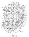
- FIG. 1illustrates a deposition valve assembly 10 having a mounting block 12 resting on an isolation unit 14 .
- Mounting block 12may be a typical valve assembly mounting device with an integral heater (not shown) for maintaining a steady temperature in the various valves.
- Mounting block 12also includes a first surface 16 for receiving one or more deposition valves 18 .
- Deposition valves 18may include an upper chamber 20 and a lower chamber 22 .
- the upper chambermay include a pneumatically actuated spring-biased apparatus controlling a bypass valve within lower chamber 22 for controlling fluid flow through each valve and the valve assembly as a unit.
- the spring biased apparatusis controlled by air flow through air inlet 24 .
- Isolation unit 14may include a rigid outer surface 26 composed of aluminum, stainless steel, or any other suitable material and an isolation sheet 28 composed of a high density foam or other suitable material. Isolation unit 14 is used to not only protect the valve assembly from damage due to shock or vibration, but also acts to thermally isolate the valve assembly and the remainder of the tool
- mounting block 12serves as a base unit for supporting the valve assembly while also providing heat to the valves.
- Valves 18are oriented at a right angle with respect to first surface 16 (or top surface in FIG. 1 ) and secured to the first surface with bolts 30 through cradles 32 .
- Cradles 32may be composed of aluminum, stainless steel, or any other suitable material and are generally u-shaped to permit fluid lines 34 to pass through the u-shaped openings 36 in cradles 32 as well as locate seals (not shown) between the fluid line interconnection and the valves 18 .
- Valve assembly 10may also include a manual adjustment valve 38 having an adjustment knob 40 which can be used as a needle valve to regulate flow throughout the valve assembly.
- Valve assembly 10may also include a pair of thermocouples 42 to measure the outer surface temperature of at least two valves.
- Thermocouples 42are connected to the respective valves with clamps 44 secured around valves 18 with bolts 46 .
- the thermocouples 42are connected to clamps 44 through thermocouple mounts 48 and the clamps may include through holes (not shown) which permit the thermocouple probes to be positioned directly adjacent or in contact with the valve 18 outer surfaces for more accurate temperature readings and temperature control.
- fluid lines 34may be composed of stainless steel or any other suitable material which is process, temperature, and pressure resistant. At several points along the length of fluid lines 34 junction boxes 50 may be utilized to fluidly connect two, three, four, or more fluid lines.
- a carrier or purge line inlet 52is positioned upstream from a carrier or purge line outlet 54 and a precursor or processing fluid inlet 56 . Further, a process vacuum inlet 58 may be located on the valve assembly.
- Carrier line inlet 52is in fluid communication with the precursor fluid inlets and permits the appropriate mixing of the carrier fluid and the precursor fluids.
- the carrier fluidmay be a nitrogen gas or an argon gas. After proper mixing within the valve assembly, the fluid exits valve assembly 10 at reactor outlet 60 and is directed to the reaction chamber for a deposition or etch process, as appropriate.
- FIG. 2illustrates deposition valve assembly 10 having a fluid line heating assembly 64 and an insulator assembly 66 mounted to valve assembly 10 .
- Fluid line heating assembly 64is preferably installed adjacent mounting block 12 and is used to assist in maintaining a consistent fluid temperature throughout the valve assembly and particularly as the carrier fluids and precursor fluids pass through the fluid lines 34 between each of the deposition valves 18 within the deposition valve assembly 10 .
- Insulator assembly 66may be positioned on the opposite side of fluid line heating assembly 64 from mounting block 12 to also assist in maintaining a consistent temperature throughout valve assembly 10 and fluid lines 34 .
- insulator assembly 66assists in maintaining a consistent temperature throughout deposition valve assembly by reducing heat loss radiating away from deposition valves 18 and fluid lines 34 .
- the insulator assemblyalso reduces the load on the various heating elements within the deposition valve assembly.
- FIG. 3illustrates an exploded view of fluid line heating assembly 64 removed from deposition valve assembly 10 .
- fluid line heating assembly 64may include a first fluid line heating unit 68 and a second fluid line heating unit 70 .
- Each of the first and second fluid line heating unitsmay be oriented to cover one-half of the deposition valve assembly 10 or any other suitable combination of the valve assembly so long fluid lines 34 are each covered by a fluid line heating unit to maintain the temperature therein.
- a top surface 72 of both first fluid line heating unit 68 and second fluid line heating unit 70may be smooth or flat to receive insulator assembly 66 and evenly maintain the fluid line heating assembly 64 temperature.
- each fluid line heating unitincludes a heating element 74 extending inward that can each be separately controlled from a remote location.
- the fluid line heating unitsmay also include a plurality of recessed portions 76 formed in a bottom surface 78 . As will be discussed in greater detail below, each recessed portion 76 is aligned to surround and positioned adjacent a fluid line 34 which is exposed or outside of a cradle 32 and/or deposition valves 18 .
- fluid line and fluidare used to encompass any liquid, gas, or solid and are not intended, nor should they be interpreted to limit the type, composition, or state of any liquid, solid, gas, or combination thereof that may be utilized within the spirit and scope of the disclosure and the claims.
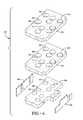
- FIG. 4illustrates an enlarged exploded view of insulator assembly 66 (or secondary insulator) having a first secondary insulator layer 80 , a second secondary insulator layer 82 , and third secondary insulator layer 84 .
- the insulator layersmay be separable from one another or secured together with an adhesive or other suitable fastening method.
- a first side support 86 and a second side support 88may be placed on opposing sidewalls of the insulator assembly 66 to assist with positioning and holding the insulator assembly in position.
- the first and second side supports 86 , 88may be composed of a metal, a sponge material (such as silicone foam), or any other suitable material known within the art as will be readily apparent.
- First secondary layer 80includes a plurality of apertures 90 strategically placed along a horizontal surface of the layer and extending throughout the full thickness of the first secondary layer.
- second secondary layer 82includes a plurality of apertures 92 extending throughout the thickness of the second secondary layer
- the third secondary layer 84includes a plurality of apertures 94 extending throughout the thickness of the third secondary layer.
- all three layers of the insulator assembly 66are aligned with one another and with respect to deposition valves 18 .
- the three secondary insulation layers 80 , 82 , and 84are each aligned to permit the apertures to surround the lower chamber 22 of each deposition valve 18 . Accordingly, this arrangement reduces heat loss to the surrounding environment.
- Secondary insulation layers 80 , 82 , and 84are each approximately 1 ⁇ 2′′ thick sponge or high density material, such as silicone foam. While the particular material and dimensions utilized are provided purely for this exemplary non-limiting embodiment, one of ordinary skill in the art will immediately realize that any suitable material and dimensions may be utilized without departing from the spirit and scope of the disclosure.
- Second insulating layer 96is shown installed between deposition valves 18 and specifically below fluid lines 34 .
- Second insulating layer 96may be composed of a high density foam, such as silicone foam, or any other suitable material that can assist in retaining heat while simultaneously acting as a seal.
- second insulating layer 96may be installed before deposition valves 18 and may be specially designed and oriented to the particular valve orientation located on mounting block 12 .
- any orientation or arrangement of deposition valves 18may be constructed and a similar second insulating layer 96 may be utilized.
- second insulating layer 96is shown and described as a single piece, any number of layers may be incorporated, including multiple layers stacked atop one another or various single layers abutting one another on mounting block 12 .
- second insulating layer 96is preferably dimensioned to fit below fluid lines 34 during operation.
- second insulating layer 96may be installed on mounting block 12 prior to cradles 32 and deposition valves 18 . Nevertheless, the second insulating layer 96 may be installed after the cradles 32 and deposition valves 18 in other embodiments. Regardless of when installed, second insulating layer 96 is preferably positioned just below fluid lines 34 when fully installed so as to provide a small air gap between fluid lines 34 and the second insulating layer 96 .
- first heating unit 68 and second heating unit 70are shown removed from the deposition valve assembly 10 .
- the first and second heating units 68 , 70include a plurality of recessed portions 76 which directly expose an intermediate layer 98 which may be an encapsulated rubber, such as silicone rubber or any other suitable material known in the art.
- each heating unitmay include a first substrate 100 , a third substrate 104 , and a second substrate 102 positioned between the first and third substrates.
- the substrates combinedalso include inner ends 106 which meet with respective inner ends from the other heating unit in this non-limiting example.
- the first and third substrates 100 and 104are each composed of a silicone or other high density foam, while the second substrate is a rubber, such as silicone rubber.
- the first and second heating units 68 , 70may be a single piece of high density foam with recessed portions 76 removed from the bottom surface 78 and heating element 74 exposed only at the top of the recessed portions, which may then be encapsulated with a silicone rubber or other suitable material.
- the recessed portions 76are oriented in both an X and Y plane as, in this particular non-limiting example; there are a plurality of fluid lines 34 which are exposed as they traverse both directions.
- Each labeled recessed portion 76provides heating to a fluid line 34 which includes at least a portion that is not located within a cradle 32 or below a deposition valve 18 .
- each recessed portionprovides direct radiant heat to a fluid line which would otherwise not be directly heated without the respective heating unit and heating element 74 . Accordingly, while the particular orientation and arrangement of the recessed portions is applicable to this non-limiting example, any number and orientation of recessed portions may be utilized to provide radiant or convection heating to the exposed fluid lines.
- each heating until 68 , 70may be modified or adapted based on the deposition valve orientation and positioning.
- three or four different heating unitsmay be utilized and may each include their own heating elements 74 disposed therein for heating the respective fluid lines 34 .
- a single heating unitmay be utilized and include only a single heating element 74 or a plurality of heating elements disposed throughout the heating unit.
- FIGS. 7 and 8illustrate assembled views of the deposition valve assembly with the heating units and various insulation layers in place.
- junction boxes 50as applicable, of the various fluid lines 34 may function to create gaps or spaces 108 around the remaining portions of fluid lines 34 .
- junction boxes 50may not be present and a generally rigid first and second heating units create the gaps or spaces 108 around fluid lines 34 .
- recessed portions 76 of heating unit 68 and 70are generally deep enough to create three sides (top side and two sidewalls) around each fluid line and extends less than completely around fluid lines 34 . Further, because the heating units 68 , 70 are resting adjacent and/or on second insulating layer 96 , the bottom side is occupied by the second insulating layer 96 . Accordingly, the recessed portions 76 of the heating units 68 , 70 together with the second insulating layer 96 effectively together surround each of the fluid lines 34 when fully assembled. As can be seen in FIG.
- heating element 74is positioned within second substrate 102 and provides radiant or convection heating to the fluid lines 34 during operation to maintain the fluid lines at the desired temperature, which can range from as low as room temperature up to 200 degrees C. or beyond.
- the air gaps between recessed portion 76 and second insulating layer 96permit the mounting block 12 with heating element (not shown) and the heating element 74 within the second substrate to heat the space and/or air directly surrounding the fluid line 34 to reduce hot spots on the fluid line 34 and provide for a more consistent precursor fluid and carrier fluid within the valve assembly.
- the valve assemblycan more efficiently and precisely transfer the precursor to the reaction chamber.
- a mounting block 12is provided with a heating element therein and the second insulating layer 96 may be installed thereon.
- a plurality of deposition valves 18 and fluid lines 34 interconnecting the deposition valves 18may be provided on mounting block 12 .
- An insulator unit 64may include installing a first heating unit 68 and potentially a second heating unit assembly 70 , each having a heating element 74 , over fluid lines 34 such that the heating units surround less than all of each of the fluid lines 34 with recessed portions 76 .
- the first and second heating units 68 , 70 in combination with the second insulating layer 96completely surround each fluid line 34 where recessed portions 76 are located.
- the heating elements 74are each separately controlled (i.e.
- heating element within first heating unit 68is separately controlled from heating element within second heating unit 70 ) in one aspect, or the heating elements may be actuated by a single controller, depending on the desired outcome. Still further, since at least one thermocouple 42 may be located within each zone covered by a heating unit, the controller for each heating unit 68 , 70 heating element 74 may be programmed to control the temperature at each thermocouple.
- the terms “comprises”, “comprising”, or any variation thereof,are intended to reference a non-exclusive inclusion, such that a process, method, article, composition or apparatus that comprises a list of elements does not include only those elements recited, but may also include other elements not expressly listed or inherent to such process, method, article, composition or apparatus.
- Other combinations and/or modifications of the above-described structures, arrangements, applications, proportions, elements, materials or components used in the practice of the present invention, in addition to those not specifically recited,may be varied or otherwise particularly adapted to specific environments, manufacturing specifications, design parameters or other operating requirements without departing from the general principles of the same.
Landscapes
- Chemical & Material Sciences (AREA)
- Engineering & Computer Science (AREA)
- Mechanical Engineering (AREA)
- General Engineering & Computer Science (AREA)
- General Chemical & Material Sciences (AREA)
- Chemical Kinetics & Catalysis (AREA)
- Materials Engineering (AREA)
- Metallurgy (AREA)
- Organic Chemistry (AREA)
- Details Of Valves (AREA)
- Valve Housings (AREA)
Abstract
Description
- This application claims priority to U.S. patent application Ser. No. 13/283,408 entitled “HEATER JACKET FOR A FLUID LINE” to Yednak III et al., filed on Oct. 27, 2011, the disclosure of which is hereby incorporated herein by reference in its entirety.
- This disclosure relates generally to semiconductor processing, and more particularly to a valve assembly having an improved temperature control system for semiconductor processing fluid lines.
- Semiconductor fabrication processes are typically conducted with the substrates supported within a chamber under controlled conditions. For many purposes, semiconductor substrates (e.g., wafers) are heated inside the process chamber. For example, substrates can be heated by direct physical contact with an internally heated wafer holder or “chuck.” “Susceptors” are wafer supports used in radiantly heated systems where the wafer and susceptors absorb radiant heat.
- Some of the important controlled conditions include, but are not limited to, fluid flow rate into the chamber, temperature of the reaction chamber, temperature of the fluid flowing into the reaction chamber, and temperature of the fluid throughout the fluid line.
- In order to obtain a consistent reaction environment, maintaining the correct flow rate of precursor at a correct temperature is among the key factors. However, the importance of maintaining the temperature of the precursors at a uniform temperature is not limited to just the reaction chamber. A number of precursors have a limited temperature range of gaseous phase composition. Thus, in order to maintain the correct flow rate, the precursor must be maintained within a slim temperature range from the source container, through the fluid line, and finally into the reaction chamber.
- A number of heater jackets have been developed in an attempt to maintain consistent fluid temperatures during the transition from the temperature controlled source container to the reaction chamber. One common example is cloth heater jackets which surround the fluid line and include a cloth inner layer in contact with the fluid line. The cloth heater jacket may be generally flexible but wear easily. An alternative to heater jackets includes heat tape, which is inexpensive but time consuming to install on fluid lines. Further, when a section of the fluid line needs to be worked on or replaced, the heat tape must be removed, scraped, and a new section installed in its place.
- Precursor valve assemblies also present a number of heating challenges due to their compact nature and exposed fluid line connections between each of the valve members or bodies.
- Various aspects and implementations are disclosed herein that relate to valve assembly designs and methods of heating a fluid line in a valve assembly. In one aspect, a valve assembly comprises a mounting block having a first surface, a plurality of valves connected to the mounting block first surface, at least one fluid line connecting the plurality of valves spaced apart from the mounting block first surface, a heating element spaced apart from the at least one fluid line and located within a first insulating layer, and wherein the first insulating layer extends less than completely around the at least one fluid line.
- In an implementation, the heating element may be positioned adjacent the at least one fluid line. The valve assembly may further include a second insulating layer spaced apart from the heating element and between the at least one fluid line and the mounting block first surface. The first insulating layer and the second insulating layer may together surround the at least one fluid line. The heating element may radiantly heat the at least one fluid line. The first insulating layer may further include a recessed portion positioned at each of the at least one fluid lines.
- The valve assembly may further include a second heating element separate from the heating element. The heating element may be encapsulated within a recessed portion of the first insulating layer. The recessed portion may be encapsulated with a silicone rubber. The first insulating layer may be positioned between the plurality of valves. The valve assembly may further include a secondary insulator positioned on the first insulating layer. The secondary insulator may include three separable layers. The secondary insulator may further include a plurality of apertures adapted to receive the plurality of valves. The first insulating layer may be composed of a high density foam. The first insulating layer may further include a first upper insulating layer and a second insulating layer. The first upper insulating layer may further include a first heating element and the second upper insulating layer may further include a second heating element. The first heating element and the second heating element may be configured to be separately controlled. The heating element may radiantly heat the at least one fluid line only within the recessed portion.
- In another aspect, a method of heating a fluid line in a valve assembly comprises the steps of providing a first insulating layer having a heating element spaced apart and surrounding less than all of the at least one fluid line, surrounding the at least one fluid line between the first insulating layer and the valve block, and powering the heating element to radiantly heat an area between the first insulating layer and the valve block and the at least one fluid line.
- In yet another aspect, a valve assembly includes a mounting block having a mounting surface, a plurality of valves connected to the mounting block mounting surface, at least one fluid line in fluid communication with the plurality of valves above the mounting block mounting surface, a heating element positioned above the at least one fluid line and located within an upper insulating layer, and wherein the upper insulating layer extends less than completely around the at least one fluid line.
- This Summary is provided to introduce a selection of concepts in a simplified form that are further described below in the Detailed Description. This Summary is not intended to identify key features or essential features of the claimed subject matter, nor is it intended to be used to limit the scope of the claimed subject matter. Furthermore, the claimed subject matter is not limited to implementations that solve any or all disadvantages noted in any part of this disclosure.
FIG. 1 is a perspective view of a valve assembly mounted on a heated valve block.FIG. 2 is a perspective view of a valve assembly according to an embodiment of the present disclosure.FIG. 3 is a perspective view of a partially exploded valve assembly according to an embodiment of the present disclosure.FIG. 4 is a perspective view of an exploded valve assembly secondary insulating layer according to an embodiment of the present disclosure.FIG. 5 is a perspective view of a pair of first insulating layers removed from the valve assembly according to an embodiment of the present disclosure.FIG. 6 is a perspective view of a partially exploded valve assembly first insulating layer of the valve assembly according to an embodiment of the present disclosure.FIG. 7 is a cross-sectional view of the valve assembly according to an embodiment of the present disclosure taken generally about line7-7 inFIG. 2 .FIG. 8 is a cross-sectional view of the valve assembly according to an embodiment of the present disclosure taken generally about line8-8 inFIG. 7 .- The present aspects and implementations may be described in terms of functional block components and various processing steps. Such functional blocks may be realized by any number of hardware or software components configured to perform the specified functions and achieve the various results. For example, the present aspects may employ various sensors, detectors, flow control devices, heaters, and the like, which may carry out a variety of functions. In addition, the present aspects and implementations may be practiced in conjunction with any number of processing methods, and the apparatus and systems described may employ any number of processing methods, and the apparatus and systems described are merely examples of applications of the invention.
FIG. 1 illustrates adeposition valve assembly 10 having amounting block 12 resting on anisolation unit 14.Mounting block 12 may be a typical valve assembly mounting device with an integral heater (not shown) for maintaining a steady temperature in the various valves.Mounting block 12 also includes afirst surface 16 for receiving one ormore deposition valves 18.Deposition valves 18 may include anupper chamber 20 and alower chamber 22. The upper chamber may include a pneumatically actuated spring-biased apparatus controlling a bypass valve withinlower chamber 22 for controlling fluid flow through each valve and the valve assembly as a unit. The spring biased apparatus is controlled by air flow throughair inlet 24.Isolation unit 14 may include a rigidouter surface 26 composed of aluminum, stainless steel, or any other suitable material and anisolation sheet 28 composed of a high density foam or other suitable material.Isolation unit 14 is used to not only protect the valve assembly from damage due to shock or vibration, but also acts to thermally isolate the valve assembly and the remainder of the tool- As discussed above, mounting
block 12 serves as a base unit for supporting the valve assembly while also providing heat to the valves.Valves 18 are oriented at a right angle with respect to first surface16 (or top surface inFIG. 1 ) and secured to the first surface withbolts 30 throughcradles 32.Cradles 32 may be composed of aluminum, stainless steel, or any other suitable material and are generally u-shaped to permitfluid lines 34 to pass through theu-shaped openings 36 incradles 32 as well as locate seals (not shown) between the fluid line interconnection and thevalves 18. Valve assembly 10 may also include amanual adjustment valve 38 having an adjustment knob40 which can be used as a needle valve to regulate flow throughout the valve assembly.Valve assembly 10 may also include a pair ofthermocouples 42 to measure the outer surface temperature of at least two valves.Thermocouples 42 are connected to the respective valves withclamps 44 secured aroundvalves 18 withbolts 46. Thethermocouples 42 are connected to clamps44 through thermocouple mounts48 and the clamps may include through holes (not shown) which permit the thermocouple probes to be positioned directly adjacent or in contact with thevalve 18 outer surfaces for more accurate temperature readings and temperature control.- Referring still to
FIG. 1 ,fluid lines 34 may be composed of stainless steel or any other suitable material which is process, temperature, and pressure resistant. At several points along the length offluid lines 34junction boxes 50 may be utilized to fluidly connect two, three, four, or more fluid lines. - A carrier or purge
line inlet 52 is positioned upstream from a carrier or purgeline outlet 54 and a precursor or processingfluid inlet 56. Further, aprocess vacuum inlet 58 may be located on the valve assembly.Carrier line inlet 52 is in fluid communication with the precursor fluid inlets and permits the appropriate mixing of the carrier fluid and the precursor fluids. In one non-limiting example, the carrier fluid may be a nitrogen gas or an argon gas. After proper mixing within the valve assembly, the fluid exitsvalve assembly 10 atreactor outlet 60 and is directed to the reaction chamber for a deposition or etch process, as appropriate. FIG. 2 illustratesdeposition valve assembly 10 having a fluidline heating assembly 64 and aninsulator assembly 66 mounted tovalve assembly 10. Fluidline heating assembly 64 is preferably installedadjacent mounting block 12 and is used to assist in maintaining a consistent fluid temperature throughout the valve assembly and particularly as the carrier fluids and precursor fluids pass through thefluid lines 34 between each of thedeposition valves 18 within thedeposition valve assembly 10.Insulator assembly 66 may be positioned on the opposite side of fluidline heating assembly 64 from mountingblock 12 to also assist in maintaining a consistent temperature throughoutvalve assembly 10 and fluid lines34. Specifically,insulator assembly 66 assists in maintaining a consistent temperature throughout deposition valve assembly by reducing heat loss radiating away fromdeposition valves 18 and fluid lines34. Not only doesinsulator assembly 66 reduce heat loss within the valve assembly, the insulator assembly also reduces the load on the various heating elements within the deposition valve assembly.FIG. 3 illustrates an exploded view of fluidline heating assembly 64 removed fromdeposition valve assembly 10. In one aspect, fluidline heating assembly 64 may include a first fluidline heating unit 68 and a second fluidline heating unit 70. Each of the first and second fluid line heating units may be oriented to cover one-half of thedeposition valve assembly 10 or any other suitable combination of the valve assembly solong fluid lines 34 are each covered by a fluid line heating unit to maintain the temperature therein.- As can be further seen in
FIG. 3 , atop surface 72 of both first fluidline heating unit 68 and second fluidline heating unit 70 may be smooth or flat to receiveinsulator assembly 66 and evenly maintain the fluidline heating assembly 64 temperature. Further, each fluid line heating unit includes aheating element 74 extending inward that can each be separately controlled from a remote location. The fluid line heating units may also include a plurality of recessedportions 76 formed in abottom surface 78. As will be discussed in greater detail below, each recessedportion 76 is aligned to surround and positioned adjacent afluid line 34 which is exposed or outside of acradle 32 and/ordeposition valves 18. Throughout this detailed description, the term fluid line and fluid are used to encompass any liquid, gas, or solid and are not intended, nor should they be interpreted to limit the type, composition, or state of any liquid, solid, gas, or combination thereof that may be utilized within the spirit and scope of the disclosure and the claims. FIG. 4 illustrates an enlarged exploded view of insulator assembly66 (or secondary insulator) having a firstsecondary insulator layer 80, a secondsecondary insulator layer 82, and thirdsecondary insulator layer 84. The insulator layers may be separable from one another or secured together with an adhesive or other suitable fastening method. Afirst side support 86 and asecond side support 88 may be placed on opposing sidewalls of theinsulator assembly 66 to assist with positioning and holding the insulator assembly in position. The first and second side supports86,88 may be composed of a metal, a sponge material (such as silicone foam), or any other suitable material known within the art as will be readily apparent.- First
secondary layer 80 includes a plurality ofapertures 90 strategically placed along a horizontal surface of the layer and extending throughout the full thickness of the first secondary layer. Similarly, secondsecondary layer 82 includes a plurality ofapertures 92 extending throughout the thickness of the second secondary layer and the thirdsecondary layer 84 includes a plurality ofapertures 94 extending throughout the thickness of the third secondary layer. Advantageously, all three layers of theinsulator assembly 66 are aligned with one another and with respect todeposition valves 18. The three secondary insulation layers80,82, and84 are each aligned to permit the apertures to surround thelower chamber 22 of eachdeposition valve 18. Accordingly, this arrangement reduces heat loss to the surrounding environment. - Secondary insulation layers80,82, and84 are each approximately ½″ thick sponge or high density material, such as silicone foam. While the particular material and dimensions utilized are provided purely for this exemplary non-limiting embodiment, one of ordinary skill in the art will immediately realize that any suitable material and dimensions may be utilized without departing from the spirit and scope of the disclosure.
- Referring now to
FIG. 3 , a second insulatinglayer 96 is shown installed betweendeposition valves 18 and specifically below fluid lines34. Second insulatinglayer 96 may be composed of a high density foam, such as silicone foam, or any other suitable material that can assist in retaining heat while simultaneously acting as a seal. In operation, second insulatinglayer 96 may be installed beforedeposition valves 18 and may be specially designed and oriented to the particular valve orientation located on mountingblock 12. Thus it is seen that any orientation or arrangement ofdeposition valves 18 may be constructed and a similar second insulatinglayer 96 may be utilized. Further, although second insulatinglayer 96 is shown and described as a single piece, any number of layers may be incorporated, including multiple layers stacked atop one another or various single layers abutting one another on mountingblock 12. - Still further, second insulating
layer 96 is preferably dimensioned to fit belowfluid lines 34 during operation. In many embodiments, second insulatinglayer 96 may be installed on mountingblock 12 prior tocradles 32 anddeposition valves 18. Nevertheless, the second insulatinglayer 96 may be installed after thecradles 32 anddeposition valves 18 in other embodiments. Regardless of when installed, second insulatinglayer 96 is preferably positioned just belowfluid lines 34 when fully installed so as to provide a small air gap betweenfluid lines 34 and the second insulatinglayer 96. - Referring now to
FIGS. 5 and 6 ,first heating unit 68 andsecond heating unit 70 are shown removed from thedeposition valve assembly 10. As can be better seen in these two views, the first andsecond heating units portions 76 which directly expose anintermediate layer 98 which may be an encapsulated rubber, such as silicone rubber or any other suitable material known in the art. In one aspect, each heating unit may include afirst substrate 100, athird substrate 104, and asecond substrate 102 positioned between the first and third substrates. The substrates combined also includeinner ends 106 which meet with respective inner ends from the other heating unit in this non-limiting example. In one non-limiting example, the first andthird substrates second heating units portions 76 removed from thebottom surface 78 andheating element 74 exposed only at the top of the recessed portions, which may then be encapsulated with a silicone rubber or other suitable material. The proposed examples are purely for the purpose of explaining the scope and breadth of the disclosure and are in no way to be viewed as limiting the claims. - Further, the recessed
portions 76 are oriented in both an X and Y plane as, in this particular non-limiting example; there are a plurality offluid lines 34 which are exposed as they traverse both directions. Each labeled recessedportion 76 provides heating to afluid line 34 which includes at least a portion that is not located within acradle 32 or below adeposition valve 18. For the sake of clarity, each recessed portion provides direct radiant heat to a fluid line which would otherwise not be directly heated without the respective heating unit andheating element 74. Accordingly, while the particular orientation and arrangement of the recessed portions is applicable to this non-limiting example, any number and orientation of recessed portions may be utilized to provide radiant or convection heating to the exposed fluid lines. Further, the shape and positioning of each heating until68,70 may be modified or adapted based on the deposition valve orientation and positioning. For example, three or four different heating units may be utilized and may each include theirown heating elements 74 disposed therein for heating the respective fluid lines34. Further, a single heating unit may be utilized and include only asingle heating element 74 or a plurality of heating elements disposed throughout the heating unit. FIGS. 7 and 8 illustrate assembled views of the deposition valve assembly with the heating units and various insulation layers in place. As particularly seen inFIG. 7 ,junction boxes 50, as applicable, of thevarious fluid lines 34 may function to create gaps orspaces 108 around the remaining portions of fluid lines34. In another implementation,junction boxes 50 may not be present and a generally rigid first and second heating units create the gaps orspaces 108 aroundfluid lines 34.- In one non-limiting example, recessed
portions 76 ofheating unit fluid lines 34. Further, because theheating units layer 96, the bottom side is occupied by the second insulatinglayer 96. Accordingly, the recessedportions 76 of theheating units layer 96 effectively together surround each of thefluid lines 34 when fully assembled. As can be seen inFIG. 8 ,heating element 74 is positioned withinsecond substrate 102 and provides radiant or convection heating to thefluid lines 34 during operation to maintain the fluid lines at the desired temperature, which can range from as low as room temperature up to 200 degrees C. or beyond. Specifically, the air gaps between recessedportion 76 and second insulatinglayer 96 permit the mountingblock 12 with heating element (not shown) and theheating element 74 within the second substrate to heat the space and/or air directly surrounding thefluid line 34 to reduce hot spots on thefluid line 34 and provide for a more consistent precursor fluid and carrier fluid within the valve assembly. Thus, the valve assembly can more efficiently and precisely transfer the precursor to the reaction chamber. - As discussed above, in one non-limiting example, a mounting
block 12 is provided with a heating element therein and the second insulatinglayer 96 may be installed thereon. A plurality ofdeposition valves 18 andfluid lines 34 interconnecting thedeposition valves 18 may be provided on mountingblock 12. Aninsulator unit 64 may include installing afirst heating unit 68 and potentially a secondheating unit assembly 70, each having aheating element 74, overfluid lines 34 such that the heating units surround less than all of each of thefluid lines 34 with recessedportions 76. Once fully installed, the first andsecond heating units layer 96 completely surround eachfluid line 34 where recessedportions 76 are located. Theheating elements 74 are each separately controlled (i.e. heating element withinfirst heating unit 68 is separately controlled from heating element within second heating unit70) in one aspect, or the heating elements may be actuated by a single controller, depending on the desired outcome. Still further, since at least onethermocouple 42 may be located within each zone covered by a heating unit, the controller for eachheating unit heating element 74 may be programmed to control the temperature at each thermocouple. The above discussion is merely exemplary and a person of skill in the art will immediately recognize that a variety of modifications can be achieved without departing from the spirit and scope of the detailed description. - These and other embodiments for methods and apparatus for a valve assembly to maintain efficient heating may incorporate concepts, embodiments, and configurations as described with respect to embodiments of apparatus for valve assemblies described above. The particular implementations shown and described are illustrative of the invention and its best mode and are not intended to otherwise limit the scope of the aspects and implementations in any way. Indeed, for the sake of brevity, conventional manufacturing, connection, preparation, and other functional aspects of the system may not be described in detail. Furthermore, the connecting lines shown in the various figures are intended to represent exemplary functional relationships and/or physical couplings between the various elements. Many alternative or additional functional relationship or physical connections may be present in the practical system, and/or may be absent in some embodiments.
- As used herein, the terms “comprises”, “comprising”, or any variation thereof, are intended to reference a non-exclusive inclusion, such that a process, method, article, composition or apparatus that comprises a list of elements does not include only those elements recited, but may also include other elements not expressly listed or inherent to such process, method, article, composition or apparatus. Other combinations and/or modifications of the above-described structures, arrangements, applications, proportions, elements, materials or components used in the practice of the present invention, in addition to those not specifically recited, may be varied or otherwise particularly adapted to specific environments, manufacturing specifications, design parameters or other operating requirements without departing from the general principles of the same.
Claims (20)
1. A valve assembly comprising:
a mounting block having a first surface;
a plurality of valves connected to the mounting block first surface;
at least one fluid line connecting the plurality of valves spaced apart from the mounting block first surface;
a heating element spaced apart from the at least one fluid line and located within a first insulating layer; and,
wherein the first insulating layer extends less than completely around the at least one fluid line.
2. The valve assembly ofclaim 1 wherein the heating element is positioned adjacent the at least one fluid line.
3. The valve assembly ofclaim 1 further comprising a second insulating layer spaced apart from the heating element and between the at least one fluid line and the mounting block first surface.
4. The valve assembly ofclaim 3 wherein the first insulating layer and the second insulating layer together surround the at least one fluid line.
5. The valve assembly ofclaim 5 wherein the heating element radiantly heats the at least one fluid line.
6. The valve assembly ofclaim 1 wherein the first insulating layer further comprises a recessed portion positioned at each of the at least one fluid lines.
7. The valve assembly ofclaim 1 further comprising a second heating element separate from the heating element.
8. The valve assembly ofclaim 1 wherein the heating element is encapsulated within a recessed portion of the first insulating layer.
9. The valve assembly ofclaim 8 wherein the recessed portion is encapsulated with a silicone rubber.
10. The valve assembly ofclaim 1 wherein the first insulating layer is positioned between the plurality of valves.
11. The valve assembly ofclaim 10 further comprising a secondary insulator positioned on the first insulating layer.
12. The valve assembly ofclaim 11 wherein the secondary insulator comprises three separable layers.
13. The valve assembly ofclaim 12 wherein the secondary insulator further comprises a plurality of apertures adapted to receive the plurality of valves.
14. The valve assembly ofclaim 1 wherein the first insulating layer is composed of a high density foam.
15. The valve assembly ofclaim 1 wherein the first insulating layer further comprises a first upper insulating layer and a second upper insulating layer.
16. The valve assembly ofclaim 15 wherein the first upper insulating layer further comprises a first heating element and the second upper insulating layer further comprises a second heating element.
17. The valve assembly ofclaim 16 wherein the first heating element and the second heating element are configured to be separately controlled.
18. The valve assembly ofclaim 1 wherein the heating element radiantly heats the at least one fluid line only within the recessed portion.
19. A method of heating a fluid line in a valve assembly comprising the steps of:
providing a valve block having a first surface with a plurality of valves and at least one fluid line interconnecting the plurality of valves;
providing a first insulating layer having a heating element spaced apart and surrounding less than all of the at least one fluid line;
surrounding the at least one fluid line between the first insulating layer and the valve block; and,
powering the heating element to radiantly heat an area between the first insulating layer and the valve block and the at least one fluid line.
20. A valve assembly comprising:
a mounting block having a mounting surface;
a plurality of valves connected to the mounting block mounting surface;
at least one fluid line in fluid communication with the plurality of valves above the mounting block mounting surface;
a heating element positioned above the at least one fluid line and located within an upper insulating layer; and,
wherein the upper insulating layer extends less than completely around the at least one fluid line.
Priority Applications (1)
| Application Number | Priority Date | Filing Date | Title |
|---|---|---|---|
| US13/312,591US9096931B2 (en) | 2011-10-27 | 2011-12-06 | Deposition valve assembly and method of heating the same |
Applications Claiming Priority (2)
| Application Number | Priority Date | Filing Date | Title |
|---|---|---|---|
| US13/283,408US9341296B2 (en) | 2011-10-27 | 2011-10-27 | Heater jacket for a fluid line |
| US13/312,591US9096931B2 (en) | 2011-10-27 | 2011-12-06 | Deposition valve assembly and method of heating the same |
Related Parent Applications (1)
| Application Number | Title | Priority Date | Filing Date |
|---|---|---|---|
| US13/283,408Continuation-In-PartUS9341296B2 (en) | 2011-10-27 | 2011-10-27 | Heater jacket for a fluid line |
Publications (2)
| Publication Number | Publication Date |
|---|---|
| US20130104992A1true US20130104992A1 (en) | 2013-05-02 |
| US9096931B2 US9096931B2 (en) | 2015-08-04 |
Family
ID=48171169
Family Applications (1)
| Application Number | Title | Priority Date | Filing Date |
|---|---|---|---|
| US13/312,591Active2032-05-22US9096931B2 (en) | 2011-10-27 | 2011-12-06 | Deposition valve assembly and method of heating the same |
Country Status (1)
| Country | Link |
|---|---|
| US (1) | US9096931B2 (en) |
Cited By (407)
| Publication number | Priority date | Publication date | Assignee | Title |
|---|---|---|---|---|
| US20100322604A1 (en)* | 2006-10-10 | 2010-12-23 | Kyle Fondurulia | Precursor delivery system |
| US20110070380A1 (en)* | 2009-08-14 | 2011-03-24 | Eric Shero | Systems and methods for thin-film deposition of metal oxides using excited nitrogen-oxygen species |
| US8877655B2 (en) | 2010-05-07 | 2014-11-04 | Asm America, Inc. | Systems and methods for thin-film deposition of metal oxides using excited nitrogen-oxygen species |
| US8894870B2 (en) | 2013-02-01 | 2014-11-25 | Asm Ip Holding B.V. | Multi-step method and apparatus for etching compounds containing a metal |
| US8933375B2 (en) | 2012-06-27 | 2015-01-13 | Asm Ip Holding B.V. | Susceptor heater and method of heating a substrate |
| US8946830B2 (en) | 2012-04-04 | 2015-02-03 | Asm Ip Holdings B.V. | Metal oxide protective layer for a semiconductor device |
| US8993054B2 (en) | 2013-07-12 | 2015-03-31 | Asm Ip Holding B.V. | Method and system to reduce outgassing in a reaction chamber |
| US9005539B2 (en) | 2011-11-23 | 2015-04-14 | Asm Ip Holding B.V. | Chamber sealing member |
| US9017481B1 (en) | 2011-10-28 | 2015-04-28 | Asm America, Inc. | Process feed management for semiconductor substrate processing |
| US9018111B2 (en) | 2013-07-22 | 2015-04-28 | Asm Ip Holding B.V. | Semiconductor reaction chamber with plasma capabilities |
| US9021985B2 (en) | 2012-09-12 | 2015-05-05 | Asm Ip Holdings B.V. | Process gas management for an inductively-coupled plasma deposition reactor |
| US9029253B2 (en) | 2012-05-02 | 2015-05-12 | Asm Ip Holding B.V. | Phase-stabilized thin films, structures and devices including the thin films, and methods of forming same |
| US9117866B2 (en) | 2012-07-31 | 2015-08-25 | Asm Ip Holding B.V. | Apparatus and method for calculating a wafer position in a processing chamber under process conditions |
| US9167625B2 (en) | 2011-11-23 | 2015-10-20 | Asm Ip Holding B.V. | Radiation shielding for a substrate holder |
| US9169975B2 (en) | 2012-08-28 | 2015-10-27 | Asm Ip Holding B.V. | Systems and methods for mass flow controller verification |
| US9177784B2 (en) | 2012-05-07 | 2015-11-03 | Asm Ip Holdings B.V. | Semiconductor device dielectric interface layer |
| US9202727B2 (en) | 2012-03-02 | 2015-12-01 | ASM IP Holding | Susceptor heater shim |
| US9240412B2 (en) | 2013-09-27 | 2016-01-19 | Asm Ip Holding B.V. | Semiconductor structure and device and methods of forming same using selective epitaxial process |
| US9324811B2 (en) | 2012-09-26 | 2016-04-26 | Asm Ip Holding B.V. | Structures and devices including a tensile-stressed silicon arsenic layer and methods of forming same |
| US9341296B2 (en) | 2011-10-27 | 2016-05-17 | Asm America, Inc. | Heater jacket for a fluid line |
| US9394608B2 (en) | 2009-04-06 | 2016-07-19 | Asm America, Inc. | Semiconductor processing reactor and components thereof |
| US9396934B2 (en) | 2013-08-14 | 2016-07-19 | Asm Ip Holding B.V. | Methods of forming films including germanium tin and structures and devices including the films |
| US9404587B2 (en) | 2014-04-24 | 2016-08-02 | ASM IP Holding B.V | Lockout tagout for semiconductor vacuum valve |
| US9447498B2 (en) | 2014-03-18 | 2016-09-20 | Asm Ip Holding B.V. | Method for performing uniform processing in gas system-sharing multiple reaction chambers |
| US9455138B1 (en) | 2015-11-10 | 2016-09-27 | Asm Ip Holding B.V. | Method for forming dielectric film in trenches by PEALD using H-containing gas |
| US9478415B2 (en) | 2015-02-13 | 2016-10-25 | Asm Ip Holding B.V. | Method for forming film having low resistance and shallow junction depth |
| US9484191B2 (en) | 2013-03-08 | 2016-11-01 | Asm Ip Holding B.V. | Pulsed remote plasma method and system |
| CN106164555A (en)* | 2014-10-29 | 2016-11-23 | 株式会社富士金 | Fluid control heater and fluid control device |
| US9543180B2 (en) | 2014-08-01 | 2017-01-10 | Asm Ip Holding B.V. | Apparatus and method for transporting wafers between wafer carrier and process tool under vacuum |
| US9556516B2 (en) | 2013-10-09 | 2017-01-31 | ASM IP Holding B.V | Method for forming Ti-containing film by PEALD using TDMAT or TDEAT |
| US9558931B2 (en) | 2012-07-27 | 2017-01-31 | Asm Ip Holding B.V. | System and method for gas-phase sulfur passivation of a semiconductor surface |
| US9589770B2 (en) | 2013-03-08 | 2017-03-07 | Asm Ip Holding B.V. | Method and systems for in-situ formation of intermediate reactive species |
| US9605343B2 (en) | 2013-11-13 | 2017-03-28 | Asm Ip Holding B.V. | Method for forming conformal carbon films, structures conformal carbon film, and system of forming same |
| US9607837B1 (en) | 2015-12-21 | 2017-03-28 | Asm Ip Holding B.V. | Method for forming silicon oxide cap layer for solid state diffusion process |
| US9627221B1 (en) | 2015-12-28 | 2017-04-18 | Asm Ip Holding B.V. | Continuous process incorporating atomic layer etching |
| US9640416B2 (en) | 2012-12-26 | 2017-05-02 | Asm Ip Holding B.V. | Single-and dual-chamber module-attachable wafer-handling chamber |
| US9647114B2 (en) | 2015-08-14 | 2017-05-09 | Asm Ip Holding B.V. | Methods of forming highly p-type doped germanium tin films and structures and devices including the films |
| US9657845B2 (en) | 2014-10-07 | 2017-05-23 | Asm Ip Holding B.V. | Variable conductance gas distribution apparatus and method |
| US9659799B2 (en) | 2012-08-28 | 2017-05-23 | Asm Ip Holding B.V. | Systems and methods for dynamic semiconductor process scheduling |
| US9711345B2 (en) | 2015-08-25 | 2017-07-18 | Asm Ip Holding B.V. | Method for forming aluminum nitride-based film by PEALD |
| US9735024B2 (en) | 2015-12-28 | 2017-08-15 | Asm Ip Holding B.V. | Method of atomic layer etching using functional group-containing fluorocarbon |
| US9754779B1 (en) | 2016-02-19 | 2017-09-05 | Asm Ip Holding B.V. | Method for forming silicon nitride film selectively on sidewalls or flat surfaces of trenches |
| US9793115B2 (en) | 2013-08-14 | 2017-10-17 | Asm Ip Holding B.V. | Structures and devices including germanium-tin films and methods of forming same |
| US9793135B1 (en) | 2016-07-14 | 2017-10-17 | ASM IP Holding B.V | Method of cyclic dry etching using etchant film |
| US9793148B2 (en) | 2011-06-22 | 2017-10-17 | Asm Japan K.K. | Method for positioning wafers in multiple wafer transport |
| US9812320B1 (en) | 2016-07-28 | 2017-11-07 | Asm Ip Holding B.V. | Method and apparatus for filling a gap |
| US9859151B1 (en) | 2016-07-08 | 2018-01-02 | Asm Ip Holding B.V. | Selective film deposition method to form air gaps |
| US9887082B1 (en) | 2016-07-28 | 2018-02-06 | Asm Ip Holding B.V. | Method and apparatus for filling a gap |
| US9891521B2 (en) | 2014-11-19 | 2018-02-13 | Asm Ip Holding B.V. | Method for depositing thin film |
| US9890456B2 (en) | 2014-08-21 | 2018-02-13 | Asm Ip Holding B.V. | Method and system for in situ formation of gas-phase compounds |
| US9899405B2 (en) | 2014-12-22 | 2018-02-20 | Asm Ip Holding B.V. | Semiconductor device and manufacturing method thereof |
| US9899291B2 (en) | 2015-07-13 | 2018-02-20 | Asm Ip Holding B.V. | Method for protecting layer by forming hydrocarbon-based extremely thin film |
| US9905420B2 (en) | 2015-12-01 | 2018-02-27 | Asm Ip Holding B.V. | Methods of forming silicon germanium tin films and structures and devices including the films |
| US9909214B2 (en) | 2015-10-15 | 2018-03-06 | Asm Ip Holding B.V. | Method for depositing dielectric film in trenches by PEALD |
| US9916980B1 (en) | 2016-12-15 | 2018-03-13 | Asm Ip Holding B.V. | Method of forming a structure on a substrate |
| US9960072B2 (en) | 2015-09-29 | 2018-05-01 | Asm Ip Holding B.V. | Variable adjustment for precise matching of multiple chamber cavity housings |
| US10032628B2 (en) | 2016-05-02 | 2018-07-24 | Asm Ip Holding B.V. | Source/drain performance through conformal solid state doping |
| US10043661B2 (en) | 2015-07-13 | 2018-08-07 | Asm Ip Holding B.V. | Method for protecting layer by forming hydrocarbon-based extremely thin film |
| US10083836B2 (en) | 2015-07-24 | 2018-09-25 | Asm Ip Holding B.V. | Formation of boron-doped titanium metal films with high work function |
| US10087525B2 (en) | 2015-08-04 | 2018-10-02 | Asm Ip Holding B.V. | Variable gap hard stop design |
| US10090316B2 (en) | 2016-09-01 | 2018-10-02 | Asm Ip Holding B.V. | 3D stacked multilayer semiconductor memory using doped select transistor channel |
| US10087522B2 (en) | 2016-04-21 | 2018-10-02 | Asm Ip Holding B.V. | Deposition of metal borides |
| USD830981S1 (en) | 2017-04-07 | 2018-10-16 | Asm Ip Holding B.V. | Susceptor for semiconductor substrate processing apparatus |
| US10103040B1 (en) | 2017-03-31 | 2018-10-16 | Asm Ip Holding B.V. | Apparatus and method for manufacturing a semiconductor device |
| US20180312279A1 (en)* | 2017-04-26 | 2018-11-01 | Marotta Controls, Inc. | Electronic pressure regulation system with proportional control valve |
| US10134757B2 (en) | 2016-11-07 | 2018-11-20 | Asm Ip Holding B.V. | Method of processing a substrate and a device manufactured by using the method |
| US10167557B2 (en) | 2014-03-18 | 2019-01-01 | Asm Ip Holding B.V. | Gas distribution system, reactor including the system, and methods of using the same |
| US10177025B2 (en) | 2016-07-28 | 2019-01-08 | Asm Ip Holding B.V. | Method and apparatus for filling a gap |
| US10179947B2 (en) | 2013-11-26 | 2019-01-15 | Asm Ip Holding B.V. | Method for forming conformal nitrided, oxidized, or carbonized dielectric film by atomic layer deposition |
| US10190213B2 (en) | 2016-04-21 | 2019-01-29 | Asm Ip Holding B.V. | Deposition of metal borides |
| US10211308B2 (en) | 2015-10-21 | 2019-02-19 | Asm Ip Holding B.V. | NbMC layers |
| US10229833B2 (en) | 2016-11-01 | 2019-03-12 | Asm Ip Holding B.V. | Methods for forming a transition metal nitride film on a substrate by atomic layer deposition and related semiconductor device structures |
| US10236177B1 (en) | 2017-08-22 | 2019-03-19 | ASM IP Holding B.V.. | Methods for depositing a doped germanium tin semiconductor and related semiconductor device structures |
| US10249524B2 (en) | 2017-08-09 | 2019-04-02 | Asm Ip Holding B.V. | Cassette holder assembly for a substrate cassette and holding member for use in such assembly |
| US10249577B2 (en) | 2016-05-17 | 2019-04-02 | Asm Ip Holding B.V. | Method of forming metal interconnection and method of fabricating semiconductor apparatus using the method |
| US10262859B2 (en) | 2016-03-24 | 2019-04-16 | Asm Ip Holding B.V. | Process for forming a film on a substrate using multi-port injection assemblies |
| US20190112707A1 (en)* | 2017-10-16 | 2019-04-18 | Asm Ip Holding B.V. | Systems and methods for atomic layer deposition |
| US10269558B2 (en) | 2016-12-22 | 2019-04-23 | Asm Ip Holding B.V. | Method of forming a structure on a substrate |
| US10276355B2 (en) | 2015-03-12 | 2019-04-30 | Asm Ip Holding B.V. | Multi-zone reactor, system including the reactor, and method of using the same |
| US10283353B2 (en) | 2017-03-29 | 2019-05-07 | Asm Ip Holding B.V. | Method of reforming insulating film deposited on substrate with recess pattern |
| US10290508B1 (en) | 2017-12-05 | 2019-05-14 | Asm Ip Holding B.V. | Method for forming vertical spacers for spacer-defined patterning |
| US10312055B2 (en) | 2017-07-26 | 2019-06-04 | Asm Ip Holding B.V. | Method of depositing film by PEALD using negative bias |
| US10319588B2 (en) | 2017-10-10 | 2019-06-11 | Asm Ip Holding B.V. | Method for depositing a metal chalcogenide on a substrate by cyclical deposition |
| US10322384B2 (en) | 2015-11-09 | 2019-06-18 | Asm Ip Holding B.V. | Counter flow mixer for process chamber |
| US10340135B2 (en) | 2016-11-28 | 2019-07-02 | Asm Ip Holding B.V. | Method of topologically restricted plasma-enhanced cyclic deposition of silicon or metal nitride |
| US10343920B2 (en) | 2016-03-18 | 2019-07-09 | Asm Ip Holding B.V. | Aligned carbon nanotubes |
| US10364496B2 (en) | 2011-06-27 | 2019-07-30 | Asm Ip Holding B.V. | Dual section module having shared and unshared mass flow controllers |
| US10367080B2 (en) | 2016-05-02 | 2019-07-30 | Asm Ip Holding B.V. | Method of forming a germanium oxynitride film |
| US10378106B2 (en) | 2008-11-14 | 2019-08-13 | Asm Ip Holding B.V. | Method of forming insulation film by modified PEALD |
| US10381226B2 (en) | 2016-07-27 | 2019-08-13 | Asm Ip Holding B.V. | Method of processing substrate |
| US10381219B1 (en) | 2018-10-25 | 2019-08-13 | Asm Ip Holding B.V. | Methods for forming a silicon nitride film |
| US10388513B1 (en) | 2018-07-03 | 2019-08-20 | Asm Ip Holding B.V. | Method for depositing silicon-free carbon-containing film as gap-fill layer by pulse plasma-assisted deposition |
| US10388509B2 (en) | 2016-06-28 | 2019-08-20 | Asm Ip Holding B.V. | Formation of epitaxial layers via dislocation filtering |
| US10395919B2 (en) | 2016-07-28 | 2019-08-27 | Asm Ip Holding B.V. | Method and apparatus for filling a gap |
| US10403504B2 (en) | 2017-10-05 | 2019-09-03 | Asm Ip Holding B.V. | Method for selectively depositing a metallic film on a substrate |
| US10410943B2 (en) | 2016-10-13 | 2019-09-10 | Asm Ip Holding B.V. | Method for passivating a surface of a semiconductor and related systems |
| US10435790B2 (en) | 2016-11-01 | 2019-10-08 | Asm Ip Holding B.V. | Method of subatmospheric plasma-enhanced ALD using capacitively coupled electrodes with narrow gap |
| US10446393B2 (en) | 2017-05-08 | 2019-10-15 | Asm Ip Holding B.V. | Methods for forming silicon-containing epitaxial layers and related semiconductor device structures |
| US10458018B2 (en) | 2015-06-26 | 2019-10-29 | Asm Ip Holding B.V. | Structures including metal carbide material, devices including the structures, and methods of forming same |
| US10468261B2 (en) | 2017-02-15 | 2019-11-05 | Asm Ip Holding B.V. | Methods for forming a metallic film on a substrate by cyclical deposition and related semiconductor device structures |
| US10468251B2 (en) | 2016-02-19 | 2019-11-05 | Asm Ip Holding B.V. | Method for forming spacers using silicon nitride film for spacer-defined multiple patterning |
| US10483099B1 (en) | 2018-07-26 | 2019-11-19 | Asm Ip Holding B.V. | Method for forming thermally stable organosilicon polymer film |
| US10504742B2 (en) | 2017-05-31 | 2019-12-10 | Asm Ip Holding B.V. | Method of atomic layer etching using hydrogen plasma |
| US10501866B2 (en) | 2016-03-09 | 2019-12-10 | Asm Ip Holding B.V. | Gas distribution apparatus for improved film uniformity in an epitaxial system |
| US10510536B2 (en) | 2018-03-29 | 2019-12-17 | Asm Ip Holding B.V. | Method of depositing a co-doped polysilicon film on a surface of a substrate within a reaction chamber |
| US10529554B2 (en) | 2016-02-19 | 2020-01-07 | Asm Ip Holding B.V. | Method for forming silicon nitride film selectively on sidewalls or flat surfaces of trenches |
| US10529542B2 (en) | 2015-03-11 | 2020-01-07 | Asm Ip Holdings B.V. | Cross-flow reactor and method |
| US10529563B2 (en) | 2017-03-29 | 2020-01-07 | Asm Ip Holdings B.V. | Method for forming doped metal oxide films on a substrate by cyclical deposition and related semiconductor device structures |
| US10535516B2 (en) | 2018-02-01 | 2020-01-14 | Asm Ip Holdings B.V. | Method for depositing a semiconductor structure on a surface of a substrate and related semiconductor structures |
| US10541333B2 (en) | 2017-07-19 | 2020-01-21 | Asm Ip Holding B.V. | Method for depositing a group IV semiconductor and related semiconductor device structures |
| US10559458B1 (en) | 2018-11-26 | 2020-02-11 | Asm Ip Holding B.V. | Method of forming oxynitride film |
| US10590535B2 (en) | 2017-07-26 | 2020-03-17 | Asm Ip Holdings B.V. | Chemical treatment, deposition and/or infiltration apparatus and method for using the same |
| US10600673B2 (en) | 2015-07-07 | 2020-03-24 | Asm Ip Holding B.V. | Magnetic susceptor to baseplate seal |
| US10607895B2 (en) | 2017-09-18 | 2020-03-31 | Asm Ip Holdings B.V. | Method for forming a semiconductor device structure comprising a gate fill metal |
| US10605530B2 (en) | 2017-07-26 | 2020-03-31 | Asm Ip Holding B.V. | Assembly of a liner and a flange for a vertical furnace as well as the liner and the vertical furnace |
| US10612137B2 (en) | 2016-07-08 | 2020-04-07 | Asm Ip Holdings B.V. | Organic reactants for atomic layer deposition |
| USD880437S1 (en) | 2018-02-01 | 2020-04-07 | Asm Ip Holding B.V. | Gas supply plate for semiconductor manufacturing apparatus |
| US10612136B2 (en) | 2018-06-29 | 2020-04-07 | ASM IP Holding, B.V. | Temperature-controlled flange and reactor system including same |
| US10643904B2 (en) | 2016-11-01 | 2020-05-05 | Asm Ip Holdings B.V. | Methods for forming a semiconductor device and related semiconductor device structures |
| US10643826B2 (en) | 2016-10-26 | 2020-05-05 | Asm Ip Holdings B.V. | Methods for thermally calibrating reaction chambers |
| US10655221B2 (en) | 2017-02-09 | 2020-05-19 | Asm Ip Holding B.V. | Method for depositing oxide film by thermal ALD and PEALD |
| US10658205B2 (en) | 2017-09-28 | 2020-05-19 | Asm Ip Holdings B.V. | Chemical dispensing apparatus and methods for dispensing a chemical to a reaction chamber |
| US10658181B2 (en) | 2018-02-20 | 2020-05-19 | Asm Ip Holding B.V. | Method of spacer-defined direct patterning in semiconductor fabrication |
| US10683571B2 (en) | 2014-02-25 | 2020-06-16 | Asm Ip Holding B.V. | Gas supply manifold and method of supplying gases to chamber using same |
| US10685834B2 (en) | 2017-07-05 | 2020-06-16 | Asm Ip Holdings B.V. | Methods for forming a silicon germanium tin layer and related semiconductor device structures |
| US10692741B2 (en) | 2017-08-08 | 2020-06-23 | Asm Ip Holdings B.V. | Radiation shield |
| US10707106B2 (en) | 2011-06-06 | 2020-07-07 | Asm Ip Holding B.V. | High-throughput semiconductor-processing apparatus equipped with multiple dual-chamber modules |
| US10714315B2 (en) | 2012-10-12 | 2020-07-14 | Asm Ip Holdings B.V. | Semiconductor reaction chamber showerhead |
| US10714350B2 (en) | 2016-11-01 | 2020-07-14 | ASM IP Holdings, B.V. | Methods for forming a transition metal niobium nitride film on a substrate by atomic layer deposition and related semiconductor device structures |
| US10714385B2 (en) | 2016-07-19 | 2020-07-14 | Asm Ip Holding B.V. | Selective deposition of tungsten |
| US10714335B2 (en) | 2017-04-25 | 2020-07-14 | Asm Ip Holding B.V. | Method of depositing thin film and method of manufacturing semiconductor device |
| US10734497B2 (en) | 2017-07-18 | 2020-08-04 | Asm Ip Holding B.V. | Methods for forming a semiconductor device structure and related semiconductor device structures |
| US10731249B2 (en) | 2018-02-15 | 2020-08-04 | Asm Ip Holding B.V. | Method of forming a transition metal containing film on a substrate by a cyclical deposition process, a method for supplying a transition metal halide compound to a reaction chamber, and related vapor deposition apparatus |
| US10734244B2 (en) | 2017-11-16 | 2020-08-04 | Asm Ip Holding B.V. | Method of processing a substrate and a device manufactured by the same |
| US10755922B2 (en) | 2018-07-03 | 2020-08-25 | Asm Ip Holding B.V. | Method for depositing silicon-free carbon-containing film as gap-fill layer by pulse plasma-assisted deposition |
| US10767789B2 (en) | 2018-07-16 | 2020-09-08 | Asm Ip Holding B.V. | Diaphragm valves, valve components, and methods for forming valve components |
| US10770336B2 (en) | 2017-08-08 | 2020-09-08 | Asm Ip Holding B.V. | Substrate lift mechanism and reactor including same |
| US10770286B2 (en) | 2017-05-08 | 2020-09-08 | Asm Ip Holdings B.V. | Methods for selectively forming a silicon nitride film on a substrate and related semiconductor device structures |
| US10797133B2 (en) | 2018-06-21 | 2020-10-06 | Asm Ip Holding B.V. | Method for depositing a phosphorus doped silicon arsenide film and related semiconductor device structures |
| US10804098B2 (en) | 2009-08-14 | 2020-10-13 | Asm Ip Holding B.V. | Systems and methods for thin-film deposition of metal oxides using excited nitrogen-oxygen species |
| US10811256B2 (en) | 2018-10-16 | 2020-10-20 | Asm Ip Holding B.V. | Method for etching a carbon-containing feature |
| USD900036S1 (en) | 2017-08-24 | 2020-10-27 | Asm Ip Holding B.V. | Heater electrical connector and adapter |
| US10818758B2 (en) | 2018-11-16 | 2020-10-27 | Asm Ip Holding B.V. | Methods for forming a metal silicate film on a substrate in a reaction chamber and related semiconductor device structures |
| US10829852B2 (en) | 2018-08-16 | 2020-11-10 | Asm Ip Holding B.V. | Gas distribution device for a wafer processing apparatus |
| US10847371B2 (en) | 2018-03-27 | 2020-11-24 | Asm Ip Holding B.V. | Method of forming an electrode on a substrate and a semiconductor device structure including an electrode |
| US10844484B2 (en) | 2017-09-22 | 2020-11-24 | Asm Ip Holding B.V. | Apparatus for dispensing a vapor phase reactant to a reaction chamber and related methods |
| US10847366B2 (en) | 2018-11-16 | 2020-11-24 | Asm Ip Holding B.V. | Methods for depositing a transition metal chalcogenide film on a substrate by a cyclical deposition process |
| US10847365B2 (en) | 2018-10-11 | 2020-11-24 | Asm Ip Holding B.V. | Method of forming conformal silicon carbide film by cyclic CVD |
| USD903477S1 (en) | 2018-01-24 | 2020-12-01 | Asm Ip Holdings B.V. | Metal clamp |
| US10854498B2 (en) | 2011-07-15 | 2020-12-01 | Asm Ip Holding B.V. | Wafer-supporting device and method for producing same |
| US10858737B2 (en) | 2014-07-28 | 2020-12-08 | Asm Ip Holding B.V. | Showerhead assembly and components thereof |
| US10865475B2 (en) | 2016-04-21 | 2020-12-15 | Asm Ip Holding B.V. | Deposition of metal borides and silicides |
| US10867786B2 (en) | 2018-03-30 | 2020-12-15 | Asm Ip Holding B.V. | Substrate processing method |
| US10867788B2 (en) | 2016-12-28 | 2020-12-15 | Asm Ip Holding B.V. | Method of forming a structure on a substrate |
| US10872771B2 (en) | 2018-01-16 | 2020-12-22 | Asm Ip Holding B. V. | Method for depositing a material film on a substrate within a reaction chamber by a cyclical deposition process and related device structures |
| US10886123B2 (en) | 2017-06-02 | 2021-01-05 | Asm Ip Holding B.V. | Methods for forming low temperature semiconductor layers and related semiconductor device structures |
| US10883175B2 (en) | 2018-08-09 | 2021-01-05 | Asm Ip Holding B.V. | Vertical furnace for processing substrates and a liner for use therein |
| US10892156B2 (en) | 2017-05-08 | 2021-01-12 | Asm Ip Holding B.V. | Methods for forming a silicon nitride film on a substrate and related semiconductor device structures |
| US10896820B2 (en) | 2018-02-14 | 2021-01-19 | Asm Ip Holding B.V. | Method for depositing a ruthenium-containing film on a substrate by a cyclical deposition process |
| US10910262B2 (en) | 2017-11-16 | 2021-02-02 | Asm Ip Holding B.V. | Method of selectively depositing a capping layer structure on a semiconductor device structure |
| US10914004B2 (en) | 2018-06-29 | 2021-02-09 | Asm Ip Holding B.V. | Thin-film deposition method and manufacturing method of semiconductor device |
| US10923344B2 (en) | 2017-10-30 | 2021-02-16 | Asm Ip Holding B.V. | Methods for forming a semiconductor structure and related semiconductor structures |
| US10928731B2 (en) | 2017-09-21 | 2021-02-23 | Asm Ip Holding B.V. | Method of sequential infiltration synthesis treatment of infiltrateable material and structures and devices formed using same |
| US10934619B2 (en) | 2016-11-15 | 2021-03-02 | Asm Ip Holding B.V. | Gas supply unit and substrate processing apparatus including the gas supply unit |
| US10941490B2 (en) | 2014-10-07 | 2021-03-09 | Asm Ip Holding B.V. | Multiple temperature range susceptor, assembly, reactor and system including the susceptor, and methods of using the same |
| US10975470B2 (en) | 2018-02-23 | 2021-04-13 | Asm Ip Holding B.V. | Apparatus for detecting or monitoring for a chemical precursor in a high temperature environment |
| US11001925B2 (en) | 2016-12-19 | 2021-05-11 | Asm Ip Holding B.V. | Substrate processing apparatus |
| US11018047B2 (en) | 2018-01-25 | 2021-05-25 | Asm Ip Holding B.V. | Hybrid lift pin |
| US11018002B2 (en) | 2017-07-19 | 2021-05-25 | Asm Ip Holding B.V. | Method for selectively depositing a Group IV semiconductor and related semiconductor device structures |
| US11015245B2 (en) | 2014-03-19 | 2021-05-25 | Asm Ip Holding B.V. | Gas-phase reactor and system having exhaust plenum and components thereof |
| US11022879B2 (en) | 2017-11-24 | 2021-06-01 | Asm Ip Holding B.V. | Method of forming an enhanced unexposed photoresist layer |
| US11024523B2 (en) | 2018-09-11 | 2021-06-01 | Asm Ip Holding B.V. | Substrate processing apparatus and method |
| US11031242B2 (en) | 2018-11-07 | 2021-06-08 | Asm Ip Holding B.V. | Methods for depositing a boron doped silicon germanium film |
| USD922229S1 (en) | 2019-06-05 | 2021-06-15 | Asm Ip Holding B.V. | Device for controlling a temperature of a gas supply unit |
| US11049751B2 (en) | 2018-09-14 | 2021-06-29 | Asm Ip Holding B.V. | Cassette supply system to store and handle cassettes and processing apparatus equipped therewith |
| US11056344B2 (en) | 2017-08-30 | 2021-07-06 | Asm Ip Holding B.V. | Layer forming method |
| US11053591B2 (en) | 2018-08-06 | 2021-07-06 | Asm Ip Holding B.V. | Multi-port gas injection system and reactor system including same |
| US11056567B2 (en) | 2018-05-11 | 2021-07-06 | Asm Ip Holding B.V. | Method of forming a doped metal carbide film on a substrate and related semiconductor device structures |
| US11069510B2 (en) | 2017-08-30 | 2021-07-20 | Asm Ip Holding B.V. | Substrate processing apparatus |
| US11081345B2 (en) | 2018-02-06 | 2021-08-03 | Asm Ip Holding B.V. | Method of post-deposition treatment for silicon oxide film |
| US11087997B2 (en) | 2018-10-31 | 2021-08-10 | Asm Ip Holding B.V. | Substrate processing apparatus for processing substrates |
| US11088002B2 (en) | 2018-03-29 | 2021-08-10 | Asm Ip Holding B.V. | Substrate rack and a substrate processing system and method |
| US11114283B2 (en) | 2018-03-16 | 2021-09-07 | Asm Ip Holding B.V. | Reactor, system including the reactor, and methods of manufacturing and using same |
| US11114294B2 (en) | 2019-03-08 | 2021-09-07 | Asm Ip Holding B.V. | Structure including SiOC layer and method of forming same |
| USD930782S1 (en) | 2019-08-22 | 2021-09-14 | Asm Ip Holding B.V. | Gas distributor |
| US11127617B2 (en) | 2017-11-27 | 2021-09-21 | Asm Ip Holding B.V. | Storage device for storing wafer cassettes for use with a batch furnace |
| US11127589B2 (en) | 2019-02-01 | 2021-09-21 | Asm Ip Holding B.V. | Method of topology-selective film formation of silicon oxide |
| USD931978S1 (en) | 2019-06-27 | 2021-09-28 | Asm Ip Holding B.V. | Showerhead vacuum transport |
| US11139191B2 (en) | 2017-08-09 | 2021-10-05 | Asm Ip Holding B.V. | Storage apparatus for storing cassettes for substrates and processing apparatus equipped therewith |
| US11139308B2 (en) | 2015-12-29 | 2021-10-05 | Asm Ip Holding B.V. | Atomic layer deposition of III-V compounds to form V-NAND devices |
| US11158513B2 (en) | 2018-12-13 | 2021-10-26 | Asm Ip Holding B.V. | Methods for forming a rhenium-containing film on a substrate by a cyclical deposition process and related semiconductor device structures |
| US11171025B2 (en) | 2019-01-22 | 2021-11-09 | Asm Ip Holding B.V. | Substrate processing device |
| USD935572S1 (en) | 2019-05-24 | 2021-11-09 | Asm Ip Holding B.V. | Gas channel plate |
| US11205585B2 (en) | 2016-07-28 | 2021-12-21 | Asm Ip Holding B.V. | Substrate processing apparatus and method of operating the same |
| US11217444B2 (en) | 2018-11-30 | 2022-01-04 | Asm Ip Holding B.V. | Method for forming an ultraviolet radiation responsive metal oxide-containing film |
| US11222772B2 (en) | 2016-12-14 | 2022-01-11 | Asm Ip Holding B.V. | Substrate processing apparatus |
| USD940837S1 (en) | 2019-08-22 | 2022-01-11 | Asm Ip Holding B.V. | Electrode |
| US11227789B2 (en) | 2019-02-20 | 2022-01-18 | Asm Ip Holding B.V. | Method and apparatus for filling a recess formed within a substrate surface |
| US11227782B2 (en) | 2019-07-31 | 2022-01-18 | Asm Ip Holding B.V. | Vertical batch furnace assembly |
| US11230766B2 (en) | 2018-03-29 | 2022-01-25 | Asm Ip Holding B.V. | Substrate processing apparatus and method |
| US11232963B2 (en) | 2018-10-03 | 2022-01-25 | Asm Ip Holding B.V. | Substrate processing apparatus and method |
| US11251040B2 (en) | 2019-02-20 | 2022-02-15 | Asm Ip Holding B.V. | Cyclical deposition method including treatment step and apparatus for same |
| US11251068B2 (en) | 2018-10-19 | 2022-02-15 | Asm Ip Holding B.V. | Substrate processing apparatus and substrate processing method |
| USD944946S1 (en) | 2019-06-14 | 2022-03-01 | Asm Ip Holding B.V. | Shower plate |
| US11270899B2 (en) | 2018-06-04 | 2022-03-08 | Asm Ip Holding B.V. | Wafer handling chamber with moisture reduction |
| US11274369B2 (en) | 2018-09-11 | 2022-03-15 | Asm Ip Holding B.V. | Thin film deposition method |
| US11282698B2 (en) | 2019-07-19 | 2022-03-22 | Asm Ip Holding B.V. | Method of forming topology-controlled amorphous carbon polymer film |
| US11286562B2 (en) | 2018-06-08 | 2022-03-29 | Asm Ip Holding B.V. | Gas-phase chemical reactor and method of using same |
| US11289326B2 (en) | 2019-05-07 | 2022-03-29 | Asm Ip Holding B.V. | Method for reforming amorphous carbon polymer film |
| US11286558B2 (en) | 2019-08-23 | 2022-03-29 | Asm Ip Holding B.V. | Methods for depositing a molybdenum nitride film on a surface of a substrate by a cyclical deposition process and related semiconductor device structures including a molybdenum nitride film |
| US11295980B2 (en) | 2017-08-30 | 2022-04-05 | Asm Ip Holding B.V. | Methods for depositing a molybdenum metal film over a dielectric surface of a substrate by a cyclical deposition process and related semiconductor device structures |
| USD947913S1 (en) | 2019-05-17 | 2022-04-05 | Asm Ip Holding B.V. | Susceptor shaft |
| USD948463S1 (en) | 2018-10-24 | 2022-04-12 | Asm Ip Holding B.V. | Susceptor for semiconductor substrate supporting apparatus |
| USD949319S1 (en) | 2019-08-22 | 2022-04-19 | Asm Ip Holding B.V. | Exhaust duct |
| US11306395B2 (en) | 2017-06-28 | 2022-04-19 | Asm Ip Holding B.V. | Methods for depositing a transition metal nitride film on a substrate by atomic layer deposition and related deposition apparatus |
| US11315794B2 (en) | 2019-10-21 | 2022-04-26 | Asm Ip Holding B.V. | Apparatus and methods for selectively etching films |
| US11339476B2 (en) | 2019-10-08 | 2022-05-24 | Asm Ip Holding B.V. | Substrate processing device having connection plates, substrate processing method |
| US11342216B2 (en) | 2019-02-20 | 2022-05-24 | Asm Ip Holding B.V. | Cyclical deposition method and apparatus for filling a recess formed within a substrate surface |
| US11345999B2 (en) | 2019-06-06 | 2022-05-31 | Asm Ip Holding B.V. | Method of using a gas-phase reactor system including analyzing exhausted gas |
| US11355338B2 (en) | 2019-05-10 | 2022-06-07 | Asm Ip Holding B.V. | Method of depositing material onto a surface and structure formed according to the method |
| US11361990B2 (en) | 2018-05-28 | 2022-06-14 | Asm Ip Holding B.V. | Substrate processing method and device manufactured by using the same |
| US11374112B2 (en) | 2017-07-19 | 2022-06-28 | Asm Ip Holding B.V. | Method for depositing a group IV semiconductor and related semiconductor device structures |
| US11378337B2 (en) | 2019-03-28 | 2022-07-05 | Asm Ip Holding B.V. | Door opener and substrate processing apparatus provided therewith |
| US11390950B2 (en) | 2017-01-10 | 2022-07-19 | Asm Ip Holding B.V. | Reactor system and method to reduce residue buildup during a film deposition process |
| US11390946B2 (en) | 2019-01-17 | 2022-07-19 | Asm Ip Holding B.V. | Methods of forming a transition metal containing film on a substrate by a cyclical deposition process |
| US11390945B2 (en) | 2019-07-03 | 2022-07-19 | Asm Ip Holding B.V. | Temperature control assembly for substrate processing apparatus and method of using same |
| US11393690B2 (en) | 2018-01-19 | 2022-07-19 | Asm Ip Holding B.V. | Deposition method |
| US11401605B2 (en) | 2019-11-26 | 2022-08-02 | Asm Ip Holding B.V. | Substrate processing apparatus |
| US20220243320A1 (en)* | 2019-06-28 | 2022-08-04 | Beneq Oy | Precursor source arrangement and atomic layer deposition apparatus |
| US11414760B2 (en) | 2018-10-08 | 2022-08-16 | Asm Ip Holding B.V. | Substrate support unit, thin film deposition apparatus including the same, and substrate processing apparatus including the same |
| US11424119B2 (en) | 2019-03-08 | 2022-08-23 | Asm Ip Holding B.V. | Method for selective deposition of silicon nitride layer and structure including selectively-deposited silicon nitride layer |
| US11430640B2 (en) | 2019-07-30 | 2022-08-30 | Asm Ip Holding B.V. | Substrate processing apparatus |
| US11430674B2 (en) | 2018-08-22 | 2022-08-30 | Asm Ip Holding B.V. | Sensor array, apparatus for dispensing a vapor phase reactant to a reaction chamber and related methods |
| US11437241B2 (en) | 2020-04-08 | 2022-09-06 | Asm Ip Holding B.V. | Apparatus and methods for selectively etching silicon oxide films |
| US11443926B2 (en) | 2019-07-30 | 2022-09-13 | Asm Ip Holding B.V. | Substrate processing apparatus |
| US11447864B2 (en) | 2019-04-19 | 2022-09-20 | Asm Ip Holding B.V. | Layer forming method and apparatus |
| US11447861B2 (en) | 2016-12-15 | 2022-09-20 | Asm Ip Holding B.V. | Sequential infiltration synthesis apparatus and a method of forming a patterned structure |
| USD965044S1 (en) | 2019-08-19 | 2022-09-27 | Asm Ip Holding B.V. | Susceptor shaft |
| US11453943B2 (en) | 2016-05-25 | 2022-09-27 | Asm Ip Holding B.V. | Method for forming carbon-containing silicon/metal oxide or nitride film by ALD using silicon precursor and hydrocarbon precursor |
| US11459657B2 (en)* | 2019-03-06 | 2022-10-04 | Ckd Corporation | Gas supply unit and gas supply method |
| USD965524S1 (en) | 2019-08-19 | 2022-10-04 | Asm Ip Holding B.V. | Susceptor support |
| US11469098B2 (en) | 2018-05-08 | 2022-10-11 | Asm Ip Holding B.V. | Methods for depositing an oxide film on a substrate by a cyclical deposition process and related device structures |
| US11476109B2 (en) | 2019-06-11 | 2022-10-18 | Asm Ip Holding B.V. | Method of forming an electronic structure using reforming gas, system for performing the method, and structure formed using the method |
| US11473195B2 (en) | 2018-03-01 | 2022-10-18 | Asm Ip Holding B.V. | Semiconductor processing apparatus and a method for processing a substrate |
| US11482418B2 (en) | 2018-02-20 | 2022-10-25 | Asm Ip Holding B.V. | Substrate processing method and apparatus |
| US11482533B2 (en) | 2019-02-20 | 2022-10-25 | Asm Ip Holding B.V. | Apparatus and methods for plug fill deposition in 3-D NAND applications |
| US11482412B2 (en) | 2018-01-19 | 2022-10-25 | Asm Ip Holding B.V. | Method for depositing a gap-fill layer by plasma-assisted deposition |
| US11488854B2 (en) | 2020-03-11 | 2022-11-01 | Asm Ip Holding B.V. | Substrate handling device with adjustable joints |
| US11488819B2 (en) | 2018-12-04 | 2022-11-01 | Asm Ip Holding B.V. | Method of cleaning substrate processing apparatus |
| US11492703B2 (en) | 2018-06-27 | 2022-11-08 | Asm Ip Holding B.V. | Cyclic deposition methods for forming metal-containing material and films and structures including the metal-containing material |
| US11495459B2 (en) | 2019-09-04 | 2022-11-08 | Asm Ip Holding B.V. | Methods for selective deposition using a sacrificial capping layer |
| US11501968B2 (en) | 2019-11-15 | 2022-11-15 | Asm Ip Holding B.V. | Method for providing a semiconductor device with silicon filled gaps |
| US11499222B2 (en) | 2018-06-27 | 2022-11-15 | Asm Ip Holding B.V. | Cyclic deposition methods for forming metal-containing material and films and structures including the metal-containing material |
| US11499226B2 (en) | 2018-11-02 | 2022-11-15 | Asm Ip Holding B.V. | Substrate supporting unit and a substrate processing device including the same |
| US11515187B2 (en) | 2020-05-01 | 2022-11-29 | Asm Ip Holding B.V. | Fast FOUP swapping with a FOUP handler |
| US11515188B2 (en) | 2019-05-16 | 2022-11-29 | Asm Ip Holding B.V. | Wafer boat handling device, vertical batch furnace and method |
| US11521851B2 (en) | 2020-02-03 | 2022-12-06 | Asm Ip Holding B.V. | Method of forming structures including a vanadium or indium layer |
| US11527403B2 (en) | 2019-12-19 | 2022-12-13 | Asm Ip Holding B.V. | Methods for filling a gap feature on a substrate surface and related semiconductor structures |
| US11527400B2 (en) | 2019-08-23 | 2022-12-13 | Asm Ip Holding B.V. | Method for depositing silicon oxide film having improved quality by peald using bis(diethylamino)silane |
| US11530876B2 (en) | 2020-04-24 | 2022-12-20 | Asm Ip Holding B.V. | Vertical batch furnace assembly comprising a cooling gas supply |
| US11530483B2 (en) | 2018-06-21 | 2022-12-20 | Asm Ip Holding B.V. | Substrate processing system |
| US11532757B2 (en) | 2016-10-27 | 2022-12-20 | Asm Ip Holding B.V. | Deposition of charge trapping layers |
| US11551925B2 (en) | 2019-04-01 | 2023-01-10 | Asm Ip Holding B.V. | Method for manufacturing a semiconductor device |
| US11551912B2 (en) | 2020-01-20 | 2023-01-10 | Asm Ip Holding B.V. | Method of forming thin film and method of modifying surface of thin film |
| USD975665S1 (en) | 2019-05-17 | 2023-01-17 | Asm Ip Holding B.V. | Susceptor shaft |
| US11557474B2 (en) | 2019-07-29 | 2023-01-17 | Asm Ip Holding B.V. | Methods for selective deposition utilizing n-type dopants and/or alternative dopants to achieve high dopant incorporation |
| US11562901B2 (en) | 2019-09-25 | 2023-01-24 | Asm Ip Holding B.V. | Substrate processing method |
| US11572620B2 (en) | 2018-11-06 | 2023-02-07 | Asm Ip Holding B.V. | Methods for selectively depositing an amorphous silicon film on a substrate |
| US11581186B2 (en) | 2016-12-15 | 2023-02-14 | Asm Ip Holding B.V. | Sequential infiltration synthesis apparatus |
| US11587814B2 (en) | 2019-07-31 | 2023-02-21 | Asm Ip Holding B.V. | Vertical batch furnace assembly |
| US11587815B2 (en) | 2019-07-31 | 2023-02-21 | Asm Ip Holding B.V. | Vertical batch furnace assembly |
| US11594450B2 (en) | 2019-08-22 | 2023-02-28 | Asm Ip Holding B.V. | Method for forming a structure with a hole |
| US11594600B2 (en) | 2019-11-05 | 2023-02-28 | Asm Ip Holding B.V. | Structures with doped semiconductor layers and methods and systems for forming same |
| USD979506S1 (en) | 2019-08-22 | 2023-02-28 | Asm Ip Holding B.V. | Insulator |
| USD980813S1 (en) | 2021-05-11 | 2023-03-14 | Asm Ip Holding B.V. | Gas flow control plate for substrate processing apparatus |
| US11605528B2 (en) | 2019-07-09 | 2023-03-14 | Asm Ip Holding B.V. | Plasma device using coaxial waveguide, and substrate treatment method |
| USD980814S1 (en) | 2021-05-11 | 2023-03-14 | Asm Ip Holding B.V. | Gas distributor for substrate processing apparatus |
| US11610774B2 (en) | 2019-10-02 | 2023-03-21 | Asm Ip Holding B.V. | Methods for forming a topographically selective silicon oxide film by a cyclical plasma-enhanced deposition process |
| US11615970B2 (en) | 2019-07-17 | 2023-03-28 | Asm Ip Holding B.V. | Radical assist ignition plasma system and method |
| USD981973S1 (en) | 2021-05-11 | 2023-03-28 | Asm Ip Holding B.V. | Reactor wall for substrate processing apparatus |
| US11626308B2 (en) | 2020-05-13 | 2023-04-11 | Asm Ip Holding B.V. | Laser alignment fixture for a reactor system |
| US11626316B2 (en) | 2019-11-20 | 2023-04-11 | Asm Ip Holding B.V. | Method of depositing carbon-containing material on a surface of a substrate, structure formed using the method, and system for forming the structure |
| US11629406B2 (en) | 2018-03-09 | 2023-04-18 | Asm Ip Holding B.V. | Semiconductor processing apparatus comprising one or more pyrometers for measuring a temperature of a substrate during transfer of the substrate |
| US11629407B2 (en) | 2019-02-22 | 2023-04-18 | Asm Ip Holding B.V. | Substrate processing apparatus and method for processing substrates |
| US11637014B2 (en) | 2019-10-17 | 2023-04-25 | Asm Ip Holding B.V. | Methods for selective deposition of doped semiconductor material |
| US11637011B2 (en) | 2019-10-16 | 2023-04-25 | Asm Ip Holding B.V. | Method of topology-selective film formation of silicon oxide |
| US11639811B2 (en) | 2017-11-27 | 2023-05-02 | Asm Ip Holding B.V. | Apparatus including a clean mini environment |
| US11639548B2 (en) | 2019-08-21 | 2023-05-02 | Asm Ip Holding B.V. | Film-forming material mixed-gas forming device and film forming device |
| US11646184B2 (en) | 2019-11-29 | 2023-05-09 | Asm Ip Holding B.V. | Substrate processing apparatus |
| US11644758B2 (en) | 2020-07-17 | 2023-05-09 | Asm Ip Holding B.V. | Structures and methods for use in photolithography |
| US11646205B2 (en) | 2019-10-29 | 2023-05-09 | Asm Ip Holding B.V. | Methods of selectively forming n-type doped material on a surface, systems for selectively forming n-type doped material, and structures formed using same |
| US11643724B2 (en) | 2019-07-18 | 2023-05-09 | Asm Ip Holding B.V. | Method of forming structures using a neutral beam |
| US11646204B2 (en) | 2020-06-24 | 2023-05-09 | Asm Ip Holding B.V. | Method for forming a layer provided with silicon |
| US11658029B2 (en) | 2018-12-14 | 2023-05-23 | Asm Ip Holding B.V. | Method of forming a device structure using selective deposition of gallium nitride and system for same |
| US11658035B2 (en) | 2020-06-30 | 2023-05-23 | Asm Ip Holding B.V. | Substrate processing method |
| US11664267B2 (en) | 2019-07-10 | 2023-05-30 | Asm Ip Holding B.V. | Substrate support assembly and substrate processing device including the same |
| US11664199B2 (en) | 2018-10-19 | 2023-05-30 | Asm Ip Holding B.V. | Substrate processing apparatus and substrate processing method |
| US11664245B2 (en) | 2019-07-16 | 2023-05-30 | Asm Ip Holding B.V. | Substrate processing device |
| US11674220B2 (en) | 2020-07-20 | 2023-06-13 | Asm Ip Holding B.V. | Method for depositing molybdenum layers using an underlayer |
| US11680839B2 (en) | 2019-08-05 | 2023-06-20 | Asm Ip Holding B.V. | Liquid level sensor for a chemical source vessel |
| US11685991B2 (en) | 2018-02-14 | 2023-06-27 | Asm Ip Holding B.V. | Method for depositing a ruthenium-containing film on a substrate by a cyclical deposition process |
| USD990534S1 (en) | 2020-09-11 | 2023-06-27 | Asm Ip Holding B.V. | Weighted lift pin |
| USD990441S1 (en) | 2021-09-07 | 2023-06-27 | Asm Ip Holding B.V. | Gas flow control plate |
| US11688603B2 (en) | 2019-07-17 | 2023-06-27 | Asm Ip Holding B.V. | Methods of forming silicon germanium structures |
| US11705333B2 (en) | 2020-05-21 | 2023-07-18 | Asm Ip Holding B.V. | Structures including multiple carbon layers and methods of forming and using same |
| US11718913B2 (en) | 2018-06-04 | 2023-08-08 | Asm Ip Holding B.V. | Gas distribution system and reactor system including same |
| US11725277B2 (en) | 2011-07-20 | 2023-08-15 | Asm Ip Holding B.V. | Pressure transmitter for a semiconductor processing environment |
| US11725280B2 (en) | 2020-08-26 | 2023-08-15 | Asm Ip Holding B.V. | Method for forming metal silicon oxide and metal silicon oxynitride layers |
| US11735422B2 (en) | 2019-10-10 | 2023-08-22 | Asm Ip Holding B.V. | Method of forming a photoresist underlayer and structure including same |
| US11742198B2 (en) | 2019-03-08 | 2023-08-29 | Asm Ip Holding B.V. | Structure including SiOCN layer and method of forming same |
| US11767589B2 (en) | 2020-05-29 | 2023-09-26 | Asm Ip Holding B.V. | Substrate processing device |
| US11769682B2 (en) | 2017-08-09 | 2023-09-26 | Asm Ip Holding B.V. | Storage apparatus for storing cassettes for substrates and processing apparatus equipped therewith |
| US11776846B2 (en) | 2020-02-07 | 2023-10-03 | Asm Ip Holding B.V. | Methods for depositing gap filling fluids and related systems and devices |
| US11781243B2 (en) | 2020-02-17 | 2023-10-10 | Asm Ip Holding B.V. | Method for depositing low temperature phosphorous-doped silicon |
| US11781221B2 (en) | 2019-05-07 | 2023-10-10 | Asm Ip Holding B.V. | Chemical source vessel with dip tube |
| US11804364B2 (en) | 2020-05-19 | 2023-10-31 | Asm Ip Holding B.V. | Substrate processing apparatus |
| US11814747B2 (en) | 2019-04-24 | 2023-11-14 | Asm Ip Holding B.V. | Gas-phase reactor system-with a reaction chamber, a solid precursor source vessel, a gas distribution system, and a flange assembly |
| US11823876B2 (en) | 2019-09-05 | 2023-11-21 | Asm Ip Holding B.V. | Substrate processing apparatus |
| US11823866B2 (en) | 2020-04-02 | 2023-11-21 | Asm Ip Holding B.V. | Thin film forming method |
| US11821078B2 (en) | 2020-04-15 | 2023-11-21 | Asm Ip Holding B.V. | Method for forming precoat film and method for forming silicon-containing film |
| US11830730B2 (en) | 2017-08-29 | 2023-11-28 | Asm Ip Holding B.V. | Layer forming method and apparatus |
| US11828707B2 (en) | 2020-02-04 | 2023-11-28 | Asm Ip Holding B.V. | Method and apparatus for transmittance measurements of large articles |
| US11830738B2 (en) | 2020-04-03 | 2023-11-28 | Asm Ip Holding B.V. | Method for forming barrier layer and method for manufacturing semiconductor device |
| US11827981B2 (en) | 2020-10-14 | 2023-11-28 | Asm Ip Holding B.V. | Method of depositing material on stepped structure |
| US11840761B2 (en) | 2019-12-04 | 2023-12-12 | Asm Ip Holding B.V. | Substrate processing apparatus |
| US11876356B2 (en) | 2020-03-11 | 2024-01-16 | Asm Ip Holding B.V. | Lockout tagout assembly and system and method of using same |
| US11873557B2 (en) | 2020-10-22 | 2024-01-16 | Asm Ip Holding B.V. | Method of depositing vanadium metal |
| US11885023B2 (en) | 2018-10-01 | 2024-01-30 | Asm Ip Holding B.V. | Substrate retaining apparatus, system including the apparatus, and method of using same |
| USD1012873S1 (en) | 2020-09-24 | 2024-01-30 | Asm Ip Holding B.V. | Electrode for semiconductor processing apparatus |
| US11887857B2 (en) | 2020-04-24 | 2024-01-30 | Asm Ip Holding B.V. | Methods and systems for depositing a layer comprising vanadium, nitrogen, and a further element |
| US11885013B2 (en) | 2019-12-17 | 2024-01-30 | Asm Ip Holding B.V. | Method of forming vanadium nitride layer and structure including the vanadium nitride layer |
| US11885020B2 (en) | 2020-12-22 | 2024-01-30 | Asm Ip Holding B.V. | Transition metal deposition method |
| US11891696B2 (en) | 2020-11-30 | 2024-02-06 | Asm Ip Holding B.V. | Injector configured for arrangement within a reaction chamber of a substrate processing apparatus |
| US11898243B2 (en) | 2020-04-24 | 2024-02-13 | Asm Ip Holding B.V. | Method of forming vanadium nitride-containing layer |
| US11901179B2 (en) | 2020-10-28 | 2024-02-13 | Asm Ip Holding B.V. | Method and device for depositing silicon onto substrates |
| US11915929B2 (en) | 2019-11-26 | 2024-02-27 | Asm Ip Holding B.V. | Methods for selectively forming a target film on a substrate comprising a first dielectric surface and a second metallic surface |
| US11923181B2 (en) | 2019-11-29 | 2024-03-05 | Asm Ip Holding B.V. | Substrate processing apparatus for minimizing the effect of a filling gas during substrate processing |
| US11929251B2 (en) | 2019-12-02 | 2024-03-12 | Asm Ip Holding B.V. | Substrate processing apparatus having electrostatic chuck and substrate processing method |
| US11946137B2 (en) | 2020-12-16 | 2024-04-02 | Asm Ip Holding B.V. | Runout and wobble measurement fixtures |
| US11961741B2 (en) | 2020-03-12 | 2024-04-16 | Asm Ip Holding B.V. | Method for fabricating layer structure having target topological profile |
| US11959168B2 (en) | 2020-04-29 | 2024-04-16 | Asm Ip Holding B.V. | Solid source precursor vessel |
| USD1023959S1 (en) | 2021-05-11 | 2024-04-23 | Asm Ip Holding B.V. | Electrode for substrate processing apparatus |
| US11967488B2 (en) | 2013-02-01 | 2024-04-23 | Asm Ip Holding B.V. | Method for treatment of deposition reactor |
| US11976359B2 (en) | 2020-01-06 | 2024-05-07 | Asm Ip Holding B.V. | Gas supply assembly, components thereof, and reactor system including same |
| US11987881B2 (en) | 2020-05-22 | 2024-05-21 | Asm Ip Holding B.V. | Apparatus for depositing thin films using hydrogen peroxide |
| US11986868B2 (en) | 2020-02-28 | 2024-05-21 | Asm Ip Holding B.V. | System dedicated for parts cleaning |
| US11993847B2 (en) | 2020-01-08 | 2024-05-28 | Asm Ip Holding B.V. | Injector |
| US11996289B2 (en) | 2020-04-16 | 2024-05-28 | Asm Ip Holding B.V. | Methods of forming structures including silicon germanium and silicon layers, devices formed using the methods, and systems for performing the methods |
| US11993843B2 (en) | 2017-08-31 | 2024-05-28 | Asm Ip Holding B.V. | Substrate processing apparatus |
| US11996292B2 (en) | 2019-10-25 | 2024-05-28 | Asm Ip Holding B.V. | Methods for filling a gap feature on a substrate surface and related semiconductor structures |
| US11996309B2 (en) | 2019-05-16 | 2024-05-28 | Asm Ip Holding B.V. | Wafer boat handling device, vertical batch furnace and method |
| US12009241B2 (en) | 2019-10-14 | 2024-06-11 | Asm Ip Holding B.V. | Vertical batch furnace assembly with detector to detect cassette |
| US12006572B2 (en) | 2019-10-08 | 2024-06-11 | Asm Ip Holding B.V. | Reactor system including a gas distribution assembly for use with activated species and method of using same |
| US12009224B2 (en) | 2020-09-29 | 2024-06-11 | Asm Ip Holding B.V. | Apparatus and method for etching metal nitrides |
| US12020934B2 (en) | 2020-07-08 | 2024-06-25 | Asm Ip Holding B.V. | Substrate processing method |
| US12025484B2 (en) | 2018-05-08 | 2024-07-02 | Asm Ip Holding B.V. | Thin film forming method |
| US12027365B2 (en) | 2020-11-24 | 2024-07-02 | Asm Ip Holding B.V. | Methods for filling a gap and related systems and devices |
| US12033885B2 (en) | 2020-01-06 | 2024-07-09 | Asm Ip Holding B.V. | Channeled lift pin |
| US12040200B2 (en) | 2017-06-20 | 2024-07-16 | Asm Ip Holding B.V. | Semiconductor processing apparatus and methods for calibrating a semiconductor processing apparatus |
| US12040177B2 (en) | 2020-08-18 | 2024-07-16 | Asm Ip Holding B.V. | Methods for forming a laminate film by cyclical plasma-enhanced deposition processes |
| US12040199B2 (en) | 2018-11-28 | 2024-07-16 | Asm Ip Holding B.V. | Substrate processing apparatus for processing substrates |
| US12051567B2 (en) | 2020-10-07 | 2024-07-30 | Asm Ip Holding B.V. | Gas supply unit and substrate processing apparatus including gas supply unit |
| US12051602B2 (en) | 2020-05-04 | 2024-07-30 | Asm Ip Holding B.V. | Substrate processing system for processing substrates with an electronics module located behind a door in a front wall of the substrate processing system |
| US12057314B2 (en) | 2020-05-15 | 2024-08-06 | Asm Ip Holding B.V. | Methods for silicon germanium uniformity control using multiple precursors |
| US12074022B2 (en) | 2020-08-27 | 2024-08-27 | Asm Ip Holding B.V. | Method and system for forming patterned structures using multiple patterning process |
| US12087586B2 (en) | 2020-04-15 | 2024-09-10 | Asm Ip Holding B.V. | Method of forming chromium nitride layer and structure including the chromium nitride layer |
| US12107005B2 (en) | 2020-10-06 | 2024-10-01 | Asm Ip Holding B.V. | Deposition method and an apparatus for depositing a silicon-containing material |
| US12106944B2 (en) | 2020-06-02 | 2024-10-01 | Asm Ip Holding B.V. | Rotating substrate support |
| US12112940B2 (en) | 2019-07-19 | 2024-10-08 | Asm Ip Holding B.V. | Method of forming topology-controlled amorphous carbon polymer film |
| US12125700B2 (en) | 2020-01-16 | 2024-10-22 | Asm Ip Holding B.V. | Method of forming high aspect ratio features |
| US12131885B2 (en) | 2020-12-22 | 2024-10-29 | Asm Ip Holding B.V. | Plasma treatment device having matching box |
| US12129545B2 (en) | 2020-12-22 | 2024-10-29 | Asm Ip Holding B.V. | Precursor capsule, a vessel and a method |
| US12148609B2 (en) | 2020-09-16 | 2024-11-19 | Asm Ip Holding B.V. | Silicon oxide deposition method |
| US12154824B2 (en) | 2020-08-14 | 2024-11-26 | Asm Ip Holding B.V. | Substrate processing method |
| US12159788B2 (en) | 2020-12-14 | 2024-12-03 | Asm Ip Holding B.V. | Method of forming structures for threshold voltage control |
| US12169361B2 (en) | 2019-07-30 | 2024-12-17 | Asm Ip Holding B.V. | Substrate processing apparatus and method |
| US12173404B2 (en) | 2020-03-17 | 2024-12-24 | Asm Ip Holding B.V. | Method of depositing epitaxial material, structure formed using the method, and system for performing the method |
| US12195852B2 (en) | 2020-11-23 | 2025-01-14 | Asm Ip Holding B.V. | Substrate processing apparatus with an injector |
| US12211742B2 (en) | 2020-09-10 | 2025-01-28 | Asm Ip Holding B.V. | Methods for depositing gap filling fluid |
| US12209308B2 (en) | 2020-11-12 | 2025-01-28 | Asm Ip Holding B.V. | Reactor and related methods |
| US12218269B2 (en) | 2020-02-13 | 2025-02-04 | Asm Ip Holding B.V. | Substrate processing apparatus including light receiving device and calibration method of light receiving device |
| USD1060598S1 (en) | 2021-12-03 | 2025-02-04 | Asm Ip Holding B.V. | Split showerhead cover |
| US12217946B2 (en) | 2020-10-15 | 2025-02-04 | Asm Ip Holding B.V. | Method of manufacturing semiconductor device, and substrate treatment apparatus using ether-CAT |
| US12218000B2 (en) | 2020-09-25 | 2025-02-04 | Asm Ip Holding B.V. | Semiconductor processing method |
| US12217954B2 (en) | 2020-08-25 | 2025-02-04 | Asm Ip Holding B.V. | Method of cleaning a surface |
| US12221357B2 (en) | 2020-04-24 | 2025-02-11 | Asm Ip Holding B.V. | Methods and apparatus for stabilizing vanadium compounds |
| US12230531B2 (en) | 2018-04-09 | 2025-02-18 | Asm Ip Holding B.V. | Substrate supporting apparatus, substrate processing apparatus including the same, and substrate processing method |
| US12243747B2 (en) | 2020-04-24 | 2025-03-04 | Asm Ip Holding B.V. | Methods of forming structures including vanadium boride and vanadium phosphide layers |
| US12243757B2 (en) | 2020-05-21 | 2025-03-04 | Asm Ip Holding B.V. | Flange and apparatus for processing substrates |
| US12241158B2 (en) | 2020-07-20 | 2025-03-04 | Asm Ip Holding B.V. | Method for forming structures including transition metal layers |
| US12243742B2 (en) | 2020-04-21 | 2025-03-04 | Asm Ip Holding B.V. | Method for processing a substrate |
| US12247286B2 (en) | 2019-08-09 | 2025-03-11 | Asm Ip Holding B.V. | Heater assembly including cooling apparatus and method of using same |
| US12255053B2 (en) | 2020-12-10 | 2025-03-18 | Asm Ip Holding B.V. | Methods and systems for depositing a layer |
| US12252785B2 (en) | 2019-06-10 | 2025-03-18 | Asm Ip Holding B.V. | Method for cleaning quartz epitaxial chambers |
| US12266524B2 (en) | 2020-06-16 | 2025-04-01 | Asm Ip Holding B.V. | Method for depositing boron containing silicon germanium layers |
| US12272527B2 (en) | 2018-05-09 | 2025-04-08 | Asm Ip Holding B.V. | Apparatus for use with hydrogen radicals and method of using same |
| US12278129B2 (en) | 2020-03-04 | 2025-04-15 | Asm Ip Holding B.V. | Alignment fixture for a reactor system |
| US12276023B2 (en) | 2017-08-04 | 2025-04-15 | Asm Ip Holding B.V. | Showerhead assembly for distributing a gas within a reaction chamber |
| US12288710B2 (en) | 2020-12-18 | 2025-04-29 | Asm Ip Holding B.V. | Wafer processing apparatus with a rotatable table |
| US12322591B2 (en) | 2020-07-27 | 2025-06-03 | Asm Ip Holding B.V. | Thin film deposition process |
| US12378665B2 (en) | 2018-10-26 | 2025-08-05 | Asm Ip Holding B.V. | High temperature coatings for a preclean and etch apparatus and related methods |
| US12406846B2 (en) | 2020-05-26 | 2025-09-02 | Asm Ip Holding B.V. | Method for depositing boron and gallium containing silicon germanium layers |
| US12410515B2 (en) | 2020-01-29 | 2025-09-09 | Asm Ip Holding B.V. | Contaminant trap system for a reactor system |
| US12428726B2 (en) | 2019-10-08 | 2025-09-30 | Asm Ip Holding B.V. | Gas injection system and reactor system including same |
| US12431354B2 (en) | 2020-07-01 | 2025-09-30 | Asm Ip Holding B.V. | Silicon nitride and silicon oxide deposition methods using fluorine inhibitor |
| US12431334B2 (en) | 2020-02-13 | 2025-09-30 | Asm Ip Holding B.V. | Gas distribution assembly |
| US12444599B2 (en) | 2021-12-08 | 2025-10-14 | Asm Ip Holding B.V. | Method for forming an ultraviolet radiation responsive metal oxide-containing film |
Families Citing this family (5)
| Publication number | Priority date | Publication date | Assignee | Title |
|---|---|---|---|---|
| CN107710866B (en)* | 2015-07-01 | 2022-01-18 | 霓佳斯株式会社 | Heater device and heating method of heated body using the same |
| JP6901722B2 (en)* | 2017-03-30 | 2021-07-14 | 東京エレクトロン株式会社 | How to manufacture fluid heaters, fluid controllers, and fluid heaters |
| CN110914470A (en)* | 2017-07-25 | 2020-03-24 | 株式会社富士金 | fluid control device |
| KR20230041614A (en)* | 2021-09-17 | 2023-03-24 | 에이에스엠 아이피 홀딩 비.브이. | Methods and apparatus for heating a liquid |
| US12018765B2 (en)* | 2022-05-06 | 2024-06-25 | Sartorius Stedim Chromatography Systems Ltd. | Valve setup for SMB chromatography |
Citations (6)
| Publication number | Priority date | Publication date | Assignee | Title |
|---|---|---|---|---|
| US5632919A (en)* | 1996-01-25 | 1997-05-27 | T.G.M., Inc. | Temperature controlled insulation system |
| US6060691A (en)* | 1997-04-21 | 2000-05-09 | Fujikin Incorporated | Device for heating fluid controller |
| US20030094133A1 (en)* | 2001-11-21 | 2003-05-22 | Applied Materials, Inc. | Piezoelectric vaporizer |
| US20050229972A1 (en)* | 2001-03-05 | 2005-10-20 | George Hoshi | Fluid controller |
| US20060226117A1 (en)* | 2005-03-29 | 2006-10-12 | Bertram Ronald T | Phase change based heating element system and method |
| US20090277510A1 (en)* | 2005-06-17 | 2009-11-12 | Fujikin Incorporated | Fluid control device |
Family Cites Families (346)
| Publication number | Priority date | Publication date | Assignee | Title |
|---|---|---|---|---|
| US2745640A (en) | 1953-09-24 | 1956-05-15 | American Viscose Corp | Heat exchanging apparatus |
| US2990045A (en) | 1959-09-18 | 1961-06-27 | Lipe Rollway Corp | Thermally responsive transmission for automobile fan |
| US4393013A (en) | 1970-05-20 | 1983-07-12 | J. C. Schumacher Company | Vapor mass flow control system |
| US3833492A (en) | 1971-09-22 | 1974-09-03 | Pollution Control Ind Inc | Method of producing ozone |
| US3862397A (en) | 1972-03-24 | 1975-01-21 | Applied Materials Tech | Cool wall radiantly heated reactor |
| US3854443A (en) | 1973-12-19 | 1974-12-17 | Intel Corp | Gas reactor for depositing thin films |
| US3887790A (en) | 1974-10-07 | 1975-06-03 | Vernon H Ferguson | Wrap-around electric resistance heater |
| SE393967B (en) | 1974-11-29 | 1977-05-31 | Sateko Oy | PROCEDURE AND PERFORMANCE OF LAYING BETWEEN THE STORAGE IN A LABOR PACKAGE |
| US4194536A (en) | 1976-12-09 | 1980-03-25 | Eaton Corporation | Composite tubing product |
| US4176630A (en) | 1977-06-01 | 1979-12-04 | Dynair Limited | Automatic control valves |
| US4389973A (en) | 1980-03-18 | 1983-06-28 | Oy Lohja Ab | Apparatus for performing growth of compound thin films |
| US4436674A (en) | 1981-07-30 | 1984-03-13 | J.C. Schumacher Co. | Vapor mass flow control system |
| US4570328A (en) | 1983-03-07 | 1986-02-18 | Motorola, Inc. | Method of producing titanium nitride MOS device gate electrode |
| US4735259A (en) | 1984-02-21 | 1988-04-05 | Hewlett-Packard Company | Heated transfer line for capillary tubing |
| US4653541A (en) | 1985-06-26 | 1987-03-31 | Parker Hannifin Corporation | Dual wall safety tube |
| US4789294A (en) | 1985-08-30 | 1988-12-06 | Canon Kabushiki Kaisha | Wafer handling apparatus and method |
| US4722298A (en) | 1986-05-19 | 1988-02-02 | Machine Technology, Inc. | Modular processing apparatus for processing semiconductor wafers |
| US4882199A (en) | 1986-08-15 | 1989-11-21 | Massachusetts Institute Of Technology | Method of forming a metal coating on a substrate |
| US4753192A (en) | 1987-01-08 | 1988-06-28 | Btu Engineering Corporation | Movable core fast cool-down furnace |
| US4821674A (en) | 1987-03-31 | 1989-04-18 | Deboer Wiebe B | Rotatable substrate supporting mechanism with temperature sensing device for use in chemical vapor deposition equipment |
| US4827430A (en) | 1987-05-11 | 1989-05-02 | Baxter International Inc. | Flow measurement system |
| US5221556A (en) | 1987-06-24 | 1993-06-22 | Epsilon Technology, Inc. | Gas injectors for reaction chambers in CVD systems |
| NO161941C (en) | 1987-06-25 | 1991-04-30 | Kvaerner Eng | PROCEDURE AT THE PLANT FOR TRANSPORTING HYDROCARBONS OVER LONG DISTANCE FROM A HYDROCARBON SOURCE TO SEA. |
| US5062386A (en) | 1987-07-27 | 1991-11-05 | Epitaxy Systems, Inc. | Induction heated pancake epitaxial reactor |
| US5119760A (en) | 1988-12-27 | 1992-06-09 | Symetrix Corporation | Methods and apparatus for material deposition |
| US5167716A (en) | 1990-09-28 | 1992-12-01 | Gasonics, Inc. | Method and apparatus for batch processing a semiconductor wafer |
| JP3323530B2 (en) | 1991-04-04 | 2002-09-09 | 株式会社日立製作所 | Method for manufacturing semiconductor device |
| US5243195A (en) | 1991-04-25 | 1993-09-07 | Nikon Corporation | Projection exposure apparatus having an off-axis alignment system and method of alignment therefor |
| US5199603A (en) | 1991-11-26 | 1993-04-06 | Prescott Norman F | Delivery system for organometallic compounds |
| US5326427A (en) | 1992-09-11 | 1994-07-05 | Lsi Logic Corporation | Method of selectively etching titanium-containing materials on a semiconductor wafer using remote plasma generation |
| IT1257434B (en) | 1992-12-04 | 1996-01-17 | Cselt Centro Studi Lab Telecom | STEAM GENERATOR FOR VAPOR PHASE CHEMICAL LAYING PLANTS |
| US6122036A (en) | 1993-10-21 | 2000-09-19 | Nikon Corporation | Projection exposure apparatus and method |
| US5681779A (en) | 1994-02-04 | 1997-10-28 | Lsi Logic Corporation | Method of doping metal layers for electromigration resistance |
| JPH07283149A (en) | 1994-04-04 | 1995-10-27 | Nissin Electric Co Ltd | Thin film vapor growth device |
| US5730801A (en) | 1994-08-23 | 1998-03-24 | Applied Materials, Inc. | Compartnetalized substrate processing chamber |
| FI97730C (en) | 1994-11-28 | 1997-02-10 | Mikrokemia Oy | Apparatus for making thin films |
| JP3360098B2 (en) | 1995-04-20 | 2002-12-24 | 東京エレクトロン株式会社 | Shower head structure of processing equipment |
| JPH08335558A (en) | 1995-06-08 | 1996-12-17 | Nissin Electric Co Ltd | Thin film vapor phase deposition apparatus |
| NO953217L (en) | 1995-08-16 | 1997-02-17 | Aker Eng As | Method and arrangement of pipe bundles |
| US5736314A (en) | 1995-11-16 | 1998-04-07 | Microfab Technologies, Inc. | Inline thermo-cycler |
| US5796074A (en) | 1995-11-28 | 1998-08-18 | Applied Materials, Inc. | Wafer heater assembly |
| US5837320A (en) | 1996-02-27 | 1998-11-17 | The University Of New Mexico | Chemical vapor deposition of metal sulfide films from metal thiocarboxylate complexes with monodenate or multidentate ligands |
| US5732744A (en) | 1996-03-08 | 1998-03-31 | Control Systems, Inc. | Method and apparatus for aligning and supporting semiconductor process gas delivery and regulation components |
| US5920798A (en) | 1996-05-28 | 1999-07-06 | Matsushita Battery Industrial Co., Ltd. | Method of preparing a semiconductor layer for an optical transforming device |
| US5993916A (en) | 1996-07-12 | 1999-11-30 | Applied Materials, Inc. | Method for substrate processing with improved throughput and yield |
| US5928389A (en) | 1996-10-21 | 1999-07-27 | Applied Materials, Inc. | Method and apparatus for priority based scheduling of wafer processing within a multiple chamber semiconductor wafer processing tool |
| US5836483A (en) | 1997-02-05 | 1998-11-17 | Aerotech Dental Systems, Inc. | Self-regulating fluid dispensing cap with safety pressure relief valve for dental/medical unit fluid bottles |
| US6367410B1 (en) | 1996-12-16 | 2002-04-09 | Applied Materials, Inc. | Closed-loop dome thermal control apparatus for a semiconductor wafer processing system |
| US6035101A (en) | 1997-02-12 | 2000-03-07 | Applied Materials, Inc. | High temperature multi-layered alloy heater assembly and related methods |
| US6201999B1 (en) | 1997-06-09 | 2001-03-13 | Applied Materials, Inc. | Method and apparatus for automatically generating schedules for wafer processing within a multichamber semiconductor wafer processing tool |
| US6312525B1 (en) | 1997-07-11 | 2001-11-06 | Applied Materials, Inc. | Modular architecture for semiconductor wafer fabrication equipment |
| US6083321A (en) | 1997-07-11 | 2000-07-04 | Applied Materials, Inc. | Fluid delivery system and method |
| US6099596A (en) | 1997-07-23 | 2000-08-08 | Applied Materials, Inc. | Wafer out-of-pocket detection tool |
| US6013553A (en) | 1997-07-24 | 2000-01-11 | Texas Instruments Incorporated | Zirconium and/or hafnium oxynitride gate dielectric |
| KR100385946B1 (en) | 1999-12-08 | 2003-06-02 | 삼성전자주식회사 | Method for forming a metal layer by an atomic layer deposition and a semiconductor device with the metal layer as a barrier metal layer, an upper electrode, or a lower electrode of capacitor |
| US6287965B1 (en) | 1997-07-28 | 2001-09-11 | Samsung Electronics Co, Ltd. | Method of forming metal layer using atomic layer deposition and semiconductor device having the metal layer as barrier metal layer or upper or lower electrode of capacitor |
| US6161500A (en) | 1997-09-30 | 2000-12-19 | Tokyo Electron Limited | Apparatus and method for preventing the premature mixture of reactant gases in CVD and PECVD reactions |
| US6248168B1 (en) | 1997-12-15 | 2001-06-19 | Tokyo Electron Limited | Spin coating apparatus including aging unit and solvent replacement unit |
| US6125789A (en) | 1998-01-30 | 2000-10-03 | Applied Materials, Inc. | Increasing the sensitivity of an in-situ particle monitor |
| US6015465A (en) | 1998-04-08 | 2000-01-18 | Applied Materials, Inc. | Temperature control system for semiconductor process chamber |
| US6302964B1 (en) | 1998-06-16 | 2001-10-16 | Applied Materials, Inc. | One-piece dual gas faceplate for a showerhead in a semiconductor wafer processing system |
| US6086677A (en) | 1998-06-16 | 2000-07-11 | Applied Materials, Inc. | Dual gas faceplate for a showerhead in a semiconductor wafer processing system |
| US6148761A (en) | 1998-06-16 | 2000-11-21 | Applied Materials, Inc. | Dual channel gas distribution plate |
| US20010001384A1 (en) | 1998-07-29 | 2001-05-24 | Takeshi Arai | Silicon epitaxial wafer and production method therefor |
| US6454860B2 (en) | 1998-10-27 | 2002-09-24 | Applied Materials, Inc. | Deposition reactor having vaporizing, mixing and cleaning capabilities |
| KR100331544B1 (en) | 1999-01-18 | 2002-04-06 | 윤종용 | Method for introducing gases into a reactor chamber and a shower head used therein |
| IT1308606B1 (en) | 1999-02-12 | 2002-01-08 | Lpe Spa | DEVICE FOR HANDLING SUBSTRATES BY MEANS OF A SELF-LEVELING DEPRESSION SYSTEM IN INDUCTION EPISTAXIAL REACTORS WITH SUCCESSOR |
| US6326597B1 (en) | 1999-04-15 | 2001-12-04 | Applied Materials, Inc. | Temperature control system for process chamber |
| FR2795745B1 (en) | 1999-06-30 | 2001-08-03 | Saint Gobain Vitrage | PROCESS FOR DEPOSITING A TUNGSTENE AND / OR MOLYBDENE LAYER ON A GLASS, CERAMIC OR VITROCERAMIC SUBSTRATE, AND SUBSTRATE THUS COATED |
| US6579833B1 (en) | 1999-09-01 | 2003-06-17 | The Board Of Trustees Of The University Of Illinois | Process for converting a metal carbide to carbon by etching in halogens |
| JP2001077088A (en) | 1999-09-02 | 2001-03-23 | Tokyo Electron Ltd | Plasma processing device |
| US6410459B2 (en) | 1999-09-02 | 2002-06-25 | Micron Technology, Inc. | Wafer planarization using a uniform layer of material and method and apparatus for forming uniform layer of material used in semiconductor processing |
| US6511539B1 (en) | 1999-09-08 | 2003-01-28 | Asm America, Inc. | Apparatus and method for growth of a thin film |
| US6355153B1 (en) | 1999-09-17 | 2002-03-12 | Nutool, Inc. | Chip interconnect and packaging deposition methods and structures |
| US6420792B1 (en) | 1999-09-24 | 2002-07-16 | Texas Instruments Incorporated | Semiconductor wafer edge marking |
| KR100369324B1 (en) | 1999-12-02 | 2003-01-24 | 한국전자통신연구원 | Method for fabricating planar type micro cavity |
| FI118804B (en) | 1999-12-03 | 2008-03-31 | Asm Int | Process for making oxide films |
| JP2001176952A (en) | 1999-12-21 | 2001-06-29 | Toshiba Mach Co Ltd | Positional shift detector for wafer |
| KR100767762B1 (en) | 2000-01-18 | 2007-10-17 | 에이에스엠 저펜 가부시기가이샤 | A CVD semiconductor-processing device provided with a remote plasma source for self cleaning |
| US6372583B1 (en) | 2000-02-09 | 2002-04-16 | Intel Corporation | Process for making semiconductor device with epitaxially grown source and drain |
| US6407435B1 (en) | 2000-02-11 | 2002-06-18 | Sharp Laboratories Of America, Inc. | Multilayer dielectric stack and method |
| JP5016767B2 (en) | 2000-03-07 | 2012-09-05 | エーエスエム インターナショナル エヌ.ヴェー. | Method for forming gradient thin film |
| US6598559B1 (en) | 2000-03-24 | 2003-07-29 | Applied Materials, Inc. | Temperature controlled chamber |
| AU2001247685A1 (en) | 2000-03-30 | 2001-10-15 | Tokyo Electron Limited | Method of and apparatus for tunable gas injection in a plasma processing system |
| JP2001342570A (en) | 2000-03-30 | 2001-12-14 | Hitachi Kokusai Electric Inc | Semiconductor device manufacturing method and semiconductor manufacturing apparatus |
| JP2001345263A (en) | 2000-03-31 | 2001-12-14 | Nikon Corp | Aligner, exposure method, and device-manufacturing method |
| KR100367662B1 (en) | 2000-05-02 | 2003-01-10 | 주식회사 셈테크놀러지 | Hyperthermal Neutral Particle Beam Source and Neutral Particle Beam Processing Apparatus Employing the Same |
| DE10021871A1 (en) | 2000-05-05 | 2001-11-15 | Infineon Technologies Ag | Method for producing a barrier layer in an electronic component and method for producing an electronic component with a barrier layer |
| US6863019B2 (en) | 2000-06-13 | 2005-03-08 | Applied Materials, Inc. | Semiconductor device fabrication chamber cleaning method and apparatus with recirculation of cleaning gas |
| KR100467366B1 (en) | 2000-06-30 | 2005-01-24 | 주식회사 하이닉스반도체 | A method for forming zirconium oxide film using atomic layer deposition |
| US6874480B1 (en) | 2000-07-03 | 2005-04-05 | Combustion Dynamics Corp. | Flow meter |
| AU2001288225A1 (en) | 2000-07-24 | 2002-02-05 | The University Of Maryland College Park | Spatially programmable microelectronics process equipment using segmented gas injection showerhead with exhaust gas recirculation |
| US6660660B2 (en) | 2000-10-10 | 2003-12-09 | Asm International, Nv. | Methods for making a dielectric stack in an integrated circuit |
| US7204887B2 (en) | 2000-10-16 | 2007-04-17 | Nippon Steel Corporation | Wafer holding, wafer support member, wafer boat and heat treatment furnace |
| US6824665B2 (en) | 2000-10-25 | 2004-11-30 | Shipley Company, L.L.C. | Seed layer deposition |
| JP2002158178A (en) | 2000-11-21 | 2002-05-31 | Hitachi Kokusai Electric Inc | Substrate processing apparatus and semiconductor device manufacturing method |
| US6613695B2 (en) | 2000-11-24 | 2003-09-02 | Asm America, Inc. | Surface preparation prior to deposition |
| US20020064592A1 (en) | 2000-11-29 | 2002-05-30 | Madhav Datta | Electroless method of seed layer depostion, repair, and fabrication of Cu interconnects |
| KR100886997B1 (en) | 2000-12-05 | 2009-03-04 | 도쿄엘렉트론가부시키가이샤 | Treatment Method and Processing Apparatus |
| US7172497B2 (en) | 2001-01-05 | 2007-02-06 | Asm Nutool, Inc. | Fabrication of semiconductor interconnect structures |
| US20020108670A1 (en) | 2001-02-12 | 2002-08-15 | Baker John Eric | High purity chemical container with external level sensor and removable dip tube |
| US6521295B1 (en) | 2001-04-17 | 2003-02-18 | Pilkington North America, Inc. | Chemical vapor deposition of antimony-doped metal oxide and the coated article made thereby |
| US6482331B2 (en) | 2001-04-18 | 2002-11-19 | Taiwan Semiconductor Manufacturing Co., Ltd. | Method for preventing contamination in a plasma process chamber |
| US6847014B1 (en) | 2001-04-30 | 2005-01-25 | Lam Research Corporation | Method and apparatus for controlling the spatial temperature distribution across the surface of a workpiece support |
| JP2002343790A (en) | 2001-05-21 | 2002-11-29 | Nec Corp | Vapor-phase deposition method of metallic compound thin film and method for manufacturing semiconductor device |
| US6709989B2 (en) | 2001-06-21 | 2004-03-23 | Motorola, Inc. | Method for fabricating a semiconductor structure including a metal oxide interface with silicon |
| US6420279B1 (en) | 2001-06-28 | 2002-07-16 | Sharp Laboratories Of America, Inc. | Methods of using atomic layer deposition to deposit a high dielectric constant material on a substrate |
| TW539822B (en) | 2001-07-03 | 2003-07-01 | Asm Inc | Source chemical container assembly |
| US6677254B2 (en) | 2001-07-23 | 2004-01-13 | Applied Materials, Inc. | Processes for making a barrier between a dielectric and a conductor and products produced therefrom |
| WO2003012843A1 (en) | 2001-07-31 | 2003-02-13 | L'air Liquide, Societe Anonyme Pour L'etude Et L'exploitation Des Procedes Georges Claude | Method and apparatus for cleaning and method and apparatus for etching |
| US6820570B2 (en) | 2001-08-15 | 2004-11-23 | Nobel Biocare Services Ag | Atomic layer deposition reactor |
| JP2003060076A (en) | 2001-08-21 | 2003-02-28 | Nec Corp | Semiconductor device and manufacturing method thereof |
| US6720259B2 (en) | 2001-10-02 | 2004-04-13 | Genus, Inc. | Passivation method for improved uniformity and repeatability for atomic layer deposition and chemical vapor deposition |
| US6960537B2 (en) | 2001-10-02 | 2005-11-01 | Asm America, Inc. | Incorporation of nitrogen into high k dielectric film |
| KR100431658B1 (en) | 2001-10-05 | 2004-05-17 | 삼성전자주식회사 | Apparatus for heating a substrate and apparatus having the same |
| JP4615859B2 (en) | 2001-10-26 | 2011-01-19 | アプライド マテリアルズ インコーポレイテッド | Gas delivery device for atomic layer deposition |
| KR100446619B1 (en) | 2001-12-14 | 2004-09-04 | 삼성전자주식회사 | Inductively coupled plasma system |
| JP3891267B2 (en) | 2001-12-25 | 2007-03-14 | キヤノンアネルバ株式会社 | Silicon oxide film manufacturing method |
| US20030141820A1 (en) | 2002-01-30 | 2003-07-31 | Applied Materials, Inc. | Method and apparatus for substrate processing |
| US6734090B2 (en) | 2002-02-20 | 2004-05-11 | International Business Machines Corporation | Method of making an edge seal for a semiconductor device |
| US6594550B1 (en) | 2002-03-29 | 2003-07-15 | Asm America, Inc. | Method and system for using a buffer to track robotic movement |
| US7045430B2 (en) | 2002-05-02 | 2006-05-16 | Micron Technology Inc. | Atomic layer-deposited LaAlO3 films for gate dielectrics |
| US6682973B1 (en) | 2002-05-16 | 2004-01-27 | Advanced Micro Devices, Inc. | Formation of well-controlled thin SiO, SiN, SiON layer for multilayer high-K dielectric applications |
| US20060014384A1 (en) | 2002-06-05 | 2006-01-19 | Jong-Cheol Lee | Method of forming a layer and forming a capacitor of a semiconductor device having the same layer |
| US7135421B2 (en) | 2002-06-05 | 2006-11-14 | Micron Technology, Inc. | Atomic layer-deposited hafnium aluminum oxide |
| US7195693B2 (en) | 2002-06-05 | 2007-03-27 | Advanced Thermal Sciences | Lateral temperature equalizing system for large area surfaces during processing |
| JP2004014952A (en) | 2002-06-10 | 2004-01-15 | Tokyo Electron Ltd | Processing system and processing method |
| US7067439B2 (en) | 2002-06-14 | 2006-06-27 | Applied Materials, Inc. | ALD metal oxide deposition process using direct oxidation |
| US6858547B2 (en) | 2002-06-14 | 2005-02-22 | Applied Materials, Inc. | System and method for forming a gate dielectric |
| US7601225B2 (en) | 2002-06-17 | 2009-10-13 | Asm International N.V. | System for controlling the sublimation of reactants |
| US7186385B2 (en) | 2002-07-17 | 2007-03-06 | Applied Materials, Inc. | Apparatus for providing gas to a processing chamber |
| US7357138B2 (en) | 2002-07-18 | 2008-04-15 | Air Products And Chemicals, Inc. | Method for etching high dielectric constant materials and for cleaning deposition chambers for high dielectric constant materials |
| CN100374768C (en) | 2002-07-19 | 2008-03-12 | 诚实公司 | Liquid flow control apparatus and method |
| US6921062B2 (en) | 2002-07-23 | 2005-07-26 | Advanced Technology Materials, Inc. | Vaporizer delivery ampoule |
| US7122085B2 (en) | 2002-07-30 | 2006-10-17 | Asm America, Inc. | Sublimation bed employing carrier gas guidance structures |
| TW200408323A (en) | 2002-08-18 | 2004-05-16 | Asml Us Inc | Atomic layer deposition of high k metal oxides |
| TW200408015A (en) | 2002-08-18 | 2004-05-16 | Asml Us Inc | Atomic layer deposition of high K metal silicates |
| US20040036129A1 (en) | 2002-08-22 | 2004-02-26 | Micron Technology, Inc. | Atomic layer deposition of CMOS gates with variable work functions |
| JP2004091848A (en) | 2002-08-30 | 2004-03-25 | Tokyo Electron Ltd | Gaseous raw material supply system for thin film forming apparatus and thin film forming apparatus |
| WO2004025697A2 (en) | 2002-09-10 | 2004-03-25 | Fsi International, Inc. | Thermal process station with heated lid |
| KR100460841B1 (en) | 2002-10-22 | 2004-12-09 | 한국전자통신연구원 | Method for forming nitrogen containing oxide thin film by plasma enhanced atomic layer deposition |
| US6858524B2 (en) | 2002-12-03 | 2005-02-22 | Asm International, Nv | Method of depositing barrier layer for metal gates |
| US7122414B2 (en) | 2002-12-03 | 2006-10-17 | Asm International, Inc. | Method to fabricate dual metal CMOS devices |
| US20040144980A1 (en) | 2003-01-27 | 2004-07-29 | Ahn Kie Y. | Atomic layer deposition of metal oxynitride layers as gate dielectrics and semiconductor device structures utilizing metal oxynitride layers |
| US7129165B2 (en) | 2003-02-04 | 2006-10-31 | Asm Nutool, Inc. | Method and structure to improve reliability of copper interconnects |
| KR100800639B1 (en) | 2003-02-06 | 2008-02-01 | 동경 엘렉트론 주식회사 | Plasma processing method, semiconductor substrate and plasma processing apparatus |
| TWI338323B (en) | 2003-02-17 | 2011-03-01 | Nikon Corp | Stage device, exposure device and manufacguring method of devices |
| US6930059B2 (en) | 2003-02-27 | 2005-08-16 | Sharp Laboratories Of America, Inc. | Method for depositing a nanolaminate film by atomic layer deposition |
| US20040168627A1 (en) | 2003-02-27 | 2004-09-02 | Sharp Laboratories Of America, Inc. | Atomic layer deposition of oxide film |
| US7091453B2 (en) | 2003-02-27 | 2006-08-15 | Dainippon Screen Mfg. Co., Ltd. | Heat treatment apparatus by means of light irradiation |
| US7192892B2 (en) | 2003-03-04 | 2007-03-20 | Micron Technology, Inc. | Atomic layer deposited dielectric layers |
| JP2004273766A (en) | 2003-03-07 | 2004-09-30 | Watanabe Shoko:Kk | Vaporizing device and film forming device using it, and method for vaporising and film forming |
| US20040198069A1 (en) | 2003-04-04 | 2004-10-07 | Applied Materials, Inc. | Method for hafnium nitride deposition |
| US7037376B2 (en) | 2003-04-11 | 2006-05-02 | Applied Materials Inc. | Backflush chamber clean |
| US7601223B2 (en) | 2003-04-29 | 2009-10-13 | Asm International N.V. | Showerhead assembly and ALD methods |
| US7033113B2 (en) | 2003-05-01 | 2006-04-25 | Shell Oil Company | Mid-line connector and method for pipe-in-pipe electrical heating |
| EP1623454A2 (en) | 2003-05-09 | 2006-02-08 | ASM America, Inc. | Reactor surface passivation through chemical deactivation |
| US7192824B2 (en) | 2003-06-24 | 2007-03-20 | Micron Technology, Inc. | Lanthanide oxide / hafnium oxide dielectric layers |
| KR20050001793A (en) | 2003-06-26 | 2005-01-07 | 삼성전자주식회사 | In-situ analysis method for atomic layer deposition process |
| US7547363B2 (en) | 2003-07-08 | 2009-06-16 | Tosoh Finechem Corporation | Solid organometallic compound-filled container and filling method thereof |
| JP4298421B2 (en) | 2003-07-23 | 2009-07-22 | エスペック株式会社 | Thermal plate and test equipment |
| US6909839B2 (en) | 2003-07-23 | 2005-06-21 | Advanced Technology Materials, Inc. | Delivery systems for efficient vaporization of precursor source material |
| WO2005017963A2 (en) | 2003-08-04 | 2005-02-24 | Asm America, Inc. | Surface preparation prior to deposition on germanium |
| JP2005072405A (en) | 2003-08-27 | 2005-03-17 | Sony Corp | Thin film forming method and semiconductor device manufacturing method |
| EP1667217A1 (en) | 2003-09-03 | 2006-06-07 | Tokyo Electron Limited | Gas treatment device and heat readiting method |
| US7414281B1 (en) | 2003-09-09 | 2008-08-19 | Spansion Llc | Flash memory with high-K dielectric material between substrate and gate |
| CN1823404B (en) | 2003-09-19 | 2012-08-29 | 株式会社日立国际电气 | Semiconductor device manufacturing method and substrate processing apparatus |
| US7156380B2 (en) | 2003-09-29 | 2007-01-02 | Asm International, N.V. | Safe liquid source containers |
| US6875677B1 (en) | 2003-09-30 | 2005-04-05 | Sharp Laboratories Of America, Inc. | Method to control the interfacial layer for deposition of high dielectric constant films |
| US7205247B2 (en) | 2003-09-30 | 2007-04-17 | Aviza Technology, Inc. | Atomic layer deposition of hafnium-based high-k dielectric |
| US20070054405A1 (en) | 2003-10-23 | 2007-03-08 | Ortho-Clinical Diagnostics, Inc. | Patient sample classification based upon low angle light scattering |
| JP2007511902A (en) | 2003-10-29 | 2007-05-10 | エーエスエム アメリカ インコーポレイテッド | Reactor for thin film growth |
| US7329947B2 (en) | 2003-11-07 | 2008-02-12 | Sumitomo Mitsubishi Silicon Corporation | Heat treatment jig for semiconductor substrate |
| US7071118B2 (en) | 2003-11-12 | 2006-07-04 | Veeco Instruments, Inc. | Method and apparatus for fabricating a conformal thin film on a substrate |
| KR100550641B1 (en) | 2003-11-22 | 2006-02-09 | 주식회사 하이닉스반도체 | Dielectric layer alloyed hafnium oxide and aluminium oxide and method for fabricating the same |
| US7071051B1 (en) | 2004-01-20 | 2006-07-04 | Advanced Micro Devices, Inc. | Method for forming a thin, high quality buffer layer in a field effect transistor and related structure |
| DE102004005385A1 (en) | 2004-02-03 | 2005-10-20 | Infineon Technologies Ag | Use of dissolved hafnium alkoxides or zirconium alkoxides as precursors for hafnium oxide and hafnium oxynitride layers or zirconium oxide and zirconium oxynitride layers |
| US20050187647A1 (en) | 2004-02-19 | 2005-08-25 | Kuo-Hua Wang | Intelligent full automation controlled flow for a semiconductor furnace tool |
| US20060062910A1 (en) | 2004-03-01 | 2006-03-23 | Meiere Scott H | Low zirconium, hafnium-containing compositions, processes for the preparation thereof and methods of use thereof |
| US20050214458A1 (en) | 2004-03-01 | 2005-09-29 | Meiere Scott H | Low zirconium hafnium halide compositions |
| US20050214457A1 (en) | 2004-03-29 | 2005-09-29 | Applied Materials, Inc. | Deposition of low dielectric constant films by N2O addition |
| CN1292092C (en) | 2004-04-01 | 2006-12-27 | 南昌大学 | Bilayer inlet gas spray nozzle in use for metal-organic chemical vapor deposition device |
| US20050252449A1 (en) | 2004-05-12 | 2005-11-17 | Nguyen Son T | Control of gas flow and delivery to suppress the formation of particles in an MOCVD/ALD system |
| US20060019033A1 (en) | 2004-05-21 | 2006-01-26 | Applied Materials, Inc. | Plasma treatment of hafnium-containing materials |
| US7651583B2 (en) | 2004-06-04 | 2010-01-26 | Tokyo Electron Limited | Processing system and method for treating a substrate |
| US7132360B2 (en) | 2004-06-10 | 2006-11-07 | Freescale Semiconductor, Inc. | Method for treating a semiconductor surface to form a metal-containing layer |
| KR100589062B1 (en) | 2004-06-10 | 2006-06-12 | 삼성전자주식회사 | Thin film formation method of atomic layer stacking method and capacitor formation method of semiconductor device using same |
| JP4534619B2 (en) | 2004-06-21 | 2010-09-01 | 株式会社Sumco | Heat treatment jig for semiconductor silicon substrate |
| KR100578819B1 (en) | 2004-07-15 | 2006-05-11 | 삼성전자주식회사 | Atomic layer deposition method, method of manufacturing gate structure using same and method of manufacturing capacitor |
| WO2006011169A1 (en) | 2004-07-30 | 2006-02-02 | Lpe Spa | Epitaxial reactor with susceptor controlled positioning |
| ITMI20041677A1 (en) | 2004-08-30 | 2004-11-30 | E T C Epitaxial Technology Ct | CLEANING PROCESS AND OPERATIONAL PROCESS FOR A CVD REACTOR. |
| US8158488B2 (en) | 2004-08-31 | 2012-04-17 | Micron Technology, Inc. | Method of increasing deposition rate of silicon dioxide on a catalyst |
| US20060060930A1 (en) | 2004-09-17 | 2006-03-23 | Metz Matthew V | Atomic layer deposition of high dielectric constant gate dielectrics |
| US7241475B2 (en) | 2004-09-30 | 2007-07-10 | The Aerospace Corporation | Method for producing carbon surface films by plasma exposure of a carbide compound |
| US20060257563A1 (en) | 2004-10-13 | 2006-11-16 | Seok-Joo Doh | Method of fabricating silicon-doped metal oxide layer using atomic layer deposition technique |
| US7780440B2 (en) | 2004-10-19 | 2010-08-24 | Canon Anelva Corporation | Substrate supporting/transferring tray |
| JP2006135161A (en) | 2004-11-08 | 2006-05-25 | Canon Inc | Method and apparatus for forming insulating film |
| TWI588872B (en) | 2004-11-18 | 2017-06-21 | 尼康股份有限公司 | Position measurement method, position control method, measurement method, loading method, exposure method and exposure apparatus, and device manufacturing method |
| ATE543925T1 (en) | 2004-11-24 | 2012-02-15 | Oerlikon Solar Ag | VACUUM TREATMENT CHAMBER FOR VERY LARGE SUBSTRATES |
| US20060113675A1 (en) | 2004-12-01 | 2006-06-01 | Chung-Liang Chang | Barrier material and process for Cu interconnect |
| US7235501B2 (en) | 2004-12-13 | 2007-06-26 | Micron Technology, Inc. | Lanthanum hafnium oxide dielectrics |
| US7396732B2 (en) | 2004-12-17 | 2008-07-08 | Interuniversitair Microelektronica Centrum Vzw (Imec) | Formation of deep trench airgaps and related applications |
| JP2006186271A (en) | 2004-12-28 | 2006-07-13 | Sharp Corp | Vapor phase growth apparatus and method of manufacturing film-formed substrate |
| US7560395B2 (en) | 2005-01-05 | 2009-07-14 | Micron Technology, Inc. | Atomic layer deposited hafnium tantalum oxide dielectrics |
| US8211230B2 (en) | 2005-01-18 | 2012-07-03 | Asm America, Inc. | Reaction system for growing a thin film |
| US7298009B2 (en) | 2005-02-01 | 2007-11-20 | Infineon Technologies Ag | Semiconductor method and device with mixed orientation substrate |
| US6972478B1 (en) | 2005-03-07 | 2005-12-06 | Advanced Micro Devices, Inc. | Integrated circuit and method for its manufacture |
| US7422636B2 (en) | 2005-03-25 | 2008-09-09 | Tokyo Electron Limited | Plasma enhanced atomic layer deposition system having reduced contamination |
| JP4694878B2 (en) | 2005-04-20 | 2011-06-08 | Okiセミコンダクタ株式会社 | Semiconductor manufacturing apparatus and semiconductor device manufacturing method |
| US20070155138A1 (en) | 2005-05-24 | 2007-07-05 | Pierre Tomasini | Apparatus and method for depositing silicon germanium films |
| JPWO2006129643A1 (en) | 2005-05-31 | 2009-01-08 | 東京エレクトロン株式会社 | Plasma processing apparatus and plasma processing method |
| JP4813480B2 (en) | 2005-06-13 | 2011-11-09 | 株式会社日立国際電気 | Semiconductor device manufacturing method, substrate processing method, and substrate processing apparatus |
| US7575990B2 (en) | 2005-07-01 | 2009-08-18 | Macronix International Co., Ltd. | Method of forming self-aligned contacts and local interconnects |
| WO2007008653A2 (en) | 2005-07-08 | 2007-01-18 | Aviza Technology, Inc. | Method for depositing silicon-containing films |
| US20070010072A1 (en) | 2005-07-09 | 2007-01-11 | Aviza Technology, Inc. | Uniform batch film deposition process and films so produced |
| US7314838B2 (en) | 2005-07-21 | 2008-01-01 | Taiwan Semiconductor Manufacturing Co., Ltd. | Method for forming a high density dielectric film by chemical vapor deposition |
| TWI313486B (en) | 2005-07-28 | 2009-08-11 | Nuflare Technology Inc | Position measurement apparatus and method and writing apparatus and method |
| US20070028842A1 (en) | 2005-08-02 | 2007-02-08 | Makoto Inagawa | Vacuum chamber bottom |
| US20070037412A1 (en) | 2005-08-05 | 2007-02-15 | Tokyo Electron Limited | In-situ atomic layer deposition |
| US7718225B2 (en) | 2005-08-17 | 2010-05-18 | Applied Materials, Inc. | Method to control semiconductor film deposition characteristics |
| US7402534B2 (en) | 2005-08-26 | 2008-07-22 | Applied Materials, Inc. | Pretreatment processes within a batch ALD reactor |
| US7393736B2 (en) | 2005-08-29 | 2008-07-01 | Micron Technology, Inc. | Atomic layer deposition of Zrx Hfy Sn1-x-y O2 films as high k gate dielectrics |
| JP2007088113A (en) | 2005-09-21 | 2007-04-05 | Sony Corp | Manufacturing method of semiconductor device |
| US20070065578A1 (en) | 2005-09-21 | 2007-03-22 | Applied Materials, Inc. | Treatment processes for a batch ALD reactor |
| US7691204B2 (en) | 2005-09-30 | 2010-04-06 | Applied Materials, Inc. | Film formation apparatus and methods including temperature and emissivity/pattern compensation |
| JP4940635B2 (en) | 2005-11-14 | 2012-05-30 | 東京エレクトロン株式会社 | Heating device, heat treatment device and storage medium |
| GB2432363B (en) | 2005-11-16 | 2010-06-23 | Epichem Ltd | Hafnocene and zirconocene precursors, and use thereof in atomic layer deposition |
| US20070116873A1 (en) | 2005-11-18 | 2007-05-24 | Tokyo Electron Limited | Apparatus for thermal and plasma enhanced vapor deposition and method of operating |
| JP4666496B2 (en) | 2005-12-07 | 2011-04-06 | 大日本スクリーン製造株式会社 | Substrate heat treatment equipment |
| US7592251B2 (en) | 2005-12-08 | 2009-09-22 | Micron Technology, Inc. | Hafnium tantalum titanium oxide films |
| KR101296911B1 (en) | 2005-12-28 | 2013-08-14 | 엘지디스플레이 주식회사 | Apparatus For Fabricating Flat Panel Display, Detector Static Electricity Quantity Thereof And Method For Detecting |
| TWI284390B (en) | 2006-01-10 | 2007-07-21 | Ind Tech Res Inst | Manufacturing method of charge store device |
| US8088248B2 (en) | 2006-01-11 | 2012-01-03 | Lam Research Corporation | Gas switching section including valves having different flow coefficients for gas distribution system |
| US8673413B2 (en) | 2006-01-27 | 2014-03-18 | Tosoh Finechem Corporation | Method for packing solid organometallic compound and packed container |
| US7740705B2 (en) | 2006-03-08 | 2010-06-22 | Tokyo Electron Limited | Exhaust apparatus configured to reduce particle contamination in a deposition system |
| US7794546B2 (en) | 2006-03-08 | 2010-09-14 | Tokyo Electron Limited | Sealing device and method for a processing system |
| JP2007266464A (en) | 2006-03-29 | 2007-10-11 | Hitachi Ltd | Manufacturing method of semiconductor integrated circuit device |
| US8951478B2 (en) | 2006-03-30 | 2015-02-10 | Applied Materials, Inc. | Ampoule with a thermally conductive coating |
| US7410852B2 (en) | 2006-04-21 | 2008-08-12 | International Business Machines Corporation | Opto-thermal annealing methods for forming metal gate and fully silicided gate field effect transistors |
| US7537804B2 (en) | 2006-04-28 | 2009-05-26 | Micron Technology, Inc. | ALD methods in which two or more different precursors are utilized with one or more reactants to form materials over substrates |
| US8278176B2 (en) | 2006-06-07 | 2012-10-02 | Asm America, Inc. | Selective epitaxial formation of semiconductor films |
| JP4193883B2 (en) | 2006-07-05 | 2008-12-10 | 住友電気工業株式会社 | Metalorganic vapor phase epitaxy system |
| KR100799735B1 (en) | 2006-07-10 | 2008-02-01 | 삼성전자주식회사 | Metal oxide formation method and apparatus for performing the same |
| KR100791334B1 (en) | 2006-07-26 | 2008-01-07 | 삼성전자주식회사 | Metal oxide film formation method using atomic layer deposition |
| US7749879B2 (en) | 2006-08-03 | 2010-07-06 | Micron Technology, Inc. | ALD of silicon films on germanium |
| KR100753020B1 (en) | 2006-08-30 | 2007-08-30 | 한국화학연구원 | Fabrication method of nano laminate for nonvolatile floating gate memory device using atomic layer deposition |
| US20080241805A1 (en) | 2006-08-31 | 2008-10-02 | Q-Track Corporation | System and method for simulated dosimetry using a real time locating system |
| US20080057659A1 (en) | 2006-08-31 | 2008-03-06 | Micron Technology, Inc. | Hafnium aluminium oxynitride high-K dielectric and metal gates |
| US7605030B2 (en) | 2006-08-31 | 2009-10-20 | Micron Technology, Inc. | Hafnium tantalum oxynitride high-k dielectric and metal gates |
| US7976898B2 (en) | 2006-09-20 | 2011-07-12 | Asm Genitech Korea Ltd. | Atomic layer deposition apparatus |
| US7723648B2 (en) | 2006-09-25 | 2010-05-25 | Tokyo Electron Limited | Temperature controlled substrate holder with non-uniform insulation layer for a substrate processing system |
| US8986456B2 (en) | 2006-10-10 | 2015-03-24 | Asm America, Inc. | Precursor delivery system |
| JP5073751B2 (en) | 2006-10-10 | 2012-11-14 | エーエスエム アメリカ インコーポレイテッド | Precursor delivery system |
| US7749574B2 (en) | 2006-11-14 | 2010-07-06 | Applied Materials, Inc. | Low temperature ALD SiO2 |
| US7776395B2 (en) | 2006-11-14 | 2010-08-17 | Applied Materials, Inc. | Method of depositing catalyst assisted silicates of high-k materials |
| US7976634B2 (en) | 2006-11-21 | 2011-07-12 | Applied Materials, Inc. | Independent radiant gas preheating for precursor disassociation control and gas reaction kinetics in low temperature CVD systems |
| DE102007002962B3 (en) | 2007-01-19 | 2008-07-31 | Qimonda Ag | Method for producing a dielectric layer and for producing a capacitor |
| US7833353B2 (en) | 2007-01-24 | 2010-11-16 | Asm Japan K.K. | Liquid material vaporization apparatus for semiconductor processing apparatus |
| US20080216077A1 (en) | 2007-03-02 | 2008-09-04 | Applied Materials, Inc. | Software sequencer for integrated substrate processing system |
| US7833913B2 (en) | 2007-03-20 | 2010-11-16 | Tokyo Electron Limited | Method of forming crystallographically stabilized doped hafnium zirconium based films |
| KR100829759B1 (en) | 2007-04-04 | 2008-05-15 | 삼성에스디아이 주식회사 | Carbon nanotube hybrid using carbide-derived carbon, electron emission source including the same, and electron emission device including the electron emission source |
| US7575968B2 (en) | 2007-04-30 | 2009-08-18 | Freescale Semiconductor, Inc. | Inverse slope isolation and dual surface orientation integration |
| JP5103056B2 (en) | 2007-05-15 | 2012-12-19 | ルネサスエレクトロニクス株式会社 | Manufacturing method of semiconductor device |
| CN100590804C (en) | 2007-06-22 | 2010-02-17 | 中芯国际集成电路制造(上海)有限公司 | Atomic layer deposition method and formed semiconductor device |
| US20090000550A1 (en) | 2007-06-29 | 2009-01-01 | Applied Materials, Inc. | Manifold assembly |
| JP4900110B2 (en) | 2007-07-20 | 2012-03-21 | 東京エレクトロン株式会社 | Chemical vaporization tank and chemical treatment system |
| US7720560B2 (en) | 2007-07-26 | 2010-05-18 | International Business Machines Corporation | Semiconductor manufacturing process monitoring |
| US8004045B2 (en) | 2007-07-27 | 2011-08-23 | Panasonic Corporation | Semiconductor device and method for producing the same |
| US8334015B2 (en) | 2007-09-05 | 2012-12-18 | Intermolecular, Inc. | Vapor based combinatorial processing |
| JP5347294B2 (en) | 2007-09-12 | 2013-11-20 | 東京エレクトロン株式会社 | Film forming apparatus, film forming method, and storage medium |
| JP4986784B2 (en) | 2007-09-18 | 2012-07-25 | 東京エレクトロン株式会社 | Processing system control apparatus, processing system control method, and storage medium storing control program |
| US20090085156A1 (en) | 2007-09-28 | 2009-04-02 | Gilbert Dewey | Metal surface treatments for uniformly growing dielectric layers |
| US7776698B2 (en) | 2007-10-05 | 2010-08-17 | Applied Materials, Inc. | Selective formation of silicon carbon epitaxial layer |
| US20090095221A1 (en) | 2007-10-16 | 2009-04-16 | Alexander Tam | Multi-gas concentric injection showerhead |
| US20090139657A1 (en) | 2007-12-04 | 2009-06-04 | Applied Materials, Inc. | Etch system |
| US20090214777A1 (en) | 2008-02-22 | 2009-08-27 | Demetrius Sarigiannis | Multiple ampoule delivery systems |
| KR100968132B1 (en) | 2008-02-29 | 2010-07-06 | (주)얼라이드 테크 파인더즈 | Antenna and semiconductor device having same |
| US8252114B2 (en) | 2008-03-28 | 2012-08-28 | Tokyo Electron Limited | Gas distribution system and method for distributing process gas in a processing system |
| US7659158B2 (en) | 2008-03-31 | 2010-02-09 | Applied Materials, Inc. | Atomic layer deposition processes for non-volatile memory devices |
| WO2009129391A2 (en) | 2008-04-17 | 2009-10-22 | Applied Materials, Inc. | Low temperature thin film transistor process, device property, and device stability improvement |
| US8076237B2 (en) | 2008-05-09 | 2011-12-13 | Asm America, Inc. | Method and apparatus for 3D interconnect |
| JP2009295932A (en) | 2008-06-09 | 2009-12-17 | Canon Inc | Exposure device and device manufacturing method |
| US8726837B2 (en) | 2008-06-23 | 2014-05-20 | Applied Materials, Inc. | Semiconductor process chamber vision and monitoring system |
| KR20100015213A (en) | 2008-08-04 | 2010-02-12 | 삼성전기주식회사 | Showerhead and chemical vapor deposition apparatus having the same |
| WO2010017136A1 (en) | 2008-08-04 | 2010-02-11 | Amir Dassoud Dabiran | Microchannel plate photocathode |
| JP2010087467A (en) | 2008-09-04 | 2010-04-15 | Tokyo Electron Ltd | Film deposition apparatus, substrate processing apparatus, film deposition method, and recording medium with recorded program for implementing the film deposition method |
| US9711373B2 (en) | 2008-09-22 | 2017-07-18 | Taiwan Semiconductor Manufacturing Company, Ltd. | Method of fabricating a gate dielectric for high-k metal gate devices |
| WO2010042410A2 (en) | 2008-10-07 | 2010-04-15 | Applied Materials, Inc. | Apparatus for efficient removal of halogen residues from etched substrates |
| US20100102417A1 (en) | 2008-10-27 | 2010-04-29 | Applied Materials, Inc. | Vapor deposition method for ternary compounds |
| JP2010153769A (en) | 2008-11-19 | 2010-07-08 | Tokyo Electron Ltd | Substrate position sensing device, substrate position sensing method, film forming device, film forming method, program, and computer readable storage medium |
| US20100130017A1 (en) | 2008-11-21 | 2010-05-27 | Axcelis Technologies, Inc. | Front end of line plasma mediated ashing processes and apparatus |
| US8216380B2 (en) | 2009-01-08 | 2012-07-10 | Asm America, Inc. | Gap maintenance for opening to process chamber |
| WO2010090948A1 (en) | 2009-02-04 | 2010-08-12 | Mattson Technology, Inc. | Electrostatic chuck system and process for radially tuning the temperature profile across the surface of a substrate |
| US8287648B2 (en) | 2009-02-09 | 2012-10-16 | Asm America, Inc. | Method and apparatus for minimizing contamination in semiconductor processing chamber |
| JP5221421B2 (en) | 2009-03-10 | 2013-06-26 | 東京エレクトロン株式会社 | Shower head and plasma processing apparatus |
| US9394608B2 (en) | 2009-04-06 | 2016-07-19 | Asm America, Inc. | Semiconductor processing reactor and components thereof |
| SG10201401671SA (en) | 2009-04-21 | 2014-07-30 | Applied Materials Inc | Cvd apparatus for improved film thickness non-uniformity and particle performance |
| US8071452B2 (en) | 2009-04-27 | 2011-12-06 | Asm America, Inc. | Atomic layer deposition of hafnium lanthanum oxides |
| JP5136574B2 (en) | 2009-05-01 | 2013-02-06 | 東京エレクトロン株式会社 | Plasma processing apparatus and plasma processing method |
| US8071451B2 (en) | 2009-07-29 | 2011-12-06 | Axcelis Technologies, Inc. | Method of doping semiconductors |
| US8877655B2 (en) | 2010-05-07 | 2014-11-04 | Asm America, Inc. | Systems and methods for thin-film deposition of metal oxides using excited nitrogen-oxygen species |
| US8802201B2 (en) | 2009-08-14 | 2014-08-12 | Asm America, Inc. | Systems and methods for thin-film deposition of metal oxides using excited nitrogen-oxygen species |
| US8883270B2 (en) | 2009-08-14 | 2014-11-11 | Asm America, Inc. | Systems and methods for thin-film deposition of metal oxides using excited nitrogen—oxygen species |
| US20110061810A1 (en) | 2009-09-11 | 2011-03-17 | Applied Materials, Inc. | Apparatus and Methods for Cyclical Oxidation and Etching |
| US8465791B2 (en) | 2009-10-16 | 2013-06-18 | Msp Corporation | Method for counting particles in a gas |
| US20110097901A1 (en) | 2009-10-26 | 2011-04-28 | Applied Materials, Inc. | Dual mode inductively coupled plasma reactor with adjustable phase coil assembly |
| JP5451324B2 (en) | 2009-11-10 | 2014-03-26 | 株式会社日立ハイテクノロジーズ | Plasma processing equipment |
| US8367528B2 (en) | 2009-11-17 | 2013-02-05 | Asm America, Inc. | Cyclical epitaxial deposition and etch |
| US8709551B2 (en) | 2010-03-25 | 2014-04-29 | Novellus Systems, Inc. | Smooth silicon-containing films |
| US20110256734A1 (en) | 2010-04-15 | 2011-10-20 | Hausmann Dennis M | Silicon nitride films and methods |
| US9443753B2 (en) | 2010-07-30 | 2016-09-13 | Applied Materials, Inc. | Apparatus for controlling the flow of a gas in a process chamber |
| US9449858B2 (en) | 2010-08-09 | 2016-09-20 | Applied Materials, Inc. | Transparent reflector plate for rapid thermal processing chamber |
| KR20130086620A (en) | 2010-11-05 | 2013-08-02 | 시너스 테크놀리지, 인코포레이티드 | Radical reactor with multiple plasma chambers |
| JP5573666B2 (en) | 2010-12-28 | 2014-08-20 | 東京エレクトロン株式会社 | Raw material supply apparatus and film forming apparatus |
| JP5820731B2 (en) | 2011-03-22 | 2015-11-24 | 株式会社日立国際電気 | Substrate processing apparatus and solid material replenishment method |
| JP5203482B2 (en) | 2011-03-28 | 2013-06-05 | 株式会社小松製作所 | Heating device |
| US8900402B2 (en) | 2011-05-10 | 2014-12-02 | Lam Research Corporation | Semiconductor processing system having multiple decoupled plasma sources |
| US8871617B2 (en) | 2011-04-22 | 2014-10-28 | Asm Ip Holding B.V. | Deposition and reduction of mixed metal oxide thin films |
| US8809170B2 (en) | 2011-05-19 | 2014-08-19 | Asm America Inc. | High throughput cyclical epitaxial deposition and etch process |
| US20120304935A1 (en) | 2011-05-31 | 2012-12-06 | Oosterlaken Theodorus G M | Bubbler assembly and method for vapor flow control |
| US20130023129A1 (en) | 2011-07-20 | 2013-01-24 | Asm America, Inc. | Pressure transmitter for a semiconductor processing environment |
| US9341296B2 (en) | 2011-10-27 | 2016-05-17 | Asm America, Inc. | Heater jacket for a fluid line |
| US8927059B2 (en) | 2011-11-08 | 2015-01-06 | Applied Materials, Inc. | Deposition of metal films using alane-based precursors |
| US9005539B2 (en) | 2011-11-23 | 2015-04-14 | Asm Ip Holding B.V. | Chamber sealing member |
| US9167625B2 (en) | 2011-11-23 | 2015-10-20 | Asm Ip Holding B.V. | Radiation shielding for a substrate holder |
| US9202727B2 (en) | 2012-03-02 | 2015-12-01 | ASM IP Holding | Susceptor heater shim |
| US8946830B2 (en) | 2012-04-04 | 2015-02-03 | Asm Ip Holdings B.V. | Metal oxide protective layer for a semiconductor device |
| TWI622664B (en) | 2012-05-02 | 2018-05-01 | Asm智慧財產控股公司 | Phase stable film, structure and device comprising the same, and method of forming same |
| US8728832B2 (en) | 2012-05-07 | 2014-05-20 | Asm Ip Holdings B.V. | Semiconductor device dielectric interface layer |
| US8933375B2 (en) | 2012-06-27 | 2015-01-13 | Asm Ip Holding B.V. | Susceptor heater and method of heating a substrate |
| US9558931B2 (en) | 2012-07-27 | 2017-01-31 | Asm Ip Holding B.V. | System and method for gas-phase sulfur passivation of a semiconductor surface |
| US9117866B2 (en) | 2012-07-31 | 2015-08-25 | Asm Ip Holding B.V. | Apparatus and method for calculating a wafer position in a processing chamber under process conditions |
| US9659799B2 (en) | 2012-08-28 | 2017-05-23 | Asm Ip Holding B.V. | Systems and methods for dynamic semiconductor process scheduling |
| US9169975B2 (en) | 2012-08-28 | 2015-10-27 | Asm Ip Holding B.V. | Systems and methods for mass flow controller verification |
| US9021985B2 (en) | 2012-09-12 | 2015-05-05 | Asm Ip Holdings B.V. | Process gas management for an inductively-coupled plasma deposition reactor |
| US9324811B2 (en) | 2012-09-26 | 2016-04-26 | Asm Ip Holding B.V. | Structures and devices including a tensile-stressed silicon arsenic layer and methods of forming same |
| US10714315B2 (en) | 2012-10-12 | 2020-07-14 | Asm Ip Holdings B.V. | Semiconductor reaction chamber showerhead |
| JP5960028B2 (en) | 2012-10-31 | 2016-08-02 | 東京エレクトロン株式会社 | Heat treatment equipment |
| US8894870B2 (en) | 2013-02-01 | 2014-11-25 | Asm Ip Holding B.V. | Multi-step method and apparatus for etching compounds containing a metal |
| US9484191B2 (en) | 2013-03-08 | 2016-11-01 | Asm Ip Holding B.V. | Pulsed remote plasma method and system |
| US9589770B2 (en) | 2013-03-08 | 2017-03-07 | Asm Ip Holding B.V. | Method and systems for in-situ formation of intermediate reactive species |
| CN105164791A (en) | 2013-06-26 | 2015-12-16 | 应用材料公司 | Method for depositing metal alloy films |
| US8993054B2 (en) | 2013-07-12 | 2015-03-31 | Asm Ip Holding B.V. | Method and system to reduce outgassing in a reaction chamber |
| US9018111B2 (en) | 2013-07-22 | 2015-04-28 | Asm Ip Holding B.V. | Semiconductor reaction chamber with plasma capabilities |
| US9396934B2 (en) | 2013-08-14 | 2016-07-19 | Asm Ip Holding B.V. | Methods of forming films including germanium tin and structures and devices including the films |
| US9240412B2 (en) | 2013-09-27 | 2016-01-19 | Asm Ip Holding B.V. | Semiconductor structure and device and methods of forming same using selective epitaxial process |
- 2011
- 2011-12-06USUS13/312,591patent/US9096931B2/enactiveActive
Patent Citations (6)
| Publication number | Priority date | Publication date | Assignee | Title |
|---|---|---|---|---|
| US5632919A (en)* | 1996-01-25 | 1997-05-27 | T.G.M., Inc. | Temperature controlled insulation system |
| US6060691A (en)* | 1997-04-21 | 2000-05-09 | Fujikin Incorporated | Device for heating fluid controller |
| US20050229972A1 (en)* | 2001-03-05 | 2005-10-20 | George Hoshi | Fluid controller |
| US20030094133A1 (en)* | 2001-11-21 | 2003-05-22 | Applied Materials, Inc. | Piezoelectric vaporizer |
| US20060226117A1 (en)* | 2005-03-29 | 2006-10-12 | Bertram Ronald T | Phase change based heating element system and method |
| US20090277510A1 (en)* | 2005-06-17 | 2009-11-12 | Fujikin Incorporated | Fluid control device |
Cited By (542)
| Publication number | Priority date | Publication date | Assignee | Title |
|---|---|---|---|---|
| US8986456B2 (en) | 2006-10-10 | 2015-03-24 | Asm America, Inc. | Precursor delivery system |
| US20100322604A1 (en)* | 2006-10-10 | 2010-12-23 | Kyle Fondurulia | Precursor delivery system |
| US10378106B2 (en) | 2008-11-14 | 2019-08-13 | Asm Ip Holding B.V. | Method of forming insulation film by modified PEALD |
| US10844486B2 (en) | 2009-04-06 | 2020-11-24 | Asm Ip Holding B.V. | Semiconductor processing reactor and components thereof |
| US9394608B2 (en) | 2009-04-06 | 2016-07-19 | Asm America, Inc. | Semiconductor processing reactor and components thereof |
| US10480072B2 (en) | 2009-04-06 | 2019-11-19 | Asm Ip Holding B.V. | Semiconductor processing reactor and components thereof |
| US10804098B2 (en) | 2009-08-14 | 2020-10-13 | Asm Ip Holding B.V. | Systems and methods for thin-film deposition of metal oxides using excited nitrogen-oxygen species |
| US8883270B2 (en) | 2009-08-14 | 2014-11-11 | Asm America, Inc. | Systems and methods for thin-film deposition of metal oxides using excited nitrogen—oxygen species |
| US20110070380A1 (en)* | 2009-08-14 | 2011-03-24 | Eric Shero | Systems and methods for thin-film deposition of metal oxides using excited nitrogen-oxygen species |
| US8877655B2 (en) | 2010-05-07 | 2014-11-04 | Asm America, Inc. | Systems and methods for thin-film deposition of metal oxides using excited nitrogen-oxygen species |
| US10707106B2 (en) | 2011-06-06 | 2020-07-07 | Asm Ip Holding B.V. | High-throughput semiconductor-processing apparatus equipped with multiple dual-chamber modules |
| US9793148B2 (en) | 2011-06-22 | 2017-10-17 | Asm Japan K.K. | Method for positioning wafers in multiple wafer transport |
| US10364496B2 (en) | 2011-06-27 | 2019-07-30 | Asm Ip Holding B.V. | Dual section module having shared and unshared mass flow controllers |
| US10854498B2 (en) | 2011-07-15 | 2020-12-01 | Asm Ip Holding B.V. | Wafer-supporting device and method for producing same |
| US11725277B2 (en) | 2011-07-20 | 2023-08-15 | Asm Ip Holding B.V. | Pressure transmitter for a semiconductor processing environment |
| US9341296B2 (en) | 2011-10-27 | 2016-05-17 | Asm America, Inc. | Heater jacket for a fluid line |
| US9017481B1 (en) | 2011-10-28 | 2015-04-28 | Asm America, Inc. | Process feed management for semiconductor substrate processing |
| US10832903B2 (en) | 2011-10-28 | 2020-11-10 | Asm Ip Holding B.V. | Process feed management for semiconductor substrate processing |
| US9892908B2 (en) | 2011-10-28 | 2018-02-13 | Asm America, Inc. | Process feed management for semiconductor substrate processing |
| US9167625B2 (en) | 2011-11-23 | 2015-10-20 | Asm Ip Holding B.V. | Radiation shielding for a substrate holder |
| US9005539B2 (en) | 2011-11-23 | 2015-04-14 | Asm Ip Holding B.V. | Chamber sealing member |
| US9340874B2 (en) | 2011-11-23 | 2016-05-17 | Asm Ip Holding B.V. | Chamber sealing member |
| US9202727B2 (en) | 2012-03-02 | 2015-12-01 | ASM IP Holding | Susceptor heater shim |
| US9384987B2 (en) | 2012-04-04 | 2016-07-05 | Asm Ip Holding B.V. | Metal oxide protective layer for a semiconductor device |
| US8946830B2 (en) | 2012-04-04 | 2015-02-03 | Asm Ip Holdings B.V. | Metal oxide protective layer for a semiconductor device |
| US9029253B2 (en) | 2012-05-02 | 2015-05-12 | Asm Ip Holding B.V. | Phase-stabilized thin films, structures and devices including the thin films, and methods of forming same |
| US9177784B2 (en) | 2012-05-07 | 2015-11-03 | Asm Ip Holdings B.V. | Semiconductor device dielectric interface layer |
| US9299595B2 (en) | 2012-06-27 | 2016-03-29 | Asm Ip Holding B.V. | Susceptor heater and method of heating a substrate |
| US8933375B2 (en) | 2012-06-27 | 2015-01-13 | Asm Ip Holding B.V. | Susceptor heater and method of heating a substrate |
| US9558931B2 (en) | 2012-07-27 | 2017-01-31 | Asm Ip Holding B.V. | System and method for gas-phase sulfur passivation of a semiconductor surface |
| US9117866B2 (en) | 2012-07-31 | 2015-08-25 | Asm Ip Holding B.V. | Apparatus and method for calculating a wafer position in a processing chamber under process conditions |
| US9169975B2 (en) | 2012-08-28 | 2015-10-27 | Asm Ip Holding B.V. | Systems and methods for mass flow controller verification |
| US10566223B2 (en) | 2012-08-28 | 2020-02-18 | Asm Ip Holdings B.V. | Systems and methods for dynamic semiconductor process scheduling |
| US9659799B2 (en) | 2012-08-28 | 2017-05-23 | Asm Ip Holding B.V. | Systems and methods for dynamic semiconductor process scheduling |
| US10023960B2 (en) | 2012-09-12 | 2018-07-17 | Asm Ip Holdings B.V. | Process gas management for an inductively-coupled plasma deposition reactor |
| US9021985B2 (en) | 2012-09-12 | 2015-05-05 | Asm Ip Holdings B.V. | Process gas management for an inductively-coupled plasma deposition reactor |
| US9605342B2 (en) | 2012-09-12 | 2017-03-28 | Asm Ip Holding B.V. | Process gas management for an inductively-coupled plasma deposition reactor |
| US9324811B2 (en) | 2012-09-26 | 2016-04-26 | Asm Ip Holding B.V. | Structures and devices including a tensile-stressed silicon arsenic layer and methods of forming same |
| US11501956B2 (en) | 2012-10-12 | 2022-11-15 | Asm Ip Holding B.V. | Semiconductor reaction chamber showerhead |
| US10714315B2 (en) | 2012-10-12 | 2020-07-14 | Asm Ip Holdings B.V. | Semiconductor reaction chamber showerhead |
| US9640416B2 (en) | 2012-12-26 | 2017-05-02 | Asm Ip Holding B.V. | Single-and dual-chamber module-attachable wafer-handling chamber |
| US11967488B2 (en) | 2013-02-01 | 2024-04-23 | Asm Ip Holding B.V. | Method for treatment of deposition reactor |
| US9228259B2 (en) | 2013-02-01 | 2016-01-05 | Asm Ip Holding B.V. | Method for treatment of deposition reactor |
| US8894870B2 (en) | 2013-02-01 | 2014-11-25 | Asm Ip Holding B.V. | Multi-step method and apparatus for etching compounds containing a metal |
| US9589770B2 (en) | 2013-03-08 | 2017-03-07 | Asm Ip Holding B.V. | Method and systems for in-situ formation of intermediate reactive species |
| US10366864B2 (en) | 2013-03-08 | 2019-07-30 | Asm Ip Holding B.V. | Method and system for in-situ formation of intermediate reactive species |
| US10340125B2 (en) | 2013-03-08 | 2019-07-02 | Asm Ip Holding B.V. | Pulsed remote plasma method and system |
| US9484191B2 (en) | 2013-03-08 | 2016-11-01 | Asm Ip Holding B.V. | Pulsed remote plasma method and system |
| US9790595B2 (en) | 2013-07-12 | 2017-10-17 | Asm Ip Holding B.V. | Method and system to reduce outgassing in a reaction chamber |
| US8993054B2 (en) | 2013-07-12 | 2015-03-31 | Asm Ip Holding B.V. | Method and system to reduce outgassing in a reaction chamber |
| US9018111B2 (en) | 2013-07-22 | 2015-04-28 | Asm Ip Holding B.V. | Semiconductor reaction chamber with plasma capabilities |
| US9412564B2 (en) | 2013-07-22 | 2016-08-09 | Asm Ip Holding B.V. | Semiconductor reaction chamber with plasma capabilities |
| US9793115B2 (en) | 2013-08-14 | 2017-10-17 | Asm Ip Holding B.V. | Structures and devices including germanium-tin films and methods of forming same |
| US9396934B2 (en) | 2013-08-14 | 2016-07-19 | Asm Ip Holding B.V. | Methods of forming films including germanium tin and structures and devices including the films |
| US9240412B2 (en) | 2013-09-27 | 2016-01-19 | Asm Ip Holding B.V. | Semiconductor structure and device and methods of forming same using selective epitaxial process |
| US10361201B2 (en) | 2013-09-27 | 2019-07-23 | Asm Ip Holding B.V. | Semiconductor structure and device formed using selective epitaxial process |
| US9556516B2 (en) | 2013-10-09 | 2017-01-31 | ASM IP Holding B.V | Method for forming Ti-containing film by PEALD using TDMAT or TDEAT |
| US9605343B2 (en) | 2013-11-13 | 2017-03-28 | Asm Ip Holding B.V. | Method for forming conformal carbon films, structures conformal carbon film, and system of forming same |
| US10179947B2 (en) | 2013-11-26 | 2019-01-15 | Asm Ip Holding B.V. | Method for forming conformal nitrided, oxidized, or carbonized dielectric film by atomic layer deposition |
| US10683571B2 (en) | 2014-02-25 | 2020-06-16 | Asm Ip Holding B.V. | Gas supply manifold and method of supplying gases to chamber using same |
| US9447498B2 (en) | 2014-03-18 | 2016-09-20 | Asm Ip Holding B.V. | Method for performing uniform processing in gas system-sharing multiple reaction chambers |
| US10167557B2 (en) | 2014-03-18 | 2019-01-01 | Asm Ip Holding B.V. | Gas distribution system, reactor including the system, and methods of using the same |
| US10604847B2 (en) | 2014-03-18 | 2020-03-31 | Asm Ip Holding B.V. | Gas distribution system, reactor including the system, and methods of using the same |
| US11015245B2 (en) | 2014-03-19 | 2021-05-25 | Asm Ip Holding B.V. | Gas-phase reactor and system having exhaust plenum and components thereof |
| US9404587B2 (en) | 2014-04-24 | 2016-08-02 | ASM IP Holding B.V | Lockout tagout for semiconductor vacuum valve |
| US10858737B2 (en) | 2014-07-28 | 2020-12-08 | Asm Ip Holding B.V. | Showerhead assembly and components thereof |
| US9543180B2 (en) | 2014-08-01 | 2017-01-10 | Asm Ip Holding B.V. | Apparatus and method for transporting wafers between wafer carrier and process tool under vacuum |
| US10787741B2 (en) | 2014-08-21 | 2020-09-29 | Asm Ip Holding B.V. | Method and system for in situ formation of gas-phase compounds |
| US9890456B2 (en) | 2014-08-21 | 2018-02-13 | Asm Ip Holding B.V. | Method and system for in situ formation of gas-phase compounds |
| US11795545B2 (en) | 2014-10-07 | 2023-10-24 | Asm Ip Holding B.V. | Multiple temperature range susceptor, assembly, reactor and system including the susceptor, and methods of using the same |
| US10561975B2 (en) | 2014-10-07 | 2020-02-18 | Asm Ip Holdings B.V. | Variable conductance gas distribution apparatus and method |
| US10941490B2 (en) | 2014-10-07 | 2021-03-09 | Asm Ip Holding B.V. | Multiple temperature range susceptor, assembly, reactor and system including the susceptor, and methods of using the same |
| US9657845B2 (en) | 2014-10-07 | 2017-05-23 | Asm Ip Holding B.V. | Variable conductance gas distribution apparatus and method |
| CN106164555A (en)* | 2014-10-29 | 2016-11-23 | 株式会社富士金 | Fluid control heater and fluid control device |
| US20170184220A1 (en)* | 2014-10-29 | 2017-06-29 | Fujikin Incorporated | Fluid controller heating apparatus and fluid control apparatus |
| TWI672459B (en)* | 2014-10-29 | 2019-09-21 | 日商富士金股份有限公司 | Fluid control device |
| US10174864B2 (en)* | 2014-10-29 | 2019-01-08 | Fujikin Incorporated | Fluid controller heating apparatus and fluid control apparatus |
| US9891521B2 (en) | 2014-11-19 | 2018-02-13 | Asm Ip Holding B.V. | Method for depositing thin film |
| US9899405B2 (en) | 2014-12-22 | 2018-02-20 | Asm Ip Holding B.V. | Semiconductor device and manufacturing method thereof |
| US10438965B2 (en) | 2014-12-22 | 2019-10-08 | Asm Ip Holding B.V. | Semiconductor device and manufacturing method thereof |
| US9478415B2 (en) | 2015-02-13 | 2016-10-25 | Asm Ip Holding B.V. | Method for forming film having low resistance and shallow junction depth |
| US10529542B2 (en) | 2015-03-11 | 2020-01-07 | Asm Ip Holdings B.V. | Cross-flow reactor and method |
| US11742189B2 (en) | 2015-03-12 | 2023-08-29 | Asm Ip Holding B.V. | Multi-zone reactor, system including the reactor, and method of using the same |
| US10276355B2 (en) | 2015-03-12 | 2019-04-30 | Asm Ip Holding B.V. | Multi-zone reactor, system including the reactor, and method of using the same |
| US10458018B2 (en) | 2015-06-26 | 2019-10-29 | Asm Ip Holding B.V. | Structures including metal carbide material, devices including the structures, and methods of forming same |
| US11242598B2 (en) | 2015-06-26 | 2022-02-08 | Asm Ip Holding B.V. | Structures including metal carbide material, devices including the structures, and methods of forming same |
| US10600673B2 (en) | 2015-07-07 | 2020-03-24 | Asm Ip Holding B.V. | Magnetic susceptor to baseplate seal |
| US9899291B2 (en) | 2015-07-13 | 2018-02-20 | Asm Ip Holding B.V. | Method for protecting layer by forming hydrocarbon-based extremely thin film |
| US10043661B2 (en) | 2015-07-13 | 2018-08-07 | Asm Ip Holding B.V. | Method for protecting layer by forming hydrocarbon-based extremely thin film |
| US10083836B2 (en) | 2015-07-24 | 2018-09-25 | Asm Ip Holding B.V. | Formation of boron-doped titanium metal films with high work function |
| US10087525B2 (en) | 2015-08-04 | 2018-10-02 | Asm Ip Holding B.V. | Variable gap hard stop design |
| US9647114B2 (en) | 2015-08-14 | 2017-05-09 | Asm Ip Holding B.V. | Methods of forming highly p-type doped germanium tin films and structures and devices including the films |
| US9711345B2 (en) | 2015-08-25 | 2017-07-18 | Asm Ip Holding B.V. | Method for forming aluminum nitride-based film by PEALD |
| US9960072B2 (en) | 2015-09-29 | 2018-05-01 | Asm Ip Holding B.V. | Variable adjustment for precise matching of multiple chamber cavity housings |
| US10312129B2 (en) | 2015-09-29 | 2019-06-04 | Asm Ip Holding B.V. | Variable adjustment for precise matching of multiple chamber cavity housings |
| US9909214B2 (en) | 2015-10-15 | 2018-03-06 | Asm Ip Holding B.V. | Method for depositing dielectric film in trenches by PEALD |
| US11233133B2 (en) | 2015-10-21 | 2022-01-25 | Asm Ip Holding B.V. | NbMC layers |
| US10211308B2 (en) | 2015-10-21 | 2019-02-19 | Asm Ip Holding B.V. | NbMC layers |
| US10322384B2 (en) | 2015-11-09 | 2019-06-18 | Asm Ip Holding B.V. | Counter flow mixer for process chamber |
| US9455138B1 (en) | 2015-11-10 | 2016-09-27 | Asm Ip Holding B.V. | Method for forming dielectric film in trenches by PEALD using H-containing gas |
| US9905420B2 (en) | 2015-12-01 | 2018-02-27 | Asm Ip Holding B.V. | Methods of forming silicon germanium tin films and structures and devices including the films |
| US9607837B1 (en) | 2015-12-21 | 2017-03-28 | Asm Ip Holding B.V. | Method for forming silicon oxide cap layer for solid state diffusion process |
| US9627221B1 (en) | 2015-12-28 | 2017-04-18 | Asm Ip Holding B.V. | Continuous process incorporating atomic layer etching |
| US9735024B2 (en) | 2015-12-28 | 2017-08-15 | Asm Ip Holding B.V. | Method of atomic layer etching using functional group-containing fluorocarbon |
| US11139308B2 (en) | 2015-12-29 | 2021-10-05 | Asm Ip Holding B.V. | Atomic layer deposition of III-V compounds to form V-NAND devices |
| US11956977B2 (en) | 2015-12-29 | 2024-04-09 | Asm Ip Holding B.V. | Atomic layer deposition of III-V compounds to form V-NAND devices |
| US10468251B2 (en) | 2016-02-19 | 2019-11-05 | Asm Ip Holding B.V. | Method for forming spacers using silicon nitride film for spacer-defined multiple patterning |
| US11676812B2 (en) | 2016-02-19 | 2023-06-13 | Asm Ip Holding B.V. | Method for forming silicon nitride film selectively on top/bottom portions |
| US10529554B2 (en) | 2016-02-19 | 2020-01-07 | Asm Ip Holding B.V. | Method for forming silicon nitride film selectively on sidewalls or flat surfaces of trenches |
| US10720322B2 (en) | 2016-02-19 | 2020-07-21 | Asm Ip Holding B.V. | Method for forming silicon nitride film selectively on top surface |
| US9754779B1 (en) | 2016-02-19 | 2017-09-05 | Asm Ip Holding B.V. | Method for forming silicon nitride film selectively on sidewalls or flat surfaces of trenches |
| US10501866B2 (en) | 2016-03-09 | 2019-12-10 | Asm Ip Holding B.V. | Gas distribution apparatus for improved film uniformity in an epitaxial system |
| US12240760B2 (en) | 2016-03-18 | 2025-03-04 | Asm Ip Holding B.V. | Aligned carbon nanotubes |
| US10343920B2 (en) | 2016-03-18 | 2019-07-09 | Asm Ip Holding B.V. | Aligned carbon nanotubes |
| US10262859B2 (en) | 2016-03-24 | 2019-04-16 | Asm Ip Holding B.V. | Process for forming a film on a substrate using multi-port injection assemblies |
| US10851456B2 (en) | 2016-04-21 | 2020-12-01 | Asm Ip Holding B.V. | Deposition of metal borides |
| US10865475B2 (en) | 2016-04-21 | 2020-12-15 | Asm Ip Holding B.V. | Deposition of metal borides and silicides |
| US10190213B2 (en) | 2016-04-21 | 2019-01-29 | Asm Ip Holding B.V. | Deposition of metal borides |
| US10087522B2 (en) | 2016-04-21 | 2018-10-02 | Asm Ip Holding B.V. | Deposition of metal borides |
| US10665452B2 (en) | 2016-05-02 | 2020-05-26 | Asm Ip Holdings B.V. | Source/drain performance through conformal solid state doping |
| US10367080B2 (en) | 2016-05-02 | 2019-07-30 | Asm Ip Holding B.V. | Method of forming a germanium oxynitride film |
| US11101370B2 (en) | 2016-05-02 | 2021-08-24 | Asm Ip Holding B.V. | Method of forming a germanium oxynitride film |
| US10032628B2 (en) | 2016-05-02 | 2018-07-24 | Asm Ip Holding B.V. | Source/drain performance through conformal solid state doping |
| US10249577B2 (en) | 2016-05-17 | 2019-04-02 | Asm Ip Holding B.V. | Method of forming metal interconnection and method of fabricating semiconductor apparatus using the method |
| US11453943B2 (en) | 2016-05-25 | 2022-09-27 | Asm Ip Holding B.V. | Method for forming carbon-containing silicon/metal oxide or nitride film by ALD using silicon precursor and hydrocarbon precursor |
| US10388509B2 (en) | 2016-06-28 | 2019-08-20 | Asm Ip Holding B.V. | Formation of epitaxial layers via dislocation filtering |
| US10541173B2 (en) | 2016-07-08 | 2020-01-21 | Asm Ip Holding B.V. | Selective deposition method to form air gaps |
| US11649546B2 (en) | 2016-07-08 | 2023-05-16 | Asm Ip Holding B.V. | Organic reactants for atomic layer deposition |
| US11749562B2 (en) | 2016-07-08 | 2023-09-05 | Asm Ip Holding B.V. | Selective deposition method to form air gaps |
| US11094582B2 (en) | 2016-07-08 | 2021-08-17 | Asm Ip Holding B.V. | Selective deposition method to form air gaps |
| US9859151B1 (en) | 2016-07-08 | 2018-01-02 | Asm Ip Holding B.V. | Selective film deposition method to form air gaps |
| US10612137B2 (en) | 2016-07-08 | 2020-04-07 | Asm Ip Holdings B.V. | Organic reactants for atomic layer deposition |
| US9793135B1 (en) | 2016-07-14 | 2017-10-17 | ASM IP Holding B.V | Method of cyclic dry etching using etchant film |
| US10714385B2 (en) | 2016-07-19 | 2020-07-14 | Asm Ip Holding B.V. | Selective deposition of tungsten |
| US10381226B2 (en) | 2016-07-27 | 2019-08-13 | Asm Ip Holding B.V. | Method of processing substrate |
| US10741385B2 (en) | 2016-07-28 | 2020-08-11 | Asm Ip Holding B.V. | Method and apparatus for filling a gap |
| US11694892B2 (en) | 2016-07-28 | 2023-07-04 | Asm Ip Holding B.V. | Method and apparatus for filling a gap |
| US10395919B2 (en) | 2016-07-28 | 2019-08-27 | Asm Ip Holding B.V. | Method and apparatus for filling a gap |
| US11610775B2 (en) | 2016-07-28 | 2023-03-21 | Asm Ip Holding B.V. | Method and apparatus for filling a gap |
| US11205585B2 (en) | 2016-07-28 | 2021-12-21 | Asm Ip Holding B.V. | Substrate processing apparatus and method of operating the same |
| US9812320B1 (en) | 2016-07-28 | 2017-11-07 | Asm Ip Holding B.V. | Method and apparatus for filling a gap |
| US9887082B1 (en) | 2016-07-28 | 2018-02-06 | Asm Ip Holding B.V. | Method and apparatus for filling a gap |
| US11107676B2 (en) | 2016-07-28 | 2021-08-31 | Asm Ip Holding B.V. | Method and apparatus for filling a gap |
| US10177025B2 (en) | 2016-07-28 | 2019-01-08 | Asm Ip Holding B.V. | Method and apparatus for filling a gap |
| US10090316B2 (en) | 2016-09-01 | 2018-10-02 | Asm Ip Holding B.V. | 3D stacked multilayer semiconductor memory using doped select transistor channel |
| US10410943B2 (en) | 2016-10-13 | 2019-09-10 | Asm Ip Holding B.V. | Method for passivating a surface of a semiconductor and related systems |
| US10943771B2 (en) | 2016-10-26 | 2021-03-09 | Asm Ip Holding B.V. | Methods for thermally calibrating reaction chambers |
| US10643826B2 (en) | 2016-10-26 | 2020-05-05 | Asm Ip Holdings B.V. | Methods for thermally calibrating reaction chambers |
| US11532757B2 (en) | 2016-10-27 | 2022-12-20 | Asm Ip Holding B.V. | Deposition of charge trapping layers |
| US11810788B2 (en) | 2016-11-01 | 2023-11-07 | Asm Ip Holding B.V. | Methods for forming a transition metal niobium nitride film on a substrate by atomic layer deposition and related semiconductor device structures |
| US10643904B2 (en) | 2016-11-01 | 2020-05-05 | Asm Ip Holdings B.V. | Methods for forming a semiconductor device and related semiconductor device structures |
| US10435790B2 (en) | 2016-11-01 | 2019-10-08 | Asm Ip Holding B.V. | Method of subatmospheric plasma-enhanced ALD using capacitively coupled electrodes with narrow gap |
| US10714350B2 (en) | 2016-11-01 | 2020-07-14 | ASM IP Holdings, B.V. | Methods for forming a transition metal niobium nitride film on a substrate by atomic layer deposition and related semiconductor device structures |
| US10229833B2 (en) | 2016-11-01 | 2019-03-12 | Asm Ip Holding B.V. | Methods for forming a transition metal nitride film on a substrate by atomic layer deposition and related semiconductor device structures |
| US10720331B2 (en) | 2016-11-01 | 2020-07-21 | ASM IP Holdings, B.V. | Methods for forming a transition metal nitride film on a substrate by atomic layer deposition and related semiconductor device structures |
| US10644025B2 (en) | 2016-11-07 | 2020-05-05 | Asm Ip Holding B.V. | Method of processing a substrate and a device manufactured by using the method |
| US10134757B2 (en) | 2016-11-07 | 2018-11-20 | Asm Ip Holding B.V. | Method of processing a substrate and a device manufactured by using the method |
| US10622375B2 (en) | 2016-11-07 | 2020-04-14 | Asm Ip Holding B.V. | Method of processing a substrate and a device manufactured by using the method |
| US10934619B2 (en) | 2016-11-15 | 2021-03-02 | Asm Ip Holding B.V. | Gas supply unit and substrate processing apparatus including the gas supply unit |
| US11396702B2 (en) | 2016-11-15 | 2022-07-26 | Asm Ip Holding B.V. | Gas supply unit and substrate processing apparatus including the gas supply unit |
| US10340135B2 (en) | 2016-11-28 | 2019-07-02 | Asm Ip Holding B.V. | Method of topologically restricted plasma-enhanced cyclic deposition of silicon or metal nitride |
| US11222772B2 (en) | 2016-12-14 | 2022-01-11 | Asm Ip Holding B.V. | Substrate processing apparatus |
| US12000042B2 (en) | 2016-12-15 | 2024-06-04 | Asm Ip Holding B.V. | Sequential infiltration synthesis apparatus and a method of forming a patterned structure |
| US11581186B2 (en) | 2016-12-15 | 2023-02-14 | Asm Ip Holding B.V. | Sequential infiltration synthesis apparatus |
| US11970766B2 (en) | 2016-12-15 | 2024-04-30 | Asm Ip Holding B.V. | Sequential infiltration synthesis apparatus |
| US11447861B2 (en) | 2016-12-15 | 2022-09-20 | Asm Ip Holding B.V. | Sequential infiltration synthesis apparatus and a method of forming a patterned structure |
| US9916980B1 (en) | 2016-12-15 | 2018-03-13 | Asm Ip Holding B.V. | Method of forming a structure on a substrate |
| US11851755B2 (en) | 2016-12-15 | 2023-12-26 | Asm Ip Holding B.V. | Sequential infiltration synthesis apparatus and a method of forming a patterned structure |
| US11001925B2 (en) | 2016-12-19 | 2021-05-11 | Asm Ip Holding B.V. | Substrate processing apparatus |
| US11251035B2 (en) | 2016-12-22 | 2022-02-15 | Asm Ip Holding B.V. | Method of forming a structure on a substrate |
| US10784102B2 (en) | 2016-12-22 | 2020-09-22 | Asm Ip Holding B.V. | Method of forming a structure on a substrate |
| US10269558B2 (en) | 2016-12-22 | 2019-04-23 | Asm Ip Holding B.V. | Method of forming a structure on a substrate |
| US10867788B2 (en) | 2016-12-28 | 2020-12-15 | Asm Ip Holding B.V. | Method of forming a structure on a substrate |
| US11390950B2 (en) | 2017-01-10 | 2022-07-19 | Asm Ip Holding B.V. | Reactor system and method to reduce residue buildup during a film deposition process |
| US12043899B2 (en) | 2017-01-10 | 2024-07-23 | Asm Ip Holding B.V. | Reactor system and method to reduce residue buildup during a film deposition process |
| US10655221B2 (en) | 2017-02-09 | 2020-05-19 | Asm Ip Holding B.V. | Method for depositing oxide film by thermal ALD and PEALD |
| US11410851B2 (en) | 2017-02-15 | 2022-08-09 | Asm Ip Holding B.V. | Methods for forming a metallic film on a substrate by cyclical deposition and related semiconductor device structures |
| US10468262B2 (en) | 2017-02-15 | 2019-11-05 | Asm Ip Holding B.V. | Methods for forming a metallic film on a substrate by a cyclical deposition and related semiconductor device structures |
| US10468261B2 (en) | 2017-02-15 | 2019-11-05 | Asm Ip Holding B.V. | Methods for forming a metallic film on a substrate by cyclical deposition and related semiconductor device structures |
| US12106965B2 (en) | 2017-02-15 | 2024-10-01 | Asm Ip Holding B.V. | Methods for forming a metallic film on a substrate by cyclical deposition and related semiconductor device structures |
| US11658030B2 (en) | 2017-03-29 | 2023-05-23 | Asm Ip Holding B.V. | Method for forming doped metal oxide films on a substrate by cyclical deposition and related semiconductor device structures |
| US10529563B2 (en) | 2017-03-29 | 2020-01-07 | Asm Ip Holdings B.V. | Method for forming doped metal oxide films on a substrate by cyclical deposition and related semiconductor device structures |
| US10283353B2 (en) | 2017-03-29 | 2019-05-07 | Asm Ip Holding B.V. | Method of reforming insulating film deposited on substrate with recess pattern |
| US10103040B1 (en) | 2017-03-31 | 2018-10-16 | Asm Ip Holding B.V. | Apparatus and method for manufacturing a semiconductor device |
| USD830981S1 (en) | 2017-04-07 | 2018-10-16 | Asm Ip Holding B.V. | Susceptor for semiconductor substrate processing apparatus |
| US10950432B2 (en) | 2017-04-25 | 2021-03-16 | Asm Ip Holding B.V. | Method of depositing thin film and method of manufacturing semiconductor device |
| US10714335B2 (en) | 2017-04-25 | 2020-07-14 | Asm Ip Holding B.V. | Method of depositing thin film and method of manufacturing semiconductor device |
| US20180312279A1 (en)* | 2017-04-26 | 2018-11-01 | Marotta Controls, Inc. | Electronic pressure regulation system with proportional control valve |
| US10889389B2 (en)* | 2017-04-26 | 2021-01-12 | Marotta Controls, Inc. | Electronic pressure regulation system with proportional control valve |
| US10770286B2 (en) | 2017-05-08 | 2020-09-08 | Asm Ip Holdings B.V. | Methods for selectively forming a silicon nitride film on a substrate and related semiconductor device structures |
| US11848200B2 (en) | 2017-05-08 | 2023-12-19 | Asm Ip Holding B.V. | Methods for selectively forming a silicon nitride film on a substrate and related semiconductor device structures |
| US10892156B2 (en) | 2017-05-08 | 2021-01-12 | Asm Ip Holding B.V. | Methods for forming a silicon nitride film on a substrate and related semiconductor device structures |
| US10446393B2 (en) | 2017-05-08 | 2019-10-15 | Asm Ip Holding B.V. | Methods for forming silicon-containing epitaxial layers and related semiconductor device structures |
| US10504742B2 (en) | 2017-05-31 | 2019-12-10 | Asm Ip Holding B.V. | Method of atomic layer etching using hydrogen plasma |
| US10886123B2 (en) | 2017-06-02 | 2021-01-05 | Asm Ip Holding B.V. | Methods for forming low temperature semiconductor layers and related semiconductor device structures |
| US12040200B2 (en) | 2017-06-20 | 2024-07-16 | Asm Ip Holding B.V. | Semiconductor processing apparatus and methods for calibrating a semiconductor processing apparatus |
| US11306395B2 (en) | 2017-06-28 | 2022-04-19 | Asm Ip Holding B.V. | Methods for depositing a transition metal nitride film on a substrate by atomic layer deposition and related deposition apparatus |
| US11976361B2 (en) | 2017-06-28 | 2024-05-07 | Asm Ip Holding B.V. | Methods for depositing a transition metal nitride film on a substrate by atomic layer deposition and related deposition apparatus |
| US10685834B2 (en) | 2017-07-05 | 2020-06-16 | Asm Ip Holdings B.V. | Methods for forming a silicon germanium tin layer and related semiconductor device structures |
| US10734497B2 (en) | 2017-07-18 | 2020-08-04 | Asm Ip Holding B.V. | Methods for forming a semiconductor device structure and related semiconductor device structures |
| US11164955B2 (en) | 2017-07-18 | 2021-11-02 | Asm Ip Holding B.V. | Methods for forming a semiconductor device structure and related semiconductor device structures |
| US11695054B2 (en) | 2017-07-18 | 2023-07-04 | Asm Ip Holding B.V. | Methods for forming a semiconductor device structure and related semiconductor device structures |
| US11018002B2 (en) | 2017-07-19 | 2021-05-25 | Asm Ip Holding B.V. | Method for selectively depositing a Group IV semiconductor and related semiconductor device structures |
| US10541333B2 (en) | 2017-07-19 | 2020-01-21 | Asm Ip Holding B.V. | Method for depositing a group IV semiconductor and related semiconductor device structures |
| US11004977B2 (en) | 2017-07-19 | 2021-05-11 | Asm Ip Holding B.V. | Method for depositing a group IV semiconductor and related semiconductor device structures |
| US12363960B2 (en) | 2017-07-19 | 2025-07-15 | Asm Ip Holding B.V. | Method for depositing a Group IV semiconductor and related semiconductor device structures |
| US11374112B2 (en) | 2017-07-19 | 2022-06-28 | Asm Ip Holding B.V. | Method for depositing a group IV semiconductor and related semiconductor device structures |
| US10312055B2 (en) | 2017-07-26 | 2019-06-04 | Asm Ip Holding B.V. | Method of depositing film by PEALD using negative bias |
| US10605530B2 (en) | 2017-07-26 | 2020-03-31 | Asm Ip Holding B.V. | Assembly of a liner and a flange for a vertical furnace as well as the liner and the vertical furnace |
| US10590535B2 (en) | 2017-07-26 | 2020-03-17 | Asm Ip Holdings B.V. | Chemical treatment, deposition and/or infiltration apparatus and method for using the same |
| US11802338B2 (en) | 2017-07-26 | 2023-10-31 | Asm Ip Holding B.V. | Chemical treatment, deposition and/or infiltration apparatus and method for using the same |
| US12276023B2 (en) | 2017-08-04 | 2025-04-15 | Asm Ip Holding B.V. | Showerhead assembly for distributing a gas within a reaction chamber |
| US10692741B2 (en) | 2017-08-08 | 2020-06-23 | Asm Ip Holdings B.V. | Radiation shield |
| US11587821B2 (en) | 2017-08-08 | 2023-02-21 | Asm Ip Holding B.V. | Substrate lift mechanism and reactor including same |
| US11417545B2 (en) | 2017-08-08 | 2022-08-16 | Asm Ip Holding B.V. | Radiation shield |
| US10770336B2 (en) | 2017-08-08 | 2020-09-08 | Asm Ip Holding B.V. | Substrate lift mechanism and reactor including same |
| US10672636B2 (en) | 2017-08-09 | 2020-06-02 | Asm Ip Holding B.V. | Cassette holder assembly for a substrate cassette and holding member for use in such assembly |
| US10249524B2 (en) | 2017-08-09 | 2019-04-02 | Asm Ip Holding B.V. | Cassette holder assembly for a substrate cassette and holding member for use in such assembly |
| US11139191B2 (en) | 2017-08-09 | 2021-10-05 | Asm Ip Holding B.V. | Storage apparatus for storing cassettes for substrates and processing apparatus equipped therewith |
| US11769682B2 (en) | 2017-08-09 | 2023-09-26 | Asm Ip Holding B.V. | Storage apparatus for storing cassettes for substrates and processing apparatus equipped therewith |
| US10236177B1 (en) | 2017-08-22 | 2019-03-19 | ASM IP Holding B.V.. | Methods for depositing a doped germanium tin semiconductor and related semiconductor device structures |
| USD900036S1 (en) | 2017-08-24 | 2020-10-27 | Asm Ip Holding B.V. | Heater electrical connector and adapter |
| US11830730B2 (en) | 2017-08-29 | 2023-11-28 | Asm Ip Holding B.V. | Layer forming method and apparatus |
| US11295980B2 (en) | 2017-08-30 | 2022-04-05 | Asm Ip Holding B.V. | Methods for depositing a molybdenum metal film over a dielectric surface of a substrate by a cyclical deposition process and related semiconductor device structures |
| US11069510B2 (en) | 2017-08-30 | 2021-07-20 | Asm Ip Holding B.V. | Substrate processing apparatus |
| US11581220B2 (en) | 2017-08-30 | 2023-02-14 | Asm Ip Holding B.V. | Methods for depositing a molybdenum metal film over a dielectric surface of a substrate by a cyclical deposition process and related semiconductor device structures |
| US11056344B2 (en) | 2017-08-30 | 2021-07-06 | Asm Ip Holding B.V. | Layer forming method |
| US11993843B2 (en) | 2017-08-31 | 2024-05-28 | Asm Ip Holding B.V. | Substrate processing apparatus |
| US10607895B2 (en) | 2017-09-18 | 2020-03-31 | Asm Ip Holdings B.V. | Method for forming a semiconductor device structure comprising a gate fill metal |
| US10928731B2 (en) | 2017-09-21 | 2021-02-23 | Asm Ip Holding B.V. | Method of sequential infiltration synthesis treatment of infiltrateable material and structures and devices formed using same |
| US10844484B2 (en) | 2017-09-22 | 2020-11-24 | Asm Ip Holding B.V. | Apparatus for dispensing a vapor phase reactant to a reaction chamber and related methods |
| US10658205B2 (en) | 2017-09-28 | 2020-05-19 | Asm Ip Holdings B.V. | Chemical dispensing apparatus and methods for dispensing a chemical to a reaction chamber |
| US11387120B2 (en) | 2017-09-28 | 2022-07-12 | Asm Ip Holding B.V. | Chemical dispensing apparatus and methods for dispensing a chemical to a reaction chamber |
| US12033861B2 (en) | 2017-10-05 | 2024-07-09 | Asm Ip Holding B.V. | Method for selectively depositing a metallic film on a substrate |
| US11094546B2 (en) | 2017-10-05 | 2021-08-17 | Asm Ip Holding B.V. | Method for selectively depositing a metallic film on a substrate |
| US10403504B2 (en) | 2017-10-05 | 2019-09-03 | Asm Ip Holding B.V. | Method for selectively depositing a metallic film on a substrate |
| US10319588B2 (en) | 2017-10-10 | 2019-06-11 | Asm Ip Holding B.V. | Method for depositing a metal chalcogenide on a substrate by cyclical deposition |
| US10734223B2 (en) | 2017-10-10 | 2020-08-04 | Asm Ip Holding B.V. | Method for depositing a metal chalcogenide on a substrate by cyclical deposition |
| US11814727B2 (en) | 2017-10-16 | 2023-11-14 | Asm Ip Holding B.V. | Systems and methods for atomic layer deposition |
| US10927459B2 (en)* | 2017-10-16 | 2021-02-23 | Asm Ip Holding B.V. | Systems and methods for atomic layer deposition |
| US20190112707A1 (en)* | 2017-10-16 | 2019-04-18 | Asm Ip Holding B.V. | Systems and methods for atomic layer deposition |
| US10923344B2 (en) | 2017-10-30 | 2021-02-16 | Asm Ip Holding B.V. | Methods for forming a semiconductor structure and related semiconductor structures |
| US12040184B2 (en) | 2017-10-30 | 2024-07-16 | Asm Ip Holding B.V. | Methods for forming a semiconductor structure and related semiconductor structures |
| US10910262B2 (en) | 2017-11-16 | 2021-02-02 | Asm Ip Holding B.V. | Method of selectively depositing a capping layer structure on a semiconductor device structure |
| US10734244B2 (en) | 2017-11-16 | 2020-08-04 | Asm Ip Holding B.V. | Method of processing a substrate and a device manufactured by the same |
| US11022879B2 (en) | 2017-11-24 | 2021-06-01 | Asm Ip Holding B.V. | Method of forming an enhanced unexposed photoresist layer |
| US11639811B2 (en) | 2017-11-27 | 2023-05-02 | Asm Ip Holding B.V. | Apparatus including a clean mini environment |
| US11127617B2 (en) | 2017-11-27 | 2021-09-21 | Asm Ip Holding B.V. | Storage device for storing wafer cassettes for use with a batch furnace |
| US11682572B2 (en) | 2017-11-27 | 2023-06-20 | Asm Ip Holdings B.V. | Storage device for storing wafer cassettes for use with a batch furnace |
| US10290508B1 (en) | 2017-12-05 | 2019-05-14 | Asm Ip Holding B.V. | Method for forming vertical spacers for spacer-defined patterning |
| US11501973B2 (en) | 2018-01-16 | 2022-11-15 | Asm Ip Holding B.V. | Method for depositing a material film on a substrate within a reaction chamber by a cyclical deposition process and related device structures |
| US10872771B2 (en) | 2018-01-16 | 2020-12-22 | Asm Ip Holding B. V. | Method for depositing a material film on a substrate within a reaction chamber by a cyclical deposition process and related device structures |
| US12119228B2 (en) | 2018-01-19 | 2024-10-15 | Asm Ip Holding B.V. | Deposition method |
| US11972944B2 (en) | 2018-01-19 | 2024-04-30 | Asm Ip Holding B.V. | Method for depositing a gap-fill layer by plasma-assisted deposition |
| US11393690B2 (en) | 2018-01-19 | 2022-07-19 | Asm Ip Holding B.V. | Deposition method |
| US11482412B2 (en) | 2018-01-19 | 2022-10-25 | Asm Ip Holding B.V. | Method for depositing a gap-fill layer by plasma-assisted deposition |
| USD903477S1 (en) | 2018-01-24 | 2020-12-01 | Asm Ip Holdings B.V. | Metal clamp |
| US11018047B2 (en) | 2018-01-25 | 2021-05-25 | Asm Ip Holding B.V. | Hybrid lift pin |
| USD880437S1 (en) | 2018-02-01 | 2020-04-07 | Asm Ip Holding B.V. | Gas supply plate for semiconductor manufacturing apparatus |
| USD913980S1 (en) | 2018-02-01 | 2021-03-23 | Asm Ip Holding B.V. | Gas supply plate for semiconductor manufacturing apparatus |
| US10535516B2 (en) | 2018-02-01 | 2020-01-14 | Asm Ip Holdings B.V. | Method for depositing a semiconductor structure on a surface of a substrate and related semiconductor structures |
| US11081345B2 (en) | 2018-02-06 | 2021-08-03 | Asm Ip Holding B.V. | Method of post-deposition treatment for silicon oxide film |
| US11735414B2 (en) | 2018-02-06 | 2023-08-22 | Asm Ip Holding B.V. | Method of post-deposition treatment for silicon oxide film |
| US11685991B2 (en) | 2018-02-14 | 2023-06-27 | Asm Ip Holding B.V. | Method for depositing a ruthenium-containing film on a substrate by a cyclical deposition process |
| US10896820B2 (en) | 2018-02-14 | 2021-01-19 | Asm Ip Holding B.V. | Method for depositing a ruthenium-containing film on a substrate by a cyclical deposition process |
| US11387106B2 (en) | 2018-02-14 | 2022-07-12 | Asm Ip Holding B.V. | Method for depositing a ruthenium-containing film on a substrate by a cyclical deposition process |
| US10731249B2 (en) | 2018-02-15 | 2020-08-04 | Asm Ip Holding B.V. | Method of forming a transition metal containing film on a substrate by a cyclical deposition process, a method for supplying a transition metal halide compound to a reaction chamber, and related vapor deposition apparatus |
| US12173402B2 (en) | 2018-02-15 | 2024-12-24 | Asm Ip Holding B.V. | Method of forming a transition metal containing film on a substrate by a cyclical deposition process, a method for supplying a transition metal halide compound to a reaction chamber, and related vapor deposition apparatus |
| US11482418B2 (en) | 2018-02-20 | 2022-10-25 | Asm Ip Holding B.V. | Substrate processing method and apparatus |
| US10658181B2 (en) | 2018-02-20 | 2020-05-19 | Asm Ip Holding B.V. | Method of spacer-defined direct patterning in semiconductor fabrication |
| US11939673B2 (en) | 2018-02-23 | 2024-03-26 | Asm Ip Holding B.V. | Apparatus for detecting or monitoring for a chemical precursor in a high temperature environment |
| US10975470B2 (en) | 2018-02-23 | 2021-04-13 | Asm Ip Holding B.V. | Apparatus for detecting or monitoring for a chemical precursor in a high temperature environment |
| US11473195B2 (en) | 2018-03-01 | 2022-10-18 | Asm Ip Holding B.V. | Semiconductor processing apparatus and a method for processing a substrate |
| US11629406B2 (en) | 2018-03-09 | 2023-04-18 | Asm Ip Holding B.V. | Semiconductor processing apparatus comprising one or more pyrometers for measuring a temperature of a substrate during transfer of the substrate |
| US11114283B2 (en) | 2018-03-16 | 2021-09-07 | Asm Ip Holding B.V. | Reactor, system including the reactor, and methods of manufacturing and using same |
| US11398382B2 (en) | 2018-03-27 | 2022-07-26 | Asm Ip Holding B.V. | Method of forming an electrode on a substrate and a semiconductor device structure including an electrode |
| US10847371B2 (en) | 2018-03-27 | 2020-11-24 | Asm Ip Holding B.V. | Method of forming an electrode on a substrate and a semiconductor device structure including an electrode |
| US12020938B2 (en) | 2018-03-27 | 2024-06-25 | Asm Ip Holding B.V. | Method of forming an electrode on a substrate and a semiconductor device structure including an electrode |
| US10510536B2 (en) | 2018-03-29 | 2019-12-17 | Asm Ip Holding B.V. | Method of depositing a co-doped polysilicon film on a surface of a substrate within a reaction chamber |
| US11088002B2 (en) | 2018-03-29 | 2021-08-10 | Asm Ip Holding B.V. | Substrate rack and a substrate processing system and method |
| US11230766B2 (en) | 2018-03-29 | 2022-01-25 | Asm Ip Holding B.V. | Substrate processing apparatus and method |
| US10867786B2 (en) | 2018-03-30 | 2020-12-15 | Asm Ip Holding B.V. | Substrate processing method |
| US12230531B2 (en) | 2018-04-09 | 2025-02-18 | Asm Ip Holding B.V. | Substrate supporting apparatus, substrate processing apparatus including the same, and substrate processing method |
| US11469098B2 (en) | 2018-05-08 | 2022-10-11 | Asm Ip Holding B.V. | Methods for depositing an oxide film on a substrate by a cyclical deposition process and related device structures |
| US12025484B2 (en) | 2018-05-08 | 2024-07-02 | Asm Ip Holding B.V. | Thin film forming method |
| US12272527B2 (en) | 2018-05-09 | 2025-04-08 | Asm Ip Holding B.V. | Apparatus for use with hydrogen radicals and method of using same |
| US11056567B2 (en) | 2018-05-11 | 2021-07-06 | Asm Ip Holding B.V. | Method of forming a doped metal carbide film on a substrate and related semiconductor device structures |
| US11908733B2 (en) | 2018-05-28 | 2024-02-20 | Asm Ip Holding B.V. | Substrate processing method and device manufactured by using the same |
| US11361990B2 (en) | 2018-05-28 | 2022-06-14 | Asm Ip Holding B.V. | Substrate processing method and device manufactured by using the same |
| US11718913B2 (en) | 2018-06-04 | 2023-08-08 | Asm Ip Holding B.V. | Gas distribution system and reactor system including same |
| US11837483B2 (en) | 2018-06-04 | 2023-12-05 | Asm Ip Holding B.V. | Wafer handling chamber with moisture reduction |
| US11270899B2 (en) | 2018-06-04 | 2022-03-08 | Asm Ip Holding B.V. | Wafer handling chamber with moisture reduction |
| US11286562B2 (en) | 2018-06-08 | 2022-03-29 | Asm Ip Holding B.V. | Gas-phase chemical reactor and method of using same |
| US11530483B2 (en) | 2018-06-21 | 2022-12-20 | Asm Ip Holding B.V. | Substrate processing system |
| US10797133B2 (en) | 2018-06-21 | 2020-10-06 | Asm Ip Holding B.V. | Method for depositing a phosphorus doped silicon arsenide film and related semiconductor device structures |
| US11296189B2 (en) | 2018-06-21 | 2022-04-05 | Asm Ip Holding B.V. | Method for depositing a phosphorus doped silicon arsenide film and related semiconductor device structures |
| US11814715B2 (en) | 2018-06-27 | 2023-11-14 | Asm Ip Holding B.V. | Cyclic deposition methods for forming metal-containing material and films and structures including the metal-containing material |
| US11499222B2 (en) | 2018-06-27 | 2022-11-15 | Asm Ip Holding B.V. | Cyclic deposition methods for forming metal-containing material and films and structures including the metal-containing material |
| US11492703B2 (en) | 2018-06-27 | 2022-11-08 | Asm Ip Holding B.V. | Cyclic deposition methods for forming metal-containing material and films and structures including the metal-containing material |
| US11952658B2 (en) | 2018-06-27 | 2024-04-09 | Asm Ip Holding B.V. | Cyclic deposition methods for forming metal-containing material and films and structures including the metal-containing material |
| US10612136B2 (en) | 2018-06-29 | 2020-04-07 | ASM IP Holding, B.V. | Temperature-controlled flange and reactor system including same |
| US10914004B2 (en) | 2018-06-29 | 2021-02-09 | Asm Ip Holding B.V. | Thin-film deposition method and manufacturing method of semiconductor device |
| US11168395B2 (en) | 2018-06-29 | 2021-11-09 | Asm Ip Holding B.V. | Temperature-controlled flange and reactor system including same |
| US10755922B2 (en) | 2018-07-03 | 2020-08-25 | Asm Ip Holding B.V. | Method for depositing silicon-free carbon-containing film as gap-fill layer by pulse plasma-assisted deposition |
| US10755923B2 (en) | 2018-07-03 | 2020-08-25 | Asm Ip Holding B.V. | Method for depositing silicon-free carbon-containing film as gap-fill layer by pulse plasma-assisted deposition |
| US11923190B2 (en) | 2018-07-03 | 2024-03-05 | Asm Ip Holding B.V. | Method for depositing silicon-free carbon-containing film as gap-fill layer by pulse plasma-assisted deposition |
| US11646197B2 (en) | 2018-07-03 | 2023-05-09 | Asm Ip Holding B.V. | Method for depositing silicon-free carbon-containing film as gap-fill layer by pulse plasma-assisted deposition |
| US10388513B1 (en) | 2018-07-03 | 2019-08-20 | Asm Ip Holding B.V. | Method for depositing silicon-free carbon-containing film as gap-fill layer by pulse plasma-assisted deposition |
| US10767789B2 (en) | 2018-07-16 | 2020-09-08 | Asm Ip Holding B.V. | Diaphragm valves, valve components, and methods for forming valve components |
| US10483099B1 (en) | 2018-07-26 | 2019-11-19 | Asm Ip Holding B.V. | Method for forming thermally stable organosilicon polymer film |
| US11053591B2 (en) | 2018-08-06 | 2021-07-06 | Asm Ip Holding B.V. | Multi-port gas injection system and reactor system including same |
| US10883175B2 (en) | 2018-08-09 | 2021-01-05 | Asm Ip Holding B.V. | Vertical furnace for processing substrates and a liner for use therein |
| US10829852B2 (en) | 2018-08-16 | 2020-11-10 | Asm Ip Holding B.V. | Gas distribution device for a wafer processing apparatus |
| US11430674B2 (en) | 2018-08-22 | 2022-08-30 | Asm Ip Holding B.V. | Sensor array, apparatus for dispensing a vapor phase reactant to a reaction chamber and related methods |
| US11274369B2 (en) | 2018-09-11 | 2022-03-15 | Asm Ip Holding B.V. | Thin film deposition method |
| US11024523B2 (en) | 2018-09-11 | 2021-06-01 | Asm Ip Holding B.V. | Substrate processing apparatus and method |
| US11804388B2 (en) | 2018-09-11 | 2023-10-31 | Asm Ip Holding B.V. | Substrate processing apparatus and method |
| US11049751B2 (en) | 2018-09-14 | 2021-06-29 | Asm Ip Holding B.V. | Cassette supply system to store and handle cassettes and processing apparatus equipped therewith |
| US11885023B2 (en) | 2018-10-01 | 2024-01-30 | Asm Ip Holding B.V. | Substrate retaining apparatus, system including the apparatus, and method of using same |
| US11232963B2 (en) | 2018-10-03 | 2022-01-25 | Asm Ip Holding B.V. | Substrate processing apparatus and method |
| US11414760B2 (en) | 2018-10-08 | 2022-08-16 | Asm Ip Holding B.V. | Substrate support unit, thin film deposition apparatus including the same, and substrate processing apparatus including the same |
| US10847365B2 (en) | 2018-10-11 | 2020-11-24 | Asm Ip Holding B.V. | Method of forming conformal silicon carbide film by cyclic CVD |
| US10811256B2 (en) | 2018-10-16 | 2020-10-20 | Asm Ip Holding B.V. | Method for etching a carbon-containing feature |
| US11251068B2 (en) | 2018-10-19 | 2022-02-15 | Asm Ip Holding B.V. | Substrate processing apparatus and substrate processing method |
| US11664199B2 (en) | 2018-10-19 | 2023-05-30 | Asm Ip Holding B.V. | Substrate processing apparatus and substrate processing method |
| USD948463S1 (en) | 2018-10-24 | 2022-04-12 | Asm Ip Holding B.V. | Susceptor for semiconductor substrate supporting apparatus |
| US10381219B1 (en) | 2018-10-25 | 2019-08-13 | Asm Ip Holding B.V. | Methods for forming a silicon nitride film |
| US12378665B2 (en) | 2018-10-26 | 2025-08-05 | Asm Ip Holding B.V. | High temperature coatings for a preclean and etch apparatus and related methods |
| US11087997B2 (en) | 2018-10-31 | 2021-08-10 | Asm Ip Holding B.V. | Substrate processing apparatus for processing substrates |
| US11735445B2 (en) | 2018-10-31 | 2023-08-22 | Asm Ip Holding B.V. | Substrate processing apparatus for processing substrates |
| US11866823B2 (en) | 2018-11-02 | 2024-01-09 | Asm Ip Holding B.V. | Substrate supporting unit and a substrate processing device including the same |
| US11499226B2 (en) | 2018-11-02 | 2022-11-15 | Asm Ip Holding B.V. | Substrate supporting unit and a substrate processing device including the same |
| US11572620B2 (en) | 2018-11-06 | 2023-02-07 | Asm Ip Holding B.V. | Methods for selectively depositing an amorphous silicon film on a substrate |
| US11031242B2 (en) | 2018-11-07 | 2021-06-08 | Asm Ip Holding B.V. | Methods for depositing a boron doped silicon germanium film |
| US10847366B2 (en) | 2018-11-16 | 2020-11-24 | Asm Ip Holding B.V. | Methods for depositing a transition metal chalcogenide film on a substrate by a cyclical deposition process |
| US11411088B2 (en) | 2018-11-16 | 2022-08-09 | Asm Ip Holding B.V. | Methods for forming a metal silicate film on a substrate in a reaction chamber and related semiconductor device structures |
| US10818758B2 (en) | 2018-11-16 | 2020-10-27 | Asm Ip Holding B.V. | Methods for forming a metal silicate film on a substrate in a reaction chamber and related semiconductor device structures |
| US11244825B2 (en) | 2018-11-16 | 2022-02-08 | Asm Ip Holding B.V. | Methods for depositing a transition metal chalcogenide film on a substrate by a cyclical deposition process |
| US11798999B2 (en) | 2018-11-16 | 2023-10-24 | Asm Ip Holding B.V. | Methods for forming a metal silicate film on a substrate in a reaction chamber and related semiconductor device structures |
| US10559458B1 (en) | 2018-11-26 | 2020-02-11 | Asm Ip Holding B.V. | Method of forming oxynitride film |
| US12040199B2 (en) | 2018-11-28 | 2024-07-16 | Asm Ip Holding B.V. | Substrate processing apparatus for processing substrates |
| US11217444B2 (en) | 2018-11-30 | 2022-01-04 | Asm Ip Holding B.V. | Method for forming an ultraviolet radiation responsive metal oxide-containing film |
| US11488819B2 (en) | 2018-12-04 | 2022-11-01 | Asm Ip Holding B.V. | Method of cleaning substrate processing apparatus |
| US11769670B2 (en) | 2018-12-13 | 2023-09-26 | Asm Ip Holding B.V. | Methods for forming a rhenium-containing film on a substrate by a cyclical deposition process and related semiconductor device structures |
| US11158513B2 (en) | 2018-12-13 | 2021-10-26 | Asm Ip Holding B.V. | Methods for forming a rhenium-containing film on a substrate by a cyclical deposition process and related semiconductor device structures |
| US11658029B2 (en) | 2018-12-14 | 2023-05-23 | Asm Ip Holding B.V. | Method of forming a device structure using selective deposition of gallium nitride and system for same |
| US11959171B2 (en) | 2019-01-17 | 2024-04-16 | Asm Ip Holding B.V. | Methods of forming a transition metal containing film on a substrate by a cyclical deposition process |
| US11390946B2 (en) | 2019-01-17 | 2022-07-19 | Asm Ip Holding B.V. | Methods of forming a transition metal containing film on a substrate by a cyclical deposition process |
| US11171025B2 (en) | 2019-01-22 | 2021-11-09 | Asm Ip Holding B.V. | Substrate processing device |
| US11127589B2 (en) | 2019-02-01 | 2021-09-21 | Asm Ip Holding B.V. | Method of topology-selective film formation of silicon oxide |
| US11342216B2 (en) | 2019-02-20 | 2022-05-24 | Asm Ip Holding B.V. | Cyclical deposition method and apparatus for filling a recess formed within a substrate surface |
| US11615980B2 (en) | 2019-02-20 | 2023-03-28 | Asm Ip Holding B.V. | Method and apparatus for filling a recess formed within a substrate surface |
| US11227789B2 (en) | 2019-02-20 | 2022-01-18 | Asm Ip Holding B.V. | Method and apparatus for filling a recess formed within a substrate surface |
| US12176243B2 (en) | 2019-02-20 | 2024-12-24 | Asm Ip Holding B.V. | Method and apparatus for filling a recess formed within a substrate surface |
| US11482533B2 (en) | 2019-02-20 | 2022-10-25 | Asm Ip Holding B.V. | Apparatus and methods for plug fill deposition in 3-D NAND applications |
| US11251040B2 (en) | 2019-02-20 | 2022-02-15 | Asm Ip Holding B.V. | Cyclical deposition method including treatment step and apparatus for same |
| US11798834B2 (en) | 2019-02-20 | 2023-10-24 | Asm Ip Holding B.V. | Cyclical deposition method and apparatus for filling a recess formed within a substrate surface |
| US11629407B2 (en) | 2019-02-22 | 2023-04-18 | Asm Ip Holding B.V. | Substrate processing apparatus and method for processing substrates |
| US12410522B2 (en) | 2019-02-22 | 2025-09-09 | Asm Ip Holding B.V. | Substrate processing apparatus and method for processing substrates |
| US11459657B2 (en)* | 2019-03-06 | 2022-10-04 | Ckd Corporation | Gas supply unit and gas supply method |
| US11114294B2 (en) | 2019-03-08 | 2021-09-07 | Asm Ip Holding B.V. | Structure including SiOC layer and method of forming same |
| US11901175B2 (en) | 2019-03-08 | 2024-02-13 | Asm Ip Holding B.V. | Method for selective deposition of silicon nitride layer and structure including selectively-deposited silicon nitride layer |
| US11742198B2 (en) | 2019-03-08 | 2023-08-29 | Asm Ip Holding B.V. | Structure including SiOCN layer and method of forming same |
| US11424119B2 (en) | 2019-03-08 | 2022-08-23 | Asm Ip Holding B.V. | Method for selective deposition of silicon nitride layer and structure including selectively-deposited silicon nitride layer |
| US11378337B2 (en) | 2019-03-28 | 2022-07-05 | Asm Ip Holding B.V. | Door opener and substrate processing apparatus provided therewith |
| US11551925B2 (en) | 2019-04-01 | 2023-01-10 | Asm Ip Holding B.V. | Method for manufacturing a semiconductor device |
| US11447864B2 (en) | 2019-04-19 | 2022-09-20 | Asm Ip Holding B.V. | Layer forming method and apparatus |
| US11814747B2 (en) | 2019-04-24 | 2023-11-14 | Asm Ip Holding B.V. | Gas-phase reactor system-with a reaction chamber, a solid precursor source vessel, a gas distribution system, and a flange assembly |
| US11289326B2 (en) | 2019-05-07 | 2022-03-29 | Asm Ip Holding B.V. | Method for reforming amorphous carbon polymer film |
| US11781221B2 (en) | 2019-05-07 | 2023-10-10 | Asm Ip Holding B.V. | Chemical source vessel with dip tube |
| US11355338B2 (en) | 2019-05-10 | 2022-06-07 | Asm Ip Holding B.V. | Method of depositing material onto a surface and structure formed according to the method |
| US11515188B2 (en) | 2019-05-16 | 2022-11-29 | Asm Ip Holding B.V. | Wafer boat handling device, vertical batch furnace and method |
| US11996309B2 (en) | 2019-05-16 | 2024-05-28 | Asm Ip Holding B.V. | Wafer boat handling device, vertical batch furnace and method |
| USD947913S1 (en) | 2019-05-17 | 2022-04-05 | Asm Ip Holding B.V. | Susceptor shaft |
| USD975665S1 (en) | 2019-05-17 | 2023-01-17 | Asm Ip Holding B.V. | Susceptor shaft |
| USD935572S1 (en) | 2019-05-24 | 2021-11-09 | Asm Ip Holding B.V. | Gas channel plate |
| USD922229S1 (en) | 2019-06-05 | 2021-06-15 | Asm Ip Holding B.V. | Device for controlling a temperature of a gas supply unit |
| US11345999B2 (en) | 2019-06-06 | 2022-05-31 | Asm Ip Holding B.V. | Method of using a gas-phase reactor system including analyzing exhausted gas |
| US11453946B2 (en) | 2019-06-06 | 2022-09-27 | Asm Ip Holding B.V. | Gas-phase reactor system including a gas detector |
| US12195855B2 (en) | 2019-06-06 | 2025-01-14 | Asm Ip Holding B.V. | Gas-phase reactor system including a gas detector |
| US12252785B2 (en) | 2019-06-10 | 2025-03-18 | Asm Ip Holding B.V. | Method for cleaning quartz epitaxial chambers |
| US11476109B2 (en) | 2019-06-11 | 2022-10-18 | Asm Ip Holding B.V. | Method of forming an electronic structure using reforming gas, system for performing the method, and structure formed using the method |
| US11908684B2 (en) | 2019-06-11 | 2024-02-20 | Asm Ip Holding B.V. | Method of forming an electronic structure using reforming gas, system for performing the method, and structure formed using the method |
| USD944946S1 (en) | 2019-06-14 | 2022-03-01 | Asm Ip Holding B.V. | Shower plate |
| USD931978S1 (en) | 2019-06-27 | 2021-09-28 | Asm Ip Holding B.V. | Showerhead vacuum transport |
| US20220243320A1 (en)* | 2019-06-28 | 2022-08-04 | Beneq Oy | Precursor source arrangement and atomic layer deposition apparatus |
| US11746414B2 (en) | 2019-07-03 | 2023-09-05 | Asm Ip Holding B.V. | Temperature control assembly for substrate processing apparatus and method of using same |
| US11390945B2 (en) | 2019-07-03 | 2022-07-19 | Asm Ip Holding B.V. | Temperature control assembly for substrate processing apparatus and method of using same |
| US11605528B2 (en) | 2019-07-09 | 2023-03-14 | Asm Ip Holding B.V. | Plasma device using coaxial waveguide, and substrate treatment method |
| US11664267B2 (en) | 2019-07-10 | 2023-05-30 | Asm Ip Holding B.V. | Substrate support assembly and substrate processing device including the same |
| US12107000B2 (en) | 2019-07-10 | 2024-10-01 | Asm Ip Holding B.V. | Substrate support assembly and substrate processing device including the same |
| US11996304B2 (en) | 2019-07-16 | 2024-05-28 | Asm Ip Holding B.V. | Substrate processing device |
| US11664245B2 (en) | 2019-07-16 | 2023-05-30 | Asm Ip Holding B.V. | Substrate processing device |
| US11688603B2 (en) | 2019-07-17 | 2023-06-27 | Asm Ip Holding B.V. | Methods of forming silicon germanium structures |
| US11615970B2 (en) | 2019-07-17 | 2023-03-28 | Asm Ip Holding B.V. | Radical assist ignition plasma system and method |
| US12129548B2 (en) | 2019-07-18 | 2024-10-29 | Asm Ip Holding B.V. | Method of forming structures using a neutral beam |
| US11643724B2 (en) | 2019-07-18 | 2023-05-09 | Asm Ip Holding B.V. | Method of forming structures using a neutral beam |
| US12112940B2 (en) | 2019-07-19 | 2024-10-08 | Asm Ip Holding B.V. | Method of forming topology-controlled amorphous carbon polymer film |
| US11282698B2 (en) | 2019-07-19 | 2022-03-22 | Asm Ip Holding B.V. | Method of forming topology-controlled amorphous carbon polymer film |
| US11557474B2 (en) | 2019-07-29 | 2023-01-17 | Asm Ip Holding B.V. | Methods for selective deposition utilizing n-type dopants and/or alternative dopants to achieve high dopant incorporation |
| US11430640B2 (en) | 2019-07-30 | 2022-08-30 | Asm Ip Holding B.V. | Substrate processing apparatus |
| US12169361B2 (en) | 2019-07-30 | 2024-12-17 | Asm Ip Holding B.V. | Substrate processing apparatus and method |
| US11443926B2 (en) | 2019-07-30 | 2022-09-13 | Asm Ip Holding B.V. | Substrate processing apparatus |
| US11876008B2 (en) | 2019-07-31 | 2024-01-16 | Asm Ip Holding B.V. | Vertical batch furnace assembly |
| US11587814B2 (en) | 2019-07-31 | 2023-02-21 | Asm Ip Holding B.V. | Vertical batch furnace assembly |
| US11587815B2 (en) | 2019-07-31 | 2023-02-21 | Asm Ip Holding B.V. | Vertical batch furnace assembly |
| US11227782B2 (en) | 2019-07-31 | 2022-01-18 | Asm Ip Holding B.V. | Vertical batch furnace assembly |
| US11680839B2 (en) | 2019-08-05 | 2023-06-20 | Asm Ip Holding B.V. | Liquid level sensor for a chemical source vessel |
| US12247286B2 (en) | 2019-08-09 | 2025-03-11 | Asm Ip Holding B.V. | Heater assembly including cooling apparatus and method of using same |
| USD965524S1 (en) | 2019-08-19 | 2022-10-04 | Asm Ip Holding B.V. | Susceptor support |
| USD965044S1 (en) | 2019-08-19 | 2022-09-27 | Asm Ip Holding B.V. | Susceptor shaft |
| US11639548B2 (en) | 2019-08-21 | 2023-05-02 | Asm Ip Holding B.V. | Film-forming material mixed-gas forming device and film forming device |
| US11594450B2 (en) | 2019-08-22 | 2023-02-28 | Asm Ip Holding B.V. | Method for forming a structure with a hole |
| USD940837S1 (en) | 2019-08-22 | 2022-01-11 | Asm Ip Holding B.V. | Electrode |
| USD930782S1 (en) | 2019-08-22 | 2021-09-14 | Asm Ip Holding B.V. | Gas distributor |
| USD949319S1 (en) | 2019-08-22 | 2022-04-19 | Asm Ip Holding B.V. | Exhaust duct |
| USD979506S1 (en) | 2019-08-22 | 2023-02-28 | Asm Ip Holding B.V. | Insulator |
| US12040229B2 (en) | 2019-08-22 | 2024-07-16 | Asm Ip Holding B.V. | Method for forming a structure with a hole |
| US12033849B2 (en) | 2019-08-23 | 2024-07-09 | Asm Ip Holding B.V. | Method for depositing silicon oxide film having improved quality by PEALD using bis(diethylamino)silane |
| US11527400B2 (en) | 2019-08-23 | 2022-12-13 | Asm Ip Holding B.V. | Method for depositing silicon oxide film having improved quality by peald using bis(diethylamino)silane |
| US11827978B2 (en) | 2019-08-23 | 2023-11-28 | Asm Ip Holding B.V. | Methods for depositing a molybdenum nitride film on a surface of a substrate by a cyclical deposition process and related semiconductor device structures including a molybdenum nitride film |
| US11286558B2 (en) | 2019-08-23 | 2022-03-29 | Asm Ip Holding B.V. | Methods for depositing a molybdenum nitride film on a surface of a substrate by a cyclical deposition process and related semiconductor device structures including a molybdenum nitride film |
| US11898242B2 (en) | 2019-08-23 | 2024-02-13 | Asm Ip Holding B.V. | Methods for forming a polycrystalline molybdenum film over a surface of a substrate and related structures including a polycrystalline molybdenum film |
| US11495459B2 (en) | 2019-09-04 | 2022-11-08 | Asm Ip Holding B.V. | Methods for selective deposition using a sacrificial capping layer |
| US11823876B2 (en) | 2019-09-05 | 2023-11-21 | Asm Ip Holding B.V. | Substrate processing apparatus |
| US11562901B2 (en) | 2019-09-25 | 2023-01-24 | Asm Ip Holding B.V. | Substrate processing method |
| US12230497B2 (en) | 2019-10-02 | 2025-02-18 | Asm Ip Holding B.V. | Methods for forming a topographically selective silicon oxide film by a cyclical plasma-enhanced deposition process |
| US11610774B2 (en) | 2019-10-02 | 2023-03-21 | Asm Ip Holding B.V. | Methods for forming a topographically selective silicon oxide film by a cyclical plasma-enhanced deposition process |
| US12006572B2 (en) | 2019-10-08 | 2024-06-11 | Asm Ip Holding B.V. | Reactor system including a gas distribution assembly for use with activated species and method of using same |
| US12428726B2 (en) | 2019-10-08 | 2025-09-30 | Asm Ip Holding B.V. | Gas injection system and reactor system including same |
| US11339476B2 (en) | 2019-10-08 | 2022-05-24 | Asm Ip Holding B.V. | Substrate processing device having connection plates, substrate processing method |
| US11735422B2 (en) | 2019-10-10 | 2023-08-22 | Asm Ip Holding B.V. | Method of forming a photoresist underlayer and structure including same |
| US12009241B2 (en) | 2019-10-14 | 2024-06-11 | Asm Ip Holding B.V. | Vertical batch furnace assembly with detector to detect cassette |
| US11637011B2 (en) | 2019-10-16 | 2023-04-25 | Asm Ip Holding B.V. | Method of topology-selective film formation of silicon oxide |
| US11637014B2 (en) | 2019-10-17 | 2023-04-25 | Asm Ip Holding B.V. | Methods for selective deposition of doped semiconductor material |
| US11315794B2 (en) | 2019-10-21 | 2022-04-26 | Asm Ip Holding B.V. | Apparatus and methods for selectively etching films |
| US11996292B2 (en) | 2019-10-25 | 2024-05-28 | Asm Ip Holding B.V. | Methods for filling a gap feature on a substrate surface and related semiconductor structures |
| US11646205B2 (en) | 2019-10-29 | 2023-05-09 | Asm Ip Holding B.V. | Methods of selectively forming n-type doped material on a surface, systems for selectively forming n-type doped material, and structures formed using same |
| US12266695B2 (en) | 2019-11-05 | 2025-04-01 | Asm Ip Holding B.V. | Structures with doped semiconductor layers and methods and systems for forming same |
| US11594600B2 (en) | 2019-11-05 | 2023-02-28 | Asm Ip Holding B.V. | Structures with doped semiconductor layers and methods and systems for forming same |
| US11501968B2 (en) | 2019-11-15 | 2022-11-15 | Asm Ip Holding B.V. | Method for providing a semiconductor device with silicon filled gaps |
| US11626316B2 (en) | 2019-11-20 | 2023-04-11 | Asm Ip Holding B.V. | Method of depositing carbon-containing material on a surface of a substrate, structure formed using the method, and system for forming the structure |
| US11915929B2 (en) | 2019-11-26 | 2024-02-27 | Asm Ip Holding B.V. | Methods for selectively forming a target film on a substrate comprising a first dielectric surface and a second metallic surface |
| US11401605B2 (en) | 2019-11-26 | 2022-08-02 | Asm Ip Holding B.V. | Substrate processing apparatus |
| US11923181B2 (en) | 2019-11-29 | 2024-03-05 | Asm Ip Holding B.V. | Substrate processing apparatus for minimizing the effect of a filling gas during substrate processing |
| US11646184B2 (en) | 2019-11-29 | 2023-05-09 | Asm Ip Holding B.V. | Substrate processing apparatus |
| US11929251B2 (en) | 2019-12-02 | 2024-03-12 | Asm Ip Holding B.V. | Substrate processing apparatus having electrostatic chuck and substrate processing method |
| US11840761B2 (en) | 2019-12-04 | 2023-12-12 | Asm Ip Holding B.V. | Substrate processing apparatus |
| US11885013B2 (en) | 2019-12-17 | 2024-01-30 | Asm Ip Holding B.V. | Method of forming vanadium nitride layer and structure including the vanadium nitride layer |
| US12119220B2 (en) | 2019-12-19 | 2024-10-15 | Asm Ip Holding B.V. | Methods for filling a gap feature on a substrate surface and related semiconductor structures |
| US11527403B2 (en) | 2019-12-19 | 2022-12-13 | Asm Ip Holding B.V. | Methods for filling a gap feature on a substrate surface and related semiconductor structures |
| US12033885B2 (en) | 2020-01-06 | 2024-07-09 | Asm Ip Holding B.V. | Channeled lift pin |
| US11976359B2 (en) | 2020-01-06 | 2024-05-07 | Asm Ip Holding B.V. | Gas supply assembly, components thereof, and reactor system including same |
| US11993847B2 (en) | 2020-01-08 | 2024-05-28 | Asm Ip Holding B.V. | Injector |
| US12125700B2 (en) | 2020-01-16 | 2024-10-22 | Asm Ip Holding B.V. | Method of forming high aspect ratio features |
| US11551912B2 (en) | 2020-01-20 | 2023-01-10 | Asm Ip Holding B.V. | Method of forming thin film and method of modifying surface of thin film |
| US12410515B2 (en) | 2020-01-29 | 2025-09-09 | Asm Ip Holding B.V. | Contaminant trap system for a reactor system |
| US11521851B2 (en) | 2020-02-03 | 2022-12-06 | Asm Ip Holding B.V. | Method of forming structures including a vanadium or indium layer |
| US11828707B2 (en) | 2020-02-04 | 2023-11-28 | Asm Ip Holding B.V. | Method and apparatus for transmittance measurements of large articles |
| US11776846B2 (en) | 2020-02-07 | 2023-10-03 | Asm Ip Holding B.V. | Methods for depositing gap filling fluids and related systems and devices |
| US12218269B2 (en) | 2020-02-13 | 2025-02-04 | Asm Ip Holding B.V. | Substrate processing apparatus including light receiving device and calibration method of light receiving device |
| US12431334B2 (en) | 2020-02-13 | 2025-09-30 | Asm Ip Holding B.V. | Gas distribution assembly |
| US11781243B2 (en) | 2020-02-17 | 2023-10-10 | Asm Ip Holding B.V. | Method for depositing low temperature phosphorous-doped silicon |
| US11986868B2 (en) | 2020-02-28 | 2024-05-21 | Asm Ip Holding B.V. | System dedicated for parts cleaning |
| US12278129B2 (en) | 2020-03-04 | 2025-04-15 | Asm Ip Holding B.V. | Alignment fixture for a reactor system |
| US11876356B2 (en) | 2020-03-11 | 2024-01-16 | Asm Ip Holding B.V. | Lockout tagout assembly and system and method of using same |
| US11488854B2 (en) | 2020-03-11 | 2022-11-01 | Asm Ip Holding B.V. | Substrate handling device with adjustable joints |
| US11837494B2 (en) | 2020-03-11 | 2023-12-05 | Asm Ip Holding B.V. | Substrate handling device with adjustable joints |
| US11961741B2 (en) | 2020-03-12 | 2024-04-16 | Asm Ip Holding B.V. | Method for fabricating layer structure having target topological profile |
| US12173404B2 (en) | 2020-03-17 | 2024-12-24 | Asm Ip Holding B.V. | Method of depositing epitaxial material, structure formed using the method, and system for performing the method |
| US11823866B2 (en) | 2020-04-02 | 2023-11-21 | Asm Ip Holding B.V. | Thin film forming method |
| US11830738B2 (en) | 2020-04-03 | 2023-11-28 | Asm Ip Holding B.V. | Method for forming barrier layer and method for manufacturing semiconductor device |
| US11437241B2 (en) | 2020-04-08 | 2022-09-06 | Asm Ip Holding B.V. | Apparatus and methods for selectively etching silicon oxide films |
| US11821078B2 (en) | 2020-04-15 | 2023-11-21 | Asm Ip Holding B.V. | Method for forming precoat film and method for forming silicon-containing film |
| US12087586B2 (en) | 2020-04-15 | 2024-09-10 | Asm Ip Holding B.V. | Method of forming chromium nitride layer and structure including the chromium nitride layer |
| US11996289B2 (en) | 2020-04-16 | 2024-05-28 | Asm Ip Holding B.V. | Methods of forming structures including silicon germanium and silicon layers, devices formed using the methods, and systems for performing the methods |
| US12243742B2 (en) | 2020-04-21 | 2025-03-04 | Asm Ip Holding B.V. | Method for processing a substrate |
| US11898243B2 (en) | 2020-04-24 | 2024-02-13 | Asm Ip Holding B.V. | Method of forming vanadium nitride-containing layer |
| US11530876B2 (en) | 2020-04-24 | 2022-12-20 | Asm Ip Holding B.V. | Vertical batch furnace assembly comprising a cooling gas supply |
| US12221357B2 (en) | 2020-04-24 | 2025-02-11 | Asm Ip Holding B.V. | Methods and apparatus for stabilizing vanadium compounds |
| US12243747B2 (en) | 2020-04-24 | 2025-03-04 | Asm Ip Holding B.V. | Methods of forming structures including vanadium boride and vanadium phosphide layers |
| US12130084B2 (en) | 2020-04-24 | 2024-10-29 | Asm Ip Holding B.V. | Vertical batch furnace assembly comprising a cooling gas supply |
| US11887857B2 (en) | 2020-04-24 | 2024-01-30 | Asm Ip Holding B.V. | Methods and systems for depositing a layer comprising vanadium, nitrogen, and a further element |
| US11959168B2 (en) | 2020-04-29 | 2024-04-16 | Asm Ip Holding B.V. | Solid source precursor vessel |
| US11515187B2 (en) | 2020-05-01 | 2022-11-29 | Asm Ip Holding B.V. | Fast FOUP swapping with a FOUP handler |
| US11798830B2 (en) | 2020-05-01 | 2023-10-24 | Asm Ip Holding B.V. | Fast FOUP swapping with a FOUP handler |
| US12051602B2 (en) | 2020-05-04 | 2024-07-30 | Asm Ip Holding B.V. | Substrate processing system for processing substrates with an electronics module located behind a door in a front wall of the substrate processing system |
| US11626308B2 (en) | 2020-05-13 | 2023-04-11 | Asm Ip Holding B.V. | Laser alignment fixture for a reactor system |
| US12057314B2 (en) | 2020-05-15 | 2024-08-06 | Asm Ip Holding B.V. | Methods for silicon germanium uniformity control using multiple precursors |
| US11804364B2 (en) | 2020-05-19 | 2023-10-31 | Asm Ip Holding B.V. | Substrate processing apparatus |
| US11705333B2 (en) | 2020-05-21 | 2023-07-18 | Asm Ip Holding B.V. | Structures including multiple carbon layers and methods of forming and using same |
| US12243757B2 (en) | 2020-05-21 | 2025-03-04 | Asm Ip Holding B.V. | Flange and apparatus for processing substrates |
| US11987881B2 (en) | 2020-05-22 | 2024-05-21 | Asm Ip Holding B.V. | Apparatus for depositing thin films using hydrogen peroxide |
| US12406846B2 (en) | 2020-05-26 | 2025-09-02 | Asm Ip Holding B.V. | Method for depositing boron and gallium containing silicon germanium layers |
| US11767589B2 (en) | 2020-05-29 | 2023-09-26 | Asm Ip Holding B.V. | Substrate processing device |
| US12106944B2 (en) | 2020-06-02 | 2024-10-01 | Asm Ip Holding B.V. | Rotating substrate support |
| US12266524B2 (en) | 2020-06-16 | 2025-04-01 | Asm Ip Holding B.V. | Method for depositing boron containing silicon germanium layers |
| US11646204B2 (en) | 2020-06-24 | 2023-05-09 | Asm Ip Holding B.V. | Method for forming a layer provided with silicon |
| US11658035B2 (en) | 2020-06-30 | 2023-05-23 | Asm Ip Holding B.V. | Substrate processing method |
| US12431354B2 (en) | 2020-07-01 | 2025-09-30 | Asm Ip Holding B.V. | Silicon nitride and silicon oxide deposition methods using fluorine inhibitor |
| US12020934B2 (en) | 2020-07-08 | 2024-06-25 | Asm Ip Holding B.V. | Substrate processing method |
| US12055863B2 (en) | 2020-07-17 | 2024-08-06 | Asm Ip Holding B.V. | Structures and methods for use in photolithography |
| US11644758B2 (en) | 2020-07-17 | 2023-05-09 | Asm Ip Holding B.V. | Structures and methods for use in photolithography |
| US11674220B2 (en) | 2020-07-20 | 2023-06-13 | Asm Ip Holding B.V. | Method for depositing molybdenum layers using an underlayer |
| US12241158B2 (en) | 2020-07-20 | 2025-03-04 | Asm Ip Holding B.V. | Method for forming structures including transition metal layers |
| US12322591B2 (en) | 2020-07-27 | 2025-06-03 | Asm Ip Holding B.V. | Thin film deposition process |
| US12154824B2 (en) | 2020-08-14 | 2024-11-26 | Asm Ip Holding B.V. | Substrate processing method |
| US12040177B2 (en) | 2020-08-18 | 2024-07-16 | Asm Ip Holding B.V. | Methods for forming a laminate film by cyclical plasma-enhanced deposition processes |
| US12217954B2 (en) | 2020-08-25 | 2025-02-04 | Asm Ip Holding B.V. | Method of cleaning a surface |
| US11725280B2 (en) | 2020-08-26 | 2023-08-15 | Asm Ip Holding B.V. | Method for forming metal silicon oxide and metal silicon oxynitride layers |
| US12074022B2 (en) | 2020-08-27 | 2024-08-27 | Asm Ip Holding B.V. | Method and system for forming patterned structures using multiple patterning process |
| US12211742B2 (en) | 2020-09-10 | 2025-01-28 | Asm Ip Holding B.V. | Methods for depositing gap filling fluid |
| USD990534S1 (en) | 2020-09-11 | 2023-06-27 | Asm Ip Holding B.V. | Weighted lift pin |
| US12148609B2 (en) | 2020-09-16 | 2024-11-19 | Asm Ip Holding B.V. | Silicon oxide deposition method |
| USD1012873S1 (en) | 2020-09-24 | 2024-01-30 | Asm Ip Holding B.V. | Electrode for semiconductor processing apparatus |
| US12218000B2 (en) | 2020-09-25 | 2025-02-04 | Asm Ip Holding B.V. | Semiconductor processing method |
| US12009224B2 (en) | 2020-09-29 | 2024-06-11 | Asm Ip Holding B.V. | Apparatus and method for etching metal nitrides |
| US12107005B2 (en) | 2020-10-06 | 2024-10-01 | Asm Ip Holding B.V. | Deposition method and an apparatus for depositing a silicon-containing material |
| US12051567B2 (en) | 2020-10-07 | 2024-07-30 | Asm Ip Holding B.V. | Gas supply unit and substrate processing apparatus including gas supply unit |
| US11827981B2 (en) | 2020-10-14 | 2023-11-28 | Asm Ip Holding B.V. | Method of depositing material on stepped structure |
| US12217946B2 (en) | 2020-10-15 | 2025-02-04 | Asm Ip Holding B.V. | Method of manufacturing semiconductor device, and substrate treatment apparatus using ether-CAT |
| US11873557B2 (en) | 2020-10-22 | 2024-01-16 | Asm Ip Holding B.V. | Method of depositing vanadium metal |
| US11901179B2 (en) | 2020-10-28 | 2024-02-13 | Asm Ip Holding B.V. | Method and device for depositing silicon onto substrates |
| US12209308B2 (en) | 2020-11-12 | 2025-01-28 | Asm Ip Holding B.V. | Reactor and related methods |
| US12195852B2 (en) | 2020-11-23 | 2025-01-14 | Asm Ip Holding B.V. | Substrate processing apparatus with an injector |
| US12027365B2 (en) | 2020-11-24 | 2024-07-02 | Asm Ip Holding B.V. | Methods for filling a gap and related systems and devices |
| US11891696B2 (en) | 2020-11-30 | 2024-02-06 | Asm Ip Holding B.V. | Injector configured for arrangement within a reaction chamber of a substrate processing apparatus |
| US12255053B2 (en) | 2020-12-10 | 2025-03-18 | Asm Ip Holding B.V. | Methods and systems for depositing a layer |
| US12159788B2 (en) | 2020-12-14 | 2024-12-03 | Asm Ip Holding B.V. | Method of forming structures for threshold voltage control |
| US11946137B2 (en) | 2020-12-16 | 2024-04-02 | Asm Ip Holding B.V. | Runout and wobble measurement fixtures |
| US12288710B2 (en) | 2020-12-18 | 2025-04-29 | Asm Ip Holding B.V. | Wafer processing apparatus with a rotatable table |
| US12131885B2 (en) | 2020-12-22 | 2024-10-29 | Asm Ip Holding B.V. | Plasma treatment device having matching box |
| US12129545B2 (en) | 2020-12-22 | 2024-10-29 | Asm Ip Holding B.V. | Precursor capsule, a vessel and a method |
| US11885020B2 (en) | 2020-12-22 | 2024-01-30 | Asm Ip Holding B.V. | Transition metal deposition method |
| US12442082B2 (en) | 2021-05-04 | 2025-10-14 | Asm Ip Holding B.V. | Reactor system comprising a tuning circuit |
| USD980814S1 (en) | 2021-05-11 | 2023-03-14 | Asm Ip Holding B.V. | Gas distributor for substrate processing apparatus |
| USD1023959S1 (en) | 2021-05-11 | 2024-04-23 | Asm Ip Holding B.V. | Electrode for substrate processing apparatus |
| USD980813S1 (en) | 2021-05-11 | 2023-03-14 | Asm Ip Holding B.V. | Gas flow control plate for substrate processing apparatus |
| USD981973S1 (en) | 2021-05-11 | 2023-03-28 | Asm Ip Holding B.V. | Reactor wall for substrate processing apparatus |
| USD990441S1 (en) | 2021-09-07 | 2023-06-27 | Asm Ip Holding B.V. | Gas flow control plate |
| USD1060598S1 (en) | 2021-12-03 | 2025-02-04 | Asm Ip Holding B.V. | Split showerhead cover |
| US12444599B2 (en) | 2021-12-08 | 2025-10-14 | Asm Ip Holding B.V. | Method for forming an ultraviolet radiation responsive metal oxide-containing film |
Also Published As
| Publication number | Publication date |
|---|---|
| US9096931B2 (en) | 2015-08-04 |
Similar Documents
| Publication | Publication Date | Title |
|---|---|---|
| US9096931B2 (en) | Deposition valve assembly and method of heating the same | |
| KR102832564B1 (en) | Temperature-controlled chemical delivery system and reactor system including same | |
| US12195876B2 (en) | Gas-phase reactor system-with a reaction chamber, a solid precursor source vessel, a gas distribution system, and a flange assembly | |
| CN1945807B (en) | Apparatus for controlling temperature of a substrate | |
| US20140235069A1 (en) | Multi-plenum showerhead with temperature control | |
| US7429717B2 (en) | Multizone heater for furnace | |
| CN105870039B (en) | Dual zone heater for plasma processing | |
| TWI404819B (en) | Coating apparatus and coating method | |
| US9466515B2 (en) | Heat treatment furnace and heat treatment apparatus | |
| KR20150108392A (en) | Quartz upper and lower domes | |
| WO2013062748A1 (en) | Gas dispersion apparatus | |
| JP2009016832A (en) | Thermal batch reactor with removable susceptor | |
| JP5824582B2 (en) | Substrate support unit, substrate processing apparatus, and method for manufacturing substrate support unit | |
| TW201814823A (en) | Heater pedestal assembly for wide range temperature control | |
| JP2021536531A (en) | Segmented shower head for uniform supply of multiple precursors | |
| TWI690012B (en) | Wafer pedestal with heating mechanism and reaction chamber including the same | |
| US6508062B2 (en) | Thermal exchanger for a wafer chuck | |
| EP1456867A1 (en) | Heated vacuum support apparatus | |
| KR101704692B1 (en) | Heater assembly | |
| CN104934345A (en) | Plasma device | |
| JP2022155221A (en) | Mounting plate and mounting structure | |
| KR102854551B1 (en) | Pedestal containing a vapor chamber for substrate processing systems | |
| TW202331826A (en) | High temperature susceptor with fast heat drain capability | |
| KR101433566B1 (en) | Heater and batch type apparatus for processing substrate comprising the same |
Legal Events
| Date | Code | Title | Description |
|---|---|---|---|
| AS | Assignment | Owner name:ASM AMERICA, INC., ARIZONA Free format text:ASSIGNMENT OF ASSIGNORS INTEREST;ASSIGNORS:YEDNAK, ANDREW M., III.;DUNN, TODD;WHITE, CARL;AND OTHERS;SIGNING DATES FROM 20111207 TO 20120103;REEL/FRAME:027488/0322 | |
| STCF | Information on status: patent grant | Free format text:PATENTED CASE | |
| MAFP | Maintenance fee payment | Free format text:PAYMENT OF MAINTENANCE FEE, 4TH YEAR, LARGE ENTITY (ORIGINAL EVENT CODE: M1551); ENTITY STATUS OF PATENT OWNER: LARGE ENTITY Year of fee payment:4 | |
| AS | Assignment | Owner name:ASM IP HOLDING B.V., NETHERLANDS Free format text:ASSIGNMENT OF ASSIGNORS INTEREST;ASSIGNOR:ASM AMERICA, INC.;REEL/FRAME:055146/0536 Effective date:20201215 | |
| MAFP | Maintenance fee payment | Free format text:PAYMENT OF MAINTENANCE FEE, 8TH YEAR, LARGE ENTITY (ORIGINAL EVENT CODE: M1552); ENTITY STATUS OF PATENT OWNER: LARGE ENTITY Year of fee payment:8 |