US20130082696A1 - Magnetic bias structure for magnetoresistive sensor having a scissor structure - Google Patents
Magnetic bias structure for magnetoresistive sensor having a scissor structureDownload PDFInfo
- Publication number
- US20130082696A1 US20130082696A1US13/251,100US201113251100AUS2013082696A1US 20130082696 A1US20130082696 A1US 20130082696A1US 201113251100 AUS201113251100 AUS 201113251100AUS 2013082696 A1US2013082696 A1US 2013082696A1
- Authority
- US
- United States
- Prior art keywords
- magnetic
- sensor
- mask
- layers
- bias
- Prior art date
- Legal status (The legal status is an assumption and is not a legal conclusion. Google has not performed a legal analysis and makes no representation as to the accuracy of the status listed.)
- Granted
Links
- 230000005291magnetic effectEffects0.000titleclaimsabstractdescription151
- 230000005415magnetizationEffects0.000claimsabstractdescription23
- 239000000463materialSubstances0.000claimsdescription30
- 238000000034methodMethods0.000claimsdescription21
- 239000000126substanceSubstances0.000claimsdescription8
- 238000000151depositionMethods0.000claimsdescription7
- 238000000992sputter etchingMethods0.000claimsdescription7
- 239000000696magnetic materialSubstances0.000claimsdescription6
- 238000004519manufacturing processMethods0.000claimsdescription5
- 238000005498polishingMethods0.000claimsdescription4
- 229910018979CoPtInorganic materials0.000claimsdescription2
- 230000004044responseEffects0.000claimsdescription2
- 230000004888barrier functionEffects0.000abstractdescription3
- 230000001976improved effectEffects0.000abstractdescription2
- 125000006850spacer groupChemical group0.000abstractdescription2
- 208000031481Pathologic ConstrictionDiseases0.000abstract1
- 239000010410layerSubstances0.000description93
- 230000008569processEffects0.000description9
- 239000000725suspensionSubstances0.000description6
- PNEYBMLMFCGWSK-UHFFFAOYSA-Naluminium oxideInorganic materials[O-2].[O-2].[O-2].[Al+3].[Al+3]PNEYBMLMFCGWSK-UHFFFAOYSA-N0.000description5
- 229920002120photoresistant polymerPolymers0.000description5
- 238000001020plasma etchingMethods0.000description5
- 238000003860storageMethods0.000description5
- 239000000758substrateSubstances0.000description5
- 230000005290antiferromagnetic effectEffects0.000description4
- 239000012777electrically insulating materialSubstances0.000description4
- 238000009413insulationMethods0.000description4
- OKTJSMMVPCPJKN-UHFFFAOYSA-NCarbonChemical compound[C]OKTJSMMVPCPJKN-UHFFFAOYSA-N0.000description3
- 230000008901benefitEffects0.000description3
- 229910052799carbonInorganic materials0.000description3
- 229910003460diamondInorganic materials0.000description3
- 239000010432diamondSubstances0.000description3
- 239000006117anti-reflective coatingSubstances0.000description2
- 238000007517polishing processMethods0.000description2
- 229910052707rutheniumInorganic materials0.000description2
- 230000037303wrinklesEffects0.000description2
- 229910017750AgSnInorganic materials0.000description1
- 229910001030Iron–nickel alloyInorganic materials0.000description1
- 229910003481amorphous carbonInorganic materials0.000description1
- 238000000429assemblyMethods0.000description1
- 230000000712assemblyEffects0.000description1
- 230000015572biosynthetic processEffects0.000description1
- 230000008859changeEffects0.000description1
- 238000004590computer programMethods0.000description1
- 239000002772conduction electronSubstances0.000description1
- 229910052802copperInorganic materials0.000description1
- 230000008878couplingEffects0.000description1
- 238000010168coupling processMethods0.000description1
- 238000005859coupling reactionMethods0.000description1
- 230000007423decreaseEffects0.000description1
- 230000001419dependent effectEffects0.000description1
- 238000005137deposition processMethods0.000description1
- 238000009792diffusion processMethods0.000description1
- 230000000694effectsEffects0.000description1
- 230000005294ferromagnetic effectEffects0.000description1
- 230000004907fluxEffects0.000description1
- 230000001939inductive effectEffects0.000description1
- 230000000977initiatory effectEffects0.000description1
- 238000007737ion beam depositionMethods0.000description1
- 238000000059patterningMethods0.000description1
- 229910052709silverInorganic materials0.000description1
- 230000008093supporting effectEffects0.000description1
- 230000005641tunnelingEffects0.000description1
Images


Classifications
- G—PHYSICS
- G01—MEASURING; TESTING
- G01R—MEASURING ELECTRIC VARIABLES; MEASURING MAGNETIC VARIABLES
- G01R33/00—Arrangements or instruments for measuring magnetic variables
- G01R33/0011—Arrangements or instruments for measuring magnetic variables comprising means, e.g. flux concentrators, flux guides, for guiding or concentrating the magnetic flux, e.g. to the magnetic sensor
- G—PHYSICS
- G01—MEASURING; TESTING
- G01R—MEASURING ELECTRIC VARIABLES; MEASURING MAGNETIC VARIABLES
- G01R33/00—Arrangements or instruments for measuring magnetic variables
- G01R33/0017—Means for compensating offset magnetic fields or the magnetic flux to be measured; Means for generating calibration magnetic fields
- G—PHYSICS
- G01—MEASURING; TESTING
- G01R—MEASURING ELECTRIC VARIABLES; MEASURING MAGNETIC VARIABLES
- G01R33/00—Arrangements or instruments for measuring magnetic variables
- G01R33/02—Measuring direction or magnitude of magnetic fields or magnetic flux
- G01R33/06—Measuring direction or magnitude of magnetic fields or magnetic flux using galvano-magnetic devices
- G01R33/09—Magnetoresistive devices
- G01R33/093—Magnetoresistive devices using multilayer structures, e.g. giant magnetoresistance sensors
Definitions
- the present inventionrelates to magnetic data recording and more particularly to an improved magnetic hard bias structure for use with a scissor type magnetoresistive sensor.
- the heart of a computeris an assembly that is referred to as a magnetic disk drive.
- the magnetic disk driveincludes a rotating magnetic disk, write and read heads that are suspended by a suspension arm adjacent to a surface of the rotating magnetic disk and an actuator that swings the suspension arm to place the read and write heads over selected circular tracks on the rotating disk.
- the read and write headsare directly located on a slider that has an air bearing surface (ABS).
- ABSair bearing surface
- the suspension armbiases the slider into contact with the surface of the disk when the disk is not rotating, but when the disk rotates air is swirled by the rotating disk.
- the write and read headsare employed for writing magnetic impressions to and reading magnetic impressions from the rotating disk.
- the read and write headsare connected to processing circuitry that operates according to a computer program to implement the writing and reading functions.
- the write headincludes at least one coil, a write pole and one or more return poles. Whet a current flows through the coil, a resulting magnetic field causes a magnetic flux to flow through the write pole, which results in a magnetic write field emitting from the tip of the write pole. This magnetic field is sufficiently strong that it locally magnetizes a portion of the adjacent magnetic disk, thereby recording a bit of data. The write field, then, travels through a magnetically soft under-layer of the magnetic medium to return to the return pole of the write head.
- a magnetoresistive sensorsuch as a Giant Magnetoresistive (GMR) sensor, or a Tunnel Junction Magnetoresisive (TMR) sensor can be employed to read a magnetic signal from the magnetic media.
- the sensorincludes a nonmagnetic conductive layer (if the sensor is a GMR sensor) or a thin nonmagnetic, electrically insulating barrier layer (if the sensor is a TMR sensor) sandwiched between first and second ferromagnetic layers, hereinafter referred to as a pinned layer and a free layer.
- Magnetic shieldsare positioned above and below the sensor stack and can also serve as first and second electrical leads so that the electrical current travels perpendicularly to the plane of the free layer, spacer layer and pinned layer (current perpendicular to the plane (CPP) mode of operation).
- the magnetization direction of the pinned layeris pinned perpendicular to the air bearing surface (ABS) and the magnetization direction of the free layer is located parallel to the ABS, but free to rotate in response to external magnetic fields.
- the magnetization of the pinned layeris typically pinned by exchange coupling with an antiferromagnetic layer.
- the resistance of the spin valve sensorchanges about linearly with the magnitudes of the magnetic fields from the rotating disk.
- resistance changescause potential changes that are detected and processed as playback signals.
- Standard GMR or TMR sensorsuse an antiferromagnetic layer to pin the pinned layer structure of the sensor. In order to function as an antiferromagnetic layer, these layers must be very thick relative to the other sensor layers. This of course increases the gap thickness, which increases the bit length, which decreases data density.
- a sensor that has been investigated to overcome this challengeis a sensor that is known as a scissor sensor.
- a scissor sensorhas two free magnetic layers with magnetizations that move in a scissor fashion relative to each other.
- Such a sensorshows promise because it does not require a thick antiferromagnetic layer.
- such a sensorpresents challenges with regard to magnetic biasing of the two free layers. Therefore, there remains a need for a sensor that can reduce gap thickness such as by eliminating an AFM layer, while providing robust, reliable and workable biasing of the magnetic layers.
- the present inventionprovides a magnetic sensor comprising, a sensor stack including first and second magnetic layers and a non magnetic layer sandwiched between the first and second magnetic layers, the sensor stack having a front edge located at an air bearing surface a back edge located opposite the front edge and first and second laterally opposed sides each extending from the front edge to the back edge.
- the sensoralso includes a magnetic bias structure located adjacent to the back edge of the sensor stack for providing a magnetic bias field to the sensor stack, the magnetic bias structure including a neck portion near the sensor stack that has first and second sides that are aligned with the first and second sides of the sensor stack and having a flared portion.
- the magnetic sensorcan be constructed by a method that includes forming a magnetic shield and depositing a series of sensor layers over the magnetic shield.
- a first maskis formed over the series of sensor layers, the first mask being configured to define front and back edges of a sensor structure.
- a first ion millingis performed to remove portions of the series of sensor layers that are not protected by the first mask, thereby defining front and back edge of the sensor structure.
- a magnetic hard bias materialis deposited, and the first mask is removed.
- a second maskis then formed, the second mask including a portion configured to define a sensor width and having another portion configured to define a shape of a magnetic hard bias structure extending from the back edge of the sensor.
- a second ion millingis performed to remove portions of the sensor material and magnetic hard bias material that are not protected by the second mask.
- the novel hard bias structurehaving a neck portion that is aligned with the first and second sides of the sensor stack and having a tapered or wedged portion extending backwards from the neck portion provides a strong robust magnetic bias field for biasing the magnetic layers of the sensor stack.
- This bias fieldcan be optimized by forming the tapered or wedged portion with side edges that define an angle of 25-50 degrees with respect to the air bearing surface.
- FIG. 1is a schematic illustration of a disk drive system in which the invention might be embodied
- FIG. 2is an ABS view of a slider illustrating the location of a magnetic head thereon;
- FIG. 3is an enlarged ABS view of a magnetoresistive sensor according to an embodiment of the invention.
- FIG. 4is an exploded, top-down, schematic view of layers of the magnetoresistive sensor of FIG. 3 ;
- FIG. 5is a top down view of a magnetoresistive sensor and magnetic bias structure
- FIG. 6is a table illustrating bias fields for various hard bias structure configurations
- FIGS. 7-17are views of a magnetic sensor in various intermediate stages of manufacture, illustrating a method for manufacturing a magnetic sensor and hard bias structure according to an embodiment of the invention.
- FIG. 18is a top down view of a top down view of a magnetoresistive sensor and hard bias structure according to an alternate embodiment of the invention.
- FIG. 1there is shown a disk drive 100 embodying this invention.
- at least one rotatable magnetic disk 112is supported on a spindle 114 and rotated by a disk drive motor 118 .
- the magnetic recording on each diskis in the form of annular patterns of concentric data tracks (not shown) on the magnetic disk 112 .
- At least one slider 113is positioned near the magnetic disk 112 , each slider 113 supporting one or more magnetic head assemblies 121 . As the magnetic disk rotates, slider 113 moves radially in and out over the disk surface 122 so that the magnetic head assembly 121 can access different tracks of the magnetic disk where desired data are written.
- Each slider 113is attached to an actuator arm 119 by way of a suspension 115 .
- the suspension 115provides a slight spring force which biases slider 113 against the disk surface 122 .
- Each actuator arm 119is attached to an actuator means 127 .
- the actuator means 127 as shown in FIG. 1may be a voice cod motor (VCM).
- the VCMcomprises a coil movable within a fixed magnetic field, the direction and speed of the coil movements being controlled by the motor current signals supplied by controller 129 .
- the rotation of the magnetic disk 112generates an air bearing between the slider 113 and the disk surface 122 which exerts an upward force or lift on the slider.
- the air bearingthus counter-balances the slight spring force of suspension 115 and supports slider 113 off and slightly above the disk surface by a small, substantially constant spacing during normal operation.
- control unit 129The various components of the disk storage system are controlled in operation by control signals generated by control unit 129 , such as access control signals and internal dock signals.
- control unit 129comprises logic control circuits, storage means and a microprocessor.
- the control unit 129generates control signals to control various system operations such as drive motor control signals on line 123 and head position and seek control signals on line 128 .
- the control signals on line 128provide the desired current profiles to optimally move and position slider 113 to the desired data track on disk 112 .
- Write and read signalsare communicated to and from write and read heads 121 by way of recording channel 125 .
- FIG. 2is an ABS view of the slider 113 , and as can be seen the magnetic head including an inductive write head and a read sensor, is located at a trailing edge of the slider.
- the magnetic head including an inductive write head and a read sensoris located at a trailing edge of the slider.
- FIG. 1The above description of a typical magnetic disk storage system and the accompanying illustration of FIG. 1 are for representation purposes only. It should be apparent that disk storage systems may contain a large number of disks and actuators, and each actuator may support a number of sliders.
- FIG. 3shows an air bearing surface (ABS) view of a magnetic sensor 300 according to an embodiment of the invention.
- the sensor 300includes a sensor stack 302 that is sandwiched between first and second magnetic shields 304 , 306 that cal be formed of an electrically conductive magnetic material so that they can function as electrical leads for supplying a sense current to the sensor stack 302 as well as functioning as magnetic shields.
- the sensor stack 302includes first and second magnetic layers 308 , 310 with a thin non-magnetic layer 312 sandwiched between the magnetic layers 308 , 310 .
- the sensor 300is preferably a tunnel junction sensor, wherein the layer 312 is a non-magnetic, electrically insulating layer such as MgO.
- the sensor 300could also be a giant magnetoresistive sensor (GMR sensor), in which case the layer 312 would be a non-magnetic, electrically conductive layer such as Cu, Ag, AgSn.
- the sensor stack 302can also include a seed layer 314 , provided at the bottom of the sensor stack 300 to initiate a desired grain formation in the above formed layers.
- the sensor stack 300can also include a capping lay 316 such as Ru/Ta/Ru or Ru to protect the under-lying sensor layers during manufacture.
- a capping lay 316such as Ru/Ta/Ru or Ru to protect the under-lying sensor layers during manufacture.
- the space to either side of the sensor stack 302 , between the magnetic shields 306 , 304is filled with a non-magnetic, electrically insulating material 318 , 320 such as alumina as well as other non-magnetic, electrically insulating materials, as will be seen.
- the magnetic layers 308 , 310have a magnetic anisotropy that tends to align magnetizations 322 , 324 of the magnetic layers in anti-parallel directions parallel with the air bearing surface (ABS) as shown.
- ABSair bearing surface
- the magnetizations 322 , 324are canted away from being perfectly parallel with the ABS by a magnetic bias structure that will be described in greater detail herein below.
- FIG. 4shows a top down, exploded, schematic view of the magnetic layers 308 , 310 and magnetizations 322 , 324 .
- the magnetization 322is shown in dashed line to indicate that it is the magnetization of the layer 308 , which is hidden behind the magnetic layer 310 .
- a magnetic bias structure 402located behind the air bearing surface (ABS), which applies a magnetic bias field that pulls the magnetizations 322 , 324 away from being parallel with the ABS and away from being perfectly anti-parallel with one another.
- ABSair bearing surface
- the magnetizations 322 , 324will deflect so that they are either more or less anti-parallel or parallel with one another.
- This change in the relative orientations 322 , 324 of the magnetic layers 308 , 310changes the electrical resistance through the sensor stack 302 ( FIG. 3 ) based on the spin dependent tunneling effect of electrons passing through the thin barrier layer 312 .
- the magnetic bias field provided by the bias layer 402must be sufficiently strong to overcome the magnetic anisotropy of the magnetic layers 308 , 310 to keep the magnetizations 322 , 324 generally perpendicular to one another in the absence of an external magnetic field. Keeping the magnetizations 322 , 324 oriented in this manner, so that the pivot about a perpendicular orientation, ensures that a signal processed from such as sensor is within the linear region of the signal curve. Therefore, in order to provide excellent sensor performance it is necessary to provide a hard bias structure 402 that provides robust biasing.
- FIG. 5shows an expanded view of a sensor stack 302 and hard bias structure 402 according to an embodiment of the invention. Areas outside of the sensor stack 302 and hard bias structure can be filled with a non-magnetic, electrically insulating material such as alumina and may include the fill layers 318 , 320 described above with reference to FIG. 3 . Also, the sensor 302 is separated from the hard bias structure 402 by a thin, non-magnetic, electrically insulating layer 505 , which can be a material such as alumina and which preferably also covers the bottom shield 304 in order to prevent shunting of sense current through the hard bias layer 402 .
- a thin, non-magnetic, electrically insulating layer 505which can be a material such as alumina and which preferably also covers the bottom shield 304 in order to prevent shunting of sense current through the hard bias layer 402 .
- the hard bias structureincludes a neck portion 504 that has sides 506 , 508 that are generally parallel with and aligned width first and second sides 510 , 512 of the sensor stack 302 .
- the hard bias structure 402also includes a flared portion having flared sides 510 , 512 . These flared sides 510 , 512 , preferably define an angle ⁇ of 25-50 degrees relative to a plane that is parallel with the air bearing surface (ABS).
- ABSair bearing surface
- FIG. 6shows the hard bias field for various hard bias layer shapes.
- the hard bias fieldHBF
- the hard bias fieldis the field as measured at the center of the sensor 302 ( FIG. 5 ).
- a basic hard bias structure that extends straight back from the sensoris shown in column I and is used as a reference for the other hard bias shapes. Because this is the reference shape, the HBF for this structure in column I is denoted as being zero for purposes of comparison with the other shapes.
- Column IIshows that a bias structure that is significantly wider than the sensor, but extends straight outward from the sensor has a 50 % increase in bias field compared with the structure of column I.
- Column IIIshows that the bias field for a bias structure having a wedge shape (i.e. shallow tapered front edge) with the taper initiating right at the back edge of the sensor (e.g. no neck portion) provides an 84% increase in bias field.
- Column IVshows a structure similar to that of column III, but with a sharper taper, and shows that this structure provides a 99% increase in bias field.
- the taper angleis 25-50 degrees relative to a plane that is parallel with the air bearing surface.
- Column Vshows a bias structure having a shallow taper and also having a neck portion at the back edge of the sensor. As can be seen, this structure provides a 109% increase in bias field.
- column VIshows the bias field from a bias structure that has both a neck and a steep tapered wedge (forming an angle of 25-50 degrees relative to the air bearing surface). This structure provides a bias field that has a 117% increase compared with the structure of column I. As can be seen, this structure of column VI provides the highest bias field of all of the structures shown in FIG. 6 .
- FIG. 18shows a top down view of a magnetoresistive sensor 302 having a hard bias structure 1800 according Lo an alternate embodiment of the invention.
- the hard bias structure 1800extends from the back edge of the sensor 302 and is separated from the sensor by a thin insulation layer 505 .
- the hard bias structureincludes a neck portion 504 .
- the bias structurealso includes a flared portion having a front edge portion 1702 (nearest to the neck 504 ) that defines an angle ⁇ of 25-50 degrees with respect to the ABS.
- the hard bias structure 1800also includes a second tapered edge portion 1704 that is further from the neck portion 504 than the first edge portion 1702 , the edge 1704 defining an angle with respect to the ABS that is greater than ⁇ , but which is less than 90 degrees.
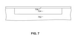
- FIGS. 7 through 17illustrate a method for manufacturing a scissor style magnetic sensor having a magnetic bias structure according to an embodiment of the invention.
- a substrate 702is provided, which can be a layer of a non-magnetic, electrically insulating material such as alumina.
- An electrically conductive, magnetic shield 704constructed of a material such as NiFe is formed on or into the substrate 702 .
- the shield 704is preferably constructed such that the shield is embedded into the substrate 702 and has an upper surface that is coplanar with the surface of the substrate. 702 .
- a series of sensor layers 706is deposited over the magnetic shield 704 and the substrate 702 .
- the series of sensor layerscan include layers of the sensor stack 302 described above with reference to FIG. 3 , but also includes layers of sensors having various other structures as well.
- the series of sensor layers 706preferably includes a layer of material that is resistant to chemical mechanical polishing (CMP resistant material) such as diamond like carbon (DLC) or amorphous carbon a its top.
- CMP resistant materialsuch as diamond like carbon (DLC) or amorphous carbon a its top.
- a mask structure 802is formed.
- This mask structurecan include various layers. These various mask layers can include, for example, a bottom hard mask layer 804 preferably constructed of a material that is resistant to chemical mechanical polishing, an image transfer layer, such as DURIMIDE® 806 , an optional top hard mask/bottom antireflective coating layer 808 , and a photoresist layer 810 .
- the photoresist layer 810can be patterned as desired by a photolithographic patterning and developing process, and the pattern of this image transfer layer can be transferred onto the underlying layers 804 , 806 , 808 by one or more reactive ion etching processes and/or ion milling.
- the patterned mask 802has a central covered portion 804 (which will define a sensor area and first and second openings at either end of the central portion.
- the dashed line denoted (ABS)indicates the location of the air bearing surface plane. Therefore, the openings in the mask are in front of and behind the sensor area.
- FIG. 9shows a top down view of the mask 802 and openings through which the sensor layers 706 are exposed.
- an ion milling processis performed to remove portions of the sensor layers 706 that are not protected by the mask (e.g. parts that are exposed through the openings in the mask 802 ), leaving a structure as shown in FIG. 10 .
- a thin insulation layer 1102is deposited followed by a layer of magnetic material having a high coercivity, (hard magnetic material) 1104 .
- the insulation layercan be SiN and is preferably deposited by a conformal deposition process such as ion beam deposition to a thickness of about 30 Angstroms.
- the hard magnetic material 1104can be constructed of a material such as CoPt or CoPtCr and is preferably deposited to at thickness that is about as high as the height of the sensor layers 706 .
- the hard bias layer 1104is preferably deposited to a thickness that is about 4 times the thickness of the insulation layer or about 120 Angstroms.
- CMP resistant materialsuch as diamond like carbon
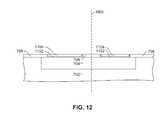
- a wrinkle bake processis then performed, followed by a chemical liftoff process to remove the mask 802 .
- Thisis followed by a chemical mechanical polishing process, which is then followed by a reactive ion etching to remove the CMP resistant material.
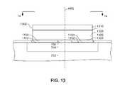
- the mask 1302can include a CMP resistant hard mask 1304 such as DLC, an image transfer layer 1306 such as DURIMIDE®, an optional top hard mask/bottom antireflective coating layer 1308 and a photoresist mask 1310 .
- the photoresist mask 1310is photolithographically patterned to the desired mask shape, and the shape of the photoresist mask 1310 can be transferred onto the underlying layers 1304 , 1306 , 1308 by one or more reactive ion etching processes.
- the pattern of the mask 1302can be better seen with reference to FIG. 14 which shows a top down view.
- the mask 1302has a narrow, constant width, throat portion 1402 that extends over the portion of the sensor material layer 506 that is between the two portions of hard bias material 1104 .
- the throat portion 1402also extends slightly over the hard bias material 1104 as well.
- This throat portion 1402has a width that defines the width of the sensor 302 and that also defines the neck portion 504 of the hard bias structure 402 (as described above with reference to FIG. 5 ).
- the mask 1302also has a flared portion 1404 that is formed over the hard bias material 1104 . This flared portion will define the wedged or tapered portion of the hard bias layer structure as will be seen.
- a second ion millingcan be performed to remove sensor material 706 and hard bias material 1302 that is not protected by the mask 1302 .
- a fill layeris deposited. Most preferably, this includes depositing an anti-diffusion layer such as 30 Angstroms of SiN 1502 , followed by a non-magnetic, dielectric fill layer such as alumina 1504 followed by a CMP resistant layer such as about 2 Angstroms of diamond like carbon (DLC).
- an anti-diffusion layersuch as 30 Angstroms of SiN 1502
- a non-magnetic, dielectric fill layersuch as alumina 1504
- a CMP resistant layersuch as about 2 Angstroms of diamond like carbon (DLC).
- FIG. 17shows a top down view of the structure of FIG. 16 .
- a dicing and lapping operationcan be performed to define the air bearing surface. The lapping operation removes material from the direction indicated by arrows 1702 and is terminated when the air bearing surface plan (dashed line ABS) has been reached.
Landscapes
- Physics & Mathematics (AREA)
- Condensed Matter Physics & Semiconductors (AREA)
- General Physics & Mathematics (AREA)
- Magnetic Heads (AREA)
- Hall/Mr Elements (AREA)
- Measuring Magnetic Variables (AREA)
Abstract
Description
- The present invention relates to magnetic data recording and more particularly to an improved magnetic hard bias structure for use with a scissor type magnetoresistive sensor.
- The heart of a computer is an assembly that is referred to as a magnetic disk drive. The magnetic disk drive includes a rotating magnetic disk, write and read heads that are suspended by a suspension arm adjacent to a surface of the rotating magnetic disk and an actuator that swings the suspension arm to place the read and write heads over selected circular tracks on the rotating disk. The read and write heads are directly located on a slider that has an air bearing surface (ABS). The suspension arm biases the slider into contact with the surface of the disk when the disk is not rotating, but when the disk rotates air is swirled by the rotating disk. When the slider rides on the air bearing, the write and read heads are employed for writing magnetic impressions to and reading magnetic impressions from the rotating disk. The read and write heads are connected to processing circuitry that operates according to a computer program to implement the writing and reading functions.
- The write head includes at least one coil, a write pole and one or more return poles. Whet a current flows through the coil, a resulting magnetic field causes a magnetic flux to flow through the write pole, which results in a magnetic write field emitting from the tip of the write pole. This magnetic field is sufficiently strong that it locally magnetizes a portion of the adjacent magnetic disk, thereby recording a bit of data. The write field, then, travels through a magnetically soft under-layer of the magnetic medium to return to the return pole of the write head.
- A magnetoresistive sensor such as a Giant Magnetoresistive (GMR) sensor, or a Tunnel Junction Magnetoresisive (TMR) sensor can be employed to read a magnetic signal from the magnetic media. The sensor includes a nonmagnetic conductive layer (if the sensor is a GMR sensor) or a thin nonmagnetic, electrically insulating barrier layer (if the sensor is a TMR sensor) sandwiched between first and second ferromagnetic layers, hereinafter referred to as a pinned layer and a free layer. Magnetic shields are positioned above and below the sensor stack and can also serve as first and second electrical leads so that the electrical current travels perpendicularly to the plane of the free layer, spacer layer and pinned layer (current perpendicular to the plane (CPP) mode of operation). The magnetization direction of the pinned layer is pinned perpendicular to the air bearing surface (ABS) and the magnetization direction of the free layer is located parallel to the ABS, but free to rotate in response to external magnetic fields. The magnetization of the pinned layer is typically pinned by exchange coupling with an antiferromagnetic layer.
- When the magnetizations of the pinned and free layers are parallel with respect to one another, scattering of the conduction electrons is minimized and when the magnetizations of the pinned and free layer are antiparallel, scattering is maximized. In a read mode the resistance of the spin valve sensor changes about linearly with the magnitudes of the magnetic fields from the rotating disk. When a sense current is conducted through the spin valve sensor, resistance changes cause potential changes that are detected and processed as playback signals.
- With the need to ever increase data density various novel sensor structures have been investigated. One way to increase data density is to reduce the sensor gap thickness which defines the bit length. Standard GMR or TMR sensors use an antiferromagnetic layer to pin the pinned layer structure of the sensor. In order to function as an antiferromagnetic layer, these layers must be very thick relative to the other sensor layers. This of course increases the gap thickness, which increases the bit length, which decreases data density.
- A sensor that has been investigated to overcome this challenge is a sensor that is known as a scissor sensor. Such a sensor has two free magnetic layers with magnetizations that move in a scissor fashion relative to each other. Such a sensor shows promise because it does not require a thick antiferromagnetic layer. However, such a sensor presents challenges with regard to magnetic biasing of the two free layers. Therefore, there remains a need for a sensor that can reduce gap thickness such as by eliminating an AFM layer, while providing robust, reliable and workable biasing of the magnetic layers.
- The present invention provides a magnetic sensor comprising, a sensor stack including first and second magnetic layers and a non magnetic layer sandwiched between the first and second magnetic layers, the sensor stack having a front edge located at an air bearing surface a back edge located opposite the front edge and first and second laterally opposed sides each extending from the front edge to the back edge. The sensor also includes a magnetic bias structure located adjacent to the back edge of the sensor stack for providing a magnetic bias field to the sensor stack, the magnetic bias structure including a neck portion near the sensor stack that has first and second sides that are aligned with the first and second sides of the sensor stack and having a flared portion.
- The magnetic sensor can be constructed by a method that includes forming a magnetic shield and depositing a series of sensor layers over the magnetic shield. A first mask is formed over the series of sensor layers, the first mask being configured to define front and back edges of a sensor structure. A first ion milling is performed to remove portions of the series of sensor layers that are not protected by the first mask, thereby defining front and back edge of the sensor structure. A magnetic hard bias material is deposited, and the first mask is removed. A second mask is then formed, the second mask including a portion configured to define a sensor width and having another portion configured to define a shape of a magnetic hard bias structure extending from the back edge of the sensor. A second ion milling is performed to remove portions of the sensor material and magnetic hard bias material that are not protected by the second mask.
- The novel hard bias structure having a neck portion that is aligned with the first and second sides of the sensor stack and having a tapered or wedged portion extending backwards from the neck portion provides a strong robust magnetic bias field for biasing the magnetic layers of the sensor stack. This bias field can be optimized by forming the tapered or wedged portion with side edges that define an angle of 25-50 degrees with respect to the air bearing surface.
- These and other features and advantages of the invention will be apparent upon reading of the following detailed description of preferred embodiments taken in conjunction with the Figures in which like reference numerals indicate like elements throughout.
- For a fuller understanding of the nature and advantages of this invention, as well as the preferred mode of use, reference should be made to the following detailed description read in conjunction with the accompanying drawings which are not to scale.
FIG. 1 is a schematic illustration of a disk drive system in which the invention might be embodied;FIG. 2 is an ABS view of a slider illustrating the location of a magnetic head thereon;FIG. 3 is an enlarged ABS view of a magnetoresistive sensor according to an embodiment of the invention;FIG. 4 is an exploded, top-down, schematic view of layers of the magnetoresistive sensor ofFIG. 3 ;FIG. 5 is a top down view of a magnetoresistive sensor and magnetic bias structure;FIG. 6 is a table illustrating bias fields for various hard bias structure configurations;FIGS. 7-17 are views of a magnetic sensor in various intermediate stages of manufacture, illustrating a method for manufacturing a magnetic sensor and hard bias structure according to an embodiment of the invention; andFIG. 18 is a top down view of a top down view of a magnetoresistive sensor and hard bias structure according to an alternate embodiment of the invention.- The following description is of the best embodiments presently contemplated for carrying out this invention. This description is made for the purpose of illustrating the general principles of this invention and is not meant to limit the inventive concepts claimed herein.
- Referring now to
FIG. 1 , there is shown adisk drive 100 embodying this invention. As shown inFIG. 1 , at least one rotatablemagnetic disk 112 is supported on aspindle 114 and rotated by adisk drive motor 118. The magnetic recording on each disk is in the form of annular patterns of concentric data tracks (not shown) on themagnetic disk 112. - At least one
slider 113 is positioned near themagnetic disk 112, eachslider 113 supporting one or moremagnetic head assemblies 121. As the magnetic disk rotates,slider 113 moves radially in and out over thedisk surface 122 so that themagnetic head assembly 121 can access different tracks of the magnetic disk where desired data are written. Eachslider 113 is attached to anactuator arm 119 by way of asuspension 115. Thesuspension 115 provides a slight spring force whichbiases slider 113 against thedisk surface 122. Eachactuator arm 119 is attached to an actuator means127. The actuator means127 as shown inFIG. 1 may be a voice cod motor (VCM). The VCM comprises a coil movable within a fixed magnetic field, the direction and speed of the coil movements being controlled by the motor current signals supplied bycontroller 129. - During operation of the disk storage system, the rotation of the
magnetic disk 112 generates an air bearing between theslider 113 and thedisk surface 122 which exerts an upward force or lift on the slider. The air bearing thus counter-balances the slight spring force ofsuspension 115 and supportsslider 113 off and slightly above the disk surface by a small, substantially constant spacing during normal operation. - The various components of the disk storage system are controlled in operation by control signals generated by
control unit 129, such as access control signals and internal dock signals. Typically, thecontrol unit 129 comprises logic control circuits, storage means and a microprocessor. Thecontrol unit 129 generates control signals to control various system operations such as drive motor control signals online 123 and head position and seek control signals online 128. The control signals online 128 provide the desired current profiles to optimally move andposition slider 113 to the desired data track ondisk 112. Write and read signals are communicated to and from write and readheads 121 by way ofrecording channel 125. - With reference to
FIG. 2 , the orientation of themagnetic head 121 in aslider 113 can be seen in more detail.FIG. 2 is an ABS view of theslider 113, and as can be seen the magnetic head including an inductive write head and a read sensor, is located at a trailing edge of the slider. The above description of a typical magnetic disk storage system and the accompanying illustration ofFIG. 1 are for representation purposes only. It should be apparent that disk storage systems may contain a large number of disks and actuators, and each actuator may support a number of sliders. FIG. 3 shows an air bearing surface (ABS) view of amagnetic sensor 300 according to an embodiment of the invention. Thesensor 300 includes asensor stack 302 that is sandwiched between first and secondmagnetic shields sensor stack 302 as well as functioning as magnetic shields.- The
sensor stack 302 includes first and secondmagnetic layers non-magnetic layer 312 sandwiched between themagnetic layers sensor 300 is preferably a tunnel junction sensor, wherein thelayer 312 is a non-magnetic, electrically insulating layer such as MgO. However, thesensor 300 could also be a giant magnetoresistive sensor (GMR sensor), in which case thelayer 312 would be a non-magnetic, electrically conductive layer such as Cu, Ag, AgSn. Thesensor stack 302 can also include aseed layer 314, provided at the bottom of thesensor stack 300 to initiate a desired grain formation in the above formed layers. Thesensor stack 300 can also include acapping lay 316 such as Ru/Ta/Ru or Ru to protect the under-lying sensor layers during manufacture. The space to either side of thesensor stack 302, between themagnetic shields material - The
magnetic layers magnetizations magnetizations FIG. 4 shows a top down, exploded, schematic view of themagnetic layers magnetizations magnetization 322 is shown in dashed line to indicate that it is the magnetization of thelayer 308, which is hidden behind themagnetic layer 310. Amagnetic bias structure 402 located behind the air bearing surface (ABS), which applies a magnetic bias field that pulls themagnetizations magnetizations relative orientations magnetic layers FIG. 3 ) based on the spin dependent tunneling effect of electrons passing through thethin barrier layer 312.- Because the relative movement of the
magnetizations bias layer 402 must be sufficiently strong to overcome the magnetic anisotropy of themagnetic layers magnetizations magnetizations hard bias structure 402 that provides robust biasing. FIG. 5 shows an expanded view of asensor stack 302 andhard bias structure 402 according to an embodiment of the invention. Areas outside of thesensor stack 302 and hard bias structure can be filled with a non-magnetic, electrically insulating material such as alumina and may include the fill layers318,320 described above with reference toFIG. 3 . Also, thesensor 302 is separated from thehard bias structure 402 by a thin, non-magnetic, electrically insulatinglayer 505, which can be a material such as alumina and which preferably also covers thebottom shield 304 in order to prevent shunting of sense current through thehard bias layer 402.- As can be seen, the hard bias structure includes a
neck portion 504 that hassides second sides sensor stack 302. Thehard bias structure 402 also includes a flared portion having flaredsides sides neck portion 504, provide and an optimal magnetic bias field for use with a scissor type sensor. - The benefit of the above described
hard bias structure 402 can be better understood with reference toFIG. 6 which shows the hard bias field for various hard bias layer shapes. For purposes of the table ofFIG. 6 , the hard bias field (HBF) is the field as measured at the center of the sensor302 (FIG. 5 ). In the table ofFIG. 6 , a basic hard bias structure that extends straight back from the sensor is shown in column I and is used as a reference for the other hard bias shapes. Because this is the reference shape, the HBF for this structure in column I is denoted as being zero for purposes of comparison with the other shapes. Column II shows that a bias structure that is significantly wider than the sensor, but extends straight outward from the sensor has a50% increase in bias field compared with the structure of column I. Column III shows that the bias field for a bias structure having a wedge shape (i.e. shallow tapered front edge) with the taper initiating right at the back edge of the sensor (e.g. no neck portion) provides an 84% increase in bias field. Column IV shows a structure similar to that of column III, but with a sharper taper, and shows that this structure provides a 99% increase in bias field. In column III, the taper angle is 25-50 degrees relative to a plane that is parallel with the air bearing surface. Column V shows a bias structure having a shallow taper and also having a neck portion at the back edge of the sensor. As can be seen, this structure provides a 109% increase in bias field. Finally, column VI shows the bias field from a bias structure that has both a neck and a steep tapered wedge (forming an angle of 25-50 degrees relative to the air bearing surface). This structure provides a bias field that has a 117% increase compared with the structure of column I. As can be seen, this structure of column VI provides the highest bias field of all of the structures shown inFIG. 6 . FIG. 18 shows a top down view of amagnetoresistive sensor 302 having a hard bias structure1800 according Lo an alternate embodiment of the invention. Like the embodiment described above with regard toFIG. 5 , the hard bias structure1800 extends from the back edge of thesensor 302 and is separated from the sensor by athin insulation layer 505. The hard bias structure includes aneck portion 504. The bias structure also includes a flared portion having a front edge portion1702 (nearest to the neck504) that defines an angle θ of 25-50 degrees with respect to the ABS. The hard bias structure1800 also includes a secondtapered edge portion 1704 that is further from theneck portion 504 than thefirst edge portion 1702, theedge 1704 defining an angle with respect to the ABS that is greater than θ, but which is less than 90 degrees.FIGS. 7 through 17 , illustrate a method for manufacturing a scissor style magnetic sensor having a magnetic bias structure according to an embodiment of the invention. With particular reference toFIG. 7 , asubstrate 702 is provided, which can be a layer of a non-magnetic, electrically insulating material such as alumina. An electrically conductive,magnetic shield 704, constructed of a material such as NiFe is formed on or into thesubstrate 702. Theshield 704 is preferably constructed such that the shield is embedded into thesubstrate 702 and has an upper surface that is coplanar with the surface of the substrate.702. A series of sensor layers706 is deposited over themagnetic shield 704 and thesubstrate 702. The series of sensor layers can include layers of thesensor stack 302 described above with reference toFIG. 3 , but also includes layers of sensors having various other structures as well. The series ofsensor layers 706 preferably includes a layer of material that is resistant to chemical mechanical polishing (CMP resistant material) such as diamond like carbon (DLC) or amorphous carbon a its top.- Then, with reference to
FIG. 8 , amask structure 802 is formed. This mask structure can include various layers. These various mask layers can include, for example, a bottomhard mask layer 804 preferably constructed of a material that is resistant to chemical mechanical polishing, an image transfer layer, such asDURIMIDE® 806, an optional top hard mask/bottomantireflective coating layer 808, and aphotoresist layer 810. Thephotoresist layer 810 can be patterned as desired by a photolithographic patterning and developing process, and the pattern of this image transfer layer can be transferred onto theunderlying layers mask 802 has a central covered portion804 (which will define a sensor area and first and second openings at either end of the central portion. The dashed line denoted (ABS) indicates the location of the air bearing surface plane. Therefore, the openings in the mask are in front of and behind the sensor area. The pattern of themask 802 can be better understood with reference toFIG. 9 which shows a top down view of themask 802 and openings through which the sensor layers706 are exposed. - With the mask thus formed, an ion milling process is performed to remove portions of the sensor layers706 that are not protected by the mask (e.g. parts that are exposed through the openings in the mask802), leaving a structure as shown in
FIG. 10 . Then, as show inFIG. 11 , athin insulation layer 1102 is deposited followed by a layer of magnetic material having a high coercivity, (hard magnetic material)1104. The insulation layer can be SiN and is preferably deposited by a conformal deposition process such as ion beam deposition to a thickness of about 30 Angstroms. The hardmagnetic material 1104 can be constructed of a material such as CoPt or CoPtCr and is preferably deposited to at thickness that is about as high as the height of the sensor layers706. Thehard bias layer 1104 is preferably deposited to a thickness that is about 4 times the thickness of the insulation layer or about 120 Angstroms. - Then, another layer of material that is resistant to chemical mechanical polishing (CMP resistant material) such as diamond like carbon (not shown) is deposited. A wrinkle bake process is then performed, followed by a chemical liftoff process to remove the
mask 802. This is followed by a chemical mechanical polishing process, which is then followed by a reactive ion etching to remove the CMP resistant material. These processes leave a planarized structure as shown inFIG. 12 , having a smooth planar surface1202 across the hard bias layers1104 and thesensor material 706. - With reference now to
FIG. 13 , anothermask structure 1302 is formed. Like the previously formedmask 802, themask 1302 can include a CMP resistanthard mask 1304 such as DLC, animage transfer layer 1306 such as DURIMIDE®, an optional top hard mask/bottomantireflective coating layer 1308 and aphotoresist mask 1310. Thephotoresist mask 1310 is photolithographically patterned to the desired mask shape, and the shape of thephotoresist mask 1310 can be transferred onto theunderlying layers - The pattern of the
mask 1302 can be better seen with reference toFIG. 14 which shows a top down view. As can be seen, themask 1302 has a narrow, constant width,throat portion 1402 that extends over the portion of thesensor material layer 506 that is between the two portions ofhard bias material 1104. Preferably, however, thethroat portion 1402 also extends slightly over thehard bias material 1104 as well. Thisthroat portion 1402 has a width that defines the width of thesensor 302 and that also defines theneck portion 504 of the hard bias structure402 (as described above with reference toFIG. 5 ). Themask 1302 also has a flared portion1404 that is formed over thehard bias material 1104. This flared portion will define the wedged or tapered portion of the hard bias layer structure as will be seen. - With the
second mask 1302 in place, a second ion milling can be performed to removesensor material 706 andhard bias material 1302 that is not protected by themask 1302. Then, with reference toFIG. 15 , a fill layer is deposited. Most preferably, this includes depositing an anti-diffusion layer such as 30 Angstroms ofSiN 1502, followed by a non-magnetic, dielectric fill layer such asalumina 1504 followed by a CMP resistant layer such as about 2 Angstroms of diamond like carbon (DLC). - This can then be followed by a wrinkle bake process and a chemical liftoff process to remove all or a portion of the
mask 1302, followed by a chemical mechanical polishing process to remove any remaining mask materials and to polarize the structure. A reactive ion etching RIE can then be performed to remove any of the remaining CMPresistant material FIG. 16 , with all of themask 1302 and CMP resistant material removed and with a smooth planar surface across thesensor material 706hard bias 1104 and filllayer 1504. - A magnetic material can then be electroplated over this structure to form an upper shield (not shown in
FIG. 16 , but shown asshield 306 inFIG. 3 .FIG. 17 shows a top down view of the structure ofFIG. 16 . After the sensor and any other necessary structures have been formed (such as a write head, not shown), a dicing and lapping operation can be performed to define the air bearing surface. The lapping operation removes material from the direction indicated byarrows 1702 and is terminated when the air bearing surface plan (dashed line ABS) has been reached. - While various embodiments have been described above, it should be understood that they have been presented by way of example only and not limitation. Other embodiments falling within the scope of the invention may also become apparent to those skilled in the art. Thus, the breadth and scope of the invention should not be limited by any of the above-described exemplary embodiments, but should be defined only in accordance with the following claims and their equivalents.
Claims (21)
Priority Applications (2)
| Application Number | Priority Date | Filing Date | Title |
|---|---|---|---|
| US13/251,100US8907666B2 (en) | 2011-09-30 | 2011-09-30 | Magnetic bias structure for magnetoresistive sensor having a scissor structure |
| JP2012215495AJP5914283B2 (en) | 2011-09-30 | 2012-09-28 | Magnetic bias structure of magnetoresistive sensor with scissors structure |
Applications Claiming Priority (1)
| Application Number | Priority Date | Filing Date | Title |
|---|---|---|---|
| US13/251,100US8907666B2 (en) | 2011-09-30 | 2011-09-30 | Magnetic bias structure for magnetoresistive sensor having a scissor structure |
Publications (2)
| Publication Number | Publication Date |
|---|---|
| US20130082696A1true US20130082696A1 (en) | 2013-04-04 |
| US8907666B2 US8907666B2 (en) | 2014-12-09 |
Family
ID=47991959
Family Applications (1)
| Application Number | Title | Priority Date | Filing Date |
|---|---|---|---|
| US13/251,100Active2032-10-24US8907666B2 (en) | 2011-09-30 | 2011-09-30 | Magnetic bias structure for magnetoresistive sensor having a scissor structure |
Country Status (2)
| Country | Link |
|---|---|
| US (1) | US8907666B2 (en) |
| JP (1) | JP5914283B2 (en) |
Cited By (14)
| Publication number | Priority date | Publication date | Assignee | Title |
|---|---|---|---|---|
| US8675318B1 (en) | 2011-11-22 | 2014-03-18 | Western Digital (Fremont), Llc | Method and system for providing a read transducer having a reduced shield-to-shield spacing |
| US8711528B1 (en) | 2012-06-29 | 2014-04-29 | Western Digital (Fremont), Llc | Tunnel magnetoresistance read head with narrow shield-to-shield spacing |
| US8760822B1 (en) | 2012-11-28 | 2014-06-24 | Western Digital (Fremont), Llc | Method and system for providing a read transducer having an extended pinned layer and soft magnetic bias structures with improved stability |
| US9147404B1 (en) | 2015-03-31 | 2015-09-29 | Western Digital (Fremont), Llc | Method and system for providing a read transducer having a dual free layer |
| US9153258B2 (en) | 2013-12-03 | 2015-10-06 | HGST Netherlands B.V. | Scissor magnetic read sensor with novel multi-layer bias structure for uniform free layer biasing |
| US9214172B2 (en) | 2013-10-23 | 2015-12-15 | Western Digital (Fremont), Llc | Method of manufacturing a magnetic read head |
| US9269382B1 (en) | 2012-06-29 | 2016-02-23 | Western Digital (Fremont), Llc | Method and system for providing a read transducer having improved pinning of the pinned layer at higher recording densities |
| US9318130B1 (en) | 2013-07-02 | 2016-04-19 | Western Digital (Fremont), Llc | Method to fabricate tunneling magnetic recording heads with extended pinned layer |
| US9378761B1 (en) | 2015-04-22 | 2016-06-28 | HGST Netherlands B.V. | System for adjusting bias of relative magnetizations of ferromagnetic layers in a magnetoresistive sensor |
| US9406320B2 (en) | 2014-08-20 | 2016-08-02 | HGST Netherlands B.V. | Scissor unidirectional biasing with hard bias stabilized soft bias |
| CN109298455A (en)* | 2018-07-31 | 2019-02-01 | 中国地质大学(武汉) | Three-axis TMR magnetometer applied to UAV aerial magnetic survey platform |
| US20190279804A1 (en)* | 2018-03-06 | 2019-09-12 | Allegro Microsystems, Llc | Magnetoresistance Element With Extended Linear Response to Magnetic Fields |
| CN113884774A (en)* | 2021-08-30 | 2022-01-04 | 西安工程大学 | A device and method for continuously testing the performance of electromagnetic shielding clothing reflecting electromagnetic waves |
| US12359904B2 (en) | 2023-01-26 | 2025-07-15 | Allegro Microsystems, Llc | Method of manufacturing angle sensors including magnetoresistance elements including different types of antiferromagnetic materials |
Families Citing this family (3)
| Publication number | Priority date | Publication date | Assignee | Title |
|---|---|---|---|---|
| US20150002961A1 (en)* | 2013-06-26 | 2015-01-01 | HGST Netherlands B.V. | Scissor magnetic sensor having a back edge soft magnetic bias structure |
| US9513349B2 (en)* | 2014-02-06 | 2016-12-06 | HGST Netherlands B.V. | Scissor type magnetic sensor with high magnetic moment bias structure for reduced signal asymmetry |
| US9940955B2 (en) | 2015-12-01 | 2018-04-10 | Western Digital Technologies, Inc. | Tunnel magnetoresistance magnetic sensor with scissor sensor and multi-seed layer configuration |
Citations (11)
| Publication number | Priority date | Publication date | Assignee | Title |
|---|---|---|---|---|
| US5714679A (en)* | 1996-10-02 | 1998-02-03 | Nichols; Steven J. | Portable apparatus for testing an internal combustion engine |
| US6310590B1 (en)* | 1986-01-15 | 2001-10-30 | Texas Digital Systems, Inc. | Method for continuously controlling color of display device |
| US7034517B2 (en)* | 2004-03-15 | 2006-04-25 | Fluke Corporation | Multimeter with filtered measurement mode |
| US20060209471A1 (en)* | 2005-03-17 | 2006-09-21 | Fujitsu Limited | Magnetoresistive element and method of manufacturing the same |
| US20090073616A1 (en)* | 2007-09-17 | 2009-03-19 | Tdk Corporation | Magneto-resistive effect device of the cpp structure and magnetic disk system |
| US20090109580A1 (en)* | 2007-10-26 | 2009-04-30 | Ayukawa Toshiyuki | Magnetic field detecting element including tri-layer stack with stepped portion |
| US20090213502A1 (en)* | 2008-02-25 | 2009-08-27 | Daisuke Miyauchi | Magneto-resistance effect element having stack with dual free layer and a plurality of bias magnetic layers |
| US20100232074A1 (en)* | 2009-03-13 | 2010-09-16 | Tdk Corporation | Magnetoresistive effect element and magnetic disk device |
| US20110007426A1 (en)* | 2009-07-13 | 2011-01-13 | Seagate Technology Llc | Trapezoidal back bias and trilayer reader geometry to enhance device performance |
| US8208230B2 (en)* | 2008-04-10 | 2012-06-26 | Headway Technologies, Inc. | Binary output reader structure (BORS) with high utilization rate |
| US8599520B1 (en)* | 2011-12-20 | 2013-12-03 | Western Digital (Fremont), Llc | Method and system for providing a read transducer having an adaptive read sensor track width |
Family Cites Families (30)
| Publication number | Priority date | Publication date | Assignee | Title |
|---|---|---|---|---|
| US5452163A (en)* | 1993-12-23 | 1995-09-19 | International Business Machines Corporation | Multilayer magnetoresistive sensor |
| US5576914A (en) | 1994-11-14 | 1996-11-19 | Read-Rite Corporation | Compact read/write head having biased GMR element |
| EP0768642A3 (en) | 1995-10-13 | 1998-12-16 | Read-Rite Corporation | Magnetic head with biased GMR element and sense current compensation |
| US5818685A (en) | 1997-05-05 | 1998-10-06 | Read-Rite Corporation | CIP GMR sensor coupled to biasing magnet with spacer therebetween |
| US6005753A (en) | 1998-05-29 | 1999-12-21 | International Business Machines Corporation | Magnetic tunnel junction magnetoresistive read head with longitudinal and transverse bias |
| JP2001351208A (en) | 2000-06-12 | 2001-12-21 | Mitsumi Electric Co Ltd | Magnetoresistive magnetic head |
| CN1459094A (en) | 2000-09-19 | 2003-11-26 | 西加特技术有限责任公司 | Giant magnetoresistire sensor having self-consistent demagnetization fields |
| US6724583B2 (en) | 2000-12-19 | 2004-04-20 | Seagate Technology Llc | Adjustable permanent magnet bias |
| US6847509B2 (en) | 2001-02-01 | 2005-01-25 | Kabushiki Kaisha Toshiba | Magnetoresistive head and perpendicular magnetic recording-reproducing apparatus |
| US6667862B2 (en) | 2001-02-20 | 2003-12-23 | Carnegie Mellon University | Magnetoresistive read head having permanent magnet on top of magnetoresistive element |
| US7035062B1 (en) | 2001-11-29 | 2006-04-25 | Seagate Technology Llc | Structure to achieve sensitivity and linear density in tunneling GMR heads using orthogonal magnetic alignments |
| US7719802B2 (en) | 2003-09-23 | 2010-05-18 | Seagate Technology Llc | Magnetic sensor with electrically defined active area dimensions |
| JP2005109241A (en) | 2003-09-30 | 2005-04-21 | Tdk Corp | Magnetoresistance effect element, manufacturing method thereof, and magnetic head |
| US7177122B2 (en) | 2003-10-27 | 2007-02-13 | Seagate Technology Llc | Biasing for tri-layer magnetoresistive sensors |
| US20070030603A1 (en) | 2004-04-02 | 2007-02-08 | Isamu Sato | Stabilizer for magnetoresistive head in current perpendicular to plane mode and method of manufacture |
| JP4002909B2 (en) | 2004-06-04 | 2007-11-07 | アルプス電気株式会社 | CPP type giant magnetoresistive head |
| JP4308109B2 (en) | 2004-09-07 | 2009-08-05 | Tdk株式会社 | Magnetoresistive element, thin film magnetic head, head gimbal assembly, and hard disk drive |
| JP2007250061A (en) | 2006-03-15 | 2007-09-27 | Fujitsu Ltd | Magnetic sensor and magnetic disk device |
| US7813086B2 (en) | 2007-05-21 | 2010-10-12 | Tdk Corporation | Thin film magnetic head comprising metal layer and having improved asymmetry characteristic and method of producing the same |
| US7869165B2 (en) | 2007-07-30 | 2011-01-11 | Tdk Corporation | Magnetic field detecting element having stack with a plurality of free layers and side shield layers |
| US7843668B2 (en) | 2007-12-27 | 2010-11-30 | Tdk Corporation | Magnetoresistive element including two ferromagnetic layers |
| US7876534B2 (en) | 2008-01-15 | 2011-01-25 | Tdk Corporation | Magneto-resistive effect device of the CPP type, and magnetic disk system |
| US7881021B2 (en) | 2008-01-30 | 2011-02-01 | Tdk Corporation | CPP type magnetoresistive device with biasing arrangement for ferromagnetic layers having respective magnetizations orthogonal to one another, and magnetic disk system using same |
| US8098464B2 (en) | 2008-02-19 | 2012-01-17 | Tdk Corporation | CPP-type magneto resistance element having a pair of free layers and spacer layer sandwiched therebetween |
| US8189303B2 (en) | 2008-08-12 | 2012-05-29 | Tdk Corporation | Thin film magnetic head having a pair of magnetic layers whose magnetization is controlled by shield layers |
| US8023230B2 (en) | 2008-10-27 | 2011-09-20 | Tdk Corporation | Magnetoresistive element including a pair of ferromagnetic layers coupled to a pair of shield layers |
| JP2010134997A (en) | 2008-12-04 | 2010-06-17 | Hitachi Global Storage Technologies Netherlands Bv | Magnetoresistive head having cpp structure |
| US8147994B2 (en)* | 2009-02-26 | 2012-04-03 | Tdk Corporation | Layered structure having FePt system magnetic layer and magnetoresistive effect element using the same |
| US8179642B2 (en) | 2009-09-22 | 2012-05-15 | Tdk Corporation | Magnetoresistive effect element in CPP structure and magnetic disk device |
| US20130083432A1 (en) | 2011-09-29 | 2013-04-04 | Hitachi Global Storage Technologies Netherlands B.V. | Magnetic bias structure for magnetoresistive sensor |
- 2011
- 2011-09-30USUS13/251,100patent/US8907666B2/enactiveActive
- 2012
- 2012-09-28JPJP2012215495Apatent/JP5914283B2/enactiveActive
Patent Citations (11)
| Publication number | Priority date | Publication date | Assignee | Title |
|---|---|---|---|---|
| US6310590B1 (en)* | 1986-01-15 | 2001-10-30 | Texas Digital Systems, Inc. | Method for continuously controlling color of display device |
| US5714679A (en)* | 1996-10-02 | 1998-02-03 | Nichols; Steven J. | Portable apparatus for testing an internal combustion engine |
| US7034517B2 (en)* | 2004-03-15 | 2006-04-25 | Fluke Corporation | Multimeter with filtered measurement mode |
| US20060209471A1 (en)* | 2005-03-17 | 2006-09-21 | Fujitsu Limited | Magnetoresistive element and method of manufacturing the same |
| US20090073616A1 (en)* | 2007-09-17 | 2009-03-19 | Tdk Corporation | Magneto-resistive effect device of the cpp structure and magnetic disk system |
| US20090109580A1 (en)* | 2007-10-26 | 2009-04-30 | Ayukawa Toshiyuki | Magnetic field detecting element including tri-layer stack with stepped portion |
| US20090213502A1 (en)* | 2008-02-25 | 2009-08-27 | Daisuke Miyauchi | Magneto-resistance effect element having stack with dual free layer and a plurality of bias magnetic layers |
| US8208230B2 (en)* | 2008-04-10 | 2012-06-26 | Headway Technologies, Inc. | Binary output reader structure (BORS) with high utilization rate |
| US20100232074A1 (en)* | 2009-03-13 | 2010-09-16 | Tdk Corporation | Magnetoresistive effect element and magnetic disk device |
| US20110007426A1 (en)* | 2009-07-13 | 2011-01-13 | Seagate Technology Llc | Trapezoidal back bias and trilayer reader geometry to enhance device performance |
| US8599520B1 (en)* | 2011-12-20 | 2013-12-03 | Western Digital (Fremont), Llc | Method and system for providing a read transducer having an adaptive read sensor track width |
Cited By (18)
| Publication number | Priority date | Publication date | Assignee | Title |
|---|---|---|---|---|
| US8675318B1 (en) | 2011-11-22 | 2014-03-18 | Western Digital (Fremont), Llc | Method and system for providing a read transducer having a reduced shield-to-shield spacing |
| US9269382B1 (en) | 2012-06-29 | 2016-02-23 | Western Digital (Fremont), Llc | Method and system for providing a read transducer having improved pinning of the pinned layer at higher recording densities |
| US8711528B1 (en) | 2012-06-29 | 2014-04-29 | Western Digital (Fremont), Llc | Tunnel magnetoresistance read head with narrow shield-to-shield spacing |
| US9065043B1 (en) | 2012-06-29 | 2015-06-23 | Western Digital (Fremont), Llc | Tunnel magnetoresistance read head with narrow shield-to-shield spacing |
| US9412400B2 (en) | 2012-06-29 | 2016-08-09 | Western Digital (Fremont), Llc | Tunnel magnetoresistance read head with narrow shield-to-shield spacing |
| US8760822B1 (en) | 2012-11-28 | 2014-06-24 | Western Digital (Fremont), Llc | Method and system for providing a read transducer having an extended pinned layer and soft magnetic bias structures with improved stability |
| US9318130B1 (en) | 2013-07-02 | 2016-04-19 | Western Digital (Fremont), Llc | Method to fabricate tunneling magnetic recording heads with extended pinned layer |
| US9830936B2 (en) | 2013-10-23 | 2017-11-28 | Western Digital (Fremont), Llc | Magnetic read head with antiferromagentic layer |
| US9214172B2 (en) | 2013-10-23 | 2015-12-15 | Western Digital (Fremont), Llc | Method of manufacturing a magnetic read head |
| US9153258B2 (en) | 2013-12-03 | 2015-10-06 | HGST Netherlands B.V. | Scissor magnetic read sensor with novel multi-layer bias structure for uniform free layer biasing |
| US9406320B2 (en) | 2014-08-20 | 2016-08-02 | HGST Netherlands B.V. | Scissor unidirectional biasing with hard bias stabilized soft bias |
| US9147404B1 (en) | 2015-03-31 | 2015-09-29 | Western Digital (Fremont), Llc | Method and system for providing a read transducer having a dual free layer |
| US9378761B1 (en) | 2015-04-22 | 2016-06-28 | HGST Netherlands B.V. | System for adjusting bias of relative magnetizations of ferromagnetic layers in a magnetoresistive sensor |
| US20190279804A1 (en)* | 2018-03-06 | 2019-09-12 | Allegro Microsystems, Llc | Magnetoresistance Element With Extended Linear Response to Magnetic Fields |
| US10840001B2 (en)* | 2018-03-06 | 2020-11-17 | Allegro Microsystems, Llc | Magnetoresistance element with extended linear response to magnetic fields |
| CN109298455A (en)* | 2018-07-31 | 2019-02-01 | 中国地质大学(武汉) | Three-axis TMR magnetometer applied to UAV aerial magnetic survey platform |
| CN113884774A (en)* | 2021-08-30 | 2022-01-04 | 西安工程大学 | A device and method for continuously testing the performance of electromagnetic shielding clothing reflecting electromagnetic waves |
| US12359904B2 (en) | 2023-01-26 | 2025-07-15 | Allegro Microsystems, Llc | Method of manufacturing angle sensors including magnetoresistance elements including different types of antiferromagnetic materials |
Also Published As
| Publication number | Publication date |
|---|---|
| JP2013079954A (en) | 2013-05-02 |
| US8907666B2 (en) | 2014-12-09 |
| JP5914283B2 (en) | 2016-05-11 |
Similar Documents
| Publication | Publication Date | Title |
|---|---|---|
| US8907666B2 (en) | Magnetic bias structure for magnetoresistive sensor having a scissor structure | |
| US8617408B2 (en) | Method for manufacturing a magnetic read sensor with narrow track width using amorphous carbon as a hard mask and localized CMP | |
| US9047894B2 (en) | Magnetic write head having spin torque oscillator that is self aligned with write pole | |
| US9042062B2 (en) | Magnetic sensor with recessed AFM shape enhanced pinning and soft magnetic bias | |
| US7602589B2 (en) | Magnetoresistive sensor having shape enhanced pinning and low lead resistance | |
| US7712206B2 (en) | Method for manufacturing a magnetic write head having a trailing shield with an accurately controlled trailing shield gap thickness | |
| US20120156390A1 (en) | Multi-angle hard bias deposition for optimal hard-bias deposition in a magnetic sensor | |
| US20080151441A1 (en) | Magnetoresistive sensor having an anisotropic hard bias with high coercivity | |
| US8842395B2 (en) | Magnetic sensor having an extended pinned layer and shape enhanced bias structure | |
| US7324310B2 (en) | Self-pinned dual CPP sensor exchange pinned at stripe back-end to avoid amplitude flipping | |
| US8213132B2 (en) | Magnetic sensor having a physically hard insulation layer over a magnetic bias structure | |
| JP5852541B2 (en) | Magnetic bias structure for magnetoresistive sensors | |
| US20120320473A1 (en) | Magnetic sensor having a hard bias seed structure | |
| US7848061B2 (en) | Current perpendicular to plane (CPP) magnetoresistive sensor with back flux guide | |
| US20120187079A1 (en) | Method for manufacturing a magnetic sensor having a flat upper shield | |
| US7788798B2 (en) | Method for manufacturing a perpendicular magnetic write head with wrap around magnetic trailing and side shields | |
| US7446982B2 (en) | Pinning structure with trilayer pinned layer | |
| US8031434B2 (en) | Hybrid, self aligned magnetic write head with a partially plated pole and method of producing same | |
| US20130083432A1 (en) | Magnetic bias structure for magnetoresistive sensor | |
| US9053721B1 (en) | Magnetic read sensor with independently extended pinned layer and seed layer | |
| US8797694B2 (en) | Magnetic sensor having hard bias structure for optimized hard bias field and hard bias coercivity | |
| US9047893B1 (en) | Magnetic sensor having narrow trackwidth and small read gap | |
| US20150118520A1 (en) | Low resistance magnetic sensor with extended pinned layer structure | |
| US20120231296A1 (en) | Method for manufacturing an advanced magnetic read sensor | |
| US8615868B2 (en) | Method for manufacturing a magnetic sensor using two step ion milling |
Legal Events
| Date | Code | Title | Description |
|---|---|---|---|
| AS | Assignment | Owner name:HITACHI GLOBAL STORAGE TECHNOLOGIES NETHERLANDS B. Free format text:ASSIGNMENT OF ASSIGNORS INTEREST;ASSIGNORS:LE, QUANG;LIAO, SIMON H.;WANG, SHUXIA;AND OTHERS;SIGNING DATES FROM 20110926 TO 20110927;REEL/FRAME:027136/0273 | |
| AS | Assignment | Owner name:HGST NETHERLANDS B.V., NETHERLANDS Free format text:CHANGE OF NAME;ASSIGNOR:HITACHI GLOBAL STORAGE TECHNOLOGIES NETHERLANDS B.V.;REEL/FRAME:029341/0777 Effective date:20120723 | |
| FEPP | Fee payment procedure | Free format text:PAYOR NUMBER ASSIGNED (ORIGINAL EVENT CODE: ASPN); ENTITY STATUS OF PATENT OWNER: LARGE ENTITY | |
| STCF | Information on status: patent grant | Free format text:PATENTED CASE | |
| AS | Assignment | Owner name:WESTERN DIGITAL TECHNOLOGIES, INC., CALIFORNIA Free format text:ASSIGNMENT OF ASSIGNORS INTEREST;ASSIGNOR:HGST NETHERLANDS B.V.;REEL/FRAME:040826/0327 Effective date:20160831 | |
| CC | Certificate of correction | ||
| MAFP | Maintenance fee payment | Free format text:PAYMENT OF MAINTENANCE FEE, 4TH YEAR, LARGE ENTITY (ORIGINAL EVENT CODE: M1551) Year of fee payment:4 | |
| AS | Assignment | Owner name:JPMORGAN CHASE BANK, N.A., AS AGENT, ILLINOIS Free format text:SECURITY INTEREST;ASSIGNOR:WESTERN DIGITAL TECHNOLOGIES, INC.;REEL/FRAME:052915/0566 Effective date:20200113 | |
| AS | Assignment | Owner name:WESTERN DIGITAL TECHNOLOGIES, INC., CALIFORNIA Free format text:RELEASE OF SECURITY INTEREST AT REEL 052915 FRAME 0566;ASSIGNOR:JPMORGAN CHASE BANK, N.A.;REEL/FRAME:059127/0001 Effective date:20220203 | |
| MAFP | Maintenance fee payment | Free format text:PAYMENT OF MAINTENANCE FEE, 8TH YEAR, LARGE ENTITY (ORIGINAL EVENT CODE: M1552); ENTITY STATUS OF PATENT OWNER: LARGE ENTITY Year of fee payment:8 | |
| AS | Assignment | Owner name:JPMORGAN CHASE BANK, N.A., ILLINOIS Free format text:PATENT COLLATERAL AGREEMENT - A&R LOAN AGREEMENT;ASSIGNOR:WESTERN DIGITAL TECHNOLOGIES, INC.;REEL/FRAME:064715/0001 Effective date:20230818 Owner name:JPMORGAN CHASE BANK, N.A., ILLINOIS Free format text:PATENT COLLATERAL AGREEMENT - DDTL LOAN AGREEMENT;ASSIGNOR:WESTERN DIGITAL TECHNOLOGIES, INC.;REEL/FRAME:067045/0156 Effective date:20230818 |