US20130005103A1 - Methods for fabricating a finfet integrated circuit on a bulk silicon substrate - Google Patents
Methods for fabricating a finfet integrated circuit on a bulk silicon substrateDownload PDFInfo
- Publication number
- US20130005103A1 US20130005103A1US13/172,635US201113172635AUS2013005103A1US 20130005103 A1US20130005103 A1US 20130005103A1US 201113172635 AUS201113172635 AUS 201113172635AUS 2013005103 A1US2013005103 A1US 2013005103A1
- Authority
- US
- United States
- Prior art keywords
- silicon
- layer
- fin
- overlying
- forming
- Prior art date
- Legal status (The legal status is an assumption and is not a legal conclusion. Google has not performed a legal analysis and makes no representation as to the accuracy of the status listed.)
- Granted
Links
Images


Classifications
- H—ELECTRICITY
- H01—ELECTRIC ELEMENTS
- H01L—SEMICONDUCTOR DEVICES NOT COVERED BY CLASS H10
- H01L21/00—Processes or apparatus adapted for the manufacture or treatment of semiconductor or solid state devices or of parts thereof
- H01L21/02—Manufacture or treatment of semiconductor devices or of parts thereof
- H01L21/04—Manufacture or treatment of semiconductor devices or of parts thereof the devices having potential barriers, e.g. a PN junction, depletion layer or carrier concentration layer
- H01L21/18—Manufacture or treatment of semiconductor devices or of parts thereof the devices having potential barriers, e.g. a PN junction, depletion layer or carrier concentration layer the devices having semiconductor bodies comprising elements of Group IV of the Periodic Table or AIIIBV compounds with or without impurities, e.g. doping materials
- H01L21/30—Treatment of semiconductor bodies using processes or apparatus not provided for in groups H01L21/20 - H01L21/26
- H01L21/302—Treatment of semiconductor bodies using processes or apparatus not provided for in groups H01L21/20 - H01L21/26 to change their surface-physical characteristics or shape, e.g. etching, polishing, cutting
- H01L21/306—Chemical or electrical treatment, e.g. electrolytic etching
- H01L21/3065—Plasma etching; Reactive-ion etching
- H—ELECTRICITY
- H10—SEMICONDUCTOR DEVICES; ELECTRIC SOLID-STATE DEVICES NOT OTHERWISE PROVIDED FOR
- H10D—INORGANIC ELECTRIC SEMICONDUCTOR DEVICES
- H10D30/00—Field-effect transistors [FET]
- H10D30/01—Manufacture or treatment
- H10D30/021—Manufacture or treatment of FETs having insulated gates [IGFET]
- H10D30/024—Manufacture or treatment of FETs having insulated gates [IGFET] of fin field-effect transistors [FinFET]
- H—ELECTRICITY
- H10—SEMICONDUCTOR DEVICES; ELECTRIC SOLID-STATE DEVICES NOT OTHERWISE PROVIDED FOR
- H10D—INORGANIC ELECTRIC SEMICONDUCTOR DEVICES
- H10D30/00—Field-effect transistors [FET]
- H10D30/60—Insulated-gate field-effect transistors [IGFET]
- H10D30/62—Fin field-effect transistors [FinFET]
Definitions
- the present inventiongenerally relates to methods for manufacturing integrated circuits, and more particularly relates to methods for manufacturing FINFET integrated circuits on bulk silicon substrates.
- Transistorssuch as metal oxide semiconductor field effect transistors (MOSFETs) or simply field effect transistors (FETs) or MOS transistors are the core building blocks of the vast majority of semiconductor integrated circuits (ICs).
- a FETincludes source and drain regions between which a current can flow through a channel under the influence of a bias applied to a gate electrode that overlies the channel.
- Some semiconductor ICssuch as high performance microprocessors, can include millions of FETs. For such ICs, decreasing transistor size and thus increasing transistor density has traditionally been a high priority in the semiconductor manufacturing industry. Transistor performance, however, must be maintained even as the transistor size decreases.
- a FINFETis a type of transistor that lends itself to the dual goals of reducing transistor size while maintaining transistor performance.
- the FINFETis a three dimensional transistor formed in a thin fin that extends upwardly from a semiconductor substrate. Transistor performance, often measured by its transconductance, is proportional to the width of the transistor channel. In a FINFET the transistor channel is formed at least along the vertical sidewalls of the fin, so a wide channel, and hence high performance, can be achieved without substantially increasing the area of the substrate surface required by the transistor.
- a methodincludes epitaxially growing a first silicon germanium layer and a second silicon layer overlying a silicon substrate.
- the second silicon layeris etched to form a silicon fin using the first silicon germanium layer as an etch stop.
- the first silicon germanium layer underlying the finis removed to form a void underlying the fin and the void is filled with an insulating material.
- a gate structureis then formed overlying the fin.
- a method for fabricating a FINFET integrated circuitincludes growing a silicon germanium epitaxial layer overlying a silicon substrate and growing a silicon epitaxial layer overlying the silicon germanium epitaxial layer. Shallow trench isolation is formed to define a device region.
- the silicon epitaxial layeris etched in an etchant that etches silicon at a substantially higher etch rate than the etch rate of silicon germanium to form a silicon fin extending across the device region and contacting the shallow trench isolation.
- the silicon germanium epitaxial layeris etched in an etchant that etches silicon germanium at a substantially higher etch rate than the etch rate of silicon to form a void underlying the silicon fin.
- a dielectricis deposited overlying the silicon fin and filling the void, and a planarizing layer is deposited overlying the dielectric.
- the planarizing layer and the dielectricare etched to remove the dielectric overlying the silicon fin and a gate dielectric and a gate electrode are formed overlying the silicon fin.
- a method for fabricating a FINFET integrated circuitincludes forming a shallow trench isolation defining a device region in a silicon substrate.
- a first crystalline layeris formed overlying the substrate and a silicon layer is formed overlying the first crystalline layer.
- the silicon layeris patterned to form a fin extending across the device region and contacting the shallow trench isolation.
- a gate structureis formed overlying the fin.
- the first crystalline layer underlying the finis removed and a dielectric layer is deposited underlying and supporting the fin.
- FIGS. 1-10illustrate methods for fabricating a FINFET IC in accordance with various embodiments.
- FIGS. 1-5 and 7 - 9are cross sectional views
- FIG. 6is a plan view
- FIG. 10is a partially cut away perspective view.
- FIGS. 1-10illustrate method steps for fabricating a FINFET integrated circuit (IC) 100 in accordance with various embodiments.
- the described process steps, procedures, and materialsare to be considered only as exemplary embodiments designed to illustrate to one of ordinary skill in the art methods for practicing the invention; the invention is not to be limited to these exemplary embodiments.
- Various steps in the manufacture of ICsare well known and so, in the interest of brevity, many conventional steps will only be mentioned briefly herein or will be omitted entirely without providing the well known process details.
- the FIGURESillustrate only a single FINFET 200 of IC 100 although those of skill in the art will understand the IC may contains a large number of such devices as required by the circuit being implemented.
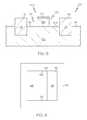
- FINFET IC 100begins as illustrated in cross section in FIG. 1 with the provision of a silicon substrate or wafer 102 .
- a thin layer of pad oxide 104is formed on upper surface 106 of the substrate.
- a layer of silicon nitride 108is deposited overlying the pad oxide.
- the layer of pad oxide and the layer of silicon nitrideare patterned using conventional photolithography and etch techniques to expose a portion of the substrate in which shallow trench isolation (STI) 110 is to be formed as described in the following.
- STIshallow trench isolation
- STI 110defines a device region 112 in the substrate and provides electrical isolation between devices as is required by the circuit design. As illustrated in the following, only one FINFET is to be fabricated in device region 112 . There will be many such device regions in IC 100 and any number of FINFETs may be fabricated in some of those device regions.
- the patterned silicon nitride layer 108is used as a hard etch mask and trenches 114 are etched into the silicon substrate. The trenches are filled with a dielectric material 116 such as a silicon oxide to provide electrical isolation between device region 112 and similar device regions outside the STI.
- the methodcontinues by planarizing dielectric material 116 that fills trenches 114 .
- the dielectric materialcan be planarized, for example by chemical mechanical planarization (CMP) using nitride layer 108 as a polish stop.
- CMPchemical mechanical planarization
- Dielectric material 116protrudes above surface 106 by an amount substantially equal to the total thickness of pad oxide 104 and silicon nitride 108 .
- a layer 118 of silicon germanium (SiGe) or other crystalline materialis epitaxially grown on surface 106 within device region 112 by a process of selective epitaxial growth as illustrated in FIG. 4 .
- a layer of silicon 120is epitaxially grown overlying the layer of SiGe, also by a process of selective epitaxial growth.
- the growth conditions and reactantsare adjusted so that the material layer being grown grows only on crystalline material and does not grow on non-crystalline materials such as dielectric material 116 .
- Layer 118 of SiGepreferably contains at least 20% germanium and has a thickness of a few tens of nanometers (nm). Layer 118 can be, for example about 10-30 nm.
- the thickness of layer of silicon 120determines the height of the fin that is to be formed.
- the height of the finis determined by the desired transistor characteristics of the integrated circuit being fabricated, but can be, for example, between about 25 nm and 125 nm and preferably about 100 nm.
- the total height of layers 118 and 120 togetherare preferably substantially the same as the height that dielectric material 116 protrudes above surface 106 .
- Layer of silicon 120can be undoped or can be doped with conductivity determining impurities depending on the desired characteristics of the channel region of FINFET 200 .
- a layer of hard mask material 122such as a layer of silicon nitride is deposited overlying layer 120 of silicon.
- crystalline material besides SiGecan be used as the crystalline layer underlying layer 120 of silicon providing the material is differentially etchable with respect to silicon (i.e., a material etchant exists that etches silicon at a much lower rate than the etch rate of the material and a silicon etchant exists that etches the material at much lower etch rate than the etch rate of silicon) and providing the crystalline nature of the material is such that a high quality crystalline layer of silicon can be grown on that material.
- alignment marksare etched in the surface of the wafer, the epitaxial layers are grown, and then the STI is formed. This embodiment has the advantage that the epitaxial layers are grown on a flat surface without pattern loading effects.
- the method for fabricating FINFET IC 100continues, in accordance with one embodiment, by patterning hard mask layer 122 using conventional photolithographic and etch techniques.
- the patterned hard mask layeris used as an etch mask and layer 120 of silicon is etched to form a fin 124 .
- the layer of siliconis etched using an anisotropic etch process such as reactive ion etching (RIE) using an etchant such as a mixture of O 2 , N 2 , and CH 2 F 2 that etches silicon at a substantially higher etch rate than the etch rate of silicon germanium.
- RIEreactive ion etching
- the layer of silicon germaniumthus acts as an etch stop and the height of fin 124 is determined solely by the thickness of the epitaxial layer of silicon.
- Epitaxial growthis an atomic-layer-by-atomic-layer growth process that can be precisely controlled, so the thickness of layer 120 and the height of fin 124 can be precisely controlled.
- FIG. 6illustrates FINFET 100 in plan view. Fin 124 extends across device region 112 with the ends 126 of the fin abutting STI 110 . Patterned hard mask 122 is removed in an etchant that preferentially etches the hard mask material but not the silicon or silicon germanium. If the hard mask material is silicon nitride, for example, the silicon nitride can be removed in hot phosphoric acid.
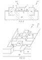
- SiGe layer 118is removed as illustrated in FIG. 7 to create a void 128 underlying fin 124 .
- SiGe layer 118is removed by etching in an etchant that etches SiGe at a substantially faster etch rate than the etch rate of the silicon of fin 124 or the silicon oxide or other insulating material filling STI 110 .
- the SiGecan be etched, for example, in a gaseous mixture of hydrochloric acid and hydrogen, in an aqueous solution of hydrofluoric acid, nitric acid and acetic acid, or in a plasma CF 4 etchant.
- fin 124is substantially unaffected.
- fin 124appears to be floating above void 128 . Fin 124 , however, is supported at ends 126 as they contact STI 110 .
- the void underlying fin 124is filled with a dielectric insulating material 130 such as silicon oxide, silicon nitride, or mixtures thereof.
- the dielectric materialcan be deposited by chemical vapor deposition (CVD) or, preferably, by atomic layer deposition (ALD). Especially if the dielectric material is deposited by ALD, the layer is substantially conformal.
- the dielectric materialmust be removed from the sidewalls 132 and top surface 134 of fin 124 because that is where the channel of FINFET 200 will be formed.
- a planarizing layer 140such as an organic planarizing layer (OPL) is applied overlying dielectric material 130 .
- OPLorganic planarizing layer
- OPLis spun on as a liquid and is subsequently cured to form a solid having a planar upper layer.
- a thick layer of materialcan be deposited, for example by CVD and subsequently planarized by CMP.
- the material selected for planarizing layer 140is a material having substantially the same etch rate as the etch rate of dielectric material 130 and a substantially faster etch rate than the etch rate of the silicon fin.
- Planarizing layer 140 and dielectric material 130are anisotropically etched, for example by reactive ion etching (RIE) to remove the dielectric material from the sidewalls and top surface of fin 124 as illustrated in FIG. 9 .
- the etchingis stopped when the dielectric material has been removed from the sidewalls and the top surface.
- a layer 136 of dielectric materialremains overlying the exposed portion of surface 106 and filling void 128 underlying fin 124 .
- Layer 136supports fin 124 and electrically isolates the fin from substrate 102 . Fin 124 is thus electrically isolated from other devices and from other fins by layer 136 and by STI 110 .
- FIG. 10is a partially cut away perspective view of FINFET 200 .
- a gate structure 146is formed overlying fin 124 .
- the gate structureincludes a layer of gate dielectric material and a gate electrode.
- a layer of gate dielectric material(not illustrated) such as silicon oxide, a high dielectric constant (high k) insulator, or combinations thereof is deposited or otherwise formed overlying fin 124 .
- a layer of gate electrode forming materialis deposited overlying the gate dielectric material and is patterned to form a gate electrode 150 .
- gate electrode 150can extend onto and over STI 110 .
- the gate electrode materialcan be polycrystalline silicon, a metal or other conductive material and may also include a work function determining layer.
- the gate electrode structuremay also include sidewall spacers formed on the sidewalls of the gate electrode in conventional manner.
- the method for fabricating FINFET ICcontinues in conventional manner by impurity doping the end portions 160 , 170 of fin 124 with conductivity determining impurities to form source and drain regions.
- the impurity dopingcan be done by ion implantation or by plasma doping, with either doping technique using the gate structure as a doping mask so that the source and drain regions are self aligned to the gate structure.
- Contacts to the source and drain regionscan also be formed in conventional manner, for example by depositing a layer of insulating material, etching openings through the insulating material to expose portions of the source and drain regions, and filling the openings with metal or other conductive material.
- a layer of crystalline material 118such as a layer of SiGe is removed ( FIG. 7 ) to create a void 128 underlying fin 124 and is replaced by a dielectric layer 130 that fills the void ( FIG. 8 ).
- a gate structure 146is then formed overlying fin 124 ( FIG. 10 ).
- gate structure 146can be formed overlying fin 124 before the layer of crystalline material 118 is removed.
- the layer of dielectric material 130is then deposited to fill void 128 and to underlie gate structure 146 .
- Excess portions of the layer of dielectric materialcan then be removed, for example by RIE, to form sidewall spacers on the sidewalls of gate structure 146 , leaving a remaining layer of dielectric material 136 underlying and supporting fin 124 and gate structure 146 .
Landscapes
- Engineering & Computer Science (AREA)
- Physics & Mathematics (AREA)
- Plasma & Fusion (AREA)
- Condensed Matter Physics & Semiconductors (AREA)
- General Physics & Mathematics (AREA)
- Manufacturing & Machinery (AREA)
- Computer Hardware Design (AREA)
- Microelectronics & Electronic Packaging (AREA)
- Power Engineering (AREA)
- Thin Film Transistor (AREA)
- Metal-Oxide And Bipolar Metal-Oxide Semiconductor Integrated Circuits (AREA)
Abstract
Description
- The present invention generally relates to methods for manufacturing integrated circuits, and more particularly relates to methods for manufacturing FINFET integrated circuits on bulk silicon substrates.
- Transistors such as metal oxide semiconductor field effect transistors (MOSFETs) or simply field effect transistors (FETs) or MOS transistors are the core building blocks of the vast majority of semiconductor integrated circuits (ICs). A FET includes source and drain regions between which a current can flow through a channel under the influence of a bias applied to a gate electrode that overlies the channel. Some semiconductor ICs, such as high performance microprocessors, can include millions of FETs. For such ICs, decreasing transistor size and thus increasing transistor density has traditionally been a high priority in the semiconductor manufacturing industry. Transistor performance, however, must be maintained even as the transistor size decreases.
- A FINFET is a type of transistor that lends itself to the dual goals of reducing transistor size while maintaining transistor performance. The FINFET is a three dimensional transistor formed in a thin fin that extends upwardly from a semiconductor substrate. Transistor performance, often measured by its transconductance, is proportional to the width of the transistor channel. In a FINFET the transistor channel is formed at least along the vertical sidewalls of the fin, so a wide channel, and hence high performance, can be achieved without substantially increasing the area of the substrate surface required by the transistor.
- Many FINFET ICs are fabricated on semiconductor-on-insulator (SOI) substrates because of the easy isolation provided by the buried oxide layer. SOI substrates are expensive, however, so there are significant economic advantages to fabricating the ICs on bulk wafers. A number of techniques have been attempted to provide isolation between fins of a bulk wafer FINFET IC, but such attempts have had limited success. Among the disadvantages of such isolation techniques are processing difficulties, complicated processing, and, most importantly, variability of the final height of the fin. The height of the fin determines the width of the transistor channel which, in turn, determines the drive capability of the transistor. Variability in fin height thus makes it difficult to reproducibly fabricate transistors having the device characteristics needed for the circuit being implemented.
- Accordingly, it is desirable to provide methods for fabricating FINFET ICs having fins of predetermined and reproducible height. In addition, it is desirable to provide methods for fabricating FINFET ICs having dielectric isolation between fins. Furthermore, other desirable features and characteristics of the present invention will become apparent from the subsequent detailed description and the appended claims, taken in conjunction with the accompanying drawings and the foregoing technical field and background.
- Methods are provided for fabricating FINFET integrated circuits on a bulk substrate. In accordance with one embodiment a method includes epitaxially growing a first silicon germanium layer and a second silicon layer overlying a silicon substrate. The second silicon layer is etched to form a silicon fin using the first silicon germanium layer as an etch stop. The first silicon germanium layer underlying the fin is removed to form a void underlying the fin and the void is filled with an insulating material. A gate structure is then formed overlying the fin.
- In accordance with another embodiment a method for fabricating a FINFET integrated circuit includes growing a silicon germanium epitaxial layer overlying a silicon substrate and growing a silicon epitaxial layer overlying the silicon germanium epitaxial layer. Shallow trench isolation is formed to define a device region. The silicon epitaxial layer is etched in an etchant that etches silicon at a substantially higher etch rate than the etch rate of silicon germanium to form a silicon fin extending across the device region and contacting the shallow trench isolation. The silicon germanium epitaxial layer is etched in an etchant that etches silicon germanium at a substantially higher etch rate than the etch rate of silicon to form a void underlying the silicon fin. A dielectric is deposited overlying the silicon fin and filling the void, and a planarizing layer is deposited overlying the dielectric. The planarizing layer and the dielectric are etched to remove the dielectric overlying the silicon fin and a gate dielectric and a gate electrode are formed overlying the silicon fin.
- In accordance with yet another embodiment a method for fabricating a FINFET integrated circuit includes forming a shallow trench isolation defining a device region in a silicon substrate. A first crystalline layer is formed overlying the substrate and a silicon layer is formed overlying the first crystalline layer. The silicon layer is patterned to form a fin extending across the device region and contacting the shallow trench isolation. A gate structure is formed overlying the fin. The first crystalline layer underlying the fin is removed and a dielectric layer is deposited underlying and supporting the fin.
- The present invention will hereinafter be described in conjunction with the following drawing figures, wherein like numerals denote like elements, and wherein:
FIGS. 1-10 illustrate methods for fabricating a FINFET IC in accordance with various embodiments.FIGS. 1-5 and7-9 are cross sectional views;FIG. 6 is a plan view; andFIG. 10 is a partially cut away perspective view.- The following detailed description is merely exemplary in nature and is not intended to limit the invention or the application and uses of the invention. Furthermore, there is no intention to be bound by any expressed or implied theory presented in the preceding technical field, background, brief summary or the following detailed description.
FIGS. 1-10 illustrate method steps for fabricating a FINFET integrated circuit (IC)100 in accordance with various embodiments. The described process steps, procedures, and materials are to be considered only as exemplary embodiments designed to illustrate to one of ordinary skill in the art methods for practicing the invention; the invention is not to be limited to these exemplary embodiments. Various steps in the manufacture of ICs are well known and so, in the interest of brevity, many conventional steps will only be mentioned briefly herein or will be omitted entirely without providing the well known process details. The FIGURES illustrate only asingle FINFET 200 ofIC 100 although those of skill in the art will understand the IC may contains a large number of such devices as required by the circuit being implemented.- The fabrication of FINFET IC100, in accordance with one embodiment, begins as illustrated in cross section in
FIG. 1 with the provision of a silicon substrate orwafer 102. A thin layer ofpad oxide 104 is formed onupper surface 106 of the substrate. A layer ofsilicon nitride 108 is deposited overlying the pad oxide. The layer of pad oxide and the layer of silicon nitride are patterned using conventional photolithography and etch techniques to expose a portion of the substrate in which shallow trench isolation (STI)110 is to be formed as described in the following. - As illustrated in
FIG. 2 , STI110 defines adevice region 112 in the substrate and provides electrical isolation between devices as is required by the circuit design. As illustrated in the following, only one FINFET is to be fabricated indevice region 112. There will be many such device regions in IC100 and any number of FINFETs may be fabricated in some of those device regions. The patternedsilicon nitride layer 108 is used as a hard etch mask andtrenches 114 are etched into the silicon substrate. The trenches are filled with adielectric material 116 such as a silicon oxide to provide electrical isolation betweendevice region 112 and similar device regions outside the STI. The method continues by planarizingdielectric material 116 that fills trenches114. The dielectric material can be planarized, for example by chemical mechanical planarization (CMP) usingnitride layer 108 as a polish stop. - Following the planarization the remaining silicon nitride and pad oxide are removed and the remaining portion of
surface 106 withindevice region 112 is cleaned as illustrated inFIG. 3 .Dielectric material 116 protrudes abovesurface 106 by an amount substantially equal to the total thickness ofpad oxide 104 andsilicon nitride 108. - In accordance with one embodiment a
layer 118 of silicon germanium (SiGe) or other crystalline material is epitaxially grown onsurface 106 withindevice region 112 by a process of selective epitaxial growth as illustrated inFIG. 4 . A layer ofsilicon 120 is epitaxially grown overlying the layer of SiGe, also by a process of selective epitaxial growth. In the process of selective epitaxial growth the growth conditions and reactants are adjusted so that the material layer being grown grows only on crystalline material and does not grow on non-crystalline materials such asdielectric material 116.Layer 118 of SiGe preferably contains at least 20% germanium and has a thickness of a few tens of nanometers (nm).Layer 118 can be, for example about 10-30 nm. The thickness of layer ofsilicon 120 determines the height of the fin that is to be formed. The height of the fin is determined by the desired transistor characteristics of the integrated circuit being fabricated, but can be, for example, between about 25 nm and 125 nm and preferably about 100 nm. The total height oflayers dielectric material 116 protrudes abovesurface 106. Layer ofsilicon 120 can be undoped or can be doped with conductivity determining impurities depending on the desired characteristics of the channel region ofFINFET 200. A layer ofhard mask material 122 such as a layer of silicon nitride is depositedoverlying layer 120 of silicon. Other crystalline material besides SiGe can be used as the crystalline layerunderlying layer 120 of silicon providing the material is differentially etchable with respect to silicon (i.e., a material etchant exists that etches silicon at a much lower rate than the etch rate of the material and a silicon etchant exists that etches the material at much lower etch rate than the etch rate of silicon) and providing the crystalline nature of the material is such that a high quality crystalline layer of silicon can be grown on that material. Although not illustrated, in an alternate embodiment, alignment marks are etched in the surface of the wafer, the epitaxial layers are grown, and then the STI is formed. This embodiment has the advantage that the epitaxial layers are grown on a flat surface without pattern loading effects. - As illustrated in
FIG. 5 , the method for fabricatingFINFET IC 100 continues, in accordance with one embodiment, by patterninghard mask layer 122 using conventional photolithographic and etch techniques. The patterned hard mask layer is used as an etch mask andlayer 120 of silicon is etched to form afin 124. The layer of silicon is etched using an anisotropic etch process such as reactive ion etching (RIE) using an etchant such as a mixture of O2, N2, and CH2F2that etches silicon at a substantially higher etch rate than the etch rate of silicon germanium. The layer of silicon germanium thus acts as an etch stop and the height offin 124 is determined solely by the thickness of the epitaxial layer of silicon. Epitaxial growth is an atomic-layer-by-atomic-layer growth process that can be precisely controlled, so the thickness oflayer 120 and the height offin 124 can be precisely controlled.FIG. 6 illustratesFINFET 100 in plan view.Fin 124 extends acrossdevice region 112 with theends 126 of thefin abutting STI 110. Patternedhard mask 122 is removed in an etchant that preferentially etches the hard mask material but not the silicon or silicon germanium. If the hard mask material is silicon nitride, for example, the silicon nitride can be removed in hot phosphoric acid. - After etching
layer 120 of silicon to formfin 124,SiGe layer 118 is removed as illustrated inFIG. 7 to create a void128underlying fin 124.SiGe layer 118 is removed by etching in an etchant that etches SiGe at a substantially faster etch rate than the etch rate of the silicon offin 124 or the silicon oxide or other insulatingmaterial filling STI 110. The SiGe can be etched, for example, in a gaseous mixture of hydrochloric acid and hydrogen, in an aqueous solution of hydrofluoric acid, nitric acid and acetic acid, or in a plasma CF4etchant. Again, because the selected etchant has a very low etch rate for silicon, the height offin 124 is substantially unaffected. In the cross sectional view ofFIG. 7 fin 124 appears to be floating abovevoid 128.Fin 124, however, is supported at ends126 as they contactSTI 110. - As illustrated in
FIG. 8 , the voidunderlying fin 124 is filled with a dielectric insulatingmaterial 130 such as silicon oxide, silicon nitride, or mixtures thereof. The dielectric material can be deposited by chemical vapor deposition (CVD) or, preferably, by atomic layer deposition (ALD). Especially if the dielectric material is deposited by ALD, the layer is substantially conformal. The dielectric material must be removed from thesidewalls 132 andtop surface 134 offin 124 because that is where the channel ofFINFET 200 will be formed. To aid in removingdielectric material 130, aplanarizing layer 140 such as an organic planarizing layer (OPL) is applied overlyingdielectric material 130. OPL is spun on as a liquid and is subsequently cured to form a solid having a planar upper layer. Alternatively, a thick layer of material can be deposited, for example by CVD and subsequently planarized by CMP. In accordance with either alternative the material selected forplanarizing layer 140 is a material having substantially the same etch rate as the etch rate ofdielectric material 130 and a substantially faster etch rate than the etch rate of the silicon fin. Planarizing layer 140 anddielectric material 130 are anisotropically etched, for example by reactive ion etching (RIE) to remove the dielectric material from the sidewalls and top surface offin 124 as illustrated inFIG. 9 . The etching is stopped when the dielectric material has been removed from the sidewalls and the top surface. Alayer 136 of dielectric material remains overlying the exposed portion ofsurface 106 and fillingvoid 128underlying fin 124.Layer 136 supportsfin 124 and electrically isolates the fin fromsubstrate 102.Fin 124 is thus electrically isolated from other devices and from other fins bylayer 136 and bySTI 110.- The method for fabricating
FINFET IC 100 in accordance with one embodiment continues as illustrated inFIG. 10 which is a partially cut away perspective view ofFINFET 200. Agate structure 146 is formedoverlying fin 124. The gate structure includes a layer of gate dielectric material and a gate electrode. A layer of gate dielectric material (not illustrated) such as silicon oxide, a high dielectric constant (high k) insulator, or combinations thereof is deposited or otherwise formedoverlying fin 124. A layer of gate electrode forming material is deposited overlying the gate dielectric material and is patterned to form agate electrode 150. Although not so illustrated,gate electrode 150 can extend onto and overSTI 110. The gate electrode material can be polycrystalline silicon, a metal or other conductive material and may also include a work function determining layer. The gate electrode structure may also include sidewall spacers formed on the sidewalls of the gate electrode in conventional manner. - Although not illustrated, the method for fabricating FINFET IC continues in conventional manner by impurity doping the
end portions fin 124 with conductivity determining impurities to form source and drain regions. The impurity doping can be done by ion implantation or by plasma doping, with either doping technique using the gate structure as a doping mask so that the source and drain regions are self aligned to the gate structure. Contacts to the source and drain regions can also be formed in conventional manner, for example by depositing a layer of insulating material, etching openings through the insulating material to expose portions of the source and drain regions, and filling the openings with metal or other conductive material. - In the above-described embodiments a layer of
crystalline material 118 such as a layer of SiGe is removed (FIG. 7 ) to create a void128underlying fin 124 and is replaced by adielectric layer 130 that fills the void (FIG. 8 ). Agate structure 146 is then formed overlying fin124 (FIG. 10 ). Although not illustrated,gate structure 146 can be formedoverlying fin 124 before the layer ofcrystalline material 118 is removed. The layer ofdielectric material 130 is then deposited to fillvoid 128 and to underliegate structure 146. Excess portions of the layer of dielectric material can then be removed, for example by RIE, to form sidewall spacers on the sidewalls ofgate structure 146, leaving a remaining layer ofdielectric material 136 underlying and supportingfin 124 andgate structure 146. - While at least one exemplary embodiment has been presented in the foregoing detailed description, it should be appreciated that a vast number of variations exist. It should also be appreciated that the exemplary embodiments are only examples, and are not intended to limit the scope, applicability, or configuration of the invention in any way. Rather, the foregoing detailed description will provide those skilled in the art with a convenient road map for implementing the exemplary embodiments. It should be understood that various changes can be made in the function and arrangement of elements without departing from the scope of the invention as set forth in the appended claims and the legal equivalents thereof.
Claims (20)
Priority Applications (1)
| Application Number | Priority Date | Filing Date | Title |
|---|---|---|---|
| US13/172,635US8637372B2 (en) | 2011-06-29 | 2011-06-29 | Methods for fabricating a FINFET integrated circuit on a bulk silicon substrate |
Applications Claiming Priority (1)
| Application Number | Priority Date | Filing Date | Title |
|---|---|---|---|
| US13/172,635US8637372B2 (en) | 2011-06-29 | 2011-06-29 | Methods for fabricating a FINFET integrated circuit on a bulk silicon substrate |
Publications (2)
| Publication Number | Publication Date |
|---|---|
| US20130005103A1true US20130005103A1 (en) | 2013-01-03 |
| US8637372B2 US8637372B2 (en) | 2014-01-28 |
Family
ID=47391072
Family Applications (1)
| Application Number | Title | Priority Date | Filing Date |
|---|---|---|---|
| US13/172,635Expired - Fee RelatedUS8637372B2 (en) | 2011-06-29 | 2011-06-29 | Methods for fabricating a FINFET integrated circuit on a bulk silicon substrate |
Country Status (1)
| Country | Link |
|---|---|
| US (1) | US8637372B2 (en) |
Cited By (143)
| Publication number | Priority date | Publication date | Assignee | Title |
|---|---|---|---|---|
| US20140027863A1 (en)* | 2012-07-30 | 2014-01-30 | International Business Machines Corporation | Merged fin finfet with (100) sidewall surfaces and method of making same |
| US20140353763A1 (en)* | 2013-06-03 | 2014-12-04 | Samsung Electronics Co., Ltd. | Semiconductor devices including fin-fets and methods of fabricating the same |
| US8951850B1 (en) | 2013-08-21 | 2015-02-10 | International Business Machines Corporation | FinFET formed over dielectric |
| US20150126040A1 (en)* | 2013-11-04 | 2015-05-07 | Applied Materials, Inc. | Silicon germanium processing |
| US9070770B2 (en) | 2013-08-27 | 2015-06-30 | International Business Machines Corporation | Low interfacial defect field effect transistor |
| US20150221769A1 (en)* | 2012-08-10 | 2015-08-06 | Institute of Microelectronics, Chinese Academy of Sciences | Finfet and method for manufacturing the same |
| US9224866B2 (en) | 2013-08-27 | 2015-12-29 | Globalfoundries Inc. | Suspended body field effect transistor |
| US9257537B2 (en) | 2013-12-27 | 2016-02-09 | International Business Machines Corporation | Finfet including improved epitaxial topology |
| US9269590B2 (en) | 2014-04-07 | 2016-02-23 | Applied Materials, Inc. | Spacer formation |
| US9287134B2 (en) | 2014-01-17 | 2016-03-15 | Applied Materials, Inc. | Titanium oxide etch |
| US9287095B2 (en) | 2013-12-17 | 2016-03-15 | Applied Materials, Inc. | Semiconductor system assemblies and methods of operation |
| US9293568B2 (en) | 2014-01-27 | 2016-03-22 | Applied Materials, Inc. | Method of fin patterning |
| US9299583B1 (en) | 2014-12-05 | 2016-03-29 | Applied Materials, Inc. | Aluminum oxide selective etch |
| US9299537B2 (en) | 2014-03-20 | 2016-03-29 | Applied Materials, Inc. | Radial waveguide systems and methods for post-match control of microwaves |
| US9299538B2 (en) | 2014-03-20 | 2016-03-29 | Applied Materials, Inc. | Radial waveguide systems and methods for post-match control of microwaves |
| US9299575B2 (en) | 2014-03-17 | 2016-03-29 | Applied Materials, Inc. | Gas-phase tungsten etch |
| US9309598B2 (en) | 2014-05-28 | 2016-04-12 | Applied Materials, Inc. | Oxide and metal removal |
| US9324576B2 (en) | 2010-05-27 | 2016-04-26 | Applied Materials, Inc. | Selective etch for silicon films |
| US9343272B1 (en) | 2015-01-08 | 2016-05-17 | Applied Materials, Inc. | Self-aligned process |
| US9349863B2 (en) | 2013-08-07 | 2016-05-24 | Globalfoundries Inc. | Anchored stress-generating active semiconductor regions for semiconductor-on-insulator finfet |
| US9349605B1 (en) | 2015-08-07 | 2016-05-24 | Applied Materials, Inc. | Oxide etch selectivity systems and methods |
| US9355863B2 (en) | 2012-12-18 | 2016-05-31 | Applied Materials, Inc. | Non-local plasma oxide etch |
| US9355856B2 (en) | 2014-09-12 | 2016-05-31 | Applied Materials, Inc. | V trench dry etch |
| US9355862B2 (en) | 2014-09-24 | 2016-05-31 | Applied Materials, Inc. | Fluorine-based hardmask removal |
| US9362130B2 (en) | 2013-03-01 | 2016-06-07 | Applied Materials, Inc. | Enhanced etching processes using remote plasma sources |
| US9368364B2 (en) | 2014-09-24 | 2016-06-14 | Applied Materials, Inc. | Silicon etch process with tunable selectivity to SiO2 and other materials |
| US9373522B1 (en) | 2015-01-22 | 2016-06-21 | Applied Mateials, Inc. | Titanium nitride removal |
| US9373517B2 (en) | 2012-08-02 | 2016-06-21 | Applied Materials, Inc. | Semiconductor processing with DC assisted RF power for improved control |
| US9378969B2 (en) | 2014-06-19 | 2016-06-28 | Applied Materials, Inc. | Low temperature gas-phase carbon removal |
| US9378978B2 (en) | 2014-07-31 | 2016-06-28 | Applied Materials, Inc. | Integrated oxide recess and floating gate fin trimming |
| US9384997B2 (en) | 2012-11-20 | 2016-07-05 | Applied Materials, Inc. | Dry-etch selectivity |
| US9385028B2 (en) | 2014-02-03 | 2016-07-05 | Applied Materials, Inc. | Air gap process |
| US9390937B2 (en) | 2012-09-20 | 2016-07-12 | Applied Materials, Inc. | Silicon-carbon-nitride selective etch |
| US9396989B2 (en) | 2014-01-27 | 2016-07-19 | Applied Materials, Inc. | Air gaps between copper lines |
| US9406523B2 (en) | 2014-06-19 | 2016-08-02 | Applied Materials, Inc. | Highly selective doped oxide removal method |
| US9412608B2 (en) | 2012-11-30 | 2016-08-09 | Applied Materials, Inc. | Dry-etch for selective tungsten removal |
| US9418902B2 (en) | 2013-10-10 | 2016-08-16 | Globalfoundries Inc. | Forming isolated fins from a substrate |
| US9418858B2 (en) | 2011-10-07 | 2016-08-16 | Applied Materials, Inc. | Selective etch of silicon by way of metastable hydrogen termination |
| US9425058B2 (en) | 2014-07-24 | 2016-08-23 | Applied Materials, Inc. | Simplified litho-etch-litho-etch process |
| US9437451B2 (en) | 2012-09-18 | 2016-09-06 | Applied Materials, Inc. | Radical-component oxide etch |
| US9449850B2 (en) | 2013-03-15 | 2016-09-20 | Applied Materials, Inc. | Processing systems and methods for halide scavenging |
| US9449845B2 (en) | 2012-12-21 | 2016-09-20 | Applied Materials, Inc. | Selective titanium nitride etching |
| US9449846B2 (en) | 2015-01-28 | 2016-09-20 | Applied Materials, Inc. | Vertical gate separation |
| US9472412B2 (en) | 2013-12-02 | 2016-10-18 | Applied Materials, Inc. | Procedure for etch rate consistency |
| US9472417B2 (en) | 2013-11-12 | 2016-10-18 | Applied Materials, Inc. | Plasma-free metal etch |
| US9478432B2 (en) | 2014-09-25 | 2016-10-25 | Applied Materials, Inc. | Silicon oxide selective removal |
| US9496167B2 (en) | 2014-07-31 | 2016-11-15 | Applied Materials, Inc. | Integrated bit-line airgap formation and gate stack post clean |
| US9493879B2 (en) | 2013-07-12 | 2016-11-15 | Applied Materials, Inc. | Selective sputtering for pattern transfer |
| US9502258B2 (en) | 2014-12-23 | 2016-11-22 | Applied Materials, Inc. | Anisotropic gap etch |
| US9499898B2 (en) | 2014-03-03 | 2016-11-22 | Applied Materials, Inc. | Layered thin film heater and method of fabrication |
| US9543297B1 (en)* | 2015-09-29 | 2017-01-10 | Globalfoundries Inc. | Fin-FET replacement metal gate structure and method of manufacturing the same |
| US9553102B2 (en) | 2014-08-19 | 2017-01-24 | Applied Materials, Inc. | Tungsten separation |
| US9576809B2 (en) | 2013-11-04 | 2017-02-21 | Applied Materials, Inc. | Etch suppression with germanium |
| US9607856B2 (en) | 2013-03-05 | 2017-03-28 | Applied Materials, Inc. | Selective titanium nitride removal |
| US9614057B2 (en) | 2014-12-30 | 2017-04-04 | International Business Machines Corporation | Enriched, high mobility strained fin having bottom dielectric isolation |
| US9659753B2 (en) | 2014-08-07 | 2017-05-23 | Applied Materials, Inc. | Grooved insulator to reduce leakage current |
| US9691645B2 (en) | 2015-08-06 | 2017-06-27 | Applied Materials, Inc. | Bolted wafer chuck thermal management systems and methods for wafer processing systems |
| US9721789B1 (en) | 2016-10-04 | 2017-08-01 | Applied Materials, Inc. | Saving ion-damaged spacers |
| US9728437B2 (en) | 2015-02-03 | 2017-08-08 | Applied Materials, Inc. | High temperature chuck for plasma processing systems |
| US9741593B2 (en) | 2015-08-06 | 2017-08-22 | Applied Materials, Inc. | Thermal management systems and methods for wafer processing systems |
| US9768034B1 (en) | 2016-11-11 | 2017-09-19 | Applied Materials, Inc. | Removal methods for high aspect ratio structures |
| US9773648B2 (en) | 2013-08-30 | 2017-09-26 | Applied Materials, Inc. | Dual discharge modes operation for remote plasma |
| US9842744B2 (en) | 2011-03-14 | 2017-12-12 | Applied Materials, Inc. | Methods for etch of SiN films |
| US9865484B1 (en) | 2016-06-29 | 2018-01-09 | Applied Materials, Inc. | Selective etch using material modification and RF pulsing |
| US9881805B2 (en) | 2015-03-02 | 2018-01-30 | Applied Materials, Inc. | Silicon selective removal |
| US9885117B2 (en) | 2014-03-31 | 2018-02-06 | Applied Materials, Inc. | Conditioned semiconductor system parts |
| US9887096B2 (en) | 2012-09-17 | 2018-02-06 | Applied Materials, Inc. | Differential silicon oxide etch |
| US9934942B1 (en) | 2016-10-04 | 2018-04-03 | Applied Materials, Inc. | Chamber with flow-through source |
| US9947549B1 (en) | 2016-10-10 | 2018-04-17 | Applied Materials, Inc. | Cobalt-containing material removal |
| US9978564B2 (en) | 2012-09-21 | 2018-05-22 | Applied Materials, Inc. | Chemical control features in wafer process equipment |
| US10026621B2 (en) | 2016-11-14 | 2018-07-17 | Applied Materials, Inc. | SiN spacer profile patterning |
| US10043684B1 (en) | 2017-02-06 | 2018-08-07 | Applied Materials, Inc. | Self-limiting atomic thermal etching systems and methods |
| US10043674B1 (en) | 2017-08-04 | 2018-08-07 | Applied Materials, Inc. | Germanium etching systems and methods |
| US10049891B1 (en) | 2017-05-31 | 2018-08-14 | Applied Materials, Inc. | Selective in situ cobalt residue removal |
| US10062587B2 (en) | 2012-07-18 | 2018-08-28 | Applied Materials, Inc. | Pedestal with multi-zone temperature control and multiple purge capabilities |
| US10062579B2 (en) | 2016-10-07 | 2018-08-28 | Applied Materials, Inc. | Selective SiN lateral recess |
| US10062578B2 (en) | 2011-03-14 | 2018-08-28 | Applied Materials, Inc. | Methods for etch of metal and metal-oxide films |
| US10062585B2 (en) | 2016-10-04 | 2018-08-28 | Applied Materials, Inc. | Oxygen compatible plasma source |
| US10062575B2 (en) | 2016-09-09 | 2018-08-28 | Applied Materials, Inc. | Poly directional etch by oxidation |
| US10128086B1 (en) | 2017-10-24 | 2018-11-13 | Applied Materials, Inc. | Silicon pretreatment for nitride removal |
| US10163696B2 (en) | 2016-11-11 | 2018-12-25 | Applied Materials, Inc. | Selective cobalt removal for bottom up gapfill |
| US10170336B1 (en) | 2017-08-04 | 2019-01-01 | Applied Materials, Inc. | Methods for anisotropic control of selective silicon removal |
| US10224210B2 (en) | 2014-12-09 | 2019-03-05 | Applied Materials, Inc. | Plasma processing system with direct outlet toroidal plasma source |
| US10242908B2 (en) | 2016-11-14 | 2019-03-26 | Applied Materials, Inc. | Airgap formation with damage-free copper |
| US10256112B1 (en) | 2017-12-08 | 2019-04-09 | Applied Materials, Inc. | Selective tungsten removal |
| US10256079B2 (en) | 2013-02-08 | 2019-04-09 | Applied Materials, Inc. | Semiconductor processing systems having multiple plasma configurations |
| US10283321B2 (en) | 2011-01-18 | 2019-05-07 | Applied Materials, Inc. | Semiconductor processing system and methods using capacitively coupled plasma |
| US10283324B1 (en) | 2017-10-24 | 2019-05-07 | Applied Materials, Inc. | Oxygen treatment for nitride etching |
| US10297458B2 (en) | 2017-08-07 | 2019-05-21 | Applied Materials, Inc. | Process window widening using coated parts in plasma etch processes |
| US10319739B2 (en) | 2017-02-08 | 2019-06-11 | Applied Materials, Inc. | Accommodating imperfectly aligned memory holes |
| US10319600B1 (en) | 2018-03-12 | 2019-06-11 | Applied Materials, Inc. | Thermal silicon etch |
| US10319649B2 (en) | 2017-04-11 | 2019-06-11 | Applied Materials, Inc. | Optical emission spectroscopy (OES) for remote plasma monitoring |
| US10354889B2 (en) | 2017-07-17 | 2019-07-16 | Applied Materials, Inc. | Non-halogen etching of silicon-containing materials |
| WO2019139572A1 (en)* | 2018-01-10 | 2019-07-18 | Intel Corporation | Bottom fin trim isolation aligned with top gate for stacked device architectures |
| US10403507B2 (en) | 2017-02-03 | 2019-09-03 | Applied Materials, Inc. | Shaped etch profile with oxidation |
| US10431429B2 (en) | 2017-02-03 | 2019-10-01 | Applied Materials, Inc. | Systems and methods for radial and azimuthal control of plasma uniformity |
| US10468267B2 (en) | 2017-05-31 | 2019-11-05 | Applied Materials, Inc. | Water-free etching methods |
| US10490406B2 (en) | 2018-04-10 | 2019-11-26 | Appled Materials, Inc. | Systems and methods for material breakthrough |
| US10490418B2 (en) | 2014-10-14 | 2019-11-26 | Applied Materials, Inc. | Systems and methods for internal surface conditioning assessment in plasma processing equipment |
| US10497573B2 (en) | 2018-03-13 | 2019-12-03 | Applied Materials, Inc. | Selective atomic layer etching of semiconductor materials |
| US10504754B2 (en) | 2016-05-19 | 2019-12-10 | Applied Materials, Inc. | Systems and methods for improved semiconductor etching and component protection |
| US10504700B2 (en) | 2015-08-27 | 2019-12-10 | Applied Materials, Inc. | Plasma etching systems and methods with secondary plasma injection |
| US10522371B2 (en) | 2016-05-19 | 2019-12-31 | Applied Materials, Inc. | Systems and methods for improved semiconductor etching and component protection |
| US10541184B2 (en) | 2017-07-11 | 2020-01-21 | Applied Materials, Inc. | Optical emission spectroscopic techniques for monitoring etching |
| US10541246B2 (en) | 2017-06-26 | 2020-01-21 | Applied Materials, Inc. | 3D flash memory cells which discourage cross-cell electrical tunneling |
| US10546729B2 (en) | 2016-10-04 | 2020-01-28 | Applied Materials, Inc. | Dual-channel showerhead with improved profile |
| US10566206B2 (en) | 2016-12-27 | 2020-02-18 | Applied Materials, Inc. | Systems and methods for anisotropic material breakthrough |
| US10573527B2 (en) | 2018-04-06 | 2020-02-25 | Applied Materials, Inc. | Gas-phase selective etching systems and methods |
| US10573496B2 (en) | 2014-12-09 | 2020-02-25 | Applied Materials, Inc. | Direct outlet toroidal plasma source |
| US10593523B2 (en) | 2014-10-14 | 2020-03-17 | Applied Materials, Inc. | Systems and methods for internal surface conditioning in plasma processing equipment |
| US10593560B2 (en) | 2018-03-01 | 2020-03-17 | Applied Materials, Inc. | Magnetic induction plasma source for semiconductor processes and equipment |
| US10615047B2 (en) | 2018-02-28 | 2020-04-07 | Applied Materials, Inc. | Systems and methods to form airgaps |
| US10629473B2 (en) | 2016-09-09 | 2020-04-21 | Applied Materials, Inc. | Footing removal for nitride spacer |
| US10672642B2 (en) | 2018-07-24 | 2020-06-02 | Applied Materials, Inc. | Systems and methods for pedestal configuration |
| US10679870B2 (en) | 2018-02-15 | 2020-06-09 | Applied Materials, Inc. | Semiconductor processing chamber multistage mixing apparatus |
| US10699879B2 (en) | 2018-04-17 | 2020-06-30 | Applied Materials, Inc. | Two piece electrode assembly with gap for plasma control |
| US10727080B2 (en) | 2017-07-07 | 2020-07-28 | Applied Materials, Inc. | Tantalum-containing material removal |
| US10755941B2 (en) | 2018-07-06 | 2020-08-25 | Applied Materials, Inc. | Self-limiting selective etching systems and methods |
| WO2020171953A1 (en)* | 2019-02-22 | 2020-08-27 | Tokyo Electron Limited | Method for gate stack formation and etching |
| US10854426B2 (en) | 2018-01-08 | 2020-12-01 | Applied Materials, Inc. | Metal recess for semiconductor structures |
| US10872778B2 (en) | 2018-07-06 | 2020-12-22 | Applied Materials, Inc. | Systems and methods utilizing solid-phase etchants |
| US10886137B2 (en) | 2018-04-30 | 2021-01-05 | Applied Materials, Inc. | Selective nitride removal |
| US10892198B2 (en) | 2018-09-14 | 2021-01-12 | Applied Materials, Inc. | Systems and methods for improved performance in semiconductor processing |
| US10903054B2 (en) | 2017-12-19 | 2021-01-26 | Applied Materials, Inc. | Multi-zone gas distribution systems and methods |
| US10920320B2 (en) | 2017-06-16 | 2021-02-16 | Applied Materials, Inc. | Plasma health determination in semiconductor substrate processing reactors |
| US10920319B2 (en) | 2019-01-11 | 2021-02-16 | Applied Materials, Inc. | Ceramic showerheads with conductive electrodes |
| US10943834B2 (en) | 2017-03-13 | 2021-03-09 | Applied Materials, Inc. | Replacement contact process |
| US10950505B2 (en) | 2017-01-23 | 2021-03-16 | International Business Machines Corporation | Multiple finFET formation with epitaxy separation |
| US10964512B2 (en) | 2018-02-15 | 2021-03-30 | Applied Materials, Inc. | Semiconductor processing chamber multistage mixing apparatus and methods |
| US11049755B2 (en) | 2018-09-14 | 2021-06-29 | Applied Materials, Inc. | Semiconductor substrate supports with embedded RF shield |
| US11062887B2 (en) | 2018-09-17 | 2021-07-13 | Applied Materials, Inc. | High temperature RF heater pedestals |
| US11121002B2 (en) | 2018-10-24 | 2021-09-14 | Applied Materials, Inc. | Systems and methods for etching metals and metal derivatives |
| US11239061B2 (en) | 2014-11-26 | 2022-02-01 | Applied Materials, Inc. | Methods and systems to enhance process uniformity |
| US11257693B2 (en) | 2015-01-09 | 2022-02-22 | Applied Materials, Inc. | Methods and systems to improve pedestal temperature control |
| US11276590B2 (en) | 2017-05-17 | 2022-03-15 | Applied Materials, Inc. | Multi-zone semiconductor substrate supports |
| US11276559B2 (en) | 2017-05-17 | 2022-03-15 | Applied Materials, Inc. | Semiconductor processing chamber for multiple precursor flow |
| US11328909B2 (en) | 2017-12-22 | 2022-05-10 | Applied Materials, Inc. | Chamber conditioning and removal processes |
| US11417534B2 (en) | 2018-09-21 | 2022-08-16 | Applied Materials, Inc. | Selective material removal |
| US11437242B2 (en) | 2018-11-27 | 2022-09-06 | Applied Materials, Inc. | Selective removal of silicon-containing materials |
| US11594428B2 (en) | 2015-02-03 | 2023-02-28 | Applied Materials, Inc. | Low temperature chuck for plasma processing systems |
| US11682560B2 (en) | 2018-10-11 | 2023-06-20 | Applied Materials, Inc. | Systems and methods for hafnium-containing film removal |
| US11721527B2 (en) | 2019-01-07 | 2023-08-08 | Applied Materials, Inc. | Processing chamber mixing systems |
| US12340979B2 (en) | 2017-05-17 | 2025-06-24 | Applied Materials, Inc. | Semiconductor processing chamber for improved precursor flow |
Families Citing this family (2)
| Publication number | Priority date | Publication date | Assignee | Title |
|---|---|---|---|---|
| US9385218B1 (en) | 2015-04-23 | 2016-07-05 | International Business Machines Corporation | Method and structure for forming dielectric isolated FinFET with improved source/drain epitaxy |
| KR102323943B1 (en) | 2015-10-21 | 2021-11-08 | 삼성전자주식회사 | Method of manufacturing semiconductor device |
Citations (3)
| Publication number | Priority date | Publication date | Assignee | Title |
|---|---|---|---|---|
| US6833588B2 (en)* | 2002-10-22 | 2004-12-21 | Advanced Micro Devices, Inc. | Semiconductor device having a U-shaped gate structure |
| US6936875B2 (en)* | 2002-10-02 | 2005-08-30 | Renesas Technology Corp. | Insulated-gate field-effect transistor, method of fabricating same, and semiconductor device employing same |
| US7109121B2 (en)* | 2001-11-26 | 2006-09-19 | Wisconsin Alumni Research Foundation | Stress control of semiconductor microstructures for thin film growth |
- 2011
- 2011-06-29USUS13/172,635patent/US8637372B2/ennot_activeExpired - Fee Related
Patent Citations (3)
| Publication number | Priority date | Publication date | Assignee | Title |
|---|---|---|---|---|
| US7109121B2 (en)* | 2001-11-26 | 2006-09-19 | Wisconsin Alumni Research Foundation | Stress control of semiconductor microstructures for thin film growth |
| US6936875B2 (en)* | 2002-10-02 | 2005-08-30 | Renesas Technology Corp. | Insulated-gate field-effect transistor, method of fabricating same, and semiconductor device employing same |
| US6833588B2 (en)* | 2002-10-22 | 2004-12-21 | Advanced Micro Devices, Inc. | Semiconductor device having a U-shaped gate structure |
Cited By (203)
| Publication number | Priority date | Publication date | Assignee | Title |
|---|---|---|---|---|
| US9324576B2 (en) | 2010-05-27 | 2016-04-26 | Applied Materials, Inc. | Selective etch for silicon films |
| US9754800B2 (en) | 2010-05-27 | 2017-09-05 | Applied Materials, Inc. | Selective etch for silicon films |
| US10283321B2 (en) | 2011-01-18 | 2019-05-07 | Applied Materials, Inc. | Semiconductor processing system and methods using capacitively coupled plasma |
| US10062578B2 (en) | 2011-03-14 | 2018-08-28 | Applied Materials, Inc. | Methods for etch of metal and metal-oxide films |
| US9842744B2 (en) | 2011-03-14 | 2017-12-12 | Applied Materials, Inc. | Methods for etch of SiN films |
| US9418858B2 (en) | 2011-10-07 | 2016-08-16 | Applied Materials, Inc. | Selective etch of silicon by way of metastable hydrogen termination |
| US10062587B2 (en) | 2012-07-18 | 2018-08-28 | Applied Materials, Inc. | Pedestal with multi-zone temperature control and multiple purge capabilities |
| US8946033B2 (en)* | 2012-07-30 | 2015-02-03 | International Business Machines Corporation | Merged fin finFET with (100) sidewall surfaces and method of making same |
| US20140027863A1 (en)* | 2012-07-30 | 2014-01-30 | International Business Machines Corporation | Merged fin finfet with (100) sidewall surfaces and method of making same |
| US9373517B2 (en) | 2012-08-02 | 2016-06-21 | Applied Materials, Inc. | Semiconductor processing with DC assisted RF power for improved control |
| US10032606B2 (en) | 2012-08-02 | 2018-07-24 | Applied Materials, Inc. | Semiconductor processing with DC assisted RF power for improved control |
| US10128375B2 (en)* | 2012-08-10 | 2018-11-13 | Institute of Microelectronics, Chinese Academy of Sciences | Strained FinFET and method for manufacturing the same |
| US20150221769A1 (en)* | 2012-08-10 | 2015-08-06 | Institute of Microelectronics, Chinese Academy of Sciences | Finfet and method for manufacturing the same |
| US9887096B2 (en) | 2012-09-17 | 2018-02-06 | Applied Materials, Inc. | Differential silicon oxide etch |
| US9437451B2 (en) | 2012-09-18 | 2016-09-06 | Applied Materials, Inc. | Radical-component oxide etch |
| US9390937B2 (en) | 2012-09-20 | 2016-07-12 | Applied Materials, Inc. | Silicon-carbon-nitride selective etch |
| US10354843B2 (en) | 2012-09-21 | 2019-07-16 | Applied Materials, Inc. | Chemical control features in wafer process equipment |
| US9978564B2 (en) | 2012-09-21 | 2018-05-22 | Applied Materials, Inc. | Chemical control features in wafer process equipment |
| US11264213B2 (en) | 2012-09-21 | 2022-03-01 | Applied Materials, Inc. | Chemical control features in wafer process equipment |
| US9384997B2 (en) | 2012-11-20 | 2016-07-05 | Applied Materials, Inc. | Dry-etch selectivity |
| US9412608B2 (en) | 2012-11-30 | 2016-08-09 | Applied Materials, Inc. | Dry-etch for selective tungsten removal |
| US9355863B2 (en) | 2012-12-18 | 2016-05-31 | Applied Materials, Inc. | Non-local plasma oxide etch |
| US9449845B2 (en) | 2012-12-21 | 2016-09-20 | Applied Materials, Inc. | Selective titanium nitride etching |
| US11024486B2 (en) | 2013-02-08 | 2021-06-01 | Applied Materials, Inc. | Semiconductor processing systems having multiple plasma configurations |
| US10256079B2 (en) | 2013-02-08 | 2019-04-09 | Applied Materials, Inc. | Semiconductor processing systems having multiple plasma configurations |
| US10424485B2 (en) | 2013-03-01 | 2019-09-24 | Applied Materials, Inc. | Enhanced etching processes using remote plasma sources |
| US9362130B2 (en) | 2013-03-01 | 2016-06-07 | Applied Materials, Inc. | Enhanced etching processes using remote plasma sources |
| US9607856B2 (en) | 2013-03-05 | 2017-03-28 | Applied Materials, Inc. | Selective titanium nitride removal |
| US9704723B2 (en) | 2013-03-15 | 2017-07-11 | Applied Materials, Inc. | Processing systems and methods for halide scavenging |
| US9659792B2 (en) | 2013-03-15 | 2017-05-23 | Applied Materials, Inc. | Processing systems and methods for halide scavenging |
| US9449850B2 (en) | 2013-03-15 | 2016-09-20 | Applied Materials, Inc. | Processing systems and methods for halide scavenging |
| US20140353763A1 (en)* | 2013-06-03 | 2014-12-04 | Samsung Electronics Co., Ltd. | Semiconductor devices including fin-fets and methods of fabricating the same |
| US9493879B2 (en) | 2013-07-12 | 2016-11-15 | Applied Materials, Inc. | Selective sputtering for pattern transfer |
| US9991366B2 (en) | 2013-08-07 | 2018-06-05 | Globalfoundries Inc. | Anchored stress-generating active semiconductor regions for semiconductor-on-insulator FinFET |
| US9349863B2 (en) | 2013-08-07 | 2016-05-24 | Globalfoundries Inc. | Anchored stress-generating active semiconductor regions for semiconductor-on-insulator finfet |
| US8951850B1 (en) | 2013-08-21 | 2015-02-10 | International Business Machines Corporation | FinFET formed over dielectric |
| US9041094B2 (en) | 2013-08-21 | 2015-05-26 | International Business Machines Corporation | Finfet formed over dielectric |
| US9070770B2 (en) | 2013-08-27 | 2015-06-30 | International Business Machines Corporation | Low interfacial defect field effect transistor |
| US9431494B2 (en) | 2013-08-27 | 2016-08-30 | Globalfoundries Inc. | Low interfacial defect field effect transistor |
| US9224866B2 (en) | 2013-08-27 | 2015-12-29 | Globalfoundries Inc. | Suspended body field effect transistor |
| US9773648B2 (en) | 2013-08-30 | 2017-09-26 | Applied Materials, Inc. | Dual discharge modes operation for remote plasma |
| US9418902B2 (en) | 2013-10-10 | 2016-08-16 | Globalfoundries Inc. | Forming isolated fins from a substrate |
| US9236265B2 (en)* | 2013-11-04 | 2016-01-12 | Applied Materials, Inc. | Silicon germanium processing |
| US20150126040A1 (en)* | 2013-11-04 | 2015-05-07 | Applied Materials, Inc. | Silicon germanium processing |
| US9576809B2 (en) | 2013-11-04 | 2017-02-21 | Applied Materials, Inc. | Etch suppression with germanium |
| US9472417B2 (en) | 2013-11-12 | 2016-10-18 | Applied Materials, Inc. | Plasma-free metal etch |
| US9711366B2 (en) | 2013-11-12 | 2017-07-18 | Applied Materials, Inc. | Selective etch for metal-containing materials |
| US9520303B2 (en) | 2013-11-12 | 2016-12-13 | Applied Materials, Inc. | Aluminum selective etch |
| US9472412B2 (en) | 2013-12-02 | 2016-10-18 | Applied Materials, Inc. | Procedure for etch rate consistency |
| US9287095B2 (en) | 2013-12-17 | 2016-03-15 | Applied Materials, Inc. | Semiconductor system assemblies and methods of operation |
| US10164110B2 (en) | 2013-12-27 | 2018-12-25 | International Business Machines Corporation | Finfet including improved epitaxial topology |
| US9257537B2 (en) | 2013-12-27 | 2016-02-09 | International Business Machines Corporation | Finfet including improved epitaxial topology |
| US9287134B2 (en) | 2014-01-17 | 2016-03-15 | Applied Materials, Inc. | Titanium oxide etch |
| US9396989B2 (en) | 2014-01-27 | 2016-07-19 | Applied Materials, Inc. | Air gaps between copper lines |
| US9293568B2 (en) | 2014-01-27 | 2016-03-22 | Applied Materials, Inc. | Method of fin patterning |
| US9385028B2 (en) | 2014-02-03 | 2016-07-05 | Applied Materials, Inc. | Air gap process |
| US9499898B2 (en) | 2014-03-03 | 2016-11-22 | Applied Materials, Inc. | Layered thin film heater and method of fabrication |
| US9299575B2 (en) | 2014-03-17 | 2016-03-29 | Applied Materials, Inc. | Gas-phase tungsten etch |
| US9299538B2 (en) | 2014-03-20 | 2016-03-29 | Applied Materials, Inc. | Radial waveguide systems and methods for post-match control of microwaves |
| US9564296B2 (en) | 2014-03-20 | 2017-02-07 | Applied Materials, Inc. | Radial waveguide systems and methods for post-match control of microwaves |
| US9837249B2 (en) | 2014-03-20 | 2017-12-05 | Applied Materials, Inc. | Radial waveguide systems and methods for post-match control of microwaves |
| US9299537B2 (en) | 2014-03-20 | 2016-03-29 | Applied Materials, Inc. | Radial waveguide systems and methods for post-match control of microwaves |
| US9903020B2 (en) | 2014-03-31 | 2018-02-27 | Applied Materials, Inc. | Generation of compact alumina passivation layers on aluminum plasma equipment components |
| US9885117B2 (en) | 2014-03-31 | 2018-02-06 | Applied Materials, Inc. | Conditioned semiconductor system parts |
| US9269590B2 (en) | 2014-04-07 | 2016-02-23 | Applied Materials, Inc. | Spacer formation |
| US10465294B2 (en) | 2014-05-28 | 2019-11-05 | Applied Materials, Inc. | Oxide and metal removal |
| US9309598B2 (en) | 2014-05-28 | 2016-04-12 | Applied Materials, Inc. | Oxide and metal removal |
| US9406523B2 (en) | 2014-06-19 | 2016-08-02 | Applied Materials, Inc. | Highly selective doped oxide removal method |
| US9378969B2 (en) | 2014-06-19 | 2016-06-28 | Applied Materials, Inc. | Low temperature gas-phase carbon removal |
| US9425058B2 (en) | 2014-07-24 | 2016-08-23 | Applied Materials, Inc. | Simplified litho-etch-litho-etch process |
| US9378978B2 (en) | 2014-07-31 | 2016-06-28 | Applied Materials, Inc. | Integrated oxide recess and floating gate fin trimming |
| US9773695B2 (en) | 2014-07-31 | 2017-09-26 | Applied Materials, Inc. | Integrated bit-line airgap formation and gate stack post clean |
| US9496167B2 (en) | 2014-07-31 | 2016-11-15 | Applied Materials, Inc. | Integrated bit-line airgap formation and gate stack post clean |
| US9659753B2 (en) | 2014-08-07 | 2017-05-23 | Applied Materials, Inc. | Grooved insulator to reduce leakage current |
| US9553102B2 (en) | 2014-08-19 | 2017-01-24 | Applied Materials, Inc. | Tungsten separation |
| US9355856B2 (en) | 2014-09-12 | 2016-05-31 | Applied Materials, Inc. | V trench dry etch |
| US9355862B2 (en) | 2014-09-24 | 2016-05-31 | Applied Materials, Inc. | Fluorine-based hardmask removal |
| US9478434B2 (en) | 2014-09-24 | 2016-10-25 | Applied Materials, Inc. | Chlorine-based hardmask removal |
| US9368364B2 (en) | 2014-09-24 | 2016-06-14 | Applied Materials, Inc. | Silicon etch process with tunable selectivity to SiO2 and other materials |
| US9478432B2 (en) | 2014-09-25 | 2016-10-25 | Applied Materials, Inc. | Silicon oxide selective removal |
| US9613822B2 (en) | 2014-09-25 | 2017-04-04 | Applied Materials, Inc. | Oxide etch selectivity enhancement |
| US9837284B2 (en) | 2014-09-25 | 2017-12-05 | Applied Materials, Inc. | Oxide etch selectivity enhancement |
| US10796922B2 (en) | 2014-10-14 | 2020-10-06 | Applied Materials, Inc. | Systems and methods for internal surface conditioning assessment in plasma processing equipment |
| US10707061B2 (en) | 2014-10-14 | 2020-07-07 | Applied Materials, Inc. | Systems and methods for internal surface conditioning in plasma processing equipment |
| US10593523B2 (en) | 2014-10-14 | 2020-03-17 | Applied Materials, Inc. | Systems and methods for internal surface conditioning in plasma processing equipment |
| US10490418B2 (en) | 2014-10-14 | 2019-11-26 | Applied Materials, Inc. | Systems and methods for internal surface conditioning assessment in plasma processing equipment |
| US11239061B2 (en) | 2014-11-26 | 2022-02-01 | Applied Materials, Inc. | Methods and systems to enhance process uniformity |
| US11637002B2 (en) | 2014-11-26 | 2023-04-25 | Applied Materials, Inc. | Methods and systems to enhance process uniformity |
| US9299583B1 (en) | 2014-12-05 | 2016-03-29 | Applied Materials, Inc. | Aluminum oxide selective etch |
| US10224210B2 (en) | 2014-12-09 | 2019-03-05 | Applied Materials, Inc. | Plasma processing system with direct outlet toroidal plasma source |
| US10573496B2 (en) | 2014-12-09 | 2020-02-25 | Applied Materials, Inc. | Direct outlet toroidal plasma source |
| US9502258B2 (en) | 2014-12-23 | 2016-11-22 | Applied Materials, Inc. | Anisotropic gap etch |
| US9614057B2 (en) | 2014-12-30 | 2017-04-04 | International Business Machines Corporation | Enriched, high mobility strained fin having bottom dielectric isolation |
| US9343272B1 (en) | 2015-01-08 | 2016-05-17 | Applied Materials, Inc. | Self-aligned process |
| US11257693B2 (en) | 2015-01-09 | 2022-02-22 | Applied Materials, Inc. | Methods and systems to improve pedestal temperature control |
| US9373522B1 (en) | 2015-01-22 | 2016-06-21 | Applied Mateials, Inc. | Titanium nitride removal |
| US9449846B2 (en) | 2015-01-28 | 2016-09-20 | Applied Materials, Inc. | Vertical gate separation |
| US10468285B2 (en) | 2015-02-03 | 2019-11-05 | Applied Materials, Inc. | High temperature chuck for plasma processing systems |
| US11594428B2 (en) | 2015-02-03 | 2023-02-28 | Applied Materials, Inc. | Low temperature chuck for plasma processing systems |
| US9728437B2 (en) | 2015-02-03 | 2017-08-08 | Applied Materials, Inc. | High temperature chuck for plasma processing systems |
| US12009228B2 (en) | 2015-02-03 | 2024-06-11 | Applied Materials, Inc. | Low temperature chuck for plasma processing systems |
| US9881805B2 (en) | 2015-03-02 | 2018-01-30 | Applied Materials, Inc. | Silicon selective removal |
| US10147620B2 (en) | 2015-08-06 | 2018-12-04 | Applied Materials, Inc. | Bolted wafer chuck thermal management systems and methods for wafer processing systems |
| US10607867B2 (en) | 2015-08-06 | 2020-03-31 | Applied Materials, Inc. | Bolted wafer chuck thermal management systems and methods for wafer processing systems |
| US11158527B2 (en) | 2015-08-06 | 2021-10-26 | Applied Materials, Inc. | Thermal management systems and methods for wafer processing systems |
| US9741593B2 (en) | 2015-08-06 | 2017-08-22 | Applied Materials, Inc. | Thermal management systems and methods for wafer processing systems |
| US9691645B2 (en) | 2015-08-06 | 2017-06-27 | Applied Materials, Inc. | Bolted wafer chuck thermal management systems and methods for wafer processing systems |
| US10468276B2 (en) | 2015-08-06 | 2019-11-05 | Applied Materials, Inc. | Thermal management systems and methods for wafer processing systems |
| US10424464B2 (en) | 2015-08-07 | 2019-09-24 | Applied Materials, Inc. | Oxide etch selectivity systems and methods |
| US10424463B2 (en) | 2015-08-07 | 2019-09-24 | Applied Materials, Inc. | Oxide etch selectivity systems and methods |
| US9349605B1 (en) | 2015-08-07 | 2016-05-24 | Applied Materials, Inc. | Oxide etch selectivity systems and methods |
| US11476093B2 (en) | 2015-08-27 | 2022-10-18 | Applied Materials, Inc. | Plasma etching systems and methods with secondary plasma injection |
| US10504700B2 (en) | 2015-08-27 | 2019-12-10 | Applied Materials, Inc. | Plasma etching systems and methods with secondary plasma injection |
| US9543297B1 (en)* | 2015-09-29 | 2017-01-10 | Globalfoundries Inc. | Fin-FET replacement metal gate structure and method of manufacturing the same |
| US11735441B2 (en) | 2016-05-19 | 2023-08-22 | Applied Materials, Inc. | Systems and methods for improved semiconductor etching and component protection |
| US10522371B2 (en) | 2016-05-19 | 2019-12-31 | Applied Materials, Inc. | Systems and methods for improved semiconductor etching and component protection |
| US10504754B2 (en) | 2016-05-19 | 2019-12-10 | Applied Materials, Inc. | Systems and methods for improved semiconductor etching and component protection |
| US12057329B2 (en) | 2016-06-29 | 2024-08-06 | Applied Materials, Inc. | Selective etch using material modification and RF pulsing |
| US9865484B1 (en) | 2016-06-29 | 2018-01-09 | Applied Materials, Inc. | Selective etch using material modification and RF pulsing |
| US10062575B2 (en) | 2016-09-09 | 2018-08-28 | Applied Materials, Inc. | Poly directional etch by oxidation |
| US10629473B2 (en) | 2016-09-09 | 2020-04-21 | Applied Materials, Inc. | Footing removal for nitride spacer |
| US10546729B2 (en) | 2016-10-04 | 2020-01-28 | Applied Materials, Inc. | Dual-channel showerhead with improved profile |
| US11049698B2 (en) | 2016-10-04 | 2021-06-29 | Applied Materials, Inc. | Dual-channel showerhead with improved profile |
| US10062585B2 (en) | 2016-10-04 | 2018-08-28 | Applied Materials, Inc. | Oxygen compatible plasma source |
| US10541113B2 (en) | 2016-10-04 | 2020-01-21 | Applied Materials, Inc. | Chamber with flow-through source |
| US9934942B1 (en) | 2016-10-04 | 2018-04-03 | Applied Materials, Inc. | Chamber with flow-through source |
| US10224180B2 (en) | 2016-10-04 | 2019-03-05 | Applied Materials, Inc. | Chamber with flow-through source |
| US9721789B1 (en) | 2016-10-04 | 2017-08-01 | Applied Materials, Inc. | Saving ion-damaged spacers |
| US10062579B2 (en) | 2016-10-07 | 2018-08-28 | Applied Materials, Inc. | Selective SiN lateral recess |
| US10319603B2 (en) | 2016-10-07 | 2019-06-11 | Applied Materials, Inc. | Selective SiN lateral recess |
| US9947549B1 (en) | 2016-10-10 | 2018-04-17 | Applied Materials, Inc. | Cobalt-containing material removal |
| US9768034B1 (en) | 2016-11-11 | 2017-09-19 | Applied Materials, Inc. | Removal methods for high aspect ratio structures |
| US10186428B2 (en) | 2016-11-11 | 2019-01-22 | Applied Materials, Inc. | Removal methods for high aspect ratio structures |
| US10770346B2 (en) | 2016-11-11 | 2020-09-08 | Applied Materials, Inc. | Selective cobalt removal for bottom up gapfill |
| US10163696B2 (en) | 2016-11-11 | 2018-12-25 | Applied Materials, Inc. | Selective cobalt removal for bottom up gapfill |
| US10600639B2 (en) | 2016-11-14 | 2020-03-24 | Applied Materials, Inc. | SiN spacer profile patterning |
| US10242908B2 (en) | 2016-11-14 | 2019-03-26 | Applied Materials, Inc. | Airgap formation with damage-free copper |
| US10026621B2 (en) | 2016-11-14 | 2018-07-17 | Applied Materials, Inc. | SiN spacer profile patterning |
| US10566206B2 (en) | 2016-12-27 | 2020-02-18 | Applied Materials, Inc. | Systems and methods for anisotropic material breakthrough |
| US10950505B2 (en) | 2017-01-23 | 2021-03-16 | International Business Machines Corporation | Multiple finFET formation with epitaxy separation |
| US10403507B2 (en) | 2017-02-03 | 2019-09-03 | Applied Materials, Inc. | Shaped etch profile with oxidation |
| US10431429B2 (en) | 2017-02-03 | 2019-10-01 | Applied Materials, Inc. | Systems and methods for radial and azimuthal control of plasma uniformity |
| US10903052B2 (en) | 2017-02-03 | 2021-01-26 | Applied Materials, Inc. | Systems and methods for radial and azimuthal control of plasma uniformity |
| US10043684B1 (en) | 2017-02-06 | 2018-08-07 | Applied Materials, Inc. | Self-limiting atomic thermal etching systems and methods |
| US10325923B2 (en) | 2017-02-08 | 2019-06-18 | Applied Materials, Inc. | Accommodating imperfectly aligned memory holes |
| US10319739B2 (en) | 2017-02-08 | 2019-06-11 | Applied Materials, Inc. | Accommodating imperfectly aligned memory holes |
| US10529737B2 (en) | 2017-02-08 | 2020-01-07 | Applied Materials, Inc. | Accommodating imperfectly aligned memory holes |
| US10943834B2 (en) | 2017-03-13 | 2021-03-09 | Applied Materials, Inc. | Replacement contact process |
| US10319649B2 (en) | 2017-04-11 | 2019-06-11 | Applied Materials, Inc. | Optical emission spectroscopy (OES) for remote plasma monitoring |
| US11915950B2 (en) | 2017-05-17 | 2024-02-27 | Applied Materials, Inc. | Multi-zone semiconductor substrate supports |
| US12340979B2 (en) | 2017-05-17 | 2025-06-24 | Applied Materials, Inc. | Semiconductor processing chamber for improved precursor flow |
| US11361939B2 (en) | 2017-05-17 | 2022-06-14 | Applied Materials, Inc. | Semiconductor processing chamber for multiple precursor flow |
| US11276559B2 (en) | 2017-05-17 | 2022-03-15 | Applied Materials, Inc. | Semiconductor processing chamber for multiple precursor flow |
| US11276590B2 (en) | 2017-05-17 | 2022-03-15 | Applied Materials, Inc. | Multi-zone semiconductor substrate supports |
| US10497579B2 (en) | 2017-05-31 | 2019-12-03 | Applied Materials, Inc. | Water-free etching methods |
| US10468267B2 (en) | 2017-05-31 | 2019-11-05 | Applied Materials, Inc. | Water-free etching methods |
| US10049891B1 (en) | 2017-05-31 | 2018-08-14 | Applied Materials, Inc. | Selective in situ cobalt residue removal |
| US10920320B2 (en) | 2017-06-16 | 2021-02-16 | Applied Materials, Inc. | Plasma health determination in semiconductor substrate processing reactors |
| US10541246B2 (en) | 2017-06-26 | 2020-01-21 | Applied Materials, Inc. | 3D flash memory cells which discourage cross-cell electrical tunneling |
| US10727080B2 (en) | 2017-07-07 | 2020-07-28 | Applied Materials, Inc. | Tantalum-containing material removal |
| US10541184B2 (en) | 2017-07-11 | 2020-01-21 | Applied Materials, Inc. | Optical emission spectroscopic techniques for monitoring etching |
| US10354889B2 (en) | 2017-07-17 | 2019-07-16 | Applied Materials, Inc. | Non-halogen etching of silicon-containing materials |
| US10043674B1 (en) | 2017-08-04 | 2018-08-07 | Applied Materials, Inc. | Germanium etching systems and methods |
| US10593553B2 (en) | 2017-08-04 | 2020-03-17 | Applied Materials, Inc. | Germanium etching systems and methods |
| US10170336B1 (en) | 2017-08-04 | 2019-01-01 | Applied Materials, Inc. | Methods for anisotropic control of selective silicon removal |
| US10297458B2 (en) | 2017-08-07 | 2019-05-21 | Applied Materials, Inc. | Process window widening using coated parts in plasma etch processes |
| US11101136B2 (en) | 2017-08-07 | 2021-08-24 | Applied Materials, Inc. | Process window widening using coated parts in plasma etch processes |
| US10128086B1 (en) | 2017-10-24 | 2018-11-13 | Applied Materials, Inc. | Silicon pretreatment for nitride removal |
| US10283324B1 (en) | 2017-10-24 | 2019-05-07 | Applied Materials, Inc. | Oxygen treatment for nitride etching |
| US10256112B1 (en) | 2017-12-08 | 2019-04-09 | Applied Materials, Inc. | Selective tungsten removal |
| US10903054B2 (en) | 2017-12-19 | 2021-01-26 | Applied Materials, Inc. | Multi-zone gas distribution systems and methods |
| US12148597B2 (en) | 2017-12-19 | 2024-11-19 | Applied Materials, Inc. | Multi-zone gas distribution systems and methods |
| US11328909B2 (en) | 2017-12-22 | 2022-05-10 | Applied Materials, Inc. | Chamber conditioning and removal processes |
| US10861676B2 (en) | 2018-01-08 | 2020-12-08 | Applied Materials, Inc. | Metal recess for semiconductor structures |
| US10854426B2 (en) | 2018-01-08 | 2020-12-01 | Applied Materials, Inc. | Metal recess for semiconductor structures |
| US11075202B2 (en) | 2018-01-10 | 2021-07-27 | Intel Corporation | Bottom fin trim isolation aligned with top gate for stacked device architectures |
| WO2019139572A1 (en)* | 2018-01-10 | 2019-07-18 | Intel Corporation | Bottom fin trim isolation aligned with top gate for stacked device architectures |
| US10699921B2 (en) | 2018-02-15 | 2020-06-30 | Applied Materials, Inc. | Semiconductor processing chamber multistage mixing apparatus |
| US10964512B2 (en) | 2018-02-15 | 2021-03-30 | Applied Materials, Inc. | Semiconductor processing chamber multistage mixing apparatus and methods |
| US10679870B2 (en) | 2018-02-15 | 2020-06-09 | Applied Materials, Inc. | Semiconductor processing chamber multistage mixing apparatus |
| US10615047B2 (en) | 2018-02-28 | 2020-04-07 | Applied Materials, Inc. | Systems and methods to form airgaps |
| US10593560B2 (en) | 2018-03-01 | 2020-03-17 | Applied Materials, Inc. | Magnetic induction plasma source for semiconductor processes and equipment |
| US10319600B1 (en) | 2018-03-12 | 2019-06-11 | Applied Materials, Inc. | Thermal silicon etch |
| US11004689B2 (en) | 2018-03-12 | 2021-05-11 | Applied Materials, Inc. | Thermal silicon etch |
| US10497573B2 (en) | 2018-03-13 | 2019-12-03 | Applied Materials, Inc. | Selective atomic layer etching of semiconductor materials |
| US10573527B2 (en) | 2018-04-06 | 2020-02-25 | Applied Materials, Inc. | Gas-phase selective etching systems and methods |
| US10490406B2 (en) | 2018-04-10 | 2019-11-26 | Appled Materials, Inc. | Systems and methods for material breakthrough |
| US10699879B2 (en) | 2018-04-17 | 2020-06-30 | Applied Materials, Inc. | Two piece electrode assembly with gap for plasma control |
| US10886137B2 (en) | 2018-04-30 | 2021-01-05 | Applied Materials, Inc. | Selective nitride removal |
| US10872778B2 (en) | 2018-07-06 | 2020-12-22 | Applied Materials, Inc. | Systems and methods utilizing solid-phase etchants |
| US10755941B2 (en) | 2018-07-06 | 2020-08-25 | Applied Materials, Inc. | Self-limiting selective etching systems and methods |
| US10672642B2 (en) | 2018-07-24 | 2020-06-02 | Applied Materials, Inc. | Systems and methods for pedestal configuration |
| US10892198B2 (en) | 2018-09-14 | 2021-01-12 | Applied Materials, Inc. | Systems and methods for improved performance in semiconductor processing |
| US11049755B2 (en) | 2018-09-14 | 2021-06-29 | Applied Materials, Inc. | Semiconductor substrate supports with embedded RF shield |
| US11062887B2 (en) | 2018-09-17 | 2021-07-13 | Applied Materials, Inc. | High temperature RF heater pedestals |
| US11417534B2 (en) | 2018-09-21 | 2022-08-16 | Applied Materials, Inc. | Selective material removal |
| US11682560B2 (en) | 2018-10-11 | 2023-06-20 | Applied Materials, Inc. | Systems and methods for hafnium-containing film removal |
| US11121002B2 (en) | 2018-10-24 | 2021-09-14 | Applied Materials, Inc. | Systems and methods for etching metals and metal derivatives |
| US11437242B2 (en) | 2018-11-27 | 2022-09-06 | Applied Materials, Inc. | Selective removal of silicon-containing materials |
| US11721527B2 (en) | 2019-01-07 | 2023-08-08 | Applied Materials, Inc. | Processing chamber mixing systems |
| US10920319B2 (en) | 2019-01-11 | 2021-02-16 | Applied Materials, Inc. | Ceramic showerheads with conductive electrodes |
| WO2020171953A1 (en)* | 2019-02-22 | 2020-08-27 | Tokyo Electron Limited | Method for gate stack formation and etching |
| US12009430B2 (en) | 2019-02-22 | 2024-06-11 | Tokyo Electron Limited | Method for gate stack formation and etching |
Also Published As
| Publication number | Publication date |
|---|---|
| US8637372B2 (en) | 2014-01-28 |
Similar Documents
| Publication | Publication Date | Title |
|---|---|---|
| US8637372B2 (en) | Methods for fabricating a FINFET integrated circuit on a bulk silicon substrate | |
| US10157920B2 (en) | Multi-fin device and method of making same | |
| US8541286B2 (en) | Methods for fabricating integrated circuits | |
| US9735160B2 (en) | Method of co-integration of strained silicon and strained germanium in semiconductor devices including fin structures | |
| US8853037B2 (en) | Methods for fabricating integrated circuits | |
| US9087870B2 (en) | Integrated circuits including FINFET devices with shallow trench isolation that includes a thermal oxide layer and methods for making the same | |
| US8461008B2 (en) | Methods for fabricating FinFET integrated circuits in bulk semiconductor substrates | |
| US8648400B2 (en) | FinFET semiconductor device with germanium (GE) fins | |
| US7410859B1 (en) | Stressed MOS device and method for its fabrication | |
| US8828839B2 (en) | Methods for fabricating electrically-isolated finFET semiconductor devices | |
| US7238580B2 (en) | Semiconductor fabrication process employing stress inducing source drain structures with graded impurity concentration | |
| US8921904B2 (en) | Replacement gate fabrication methods | |
| US8969963B2 (en) | Vertical source/drain junctions for a finFET including a plurality of fins | |
| CN101189730A (en) | Non-planar body transistor with enhanced mobility strained channel and method of fabrication | |
| US7326601B2 (en) | Methods for fabrication of a stressed MOS device | |
| US9245979B2 (en) | FinFET semiconductor devices with local isolation features and methods for fabricating the same | |
| CN103839820B (en) | Semiconductor device manufacturing method | |
| US9190406B2 (en) | Fin field effect transistors having heteroepitaxial channels | |
| US9466690B1 (en) | Precisely controlling III-V height | |
| US9659826B2 (en) | Asymmetric source/drain depths | |
| US6696348B1 (en) | Wide neck shallow trench isolation region to prevent strain relaxation at shallow trench isolation region edges | |
| US20090050963A1 (en) | Stressed mos device and methods for its fabrication | |
| US7462524B1 (en) | Methods for fabricating a stressed MOS device | |
| US8674438B2 (en) | Semiconductor devices having stressor regions and related fabrication methods | |
| US9875905B2 (en) | FinFET devices having fins with a tapered configuration and methods of fabricating the same |
Legal Events
| Date | Code | Title | Description |
|---|---|---|---|
| AS | Assignment | Owner name:GLOBALFOUNDRIES INC., CAYMAN ISLANDS Free format text:ASSIGNMENT OF ASSIGNORS INTEREST;ASSIGNORS:LIU, YANXIANG;YANG, XIAODONG;LIU, JINPING;REEL/FRAME:026524/0063 Effective date:20110627 | |
| STCF | Information on status: patent grant | Free format text:PATENTED CASE | |
| FPAY | Fee payment | Year of fee payment:4 | |
| AS | Assignment | Owner name:WILMINGTON TRUST, NATIONAL ASSOCIATION, DELAWARE Free format text:SECURITY AGREEMENT;ASSIGNOR:GLOBALFOUNDRIES INC.;REEL/FRAME:049490/0001 Effective date:20181127 | |
| AS | Assignment | Owner name:GLOBALFOUNDRIES U.S. INC., CALIFORNIA Free format text:ASSIGNMENT OF ASSIGNORS INTEREST;ASSIGNOR:GLOBALFOUNDRIES INC.;REEL/FRAME:054633/0001 Effective date:20201022 | |
| AS | Assignment | Owner name:GLOBALFOUNDRIES INC., CAYMAN ISLANDS Free format text:RELEASE BY SECURED PARTY;ASSIGNOR:WILMINGTON TRUST, NATIONAL ASSOCIATION;REEL/FRAME:054636/0001 Effective date:20201117 | |
| AS | Assignment | Owner name:GLOBALFOUNDRIES U.S. INC., NEW YORK Free format text:RELEASE BY SECURED PARTY;ASSIGNOR:WILMINGTON TRUST, NATIONAL ASSOCIATION;REEL/FRAME:056987/0001 Effective date:20201117 | |
| FEPP | Fee payment procedure | Free format text:MAINTENANCE FEE REMINDER MAILED (ORIGINAL EVENT CODE: REM.); ENTITY STATUS OF PATENT OWNER: LARGE ENTITY | |
| LAPS | Lapse for failure to pay maintenance fees | Free format text:PATENT EXPIRED FOR FAILURE TO PAY MAINTENANCE FEES (ORIGINAL EVENT CODE: EXP.); ENTITY STATUS OF PATENT OWNER: LARGE ENTITY | |
| STCH | Information on status: patent discontinuation | Free format text:PATENT EXPIRED DUE TO NONPAYMENT OF MAINTENANCE FEES UNDER 37 CFR 1.362 | |
| FP | Lapsed due to failure to pay maintenance fee | Effective date:20220128 |