US20130001705A1 - Epitaxy Profile Engineering for FinFETs - Google Patents
Epitaxy Profile Engineering for FinFETsDownload PDFInfo
- Publication number
- US20130001705A1 US20130001705A1US13/608,961US201213608961AUS2013001705A1US 20130001705 A1US20130001705 A1US 20130001705A1US 201213608961 AUS201213608961 AUS 201213608961AUS 2013001705 A1US2013001705 A1US 2013001705A1
- Authority
- US
- United States
- Prior art keywords
- epitaxy layer
- epitaxy
- fin
- semiconductor fin
- semiconductor
- Prior art date
- Legal status (The legal status is an assumption and is not a legal conclusion. Google has not performed a legal analysis and makes no representation as to the accuracy of the status listed.)
- Granted
Links
Images


Classifications
- H—ELECTRICITY
- H10—SEMICONDUCTOR DEVICES; ELECTRIC SOLID-STATE DEVICES NOT OTHERWISE PROVIDED FOR
- H10D—INORGANIC ELECTRIC SEMICONDUCTOR DEVICES
- H10D30/00—Field-effect transistors [FET]
- H10D30/01—Manufacture or treatment
- H10D30/021—Manufacture or treatment of FETs having insulated gates [IGFET]
- H10D30/024—Manufacture or treatment of FETs having insulated gates [IGFET] of fin field-effect transistors [FinFET]
- H—ELECTRICITY
- H01—ELECTRIC ELEMENTS
- H01L—SEMICONDUCTOR DEVICES NOT COVERED BY CLASS H10
- H01L21/00—Processes or apparatus adapted for the manufacture or treatment of semiconductor or solid state devices or of parts thereof
- H01L21/02—Manufacture or treatment of semiconductor devices or of parts thereof
- H01L21/04—Manufacture or treatment of semiconductor devices or of parts thereof the devices having potential barriers, e.g. a PN junction, depletion layer or carrier concentration layer
- H01L21/18—Manufacture or treatment of semiconductor devices or of parts thereof the devices having potential barriers, e.g. a PN junction, depletion layer or carrier concentration layer the devices having semiconductor bodies comprising elements of Group IV of the Periodic Table or AIIIBV compounds with or without impurities, e.g. doping materials
- H01L21/20—Deposition of semiconductor materials on a substrate, e.g. epitaxial growth solid phase epitaxy
- H—ELECTRICITY
- H10—SEMICONDUCTOR DEVICES; ELECTRIC SOLID-STATE DEVICES NOT OTHERWISE PROVIDED FOR
- H10D—INORGANIC ELECTRIC SEMICONDUCTOR DEVICES
- H10D30/00—Field-effect transistors [FET]
- H10D30/60—Insulated-gate field-effect transistors [IGFET]
- H10D30/62—Fin field-effect transistors [FinFET]
- H—ELECTRICITY
- H10—SEMICONDUCTOR DEVICES; ELECTRIC SOLID-STATE DEVICES NOT OTHERWISE PROVIDED FOR
- H10D—INORGANIC ELECTRIC SEMICONDUCTOR DEVICES
- H10D84/00—Integrated devices formed in or on semiconductor substrates that comprise only semiconducting layers, e.g. on Si wafers or on GaAs-on-Si wafers
- H10D84/01—Manufacture or treatment
- H10D84/0123—Integrating together multiple components covered by H10D12/00 or H10D30/00, e.g. integrating multiple IGBTs
- H10D84/0126—Integrating together multiple components covered by H10D12/00 or H10D30/00, e.g. integrating multiple IGBTs the components including insulated gates, e.g. IGFETs
- H10D84/0158—Integrating together multiple components covered by H10D12/00 or H10D30/00, e.g. integrating multiple IGBTs the components including insulated gates, e.g. IGFETs the components including FinFETs
- H—ELECTRICITY
- H10—SEMICONDUCTOR DEVICES; ELECTRIC SOLID-STATE DEVICES NOT OTHERWISE PROVIDED FOR
- H10D—INORGANIC ELECTRIC SEMICONDUCTOR DEVICES
- H10D84/00—Integrated devices formed in or on semiconductor substrates that comprise only semiconducting layers, e.g. on Si wafers or on GaAs-on-Si wafers
- H10D84/01—Manufacture or treatment
- H10D84/0123—Integrating together multiple components covered by H10D12/00 or H10D30/00, e.g. integrating multiple IGBTs
- H10D84/0126—Integrating together multiple components covered by H10D12/00 or H10D30/00, e.g. integrating multiple IGBTs the components including insulated gates, e.g. IGFETs
- H10D84/0165—Integrating together multiple components covered by H10D12/00 or H10D30/00, e.g. integrating multiple IGBTs the components including insulated gates, e.g. IGFETs the components including complementary IGFETs, e.g. CMOS devices
- H10D84/0193—Integrating together multiple components covered by H10D12/00 or H10D30/00, e.g. integrating multiple IGBTs the components including insulated gates, e.g. IGFETs the components including complementary IGFETs, e.g. CMOS devices the components including FinFETs
- H—ELECTRICITY
- H10—SEMICONDUCTOR DEVICES; ELECTRIC SOLID-STATE DEVICES NOT OTHERWISE PROVIDED FOR
- H10D—INORGANIC ELECTRIC SEMICONDUCTOR DEVICES
- H10D84/00—Integrated devices formed in or on semiconductor substrates that comprise only semiconducting layers, e.g. on Si wafers or on GaAs-on-Si wafers
- H10D84/01—Manufacture or treatment
- H10D84/02—Manufacture or treatment characterised by using material-based technologies
- H10D84/03—Manufacture or treatment characterised by using material-based technologies using Group IV technology, e.g. silicon technology or silicon-carbide [SiC] technology
- H10D84/038—Manufacture or treatment characterised by using material-based technologies using Group IV technology, e.g. silicon technology or silicon-carbide [SiC] technology using silicon technology, e.g. SiGe
- H—ELECTRICITY
- H01—ELECTRIC ELEMENTS
- H01L—SEMICONDUCTOR DEVICES NOT COVERED BY CLASS H10
- H01L21/00—Processes or apparatus adapted for the manufacture or treatment of semiconductor or solid state devices or of parts thereof
- H01L21/02—Manufacture or treatment of semiconductor devices or of parts thereof
- H01L21/02104—Forming layers
- H01L21/02365—Forming inorganic semiconducting materials on a substrate
- H01L21/02518—Deposited layers
- H01L21/02521—Materials
- H01L21/02524—Group 14 semiconducting materials
- H01L21/02532—Silicon, silicon germanium, germanium
- H—ELECTRICITY
- H01—ELECTRIC ELEMENTS
- H01L—SEMICONDUCTOR DEVICES NOT COVERED BY CLASS H10
- H01L21/00—Processes or apparatus adapted for the manufacture or treatment of semiconductor or solid state devices or of parts thereof
- H01L21/02—Manufacture or treatment of semiconductor devices or of parts thereof
- H01L21/02104—Forming layers
- H01L21/02365—Forming inorganic semiconducting materials on a substrate
- H01L21/02612—Formation types
- H01L21/02617—Deposition types
- H01L21/02636—Selective deposition, e.g. simultaneous growth of mono- and non-monocrystalline semiconductor materials
Definitions
- This disclosurerelates generally to semiconductor devices, and more particularly to structures and formation methods of semiconductor fins and fin field-effect transistors (FinFETs).
- Fin field-effect transistorswere thus developed.
- source and drain silicidesmay be formed on the source and drain regions of FinFETs.
- the fins of FinFETsare typically narrow, current crowding may occur.
- Epitaxy semiconductor layersare thus formed on the fins to increase their volumes using epitaxy processes.
- FIG. 1illustrates a cross-sectional view of a semiconductor structure including source/drain region 2 (which is part of the original fin) and epitaxy layer 4 epitaxially grown on source/drain region 2 .
- the volumes of source/drain regions 2are not confined by shallow trench isolation (STI) regions 6 .
- epitaxy layer 4may have a growth rate smaller on (111) planes than on other planes, the outer surface of epitaxy layer 4 may not have a rectangular (or near-rectangular) profile as that of the original fin 2 . Instead, epitaxy layer 4 may extend laterally and form facets 8 .
- the merging windowin which the epitaxy layers growing from neighboring fins will not merge, is reduced. Further, even if the neighboring epitaxy layers 4 belong to a source/drain region of a same multi-fin FinFET, void 10 will be undesirably generated as a result of the merging of epitaxy layers 4 grown from neighboring fins 2 , as shown in FIG. 2 .
- a method of forming an integrated circuit structureincludes providing a wafer including a substrate and a semiconductor fin at a major surface of the substrate, and performing a deposition step to epitaxially grow an epitaxy layer on a top surface and sidewalls of the semiconductor fin, wherein the epitaxy layer includes a semiconductor material. An etch step is then performed to remove a portion of the epitaxy layer, with a remaining portion of the epitaxy layer remaining on the top surface and the sidewalls of the semiconductor fin.
- FIG. 1illustrates a cross-sectional view of an epitaxy layer grown from a semiconductor fin
- FIG. 2illustrates the merging of the epitaxy layers grown from neighboring fins, wherein voids are generated when the epitaxy layers merge;
- FIGS. 3 through 8are a perspective view and cross-sectional views of intermediate stages in the manufacturing of a FinFET in accordance with an embodiment
- FIG. 9illustrates the merging of two epitaxy layers growing from neighboring semiconductor fins.
- a novel fin field-effect transistor (FinFET) embodiment and the method of forming the sameare presented. The intermediate stages of manufacturing the embodiment are illustrated. The variations of the embodiment are discussed. Throughout the various views and illustrative embodiments, like reference numbers are used to designate like elements.
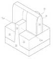
- the integrated circuit structureincludes substrate 20 , which may be a bulk silicon substrate.
- substrate 20may be doped with a p-type or an n-type impurity.
- Isolation regions, such as shallow trench isolation (STI) regions 22may be formed in substrate 20 .
- Fin 24is formed over top surfaces of STI regions 22 . Fin 24 may be formed by removing top portions of STI regions 22 , so that a portion of substrate 20 between neighboring STI regions 22 becomes a fin. Alternatively, fin 24 may be formed on top of substrate 20 by an epitaxial growth.
- STIshallow trench isolation
- substrate 20has a surface orientation of (100), and fin 24 extends along the ⁇ 110> direction. In other embodiments, substrate 20 may have other surface orientations such as (110), in which case fin 24 may extend in directions such as ⁇ 100>.
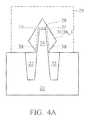
- Gate dielectric 26(not shown in FIG. 3 , please refer to FIG. 4A ), which may be formed of silicon oxide, high-k dielectric materials, or the like, is formed on the top surface and sidewalls of fin 24 .
- Gate electrode 28is formed on gate dielectric 26 .
- Gate spacers 32are formed on the sidewalls of gate electrode 28 .
- cross-sectional viewsare used to explain the concept of the embodiments. Unless specified otherwise, the cross-sectional views are obtained in vertical planes (referred to as source/drain planes hereinafter) crossing lines at the same position as line A-A in FIG. 3 . It is noted that line A-A crosses the (would-be) source/drain region, but not gate electrode 28 .
- epitaxy layer 36is deposited, for example, epitaxially grown on the exposed portion of fin 24 by selective epitaxial growth (SEG).
- Epitaxy layer 36(also referred to as epitaxy layer 36 _ 1 hereinafter) may be formed of a semiconductor material same as, or a semiconductor material different from, that of fin 24 .
- epitaxy layer 36 _ 1is formed of substantially pure silicon.
- epitaxy layer 36 _ 1may comprise silicon germanium (SiGe), silicon carbon (SiC), or the like.
- the formation methods of epitaxy layer 36 _ 1may include chemical vapor deposition (CVD), such as a reduced pressure CVD (RPCVD) or other applicable methods.
- CVDchemical vapor deposition
- RPCVDreduced pressure CVD
- the precursors for the epitaxymay include Si-containing gases and Ge-containing gases, such as SiH 4 and GeH 4 , and/or the like, and the partial pressures of the Si-containing gases and Ge-containing gases are adjusted to modify the atomic ratio of germanium to silicon.
- the resulting epitaxy layer 36 _ 1includes greater than about 20 atomic percent germanium.
- the germanium percentage in epitaxy layer 36 _ 1may also be between about 20 percent and about 50 atomic percent.
- FIG. 4Aalso illustrates gate dielectric 26 and gate electrode 28 . Since gate dielectric 26 and gate electrode 28 are not in the source/drain plane, they are illustrated using dotted lines. For simplicity, in subsequent drawings, gate dielectric 26 and gate electrode 28 are not illustrated.
- facetsmay be formed.
- the growth rate on surfaces having (111) surface orientations(referred to as (111) planes) is lower than that on other planes, such as (110) and (100) planes. Accordingly, facets 38 are formed as a result of the difference in the growth rates of different planes. If epitaxy layer 36 _ 1 is grown freely, eventually, facts 38 will have the (111) surface orientations (in other word, on (111) planes). In the beginning of the epitaxial growth of epitaxy layer 36 _ 1 , facets 38 may not be fully established. However, with the proceeding of the epitaxial growth, due to the difference in growth rates, facets 38 are gradually formed.
- etching gassuch as HCl gas
- HCl gasmay be added (as an etching gas) into the process gas, so that epitaxy layer 36 _ 1 is selectively grown on fin 24 , but not on STI regions 22 and gate spacers 32 (not shown in FIG. 4A , please refer to FIG. 3 ).
- no etching gasis added, or the amount of etching gas is small, so that there is a thin layer of epitaxy layer 36 _ 1 formed on STI regions 22 and gate spacers 32 , as shown in FIG. 4B . It is realized, however, that the portion of epitaxy layer 36 _ 1 on STI regions 22 and gate spacers 32 may not have a crystalline structure.
- the epitaxial growth of epitaxy layer 36 _ 1is stopped, and an etch step is performed, for example, by introducing etching gases such as HCl into the same chamber as the deposition of epitaxy layer 36 _ 1 .
- the epitaxial growth and the etch of epitaxy layer 36 _ 1are in-situ performed, that is, in a same process chamber with no vacuum break therebetween.
- the resulting structureis shown in FIG. 5 . It is observed that during the etch step, the corners of epitaxy layer 36 _ 1 are removed more than planar portions, and hence the surface profile of epitaxy layer 36 _ 1 is rounded.
- the resulting epitaxy layer 36 _ 1has an ellipse shape, with the outer surface of epitaxy layer 36 _ 1 having a profile close to an egg shape.
- the etch stepmay include, for example, introducing either HCl or the combination of HCl and GeH 4 into the process chamber.
- the wafer temperature during the etch stepmay be greater than about 500° C. with both HCl and GeH 4 being introduced, or greater than about 700° C. with HCl, but no GeH 4 , being introduced.
- plasmamay or may not be activated.
- deposition-etch cycleThe deposition step and the etch step as discussed in the preceding paragraphs in combination are referred to as a deposition-etch cycle.
- the formation of epitaxy layer 36includes only one deposition-etch cycle.
- a second deposition stepmay be performed, which may further be followed by a second etch step, wherein the second deposition step and the second etch step are referred to as the second deposition-etch cycle.
- FIGS. 6 and 7illustrate the structure resulted from the second deposition-etch cycle.
- epitaxy layer 36 _ 2is epitaxially grown on the remaining portion of epitaxy layer 36 _ 1 .
- epitaxy layers 36 _ 1 and 36 _ 2 in combinationare referred to as epitaxy layer 36 .
- Epitaxy layer 36 _ 2may be formed of the same material as epitaxy layer 36 _ 1 , although they may also be formed of different semiconductor materials. Accordingly, the interface between epitaxy layers 36 _ 1 and 36 _ 2 is illustrated using a dashed line since it may not be visible. More deposition-etch cycles may be repeated to further increase the depth of epitaxy layer 36 . The deposition-etch cycles may all be in-situ performed with no vacuum break therebetween.
- the thickness of epitaxy layer 36is increased over the preceding deposition-etch cycle, and the profile of the resulting epitaxy layer 36 may be more conformal then if epitaxy layer 36 is formed by a single epitaxy step.
- the profile of epitaxy layer 36may be more conformal.
- the throughputis lower.
- the thickness of the added portion of the epitaxy layeris denoted as T (refer to FIG. 6 ).
- T′the thickness of the added portion of epitaxy layer 36 is reduced to T′ (refer to FIG. 7 ).
- the ratio of T′/Treflects the percentage of epitaxy layer 36 removed in the etch step. In an embodiment, ratio T′/T is greater than about 50 percent, and may be between about 50 percent and about 95 percent.
- FIG. 8illustrates the subsequent formation of silicide region (which may also be a germano-silicide region) 54 .
- silicide region 54may be formed by blanket depositing a thin metal layer (not shown), such as nickel, platinum, palladium, vanadium, titanium, cobalt, tantalum, ytterbium, zirconium, and combinations thereof. The substrate is then heated, which causes silicon and germanium to react with the metal where contacted.
- a layer of metal silicide 54is formed between the remaining portion of epitaxy layer 36 and the metal layer.
- the un-reacted metal layeris selectively removed through the use of an etchant that attacks metal but does not attack the germano-silicide.
- FIG. 8illustrates the formation of a single-fin FinFET, wherein epitaxy layer 36 grown from one fin 24 does not merge with the epitaxy layer grown from other fins.
- FIG. 9illustrates that epitaxy layers 36 grown from neighboring fins 24 merge with each other to form a single epitaxy region. It is observed that due to the deposition-etch process, void 46 (if formed at all) caused by the merging of epitaxy layers 36 will be at least reduced, and possibly be eliminated. In addition, since defects are more likely to be generated from ⁇ 111> surface planes, by etching back epitaxy layer 36 , the sizes of the ⁇ 111> surface planes are reduced, resulting in the decrease in the defect density.
Landscapes
- Engineering & Computer Science (AREA)
- Physics & Mathematics (AREA)
- Condensed Matter Physics & Semiconductors (AREA)
- General Physics & Mathematics (AREA)
- Manufacturing & Machinery (AREA)
- Computer Hardware Design (AREA)
- Microelectronics & Electronic Packaging (AREA)
- Power Engineering (AREA)
- Insulated Gate Type Field-Effect Transistor (AREA)
Abstract
Description
- This application is a divisional of U.S. patent application Ser. No. 12/713,573, filed Feb. 26, 2010, and entitled “Epitaxy Profile Engineering for FinFETs,” which application is hereby incorporated herein by reference.
- This disclosure relates generally to semiconductor devices, and more particularly to structures and formation methods of semiconductor fins and fin field-effect transistors (FinFETs).
- With the increasing down scaling of integrated circuits and increasingly higher requirements for integrated circuits, transistors need to have higher drive currents with increasingly smaller dimensions. Fin field-effect transistors (FinFETs) were thus developed.
- Similar to planar transistors, source and drain silicides may be formed on the source and drain regions of FinFETs. However, since the fins of FinFETs are typically narrow, current crowding may occur. In addition, it is difficult to land contact plugs onto the source/drain portions of fins. Epitaxy semiconductor layers are thus formed on the fins to increase their volumes using epitaxy processes.
- The epitaxial processes, however, suffer from drawbacks.
FIG. 1 illustrates a cross-sectional view of a semiconductor structure including source/drain region2 (which is part of the original fin) andepitaxy layer 4 epitaxially grown on source/drain region 2. In contrast to conventional planar devices, the volumes of source/drain regions 2 are not confined by shallow trench isolation (STI)regions 6. Sinceepitaxy layer 4 may have a growth rate smaller on (111) planes than on other planes, the outer surface ofepitaxy layer 4 may not have a rectangular (or near-rectangular) profile as that of theoriginal fin 2. Instead,epitaxy layer 4 may extend laterally and formfacets 8. This may cause the excess reduction in the distance between epitaxy layers grown from neighboring fins. Accordingly, the merging window, in which the epitaxy layers growing from neighboring fins will not merge, is reduced. Further, even if the neighboringepitaxy layers 4 belong to a source/drain region of a same multi-fin FinFET,void 10 will be undesirably generated as a result of the merging ofepitaxy layers 4 grown from neighboringfins 2, as shown inFIG. 2 . - In accordance with one aspect of the embodiment, a method of forming an integrated circuit structure includes providing a wafer including a substrate and a semiconductor fin at a major surface of the substrate, and performing a deposition step to epitaxially grow an epitaxy layer on a top surface and sidewalls of the semiconductor fin, wherein the epitaxy layer includes a semiconductor material. An etch step is then performed to remove a portion of the epitaxy layer, with a remaining portion of the epitaxy layer remaining on the top surface and the sidewalls of the semiconductor fin.
- Other embodiments are also disclosed.
- For a more complete understanding of the embodiments, and the advantages thereof, reference is now made to the following descriptions taken in conjunction with the accompanying drawings, in which:
FIG. 1 illustrates a cross-sectional view of an epitaxy layer grown from a semiconductor fin;FIG. 2 illustrates the merging of the epitaxy layers grown from neighboring fins, wherein voids are generated when the epitaxy layers merge;FIGS. 3 through 8 are a perspective view and cross-sectional views of intermediate stages in the manufacturing of a FinFET in accordance with an embodiment; andFIG. 9 illustrates the merging of two epitaxy layers growing from neighboring semiconductor fins.- The making and using of the embodiments are discussed in detail below. It should be appreciated, however, that the embodiments provide many applicable inventive concepts that can be embodied in a wide variety of specific contexts.
- A novel fin field-effect transistor (FinFET) embodiment and the method of forming the same are presented. The intermediate stages of manufacturing the embodiment are illustrated. The variations of the embodiment are discussed. Throughout the various views and illustrative embodiments, like reference numbers are used to designate like elements.
- Referring to
FIG. 3 , an integrated circuit structure is formed. The integrated circuit structure includessubstrate 20, which may be a bulk silicon substrate.Substrate 20 may be doped with a p-type or an n-type impurity. Isolation regions, such as shallow trench isolation (STI)regions 22 may be formed insubstrate 20.Fin 24 is formed over top surfaces ofSTI regions 22.Fin 24 may be formed by removing top portions ofSTI regions 22, so that a portion ofsubstrate 20 between neighboringSTI regions 22 becomes a fin. Alternatively,fin 24 may be formed on top ofsubstrate 20 by an epitaxial growth. - In an embodiment,
substrate 20 has a surface orientation of (100), andfin 24 extends along the <110> direction. In other embodiments,substrate 20 may have other surface orientations such as (110), in whichcase fin 24 may extend in directions such as <100>. Gate dielectric26 (not shown inFIG. 3 , please refer toFIG. 4A ), which may be formed of silicon oxide, high-k dielectric materials, or the like, is formed on the top surface and sidewalls offin 24.Gate electrode 28 is formed on gate dielectric26.Gate spacers 32 are formed on the sidewalls ofgate electrode 28. - In the subsequent discussion, cross-sectional views are used to explain the concept of the embodiments. Unless specified otherwise, the cross-sectional views are obtained in vertical planes (referred to as source/drain planes hereinafter) crossing lines at the same position as line A-A in
FIG. 3 . It is noted that line A-A crosses the (would-be) source/drain region, but notgate electrode 28. - Next, as shown in
FIG. 4A ,epitaxy layer 36 is deposited, for example, epitaxially grown on the exposed portion offin 24 by selective epitaxial growth (SEG). Epitaxy layer36 (also referred to as epitaxy layer36_1 hereinafter) may be formed of a semiconductor material same as, or a semiconductor material different from, that offin 24. In an embodiment, epitaxy layer36_1 is formed of substantially pure silicon. In alternative embodiments, epitaxy layer36_1 may comprise silicon germanium (SiGe), silicon carbon (SiC), or the like. The formation methods of epitaxy layer36_1 may include chemical vapor deposition (CVD), such as a reduced pressure CVD (RPCVD) or other applicable methods. Depending on the desirable composition of epitaxy layer36_1, the precursors for the epitaxy may include Si-containing gases and Ge-containing gases, such as SiH4and GeH4, and/or the like, and the partial pressures of the Si-containing gases and Ge-containing gases are adjusted to modify the atomic ratio of germanium to silicon. In an embodiment in which SiGe is desirable for forming epitaxy layer36_1, the resulting epitaxy layer36_1 includes greater than about20 atomic percent germanium. The germanium percentage in epitaxy layer36_1 may also be between about20 percent and about50 atomic percent. FIG. 4A also illustrates gate dielectric26 andgate electrode 28. Since gate dielectric26 andgate electrode 28 are not in the source/drain plane, they are illustrated using dotted lines. For simplicity, in subsequent drawings, gate dielectric26 andgate electrode 28 are not illustrated.- It is observed that due to different growth rates on different surface planes, facets may be formed. For example, the growth rate on surfaces having (111) surface orientations (referred to as (111) planes) is lower than that on other planes, such as (110) and (100) planes. Accordingly,
facets 38 are formed as a result of the difference in the growth rates of different planes. If epitaxy layer36_1 is grown freely, eventually,facts 38 will have the (111) surface orientations (in other word, on (111) planes). In the beginning of the epitaxial growth of epitaxy layer36_1,facets 38 may not be fully established. However, with the proceeding of the epitaxial growth, due to the difference in growth rates,facets 38 are gradually formed. - During the epitaxy process, etching gas, such as HCl gas, may be added (as an etching gas) into the process gas, so that epitaxy layer36_1 is selectively grown on
fin 24, but not onSTI regions 22 and gate spacers32 (not shown inFIG. 4A , please refer toFIG. 3 ). In alternative embodiments, no etching gas is added, or the amount of etching gas is small, so that there is a thin layer of epitaxy layer36_1 formed onSTI regions 22 andgate spacers 32, as shown inFIG. 4B . It is realized, however, that the portion of epitaxy layer36_1 onSTI regions 22 andgate spacers 32 may not have a crystalline structure. - Referring to
FIG. 5 , after the formation of epitaxy layer36_1, the epitaxial growth of epitaxy layer36_1 is stopped, and an etch step is performed, for example, by introducing etching gases such as HCl into the same chamber as the deposition of epitaxy layer36_1. In an embodiment, the epitaxial growth and the etch of epitaxy layer36_1 are in-situ performed, that is, in a same process chamber with no vacuum break therebetween. The resulting structure is shown inFIG. 5 . It is observed that during the etch step, the corners of epitaxy layer36_1 are removed more than planar portions, and hence the surface profile of epitaxy layer36_1 is rounded. In an exemplary embodiment, after the etch step, the resulting epitaxy layer36_1 has an ellipse shape, with the outer surface of epitaxy layer36_1 having a profile close to an egg shape. The etch step may include, for example, introducing either HCl or the combination of HCl and GeH4into the process chamber. The wafer temperature during the etch step may be greater than about 500° C. with both HCl and GeH4being introduced, or greater than about 700° C. with HCl, but no GeH4, being introduced. During the etch step, plasma may or may not be activated. - The deposition step and the etch step as discussed in the preceding paragraphs in combination are referred to as a deposition-etch cycle. In an embodiment, the formation of
epitaxy layer 36 includes only one deposition-etch cycle. In alternative embodiments, after the first deposition-etch cycle, a second deposition step may be performed, which may further be followed by a second etch step, wherein the second deposition step and the second etch step are referred to as the second deposition-etch cycle.FIGS. 6 and 7 illustrate the structure resulted from the second deposition-etch cycle. InFIG. 6 , epitaxy layer36_2 is epitaxially grown on the remaining portion of epitaxy layer36_1. Throughout the description, epitaxy layers36_1 and36_2 in combination are referred to asepitaxy layer 36. Epitaxy layer36_2 may be formed of the same material as epitaxy layer36_1, although they may also be formed of different semiconductor materials. Accordingly, the interface between epitaxy layers36_1 and36_2 is illustrated using a dashed line since it may not be visible. More deposition-etch cycles may be repeated to further increase the depth ofepitaxy layer 36. The deposition-etch cycles may all be in-situ performed with no vacuum break therebetween. For each of the additional deposition-etch cycles, the thickness ofepitaxy layer 36 is increased over the preceding deposition-etch cycle, and the profile of the resultingepitaxy layer 36 may be more conformal then ifepitaxy layer 36 is formed by a single epitaxy step. Advantageously, by dividing one deposition-etch cycle into a plurality of deposition-etch cycles, the profile ofepitaxy layer 36 may be more conformal. - With more portions of
epitaxy layer 36 being etched,epitaxy layer 36 is more conformal. However, with a higher degree of etch back, the throughput is lower. In an embodiment, in the deposition step in each of the deposition-etch cycles, the thickness of the added portion of the epitaxy layer is denoted as T (refer toFIG. 6 ). After the etch step, the thickness of the added portion ofepitaxy layer 36 is reduced to T′ (refer toFIG. 7 ). The ratio of T′/T reflects the percentage ofepitaxy layer 36 removed in the etch step. In an embodiment, ratio T′/T is greater than about 50 percent, and may be between about 50 percent and about 95 percent. - After the formation of
epitaxy layer 36, a source/drain implantation is performed, so thatepitaxy layer 36 becomes part of the source/drain region of the resultingFinFET 60.FIG. 8 illustrates the subsequent formation of silicide region (which may also be a germano-silicide region)54. As is known in the art, silicide region54 may be formed by blanket depositing a thin metal layer (not shown), such as nickel, platinum, palladium, vanadium, titanium, cobalt, tantalum, ytterbium, zirconium, and combinations thereof. The substrate is then heated, which causes silicon and germanium to react with the metal where contacted. After the reaction, a layer of metal silicide54 is formed between the remaining portion ofepitaxy layer 36 and the metal layer. The un-reacted metal layer is selectively removed through the use of an etchant that attacks metal but does not attack the germano-silicide. FIG. 8 illustrates the formation of a single-fin FinFET, whereinepitaxy layer 36 grown from onefin 24 does not merge with the epitaxy layer grown from other fins.FIG. 9 illustrates that epitaxy layers36 grown from neighboringfins 24 merge with each other to form a single epitaxy region. It is observed that due to the deposition-etch process, void46 (if formed at all) caused by the merging of epitaxy layers36 will be at least reduced, and possibly be eliminated. In addition, since defects are more likely to be generated from <111> surface planes, by etching backepitaxy layer 36, the sizes of the <111> surface planes are reduced, resulting in the decrease in the defect density.- Although the embodiments and their advantages have been described in detail, it should be understood that various changes, substitutions, and alterations can be made herein without departing from the spirit and scope of the disclosure as defined by the appended claims. Moreover, the scope of the present application is not intended to be limited to the particular embodiments of the process, machine, manufacture, and composition of matter, means, methods and steps described in the specification. As one of ordinary skill in the art will readily appreciate from the disclosure, processes, machines, manufacture, compositions of matter, means, methods, or steps, presently existing or later to be developed, that perform substantially the same function or achieve substantially the same result as the corresponding embodiments described herein may be utilized according to the disclosure. Accordingly, the appended claims are intended to include within their scope such processes, machines, manufacture, compositions of matter, means, methods, or steps. In addition, each claim constitutes a separate embodiment, and the combination of various claims and embodiments are within the scope of the invention.
Claims (3)
1. An integrated circuit structure comprising:
insulation regions comprising top surfaces; and
a fin field-effect transistor (FinFET) comprising:
a semiconductor fin over and adjacent to the insulation regions;
a gate dielectric on a top surface, and extending on sidewalls, of the semiconductor fin;
a gate electrode on the gate dielectric; and
a source/drain region over the insulation regions and adjoining the semiconductor fin, wherein the source/drain region comprises:
an extension of the semiconductor fin; and
an epitaxy layer on a top surface and sidewalls of the extension of the semiconductor fin, wherein an outer surface of the epitaxy layer has an ellipse profile.
2. The integrated circuit structure ofclaim 1 , wherein the epitaxy layer and the extension of the semiconductor fin are formed of a same semiconductor material.
3. The integrated circuit structure ofclaim 1 , wherein the epitaxy layer and the extension of the semiconductor fin are formed of different semiconductor materials.
Priority Applications (1)
| Application Number | Priority Date | Filing Date | Title |
|---|---|---|---|
| US13/608,961US9666691B2 (en) | 2010-02-26 | 2012-09-10 | Epitaxy profile engineering for FinFETs |
Applications Claiming Priority (2)
| Application Number | Priority Date | Filing Date | Title |
|---|---|---|---|
| US12/713,573US8263451B2 (en) | 2010-02-26 | 2010-02-26 | Epitaxy profile engineering for FinFETs |
| US13/608,961US9666691B2 (en) | 2010-02-26 | 2012-09-10 | Epitaxy profile engineering for FinFETs |
Related Parent Applications (1)
| Application Number | Title | Priority Date | Filing Date |
|---|---|---|---|
| US12/713,573DivisionUS8263451B2 (en) | 2010-02-26 | 2010-02-26 | Epitaxy profile engineering for FinFETs |
Publications (2)
| Publication Number | Publication Date |
|---|---|
| US20130001705A1true US20130001705A1 (en) | 2013-01-03 |
| US9666691B2 US9666691B2 (en) | 2017-05-30 |
Family
ID=44490950
Family Applications (2)
| Application Number | Title | Priority Date | Filing Date |
|---|---|---|---|
| US12/713,573Active2030-07-17US8263451B2 (en) | 2010-02-26 | 2010-02-26 | Epitaxy profile engineering for FinFETs |
| US13/608,961Active2030-10-25US9666691B2 (en) | 2010-02-26 | 2012-09-10 | Epitaxy profile engineering for FinFETs |
Family Applications Before (1)
| Application Number | Title | Priority Date | Filing Date |
|---|---|---|---|
| US12/713,573Active2030-07-17US8263451B2 (en) | 2010-02-26 | 2010-02-26 | Epitaxy profile engineering for FinFETs |
Country Status (4)
| Country | Link |
|---|---|
| US (2) | US8263451B2 (en) |
| KR (1) | KR101153154B1 (en) |
| CN (1) | CN102169853B (en) |
| TW (1) | TWI420573B (en) |
Cited By (16)
| Publication number | Priority date | Publication date | Assignee | Title |
|---|---|---|---|---|
| US20140203370A1 (en)* | 2013-01-24 | 2014-07-24 | Shigenobu Maeda | Semiconductor Device and Fabricating Method Thereof |
| US8815661B1 (en)* | 2013-02-15 | 2014-08-26 | International Business Machines Corporation | MIM capacitor in FinFET structure |
| US8993406B1 (en) | 2013-09-10 | 2015-03-31 | International Business Machines Corporation | FinFET device having a merged source drain region under contact areas and unmerged fins between contact areas, and a method of manufacturing same |
| US9054218B2 (en) | 2013-08-07 | 2015-06-09 | International Business Machines Corporation | Method of manufacturing a FinFET device using a sacrificial epitaxy region for improved fin merge and FinFET device formed by same |
| US9087900B1 (en) | 2014-01-07 | 2015-07-21 | Samsung Electronics Co., Ltd. | Semiconductor device and method for fabricating the same |
| WO2015147842A1 (en)* | 2014-03-27 | 2015-10-01 | Intel Corporation | Confined epitaxial regions for semiconductor devices and methods of fabricating semiconductor devices having confined epitaxial regions |
| US20160003082A1 (en)* | 2013-02-28 | 2016-01-07 | United Technologies Corporation | Contoured blade outer air seal for a gas turbine engine |
| US9431534B2 (en) | 2014-12-02 | 2016-08-30 | Globalfoundries Inc. | Asymmetric field effect transistor cap layer |
| US20160318191A1 (en)* | 2013-12-10 | 2016-11-03 | Kawasaki Jukogyo Kabushiki Kaisha | Workpiece reverse support device and robot cell including the same device |
| US20180069131A1 (en)* | 2016-09-02 | 2018-03-08 | International Business Machines Corporation | Stacked series connected vfets for high voltage applications |
| TWI641031B (en)* | 2017-07-31 | 2018-11-11 | 台灣積體電路製造股份有限公司 | Method for manufacturing fin field effect transistor |
| US10367077B1 (en) | 2018-04-27 | 2019-07-30 | International Business Machines Corporation | Wrap around contact using sacrificial mandrel |
| US10438855B2 (en) | 2017-02-17 | 2019-10-08 | International Business Machines Corporation | Dual channel FinFETs having uniform fin heights |
| US10593775B2 (en) | 2016-11-29 | 2020-03-17 | Taiwan Semiconductor Manufacturing Co., Ltd. | Semiconductor device and manufacturing method thereof |
| DE112013005528B4 (en) | 2012-12-19 | 2024-11-07 | Intel Corporation | Group III-N transistors on nanoscale template structures |
| DE102017128062B4 (en) | 2017-06-16 | 2025-09-04 | Taiwan Semiconductor Manufacturing Co. Ltd. | Source and drain epitaxy redesign |
Families Citing this family (118)
| Publication number | Priority date | Publication date | Assignee | Title |
|---|---|---|---|---|
| US8399931B2 (en)* | 2010-06-30 | 2013-03-19 | Taiwan Semiconductor Manufacturing Company, Ltd. | Layout for multiple-fin SRAM cell |
| US9263339B2 (en)* | 2010-05-20 | 2016-02-16 | Taiwan Semiconductor Manufacturing Company, Ltd. | Selective etching in the formation of epitaxy regions in MOS devices |
| US8753942B2 (en)* | 2010-12-01 | 2014-06-17 | Intel Corporation | Silicon and silicon germanium nanowire structures |
| JP2013115272A (en)* | 2011-11-29 | 2013-06-10 | Toshiba Corp | Semiconductor device and method of manufacturing the same |
| US8609499B2 (en)* | 2012-01-09 | 2013-12-17 | Taiwan Semiconductor Manufacturing Company, Ltd. | FinFETs and the methods for forming the same |
| US8759184B2 (en) | 2012-01-09 | 2014-06-24 | Taiwan Semiconductor Manufacturing Company, Ltd. | FinFETs and the methods for forming the same |
| US9466696B2 (en) | 2012-01-24 | 2016-10-11 | Taiwan Semiconductor Manufacturing Company, Ltd. | FinFETs and methods for forming the same |
| US9171925B2 (en) | 2012-01-24 | 2015-10-27 | Taiwan Semiconductor Manufacturing Company, Ltd. | Multi-gate devices with replaced-channels and methods for forming the same |
| US9281378B2 (en) | 2012-01-24 | 2016-03-08 | Taiwan Semiconductor Manufacturing Company, Ltd. | Fin recess last process for FinFET fabrication |
| US8659032B2 (en)* | 2012-01-31 | 2014-02-25 | Taiwan Semiconductor Manufacturing Company, Ltd. | FinFET and method of fabricating the same |
| US20130200483A1 (en)* | 2012-02-08 | 2013-08-08 | United Microelectronics Corp. | Fin structure and method of forming the same |
| KR101835655B1 (en)* | 2012-03-06 | 2018-03-07 | 삼성전자주식회사 | FinFET and method of fabricating the same |
| US9012286B2 (en)* | 2012-04-12 | 2015-04-21 | Globalfoundries Inc. | Methods of forming FinFET semiconductor devices so as to tune the threshold voltage of such devices |
| US9368388B2 (en)* | 2012-04-13 | 2016-06-14 | Taiwan Semiconductor Manufacturing Company, Ltd. | Apparatus for FinFETs |
| US8580642B1 (en) | 2012-05-21 | 2013-11-12 | Globalfoundries Inc. | Methods of forming FinFET devices with alternative channel materials |
| US8673718B2 (en) | 2012-07-09 | 2014-03-18 | Globalfoundries Inc. | Methods of forming FinFET devices with alternative channel materials |
| US8703556B2 (en) | 2012-08-30 | 2014-04-22 | Taiwan Semiconductor Manufacturing Company, Ltd. | Method of making a FinFET device |
| US8723225B2 (en)* | 2012-10-04 | 2014-05-13 | Taiwan Semiconductor Manufacturing Company, Ltd. | Guard rings on fin structures |
| TWI573270B (en)* | 2012-10-29 | 2017-03-01 | 聯華電子股份有限公司 | Multigate field effect transistor and process thereof |
| US9349837B2 (en) | 2012-11-09 | 2016-05-24 | Taiwan Semiconductor Manufacturing Company, Ltd. | Recessing STI to increase Fin height in Fin-first process |
| US8866235B2 (en)* | 2012-11-09 | 2014-10-21 | Taiwan Semiconductor Manufacturing Company, Ltd. | Source and drain dislocation fabrication in FinFETs |
| US9443962B2 (en) | 2012-11-09 | 2016-09-13 | Taiwan Semiconductor Manufacturing Company, Ltd. | Recessing STI to increase fin height in fin-first process |
| US8946029B2 (en)* | 2012-11-12 | 2015-02-03 | GlobalFoundries, Inc. | Methods of manufacturing integrated circuits having FinFET structures with epitaxially formed source/drain regions |
| US9029835B2 (en)* | 2012-12-20 | 2015-05-12 | Intel Corporation | Epitaxial film on nanoscale structure |
| US9397217B2 (en) | 2012-12-28 | 2016-07-19 | Taiwan Semiconductor Manufacturing Company, Ltd. | Contact structure of non-planar semiconductor device |
| CN103928328B (en)* | 2013-01-10 | 2016-12-28 | 中芯国际集成电路制造(上海)有限公司 | The forming method of fin formula field effect transistor |
| US9859429B2 (en) | 2013-01-14 | 2018-01-02 | Taiwan Semiconductor Manufacturing Company, Ltd. | FinFET device and method of fabricating same |
| US8921191B2 (en)* | 2013-02-05 | 2014-12-30 | GlobalFoundries, Inc. | Integrated circuits including FINFET devices with lower contact resistance and reduced parasitic capacitance and methods for fabricating the same |
| US9831345B2 (en) | 2013-03-11 | 2017-11-28 | Taiwan Semiconductor Manufacturing Company, Ltd. | FinFET with rounded source/drain profile |
| US8796093B1 (en)* | 2013-03-14 | 2014-08-05 | International Business Machines Corporation | Doping of FinFET structures |
| US8921940B2 (en) | 2013-03-15 | 2014-12-30 | Samsung Electronics Co., Ltd. | Semiconductor device and a method for fabricating the same |
| US8859379B2 (en) | 2013-03-15 | 2014-10-14 | International Business Machines Corporation | Stress enhanced finFET devices |
| US9752251B2 (en)* | 2013-04-15 | 2017-09-05 | International Business Machines Corporation | Self-limiting selective epitaxy process for preventing merger of semiconductor fins |
| US9257536B2 (en) | 2013-04-22 | 2016-02-09 | Globalfoundries Inc. | FinFET with crystalline insulator |
| US9953975B2 (en) | 2013-07-19 | 2018-04-24 | Taiwan Semiconductor Manufacturing Company, Ltd. | Methods for forming STI regions in integrated circuits |
| KR102068980B1 (en) | 2013-08-01 | 2020-01-22 | 삼성전자 주식회사 | Semiconductor device and method for fabricating the same |
| US9520502B2 (en) | 2013-10-15 | 2016-12-13 | Taiwan Semiconductor Manufacturing Company, Ltd. | FinFETs having epitaxial capping layer on fin and methods for forming the same |
| US9257537B2 (en)* | 2013-12-27 | 2016-02-09 | International Business Machines Corporation | Finfet including improved epitaxial topology |
| US9054189B1 (en) | 2014-01-06 | 2015-06-09 | Samsung Electronics Co., Ltd. | Semiconductor device and method for fabricating the same |
| KR102155181B1 (en) | 2014-01-28 | 2020-09-11 | 삼성전자주식회사 | Semiconductor devices and methods of manufacturing the same |
| WO2015147866A1 (en)* | 2014-03-28 | 2015-10-01 | Intel Corporation | Selectively regrown top contact for vertical semiconductor devices |
| KR102017611B1 (en) | 2014-04-04 | 2019-09-04 | 삼성전자주식회사 | Semiconductor device and method of manufacturing the same |
| US9443769B2 (en) | 2014-04-21 | 2016-09-13 | Taiwan Semiconductor Manufacturing Company, Ltd. | Wrap-around contact |
| KR102146469B1 (en)* | 2014-04-30 | 2020-08-21 | 삼성전자 주식회사 | Semiconductor device and method for fabricating the same |
| KR102158961B1 (en) | 2014-05-13 | 2020-09-24 | 삼성전자 주식회사 | Semiconductor device and method for fabricating the same |
| KR102200345B1 (en) | 2014-06-26 | 2021-01-11 | 삼성전자주식회사 | Semiconductor device and method of manufacturing the same |
| CN105336569B (en)* | 2014-07-10 | 2019-01-18 | 中国科学院微电子研究所 | Semiconductor device manufacturing method |
| KR102269228B1 (en)* | 2014-07-31 | 2021-06-25 | 삼성전자주식회사 | Methods of manufacturing semiconductor devices |
| US9455323B2 (en) | 2014-08-28 | 2016-09-27 | International Business Machines Corporation | Under-spacer doping in fin-based semiconductor devices |
| US9385197B2 (en) | 2014-08-29 | 2016-07-05 | Taiwan Semiconductor Manufacturing Co., Ltd | Semiconductor structure with contact over source/drain structure and method for forming the same |
| KR102410135B1 (en)* | 2014-09-12 | 2022-06-17 | 삼성전자주식회사 | Semiconductor device and method for fabricating the same |
| KR102230198B1 (en) | 2014-09-23 | 2021-03-19 | 삼성전자주식회사 | Semiconductor device and method for manufacturing the same |
| US9299706B1 (en)* | 2014-09-25 | 2016-03-29 | International Business Machines Corporation | Single source/drain epitaxy for co-integrating nFET semiconductor fins and pFET semiconductor fins |
| CN105529241A (en)* | 2014-09-29 | 2016-04-27 | 中芯国际集成电路制造(上海)有限公司 | Semiconductor structure and formation method thereof |
| US9324820B1 (en)* | 2014-10-28 | 2016-04-26 | Taiwan Semiconductor Manufacturing Co., Ltd | Method for forming semiconductor structure with metallic layer over source/drain structure |
| CN107112213B (en) | 2014-10-30 | 2021-04-16 | 应用材料公司 | Method for growing thin epitaxial films at low temperature |
| US9362405B1 (en)* | 2014-12-04 | 2016-06-07 | Globalfoundries Inc. | Channel cladding last process flow for forming a channel region on a FinFET device |
| US9269628B1 (en) | 2014-12-04 | 2016-02-23 | Globalfoundries Inc. | Methods of removing portions of at least one fin structure so as to form isolation regions when forming FinFET semiconductor devices |
| KR20160072476A (en)* | 2014-12-15 | 2016-06-23 | 삼성전자주식회사 | Semiconductor device and method of fabricating the same |
| US9577099B2 (en)* | 2015-03-09 | 2017-02-21 | Globalfoundries Inc. | Diamond shaped source drain epitaxy with underlying buffer layer |
| KR102407994B1 (en)* | 2015-03-23 | 2022-06-14 | 삼성전자주식회사 | Semiconductor device and method for manufacturing the same |
| KR102351659B1 (en) | 2015-04-03 | 2022-01-17 | 삼성전자주식회사 | Semiconductor devices including field effect transistors |
| KR102251060B1 (en) | 2015-04-06 | 2021-05-14 | 삼성전자주식회사 | Semiconductor devices and methods of manufacturing semiconductor devices |
| US9768261B2 (en)* | 2015-04-17 | 2017-09-19 | Taiwan Semiconductor Manufacturing Company Ltd. | Semiconductor structure and method of forming the same |
| KR102310076B1 (en) | 2015-04-23 | 2021-10-08 | 삼성전자주식회사 | Semiconductor devices having a source/drain ofasymmetrical shape |
| US10032910B2 (en)* | 2015-04-24 | 2018-07-24 | GlobalFoundries, Inc. | FinFET devices having asymmetrical epitaxially-grown source and drain regions and methods of forming the same |
| KR102310082B1 (en) | 2015-04-27 | 2021-10-08 | 삼성전자주식회사 | Semiconductor device having a fin body and an epitaxial layer |
| KR102392695B1 (en)* | 2015-05-26 | 2022-05-02 | 삼성전자주식회사 | A semiconductor device and a method of fabricating the same |
| US9379025B1 (en) | 2015-06-19 | 2016-06-28 | International Business Machines Corporation | Method of forming source/drain contacts in unmerged FinFETs |
| US9680020B2 (en)* | 2015-07-09 | 2017-06-13 | Globalfoundries Inc. | Increased contact area for FinFETs |
| US9666581B2 (en)* | 2015-08-21 | 2017-05-30 | Taiwan Semiconductor Manufacturing Company, Ltd. | FinFET with source/drain structure and method of fabrication thereof |
| US10164097B2 (en)* | 2015-09-11 | 2018-12-25 | Taiwan Semiconductor Manufacturing Co., Ltd. | Semiconductor device and manufacturing method thereof |
| DE102016102679B4 (en) | 2015-09-15 | 2024-09-12 | Taiwan Semiconductor Manufacturing Co., Ltd. | FETS AND METHODS OF FORMING FETS |
| US9905641B2 (en) | 2015-09-15 | 2018-02-27 | Taiwan Semiconductor Manufacturing Company, Ltd. | Semiconductor device and manufacturing method thereof |
| US9831116B2 (en) | 2015-09-15 | 2017-11-28 | Taiwan Semiconductor Manufacturing Company, Ltd. | FETS and methods of forming FETs |
| US10177143B2 (en) | 2015-10-28 | 2019-01-08 | Taiwan Semiconductor Manufacturing Company Limited | FinFET device and method for fabricating the same |
| KR102262830B1 (en)* | 2015-11-03 | 2021-06-08 | 삼성전자주식회사 | Semiconductor device |
| US20170140992A1 (en)* | 2015-11-16 | 2017-05-18 | Taiwan Semiconductor Manufacturing Co., Ltd. | Fin field effect transistor and method for fabricating the same |
| US9735274B2 (en)* | 2015-11-20 | 2017-08-15 | Taiwan Semiconductor Manufacturing Co., Ltd. | Semiconductor device including a stacked wire structure |
| US10497701B2 (en)* | 2015-12-16 | 2019-12-03 | Taiwan Semiconductor Manufacturing Co., Ltd. | Semiconductor device and manufacturing method thereof |
| US9496400B1 (en) | 2015-12-29 | 2016-11-15 | International Business Machines Corporation | FinFET with stacked faceted S/D epitaxy for improved contact resistance |
| CN107026084B (en)* | 2016-02-02 | 2020-03-31 | 中芯国际集成电路制造(上海)有限公司 | Semiconductor device and method for manufacturing the same |
| US9536989B1 (en) | 2016-02-15 | 2017-01-03 | Globalfoundries Inc. | Field-effect transistors with source/drain regions of reduced topography |
| US9865504B2 (en) | 2016-03-04 | 2018-01-09 | Taiwan Semiconductor Manufacturing Company, Ltd. | Semiconductor device and manufacturing method thereof |
| US10002867B2 (en)* | 2016-03-07 | 2018-06-19 | Taiwan Semiconductor Manufacturing Co., Ltd. | Fin-type field effect transistor structure and manufacturing method thereof |
| CN107516636A (en)* | 2016-06-17 | 2017-12-26 | 上海新昇半导体科技有限公司 | A low temperature epitaxy method and device |
| US10164098B2 (en) | 2016-06-30 | 2018-12-25 | Taiwan Semiconductor Manufacturing Company, Ltd. | Method of manufacturing semiconductor device |
| US10205002B2 (en) | 2016-07-26 | 2019-02-12 | Applied Materials, Inc. | Method of epitaxial growth shape control for CMOS applications |
| US10453943B2 (en)* | 2016-11-29 | 2019-10-22 | Taiwan Semiconductor Manufacturing Company, Ltd. | FETS and methods of forming FETS |
| US9953875B1 (en)* | 2016-11-30 | 2018-04-24 | Taiwan Semiconductor Manufacturing Company | Contact resistance control in epitaxial structures of finFET |
| US9865595B1 (en) | 2016-12-14 | 2018-01-09 | Taiwan Semiconductor Manufacturing Co., Ltd. | FinFET device with epitaxial structures that wrap around the fins and the method of fabricating the same |
| DE102017117970B4 (en) | 2016-12-15 | 2022-08-25 | Taiwan Semiconductor Manufacturing Co., Ltd. | Semiconductor device having fused epitaxial features with an arch-like underside and method of making same |
| DE102017126881B4 (en)* | 2016-12-15 | 2024-04-25 | Taiwan Semiconductor Manufacturing Co., Ltd. | FinFET structures and methods for their formation |
| US10147609B2 (en) | 2016-12-15 | 2018-12-04 | Taiwan Semiconductor Manufacturing Co., Ltd. | Semiconductor epitaxy bordering isolation structure |
| DE102017111540B4 (en) | 2016-12-15 | 2024-09-05 | Taiwan Semiconductor Manufacturing Co., Ltd. | SOURCE AND DRAIN PRODUCTION PROCESS FOR FIN FIELD EFFECT TRANSISTORS |
| US10049936B2 (en) | 2016-12-15 | 2018-08-14 | Taiwan Semiconductor Manufacturing Co., Ltd. | Semiconductor device having merged epitaxial features with Arc-like bottom surface and method of making the same |
| US10510762B2 (en) | 2016-12-15 | 2019-12-17 | Taiwan Semiconductor Manufacturing Co., Ltd. | Source and drain formation technique for fin-like field effect transistor |
| US11476349B2 (en)* | 2016-12-15 | 2022-10-18 | Taiwan Semiconductor Manufacturing Company, Ltd. | FinFET structures and methods of forming the same |
| US10551749B2 (en) | 2017-01-04 | 2020-02-04 | Kla-Tencor Corporation | Metrology targets with supplementary structures in an intermediate layer |
| KR102414182B1 (en) | 2017-06-29 | 2022-06-28 | 삼성전자주식회사 | Semiconductor device |
| US10516037B2 (en) | 2017-06-30 | 2019-12-24 | Taiwan Semiconductor Manufacturing Co., Ltd. | Method of forming shaped source/drain epitaxial layers of a semiconductor device |
| US10510875B2 (en)* | 2017-07-31 | 2019-12-17 | Taiwan Semiconductor Manufacturing Co., Ltd. | Source and drain structure with reduced contact resistance and enhanced mobility |
| KR102365109B1 (en) | 2017-08-22 | 2022-02-18 | 삼성전자주식회사 | Integrated circuit devices |
| US10141231B1 (en)* | 2017-08-28 | 2018-11-27 | Taiwan Semiconductor Manufacturing Co., Ltd. | FinFET device with wrapped-around epitaxial structure and manufacturing method thereof |
| DE102017125352B4 (en)* | 2017-08-30 | 2020-07-09 | Taiwan Semiconductor Manufacturing Co., Ltd. | Process for forming FinFETs |
| US10868181B2 (en)* | 2017-09-27 | 2020-12-15 | Taiwan Semiconductor Manufacturing Co., Ltd. | Semiconductor structure with blocking layer and method for forming the same |
| US10680084B2 (en) | 2017-11-10 | 2020-06-09 | Taiwan Semiconductor Manufacturing Co., Ltd. | Epitaxial structures for fin-like field effect transistors |
| CN109920735A (en)* | 2017-12-12 | 2019-06-21 | 中芯国际集成电路制造(上海)有限公司 | Semiconductor structure and forming method thereof |
| KR102612196B1 (en) | 2018-06-20 | 2023-12-12 | 삼성전자주식회사 | Semiconductor devices |
| KR102456669B1 (en) | 2018-07-16 | 2022-10-20 | 삼성전자주식회사 | Semiconductor device |
| JP6612937B2 (en)* | 2018-07-18 | 2019-11-27 | ルネサスエレクトロニクス株式会社 | Semiconductor device |
| US11222951B2 (en) | 2018-08-31 | 2022-01-11 | Taiwan Semiconductor Manufacturing Co., Ltd. | Epitaxial source/drain structure and method |
| DE102019118613B4 (en) | 2018-11-29 | 2024-12-05 | Taiwan Semiconductor Manufacturing Company, Ltd. | CONFINED SOURCE/DRAIN EPITAXY AREAS AND METHODS FOR THEIR PRODUCTION |
| US11101347B2 (en)* | 2018-11-29 | 2021-08-24 | Taiwan Semiconductor Manufacturing Company, Ltd. | Confined source/drain epitaxy regions and method forming same |
| EP3900053A4 (en)* | 2018-12-19 | 2022-09-28 | National Research Council of Canada | METHOD OF MANUFACTURING AN AVALANCHE PHOTODIODE WITH SINGLE DIFFUSION |
| US11088150B2 (en) | 2019-01-28 | 2021-08-10 | Taiwan Semiconductor Manufacturing Co., Ltd. | Semiconductor device and manufacturing method thereof |
| KR102608830B1 (en)* | 2019-06-12 | 2023-11-30 | 어플라이드 머티어리얼스, 인코포레이티드 | Optional Methods for Manufacturing Devices and Structures |
| US11600728B2 (en)* | 2020-06-15 | 2023-03-07 | Taiwan Semiconductor Manufacturing Co., Ltd. | Method of manufacturing a facet-free source/drain epitaxial structure having an amorphous or polycrystalline layer |
Citations (5)
| Publication number | Priority date | Publication date | Assignee | Title |
|---|---|---|---|---|
| US6858478B2 (en)* | 2002-08-23 | 2005-02-22 | Intel Corporation | Tri-gate devices and methods of fabrication |
| US20060046388A1 (en)* | 2004-08-27 | 2006-03-02 | Samsung Electronics Co., Ltd. | Nonvolatile semiconductor device and method of fabricating the same |
| US20080003755A1 (en)* | 2006-06-30 | 2008-01-03 | Uday Shah | Sacrificial oxide layer which enables spacer over-etch in tri-gate architectures |
| US20090026505A1 (en)* | 2007-07-27 | 2009-01-29 | Kabushiki Kaisha Toshiba | Semiconductor device and method of fabricating the same |
| US20090085027A1 (en)* | 2007-09-29 | 2009-04-02 | Intel Corporation | Three dimensional strained quantum wells and three dimensional strained surface channels by ge confinement method |
Family Cites Families (26)
| Publication number | Priority date | Publication date | Assignee | Title |
|---|---|---|---|---|
| JP3782021B2 (en)* | 2002-02-22 | 2006-06-07 | 株式会社東芝 | Semiconductor device, semiconductor device manufacturing method, and semiconductor substrate manufacturing method |
| US6706571B1 (en)* | 2002-10-22 | 2004-03-16 | Advanced Micro Devices, Inc. | Method for forming multiple structures in a semiconductor device |
| US7259425B2 (en)* | 2003-01-23 | 2007-08-21 | Advanced Micro Devices, Inc. | Tri-gate and gate around MOSFET devices and methods for making same |
| US7148526B1 (en)* | 2003-01-23 | 2006-12-12 | Advanced Micro Devices, Inc. | Germanium MOSFET devices and methods for making same |
| JP4865331B2 (en)* | 2003-10-20 | 2012-02-01 | ルネサスエレクトロニクス株式会社 | Semiconductor device and manufacturing method of semiconductor device |
| KR100513405B1 (en)* | 2003-12-16 | 2005-09-09 | 삼성전자주식회사 | Method for forming fin field effect transistor |
| US7300837B2 (en)* | 2004-04-30 | 2007-11-27 | Taiwan Semiconductor Manufacturing Co., Ltd | FinFET transistor device on SOI and method of fabrication |
| US7547605B2 (en)* | 2004-11-22 | 2009-06-16 | Taiwan Semiconductor Manufacturing Company | Microelectronic device and a method for its manufacture |
| US7807523B2 (en)* | 2005-07-01 | 2010-10-05 | Synopsys, Inc. | Sequential selective epitaxial growth |
| US8466490B2 (en)* | 2005-07-01 | 2013-06-18 | Synopsys, Inc. | Enhanced segmented channel MOS transistor with multi layer regions |
| US7508031B2 (en)* | 2005-07-01 | 2009-03-24 | Synopsys, Inc. | Enhanced segmented channel MOS transistor with narrowed base regions |
| US7247887B2 (en)* | 2005-07-01 | 2007-07-24 | Synopsys, Inc. | Segmented channel MOS transistor |
| US7190050B2 (en)* | 2005-07-01 | 2007-03-13 | Synopsys, Inc. | Integrated circuit on corrugated substrate |
| US7605449B2 (en)* | 2005-07-01 | 2009-10-20 | Synopsys, Inc. | Enhanced segmented channel MOS transistor with high-permittivity dielectric isolation material |
| US7265008B2 (en)* | 2005-07-01 | 2007-09-04 | Synopsys, Inc. | Method of IC production using corrugated substrate |
| JP2007027725A (en)* | 2005-07-11 | 2007-02-01 | Interuniv Micro Electronica Centrum Vzw | Method for forming full germanium silicided gate MOSFET and device obtained therefrom |
| JP4921755B2 (en)* | 2005-09-16 | 2012-04-25 | 株式会社東芝 | Semiconductor device |
| JP4635897B2 (en)* | 2006-02-15 | 2011-02-23 | 株式会社東芝 | Semiconductor device and manufacturing method thereof |
| KR20070090375A (en)* | 2006-03-02 | 2007-09-06 | 삼성전자주식회사 | Nonvolatile Memory Device and Formation Method |
| US7517764B2 (en)* | 2006-06-29 | 2009-04-14 | International Business Machines Corporation | Bulk FinFET device |
| US7750338B2 (en)* | 2006-12-05 | 2010-07-06 | Taiwan Semiconductor Manufacturing Company, Ltd. | Dual-SiGe epitaxy for MOS devices |
| KR100858882B1 (en)* | 2007-03-19 | 2008-09-17 | 주식회사 하이닉스반도체 | Method of manufacturing transistor of semiconductor device |
| US7939862B2 (en)* | 2007-05-30 | 2011-05-10 | Synopsys, Inc. | Stress-enhanced performance of a FinFet using surface/channel orientations and strained capping layers |
| US20090001415A1 (en)* | 2007-06-30 | 2009-01-01 | Nick Lindert | Multi-gate transistor with strained body |
| US8116121B2 (en)* | 2009-03-06 | 2012-02-14 | Kabushiki Kaisha Toshiba | Semiconductor device and manufacturing methods with using non-planar type of transistors |
| US20110147840A1 (en)* | 2009-12-23 | 2011-06-23 | Cea Stephen M | Wrap-around contacts for finfet and tri-gate devices |
- 2010
- 2010-02-26USUS12/713,573patent/US8263451B2/enactiveActive
- 2010-07-29KRKR1020100073601Apatent/KR101153154B1/enactiveActive
- 2010-12-02TWTW099141867Apatent/TWI420573B/enactive
- 2010-12-22CNCN2010106039670Apatent/CN102169853B/enactiveActive
- 2012
- 2012-09-10USUS13/608,961patent/US9666691B2/enactiveActive
Patent Citations (5)
| Publication number | Priority date | Publication date | Assignee | Title |
|---|---|---|---|---|
| US6858478B2 (en)* | 2002-08-23 | 2005-02-22 | Intel Corporation | Tri-gate devices and methods of fabrication |
| US20060046388A1 (en)* | 2004-08-27 | 2006-03-02 | Samsung Electronics Co., Ltd. | Nonvolatile semiconductor device and method of fabricating the same |
| US20080003755A1 (en)* | 2006-06-30 | 2008-01-03 | Uday Shah | Sacrificial oxide layer which enables spacer over-etch in tri-gate architectures |
| US20090026505A1 (en)* | 2007-07-27 | 2009-01-29 | Kabushiki Kaisha Toshiba | Semiconductor device and method of fabricating the same |
| US20090085027A1 (en)* | 2007-09-29 | 2009-04-02 | Intel Corporation | Three dimensional strained quantum wells and three dimensional strained surface channels by ge confinement method |
Cited By (33)
| Publication number | Priority date | Publication date | Assignee | Title |
|---|---|---|---|---|
| DE112013005528B4 (en) | 2012-12-19 | 2024-11-07 | Intel Corporation | Group III-N transistors on nanoscale template structures |
| US20140203370A1 (en)* | 2013-01-24 | 2014-07-24 | Shigenobu Maeda | Semiconductor Device and Fabricating Method Thereof |
| US9276116B2 (en)* | 2013-01-24 | 2016-03-01 | Samsung Elecronics Co., Ltd. | Semiconductor device and fabricating method thereof |
| US9842909B2 (en) | 2013-01-24 | 2017-12-12 | Samsung Electronics Co. Ltd. | Semiconductor device and fabricating method thereof |
| US8815661B1 (en)* | 2013-02-15 | 2014-08-26 | International Business Machines Corporation | MIM capacitor in FinFET structure |
| US8816420B1 (en) | 2013-02-15 | 2014-08-26 | International Business Machines Corporation | MIM capacitor in finFET structure |
| US20160003082A1 (en)* | 2013-02-28 | 2016-01-07 | United Technologies Corporation | Contoured blade outer air seal for a gas turbine engine |
| US9054218B2 (en) | 2013-08-07 | 2015-06-09 | International Business Machines Corporation | Method of manufacturing a FinFET device using a sacrificial epitaxy region for improved fin merge and FinFET device formed by same |
| US9362310B2 (en) | 2013-08-07 | 2016-06-07 | Globalfoundries Inc. | Method of manufacturing a FinFET device using a sacrificial epitaxy region for improved fin merge and FinFET device formed by same |
| US8993406B1 (en) | 2013-09-10 | 2015-03-31 | International Business Machines Corporation | FinFET device having a merged source drain region under contact areas and unmerged fins between contact areas, and a method of manufacturing same |
| US9276118B2 (en) | 2013-09-10 | 2016-03-01 | Globalfoundries Inc. | FinFET device having a merge source drain region under contact areas and unmerged fins between contact areas, and a method of manufacturing same |
| US20160318191A1 (en)* | 2013-12-10 | 2016-11-03 | Kawasaki Jukogyo Kabushiki Kaisha | Workpiece reverse support device and robot cell including the same device |
| US9087900B1 (en) | 2014-01-07 | 2015-07-21 | Samsung Electronics Co., Ltd. | Semiconductor device and method for fabricating the same |
| TWI559551B (en)* | 2014-03-27 | 2016-11-21 | 英特爾股份有限公司 | Restricted epitaxial region for semiconductor devices and method of fabricating semiconductor device having limited epitaxial regions |
| US9882027B2 (en) | 2014-03-27 | 2018-01-30 | Intel Corporation | Confined epitaxial regions for semiconductor devices and methods of fabricating semiconductor devices having confined epitaxial regions |
| WO2015147842A1 (en)* | 2014-03-27 | 2015-10-01 | Intel Corporation | Confined epitaxial regions for semiconductor devices and methods of fabricating semiconductor devices having confined epitaxial regions |
| US10461177B2 (en) | 2014-03-27 | 2019-10-29 | Intel Corporation | Confined epitaxial regions for semiconductor devices and methods of fabricating semiconductor devices having confined epitaxial regions |
| US12094955B2 (en) | 2014-03-27 | 2024-09-17 | Intel Corporation | Confined epitaxial regions for semiconductor devices |
| US11640988B2 (en) | 2014-03-27 | 2023-05-02 | Intel Corporation | Confined epitaxial regions for semiconductor devices and methods of fabricating semiconductor devices having confined epitaxial regions |
| US11127841B2 (en) | 2014-03-27 | 2021-09-21 | Intel Corporation | Confined epitaxial regions for semiconductor devices and methods of fabricating semiconductor devices having confined epitaxial regions |
| US9431534B2 (en) | 2014-12-02 | 2016-08-30 | Globalfoundries Inc. | Asymmetric field effect transistor cap layer |
| US20180069131A1 (en)* | 2016-09-02 | 2018-03-08 | International Business Machines Corporation | Stacked series connected vfets for high voltage applications |
| US10580901B2 (en)* | 2016-09-02 | 2020-03-03 | International Business Machines Corporation | Stacked series connected VFETs for high voltage applications |
| US10593775B2 (en) | 2016-11-29 | 2020-03-17 | Taiwan Semiconductor Manufacturing Co., Ltd. | Semiconductor device and manufacturing method thereof |
| US11043570B2 (en) | 2016-11-29 | 2021-06-22 | Taiwan Semiconductor Manufacturing Co., Ltd. | Semiconductor device and manufacturing method thereof |
| US11894438B2 (en) | 2016-11-29 | 2024-02-06 | Taiwan Semiconductor Manufacturing Company, Ltd. | Semiconductor device and manufacturing method thereof |
| US10546788B2 (en) | 2017-02-17 | 2020-01-28 | International Business Machines Corporation | Dual channel FinFETs having uniform fin heights |
| US10438855B2 (en) | 2017-02-17 | 2019-10-08 | International Business Machines Corporation | Dual channel FinFETs having uniform fin heights |
| DE102017128062B4 (en) | 2017-06-16 | 2025-09-04 | Taiwan Semiconductor Manufacturing Co. Ltd. | Source and drain epitaxy redesign |
| US10777664B2 (en) | 2017-07-31 | 2020-09-15 | Taiwan Semiconductor Manufacturing Company, Ltd. | Epitaxy source/drain regions of FinFETs and method forming same |
| US10141431B1 (en) | 2017-07-31 | 2018-11-27 | Taiwan Semiconductor Manufacturing Company, Ltd. | Epitaxy source/drain regions of FinFETs and method forming same |
| TWI641031B (en)* | 2017-07-31 | 2018-11-11 | 台灣積體電路製造股份有限公司 | Method for manufacturing fin field effect transistor |
| US10367077B1 (en) | 2018-04-27 | 2019-07-30 | International Business Machines Corporation | Wrap around contact using sacrificial mandrel |
Also Published As
| Publication number | Publication date |
|---|---|
| TW201137942A (en) | 2011-11-01 |
| US20110210404A1 (en) | 2011-09-01 |
| US8263451B2 (en) | 2012-09-11 |
| KR101153154B1 (en) | 2012-06-04 |
| CN102169853A (en) | 2011-08-31 |
| CN102169853B (en) | 2013-08-21 |
| US9666691B2 (en) | 2017-05-30 |
| TWI420573B (en) | 2013-12-21 |
| KR20110098594A (en) | 2011-09-01 |
Similar Documents
| Publication | Publication Date | Title |
|---|---|---|
| US8263451B2 (en) | Epitaxy profile engineering for FinFETs | |
| US9515187B2 (en) | Controlling the shape of source/drain regions in FinFETs | |
| US9805942B2 (en) | Method of modifying epitaxial growth shape on source drain area of transistor | |
| TWI689971B (en) | Forming non-line-of-sight source drain extension in an nmos finfet using n-doped selective epitaxial growth | |
| US9653574B2 (en) | Selective etching in the formation of epitaxy regions in MOS devices | |
| US9837415B2 (en) | FinFET structures having silicon germanium and silicon fins with suppressed dopant diffusion | |
| US9287399B2 (en) | Faceted intrinsic epitaxial buffer layer for reducing short channel effects while maximizing channel stress levels | |
| US8835267B2 (en) | Semiconductor device and fabrication method thereof | |
| US9741824B2 (en) | Semiconductor device and fabrication method thereof | |
| US20040262683A1 (en) | PMOS transistor strain optimization with raised junction regions | |
| KR102069257B1 (en) | Method of forming shaped source/drain epitaxial layers of a semiconductor device | |
| CN109427591B (en) | Semiconductor device and method of forming the same | |
| TWI387010B (en) | Method for manufacturing a transistor | |
| US9449885B1 (en) | High germanium content FinFET devices having the same contact material for nFET and pFET devices | |
| US20170025509A1 (en) | Strained silicon germanium fin with controlled junction for finfet devices | |
| US20150236124A1 (en) | Epitaxy in semiconductor structure and manufacturing method thereof | |
| CN106206313B (en) | Semiconductor device structure and manufacturing method thereof | |
| US20230420530A1 (en) | Forming a forksheet nanodevice | |
| US20080070360A1 (en) | Method and structure for forming silicide contacts on embedded silicon germanium regions of cmos devices | |
| TW202510109A (en) | A semiconductor device, an optical devices, and a manufacturing method for semiconductor structures |
Legal Events
| Date | Code | Title | Description |
|---|---|---|---|
| STCF | Information on status: patent grant | Free format text:PATENTED CASE | |
| MAFP | Maintenance fee payment | Free format text:PAYMENT OF MAINTENANCE FEE, 4TH YEAR, LARGE ENTITY (ORIGINAL EVENT CODE: M1551); ENTITY STATUS OF PATENT OWNER: LARGE ENTITY Year of fee payment:4 | |
| MAFP | Maintenance fee payment | Free format text:PAYMENT OF MAINTENANCE FEE, 8TH YEAR, LARGE ENTITY (ORIGINAL EVENT CODE: M1552); ENTITY STATUS OF PATENT OWNER: LARGE ENTITY Year of fee payment:8 |