US20120306002A1 - Accumulation type finfet, circuits and fabrication method thereof - Google Patents
Accumulation type finfet, circuits and fabrication method thereofDownload PDFInfo
- Publication number
- US20120306002A1 US20120306002A1US13/585,436US201213585436AUS2012306002A1US 20120306002 A1US20120306002 A1US 20120306002A1US 201213585436 AUS201213585436 AUS 201213585436AUS 2012306002 A1US2012306002 A1US 2012306002A1
- Authority
- US
- United States
- Prior art keywords
- channel
- drain
- source
- finfet
- substrate
- Prior art date
- Legal status (The legal status is an assumption and is not a legal conclusion. Google has not performed a legal analysis and makes no representation as to the accuracy of the status listed.)
- Granted
Links
- 238000000034methodMethods0.000titleclaimsdescription37
- 238000009825accumulationMethods0.000titledescription18
- 238000004519manufacturing processMethods0.000titledescription6
- 239000000758substrateSubstances0.000claimsabstractdescription41
- 239000002019doping agentSubstances0.000claimsabstractdescription22
- 229910000577Silicon-germaniumInorganic materials0.000claimsabstractdescription20
- 239000004065semiconductorSubstances0.000claimsabstractdescription20
- 238000002955isolationMethods0.000claimsdescription11
- 229910021332silicideInorganic materials0.000claimsdescription11
- FVBUAEGBCNSCDD-UHFFFAOYSA-Nsilicide(4-)Chemical compound[Si-4]FVBUAEGBCNSCDD-UHFFFAOYSA-N0.000claimsdescription11
- 230000001939inductive effectEffects0.000claims1
- 108091006146ChannelsProteins0.000description69
- 150000002500ionsChemical class0.000description10
- 230000000694effectsEffects0.000description7
- 230000008569processEffects0.000description6
- 230000007547defectEffects0.000description5
- 239000000463materialSubstances0.000description5
- VYPSYNLAJGMNEJ-UHFFFAOYSA-NSilicium dioxideChemical compoundO=[Si]=OVYPSYNLAJGMNEJ-UHFFFAOYSA-N0.000description4
- 230000015556catabolic processEffects0.000description4
- 238000006731degradation reactionMethods0.000description4
- 229910052732germaniumInorganic materials0.000description4
- 229910052710siliconInorganic materials0.000description4
- 229910000980Aluminium gallium arsenideInorganic materials0.000description3
- 229910000530Gallium indium arsenideInorganic materials0.000description3
- 229910005898GeSnInorganic materials0.000description3
- 230000008901benefitEffects0.000description3
- 239000003989dielectric materialSubstances0.000description3
- 229910052681coesiteInorganic materials0.000description2
- 229910052906cristobaliteInorganic materials0.000description2
- 238000005530etchingMethods0.000description2
- 230000005669field effectEffects0.000description2
- CJNBYAVZURUTKZ-UHFFFAOYSA-Nhafnium(iv) oxideChemical compoundO=[Hf]=OCJNBYAVZURUTKZ-UHFFFAOYSA-N0.000description2
- 239000000203mixtureSubstances0.000description2
- 239000000377silicon dioxideSubstances0.000description2
- 229910052682stishoviteInorganic materials0.000description2
- 229910052905tridymiteInorganic materials0.000description2
- 102100032912CD44 antigenHuman genes0.000description1
- 102000004129N-Type Calcium ChannelsHuman genes0.000description1
- 108090000699N-Type Calcium ChannelsProteins0.000description1
- BPQQTUXANYXVAA-UHFFFAOYSA-NOrthosilicateChemical compound[O-][Si]([O-])([O-])[O-]BPQQTUXANYXVAA-UHFFFAOYSA-N0.000description1
- MCMNRKCIXSYSNV-UHFFFAOYSA-NZrO2Inorganic materialsO=[Zr]=OMCMNRKCIXSYSNV-UHFFFAOYSA-N0.000description1
- INQLNSVYIFCUML-QZTLEVGFSA-N[[(2r,3s,4r,5r)-5-(6-aminopurin-9-yl)-3,4-dihydroxyoxolan-2-yl]methoxy-hydroxyphosphoryl] [(2r,3s,4r,5r)-5-(4-carbamoyl-1,3-thiazol-2-yl)-3,4-dihydroxyoxolan-2-yl]methyl hydrogen phosphateChemical compoundNC(=O)C1=CSC([C@H]2[C@@H]([C@H](O)[C@@H](COP(O)(=O)OP(O)(=O)OC[C@@H]3[C@H]([C@@H](O)[C@@H](O3)N3C4=NC=NC(N)=C4N=C3)O)O2)O)=N1INQLNSVYIFCUML-QZTLEVGFSA-N0.000description1
- 230000004075alterationEffects0.000description1
- 230000004888barrier functionEffects0.000description1
- 230000008859changeEffects0.000description1
- 150000001875compoundsChemical class0.000description1
- 238000000151depositionMethods0.000description1
- 230000006870functionEffects0.000description1
- GNPVGFCGXDBREM-UHFFFAOYSA-Ngermanium atomChemical compound[Ge]GNPVGFCGXDBREM-UHFFFAOYSA-N0.000description1
- 229910052735hafniumInorganic materials0.000description1
- VBJZVLUMGGDVMO-UHFFFAOYSA-Nhafnium atomChemical compound[Hf]VBJZVLUMGGDVMO-UHFFFAOYSA-N0.000description1
- 239000002784hot electronSubstances0.000description1
- 238000009413insulationMethods0.000description1
- 108010069264keratinocyte CD44Proteins0.000description1
- 229910052751metalInorganic materials0.000description1
- 239000002184metalSubstances0.000description1
- 230000004048modificationEffects0.000description1
- 238000012986modificationMethods0.000description1
- 150000004767nitridesChemical class0.000description1
- RVTZCBVAJQQJTK-UHFFFAOYSA-Noxygen(2-);zirconium(4+)Chemical compound[O-2].[O-2].[Zr+4]RVTZCBVAJQQJTK-UHFFFAOYSA-N0.000description1
- 238000002161passivationMethods0.000description1
- 238000004904shorteningMethods0.000description1
- 239000010703siliconSubstances0.000description1
- 238000004088simulationMethods0.000description1
- 238000005549size reductionMethods0.000description1
- 239000000126substanceSubstances0.000description1
- 238000006467substitution reactionMethods0.000description1
- 230000005641tunnelingEffects0.000description1
- 239000011800void materialSubstances0.000description1
- GFQYVLUOOAAOGM-UHFFFAOYSA-Nzirconium(iv) silicateChemical compound[Zr+4].[O-][Si]([O-])([O-])[O-]GFQYVLUOOAAOGM-UHFFFAOYSA-N0.000description1
Images


Classifications
- H—ELECTRICITY
- H10—SEMICONDUCTOR DEVICES; ELECTRIC SOLID-STATE DEVICES NOT OTHERWISE PROVIDED FOR
- H10D—INORGANIC ELECTRIC SEMICONDUCTOR DEVICES
- H10D30/00—Field-effect transistors [FET]
- H10D30/01—Manufacture or treatment
- H10D30/021—Manufacture or treatment of FETs having insulated gates [IGFET]
- H10D30/024—Manufacture or treatment of FETs having insulated gates [IGFET] of fin field-effect transistors [FinFET]
- H—ELECTRICITY
- H10—SEMICONDUCTOR DEVICES; ELECTRIC SOLID-STATE DEVICES NOT OTHERWISE PROVIDED FOR
- H10D—INORGANIC ELECTRIC SEMICONDUCTOR DEVICES
- H10D30/00—Field-effect transistors [FET]
- H10D30/60—Insulated-gate field-effect transistors [IGFET]
- H10D30/62—Fin field-effect transistors [FinFET]
- H10D30/6211—Fin field-effect transistors [FinFET] having fin-shaped semiconductor bodies integral with the bulk semiconductor substrates
- H—ELECTRICITY
- H10—SEMICONDUCTOR DEVICES; ELECTRIC SOLID-STATE DEVICES NOT OTHERWISE PROVIDED FOR
- H10D—INORGANIC ELECTRIC SEMICONDUCTOR DEVICES
- H10D30/00—Field-effect transistors [FET]
- H10D30/60—Insulated-gate field-effect transistors [IGFET]
- H10D30/62—Fin field-effect transistors [FinFET]
- H10D30/6218—Fin field-effect transistors [FinFET] of the accumulation type
- H—ELECTRICITY
- H10—SEMICONDUCTOR DEVICES; ELECTRIC SOLID-STATE DEVICES NOT OTHERWISE PROVIDED FOR
- H10D—INORGANIC ELECTRIC SEMICONDUCTOR DEVICES
- H10D30/00—Field-effect transistors [FET]
- H10D30/60—Insulated-gate field-effect transistors [IGFET]
- H10D30/791—Arrangements for exerting mechanical stress on the crystal lattice of the channel regions
- H10D30/797—Arrangements for exerting mechanical stress on the crystal lattice of the channel regions being in source or drain regions, e.g. SiGe source or drain
- H—ELECTRICITY
- H10—SEMICONDUCTOR DEVICES; ELECTRIC SOLID-STATE DEVICES NOT OTHERWISE PROVIDED FOR
- H10D—INORGANIC ELECTRIC SEMICONDUCTOR DEVICES
- H10D84/00—Integrated devices formed in or on semiconductor substrates that comprise only semiconducting layers, e.g. on Si wafers or on GaAs-on-Si wafers
- H10D84/01—Manufacture or treatment
- H10D84/0123—Integrating together multiple components covered by H10D12/00 or H10D30/00, e.g. integrating multiple IGBTs
- H10D84/0126—Integrating together multiple components covered by H10D12/00 or H10D30/00, e.g. integrating multiple IGBTs the components including insulated gates, e.g. IGFETs
- H10D84/0158—Integrating together multiple components covered by H10D12/00 or H10D30/00, e.g. integrating multiple IGBTs the components including insulated gates, e.g. IGFETs the components including FinFETs
- H—ELECTRICITY
- H10—SEMICONDUCTOR DEVICES; ELECTRIC SOLID-STATE DEVICES NOT OTHERWISE PROVIDED FOR
- H10D—INORGANIC ELECTRIC SEMICONDUCTOR DEVICES
- H10D84/00—Integrated devices formed in or on semiconductor substrates that comprise only semiconducting layers, e.g. on Si wafers or on GaAs-on-Si wafers
- H10D84/80—Integrated devices formed in or on semiconductor substrates that comprise only semiconducting layers, e.g. on Si wafers or on GaAs-on-Si wafers characterised by the integration of at least one component covered by groups H10D12/00 or H10D30/00, e.g. integration of IGFETs
- H10D84/82—Integrated devices formed in or on semiconductor substrates that comprise only semiconducting layers, e.g. on Si wafers or on GaAs-on-Si wafers characterised by the integration of at least one component covered by groups H10D12/00 or H10D30/00, e.g. integration of IGFETs of only field-effect components
- H10D84/83—Integrated devices formed in or on semiconductor substrates that comprise only semiconducting layers, e.g. on Si wafers or on GaAs-on-Si wafers characterised by the integration of at least one component covered by groups H10D12/00 or H10D30/00, e.g. integration of IGFETs of only field-effect components of only insulated-gate FETs [IGFET]
- H10D84/834—Integrated devices formed in or on semiconductor substrates that comprise only semiconducting layers, e.g. on Si wafers or on GaAs-on-Si wafers characterised by the integration of at least one component covered by groups H10D12/00 or H10D30/00, e.g. integration of IGFETs of only field-effect components of only insulated-gate FETs [IGFET] comprising FinFETs
- H—ELECTRICITY
- H10—SEMICONDUCTOR DEVICES; ELECTRIC SOLID-STATE DEVICES NOT OTHERWISE PROVIDED FOR
- H10D—INORGANIC ELECTRIC SEMICONDUCTOR DEVICES
- H10D62/00—Semiconductor bodies, or regions thereof, of devices having potential barriers
- H10D62/80—Semiconductor bodies, or regions thereof, of devices having potential barriers characterised by the materials
- H10D62/82—Heterojunctions
- H10D62/822—Heterojunctions comprising only Group IV materials heterojunctions, e.g. Si/Ge heterojunctions
- H—ELECTRICITY
- H10—SEMICONDUCTOR DEVICES; ELECTRIC SOLID-STATE DEVICES NOT OTHERWISE PROVIDED FOR
- H10D—INORGANIC ELECTRIC SEMICONDUCTOR DEVICES
- H10D84/00—Integrated devices formed in or on semiconductor substrates that comprise only semiconducting layers, e.g. on Si wafers or on GaAs-on-Si wafers
- H10D84/01—Manufacture or treatment
- H10D84/02—Manufacture or treatment characterised by using material-based technologies
- H10D84/03—Manufacture or treatment characterised by using material-based technologies using Group IV technology, e.g. silicon technology or silicon-carbide [SiC] technology
- H10D84/038—Manufacture or treatment characterised by using material-based technologies using Group IV technology, e.g. silicon technology or silicon-carbide [SiC] technology using silicon technology, e.g. SiGe
Definitions
- TSMC2009-0343, T5057-Y093Utitled METHOD FOR FORMING HIGH GERMANIUM CONCENTRATION SiGe STRESSOR; 12/761,686, filed on Apr. 16, 2010, (Docket Nos. TSMC2009-0442, T5057-Y125U), titled FINFETS AND METHODS FOR FORMING THE SAME; 12/766,233, filed on Apr. 23, 2010, (Docket Nos. TSMC2009-0444, T5057-K123U), titled FIN FIELD EFFECT TRANSISTOR; 12/757,271, filed on Apr. 9, 2010, (Docket Nos.
- TSMC2009-0445, T5057-Y113Utitled ACCUMULATION TYPE FINFET, CIRCUITS AND FABRICATION METHOD THEREOF; 12/694,846, filed on Jan. 27, 2010, (Docket Nos. TSMC2009-0646, T5057-Y165), titled INTEGRATED CIRCUITS AND METHODS FOR FORMING THE SAME; 12/638,958, filed on Dec. 14, 2009, (Docket Nos. TSMC2009-0738, T5057-B166), titled METHOD OF CONTROLLING GATE THICKNESS IN FORMING FINFET DEVICES; 12/768,884, filed on Apr. 28, 2010, (Docket Nos.
- TSMC2010-0028, T5057-Y228)titled METHODS FOR DOPING FIN FIELD-EFFECT TRANSISTORS; 12/731,411, filed on Mar. 25, 2010, (Docket Nos. TSMC2010-0057, T5057-B218), titled INTEGRATED CIRCUIT INCLUDING FINFETS AND METHODS FOR FORMING THE SAME; 12/775,006, filed on May 6, 2010, (Docket Nos. TSMC2010-0198, T5057-Y246), titled METHOD FOR FABRICATING A STRAINED STRUCTURE; 12/886,713, filed Sep. 21, 2010, (Docket Nos.
- TSMC2010-0646, T5057-B325)titled METHOD OF FORMING INTEGRATED CIRCUITS; 12/941,509, filed Nov. 8, 2010, (Docket Nos. TSMC2010-0561, T5057-B337), titled MECHANISMS FOR FORMING ULTRA SHALLOW JUNCTION; 12/900,626, filed Oct. 8, 2010, (Docket Nos. TSMC2010-0581, T5057-B330), titled TRANSISTOR HAVING NOTCHED FIN STRUCTURE AND METHOD OF MAKING THE SAME; 12/903,712, filed Oct. 13, 2010, (Docket Nos.
- TSMC2010-0731, T5057-R350titled FINFET AND METHOD OF FABRICATING THE SAME
- 61/412,846, filed Nov. 12, 2010,(Docket Nos. TSMC2010-0839, T5057-B388PRO), 61/394,418, filed Oct. 19, 2010,
- TSMC2010-0926, T5057-Y351PROtitled METHODS OF FORMING GATE DIELECTRIC MATERIAL and 61/405,858, filed Oct. 22, 2010,
- TSMC2010-0928, T5057-R368PROtitled METHODS OF FORMING SEMICONDUCTOR DEVICES.
- This disclosurerelates generally to a semiconductor device, more particularly accumulation type FinFETs.
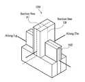
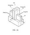
- FIG. 1Aillustrates a schematic of a FinFET showing different cross-section directions for FIG. 1B-FIG . 1 C.
- FIG. 1B-FIG . 1 Cillustrate cross sections of an accumulation type FinFET according to one aspect of the embodiment
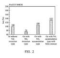
- FIG. 2illustrates a comparison of the turn-on current I on for embodiments of this embodiment and conventional devices
- FIG. 3illustrates a comparison of the bulk electron density for one embodiment of this embodiment and a conventional device
- FIG. 4illustrates a flow chart for a process to form an accumulation-type FinFET according to another aspect of this embodiment.
- FIG. 5illustrates cross sections of an integrated circuit including a dummy pattern and FinFET devices that have multiple accumulation type FinFET structures according to yet another aspect of the embodiment.
- Certain planar MOSFET using different material other than Sie.g. Ge planar MOS device has advantage over conventional Si planar MOS device, e.g. high carrier (electron/hole) mobility about 2.6/4 times higher than Si. It is found that Ge planar MOS device faces issues: 1) lower energy gap E g and high subthreshold leakage current I sub , 2) high dielectric constant ⁇ and short channel effect (SCE), and 3) high interface defects (Nit) causing poor carrier mobility ⁇ in Ge NMOS.
- Si planar MOS devicefaces issues: 1) lower energy gap E g and high subthreshold leakage current I sub , 2) high dielectric constant ⁇ and short channel effect (SCE), and 3) high interface defects (Nit) causing poor carrier mobility ⁇ in Ge NMOS.
- the planar MOSFETcan have the channel length that is in the same order of magnitude as the depletion-layer widths of the source and drain junction thereof.
- SCEdegrade the performance compared to other MOSFETs. As the channel length is reduced to increase both the operation speed and the number of components per chip, the SCE arise.
- the SECcan be attributed to two physical phenomena: 1) the limitation imposed on electron drift characteristics in the channel, and 2) the modification of the threshold voltage due to the shortening channel length.
- SCEincludes: 1) drain-induced barrier lowering (DIBL) and punch through, 2) surface scattering, 3) velocity saturation, 4) impact ionization, and 5) hot electrons.
- DIBLdrain-induced barrier lowering
- Ge planar-type MOSshows worse DIBL due to higher E.
- Ge NMOSIn the Ge NMOS, high Nit density is observed at the interface between the dielectric film layer and Ge near conduction band (Ec), which degrades electron mobility significantly.
- GeO (or other dielectric films) and Gedo not have desired interface compared to SiO 2 and Si system, where SiO 2 /Si has good interface that provides desired interface quality and low Nit for Si MOS.
- FIG. 1Aillustrates a schematic drawing of an exemplary FinFET.
- the FinFET 100can include a fin structure 102 .
- FIG. 1B-FIG . 1 Cillustrate cross sectional views of the accumulation-type FinFET 100 of FIG. 1A taken along section lines 1 B and 1 C, respectively.
- the accumulation-type FinFET 100shows a substrate 120 and a fin structure 102 on the substrate 120 .
- the fin structure 102includes a channel 108 between a source 106 and a drain 110 .
- the source 106 , the drain 110 , and the channel 108have the first type dopant.
- a well 112 under the source 106 , the drain 110 , and the channel 108has the second type dopant.
- the channel 108comprises Ge, SiGe, or III-V semiconductor.
- a gate dielectric layer 114is located over the channel 108 .
- a gate 116is located over the gate dielectric layer 114 .
- the source 106e.g., an n+ source region
- the source 106can be connected to a source voltage V S through a silicide 107 .
- the channel 108e.g., an n-channel region, can comprise, for example, a Ge fin region.
- the drain 110e.g., an n+ drain region, can be connected to a drain voltage V D through silicide 111 .
- a well 112e.g., p-type well, can provide electrical isolation from other devices.
- the gate dielectric layer 114can comprise oxide, nitride, oxynitride, high-k dielectric, or any combinations thereof.
- the gate 116e.g., a metal gate, is connected to a gate voltage V G .
- the oxide layer 115 and the nitride spacer 117are shown beside the gate 116 .
- the substrate 120can comprise Si, Ge, SiGe, III-V compound, and/or any combinations thereof.
- the high-k dielectric materialcan include hafnium silicate, zirconium silicate, hafnium dioxide, zirconium dioxide, other high-k dielectric material, or any combinations thereof.
- the channel 108can comprise SiGe or III-V semiconductor materials, e.g. AlGaAs, InGaAs, etc.
- the cross-sectional view of the accumulation-type FinFET 100shows the channel 108 , the gate dielectric layer 114 , and the gate 116 .
- the well 112 under the finprovides electrical isolation.
- the channel 108e.g. n ⁇ channel, comprises a Ge fin region.
- the well 112e.g. p-well, provides electrical isolation.
- the gate 116can be disposed over the gate dielectric layer 114 .
- Shallow trench isolation (STI) 118can be formed adjacent to the well 112 .
- the channel 108can comprise SiGe or III-V semiconductor materials, e.g. AlGaAs, InGaAs, etc.
- the channel 108 , the source 106 and the drain 110can have n-type dopants.
- the channel 108 , the source 106 , and the drain 110can have p-type dopants.
- the accumulation type FinFETcan change electron/hole profile and Fermi level (E F ) location that suppresses the effects of interface defects Nit.
- SiGe stressorscan be incorporated to the Ge FinFET NMOS to improve performance.
- the channel dopant concentration and/or the voltage VDD applied to the drain 110may affect electrical performances of the accumulation-type FinFET 100 .
- the counter doping density in channelis n-type/p-type 1e18 cm ⁇ 3 ⁇ 3e18 cm ⁇ 3 and the VDD is 0.5V.
- n-type channelcan decrease Fermi level (E F ), increase bulk electron density, thus reduces the effects of surface Nit.
- the electron densityis 7.1e12 cm ⁇ 2 , compared to an inversion type NMOS at 6.7e12 cm ⁇ 2 .
- low VDDshifts E F toward mid-bandgap, increases bulk electron/hole percentage, and reduces the effects of surface Nit in NMOS/PMOS.
- Ge and III-V semiconductor channel materialscan provide higher carrier mobility than Si. FinFET architecture provides better gate control, lower leakage currents and better scalability.
- the substrate 120can be Si or Ge substrate wafer. Above the substrate 120 , Ge epi can be performed to form Ge-fin for the channel 108 in one embodiment. In an NMOS embodiment, Ge can be also used for the source 106 or drain 110 . In some embodiments, a SiGe or Si source/drain is used since SiGe or Si source/drain would result in tensile stress in the channel 108 , e.g. Ge channel, to boost electron mobility. In PMOS source/drain region, Ge can be also used.
- GeSn, SiGeSn or III-V semiconductor source/drainis used, since GeSn, SiGeSn or III-V semiconductor source/drain would result in compressive stress in the channel 108 , e.g. Ge channel, to boost hole mobility.
- the FinFET structure with Ge fin channel region 108can help to reduce the SCE caused by high E. FinFET architecture can suppress leakage current in accumulation type device significantly. Compared to planar devices, FinFET structure can reduce the band-to-band tunneling (BTBT) leakage current significantly by lower channel doping (e.g. ⁇ 1e17 cm ⁇ 3 ) and reduced power supply voltage VDD.
- BTBTband-to-band tunneling
- FIG. 2illustrates a comparison of the turn-on current I on of an exemplary Ge accumulation FinFET and exemplary conventional devices. The results shown assume 80% electron mobility degradation in NMOS at the Fin surface region due to interface defects (traps) Nit in Ge devices.
- FIG. 2the turn-on current I on of a conventional inversion-type Si FinFET NMOS device without Nit is shown.
- the I on of Ge FinFETis normalized and compared to Si FinFET inversion-type.
- An inversion-type Ge FinFET NMOS device with Nitshows 74% I on , due to the electron mobility degradation at the fin surface from Nit in Ge.
- ⁇ 26% turn-on current I on degradation due to Nitis shown by TCAD simulation.
- the inversion-type Ge FinFET NMOS deviceis not accumulation-type and also has no stressors. However, with accumulation-type Ge FinFET NMOS device, the I on is increased to 108%, despite Nit in Ge.
- accumulation-type channel34% I on gain can be realized, which means that Ge with accumulation channel is 8% I on higher than Si FinFET. Further, with the addition of a SiGe stressor, the performance is further enhanced to 132% I on .
- desired surface passivation techniquescan further reduce the Nit of the Ge accumulation-type FinFET.
- narrower width of the fin regioncan suppress the turn-off leakage current I off and improve device performance affected by SCE/DIBL.
- less than 30 nm fin widthshows enhanced performance.
- high pocket dopingis required and accumulation-channel can be hard to be realized.
- accumulation-type devicesshow higher electron density in the bulk region, especially in low VDD and V G , e.g. 0.5V.
- FIG. 3illustrates a comparison of the bulk electron density for one embodiment and a conventional device.
- FIG. 4illustrates a flow chart for a process to form a FinFET according to another embodiment.
- a fin structureis formed on a substrate 120 , where the fin structure includes a channel 108 between a source 106 and a drain 110 (the source 106 , the drain 110 , and the channel 108 have the same type semiconductor and the channel 108 comprises Ge, SiGe, or III-V semiconductor).
- a gate dielectric layer 114e.g. oxide and/or a high-k dielectric
- a gate 116is formed over the gate dielectric layer 114 .
- the processcan further comprise depositing and etching shallow trench insulation (STI) 118 layer that provides isolation from adjacent devices.
- STIshallow trench insulation
- the processcan further comprise forming a well 112 below the source 106 , the drain 110 , and the channel 108 , wherein the well 112 has the second type dopant.
- the channel 108can have a dopant concentration between about 1e18 cm ⁇ 3 and about 3e18 cm ⁇ 3.
- the gate 116is capable of receiving a voltage, and the voltage is capable of shifting a Fermi-level of the channel toward a half of a bandgap of the channel.
- Forming the fin structurecan comprise defining a width of the channel 108 . In one embodiment, the width of channel 108 can be about 30 nm or less.
- At least one of the source 106 and the drain 110comprises Ge, SiGe, or Si for NMOS.
- At least one of the source 106 and the drain 110can comprise Ge, GeSn, SiGeSn or III-V semiconductor for PMOS.
- FIG. 5illustrates cross sections of an integrated circuit including a dummy pattern and FinFET devices that have multiple accumulation type FinFET structures according to yet another embodiment.
- the integrated circuitcomprises a substrate 120 , a dummy pattern 502 , and FinFET devices 504 and 506 .
- the dummy pattern 502includes at least one of a fin structure on the substrate.
- the fin structurecomprises a channel 508 between the first source and the first drain.
- the source, the drain, and the channel 508have the first type dopant.
- the well 112 providing electrical isolation from other devicescan have the second type dopant.
- FinFETs 504 and 506 on the substrate 120also includes fin structures on the substrate 120 .
- the fin structureincludes the channel 108 between a source and a drain.
- the source, the drain, and the second channel 108have the first type dopant.
- the channel 108comprises Ge, SiGe, or III-V semiconductor.
- a gate dielectric layer 114is located over the channel 108 .
- a gate 116is located over the gate dielectric layer 114 .
- multiple channels 108are used within one device.
- the devicehas an accumulation channel, thus FinFET devices 504 and 506 have the channel 108 , source, drain all the same type semiconductor, e.g. n-type/p-type for NMOS/PMOS respectively.
- the well 112is p-type for NMOS and n-type for PMOS, and shallow trench isolation (STI) 118 are used as device-to-device electrical and physical isolation, respectively.
- Dummy pattern 502 without gate 116can be also placed for better chemical mechanical planarization (CMP), etching, or fin-profile uniformity.
- the devicescan be formed on Si or Ge substrate 120 .
- the accumulation-type FinFETcan provide a desired electron or hole mobility that can increase device performance. Leakage current, interface defects (traps), and SCE effects that previously degraded conventional Ge planar-type MOS device are free from affecting the present embodiments, by using accumulation-type FinFET architecture.
- the present embodimentsapply not only to Ge channel, but also to SiGe, and other III-V channel material.
- the multi-fin within one device structurecan provide a higher current per footprint.
- Ge and siliconhave lattice mismatch, it is easier to grow good quality Ge epi layer in narrower fin width compared to wider fin width.
- the lattice mismatch induced stresscan be relaxed in narrow fin and the Ge epi has less defects and dislocations.
- the fin width of 50 nmis used in prior Ge device, it can be divided into two fins with 25 nm.
- a fin field-effect-transistorincluding a substrate and a fin structure on the substrate.
- the fin structureincludes a channel between a source and a drain, wherein the source, the drain, and the channel have a first type dopant, and the channel comprises at least one of a Ge, SiGe, or III-V semiconductor.
- the FinFETfurther includes a gate dielectric layer over the channel and a gate over the gate dielectric layer.
- the FinFETfurther includes a nitride spacer on the substrate adjacent the gate and an oxide layer between the nitride spacer and the gate and between the nitride spacer and the substrate.
- the methodincludes forming a fin structure on a substrate.
- the fin structureincluding a channel between a source and a drain, wherein the source, the drain, and the channel have a first type dopant, and the channel comprises at least one of a Ge, SiGe, or III-V semiconductor.
- the methodfurther includes forming a gate dielectric layer over the channel and forming a gate over the gate dielectric layer.
- the methodfurther includes forming a nitride spacer on the substrate adjacent the gate and forming an oxide layer between the nitride spacer and the gate and between the nitride spacer and the substrate.
- Still another aspect of this descriptionrelates to an integrated circuit including a substrate and a dummy pattern including at least one of a first fin structure on the substrate.
- the first fin structureincludes a first channel between a first source and a first drain, wherein the first source, the first drain, and the first channel have a first type dopant.
- the integrated circuitfurther includes a fin field-effect-transistor (FinFET) including a second fin structure on the substrate.
- the second fin structureincludes a channel between a source and a drain, wherein the source, the drain, and the channel have a first type dopant, and the channel comprises at least one of a Ge, SiGe, or III-V semiconductor.
- the FinFETfurther includes a gate dielectric layer over the channel and a gate over the gate dielectric layer.
- the FinFETfurther includes a nitride spacer on the substrate adjacent the gate and an oxide layer between the nitride spacer and the gate and between the nitride spacer and the substrate.
Landscapes
- Insulated Gate Type Field-Effect Transistor (AREA)
- Metal-Oxide And Bipolar Metal-Oxide Semiconductor Integrated Circuits (AREA)
- Thin Film Transistor (AREA)
Abstract
Description
- The present application is a continuation application of U.S. patent application Ser. No. 12/757,271, filed on Apr. 9, 2010, which claims priority of U.S. Provisional Patent Application Ser. No. 61/238,828, filed on Sep. 1, 2009, both of which are incorporated herein by reference in their entireties.
- The present application is related to U.S. patent application Ser. Nos. 12/707,788, filed on Feb. 18, 2010, (Docket Nos. TSMC2008-0432, T5057-R007U), titled MEMORY POWER GATING CIRCUIT AND METHODS; 12/758,426, filed on Apr. 12, 2010, (Docket Nos. TSMC2008-0582, T5057-Y048U), titled FINFETS AND METHODS FOR FORMING THE SAME; 12/731,325, filed on Mar. 25, 2010, (Docket Nos. TSMC2008-0597, T5057-B033U), titled ELECTRICAL FUSE AND RELATED APPLICATIONS; 12/724,556, filed on Mar. 16, 2010, (Docket Nos. TSMC2008-0598, T5057-K002U), titled ELECTRICAL ANTI-FUSE AND RELATED APPLICATIONS; 12/757,203, filed on Apr. 9, 2010, (Docket Nos. TSMC2009-0148, T5057-Y085U), titled STI STRUCTURE AND METHOD OF FORMING BOTTOM VOID IN SAME; 12/797,839, filed on Jun. 10, 2010, (Docket Nos. TSMC2009-0278, T5057-K099U), titled FIN STRUCTURE FOR HIGH MOBILITY MULTIPLE-GATE TRANSISTOR; 12/831,842, filed on Jul. 7, 2010, (Docket Nos. TSMC2009-0343, T5057-Y093U), titled METHOD FOR FORMING HIGH GERMANIUM CONCENTRATION SiGe STRESSOR; 12/761,686, filed on Apr. 16, 2010, (Docket Nos. TSMC2009-0442, T5057-Y125U), titled FINFETS AND METHODS FOR FORMING THE SAME; 12/766,233, filed on Apr. 23, 2010, (Docket Nos. TSMC2009-0444, T5057-K123U), titled FIN FIELD EFFECT TRANSISTOR; 12/757,271, filed on Apr. 9, 2010, (Docket Nos. TSMC2009-0445, T5057-Y113U), titled ACCUMULATION TYPE FINFET, CIRCUITS AND FABRICATION METHOD THEREOF; 12/694,846, filed on Jan. 27, 2010, (Docket Nos. TSMC2009-0646, T5057-Y165), titled INTEGRATED CIRCUITS AND METHODS FOR FORMING THE SAME; 12/638,958, filed on Dec. 14, 2009, (Docket Nos. TSMC2009-0738, T5057-B166), titled METHOD OF CONTROLLING GATE THICKNESS IN FORMING FINFET DEVICES; 12/768,884, filed on Apr. 28, 2010, (Docket Nos. TSMC2010-0028, T5057-Y228), titled METHODS FOR DOPING FIN FIELD-EFFECT TRANSISTORS; 12/731,411, filed on Mar. 25, 2010, (Docket Nos. TSMC2010-0057, T5057-B218), titled INTEGRATED CIRCUIT INCLUDING FINFETS AND METHODS FOR FORMING THE SAME; 12/775,006, filed on May 6, 2010, (Docket Nos. TSMC2010-0198, T5057-Y246), titled METHOD FOR FABRICATING A STRAINED STRUCTURE; 12/886,713, filed Sep. 21, 2010, (Docket Nos. TSMC2010-0646, T5057-B325), titled METHOD OF FORMING INTEGRATED CIRCUITS; 12/941,509, filed Nov. 8, 2010, (Docket Nos. TSMC2010-0561, T5057-B337), titled MECHANISMS FOR FORMING ULTRA SHALLOW JUNCTION; 12/900,626, filed Oct. 8, 2010, (Docket Nos. TSMC2010-0581, T5057-B330), titled TRANSISTOR HAVING NOTCHED FIN STRUCTURE AND METHOD OF MAKING THE SAME; 12/903,712, filed Oct. 13, 2010, (Docket Nos. TSMC2010-0731, T5057-R350), titled FINFET AND METHOD OF FABRICATING THE SAME; 61/412,846, filed Nov. 12, 2010, (Docket Nos. TSMC2010-0839, T5057-B388PRO), 61/394,418, filed Oct. 19, 2010, (Docket Nos. TSMC2010-0926, T5057-Y351PRO), titled METHODS OF FORMING GATE DIELECTRIC MATERIAL and 61/405,858, filed Oct. 22, 2010, (Docket Nos. TSMC2010-0928, T5057-R368PRO), titled METHODS OF FORMING SEMICONDUCTOR DEVICES.
- This disclosure relates generally to a semiconductor device, more particularly accumulation type FinFETs.
- As the integrated circuit size is reduced, there were efforts to overcome problems faced with such size reduction. For example, the performance of a MOSFET is degraded from reduced channel length, including leakage current. Therefore, new methods and structures to improve the MOSFET performance are desired.
- For a more complete understanding of the embodiment, and the advantages thereof, reference is now made to the following descriptions taken in conjunction with the accompanying drawings, in which:
FIG. 1A illustrates a schematic of a FinFET showing different cross-section directions forFIG. 1B-FIG .1C.FIG. 1B-FIG .1C illustrate cross sections of an accumulation type FinFET according to one aspect of the embodiment;FIG. 2 illustrates a comparison of the turn-on current Ionfor embodiments of this embodiment and conventional devices;FIG. 3 illustrates a comparison of the bulk electron density for one embodiment of this embodiment and a conventional device;FIG. 4 illustrates a flow chart for a process to form an accumulation-type FinFET according to another aspect of this embodiment; andFIG. 5 illustrates cross sections of an integrated circuit including a dummy pattern and FinFET devices that have multiple accumulation type FinFET structures according to yet another aspect of the embodiment.- The making and using of some embodiments are discussed in detail below. It should be appreciated, however, that the present embodiment provides many applicable novel concepts that can be embodied in a wide variety of specific contexts. The specific embodiments discussed are merely illustrative of specific ways to make and use the embodiment, and do not limit the scope of the invention.
- Certain planar MOSFET using different material other than Si, e.g. Ge planar MOS device has advantage over conventional Si planar MOS device, e.g. high carrier (electron/hole) mobility about 2.6/4 times higher than Si. It is found that Ge planar MOS device faces issues: 1) lower energy gap Egand high subthreshold leakage current Isub, 2) high dielectric constant ∈ and short channel effect (SCE), and 3) high interface defects (Nit) causing poor carrier mobility μ in Ge NMOS.
- When the channel length is shrinking down, the planar MOSFET can have the channel length that is in the same order of magnitude as the depletion-layer widths of the source and drain junction thereof. SCE degrade the performance compared to other MOSFETs. As the channel length is reduced to increase both the operation speed and the number of components per chip, the SCE arise. The SEC can be attributed to two physical phenomena: 1) the limitation imposed on electron drift characteristics in the channel, and 2) the modification of the threshold voltage due to the shortening channel length. SCE includes: 1) drain-induced barrier lowering (DIBL) and punch through, 2) surface scattering, 3) velocity saturation, 4) impact ionization, and 5) hot electrons. In particular, Ge planar-type MOS shows worse DIBL due to higher E.
- In the Ge NMOS, high Nit density is observed at the interface between the dielectric film layer and Ge near conduction band (Ec), which degrades electron mobility significantly. GeO (or other dielectric films) and Ge do not have desired interface compared to SiO2and Si system, where SiO2/Si has good interface that provides desired interface quality and low Nit for Si MOS.
- From the foregoing, MOSFET structures and methods for forming the MOSFET structures are desired. In exemplary embodiments, an accumulation type FinFET device is provided to improve MOSFET performances.
FIG. 1A illustrates a schematic drawing of an exemplary FinFET. InFIG. 1A , theFinFET 100 can include afin structure 102.FIG. 1B-FIG .1C illustrate cross sectional views of the accumulation-type FinFET 100 ofFIG. 1A taken alongsection lines FIG. 1A-FIG .1B, the accumulation-type FinFET 100 shows asubstrate 120 and afin structure 102 on thesubstrate 120. Thefin structure 102 includes achannel 108 between asource 106 and a drain110. Thesource 106, the drain110, and thechannel 108 have the first type dopant. A well112 under thesource 106, the drain110, and thechannel 108 has the second type dopant. Thechannel 108 comprises Ge, SiGe, or III-V semiconductor. Agate dielectric layer 114 is located over thechannel 108. Agate 116 is located over thegate dielectric layer 114. - In an embodiment forming an N-type accumulation Ge FinFET, the
source 106, e.g., an n+ source region, can be connected to a source voltage VSthrough asilicide 107. Thechannel 108, e.g., an n-channel region, can comprise, for example, a Ge fin region. The drain110, e.g., an n+ drain region, can be connected to a drain voltage VDthrough silicide111. A well112, e.g., p-type well, can provide electrical isolation from other devices. Thegate dielectric layer 114 can comprise oxide, nitride, oxynitride, high-k dielectric, or any combinations thereof. Thegate 116, e.g., a metal gate, is connected to a gate voltage VG. Theoxide layer 115 and the nitride spacer117 are shown beside thegate 116. Thesubstrate 120 can comprise Si, Ge, SiGe, III-V compound, and/or any combinations thereof. Examples of the high-k dielectric material can include hafnium silicate, zirconium silicate, hafnium dioxide, zirconium dioxide, other high-k dielectric material, or any combinations thereof. In other embodiments, thechannel 108 can comprise SiGe or III-V semiconductor materials, e.g. AlGaAs, InGaAs, etc. - In
FIG. 1C , the cross-sectional view of the accumulation-type FinFET 100 shows thechannel 108, thegate dielectric layer 114, and thegate 116. The well112 under the fin provides electrical isolation. In one embodiment, thechannel 108, e.g. n− channel, comprises a Ge fin region. The well112, e.g. p-well, provides electrical isolation. Thegate 116 can be disposed over thegate dielectric layer 114. Shallow trench isolation (STI)118 can be formed adjacent to thewell 112. In other embodiments, thechannel 108 can comprise SiGe or III-V semiconductor materials, e.g. AlGaAs, InGaAs, etc. - With an accumulation N-
type FinFET 102, thechannel 108, thesource 106 and the drain110 can have n-type dopants. In another embodiment for an accumulation P-type PMOS device, thechannel 108, thesource 106, and the drain110 can have p-type dopants. The accumulation type FinFET can change electron/hole profile and Fermi level (EF) location that suppresses the effects of interface defects Nit. Also, SiGe stressors can be incorporated to the Ge FinFET NMOS to improve performance. - For a conventional inversion type NMOS (with p-channel), electrons pile up at the interface and the device may suffer a mobility degradation due to Nit. Contrary to the conventional inversion-type NMOS, for an accumulation type NMOS, bulk inversion reduces the effect of Nit that can degrade sub-threshold current swing and electron mobility. Bulk inversion means that most inversion charges are located at bulk Fin region in the middle of the Fin in
FIG. 1C as bulk electrons while most electrons are plied up at gate-dielectric/Fin surface as surface electrons in the conventional surface inversion type device. Using VG=VDD, Fermi level of accumulation is nearer to the mid-bandgap (Eg), and the effects of Nit can be substantially reduced. - It is found that the channel dopant concentration and/or the voltage VDD applied to the drain110 may affect electrical performances of the accumulation-
type FinFET 100. For example, in one embodiment for NMOS/PMOS, the counter doping density in channel is n-type/p-type 1e18 cm−3˜3e18 cm−3and the VDD is 0.5V. In an NMOS accumulation-type device, n-type channel can decrease Fermi level (EF), increase bulk electron density, thus reduces the effects of surface Nit. For example, in one embodiment of an accumulation type NMOS, the electron density is 7.1e12 cm−2, compared to an inversion type NMOS at 6.7e12 cm−2. Also, low VDD shifts EFtoward mid-bandgap, increases bulk electron/hole percentage, and reduces the effects of surface Nit in NMOS/PMOS. - Ge and III-V semiconductor channel materials, e.g. AlGaAs, InGaAs, etc., can provide higher carrier mobility than Si. FinFET architecture provides better gate control, lower leakage currents and better scalability. The
substrate 120 can be Si or Ge substrate wafer. Above thesubstrate 120, Ge epi can be performed to form Ge-fin for thechannel 108 in one embodiment. In an NMOS embodiment, Ge can be also used for thesource 106 or drain110. In some embodiments, a SiGe or Si source/drain is used since SiGe or Si source/drain would result in tensile stress in thechannel 108, e.g. Ge channel, to boost electron mobility. In PMOS source/drain region, Ge can be also used. In some embodiments, GeSn, SiGeSn or III-V semiconductor source/drain is used, since GeSn, SiGeSn or III-V semiconductor source/drain would result in compressive stress in thechannel 108, e.g. Ge channel, to boost hole mobility. - The FinFET structure with Ge
fin channel region 108 can help to reduce the SCE caused by high E. FinFET architecture can suppress leakage current in accumulation type device significantly. Compared to planar devices, FinFET structure can reduce the band-to-band tunneling (BTBT) leakage current significantly by lower channel doping (e.g. ˜1e17 cm−3) and reduced power supply voltage VDD. FIG. 2 illustrates a comparison of the turn-on current Ionof an exemplary Ge accumulation FinFET and exemplary conventional devices. The results shown assume 80% electron mobility degradation in NMOS at the Fin surface region due to interface defects (traps) Nit in Ge devices.- In
FIG. 2 the turn-on current Ionof a conventional inversion-type Si FinFET NMOS device without Nit is shown. The Ionof Ge FinFET is normalized and compared to Si FinFET inversion-type. An inversion-type Ge FinFET NMOS device with Nit shows 74% Ion, due to the electron mobility degradation at the fin surface from Nit in Ge. In other words, compared to Si FinFET (inversion mode), −26% turn-on current Iondegradation due to Nit is shown by TCAD simulation. The inversion-type Ge FinFET NMOS device is not accumulation-type and also has no stressors. However, with accumulation-type Ge FinFET NMOS device, the Ionis increased to 108%, despite Nit in Ge. Therefore, by using accumulation-type channel, 34% Iongain can be realized, which means that Ge with accumulation channel is 8% Ionhigher than Si FinFET. Further, with the addition of a SiGe stressor, the performance is further enhanced to 132% Ion. In embodiments, desired surface passivation techniques can further reduce the Nit of the Ge accumulation-type FinFET. - In an accumulation-type device, narrower width of the fin region (Wfin) can suppress the turn-off leakage current Ioffand improve device performance affected by SCE/DIBL. In one embodiment, less than 30 nm fin width shows enhanced performance. In wide Wfinand planar devices, high pocket doping is required and accumulation-channel can be hard to be realized.
- Also, accumulation-type devices show higher electron density in the bulk region, especially in low VDD and VG, e.g. 0.5V.
FIG. 3 illustrates a comparison of the bulk electron density for one embodiment and a conventional device. In one embodiment, the accumulation-type Ge FinFET showed about 70% bulk electron density compared to the inversion type device with about 40% bulk electron density at VG=0.5V, as shown inFIG. 3 . The accumulation-type Ge FinFET NMOS device had the channel doping concentration of about 1e18 cm−3(N-type) and DIBL=105 mV/V, while the inversion-type device had the channel doping concentration of 5e18 cm−3(P-type). FIG. 4 illustrates a flow chart for a process to form a FinFET according to another embodiment. Atstep 402, a fin structure is formed on asubstrate 120, where the fin structure includes achannel 108 between asource 106 and a drain110 (thesource 106, the drain110, and thechannel 108 have the same type semiconductor and thechannel 108 comprises Ge, SiGe, or III-V semiconductor). Atstep 404, a gate dielectric layer114 (e.g. oxide and/or a high-k dielectric) is formed over thechannel 108. Atstep 406, agate 116 is formed over thegate dielectric layer 114. The process can further comprise depositing and etching shallow trench insulation (STI)118 layer that provides isolation from adjacent devices.- The process can further comprise forming a well112 below the
source 106, the drain110, and thechannel 108, wherein the well112 has the second type dopant. Thechannel 108 can have a dopant concentration between about 1e18 cm−3 and about 3e18 cm−3. Thegate 116 is capable of receiving a voltage, and the voltage is capable of shifting a Fermi-level of the channel toward a half of a bandgap of the channel. Forming the fin structure can comprise defining a width of thechannel 108. In one embodiment, the width ofchannel 108 can be about 30 nm or less. At least one of thesource 106 and the drain110 comprises Ge, SiGe, or Si for NMOS. At least one of thesource 106 and the drain110 can comprise Ge, GeSn, SiGeSn or III-V semiconductor for PMOS. FIG. 5 illustrates cross sections of an integrated circuit including a dummy pattern and FinFET devices that have multiple accumulation type FinFET structures according to yet another embodiment. The integrated circuit comprises asubstrate 120, adummy pattern 502, andFinFET devices dummy pattern 502 includes at least one of a fin structure on the substrate. The fin structure comprises achannel 508 between the first source and the first drain. The source, the drain, and thechannel 508 have the first type dopant. The well112 providing electrical isolation from other devices can have the second type dopant.FinFETs substrate 120 also includes fin structures on thesubstrate 120. The fin structure includes thechannel 108 between a source and a drain. The source, the drain, and thesecond channel 108 have the first type dopant. Thechannel 108 comprises Ge, SiGe, or III-V semiconductor. Agate dielectric layer 114 is located over thechannel 108. And agate 116 is located over thegate dielectric layer 114. In this embodiment,multiple channels 108 are used within one device.- The device has an accumulation channel, thus
FinFET devices channel 108, source, drain all the same type semiconductor, e.g. n-type/p-type for NMOS/PMOS respectively. The well112 is p-type for NMOS and n-type for PMOS, and shallow trench isolation (STI)118 are used as device-to-device electrical and physical isolation, respectively.Dummy pattern 502 withoutgate 116 can be also placed for better chemical mechanical planarization (CMP), etching, or fin-profile uniformity. The devices can be formed on Si orGe substrate 120. - From the foregoing, the accumulation-type FinFET can provide a desired electron or hole mobility that can increase device performance. Leakage current, interface defects (traps), and SCE effects that previously degraded conventional Ge planar-type MOS device are free from affecting the present embodiments, by using accumulation-type FinFET architecture. The present embodiments apply not only to Ge channel, but also to SiGe, and other III-V channel material.
- Further, the multi-fin within one device structure can provide a higher current per footprint. For example, since Ge and silicon have lattice mismatch, it is easier to grow good quality Ge epi layer in narrower fin width compared to wider fin width. The lattice mismatch induced stress can be relaxed in narrow fin and the Ge epi has less defects and dislocations. For example, if the fin width of 50 nm is used in prior Ge device, it can be divided into two fins with 25 nm. A skilled person in the art will appreciate that there can be many embodiment variations.
- One aspect of this description relates to a fin field-effect-transistor (FinFET) including a substrate and a fin structure on the substrate. The fin structure includes a channel between a source and a drain, wherein the source, the drain, and the channel have a first type dopant, and the channel comprises at least one of a Ge, SiGe, or III-V semiconductor. The FinFET further includes a gate dielectric layer over the channel and a gate over the gate dielectric layer. The FinFET further includes a nitride spacer on the substrate adjacent the gate and an oxide layer between the nitride spacer and the gate and between the nitride spacer and the substrate.
- Another aspect of this description relates to a method for forming a FinFET. The method includes forming a fin structure on a substrate. The fin structure including a channel between a source and a drain, wherein the source, the drain, and the channel have a first type dopant, and the channel comprises at least one of a Ge, SiGe, or III-V semiconductor. The method further includes forming a gate dielectric layer over the channel and forming a gate over the gate dielectric layer. The method further includes forming a nitride spacer on the substrate adjacent the gate and forming an oxide layer between the nitride spacer and the gate and between the nitride spacer and the substrate.
- Still another aspect of this description relates to an integrated circuit including a substrate and a dummy pattern including at least one of a first fin structure on the substrate. The first fin structure includes a first channel between a first source and a first drain, wherein the first source, the first drain, and the first channel have a first type dopant. The integrated circuit further includes a fin field-effect-transistor (FinFET) including a second fin structure on the substrate. The second fin structure includes a channel between a source and a drain, wherein the source, the drain, and the channel have a first type dopant, and the channel comprises at least one of a Ge, SiGe, or III-V semiconductor. The FinFET further includes a gate dielectric layer over the channel and a gate over the gate dielectric layer. The FinFET further includes a nitride spacer on the substrate adjacent the gate and an oxide layer between the nitride spacer and the gate and between the nitride spacer and the substrate.
- Although the present disclosure and its advantages have been described in detail, it should be understood that various changes, substitutions and alterations can be made herein without departing from the spirit and scope of the invention. Moreover, the scope of the present application is not intended to be limited to the particular embodiments of the process, machine, manufacture, and composition of matter, means, methods and steps described in the specification. As one of ordinary skill in the art will readily appreciate from the disclosure, processes, machines, manufacture, compositions of matter, means, methods, or steps, presently existing or later to be developed, that perform substantially the same function or achieve substantially the same result as the corresponding embodiments described herein may be utilized according to the present disclosure.
Claims (20)
1. A fin field-effect-transistor (FinFET), comprising:
a substrate;
a fin structure on the substrate, the fin structure including a channel between a source and a drain, wherein the source, the drain, and the channel have a first type dopant, and the channel comprises at least one of a Ge, SiGe, or III-V semiconductor;
a gate dielectric layer over the channel;
a gate over the gate dielectric layer;
a nitride spacer on the substrate adjacent the gate; and
an oxide layer between the nitride spacer and the gate and between the nitride spacer and the substrate.
2. The FinFET ofclaim 1 , wherein a doping concentration of the channel is lower than a doping concentration of the source and the drain.
3. The FinFET ofclaim 1 , further comprising a first silicide layer over the source and a second silicide layer over the drain.
4. The FinFET ofclaim 3 , wherein the nitride spacer extends over a top surface of the first and second silicide layers.
5. The FinFET ofclaim 1 , further comprising a well region that has a second type dopant below the source, the drain, and the channel.
6. The FinFET ofclaim 5 , further comprising at least one isolation feature adjacent to the well region below the source, the drain and the channel.
7. The FinFET ofclaim 1 , wherein the source and the drain are configured to induce tensile stress in the channel.
8. A method for forming a FinFET, comprising:
forming a fin structure on a substrate, the fin structure including a channel between a source and a drain, wherein the source, the drain, and the channel have a first type dopant, and the channel comprises at least one of a Ge, SiGe, or III-V semiconductor;
forming a gate dielectric layer over the channel;
forming a gate over the gate dielectric layer
forming a nitride spacer on the substrate adjacent the gate; and
forming an oxide layer between the nitride spacer and the gate and between the nitride spacer and the substrate.
9. The method ofclaim 8 , wherein forming the fin structure comprises doping the source and the drain with a higher doping concentration than the channel.
10. The method ofclaim 8 , further comprising forming a first silicide layer over the source and forming a second silicide layer over the drain.
11. The method ofclaim 10 , wherein forming the nitride spacer comprises forming the nitride spacer over a top surface of the first and second silicide layers.
12. The method ofclaim 8 , further comprising forming a well region that has a second type dopant below the source, the drain, and the channel.
13. The method ofclaim 12 , further comprising forming at least one isolation feature adjacent to the well region below the source, the drain and the channel.
14. The method ofclaim 8 , wherein forming the fin structure comprises inducing a tensile stress in the channel.
15. An integrated circuit, comprising:
a substrate;
a dummy pattern including at least one of a first fin structure on the substrate, the first fin structure comprising a first channel between a first source and a first drain, wherein the first source, the first drain, and the first channel have a first type dopant; and
a FinFET over the substrate, the FinFET including:
a second fin structure on the substrate, the second fin structure including a channel between a source and a drain, wherein the source, the drain, and the channel have a first type dopant, and the channel comprises at least one of a Ge, SiGe, or III-V semiconductor;
a gate dielectric layer over the channel;
a gate over the gate dielectric layer;
a nitride spacer on the substrate adjacent the gate; and
an oxide layer between the nitride spacer and the gate and between the nitride spacer and the substrate.
16. The integrated circuit ofclaim 15 , wherein a doping concentration of the channel is lower than a doping concentration of the source and the drain.
17. The integrated circuit ofclaim 15 , further comprising a first silicide layer over the source and a second silicide layer over the drain.
18. The integrated circuit ofclaim 17 , wherein the nitride spacer extends over a top surface of the first and second silicide layers.
19. The integrated circuit ofclaim 15 , further comprising:
a well region that has a second type dopant below the source, the drain, and the channel; and
at least one isolation feature adjacent to the well region below the source, the drain and the channel.
20. The integrated circuit ofclaim 15 , wherein the source and the drain are configured to induce tensile stress in the channel.
Priority Applications (1)
| Application Number | Priority Date | Filing Date | Title |
|---|---|---|---|
| US13/585,436US8896055B2 (en) | 2009-09-01 | 2012-08-14 | Accumulation type FinFET, circuits and fabrication method thereof |
Applications Claiming Priority (3)
| Application Number | Priority Date | Filing Date | Title |
|---|---|---|---|
| US23882809P | 2009-09-01 | 2009-09-01 | |
| US12/757,271US8264032B2 (en) | 2009-09-01 | 2010-04-09 | Accumulation type FinFET, circuits and fabrication method thereof |
| US13/585,436US8896055B2 (en) | 2009-09-01 | 2012-08-14 | Accumulation type FinFET, circuits and fabrication method thereof |
Related Parent Applications (1)
| Application Number | Title | Priority Date | Filing Date |
|---|---|---|---|
| US12/757,271ContinuationUS8264032B2 (en) | 2009-07-28 | 2010-04-09 | Accumulation type FinFET, circuits and fabrication method thereof |
Publications (2)
| Publication Number | Publication Date |
|---|---|
| US20120306002A1true US20120306002A1 (en) | 2012-12-06 |
| US8896055B2 US8896055B2 (en) | 2014-11-25 |
Family
ID=43623559
Family Applications (2)
| Application Number | Title | Priority Date | Filing Date |
|---|---|---|---|
| US12/757,271Active2030-09-22US8264032B2 (en) | 2009-07-28 | 2010-04-09 | Accumulation type FinFET, circuits and fabrication method thereof |
| US13/585,436Active2030-07-22US8896055B2 (en) | 2009-09-01 | 2012-08-14 | Accumulation type FinFET, circuits and fabrication method thereof |
Family Applications Before (1)
| Application Number | Title | Priority Date | Filing Date |
|---|---|---|---|
| US12/757,271Active2030-09-22US8264032B2 (en) | 2009-07-28 | 2010-04-09 | Accumulation type FinFET, circuits and fabrication method thereof |
Country Status (5)
| Country | Link |
|---|---|
| US (2) | US8264032B2 (en) |
| JP (1) | JP5373722B2 (en) |
| KR (2) | KR20110025075A (en) |
| CN (1) | CN102005477B (en) |
| TW (1) | TWI426607B (en) |
Cited By (10)
| Publication number | Priority date | Publication date | Assignee | Title |
|---|---|---|---|---|
| US20130153960A1 (en)* | 2011-12-16 | 2013-06-20 | Taiwan Semiconductor Manufacturing Company, Ltd. | Anti-Fuses on Semiconductor Fins |
| WO2014092846A1 (en)* | 2012-12-13 | 2014-06-19 | International Business Machines | Finfet with merge-free fins |
| WO2014209509A1 (en)* | 2013-06-24 | 2014-12-31 | International Business Machines Corporation | Semiconductor device including source/drain formed on bulk and gate channel formed on oxide layer |
| US8933435B2 (en)* | 2012-12-26 | 2015-01-13 | Globalfoundries Singapore Pte. Ltd. | Tunneling transistor |
| US8975125B2 (en) | 2013-03-14 | 2015-03-10 | International Business Machines Corporation | Formation of bulk SiGe fin with dielectric isolation by anodization |
| US9054192B1 (en) | 2013-12-20 | 2015-06-09 | International Business Machines Corporation | Integration of Ge-containing fins and compound semiconductor fins |
| US9105663B1 (en) | 2014-01-30 | 2015-08-11 | International Business Machines Corporation | FinFET with silicon germanium stressor and method of forming |
| US9673198B2 (en) | 2014-10-10 | 2017-06-06 | Samsung Electronics Co., Ltd. | Semiconductor devices having active regions at different levels |
| US9773865B2 (en)* | 2014-09-22 | 2017-09-26 | International Business Machines Corporation | Self-forming spacers using oxidation |
| US20190081058A1 (en)* | 2017-09-11 | 2019-03-14 | Renesas Electronics Corporation | Semiconductor device and manufacturing method therefor |
Families Citing this family (118)
| Publication number | Priority date | Publication date | Assignee | Title |
|---|---|---|---|---|
| US8440517B2 (en)* | 2010-10-13 | 2013-05-14 | Taiwan Semiconductor Manufacturing Company, Ltd. | FinFET and method of fabricating the same |
| US8492235B2 (en)* | 2010-12-29 | 2013-07-23 | Globalfoundries Singapore Pte. Ltd. | FinFET with stressors |
| CN102956483B (en)* | 2011-08-22 | 2015-06-03 | 中国科学院微电子研究所 | Semiconductor device structure and manufacturing method thereof |
| US8492206B2 (en) | 2011-08-22 | 2013-07-23 | Institute of Microelectronics, Chinese Academy of Sciences | Semiconductor device structure and method for manufacturing the same |
| US8969999B2 (en) | 2011-10-27 | 2015-03-03 | Taiwan Semiconductor Manufacturing Company, Ltd. | Fin-like field effect transistor (FinFET) based, metal-semiconductor alloy fuse device and method of manufacturing same |
| CN103107139B (en)* | 2011-11-09 | 2017-06-06 | 联华电子股份有限公司 | Structure of field effect transistor with fin structure and method of manufacturing the same |
| US8987824B2 (en) | 2011-11-22 | 2015-03-24 | Taiwan Semiconductor Manufacturing Co., Ltd. | Multi-gate semiconductor devices |
| CN103137685B (en)* | 2011-11-24 | 2015-09-30 | 中芯国际集成电路制造(北京)有限公司 | Semiconductor device and manufacture method thereof |
| US9397166B2 (en) | 2011-12-20 | 2016-07-19 | Intel Corporation | Strained channel region transistors employing source and drain stressors and systems including the same |
| WO2013095377A1 (en)* | 2011-12-20 | 2013-06-27 | Intel Corporation | Self-aligned contact metallization for reduced contact resistance |
| WO2013101237A1 (en) | 2011-12-31 | 2013-07-04 | Intel Corporation | Hard mask etch stop for tall fins |
| CN103187296B (en)* | 2011-12-31 | 2015-07-08 | 中芯国际集成电路制造(上海)有限公司 | Formation method of fin type field effect transistor |
| US9171925B2 (en)* | 2012-01-24 | 2015-10-27 | Taiwan Semiconductor Manufacturing Company, Ltd. | Multi-gate devices with replaced-channels and methods for forming the same |
| US9281378B2 (en) | 2012-01-24 | 2016-03-08 | Taiwan Semiconductor Manufacturing Company, Ltd. | Fin recess last process for FinFET fabrication |
| US8809178B2 (en) | 2012-02-29 | 2014-08-19 | Globalfoundries Inc. | Methods of forming bulk FinFET devices with replacement gates so as to reduce punch through leakage currents |
| US8836016B2 (en) | 2012-03-08 | 2014-09-16 | Taiwan Semiconductor Manufacturing Company, Ltd. | Semiconductor structures and methods with high mobility and high energy bandgap materials |
| US9082684B2 (en)* | 2012-04-02 | 2015-07-14 | Applied Materials, Inc. | Method of epitaxial doped germanium tin alloy formation |
| US8866195B2 (en)* | 2012-07-06 | 2014-10-21 | Taiwan Semiconductor Manufacturing Co., Ltd. | III-V compound semiconductor device having metal contacts and method of making the same |
| CN103426926B (en)* | 2012-05-14 | 2016-05-25 | 中芯国际集成电路制造(上海)有限公司 | Semiconductor structure and forming method thereof, PMOS transistor and forming method thereof |
| US8901615B2 (en) | 2012-06-13 | 2014-12-02 | Synopsys, Inc. | N-channel and P-channel end-to-end finfet cell architecture |
| US9583398B2 (en)* | 2012-06-29 | 2017-02-28 | Taiwan Semiconductor Manufacturing Company, Ltd. | Integrated circuit having FinFETS with different fin profiles |
| US8629420B1 (en)* | 2012-07-03 | 2014-01-14 | Intel Mobile Communications GmbH | Drain extended MOS device for bulk FinFET technology |
| US9142400B1 (en) | 2012-07-17 | 2015-09-22 | Stc.Unm | Method of making a heteroepitaxial layer on a seed area |
| CN102810555B (en)* | 2012-08-14 | 2015-04-15 | 北京大学 | Germanium tin tunneling field effect transistor and preparation method thereof |
| CN103594495A (en)* | 2012-08-16 | 2014-02-19 | 中国科学院微电子研究所 | Semiconductor device and method for manufacturing the same |
| US8912070B2 (en)* | 2012-08-16 | 2014-12-16 | The Institute of Microelectronics Chinese Academy of Science | Method for manufacturing semiconductor device |
| CN102832135A (en)* | 2012-09-05 | 2012-12-19 | 北京大学 | Method for preparing FinFET on germanium and III-V semiconductor material substrate |
| US9564367B2 (en)* | 2012-09-13 | 2017-02-07 | Globalfoundries Inc. | Methods of forming different FinFET devices with different threshold voltages and integrated circuit products containing such devices |
| US8890264B2 (en) | 2012-09-26 | 2014-11-18 | Intel Corporation | Non-planar III-V field effect transistors with conformal metal gate electrode and nitrogen doping of gate dielectric interface |
| US9287138B2 (en) | 2012-09-27 | 2016-03-15 | Taiwan Semiconductor Manufacturing Company, Ltd. | FinFET low resistivity contact formation method |
| US8823065B2 (en)* | 2012-11-08 | 2014-09-02 | Taiwan Semiconductor Manufacturing Company, Ltd. | Contact structure of semiconductor device |
| US9105490B2 (en) | 2012-09-27 | 2015-08-11 | Taiwan Semiconductor Manufacturing Company, Ltd. | Contact structure of semiconductor device |
| US8765563B2 (en)* | 2012-09-28 | 2014-07-01 | Intel Corporation | Trench confined epitaxially grown device layer(s) |
| US8633516B1 (en)* | 2012-09-28 | 2014-01-21 | Taiwan Semiconductor Manufacturing Company, Ltd. | Source/drain stack stressor for semiconductor device |
| US9082853B2 (en)* | 2012-10-31 | 2015-07-14 | International Business Machines Corporation | Bulk finFET with punchthrough stopper region and method of fabrication |
| CN103811341B (en)* | 2012-11-09 | 2016-05-11 | 中国科学院微电子研究所 | Semiconductor device and method for manufacturing the same |
| US9443962B2 (en) | 2012-11-09 | 2016-09-13 | Taiwan Semiconductor Manufacturing Company, Ltd. | Recessing STI to increase fin height in fin-first process |
| US8836018B2 (en)* | 2012-11-16 | 2014-09-16 | Taiwan Semiconductor Manufacturing Company, Ltd. | Semiconductor integrated device with channel region |
| CN103824775B (en)* | 2012-11-16 | 2018-04-24 | 中国科学院微电子研究所 | FinFET and manufacturing method thereof |
| US9093492B2 (en)* | 2012-11-29 | 2015-07-28 | Taiwan Semiconductor Manufacturing Company, Ltd. | Diode structure compatible with FinFET process |
| US8748940B1 (en) | 2012-12-17 | 2014-06-10 | Intel Corporation | Semiconductor devices with germanium-rich active layers and doped transition layers |
| US8896101B2 (en) | 2012-12-21 | 2014-11-25 | Intel Corporation | Nonplanar III-N transistors with compositionally graded semiconductor channels |
| US9093530B2 (en)* | 2012-12-28 | 2015-07-28 | Taiwan Semiconductor Manufacturing Company, Ltd. | Fin structure of FinFET |
| US20140264607A1 (en) | 2013-03-13 | 2014-09-18 | International Business Machines Corporation | Iii-v finfets on silicon substrate |
| US20140264488A1 (en)* | 2013-03-15 | 2014-09-18 | Globalfoundries Inc. | Methods of forming low defect replacement fins for a finfet semiconductor device and the resulting devices |
| US8940602B2 (en)* | 2013-04-11 | 2015-01-27 | International Business Machines Corporation | Self-aligned structure for bulk FinFET |
| US9412664B2 (en) | 2013-05-06 | 2016-08-09 | International Business Machines Corporation | Dual material finFET on single substrate |
| US8859355B1 (en)* | 2013-05-06 | 2014-10-14 | International Business Machines Corporation | Method to make dual material finFET on same substrate |
| US9293534B2 (en) | 2014-03-21 | 2016-03-22 | Taiwan Semiconductor Manufacturing Company, Ltd. | Formation of dislocations in source and drain regions of FinFET devices |
| CN104282561B (en)* | 2013-07-02 | 2018-11-06 | 中国科学院微电子研究所 | FinFET device and manufacturing method thereof |
| CN104282566B (en)* | 2013-07-03 | 2017-12-29 | 中芯国际集成电路制造(上海)有限公司 | Fin formula field effect transistor and forming method thereof |
| KR102176513B1 (en) | 2013-09-25 | 2020-11-09 | 인텔 코포레이션 | Isolation well doping with solid-state diffusion sources for finfet architectures |
| EP3050079A4 (en)* | 2013-09-26 | 2017-06-28 | Intel Corporation | Methods of forming low band gap source and drain structures in microelectronic devices |
| CN105493251A (en)* | 2013-09-27 | 2016-04-13 | 英特尔公司 | Non-planar semiconductor device with multi-layer flexible substrate |
| US9178045B2 (en)* | 2013-09-27 | 2015-11-03 | Samsung Electronics Co., Ltd. | Integrated circuit devices including FinFETS and methods of forming the same |
| US9583590B2 (en) | 2013-09-27 | 2017-02-28 | Samsung Electronics Co., Ltd. | Integrated circuit devices including FinFETs and methods of forming the same |
| US9184089B2 (en) | 2013-10-04 | 2015-11-10 | Taiwan Semiconductor Manufacturing Company, Ltd. | Mechanism of forming a trench structure |
| US9373720B2 (en)* | 2013-10-14 | 2016-06-21 | Globalfoundries Inc. | Three-dimensional transistor with improved channel mobility |
| US9312387B2 (en)* | 2013-11-01 | 2016-04-12 | Globalfoundries Inc. | Methods of forming FinFET devices with alternative channel materials |
| US9716176B2 (en) | 2013-11-26 | 2017-07-25 | Samsung Electronics Co., Ltd. | FinFET semiconductor devices including recessed source-drain regions on a bottom semiconductor layer and methods of fabricating the same |
| US10825738B2 (en)* | 2013-11-28 | 2020-11-03 | Institute of Microelectronics, Chinese Academy of Sciences | Semiconductor arrangements and methods of manufacturing the same |
| CN104671194B (en)* | 2013-12-03 | 2016-08-17 | 中芯国际集成电路制造(上海)有限公司 | Prevent MEMS that structure sheaf comes off and preparation method thereof |
| CN104733390B (en) | 2013-12-20 | 2018-06-26 | 台湾积体电路制造股份有限公司 | For the mechanism of FinFET traps doping |
| US9076869B1 (en) | 2014-01-08 | 2015-07-07 | Taiwan Semiconductor Manufacturing Company, Ltd. | FinFET device and method |
| US9048303B1 (en) | 2014-01-30 | 2015-06-02 | Infineon Technologies Austria Ag | Group III-nitride-based enhancement mode transistor |
| CN103839832A (en)* | 2014-02-25 | 2014-06-04 | 清华大学 | Fin type field effect transistor with GeSn source drain and forming method thereof |
| CN103840004A (en)* | 2014-02-25 | 2014-06-04 | 清华大学 | Fin type field effect transistor with SiGeSn source drain and forming method thereof |
| CN103855033A (en)* | 2014-02-25 | 2014-06-11 | 清华大学 | Finned field effect transistor with SiGeSn channels and forming method thereof |
| CN103840005A (en)* | 2014-02-25 | 2014-06-04 | 清华大学 | Fin type field effect transistor with SiGeSn source drain and forming method thereof |
| WO2015127701A1 (en)* | 2014-02-25 | 2015-09-03 | Tsinghua University | Method for forming fin field effect transistor |
| US9337279B2 (en) | 2014-03-03 | 2016-05-10 | Infineon Technologies Austria Ag | Group III-nitride-based enhancement mode transistor |
| US10468528B2 (en) | 2014-04-16 | 2019-11-05 | Taiwan Semiconductor Manufacturing Company, Ltd. | FinFET device with high-k metal gate stack |
| US9178067B1 (en) | 2014-04-25 | 2015-11-03 | Taiwan Semiconductor Manufacturing Company, Ltd. | Structure and method for FinFET device |
| US9721955B2 (en) | 2014-04-25 | 2017-08-01 | Taiwan Semiconductor Manufacturing Company, Ltd. | Structure and method for SRAM FinFET device having an oxide feature |
| JP6428789B2 (en) | 2014-06-24 | 2018-11-28 | インテル・コーポレーション | Integrated circuits, complementary metal oxide semiconductor (CMOS) devices, computing systems, and methods |
| US9224736B1 (en) | 2014-06-27 | 2015-12-29 | Taiwan Semicondcutor Manufacturing Company, Ltd. | Structure and method for SRAM FinFET device |
| US9842944B2 (en) | 2014-07-14 | 2017-12-12 | Intel Corporation | Solid-source diffused junction for fin-based electronics |
| US9735153B2 (en) | 2014-07-14 | 2017-08-15 | Samsung Electronics Co., Ltd. | Semiconductor device having fin-type field effect transistor and method of manufacturing the same |
| KR102263045B1 (en) | 2014-07-25 | 2021-06-10 | 삼성전자주식회사 | CMOS device with common strain-relaxed buffer and method for manufacturing thereof |
| US9276117B1 (en)* | 2014-08-19 | 2016-03-01 | Taiwan Semiconductor Manufacturing Company, Ltd. | Structure and method and FinFET device |
| US9293588B1 (en)* | 2014-08-28 | 2016-03-22 | International Business Machines Corporation | FinFET with a silicon germanium alloy channel and method of fabrication thereof |
| US10854735B2 (en) | 2014-09-03 | 2020-12-01 | Taiwan Semiconductor Manufacturing Company Limited | Method of forming transistor |
| US9847329B2 (en) | 2014-09-04 | 2017-12-19 | Taiwan Semiconductor Manufacturing Company, Ltd. | Structure of fin feature and method of making same |
| US9741811B2 (en) | 2014-12-15 | 2017-08-22 | Samsung Electronics Co., Ltd. | Integrated circuit devices including source/drain extension regions and methods of forming the same |
| EP3238262A4 (en)* | 2014-12-22 | 2018-12-19 | Intel Corporation | Prevention of subchannel leakage current |
| US9859423B2 (en)* | 2014-12-31 | 2018-01-02 | Stmicroelectronics, Inc. | Hetero-channel FinFET |
| US9601626B2 (en) | 2015-01-23 | 2017-03-21 | Taiwan Semiconductor Manufacturing Co., Ltd. | Semiconductor device including fin structure with two channel layers and manufacturing method thereof |
| US9537010B2 (en)* | 2015-02-04 | 2017-01-03 | Taiwan Semiconductor Manufacturing Co., Ltd. | Semiconductor device structure and method for forming the same |
| US9553172B2 (en) | 2015-02-11 | 2017-01-24 | Taiwan Semiconductor Manufacturing Company, Ltd. | Method and structure for FinFET devices |
| US9673112B2 (en)* | 2015-02-13 | 2017-06-06 | Taiwan Semiconductor Manufacturing Company, Ltd. | Method of semiconductor fabrication with height control through active region profile |
| KR102395071B1 (en) | 2015-05-14 | 2022-05-10 | 삼성전자주식회사 | Semiconductor devices including field effect transistors |
| US9761584B2 (en)* | 2015-06-05 | 2017-09-12 | Taiwan Semiconductor Manufacturing Co., Ltd. | Buried channel semiconductor device and method for manufacturing the same |
| KR102427071B1 (en)* | 2015-06-24 | 2022-08-01 | 인텔 코포레이션 | Sub-Fin Sidewall Passivation in Alternate Channel FinFETs |
| CN107667430B (en) | 2015-06-26 | 2022-07-22 | 英特尔公司 | High mobility semiconductor source/drain spacers |
| KR102352659B1 (en)* | 2015-06-27 | 2022-01-18 | 인텔 코포레이션 | Low Damage Self-Aligned Amphoteric FINFET Tip Doping |
| US9660025B2 (en)* | 2015-08-31 | 2017-05-23 | Taiwan Semiconductor Manufacturing Co., Ltd. | Structure and formation method of semiconductor device structure |
| US10446685B2 (en) | 2015-09-25 | 2019-10-15 | Intel Corporation | High-electron-mobility transistors with heterojunction dopant diffusion barrier |
| WO2017052608A1 (en) | 2015-09-25 | 2017-03-30 | Intel Corporation | High-electron-mobility transistors with counter-doped dopant diffusion barrier |
| WO2017052619A1 (en) | 2015-09-25 | 2017-03-30 | Intel Corporation | High mobility field effect transistors with a retrograded semiconductor source/drain |
| DE112015006974T5 (en) | 2015-09-25 | 2019-01-24 | Intel Corporation | A method of doping fin structures of non-planar transistor devices |
| US10411007B2 (en) | 2015-09-25 | 2019-09-10 | Intel Corporation | High mobility field effect transistors with a band-offset semiconductor source/drain spacer |
| KR102323943B1 (en) | 2015-10-21 | 2021-11-08 | 삼성전자주식회사 | Method of manufacturing semiconductor device |
| KR102509925B1 (en)* | 2015-12-03 | 2023-03-15 | 삼성전자주식회사 | Method of fabricating the semiconductor device |
| WO2017111958A1 (en)* | 2015-12-22 | 2017-06-29 | Intel Corporation | Transistors having ultra thin fin profiles and their methods of fabrication |
| WO2017111806A1 (en)* | 2015-12-24 | 2017-06-29 | Intel Corporation | Methods of forming doped source/drain contacts and structures formed thereby |
| US10466731B2 (en) | 2016-01-27 | 2019-11-05 | Taiwan Semiconductor Manufacturing Co., Ltd. | Two-transistor bandgap reference circuit and FinFET device suited for same |
| US10008580B2 (en)* | 2016-03-21 | 2018-06-26 | Samsung Electronics Co., Ltd. | FET including an InGaAs channel and method of enhancing performance of the FET |
| US10340383B2 (en)* | 2016-03-25 | 2019-07-02 | Taiwan Semiconductor Manufacturing Co., Ltd. | Semiconductor device having stressor layer |
| US10957769B2 (en) | 2016-06-17 | 2021-03-23 | Intel Corporation | High-mobility field effect transistors with wide bandgap fin cladding |
| US10580901B2 (en)* | 2016-09-02 | 2020-03-03 | International Business Machines Corporation | Stacked series connected VFETs for high voltage applications |
| US20180076281A1 (en)* | 2016-09-12 | 2018-03-15 | Jeng-Jye Shau | Deep channel isolated drain metal-oxide-semiconductor transistors |
| US20180076280A1 (en)* | 2016-09-12 | 2018-03-15 | Jeng-Jye Shau | Shallow drain metal-oxide-semiconductor transistors |
| US9847392B1 (en)* | 2016-10-11 | 2017-12-19 | United Microelectronics Corp. | Semiconductor device and method for fabricating the same |
| US10553494B2 (en) | 2016-11-29 | 2020-02-04 | Taiwan Semiconductor Manufacturing Company, Ltd. | Breakdown resistant semiconductor apparatus and method of making same |
| DE102018126911A1 (en) | 2017-11-30 | 2019-06-06 | Intel Corporation | Gate cut and fin trim isolation for advanced integrated circuit structure fabrication |
| KR20230006054A (en)* | 2017-11-30 | 2023-01-10 | 인텔 코포레이션 | Fin patterning for advanced integrated circuit structure fabrication |
| JP2020096000A (en)* | 2018-12-10 | 2020-06-18 | ソニーセミコンダクタソリューションズ株式会社 | Semiconductor device and manufacturing method of semiconductor device |
| US20220190159A1 (en)* | 2020-12-15 | 2022-06-16 | Intel Corporation | Integrated circuit structures having gesnb source or drain structures |
Citations (9)
| Publication number | Priority date | Publication date | Assignee | Title |
|---|---|---|---|---|
| US20050054164A1 (en)* | 2003-09-09 | 2005-03-10 | Advanced Micro Devices, Inc. | Strained silicon MOSFETs having reduced diffusion of n-type dopants |
| US7112495B2 (en)* | 2003-08-15 | 2006-09-26 | Taiwan Semiconductor Manufacturing Company, Ltd. | Structure and method of a strained channel transistor and a second semiconductor component in an integrated circuit |
| US20070048907A1 (en)* | 2005-08-24 | 2007-03-01 | Ho Lee | Methods of forming NMOS/PMOS transistors with source/drains including strained materials and devices so formed |
| US20070099370A1 (en)* | 2005-09-22 | 2007-05-03 | Kazuaki Nakajima | Method for manufacturing semiconductor device |
| US20080050865A1 (en)* | 2003-11-24 | 2008-02-28 | Samsung Electronics Co., Ltd. | Non-planar transistor having germanium channel region and method of manufacturing the same |
| US20090026553A1 (en)* | 2007-07-25 | 2009-01-29 | Krishna Kumar Bhuwalka | Tunnel Field-Effect Transistor with Narrow Band-Gap Channel and Strong Gate Coupling |
| US7989855B2 (en)* | 2004-06-10 | 2011-08-02 | Nec Corporation | Semiconductor device including a deflected part |
| US20120068273A1 (en)* | 2006-12-29 | 2012-03-22 | Fischer Kevin J | Stressed barrier plug slot contact structure for transistor performance enhancement |
| US20130005106A1 (en)* | 2006-06-30 | 2013-01-03 | Kabushiki Kaisha Toshiba | Field effect transistor, integrated circuit element, and method for manufacturing the same |
Family Cites Families (166)
| Publication number | Priority date | Publication date | Assignee | Title |
|---|---|---|---|---|
| JPH0590573A (en)* | 1991-09-30 | 1993-04-09 | Sharp Corp | Semiconductor device |
| JP2833946B2 (en) | 1992-12-08 | 1998-12-09 | 日本電気株式会社 | Etching method and apparatus |
| JP3144967B2 (en) | 1993-11-08 | 2001-03-12 | 株式会社日立製作所 | Semiconductor integrated circuit and method of manufacturing the same |
| KR0146203B1 (en) | 1995-06-26 | 1998-12-01 | 김광호 | Circuit element value adjusting circuit of semiconductor integrated circuit |
| US5963789A (en) | 1996-07-08 | 1999-10-05 | Kabushiki Kaisha Toshiba | Method for silicon island formation |
| JPH10223901A (en)* | 1996-12-04 | 1998-08-21 | Sony Corp | Field effect transistor and method of manufacturing the same |
| US6065481A (en) | 1997-03-26 | 2000-05-23 | Fsi International, Inc. | Direct vapor delivery of enabling chemical for enhanced HF etch process performance |
| TW468273B (en) | 1997-04-10 | 2001-12-11 | Hitachi Ltd | Semiconductor integrated circuit device and method for manufacturing the same |
| JP3660783B2 (en) | 1997-06-30 | 2005-06-15 | 松下電器産業株式会社 | Semiconductor integrated circuit |
| JP3586072B2 (en) | 1997-07-10 | 2004-11-10 | 株式会社東芝 | Nonvolatile semiconductor memory device |
| US6740247B1 (en) | 1999-02-05 | 2004-05-25 | Massachusetts Institute Of Technology | HF vapor phase wafer cleaning and oxide etching |
| JP4037029B2 (en)* | 2000-02-21 | 2008-01-23 | 株式会社ルネサステクノロジ | Semiconductor integrated circuit device |
| EP1292989A1 (en)* | 2000-05-10 | 2003-03-19 | Koninklijke Philips Electronics N.V. | A semiconductor device |
| JP4044721B2 (en) | 2000-08-15 | 2008-02-06 | 株式会社ルネサステクノロジ | Manufacturing method of semiconductor integrated circuit device |
| US6558477B1 (en) | 2000-10-16 | 2003-05-06 | Micron Technology, Inc. | Removal of photoresist through the use of hot deionized water bath, water vapor and ozone gas |
| US6830994B2 (en) | 2001-03-09 | 2004-12-14 | Semiconductor Energy Laboratory Co., Ltd. | Method of manufacturing a semiconductor device having a crystallized semiconductor film |
| US6531412B2 (en) | 2001-08-10 | 2003-03-11 | International Business Machines Corporation | Method for low temperature chemical vapor deposition of low-k films using selected cyclosiloxane and ozone gases for semiconductor applications |
| FR2830984B1 (en) | 2001-10-17 | 2005-02-25 | St Microelectronics Sa | INSULATION TRENCH AND METHOD OF MAKING SAME |
| US6737302B2 (en) | 2001-10-31 | 2004-05-18 | Semiconductor Energy Laboratory Co., Ltd. | Manufacturing method for field-effect transistor |
| US6621131B2 (en) | 2001-11-01 | 2003-09-16 | Intel Corporation | Semiconductor transistor having a stressed channel |
| JP4118045B2 (en) | 2001-12-07 | 2008-07-16 | 富士通株式会社 | Semiconductor device |
| US6642090B1 (en) | 2002-06-03 | 2003-11-04 | International Business Machines Corporation | Fin FET devices from bulk semiconductor and method for forming |
| JP2004014737A (en) | 2002-06-06 | 2004-01-15 | Renesas Technology Corp | Semiconductor device and its manufacture |
| US6812103B2 (en) | 2002-06-20 | 2004-11-02 | Micron Technology, Inc. | Methods of fabricating a dielectric plug in MOSFETS to suppress short-channel effects |
| US6974729B2 (en)* | 2002-07-16 | 2005-12-13 | Interuniversitair Microelektronica Centrum (Imec) | Integrated semiconductor fin device and a method for manufacturing such device |
| US7358121B2 (en) | 2002-08-23 | 2008-04-15 | Intel Corporation | Tri-gate devices and methods of fabrication |
| US6713365B2 (en) | 2002-09-04 | 2004-03-30 | Macronix International Co., Ltd. | Methods for filling shallow trench isolations having high aspect ratios |
| JP4031329B2 (en) | 2002-09-19 | 2008-01-09 | 株式会社東芝 | Semiconductor device and manufacturing method thereof |
| US6791155B1 (en) | 2002-09-20 | 2004-09-14 | Integrated Device Technology, Inc. | Stress-relieved shallow trench isolation (STI) structure and method for forming the same |
| US6833588B2 (en) | 2002-10-22 | 2004-12-21 | Advanced Micro Devices, Inc. | Semiconductor device having a U-shaped gate structure |
| US6706571B1 (en) | 2002-10-22 | 2004-03-16 | Advanced Micro Devices, Inc. | Method for forming multiple structures in a semiconductor device |
| US6946373B2 (en) | 2002-11-20 | 2005-09-20 | International Business Machines Corporation | Relaxed, low-defect SGOI for strained Si CMOS applications |
| US7087499B2 (en) | 2002-12-20 | 2006-08-08 | International Business Machines Corporation | Integrated antifuse structure for FINFET and CMOS devices |
| US20040192067A1 (en) | 2003-02-28 | 2004-09-30 | Bruno Ghyselen | Method for forming a relaxed or pseudo-relaxed useful layer on a substrate |
| DE10310740A1 (en) | 2003-03-10 | 2004-09-30 | Forschungszentrum Jülich GmbH | Method for producing a stress-relaxed layer structure on a non-lattice-matched substrate, and use of such a layer system in electronic and / or optoelectronic components |
| US6762448B1 (en) | 2003-04-03 | 2004-07-13 | Advanced Micro Devices, Inc. | FinFET device with multiple fin structures |
| US6838322B2 (en) | 2003-05-01 | 2005-01-04 | Freescale Semiconductor, Inc. | Method for forming a double-gated semiconductor device |
| US6872647B1 (en) | 2003-05-06 | 2005-03-29 | Advanced Micro Devices, Inc. | Method for forming multiple fins in a semiconductor device |
| US20060170053A1 (en)* | 2003-05-09 | 2006-08-03 | Yee-Chia Yeo | Accumulation mode multiple gate transistor |
| US7906441B2 (en) | 2003-05-13 | 2011-03-15 | Texas Instruments Incorporated | System and method for mitigating oxide growth in a gate dielectric |
| TWI242232B (en) | 2003-06-09 | 2005-10-21 | Canon Kk | Semiconductor substrate, semiconductor device, and method of manufacturing the same |
| US7456476B2 (en) | 2003-06-27 | 2008-11-25 | Intel Corporation | Nonplanar semiconductor device with partially or fully wrapped around gate electrode and methods of fabrication |
| KR100487567B1 (en)* | 2003-07-24 | 2005-05-03 | 삼성전자주식회사 | Method for fabricating a finfet in a semiconductor device |
| US7101742B2 (en) | 2003-08-12 | 2006-09-05 | Taiwan Semiconductor Manufacturing Company, Ltd. | Strained channel complementary field-effect transistors and methods of manufacture |
| US7172943B2 (en) | 2003-08-13 | 2007-02-06 | Taiwan Semiconductor Manufacturing Company, Ltd. | Multiple-gate transistors formed on bulk substrates |
| JP4212435B2 (en) | 2003-08-29 | 2009-01-21 | 株式会社東芝 | Semiconductor device and manufacturing method thereof |
| US7078312B1 (en) | 2003-09-02 | 2006-07-18 | Novellus Systems, Inc. | Method for controlling etch process repeatability |
| US6881668B2 (en) | 2003-09-05 | 2005-04-19 | Mosel Vitel, Inc. | Control of air gap position in a dielectric layer |
| JP2005116969A (en) | 2003-10-10 | 2005-04-28 | Toshiba Corp | Semiconductor device and manufacturing method thereof |
| US7303949B2 (en) | 2003-10-20 | 2007-12-04 | International Business Machines Corporation | High performance stress-enhanced MOSFETs using Si:C and SiGe epitaxial source/drain and method of manufacture |
| KR100513405B1 (en) | 2003-12-16 | 2005-09-09 | 삼성전자주식회사 | Method for forming fin field effect transistor |
| KR100702552B1 (en) | 2003-12-22 | 2007-04-04 | 인터내셔널 비지네스 머신즈 코포레이션 | Automated Layer Creation Method and Device for Double Gate FFT Design |
| KR100552058B1 (en)* | 2004-01-06 | 2006-02-20 | 삼성전자주식회사 | Semiconductor device having field effect transistor and manufacturing method thereof |
| KR100587672B1 (en) | 2004-02-02 | 2006-06-08 | 삼성전자주식회사 | Fin transistor formation method using damascene method |
| US6956277B1 (en) | 2004-03-23 | 2005-10-18 | Taiwan Semiconductor Manufacturing Company, Ltd. | Diode junction poly fuse |
| US7154118B2 (en) | 2004-03-31 | 2006-12-26 | Intel Corporation | Bulk non-planar transistor having strained enhanced mobility and methods of fabrication |
| US20050221591A1 (en) | 2004-04-06 | 2005-10-06 | International Business Machines Corporation | Method of forming high-quality relaxed SiGe alloy layers on bulk Si substrates |
| US7115920B2 (en) | 2004-04-12 | 2006-10-03 | International Business Machines Corporation | FinFET transistor and circuit |
| KR100568448B1 (en) | 2004-04-19 | 2006-04-07 | 삼성전자주식회사 | Manufacturing method of high dielectric film with reduced impurities |
| US7259050B2 (en) | 2004-04-29 | 2007-08-21 | Taiwan Semiconductor Manufacturing Company, Ltd. | Semiconductor device and method of making the same |
| US7300837B2 (en) | 2004-04-30 | 2007-11-27 | Taiwan Semiconductor Manufacturing Co., Ltd | FinFET transistor device on SOI and method of fabrication |
| KR100605104B1 (en) | 2004-05-04 | 2006-07-26 | 삼성전자주식회사 | Fin-Pet device and its manufacturing method |
| JP4493398B2 (en) | 2004-05-13 | 2010-06-30 | 富士通マイクロエレクトロニクス株式会社 | Semiconductor device |
| US7157351B2 (en) | 2004-05-20 | 2007-01-02 | Taiwan Semiconductor Manufacturing Co., Ltd. | Ozone vapor clean method |
| US20060153995A1 (en) | 2004-05-21 | 2006-07-13 | Applied Materials, Inc. | Method for fabricating a dielectric stack |
| JP4796329B2 (en)* | 2004-05-25 | 2011-10-19 | 三星電子株式会社 | Manufacturing method of multi-bridge channel type MOS transistor |
| US7015150B2 (en) | 2004-05-26 | 2006-03-21 | International Business Machines Corporation | Exposed pore sealing post patterning |
| KR100634372B1 (en) | 2004-06-04 | 2006-10-16 | 삼성전자주식회사 | Semiconductor Devices and Formation Methods |
| KR100604870B1 (en) | 2004-06-16 | 2006-07-31 | 삼성전자주식회사 | Field effect transistor and its manufacturing method which can improve the interruption of junction area |
| US7361563B2 (en) | 2004-06-17 | 2008-04-22 | Samsung Electronics Co., Ltd. | Methods of fabricating a semiconductor device using a selective epitaxial growth technique |
| JP5203558B2 (en) | 2004-08-20 | 2013-06-05 | 三星電子株式会社 | Transistor and manufacturing method thereof |
| TWI283066B (en) | 2004-09-07 | 2007-06-21 | Samsung Electronics Co Ltd | Field effect transistor (FET) having wire channels and method of fabricating the same |
| US7067400B2 (en) | 2004-09-17 | 2006-06-27 | International Business Machines Corporation | Method for preventing sidewall consumption during oxidation of SGOI islands |
| BRPI0515714A (en) | 2004-09-27 | 2008-07-29 | Dow Global Technologies Inc | A process for preparing a multilayer coating on the surface of an organic polymeric substrate by atmospheric pressure plasma deposition |
| US7018901B1 (en) | 2004-09-29 | 2006-03-28 | Freescale Semiconductor, Inc. | Method for forming a semiconductor device having a strained channel and a heterojunction source/drain |
| KR100652381B1 (en) | 2004-10-28 | 2006-12-01 | 삼성전자주식회사 | Multi-Bridge Channel Field Effect Transistor with Numerous Nanowire Channels and Manufacturing Method Thereof |
| KR100605499B1 (en) | 2004-11-02 | 2006-07-28 | 삼성전자주식회사 | Morse transistor having recessed gate electrode and manufacturing method thereof |
| KR100693783B1 (en) | 2004-11-04 | 2007-03-12 | 주식회사 하이닉스반도체 | Internal power generator |
| US7235472B2 (en) | 2004-11-12 | 2007-06-26 | Infineon Technologies Ag | Method of making fully silicided gate electrode |
| US7923339B2 (en) | 2004-12-06 | 2011-04-12 | Nxp B.V. | Method of producing an epitaxial layer on semiconductor substrate and device produced with such a method |
| KR100614800B1 (en)* | 2004-12-10 | 2006-08-22 | 삼성전자주식회사 | Method for manufacturing a transistor having a plurality of protruding channels |
| US7026232B1 (en) | 2004-12-23 | 2006-04-11 | Texas Instruments Incorporated | Systems and methods for low leakage strained-channel transistor |
| US20060151808A1 (en) | 2005-01-12 | 2006-07-13 | Chien-Hao Chen | MOSFET device with localized stressor |
| US7282766B2 (en) | 2005-01-17 | 2007-10-16 | Fujitsu Limited | Fin-type semiconductor device with low contact resistance |
| EP1851789B1 (en) | 2005-02-24 | 2013-05-01 | Soitec | Thermal oxidation of a sige layer and applications thereof |
| JP2006303451A (en) | 2005-03-23 | 2006-11-02 | Renesas Technology Corp | Semiconductor device and manufacturing method of semiconductor device |
| WO2006107942A1 (en) | 2005-04-05 | 2006-10-12 | Analog Devices, Inc. | Vapor hf etch process mask and method |
| JP2006324628A (en) | 2005-05-16 | 2006-11-30 | Interuniv Micro Electronica Centrum Vzw | Method for forming fully silicided gate and device obtained by the method |
| US7859065B2 (en)* | 2005-06-07 | 2010-12-28 | Nec Corporation | Fin-type field effect transistor and semiconductor device |
| JP4427489B2 (en) | 2005-06-13 | 2010-03-10 | 株式会社東芝 | Manufacturing method of semiconductor device |
| US7547637B2 (en) | 2005-06-21 | 2009-06-16 | Intel Corporation | Methods for patterning a semiconductor film |
| US7960791B2 (en) | 2005-06-24 | 2011-06-14 | International Business Machines Corporation | Dense pitch bulk FinFET process by selective EPI and etch |
| KR100655788B1 (en) | 2005-06-30 | 2006-12-08 | 삼성전자주식회사 | A method of cleaning a semiconductor device and a method of manufacturing a semiconductor device using the same. |
| US7279375B2 (en) | 2005-06-30 | 2007-10-09 | Intel Corporation | Block contact architectures for nanoscale channel transistors |
| US7247887B2 (en) | 2005-07-01 | 2007-07-24 | Synopsys, Inc. | Segmented channel MOS transistor |
| US7508031B2 (en) | 2005-07-01 | 2009-03-24 | Synopsys, Inc. | Enhanced segmented channel MOS transistor with narrowed base regions |
| US7190050B2 (en) | 2005-07-01 | 2007-03-13 | Synopsys, Inc. | Integrated circuit on corrugated substrate |
| US7807523B2 (en) | 2005-07-01 | 2010-10-05 | Synopsys, Inc. | Sequential selective epitaxial growth |
| US7265008B2 (en) | 2005-07-01 | 2007-09-04 | Synopsys, Inc. | Method of IC production using corrugated substrate |
| US8466490B2 (en) | 2005-07-01 | 2013-06-18 | Synopsys, Inc. | Enhanced segmented channel MOS transistor with multi layer regions |
| US7605449B2 (en) | 2005-07-01 | 2009-10-20 | Synopsys, Inc. | Enhanced segmented channel MOS transistor with high-permittivity dielectric isolation material |
| EP1744351A3 (en) | 2005-07-11 | 2008-11-26 | Interuniversitair Microelektronica Centrum ( Imec) | Method for forming a fully silicided gate MOSFET and devices obtained thereof |
| JP4774247B2 (en) | 2005-07-21 | 2011-09-14 | Okiセミコンダクタ株式会社 | Voltage regulator |
| KR101172853B1 (en) | 2005-07-22 | 2012-08-10 | 삼성전자주식회사 | Methods of forming semiconductor device |
| JP4749076B2 (en) | 2005-07-27 | 2011-08-17 | ルネサスエレクトロニクス株式会社 | Semiconductor device |
| US20070029576A1 (en) | 2005-08-03 | 2007-02-08 | International Business Machines Corporation | Programmable semiconductor device containing a vertically notched fusible link region and methods of making and using same |
| US7589387B2 (en) | 2005-10-05 | 2009-09-15 | Taiwan Semiconductor Manufacturing Company, Ltd. | SONOS type two-bit FinFET flash memory cell |
| US7425740B2 (en) | 2005-10-07 | 2008-09-16 | Taiwan Semiconductor Manufacturing Company, Ltd. | Method and structure for a 1T-RAM bit cell and macro |
| JP5167816B2 (en)* | 2005-10-21 | 2013-03-21 | 富士通株式会社 | Fin-type semiconductor device and manufacturing method thereof |
| US8513066B2 (en) | 2005-10-25 | 2013-08-20 | Freescale Semiconductor, Inc. | Method of making an inverted-T channel transistor |
| US7767541B2 (en) | 2005-10-26 | 2010-08-03 | International Business Machines Corporation | Methods for forming germanium-on-insulator semiconductor structures using a porous layer and semiconductor structures formed by these methods |
| DE102005052055B3 (en) | 2005-10-31 | 2007-04-26 | Advanced Micro Devices, Inc., Sunnyvale | Transistor and semiconductor components and production process for thin film silicon on insulator transistor has embedded deformed layer |
| US7718500B2 (en) | 2005-12-16 | 2010-05-18 | Chartered Semiconductor Manufacturing, Ltd | Formation of raised source/drain structures in NFET with embedded SiGe in PFET |
| US7525160B2 (en) | 2005-12-27 | 2009-04-28 | Intel Corporation | Multigate device with recessed strain regions |
| US20070152276A1 (en) | 2005-12-30 | 2007-07-05 | International Business Machines Corporation | High performance CMOS circuits, and methods for fabricating the same |
| US7410844B2 (en) | 2006-01-17 | 2008-08-12 | International Business Machines Corporation | Device fabrication by anisotropic wet etch |
| JP2007194336A (en) | 2006-01-18 | 2007-08-02 | Sumco Corp | Method for manufacturing semiconductor wafer |
| KR100827435B1 (en) | 2006-01-31 | 2008-05-06 | 삼성전자주식회사 | Gate Forming Method Using Oxygen-free Ashing Process in Semiconductor Devices |
| JP2007258485A (en)* | 2006-03-23 | 2007-10-04 | Toshiba Corp | Semiconductor device and manufacturing method thereof |
| US7407847B2 (en) | 2006-03-31 | 2008-08-05 | Intel Corporation | Stacked multi-gate transistor design and method of fabrication |
| KR100813527B1 (en) | 2006-04-06 | 2008-03-17 | 주식회사 하이닉스반도체 | Internal voltage generator of semiconductor memory |
| US8076189B2 (en) | 2006-04-11 | 2011-12-13 | Freescale Semiconductor, Inc. | Method of forming a semiconductor device and semiconductor device |
| US7663185B2 (en)* | 2006-05-27 | 2010-02-16 | Taiwan Semiconductor Manufacturing Co, Ltd | FIN-FET device structure formed employing bulk semiconductor substrate |
| DE602007000665D1 (en) | 2006-06-12 | 2009-04-23 | St Microelectronics Sa | Process for the preparation of Si1-yGey based zones with different Ge contents on one and the same substrate by means of condensation of germanium |
| US8211761B2 (en) | 2006-08-16 | 2012-07-03 | Globalfoundries Singapore Pte. Ltd. | Semiconductor system using germanium condensation |
| US7554110B2 (en) | 2006-09-15 | 2009-06-30 | Taiwan Semiconductor Manufacturing Company, Ltd. | MOS devices with partial stressor channel |
| US7494862B2 (en) | 2006-09-29 | 2009-02-24 | Intel Corporation | Methods for uniform doping of non-planar transistor structures |
| US7410854B2 (en) | 2006-10-05 | 2008-08-12 | Taiwan Semiconductor Manufacturing Company, Ltd. | Method of making FUSI gate and resulting structure |
| CN100527380C (en) | 2006-11-06 | 2009-08-12 | 北京北方微电子基地设备工艺研究中心有限责任公司 | Silicon chip shallow plow groove isolation etching method |
| US7534689B2 (en) | 2006-11-21 | 2009-05-19 | Advanced Micro Devices, Inc. | Stress enhanced MOS transistor and methods for its fabrication |
| US7943469B2 (en) | 2006-11-28 | 2011-05-17 | Intel Corporation | Multi-component strain-inducing semiconductor regions |
| US7538387B2 (en) | 2006-12-29 | 2009-05-26 | Taiwan Semiconductor Manufacturing Company, Ltd. | Stack SiGe for short channel improvement |
| US7456087B2 (en) | 2007-02-09 | 2008-11-25 | United Microelectronics Corp. | Semiconductor device and method of fabricating the same |
| JP2008227026A (en) | 2007-03-12 | 2008-09-25 | Toshiba Corp | Manufacturing method of semiconductor device |
| KR100844938B1 (en) | 2007-03-16 | 2008-07-09 | 주식회사 하이닉스반도체 | Semiconductor device and manufacturing method thereof |
| US8258029B2 (en) | 2007-04-10 | 2012-09-04 | Macronix International Co., Ltd. | Semiconductor structure and process for reducing the second bit effect of a memory device |
| US7727842B2 (en) | 2007-04-27 | 2010-06-01 | Texas Instruments Incorporated | Method of simultaneously siliciding a polysilicon gate and source/drain of a semiconductor device, and related device |
| US8174073B2 (en)* | 2007-05-30 | 2012-05-08 | Taiwan Semiconductor Manufacturing Co., Ltd. | Integrated circuit structures with multiple FinFETs |
| US7939862B2 (en) | 2007-05-30 | 2011-05-10 | Synopsys, Inc. | Stress-enhanced performance of a FinFet using surface/channel orientations and strained capping layers |
| TW200901368A (en) | 2007-06-23 | 2009-01-01 | Promos Technologies Inc | Shallow trench isolation structure and method for forming thereof |
| JP2009016418A (en) | 2007-07-02 | 2009-01-22 | Nec Electronics Corp | Semiconductor device |
| US7851865B2 (en) | 2007-10-17 | 2010-12-14 | International Business Machines Corporation | Fin-type field effect transistor structure with merged source/drain silicide and method of forming the structure |
| US8063437B2 (en) | 2007-07-27 | 2011-11-22 | Panasonic Corporation | Semiconductor device and method for producing the same |
| US8883597B2 (en)* | 2007-07-31 | 2014-11-11 | Taiwan Semiconductor Manufacturing Company, Ltd. | Method of fabrication of a FinFET element |
| US7692213B2 (en) | 2007-08-07 | 2010-04-06 | Chartered Semiconductor Manufacturing Ltd. | Integrated circuit system employing a condensation process |
| US20090053883A1 (en) | 2007-08-24 | 2009-02-26 | Texas Instruments Incorporated | Method of setting a work function of a fully silicided semiconductor device, and related device |
| JP4361102B2 (en) | 2007-09-12 | 2009-11-11 | 富士フイルム株式会社 | Method for manufacturing piezoelectric element |
| US7795097B2 (en) | 2007-11-20 | 2010-09-14 | Texas Instruments Incorporated | Semiconductor device manufactured by removing sidewalls during replacement gate integration scheme |
| US7767579B2 (en) | 2007-12-12 | 2010-08-03 | International Business Machines Corporation | Protection of SiGe during etch and clean operations |
| US20090166625A1 (en) | 2007-12-28 | 2009-07-02 | United Microelectronics Corp. | Mos device structure |
| US20110018065A1 (en) | 2008-02-26 | 2011-01-27 | Nxp B.V. | Method for manufacturing semiconductor device and semiconductor device |
| US8003466B2 (en) | 2008-04-08 | 2011-08-23 | Advanced Micro Devices, Inc. | Method of forming multiple fins for a semiconductor device |
| US8258585B2 (en) | 2008-05-29 | 2012-09-04 | Panasonic Corporation | Semiconductor device |
| DE102008030864B4 (en) | 2008-06-30 | 2010-06-17 | Advanced Micro Devices, Inc., Sunnyvale | Semiconductor device as a double-gate and tri-gate transistor, which are constructed on a solid substrate and method for producing the transistor |
| US7923321B2 (en) | 2008-11-03 | 2011-04-12 | Taiwan Semiconductor Manufacturing Company, Ltd. | Method for gap filling in a gate last process |
| US8247285B2 (en) | 2008-12-22 | 2012-08-21 | Taiwan Semiconductor Manufacturing Company, Ltd. | N-FET with a highly doped source/drain and strain booster |
| US8120063B2 (en) | 2008-12-29 | 2012-02-21 | Intel Corporation | Modulation-doped multi-gate devices |
| CA2659912C (en) | 2009-03-24 | 2012-04-24 | Sarah Mary Brunet | Nasal prong protector |
| US8236658B2 (en) | 2009-06-03 | 2012-08-07 | Taiwan Semiconductor Manufacturing Company, Ltd. | Methods for forming a transistor with a strained channel |
| US8759943B2 (en) | 2010-10-08 | 2014-06-24 | Taiwan Semiconductor Manufacturing Company, Ltd. | Transistor having notched fin structure and method of making the same |
| US8043920B2 (en) | 2009-09-17 | 2011-10-25 | International Business Machines Corporation | finFETS and methods of making same |
| US7993999B2 (en) | 2009-11-09 | 2011-08-09 | International Business Machines Corporation | High-K/metal gate CMOS finFET with improved pFET threshold voltage |
| US8114761B2 (en) | 2009-11-30 | 2012-02-14 | Applied Materials, Inc. | Method for doping non-planar transistors |
| US8088685B2 (en) | 2010-02-09 | 2012-01-03 | Taiwan Semiconductor Manufacturing Company, Ltd. | Integration of bottom-up metal film deposition |
| US8785286B2 (en) | 2010-02-09 | 2014-07-22 | Taiwan Semiconductor Manufacturing Company, Ltd. | Techniques for FinFET doping |
| US20110256682A1 (en) | 2010-04-15 | 2011-10-20 | Taiwan Semiconductor Manufacturing Company, Ltd. | Multiple Deposition, Multiple Treatment Dielectric Layer For A Semiconductor Device |
- 2010
- 2010-04-09USUS12/757,271patent/US8264032B2/enactiveActive
- 2010-08-11KRKR1020100077470Apatent/KR20110025075A/ennot_activeCeased
- 2010-08-25CNCN2010102638023Apatent/CN102005477B/enactiveActive
- 2010-08-27TWTW099128794Apatent/TWI426607B/enactive
- 2010-08-31JPJP2010194220Apatent/JP5373722B2/enactiveActive
- 2012
- 2012-08-14USUS13/585,436patent/US8896055B2/enactiveActive
- 2014
- 2014-06-19KRKR1020140074989Apatent/KR20140083964A/ennot_activeCeased
Patent Citations (9)
| Publication number | Priority date | Publication date | Assignee | Title |
|---|---|---|---|---|
| US7112495B2 (en)* | 2003-08-15 | 2006-09-26 | Taiwan Semiconductor Manufacturing Company, Ltd. | Structure and method of a strained channel transistor and a second semiconductor component in an integrated circuit |
| US20050054164A1 (en)* | 2003-09-09 | 2005-03-10 | Advanced Micro Devices, Inc. | Strained silicon MOSFETs having reduced diffusion of n-type dopants |
| US20080050865A1 (en)* | 2003-11-24 | 2008-02-28 | Samsung Electronics Co., Ltd. | Non-planar transistor having germanium channel region and method of manufacturing the same |
| US7989855B2 (en)* | 2004-06-10 | 2011-08-02 | Nec Corporation | Semiconductor device including a deflected part |
| US20070048907A1 (en)* | 2005-08-24 | 2007-03-01 | Ho Lee | Methods of forming NMOS/PMOS transistors with source/drains including strained materials and devices so formed |
| US20070099370A1 (en)* | 2005-09-22 | 2007-05-03 | Kazuaki Nakajima | Method for manufacturing semiconductor device |
| US20130005106A1 (en)* | 2006-06-30 | 2013-01-03 | Kabushiki Kaisha Toshiba | Field effect transistor, integrated circuit element, and method for manufacturing the same |
| US20120068273A1 (en)* | 2006-12-29 | 2012-03-22 | Fischer Kevin J | Stressed barrier plug slot contact structure for transistor performance enhancement |
| US20090026553A1 (en)* | 2007-07-25 | 2009-01-29 | Krishna Kumar Bhuwalka | Tunnel Field-Effect Transistor with Narrow Band-Gap Channel and Strong Gate Coupling |
Cited By (24)
| Publication number | Priority date | Publication date | Assignee | Title |
|---|---|---|---|---|
| US9412746B2 (en) | 2011-12-16 | 2016-08-09 | Taiwan Semiconductor Manufacturing Company, Ltd. | Anti-fuses on semiconductor fins |
| US8742457B2 (en)* | 2011-12-16 | 2014-06-03 | Taiwan Semiconductor Manufacturing Company, Ltd. | Anti-fuses on semiconductor fins |
| US20130153960A1 (en)* | 2011-12-16 | 2013-06-20 | Taiwan Semiconductor Manufacturing Company, Ltd. | Anti-Fuses on Semiconductor Fins |
| US9040370B2 (en) | 2011-12-16 | 2015-05-26 | Taiwan Semiconductor Manufacturing Company, Ltd. | Anti-fuses on semiconductor fins |
| WO2014092846A1 (en)* | 2012-12-13 | 2014-06-19 | International Business Machines | Finfet with merge-free fins |
| US10529858B2 (en) | 2012-12-13 | 2020-01-07 | Globalfoundries Inc. | FinFET with merge-free fins |
| US9947791B2 (en) | 2012-12-13 | 2018-04-17 | Globalfoundries Inc. | FinFET with merge-free fins |
| US8933435B2 (en)* | 2012-12-26 | 2015-01-13 | Globalfoundries Singapore Pte. Ltd. | Tunneling transistor |
| US9508851B2 (en)* | 2013-03-14 | 2016-11-29 | International Business Machines Corporation | Formation of bulk SiGe fin with dielectric isolation by anodization |
| US8975125B2 (en) | 2013-03-14 | 2015-03-10 | International Business Machines Corporation | Formation of bulk SiGe fin with dielectric isolation by anodization |
| US8957478B2 (en) | 2013-06-24 | 2015-02-17 | International Business Machines Corporation | Semiconductor device including source/drain formed on bulk and gate channel formed on oxide layer |
| US9059019B2 (en) | 2013-06-24 | 2015-06-16 | International Business Machines Corporation | Semiconductor device including source/drain formed on bulk and gate channel formed on oxide layer |
| WO2014209509A1 (en)* | 2013-06-24 | 2014-12-31 | International Business Machines Corporation | Semiconductor device including source/drain formed on bulk and gate channel formed on oxide layer |
| US9054192B1 (en) | 2013-12-20 | 2015-06-09 | International Business Machines Corporation | Integration of Ge-containing fins and compound semiconductor fins |
| US9105663B1 (en) | 2014-01-30 | 2015-08-11 | International Business Machines Corporation | FinFET with silicon germanium stressor and method of forming |
| US10566417B2 (en) | 2014-09-22 | 2020-02-18 | International Business Machines Corporation | Self-forming spacers using oxidation |
| US10068967B2 (en) | 2014-09-22 | 2018-09-04 | International Business Machines Corporation | Self-forming spacers using oxidation |
| US9773865B2 (en)* | 2014-09-22 | 2017-09-26 | International Business Machines Corporation | Self-forming spacers using oxidation |
| US10833156B2 (en) | 2014-09-22 | 2020-11-10 | Elpis Technologies Inc. | Self-forming spacers using oxidation |
| US9673198B2 (en) | 2014-10-10 | 2017-06-06 | Samsung Electronics Co., Ltd. | Semiconductor devices having active regions at different levels |
| US20190081058A1 (en)* | 2017-09-11 | 2019-03-14 | Renesas Electronics Corporation | Semiconductor device and manufacturing method therefor |
| CN109494225A (en)* | 2017-09-11 | 2019-03-19 | 瑞萨电子株式会社 | Semiconductor devices and its manufacturing method |
| US10622371B2 (en)* | 2017-09-11 | 2020-04-14 | Renesas Electronics Corporation | Semiconductor device and manufacturing method therefor |
| CN109494225B (en)* | 2017-09-11 | 2023-09-29 | 瑞萨电子株式会社 | Semiconductor device and method for manufacturing the same |
Also Published As
| Publication number | Publication date |
|---|---|
| JP2011061196A (en) | 2011-03-24 |
| US20110049613A1 (en) | 2011-03-03 |
| CN102005477B (en) | 2013-10-02 |
| US8264032B2 (en) | 2012-09-11 |
| KR20140083964A (en) | 2014-07-04 |
| TW201110352A (en) | 2011-03-16 |
| US8896055B2 (en) | 2014-11-25 |
| KR20110025075A (en) | 2011-03-09 |
| JP5373722B2 (en) | 2013-12-18 |
| CN102005477A (en) | 2011-04-06 |
| TWI426607B (en) | 2014-02-11 |
Similar Documents
| Publication | Publication Date | Title |
|---|---|---|
| US8896055B2 (en) | Accumulation type FinFET, circuits and fabrication method thereof | |
| US10109748B2 (en) | High-mobility multiple-gate transistor with improved on-to-off current ratio | |
| US10164099B2 (en) | Device with diffusion blocking layer in source/drain region | |
| US7834345B2 (en) | Tunnel field-effect transistors with superlattice channels | |
| US7824968B2 (en) | LDMOS using a combination of enhanced dielectric stress layer and dummy gates | |
| US8587075B2 (en) | Tunnel field-effect transistor with metal source | |
| US9698270B2 (en) | FinFET with dual workfunction gate structure | |
| US7612364B2 (en) | MOS devices with source/drain regions having stressed regions and non-stressed regions | |
| US11183591B2 (en) | Lateral double-diffused metal-oxide-semiconductor (LDMOS) fin field effect transistor with enhanced capabilities | |
| US20210327716A1 (en) | Semiconductor device and method for fabricating the same including re-growth process to form non-uniform gate dielectric layer | |
| US9478663B2 (en) | FinFET device including a uniform silicon alloy fin | |
| US9634002B1 (en) | Semiconductor device and method of manufacturing the same | |
| US9634123B2 (en) | FinFET device including a dielectrically isolated silicon alloy fin | |
| US9142674B2 (en) | FINFET devices having a body contact and methods of forming the same | |
| US20060172477A1 (en) | MOS field effect transistor and manufacture method therefor | |
| US9406803B2 (en) | FinFET device including a uniform silicon alloy fin | |
| KR20100073416A (en) | Semiconductor device and method for manufacturing the same |
Legal Events
| Date | Code | Title | Description |
|---|---|---|---|
| AS | Assignment | Owner name:TAIWAN SEMICONDUCTOR MANUFACTURING COMPANY, LTD., Free format text:ASSIGNMENT OF ASSIGNORS INTEREST;ASSIGNORS:YEH, CHIH CHIEH;CHANG, CHIH-SHENG;WANN, CLEMENT HSINGJEN;SIGNING DATES FROM 20100311 TO 20100323;REEL/FRAME:028784/0889 | |
| STCF | Information on status: patent grant | Free format text:PATENTED CASE | |
| MAFP | Maintenance fee payment | Free format text:PAYMENT OF MAINTENANCE FEE, 4TH YEAR, LARGE ENTITY (ORIGINAL EVENT CODE: M1551) Year of fee payment:4 | |
| MAFP | Maintenance fee payment | Free format text:PAYMENT OF MAINTENANCE FEE, 8TH YEAR, LARGE ENTITY (ORIGINAL EVENT CODE: M1552); ENTITY STATUS OF PATENT OWNER: LARGE ENTITY Year of fee payment:8 |