US20120301149A1 - Method And System For Hybrid Integration Of Optical Communication Systems - Google Patents
Method And System For Hybrid Integration Of Optical Communication SystemsDownload PDFInfo
- Publication number
- US20120301149A1 US20120301149A1US13/568,406US201213568406AUS2012301149A1US 20120301149 A1US20120301149 A1US 20120301149A1US 201213568406 AUS201213568406 AUS 201213568406AUS 2012301149 A1US2012301149 A1US 2012301149A1
- Authority
- US
- United States
- Prior art keywords
- optical
- die
- silicon photonics
- photonics die
- signals
- Prior art date
- Legal status (The legal status is an assumption and is not a legal conclusion. Google has not performed a legal analysis and makes no representation as to the accuracy of the status listed.)
- Granted
Links
Images


Classifications
- G—PHYSICS
- G02—OPTICS
- G02B—OPTICAL ELEMENTS, SYSTEMS OR APPARATUS
- G02B6/00—Light guides; Structural details of arrangements comprising light guides and other optical elements, e.g. couplings
- G02B6/24—Coupling light guides
- G02B6/42—Coupling light guides with opto-electronic elements
- G02B6/4201—Packages, e.g. shape, construction, internal or external details
- G02B6/4274—Electrical aspects
- G02B6/428—Electrical aspects containing printed circuit boards [PCB]
- G—PHYSICS
- G02—OPTICS
- G02B—OPTICAL ELEMENTS, SYSTEMS OR APPARATUS
- G02B6/00—Light guides; Structural details of arrangements comprising light guides and other optical elements, e.g. couplings
- G02B6/10—Light guides; Structural details of arrangements comprising light guides and other optical elements, e.g. couplings of the optical waveguide type
- G02B6/12—Light guides; Structural details of arrangements comprising light guides and other optical elements, e.g. couplings of the optical waveguide type of the integrated circuit kind
- G02B6/12004—Combinations of two or more optical elements
- G—PHYSICS
- G02—OPTICS
- G02B—OPTICAL ELEMENTS, SYSTEMS OR APPARATUS
- G02B6/00—Light guides; Structural details of arrangements comprising light guides and other optical elements, e.g. couplings
- G02B6/24—Coupling light guides
- G02B6/26—Optical coupling means
- G02B6/34—Optical coupling means utilising prism or grating
- G—PHYSICS
- G02—OPTICS
- G02B—OPTICAL ELEMENTS, SYSTEMS OR APPARATUS
- G02B6/00—Light guides; Structural details of arrangements comprising light guides and other optical elements, e.g. couplings
- G02B6/24—Coupling light guides
- G02B6/42—Coupling light guides with opto-electronic elements
- G02B6/4295—Coupling light guides with opto-electronic elements coupling with semiconductor devices activated by light through the light guide, e.g. thyristors, phototransistors
- G—PHYSICS
- G02—OPTICS
- G02F—OPTICAL DEVICES OR ARRANGEMENTS FOR THE CONTROL OF LIGHT BY MODIFICATION OF THE OPTICAL PROPERTIES OF THE MEDIA OF THE ELEMENTS INVOLVED THEREIN; NON-LINEAR OPTICS; FREQUENCY-CHANGING OF LIGHT; OPTICAL LOGIC ELEMENTS; OPTICAL ANALOGUE/DIGITAL CONVERTERS
- G02F1/00—Devices or arrangements for the control of the intensity, colour, phase, polarisation or direction of light arriving from an independent light source, e.g. switching, gating or modulating; Non-linear optics
- G02F1/01—Devices or arrangements for the control of the intensity, colour, phase, polarisation or direction of light arriving from an independent light source, e.g. switching, gating or modulating; Non-linear optics for the control of the intensity, phase, polarisation or colour
- G02F1/21—Devices or arrangements for the control of the intensity, colour, phase, polarisation or direction of light arriving from an independent light source, e.g. switching, gating or modulating; Non-linear optics for the control of the intensity, phase, polarisation or colour by interference
- G02F1/225—Devices or arrangements for the control of the intensity, colour, phase, polarisation or direction of light arriving from an independent light source, e.g. switching, gating or modulating; Non-linear optics for the control of the intensity, phase, polarisation or colour by interference in an optical waveguide structure
- G02F1/2255—Devices or arrangements for the control of the intensity, colour, phase, polarisation or direction of light arriving from an independent light source, e.g. switching, gating or modulating; Non-linear optics for the control of the intensity, phase, polarisation or colour by interference in an optical waveguide structure controlled by a high-frequency electromagnetic component in an electric waveguide structure
- G—PHYSICS
- G02—OPTICS
- G02F—OPTICAL DEVICES OR ARRANGEMENTS FOR THE CONTROL OF LIGHT BY MODIFICATION OF THE OPTICAL PROPERTIES OF THE MEDIA OF THE ELEMENTS INVOLVED THEREIN; NON-LINEAR OPTICS; FREQUENCY-CHANGING OF LIGHT; OPTICAL LOGIC ELEMENTS; OPTICAL ANALOGUE/DIGITAL CONVERTERS
- G02F1/00—Devices or arrangements for the control of the intensity, colour, phase, polarisation or direction of light arriving from an independent light source, e.g. switching, gating or modulating; Non-linear optics
- G02F1/01—Devices or arrangements for the control of the intensity, colour, phase, polarisation or direction of light arriving from an independent light source, e.g. switching, gating or modulating; Non-linear optics for the control of the intensity, phase, polarisation or colour
- G02F1/21—Devices or arrangements for the control of the intensity, colour, phase, polarisation or direction of light arriving from an independent light source, e.g. switching, gating or modulating; Non-linear optics for the control of the intensity, phase, polarisation or colour by interference
- G02F1/225—Devices or arrangements for the control of the intensity, colour, phase, polarisation or direction of light arriving from an independent light source, e.g. switching, gating or modulating; Non-linear optics for the control of the intensity, phase, polarisation or colour by interference in an optical waveguide structure
- G02F1/2257—Devices or arrangements for the control of the intensity, colour, phase, polarisation or direction of light arriving from an independent light source, e.g. switching, gating or modulating; Non-linear optics for the control of the intensity, phase, polarisation or colour by interference in an optical waveguide structure the optical waveguides being made of semiconducting material
- H—ELECTRICITY
- H01—ELECTRIC ELEMENTS
- H01L—SEMICONDUCTOR DEVICES NOT COVERED BY CLASS H10
- H01L25/00—Assemblies consisting of a plurality of semiconductor or other solid state devices
- H01L25/03—Assemblies consisting of a plurality of semiconductor or other solid state devices all the devices being of a type provided for in a single subclass of subclasses H10B, H10D, H10F, H10H, H10K or H10N, e.g. assemblies of rectifier diodes
- H01L25/04—Assemblies consisting of a plurality of semiconductor or other solid state devices all the devices being of a type provided for in a single subclass of subclasses H10B, H10D, H10F, H10H, H10K or H10N, e.g. assemblies of rectifier diodes the devices not having separate containers
- H01L25/065—Assemblies consisting of a plurality of semiconductor or other solid state devices all the devices being of a type provided for in a single subclass of subclasses H10B, H10D, H10F, H10H, H10K or H10N, e.g. assemblies of rectifier diodes the devices not having separate containers the devices being of a type provided for in group H10D89/00
- H01L25/0652—Assemblies consisting of a plurality of semiconductor or other solid state devices all the devices being of a type provided for in a single subclass of subclasses H10B, H10D, H10F, H10H, H10K or H10N, e.g. assemblies of rectifier diodes the devices not having separate containers the devices being of a type provided for in group H10D89/00 the devices being arranged next and on each other, i.e. mixed assemblies
- H—ELECTRICITY
- H04—ELECTRIC COMMUNICATION TECHNIQUE
- H04B—TRANSMISSION
- H04B10/00—Transmission systems employing electromagnetic waves other than radio-waves, e.g. infrared, visible or ultraviolet light, or employing corpuscular radiation, e.g. quantum communication
- H04B10/27—Arrangements for networking
- H—ELECTRICITY
- H10—SEMICONDUCTOR DEVICES; ELECTRIC SOLID-STATE DEVICES NOT OTHERWISE PROVIDED FOR
- H10D—INORGANIC ELECTRIC SEMICONDUCTOR DEVICES
- H10D86/00—Integrated devices formed in or on insulating or conducting substrates, e.g. formed in silicon-on-insulator [SOI] substrates or on stainless steel or glass substrates
- H10D86/01—Manufacture or treatment
- H—ELECTRICITY
- H10—SEMICONDUCTOR DEVICES; ELECTRIC SOLID-STATE DEVICES NOT OTHERWISE PROVIDED FOR
- H10D—INORGANIC ELECTRIC SEMICONDUCTOR DEVICES
- H10D86/00—Integrated devices formed in or on insulating or conducting substrates, e.g. formed in silicon-on-insulator [SOI] substrates or on stainless steel or glass substrates
- H10D86/201—Integrated devices formed in or on insulating or conducting substrates, e.g. formed in silicon-on-insulator [SOI] substrates or on stainless steel or glass substrates the substrates comprising an insulating layer on a semiconductor body, e.g. SOI
- H—ELECTRICITY
- H10—SEMICONDUCTOR DEVICES; ELECTRIC SOLID-STATE DEVICES NOT OTHERWISE PROVIDED FOR
- H10D—INORGANIC ELECTRIC SEMICONDUCTOR DEVICES
- H10D88/00—Three-dimensional [3D] integrated devices
- G—PHYSICS
- G02—OPTICS
- G02B—OPTICAL ELEMENTS, SYSTEMS OR APPARATUS
- G02B6/00—Light guides; Structural details of arrangements comprising light guides and other optical elements, e.g. couplings
- G02B6/10—Light guides; Structural details of arrangements comprising light guides and other optical elements, e.g. couplings of the optical waveguide type
- G02B6/12—Light guides; Structural details of arrangements comprising light guides and other optical elements, e.g. couplings of the optical waveguide type of the integrated circuit kind
- G02B2006/12083—Constructional arrangements
- G02B2006/12107—Grating
- G—PHYSICS
- G02—OPTICS
- G02B—OPTICAL ELEMENTS, SYSTEMS OR APPARATUS
- G02B6/00—Light guides; Structural details of arrangements comprising light guides and other optical elements, e.g. couplings
- G02B6/10—Light guides; Structural details of arrangements comprising light guides and other optical elements, e.g. couplings of the optical waveguide type
- G02B6/12—Light guides; Structural details of arrangements comprising light guides and other optical elements, e.g. couplings of the optical waveguide type of the integrated circuit kind
- G02B2006/12083—Constructional arrangements
- G02B2006/12123—Diode
- G—PHYSICS
- G02—OPTICS
- G02F—OPTICAL DEVICES OR ARRANGEMENTS FOR THE CONTROL OF LIGHT BY MODIFICATION OF THE OPTICAL PROPERTIES OF THE MEDIA OF THE ELEMENTS INVOLVED THEREIN; NON-LINEAR OPTICS; FREQUENCY-CHANGING OF LIGHT; OPTICAL LOGIC ELEMENTS; OPTICAL ANALOGUE/DIGITAL CONVERTERS
- G02F1/00—Devices or arrangements for the control of the intensity, colour, phase, polarisation or direction of light arriving from an independent light source, e.g. switching, gating or modulating; Non-linear optics
- G02F1/01—Devices or arrangements for the control of the intensity, colour, phase, polarisation or direction of light arriving from an independent light source, e.g. switching, gating or modulating; Non-linear optics for the control of the intensity, phase, polarisation or colour
- G02F1/21—Devices or arrangements for the control of the intensity, colour, phase, polarisation or direction of light arriving from an independent light source, e.g. switching, gating or modulating; Non-linear optics for the control of the intensity, phase, polarisation or colour by interference
- G02F1/212—Mach-Zehnder type
- H—ELECTRICITY
- H01—ELECTRIC ELEMENTS
- H01L—SEMICONDUCTOR DEVICES NOT COVERED BY CLASS H10
- H01L2224/00—Indexing scheme for arrangements for connecting or disconnecting semiconductor or solid-state bodies and methods related thereto as covered by H01L24/00
- H01L2224/73—Means for bonding being of different types provided for in two or more of groups H01L2224/10, H01L2224/18, H01L2224/26, H01L2224/34, H01L2224/42, H01L2224/50, H01L2224/63, H01L2224/71
- H01L2224/732—Location after the connecting process
- H01L2224/73251—Location after the connecting process on different surfaces
- H01L2224/73265—Layer and wire connectors
- H—ELECTRICITY
- H01—ELECTRIC ELEMENTS
- H01L—SEMICONDUCTOR DEVICES NOT COVERED BY CLASS H10
- H01L2225/00—Details relating to assemblies covered by the group H01L25/00 but not provided for in its subgroups
- H01L2225/03—All the devices being of a type provided for in the same main group of the same subclass of class H10, e.g. assemblies of rectifier diodes
- H01L2225/04—All the devices being of a type provided for in the same main group of the same subclass of class H10, e.g. assemblies of rectifier diodes the devices not having separate containers
- H01L2225/065—All the devices being of a type provided for in the same main group of the same subclass of class H10
- H01L2225/06503—Stacked arrangements of devices
- H01L2225/06541—Conductive via connections through the device, e.g. vertical interconnects, through silicon via [TSV]
Definitions
- Certain embodiments of the inventionrelate to semiconductor processing. More specifically, certain embodiments of the invention relate to a method and system for hybrid integration of optical communication systems.
- FIG. 1is a block diagram of a photonic transceiver, in accordance with an embodiment of the invention.
- FIG. 2Ais a schematic illustrating an exemplary hybrid integration photonic transceiver, in accordance with an embodiment of the invention.
- FIG. 2Bis a perspective view of a hybrid integration photonic transceiver, in accordance with an embodiment of the invention.
- FIG. 2Cis a perspective view of a hybrid integration photonic transceiver, in accordance with an embodiment of the invention.
- FIG. 3is a schematic illustrating the hybrid integration of an electronics die to a photonics die, in accordance with an embodiment of the invention.
- FIG. 4Ais a schematic illustrating a cross-section of exemplary metal interconnect-coupled electrical and optoelectronic devices, in accordance with an embodiment of the invention.
- FIG. 4Bis a schematic of an alternative face-to-face coupling of electronic and photonic chips, in accordance with an embodiment of the invention.
- FIG. 4Cis a schematic of an alternative coupling of electronic and photonic chips, in accordance with an embodiment of the invention.
- FIG. 5is a diagram illustrating exemplary metal pillars for coupling electrical and photonics die, in accordance with an embodiment of the invention.
- Certain aspects of the inventionmay be found in a method and system for hybrid integration of optical communication systems.
- Exemplary aspects of the inventionmay comprise receiving one or more continuous wave (CW) optical signals in a silicon photonics die from an optical source external to the photonics die.
- the one or more received CW optical signalsmay be processed based on electrical signals received from one or more electronics die bonded to the silicon photonics die via metal interconnects, which may comprise copper pillars, for example.
- Modulated optical signalsmay be received in the silicon photonics die from one or more optical fibers coupled to the silicon photonics die.
- Electrical signalsmay be generated in the silicon photonics die based on the received modulated optical signals and communicated to the one or more electronics die via the metal interconnects.
- the metal interconnectsmay comprise copper pillars.
- the one or more CW optical signalsmay be received from an optical source assembly coupled to the silicon photonics die and/or from one or more optical fibers coupled to the silicon photonics die.
- the one or more received CW optical signalsmay be processed utilizing one or more optical modulators, which may comprise Mach-Zehnder interferometer modulators.
- the electrical signalsmay be generated in the silicon photonics die utilizing one or more photodetectors integrated in the silicon photonics die.
- the optical signalsmay be communicated into and/or out of the silicon photonics die utilizing grating couplers.
- the optical sourcemay comprise one or more semiconductor lasers.
- the hybrid integration optical communication systemmay comprise a plurality of transceivers.
- FIG. 1is a block diagram of a photonic transceiver, in accordance with an embodiment of the invention.
- optoelectronic devices in a transceiver 100comprising high speed optical modulators 105 A- 105 D, high-speed photodiodes 111 A- 111 D, monitor photodiodes 113 A- 113 H, and optical devices comprising taps 103 A- 103 K, optical terminations 115 A- 115 D, and grating couplers 117 A- 117 H.
- TIA/LAstransimpedance and limiting amplifiers
- analog and digital control circuits 109analog and digital control circuits 109
- control sections 112 A- 112 DOptical signals are communicated between optical and optoelectronic devices via optical waveguides fabricated in a photonics chip. Additionally, optical waveguides are indicated in FIG. 1 by the dashed ovals.
- the high speed optical modulators 105 A- 105 Dcomprise Mach-Zehnder or ring modulators, for example, and enable the modulation of the CW laser input signal.
- the high speed optical modulators 105 A- 105 Dare controlled by the control sections 112 A- 112 D, and the outputs of the modulators are optically coupled via waveguides to the grating couplers 117 E- 117 H.
- Exemplary modulation techniquescomprise amplitude shift keying (ASK), binary phase shift keying (BPSK), pulse amplitude modulation (PAM), quadrature amplitude modulation (QAM), quadrature phase shift keying (QPSK), and dual polarization quadrature phase shift keying (DP-QPSK).
- the taps 103 D- 103 Kcomprise four-port optical couplers, for example, and are utilized to sample the optical signals generated by the high speed optical modulators 105 A- 105 D, with the sampled signals being measured by the monitor photodiodes 113 A- 113 H.
- the unused branches of the taps 103 D- 103 Kare terminated by optical terminations 115 A- 115 D to avoid back reflections of unwanted signals.
- the grating couplers 117 A- 117 Hcomprise optical gratings that enable coupling of light into and out of the chip.
- the grating couplers 117 A- 117 Dare utilized to couple light received from optical fibers into the chip, and may comprise polarization independent grating couplers.
- the grating couplers 117 E- 117 Hare utilized to couple light from the chip into optical fibers.
- the optical fibersmay be epoxied, for example, to the chip, and may be aligned at an angle from normal to the surface of the chip to optimize coupling efficiency.
- the high-speed photodiodes 111 A- 111 Dconvert optical signals received from the grating couplers 117 A- 117 D into electrical signals that are communicated to the TIA/LAs 107 A- 107 D for processing.
- the analog and digital control circuits 109may control gain levels or other parameters in the operation of the TIA/LAs 107 A- 107 D.
- the TIA/LAs 107 A- 107 D, the analog and digital control circuits 109 , and the control sections 112 A- 112 Dmay be integrated on an electronics chip that may be bonded to the silicon photonics chip via metal interconnects.
- the metal interconnectsmay comprise copper pillars.
- the electronics diemay comprise CMOS die, but the invention is not so limited. Accordingly, any semiconductor technology may be utilized to fabricate the electronic die, such as CMOS, Bi-COMS, SiGe, or III-V processes.
- CMOScomplementary metal-oxide-semiconductor
- Bi-COMScomplementary metal-oxide-semiconductor
- SiGeSiGe
- III-V processesany semiconductor technology may be utilized to fabricate the electronic die, such as CMOS, Bi-COMS, SiGe, or III-V processes.
- the TIA/LAs 107 A- 107 Dmay then communicate electrical signals to other circuitry on the electronics chip.
- the TIA/LAs 107 A- 107 Dmay comprise narrowband, non-linear optoelectronic receiver circuitry. Accordingly, the narrowband receiver front-end may be followed by a restorer circuit, such as, for example, a non-return to zero (NRZ) level restorer circuit.
- a restorer circuitlimits the bandwidth of the optical receiver in order to decrease the integrated noise, thereby increasing the signal to noise ratio.
- An NRZ level restorermay be used to convert the resulting data pulses back into NRZ data.
- the control sections 112 A- 112 Dcomprise electronic circuitry that enable modulation of the CW laser signal received from the taps 103 A- 103 C.
- the high speed optical modulators 105 A- 105 Drequire high-speed electrical signals to modulate the refractive index in respective branches of a Mach-Zehnder interferometer (MZI), for example.
- MZIMach-Zehnder interferometer
- the integration of all optical and optoelectronic devices required for a transceiver into a single silicon photonics chip, and of all required electronic devices on one or more electronics chipsenables optimized performance of the resulting single hybrid package.
- electronic device performancemay be optimized independently of the optimization of photonic devices in the silicon photonic chip.
- the electronics chipmay be optimized on a 32 nm CMOS process, while the photonics chip may be optimized on a 130 nm CMOS node.
- the electronics or photonics chipsmay be fabricated utilizing technologies other than CMOS, such as SiGe or bipolar-CMOS (Bi-CMOS).
- the electronics devicesmay be placed on the electronics chip such that they are located directly above their associated photonics devices when bonded to the photonics chip.
- the control sections 112 A- 112 Dmay be located on the electronics chip such that they lie directly above the high-speed optical modulators 105 A- 105 B and can be coupled by low parasitic copper pillars.
- the hybrid transceiver 100comprises four optoelectronic transceivers with one optical source, and enables communication of optical signals vertically to and from the surface of the photonics chip, thereby enabling in an exemplary embodiment, the use of CMOS processes and structures, including a CMOS guard ring.
- the photonics chipmay comprise both active devices, such as photodetectors and modulators, and passive devices, such as waveguides, splitters, combiners, and grating couplers, thereby enabling photonic circuits to be integrated on silicon chips.
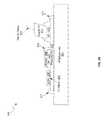
- FIG. 2Ais a schematic illustrating an exemplary hybrid integration photonic transceiver, in accordance with an embodiment of the invention.
- a hybrid integration photonic transceiver 200comprising a printed circuit board (PCB)/substrate 201 , a photonic CMOS die 203 , an electronic CMOS die 205 , metal interconnects 207 , an optical source module 209 , an optical input/output (I/O) 211 , wire bonds 213 , optical epoxy 215 , and optical fibers 217 .
- PCBprinted circuit board
- I/Ooptical input/output
- the PCB/substrate 201may comprise a support structure for the transceiver 200 , and may comprise both insulating and conductive material for isolating devices as well as providing electrical contact for active devices on the photonics die 203 as well as to devices on the electronics die 205 via the photonics die 203 .
- the PCB/substratemay provide a thermally conductive path to carry away heat generated by devices and circuits in the electronics die 205 and the optical source module 209 .
- the photonics die 203may comprise a silicon chip with active and passive optical devices such as waveguides, modulators, photodetectors, grating couplers, taps, and combiners, for example.
- the photonics die 203may also comprise metal interconnects 207 for coupling the electronics die 205 to the photonics die 203 , as well as grating couplers for coupling light into the die from the optical source module 209 and into/out of the die via the optical I/O 211 .
- the photonics die 203may comprise through-substrate-vias (TSVs), not shown, for electrical interconnection through the die, such as between the PCB/substrate 201 and the electronics die 205 .
- TSVsthrough-substrate-vias
- Optical interfacesmay also be facilitated by the optical epoxy 215 , providing both optical transparency and mechanical fixation.
- the electronics die 205may comprise a chip that provides all the required electronic functions of the photonic transceiver 200 .
- the electronics die 205may comprise a single chip or a plurality of die coupled to the photonics chip 203 via the metal interconnects 207 .
- the electronics die 205may comprise TIA's, LNAs, and control circuits for processing optical signals in the photonics chip 203 .
- the electronics die 205may comprise driver circuitry for controlling optical modulators in the photonics die 203 and variable gain amplifiers for amplifying electrical signals received from photodetectors in the photonics die 203 .
- the metal interconnects 207may comprise linear or 2D arrays of metal pillars, for example, to provide electrical contact between the photonics die 203 and the electronics die 205 .
- the metal interconnects 207may comprise copper pillars, or any other suitable metal for semiconductor contacts, such as stud bumps or solder bumps. Accordingly, the metal interconnects 207 may provide electrical contact between photodetectors in the photonics die 203 and associated receiver circuitry in the electronics die 205 .
- the metal interconnects 207may provide mechanical coupling of the electronics and photonics die, and may be encapsulated with underfill to protect the metal and other surfaces.
- the optical source module 209may comprise an assembly with an optical source, such as a semiconductor laser, and associated optical elements to direct one or more optical signals into the photonics die 203 .
- an optical sourcesuch as a semiconductor laser
- An example of the optical source moduleis described in U.S. patent application Ser. No. 12/500,465 filed on Jul. 9, 2009, which is hereby incorporated in its entirety.
- the optical signal or signals from the optical source assembly 209may be coupled into the photonics die 203 via optical fibers affixed above grating couplers in the photonics die 203 .
- the optical I/O 211may comprise an assembly for coupling the optical fibers 217 to the photonics die 203 . Accordingly, the optical I/O 211 may comprise mechanical support for one or more optical fibers and an optical surface to be coupled to the photonics die 203 , such as by the optical epoxy 215 .
- continuous-wave (CW) optical signalsmay be communicated into the photonics die 203 from the optical source module 209 via one or more grating couplers in the photonics die 203 .
- Photonic devices in the photonics die 203may then process the received optical signal.
- one or more optical modulatorsmay modulate the CW signal based on electrical signals received from the electronics die 205 .
- Electrical signalsmay be received from the electronics die 205 via the metal interconnects 207 .
- signal path lengthsmay be minimized, resulting in very high speed performance. For example, utilizing metal pillars with ⁇ 20 fF capacitance, speeds of 50 GHz and higher can be achieved.
- the modulated optical signalsmay then be communicated out of the photonics die 203 via grating couplers situated beneath the optical I/O 211 .
- high-speed electrical signals generated in the electronics die 205may be utilized to modulate a CW optical signal and subsequently communicated out of the photonics die 203 via the optical fibers 217 .
- modulated optical signalsmay be received in the photonics die 203 via the optical fibers 217 and the optical I/O 211 .
- the received optical signalsmay be communicated within the photonics die 203 via optical waveguides to one or more photodetectors integrated in the photonics die 203 .
- the photodetectorsmay be integrated in the photonics die 203 such that they lie directly beneath the associated receiver electronics circuitry in the electronics die 205 when bonded and electrically coupled by the low parasitic capacitance metal interconnects 207 .
- CMOScomplementary metal-oxide-semiconductor
- Bi-CMOScomplementary metal-oxide-semiconductor
- Si—Gestandard semiconductor processes
- integrating separate photonic and electronic dieenables the independent optimization of the performance of electronic and photonic functions within the respective semiconductor processes.
- FIG. 2Bis a perspective view of a hybrid integration photonic transceiver, in accordance with an embodiment of the invention. Referring to FIG. 2B , there is shown the PCB/substrate 201 , the photonics die 203 , electronics die 205 , the metal interconnects 207 , the optical source assembly 209 , and wire bonds 213 .
- the electronics die 205are shown prior to bonding to the surface of the photonics die 203 via the metal interconnects 207 , as illustrated by the dashed arrows below each die. While two electronics die 205 are shown in FIG. 2B , it should be noted that the invention is not so limited. Accordingly, any number of electronics die may be coupled to the photonics die 203 depending on number of transceivers, the particular semiconductor process node utilized, thermal conductance, and space limitations, for example.
- electronic functionsmay be integrated into the electronics die 205 and photonics circuitry may be integrated into the photonics die 203 utilizing independent semiconductor processes.
- the electronics die 205may comprise electronic devices associated with photonic devices in the photonics die 203 , thereby minimizing electrical path lengths while still allowing independent performance optimization of electronic and photonic devices.
- a CMOS processthat results in the highest electronics performance, such as the fastest switching speed, may not be optimum for photonics performance.
- different technologiesmay be incorporated in the different die. For example, SiGe processes may be used for photonic devices such as photodetectors, and 32 nm CMOS process, or even a SiGe or Bi-CMOS process, may be used for electronic devices on the electronics die 205 .
- the photonics die 203may comprise photonic circuits, whereby optical signals may be received, processed, and transmitted out of the photonics die 203 .
- the optical source assembly 209may provide a CW optical signal to the photonics die 203 , with the photonics circuitry in the photonics die 203 processing the CW signal.
- the CW signalmay be coupled into the photonics die 203 via grating couplers, communicated to various locations on the die via optical waveguides, modulated by Mach-Zehnder interferometer (MZI) modulators, and communicated out of the photonics die 203 into optical fibers.
- MZIMach-Zehnder interferometer
- FIG. 2Cis a perspective view of a hybrid integration photonic transceiver, in accordance with an embodiment of the invention. Referring to FIG. 2C , there is shown the PCB/substrate 201 , the photonics die 203 , electronics die 205 , the optical source assembly 209 , the optical I/O 211 , wire bonds 213 , and optical fibers 217 .
- the electronics die 205are shown bonded to the surface of the photonics die 203 via metal pillars. While two electronics die 205 are shown in FIG. 2C , it should again be noted that the invention is not so limited. Accordingly, any number of electronics die may be coupled to the photonics die 203 depending on number of transceivers, the particular CMOS node utilized, and space limitations, for example.
- electronic functionsmay be integrated into the electronics die 205 and photonics circuitry may be integrated into the photonics die 203 utilizing independent semiconductor processes.
- the electronics die 205may comprise electronic devices associated with photonic devices in the photonics die 203 , thereby minimizing electrical path lengths while still allowing independent performance optimization of electronic and photonic devices.
- Different technologiesmay be incorporated in the different die. For example, a Ge selective epitaxy process may be used for photodetectors in the photonics die 203 , and a 32 nm CMOS process may be used for electronic devices on the electronics die 205 .
- the photonics die 203may comprise photonic circuits, whereby optical signals may be received, processed, and transmitted out of the photonics die 203 .
- the optical source assembly 209may provide a CW optical signal to the photonics die 203 and biased by voltages coupled to the optical source assembly 209 via wire bonds 213 .
- Photonics circuitry in the photonics die 203may then process the CW signal.
- the CW signalmay be coupled into the photonics die 203 via grating couplers, communicated to various locations on the die via optical waveguides, modulated by MZI modulators, and communicated out of the photonics die 203 into the optical fibers 217 via the optical I/O 211 .
- Heatmay be conducted away from the die via the PCB/substrate 201 . In this manner, the hybrid integration of a plurality of high performance optical transceivers is enabled in standard semiconductor processes.
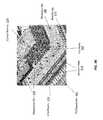
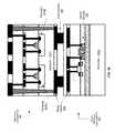
- FIG. 3is a schematic illustrating the hybrid integration of an electronics die to a photonics die, in accordance with an embodiment of the invention.
- an electronics die 205there is shown an electronics die 205 , metal interconnects 207 , and a photonics die/interposer 300 .
- the photonics die/interposer 300may comprise grating couplers 301 , a polarization splitting grating coupler 303 , a photodetector 305 , an optical modulator 307 , TSVs 309 , and optical waveguides 311 .
- the metal interconnects 207provide both electrical and mechanical coupling between the electronics die 205 and the photonics die/interposer 300 .
- the grating couplers 301provide for the coupling of light into and/or out of the photonics die/interposer 300 .
- the polarization-splitting grating coupler 303may enable the coupling of two polarizations of light into and/or out of the photonics die/interposer 300 .
- the modulator 307may comprise a MZI modulator, for example, and may be operable to modulate an optical signal based on electrical signals received from the electronics die 205 via the metal interconnects 207 .
- a CW optical signalmay be received from an optical source via one of the grating couplers 301 , communicated via the optical waveguides 311 , modulated by the optical modulator 307 , communicated back by the optical waveguides 311 , and out of the photonics die/interposer 300 via the other grating coupler 301 .
- the photodetector 305may comprise a semiconductor photodiode, for example, and may be operable to convert a received optical signal to an electrical signal.
- optical signals with perpendicular polarizationsmay be received by the polarization-splitting grating coupler 303 , communicated via the waveguides 311 , converted to an electrical signal by the photodetector 305 , with the resulting electrical signals communicated to the electronics die 205 via the metal interconnects 207 .
- the electrical signalsmay be further processed by electronics in the electronics die 205 and/or communicated to other circuitry via wire bonds or the metal interconnects 207 and the TSVs 309 .
- the photonics die/interposer 300comprises a silicon photonics die that may provide photonic circuits for a plurality of electronics die, thereby reducing or eliminating electrical interconnects between high-speed electronics. This may be utilized for high-speed memory access, high-speed processor interconnects, and coupling a plurality of high-speed electronics chips, for example.
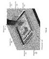
- FIG. 4Ais a schematic illustrating a cross-section of exemplary metal interconnect-coupled electrical and optoelectronic devices, in accordance with an embodiment of the invention.
- a hybrid integrated semiconductor structure 400comprising a silicon photonics substrate/chip/die 450 , an electronics substrate/chip/die 460 , and a metal layer 427 for substrate/chip physical and electrical coupling.
- the silicon photonics substrate/chip/die 450comprises optical devices 420 and associated layers
- the electronics substrate/chip/die 460comprises transistors 410 A and 410 B and associated layers.
- the layers of the dieare utilized to fabricate the transistors 410 A and 410 B and the optical devices 420 , to isolate, and to provide electrical connection to the devices, for example.
- the silicon photonics substrate/chip/die 450comprises a substrate 401 A, a buried oxide 403 , a Si-layer 405 , a contact layer 415 A, a metal 1 layer 417 A, and through-silicon vias (TSVs) 443 A and 443 B.
- the optical devices 420comprise doped and/or undoped regions of the Si-layer 405 , a salicide block 413 , doped contact regions 435 and 437 , etched region 439 , and the Ge-layer 445 .
- the salicide block 413comprises a layer of material to prevent the silicon of the optical devices 420 and other optical devices from being salicided during a standard CMOS process. If silicon in the optical devices was salicided, large optical losses would result.
- the salicide block 413blocks unwanted implants into the waveguides and other optical devices, which would also cause unwanted loss.
- the salicide block 413may be etched to the Si-layer 405 so that the Ge-layer 445 may be deposited.
- the Ge-layer 445may be utilized in a photodetector device, for example.
- etched regions 439 in the Si-layer 405may be utilized for optical confinement.
- the etch regions 439may be refilled with a low-k dielectric, for example, or may comprise an air gap with no refill material.
- Fill materialmay comprise silicon oxide or oxynitride materials, for example.
- the silicon electronics substrate/chip/die 460comprises a silicon substrate 401 B, a well 407 , a contact layer 415 B, a metal 1 layer 417 B, a last metal layer 423 , a passivation layer 425 , and the metal layer 427 .
- the metal 1 layer 417 B, the last metal layer 423 , and the metal layer 427provide electrical contact between layers and to electrical and optoelectronics devices, such as the transistors 410 A and 410 B and the optical devices 420 .
- the contact layer 415also enables electrical contact to the devices while providing electrical isolation between devices by incorporating insulating materials between conductive vias.
- the transistor 410 A and 410 Bcomprises a bulk transistor with source and drain regions formed in the well 407 or the substrate 401 B, respectively, from dopant implant processes, for example, as well as a gate 431 , and a passivation layer 433 .
- the gate 431may comprise metal or polysilicon, for example, and may be isolated from the well 407 by a thin oxide layer (not shown).
- separate semiconductor processesmay be utilized to fabricate the silicon photonics substrate/chip/die 450 and the electronics substrate/chip/die 460 so that the processes may be optimized for each type of device.
- the separate semiconductor processesmay comprise different CMOS nodes, or may comprise different technologies entirely, such as CMOS and SiGe.
- the wafers, or alternatively diced chips,may then be bonded together to form an optoelectronic hybrid module utilizing metal layers such as metal pillars.
- layer thicknesses and doping levelsmay be configured for the best electronic and photonic performance in the respective structure without the tradeoffs in performance associated with fabricating electronic and photonic structures concurrently.
- FIG. 4Bis a schematic of an alternative face-to-face coupling of electronic and photonic chips, in accordance with an embodiment of the invention.
- the silicon photonics chip 450 and the electronics chip 460coupled utilizing an interconnect layer 427 , which may comprise metal pillars, stud bumps, or solder bumps, for example.
- the silicon photonics chip 450may comprise a substrate 401 C, optical devices 420 , and metal layers 430 .
- the electronics chip 460may comprise a substrate 401 D, transistors 410 C and 410 D, and the metal layers 430 . Each of these elements may be similar to the like-named elements of FIG. 4A .
- FIG. 4Bmay be similar to that shown in FIG. 4A , but with the electronics and photonics chips bonded face-to-face, thereby removing the need for through-substrate-vias (TSVs).
- TSVsthrough-substrate-vias
- FIG. 4Cis a schematic of an alternative coupling of electronic and photonic chips, in accordance with an embodiment of the invention. Referring to FIG. 4C , there is shown the silicon photonics chip 450 and the electronics chip 460 coupled utilizing an interconnects 427 , which may comprise metal pillars, stud bumps, or solder bumps, for example.
- an interconnects 427which may comprise metal pillars, stud bumps, or solder bumps, for example.
- the silicon photonics chip 450may comprise a substrate 401 E, optical devices 420 , and metal layers 430 .
- the electronics chip 460may comprise a substrate 401 F, transistors 410 C and 410 D, and the metal layers 430 . Each of these elements may be similar to the like-named elements of FIGS. 4A and 4B .
- FIG. 4Cmay be similar to that shown in FIG. 4A , but with the silicon photonics chip 450 on bottom and the electronics chip 460 on top.
- the electrical contactsmay be made utilizing TSVs and metal interconnects, such as metal pillars or bumps.
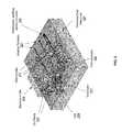
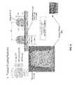
- FIG. 5is a diagram illustrating exemplary metal interconnects for coupling electrical and photonics die, in accordance with an embodiment of the invention.
- the exemplary copper pillars showncomprise widths on the order of 50 microns, but smaller diameters may be utilized for reduced parasitic capacitance.
- a tin/silver cap layermay be utilized for mechanical bonding and electrical contact, i.e. soldering.
- the dimensions of the metal interconnectsmay be adjusted based on speed requirements, device density, thermal properties, and capacitance and electrical resistance requirements, for example.
- a method and systemare disclosed for hybrid integration of optical communication systems.
- the one or more received CW optical signalsmay be processed based on electrical signals received from one or more electronics die 205 bonded to the silicon photonics die 203 / 300 via metal interconnects 207 .
- Modulated optical signalsmay be received in the photonics die 203 / 300 from one or more optical fibers 217 coupled to the silicon photonics die 203 / 300 .
- Electrical signalsmay be generated in the silicon photonics die 203 / 300 based on the received modulated optical signals and communicated to the one or more electronics die 205 via the metal interconnects 207 .
- the metal interconnects 207may comprise copper pillars, for example.
- the one or more CW optical signalsmay be received from an optical source assembly 209 coupled to the silicon photonics die 203 / 300 and/or from one or more optical fibers 217 coupled to the silicon photonics die 203 / 300 .
- the one or more received CW optical signalsmay be processed utilizing one or more optical modulators 105 A- 105 D/ 307 , which may comprise Mach-Zehnder interferometer modulators, for example.
- the electrical signalsmay be generated in the silicon photonics die 203 / 300 utilizing one or more photodetectors 111 A- 111 D/ 305 integrated in the silicon photonics die 203 / 300 .
- the optical signalsmay be communicated into and/or out of the silicon photonics die 203 / 300 utilizing grating couplers 117 A- 117 H/ 301 / 303 .
- the optical source 209may comprise one or more semiconductor lasers 101 .
- the hybrid integration optical communication system 100may comprise a plurality of transceivers 105 / 112 / 117 / 107 / 111 (A-F).
Landscapes
- Physics & Mathematics (AREA)
- General Physics & Mathematics (AREA)
- Optics & Photonics (AREA)
- Engineering & Computer Science (AREA)
- Nonlinear Science (AREA)
- Microelectronics & Electronic Packaging (AREA)
- Electromagnetism (AREA)
- Power Engineering (AREA)
- Computing Systems (AREA)
- Signal Processing (AREA)
- Computer Networks & Wireless Communication (AREA)
- Condensed Matter Physics & Semiconductors (AREA)
- Computer Hardware Design (AREA)
- Optical Modulation, Optical Deflection, Nonlinear Optics, Optical Demodulation, Optical Logic Elements (AREA)
- Optical Couplings Of Light Guides (AREA)
Abstract
Description
- This application is a continuation-in-part of U.S. application Ser. No. 12/554,449 filed on Sep. 4, 2009. This application also makes reference to U.S. application Ser. No. 13/422,776, filed on Mar. 6, 2012.
- Each of the above cited references is hereby incorporated by reference in its entirety.
- Certain embodiments of the invention relate to semiconductor processing. More specifically, certain embodiments of the invention relate to a method and system for hybrid integration of optical communication systems.
- As data networks scale to meet ever-increasing bandwidth requirements, the shortcomings of copper data channels are becoming apparent. Signal attenuation and crosstalk due to radiated electromagnetic energy are the main impediments encountered by designers of such systems. They can be mitigated to some extent with equalization, coding, and shielding, but these techniques require considerable power, complexity, and cable bulk penalties while offering only modest improvements in reach and very limited scalability. Free of such channel limitations, optical communication has been recognized as the successor to copper links.
- Further limitations and disadvantages of conventional and traditional approaches will become apparent to one of skill in the art, through comparison of such systems with the present invention as set forth in the remainder of the present application with reference to the drawings.
- A system and/or method for hybrid integration of optical communication systems, substantially as shown in and/or described in connection with at least one of the figures, as set forth more completely in the claims.
- Various advantages, aspects and novel features of the present invention, as well as details of an illustrated embodiment thereof, will be more fully understood from the following description and drawings.
FIG. 1 is a block diagram of a photonic transceiver, in accordance with an embodiment of the invention.FIG. 2A is a schematic illustrating an exemplary hybrid integration photonic transceiver, in accordance with an embodiment of the invention.FIG. 2B is a perspective view of a hybrid integration photonic transceiver, in accordance with an embodiment of the invention.FIG. 2C is a perspective view of a hybrid integration photonic transceiver, in accordance with an embodiment of the invention.FIG. 3 is a schematic illustrating the hybrid integration of an electronics die to a photonics die, in accordance with an embodiment of the invention.FIG. 4A is a schematic illustrating a cross-section of exemplary metal interconnect-coupled electrical and optoelectronic devices, in accordance with an embodiment of the invention.FIG. 4B is a schematic of an alternative face-to-face coupling of electronic and photonic chips, in accordance with an embodiment of the invention.FIG. 4C is a schematic of an alternative coupling of electronic and photonic chips, in accordance with an embodiment of the invention.FIG. 5 is a diagram illustrating exemplary metal pillars for coupling electrical and photonics die, in accordance with an embodiment of the invention.- Certain aspects of the invention may be found in a method and system for hybrid integration of optical communication systems. Exemplary aspects of the invention may comprise receiving one or more continuous wave (CW) optical signals in a silicon photonics die from an optical source external to the photonics die. The one or more received CW optical signals may be processed based on electrical signals received from one or more electronics die bonded to the silicon photonics die via metal interconnects, which may comprise copper pillars, for example. Modulated optical signals may be received in the silicon photonics die from one or more optical fibers coupled to the silicon photonics die. Electrical signals may be generated in the silicon photonics die based on the received modulated optical signals and communicated to the one or more electronics die via the metal interconnects. The metal interconnects may comprise copper pillars. The one or more CW optical signals may be received from an optical source assembly coupled to the silicon photonics die and/or from one or more optical fibers coupled to the silicon photonics die. The one or more received CW optical signals may be processed utilizing one or more optical modulators, which may comprise Mach-Zehnder interferometer modulators. The electrical signals may be generated in the silicon photonics die utilizing one or more photodetectors integrated in the silicon photonics die. The optical signals may be communicated into and/or out of the silicon photonics die utilizing grating couplers. The optical source may comprise one or more semiconductor lasers. The hybrid integration optical communication system may comprise a plurality of transceivers.
FIG. 1 is a block diagram of a photonic transceiver, in accordance with an embodiment of the invention. Referring toFIG. 1 , there is shown optoelectronic devices in atransceiver 100 comprising high speedoptical modulators 105A-105D, high-speed photodiodes111A-111D,monitor photodiodes 113A-113H, and opticaldevices comprising taps 103A-103K,optical terminations 115A-115D, andgrating couplers 117A-117H. There are also shown electrical devices and circuits comprising transimpedance and limiting amplifiers (TIA/LAs)107A-107E, analog and digital control circuits109, andcontrol sections 112A-112D. Optical signals are communicated between optical and optoelectronic devices via optical waveguides fabricated in a photonics chip. Additionally, optical waveguides are indicated inFIG. 1 by the dashed ovals.- The high speed
optical modulators 105A-105D comprise Mach-Zehnder or ring modulators, for example, and enable the modulation of the CW laser input signal. The high speedoptical modulators 105A-105D are controlled by thecontrol sections 112A-112D, and the outputs of the modulators are optically coupled via waveguides to thegrating couplers 117E-117H. Exemplary modulation techniques comprise amplitude shift keying (ASK), binary phase shift keying (BPSK), pulse amplitude modulation (PAM), quadrature amplitude modulation (QAM), quadrature phase shift keying (QPSK), and dual polarization quadrature phase shift keying (DP-QPSK). Thetaps 103D-103K comprise four-port optical couplers, for example, and are utilized to sample the optical signals generated by the high speedoptical modulators 105A-105D, with the sampled signals being measured by themonitor photodiodes 113A-113H. The unused branches of thetaps 103D-103K are terminated byoptical terminations 115A-115D to avoid back reflections of unwanted signals. - The
grating couplers 117A-117H comprise optical gratings that enable coupling of light into and out of the chip. Thegrating couplers 117A-117D are utilized to couple light received from optical fibers into the chip, and may comprise polarization independent grating couplers. Thegrating couplers 117E-117H are utilized to couple light from the chip into optical fibers. The optical fibers may be epoxied, for example, to the chip, and may be aligned at an angle from normal to the surface of the chip to optimize coupling efficiency. - The high-speed photodiodes111A-111D convert optical signals received from the
grating couplers 117A-117D into electrical signals that are communicated to the TIA/LAs107A-107D for processing. The analog and digital control circuits109 may control gain levels or other parameters in the operation of the TIA/LAs107A-107D. The TIA/LAs107A-107D, the analog and digital control circuits109, and thecontrol sections 112A-112D may be integrated on an electronics chip that may be bonded to the silicon photonics chip via metal interconnects. In an exemplary scenario, the metal interconnects may comprise copper pillars. In this manner, electronic and photonic performance may be optimized independently on different fabrication technology platforms. In an exemplary scenario, the electronics die may comprise CMOS die, but the invention is not so limited. Accordingly, any semiconductor technology may be utilized to fabricate the electronic die, such as CMOS, Bi-COMS, SiGe, or III-V processes. The TIA/LAs107A-107D may then communicate electrical signals to other circuitry on the electronics chip. - The TIA/LAs107A-107D may comprise narrowband, non-linear optoelectronic receiver circuitry. Accordingly, the narrowband receiver front-end may be followed by a restorer circuit, such as, for example, a non-return to zero (NRZ) level restorer circuit. A restorer circuit limits the bandwidth of the optical receiver in order to decrease the integrated noise, thereby increasing the signal to noise ratio. An NRZ level restorer may be used to convert the resulting data pulses back into NRZ data.
- The
control sections 112A-112D comprise electronic circuitry that enable modulation of the CW laser signal received from thetaps 103A-103C. The high speedoptical modulators 105A-105D require high-speed electrical signals to modulate the refractive index in respective branches of a Mach-Zehnder interferometer (MZI), for example. - In an embodiment of the invention, the integration of all optical and optoelectronic devices required for a transceiver into a single silicon photonics chip, and of all required electronic devices on one or more electronics chips, enables optimized performance of the resulting single hybrid package. In this manner, electronic device performance may be optimized independently of the optimization of photonic devices in the silicon photonic chip. For example, the electronics chip may be optimized on a 32 nm CMOS process, while the photonics chip may be optimized on a 130 nm CMOS node. Additionally, the electronics or photonics chips may be fabricated utilizing technologies other than CMOS, such as SiGe or bipolar-CMOS (Bi-CMOS). The electronics devices may be placed on the electronics chip such that they are located directly above their associated photonics devices when bonded to the photonics chip. For example, the
control sections 112A-112D may be located on the electronics chip such that they lie directly above the high-speedoptical modulators 105A-105B and can be coupled by low parasitic copper pillars. - In an exemplary embodiment, the
hybrid transceiver 100 comprises four optoelectronic transceivers with one optical source, and enables communication of optical signals vertically to and from the surface of the photonics chip, thereby enabling in an exemplary embodiment, the use of CMOS processes and structures, including a CMOS guard ring. The photonics chip may comprise both active devices, such as photodetectors and modulators, and passive devices, such as waveguides, splitters, combiners, and grating couplers, thereby enabling photonic circuits to be integrated on silicon chips. FIG. 2A is a schematic illustrating an exemplary hybrid integration photonic transceiver, in accordance with an embodiment of the invention. Referring toFIG. 2A , there is shown a hybridintegration photonic transceiver 200 comprising a printed circuit board (PCB)/substrate 201, a photonic CMOS die203, an electronic CMOS die205, metal interconnects207, anoptical source module 209, an optical input/output (I/O)211,wire bonds 213,optical epoxy 215, andoptical fibers 217.- The PCB/
substrate 201 may comprise a support structure for thetransceiver 200, and may comprise both insulating and conductive material for isolating devices as well as providing electrical contact for active devices on the photonics die203 as well as to devices on the electronics die205 via the photonics die203. In addition, the PCB/substrate may provide a thermally conductive path to carry away heat generated by devices and circuits in the electronics die205 and theoptical source module 209. - The photonics die203 may comprise a silicon chip with active and passive optical devices such as waveguides, modulators, photodetectors, grating couplers, taps, and combiners, for example. The photonics die203 may also comprise
metal interconnects 207 for coupling the electronics die205 to the photonics die203, as well as grating couplers for coupling light into the die from theoptical source module 209 and into/out of the die via the optical I/O 211. In addition, the photonics die203 may comprise through-substrate-vias (TSVs), not shown, for electrical interconnection through the die, such as between the PCB/substrate 201 and the electronics die205. Optical interfaces may also be facilitated by theoptical epoxy 215, providing both optical transparency and mechanical fixation. - The electronics die205 may comprise a chip that provides all the required electronic functions of the
photonic transceiver 200. The electronics die205 may comprise a single chip or a plurality of die coupled to thephotonics chip 203 via the metal interconnects207. The electronics die205 may comprise TIA's, LNAs, and control circuits for processing optical signals in thephotonics chip 203. For example, the electronics die205 may comprise driver circuitry for controlling optical modulators in the photonics die203 and variable gain amplifiers for amplifying electrical signals received from photodetectors in the photonics die203. By incorporating photonics devices in the photonics die203 and electronic devices in the electronics die205, the processes for each chip may be optimized for the type of devices incorporated. - The metal interconnects207 may comprise linear or 2D arrays of metal pillars, for example, to provide electrical contact between the photonics die203 and the electronics die205. In an exemplary scenario, the metal interconnects207 may comprise copper pillars, or any other suitable metal for semiconductor contacts, such as stud bumps or solder bumps. Accordingly, the metal interconnects207 may provide electrical contact between photodetectors in the photonics die203 and associated receiver circuitry in the electronics die205. In addition, the metal interconnects207 may provide mechanical coupling of the electronics and photonics die, and may be encapsulated with underfill to protect the metal and other surfaces.
- The
optical source module 209 may comprise an assembly with an optical source, such as a semiconductor laser, and associated optical elements to direct one or more optical signals into the photonics die203. An example of the optical source module is described in U.S. patent application Ser. No. 12/500,465 filed on Jul. 9, 2009, which is hereby incorporated in its entirety. In another exemplary scenario, the optical signal or signals from theoptical source assembly 209 may be coupled into the photonics die203 via optical fibers affixed above grating couplers in the photonics die203. - The optical I/
O 211 may comprise an assembly for coupling theoptical fibers 217 to the photonics die203. Accordingly, the optical I/O 211 may comprise mechanical support for one or more optical fibers and an optical surface to be coupled to the photonics die203, such as by theoptical epoxy 215. - In operation, continuous-wave (CW) optical signals may be communicated into the photonics die203 from the
optical source module 209 via one or more grating couplers in the photonics die203. Photonic devices in the photonics die203 may then process the received optical signal. For example, one or more optical modulators may modulate the CW signal based on electrical signals received from the electronics die205. Electrical signals may be received from the electronics die205 via the metal interconnects207. By integrating modulators in the photonics die203 directly beneath the source of the electrical signals in the electronics die205, signal path lengths may be minimized, resulting in very high speed performance. For example, utilizing metal pillars with <20 fF capacitance, speeds of 50 GHz and higher can be achieved. - The modulated optical signals may then be communicated out of the photonics die203 via grating couplers situated beneath the optical I/
O 211. In this manner, high-speed electrical signals generated in the electronics die205 may be utilized to modulate a CW optical signal and subsequently communicated out of the photonics die203 via theoptical fibers 217. - Similarly, modulated optical signals may be received in the photonics die203 via the
optical fibers 217 and the optical I/O 211. The received optical signals may be communicated within the photonics die203 via optical waveguides to one or more photodetectors integrated in the photonics die203. The photodetectors may be integrated in the photonics die203 such that they lie directly beneath the associated receiver electronics circuitry in the electronics die205 when bonded and electrically coupled by the low parasitic capacitance metal interconnects207. - The hybrid integration of electronics die on photonic die via metal interconnects enables very high speed optical transceivers utilizing standard semiconductor processes, such as CMOS, Bi-CMOS, or Si—Ge. In addition, integrating separate photonic and electronic die enables the independent optimization of the performance of electronic and photonic functions within the respective semiconductor processes.
FIG. 2B is a perspective view of a hybrid integration photonic transceiver, in accordance with an embodiment of the invention. Referring toFIG. 2B , there is shown the PCB/substrate 201, the photonics die203, electronics die205, the metal interconnects207, theoptical source assembly 209, andwire bonds 213.- The electronics die205 are shown prior to bonding to the surface of the photonics die203 via the metal interconnects207, as illustrated by the dashed arrows below each die. While two electronics die205 are shown in
FIG. 2B , it should be noted that the invention is not so limited. Accordingly, any number of electronics die may be coupled to the photonics die203 depending on number of transceivers, the particular semiconductor process node utilized, thermal conductance, and space limitations, for example. - In an exemplary embodiment, electronic functions may be integrated into the electronics die205 and photonics circuitry may be integrated into the photonics die203 utilizing independent semiconductor processes. The electronics die205 may comprise electronic devices associated with photonic devices in the photonics die203, thereby minimizing electrical path lengths while still allowing independent performance optimization of electronic and photonic devices. For example, a CMOS process that results in the highest electronics performance, such as the fastest switching speed, may not be optimum for photonics performance. Similarly, different technologies may be incorporated in the different die. For example, SiGe processes may be used for photonic devices such as photodetectors, and 32 nm CMOS process, or even a SiGe or Bi-CMOS process, may be used for electronic devices on the electronics die205.
- The photonics die203 may comprise photonic circuits, whereby optical signals may be received, processed, and transmitted out of the photonics die203. The
optical source assembly 209 may provide a CW optical signal to the photonics die203, with the photonics circuitry in the photonics die203 processing the CW signal. For example, the CW signal may be coupled into the photonics die203 via grating couplers, communicated to various locations on the die via optical waveguides, modulated by Mach-Zehnder interferometer (MZI) modulators, and communicated out of the photonics die203 into optical fibers. In this manner, the hybrid integration of a plurality of high performance optical transceivers is enabled in semiconductor processes. FIG. 2C is a perspective view of a hybrid integration photonic transceiver, in accordance with an embodiment of the invention. Referring toFIG. 2C , there is shown the PCB/substrate 201, the photonics die203, electronics die205, theoptical source assembly 209, the optical I/O 211,wire bonds 213, andoptical fibers 217.- The electronics die205 are shown bonded to the surface of the photonics die203 via metal pillars. While two electronics die205 are shown in
FIG. 2C , it should again be noted that the invention is not so limited. Accordingly, any number of electronics die may be coupled to the photonics die203 depending on number of transceivers, the particular CMOS node utilized, and space limitations, for example. - In an exemplary embodiment, electronic functions may be integrated into the electronics die205 and photonics circuitry may be integrated into the photonics die203 utilizing independent semiconductor processes. The electronics die205 may comprise electronic devices associated with photonic devices in the photonics die203, thereby minimizing electrical path lengths while still allowing independent performance optimization of electronic and photonic devices. Different technologies may be incorporated in the different die. For example, a Ge selective epitaxy process may be used for photodetectors in the photonics die203, and a 32 nm CMOS process may be used for electronic devices on the electronics die205.
- The photonics die203 may comprise photonic circuits, whereby optical signals may be received, processed, and transmitted out of the photonics die203. The
optical source assembly 209 may provide a CW optical signal to the photonics die203 and biased by voltages coupled to theoptical source assembly 209 via wire bonds213. Photonics circuitry in the photonics die203 may then process the CW signal. For example, the CW signal may be coupled into the photonics die203 via grating couplers, communicated to various locations on the die via optical waveguides, modulated by MZI modulators, and communicated out of the photonics die203 into theoptical fibers 217 via the optical I/O 211. Heat may be conducted away from the die via the PCB/substrate 201. In this manner, the hybrid integration of a plurality of high performance optical transceivers is enabled in standard semiconductor processes. FIG. 3 is a schematic illustrating the hybrid integration of an electronics die to a photonics die, in accordance with an embodiment of the invention. Referring toFIG. 3 , there is shown an electronics die205, metal interconnects207, and a photonics die/interposer 300. The photonics die/interposer 300 may comprisegrating couplers 301, a polarization splittinggrating coupler 303, aphotodetector 305, anoptical modulator 307,TSVs 309, andoptical waveguides 311.- The metal interconnects207 provide both electrical and mechanical coupling between the electronics die205 and the photonics die/
interposer 300. Thegrating couplers 301 provide for the coupling of light into and/or out of the photonics die/interposer 300. Similarly, the polarization-splittinggrating coupler 303 may enable the coupling of two polarizations of light into and/or out of the photonics die/interposer 300. - The
modulator 307 may comprise a MZI modulator, for example, and may be operable to modulate an optical signal based on electrical signals received from the electronics die205 via the metal interconnects207. In an exemplary scenario, a CW optical signal may be received from an optical source via one of thegrating couplers 301, communicated via theoptical waveguides 311, modulated by theoptical modulator 307, communicated back by theoptical waveguides 311, and out of the photonics die/interposer 300 via the othergrating coupler 301. - The
photodetector 305 may comprise a semiconductor photodiode, for example, and may be operable to convert a received optical signal to an electrical signal. In an exemplary scenario, optical signals with perpendicular polarizations may be received by the polarization-splittinggrating coupler 303, communicated via thewaveguides 311, converted to an electrical signal by thephotodetector 305, with the resulting electrical signals communicated to the electronics die205 via the metal interconnects207. The electrical signals may be further processed by electronics in the electronics die205 and/or communicated to other circuitry via wire bonds or the metal interconnects207 and theTSVs 309. - The photonics die/
interposer 300 comprises a silicon photonics die that may provide photonic circuits for a plurality of electronics die, thereby reducing or eliminating electrical interconnects between high-speed electronics. This may be utilized for high-speed memory access, high-speed processor interconnects, and coupling a plurality of high-speed electronics chips, for example. FIG. 4A is a schematic illustrating a cross-section of exemplary metal interconnect-coupled electrical and optoelectronic devices, in accordance with an embodiment of the invention. Referring toFIG. 4A , there is shown a hybridintegrated semiconductor structure 400 comprising a silicon photonics substrate/chip/die450, an electronics substrate/chip/die460, and ametal layer 427 for substrate/chip physical and electrical coupling. The silicon photonics substrate/chip/die450 comprisesoptical devices 420 and associated layers, and the electronics substrate/chip/die460 comprisestransistors transistors optical devices 420, to isolate, and to provide electrical connection to the devices, for example.- The silicon photonics substrate/chip/die450 comprises a
substrate 401A, a buriedoxide 403, a Si-layer 405, acontact layer 415A, ametal 1layer 417A, and through-silicon vias (TSVs)443A and443B. Theoptical devices 420 comprise doped and/or undoped regions of the Si-layer 405, asalicide block 413, dopedcontact regions region 439, and the Ge-layer 445. Thesalicide block 413 comprises a layer of material to prevent the silicon of theoptical devices 420 and other optical devices from being salicided during a standard CMOS process. If silicon in the optical devices was salicided, large optical losses would result. Additionally, the salicide block413 blocks unwanted implants into the waveguides and other optical devices, which would also cause unwanted loss. Thesalicide block 413 may be etched to the Si-layer 405 so that the Ge-layer 445 may be deposited. The Ge-layer 445 may be utilized in a photodetector device, for example. In addition, etchedregions 439 in the Si-layer 405 may be utilized for optical confinement. Theetch regions 439 may be refilled with a low-k dielectric, for example, or may comprise an air gap with no refill material. Fill material may comprise silicon oxide or oxynitride materials, for example. - The silicon electronics substrate/chip/die460 comprises a
silicon substrate 401B, a well407, acontact layer 415B, ametal 1layer 417B, alast metal layer 423, apassivation layer 425, and themetal layer 427. Themetal 1layer 417B, thelast metal layer 423, and themetal layer 427 provide electrical contact between layers and to electrical and optoelectronics devices, such as thetransistors optical devices 420. The contact layer415 also enables electrical contact to the devices while providing electrical isolation between devices by incorporating insulating materials between conductive vias. - The
transistor substrate 401B, respectively, from dopant implant processes, for example, as well as agate 431, and apassivation layer 433. Thegate 431 may comprise metal or polysilicon, for example, and may be isolated from the well407 by a thin oxide layer (not shown). - In an embodiment of the invention, separate semiconductor processes may be utilized to fabricate the silicon photonics substrate/chip/die450 and the electronics substrate/chip/die460 so that the processes may be optimized for each type of device. In an exemplary scenario, the separate semiconductor processes may comprise different CMOS nodes, or may comprise different technologies entirely, such as CMOS and SiGe.
- The wafers, or alternatively diced chips, may then be bonded together to form an optoelectronic hybrid module utilizing metal layers such as metal pillars. In this manner, layer thicknesses and doping levels may be configured for the best electronic and photonic performance in the respective structure without the tradeoffs in performance associated with fabricating electronic and photonic structures concurrently.
FIG. 4B is a schematic of an alternative face-to-face coupling of electronic and photonic chips, in accordance with an embodiment of the invention. Referring toFIG. 4B , there is shown thesilicon photonics chip 450 and theelectronics chip 460 coupled utilizing aninterconnect layer 427, which may comprise metal pillars, stud bumps, or solder bumps, for example.- The
silicon photonics chip 450 may comprise asubstrate 401C,optical devices 420, and metal layers430. Theelectronics chip 460 may comprise asubstrate 401D,transistors FIG. 4A . - The embodiment shown in
FIG. 4B may be similar to that shown inFIG. 4A , but with the electronics and photonics chips bonded face-to-face, thereby removing the need for through-substrate-vias (TSVs). FIG. 4C is a schematic of an alternative coupling of electronic and photonic chips, in accordance with an embodiment of the invention. Referring toFIG. 4C , there is shown thesilicon photonics chip 450 and theelectronics chip 460 coupled utilizing aninterconnects 427, which may comprise metal pillars, stud bumps, or solder bumps, for example.- The
silicon photonics chip 450 may comprise asubstrate 401E,optical devices 420, and metal layers430. Theelectronics chip 460 may comprise asubstrate 401F,transistors FIGS. 4A and 4B . - The embodiment shown in
FIG. 4C may be similar to that shown inFIG. 4A , but with thesilicon photonics chip 450 on bottom and theelectronics chip 460 on top. In this scenario, the electrical contacts may be made utilizing TSVs and metal interconnects, such as metal pillars or bumps. FIG. 5 is a diagram illustrating exemplary metal interconnects for coupling electrical and photonics die, in accordance with an embodiment of the invention. Referring toFIG. 5 , there is shown cross-section and perspective views of the metal interconnects207. The exemplary copper pillars shown comprise widths on the order of 50 microns, but smaller diameters may be utilized for reduced parasitic capacitance. In addition, a tin/silver cap layer may be utilized for mechanical bonding and electrical contact, i.e. soldering. The dimensions of the metal interconnects may be adjusted based on speed requirements, device density, thermal properties, and capacitance and electrical resistance requirements, for example.- In an embodiment of the invention, a method and system are disclosed for hybrid integration of optical communication systems. In this regard, receiving one or more continuous wave (CW) optical signals in a silicon photonics die203/300 from an
optical source 209 external to the silicon photonics die203/300. The one or more received CW optical signals may be processed based on electrical signals received from one or more electronics die205 bonded to the silicon photonics die203/300 via metal interconnects207. - Modulated optical signals may be received in the photonics die203/300 from one or more
optical fibers 217 coupled to the silicon photonics die203/300. Electrical signals may be generated in the silicon photonics die203/300 based on the received modulated optical signals and communicated to the one or more electronics die205 via the metal interconnects207. The metal interconnects207 may comprise copper pillars, for example. The one or more CW optical signals may be received from anoptical source assembly 209 coupled to the silicon photonics die203/300 and/or from one or moreoptical fibers 217 coupled to the silicon photonics die203/300. - The one or more received CW optical signals may be processed utilizing one or more
optical modulators 105A-105D/307, which may comprise Mach-Zehnder interferometer modulators, for example. The electrical signals may be generated in the silicon photonics die203/300 utilizing one or more photodetectors111A-111D/305 integrated in the silicon photonics die203/300. The optical signals may be communicated into and/or out of the silicon photonics die203/300 utilizinggrating couplers 117A-117H/301/303. Theoptical source 209 may comprise one ormore semiconductor lasers 101. The hybrid integrationoptical communication system 100 may comprise a plurality of transceivers105/112/117/107/111 (A-F). - While the invention has been described with reference to certain embodiments, it will be understood by those skilled in the art that various changes may be made and equivalents may be substituted without departing from the scope of the present invention. In addition, many modifications may be made to adapt a particular situation or material to the teachings of the present invention without departing from its scope. Therefore, it is intended that the present invention not be limited to the particular embodiments disclosed, but that the present invention will include all embodiments falling within the scope of the appended claims.
Claims (20)
Priority Applications (11)
| Application Number | Priority Date | Filing Date | Title |
|---|---|---|---|
| US13/568,406US9331096B2 (en) | 2009-09-04 | 2012-08-07 | Method and system for hybrid integration of optical communication systems |
| JP2013162549AJP2014035546A (en) | 2012-08-07 | 2013-08-05 | Method and system for hybrid integration of optical communication system |
| EP13179442.2AEP2696229A3 (en) | 2012-08-07 | 2013-08-06 | Method and system for hybrid integration of optical communication systems |
| CN201710932364.7ACN107608040B (en) | 2012-08-07 | 2013-08-07 | Method and system for communication |
| CN201310342196.8ACN103580751B (en) | 2012-08-07 | 2013-08-07 | Method and system for compound integration of optical communication systems |
| KR1020130093470AKR102105212B1 (en) | 2012-08-07 | 2013-08-07 | Method and system for hybrid integration of optical communication systems |
| TW106132561ATW201743577A (en) | 2012-08-07 | 2013-08-07 | Method and system for hybrid integration of optical communication systems |
| TW102128373ATWI604701B (en) | 2012-08-07 | 2013-08-07 | Method and system for hybrid integration of optical communication systems |
| US15/144,611US9625665B2 (en) | 2009-09-04 | 2016-05-02 | Method and system for hybrid integration of optical communication systems |
| US15/487,770US9829661B2 (en) | 2009-09-04 | 2017-04-14 | Method and system for hybrid integration of optical communication systems |
| US15/818,352US20180074270A1 (en) | 2009-09-04 | 2017-11-20 | Method And System For Hybrid Integration Of Optical Communication Systems |
Applications Claiming Priority (3)
| Application Number | Priority Date | Filing Date | Title |
|---|---|---|---|
| US12/554,449US8877616B2 (en) | 2008-09-08 | 2009-09-04 | Method and system for monolithic integration of photonics and electronics in CMOS processes |
| US13/422,776US8831437B2 (en) | 2009-09-04 | 2012-03-16 | Method and system for a photonic interposer |
| US13/568,406US9331096B2 (en) | 2009-09-04 | 2012-08-07 | Method and system for hybrid integration of optical communication systems |
Related Parent Applications (1)
| Application Number | Title | Priority Date | Filing Date |
|---|---|---|---|
| US12/554,449Continuation-In-PartUS8877616B2 (en) | 2008-09-08 | 2009-09-04 | Method and system for monolithic integration of photonics and electronics in CMOS processes |
Related Child Applications (1)
| Application Number | Title | Priority Date | Filing Date |
|---|---|---|---|
| US15/144,611ContinuationUS9625665B2 (en) | 2009-09-04 | 2016-05-02 | Method and system for hybrid integration of optical communication systems |
Publications (2)
| Publication Number | Publication Date |
|---|---|
| US20120301149A1true US20120301149A1 (en) | 2012-11-29 |
| US9331096B2 US9331096B2 (en) | 2016-05-03 |
Family
ID=47219302
Family Applications (4)
| Application Number | Title | Priority Date | Filing Date |
|---|---|---|---|
| US13/568,406ActiveUS9331096B2 (en) | 2009-09-04 | 2012-08-07 | Method and system for hybrid integration of optical communication systems |
| US15/144,611ActiveUS9625665B2 (en) | 2009-09-04 | 2016-05-02 | Method and system for hybrid integration of optical communication systems |
| US15/487,770ActiveUS9829661B2 (en) | 2009-09-04 | 2017-04-14 | Method and system for hybrid integration of optical communication systems |
| US15/818,352AbandonedUS20180074270A1 (en) | 2009-09-04 | 2017-11-20 | Method And System For Hybrid Integration Of Optical Communication Systems |
Family Applications After (3)
| Application Number | Title | Priority Date | Filing Date |
|---|---|---|---|
| US15/144,611ActiveUS9625665B2 (en) | 2009-09-04 | 2016-05-02 | Method and system for hybrid integration of optical communication systems |
| US15/487,770ActiveUS9829661B2 (en) | 2009-09-04 | 2017-04-14 | Method and system for hybrid integration of optical communication systems |
| US15/818,352AbandonedUS20180074270A1 (en) | 2009-09-04 | 2017-11-20 | Method And System For Hybrid Integration Of Optical Communication Systems |
Country Status (1)
| Country | Link |
|---|---|
| US (4) | US9331096B2 (en) |
Cited By (16)
| Publication number | Priority date | Publication date | Assignee | Title |
|---|---|---|---|---|
| US20120294608A1 (en)* | 2011-05-20 | 2012-11-22 | The Trustees Of Princeton University | System and method for broadband rf interference cancellation |
| US20150063745A1 (en)* | 2013-08-29 | 2015-03-05 | Industrial Technology Research Institute | Optical coupling module |
| US9203425B2 (en)* | 2007-06-13 | 2015-12-01 | Ramot At Tel-Aviv University Ltd. | Linearized optical digital-to-analog modulator |
| WO2016050243A1 (en)* | 2014-09-30 | 2016-04-07 | Technische Universität Berlin | Optoelectronic component |
| US9500821B2 (en) | 2014-10-27 | 2016-11-22 | Coriant Advanced Technology, LLC | Photonic interface for electronic circuit |
| US20170026123A1 (en)* | 2014-02-03 | 2017-01-26 | Luxtera, Inc. | Method And System For A Bi-Directional Multi-Wavelength Receiver For Standard Single-Mode fiber Based On Grating Couplers |
| US20170030743A1 (en)* | 2015-07-30 | 2017-02-02 | Dr. Johannes Heidenhain Gmbh | Position measuring device |
| US20170082801A1 (en)* | 2015-09-18 | 2017-03-23 | Luxtera, Inc. | Method And System For Partial Integration Of Wavelength Division Multiplexing And Bi-Directional Solutions |
| US20170237516A1 (en)* | 2015-11-18 | 2017-08-17 | Luxtera, Inc. | Method and System for Cassette Based Wavelength Division Multiplexing |
| US9874693B2 (en) | 2015-06-10 | 2018-01-23 | The Research Foundation For The State University Of New York | Method and structure for integrating photonics with CMOs |
| US10924269B1 (en)* | 2018-08-02 | 2021-02-16 | Inphi Corporation | Compact optical module integrated for communicating cryptocurrency transaction |
| US10976491B2 (en) | 2016-11-23 | 2021-04-13 | The Research Foundation For The State University Of New York | Photonics interposer optoelectronics |
| CN113759475A (en)* | 2020-06-05 | 2021-12-07 | 颖飞公司 | Inner packaging type photoelectric module |
| US20220336433A1 (en)* | 2019-09-11 | 2022-10-20 | Rockley Photonics Limited | Siliconized heterogeneous optical engine |
| US20220400548A1 (en)* | 2021-06-11 | 2022-12-15 | Intel Corporation | Flex-pcb integrated packaging for silicon photonics lidar |
| US11670627B1 (en)* | 2018-12-21 | 2023-06-06 | Psiquantum, Corp. | Hybrid system including photonic and electronic integrated circuits and cooling plate |
Families Citing this family (16)
| Publication number | Priority date | Publication date | Assignee | Title |
|---|---|---|---|---|
| US8831437B2 (en)* | 2009-09-04 | 2014-09-09 | Luxtera, Inc. | Method and system for a photonic interposer |
| US9577780B2 (en) | 2014-06-26 | 2017-02-21 | Luxtera, Inc. | Method and system for a polarization immune wavelength division multiplexing demultiplexer |
| US10027420B2 (en)* | 2014-06-26 | 2018-07-17 | Luxtera, Inc. | Method and system for a silicon-based optical phase modulator with high modal overlap |
| US10211970B2 (en)* | 2017-03-31 | 2019-02-19 | Intel Corporation | Millimeter wave CMOS engines for waveguide fabrics |
| US10267988B2 (en) | 2017-06-30 | 2019-04-23 | Taiwan Semiconductor Manufacturing Company, Ltd. | Photonic package and method forming same |
| US10594111B2 (en) | 2017-08-31 | 2020-03-17 | International Business Machines Corporation | Lateral current injection electro-optical device with well-separated doped III-V layers structured as photonic crystals |
| FR3074587B1 (en)* | 2017-12-06 | 2020-01-03 | Commissariat A L'energie Atomique Et Aux Energies Alternatives | PHOTONIC CHIP WITH OPTICAL PATH FOLDING AND INTEGRATED COLLIMATION STRUCTURE |
| US11828991B2 (en) | 2019-03-15 | 2023-11-28 | Hisense Broadband Multimedia Technologies Co., Ltd. | Optical module |
| US11493688B2 (en) | 2019-06-04 | 2022-11-08 | Electronicsand Telecommunications Research Institute | Optical module |
| US11300727B2 (en) | 2019-07-31 | 2022-04-12 | Advanced Semiconductor Engineering, Inc. | Optical communication package structure and method for manufacturing the same |
| KR102671347B1 (en)* | 2021-03-17 | 2024-06-03 | 오프로세서 인코퍼레이티드 | Optical Device Module Package |
| US11923269B2 (en) | 2021-04-07 | 2024-03-05 | International Business Machines Corporation | Co-packaged optical module |
| US12135454B2 (en) | 2021-04-16 | 2024-11-05 | Taiwan Semiconductor Manufacturing Co., Ltd. | Structure and process for photonic packages |
| US12429565B2 (en) | 2021-06-16 | 2025-09-30 | Apple Inc. | Single-chip optical transceiver |
| US11835777B2 (en) | 2022-03-18 | 2023-12-05 | Celestial Ai Inc. | Optical multi-die interconnect bridge (OMIB) |
| US12436346B2 (en) | 2022-03-18 | 2025-10-07 | Celestial Ai Inc. | Optically bridged multicomponent package with extended temperature range |
Citations (16)
| Publication number | Priority date | Publication date | Assignee | Title |
|---|---|---|---|---|
| US20030109142A1 (en)* | 2001-06-22 | 2003-06-12 | Cable James S. | Integrated photodetector for VCSEL feedback control |
| US20040241892A1 (en)* | 2003-05-30 | 2004-12-02 | International Business Machines Corporation | Integrated optical transducer assembly and method of forming the same |
| US20060008223A1 (en)* | 2003-08-15 | 2006-01-12 | Luxtera, Inc | PN diode optical modulators fabricated in rib waveguides |
| US20060038168A1 (en)* | 2001-05-21 | 2006-02-23 | Estes Michael J | Terahertz interconnect system and applications |
| US7027673B1 (en)* | 2002-06-19 | 2006-04-11 | Luxtera, Inc. | Integrated dual waveguides |
| US7162124B1 (en)* | 2003-03-14 | 2007-01-09 | Luxtera, Inc. | Fiber to chip coupler |
| US20080099928A1 (en)* | 2001-09-17 | 2008-05-01 | Megica Corporation | Low fabrication cost, high performance, high reliability chip scale package |
| US20090022500A1 (en)* | 2004-01-14 | 2009-01-22 | Thierry Pinguet | Method and system for optoelectronics transceivers integrated on a cmos chip |
| US20090103855A1 (en)* | 2007-10-23 | 2009-04-23 | Nathan Binkert | Three-dimensional die stacks with inter-device and intra-device optical interconnect |
| US20100056409A1 (en)* | 2005-01-27 | 2010-03-04 | Elizabeth Walker | Compositions for processing of semiconductor substrates |
| US20100060972A1 (en)* | 2008-09-08 | 2010-03-11 | Daniel Kucharski | Method and circuit for encoding multi-level pulse amplitude modulated signals using integrated optoelectronic devices |
| US20120177381A1 (en)* | 2009-09-04 | 2012-07-12 | Peter De Dobbelaere | Method And System For A Photonic Interposer |
| US8320767B2 (en)* | 2008-04-30 | 2012-11-27 | Hewlett-Packard Development Company, L.P. | Free-space photonic connection using wavelength division multiplexing and optical antenna |
| US8457454B1 (en)* | 2009-06-12 | 2013-06-04 | Applied Micro Circuits Corporation | Optical substrate chip carrier |
| US20130207127A1 (en)* | 2012-02-13 | 2013-08-15 | Futurewei Technologies, Inc. | Apparatus and Method for Optical Communications |
| US8546955B1 (en)* | 2012-08-16 | 2013-10-01 | Xilinx, Inc. | Multi-die stack package |
Family Cites Families (6)
| Publication number | Priority date | Publication date | Assignee | Title |
|---|---|---|---|---|
| US7110629B2 (en) | 2002-07-22 | 2006-09-19 | Applied Materials, Inc. | Optical ready substrates |
| US7160753B2 (en) | 2004-03-16 | 2007-01-09 | Voxtel, Inc. | Silicon-on-insulator active pixel sensors |
| US20060210215A1 (en)* | 2005-03-15 | 2006-09-21 | Shigenori Aoki | Optical transceiver array |
| US8238759B2 (en)* | 2008-02-14 | 2012-08-07 | Infinera Corporation | High capacity transmitter implemented on a photonic integrated circuit |
| US7897428B2 (en) | 2008-06-03 | 2011-03-01 | International Business Machines Corporation | Three-dimensional integrated circuits and techniques for fabrication thereof |
| US9391708B2 (en)* | 2014-05-21 | 2016-07-12 | Stmicroelectronics S.R.L. | Multi-substrate electro-optical interconnection system |
- 2012
- 2012-08-07USUS13/568,406patent/US9331096B2/enactiveActive
- 2016
- 2016-05-02USUS15/144,611patent/US9625665B2/enactiveActive
- 2017
- 2017-04-14USUS15/487,770patent/US9829661B2/enactiveActive
- 2017-11-20USUS15/818,352patent/US20180074270A1/ennot_activeAbandoned
Patent Citations (16)
| Publication number | Priority date | Publication date | Assignee | Title |
|---|---|---|---|---|
| US20060038168A1 (en)* | 2001-05-21 | 2006-02-23 | Estes Michael J | Terahertz interconnect system and applications |
| US20030109142A1 (en)* | 2001-06-22 | 2003-06-12 | Cable James S. | Integrated photodetector for VCSEL feedback control |
| US20080099928A1 (en)* | 2001-09-17 | 2008-05-01 | Megica Corporation | Low fabrication cost, high performance, high reliability chip scale package |
| US7027673B1 (en)* | 2002-06-19 | 2006-04-11 | Luxtera, Inc. | Integrated dual waveguides |
| US7162124B1 (en)* | 2003-03-14 | 2007-01-09 | Luxtera, Inc. | Fiber to chip coupler |
| US20040241892A1 (en)* | 2003-05-30 | 2004-12-02 | International Business Machines Corporation | Integrated optical transducer assembly and method of forming the same |
| US20060008223A1 (en)* | 2003-08-15 | 2006-01-12 | Luxtera, Inc | PN diode optical modulators fabricated in rib waveguides |
| US20090022500A1 (en)* | 2004-01-14 | 2009-01-22 | Thierry Pinguet | Method and system for optoelectronics transceivers integrated on a cmos chip |
| US20100056409A1 (en)* | 2005-01-27 | 2010-03-04 | Elizabeth Walker | Compositions for processing of semiconductor substrates |
| US20090103855A1 (en)* | 2007-10-23 | 2009-04-23 | Nathan Binkert | Three-dimensional die stacks with inter-device and intra-device optical interconnect |
| US8320767B2 (en)* | 2008-04-30 | 2012-11-27 | Hewlett-Packard Development Company, L.P. | Free-space photonic connection using wavelength division multiplexing and optical antenna |
| US20100060972A1 (en)* | 2008-09-08 | 2010-03-11 | Daniel Kucharski | Method and circuit for encoding multi-level pulse amplitude modulated signals using integrated optoelectronic devices |
| US8457454B1 (en)* | 2009-06-12 | 2013-06-04 | Applied Micro Circuits Corporation | Optical substrate chip carrier |
| US20120177381A1 (en)* | 2009-09-04 | 2012-07-12 | Peter De Dobbelaere | Method And System For A Photonic Interposer |
| US20130207127A1 (en)* | 2012-02-13 | 2013-08-15 | Futurewei Technologies, Inc. | Apparatus and Method for Optical Communications |
| US8546955B1 (en)* | 2012-08-16 | 2013-10-01 | Xilinx, Inc. | Multi-die stack package |
Cited By (42)
| Publication number | Priority date | Publication date | Assignee | Title |
|---|---|---|---|---|
| US11133872B2 (en) | 2007-06-13 | 2021-09-28 | Ramot At Tel-Aviv University Ltd. | Linearized optical digital-to-analog modulator |
| US11342998B2 (en) | 2007-06-13 | 2022-05-24 | Ramot At Tel-Aviv University Ltd. | Linearized optical digital-to-analog modulator |
| US12388533B2 (en) | 2007-06-13 | 2025-08-12 | Ramot At Tel-Aviv University Ltd. | Linearized optical digital-to-analog modulator |
| US9203425B2 (en)* | 2007-06-13 | 2015-12-01 | Ramot At Tel-Aviv University Ltd. | Linearized optical digital-to-analog modulator |
| US12191912B2 (en) | 2007-06-13 | 2025-01-07 | Ramot At Tel-Aviv University Ltd. | Linearized optical digital-to-analog modulator |
| US9479191B2 (en) | 2007-06-13 | 2016-10-25 | Ramot At Tel-Aviv University Ltd. | Linearized optical digital-to-analog modulator |
| US11716148B2 (en) | 2007-06-13 | 2023-08-01 | Ramot At Tel Aviv University Ltd. | Linearized optical digital-to-analog modulator |
| US10205527B2 (en) | 2007-06-13 | 2019-02-12 | Ramot At Tel-Aviv University Ltd. | Linearized optical digital-to-analog modulator |
| US10270535B1 (en) | 2007-06-13 | 2019-04-23 | Ramot At Tel-Aviv University Ltd. | Linearized optical digital-to-analog modulator |
| US10461866B2 (en) | 2007-06-13 | 2019-10-29 | Ramot At Tel-Aviv University Ltd. | Linearized optical digital-to-analog modulator |
| US20120294608A1 (en)* | 2011-05-20 | 2012-11-22 | The Trustees Of Princeton University | System and method for broadband rf interference cancellation |
| US8682170B2 (en)* | 2011-05-20 | 2014-03-25 | The Trustees Of Princeton University | System and method for broadband RF interference cancellation |
| US9613886B2 (en)* | 2013-08-29 | 2017-04-04 | Industrial Technology Research Institute | Optical coupling module |
| US20150063745A1 (en)* | 2013-08-29 | 2015-03-05 | Industrial Technology Research Institute | Optical coupling module |
| US10305592B2 (en)* | 2014-02-03 | 2019-05-28 | Luxtera, Inc. | Method and system for a bi-directional multi-wavelength receiver for standdard single-mode fiber based on grating couplers |
| US9735869B2 (en)* | 2014-02-03 | 2017-08-15 | Luxtera, Inc. | Method and system for a bi-directional multi-wavelength receiver for standard single-mode fiber based on grating couplers |
| US10020884B2 (en)* | 2014-02-03 | 2018-07-10 | Luxtera, Inc. | Method and system for a bi-directional multi-wavelength receiver for standard single-mode fiber based on grating couplers |
| US20170026123A1 (en)* | 2014-02-03 | 2017-01-26 | Luxtera, Inc. | Method And System For A Bi-Directional Multi-Wavelength Receiver For Standard Single-Mode fiber Based On Grating Couplers |
| US11201675B2 (en) | 2014-02-03 | 2021-12-14 | Luxtera Llc | Method and system for a bi-directional multi-wavelength receiver for standard single-mode fiber based on grating couplers |
| US10581526B2 (en) | 2014-02-03 | 2020-03-03 | Luxtera, Inc. | Method and system for a bi-directional multi-wavelength receiver for standard single-mode fiber based on grating couplers |
| US10775561B2 (en) | 2014-09-30 | 2020-09-15 | Technische Universität Berlin | Optoelectronic component |
| WO2016050243A1 (en)* | 2014-09-30 | 2016-04-07 | Technische Universität Berlin | Optoelectronic component |
| US9989715B2 (en) | 2014-10-27 | 2018-06-05 | Elenion Technologies, Llc | Photonic interface for electronic circuit |
| US9500821B2 (en) | 2014-10-27 | 2016-11-22 | Coriant Advanced Technology, LLC | Photonic interface for electronic circuit |
| US9874693B2 (en) | 2015-06-10 | 2018-01-23 | The Research Foundation For The State University Of New York | Method and structure for integrating photonics with CMOs |
| US20170030743A1 (en)* | 2015-07-30 | 2017-02-02 | Dr. Johannes Heidenhain Gmbh | Position measuring device |
| US10260909B2 (en)* | 2015-07-30 | 2019-04-16 | Dr. Johannes Heidenhain Gmbh | Position measuring device |
| US10338308B2 (en)* | 2015-09-18 | 2019-07-02 | Luxtera, Inc. | Method and system for partial integration of wavelength division multiplexing and bi-directional solutions |
| US20170082801A1 (en)* | 2015-09-18 | 2017-03-23 | Luxtera, Inc. | Method And System For Partial Integration Of Wavelength Division Multiplexing And Bi-Directional Solutions |
| US10120126B2 (en)* | 2015-09-18 | 2018-11-06 | Luxtera, Inc. | Method and system for partial integration of wavelength division multiplexing and bi-directional solutions |
| US9841560B2 (en)* | 2015-09-18 | 2017-12-12 | Luxtera, Inc. | Method and system for partial integration of wavelength division multiplexing and bi-directional solutions |
| US10615900B2 (en)* | 2015-11-18 | 2020-04-07 | Luxtera, Inc. | Method and system for cassette based wavelength division multiplexing |
| US20170237516A1 (en)* | 2015-11-18 | 2017-08-17 | Luxtera, Inc. | Method and System for Cassette Based Wavelength Division Multiplexing |
| US10348437B2 (en)* | 2015-11-18 | 2019-07-09 | Luxtera, Inc. | Method and system for cassette based wavelength division multiplexing |
| US10976491B2 (en) | 2016-11-23 | 2021-04-13 | The Research Foundation For The State University Of New York | Photonics interposer optoelectronics |
| US10924269B1 (en)* | 2018-08-02 | 2021-02-16 | Inphi Corporation | Compact optical module integrated for communicating cryptocurrency transaction |
| US11670627B1 (en)* | 2018-12-21 | 2023-06-06 | Psiquantum, Corp. | Hybrid system including photonic and electronic integrated circuits and cooling plate |
| US12100701B1 (en)* | 2018-12-21 | 2024-09-24 | Psiquantum, Corp. | Hybrid system including photonic and electronic integrated circuits and cooling plate |
| US20220336433A1 (en)* | 2019-09-11 | 2022-10-20 | Rockley Photonics Limited | Siliconized heterogeneous optical engine |
| US12292605B2 (en)* | 2019-09-11 | 2025-05-06 | Rockley Photonics Limited | Siliconized heterogeneous optical engine |
| CN113759475A (en)* | 2020-06-05 | 2021-12-07 | 颖飞公司 | Inner packaging type photoelectric module |
| US20220400548A1 (en)* | 2021-06-11 | 2022-12-15 | Intel Corporation | Flex-pcb integrated packaging for silicon photonics lidar |
Also Published As
| Publication number | Publication date |
|---|---|
| US9829661B2 (en) | 2017-11-28 |
| US20180074270A1 (en) | 2018-03-15 |
| US20160246018A1 (en) | 2016-08-25 |
| US9625665B2 (en) | 2017-04-18 |
| US20170219785A1 (en) | 2017-08-03 |
| US9331096B2 (en) | 2016-05-03 |
Similar Documents
| Publication | Publication Date | Title |
|---|---|---|
| US9829661B2 (en) | Method and system for hybrid integration of optical communication systems | |
| US10873399B2 (en) | Method and system for a photonic interposer | |
| EP2696229A2 (en) | Method and system for hybrid integration of optical communication systems | |
| JP6404430B2 (en) | Method and system for photonics interposer | |
| US10365447B2 (en) | Method and system for a chip-on-wafer-on-substrate assembly |
Legal Events
| Date | Code | Title | Description |
|---|---|---|---|
| AS | Assignment | Owner name:LUXTERA INC., CALIFORNIA Free format text:ASSIGNMENT OF ASSIGNORS INTEREST;ASSIGNORS:PINGUET, THIERRY;ABDALLA, SHERIF;PETERSON, MARK;AND OTHERS;SIGNING DATES FROM 20120605 TO 20120805;REEL/FRAME:030936/0246 | |
| AS | Assignment | Owner name:SILICON VALLEY BANK, CALIFORNIA Free format text:SECURITY AGREEMENT;ASSIGNOR:LUXTERA, INC.;REEL/FRAME:032364/0867 Effective date:20120629 | |
| STCF | Information on status: patent grant | Free format text:PATENTED CASE | |
| AS | Assignment | Owner name:SILICON VALLEY BANK, COLORADO Free format text:SECURITY INTEREST;ASSIGNOR:LUXTERA, INC.;REEL/FRAME:042109/0140 Effective date:20170328 | |
| MAFP | Maintenance fee payment | Free format text:PAYMENT OF MAINTENANCE FEE, 4TH YR, SMALL ENTITY (ORIGINAL EVENT CODE: M2551); ENTITY STATUS OF PATENT OWNER: SMALL ENTITY Year of fee payment:4 | |
| AS | Assignment | Owner name:LUXTERA LLC, DELAWARE Free format text:CHANGE OF NAME;ASSIGNOR:LUXTERA, INC.;REEL/FRAME:052019/0811 Effective date:20190208 | |
| FEPP | Fee payment procedure | Free format text:ENTITY STATUS SET TO UNDISCOUNTED (ORIGINAL EVENT CODE: BIG.); ENTITY STATUS OF PATENT OWNER: LARGE ENTITY | |
| AS | Assignment | Owner name:LUXTERA, LLC, CALIFORNIA Free format text:RELEASE BY SECURED PARTY;ASSIGNOR:SILICON VALLEY BANK;REEL/FRAME:054855/0838 Effective date:20201223 | |
| AS | Assignment | Owner name:CISCO TECHNOLOGY, INC., CALIFORNIA Free format text:ASSIGNMENT OF ASSIGNORS INTEREST;ASSIGNOR:CISCO SYSTEMS, INC.;REEL/FRAME:058979/0027 Effective date:20220207 | |
| AS | Assignment | Owner name:CISCO TECHNOLOGY, INC., CALIFORNIA Free format text:CORRECTIVE ASSIGNMENT TO CORRECT THE THE ASSIGNOR'S NAME PREVIOUSLY RECORDED AT REEL: 058979 FRAME: 0027. ASSIGNOR(S) HEREBY CONFIRMS THE ASSIGNMENT;ASSIGNOR:LUXTERA LLC;REEL/FRAME:059496/0803 Effective date:20220207 | |
| MAFP | Maintenance fee payment | Free format text:PAYMENT OF MAINTENANCE FEE, 8TH YEAR, LARGE ENTITY (ORIGINAL EVENT CODE: M1552); ENTITY STATUS OF PATENT OWNER: LARGE ENTITY Year of fee payment:8 |