US20120280344A1 - Wafer Scale Packaging Platform For Transceivers - Google Patents
Wafer Scale Packaging Platform For TransceiversDownload PDFInfo
- Publication number
- US20120280344A1 US20120280344A1US13/463,408US201213463408AUS2012280344A1US 20120280344 A1US20120280344 A1US 20120280344A1US 201213463408 AUS201213463408 AUS 201213463408AUS 2012280344 A1US2012280344 A1US 2012280344A1
- Authority
- US
- United States
- Prior art keywords
- optical
- wafer
- wafer scale
- dielectric layer
- scale arrangement
- Prior art date
- Legal status (The legal status is an assumption and is not a legal conclusion. Google has not performed a legal analysis and makes no representation as to the accuracy of the status listed.)
- Granted
Links
- 238000004806packaging method and processMethods0.000titledescription2
- 230000003287optical effectEffects0.000claimsabstractdescription124
- 229910052710siliconInorganic materials0.000claimsabstractdescription55
- 239000010703siliconSubstances0.000claimsabstractdescription55
- XUIMIQQOPSSXEZ-UHFFFAOYSA-NSiliconChemical compound[Si]XUIMIQQOPSSXEZ-UHFFFAOYSA-N0.000claimsabstractdescription54
- 238000000034methodMethods0.000claimsabstractdescription26
- 230000008569processEffects0.000claimsabstractdescription17
- 239000002184metalSubstances0.000claimsdescription15
- 229910052751metalInorganic materials0.000claimsdescription15
- 238000007789sealingMethods0.000claimsdescription12
- 238000005530etchingMethods0.000claimsdescription7
- 239000000463materialSubstances0.000claimsdescription5
- 230000008878couplingEffects0.000claimsdescription4
- 238000010168coupling processMethods0.000claimsdescription4
- 238000005859coupling reactionMethods0.000claimsdescription4
- 238000000059patterningMethods0.000claimsdescription4
- 239000011521glassSubstances0.000claimsdescription3
- 230000005693optoelectronicsEffects0.000abstractdescription5
- 238000012360testing methodMethods0.000abstractdescription5
- 235000012431wafersNutrition0.000description69
- 239000000835fiberSubstances0.000description10
- 230000008901benefitEffects0.000description7
- 208000032365Electromagnetic interferenceDiseases0.000description5
- 238000004519manufacturing processMethods0.000description5
- 239000000523sampleSubstances0.000description5
- 238000013459approachMethods0.000description3
- 238000004891communicationMethods0.000description2
- 239000013307optical fiberSubstances0.000description2
- 238000012545processingMethods0.000description2
- 230000001902propagating effectEffects0.000description2
- 229910000679solderInorganic materials0.000description2
- 206010069808Electrical burnDiseases0.000description1
- 239000004593EpoxySubstances0.000description1
- 230000002411adverseEffects0.000description1
- 238000003491arrayMethods0.000description1
- 238000010276constructionMethods0.000description1
- 230000000593degrading effectEffects0.000description1
- 230000005496eutecticsEffects0.000description1
- 229910000078germaneInorganic materials0.000description1
- PCHJSUWPFVWCPO-UHFFFAOYSA-NgoldChemical compound[Au]PCHJSUWPFVWCPO-UHFFFAOYSA-N0.000description1
- 239000010931goldSubstances0.000description1
- 229910052737goldInorganic materials0.000description1
- 230000006872improvementEffects0.000description1
- 239000012212insulatorSubstances0.000description1
- 238000001465metallisationMethods0.000description1
- 238000012858packaging processMethods0.000description1
- 238000012805post-processingMethods0.000description1
- 230000000284resting effectEffects0.000description1
- 239000002210silicon-based materialSubstances0.000description1
- 239000000758substrateSubstances0.000description1
- 238000012546transferMethods0.000description1
Images


Classifications
- H—ELECTRICITY
- H01—ELECTRIC ELEMENTS
- H01L—SEMICONDUCTOR DEVICES NOT COVERED BY CLASS H10
- H01L25/00—Assemblies consisting of a plurality of semiconductor or other solid state devices
- H01L25/50—Multistep manufacturing processes of assemblies consisting of devices, the devices being individual devices of subclass H10D or integrated devices of class H10
- G—PHYSICS
- G02—OPTICS
- G02B—OPTICAL ELEMENTS, SYSTEMS OR APPARATUS
- G02B6/00—Light guides; Structural details of arrangements comprising light guides and other optical elements, e.g. couplings
- G02B6/24—Coupling light guides
- G02B6/42—Coupling light guides with opto-electronic elements
- G02B6/4201—Packages, e.g. shape, construction, internal or external details
- G02B6/4256—Details of housings
- G02B6/426—Details of housings mounting, engaging or coupling of the package to a board, a frame or a panel
- G—PHYSICS
- G02—OPTICS
- G02B—OPTICAL ELEMENTS, SYSTEMS OR APPARATUS
- G02B6/00—Light guides; Structural details of arrangements comprising light guides and other optical elements, e.g. couplings
- G02B6/24—Coupling light guides
- G02B6/42—Coupling light guides with opto-electronic elements
- G02B6/4201—Packages, e.g. shape, construction, internal or external details
- G02B6/4219—Mechanical fixtures for holding or positioning the elements relative to each other in the couplings; Alignment methods for the elements, e.g. measuring or observing methods especially used therefor
- G02B6/4228—Passive alignment, i.e. without a detection of the degree of coupling or the position of the elements
- G02B6/423—Passive alignment, i.e. without a detection of the degree of coupling or the position of the elements using guiding surfaces for the alignment
- G—PHYSICS
- G02—OPTICS
- G02B—OPTICAL ELEMENTS, SYSTEMS OR APPARATUS
- G02B6/00—Light guides; Structural details of arrangements comprising light guides and other optical elements, e.g. couplings
- G02B6/24—Coupling light guides
- G02B6/42—Coupling light guides with opto-electronic elements
- G02B6/4201—Packages, e.g. shape, construction, internal or external details
- G02B6/4219—Mechanical fixtures for holding or positioning the elements relative to each other in the couplings; Alignment methods for the elements, e.g. measuring or observing methods especially used therefor
- G02B6/4236—Fixing or mounting methods of the aligned elements
- G02B6/4244—Mounting of the optical elements
- G—PHYSICS
- G02—OPTICS
- G02B—OPTICAL ELEMENTS, SYSTEMS OR APPARATUS
- G02B6/00—Light guides; Structural details of arrangements comprising light guides and other optical elements, e.g. couplings
- G02B6/24—Coupling light guides
- G02B6/42—Coupling light guides with opto-electronic elements
- G02B6/4201—Packages, e.g. shape, construction, internal or external details
- G02B6/4219—Mechanical fixtures for holding or positioning the elements relative to each other in the couplings; Alignment methods for the elements, e.g. measuring or observing methods especially used therefor
- G02B6/4236—Fixing or mounting methods of the aligned elements
- G02B6/4245—Mounting of the opto-electronic elements
- G—PHYSICS
- G02—OPTICS
- G02B—OPTICAL ELEMENTS, SYSTEMS OR APPARATUS
- G02B6/00—Light guides; Structural details of arrangements comprising light guides and other optical elements, e.g. couplings
- G02B6/24—Coupling light guides
- G02B6/42—Coupling light guides with opto-electronic elements
- G02B6/4201—Packages, e.g. shape, construction, internal or external details
- G02B6/4249—Packages, e.g. shape, construction, internal or external details comprising arrays of active devices and fibres
- G—PHYSICS
- G02—OPTICS
- G02B—OPTICAL ELEMENTS, SYSTEMS OR APPARATUS
- G02B6/00—Light guides; Structural details of arrangements comprising light guides and other optical elements, e.g. couplings
- G02B6/24—Coupling light guides
- G02B6/42—Coupling light guides with opto-electronic elements
- G02B6/4201—Packages, e.g. shape, construction, internal or external details
- G02B6/4256—Details of housings
- G02B6/4257—Details of housings having a supporting carrier or a mounting substrate or a mounting plate
- H—ELECTRICITY
- H01—ELECTRIC ELEMENTS
- H01L—SEMICONDUCTOR DEVICES NOT COVERED BY CLASS H10
- H01L25/00—Assemblies consisting of a plurality of semiconductor or other solid state devices
- H01L25/16—Assemblies consisting of a plurality of semiconductor or other solid state devices the devices being of types provided for in two or more different subclasses of H10B, H10D, H10F, H10H, H10K or H10N, e.g. forming hybrid circuits
- H01L25/167—Assemblies consisting of a plurality of semiconductor or other solid state devices the devices being of types provided for in two or more different subclasses of H10B, H10D, H10F, H10H, H10K or H10N, e.g. forming hybrid circuits comprising optoelectronic devices, e.g. LED, photodiodes
- H—ELECTRICITY
- H01—ELECTRIC ELEMENTS
- H01L—SEMICONDUCTOR DEVICES NOT COVERED BY CLASS H10
- H01L2224/00—Indexing scheme for arrangements for connecting or disconnecting semiconductor or solid-state bodies and methods related thereto as covered by H01L24/00
- H01L2224/01—Means for bonding being attached to, or being formed on, the surface to be connected, e.g. chip-to-package, die-attach, "first-level" interconnects; Manufacturing methods related thereto
- H01L2224/10—Bump connectors; Manufacturing methods related thereto
- H01L2224/15—Structure, shape, material or disposition of the bump connectors after the connecting process
- H01L2224/16—Structure, shape, material or disposition of the bump connectors after the connecting process of an individual bump connector
- H01L2224/161—Disposition
- H01L2224/16151—Disposition the bump connector connecting between a semiconductor or solid-state body and an item not being a semiconductor or solid-state body, e.g. chip-to-substrate, chip-to-passive
- H01L2224/16221—Disposition the bump connector connecting between a semiconductor or solid-state body and an item not being a semiconductor or solid-state body, e.g. chip-to-substrate, chip-to-passive the body and the item being stacked
- H01L2224/16225—Disposition the bump connector connecting between a semiconductor or solid-state body and an item not being a semiconductor or solid-state body, e.g. chip-to-substrate, chip-to-passive the body and the item being stacked the item being non-metallic, e.g. insulating substrate with or without metallisation
- H—ELECTRICITY
- H01—ELECTRIC ELEMENTS
- H01L—SEMICONDUCTOR DEVICES NOT COVERED BY CLASS H10
- H01L2224/00—Indexing scheme for arrangements for connecting or disconnecting semiconductor or solid-state bodies and methods related thereto as covered by H01L24/00
- H01L2224/01—Means for bonding being attached to, or being formed on, the surface to be connected, e.g. chip-to-package, die-attach, "first-level" interconnects; Manufacturing methods related thereto
- H01L2224/42—Wire connectors; Manufacturing methods related thereto
- H01L2224/47—Structure, shape, material or disposition of the wire connectors after the connecting process
- H01L2224/48—Structure, shape, material or disposition of the wire connectors after the connecting process of an individual wire connector
- H01L2224/4805—Shape
- H01L2224/4809—Loop shape
- H01L2224/48091—Arched
- H—ELECTRICITY
- H01—ELECTRIC ELEMENTS
- H01L—SEMICONDUCTOR DEVICES NOT COVERED BY CLASS H10
- H01L2224/00—Indexing scheme for arrangements for connecting or disconnecting semiconductor or solid-state bodies and methods related thereto as covered by H01L24/00
- H01L2224/01—Means for bonding being attached to, or being formed on, the surface to be connected, e.g. chip-to-package, die-attach, "first-level" interconnects; Manufacturing methods related thereto
- H01L2224/42—Wire connectors; Manufacturing methods related thereto
- H01L2224/47—Structure, shape, material or disposition of the wire connectors after the connecting process
- H01L2224/48—Structure, shape, material or disposition of the wire connectors after the connecting process of an individual wire connector
- H01L2224/481—Disposition
- H01L2224/48151—Connecting between a semiconductor or solid-state body and an item not being a semiconductor or solid-state body, e.g. chip-to-substrate, chip-to-passive
- H01L2224/48221—Connecting between a semiconductor or solid-state body and an item not being a semiconductor or solid-state body, e.g. chip-to-substrate, chip-to-passive the body and the item being stacked
- H01L2224/48225—Connecting between a semiconductor or solid-state body and an item not being a semiconductor or solid-state body, e.g. chip-to-substrate, chip-to-passive the body and the item being stacked the item being non-metallic, e.g. insulating substrate with or without metallisation
- H01L2224/48227—Connecting between a semiconductor or solid-state body and an item not being a semiconductor or solid-state body, e.g. chip-to-substrate, chip-to-passive the body and the item being stacked the item being non-metallic, e.g. insulating substrate with or without metallisation connecting the wire to a bond pad of the item
Definitions
- the present inventionrelates to a wafer scale implementation of opto-electronic transceivers and, more particularly, to the utilization of a silicon wafer as an optical reference plane and platform upon which all necessary optical and electronic components are assembled for a multiple number of transceivers in a wafer scale process.
- transceiversare used to transmit and receive optical signals over optical fibers or other types of optical waveguides.
- a laser diode and associated circuitryis used to generate a modulated optical signal (representing data) that is ultimately coupled into an output signal path (fiber, waveguide, etc.).
- an amplifying devicefor example, a transimpedance amplifier
- a transimpedance amplifieris typically used to boost the signal strength before attempting to recover the data information from the received signal.
- Optical transceiver modulesthus comprise a number of separate components that require precise placement relative to one another. As the components are being assembled, active optical alignment is required to ensure that the integrity of the optical signal path is maintained. In most cases, these transceiver modules are built as individual units and, as a result, the need to perform active optical alignment on a unit-by-unit basis becomes expensive and time-consuming.
- the present inventionrelates to a wafer scale implementation of an opto-electronic transceiver assembly process and, more particularly, to the utilization of a silicon wafer as an optical reference plane and platform upon which all necessary optical and electronic components are simultaneously assembled for a plurality of separate transceiver modules.
- a silicon waferis utilized as a “platform” (also referred to hereinafter as an interposer) upon which all of the components for a multiple number of transceiver modules are mounted or integrated, with the top surface of the silicon interposer used as a reference plane for defining the optical signal path between separate optical components.
- a single silicon waferis used as the platform for a large number of separate transceiver modules, providing the ability to use a wafer scale assembly process, as well as optical alignment and testing of these modules, addressing the concerns of the prior art as mentioned above.
- the utilization of a silicon interposerallows for various through-silicon vias to be formed and used to provide electrical connections between components placed on the interposer and underlying electrical components.
- Electronic integrated circuitssuch as laser drivers, micro-controllers and transimpedance amplifiers are accurately placed on the silicon interposer using photolithographically-aided features formed on the interposer. Wafer scale wirebonding techniques are used to create the necessary electrical connections between the individual elements.
- Optical componentssuch as lasers, isolators, lenses (individual and arrays), photodiodes and the like are placed within lithographically-defined openings on the interposer, where the ability accurately and precisely define the location and size of openings using conventional CMOS fabrication techniques allows for passive optical alignment processes to be used where appropriate.
- the wafer scale assembly of multiple transceiver modulesallows for a wafer scale active alignment scheme to be used when necessary, based on an electro-optic probe containing a precisely placed detector and/or optical source, turning mirrors and other optics, as well as electrical probes.
- the wafer scale assembly of the transceiver modulesthe placement of components and subsequent alignment and testing can be performed in a conventional “step and repeat” fashion.
- a second waferis used as a “lid” for the assembled modules, with the lid wafer first being etched and processed to define separate cavities within which the individual transceiver modules will be located.
- the lidmay be formed of glass, silicon or any other suitable material. A wafer-to-wafer bonding of the arrangement results in creating the final wafer scale transceiver assembly, which can then be diced to create the separate, individual transceiver modules.
- a metal lidmay be used in situations (high bandwidth, high frequency, for example) that have more stringent requirements with respect to EMI shielding.
- a particular embodiment of the present inventioncomprises a wafer scale arrangement of optical transceiver modules including a silicon interposer wafer for use as a platform for assembling a plurality of separate transceiver modules, the silicon interposer wafer defined as comprising a planar top surface defining an optical reference plane, a plurality of conductive vias formed therethrough to provide electrical connections to other components and optical waveguiding regions formed along the surface thereof and a dielectric layer formed over the planar top surface of the silicon interposer wafer, the dielectric layer for supporting the placement and interconnection of electrical integrated circuit components associated with a plurality of separate transceiver modules, the dielectric layer configured to include a plurality of openings formed therethrough so as to expose the planar top surface of the silicon interposer wafer in each opening, the plurality of openings of predetermined size and disposed in predetermined locations for properly positioning and aligning optical components of each transceiver module, the dielectric layer further including electrical conductive paths for providing electrical connection between the supported electrical integrated circuit components and selected ones of the
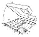
- FIG. 1illustrates an exemplary silicon wafer that may be used to form a silicon interposer for wafer scale assembly of multiple transceiver modules in accordance with the present invention
- FIG. 2illustrates an exemplary arrangement of a combination of a transceiver module-populated silicon interposer wafer with a “lid” wafer, where the lid is ultimately bonded to the interposer wafer to form a packaging of multiple transceiver modules;
- FIG. 3is a cross-sectional view of an exemplary interposer die including plurality of components formed in accordance with the present invention
- FIG. 4is a cross-sectional view of an alternative interposer die structure formed in accordance with the present invention, this structure including an opening to the silicon interposer surface to form an optical reference plane;
- FIG. 5is an isometric view of an exemplary interposer die showing a plurality of openings for supporting the various optical components forming the transceiver arrangement of the present invention
- FIG. 6is a view of the arrangement of FIG. 5 , in this case with the optical and electrical components disposed on the surface of the interposer die;
- FIG. 7is a detailed isometric illustration of an exemplary lens and photodiode component that may be used to capture an incoming optical signal and convert it into an electrical representation;
- FIG. 8is a cut-away side view of the arrangement of FIG. 7 ;
- FIG. 9illustrates the interposer die as shown in FIG. 6 , as well as an exemplary lid component that may be bonded to a fully-populated interposer wafer;
- FIG. 10is an alternative view of the arrangement of FIG. 9 , in this case showing the underside of the lid component;
- FIG. 11illustrates an alternative embodiment of the present invention, in this case where a plurality of four separate laser diodes are disposed on submounts, with the submounts then disposed in openings formed in the interposer;
- FIG. 12shows yet another embodiment of the present invention, in this case where a simplified, single lens array is utilized to provide focusing for both the transmitting and receiving portions of the module;
- FIG. 13is a top view of the arrangement of FIG. 12 ;
- FIG. 14is another embodiment of the present invention where the integrated circuits are stacked to form a “three-dimensional” configuration
- FIG. 15is a top view of a stacked configuration of the present invention.
- FIG. 16is an isometric view of another embodiment of the present invention, in this case utilizing a metal lid to provide additional EMI shielding;
- FIG. 17is a side view of an exemplary embodiment using a metal lid, in this case where the lid is formed to include interior walls to isolate the components form the optical transmitter;
- FIG. 18is a side view of an alternative embodiment of the present invention using a metal lid without any interior walls.
- a significant improvement in fabrication efficiency, without sacrificing the integrity of the necessary precise optical alignments between various individual elements,is provided in accordance with the present invention by utilizing a wafer scale assembly technique, employing a silicon wafer as a carrier substrate (also referred to hereinafter as an interposer) upon which the individual components (including electronic integrated circuits, active optical devices and passive optical devices) are mounted, aligned, bonded, etc.
- a typical silicon waferfor example, an 8′′ wafer
- the wafer-scale fabrication and assembly techniques of the present inventionare capable of improving the efficiencies of transceiver module assembly and packaging processes.
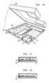
- FIG. Iillustrates an exemplary silicon wafer 10 that may be utilized as an interposer wafer in accordance with the present invention.
- a large number of individual interposer die 12are defined on wafer 10 as being locations where individual transceiver modules are to be assembled.
- a separate lid wafer 14is bonded to interposer wafer 10 in a manner that results in encapsulating each individual transceiver module.
- lid wafer 14is formed to include separate chambers 16 that will form the coverings for the separate transceiver modules (as described in detail below).
- the bonded structureis diced to form the final, individual transceiver modules.
- a laser dicing processis preferred, but it is to be understood that any other suitable process for separating the bonded wafers into separate transceiver modules may also be used.
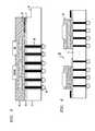
- FIG. 3is a cut-away side view of a portion of an interposer wafer 10 , as processed to be populated with a number of components forming an exemplary transceiver module.
- a buried oxide (BOX) layer 18is formed over top surface 11 of interposer wafer 10 , with a relatively thick interlevel dielectric (ILD) layer 20 formed over BOX layer 18 ,
- ILDinterlevel dielectric
- a relatively thin silicon layer 22is created at the interface between BOX layer 18 and ILD layer 20 , where silicon layer 22 is used as an optical waveguiding layer.
- SOTsilicon-on-insulator
- optical waveguiding layer 22is specifically defined and is routed along this interface to provide the desired optical communication path(s) between the various components forming a transceiver module.
- the planarity of top surface 11 of interposer wafer 10is precisely controlled so that surface 11 functions as an optical reference plane for the transceiver module.
- an optical reference planeallows for passive techniques to be used to provide alignment between various optical components as they process propagating optical signals.
- one or more optical componentscan first be assembled and precisely aligned on a separate submount element, as discussed below in associated with FIG.
- lithographically-defined feature 24which may be used for providing optical I/O connections to interposer wafer 10 .
- interposer wafer 10in the fabrication of transceiver modules is that the necessary connections between the electronic integrated circuit components forming the transceiver module (e.g., laser driver, transimpedance amplifier, etc.) and underlying sources of power, signal, etc., can be created by using conventional vias 26 formed through the thickness of interposer 10 , as shown in FIG. 3 , Either metal or doped silicon material can be used to “fill” vias 26 and form the conductive path between the transceiver module and the power and signal contacts.
- a plurality of solder bumps 28is formed at the termination of vias 26 and used for connection to an associated arrangement of bond pads on a printed circuit board, or other source of power and data signals (not shown).
- FIG. 4is a side view of another embodiment of interposer wafer 10 and included components forming an optical transceiver module.
- This particular embodimentdoes not specifically show BOX layer 18 , but it is to be understood that such a layer may still be included in such a transceiver arrangement.
- Specifically shown in this viewis the processing of ILD layer 20 to form a plurality of openings 30 . As discussed above, these openings 30 are created to expose top surface 11 of silicon interposer wafer 10 , allowing surface 11 to function as a well-defined optical reference plane.
- a selective etchantsuch as HF, for example
- HFa selective etchant
- surface 11 of silicon interposer 10will naturally stop at surface 11 of silicon interposer 10 as predefined regions of ILD layer 20 are removed. Therefore, there is no concern about either over-etching or under-etching and degrading the planarity of surface 11 during the etching process.
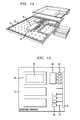
- FIG. 5is an isometric top view of an exemplary interposer die 12 particularly illustrating the creation of a plurality of openings 30 for supporting the various optical components in the predefined, precise locations by virtue of using exposed surface 11 of interposer 10 as a reference plane. While FIG. 5 shows only a single interposer die, it is to be understood that the process of forming these openings, followed by the placement of the various components, is performed as a wafer scale process, where each interposer die 12 of wafer 10 is simultaneously populated with the individual optical and electrical components. In the particular embodiment of FIG. 5 , a plurality of openings 30 are formed to allow for the precise placement of a number of critical optical components.
- openings 30are created to expose top surface 11 of silicon interposer 10 , where surface 11 is precisely defined and controlled to create and maintain a planar optical reference.
- a first opening 30 - 1is used as the location for a laser diode and a second opening 30 - 2 is used to support a lens element.
- openings 30 - 1 and 30 - 2Through the careful control of the location of openings 30 - 1 and 30 - 2 (possible using conventional photolithographic patterning and etching techniques), once the laser diode and lens are inserted in their respective openings, they will be aligned, since each component will be resting on optical reference plane top surface 11 .
- a third opening 30 - 3is used to support an optical isolator, which will then also be in the optical signal path and in alignment with the laser diode and lens. In some cases, active alignment is required to properly align the laser diode with its associated lens.
- a wafer scale active alignment schemeis used, based, for example, on an electro-optic probe comprising a precisely placed detector and/or optical source, turning mirrors and other optics (and, perhaps, electrical probes) to provide alignment and testing of components in a conventional “step and repeat” fashion across the wafer surface.
- wafer scale electrical burn-in of various componentsis accomplished using an electrical probe card in the same step and repeat process.
- an opening 30 - 4is created through ILD layer 20 to support a lens element, with a large opening 30 - 5 positioned behind opening 30 - 4 .
- Large opening 30 - 5is used to support a product-specific CMOS photonic integrated circuit used to perform various types of signal processing (e.g., modulating a CW laser signal with an electrical data signal to create a data-modulated optical output signal). The particular operation of the photonic integrated circuit is not germane to the subject matter of the present invention.
- An opening 30 - 6is used to support a coupling element associated with an output optical signal, with opening 30 - 7 utilized to support an associated optical I/O connection (see, for example, feature 24 as shown in FIG. 3 ).
- a number of vias 26are also shown in FIG. 5 , where in this particular embodiment the vias are disposed in a regular grid pattern across the surface of the complete silicon interposer wafer 10 so that they may be used as needed in different transceiver configurations.
- FIG. 6is a view of the arrangement of FIG. 5 , in this case with the various optical components disposed within their associated openings.
- a laser diode 32is positioned within opening 30 - 1 and a microlens 34 is disposed within opening 30 - 2 .
- An isolator 36is placed within opening 30 - 3 , in the optical output signal path from laser diode 32 .
- the output from isolator 36is then passed through a microlens array 38 disposed within opening 30 - 4 , where the lens array is used to couple the propagating optical signal into a CMOS photonic integrated circuit 40 .
- Various well-known methodsmay be used for affixing the optical components in place in their respective openings.
- epoxy, eutectic bonding or other arrangementsmay be used to permanently attach the optical components in their respective openings. It is to be understood that an appropriate temperature hierarchy needs to first be established such that the stability of the joints are ensured during other potentially high temperature post-processing operations.
- a fiber array connector 42is disposed within opening 30 - 7 , with the individual fibers 44 forming the array used to introduce optical signals to, and output optical signals from, the transceiver module. It is to be noted that opening 30 - 7 may, in some cases, comprise feature 24 that is lithographically formed in manner described above.
- a lens array 46is included within fiber array connector 42 at the termination of the plurality of individual fibers 44 . In operation, incoming optical signals along, for example, optical fibers 44 - 1 and 44 - 2 will pass through lens array 46 , and then impinge a lens element 48 and photodiode 50 disposed within opening 30 - 6 , creating an associated electrical signal representation.
- Lens element 48 and photodiode 50are disposed in opening 30 - 6 , which is formed to be in alignment with opening 30 - 7 (and, more particularly, with the location of fibers 44 - 1 and 44 - 2 within the array).
- Various electrical componentssuch as transimpedance amplifier 33 and a laser driver 35 are also positioned at predetermined locations on interposer die 12 .
- the electrical componentsare disposed on the surface of ILD layer 20 (see FIG. 4 ), with necessary electrical connections made using the vias 26 formed through interposer die 12 .
- lens element 48takes the form of a lens array and includes a plurality of curved surfaces 52 for focusing a plurality of incoming optical signals, as best shown in FIG. 8 .
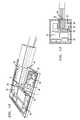
- a prism component 54is used as a 90° turning mirror to redirect the plurality of focused optical signals from a horizontal to a vertical plane, with photodiode 50 (in this case a photodiode array) disposed to receive incoming optical signals. It is to be understood that this is merely one exemplary configuration for receiving incoming optical signals and converting them into an electrical representation. Various other arrangements may be utilized within the wafer-based arrangement of transceiver modules in accordance with the present invention.
- a sealing layer 56is shown as being formed around the perimeter of interposer die 12 (again, it is to be understood that this layer is formed around the perimeter of each die 12 forming interposer wafer 10 ).
- This sealing layerwhich may comprise a glass frit material, a AuSn solder, or any other suitable material, is used to bond a separate lid component to the populated interposer die.
- a lid component 58is formed to match the “footprint” of interposer die 12 and is disposed over die 12 and sealed thereto by the presence of sealing layer 56 . Recalling the discussion associated with FIG. 2 , it is to be understood that a plurality of separate lid components 58 are formed in a separate wafer and, during fabrication, the entire wafer is bonded (via the multiple sealing layers 56 ) to interposer wafer 10 .
- lid component 58is specifically formed to follow the periphery of interposer die 12 as guided by the pattern of sealing layer 56 .
- Bottom surface 60 of lid component 58is coated with a specific material (for example, a metal such as gold) to form a sealing of lid component 58 to interposer die 12 .
- sealing layer 56 and lid component 58are specifically designed to create an opening 62 , which allows for the optical input and output signals to access the transceiver module (for example, opening 62 may be used to allow for optical connector 42 to be inserted, as shown in this particular embodiment).
- FIG. 10is an alternative isometric view of the arrangement of FIG. 9 , showing in particular bottom surface 60 of lid component 58 and illustrating how it follows the same path as sealing layer 56 of interposer die 12 .
- FIG. 11illustrates another embodiment of the present invention where in this case, a set of four separate laser diodes 32 - 1 , 32 - 2 , 32 - 3 and 32 - 4 are included within the transceiver. As shown in FIG. 11 , each laser diode is positioned with an associated lens 34 -i and isolator 36 -i on a submount element 64 .
- submounts 64allows for the optical transmitting subassembly comprising the laser, isolator and lens to be separately mounted and aligned. Thereafter, the set of submounts 64 are disposed in properly-sized openings formed in interposer die 12 (not visible in the view of FIG. 11 ), where the proper placement of the openings for these submounts results in creating the desired optical alignment with an associated fiber array 66 .
- the submountmay comprise a thermo-electric cooler (TEC) component.
- TECthermo-electric cooler
- An exemplary lid component 68is also shown in FIG. 11 , where it is to be understood that lid component 68 is formed to have a depth sufficient to accommodate the raised positioning of the laser diodes.
- FIGS. 12 and 13illustrate yet another embodiment of the present invention, in this case where interposer die 12 is processed to form a single opening 70 for placement of a lens array 72 that is used in conjunction with both transmit and receive optical signals (compare with openings 30 - 4 and 30 - 6 in FIG. 5 , as used to support separate lens elements 38 and 48 , respectively).
- FIG. 12is an isometric view of die 12 , illustrating the location of opening 70 and lens array 72 with respect to both laser diode 32 and fiber connector 42 .
- Input optical signal I from laser diode 32is shown as passing through lens array 72 and entering an integrated transceiver circuit arrangement 74 .
- a set of four output signals Ois shown in this example as exiting integrated transceiver circuit arrangement 74 and passing through lens array 72 so as to be focused into a set of fibers 44 within fiber connector 42 .
- the location of the input and output optical signalsis best seen in the view of FIG. 13 .
- FIG. 14Another embodiment of the present invention is shown in FIG. 14 , which can be thought of as a “three dimensional” transceiver module, where a first integrated circuit is stacked vertically on a second integrated circuit.
- a first integrated circuit 76is defined as an opto-electronic integrated circuit 76 and is responsive to an incoming optical signal to create a modified optical output signal.
- a second integrated circuit 78is defined as an electronic integrated circuit and provides power and electrical data signals to opto-electronic integrated circuit 76 .
- Electronic integrated circuit 78is, itself, electrically coupled to interposer die 12 . As discussed above in association with FIG.
- interposer die 12includes a plurality of silicon through vias 26 which enable the transfer of electrical signals from an associated printed circuit board (not shown) generally disposed underneath interposer 10 and the specific components of the transceiver module. Again, the specific locations of the openings formed through ILD layer 18 is dictated by the various components used to form the transceiver module.
- FIG. 15is a top view of an alternative three-dimensional, stacked transceiver embodiment, where at least some of the associated optical components (in this case, a plurality of optical modulators 80 ) are formed within the silicon waveguiding layer 22 of interposer 10 .
- Monolithic (or hybrid) inclusion of photodiodes 82 within waveguiding layer 22is also possible.
- the ability to integrate various silicon-based components of an optical transceiver directly into the waveguiding layeris another advantage of utilizing a silicon interposer layer—processed at a wafer-scale level—in accordance with the present invention.
- a lithographically-defined feature 86that provides “end fire” coupling of optical signals into waveguiding layer 22 .
- the end terminations of the waveguiding layersare formed as nanotapers to improve coupling efficiency.
- EMIelectro-magnetic interference
- FIG. 16An alternative solution, formed in accordance with the present invention, is shown in FIG. 16 , where a metal lid component 90 is utilized in place of the silicon lids as discussed above.
- sealing layer 56is formed as a metal that will assist in forming a ground connection with metal lid component 90 .
- an additional grounding path 57is formed to encircle the optical transmitting components 32 , 34 and 36 , which are most sensitive to EMI.
- “grounding”is provided by utilizing a special via 92 within interposer die 12 that is positioned to contact a portion of metal lid 90 and provide an electrical connection to a ground plane (not shown) located under interposer die 12 .
- FIG. 16An alternative solution, formed in accordance with the present invention, is shown in FIG. 16 , where a metal lid component 90 is utilized in place of the silicon lids as discussed above.
- sealing layer 56is formed as a metal that will assist in forming a ground connection with metal lid component 90 .
- an additional grounding path 57is formed to
- FIG. 17is a simplified side view of this arrangement showing the interconnection of metal lid 90 and a ground plane 94 through via 92 of interposer die 12 .
- a side view of an alternative embodiment using a metal lid 90is shown in FIG. 18 , where this embodiment does not include a separate shielding configuration around the optical transmitting components.
Landscapes
- Physics & Mathematics (AREA)
- General Physics & Mathematics (AREA)
- Optics & Photonics (AREA)
- Engineering & Computer Science (AREA)
- Microelectronics & Electronic Packaging (AREA)
- Computer Hardware Design (AREA)
- Condensed Matter Physics & Semiconductors (AREA)
- Power Engineering (AREA)
- Manufacturing & Machinery (AREA)
- Semiconductor Lasers (AREA)
- Light Receiving Elements (AREA)
- Optical Couplings Of Light Guides (AREA)
- Testing Of Individual Semiconductor Devices (AREA)
Abstract
Description
- This application claims the benefit of the following U.S. Provisional Applications: Ser. No. 61/482,705, filed May 5, 2011; Ser. No. 61/509,290, filed Jul. 19, 2011; Ser. No. 61/526,821, filed Aug. 24, 2011; Ser. No. 61/543,240, filed Oct. 4, 2011; and Ser. No. 61/560,378, filed Nov. 16, 2011, all of which are incorporated by reference herein.
- The present invention relates to a wafer scale implementation of opto-electronic transceivers and, more particularly, to the utilization of a silicon wafer as an optical reference plane and platform upon which all necessary optical and electronic components are assembled for a multiple number of transceivers in a wafer scale process.
- In optical communication networks, transceivers are used to transmit and receive optical signals over optical fibers or other types of optical waveguides. On the transmit side of the transceiver, a laser diode and associated circuitry is used to generate a modulated optical signal (representing data) that is ultimately coupled into an output signal path (fiber, waveguide, etc.). On the receive side of the transceiver, one or more incoming optical signals are converted from optical signals into electrical signals within a photodiode or similar device. Inasmuch as the electrical signal is very weak, an amplifying device (for example, a transimpedance amplifier) is typically used to boost the signal strength before attempting to recover the data information from the received signal.
- Optical transceiver modules thus comprise a number of separate components that require precise placement relative to one another. As the components are being assembled, active optical alignment is required to ensure that the integrity of the optical signal path is maintained. In most cases, these transceiver modules are built as individual units and, as a result, the need to perform active optical alignment on a unit-by-unit basis becomes expensive and time-consuming.
- As the demand for optical transceiver modules continues to increase, the individual unit assembly approach becomes problematic and, therefore, a need remains for a different approach to optical transceiver assembly that can improve the efficiency of the construction process while preserving the integrity of module, including the required precise optical alignment between elements.
- The need remaining in the art is addressed by the present invention, which relates to a wafer scale implementation of an opto-electronic transceiver assembly process and, more particularly, to the utilization of a silicon wafer as an optical reference plane and platform upon which all necessary optical and electronic components are simultaneously assembled for a plurality of separate transceiver modules.
- In accordance with the present invention, a silicon wafer is utilized as a “platform” (also referred to hereinafter as an interposer) upon which all of the components for a multiple number of transceiver modules are mounted or integrated, with the top surface of the silicon interposer used as a reference plane for defining the optical signal path between separate optical components. Indeed, a single silicon wafer is used as the platform for a large number of separate transceiver modules, providing the ability to use a wafer scale assembly process, as well as optical alignment and testing of these modules, addressing the concerns of the prior art as mentioned above.
- In further accordance with the present invention, the utilization of a silicon interposer allows for various through-silicon vias to be formed and used to provide electrical connections between components placed on the interposer and underlying electrical components. Electronic integrated circuits such as laser drivers, micro-controllers and transimpedance amplifiers are accurately placed on the silicon interposer using photolithographically-aided features formed on the interposer. Wafer scale wirebonding techniques are used to create the necessary electrical connections between the individual elements. Optical components such as lasers, isolators, lenses (individual and arrays), photodiodes and the like are placed within lithographically-defined openings on the interposer, where the ability accurately and precisely define the location and size of openings using conventional CMOS fabrication techniques allows for passive optical alignment processes to be used where appropriate.
- It is an aspect of the present invention that the wafer scale assembly of multiple transceiver modules allows for a wafer scale active alignment scheme to be used when necessary, based on an electro-optic probe containing a precisely placed detector and/or optical source, turning mirrors and other optics, as well as electrical probes. By virtue of the wafer scale assembly of the transceiver modules, the placement of components and subsequent alignment and testing can be performed in a conventional “step and repeat” fashion.
- In one embodiment of the present invention, a second wafer is used as a “lid” for the assembled modules, with the lid wafer first being etched and processed to define separate cavities within which the individual transceiver modules will be located. The lid may be formed of glass, silicon or any other suitable material. A wafer-to-wafer bonding of the arrangement results in creating the final wafer scale transceiver assembly, which can then be diced to create the separate, individual transceiver modules.
- In an alternative embodiment, a metal lid may be used in situations (high bandwidth, high frequency, for example) that have more stringent requirements with respect to EMI shielding.
- A particular embodiment of the present invention comprises a wafer scale arrangement of optical transceiver modules including a silicon interposer wafer for use as a platform for assembling a plurality of separate transceiver modules, the silicon interposer wafer defined as comprising a planar top surface defining an optical reference plane, a plurality of conductive vias formed therethrough to provide electrical connections to other components and optical waveguiding regions formed along the surface thereof and a dielectric layer formed over the planar top surface of the silicon interposer wafer, the dielectric layer for supporting the placement and interconnection of electrical integrated circuit components associated with a plurality of separate transceiver modules, the dielectric layer configured to include a plurality of openings formed therethrough so as to expose the planar top surface of the silicon interposer wafer in each opening, the plurality of openings of predetermined size and disposed in predetermined locations for properly positioning and aligning optical components of each transceiver module, the dielectric layer further including electrical conductive paths for providing electrical connection between the supported electrical integrated circuit components and selected ones of the conductive vias of the underlying silicon wafer.
- Other and further aspects and advantages of the present invention will become apparent during the course of the following discussion and by reference to the accompanying drawings.
- Referring now to the drawings, where like numerals represent like elements in several views:
FIG. 1 illustrates an exemplary silicon wafer that may be used to form a silicon interposer for wafer scale assembly of multiple transceiver modules in accordance with the present invention;FIG. 2 illustrates an exemplary arrangement of a combination of a transceiver module-populated silicon interposer wafer with a “lid” wafer, where the lid is ultimately bonded to the interposer wafer to form a packaging of multiple transceiver modules;FIG. 3 is a cross-sectional view of an exemplary interposer die including plurality of components formed in accordance with the present invention;FIG. 4 is a cross-sectional view of an alternative interposer die structure formed in accordance with the present invention, this structure including an opening to the silicon interposer surface to form an optical reference plane;FIG. 5 is an isometric view of an exemplary interposer die showing a plurality of openings for supporting the various optical components forming the transceiver arrangement of the present invention;FIG. 6 is a view of the arrangement ofFIG. 5 , in this case with the optical and electrical components disposed on the surface of the interposer die;FIG. 7 is a detailed isometric illustration of an exemplary lens and photodiode component that may be used to capture an incoming optical signal and convert it into an electrical representation;FIG. 8 is a cut-away side view of the arrangement ofFIG. 7 ;FIG. 9 illustrates the interposer die as shown inFIG. 6 , as well as an exemplary lid component that may be bonded to a fully-populated interposer wafer;FIG. 10 is an alternative view of the arrangement ofFIG. 9 , in this case showing the underside of the lid component;FIG. 11 illustrates an alternative embodiment of the present invention, in this case where a plurality of four separate laser diodes are disposed on submounts, with the submounts then disposed in openings formed in the interposer;FIG. 12 shows yet another embodiment of the present invention, in this case where a simplified, single lens array is utilized to provide focusing for both the transmitting and receiving portions of the module;FIG. 13 is a top view of the arrangement ofFIG. 12 ;FIG. 14 is another embodiment of the present invention where the integrated circuits are stacked to form a “three-dimensional” configuration;FIG. 15 is a top view of a stacked configuration of the present invention;FIG. 16 is an isometric view of another embodiment of the present invention, in this case utilizing a metal lid to provide additional EMI shielding;FIG. 17 is a side view of an exemplary embodiment using a metal lid, in this case where the lid is formed to include interior walls to isolate the components form the optical transmitter; andFIG. 18 is a side view of an alternative embodiment of the present invention using a metal lid without any interior walls.- In the following description, for purposes of explanation and not limitation, specific details are set forth in order to provide a thorough understanding of the present invention. However, it will be apparent to one skilled in the art that the present invention may be practiced in other embodiments that depart from these specific details. In other instances, detailed descriptions of well-known devices and methods are omitted so as not to obscure the description of the present invention with unnecessary details.
- As mentioned above, a significant improvement in fabrication efficiency, without sacrificing the integrity of the necessary precise optical alignments between various individual elements, is provided in accordance with the present invention by utilizing a wafer scale assembly technique, employing a silicon wafer as a carrier substrate (also referred to hereinafter as an interposer) upon which the individual components (including electronic integrated circuits, active optical devices and passive optical devices) are mounted, aligned, bonded, etc. Since a typical silicon wafer (for example, an 8″ wafer) can support the creation of multiple transceiver modules (e.g., tens of die across the wafer surface), the wafer-scale fabrication and assembly techniques of the present invention are capable of improving the efficiencies of transceiver module assembly and packaging processes.
- Prior to describing the details associated with using a silicon wafer as an interposer or platform, the following discussion, with reference to
FIGS. 1 and 2 , will provide an overall understanding of the benefits of using a wafer scale process to assemble the transceivers in the first instance. - FIG. I illustrates an
exemplary silicon wafer 10 that may be utilized as an interposer wafer in accordance with the present invention. As shown, a large number ofindividual interposer die 12 are defined onwafer 10 as being locations where individual transceiver modules are to be assembled. Oncewafer 10 is fully populated with the multiple transceiver modules, aseparate lid wafer 14, as shown inFIG. 2 , is bonded to interposerwafer 10 in a manner that results in encapsulating each individual transceiver module. In particular,lid wafer 14 is formed to includeseparate chambers 16 that will form the coverings for the separate transceiver modules (as described in detail below). Once the wafers are joined, the bonded structure is diced to form the final, individual transceiver modules. A laser dicing process is preferred, but it is to be understood that any other suitable process for separating the bonded wafers into separate transceiver modules may also be used. - With this understanding of the overall wafer-based approach to creating transceiver modules, the following discussion will focus on the aspects associated with utilizing a silicon interposer platform in the assembly of exemplary transceiver embodiments. It is to be understood that in drawings where only a single transceiver arrangement shown, the actual assembly process creates multiple transceiver modules across the surface of the interposer wafer, at each separate die location (or at least at a subset of the die locations, as need be, based upon need, wafer quality and the like), as shown in
FIG. 1 . FIG. 3 is a cut-away side view of a portion of aninterposer wafer 10, as processed to be populated with a number of components forming an exemplary transceiver module. In this case, a buried oxide (BOX)layer 18 is formed overtop surface 11 ofinterposer wafer 10, with a relatively thick interlevel dielectric (ILD)layer 20 formed overBOX layer 18, A relativelythin silicon layer 22 is created at the interface betweenBOX layer 18 andILD layer 20, wheresilicon layer 22 is used as an optical waveguiding layer. Indeed, it is seen that the combination ofinterposer wafer 10,BOX layer 18 andsilicon layer 22 forms a well-known silicon-on-insulator (SOT) optical structure that has been extensively used in recent years in the creation of passive and active optical components.- As will be discussed hereinbelow,
optical waveguiding layer 22 is specifically defined and is routed along this interface to provide the desired optical communication path(s) between the various components forming a transceiver module. In accordance with the present invention, the planarity oftop surface 11 ofinterposer wafer 10 is precisely controlled so thatsurface 11 functions as an optical reference plane for the transceiver module. As a result, and discussed in detail below, the creation of an optical reference plane allows for passive techniques to be used to provide alignment between various optical components as they process propagating optical signals. In an alternative embodiment, one or more optical components can first be assembled and precisely aligned on a separate submount element, as discussed below in associated withFIG. 11 , with the submount then precisely placed onsurface 11 ofinterposer 10, avoiding the need to perform multiple wafer scale active alignments. Also shown in the view ofFIG. 3 is a lithographically-definedfeature 24, which may be used for providing optical I/O connections tointerposer wafer 10. - Another advantage of utilizing
interposer wafer 10 in the fabrication of transceiver modules is that the necessary connections between the electronic integrated circuit components forming the transceiver module (e.g., laser driver, transimpedance amplifier, etc.) and underlying sources of power, signal, etc., can be created by usingconventional vias 26 formed through the thickness ofinterposer 10, as shown inFIG. 3 , Either metal or doped silicon material can be used to “fill”vias 26 and form the conductive path between the transceiver module and the power and signal contacts. In the specific embodiment shown inFIG. 3 , a plurality of solder bumps28 is formed at the termination ofvias 26 and used for connection to an associated arrangement of bond pads on a printed circuit board, or other source of power and data signals (not shown). FIG. 4 is a side view of another embodiment ofinterposer wafer 10 and included components forming an optical transceiver module. This particular embodiment does not specifically showBOX layer 18, but it is to be understood that such a layer may still be included in such a transceiver arrangement. Specifically shown in this view is the processing ofILD layer 20 to form a plurality ofopenings 30. As discussed above, theseopenings 30 are created to exposetop surface 11 ofsilicon interposer wafer 10, allowingsurface 11 to function as a well-defined optical reference plane. Advantageously, it is possible to use standard photolithographic patterning and etching techniques to formopenings 30 with precise geometries and in precise locations relative to other components forming the transceiver so as to provide for passive optical alignments, where possible, between various components. Indeed, a selective etchant (such as HF, for example) will naturally stop atsurface 11 ofsilicon interposer 10 as predefined regions ofILD layer 20 are removed. Therefore, there is no concern about either over-etching or under-etching and degrading the planarity ofsurface 11 during the etching process.FIG. 5 is an isometric top view of an exemplary interposer die12 particularly illustrating the creation of a plurality ofopenings 30 for supporting the various optical components in the predefined, precise locations by virtue of using exposedsurface 11 ofinterposer 10 as a reference plane. WhileFIG. 5 shows only a single interposer die, it is to be understood that the process of forming these openings, followed by the placement of the various components, is performed as a wafer scale process, where each interposer die12 ofwafer 10 is simultaneously populated with the individual optical and electrical components. In the particular embodiment ofFIG. 5 , a plurality ofopenings 30 are formed to allow for the precise placement of a number of critical optical components. As described above,openings 30 are created to exposetop surface 11 ofsilicon interposer 10, wheresurface 11 is precisely defined and controlled to create and maintain a planar optical reference. For example, a first opening30-1 is used as the location for a laser diode and a second opening30-2 is used to support a lens element.- Through the careful control of the location of openings30-1 and30-2 (possible using conventional photolithographic patterning and etching techniques), once the laser diode and lens are inserted in their respective openings, they will be aligned, since each component will be resting on optical reference
plane top surface 11. Similarly, a third opening30-3 is used to support an optical isolator, which will then also be in the optical signal path and in alignment with the laser diode and lens. In some cases, active alignment is required to properly align the laser diode with its associated lens. In that event, a wafer scale active alignment scheme is used, based, for example, on an electro-optic probe comprising a precisely placed detector and/or optical source, turning mirrors and other optics (and, perhaps, electrical probes) to provide alignment and testing of components in a conventional “step and repeat” fashion across the wafer surface. Similarly, wafer scale electrical burn-in of various components (such as, for example, a laser diode) is accomplished using an electrical probe card in the same step and repeat process. - Continuing with the description of
FIG. 5 , an opening30-4 is created throughILD layer 20 to support a lens element, with a large opening30-5 positioned behind opening30-4. Large opening30-5 is used to support a product-specific CMOS photonic integrated circuit used to perform various types of signal processing (e.g., modulating a CW laser signal with an electrical data signal to create a data-modulated optical output signal). The particular operation of the photonic integrated circuit is not germane to the subject matter of the present invention. An opening30-6 is used to support a coupling element associated with an output optical signal, with opening30-7 utilized to support an associated optical I/O connection (see, for example, feature24 as shown inFIG. 3 ). A number ofvias 26 are also shown inFIG. 5 , where in this particular embodiment the vias are disposed in a regular grid pattern across the surface of the completesilicon interposer wafer 10 so that they may be used as needed in different transceiver configurations. FIG. 6 is a view of the arrangement ofFIG. 5 , in this case with the various optical components disposed within their associated openings. As shown, alaser diode 32 is positioned within opening30-1 and amicrolens 34 is disposed within opening30-2. Anisolator 36 is placed within opening30-3, in the optical output signal path fromlaser diode 32. The output fromisolator 36 is then passed through amicrolens array 38 disposed within opening30-4, where the lens array is used to couple the propagating optical signal into a CMOS photonic integratedcircuit 40. Various well-known methods may be used for affixing the optical components in place in their respective openings. In particular, epoxy, eutectic bonding or other arrangements may be used to permanently attach the optical components in their respective openings. It is to be understood that an appropriate temperature hierarchy needs to first be established such that the stability of the joints are ensured during other potentially high temperature post-processing operations.- In the specific embodiment shown in
FIG. 6 , afiber array connector 42 is disposed within opening30-7, with theindividual fibers 44 forming the array used to introduce optical signals to, and output optical signals from, the transceiver module. It is to be noted that opening30-7 may, in some cases, comprisefeature 24 that is lithographically formed in manner described above. In this embodiment, alens array 46 is included withinfiber array connector 42 at the termination of the plurality ofindividual fibers 44. In operation, incoming optical signals along, for example, optical fibers44-1 and44-2 will pass throughlens array 46, and then impinge alens element 48 andphotodiode 50 disposed within opening30-6, creating an associated electrical signal representation.Lens element 48 andphotodiode 50, as shown inFIG. 6 , are disposed in opening30-6, which is formed to be in alignment with opening30-7 (and, more particularly, with the location of fibers44-1 and44-2 within the array). Various electrical components, such astransimpedance amplifier 33 and alaser driver 35 are also positioned at predetermined locations on interposer die12. Here, the electrical components are disposed on the surface of ILD layer20 (seeFIG. 4 ), with necessary electrical connections made using thevias 26 formed through interposer die12. - An exemplary combination of
lens element 48 andphotodiode 50 is shown inFIGS. 7 and 8 , whereFIG. 7 is an isometric view, andFIG. 8 is a cut-away side view. In this particular embodiment,lens element 48 takes the form of a lens array and includes a plurality ofcurved surfaces 52 for focusing a plurality of incoming optical signals, as best shown inFIG. 8 . Aprism component 54 is used as a 90° turning mirror to redirect the plurality of focused optical signals from a horizontal to a vertical plane, with photodiode50 (in this case a photodiode array) disposed to receive incoming optical signals. It is to be understood that this is merely one exemplary configuration for receiving incoming optical signals and converting them into an electrical representation. Various other arrangements may be utilized within the wafer-based arrangement of transceiver modules in accordance with the present invention. - Referring back to
FIG. 6 , asealing layer 56 is shown as being formed around the perimeter of interposer die12 (again, it is to be understood that this layer is formed around the perimeter of each die12 forming interposer wafer10). This sealing layer, which may comprise a glass frit material, a AuSn solder, or any other suitable material, is used to bond a separate lid component to the populated interposer die. In accordance with the present invention, and shown below inFIG. 9 , alid component 58 is formed to match the “footprint” of interposer die12 and is disposed over die12 and sealed thereto by the presence of sealinglayer 56. Recalling the discussion associated withFIG. 2 , it is to be understood that a plurality ofseparate lid components 58 are formed in a separate wafer and, during fabrication, the entire wafer is bonded (via the multiple sealing layers56) tointerposer wafer 10. - Turning to
FIG. 9 , it is evident thatlid component 58 is specifically formed to follow the periphery of interposer die12 as guided by the pattern of sealinglayer 56.Bottom surface 60 oflid component 58 is coated with a specific material (for example, a metal such as gold) to form a sealing oflid component 58 to interposer die12. As shown inFIG. 9 , sealinglayer 56 andlid component 58 are specifically designed to create anopening 62, which allows for the optical input and output signals to access the transceiver module (for example, opening62 may be used to allow foroptical connector 42 to be inserted, as shown in this particular embodiment).FIG. 10 is an alternative isometric view of the arrangement ofFIG. 9 , showing in particularbottom surface 60 oflid component 58 and illustrating how it follows the same path as sealinglayer 56 of interposer die12. - As mentioned above, an advantageous feature of utilizing a silicon wafer interposer for assembling, aligning and testing transceiver modules on a wafer-scale basis is that the silicon interposer may easily be fabricated to accommodate various arrangements of the different components forming the transceiver. Indeed, some arrangements may use multiple laser inputs, external laser inputs, or other various embodiments.
FIG. 11 illustrates another embodiment of the present invention where in this case, a set of four separate laser diodes32-1,32-2,32-3 and32-4 are included within the transceiver. As shown inFIG. 11 , each laser diode is positioned with an associated lens34-i and isolator36-i on asubmount element 64. The use ofsubmounts 64 allows for the optical transmitting subassembly comprising the laser, isolator and lens to be separately mounted and aligned. Thereafter, the set ofsubmounts 64 are disposed in properly-sized openings formed in interposer die12 (not visible in the view ofFIG. 11 ), where the proper placement of the openings for these submounts results in creating the desired optical alignment with an associatedfiber array 66. In an exemplary embodiment, the submount may comprise a thermo-electric cooler (TEC) component. Anexemplary lid component 68 is also shown inFIG. 11 , where it is to be understood thatlid component 68 is formed to have a depth sufficient to accommodate the raised positioning of the laser diodes. FIGS. 12 and 13 illustrate yet another embodiment of the present invention, in this case where interposer die12 is processed to form asingle opening 70 for placement of alens array 72 that is used in conjunction with both transmit and receive optical signals (compare with openings30-4 and30-6 inFIG. 5 , as used to supportseparate lens elements ILD layer 20 to provide the desired openings (of the proper dimensions) in the locations associated with a particular transceiver module arrangement, while always maintaining the optical reference plane defined bytop surface 11 ofinterposer wafer 10.FIG. 12 is an isometric view ofdie 12, illustrating the location of opening70 andlens array 72 with respect to bothlaser diode 32 andfiber connector 42. Input optical signal I fromlaser diode 32 is shown as passing throughlens array 72 and entering an integrated transceiver circuit arrangement74. A set of four output signals O is shown in this example as exiting integrated transceiver circuit arrangement74 and passing throughlens array 72 so as to be focused into a set offibers 44 withinfiber connector 42. The location of the input and output optical signals is best seen in the view ofFIG. 13 .- Another embodiment of the present invention is shown in
FIG. 14 , which can be thought of as a “three dimensional” transceiver module, where a first integrated circuit is stacked vertically on a second integrated circuit. As shown, a firstintegrated circuit 76 is defined as an opto-electronicintegrated circuit 76 and is responsive to an incoming optical signal to create a modified optical output signal. A secondintegrated circuit 78 is defined as an electronic integrated circuit and provides power and electrical data signals to opto-electronicintegrated circuit 76. Electronicintegrated circuit 78 is, itself, electrically coupled to interposer die12. As discussed above in association withFIG. 3 , interposer die12 includes a plurality of silicon throughvias 26 which enable the transfer of electrical signals from an associated printed circuit board (not shown) generally disposed underneathinterposer 10 and the specific components of the transceiver module. Again, the specific locations of the openings formed throughILD layer 18 is dictated by the various components used to form the transceiver module. - It is a particular advantage of using a silicon interposer with the stacked arrangement of
FIG. 14 that a multi-level metallization within ILD layer20 (as shown inFIG. 3 ) can be used to provide a large number of interconnections to different circuits within a minimal space on the interposer die itself (i.e., a “high density” arrangement).FIG. 15 is a top view of an alternative three-dimensional, stacked transceiver embodiment, where at least some of the associated optical components (in this case, a plurality of optical modulators80) are formed within thesilicon waveguiding layer 22 ofinterposer 10. Monolithic (or hybrid) inclusion ofphotodiodes 82 withinwaveguiding layer 22 is also possible. Indeed, the ability to integrate various silicon-based components of an optical transceiver directly into the waveguiding layer is another advantage of utilizing a silicon interposer layer—processed at a wafer-scale level—in accordance with the present invention. Also shown in this view is a lithographically-defined feature86 that provides “end fire” coupling of optical signals intowaveguiding layer 22. In a preferred embodiment, the end terminations of the waveguiding layers are formed as nanotapers to improve coupling efficiency. - In some applications of systems utilizing transceivers formed in the manner described above, the performance of high speed, high frequency signals is adversely impacted by the presence of electro-magnetic interference (EMI). In the above-described arrangements, an additional ground pad (or ring) was required to be formed on interposer die12 and then connected to a ground plane.
- An alternative solution, formed in accordance with the present invention, is shown in
FIG. 16 , where ametal lid component 90 is utilized in place of the silicon lids as discussed above. Referring toFIG. 16 , sealinglayer 56 is formed as a metal that will assist in forming a ground connection withmetal lid component 90. In this particular embodiment, anadditional grounding path 57 is formed to encircle theoptical transmitting components metal lid 90 and provide an electrical connection to a ground plane (not shown) located under interposer die12.FIG. 17 is a simplified side view of this arrangement showing the interconnection ofmetal lid 90 and aground plane 94 through via92 of interposer die12. A side view of an alternative embodiment using ametal lid 90 is shown inFIG. 18 , where this embodiment does not include a separate shielding configuration around the optical transmitting components. - It is to be understood that the embodiments of the present invention as described above are intended to be exemplary only. The scope of the present invention is therefore intended to be limited only by the scope of the claims appended hereto.
Claims (18)
Priority Applications (5)
| Application Number | Priority Date | Filing Date | Title |
|---|---|---|---|
| US13/463,408US8803269B2 (en) | 2011-05-05 | 2012-05-03 | Wafer scale packaging platform for transceivers |
| CN201280033527.3ACN103650140B (en) | 2011-05-05 | 2012-05-04 | Wafer-class encapsulation platform for transceiver |
| EP12779763.7AEP2705534A4 (en) | 2011-05-05 | 2012-05-04 | PLATFORM ENCAPSULATION PLATFORM FOR TRANSCEIVERS |
| PCT/US2012/036582WO2012151520A2 (en) | 2011-05-05 | 2012-05-04 | Wafer scale packaging platform for transceivers |
| US14/276,566US9343450B2 (en) | 2011-05-05 | 2014-05-13 | Wafer scale packaging platform for transceivers |
Applications Claiming Priority (6)
| Application Number | Priority Date | Filing Date | Title |
|---|---|---|---|
| US201161482705P | 2011-05-05 | 2011-05-05 | |
| US201161509290P | 2011-07-19 | 2011-07-19 | |
| US201161526821P | 2011-08-24 | 2011-08-24 | |
| US201161543240P | 2011-10-04 | 2011-10-04 | |
| US201161560378P | 2011-11-16 | 2011-11-16 | |
| US13/463,408US8803269B2 (en) | 2011-05-05 | 2012-05-03 | Wafer scale packaging platform for transceivers |
Related Child Applications (1)
| Application Number | Title | Priority Date | Filing Date |
|---|---|---|---|
| US14/276,566DivisionUS9343450B2 (en) | 2011-05-05 | 2014-05-13 | Wafer scale packaging platform for transceivers |
Publications (2)
| Publication Number | Publication Date |
|---|---|
| US20120280344A1true US20120280344A1 (en) | 2012-11-08 |
| US8803269B2 US8803269B2 (en) | 2014-08-12 |
Family
ID=47089696
Family Applications (2)
| Application Number | Title | Priority Date | Filing Date |
|---|---|---|---|
| US13/463,408Expired - Fee RelatedUS8803269B2 (en) | 2011-05-05 | 2012-05-03 | Wafer scale packaging platform for transceivers |
| US14/276,566Active2032-06-28US9343450B2 (en) | 2011-05-05 | 2014-05-13 | Wafer scale packaging platform for transceivers |
Family Applications After (1)
| Application Number | Title | Priority Date | Filing Date |
|---|---|---|---|
| US14/276,566Active2032-06-28US9343450B2 (en) | 2011-05-05 | 2014-05-13 | Wafer scale packaging platform for transceivers |
Country Status (4)
| Country | Link |
|---|---|
| US (2) | US8803269B2 (en) |
| EP (1) | EP2705534A4 (en) |
| CN (1) | CN103650140B (en) |
| WO (1) | WO2012151520A2 (en) |
Cited By (28)
| Publication number | Priority date | Publication date | Assignee | Title |
|---|---|---|---|---|
| US8518748B1 (en)* | 2011-06-29 | 2013-08-27 | Western Digital (Fremont), Llc | Method and system for providing a laser submount for an energy assisted magnetic recording head |
| US20140270627A1 (en)* | 2013-03-15 | 2014-09-18 | Compass Electro-Optical Systems Ltd. | Eo device for processing data signals |
| US20140321815A1 (en)* | 2013-04-26 | 2014-10-30 | Hon Hai Precision Industry Co., Ltd. | Optical connector and circuit board of same |
| US20150125110A1 (en)* | 2013-11-04 | 2015-05-07 | Cisco Technology, Inc. | Passively Placed Vertical Optical Connector |
| WO2016050243A1 (en)* | 2014-09-30 | 2016-04-07 | Technische Universität Berlin | Optoelectronic component |
| US9343450B2 (en) | 2011-05-05 | 2016-05-17 | Cisco Technology, Inc. | Wafer scale packaging platform for transceivers |
| US20170148955A1 (en)* | 2015-11-22 | 2017-05-25 | Cyntec Co., Ltd. | Method of wafer level packaging of a module |
| US20170186738A1 (en)* | 2015-03-13 | 2017-06-29 | Kabushiki Kaisha Toshiba | Semiconductor module |
| US9835809B2 (en) | 2016-03-28 | 2017-12-05 | Cisco Technology, Inc. | Alignment of optical components using nanomagnets |
| US20180113256A1 (en)* | 2016-10-20 | 2018-04-26 | Stmicroelectronics S.R.L. | Optical coupling system, corresponding device and method |
| US20180143374A1 (en)* | 2016-11-23 | 2018-05-24 | The Research Foundation For The State University Of New York | Photonics interposer optoelectronics |
| WO2018098146A1 (en)* | 2016-11-23 | 2018-05-31 | The Research Foundation For The State University Of New York | Photonics interposer optoelectronics |
| US20180241174A1 (en)* | 2014-04-16 | 2018-08-23 | Apple Inc. | Active silicon optical bench |
| US20190088697A1 (en)* | 2016-05-25 | 2019-03-21 | Towerjazz Panasonic Semiconductor Co., Ltd. | Solid-state imaging element |
| US10241264B2 (en) | 2016-07-01 | 2019-03-26 | Advanced Semiconductor Engineering, Inc. | Semiconductor device packages |
| US20190324203A1 (en)* | 2018-04-24 | 2019-10-24 | Apple Inc. | Photonic integrated circuit with laser and isolator |
| US10985524B1 (en) | 2018-08-29 | 2021-04-20 | Apple Inc. | High-power hybrid silicon-photonics laser |
| US11256046B2 (en)* | 2014-10-27 | 2022-02-22 | Nokia Solutions And Networks Oy | Photonic interface for electronic circuit |
| US11372181B2 (en)* | 2020-06-12 | 2022-06-28 | Fujitsu Optical Components Limited | Optical module |
| US11443998B2 (en)* | 2019-06-05 | 2022-09-13 | Te Connectivity Solutions Gmbh | Electronic assembly including optical modules |
| US20220397727A1 (en)* | 2021-06-09 | 2022-12-15 | Cisco Technology, Inc. | Connecting optical connector with co-packaged optical device |
| US11585991B2 (en) | 2019-02-28 | 2023-02-21 | Teramount Ltd. | Fiberless co-packaged optics |
| US11782225B2 (en) | 2019-11-19 | 2023-10-10 | Corning Research & Development Corporation | Multi-fiber interface apparatus for photonic integrated circuit |
| US11852876B2 (en) | 2015-10-08 | 2023-12-26 | Teramount Ltd. | Optical coupling |
| US12124087B2 (en) | 2015-10-08 | 2024-10-22 | Teramount Ltd. | Wideband surface coupling |
| US12164159B2 (en) | 2021-12-22 | 2024-12-10 | Teramount Ltd. | Backside optical connector |
| US12265259B2 (en) | 2019-01-23 | 2025-04-01 | Teramount Ltd. | Waveguide mode coupling |
| US12379555B2 (en) | 2021-10-27 | 2025-08-05 | Teramount Ltd. | Detachable connector for co-packaged optics |
Families Citing this family (14)
| Publication number | Priority date | Publication date | Assignee | Title |
|---|---|---|---|---|
| EP2769253B1 (en)* | 2011-10-19 | 2020-07-15 | Cisco Technology, Inc. | Molded glass lid for wafer level packaging of opto-electronic assemblies |
| US9419718B2 (en)* | 2014-08-18 | 2016-08-16 | Cisco Technology, Inc. | Aligning optical components in a multichannel receiver or transmitter platform |
| US10209464B2 (en)* | 2014-10-17 | 2019-02-19 | Cisco Technology, Inc. | Direct printed circuit routing to stacked opto-electrical IC packages |
| US9910232B2 (en)* | 2015-10-21 | 2018-03-06 | Luxtera, Inc. | Method and system for a chip-on-wafer-on-substrate assembly |
| US9575267B1 (en) | 2015-11-03 | 2017-02-21 | Cisco Technology, Inc. | Passive alignment of optical components using optical fiber stubs |
| US9389362B1 (en) | 2015-11-16 | 2016-07-12 | International Business Machines Corporation | Adaptive optical interconnection of components of an electro-optical circuit |
| US9971096B2 (en)* | 2016-06-01 | 2018-05-15 | Cisco Technology, Inc. | Passive fiber optic butt coupling using a semiconductor etched feature |
| CN106252389B (en)* | 2016-09-05 | 2023-03-21 | 飞昂创新科技南通有限公司 | Anti-interference semiconductor device for optical transceiver |
| CN211826618U (en)* | 2017-03-07 | 2020-10-30 | 康宁光电通信有限责任公司 | Optical subassembly for converting data between optical and electrical formats |
| US10866367B2 (en) | 2018-07-10 | 2020-12-15 | Corning Research & Development Corporation | Wafer-level lenses for fiber optic connectors and methods for making the same |
| KR102506645B1 (en)* | 2019-10-28 | 2023-03-07 | 한국전자통신연구원 | Cooling optical transmission module device and manufacturing method thereof |
| US20220413237A1 (en)* | 2021-06-25 | 2022-12-29 | Henning Braunisch | Apparatus and method of manufacturing a vertically disaggregated photonic device |
| US11835777B2 (en)* | 2022-03-18 | 2023-12-05 | Celestial Ai Inc. | Optical multi-die interconnect bridge (OMIB) |
| TWI890150B (en)* | 2023-09-26 | 2025-07-11 | 財團法人工業技術研究院 | Semiconductor package and manufacturing method thereof |
Citations (37)
| Publication number | Priority date | Publication date | Assignee | Title |
|---|---|---|---|---|
| US4811082A (en)* | 1986-11-12 | 1989-03-07 | International Business Machines Corporation | High performance integrated circuit packaging structure |
| US5949246A (en)* | 1997-01-28 | 1999-09-07 | International Business Machines | Test head for applying signals in a burn-in test of an integrated circuit |
| US20020180027A1 (en)* | 2001-05-31 | 2002-12-05 | Yoshihide Yamaguchi | Semiconductor module and method of making the device |
| US6794273B2 (en)* | 2002-05-24 | 2004-09-21 | Fujitsu Limited | Semiconductor device and manufacturing method thereof |
| US20050136634A1 (en)* | 2003-12-17 | 2005-06-23 | Sergey Savastiouk | Integrated circuits and packaging substrates with cavities, and attachment methods including insertion of protruding contact pads into cavities |
| US20060044433A1 (en)* | 2004-08-31 | 2006-03-02 | Micron Technology, Inc. | Microelectronic imagers having front side contacts and methods of packaging such microelectronic imagers |
| US20070080458A1 (en)* | 2005-10-11 | 2007-04-12 | Tsuyoshi Ogawa | Hybrid module and method of manufacturing the same |
| US7265330B2 (en)* | 2004-07-19 | 2007-09-04 | Micron Technology, Inc. | Microelectronic imagers with optical devices and methods of manufacturing such microelectronic imagers |
| US7266262B2 (en)* | 2002-10-24 | 2007-09-04 | Sony Corporation | Hybrid circuit substrate with optical and electrical interconnects, hybrid circuit module with optical and electrical interconnects and manufacturing methods thereof |
| US20080050901A1 (en)* | 2006-08-23 | 2008-02-28 | Micron Technology, Inc. | Packaged microelectronic devices and methods for manufacturing packaged microelectronic devices |
| US20090230087A1 (en)* | 2004-08-30 | 2009-09-17 | Salman Akram | Microelectronic imagers with integrated optical devices and methods for manufacturing such microelectronic imagers |
| US20090230541A1 (en)* | 2008-03-13 | 2009-09-17 | Renesas Technology Corp. | Semiconductor device and manufacturing method of the same |
| US7605404B2 (en)* | 2006-07-28 | 2009-10-20 | Samsung Electronics Co., Ltd. | Image pickup device and method of manufacturing the same |
| US20100052107A1 (en)* | 2006-02-01 | 2010-03-04 | Silex Microsystems Ab | Vias and method of making |
| US7736949B2 (en)* | 2004-11-16 | 2010-06-15 | International Business Machines Corporation | Device and method for fabricating double-sided SOI wafer scale package with optical through via connections |
| US7741150B2 (en)* | 2006-12-04 | 2010-06-22 | Micron Technology, Inc. | Packaged microelectronic devices and methods for manufacturing packaged microelectronic devices |
| US20100219525A1 (en)* | 2009-03-02 | 2010-09-02 | Oki Semiconductor Co., Ltd. | Semiconductor device |
| US20100308443A1 (en)* | 2009-06-08 | 2010-12-09 | Stats Chippac, Ltd. | Semiconductor Device and Method of Forming an Interconnect Structure with TSV Using Encapsulant for Structural Support |
| US20110215478A1 (en)* | 2010-03-04 | 2011-09-08 | Nec Corporation | Semiconductor element-embedded wiring substrate |
| US8076782B2 (en)* | 2002-04-01 | 2011-12-13 | Ibiden Co., Ltd. | Substrate for mounting IC chip |
| US20120001166A1 (en)* | 2010-06-30 | 2012-01-05 | International Business Machines Corporation | Parellel optical transceiver module |
| US8183468B2 (en)* | 2007-07-12 | 2012-05-22 | Samsung Electro-Mechanics Co., Ltd. | Electromagnetic bandgap structure, printed circuit board comprising this and method thereof |
| US20120146209A1 (en)* | 2010-12-14 | 2012-06-14 | Unimicron Technology Corporation | Packaging substrate having through-holed interposer embedded therein and fabrication method thereof |
| US20120181568A1 (en)* | 2011-01-13 | 2012-07-19 | Taiwan Semiconductor Manufacturing Company, Ltd. | Micro-interconnects for light-emitting diodes |
| US20120187462A1 (en)* | 2011-01-21 | 2012-07-26 | Hong Kong Applied Science and Technology Research Institute Company Limited | High optical efficiency cmos image sensor |
| US8253230B2 (en)* | 2008-05-15 | 2012-08-28 | Micron Technology, Inc. | Disabling electrical connections using pass-through 3D interconnects and associated systems and methods |
| US20120267777A1 (en)* | 2011-04-22 | 2012-10-25 | Tessera Research Llc | Multi-chip module with stacked face-down connected dies |
| US20120267751A1 (en)* | 2011-04-21 | 2012-10-25 | Tessera Research Llc | Interposer having molded low cte dielectric |
| US20120286240A1 (en)* | 2011-03-17 | 2012-11-15 | Tsmc Solid State Lighting Ltd. | Methods of Fabricating Light Emitting Diode Packages |
| US8344512B2 (en)* | 2009-08-20 | 2013-01-01 | International Business Machines Corporation | Three-dimensional silicon interposer for low voltage low power systems |
| US8350377B2 (en)* | 2008-09-25 | 2013-01-08 | Wen-Kun Yang | Semiconductor device package structure and method for the same |
| US20130026509A1 (en)* | 2010-04-15 | 2013-01-31 | Liquid Design Systems, Inc. | Three-dimensional led substrate and led lighting device |
| US20130026632A1 (en)* | 2010-04-08 | 2013-01-31 | Nec Corporation | Semiconductor element-embedded wiring substrate |
| US8379400B2 (en)* | 2009-10-06 | 2013-02-19 | Shinko Electric Industries Co., Ltd. | Interposer mounted wiring board and electronic component device |
| US8427833B2 (en)* | 2010-10-28 | 2013-04-23 | International Business Machines Corporation | Thermal power plane for integrated circuits |
| US20130119555A1 (en)* | 2010-03-03 | 2013-05-16 | Georgia Tech Research Corporation | Through-Package-Via (TPV) Structures On Inorganic Interposer And Methods For Fabricating Same |
| US8446020B2 (en)* | 2009-10-16 | 2013-05-21 | Fujitsu Limited | Multi-chip module |
Family Cites Families (25)
| Publication number | Priority date | Publication date | Assignee | Title |
|---|---|---|---|---|
| US5717533A (en) | 1995-01-13 | 1998-02-10 | Methode Electronics Inc. | Removable optoelectronic module |
| US6220878B1 (en) | 1995-10-04 | 2001-04-24 | Methode Electronics, Inc. | Optoelectronic module with grounding means |
| KR100302144B1 (en)* | 1999-08-05 | 2001-11-01 | 고한준 | connector-type optical transceiver using SOI optical wave-guide |
| EP1402564B1 (en)* | 2001-05-17 | 2017-07-12 | Cisco Technology, Inc. | Integrated optical/electronic circuits and associated methods of simultaneous generation thereof |
| US6625348B2 (en)* | 2001-05-17 | 2003-09-23 | Optron X, Inc. | Programmable delay generator apparatus and associated method |
| US6762119B2 (en) | 2001-06-20 | 2004-07-13 | International Bussiness Machines Corporation | Method of preventing solder wetting in an optical device using diffusion of Cr |
| JP2003060281A (en)* | 2001-08-14 | 2003-02-28 | Sumitomo Electric Ind Ltd | Light emitting module and manufacturing method thereof |
| US6502999B1 (en)* | 2001-09-04 | 2003-01-07 | Jds Uniphase Corporation | Opto-electronic transceiver module and hermetically sealed housing therefore |
| US20030113947A1 (en) | 2001-12-19 | 2003-06-19 | Vandentop Gilroy J. | Electrical/optical integration scheme using direct copper bonding |
| US6639313B1 (en) | 2002-03-20 | 2003-10-28 | Analog Devices, Inc. | Hermetic seals for large optical packages and the like |
| US7146106B2 (en) | 2002-08-23 | 2006-12-05 | Amkor Technology, Inc. | Optic semiconductor module and manufacturing method |
| TWI246614B (en)* | 2003-06-20 | 2006-01-01 | Ind Tech Res Inst | Low-density wavelength division multiplexing light transmission module |
| US6856014B1 (en) | 2003-12-29 | 2005-02-15 | Texas Instruments Incorporated | Method for fabricating a lid for a wafer level packaged optical MEMS device |
| US9813152B2 (en) | 2004-01-14 | 2017-11-07 | Luxtera, Inc. | Method and system for optoelectronics transceivers integrated on a CMOS chip |
| TWI247152B (en) | 2004-12-24 | 2006-01-11 | Ind Tech Res Inst | Array type optical sub-device |
| GB0504379D0 (en)* | 2005-03-03 | 2005-04-06 | Melexis Nv | Low profile overmoulded semiconductor package with transparent lid |
| US7574090B2 (en)* | 2006-05-12 | 2009-08-11 | Toshiba America Electronic Components, Inc. | Semiconductor device using buried oxide layer as optical wave guides |
| SE533579C2 (en)* | 2007-01-25 | 2010-10-26 | Silex Microsystems Ab | Method of microcapsulation and microcapsules |
| JP5056423B2 (en)* | 2007-01-30 | 2012-10-24 | 日本電気株式会社 | Bidirectional optical transceiver module, optical transceiver, and bidirectional optical transceiver module manufacturing method |
| US20090050774A1 (en) | 2007-08-24 | 2009-02-26 | Poutous Menelaos K | Micro-optical bench and method of fabricating micro-optical bench |
| US7841781B2 (en)* | 2007-08-29 | 2010-11-30 | Avago Technologies Fiber Ip (Singapore) Pte. Ltd. | Methods and apparatuses for providing a hermetic sealing system for an optical transceiver module |
| GB2463226B (en) | 2008-07-22 | 2011-01-12 | Conjunct Ltd | Optical sub-assembly |
| US7808078B2 (en) | 2008-08-26 | 2010-10-05 | Sanyo Electric Co., Ltd. | Semiconductor device and manufacturing method thereof |
| US7978940B2 (en) | 2009-09-14 | 2011-07-12 | Tyco Electronics Services Gmbh | Self-aligned carrier assembly for optical device supporting wafer scale methods |
| US8803269B2 (en) | 2011-05-05 | 2014-08-12 | Cisco Technology, Inc. | Wafer scale packaging platform for transceivers |
- 2012
- 2012-05-03USUS13/463,408patent/US8803269B2/ennot_activeExpired - Fee Related
- 2012-05-04WOPCT/US2012/036582patent/WO2012151520A2/enactiveApplication Filing
- 2012-05-04CNCN201280033527.3Apatent/CN103650140B/enactiveActive
- 2012-05-04EPEP12779763.7Apatent/EP2705534A4/ennot_activeWithdrawn
- 2014
- 2014-05-13USUS14/276,566patent/US9343450B2/enactiveActive
Patent Citations (37)
| Publication number | Priority date | Publication date | Assignee | Title |
|---|---|---|---|---|
| US4811082A (en)* | 1986-11-12 | 1989-03-07 | International Business Machines Corporation | High performance integrated circuit packaging structure |
| US5949246A (en)* | 1997-01-28 | 1999-09-07 | International Business Machines | Test head for applying signals in a burn-in test of an integrated circuit |
| US20020180027A1 (en)* | 2001-05-31 | 2002-12-05 | Yoshihide Yamaguchi | Semiconductor module and method of making the device |
| US8076782B2 (en)* | 2002-04-01 | 2011-12-13 | Ibiden Co., Ltd. | Substrate for mounting IC chip |
| US6794273B2 (en)* | 2002-05-24 | 2004-09-21 | Fujitsu Limited | Semiconductor device and manufacturing method thereof |
| US7266262B2 (en)* | 2002-10-24 | 2007-09-04 | Sony Corporation | Hybrid circuit substrate with optical and electrical interconnects, hybrid circuit module with optical and electrical interconnects and manufacturing methods thereof |
| US20050136634A1 (en)* | 2003-12-17 | 2005-06-23 | Sergey Savastiouk | Integrated circuits and packaging substrates with cavities, and attachment methods including insertion of protruding contact pads into cavities |
| US7265330B2 (en)* | 2004-07-19 | 2007-09-04 | Micron Technology, Inc. | Microelectronic imagers with optical devices and methods of manufacturing such microelectronic imagers |
| US20090230087A1 (en)* | 2004-08-30 | 2009-09-17 | Salman Akram | Microelectronic imagers with integrated optical devices and methods for manufacturing such microelectronic imagers |
| US20060044433A1 (en)* | 2004-08-31 | 2006-03-02 | Micron Technology, Inc. | Microelectronic imagers having front side contacts and methods of packaging such microelectronic imagers |
| US7736949B2 (en)* | 2004-11-16 | 2010-06-15 | International Business Machines Corporation | Device and method for fabricating double-sided SOI wafer scale package with optical through via connections |
| US20070080458A1 (en)* | 2005-10-11 | 2007-04-12 | Tsuyoshi Ogawa | Hybrid module and method of manufacturing the same |
| US20100052107A1 (en)* | 2006-02-01 | 2010-03-04 | Silex Microsystems Ab | Vias and method of making |
| US7605404B2 (en)* | 2006-07-28 | 2009-10-20 | Samsung Electronics Co., Ltd. | Image pickup device and method of manufacturing the same |
| US20080050901A1 (en)* | 2006-08-23 | 2008-02-28 | Micron Technology, Inc. | Packaged microelectronic devices and methods for manufacturing packaged microelectronic devices |
| US7741150B2 (en)* | 2006-12-04 | 2010-06-22 | Micron Technology, Inc. | Packaged microelectronic devices and methods for manufacturing packaged microelectronic devices |
| US8183468B2 (en)* | 2007-07-12 | 2012-05-22 | Samsung Electro-Mechanics Co., Ltd. | Electromagnetic bandgap structure, printed circuit board comprising this and method thereof |
| US20090230541A1 (en)* | 2008-03-13 | 2009-09-17 | Renesas Technology Corp. | Semiconductor device and manufacturing method of the same |
| US8253230B2 (en)* | 2008-05-15 | 2012-08-28 | Micron Technology, Inc. | Disabling electrical connections using pass-through 3D interconnects and associated systems and methods |
| US8350377B2 (en)* | 2008-09-25 | 2013-01-08 | Wen-Kun Yang | Semiconductor device package structure and method for the same |
| US20100219525A1 (en)* | 2009-03-02 | 2010-09-02 | Oki Semiconductor Co., Ltd. | Semiconductor device |
| US20100308443A1 (en)* | 2009-06-08 | 2010-12-09 | Stats Chippac, Ltd. | Semiconductor Device and Method of Forming an Interconnect Structure with TSV Using Encapsulant for Structural Support |
| US8344512B2 (en)* | 2009-08-20 | 2013-01-01 | International Business Machines Corporation | Three-dimensional silicon interposer for low voltage low power systems |
| US8379400B2 (en)* | 2009-10-06 | 2013-02-19 | Shinko Electric Industries Co., Ltd. | Interposer mounted wiring board and electronic component device |
| US8446020B2 (en)* | 2009-10-16 | 2013-05-21 | Fujitsu Limited | Multi-chip module |
| US20130119555A1 (en)* | 2010-03-03 | 2013-05-16 | Georgia Tech Research Corporation | Through-Package-Via (TPV) Structures On Inorganic Interposer And Methods For Fabricating Same |
| US20110215478A1 (en)* | 2010-03-04 | 2011-09-08 | Nec Corporation | Semiconductor element-embedded wiring substrate |
| US20130026632A1 (en)* | 2010-04-08 | 2013-01-31 | Nec Corporation | Semiconductor element-embedded wiring substrate |
| US20130026509A1 (en)* | 2010-04-15 | 2013-01-31 | Liquid Design Systems, Inc. | Three-dimensional led substrate and led lighting device |
| US20120001166A1 (en)* | 2010-06-30 | 2012-01-05 | International Business Machines Corporation | Parellel optical transceiver module |
| US8427833B2 (en)* | 2010-10-28 | 2013-04-23 | International Business Machines Corporation | Thermal power plane for integrated circuits |
| US20120146209A1 (en)* | 2010-12-14 | 2012-06-14 | Unimicron Technology Corporation | Packaging substrate having through-holed interposer embedded therein and fabrication method thereof |
| US20120181568A1 (en)* | 2011-01-13 | 2012-07-19 | Taiwan Semiconductor Manufacturing Company, Ltd. | Micro-interconnects for light-emitting diodes |
| US20120187462A1 (en)* | 2011-01-21 | 2012-07-26 | Hong Kong Applied Science and Technology Research Institute Company Limited | High optical efficiency cmos image sensor |
| US20120286240A1 (en)* | 2011-03-17 | 2012-11-15 | Tsmc Solid State Lighting Ltd. | Methods of Fabricating Light Emitting Diode Packages |
| US20120267751A1 (en)* | 2011-04-21 | 2012-10-25 | Tessera Research Llc | Interposer having molded low cte dielectric |
| US20120267777A1 (en)* | 2011-04-22 | 2012-10-25 | Tessera Research Llc | Multi-chip module with stacked face-down connected dies |
Cited By (45)
| Publication number | Priority date | Publication date | Assignee | Title |
|---|---|---|---|---|
| US9343450B2 (en) | 2011-05-05 | 2016-05-17 | Cisco Technology, Inc. | Wafer scale packaging platform for transceivers |
| US8860216B1 (en) | 2011-06-29 | 2014-10-14 | Western Digital (Fremont), Llc | Method and system for providing a laser submount for an energy assisted magnetic recording head |
| US8518748B1 (en)* | 2011-06-29 | 2013-08-27 | Western Digital (Fremont), Llc | Method and system for providing a laser submount for an energy assisted magnetic recording head |
| US20140270627A1 (en)* | 2013-03-15 | 2014-09-18 | Compass Electro-Optical Systems Ltd. | Eo device for processing data signals |
| US9304272B2 (en)* | 2013-03-15 | 2016-04-05 | Compass Electro Optical Systems Ltd. | EO device for processing data signals |
| TWI578052B (en)* | 2013-04-26 | 2017-04-11 | 鴻海精密工業股份有限公司 | Fiber connector circuit board and fiber connector |
| US20140321815A1 (en)* | 2013-04-26 | 2014-10-30 | Hon Hai Precision Industry Co., Ltd. | Optical connector and circuit board of same |
| US20150125110A1 (en)* | 2013-11-04 | 2015-05-07 | Cisco Technology, Inc. | Passively Placed Vertical Optical Connector |
| US20180241174A1 (en)* | 2014-04-16 | 2018-08-23 | Apple Inc. | Active silicon optical bench |
| US10411433B2 (en)* | 2014-04-16 | 2019-09-10 | Apple Inc. | Active silicon optical bench |
| US10775561B2 (en) | 2014-09-30 | 2020-09-15 | Technische Universität Berlin | Optoelectronic component |
| WO2016050243A1 (en)* | 2014-09-30 | 2016-04-07 | Technische Universität Berlin | Optoelectronic component |
| US11256046B2 (en)* | 2014-10-27 | 2022-02-22 | Nokia Solutions And Networks Oy | Photonic interface for electronic circuit |
| US20170186738A1 (en)* | 2015-03-13 | 2017-06-29 | Kabushiki Kaisha Toshiba | Semiconductor module |
| US10204891B2 (en)* | 2015-03-13 | 2019-02-12 | Kabushiki Kaisha Toshiba | Semiconductor module |
| US12124087B2 (en) | 2015-10-08 | 2024-10-22 | Teramount Ltd. | Wideband surface coupling |
| US12189195B2 (en) | 2015-10-08 | 2025-01-07 | Teramount Ltd. | Optical coupling |
| US12321021B2 (en) | 2015-10-08 | 2025-06-03 | Teramount Ltd. | Optical coupling |
| US11852876B2 (en) | 2015-10-08 | 2023-12-26 | Teramount Ltd. | Optical coupling |
| US20170148955A1 (en)* | 2015-11-22 | 2017-05-25 | Cyntec Co., Ltd. | Method of wafer level packaging of a module |
| US10048450B2 (en) | 2016-03-28 | 2018-08-14 | Cisco Technology, Inc. | Alignment of optical components using nanomagnets |
| US9835809B2 (en) | 2016-03-28 | 2017-12-05 | Cisco Technology, Inc. | Alignment of optical components using nanomagnets |
| US10825847B2 (en)* | 2016-05-25 | 2020-11-03 | Tower Partners Semiconductor Co., Ltd. | Solid-state imaging element |
| US20190088697A1 (en)* | 2016-05-25 | 2019-03-21 | Towerjazz Panasonic Semiconductor Co., Ltd. | Solid-state imaging element |
| US10241264B2 (en) | 2016-07-01 | 2019-03-26 | Advanced Semiconductor Engineering, Inc. | Semiconductor device packages |
| US10838144B2 (en) | 2016-07-01 | 2020-11-17 | Advanced Semiconductor Engineering, Inc. | Semiconductor device packages |
| US10591684B2 (en)* | 2016-10-20 | 2020-03-17 | Stmicroelectronics S.R.L. | Optical coupling system, corresponding device and method |
| US20180113256A1 (en)* | 2016-10-20 | 2018-04-26 | Stmicroelectronics S.R.L. | Optical coupling system, corresponding device and method |
| CN110192136A (en)* | 2016-11-23 | 2019-08-30 | 纽约州立大学研究基金会 | Optical Interposer Optoelectronic Devices |
| US10976491B2 (en) | 2016-11-23 | 2021-04-13 | The Research Foundation For The State University Of New York | Photonics interposer optoelectronics |
| WO2018098146A1 (en)* | 2016-11-23 | 2018-05-31 | The Research Foundation For The State University Of New York | Photonics interposer optoelectronics |
| US20180143374A1 (en)* | 2016-11-23 | 2018-05-24 | The Research Foundation For The State University Of New York | Photonics interposer optoelectronics |
| US20190324203A1 (en)* | 2018-04-24 | 2019-10-24 | Apple Inc. | Photonic integrated circuit with laser and isolator |
| US10634843B2 (en)* | 2018-04-24 | 2020-04-28 | Apple Inc. | Photonic integrated circuit with laser and isolator |
| US10985524B1 (en) | 2018-08-29 | 2021-04-20 | Apple Inc. | High-power hybrid silicon-photonics laser |
| US12265259B2 (en) | 2019-01-23 | 2025-04-01 | Teramount Ltd. | Waveguide mode coupling |
| US11585991B2 (en) | 2019-02-28 | 2023-02-21 | Teramount Ltd. | Fiberless co-packaged optics |
| US12197019B2 (en) | 2019-02-28 | 2025-01-14 | Teramount Ltd. | Co-packaged optics |
| US11443998B2 (en)* | 2019-06-05 | 2022-09-13 | Te Connectivity Solutions Gmbh | Electronic assembly including optical modules |
| US11782225B2 (en) | 2019-11-19 | 2023-10-10 | Corning Research & Development Corporation | Multi-fiber interface apparatus for photonic integrated circuit |
| US11372181B2 (en)* | 2020-06-12 | 2022-06-28 | Fujitsu Optical Components Limited | Optical module |
| US20220397727A1 (en)* | 2021-06-09 | 2022-12-15 | Cisco Technology, Inc. | Connecting optical connector with co-packaged optical device |
| US11555972B2 (en)* | 2021-06-09 | 2023-01-17 | Cisco Technology, Inc. | Connecting optical connector with co-packaged optical device |
| US12379555B2 (en) | 2021-10-27 | 2025-08-05 | Teramount Ltd. | Detachable connector for co-packaged optics |
| US12164159B2 (en) | 2021-12-22 | 2024-12-10 | Teramount Ltd. | Backside optical connector |
Also Published As
| Publication number | Publication date |
|---|---|
| EP2705534A2 (en) | 2014-03-12 |
| WO2012151520A3 (en) | 2013-01-10 |
| CN103650140A (en) | 2014-03-19 |
| CN103650140B (en) | 2016-08-17 |
| US9343450B2 (en) | 2016-05-17 |
| US8803269B2 (en) | 2014-08-12 |
| WO2012151520A2 (en) | 2012-11-08 |
| EP2705534A4 (en) | 2015-06-24 |
| US20140248723A1 (en) | 2014-09-04 |
Similar Documents
| Publication | Publication Date | Title |
|---|---|---|
| US8803269B2 (en) | Wafer scale packaging platform for transceivers | |
| US11163126B2 (en) | Light source assembly supporting direct coupling to an integrated circuit | |
| CN107040318B (en) | Method and system for communication | |
| US8399292B2 (en) | Fabricating a semiconductor chip with backside optical vias | |
| US8111730B2 (en) | 3D optoelectronic packaging | |
| US8290008B2 (en) | Silicon carrier optoelectronic packaging | |
| US7961989B2 (en) | Optical chassis, camera having an optical chassis, and associated methods | |
| CN111095061A (en) | High-density optoelectronic interconnect configuration utilizing passive alignment | |
| US9151916B2 (en) | Compact optical package made with planar structures | |
| US11886023B2 (en) | Photonic optoelectronic module packaging | |
| US20090152450A1 (en) | Integrated optical transceiver | |
| US7375315B2 (en) | Integrated optical transceiver and related methods | |
| US7842914B2 (en) | Optoelectronic package, camera including the same and related methods | |
| WO2001067144A2 (en) | Integrated optical transceiver and related methods | |
| TW202527046A (en) | Integrated optoelectronic module |
Legal Events
| Date | Code | Title | Description |
|---|---|---|---|
| AS | Assignment | Owner name:LIGHTWIRE LLC, CALIFORNIA Free format text:ASSIGNMENT OF ASSIGNORS INTEREST;ASSIGNORS:SHASTRI, KALPENDU;WEBSTER, MARK;GOTHOSKAR, PRAKASH;AND OTHERS;SIGNING DATES FROM 20120501 TO 20120503;REEL/FRAME:028151/0846 | |
| AS | Assignment | Owner name:LIGHTWIRE LLC, CALIFORNIA Free format text:ASSIGNMENT OF ASSIGNORS INTEREST;ASSIGNOR:PATEL, VIPULKUMAR;REEL/FRAME:028576/0519 Effective date:20120531 | |
| AS | Assignment | Owner name:LIGHTWIRE LLC, DELAWARE Free format text:CHANGE OF NAME;ASSIGNOR:LIGHTWIRE, INC.;REEL/FRAME:029155/0976 Effective date:20120320 Owner name:CISCO TECHNOLOGY, INC., CALIFORNIA Free format text:ASSIGNMENT OF ASSIGNORS INTEREST;ASSIGNOR:LIGHTWIRE LLC;REEL/FRAME:029154/0867 Effective date:20121018 | |
| AS | Assignment | Owner name:LIGHTWIRE LLC, DELAWARE Free format text:CHANGE OF NAME;ASSIGNOR:LIGHTWIRE, INC.;REEL/FRAME:029190/0178 Effective date:20120320 Owner name:CISCO TECHNOLOGY, INC., CALIFORNIA Free format text:ASSIGNMENT OF ASSIGNORS INTEREST;ASSIGNOR:LIGHTWIRE LLC;REEL/FRAME:029185/0470 Effective date:20121018 | |
| STCF | Information on status: patent grant | Free format text:PATENTED CASE | |
| MAFP | Maintenance fee payment | Free format text:PAYMENT OF MAINTENANCE FEE, 4TH YEAR, LARGE ENTITY (ORIGINAL EVENT CODE: M1551) Year of fee payment:4 | |
| FEPP | Fee payment procedure | Free format text:MAINTENANCE FEE REMINDER MAILED (ORIGINAL EVENT CODE: REM.); ENTITY STATUS OF PATENT OWNER: LARGE ENTITY | |
| LAPS | Lapse for failure to pay maintenance fees | Free format text:PATENT EXPIRED FOR FAILURE TO PAY MAINTENANCE FEES (ORIGINAL EVENT CODE: EXP.); ENTITY STATUS OF PATENT OWNER: LARGE ENTITY | |
| STCH | Information on status: patent discontinuation | Free format text:PATENT EXPIRED DUE TO NONPAYMENT OF MAINTENANCE FEES UNDER 37 CFR 1.362 | |
| FP | Lapsed due to failure to pay maintenance fee | Effective date:20220812 |