US20120280283A1 - Multiplying pattern density by single sidewall imaging transfer - Google Patents
Multiplying pattern density by single sidewall imaging transferDownload PDFInfo
- Publication number
- US20120280283A1 US20120280283A1US13/552,205US201213552205AUS2012280283A1US 20120280283 A1US20120280283 A1US 20120280283A1US 201213552205 AUS201213552205 AUS 201213552205AUS 2012280283 A1US2012280283 A1US 2012280283A1
- Authority
- US
- United States
- Prior art keywords
- mandrel
- transistors
- layer
- undoped
- doped
- Prior art date
- Legal status (The legal status is an assumption and is not a legal conclusion. Google has not performed a legal analysis and makes no representation as to the accuracy of the status listed.)
- Granted
Links
Images


Classifications
- H—ELECTRICITY
- H10—SEMICONDUCTOR DEVICES; ELECTRIC SOLID-STATE DEVICES NOT OTHERWISE PROVIDED FOR
- H10D—INORGANIC ELECTRIC SEMICONDUCTOR DEVICES
- H10D30/00—Field-effect transistors [FET]
- H10D30/01—Manufacture or treatment
- H10D30/021—Manufacture or treatment of FETs having insulated gates [IGFET]
- H10D30/024—Manufacture or treatment of FETs having insulated gates [IGFET] of fin field-effect transistors [FinFET]
- H—ELECTRICITY
- H01—ELECTRIC ELEMENTS
- H01L—SEMICONDUCTOR DEVICES NOT COVERED BY CLASS H10
- H01L21/00—Processes or apparatus adapted for the manufacture or treatment of semiconductor or solid state devices or of parts thereof
- H01L21/02—Manufacture or treatment of semiconductor devices or of parts thereof
- H01L21/027—Making masks on semiconductor bodies for further photolithographic processing not provided for in group H01L21/18 or H01L21/34
- H01L21/033—Making masks on semiconductor bodies for further photolithographic processing not provided for in group H01L21/18 or H01L21/34 comprising inorganic layers
- H01L21/0334—Making masks on semiconductor bodies for further photolithographic processing not provided for in group H01L21/18 or H01L21/34 comprising inorganic layers characterised by their size, orientation, disposition, behaviour, shape, in horizontal or vertical plane
- H01L21/0337—Making masks on semiconductor bodies for further photolithographic processing not provided for in group H01L21/18 or H01L21/34 comprising inorganic layers characterised by their size, orientation, disposition, behaviour, shape, in horizontal or vertical plane characterised by the process involved to create the mask, e.g. lift-off masks, sidewalls, or to modify the mask, e.g. pre-treatment, post-treatment
- H—ELECTRICITY
- H01—ELECTRIC ELEMENTS
- H01L—SEMICONDUCTOR DEVICES NOT COVERED BY CLASS H10
- H01L21/00—Processes or apparatus adapted for the manufacture or treatment of semiconductor or solid state devices or of parts thereof
- H01L21/02—Manufacture or treatment of semiconductor devices or of parts thereof
- H01L21/04—Manufacture or treatment of semiconductor devices or of parts thereof the devices having potential barriers, e.g. a PN junction, depletion layer or carrier concentration layer
- H01L21/18—Manufacture or treatment of semiconductor devices or of parts thereof the devices having potential barriers, e.g. a PN junction, depletion layer or carrier concentration layer the devices having semiconductor bodies comprising elements of Group IV of the Periodic Table or AIIIBV compounds with or without impurities, e.g. doping materials
- H01L21/30—Treatment of semiconductor bodies using processes or apparatus not provided for in groups H01L21/20 - H01L21/26
- H01L21/302—Treatment of semiconductor bodies using processes or apparatus not provided for in groups H01L21/20 - H01L21/26 to change their surface-physical characteristics or shape, e.g. etching, polishing, cutting
- H01L21/306—Chemical or electrical treatment, e.g. electrolytic etching
- H01L21/308—Chemical or electrical treatment, e.g. electrolytic etching using masks
- H01L21/3083—Chemical or electrical treatment, e.g. electrolytic etching using masks characterised by their size, orientation, disposition, behaviour, shape, in horizontal or vertical plane
- H01L21/3086—Chemical or electrical treatment, e.g. electrolytic etching using masks characterised by their size, orientation, disposition, behaviour, shape, in horizontal or vertical plane characterised by the process involved to create the mask, e.g. lift-off masks, sidewalls, or to modify the mask, e.g. pre-treatment, post-treatment
- H—ELECTRICITY
- H10—SEMICONDUCTOR DEVICES; ELECTRIC SOLID-STATE DEVICES NOT OTHERWISE PROVIDED FOR
- H10D—INORGANIC ELECTRIC SEMICONDUCTOR DEVICES
- H10D30/00—Field-effect transistors [FET]
- H10D30/01—Manufacture or treatment
- H10D30/021—Manufacture or treatment of FETs having insulated gates [IGFET]
- H10D30/024—Manufacture or treatment of FETs having insulated gates [IGFET] of fin field-effect transistors [FinFET]
- H10D30/0245—Manufacture or treatment of FETs having insulated gates [IGFET] of fin field-effect transistors [FinFET] by further thinning the channel after patterning the channel, e.g. using sacrificial oxidation on fins
Definitions
- the present inventionrelates to semiconductor processing and more particularly to fabrication of components with density multiplication in a single process sequence.
- CMOScomplementary metal oxide semiconductor
- SITSidewall spacer imaging transfer
- pattern densitycan be doubled by conventional sidewall imaging transfer (SIT) as described in U.S. Pat. No. 6,391,753.
- SITsidewall imaging transfer
- Another methodincludes performing the SIT process multiple times. While this can further increase pattern density, multiple SIT processes adds process complexity and increases process cost.
- pattern densitycan be quadrupled by performing the SIT process two times, as described, e.g., in U.S. Pat. No. 6,875,703.
- a method for fabricating an integrated circuitincludes patterning a mandrel over a layer to be patterned. Dopants are implanted into exposed sidewalls of the mandrel to form at least two doped layers having at least one undoped region adjacent to the doped layers. The doped layers are selectively etched away to form pillars from the undoped regions. The layer to be patterned is etched using the pillars as an etch mask to form features for an integrated circuit device.
- a method for fabricating an integrated circuitincludes patterning a mandrel over a substrate, the mandrel having a mask layer formed thereon; implanting dopants into exposed sidewalls of the mandrel to form two buried layers having undoped regions adjacent to the buried layers; removing the mask layer; selectively etching away the buried layers to form pillars from the undoped regions; and etching the substrate using the pillars as an etch mask to form features for an integrated circuit device.
- Another method for fabricating an integrated circuitincludes patterning a mandrel over a substrate, the mandrel having a mask layer formed thereon; implanting dopants into exposed sidewalls of the mandrel to form two surface layers having an undoped region therebetween; epitaxially growing undoped regions on two surface layers of the exposed sidewalls; removing the mask layer; selectively etching away the surface layers to form pillars from the undoped regions; and etching the substrate using the pillars as an etch mask to form features for an integrated circuit device.
- a semiconductor deviceincludes a substrate having transistors formed thereon.
- the transistorshave a triple density pattern such that at least three transistors are formed within a single minimum feature size achievable with lithography.
- a semiconductor deviceincludes a substrate having transistors formed thereon.
- the transistorshave a triple density pattern such that at least three transistors are formed within a single minimum feature size achievable with lithography, and the transistors of the triple density pattern have one of different sizes and different spacings between at least two of the three features.
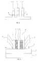
- FIG. 1is a cross-sectional view of a semiconductor wafer or device including a substrate having a pad layer, a mandrel layer where the mandrel layer is patterned to form a mandrel and a cap or mask layer formed thereon;
- FIG. 2is a cross-sectional view of the device of FIG. 1 showing the mandrels subjected to angled ion implantation processes to form doped buried layers in the mandrel;
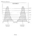
- FIG. 3is a plot of density/surface area of atoms versus target depth for arsenic to demonstrate ion ranges in accordance with the angled implantation processes
- FIG. 4is a cross-sectional view of the device of FIG. 2 showing the mandrels subjected to angled ion implantation processes to form doped surface layers in the mandrel in accordance with an alternate embodiment
- FIG. 5is a cross-sectional view of the device of FIG. 4 showing undoped layers epitaxially grown on the surface layers;
- FIG. 6is a cross-sectional view of the device of FIG. 2 or 5 showing the mandrel including an alternating doped/undoped pattern with the mask layer removed;
- FIG. 7is a cross-sectional view of the device of FIG. 6 showing the mandrel exposed to an etch process to remove the doped regions or portions to form pillars in the mandrel;
- FIG. 8is a cross-sectional view of the device of FIG. 7 showing the pillars forming a mask for processing underlying layers;
- FIG. 9is a cross-sectional view of a device showing angled ion implantation to form doped regions of different width and/or depths in accordance with an alternate embodiment
- FIG. 10is a cross-sectional view of the device of FIG. 9 showing the mandrel including an alternating doped/undoped pattern with the mask layer removed;
- FIG. 11is a cross-sectional view of the device of FIG. 10 showing the mandrel exposed to an etch process to remove the doped regions or portions to form pillars in the mandrel of different spacing and width;
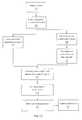
- FIG. 12is a flow diagram showing an illustrative method in accordance with the present principles.
- a multiple pattern density processhaving greater than two times the density of a single surface image transfer (SIT) process.
- SITsurface image transfer
- a triple densityis achieved in a single SIT process.
- This embodimentincludes forming an undoped mandrel on a substrate and implanting dopants into the mandrel from sidewalls to form an alternating doped-undoped pattern. The doped portion is removed selective to the undoped portion to form the triple pattern density. The pattern is then transferred into the substrate.
- the processprovides flexibility to enable the formation of patterns with different widths in the same single SIT process.
- the structure as described hereinmay be part of a design for an integrated circuit chip.
- the chip designmay be created in a graphical computer programming language, and stored in a computer storage medium (such as a disk, tape, physical hard drive, or virtual hard drive such as in a storage access network). If the designer does not fabricate chips or the photolithographic masks used to fabricate chips, the designer may transmit the resulting design by physical means (e.g., by providing a copy of the storage medium storing the design) or electronically (e.g., through the Internet) to such entities, directly or indirectly.
- the stored designis then converted into the appropriate format (e.g., GDSII) for the fabrication of photolithographic masks, which typically include multiple copies of the chip design in question that are to be formed on a wafer.
- the photolithographic masksare utilized to define areas of the wafer (and/or the layers thereon) to be etched or otherwise processed.
- the methods as described hereinmay be used in the fabrication of integrated circuit chips.
- the resulting integrated circuit chipscan be distributed by the fabricator in raw wafer form (that is, as a single wafer that has multiple unpackaged chips), as a bare die, or in a packaged form.
- the chipis mounted in a single chip package (such as a plastic carrier, with leads that are affixed to a motherboard or other higher level carrier) or in a multichip package (such as a ceramic carrier that has either or both surface interconnections or buried interconnections).
- the chipis then integrated with other chips, discrete circuit elements, and/or other signal processing devices as part of either (a) an intermediate product, such as a motherboard, or (b) an end product.
- the end productcan be any product that includes integrated circuit chips, ranging from toys and other low-end applications to advanced computer products having a display, a keyboard or other input device, and a central processor.
- a substrate 12may include a semiconductor-on-insulator substrate (SOI) having a silicon base layer with an oxide layer (BOX layer) and a silicon on oxide layer.
- SOIsemiconductor-on-insulator substrate
- BOX layeroxide layer
- the substrate 12may include any suitable material and is not limited to SOI.
- substrate 12may include gallium arsenide, monocrystalline silicon, germanium, or any other bulk material or combination of materials.
- the substrate 12further comprises other features or structures that are formed on or in the semiconductor substrate in previous process steps. Further, the present principles may be applied to interlevel dielectric layers, metal layers or any other layer and particularly when sub-minimum features sized structures are useful.
- a pad layer 16may be formed on substrate 12 .
- the pad layer 16may include an oxide (e.g., silicon dioxide), a nitride (e.g., silicon nitride) or other dielectric material. Other materials may also be employed, such as organic dielectrics, etc.
- An undoped mandrel layer 18is formed on the pad layer 16 .
- the mandrel layer 18includes polycrystalline (polysilicon) or amorphous silicon.
- a mask layer 20is formed over the mandrel layer 18 .
- the mask layer 20 and the mandrel layer 18are patterned and etched. This may include using a lithographic process that may include a resist layer (not shown) to lithographically pattern and etch the mask layer 20 .
- Resistis removed and mask layer 20 is employed as a mask to etch the mandrel layer 18 .
- the resist or other materialmay be employed to etch through the mask layer 20 and the mandrel layer 18 in a single process step. The etching forms a mandrel 22 .
- a dopant implantation processis performed. Dopants 28 and 30 are directed on an angle against sidewalls of the mandrel 22 to form an alternating doped-undoped pattern. Using angled ion implantation (I/I), doped portions 26 and undoped portions 24 of mandrel 22 are formed. Dopants 28 and 30 are introduced in a same implantation process (e.g., using a same or different sources) or may be applied in separate processes (doing one side first e.g., with dopants 28 and then the other side, e.g., with dopants 30 ). Dopant energy is controlled to accurately define the doped regions 26 .
- I/Iangled ion implantation
- Dopants 28 and 30may include phosphorus (P), arsenic (As), boron (B), indium (In), antimony (Sb), germanium (Ge), nitrogen (N), fluorine (F), carbon (C), sulfur (S), etc.
- atomsdensity over surface area
- target depthfor arsenic dopants in an illustrative plot.
- well-defined dopant distributionsare achieved which are buried in the mandrel 22 at a desired target depth.
- the target depthcan be accurately controlled based upon implantation energy, material choice (dopant material and target material) and other factors.
- doped regions 26have an etch rate that is different from undoped portions 24 .
- Angled ion implantationincludes bombarding the mask layer 20 , mandrel 22 and pad layer 16 with ions at angles of approximately 5 degrees to about 75 degrees with respect to a vertical, normal to a major surface of the device. Other angles of attack may also be employed.
- the thicknesses of pad layer 16 and mask layer 20should be large enough to protect underlying layers and structures during the implantation.
- the target depthshould be less than the thicknesses of the mask layer 20 and the pad layer 16 .
- the implant dosecan range from 1 ⁇ 10 12 /cm 2 to 5 ⁇ 10 15 /cm 2
- the implant energycan range from 0.5 KeV to 500 KeV.
- portions 26are foamed by an implantation process
- multiple buried doped layerscan be formed by multiple implantations with different implantation energies and/or angles.
- the ion implantation processis performed with less energy and results in a much shallower target depth for the ions.
- the doped portions of mandrel 22begin at the surface of the mandrel 22 .
- undoped epitaxially grown layers 36are formed on sidewalls of the mandrel 22 .
- the grown layers 36may include undoped silicon to form the same structure as provided in FIG. 2 . This structure is depicted in FIG. 6 .
- the mandrel structuresmay have doped portions 26 switched with undoped portions 24 . This can be achieved by, e.g., adjusting the implantation depths, or by, e.g., epitaxially growing doped silicon layers ( 36 ), etc.
- the epitaxial growthmay be implanted with dopants in an angled implantation process, and that the ion implantation and epitaxial processes can be repeated to form more than 2 buried doped layers.
- FIG. 6a resulting structure from FIG. 2 or FIG. 5 is depicted after the mask layer 20 has been removed. This exposes an upper portion of the doped portions 26 and the undoped portions 24 (or 30 ) so that selective etching may be performed.
- the doped portions 26are removed selective to the undoped portions 24 (and/or 30 ) to form a triple pattern density.
- the doped portions 26have an etch rate that is significantly higher than the etch rate of the undoped portions 24 (and/or 30 ).
- An etch processsuch as, a wet ammonia etch or dry etch may be employed to remove the doped regions.
- the remaining undoped portions 24 (and/or 30 )form pillars which will be employed in transferring the triple density pattern into the pad layer 16 and the substrate 12 .
- the widths of the undoped portions 24 , 30can be configured to be any size, the widths are preferably less than a minimum feature size provided by state of the art lithography techniques. In this way, device density is significantly increased. Further, spacings between the pillars (between undoped portions 24 , 30 ) may vary from larger than a minimum feature size achievable by lithography to less than a minimum feature size achievable by lithography so that sub-minimum feature sized features are fabricated.
- etchingis performed to remove unprotected areas of the pad layer 16 and to open up regions in the substrate 12 to form fins 38 or other structures.
- the etchingpreferably includes a dry etch or reactive ion etch.
- Fins 38are employed as active areas for fin field effect transistors (finFETs) which may be constructed using known processes.
- the finFETsare formed by depositing a gate dielectric and gate conductor, followed by patterning of these layers and active area implantation of dopants.
- the buried layer dopant implantationpreferably provides for three fins 38 in a same area as the conventional SIT process which only provides two.
- the processis simplified over the multiple application of the SIT process which requires many redundant and added steps.
- the present methodsprovide triple density in a single process sequence; however higher densities are also contemplated.
- the mandrel 22may be processed in a plurality of ways.
- the widths of doped portions 50 and 52 and undoped portions 44 , 46 and 48can be adjusted while forming an alternating undoped/doped pattern in the mandrel 22 .
- a triple pattern densityis formed with different pattern dimensions without adding extra process steps.
- two angled implants, one with dopants 40 and one with dopants 42have different implantation conditions such that the dimensions and positions of the doped portions 50 and 52 are varied according to a desired pattern.
- the doped portion patterndefines pillars formed for masking by the undoped portions 44 , 46 , 48 .
- the mask layer 20is stripped.
- Doped portion 52is wider than the doped portion 50 .
- portion 52is closer to a surface of the sidewall of the mandrel 22 than the doped portion 50 .
- an etch of the undoped portions 50 and 52is performed.
- the doped portions 50 and 52are etched selective to undoped portions 44 , 46 , 48 (e.g., by wet ammonia etch or dry etch).
- Three undoped portions (pillars) 44 , 46 , 48have different widths. These widths may vary from larger than a minimum feature size achievable by lithography to less than a minimum feature size achievable by lithography.
- the spacings 58 , 60 between neighboring pillars ( 44 , 46 , 48 )can be the same or different as needed.
- the spacings 58 and 60will be employed to provide the widths of underlying features. These spacings 58 and 60 may vary from larger than a minimum feature size achievable by lithography to less than a minimum feature size achievable by lithography. Processing continues from this point as described above to form finFETs, or other components.
- a flow diagram for a method for fabricating an integrated circuitis illustratively depicted.
- a mandrelis patterned over a layer to be patterned by the present method.
- a cap layer or mask layer formed on a mandrel layermay also be patterned.
- the layer to be patternedmay include a substrate and/or other layers in the semiconductor device design.
- dopantsare implanted into exposed sidewalls of the mandrel using an angled implantation process to form at least two doped layers having at least one undoped region adjacent to the doped layers.
- the implanting of dopantsmay include implanting dopants into exposed sidewalls of the mandrel using at least two angled implantation processes to form at least two buried layers in block 105 .
- the mandrelmay include amorphous silicon or polysilicon, and the dopants may include, e.g., arsenic, although other materials are also contemplated.
- a surface dopingmay be performed in block 106 to form at least one surface doped layer.
- epitaxial undoped regionsmay be grown on the at least one surface doped layer.
- Other processessuch as atomic depositions, etc. may also be employed.
- the at least two doped layersmay have at least one of different widths and different depths from a sidewall surface of the mandrel. This is achieved by adjusting dopant types, densities, target material, dopant energies, angle of implantation and/or other parameters.
- the doped layersare selectively etched away to form pillars from the undoped regions.
- the selective etching of the doped layers to form pillars from the undoped regionspreferably includes forming a three pillar structure to provide a triple pattern density structure in a single surface image transfer process sequence.
- the pillarsform a mask feature.
- the pillarsmay have a spacing of less than a minimum feature size achievable by lithography.
- the layer to be patternedis etched using the pillars as an etch mask to form features for an integrated circuit device.
- the features for the integrated circuit devicepreferably include a width of less than a minimum feature size achievable with lithography.
- the layer to be patternedis a semiconductor substrate and etching the layer to be patterned includes forming fin features for fin field effect transistor devices.
- finFETsare constructed or other devices or components are fabricated.
Landscapes
- Engineering & Computer Science (AREA)
- Physics & Mathematics (AREA)
- Condensed Matter Physics & Semiconductors (AREA)
- General Physics & Mathematics (AREA)
- Manufacturing & Machinery (AREA)
- Computer Hardware Design (AREA)
- Microelectronics & Electronic Packaging (AREA)
- Power Engineering (AREA)
- Chemical & Material Sciences (AREA)
- Inorganic Chemistry (AREA)
- Insulated Gate Type Field-Effect Transistor (AREA)
- Junction Field-Effect Transistors (AREA)
Abstract
Description
- This application is a Divisional application of co-pending U.S. patent application Ser. No. 12/628,686 filed on Dec. 1, 2009, incorporated herein by reference in its entirety.
- 1. Technical Field
- The present invention relates to semiconductor processing and more particularly to fabrication of components with density multiplication in a single process sequence.
- 2. Description of the Related Art
- Vertically disposed transistors formed on fins or fin field effect transistors (FinFETs) have been emerging as a promising new approach for continued scaling of complementary metal oxide semiconductor (CMOS) technology. Sidewall spacer imaging transfer (SIT) is one method for forming narrow fins beyond the printing capability of optical lithography. Conventional SIT methods result in a pattern density that is finer than conventional lithographic patterning techniques. However, as demand grows for increased semiconductor component density, improvements to conventional SIT methods are needed.
- In prior art processes, pattern density can be doubled by conventional sidewall imaging transfer (SIT) as described in U.S. Pat. No. 6,391,753. Another method includes performing the SIT process multiple times. While this can further increase pattern density, multiple SIT processes adds process complexity and increases process cost. For example, pattern density can be quadrupled by performing the SIT process two times, as described, e.g., in U.S. Pat. No. 6,875,703.
- A method for fabricating an integrated circuit includes patterning a mandrel over a layer to be patterned. Dopants are implanted into exposed sidewalls of the mandrel to form at least two doped layers having at least one undoped region adjacent to the doped layers. The doped layers are selectively etched away to form pillars from the undoped regions. The layer to be patterned is etched using the pillars as an etch mask to form features for an integrated circuit device.
- A method for fabricating an integrated circuit includes patterning a mandrel over a substrate, the mandrel having a mask layer formed thereon; implanting dopants into exposed sidewalls of the mandrel to form two buried layers having undoped regions adjacent to the buried layers; removing the mask layer; selectively etching away the buried layers to form pillars from the undoped regions; and etching the substrate using the pillars as an etch mask to form features for an integrated circuit device.
- Another method for fabricating an integrated circuit includes patterning a mandrel over a substrate, the mandrel having a mask layer formed thereon; implanting dopants into exposed sidewalls of the mandrel to form two surface layers having an undoped region therebetween; epitaxially growing undoped regions on two surface layers of the exposed sidewalls; removing the mask layer; selectively etching away the surface layers to form pillars from the undoped regions; and etching the substrate using the pillars as an etch mask to form features for an integrated circuit device.
- A semiconductor device includes a substrate having transistors formed thereon. The transistors have a triple density pattern such that at least three transistors are formed within a single minimum feature size achievable with lithography.
- A semiconductor device includes a substrate having transistors formed thereon. The transistors have a triple density pattern such that at least three transistors are formed within a single minimum feature size achievable with lithography, and the transistors of the triple density pattern have one of different sizes and different spacings between at least two of the three features.
- These and other features and advantages will become apparent from the following detailed description of illustrative embodiments thereof, which is to be read in connection with the accompanying drawings.
- The disclosure will provide details in the following description of preferred embodiments with reference to the following figures wherein:
FIG. 1 is a cross-sectional view of a semiconductor wafer or device including a substrate having a pad layer, a mandrel layer where the mandrel layer is patterned to form a mandrel and a cap or mask layer formed thereon;FIG. 2 is a cross-sectional view of the device ofFIG. 1 showing the mandrels subjected to angled ion implantation processes to form doped buried layers in the mandrel;FIG. 3 is a plot of density/surface area of atoms versus target depth for arsenic to demonstrate ion ranges in accordance with the angled implantation processes;FIG. 4 is a cross-sectional view of the device ofFIG. 2 showing the mandrels subjected to angled ion implantation processes to form doped surface layers in the mandrel in accordance with an alternate embodiment;FIG. 5 is a cross-sectional view of the device ofFIG. 4 showing undoped layers epitaxially grown on the surface layers;FIG. 6 is a cross-sectional view of the device ofFIG. 2 or5 showing the mandrel including an alternating doped/undoped pattern with the mask layer removed;FIG. 7 is a cross-sectional view of the device ofFIG. 6 showing the mandrel exposed to an etch process to remove the doped regions or portions to form pillars in the mandrel;FIG. 8 is a cross-sectional view of the device ofFIG. 7 showing the pillars forming a mask for processing underlying layers;FIG. 9 is a cross-sectional view of a device showing angled ion implantation to form doped regions of different width and/or depths in accordance with an alternate embodiment;FIG. 10 is a cross-sectional view of the device ofFIG. 9 showing the mandrel including an alternating doped/undoped pattern with the mask layer removed;FIG. 11 is a cross-sectional view of the device ofFIG. 10 showing the mandrel exposed to an etch process to remove the doped regions or portions to form pillars in the mandrel of different spacing and width; andFIG. 12 is a flow diagram showing an illustrative method in accordance with the present principles.- In accordance with the present principles, a multiple pattern density process is provided having greater than two times the density of a single surface image transfer (SIT) process. In one embodiment, using a SIT with multiple pattern density, a triple density is achieved in a single SIT process. This embodiment includes forming an undoped mandrel on a substrate and implanting dopants into the mandrel from sidewalls to form an alternating doped-undoped pattern. The doped portion is removed selective to the undoped portion to form the triple pattern density. The pattern is then transferred into the substrate. In addition, the process provides flexibility to enable the formation of patterns with different widths in the same single SIT process.
- It is to be understood that the present invention will be described in terms of a given illustrative architecture on a wafer; however, other architectures, structures, substrate materials and process features and steps may be varied within the scope of the present invention.
- The structure as described herein may be part of a design for an integrated circuit chip. The chip design may be created in a graphical computer programming language, and stored in a computer storage medium (such as a disk, tape, physical hard drive, or virtual hard drive such as in a storage access network). If the designer does not fabricate chips or the photolithographic masks used to fabricate chips, the designer may transmit the resulting design by physical means (e.g., by providing a copy of the storage medium storing the design) or electronically (e.g., through the Internet) to such entities, directly or indirectly. The stored design is then converted into the appropriate format (e.g., GDSII) for the fabrication of photolithographic masks, which typically include multiple copies of the chip design in question that are to be formed on a wafer. The photolithographic masks are utilized to define areas of the wafer (and/or the layers thereon) to be etched or otherwise processed.
- The methods as described herein may be used in the fabrication of integrated circuit chips. The resulting integrated circuit chips can be distributed by the fabricator in raw wafer form (that is, as a single wafer that has multiple unpackaged chips), as a bare die, or in a packaged form. In the latter case the chip is mounted in a single chip package (such as a plastic carrier, with leads that are affixed to a motherboard or other higher level carrier) or in a multichip package (such as a ceramic carrier that has either or both surface interconnections or buried interconnections). In any case, the chip is then integrated with other chips, discrete circuit elements, and/or other signal processing devices as part of either (a) an intermediate product, such as a motherboard, or (b) an end product. The end product can be any product that includes integrated circuit chips, ranging from toys and other low-end applications to advanced computer products having a display, a keyboard or other input device, and a central processor.
- Referring now to the drawings in which like numerals represent the same or similar elements and initially to
FIG. 1 , a method and structure for tripling pattern density by a single SIT process will be illustratively described. A partially fabricated structure of asemiconductor device 10 is shown. In one embodiment, asubstrate 12 may include a semiconductor-on-insulator substrate (SOI) having a silicon base layer with an oxide layer (BOX layer) and a silicon on oxide layer. It should be understood that thesubstrate 12 may include any suitable material and is not limited to SOI. For example,substrate 12 may include gallium arsenide, monocrystalline silicon, germanium, or any other bulk material or combination of materials. In some embodiments, thesubstrate 12 further comprises other features or structures that are formed on or in the semiconductor substrate in previous process steps. Further, the present principles may be applied to interlevel dielectric layers, metal layers or any other layer and particularly when sub-minimum features sized structures are useful. - A
pad layer 16 may be formed onsubstrate 12. Thepad layer 16 may include an oxide (e.g., silicon dioxide), a nitride (e.g., silicon nitride) or other dielectric material. Other materials may also be employed, such as organic dielectrics, etc. Anundoped mandrel layer 18 is formed on thepad layer 16. In one embodiment, themandrel layer 18 includes polycrystalline (polysilicon) or amorphous silicon. Amask layer 20 is formed over themandrel layer 18. Themask layer 20 and themandrel layer 18 are patterned and etched. This may include using a lithographic process that may include a resist layer (not shown) to lithographically pattern and etch themask layer 20. Resist is removed andmask layer 20 is employed as a mask to etch themandrel layer 18. In other embodiments, the resist or other material may be employed to etch through themask layer 20 and themandrel layer 18 in a single process step. The etching forms amandrel 22. - Referring to
FIG. 2 , a dopant implantation process is performed. Dopants28 and30 are directed on an angle against sidewalls of themandrel 22 to form an alternating doped-undoped pattern. Using angled ion implantation (I/I), dopedportions 26 andundoped portions 24 ofmandrel 22 are formed. Dopants28 and30 are introduced in a same implantation process (e.g., using a same or different sources) or may be applied in separate processes (doing one side first e.g., withdopants 28 and then the other side, e.g., with dopants30). Dopant energy is controlled to accurately define the dopedregions 26. Dopants28 and30 may include phosphorus (P), arsenic (As), boron (B), indium (In), antimony (Sb), germanium (Ge), nitrogen (N), fluorine (F), carbon (C), sulfur (S), etc. - Referring to
FIG. 3 , atoms (density over surface area) are plotted verses target depth for arsenic dopants in an illustrative plot. As can be seen fromFIG. 3 , well-defined dopant distributions are achieved which are buried in themandrel 22 at a desired target depth. The target depth can be accurately controlled based upon implantation energy, material choice (dopant material and target material) and other factors. - Referring again to
FIG. 2 , as a result of the implantation process,doped regions 26 have an etch rate that is different fromundoped portions 24. Angled ion implantation includes bombarding themask layer 20,mandrel 22 andpad layer 16 with ions at angles of approximately 5 degrees to about 75 degrees with respect to a vertical, normal to a major surface of the device. Other angles of attack may also be employed. It should be noted that the thicknesses ofpad layer 16 andmask layer 20 should be large enough to protect underlying layers and structures during the implantation. For example, the target depth should be less than the thicknesses of themask layer 20 and thepad layer 16. Depending on the target depth and implant species, the implant dose can range from 1×10¹²/cm2to 5×10¹⁵/cm2, the implant energy can range from 0.5 KeV to 500 KeV. - Although two buried doped layers (portions26) are foamed by an implantation process, multiple buried doped layers (more than 2) can be formed by multiple implantations with different implantation energies and/or angles.
- Referring to
FIG. 4 , in an alternate embodiment, the ion implantation process is performed with less energy and results in a much shallower target depth for the ions. In one embodiment, the doped portions ofmandrel 22 begin at the surface of themandrel 22. - Referring to
FIG. 5 , undoped epitaxially grown layers36 are formed on sidewalls of themandrel 22. The grown layers36 may include undoped silicon to form the same structure as provided inFIG. 2 . This structure is depicted inFIG. 6 . Note that in other embodiments, the mandrel structures may have dopedportions 26 switched withundoped portions 24. This can be achieved by, e.g., adjusting the implantation depths, or by, e.g., epitaxially growing doped silicon layers (36), etc. Note that the epitaxial growth may be implanted with dopants in an angled implantation process, and that the ion implantation and epitaxial processes can be repeated to form more than 2 buried doped layers. - Referring to
FIG. 6 , a resulting structure fromFIG. 2 orFIG. 5 is depicted after themask layer 20 has been removed. This exposes an upper portion of the dopedportions 26 and the undoped portions24 (or30) so that selective etching may be performed. - Referring to
FIG. 7 , the dopedportions 26 are removed selective to the undoped portions24 (and/or30) to form a triple pattern density. Thedoped portions 26 have an etch rate that is significantly higher than the etch rate of the undoped portions24 (and/or30). An etch process, such as, a wet ammonia etch or dry etch may be employed to remove the doped regions. The remaining undoped portions24 (and/or30) form pillars which will be employed in transferring the triple density pattern into thepad layer 16 and thesubstrate 12. - It should be understood that while the widths of the
undoped portions undoped portions 24,30) may vary from larger than a minimum feature size achievable by lithography to less than a minimum feature size achievable by lithography so that sub-minimum feature sized features are fabricated. - Referring to
FIG. 8 , using the undoped portions24 (and/or30) as a mask, etching is performed to remove unprotected areas of thepad layer 16 and to open up regions in thesubstrate 12 to formfins 38 or other structures. The etching preferably includes a dry etch or reactive ion etch.Fins 38 are employed as active areas for fin field effect transistors (finFETs) which may be constructed using known processes. The finFETs are formed by depositing a gate dielectric and gate conductor, followed by patterning of these layers and active area implantation of dopants. - The buried layer dopant implantation preferably provides for three
fins 38 in a same area as the conventional SIT process which only provides two. In addition, the process is simplified over the multiple application of the SIT process which requires many redundant and added steps. The present methods provide triple density in a single process sequence; however higher densities are also contemplated. - Referring to
FIG. 9 , in an alternate embodiment, themandrel 22 may be processed in a plurality of ways. In one embodiment, the widths of dopedportions undoped portions mandrel 22. In the example ofFIG. 9 , a triple pattern density is formed with different pattern dimensions without adding extra process steps. In this embodiment, two angled implants, one withdopants 40 and one withdopants 42 have different implantation conditions such that the dimensions and positions of the dopedportions undoped portions - Referring to
FIG. 10 , themask layer 20 is stripped. Dopedportion 52 is wider than the dopedportion 50. In addition,portion 52 is closer to a surface of the sidewall of themandrel 22 than the dopedportion 50. - Referring to
FIG. 11 , an etch of theundoped portions portions undoped portions spacings spacings spacings - Referring to
FIG. 12 , a flow diagram for a method for fabricating an integrated circuit is illustratively depicted. Inblock 102, a mandrel is patterned over a layer to be patterned by the present method. A cap layer or mask layer formed on a mandrel layer may also be patterned. The layer to be patterned may include a substrate and/or other layers in the semiconductor device design. - In
block 104, dopants are implanted into exposed sidewalls of the mandrel using an angled implantation process to form at least two doped layers having at least one undoped region adjacent to the doped layers. The implanting of dopants may include implanting dopants into exposed sidewalls of the mandrel using at least two angled implantation processes to form at least two buried layers inblock 105. The mandrel may include amorphous silicon or polysilicon, and the dopants may include, e.g., arsenic, although other materials are also contemplated. - In an alternate embodiment, a surface doping may be performed in
block 106 to form at least one surface doped layer. In block107, epitaxial undoped regions may be grown on the at least one surface doped layer. Other processes such as atomic depositions, etc. may also be employed. - In block108, the at least two doped layers may have at least one of different widths and different depths from a sidewall surface of the mandrel. This is achieved by adjusting dopant types, densities, target material, dopant energies, angle of implantation and/or other parameters.
- In
block 110, the doped layers are selectively etched away to form pillars from the undoped regions. The selective etching of the doped layers to form pillars from the undoped regions preferably includes forming a three pillar structure to provide a triple pattern density structure in a single surface image transfer process sequence. The pillars form a mask feature. The pillars may have a spacing of less than a minimum feature size achievable by lithography. - In
block 112, the layer to be patterned is etched using the pillars as an etch mask to form features for an integrated circuit device. The features for the integrated circuit device preferably include a width of less than a minimum feature size achievable with lithography. In one embodiment, the layer to be patterned is a semiconductor substrate and etching the layer to be patterned includes forming fin features for fin field effect transistor devices. - In
block 114, further processing is performed. For example, finFETs are constructed or other devices or components are fabricated. - Having described preferred embodiments for multiplying pattern density by single sidewall imaging transfer (which are intended to be illustrative and not limiting), it is noted that modifications and variations can be made by persons skilled in the art in light of the above teachings. It is therefore to be understood that changes may be made in the particular embodiments disclosed which are within the scope of the invention as outlined by the appended claims. Having thus described aspects of the invention, with the details and particularity required by the patent laws, what is claimed and desired protected by Letters Patent is set forth in the appended claims.
Claims (9)
Priority Applications (1)
| Application Number | Priority Date | Filing Date | Title |
|---|---|---|---|
| US13/552,205US8525235B2 (en) | 2009-12-01 | 2012-07-18 | Multiplying pattern density by single sidewall imaging transfer |
Applications Claiming Priority (2)
| Application Number | Priority Date | Filing Date | Title |
|---|---|---|---|
| US12/628,686US8354331B2 (en) | 2009-12-01 | 2009-12-01 | Multiplying pattern density by single sidewall imaging transfer |
| US13/552,205US8525235B2 (en) | 2009-12-01 | 2012-07-18 | Multiplying pattern density by single sidewall imaging transfer |
Related Parent Applications (1)
| Application Number | Title | Priority Date | Filing Date |
|---|---|---|---|
| US12/628,686DivisionUS8354331B2 (en) | 2009-12-01 | 2009-12-01 | Multiplying pattern density by single sidewall imaging transfer |
Publications (2)
| Publication Number | Publication Date |
|---|---|
| US20120280283A1true US20120280283A1 (en) | 2012-11-08 |
| US8525235B2 US8525235B2 (en) | 2013-09-03 |
Family
ID=44068195
Family Applications (2)
| Application Number | Title | Priority Date | Filing Date |
|---|---|---|---|
| US12/628,686Expired - Fee RelatedUS8354331B2 (en) | 2009-12-01 | 2009-12-01 | Multiplying pattern density by single sidewall imaging transfer |
| US13/552,205Expired - Fee RelatedUS8525235B2 (en) | 2009-12-01 | 2012-07-18 | Multiplying pattern density by single sidewall imaging transfer |
Family Applications Before (1)
| Application Number | Title | Priority Date | Filing Date |
|---|---|---|---|
| US12/628,686Expired - Fee RelatedUS8354331B2 (en) | 2009-12-01 | 2009-12-01 | Multiplying pattern density by single sidewall imaging transfer |
Country Status (1)
| Country | Link |
|---|---|
| US (2) | US8354331B2 (en) |
Cited By (3)
| Publication number | Priority date | Publication date | Assignee | Title |
|---|---|---|---|---|
| US9040371B2 (en) | 2013-08-07 | 2015-05-26 | International Business Machines Corporation | Integration of dense and variable pitch fin structures |
| US9064901B1 (en) | 2013-12-23 | 2015-06-23 | International Business Machines Corporation | Fin density control of multigate devices through sidewall image transfer processes |
| US9099401B2 (en) | 2013-08-16 | 2015-08-04 | International Business Machines Corporation | Sidewall image transfer with a spin-on hardmask |
Families Citing this family (27)
| Publication number | Priority date | Publication date | Assignee | Title |
|---|---|---|---|---|
| US8853092B2 (en)* | 2011-12-30 | 2014-10-07 | Taiwan Semiconductor Manufacturing Company, Ltd. | Self-aligned patterning with implantation |
| US9123654B2 (en) | 2013-02-15 | 2015-09-01 | International Business Machines Corporation | Trilayer SIT process with transfer layer for FINFET patterning |
| US8951870B2 (en)* | 2013-03-14 | 2015-02-10 | International Business Machines Corporation | Forming strained and relaxed silicon and silicon germanium fins on the same wafer |
| US9564312B2 (en) | 2014-11-24 | 2017-02-07 | Lam Research Corporation | Selective inhibition in atomic layer deposition of silicon-containing films |
| US9601693B1 (en) | 2015-09-24 | 2017-03-21 | Lam Research Corporation | Method for encapsulating a chalcogenide material |
| US10121879B2 (en) | 2015-09-28 | 2018-11-06 | International Business Machines Corporation | Forming odd number of fins by sidewall imaging transfer |
| US9852917B2 (en)* | 2016-03-22 | 2017-12-26 | International Business Machines Corporation | Methods of fabricating semiconductor fins by double sidewall image transfer patterning through localized oxidation enhancement of sacrificial mandrel sidewalls |
| US9773870B1 (en) | 2016-06-28 | 2017-09-26 | International Business Machines Corporation | Strained semiconductor device |
| US9882028B2 (en) | 2016-06-29 | 2018-01-30 | International Business Machines Corporation | Pitch split patterning for semiconductor devices |
| US10629435B2 (en)* | 2016-07-29 | 2020-04-21 | Lam Research Corporation | Doped ALD films for semiconductor patterning applications |
| US10074543B2 (en) | 2016-08-31 | 2018-09-11 | Lam Research Corporation | High dry etch rate materials for semiconductor patterning applications |
| US9997369B2 (en) | 2016-09-27 | 2018-06-12 | International Business Machines Corporation | Margin for fin cut using self-aligned triple patterning |
| US10832908B2 (en) | 2016-11-11 | 2020-11-10 | Lam Research Corporation | Self-aligned multi-patterning process flow with ALD gapfill spacer mask |
| US10454029B2 (en) | 2016-11-11 | 2019-10-22 | Lam Research Corporation | Method for reducing the wet etch rate of a sin film without damaging the underlying substrate |
| US10134579B2 (en) | 2016-11-14 | 2018-11-20 | Lam Research Corporation | Method for high modulus ALD SiO2 spacer |
| US20200066521A1 (en)* | 2017-03-31 | 2020-02-27 | Intel Corporation | Colored self-aligned subtractive patterning |
| US10325777B2 (en) | 2017-08-30 | 2019-06-18 | International Business Machines Corporation | Utilizing multiple layers to increase spatial frequency |
| US10269559B2 (en) | 2017-09-13 | 2019-04-23 | Lam Research Corporation | Dielectric gapfill of high aspect ratio features utilizing a sacrificial etch cap layer |
| CN107863318B (en)* | 2017-11-22 | 2024-05-17 | 长鑫存储技术有限公司 | Integrated circuit pattern formed based on pitch multiplication and forming method |
| CN112005343B (en) | 2018-03-02 | 2025-05-06 | 朗姆研究公司 | Selective deposition using hydrolysis |
| US10629436B2 (en) | 2018-04-12 | 2020-04-21 | International Business Machines Corporation | Spacer image transfer with double mandrel |
| KR102608900B1 (en) | 2018-07-30 | 2023-12-07 | 삼성전자주식회사 | Method of Manufacturing Semiconductor Device |
| CN111370309B (en)* | 2018-12-26 | 2023-12-12 | 中芯国际集成电路制造(上海)有限公司 | Semiconductor structure and forming method thereof |
| CN111640656B (en)* | 2019-03-01 | 2023-06-09 | 中芯国际集成电路制造(上海)有限公司 | Semiconductor device and method of forming the same |
| KR102837863B1 (en) | 2019-06-04 | 2025-07-23 | 램 리써치 코포레이션 | Polymeric protective liner for reactive ion etching during patterning |
| CN114207184A (en) | 2019-08-06 | 2022-03-18 | 朗姆研究公司 | Thermal Atomic Layer Deposition of Silicon-Containing Films |
| CN115735261A (en) | 2020-07-28 | 2023-03-03 | 朗姆研究公司 | Impurity reduction in silicon-containing films |
Citations (9)
| Publication number | Priority date | Publication date | Assignee | Title |
|---|---|---|---|---|
| US20010012215A1 (en)* | 1999-12-22 | 2001-08-09 | Toshiharu Furukawa | Multi-level dram trench store utilizing two capacitors and two plates |
| US6365059B1 (en)* | 2000-04-28 | 2002-04-02 | Alexander Pechenik | Method for making a nano-stamp and for forming, with the stamp, nano-size elements on a substrate |
| US20060051946A1 (en)* | 2004-08-31 | 2006-03-09 | Stmicroelectronics S.R.L. | Method for realizing a hosting structure of nanometric elements |
| US20060163690A1 (en)* | 2003-12-19 | 2006-07-27 | Third Dimension (3D) Semiconductor, Inc. | Semiconductor having thick dielectric regions |
| US20060205174A1 (en)* | 2003-12-19 | 2006-09-14 | Third Dimension (3D) Semiconductor, Inc. | Method for Manufacturing a Superjunction Device With Wide Mesas |
| US20060273456A1 (en)* | 2005-06-02 | 2006-12-07 | Micron Technology, Inc., A Corporation | Multiple spacer steps for pitch multiplication |
| US7662299B2 (en)* | 2005-08-30 | 2010-02-16 | Micron Technology, Inc. | Nanoimprint lithography template techniques for use during the fabrication of a semiconductor device and systems including same |
| US7696101B2 (en)* | 2005-11-01 | 2010-04-13 | Micron Technology, Inc. | Process for increasing feature density during the manufacture of a semiconductor device |
| US7807575B2 (en)* | 2006-11-29 | 2010-10-05 | Micron Technology, Inc. | Methods to reduce the critical dimension of semiconductor devices |
Family Cites Families (4)
| Publication number | Priority date | Publication date | Assignee | Title |
|---|---|---|---|---|
| US6391753B1 (en) | 2000-06-20 | 2002-05-21 | Advanced Micro Devices, Inc. | Process for forming gate conductors |
| JP3993458B2 (en)* | 2002-04-17 | 2007-10-17 | 株式会社東芝 | Semiconductor device |
| US6875703B1 (en) | 2004-01-20 | 2005-04-05 | International Business Machines Corporation | Method for forming quadruple density sidewall image transfer (SIT) structures |
| US7611980B2 (en)* | 2006-08-30 | 2009-11-03 | Micron Technology, Inc. | Single spacer process for multiplying pitch by a factor greater than two and related intermediate IC structures |
- 2009
- 2009-12-01USUS12/628,686patent/US8354331B2/ennot_activeExpired - Fee Related
- 2012
- 2012-07-18USUS13/552,205patent/US8525235B2/ennot_activeExpired - Fee Related
Patent Citations (10)
| Publication number | Priority date | Publication date | Assignee | Title |
|---|---|---|---|---|
| US20010012215A1 (en)* | 1999-12-22 | 2001-08-09 | Toshiharu Furukawa | Multi-level dram trench store utilizing two capacitors and two plates |
| US6365059B1 (en)* | 2000-04-28 | 2002-04-02 | Alexander Pechenik | Method for making a nano-stamp and for forming, with the stamp, nano-size elements on a substrate |
| US20060163690A1 (en)* | 2003-12-19 | 2006-07-27 | Third Dimension (3D) Semiconductor, Inc. | Semiconductor having thick dielectric regions |
| US20060205174A1 (en)* | 2003-12-19 | 2006-09-14 | Third Dimension (3D) Semiconductor, Inc. | Method for Manufacturing a Superjunction Device With Wide Mesas |
| US20060051946A1 (en)* | 2004-08-31 | 2006-03-09 | Stmicroelectronics S.R.L. | Method for realizing a hosting structure of nanometric elements |
| US20060273456A1 (en)* | 2005-06-02 | 2006-12-07 | Micron Technology, Inc., A Corporation | Multiple spacer steps for pitch multiplication |
| US7560390B2 (en)* | 2005-06-02 | 2009-07-14 | Micron Technology, Inc. | Multiple spacer steps for pitch multiplication |
| US7662299B2 (en)* | 2005-08-30 | 2010-02-16 | Micron Technology, Inc. | Nanoimprint lithography template techniques for use during the fabrication of a semiconductor device and systems including same |
| US7696101B2 (en)* | 2005-11-01 | 2010-04-13 | Micron Technology, Inc. | Process for increasing feature density during the manufacture of a semiconductor device |
| US7807575B2 (en)* | 2006-11-29 | 2010-10-05 | Micron Technology, Inc. | Methods to reduce the critical dimension of semiconductor devices |
Cited By (8)
| Publication number | Priority date | Publication date | Assignee | Title |
|---|---|---|---|---|
| US9040371B2 (en) | 2013-08-07 | 2015-05-26 | International Business Machines Corporation | Integration of dense and variable pitch fin structures |
| US9087792B2 (en) | 2013-08-07 | 2015-07-21 | International Business Machines Corporation | Integration of dense and variable pitch fin structures |
| US9378972B2 (en) | 2013-08-07 | 2016-06-28 | Globalfoundries Inc. | Integration of dense and variable pitch fin structures |
| US9099401B2 (en) | 2013-08-16 | 2015-08-04 | International Business Machines Corporation | Sidewall image transfer with a spin-on hardmask |
| US9293345B2 (en) | 2013-08-16 | 2016-03-22 | Globalfoundries Inc. | Sidewall image transfer with a spin-on hardmask |
| US9064901B1 (en) | 2013-12-23 | 2015-06-23 | International Business Machines Corporation | Fin density control of multigate devices through sidewall image transfer processes |
| US9728419B2 (en) | 2013-12-23 | 2017-08-08 | International Business Machines Corporation | Fin density control of multigate devices through sidewall image transfer processes |
| US10170327B2 (en) | 2013-12-23 | 2019-01-01 | International Business Machines Corporation | Fin density control of multigate devices through sidewall image transfer processes |
Also Published As
| Publication number | Publication date |
|---|---|
| US8525235B2 (en) | 2013-09-03 |
| US8354331B2 (en) | 2013-01-15 |
| US20110127582A1 (en) | 2011-06-02 |
Similar Documents
| Publication | Publication Date | Title |
|---|---|---|
| US8525235B2 (en) | Multiplying pattern density by single sidewall imaging transfer | |
| US8105901B2 (en) | Method for double pattern density | |
| US11581190B2 (en) | Method of fabricating semiconductor fins by differentially oxidizing mandrel sidewalls | |
| US8021949B2 (en) | Method and structure for forming finFETs with multiple doping regions on a same chip | |
| US6642090B1 (en) | Fin FET devices from bulk semiconductor and method for forming | |
| US9508850B2 (en) | Epitaxial block layer for a fin field effect transistor device | |
| US20120032267A1 (en) | Device and method for uniform sti recess | |
| US9236269B2 (en) | Field effect transistor (FinFET) device with a planar block area to enable variable Fin pitch and width | |
| US9231085B2 (en) | Semiconductor structure and methods of manufacture | |
| US10943989B2 (en) | Gate to source/drain leakage reduction in nanosheet transistors via inner spacer optimization | |
| CN103117243A (en) | Reverse tone STI formation | |
| US8343877B2 (en) | Angle ion implant to re-shape sidewall image transfer patterns | |
| US20150162435A1 (en) | Asymmetric channel growth of a cladding layer over fins of a field effect transistor (finfet) device | |
| US9761594B2 (en) | Hardmask for a halo/extension implant of a static random access memory (SRAM) layout | |
| US10879068B2 (en) | Extreme ultraviolet lithography for high volume manufacture of a semiconductor device | |
| US9087772B2 (en) | Device and method for forming sharp extension region with controllable junction depth and lateral overlap | |
| US12176212B2 (en) | Mandrel structures and methods of fabricating the same in semiconductor devices | |
| US10685866B2 (en) | Fin isolation to mitigate local layout effects |
Legal Events
| Date | Code | Title | Description |
|---|---|---|---|
| STCF | Information on status: patent grant | Free format text:PATENTED CASE | |
| AS | Assignment | Owner name:GLOBALFOUNDRIES U.S. 2 LLC, NEW YORK Free format text:ASSIGNMENT OF ASSIGNORS INTEREST;ASSIGNOR:INTERNATIONAL BUSINESS MACHINES CORPORATION;REEL/FRAME:036550/0001 Effective date:20150629 | |
| AS | Assignment | Owner name:GLOBALFOUNDRIES INC., CAYMAN ISLANDS Free format text:ASSIGNMENT OF ASSIGNORS INTEREST;ASSIGNORS:GLOBALFOUNDRIES U.S. 2 LLC;GLOBALFOUNDRIES U.S. INC.;REEL/FRAME:036779/0001 Effective date:20150910 | |
| FPAY | Fee payment | Year of fee payment:4 | |
| AS | Assignment | Owner name:WILMINGTON TRUST, NATIONAL ASSOCIATION, DELAWARE Free format text:SECURITY AGREEMENT;ASSIGNOR:GLOBALFOUNDRIES INC.;REEL/FRAME:049490/0001 Effective date:20181127 | |
| AS | Assignment | Owner name:GLOBALFOUNDRIES U.S. INC., CALIFORNIA Free format text:ASSIGNMENT OF ASSIGNORS INTEREST;ASSIGNOR:GLOBALFOUNDRIES INC.;REEL/FRAME:054633/0001 Effective date:20201022 | |
| AS | Assignment | Owner name:GLOBALFOUNDRIES INC., CAYMAN ISLANDS Free format text:RELEASE BY SECURED PARTY;ASSIGNOR:WILMINGTON TRUST, NATIONAL ASSOCIATION;REEL/FRAME:054636/0001 Effective date:20201117 | |
| MAFP | Maintenance fee payment | Free format text:PAYMENT OF MAINTENANCE FEE, 8TH YEAR, LARGE ENTITY (ORIGINAL EVENT CODE: M1552); ENTITY STATUS OF PATENT OWNER: LARGE ENTITY Year of fee payment:8 | |
| AS | Assignment | Owner name:GLOBALFOUNDRIES U.S. INC., NEW YORK Free format text:RELEASE BY SECURED PARTY;ASSIGNOR:WILMINGTON TRUST, NATIONAL ASSOCIATION;REEL/FRAME:056987/0001 Effective date:20201117 | |
| FEPP | Fee payment procedure | Free format text:MAINTENANCE FEE REMINDER MAILED (ORIGINAL EVENT CODE: REM.); ENTITY STATUS OF PATENT OWNER: LARGE ENTITY | |
| LAPS | Lapse for failure to pay maintenance fees | Free format text:PATENT EXPIRED FOR FAILURE TO PAY MAINTENANCE FEES (ORIGINAL EVENT CODE: EXP.); ENTITY STATUS OF PATENT OWNER: LARGE ENTITY | |
| STCH | Information on status: patent discontinuation | Free format text:PATENT EXPIRED DUE TO NONPAYMENT OF MAINTENANCE FEES UNDER 37 CFR 1.362 |