US20120269967A1 - Hot Wire Atomic Layer Deposition Apparatus And Methods Of Use - Google Patents
Hot Wire Atomic Layer Deposition Apparatus And Methods Of UseDownload PDFInfo
- Publication number
- US20120269967A1 US20120269967A1US13/437,567US201213437567AUS2012269967A1US 20120269967 A1US20120269967 A1US 20120269967A1US 201213437567 AUS201213437567 AUS 201213437567AUS 2012269967 A1US2012269967 A1US 2012269967A1
- Authority
- US
- United States
- Prior art keywords
- precursor gas
- gas
- wire
- precursor
- distribution plate
- Prior art date
- Legal status (The legal status is an assumption and is not a legal conclusion. Google has not performed a legal analysis and makes no representation as to the accuracy of the status listed.)
- Abandoned
Links
Images


Classifications
- C—CHEMISTRY; METALLURGY
- C23—COATING METALLIC MATERIAL; COATING MATERIAL WITH METALLIC MATERIAL; CHEMICAL SURFACE TREATMENT; DIFFUSION TREATMENT OF METALLIC MATERIAL; COATING BY VACUUM EVAPORATION, BY SPUTTERING, BY ION IMPLANTATION OR BY CHEMICAL VAPOUR DEPOSITION, IN GENERAL; INHIBITING CORROSION OF METALLIC MATERIAL OR INCRUSTATION IN GENERAL
- C23C—COATING METALLIC MATERIAL; COATING MATERIAL WITH METALLIC MATERIAL; SURFACE TREATMENT OF METALLIC MATERIAL BY DIFFUSION INTO THE SURFACE, BY CHEMICAL CONVERSION OR SUBSTITUTION; COATING BY VACUUM EVAPORATION, BY SPUTTERING, BY ION IMPLANTATION OR BY CHEMICAL VAPOUR DEPOSITION, IN GENERAL
- C23C16/00—Chemical coating by decomposition of gaseous compounds, without leaving reaction products of surface material in the coating, i.e. chemical vapour deposition [CVD] processes
- C23C16/44—Chemical coating by decomposition of gaseous compounds, without leaving reaction products of surface material in the coating, i.e. chemical vapour deposition [CVD] processes characterised by the method of coating
- C23C16/455—Chemical coating by decomposition of gaseous compounds, without leaving reaction products of surface material in the coating, i.e. chemical vapour deposition [CVD] processes characterised by the method of coating characterised by the method used for introducing gases into reaction chamber or for modifying gas flows in reaction chamber
- C23C16/45523—Pulsed gas flow or change of composition over time
- C23C16/45525—Atomic layer deposition [ALD]
- C23C16/45544—Atomic layer deposition [ALD] characterized by the apparatus
- C23C16/45548—Atomic layer deposition [ALD] characterized by the apparatus having arrangements for gas injection at different locations of the reactor for each ALD half-reaction
- C23C16/45551—Atomic layer deposition [ALD] characterized by the apparatus having arrangements for gas injection at different locations of the reactor for each ALD half-reaction for relative movement of the substrate and the gas injectors or half-reaction reactor compartments
- C—CHEMISTRY; METALLURGY
- C23—COATING METALLIC MATERIAL; COATING MATERIAL WITH METALLIC MATERIAL; CHEMICAL SURFACE TREATMENT; DIFFUSION TREATMENT OF METALLIC MATERIAL; COATING BY VACUUM EVAPORATION, BY SPUTTERING, BY ION IMPLANTATION OR BY CHEMICAL VAPOUR DEPOSITION, IN GENERAL; INHIBITING CORROSION OF METALLIC MATERIAL OR INCRUSTATION IN GENERAL
- C23C—COATING METALLIC MATERIAL; COATING MATERIAL WITH METALLIC MATERIAL; SURFACE TREATMENT OF METALLIC MATERIAL BY DIFFUSION INTO THE SURFACE, BY CHEMICAL CONVERSION OR SUBSTITUTION; COATING BY VACUUM EVAPORATION, BY SPUTTERING, BY ION IMPLANTATION OR BY CHEMICAL VAPOUR DEPOSITION, IN GENERAL
- C23C16/00—Chemical coating by decomposition of gaseous compounds, without leaving reaction products of surface material in the coating, i.e. chemical vapour deposition [CVD] processes
- C23C16/44—Chemical coating by decomposition of gaseous compounds, without leaving reaction products of surface material in the coating, i.e. chemical vapour deposition [CVD] processes characterised by the method of coating
- C23C16/448—Chemical coating by decomposition of gaseous compounds, without leaving reaction products of surface material in the coating, i.e. chemical vapour deposition [CVD] processes characterised by the method of coating characterised by the method used for generating reactive gas streams, e.g. by evaporation or sublimation of precursor materials
- C23C16/452—Chemical coating by decomposition of gaseous compounds, without leaving reaction products of surface material in the coating, i.e. chemical vapour deposition [CVD] processes characterised by the method of coating characterised by the method used for generating reactive gas streams, e.g. by evaporation or sublimation of precursor materials by activating reactive gas streams before their introduction into the reaction chamber, e.g. by ionisation or addition of reactive species
- C—CHEMISTRY; METALLURGY
- C23—COATING METALLIC MATERIAL; COATING MATERIAL WITH METALLIC MATERIAL; CHEMICAL SURFACE TREATMENT; DIFFUSION TREATMENT OF METALLIC MATERIAL; COATING BY VACUUM EVAPORATION, BY SPUTTERING, BY ION IMPLANTATION OR BY CHEMICAL VAPOUR DEPOSITION, IN GENERAL; INHIBITING CORROSION OF METALLIC MATERIAL OR INCRUSTATION IN GENERAL
- C23C—COATING METALLIC MATERIAL; COATING MATERIAL WITH METALLIC MATERIAL; SURFACE TREATMENT OF METALLIC MATERIAL BY DIFFUSION INTO THE SURFACE, BY CHEMICAL CONVERSION OR SUBSTITUTION; COATING BY VACUUM EVAPORATION, BY SPUTTERING, BY ION IMPLANTATION OR BY CHEMICAL VAPOUR DEPOSITION, IN GENERAL
- C23C16/00—Chemical coating by decomposition of gaseous compounds, without leaving reaction products of surface material in the coating, i.e. chemical vapour deposition [CVD] processes
- C23C16/44—Chemical coating by decomposition of gaseous compounds, without leaving reaction products of surface material in the coating, i.e. chemical vapour deposition [CVD] processes characterised by the method of coating
- C23C16/455—Chemical coating by decomposition of gaseous compounds, without leaving reaction products of surface material in the coating, i.e. chemical vapour deposition [CVD] processes characterised by the method of coating characterised by the method used for introducing gases into reaction chamber or for modifying gas flows in reaction chamber
- C23C16/45523—Pulsed gas flow or change of composition over time
- C23C16/45525—Atomic layer deposition [ALD]
- C23C16/45544—Atomic layer deposition [ALD] characterized by the apparatus
- C—CHEMISTRY; METALLURGY
- C23—COATING METALLIC MATERIAL; COATING MATERIAL WITH METALLIC MATERIAL; CHEMICAL SURFACE TREATMENT; DIFFUSION TREATMENT OF METALLIC MATERIAL; COATING BY VACUUM EVAPORATION, BY SPUTTERING, BY ION IMPLANTATION OR BY CHEMICAL VAPOUR DEPOSITION, IN GENERAL; INHIBITING CORROSION OF METALLIC MATERIAL OR INCRUSTATION IN GENERAL
- C23C—COATING METALLIC MATERIAL; COATING MATERIAL WITH METALLIC MATERIAL; SURFACE TREATMENT OF METALLIC MATERIAL BY DIFFUSION INTO THE SURFACE, BY CHEMICAL CONVERSION OR SUBSTITUTION; COATING BY VACUUM EVAPORATION, BY SPUTTERING, BY ION IMPLANTATION OR BY CHEMICAL VAPOUR DEPOSITION, IN GENERAL
- C23C16/00—Chemical coating by decomposition of gaseous compounds, without leaving reaction products of surface material in the coating, i.e. chemical vapour deposition [CVD] processes
- C23C16/44—Chemical coating by decomposition of gaseous compounds, without leaving reaction products of surface material in the coating, i.e. chemical vapour deposition [CVD] processes characterised by the method of coating
- C23C16/455—Chemical coating by decomposition of gaseous compounds, without leaving reaction products of surface material in the coating, i.e. chemical vapour deposition [CVD] processes characterised by the method of coating characterised by the method used for introducing gases into reaction chamber or for modifying gas flows in reaction chamber
- C23C16/45563—Gas nozzles
Definitions
- Embodiments of the inventiongenerally relate to an apparatus and a method for depositing materials. More specifically, embodiments of the invention are directed to a atomic layer deposition chambers with a hot wire for exciting gaseous species before contacting the substrate surface.
- vapor deposition processeshave played an important role in depositing materials on substrates.
- the size and aspect ratio of the featuresare becoming more aggressive, e.g., feature sizes of 0.07 ⁇ m and aspect ratios of 10 or greater. Accordingly, conformal deposition of materials to form these devices is becoming increasingly important.
- ALDatomic layer deposition
- reactant gasesare sequentially introduced into a process chamber containing a substrate.
- a first reactantis introduced into a process chamber and is adsorbed onto the substrate surface.
- a second reactantis then introduced into the process chamber and reacts with the first reactant to form a deposited material.
- a purge stepmay be carried out between the delivery of each reactant gas to ensure that the only reactions that occur are on the substrate surface.
- the purge stepmay be a continuous purge with a carrier gas or a pulse purge between the delivery of the reactant gases.
- Embodiments of the inventionare directed to gas distribution plates comprising an input face, an output face and a wire.
- the input facecomprises a first precursor gas input configured to receive a flow of a first precursor gas and a second precursor gas input configured to receive a flow of a second precursor gas.
- the output facehas a plurality of elongate gas ports configured to direct flows of gases toward a substrate adjacent the output face.
- the elongate gas portsinclude at least one first precursor gas port and at least one second precursor gas port.
- the at least one first precursor gas portis in flow communication with the first precursor gas and the at least one second precursor gas port in flow communication with the second precursor gas.
- the wireis positioned within at least one of the first precursor gas port and the second precursor gas port and is connected to a power source to heat the wire.
- the wirecomprises tungsten.
- the wirecan be heated to excite species in a gas flowing across the wire.
- the gas distribution platefurther comprises a tensioner connected to the wire to provide a tension.
- the tensionercomprises a spring.
- the tensionis sufficient to prevent significant sagging in the wire and breakage of the wire.
- the tensioneris attached to the input face of the gas distribution plate.
- the wireis within an enclosure attached to the output face and positioned so that gases exiting one or more of the first precursor gas port and the second precursor gas port pas through the enclosure.
- the plurality of elongate gas portsconsist essentially of, in order, a leading first precursor gas port, a second precursor gas port and a trailing first precursor gas port.
- the wireis a single wire extending along both first precursor gas ports and wrapping around the second precursor gas port.
- the wireextends along the at least one second precursor gas port.
- the plurality of elongate gas portsconsist essentially of, in order, at least two repeating units of alternating first precursor gas ports and second precursor gas ports followed by a trailing first precursor gas port.
- the wireextends along each of the first precursor gas ports. In specific embodiments, the wire extends along each of the second precursor gas ports.
- Additional embodiments of the inventionare directed to processing chambers with the gas distribution plate described.
- FIG. 1A substrate having a surface is laterally moved beneath a gas distribution plate comprising a plurality of elongate gas ports including at least one first precursor gas port configured to deliver a first precursor gas and at least one second precursor gas port configured to deliver a second precursor gas.
- the first precursoris delivered to the substrate surface.
- the second precursor gasis delivered to the substrate surface.
- Poweris applied to a wire positioned within one or more of the at least one first precursor gas port and the at least one second precursor gas port to excite gaseous species in one or more of the first precursor gas and the second precursor gas, the excited species reacting with the surface of the substrate.
- Detailed embodimentsfurther comprise applying a tension to the wire, the tension sufficient to prevent significant sagging of the wire and breakage of the wire.
- Some embodiments of the inventionare directed to methods of processing a substrate.
- a substrateis moved laterally adjacent a gas distribution plate having a plurality of elongate gas ports.
- the plurality of elongate gas portsconsist essentially of, in order, a leading first precursor gas port, a second precursor gas port and a trailing first precursor gas port.
- a surface of the substrateis sequentially contacted with, in order, a first precursor gas stream from the leading first precursor gas port, a second precursor gas stream from the second precursor gas port and a first precursor gas stream from the trailing first precursor gas port.
- a gaseous species in one or more of the first precursor gas and the second precursor gasis excited before contacting the surface of the substrate by powering a wire positioned within either both the leading and trailing first precursor gas port or the second precursor gas port.
- the methodfurther comprises adjusting the tension of the wire to prevent substantial sagging and breakage of the wire.
- FIG. 1shows a schematic cross-sectional side view of an atomic layer deposition chamber according to one or more embodiments of the invention
- FIG. 2shows a perspective view of a susceptor in accordance with one or more embodiments of the invention
- FIG. 3shows a perspective view of a gas distribution plate in accordance with one or more embodiments of the invention
- FIG. 4shows a front view of a gas distribution plate in accordance with one or more embodiments of the invention
- FIG. 5shows a front view of a gas distribution plate in accordance with one or more embodiments of the invention
- FIG. 6shows a front view of a gas distribution plate in accordance with one or more embodiments of the invention.
- FIG. 7shows a front view of a gas distribution plate in accordance with one or more embodiments of the invention.
- FIG. 8shows a front view of a gas distribution plate in accordance with one or more embodiments of the invention.
- FIG. 9shows a front view of a gas distribution plate in accordance with one or more embodiments of the invention.
- FIG. 10shows a perspective view of a wire enclosure for use with gas distribution plates in accordance with one or more embodiments of the invention
- FIG. 11shows an isometric cross-section of a tensioner in accordance with one or more embodiments of the invention.
- FIG. 12shows a cross-sectional view of a gas distribution plate in accordance with one or more embodiments of the invention.
- FIG. 13shows a cross-sectional view of a gas distribution plate in accordance with one or more embodiments of the invention.
- FIG. 14Shows a front view of a channel of a gas distribution plate in accordance with one or more embodiments of the invention.
- Embodiments of the inventionare directed to atomic layer deposition apparatus and methods which provide excited gaseous species for reaction with the substrate surface.
- exited gaseous speciesmeans any gaseous species not in the ground electronic state.
- molecular oxygenmay be excited to form oxygen radicals.
- oxygen radicalsbeing the excited species.
- excited species“radical species” and the like are intended to mean a species not in the ground state.
- substrate surfacemeans the bare surface of the substrate or a layer (e.g., an oxide layer) on the bare substrate surface.
- Embodiments of the inventionrelate to the implementation of hot wire technology to spatial atomic layer deposition.
- traditional applicationseither globally elevated temperature or plasma (e.g., DC, RF, microwave) technologies were used.
- the implementation of hot wire technologycreates a localized high temperature during an ALD process.
- this hot wire technology in spatial ALD processesone or more of the temperature, power and quantity of other gases required for the process can be reduced. This reduces the cost of processing substrates and is more reliable to manufacture the process chamber and achieve higher throughput and film quality.
- embodiments of the inventionplace a compatible material single wire or wires at a certain distance above the substrate.
- a certain tensionis applied to the single wire or wires.
- Current flowing through the wirecreates a localized high temperature which excites the reactant.
- the hot wirecan be a single device such as a tubular device inserted from the front or a flange mount device mounted from the bottom. It contains all the necessary components to hold and tension the wire or wires, provide current to the wire or wires, component or material to compensate for the elongation of the wire and container, then place this single device at the path of reactant above the substrate.
- the wirecan be integrally formed with the gas shower head together to simplify the power requirements.
- the wirecan be formed in either a U shape, S shape or circular shape in the reactant path with one positive and one negative current lead for the whole shower head.
- FIG. 1is a schematic cross-sectional view of an atomic layer deposition system 100 or reactor in accordance with one or more embodiments of the invention.
- the system 100includes a load lock chamber 10 and a processing chamber 20 .
- the processing chamber 20is generally a sealable enclosure, which is operated under vacuum, or at least low pressure.
- the processing chamber 20is isolated from the load lock chamber 10 by an isolation valve 15 .
- the isolation valve 15seals the processing chamber 20 from the load lock chamber 10 in a closed position and allows a substrate 60 to be transferred from the load lock chamber 10 through the valve to the processing chamber 20 and vice versa in an open position.
- the system 100includes a gas distribution plate 30 capable of distributing one or more gases across a substrate 60 .
- the gas distribution plate 30can be any suitable distribution plate known to those skilled in the art, and specific gas distribution plates described should not be taken as limiting the scope of the invention.
- the output face of the gas distribution plate 30faces the first surface 61 of the substrate 60 .
- Substrates for use with the embodiments of the inventioncan be any suitable substrate.
- the substrateis a rigid, discrete, generally planar substrate.
- the term “discrete” when referring to a substratemeans that the substrate has a fixed dimension.
- the substrate of specific embodimentsis a semiconductor wafer, such as a 200 mm or 300 mm diameter silicon wafer.
- the gas distribution plate 30comprises a plurality of gas ports configured to transmit one or more gas streams to the substrate 60 and a plurality of vacuum ports disposed between each gas port and configured to transmit the gas streams out of the processing chamber 20 .
- the gas distribution plate 30comprises a first precursor injector 120 , a second precursor injector 130 and a purge gas injector 140 .
- the injectors 120 , 130 , 140may be controlled by a system computer (not shown), such as a mainframe, or by a chamber-specific controller, such as a programmable logic controller.
- the precursor injector 120is configured to inject a continuous (or pulse) stream of a reactive precursor of compound A, a first precursor, into the processing chamber 20 through a plurality of gas ports 125 .
- the precursor injector 130is configured to inject a continuous (or pulse) stream of a reactive precursor of compound B, a second precursor, into the processing chamber 20 through a plurality of gas ports 135 .
- the purge gas injector 140is configured to inject a continuous (or pulse) stream of a non-reactive or purge gas into the processing chamber 20 through a plurality of gas ports 145 .
- the purge gasis configured to remove reactive material and reactive by-products from the processing chamber 20 .
- the purge gasis typically an inert gas, such as, nitrogen, argon and helium.
- Gas ports 145are disposed in between gas ports 125 and gas ports 135 so as to separate the precursor of compound A from the precursor of compound B, thereby avoiding cross-contamination between the precursors.
- reactive gasreactive precursor
- first precursorfirst precursor
- second precursorsecond precursor
- a remote plasma source(not shown) may be connected to the precursor injector 120 and the precursor injector 130 prior to injecting the precursors into the chamber 20 .
- the plasma of reactive speciesmay be generated by applying an electric field to a compound within the remote plasma source.
- Any power source that is capable of activating the intended compoundsmay be used.
- power sources using DC, radio frequency (RF), and microwave (MW) based discharge techniquesmay be used. If an RF power source is used, it can be either capacitively or inductively coupled.
- the activationmay also be generated by a thermally based technique, a gas breakdown technique, a high intensity light source (e.g., UV energy), or exposure to an x-ray source.
- Exemplary remote plasma sourcesare available from vendors such as MKS Instruments, Inc. and Advanced Energy Industries, Inc.
- the frequency of power used to generate the plasmacan be any known and suitable frequency.
- the plasma frequencycan be 2 MHz, 13,56 MHz, 40 MHz or 60 MHz, but other frequencies may be beneficial as well.
- the system 100further includes a pumping system 150 connected to the processing chamber 20 .
- the pumping system 150is generally configured to evacuate the gas streams out of the processing chamber 20 through one or more vacuum ports 155 .
- the vacuum ports 155are disposed between each gas port so as to evacuate the gas streams out of the processing chamber 20 after the gas streams react with the substrate surface and to further limit cross-contamination between the precursors.
- the system 100includes a plurality of partitions 160 disposed on the processing chamber 20 between each port.
- a lower portion of each partitionextends close to the first surface 61 of substrate 60 .
- the lower portions of the partitions 160are separated from the substrate surface by a distance sufficient to allow the gas streams to flow around the lower portions toward the vacuum ports 155 after the gas streams react with the substrate surface.
- Arrows 198indicate the direction of the gas streams. Since the partitions 160 operate as a physical barrier to the gas streams, they also limit cross-contamination between the precursors.
- the arrangement shownis merely illustrative and should not be taken as limiting the scope of the invention. It will be understood by those skilled in the art that the gas distribution system shown is merely one possible distribution system and the other types of showerheads may be employed.
- a substrate 60is delivered (e.g., by a robot) to the load lock chamber 10 and is placed on a shuttle 65 .
- the shuttle 65is moved along the track 70 .
- the isolation valve 15closes, sealing the processing chamber 20 .
- the shuttle 65is then moved through the processing chamber 20 for processing. In one embodiment, the shuttle 65 is moved in a linear path through the chamber.
- the first surface 61 of substrate 60is repeatedly exposed to the precursor of compound A emitted from gas ports 125 and the precursor of compound B emitted from gas ports 135 , with the purge gas emitted from gas ports 145 in between. Injection of the purge gas is designed to remove unreacted material from the previous precursor prior to exposing the substrate surface 61 to the next precursor.
- the gas streamsare evacuated through the vacuum ports 155 by the pumping system 150 . Since a vacuum port may be disposed on both sides of each gas port, the gas streams are evacuated through the vacuum ports 155 on both sides.
- each gasmay be uniformly distributed across the substrate surface 61 .
- Arrows 198indicate the direction of the gas flow.
- Substrate 60may also be rotated while being exposed to the various gas streams. Rotation of the substrate may be useful in preventing the formation of strips in the formed layers. Rotation of the substrate can be continuous or in discreet steps.
- the extent to which the substrate surface 61 is exposed to each gasmay be determined by, for example, the flow rates of each gas coming out of the gas port and the rate of movement of the substrate 60 . In one embodiment, the flow rates of each gas are configured so as not to remove adsorbed precursors from the substrate surface 61 .
- the width between each partition, the number of gas ports disposed on the processing chamber 20 , and the number of times the substrate is passed back and forthmay also determine the extent to which the substrate surface 61 is exposed to the various gases. Consequently, the quantity and quality of a deposited film may be optimized by varying the above-referenced factors.
- the system 100may include a precursor injector 120 and a precursor injector 130 , without a purge gas injector 140 . Consequently, as the substrate 60 moves through the processing chamber 20 , the substrate surface 61 will be alternately exposed to the precursor of compound A and the precursor of compound B, without being exposed to purge gas in between.
- FIG. 1has the gas distribution plate 30 above the substrate. While the embodiments have been described and shown with respect to this upright orientation, it will be understood that the inverted orientation is also possible. In that situation, the first surface 61 of the substrate 60 will face downward, while the gas flows toward the substrate will be directed upward. In one or more embodiments, at least one radiant heat source 90 is positioned to heat the second side of the substrate.
- the gas distribution plate 30can be of any suitable length, depending on the number of layers being deposited onto the substrate surface 61 . Some embodiments of the gas distribution plate are intended to be used in a high throughput operation in which the substrate moves in one direction from a first end of the gas distribution plate to the second end of the gas distribution plate. During this single pass, a complete film is formed on the substrate surface based on the number of gas injectors in the gas distribution plate. In some embodiments, the gas distribution plate has more injectors than are needed to form a complete film. The individual injectors may be controlled so that some are inactive or only exhaust purge gases. For example, if the gas distribution plate has one hundred injectors for each of precursor A and precursor B, but only 50 are needed, then 50 injectors can be disabled. These disabled injectors can be grouped or dispersed throughout the gas distribution plate.
- first precursor gas Aand a second precursor gas B
- the embodiments of the inventionare not limited to gas distribution plates with only two different precursors.
- the shuttle 65is a susceptor 66 for carrying the substrate 60 .
- the susceptor 66is a carrier which helps to form a uniform temperature across the substrate.
- the susceptor 66is movable in both directions (left-to-right and right-to-left, relative to the arrangement of FIG. 1 ) between the load lock chamber 10 and the processing chamber 20 .
- the susceptor 66has a top surface 67 for carrying the substrate 60 .
- the susceptor 66may be a heated susceptor so that the substrate 60 may be heated for processing.
- the susceptor 66may be heated by radiant heat source 90 , a heating plate, resistive coils, or other heating devices, disposed underneath the susceptor 66 .
- the top surface 67 of the susceptor 66includes a recess 68 configured to accept the substrate 60 , as shown in FIG. 2 .
- the susceptor 66is generally thicker than the thickness of the substrate so that there is susceptor material beneath the substrate.
- the recess 68is configured such that when the substrate 60 is disposed inside the recess 68 , the first surface 61 of substrate 60 is level with the top surface 67 of the susceptor 66 .
- the recess 68 of some embodimentsis configured such that when a substrate 60 is disposed therein, the first surface 61 of the substrate 60 does not protrude above the top surface 67 of the susceptor 66 .
- FIGS. 3-9show gas distribution plates 30 in accordance with various embodiments of the invention.
- the gas distribution plates 30comprise an input face 301 and an output face 303 .
- the input face 301(shown in FIG. 3 ) has a first precursor gas input 305 for receiving a flow of a first precursor gas A and a second precursor gas input 307 for receiving a flow of a second precursor gas B.
- the input face 301also has inputs 309 for one or more purge gases and ports 311 for connecting to one or more vacuum ports.
- the configuration shown in FIG. 3has two first precursor gas inputs 305 , one second precursor gas input 307 and two purge gas inputs 309 visible, it will be understood by those skilled in the art that there can be more or less of each of these components, individually or in combination.
- FIGS. 3-9can be used with a reciprocal deposition system in which the substrate moves back and forth adjacent the gas distribution plate to deposit multiple layers.
- thisis merely one embodiment and that the invention is not limited to reciprocal deposition techniques.
- a single large gas deposition plate with multiple sets of precursor injectorscan be employed.
- the output face 303shown in FIGS. 4-7 , has a plurality of elongate gas ports 313 .
- the gas ports 313are configured to direct flows of gases toward a substrate which may be positioned adjacent the output face 303 .
- the elongate gas ports 313include at least one first precursor gas port and at least one second precursor gas port. Each first precursor gas port is in flow communication with the first precursor gas input 305 to allow the first precursor to flow through the gas distribution plate 30 .
- Each second precursor gas portis in flow communication with the second precursor gas input 307 to allow the second precursor to flow through the gas distribution plate 30 .
- the gas portsmay include a plurality of openings 315 within a channel 317 .
- the channel 317is a recessed slot within the output face of the gas distribution plate.
- the gasesflow out of the openings 315 and are directed by the channel 317 walls toward the substrate surface.
- the openings 315are shown as being circular, but it should be understood that the openings 315 can be any suitable shape including, but not limited to, square, rectangular and triangular.
- the number and size of the openings 315can also be changed to fit more or less openings within each channel 317 .
- the purge gases (P), first precursor gas ports (A) and second precursor gas ports (B)comprise a plurality of openings positioned within channels.
- the openings 318 associated with the vacuum portsare on the output face 303 of the gas distribution plate 30 , rather than in a channel 317 , but could also be positioned within a channel.
- the specific embodiment shown in FIG. 4has a combination of elongate gas ports that will provide a specific sequence of gas streams to a substrate surface when the substrate is moved perpendicularly to the elongate gas ports along arrow 350 .
- the substrateis described as being moved, it will be understood by those skilled in the art that the substrate can remain stationary and the gas distribution plate 30 can move. It is the relative movement between the substrate and gas distribution plate 30 that is referred to as substrate movement.
- the substrate, moving perpendicularly to the elongate gas portswill be subjected to gas flows of, in order, a purge gas stream, a first precursor gas A stream, a purge gas stream, a second precursor gas B stream, a purge gas stream, a first precursor gas A′ stream and a purge gas stream.
- gas flowsof, in order, a purge gas stream, a first precursor gas A stream, a purge gas stream, a second precursor gas B stream, a purge gas stream, a first precursor gas A′ stream and a purge gas stream.
- vacuum portswhich direct the gas streams out of the processing chamber. This results in a flow pattern in accordance with arrow 198 shown in FIG. 1 .
- the gas distribution plateconsists essentially of, in order, a leading first precursor gas port A, a second precursor gas port B and a trailing first precursor gas port A′.
- the term “consisting essentially of”means that the gas distribution plate does not include any additional gas ports for reactive gases. Ports for non-reactive gases (e.g, purge gases) and vacuum can be interspersed throughout while still being within the consisting essentially of clause.
- the gas distribution plate 30may have eight vacuum ports V and four purge ports P but still consist essentially of a leading first precursor gas port A, a second precursor gas port B and a trailing precursor gas port A′. Embodiments of this variety may be referred to as an ABA configuration.
- the use of the ABA configurationensures that a substrate moving from either direction will encounter a first precursor gas A port before encountering a second precursor gas B port. Each pass across the gas distribution plate 30 will result in a single film of composition B.
- the two first precursor gas A portssurround the second precursor gas B port so that a substrate moving (relative to the gas distribution plate) from top-to-bottom of the figure will see, in order, the leading first reactive gas A, the second reactive gas B and the trailing first reactive gas A′, resulting in a full layer being formed on the substrate.
- a substrate returning along the same pathwill see the opposite order of reactive gases, resulting in two layers for each full cycle.
- a substrate moved back and forth across this gas distribution platewill be exposed to a pulse sequence of
- FIG. 5shows another detailed embodiment of the gas distribution plate 30 in which the channels for the leading first precursor gas port A and the trailing first precursor gas port A′ are fully open, as opposed to that of FIG. 4 in which there are a plurality of openings 315 within the channel 317 .
- this embodimentis shown in an ABA configuration but could just as easily include multiple sets of AB gas injectors spanning any desired number.
- the gas distribution platemay have 100 sets of AB gas injectors, each individually controlled, and each individually containing a hot wire, tensioner and power source.
- the gas distribution plate 30includes a wire 601 , which may be referred to as a hot wire, to excite gaseous species.
- the wire 601is positioned in either or both of the first precursor gas port and the second precursor gas port.
- the wireis connected to a power lead 323 (shown in FIG. 3 ) configured to cause a flow of current through the wire 601 to heat the wire 601 .
- the wire 601is heated to high temperatures to excite the species in the gas passing adjacent the wire 601 .
- a purpose of the wireis to create the radical species in the gas, not to create a temperature increase in the substrate.
- the wirecan be placed in a position in which there is no direct exposure to the surface of the substrate, while still be able to cause radical species formation in the gas. For example, if the wire 601 is placed in the second precursor gas ports, then the wire will cause a portion of the molecules in the second precursor gas to become excited. In the excited state the molecules have higher energy and are more likely to react with the substrate surface at a given processing temperature.
- the placement of the wiremay have an impact on the degree of radical species contacting the substrate. Placing the wire too far from the substrate may allow a larger number of radical species, than a closer placement, to become deactivated before contacting the substrate surface. The radical species may become deactivated by contact with other radicals, molecules in the gas stream and the gas distribution plate. However, placing the wire further from the substrate may help prevent the wire from heating the substrate surface while still creating radical species in the gas.
- the wire 601may be placed close enough to the surface of the substrate to ensure that excited species exist long enough to contact the surface without causing significant change in local temperature of the substrate.
- FIG. 12Shows a side view of an embodiment of the invention in which the wire 601 is positioned within channel 317 . This embodiment does not have a gas diffusing component (e.g., a showerhead or plurality of holes). With nothing to obstruct In some embodiments, the heated wire 601 may causes a change in temperature of a portion of the substrate adjacent the channel containing the wire 601 .
- FIG. 13shows another embodiment of the invention in which the wire 601 is positioned within a channel 317 having a gas diffusing component with a plurality of openings 315 .
- the heated wire 601 positioned behind the gas diffusing componentmay be capable of exciting the gaseous species without significantly changing the local temperature of the substrate.
- the wireis heated to excite gaseous species while causing a surface temperature change of less than about 10° C.
- the local change in temperature of the substrate surfaceis less than about 7° C., 5° C. or 3° C.
- the local temperature changeis less than about 2° C., 1° C. or 0.5° C.
- the wirecan be made of any suitable material capable of being elevated to high temperature in a relatively short period of time.
- a suitable materialis one which is compatible with the reactive gases.
- the term “compatible” used in this regardmeans that the wire is not spontaneously reactive with the reactive gas at standard temperature and pressure.
- the temperature of the wiremay have an impact on the degree of radicalization of the gaseous species. For example, oxygen may require temperature up to about 2000° C., while polymeric species may only need temperatures in the range of about 300° C. to about 500° C.
- the wireis capable of being heated to a temperature of at least about 1000° C., 1100° C., 1200° C., 1300° C., 1400° C., 1500° C., 1600° C., 1700° C., 1800° C., 1900° C. or 2000° C.
- the wireis capable of being heated to a temperature in the range of about 300° C. to about 2000° C., or in the range of about 700° C. and about 1400° C., or in the range of about 800° C. to about 1300° C.
- Power supplied to the wirecan be modulated or turned on and off at any point throughout the processing. This allows the wire to be heated, creating excited gaseous species, for only a portion of the processing.
- the thickness and length of the wirecan also be changed depending on the material used.
- suitable materials for the wireinclude, but are not limited to, tungsten, tantalum, iridium, ruthenium, nickel, chromium, graphite and alloys thereof.
- tungstentungsten
- tantalumiridium
- rutheniumnickel
- chromiumgraphite
- alloys thereoftungsten
- the wirecomprises tungsten.
- the wirecan have any suitable density per unit length depending on the material used in the wire.
- the wirehas a substantially uniform density per unit length.
- substantially uniformmeans that the density per unit length of the wire does not change by more than 20%, 15%, 10%, 5%, 3%, or 1% over the entire length of the wire.
- a wire with a lower density per unit length in the middle of the wiremay provide a more consistent process.
- the shape of the wirecan also be varied depending on factors such as, but not limited to, the degree of ionization desired and the material that the wire is made of.
- the wireis substantially straight or substantially linear.
- the terms “substantially straight” and “substantially linear”mean that there is less than a 10%, 5%, 3% or 1% deviation in linearity of the wire over the entire length.
- the wirehas a nonlinear shape.
- the liarcan be folded, accordion shaped, looped or helical.
- the tension provided on the ends of the wiremay cause the wire shape to change slightly as the wire is heated up. Changing the shape of the wire may also provide a larger surface area upon which ionization can occur.
- FIG. 14shows a helical shaped wire in accordance with one or more embodiments of the invention.
- the power sourcecan be any suitable power source capable of controlling current flow through the wire.
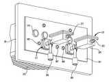
- the power feedthrough 321 shown in FIG. 3has a power lead 323 and a tensioner 325 .
- the power feedthrough 321provides both mechanical and electrical support for the wire and allows the wire to be placed in the path of the gas flow.
- the power feedthrough 321is connected to the gas distribution plate 30 through a mounting block 327 which may include an insulator to electrically isolate the power lead 323 and the wire from the gas distribution plate.
- the wire in the embodiment of FIG. 3extends through the first precursor gas channels and can be individual wires or a single wire which wraps around the second precursor gas channel.
- FIG. 6shows a detailed embodiment of the invention in which the gas distribution plate is in an ABA configuration and the wire 601 is a single wire extending along both first precursor gas ports (A and A′) and wrapping around the second precursor gas port B.
- An insulating material 603may be present at the end of the gas distribution plate 30 so that the wire 601 does not contact the gas distribution plate 30 .
- the portions of the wire 601 not exposed in the gas channelscan be insulated.
- the wire 601has been illustrated in an open channel 317 , meaning a channel without a plurality of openings (as shown in FIG. 4 ). However, the wire 601 could also be placed within the channel 317 behind the plurality of openings.
- the power leads 323(see FIG. 3 ) at the input face 301 must be of opposite polarity to allow current flow. Therefore, one power lead 323 will be positive and other negative.
- This configurationmay be relatively easy to setup, with a single power source being connected to both of the power leads 323 .
- the single power source(not shown) may include a mechanism to control the current flowing through the wire, such as a potentiometer.
- the gas distribution plateis made up of an ABA configuration and there are two wires.
- Each of the two wiresextend along one of the leading first precursor port A and the trailing first precursor gas port A′. Accordingly, each of the wires needs to have a separate power source for supplying a flow of current across the wire. Additionally, each wire will need a second power lead 324 for connection with the power supply to complete the circuit. In some embodiments, the wire extends along the second precursor gas port to excited species in the second precursor gas.
- the wire of some embodimentscan be part of a discrete hot wire unit.
- the hot wire unitcan be inserted into the gas distribution plate 30 through one of the gas inlets in the input face.
- the wire, associated clamps, power leads and tensionerare combined as a single unit.
- the unitcan have a tubular or rectangular cross-section and is sized to fit into the gas passageways within the gas distribution plate.
- the hot wire unitincludes an alternate gas inlet (as seen in FIG. 3 ), and openings to exhaust the gas flow. This allows the gas to flow through the hot wire unit, contacting the wire and being exhausted from the output face of the gas distribution plate.
- the gas distribution plate 30comprises a plurality if elongate gas ports consisting essentially of, in order, at least two repeating units of alternating first precursor gas A ports and second precursor gas B ports followed by a trailing first precursor gas A′ port. Stated differently, a combination of a first precursor gas A port and a second precursor gas B port, which may be referred to as an AB unit, is repeated at least two times, with a trailing first precursor gas A′ port.
- FIGS. 8 and 9illustrate embodiments of these sorts.
- the gas distribution plates 30 shown in FIGS. 8 and 9only show channels 317 associated with the first precursor gas A and the second precursor gas B.
- the purge gases and vacuum portshave been omitted for illustrative purposes only. Additionally, each of the channels 317 is illustrated as open channels without a plurality of openings as seen in FIG. 4 . Those skilled in the art will understand that the purge, vacuum and plurality of openings may be present in the gas distribution plate 30 .
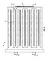
- FIG. 8has two repeating AB units with a trailing first precursor gas port A′, resulting in an ABABA configuration. Accordingly, each full cycle (one back and forth movement of a substrate through the gas streams) will result in deposition of four layers of B.
- FIG. 9is similar to that of FIG. 8 with the addition of a third AB unit. This makes a gas distribution plate with an ABABABA configuration. Accordingly, each full cycle will result in the deposition of six layers of B. Including a trailing first precursor gas port A′ in each of these configurations ensures that a substrate moving relative to the gas distribution plate will encounter a first precursor gas port before a second precursor gas port regardless of which side of the gas distribution plate 30 the movement originates.
- the embodiments showninclude two or three repeating AB units, it will be understood by those skilled in the art that there can be any number of repeating AB units in a given gas distribution plate 30 .
- the number of repeating AB unitscan vary depending on the size of the gas distribution plate. In some embodiments, there are in the range of about 2 and about 128 AB units. In various embodiments, there are at least about 2, 3, 4, 5, 10, 15, 20, 25, 30, 35, 40, 45 or 50 AB units. Additionally, it will be understood by those skilled in the art that this configuration is merely illustrative and that the gas distribution plate can comprise any number of gas injectors.
- a gas distribution platemay have 100 repeating AB units, with or without a trailing first gas port A′.
- the wire 601extends along each of the first precursor gas ports.
- the wirecan be a single wire which winds through the various first precursor gas ports.
- a second power lead 324is positioned at the end of the trailing first precursor gas A′ port.
- both terminals of the power leads 323are positioned on the same side of the gas distribution plate 30 .
- the wireis shown in the first precursor gas ports, it will be understood that the wire can extend along each of the second precursor gas ports, instead of, or in addition to a wire in the first precursor gas ports.
- individual wirescan be employed for each of the precursor gas ports, similar to FIG. 7 . When individual wires are used, there must be separate positive and negative power leads for each wire.
- FIG. 10shows another embodiment of the invention in which the wire 601 is mounted within an enclosure 1000 .
- the enclosure 1000can be sized to fit within the channels 317 of the gas distribution plate 30 so that the wire can 601 can be easily added or removed from the gas distribution plate 30 .
- the enclosure 1000can be attached to the output face of the gas distribution plate 30 and positioned so that the gases exiting the precursor gas port passes through the enclosure 1000 .
- the enclosuremay also include electrical leads 1010 in electrical communication with the wire 601 to allow current flow through the wire 601 .
- the electrical leads 1010can interact with electrical contacts positioned on the gas distribution plate. For example, pairs of electrical contacts (positive and negative contacts) can be included in the channels of the gas distribution plate. Each of these electrical contact pairs can be powered individually or as one or more units.
- the electrical leads 1010 on the enclosureform an electrical connection with the electrical contacts on the gas distribution plate so that current can flow through the wire 601 .
- Incorporating the wire 601 into the enclosures 1000allows the wire 601 to be easily removed from the processing chamber to be replaced or cleaned.
- the wire 601is maintained at a selected tension or in a range of tensions. Heating the wire will cause the wire to expand and sag.
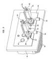
- a tensioner 325shown in an isometric cross-sectional view in FIG. 11 can be included.
- the tensioner 325is connected to the wire 601 to provide a tension on the wire 601 .
- a clamp 1110holds a first end of the wire 601 in connection with the power lead 323 (not shown touching).
- a bushing 1130connects the tensioner 325 with the gas port and may provide a gas tight seal so that precursor gases flowing into the gas port are not able to flow into the tensioner body.
- a spring 1120is positioned between the bushing 1130 and the clamp 1110 to provide the tension on the wire 601 . Although a spring 1120 is shown and described, it should be understood that other tensioning mechanisms can be employed.
- the tensioner 325is capable of providing sufficient tension to prevent significant sagging in the wire. Additionally, the tensioner 325 is configured to provide less tension on the wire than would be required to cause breakage of the wire.
- the term “significant sagging”means that there is a sag to length ratio of less than about 0.1, or less than about 0.05, or less than about 0.01, or less than about 0.005 or less than about 0.0025.
- the sagis less than about 4 mm over a 400 mm length, or less than about 3 mm over a 400 mm length, or less than about 2 mm over a 400 mm length, or less than about 1 mm over a 400 mm length, or less than about 4 mm over a 300 mm length, or less than about 3 mm over a 300 mm length, or less than about 2 mm over a 300 mm length, or less than about 1 mm over a 300 mm length.
- Springsmay be useful as tensioning mechanisms because the materials and spring constants can be tuned to match the requirements of the particular wire parameters (e.g., material, length, thickness).
- Additional embodiments of the inventionare directed to methods of processing a substrate.
- a substrateis laterally moved adjacent a gas distribution plate 30 as described herein.
- the substratecan be moved either beneath or above the gas distribution plate.
- a first precursor gasis delivered to the substrate surface from a first precursor gas port.
- a second precursor gasis delivered to the substrate surface from a second precursor gas port.
- a wireis positioned within one or more of the first precursor gas port and the second precursor gas port. Power is applied to the wire to cause the temperature of the wire to become elevated.
- the wireis elevated to a temperature high enough to cause excitation of gaseous species passing the wire.
- the excited speciesreact with the substrate surface.
- Another embodiment of the inventionis directed to a method of processing a substrate.
- the substrateis moved laterally adjacent a gas distribution plate.
- the gas distribution platehas a plurality of elongate gas ports consisting essentially of, in order, a leading first precursor gas port, a second precursor gas port and a trailing first precursor gas port.
- the surface of the substrateis sequentially contacted with, in order, a first precursor gas stream from the leading first precursor gas port, a second precursor gas stream from the second precursor gas port and a first precursor gas stream from the trailing first precursor gas port.
- Gaseous species, from either or both of the first precursor gas and the second precursor gasis excited by exposing the gas to high temperature wire within the path of the gas stream before the gas contacts the surface of the substrate.
- Embodiments of the inventioncan be incorporated into systems with a single gas distribution plate were met gas distribution plates.
- one or more embodimentsare used in a carousel type processing system in which one or more substrates are transported in a circular or oval path adjacent one or more gas distribution plates. This may be particularly useful for high throughput operations.
- Suitable apparatuses that can incorporate the gas distribution plates describedcan be any shape and are not limited to linear or round processing paths. Those skilled in the art will understand the matter in which these gas distribution plates can be employed.
Landscapes
- Chemical & Material Sciences (AREA)
- General Chemical & Material Sciences (AREA)
- Chemical Kinetics & Catalysis (AREA)
- Engineering & Computer Science (AREA)
- Materials Engineering (AREA)
- Mechanical Engineering (AREA)
- Metallurgy (AREA)
- Organic Chemistry (AREA)
- Chemical Vapour Deposition (AREA)
Abstract
Description
- This application claims the benefit under 35 U.S.C. 119(e) to U.S. Provisional Application No. 61/478,102, filed Apr. 22, 2011.
- Embodiments of the invention generally relate to an apparatus and a method for depositing materials. More specifically, embodiments of the invention are directed to a atomic layer deposition chambers with a hot wire for exciting gaseous species before contacting the substrate surface.
- In the field of semiconductor processing, flat-panel display processing or other electronic device processing, vapor deposition processes have played an important role in depositing materials on substrates. As the geometries of electronic devices continue to shrink and the density of devices continues to increase, the size and aspect ratio of the features are becoming more aggressive, e.g., feature sizes of 0.07 μm and aspect ratios of 10 or greater. Accordingly, conformal deposition of materials to form these devices is becoming increasingly important.
- During an atomic layer deposition (ALD) process, reactant gases are sequentially introduced into a process chamber containing a substrate. Generally, a first reactant is introduced into a process chamber and is adsorbed onto the substrate surface. A second reactant is then introduced into the process chamber and reacts with the first reactant to form a deposited material. A purge step may be carried out between the delivery of each reactant gas to ensure that the only reactions that occur are on the substrate surface. The purge step may be a continuous purge with a carrier gas or a pulse purge between the delivery of the reactant gases.
- There is an ongoing need in the art for apparatuses and methods of rapidly and efficiently processing substrates by atomic layer deposition.
- Embodiments of the invention are directed to gas distribution plates comprising an input face, an output face and a wire. The input face comprises a first precursor gas input configured to receive a flow of a first precursor gas and a second precursor gas input configured to receive a flow of a second precursor gas. The output face has a plurality of elongate gas ports configured to direct flows of gases toward a substrate adjacent the output face. The elongate gas ports include at least one first precursor gas port and at least one second precursor gas port. The at least one first precursor gas port is in flow communication with the first precursor gas and the at least one second precursor gas port in flow communication with the second precursor gas. The wire is positioned within at least one of the first precursor gas port and the second precursor gas port and is connected to a power source to heat the wire. In detailed embodiments, the wire comprises tungsten. In detailed embodiments, the wire can be heated to excite species in a gas flowing across the wire.
- In some embodiments, the gas distribution plate further comprises a tensioner connected to the wire to provide a tension. In detailed embodiments, the tensioner comprises a spring. In specific embodiments, the tension is sufficient to prevent significant sagging in the wire and breakage of the wire. According to some embodiments, the tensioner is attached to the input face of the gas distribution plate.
- According to some embodiments, the wire is within an enclosure attached to the output face and positioned so that gases exiting one or more of the first precursor gas port and the second precursor gas port pas through the enclosure.
- In some embodiments, the plurality of elongate gas ports consist essentially of, in order, a leading first precursor gas port, a second precursor gas port and a trailing first precursor gas port. In detailed embodiments, the wire is a single wire extending along both first precursor gas ports and wrapping around the second precursor gas port. In specific embodiments, there are two wires, a first wire extending along the leading first precursor gas port and a second wire extending along the trailing first precursor gas port. In one or more embodiments, the wire extends along the at least one second precursor gas port.
- In some embodiments, the plurality of elongate gas ports consist essentially of, in order, at least two repeating units of alternating first precursor gas ports and second precursor gas ports followed by a trailing first precursor gas port. In detailed embodiments, the wire extends along each of the first precursor gas ports. In specific embodiments, the wire extends along each of the second precursor gas ports.
- Additional embodiments of the invention are directed to processing chambers with the gas distribution plate described.
- Further embodiments of the invention are directed to methods of processing a substrate. A substrate having a surface is laterally moved beneath a gas distribution plate comprising a plurality of elongate gas ports including at least one first precursor gas port configured to deliver a first precursor gas and at least one second precursor gas port configured to deliver a second precursor gas. The first precursor is delivered to the substrate surface. The second precursor gas is delivered to the substrate surface. Power is applied to a wire positioned within one or more of the at least one first precursor gas port and the at least one second precursor gas port to excite gaseous species in one or more of the first precursor gas and the second precursor gas, the excited species reacting with the surface of the substrate. Detailed embodiments further comprise applying a tension to the wire, the tension sufficient to prevent significant sagging of the wire and breakage of the wire.
- Some embodiments of the invention are directed to methods of processing a substrate. A substrate is moved laterally adjacent a gas distribution plate having a plurality of elongate gas ports. The plurality of elongate gas ports consist essentially of, in order, a leading first precursor gas port, a second precursor gas port and a trailing first precursor gas port. A surface of the substrate is sequentially contacted with, in order, a first precursor gas stream from the leading first precursor gas port, a second precursor gas stream from the second precursor gas port and a first precursor gas stream from the trailing first precursor gas port. A gaseous species in one or more of the first precursor gas and the second precursor gas is excited before contacting the surface of the substrate by powering a wire positioned within either both the leading and trailing first precursor gas port or the second precursor gas port. In detailed embodiments, the method further comprises adjusting the tension of the wire to prevent substantial sagging and breakage of the wire.
- So that the manner in which the above recited features of the invention are attained and can be understood in detail, a more particular description of the invention, briefly summarized above, may be had by reference to the embodiments thereof which are illustrated in the appended drawings. It is to be noted, however, that the appended drawings illustrate only typical embodiments of this invention and are therefore not to be considered limiting of its scope, for the invention may admit to other equally effective embodiments.
FIG. 1 shows a schematic cross-sectional side view of an atomic layer deposition chamber according to one or more embodiments of the invention;FIG. 2 shows a perspective view of a susceptor in accordance with one or more embodiments of the invention;FIG. 3 shows a perspective view of a gas distribution plate in accordance with one or more embodiments of the invention;FIG. 4 shows a front view of a gas distribution plate in accordance with one or more embodiments of the invention;FIG. 5 shows a front view of a gas distribution plate in accordance with one or more embodiments of the invention;FIG. 6 shows a front view of a gas distribution plate in accordance with one or more embodiments of the invention;FIG. 7 shows a front view of a gas distribution plate in accordance with one or more embodiments of the invention;FIG. 8 shows a front view of a gas distribution plate in accordance with one or more embodiments of the invention;FIG. 9 shows a front view of a gas distribution plate in accordance with one or more embodiments of the invention;FIG. 10 shows a perspective view of a wire enclosure for use with gas distribution plates in accordance with one or more embodiments of the invention;FIG. 11 shows an isometric cross-section of a tensioner in accordance with one or more embodiments of the invention;FIG. 12 shows a cross-sectional view of a gas distribution plate in accordance with one or more embodiments of the invention;FIG. 13 shows a cross-sectional view of a gas distribution plate in accordance with one or more embodiments of the invention; andFIG. 14 Shows a front view of a channel of a gas distribution plate in accordance with one or more embodiments of the invention.- Embodiments of the invention are directed to atomic layer deposition apparatus and methods which provide excited gaseous species for reaction with the substrate surface. As used in this specification and the appended claims, the term “exited gaseous species” means any gaseous species not in the ground electronic state. For example, molecular oxygen may be excited to form oxygen radicals. The oxygen radicals being the excited species. Additionally, the terms “excited species”, “radical species” and the like are intended to mean a species not in the ground state. As used in this specification and the appended claims, the term “substrate surface” means the bare surface of the substrate or a layer (e.g., an oxide layer) on the bare substrate surface.
- Embodiments of the invention relate to the implementation of hot wire technology to spatial atomic layer deposition. In traditional applications, either globally elevated temperature or plasma (e.g., DC, RF, microwave) technologies were used. According to one or more embodiments, the implementation of hot wire technology creates a localized high temperature during an ALD process. With this hot wire technology in spatial ALD processes, one or more of the temperature, power and quantity of other gases required for the process can be reduced. This reduces the cost of processing substrates and is more reliable to manufacture the process chamber and achieve higher throughput and film quality.
- Generally, embodiments of the invention place a compatible material single wire or wires at a certain distance above the substrate. A certain tension is applied to the single wire or wires. Current flowing through the wire creates a localized high temperature which excites the reactant. When the radicalized species meet the precursor, they deposit a quality film on the substrate. The hot wire can be a single device such as a tubular device inserted from the front or a flange mount device mounted from the bottom. It contains all the necessary components to hold and tension the wire or wires, provide current to the wire or wires, component or material to compensate for the elongation of the wire and container, then place this single device at the path of reactant above the substrate. The wire can be integrally formed with the gas shower head together to simplify the power requirements. The wire can be formed in either a U shape, S shape or circular shape in the reactant path with one positive and one negative current lead for the whole shower head.
FIG. 1 is a schematic cross-sectional view of an atomiclayer deposition system 100 or reactor in accordance with one or more embodiments of the invention. Thesystem 100 includes a load lock chamber10 and aprocessing chamber 20. Theprocessing chamber 20 is generally a sealable enclosure, which is operated under vacuum, or at least low pressure. Theprocessing chamber 20 is isolated from the load lock chamber10 by an isolation valve15. The isolation valve15 seals theprocessing chamber 20 from the load lock chamber10 in a closed position and allows asubstrate 60 to be transferred from the load lock chamber10 through the valve to theprocessing chamber 20 and vice versa in an open position.- The
system 100 includes agas distribution plate 30 capable of distributing one or more gases across asubstrate 60. Thegas distribution plate 30 can be any suitable distribution plate known to those skilled in the art, and specific gas distribution plates described should not be taken as limiting the scope of the invention. The output face of thegas distribution plate 30 faces thefirst surface 61 of thesubstrate 60. - Substrates for use with the embodiments of the invention can be any suitable substrate. In detailed embodiments, the substrate is a rigid, discrete, generally planar substrate. As used in this specification and the appended claims, the term “discrete” when referring to a substrate means that the substrate has a fixed dimension. The substrate of specific embodiments is a semiconductor wafer, such as a 200 mm or 300 mm diameter silicon wafer.
- The
gas distribution plate 30 comprises a plurality of gas ports configured to transmit one or more gas streams to thesubstrate 60 and a plurality of vacuum ports disposed between each gas port and configured to transmit the gas streams out of theprocessing chamber 20. In the detailed embodiment ofFIG. 1 , thegas distribution plate 30 comprises afirst precursor injector 120, asecond precursor injector 130 and apurge gas injector 140. Theinjectors precursor injector 120 is configured to inject a continuous (or pulse) stream of a reactive precursor of compound A, a first precursor, into theprocessing chamber 20 through a plurality ofgas ports 125. Theprecursor injector 130 is configured to inject a continuous (or pulse) stream of a reactive precursor of compound B, a second precursor, into theprocessing chamber 20 through a plurality ofgas ports 135. Thepurge gas injector 140 is configured to inject a continuous (or pulse) stream of a non-reactive or purge gas into theprocessing chamber 20 through a plurality ofgas ports 145. The purge gas is configured to remove reactive material and reactive by-products from theprocessing chamber 20. The purge gas is typically an inert gas, such as, nitrogen, argon and helium.Gas ports 145 are disposed in betweengas ports 125 andgas ports 135 so as to separate the precursor of compound A from the precursor of compound B, thereby avoiding cross-contamination between the precursors. As used in this specification and the appended claims, the terms “reactive gas”, “reactive precursor”, “first precursor”, “second precursor” and the like, refer to gases and gaseous species capable of reacting with a substrate surface. - In another aspect, a remote plasma source (not shown) may be connected to the
precursor injector 120 and theprecursor injector 130 prior to injecting the precursors into thechamber 20. The plasma of reactive species may be generated by applying an electric field to a compound within the remote plasma source. Any power source that is capable of activating the intended compounds may be used. For example, power sources using DC, radio frequency (RF), and microwave (MW) based discharge techniques may be used. If an RF power source is used, it can be either capacitively or inductively coupled. The activation may also be generated by a thermally based technique, a gas breakdown technique, a high intensity light source (e.g., UV energy), or exposure to an x-ray source. Exemplary remote plasma sources are available from vendors such as MKS Instruments, Inc. and Advanced Energy Industries, Inc. The frequency of power used to generate the plasma can be any known and suitable frequency. For example, the plasma frequency can be 2 MHz, 13,56 MHz, 40 MHz or 60 MHz, but other frequencies may be beneficial as well. - The
system 100 further includes apumping system 150 connected to theprocessing chamber 20. Thepumping system 150 is generally configured to evacuate the gas streams out of theprocessing chamber 20 through one ormore vacuum ports 155. Thevacuum ports 155 are disposed between each gas port so as to evacuate the gas streams out of theprocessing chamber 20 after the gas streams react with the substrate surface and to further limit cross-contamination between the precursors. - The
system 100 includes a plurality ofpartitions 160 disposed on theprocessing chamber 20 between each port. A lower portion of each partition extends close to thefirst surface 61 ofsubstrate 60. For example, about 0.5 mm or greater from thefirst surface 61. In this manner, the lower portions of thepartitions 160 are separated from the substrate surface by a distance sufficient to allow the gas streams to flow around the lower portions toward thevacuum ports 155 after the gas streams react with the substrate surface.Arrows 198 indicate the direction of the gas streams. Since thepartitions 160 operate as a physical barrier to the gas streams, they also limit cross-contamination between the precursors. The arrangement shown is merely illustrative and should not be taken as limiting the scope of the invention. It will be understood by those skilled in the art that the gas distribution system shown is merely one possible distribution system and the other types of showerheads may be employed. - In operation, a
substrate 60 is delivered (e.g., by a robot) to the load lock chamber10 and is placed on ashuttle 65. After the isolation valve15 is opened, theshuttle 65 is moved along thetrack 70. Once thesubstrate 60 enters in theprocessing chamber 20, the isolation valve15 closes, sealing theprocessing chamber 20. Theshuttle 65 is then moved through theprocessing chamber 20 for processing. In one embodiment, theshuttle 65 is moved in a linear path through the chamber. - As the
substrate 60 moves through theprocessing chamber 20, thefirst surface 61 ofsubstrate 60 is repeatedly exposed to the precursor of compound A emitted fromgas ports 125 and the precursor of compound B emitted fromgas ports 135, with the purge gas emitted fromgas ports 145 in between. Injection of the purge gas is designed to remove unreacted material from the previous precursor prior to exposing thesubstrate surface 61 to the next precursor. After each exposure to the various gas streams (e.g., the precursors or the purge gas), the gas streams are evacuated through thevacuum ports 155 by thepumping system 150. Since a vacuum port may be disposed on both sides of each gas port, the gas streams are evacuated through thevacuum ports 155 on both sides. Thus, the gas streams flow from the respective gas ports vertically downward toward thefirst surface 61 of thesubstrate 60, across the substrate surface and around the lower portions of thepartitions 160, and finally upward toward thevacuum ports 155. In this manner, each gas may be uniformly distributed across thesubstrate surface 61.Arrows 198 indicate the direction of the gas flow.Substrate 60 may also be rotated while being exposed to the various gas streams. Rotation of the substrate may be useful in preventing the formation of strips in the formed layers. Rotation of the substrate can be continuous or in discreet steps. - The extent to which the
substrate surface 61 is exposed to each gas may be determined by, for example, the flow rates of each gas coming out of the gas port and the rate of movement of thesubstrate 60. In one embodiment, the flow rates of each gas are configured so as not to remove adsorbed precursors from thesubstrate surface 61. The width between each partition, the number of gas ports disposed on theprocessing chamber 20, and the number of times the substrate is passed back and forth may also determine the extent to which thesubstrate surface 61 is exposed to the various gases. Consequently, the quantity and quality of a deposited film may be optimized by varying the above-referenced factors. - In another embodiment, the
system 100 may include aprecursor injector 120 and aprecursor injector 130, without apurge gas injector 140. Consequently, as thesubstrate 60 moves through theprocessing chamber 20, thesubstrate surface 61 will be alternately exposed to the precursor of compound A and the precursor of compound B, without being exposed to purge gas in between. - The embodiment shown in
FIG. 1 has thegas distribution plate 30 above the substrate. While the embodiments have been described and shown with respect to this upright orientation, it will be understood that the inverted orientation is also possible. In that situation, thefirst surface 61 of thesubstrate 60 will face downward, while the gas flows toward the substrate will be directed upward. In one or more embodiments, at least one radiant heat source90 is positioned to heat the second side of the substrate. - The
gas distribution plate 30 can be of any suitable length, depending on the number of layers being deposited onto thesubstrate surface 61. Some embodiments of the gas distribution plate are intended to be used in a high throughput operation in which the substrate moves in one direction from a first end of the gas distribution plate to the second end of the gas distribution plate. During this single pass, a complete film is formed on the substrate surface based on the number of gas injectors in the gas distribution plate. In some embodiments, the gas distribution plate has more injectors than are needed to form a complete film. The individual injectors may be controlled so that some are inactive or only exhaust purge gases. For example, if the gas distribution plate has one hundred injectors for each of precursor A and precursor B, but only 50 are needed, then 50 injectors can be disabled. These disabled injectors can be grouped or dispersed throughout the gas distribution plate. - Additionally, although the drawings show a first precursor gas A and a second precursor gas B, it should be understood that the embodiments of the invention are not limited to gas distribution plates with only two different precursors. There can be, for examples, a third precursor C and fourth precursor D dispersed throughout the gas distribution plate. This would enable one to create films with mixed or stacked layers.
- In some embodiments, the
shuttle 65 is asusceptor 66 for carrying thesubstrate 60. Generally, thesusceptor 66 is a carrier which helps to form a uniform temperature across the substrate. Thesusceptor 66 is movable in both directions (left-to-right and right-to-left, relative to the arrangement ofFIG. 1 ) between the load lock chamber10 and theprocessing chamber 20. Thesusceptor 66 has atop surface 67 for carrying thesubstrate 60. Thesusceptor 66 may be a heated susceptor so that thesubstrate 60 may be heated for processing. As an example, thesusceptor 66 may be heated by radiant heat source90, a heating plate, resistive coils, or other heating devices, disposed underneath thesusceptor 66. - In still another embodiment, the
top surface 67 of thesusceptor 66 includes arecess 68 configured to accept thesubstrate 60, as shown inFIG. 2 . Thesusceptor 66 is generally thicker than the thickness of the substrate so that there is susceptor material beneath the substrate. In detailed embodiments, therecess 68 is configured such that when thesubstrate 60 is disposed inside therecess 68, thefirst surface 61 ofsubstrate 60 is level with thetop surface 67 of thesusceptor 66. Stated differently, therecess 68 of some embodiments is configured such that when asubstrate 60 is disposed therein, thefirst surface 61 of thesubstrate 60 does not protrude above thetop surface 67 of thesusceptor 66. FIGS. 3-9 showgas distribution plates 30 in accordance with various embodiments of the invention. Thegas distribution plates 30 comprise aninput face 301 and anoutput face 303. The input face301 (shown inFIG. 3 ) has a firstprecursor gas input 305 for receiving a flow of a first precursor gas A and a secondprecursor gas input 307 for receiving a flow of a second precursor gas B. Theinput face 301 also hasinputs 309 for one or more purge gases andports 311 for connecting to one or more vacuum ports. Although the configuration shown inFIG. 3 has two firstprecursor gas inputs 305, one secondprecursor gas input 307 and twopurge gas inputs 309 visible, it will be understood by those skilled in the art that there can be more or less of each of these components, individually or in combination.- The specific embodiments illustrated in
FIGS. 3-9 can be used with a reciprocal deposition system in which the substrate moves back and forth adjacent the gas distribution plate to deposit multiple layers. However, it should be understood that this is merely one embodiment and that the invention is not limited to reciprocal deposition techniques. Those skilled in the art will understand that a single large gas deposition plate with multiple sets of precursor injectors can be employed. - The
output face 303, shown inFIGS. 4-7 , has a plurality ofelongate gas ports 313. Thegas ports 313 are configured to direct flows of gases toward a substrate which may be positioned adjacent theoutput face 303. Theelongate gas ports 313 include at least one first precursor gas port and at least one second precursor gas port. Each first precursor gas port is in flow communication with the firstprecursor gas input 305 to allow the first precursor to flow through thegas distribution plate 30. Each second precursor gas port is in flow communication with the secondprecursor gas input 307 to allow the second precursor to flow through thegas distribution plate 30. - As shown in
FIG. 4 , the gas ports may include a plurality ofopenings 315 within achannel 317. Thechannel 317 is a recessed slot within the output face of the gas distribution plate. The gases flow out of theopenings 315 and are directed by thechannel 317 walls toward the substrate surface. Theopenings 315 are shown as being circular, but it should be understood that theopenings 315 can be any suitable shape including, but not limited to, square, rectangular and triangular. The number and size of theopenings 315 can also be changed to fit more or less openings within eachchannel 317. In the detailed embodiment shown inFIG. 4 , the purge gases (P), first precursor gas ports (A) and second precursor gas ports (B) comprise a plurality of openings positioned within channels. Theopenings 318 associated with the vacuum ports are on theoutput face 303 of thegas distribution plate 30, rather than in achannel 317, but could also be positioned within a channel. - The specific embodiment shown in
FIG. 4 has a combination of elongate gas ports that will provide a specific sequence of gas streams to a substrate surface when the substrate is moved perpendicularly to the elongate gas ports alongarrow 350. Although the substrate is described as being moved, it will be understood by those skilled in the art that the substrate can remain stationary and thegas distribution plate 30 can move. It is the relative movement between the substrate andgas distribution plate 30 that is referred to as substrate movement. The substrate, moving perpendicularly to the elongate gas ports will be subjected to gas flows of, in order, a purge gas stream, a first precursor gas A stream, a purge gas stream, a second precursor gas B stream, a purge gas stream, a first precursor gas A′ stream and a purge gas stream. Between each of the gas streams are vacuum ports which direct the gas streams out of the processing chamber. This results in a flow pattern in accordance witharrow 198 shown inFIG. 1 . - In specific embodiments, the gas distribution plate consists essentially of, in order, a leading first precursor gas port A, a second precursor gas port B and a trailing first precursor gas port A′. As used in this context, and in the appended claims, the term “consisting essentially of” means that the gas distribution plate does not include any additional gas ports for reactive gases. Ports for non-reactive gases (e.g, purge gases) and vacuum can be interspersed throughout while still being within the consisting essentially of clause. For example, the
gas distribution plate 30 may have eight vacuum ports V and four purge ports P but still consist essentially of a leading first precursor gas port A, a second precursor gas port B and a trailing precursor gas port A′. Embodiments of this variety may be referred to as an ABA configuration. - The use of the ABA configuration ensures that a substrate moving from either direction will encounter a first precursor gas A port before encountering a second precursor gas B port. Each pass across the
gas distribution plate 30 will result in a single film of composition B. Here, the two first precursor gas A ports surround the second precursor gas B port so that a substrate moving (relative to the gas distribution plate) from top-to-bottom of the figure will see, in order, the leading first reactive gas A, the second reactive gas B and the trailing first reactive gas A′, resulting in a full layer being formed on the substrate. A substrate returning along the same path will see the opposite order of reactive gases, resulting in two layers for each full cycle. A substrate moved back and forth across this gas distribution plate will be exposed to a pulse sequence of
AB AAB AAB (AAB)n. . . AABA- forming a uniform film composition of B. Exposure to the first precursor gas A at the end of the sequence is not important as there is no follow-up by a second precursor gas B. It will be understood by those skilled in the art that while the film composition is referred to as B, it is really a product of the surface reaction products of reactive gas A and reactive gas B and that use of just B is for convenience in describing the films.
FIG. 5 shows another detailed embodiment of thegas distribution plate 30 in which the channels for the leading first precursor gas port A and the trailing first precursor gas port A′ are fully open, as opposed to that ofFIG. 4 in which there are a plurality ofopenings 315 within thechannel 317. Again, this embodiment is shown in an ABA configuration but could just as easily include multiple sets of AB gas injectors spanning any desired number. For example, the gas distribution plate may have 100 sets of AB gas injectors, each individually controlled, and each individually containing a hot wire, tensioner and power source.- The
gas distribution plate 30, as shown inFIG. 6 , includes awire 601, which may be referred to as a hot wire, to excite gaseous species. Thewire 601 is positioned in either or both of the first precursor gas port and the second precursor gas port. The wire is connected to a power lead323 (shown inFIG. 3 ) configured to cause a flow of current through thewire 601 to heat thewire 601. Thewire 601 is heated to high temperatures to excite the species in the gas passing adjacent thewire 601. A purpose of the wire is to create the radical species in the gas, not to create a temperature increase in the substrate. The wire can be placed in a position in which there is no direct exposure to the surface of the substrate, while still be able to cause radical species formation in the gas. For example, if thewire 601 is placed in the second precursor gas ports, then the wire will cause a portion of the molecules in the second precursor gas to become excited. In the excited state the molecules have higher energy and are more likely to react with the substrate surface at a given processing temperature. - The placement of the wire may have an impact on the degree of radical species contacting the substrate. Placing the wire too far from the substrate may allow a larger number of radical species, than a closer placement, to become deactivated before contacting the substrate surface. The radical species may become deactivated by contact with other radicals, molecules in the gas stream and the gas distribution plate. However, placing the wire further from the substrate may help prevent the wire from heating the substrate surface while still creating radical species in the gas. The
wire 601 may be placed close enough to the surface of the substrate to ensure that excited species exist long enough to contact the surface without causing significant change in local temperature of the substrate. As used in this specification and the appended claims, the term “significant change in local temperature” means that the portion of the substrate adjacent the wire does not have an increase in temperature greater than about 10° C.FIG. 12 . Shows a side view of an embodiment of the invention in which thewire 601 is positioned withinchannel 317. This embodiment does not have a gas diffusing component (e.g., a showerhead or plurality of holes). With nothing to obstruct In some embodiments, theheated wire 601 may causes a change in temperature of a portion of the substrate adjacent the channel containing thewire 601.FIG. 13 shows another embodiment of the invention in which thewire 601 is positioned within achannel 317 having a gas diffusing component with a plurality ofopenings 315. Theheated wire 601 positioned behind the gas diffusing component may be capable of exciting the gaseous species without significantly changing the local temperature of the substrate. In detailed embodiments, the wire is heated to excite gaseous species while causing a surface temperature change of less than about 10° C. In various embodiments, the local change in temperature of the substrate surface is less than about 7° C., 5° C. or 3° C. In specific embodiments, the local temperature change is less than about 2° C., 1° C. or 0.5° C. - The wire can be made of any suitable material capable of being elevated to high temperature in a relatively short period of time. A suitable material is one which is compatible with the reactive gases. As used in this specification and the appended claims, the term “compatible” used in this regard means that the wire is not spontaneously reactive with the reactive gas at standard temperature and pressure. The temperature of the wire may have an impact on the degree of radicalization of the gaseous species. For example, oxygen may require temperature up to about 2000° C., while polymeric species may only need temperatures in the range of about 300° C. to about 500° C. In some embodiments, the wire is capable of being heated to a temperature of at least about 1000° C., 1100° C., 1200° C., 1300° C., 1400° C., 1500° C., 1600° C., 1700° C., 1800° C., 1900° C. or 2000° C. In various embodiments, the wire is capable of being heated to a temperature in the range of about 300° C. to about 2000° C., or in the range of about 700° C. and about 1400° C., or in the range of about 800° C. to about 1300° C. Power supplied to the wire can be modulated or turned on and off at any point throughout the processing. This allows the wire to be heated, creating excited gaseous species, for only a portion of the processing.
- The thickness and length of the wire can also be changed depending on the material used. Examples of suitable materials for the wire include, but are not limited to, tungsten, tantalum, iridium, ruthenium, nickel, chromium, graphite and alloys thereof. For example, where oxygen is the species being radicalized, the use of tantalum or tungsten may not be desired as these materials are sensitive to oxygen and may cause breakage of the wire. In detailed embodiments, the wire comprises tungsten.
- The wire can have any suitable density per unit length depending on the material used in the wire. In some embodiments, the wire has a substantially uniform density per unit length. As used in this specification and the appended claims, the term “substantially uniform” means that the density per unit length of the wire does not change by more than 20%, 15%, 10%, 5%, 3%, or 1% over the entire length of the wire. However, it may be advantageous to vary the density per unit length of the wire across the length of the wire. For example, upon heating the wire may tend to sag more in the middle of the length than at the end of the length. Here, a wire with a lower density per unit length in the middle of the wire may provide a more consistent process. However, in some embodiments, it may be more beneficial to have the middle of the wire length be of higher density per unit length.
- The shape of the wire can also be varied depending on factors such as, but not limited to, the degree of ionization desired and the material that the wire is made of. In some embodiments the wire is substantially straight or substantially linear. As used in this specification and the appended claims, the terms “substantially straight” and “substantially linear” mean that there is less than a 10%, 5%, 3% or 1% deviation in linearity of the wire over the entire length.
- In some embodiments, the wire has a nonlinear shape. For example, the liar can be folded, accordion shaped, looped or helical. We nonlinear wire is used, the tension provided on the ends of the wire may cause the wire shape to change slightly as the wire is heated up. Changing the shape of the wire may also provide a larger surface area upon which ionization can occur.
FIG. 14 shows a helical shaped wire in accordance with one or more embodiments of the invention. - Referring back to
FIG. 3 , the power source can be any suitable power source capable of controlling current flow through the wire. Thepower feedthrough 321 shown inFIG. 3 has apower lead 323 and atensioner 325. Thepower feedthrough 321 provides both mechanical and electrical support for the wire and allows the wire to be placed in the path of the gas flow. Thepower feedthrough 321 is connected to thegas distribution plate 30 through a mountingblock 327 which may include an insulator to electrically isolate thepower lead 323 and the wire from the gas distribution plate. The wire in the embodiment ofFIG. 3 extends through the first precursor gas channels and can be individual wires or a single wire which wraps around the second precursor gas channel. FIG. 6 shows a detailed embodiment of the invention in which the gas distribution plate is in an ABA configuration and thewire 601 is a single wire extending along both first precursor gas ports (A and A′) and wrapping around the second precursor gas port B.An insulating material 603 may be present at the end of thegas distribution plate 30 so that thewire 601 does not contact thegas distribution plate 30. Additionally, the portions of thewire 601 not exposed in the gas channels can be insulated. For ease of presentation, thewire 601 has been illustrated in anopen channel 317, meaning a channel without a plurality of openings (as shown inFIG. 4 ). However, thewire 601 could also be placed within thechannel 317 behind the plurality of openings.- In embodiments of the sort shown in
FIG. 6 , the power leads323 (seeFIG. 3 ) at theinput face 301 must be of opposite polarity to allow current flow. Therefore, onepower lead 323 will be positive and other negative. This configuration may be relatively easy to setup, with a single power source being connected to both of the power leads323. The single power source (not shown) may include a mechanism to control the current flowing through the wire, such as a potentiometer. - In an alternate detailed embodiment, shown in
FIG. 7 , the gas distribution plate is made up of an ABA configuration and there are two wires. Each of the two wires extend along one of the leading first precursor port A and the trailing first precursor gas port A′. Accordingly, each of the wires needs to have a separate power source for supplying a flow of current across the wire. Additionally, each wire will need asecond power lead 324 for connection with the power supply to complete the circuit. In some embodiments, the wire extends along the second precursor gas port to excited species in the second precursor gas. - The wire of some embodiments can be part of a discrete hot wire unit. The hot wire unit can be inserted into the
gas distribution plate 30 through one of the gas inlets in the input face. In these embodiments, the wire, associated clamps, power leads and tensioner are combined as a single unit. The unit can have a tubular or rectangular cross-section and is sized to fit into the gas passageways within the gas distribution plate. The hot wire unit includes an alternate gas inlet (as seen inFIG. 3 ), and openings to exhaust the gas flow. This allows the gas to flow through the hot wire unit, contacting the wire and being exhausted from the output face of the gas distribution plate. - In some embodiments, the
gas distribution plate 30 comprises a plurality if elongate gas ports consisting essentially of, in order, at least two repeating units of alternating first precursor gas A ports and second precursor gas B ports followed by a trailing first precursor gas A′ port. Stated differently, a combination of a first precursor gas A port and a second precursor gas B port, which may be referred to as an AB unit, is repeated at least two times, with a trailing first precursor gas A′ port.FIGS. 8 and 9 illustrate embodiments of these sorts. Thegas distribution plates 30 shown inFIGS. 8 and 9 only showchannels 317 associated with the first precursor gas A and the second precursor gas B. The purge gases and vacuum ports have been omitted for illustrative purposes only. Additionally, each of thechannels 317 is illustrated as open channels without a plurality of openings as seen inFIG. 4 . Those skilled in the art will understand that the purge, vacuum and plurality of openings may be present in thegas distribution plate 30. FIG. 8 has two repeating AB units with a trailing first precursor gas port A′, resulting in an ABABA configuration. Accordingly, each full cycle (one back and forth movement of a substrate through the gas streams) will result in deposition of four layers of B.FIG. 9 is similar to that ofFIG. 8 with the addition of a third AB unit. This makes a gas distribution plate with an ABABABA configuration. Accordingly, each full cycle will result in the deposition of six layers of B. Including a trailing first precursor gas port A′ in each of these configurations ensures that a substrate moving relative to the gas distribution plate will encounter a first precursor gas port before a second precursor gas port regardless of which side of thegas distribution plate 30 the movement originates. Although the embodiments shown include two or three repeating AB units, it will be understood by those skilled in the art that there can be any number of repeating AB units in a givengas distribution plate 30. The number of repeating AB units can vary depending on the size of the gas distribution plate. In some embodiments, there are in the range of about 2 and about 128 AB units. In various embodiments, there are at least about 2, 3, 4, 5, 10, 15, 20, 25, 30, 35, 40, 45 or 50 AB units. Additionally, it will be understood by those skilled in the art that this configuration is merely illustrative and that the gas distribution plate can comprise any number of gas injectors. For example, a gas distribution plate may have 100 repeating AB units, with or without a trailing first gas port A′.- In some embodiments, as shown in
FIGS. 8 and 9 , thewire 601 extends along each of the first precursor gas ports. The wire can be a single wire which winds through the various first precursor gas ports. InFIG. 8 , because there are an odd number of first precursor gas ports, asecond power lead 324 is positioned at the end of the trailing first precursor gas A′ port. InFIG. 9 , as there are an even number of first precursor gas ports, both terminals of the power leads323 are positioned on the same side of thegas distribution plate 30. Although the wire is shown in the first precursor gas ports, it will be understood that the wire can extend along each of the second precursor gas ports, instead of, or in addition to a wire in the first precursor gas ports. Additionally, individual wires can be employed for each of the precursor gas ports, similar toFIG. 7 . When individual wires are used, there must be separate positive and negative power leads for each wire. FIG. 10 shows another embodiment of the invention in which thewire 601 is mounted within anenclosure 1000. Theenclosure 1000 can be sized to fit within thechannels 317 of thegas distribution plate 30 so that the wire can601 can be easily added or removed from thegas distribution plate 30. Theenclosure 1000 can be attached to the output face of thegas distribution plate 30 and positioned so that the gases exiting the precursor gas port passes through theenclosure 1000. The enclosure may also includeelectrical leads 1010 in electrical communication with thewire 601 to allow current flow through thewire 601. The electrical leads1010 can interact with electrical contacts positioned on the gas distribution plate. For example, pairs of electrical contacts (positive and negative contacts) can be included in the channels of the gas distribution plate. Each of these electrical contact pairs can be powered individually or as one or more units. When anenclosure 1000 is inserted into thechannel 317 of the gas distribution plate, theelectrical leads 1010 on the enclosure form an electrical connection with the electrical contacts on the gas distribution plate so that current can flow through thewire 601. Incorporating thewire 601 into theenclosures 1000 allows thewire 601 to be easily removed from the processing chamber to be replaced or cleaned.- The
wire 601 is maintained at a selected tension or in a range of tensions. Heating the wire will cause the wire to expand and sag. To compensate for this sag, atensioner 325, shown in an isometric cross-sectional view inFIG. 11 can be included. Thetensioner 325 is connected to thewire 601 to provide a tension on thewire 601. Aclamp 1110 holds a first end of thewire 601 in connection with the power lead323 (not shown touching). Abushing 1130 connects thetensioner 325 with the gas port and may provide a gas tight seal so that precursor gases flowing into the gas port are not able to flow into the tensioner body. Aspring 1120 is positioned between thebushing 1130 and theclamp 1110 to provide the tension on thewire 601. Although aspring 1120 is shown and described, it should be understood that other tensioning mechanisms can be employed. - The
tensioner 325 is capable of providing sufficient tension to prevent significant sagging in the wire. Additionally, thetensioner 325 is configured to provide less tension on the wire than would be required to cause breakage of the wire. As used in this specification and the appended claims, the term “significant sagging” means that there is a sag to length ratio of less than about 0.1, or less than about 0.05, or less than about 0.01, or less than about 0.005 or less than about 0.0025. In various embodiments, the sag is less than about 4 mm over a 400 mm length, or less than about 3 mm over a 400 mm length, or less than about 2 mm over a 400 mm length, or less than about 1 mm over a 400 mm length, or less than about 4 mm over a 300 mm length, or less than about 3 mm over a 300 mm length, or less than about 2 mm over a 300 mm length, or less than about 1 mm over a 300 mm length. Springs may be useful as tensioning mechanisms because the materials and spring constants can be tuned to match the requirements of the particular wire parameters (e.g., material, length, thickness). - Additional embodiments of the invention are directed to methods of processing a substrate. A substrate is laterally moved adjacent a
gas distribution plate 30 as described herein. The substrate can be moved either beneath or above the gas distribution plate. A first precursor gas is delivered to the substrate surface from a first precursor gas port. A second precursor gas is delivered to the substrate surface from a second precursor gas port. A wire is positioned within one or more of the first precursor gas port and the second precursor gas port. Power is applied to the wire to cause the temperature of the wire to become elevated. The wire is elevated to a temperature high enough to cause excitation of gaseous species passing the wire. The excited species react with the substrate surface. - Another embodiment of the invention is directed to a method of processing a substrate. The substrate is moved laterally adjacent a gas distribution plate. The gas distribution plate has a plurality of elongate gas ports consisting essentially of, in order, a leading first precursor gas port, a second precursor gas port and a trailing first precursor gas port. The surface of the substrate is sequentially contacted with, in order, a first precursor gas stream from the leading first precursor gas port, a second precursor gas stream from the second precursor gas port and a first precursor gas stream from the trailing first precursor gas port. Gaseous species, from either or both of the first precursor gas and the second precursor gas is excited by exposing the gas to high temperature wire within the path of the gas stream before the gas contacts the surface of the substrate.
- Embodiments of the invention can be incorporated into systems with a single gas distribution plate were met gas distribution plates. For example, one or more embodiments are used in a carousel type processing system in which one or more substrates are transported in a circular or oval path adjacent one or more gas distribution plates. This may be particularly useful for high throughput operations. Suitable apparatuses that can incorporate the gas distribution plates described can be any shape and are not limited to linear or round processing paths. Those skilled in the art will understand the matter in which these gas distribution plates can be employed.
- Although the invention herein has been described with reference to particular embodiments, it is to be understood that these embodiments are merely illustrative of the principles and applications of the present invention. It will be apparent to those skilled in the art that various modifications and variations can be made to the method and apparatus of the present invention without departing from the spirit and scope of the invention. Thus, it is intended that the present invention include modifications and variations that are within the scope of the appended claims and their equivalents.
Claims (20)
1. A gas distribution plate, comprising:
an input face comprising a first precursor gas input configured to receive a flow of a first precursor gas and a second precursor gas input configured to receive a flow of a second precursor gas;
an output face having a plurality of elongate gas ports configured to direct flows of gases toward a substrate adjacent the output face, the elongate gas ports including at least one first precursor gas port and at least one second precursor gas port, the at least one first precursor gas port in flow communication with the first precursor gas and the at least one second precursor gas port in flow communication with the second precursor gas; and
a wire positioned within at least one of the first precursor gas port and the second precursor gas port, the wire connected to a power source to heat the wire.
2. The gas distribution plate ofclaim 1 , further comprising a tensioner connected to the wire to provide a tension.
3. The gas distribution plate ofclaim 2 , wherein the tensioner comprises a spring.
4. The gas distribution plate ofclaim 2 , wherein the tension is sufficient to prevent significant sagging in the wire and breakage of the wire.
5. The gas distribution plate ofclaim 2 , wherein the tensioner is attached to the input face.
6. The gas distribution plate ofclaim 1 , wherein the wire comprises tungsten.
7. The gas distribution plate ofclaim 1 , wherein the wire is within an enclosure attached to the output face and positioned so that gases exiting one or more of the first precursor gas port and the second precursor gas port pas through the enclosure.
8. The gas distribution plate ofclaim 1 , wherein the plurality of elongate gas ports consist essentially of, in order, a leading first precursor gas port, a second precursor gas port and a trailing first precursor gas port.
9. The gas distribution plate ofclaim 8 , wherein the wire is a single wire extending along both first precursor gas ports and wrapping around the second precursor gas port.
10. The gas distribution plate ofclaim 8 , wherein there are two wires, a first wire extending along the leading first precursor gas port and a second wire extending along the trailing first precursor gas port.
11. The gas distribution plate ofclaim 1 , wherein the wire extends along the at least one second precursor gas port.
12. The gas distribution plate ofclaim 1 , wherein the plurality of elongate gas ports consist essentially of, in order, at least two repeating units of alternating first precursor gas ports and second precursor gas ports followed by a trailing first precursor gas port.
13. The gas distribution plate ofclaim 12 , wherein the wire extends along each of the first precursor gas ports.
14. The gas distribution plate ofclaim 12 , wherein the wire extends along each of the second precursor gas ports.
15. The gas distribution plate ofclaim 1 , wherein the wire can be heated to excite species in a gas flowing across the wire.
16. A deposition system, comprising a processing chamber with the gas distribution plate ofclaim 1 .
17. A method of processing a substrate comprising:
laterally moving a substrate having a surface beneath a gas distribution plate comprising a plurality of elongate gas ports including at least one first precursor gas port to deliver a first precursor gas and at least one second precursor gas port to deliver a second precursor gas;
delivering the first precursor gas to the substrate surface;
delivering the second precursor gas to the substrate surface; and
applying power to a wire positioned within one or more of the at least one first precursor gas port and the at least one second precursor gas port to excite gaseous species in one or more of the first precursor gas and the second precursor gas, the excited species reacting with the surface of the substrate.
18. The method ofclaim 17 , further comprising applying a tension to the wire, the tension sufficient to prevent significant sagging of the wire and breakage of the wire.
19. A method of processing a substrate, comprising:
laterally moving the substrate adjacent a gas distribution plate having a plurality of elongate gas ports, the plurality of elongate gas ports consisting essentially of, in order, a leading first precursor gas port, a second precursor gas port and a trailing first precursor gas port;
sequentially contacting a surface of the substrate to, in order, a first precursor gas stream from the leading first precursor gas port, a second precursor gas stream from the second precursor gas port and a first precursor gas stream from the trailing first precursor gas port; and
exciting a gaseous species in one or more of the first precursor gas and the second precursor gas before contacting the surface of the substrate by powering a wire positioned within either both the leading and trailing first precursor gas port or the second precursor gas port.
20. The method ofclaim 19 , further comprising adjusting tension of the wire to prevent substantial sagging and breakage of the wire.
Priority Applications (6)
| Application Number | Priority Date | Filing Date | Title |
|---|---|---|---|
| US13/437,567US20120269967A1 (en) | 2011-04-22 | 2012-04-02 | Hot Wire Atomic Layer Deposition Apparatus And Methods Of Use |
| PCT/US2012/033029WO2012145205A2 (en) | 2011-04-22 | 2012-04-11 | Hot wire atomic layer deposition apparatus and methods of use |
| JP2014506453AJP2014515790A (en) | 2011-04-22 | 2012-04-11 | Hot wire atomic layer deposition apparatus and method of use |
| KR1020137030931AKR20140031906A (en) | 2011-04-22 | 2012-04-11 | Hot wire atomic layer deposition apparatus and methods of use |
| CN201280019433.0ACN103493179A (en) | 2011-04-22 | 2012-04-11 | Hot wire atomic layer deposition apparatus and methods of use |
| TW101113040ATW201243088A (en) | 2011-04-22 | 2012-04-12 | Hot wire atomic layer deposition apparatus and methods of use |
Applications Claiming Priority (2)
| Application Number | Priority Date | Filing Date | Title |
|---|---|---|---|
| US201161478102P | 2011-04-22 | 2011-04-22 | |
| US13/437,567US20120269967A1 (en) | 2011-04-22 | 2012-04-02 | Hot Wire Atomic Layer Deposition Apparatus And Methods Of Use |
Publications (1)
| Publication Number | Publication Date |
|---|---|
| US20120269967A1true US20120269967A1 (en) | 2012-10-25 |
Family
ID=47021538
Family Applications (1)
| Application Number | Title | Priority Date | Filing Date |
|---|---|---|---|
| US13/437,567AbandonedUS20120269967A1 (en) | 2011-04-22 | 2012-04-02 | Hot Wire Atomic Layer Deposition Apparatus And Methods Of Use |
Country Status (6)
| Country | Link |
|---|---|
| US (1) | US20120269967A1 (en) |
| JP (1) | JP2014515790A (en) |
| KR (1) | KR20140031906A (en) |
| CN (1) | CN103493179A (en) |
| TW (1) | TW201243088A (en) |
| WO (1) | WO2012145205A2 (en) |
Cited By (279)
| Publication number | Priority date | Publication date | Assignee | Title |
|---|---|---|---|---|
| US20110168094A1 (en)* | 2010-01-13 | 2011-07-14 | Honda Motor Co., Ltd. | Plasma film forming apparatus |
| US20160027674A1 (en)* | 2013-03-15 | 2016-01-28 | Kevin Griffin | Carousel Gas Distribution Assembly With Optical Measurements |
| US20170058402A1 (en)* | 2015-08-28 | 2017-03-02 | Samsung Electronics Co., Ltd. | Shower head of combinatorial spatial atomic layer deposition apparatus |
| FR3046800A1 (en)* | 2016-01-18 | 2017-07-21 | Enhelios Nanotech | METHOD AND DEVICE FOR CHEMICAL DEPOSITION IN GAS PHASE WITH ALTERNATE FLUX. |
| US20180277400A1 (en)* | 2017-03-23 | 2018-09-27 | Toshiba Memory Corporation | Semiconductor manufacturing apparatus |
| US10269593B2 (en)* | 2013-03-14 | 2019-04-23 | Applied Materials, Inc. | Apparatus for coupling a hot wire source to a process chamber |
| US11004977B2 (en) | 2017-07-19 | 2021-05-11 | Asm Ip Holding B.V. | Method for depositing a group IV semiconductor and related semiconductor device structures |
| US11001925B2 (en) | 2016-12-19 | 2021-05-11 | Asm Ip Holding B.V. | Substrate processing apparatus |
| US11018002B2 (en) | 2017-07-19 | 2021-05-25 | Asm Ip Holding B.V. | Method for selectively depositing a Group IV semiconductor and related semiconductor device structures |
| US11015245B2 (en) | 2014-03-19 | 2021-05-25 | Asm Ip Holding B.V. | Gas-phase reactor and system having exhaust plenum and components thereof |
| US11022879B2 (en) | 2017-11-24 | 2021-06-01 | Asm Ip Holding B.V. | Method of forming an enhanced unexposed photoresist layer |
| US11031242B2 (en) | 2018-11-07 | 2021-06-08 | Asm Ip Holding B.V. | Methods for depositing a boron doped silicon germanium film |
| USD922229S1 (en) | 2019-06-05 | 2021-06-15 | Asm Ip Holding B.V. | Device for controlling a temperature of a gas supply unit |
| US11049751B2 (en) | 2018-09-14 | 2021-06-29 | Asm Ip Holding B.V. | Cassette supply system to store and handle cassettes and processing apparatus equipped therewith |
| US11056344B2 (en) | 2017-08-30 | 2021-07-06 | Asm Ip Holding B.V. | Layer forming method |
| US11053591B2 (en) | 2018-08-06 | 2021-07-06 | Asm Ip Holding B.V. | Multi-port gas injection system and reactor system including same |
| US11069510B2 (en) | 2017-08-30 | 2021-07-20 | Asm Ip Holding B.V. | Substrate processing apparatus |
| US11081345B2 (en) | 2018-02-06 | 2021-08-03 | Asm Ip Holding B.V. | Method of post-deposition treatment for silicon oxide film |
| US11088002B2 (en) | 2018-03-29 | 2021-08-10 | Asm Ip Holding B.V. | Substrate rack and a substrate processing system and method |
| US11087997B2 (en) | 2018-10-31 | 2021-08-10 | Asm Ip Holding B.V. | Substrate processing apparatus for processing substrates |
| US11094582B2 (en) | 2016-07-08 | 2021-08-17 | Asm Ip Holding B.V. | Selective deposition method to form air gaps |
| US11094546B2 (en) | 2017-10-05 | 2021-08-17 | Asm Ip Holding B.V. | Method for selectively depositing a metallic film on a substrate |
| US11101370B2 (en) | 2016-05-02 | 2021-08-24 | Asm Ip Holding B.V. | Method of forming a germanium oxynitride film |
| US11107676B2 (en) | 2016-07-28 | 2021-08-31 | Asm Ip Holding B.V. | Method and apparatus for filling a gap |
| US11114294B2 (en) | 2019-03-08 | 2021-09-07 | Asm Ip Holding B.V. | Structure including SiOC layer and method of forming same |
| US11114283B2 (en) | 2018-03-16 | 2021-09-07 | Asm Ip Holding B.V. | Reactor, system including the reactor, and methods of manufacturing and using same |
| USD930782S1 (en) | 2019-08-22 | 2021-09-14 | Asm Ip Holding B.V. | Gas distributor |
| US11127589B2 (en) | 2019-02-01 | 2021-09-21 | Asm Ip Holding B.V. | Method of topology-selective film formation of silicon oxide |
| US11127617B2 (en) | 2017-11-27 | 2021-09-21 | Asm Ip Holding B.V. | Storage device for storing wafer cassettes for use with a batch furnace |
| USD931978S1 (en) | 2019-06-27 | 2021-09-28 | Asm Ip Holding B.V. | Showerhead vacuum transport |
| US11139308B2 (en) | 2015-12-29 | 2021-10-05 | Asm Ip Holding B.V. | Atomic layer deposition of III-V compounds to form V-NAND devices |
| US11139191B2 (en) | 2017-08-09 | 2021-10-05 | Asm Ip Holding B.V. | Storage apparatus for storing cassettes for substrates and processing apparatus equipped therewith |
| US11158513B2 (en) | 2018-12-13 | 2021-10-26 | Asm Ip Holding B.V. | Methods for forming a rhenium-containing film on a substrate by a cyclical deposition process and related semiconductor device structures |
| US11164955B2 (en) | 2017-07-18 | 2021-11-02 | Asm Ip Holding B.V. | Methods for forming a semiconductor device structure and related semiconductor device structures |
| USD935572S1 (en) | 2019-05-24 | 2021-11-09 | Asm Ip Holding B.V. | Gas channel plate |
| US11171025B2 (en) | 2019-01-22 | 2021-11-09 | Asm Ip Holding B.V. | Substrate processing device |
| US11168395B2 (en) | 2018-06-29 | 2021-11-09 | Asm Ip Holding B.V. | Temperature-controlled flange and reactor system including same |
| US11205585B2 (en) | 2016-07-28 | 2021-12-21 | Asm Ip Holding B.V. | Substrate processing apparatus and method of operating the same |
| US11217444B2 (en) | 2018-11-30 | 2022-01-04 | Asm Ip Holding B.V. | Method for forming an ultraviolet radiation responsive metal oxide-containing film |
| US11222772B2 (en) | 2016-12-14 | 2022-01-11 | Asm Ip Holding B.V. | Substrate processing apparatus |
| USD940837S1 (en) | 2019-08-22 | 2022-01-11 | Asm Ip Holding B.V. | Electrode |
| US11227782B2 (en) | 2019-07-31 | 2022-01-18 | Asm Ip Holding B.V. | Vertical batch furnace assembly |
| US11227789B2 (en) | 2019-02-20 | 2022-01-18 | Asm Ip Holding B.V. | Method and apparatus for filling a recess formed within a substrate surface |
| US11232963B2 (en) | 2018-10-03 | 2022-01-25 | Asm Ip Holding B.V. | Substrate processing apparatus and method |
| US11233133B2 (en) | 2015-10-21 | 2022-01-25 | Asm Ip Holding B.V. | NbMC layers |
| US11230766B2 (en) | 2018-03-29 | 2022-01-25 | Asm Ip Holding B.V. | Substrate processing apparatus and method |
| US11244825B2 (en) | 2018-11-16 | 2022-02-08 | Asm Ip Holding B.V. | Methods for depositing a transition metal chalcogenide film on a substrate by a cyclical deposition process |
| US11242598B2 (en) | 2015-06-26 | 2022-02-08 | Asm Ip Holding B.V. | Structures including metal carbide material, devices including the structures, and methods of forming same |
| US11251035B2 (en) | 2016-12-22 | 2022-02-15 | Asm Ip Holding B.V. | Method of forming a structure on a substrate |
| US11251068B2 (en) | 2018-10-19 | 2022-02-15 | Asm Ip Holding B.V. | Substrate processing apparatus and substrate processing method |
| US11251040B2 (en) | 2019-02-20 | 2022-02-15 | Asm Ip Holding B.V. | Cyclical deposition method including treatment step and apparatus for same |
| USD944946S1 (en) | 2019-06-14 | 2022-03-01 | Asm Ip Holding B.V. | Shower plate |
| US11270899B2 (en) | 2018-06-04 | 2022-03-08 | Asm Ip Holding B.V. | Wafer handling chamber with moisture reduction |
| US11274369B2 (en) | 2018-09-11 | 2022-03-15 | Asm Ip Holding B.V. | Thin film deposition method |
| US11282698B2 (en) | 2019-07-19 | 2022-03-22 | Asm Ip Holding B.V. | Method of forming topology-controlled amorphous carbon polymer film |
| US11289326B2 (en) | 2019-05-07 | 2022-03-29 | Asm Ip Holding B.V. | Method for reforming amorphous carbon polymer film |
| US11286558B2 (en) | 2019-08-23 | 2022-03-29 | Asm Ip Holding B.V. | Methods for depositing a molybdenum nitride film on a surface of a substrate by a cyclical deposition process and related semiconductor device structures including a molybdenum nitride film |
| US11286562B2 (en) | 2018-06-08 | 2022-03-29 | Asm Ip Holding B.V. | Gas-phase chemical reactor and method of using same |
| USD947913S1 (en) | 2019-05-17 | 2022-04-05 | Asm Ip Holding B.V. | Susceptor shaft |
| US11295980B2 (en) | 2017-08-30 | 2022-04-05 | Asm Ip Holding B.V. | Methods for depositing a molybdenum metal film over a dielectric surface of a substrate by a cyclical deposition process and related semiconductor device structures |
| US11296189B2 (en) | 2018-06-21 | 2022-04-05 | Asm Ip Holding B.V. | Method for depositing a phosphorus doped silicon arsenide film and related semiconductor device structures |
| USD948463S1 (en) | 2018-10-24 | 2022-04-12 | Asm Ip Holding B.V. | Susceptor for semiconductor substrate supporting apparatus |
| US11306395B2 (en) | 2017-06-28 | 2022-04-19 | Asm Ip Holding B.V. | Methods for depositing a transition metal nitride film on a substrate by atomic layer deposition and related deposition apparatus |
| USD949319S1 (en) | 2019-08-22 | 2022-04-19 | Asm Ip Holding B.V. | Exhaust duct |
| US11315794B2 (en) | 2019-10-21 | 2022-04-26 | Asm Ip Holding B.V. | Apparatus and methods for selectively etching films |
| US11342216B2 (en) | 2019-02-20 | 2022-05-24 | Asm Ip Holding B.V. | Cyclical deposition method and apparatus for filling a recess formed within a substrate surface |
| US11339476B2 (en) | 2019-10-08 | 2022-05-24 | Asm Ip Holding B.V. | Substrate processing device having connection plates, substrate processing method |
| US11345999B2 (en) | 2019-06-06 | 2022-05-31 | Asm Ip Holding B.V. | Method of using a gas-phase reactor system including analyzing exhausted gas |
| US11355338B2 (en) | 2019-05-10 | 2022-06-07 | Asm Ip Holding B.V. | Method of depositing material onto a surface and structure formed according to the method |
| US11361990B2 (en) | 2018-05-28 | 2022-06-14 | Asm Ip Holding B.V. | Substrate processing method and device manufactured by using the same |
| US11374112B2 (en) | 2017-07-19 | 2022-06-28 | Asm Ip Holding B.V. | Method for depositing a group IV semiconductor and related semiconductor device structures |
| US11378337B2 (en) | 2019-03-28 | 2022-07-05 | Asm Ip Holding B.V. | Door opener and substrate processing apparatus provided therewith |
| US11387120B2 (en) | 2017-09-28 | 2022-07-12 | Asm Ip Holding B.V. | Chemical dispensing apparatus and methods for dispensing a chemical to a reaction chamber |
| US11387106B2 (en) | 2018-02-14 | 2022-07-12 | Asm Ip Holding B.V. | Method for depositing a ruthenium-containing film on a substrate by a cyclical deposition process |
| US11393690B2 (en) | 2018-01-19 | 2022-07-19 | Asm Ip Holding B.V. | Deposition method |
| US11390950B2 (en) | 2017-01-10 | 2022-07-19 | Asm Ip Holding B.V. | Reactor system and method to reduce residue buildup during a film deposition process |
| US11390946B2 (en) | 2019-01-17 | 2022-07-19 | Asm Ip Holding B.V. | Methods of forming a transition metal containing film on a substrate by a cyclical deposition process |
| US11390945B2 (en) | 2019-07-03 | 2022-07-19 | Asm Ip Holding B.V. | Temperature control assembly for substrate processing apparatus and method of using same |
| US11396702B2 (en) | 2016-11-15 | 2022-07-26 | Asm Ip Holding B.V. | Gas supply unit and substrate processing apparatus including the gas supply unit |
| US11398382B2 (en) | 2018-03-27 | 2022-07-26 | Asm Ip Holding B.V. | Method of forming an electrode on a substrate and a semiconductor device structure including an electrode |
| US11401605B2 (en) | 2019-11-26 | 2022-08-02 | Asm Ip Holding B.V. | Substrate processing apparatus |
| US11410851B2 (en) | 2017-02-15 | 2022-08-09 | Asm Ip Holding B.V. | Methods for forming a metallic film on a substrate by cyclical deposition and related semiconductor device structures |
| US11414760B2 (en) | 2018-10-08 | 2022-08-16 | Asm Ip Holding B.V. | Substrate support unit, thin film deposition apparatus including the same, and substrate processing apparatus including the same |
| US11417545B2 (en) | 2017-08-08 | 2022-08-16 | Asm Ip Holding B.V. | Radiation shield |
| US11424119B2 (en) | 2019-03-08 | 2022-08-23 | Asm Ip Holding B.V. | Method for selective deposition of silicon nitride layer and structure including selectively-deposited silicon nitride layer |
| US11430674B2 (en) | 2018-08-22 | 2022-08-30 | Asm Ip Holding B.V. | Sensor array, apparatus for dispensing a vapor phase reactant to a reaction chamber and related methods |
| US11430640B2 (en) | 2019-07-30 | 2022-08-30 | Asm Ip Holding B.V. | Substrate processing apparatus |
| US11437241B2 (en) | 2020-04-08 | 2022-09-06 | Asm Ip Holding B.V. | Apparatus and methods for selectively etching silicon oxide films |
| US11443926B2 (en) | 2019-07-30 | 2022-09-13 | Asm Ip Holding B.V. | Substrate processing apparatus |
| US11447864B2 (en) | 2019-04-19 | 2022-09-20 | Asm Ip Holding B.V. | Layer forming method and apparatus |
| US11447861B2 (en) | 2016-12-15 | 2022-09-20 | Asm Ip Holding B.V. | Sequential infiltration synthesis apparatus and a method of forming a patterned structure |
| US11453943B2 (en) | 2016-05-25 | 2022-09-27 | Asm Ip Holding B.V. | Method for forming carbon-containing silicon/metal oxide or nitride film by ALD using silicon precursor and hydrocarbon precursor |
| USD965044S1 (en) | 2019-08-19 | 2022-09-27 | Asm Ip Holding B.V. | Susceptor shaft |
| USD965524S1 (en) | 2019-08-19 | 2022-10-04 | Asm Ip Holding B.V. | Susceptor support |
| US11469098B2 (en) | 2018-05-08 | 2022-10-11 | Asm Ip Holding B.V. | Methods for depositing an oxide film on a substrate by a cyclical deposition process and related device structures |
| US11476109B2 (en) | 2019-06-11 | 2022-10-18 | Asm Ip Holding B.V. | Method of forming an electronic structure using reforming gas, system for performing the method, and structure formed using the method |
| US11473195B2 (en) | 2018-03-01 | 2022-10-18 | Asm Ip Holding B.V. | Semiconductor processing apparatus and a method for processing a substrate |
| US11482533B2 (en) | 2019-02-20 | 2022-10-25 | Asm Ip Holding B.V. | Apparatus and methods for plug fill deposition in 3-D NAND applications |
| US11482412B2 (en) | 2018-01-19 | 2022-10-25 | Asm Ip Holding B.V. | Method for depositing a gap-fill layer by plasma-assisted deposition |
| US11482418B2 (en) | 2018-02-20 | 2022-10-25 | Asm Ip Holding B.V. | Substrate processing method and apparatus |
| US11488854B2 (en) | 2020-03-11 | 2022-11-01 | Asm Ip Holding B.V. | Substrate handling device with adjustable joints |
| US11488819B2 (en) | 2018-12-04 | 2022-11-01 | Asm Ip Holding B.V. | Method of cleaning substrate processing apparatus |
| US11495459B2 (en) | 2019-09-04 | 2022-11-08 | Asm Ip Holding B.V. | Methods for selective deposition using a sacrificial capping layer |
| US11492703B2 (en) | 2018-06-27 | 2022-11-08 | Asm Ip Holding B.V. | Cyclic deposition methods for forming metal-containing material and films and structures including the metal-containing material |
| US11499226B2 (en) | 2018-11-02 | 2022-11-15 | Asm Ip Holding B.V. | Substrate supporting unit and a substrate processing device including the same |
| US11501956B2 (en) | 2012-10-12 | 2022-11-15 | Asm Ip Holding B.V. | Semiconductor reaction chamber showerhead |
| US11501973B2 (en) | 2018-01-16 | 2022-11-15 | Asm Ip Holding B.V. | Method for depositing a material film on a substrate within a reaction chamber by a cyclical deposition process and related device structures |
| US11499222B2 (en) | 2018-06-27 | 2022-11-15 | Asm Ip Holding B.V. | Cyclic deposition methods for forming metal-containing material and films and structures including the metal-containing material |
| US11501968B2 (en) | 2019-11-15 | 2022-11-15 | Asm Ip Holding B.V. | Method for providing a semiconductor device with silicon filled gaps |
| US11515188B2 (en) | 2019-05-16 | 2022-11-29 | Asm Ip Holding B.V. | Wafer boat handling device, vertical batch furnace and method |
| US11515187B2 (en) | 2020-05-01 | 2022-11-29 | Asm Ip Holding B.V. | Fast FOUP swapping with a FOUP handler |
| US11521851B2 (en) | 2020-02-03 | 2022-12-06 | Asm Ip Holding B.V. | Method of forming structures including a vanadium or indium layer |
| US11527400B2 (en) | 2019-08-23 | 2022-12-13 | Asm Ip Holding B.V. | Method for depositing silicon oxide film having improved quality by peald using bis(diethylamino)silane |
| US11527403B2 (en) | 2019-12-19 | 2022-12-13 | Asm Ip Holding B.V. | Methods for filling a gap feature on a substrate surface and related semiconductor structures |
| US11530876B2 (en) | 2020-04-24 | 2022-12-20 | Asm Ip Holding B.V. | Vertical batch furnace assembly comprising a cooling gas supply |
| US11530483B2 (en) | 2018-06-21 | 2022-12-20 | Asm Ip Holding B.V. | Substrate processing system |
| US11532757B2 (en) | 2016-10-27 | 2022-12-20 | Asm Ip Holding B.V. | Deposition of charge trapping layers |
| US11551925B2 (en) | 2019-04-01 | 2023-01-10 | Asm Ip Holding B.V. | Method for manufacturing a semiconductor device |
| US11551912B2 (en) | 2020-01-20 | 2023-01-10 | Asm Ip Holding B.V. | Method of forming thin film and method of modifying surface of thin film |
| USD975665S1 (en) | 2019-05-17 | 2023-01-17 | Asm Ip Holding B.V. | Susceptor shaft |
| US11557474B2 (en) | 2019-07-29 | 2023-01-17 | Asm Ip Holding B.V. | Methods for selective deposition utilizing n-type dopants and/or alternative dopants to achieve high dopant incorporation |
| US11562901B2 (en) | 2019-09-25 | 2023-01-24 | Asm Ip Holding B.V. | Substrate processing method |
| US11572620B2 (en) | 2018-11-06 | 2023-02-07 | Asm Ip Holding B.V. | Methods for selectively depositing an amorphous silicon film on a substrate |
| US11581186B2 (en) | 2016-12-15 | 2023-02-14 | Asm Ip Holding B.V. | Sequential infiltration synthesis apparatus |
| US11587815B2 (en) | 2019-07-31 | 2023-02-21 | Asm Ip Holding B.V. | Vertical batch furnace assembly |
| US11587821B2 (en) | 2017-08-08 | 2023-02-21 | Asm Ip Holding B.V. | Substrate lift mechanism and reactor including same |
| US11587814B2 (en) | 2019-07-31 | 2023-02-21 | Asm Ip Holding B.V. | Vertical batch furnace assembly |
| US11594600B2 (en) | 2019-11-05 | 2023-02-28 | Asm Ip Holding B.V. | Structures with doped semiconductor layers and methods and systems for forming same |
| US11594450B2 (en) | 2019-08-22 | 2023-02-28 | Asm Ip Holding B.V. | Method for forming a structure with a hole |
| USD979506S1 (en) | 2019-08-22 | 2023-02-28 | Asm Ip Holding B.V. | Insulator |
| USD980814S1 (en) | 2021-05-11 | 2023-03-14 | Asm Ip Holding B.V. | Gas distributor for substrate processing apparatus |
| US11605528B2 (en) | 2019-07-09 | 2023-03-14 | Asm Ip Holding B.V. | Plasma device using coaxial waveguide, and substrate treatment method |
| USD980813S1 (en) | 2021-05-11 | 2023-03-14 | Asm Ip Holding B.V. | Gas flow control plate for substrate processing apparatus |
| US11610775B2 (en) | 2016-07-28 | 2023-03-21 | Asm Ip Holding B.V. | Method and apparatus for filling a gap |
| US11610774B2 (en) | 2019-10-02 | 2023-03-21 | Asm Ip Holding B.V. | Methods for forming a topographically selective silicon oxide film by a cyclical plasma-enhanced deposition process |
| US11615970B2 (en) | 2019-07-17 | 2023-03-28 | Asm Ip Holding B.V. | Radical assist ignition plasma system and method |
| USD981973S1 (en) | 2021-05-11 | 2023-03-28 | Asm Ip Holding B.V. | Reactor wall for substrate processing apparatus |
| US11626308B2 (en) | 2020-05-13 | 2023-04-11 | Asm Ip Holding B.V. | Laser alignment fixture for a reactor system |
| US11626316B2 (en) | 2019-11-20 | 2023-04-11 | Asm Ip Holding B.V. | Method of depositing carbon-containing material on a surface of a substrate, structure formed using the method, and system for forming the structure |
| US11629406B2 (en) | 2018-03-09 | 2023-04-18 | Asm Ip Holding B.V. | Semiconductor processing apparatus comprising one or more pyrometers for measuring a temperature of a substrate during transfer of the substrate |
| US11629407B2 (en) | 2019-02-22 | 2023-04-18 | Asm Ip Holding B.V. | Substrate processing apparatus and method for processing substrates |
| US11637014B2 (en) | 2019-10-17 | 2023-04-25 | Asm Ip Holding B.V. | Methods for selective deposition of doped semiconductor material |
| US11637011B2 (en) | 2019-10-16 | 2023-04-25 | Asm Ip Holding B.V. | Method of topology-selective film formation of silicon oxide |
| US11639811B2 (en) | 2017-11-27 | 2023-05-02 | Asm Ip Holding B.V. | Apparatus including a clean mini environment |
| US11639548B2 (en) | 2019-08-21 | 2023-05-02 | Asm Ip Holding B.V. | Film-forming material mixed-gas forming device and film forming device |
| US11646184B2 (en) | 2019-11-29 | 2023-05-09 | Asm Ip Holding B.V. | Substrate processing apparatus |
| US11646205B2 (en) | 2019-10-29 | 2023-05-09 | Asm Ip Holding B.V. | Methods of selectively forming n-type doped material on a surface, systems for selectively forming n-type doped material, and structures formed using same |
| US11646204B2 (en) | 2020-06-24 | 2023-05-09 | Asm Ip Holding B.V. | Method for forming a layer provided with silicon |
| US11646197B2 (en) | 2018-07-03 | 2023-05-09 | Asm Ip Holding B.V. | Method for depositing silicon-free carbon-containing film as gap-fill layer by pulse plasma-assisted deposition |
| US11644758B2 (en) | 2020-07-17 | 2023-05-09 | Asm Ip Holding B.V. | Structures and methods for use in photolithography |
| US11643724B2 (en) | 2019-07-18 | 2023-05-09 | Asm Ip Holding B.V. | Method of forming structures using a neutral beam |
| US11649546B2 (en) | 2016-07-08 | 2023-05-16 | Asm Ip Holding B.V. | Organic reactants for atomic layer deposition |
| US11658035B2 (en) | 2020-06-30 | 2023-05-23 | Asm Ip Holding B.V. | Substrate processing method |
| US11658030B2 (en) | 2017-03-29 | 2023-05-23 | Asm Ip Holding B.V. | Method for forming doped metal oxide films on a substrate by cyclical deposition and related semiconductor device structures |
| US11658029B2 (en) | 2018-12-14 | 2023-05-23 | Asm Ip Holding B.V. | Method of forming a device structure using selective deposition of gallium nitride and system for same |
| US11664199B2 (en) | 2018-10-19 | 2023-05-30 | Asm Ip Holding B.V. | Substrate processing apparatus and substrate processing method |
| US11664245B2 (en) | 2019-07-16 | 2023-05-30 | Asm Ip Holding B.V. | Substrate processing device |
| US11664267B2 (en) | 2019-07-10 | 2023-05-30 | Asm Ip Holding B.V. | Substrate support assembly and substrate processing device including the same |
| US11674220B2 (en) | 2020-07-20 | 2023-06-13 | Asm Ip Holding B.V. | Method for depositing molybdenum layers using an underlayer |
| US11676812B2 (en) | 2016-02-19 | 2023-06-13 | Asm Ip Holding B.V. | Method for forming silicon nitride film selectively on top/bottom portions |
| US11680839B2 (en) | 2019-08-05 | 2023-06-20 | Asm Ip Holding B.V. | Liquid level sensor for a chemical source vessel |
| US11688603B2 (en) | 2019-07-17 | 2023-06-27 | Asm Ip Holding B.V. | Methods of forming silicon germanium structures |
| US11685991B2 (en) | 2018-02-14 | 2023-06-27 | Asm Ip Holding B.V. | Method for depositing a ruthenium-containing film on a substrate by a cyclical deposition process |
| USD990534S1 (en) | 2020-09-11 | 2023-06-27 | Asm Ip Holding B.V. | Weighted lift pin |
| USD990441S1 (en) | 2021-09-07 | 2023-06-27 | Asm Ip Holding B.V. | Gas flow control plate |
| US11705333B2 (en) | 2020-05-21 | 2023-07-18 | Asm Ip Holding B.V. | Structures including multiple carbon layers and methods of forming and using same |
| US11718913B2 (en) | 2018-06-04 | 2023-08-08 | Asm Ip Holding B.V. | Gas distribution system and reactor system including same |
| US11725277B2 (en) | 2011-07-20 | 2023-08-15 | Asm Ip Holding B.V. | Pressure transmitter for a semiconductor processing environment |
| US11725280B2 (en) | 2020-08-26 | 2023-08-15 | Asm Ip Holding B.V. | Method for forming metal silicon oxide and metal silicon oxynitride layers |
| US11735422B2 (en) | 2019-10-10 | 2023-08-22 | Asm Ip Holding B.V. | Method of forming a photoresist underlayer and structure including same |
| US11742198B2 (en) | 2019-03-08 | 2023-08-29 | Asm Ip Holding B.V. | Structure including SiOCN layer and method of forming same |
| US11742189B2 (en) | 2015-03-12 | 2023-08-29 | Asm Ip Holding B.V. | Multi-zone reactor, system including the reactor, and method of using the same |
| US11767589B2 (en) | 2020-05-29 | 2023-09-26 | Asm Ip Holding B.V. | Substrate processing device |
| US11769682B2 (en) | 2017-08-09 | 2023-09-26 | Asm Ip Holding B.V. | Storage apparatus for storing cassettes for substrates and processing apparatus equipped therewith |
| US11776846B2 (en) | 2020-02-07 | 2023-10-03 | Asm Ip Holding B.V. | Methods for depositing gap filling fluids and related systems and devices |
| US11781243B2 (en) | 2020-02-17 | 2023-10-10 | Asm Ip Holding B.V. | Method for depositing low temperature phosphorous-doped silicon |
| US11781221B2 (en) | 2019-05-07 | 2023-10-10 | Asm Ip Holding B.V. | Chemical source vessel with dip tube |
| US11798999B2 (en) | 2018-11-16 | 2023-10-24 | Asm Ip Holding B.V. | Methods for forming a metal silicate film on a substrate in a reaction chamber and related semiconductor device structures |
| US11795545B2 (en) | 2014-10-07 | 2023-10-24 | Asm Ip Holding B.V. | Multiple temperature range susceptor, assembly, reactor and system including the susceptor, and methods of using the same |
| US11802338B2 (en) | 2017-07-26 | 2023-10-31 | Asm Ip Holding B.V. | Chemical treatment, deposition and/or infiltration apparatus and method for using the same |
| US11804364B2 (en) | 2020-05-19 | 2023-10-31 | Asm Ip Holding B.V. | Substrate processing apparatus |
| US11804388B2 (en) | 2018-09-11 | 2023-10-31 | Asm Ip Holding B.V. | Substrate processing apparatus and method |
| US11810788B2 (en) | 2016-11-01 | 2023-11-07 | Asm Ip Holding B.V. | Methods for forming a transition metal niobium nitride film on a substrate by atomic layer deposition and related semiconductor device structures |
| US11814747B2 (en) | 2019-04-24 | 2023-11-14 | Asm Ip Holding B.V. | Gas-phase reactor system-with a reaction chamber, a solid precursor source vessel, a gas distribution system, and a flange assembly |
| US11821078B2 (en) | 2020-04-15 | 2023-11-21 | Asm Ip Holding B.V. | Method for forming precoat film and method for forming silicon-containing film |
| US11823866B2 (en) | 2020-04-02 | 2023-11-21 | Asm Ip Holding B.V. | Thin film forming method |
| US11823876B2 (en) | 2019-09-05 | 2023-11-21 | Asm Ip Holding B.V. | Substrate processing apparatus |
| US11830730B2 (en) | 2017-08-29 | 2023-11-28 | Asm Ip Holding B.V. | Layer forming method and apparatus |
| US11830738B2 (en) | 2020-04-03 | 2023-11-28 | Asm Ip Holding B.V. | Method for forming barrier layer and method for manufacturing semiconductor device |
| US11828707B2 (en) | 2020-02-04 | 2023-11-28 | Asm Ip Holding B.V. | Method and apparatus for transmittance measurements of large articles |
| US11827981B2 (en) | 2020-10-14 | 2023-11-28 | Asm Ip Holding B.V. | Method of depositing material on stepped structure |
| US11840761B2 (en) | 2019-12-04 | 2023-12-12 | Asm Ip Holding B.V. | Substrate processing apparatus |
| US11848200B2 (en) | 2017-05-08 | 2023-12-19 | Asm Ip Holding B.V. | Methods for selectively forming a silicon nitride film on a substrate and related semiconductor device structures |
| US11876356B2 (en) | 2020-03-11 | 2024-01-16 | Asm Ip Holding B.V. | Lockout tagout assembly and system and method of using same |
| US11873557B2 (en) | 2020-10-22 | 2024-01-16 | Asm Ip Holding B.V. | Method of depositing vanadium metal |
| US11885023B2 (en) | 2018-10-01 | 2024-01-30 | Asm Ip Holding B.V. | Substrate retaining apparatus, system including the apparatus, and method of using same |
| US11885020B2 (en) | 2020-12-22 | 2024-01-30 | Asm Ip Holding B.V. | Transition metal deposition method |
| US11885013B2 (en) | 2019-12-17 | 2024-01-30 | Asm Ip Holding B.V. | Method of forming vanadium nitride layer and structure including the vanadium nitride layer |
| USD1012873S1 (en) | 2020-09-24 | 2024-01-30 | Asm Ip Holding B.V. | Electrode for semiconductor processing apparatus |
| US11887857B2 (en) | 2020-04-24 | 2024-01-30 | Asm Ip Holding B.V. | Methods and systems for depositing a layer comprising vanadium, nitrogen, and a further element |
| US11891696B2 (en) | 2020-11-30 | 2024-02-06 | Asm Ip Holding B.V. | Injector configured for arrangement within a reaction chamber of a substrate processing apparatus |
| US11901179B2 (en) | 2020-10-28 | 2024-02-13 | Asm Ip Holding B.V. | Method and device for depositing silicon onto substrates |
| US11898243B2 (en) | 2020-04-24 | 2024-02-13 | Asm Ip Holding B.V. | Method of forming vanadium nitride-containing layer |
| US11915929B2 (en) | 2019-11-26 | 2024-02-27 | Asm Ip Holding B.V. | Methods for selectively forming a target film on a substrate comprising a first dielectric surface and a second metallic surface |
| US11923181B2 (en) | 2019-11-29 | 2024-03-05 | Asm Ip Holding B.V. | Substrate processing apparatus for minimizing the effect of a filling gas during substrate processing |
| US11923190B2 (en) | 2018-07-03 | 2024-03-05 | Asm Ip Holding B.V. | Method for depositing silicon-free carbon-containing film as gap-fill layer by pulse plasma-assisted deposition |
| US11929251B2 (en) | 2019-12-02 | 2024-03-12 | Asm Ip Holding B.V. | Substrate processing apparatus having electrostatic chuck and substrate processing method |
| US11939673B2 (en) | 2018-02-23 | 2024-03-26 | Asm Ip Holding B.V. | Apparatus for detecting or monitoring for a chemical precursor in a high temperature environment |
| US11946137B2 (en) | 2020-12-16 | 2024-04-02 | Asm Ip Holding B.V. | Runout and wobble measurement fixtures |
| US11961741B2 (en) | 2020-03-12 | 2024-04-16 | Asm Ip Holding B.V. | Method for fabricating layer structure having target topological profile |
| US11959168B2 (en) | 2020-04-29 | 2024-04-16 | Asm Ip Holding B.V. | Solid source precursor vessel |
| USD1023959S1 (en) | 2021-05-11 | 2024-04-23 | Asm Ip Holding B.V. | Electrode for substrate processing apparatus |
| US11967488B2 (en) | 2013-02-01 | 2024-04-23 | Asm Ip Holding B.V. | Method for treatment of deposition reactor |
| US11976359B2 (en) | 2020-01-06 | 2024-05-07 | Asm Ip Holding B.V. | Gas supply assembly, components thereof, and reactor system including same |
| US11986868B2 (en) | 2020-02-28 | 2024-05-21 | Asm Ip Holding B.V. | System dedicated for parts cleaning |
| US11987881B2 (en) | 2020-05-22 | 2024-05-21 | Asm Ip Holding B.V. | Apparatus for depositing thin films using hydrogen peroxide |
| US11996309B2 (en) | 2019-05-16 | 2024-05-28 | Asm Ip Holding B.V. | Wafer boat handling device, vertical batch furnace and method |
| US11993847B2 (en) | 2020-01-08 | 2024-05-28 | Asm Ip Holding B.V. | Injector |
| US11996292B2 (en) | 2019-10-25 | 2024-05-28 | Asm Ip Holding B.V. | Methods for filling a gap feature on a substrate surface and related semiconductor structures |
| US11996289B2 (en) | 2020-04-16 | 2024-05-28 | Asm Ip Holding B.V. | Methods of forming structures including silicon germanium and silicon layers, devices formed using the methods, and systems for performing the methods |
| US12006572B2 (en) | 2019-10-08 | 2024-06-11 | Asm Ip Holding B.V. | Reactor system including a gas distribution assembly for use with activated species and method of using same |
| US12009224B2 (en) | 2020-09-29 | 2024-06-11 | Asm Ip Holding B.V. | Apparatus and method for etching metal nitrides |
| US12009241B2 (en) | 2019-10-14 | 2024-06-11 | Asm Ip Holding B.V. | Vertical batch furnace assembly with detector to detect cassette |
| US12020934B2 (en) | 2020-07-08 | 2024-06-25 | Asm Ip Holding B.V. | Substrate processing method |
| US12025484B2 (en) | 2018-05-08 | 2024-07-02 | Asm Ip Holding B.V. | Thin film forming method |
| US12027365B2 (en) | 2020-11-24 | 2024-07-02 | Asm Ip Holding B.V. | Methods for filling a gap and related systems and devices |
| US12033885B2 (en) | 2020-01-06 | 2024-07-09 | Asm Ip Holding B.V. | Channeled lift pin |
| US12040177B2 (en) | 2020-08-18 | 2024-07-16 | Asm Ip Holding B.V. | Methods for forming a laminate film by cyclical plasma-enhanced deposition processes |
| US12040200B2 (en) | 2017-06-20 | 2024-07-16 | Asm Ip Holding B.V. | Semiconductor processing apparatus and methods for calibrating a semiconductor processing apparatus |
| US12040184B2 (en) | 2017-10-30 | 2024-07-16 | Asm Ip Holding B.V. | Methods for forming a semiconductor structure and related semiconductor structures |
| US12040199B2 (en) | 2018-11-28 | 2024-07-16 | Asm Ip Holding B.V. | Substrate processing apparatus for processing substrates |
| US12051567B2 (en) | 2020-10-07 | 2024-07-30 | Asm Ip Holding B.V. | Gas supply unit and substrate processing apparatus including gas supply unit |
| US12051602B2 (en) | 2020-05-04 | 2024-07-30 | Asm Ip Holding B.V. | Substrate processing system for processing substrates with an electronics module located behind a door in a front wall of the substrate processing system |
| US12057314B2 (en) | 2020-05-15 | 2024-08-06 | Asm Ip Holding B.V. | Methods for silicon germanium uniformity control using multiple precursors |
| US12074022B2 (en) | 2020-08-27 | 2024-08-27 | Asm Ip Holding B.V. | Method and system for forming patterned structures using multiple patterning process |
| US12087586B2 (en) | 2020-04-15 | 2024-09-10 | Asm Ip Holding B.V. | Method of forming chromium nitride layer and structure including the chromium nitride layer |
| US12106944B2 (en) | 2020-06-02 | 2024-10-01 | Asm Ip Holding B.V. | Rotating substrate support |
| US12107005B2 (en) | 2020-10-06 | 2024-10-01 | Asm Ip Holding B.V. | Deposition method and an apparatus for depositing a silicon-containing material |
| US12112940B2 (en) | 2019-07-19 | 2024-10-08 | Asm Ip Holding B.V. | Method of forming topology-controlled amorphous carbon polymer film |
| US12125700B2 (en) | 2020-01-16 | 2024-10-22 | Asm Ip Holding B.V. | Method of forming high aspect ratio features |
| US12131885B2 (en) | 2020-12-22 | 2024-10-29 | Asm Ip Holding B.V. | Plasma treatment device having matching box |
| US12129545B2 (en) | 2020-12-22 | 2024-10-29 | Asm Ip Holding B.V. | Precursor capsule, a vessel and a method |
| US12148609B2 (en) | 2020-09-16 | 2024-11-19 | Asm Ip Holding B.V. | Silicon oxide deposition method |
| US12154824B2 (en) | 2020-08-14 | 2024-11-26 | Asm Ip Holding B.V. | Substrate processing method |
| US12159788B2 (en) | 2020-12-14 | 2024-12-03 | Asm Ip Holding B.V. | Method of forming structures for threshold voltage control |
| US12169361B2 (en) | 2019-07-30 | 2024-12-17 | Asm Ip Holding B.V. | Substrate processing apparatus and method |
| US12173402B2 (en) | 2018-02-15 | 2024-12-24 | Asm Ip Holding B.V. | Method of forming a transition metal containing film on a substrate by a cyclical deposition process, a method for supplying a transition metal halide compound to a reaction chamber, and related vapor deposition apparatus |
| US12173404B2 (en) | 2020-03-17 | 2024-12-24 | Asm Ip Holding B.V. | Method of depositing epitaxial material, structure formed using the method, and system for performing the method |
| US12195852B2 (en) | 2020-11-23 | 2025-01-14 | Asm Ip Holding B.V. | Substrate processing apparatus with an injector |
| US12211742B2 (en) | 2020-09-10 | 2025-01-28 | Asm Ip Holding B.V. | Methods for depositing gap filling fluid |
| US12209308B2 (en) | 2020-11-12 | 2025-01-28 | Asm Ip Holding B.V. | Reactor and related methods |
| US12218269B2 (en) | 2020-02-13 | 2025-02-04 | Asm Ip Holding B.V. | Substrate processing apparatus including light receiving device and calibration method of light receiving device |
| US12217946B2 (en) | 2020-10-15 | 2025-02-04 | Asm Ip Holding B.V. | Method of manufacturing semiconductor device, and substrate treatment apparatus using ether-CAT |
| USD1060598S1 (en) | 2021-12-03 | 2025-02-04 | Asm Ip Holding B.V. | Split showerhead cover |
| US12218000B2 (en) | 2020-09-25 | 2025-02-04 | Asm Ip Holding B.V. | Semiconductor processing method |
| US12217954B2 (en) | 2020-08-25 | 2025-02-04 | Asm Ip Holding B.V. | Method of cleaning a surface |
| US12221357B2 (en) | 2020-04-24 | 2025-02-11 | Asm Ip Holding B.V. | Methods and apparatus for stabilizing vanadium compounds |
| US12230531B2 (en) | 2018-04-09 | 2025-02-18 | Asm Ip Holding B.V. | Substrate supporting apparatus, substrate processing apparatus including the same, and substrate processing method |
| US12240760B2 (en) | 2016-03-18 | 2025-03-04 | Asm Ip Holding B.V. | Aligned carbon nanotubes |
| US12241158B2 (en) | 2020-07-20 | 2025-03-04 | Asm Ip Holding B.V. | Method for forming structures including transition metal layers |
| US12243747B2 (en) | 2020-04-24 | 2025-03-04 | Asm Ip Holding B.V. | Methods of forming structures including vanadium boride and vanadium phosphide layers |
| US12243742B2 (en) | 2020-04-21 | 2025-03-04 | Asm Ip Holding B.V. | Method for processing a substrate |
| US12243757B2 (en) | 2020-05-21 | 2025-03-04 | Asm Ip Holding B.V. | Flange and apparatus for processing substrates |
| US12247286B2 (en) | 2019-08-09 | 2025-03-11 | Asm Ip Holding B.V. | Heater assembly including cooling apparatus and method of using same |
| US12252785B2 (en) | 2019-06-10 | 2025-03-18 | Asm Ip Holding B.V. | Method for cleaning quartz epitaxial chambers |
| US12255053B2 (en) | 2020-12-10 | 2025-03-18 | Asm Ip Holding B.V. | Methods and systems for depositing a layer |
| US12266524B2 (en) | 2020-06-16 | 2025-04-01 | Asm Ip Holding B.V. | Method for depositing boron containing silicon germanium layers |
| US12272527B2 (en) | 2018-05-09 | 2025-04-08 | Asm Ip Holding B.V. | Apparatus for use with hydrogen radicals and method of using same |
| US12276023B2 (en) | 2017-08-04 | 2025-04-15 | Asm Ip Holding B.V. | Showerhead assembly for distributing a gas within a reaction chamber |
| US12278129B2 (en) | 2020-03-04 | 2025-04-15 | Asm Ip Holding B.V. | Alignment fixture for a reactor system |
| US12288710B2 (en) | 2020-12-18 | 2025-04-29 | Asm Ip Holding B.V. | Wafer processing apparatus with a rotatable table |
| US12322591B2 (en) | 2020-07-27 | 2025-06-03 | Asm Ip Holding B.V. | Thin film deposition process |
| US12378665B2 (en) | 2018-10-26 | 2025-08-05 | Asm Ip Holding B.V. | High temperature coatings for a preclean and etch apparatus and related methods |
| US12406846B2 (en) | 2020-05-26 | 2025-09-02 | Asm Ip Holding B.V. | Method for depositing boron and gallium containing silicon germanium layers |
| US12410515B2 (en) | 2020-01-29 | 2025-09-09 | Asm Ip Holding B.V. | Contaminant trap system for a reactor system |
| US12431354B2 (en) | 2020-07-01 | 2025-09-30 | Asm Ip Holding B.V. | Silicon nitride and silicon oxide deposition methods using fluorine inhibitor |
| US12431334B2 (en) | 2020-02-13 | 2025-09-30 | Asm Ip Holding B.V. | Gas distribution assembly |
| US12428726B2 (en) | 2019-10-08 | 2025-09-30 | Asm Ip Holding B.V. | Gas injection system and reactor system including same |
| US12442082B2 (en) | 2021-05-04 | 2025-10-14 | Asm Ip Holding B.V. | Reactor system comprising a tuning circuit |
Citations (21)
| Publication number | Priority date | Publication date | Assignee | Title |
|---|---|---|---|---|
| US2489912A (en)* | 1941-12-13 | 1949-11-29 | Westinghouse Electric Corp | Method of producing tungsten alloys |
| US3846619A (en)* | 1973-11-12 | 1974-11-05 | Emerson Electric Co | Open coil electric heater |
| US5976458A (en)* | 1995-04-20 | 1999-11-02 | Philip Morris Incorporated | Iron aluminide useful as electrical resistance heating elements |
| US5997650A (en)* | 1995-12-20 | 1999-12-07 | Sp3, Inc. | Reactor having an array of heating filaments and a filament force regulator |
| US6190466B1 (en)* | 1997-01-15 | 2001-02-20 | General Electric Company | Non-sag tungsten wire |
| US20040067641A1 (en)* | 2002-10-02 | 2004-04-08 | Applied Materials, Inc. | Gas distribution system for cyclical layer deposition |
| US20040149211A1 (en)* | 2002-07-18 | 2004-08-05 | Jae-Young Ahn | Systems including heated shower heads for thin film deposition and related methods |
| US20050155680A1 (en)* | 2004-01-16 | 2005-07-21 | Gyorgy Nagy | High ductility, high hot tensile strength tungsten wire and method of manufacture |
| US20060127574A1 (en)* | 2003-08-02 | 2006-06-15 | Stefan Dieckhoff | Process and apparatus for the coating or modification of surfaces |
| US20060254513A1 (en)* | 2005-05-13 | 2006-11-16 | Hee-Cheol Kang | Catalyst enhanced chemical vapor deposition apparatus and deposition method using the same |
| US20060269671A1 (en)* | 2005-05-24 | 2006-11-30 | Han-Ki Kim | Catalytic enhanced chemical vapor deposition apparatus having efficient filament arrangement structure |
| US20090078204A1 (en)* | 2007-09-26 | 2009-03-26 | Kerr Roger S | Deposition system for thin film formation |
| US20090081885A1 (en)* | 2007-09-26 | 2009-03-26 | Levy David H | Deposition system for thin film formation |
| US20090205570A1 (en)* | 2008-02-14 | 2009-08-20 | Samsung Electro-Mechanics Co., Ltd. | Gas supply unit and chemical vapor deposition apparatus |
| US20090223452A1 (en)* | 2008-03-07 | 2009-09-10 | Tokyo Electron Limited | Gas heating device for a vapor deposition system |
| US20090277386A1 (en)* | 2006-04-13 | 2009-11-12 | Ulvac, Inc. | Catalytic chemical vapor deposition apparatus |
| US20110033638A1 (en)* | 2009-08-10 | 2011-02-10 | Applied Materials, Inc. | Method and apparatus for deposition on large area substrates having reduced gas usage |
| WO2011034751A2 (en)* | 2009-09-18 | 2011-03-24 | Applied Materials, Inc. | Hot wire chemical vapor deposition (cvd) inline coating tool |
| US20120225203A1 (en)* | 2011-03-01 | 2012-09-06 | Applied Materials, Inc. | Apparatus and Process for Atomic Layer Deposition |
| US20130143415A1 (en)* | 2011-12-01 | 2013-06-06 | Applied Materials, Inc. | Multi-Component Film Deposition |
| US20130164445A1 (en)* | 2011-12-23 | 2013-06-27 | Garry K. Kwong | Self-Contained Heating Element |
Family Cites Families (3)
| Publication number | Priority date | Publication date | Assignee | Title |
|---|---|---|---|---|
| US20030047282A1 (en)* | 2001-09-10 | 2003-03-13 | Yasumi Sago | Surface processing apparatus |
| KR100829327B1 (en)* | 2002-04-05 | 2008-05-13 | 가부시키가이샤 히다치 고쿠사이 덴키 | Substrate Processing Unit and Reaction Vessel |
| US20080314311A1 (en)* | 2007-06-24 | 2008-12-25 | Burrows Brian H | Hvpe showerhead design |
- 2012
- 2012-04-02USUS13/437,567patent/US20120269967A1/ennot_activeAbandoned
- 2012-04-11WOPCT/US2012/033029patent/WO2012145205A2/enactiveApplication Filing
- 2012-04-11JPJP2014506453Apatent/JP2014515790A/enactivePending
- 2012-04-11CNCN201280019433.0Apatent/CN103493179A/enactivePending
- 2012-04-11KRKR1020137030931Apatent/KR20140031906A/ennot_activeWithdrawn
- 2012-04-12TWTW101113040Apatent/TW201243088A/enunknown
Patent Citations (22)
| Publication number | Priority date | Publication date | Assignee | Title |
|---|---|---|---|---|
| US2489912A (en)* | 1941-12-13 | 1949-11-29 | Westinghouse Electric Corp | Method of producing tungsten alloys |
| US3846619A (en)* | 1973-11-12 | 1974-11-05 | Emerson Electric Co | Open coil electric heater |
| US5976458A (en)* | 1995-04-20 | 1999-11-02 | Philip Morris Incorporated | Iron aluminide useful as electrical resistance heating elements |
| US5997650A (en)* | 1995-12-20 | 1999-12-07 | Sp3, Inc. | Reactor having an array of heating filaments and a filament force regulator |
| US6190466B1 (en)* | 1997-01-15 | 2001-02-20 | General Electric Company | Non-sag tungsten wire |
| US20040149211A1 (en)* | 2002-07-18 | 2004-08-05 | Jae-Young Ahn | Systems including heated shower heads for thin film deposition and related methods |
| US20040067641A1 (en)* | 2002-10-02 | 2004-04-08 | Applied Materials, Inc. | Gas distribution system for cyclical layer deposition |
| US20060127574A1 (en)* | 2003-08-02 | 2006-06-15 | Stefan Dieckhoff | Process and apparatus for the coating or modification of surfaces |
| US20050155680A1 (en)* | 2004-01-16 | 2005-07-21 | Gyorgy Nagy | High ductility, high hot tensile strength tungsten wire and method of manufacture |
| US20060254513A1 (en)* | 2005-05-13 | 2006-11-16 | Hee-Cheol Kang | Catalyst enhanced chemical vapor deposition apparatus and deposition method using the same |
| US20060269671A1 (en)* | 2005-05-24 | 2006-11-30 | Han-Ki Kim | Catalytic enhanced chemical vapor deposition apparatus having efficient filament arrangement structure |
| US20090277386A1 (en)* | 2006-04-13 | 2009-11-12 | Ulvac, Inc. | Catalytic chemical vapor deposition apparatus |
| US20090078204A1 (en)* | 2007-09-26 | 2009-03-26 | Kerr Roger S | Deposition system for thin film formation |
| US20090081885A1 (en)* | 2007-09-26 | 2009-03-26 | Levy David H | Deposition system for thin film formation |
| US20090205570A1 (en)* | 2008-02-14 | 2009-08-20 | Samsung Electro-Mechanics Co., Ltd. | Gas supply unit and chemical vapor deposition apparatus |
| US20090223452A1 (en)* | 2008-03-07 | 2009-09-10 | Tokyo Electron Limited | Gas heating device for a vapor deposition system |
| US20110033638A1 (en)* | 2009-08-10 | 2011-02-10 | Applied Materials, Inc. | Method and apparatus for deposition on large area substrates having reduced gas usage |
| WO2011034751A2 (en)* | 2009-09-18 | 2011-03-24 | Applied Materials, Inc. | Hot wire chemical vapor deposition (cvd) inline coating tool |
| US20120225203A1 (en)* | 2011-03-01 | 2012-09-06 | Applied Materials, Inc. | Apparatus and Process for Atomic Layer Deposition |
| US20120225219A1 (en)* | 2011-03-01 | 2012-09-06 | Applied Materials, Inc. | Apparatus And Process For Atomic Layer Deposition |
| US20130143415A1 (en)* | 2011-12-01 | 2013-06-06 | Applied Materials, Inc. | Multi-Component Film Deposition |
| US20130164445A1 (en)* | 2011-12-23 | 2013-06-27 | Garry K. Kwong | Self-Contained Heating Element |
Non-Patent Citations (2)
| Title |
|---|
| Kanthal AB, "KANTHAL® Handbook: Resistance Heating Alloys and Systems for Industrial Furnaces," 2001, pp. 1-28, Catalogue 1 A 5B 3 09.2001 5000, Sweden* |
| Riken Environmental System Co., Ltd, "PYROMAX: Heating Materials, Electrical Resistance Materials & Heat-resistant Construction Materials," 2008, pp. 1-24, Japan* |
Cited By (333)
| Publication number | Priority date | Publication date | Assignee | Title |
|---|---|---|---|---|
| US20110168094A1 (en)* | 2010-01-13 | 2011-07-14 | Honda Motor Co., Ltd. | Plasma film forming apparatus |
| US8573154B2 (en)* | 2010-01-13 | 2013-11-05 | Honda Motor Co., Ltd. | Plasma film forming apparatus |
| US11725277B2 (en) | 2011-07-20 | 2023-08-15 | Asm Ip Holding B.V. | Pressure transmitter for a semiconductor processing environment |
| US11501956B2 (en) | 2012-10-12 | 2022-11-15 | Asm Ip Holding B.V. | Semiconductor reaction chamber showerhead |
| US11967488B2 (en) | 2013-02-01 | 2024-04-23 | Asm Ip Holding B.V. | Method for treatment of deposition reactor |
| US10269593B2 (en)* | 2013-03-14 | 2019-04-23 | Applied Materials, Inc. | Apparatus for coupling a hot wire source to a process chamber |
| US20160027674A1 (en)* | 2013-03-15 | 2016-01-28 | Kevin Griffin | Carousel Gas Distribution Assembly With Optical Measurements |
| US11015245B2 (en) | 2014-03-19 | 2021-05-25 | Asm Ip Holding B.V. | Gas-phase reactor and system having exhaust plenum and components thereof |
| US11795545B2 (en) | 2014-10-07 | 2023-10-24 | Asm Ip Holding B.V. | Multiple temperature range susceptor, assembly, reactor and system including the susceptor, and methods of using the same |
| US11742189B2 (en) | 2015-03-12 | 2023-08-29 | Asm Ip Holding B.V. | Multi-zone reactor, system including the reactor, and method of using the same |
| US11242598B2 (en) | 2015-06-26 | 2022-02-08 | Asm Ip Holding B.V. | Structures including metal carbide material, devices including the structures, and methods of forming same |
| US10815569B2 (en)* | 2015-08-28 | 2020-10-27 | Samsung Electronics Co., Ltd. | Shower head of combinatorial spatial atomic layer deposition apparatus |
| US20170058402A1 (en)* | 2015-08-28 | 2017-03-02 | Samsung Electronics Co., Ltd. | Shower head of combinatorial spatial atomic layer deposition apparatus |
| US11233133B2 (en) | 2015-10-21 | 2022-01-25 | Asm Ip Holding B.V. | NbMC layers |
| US11956977B2 (en) | 2015-12-29 | 2024-04-09 | Asm Ip Holding B.V. | Atomic layer deposition of III-V compounds to form V-NAND devices |
| US11139308B2 (en) | 2015-12-29 | 2021-10-05 | Asm Ip Holding B.V. | Atomic layer deposition of III-V compounds to form V-NAND devices |
| WO2017125672A1 (en)* | 2016-01-18 | 2017-07-27 | Enhelios Nanotech | Method and device for gas-phase chemical deposition with alternating flows |
| FR3046800A1 (en)* | 2016-01-18 | 2017-07-21 | Enhelios Nanotech | METHOD AND DEVICE FOR CHEMICAL DEPOSITION IN GAS PHASE WITH ALTERNATE FLUX. |
| US11676812B2 (en) | 2016-02-19 | 2023-06-13 | Asm Ip Holding B.V. | Method for forming silicon nitride film selectively on top/bottom portions |
| US12240760B2 (en) | 2016-03-18 | 2025-03-04 | Asm Ip Holding B.V. | Aligned carbon nanotubes |
| US11101370B2 (en) | 2016-05-02 | 2021-08-24 | Asm Ip Holding B.V. | Method of forming a germanium oxynitride film |
| US11453943B2 (en) | 2016-05-25 | 2022-09-27 | Asm Ip Holding B.V. | Method for forming carbon-containing silicon/metal oxide or nitride film by ALD using silicon precursor and hydrocarbon precursor |
| US11749562B2 (en) | 2016-07-08 | 2023-09-05 | Asm Ip Holding B.V. | Selective deposition method to form air gaps |
| US11094582B2 (en) | 2016-07-08 | 2021-08-17 | Asm Ip Holding B.V. | Selective deposition method to form air gaps |
| US11649546B2 (en) | 2016-07-08 | 2023-05-16 | Asm Ip Holding B.V. | Organic reactants for atomic layer deposition |
| US11610775B2 (en) | 2016-07-28 | 2023-03-21 | Asm Ip Holding B.V. | Method and apparatus for filling a gap |
| US11694892B2 (en) | 2016-07-28 | 2023-07-04 | Asm Ip Holding B.V. | Method and apparatus for filling a gap |
| US11205585B2 (en) | 2016-07-28 | 2021-12-21 | Asm Ip Holding B.V. | Substrate processing apparatus and method of operating the same |
| US11107676B2 (en) | 2016-07-28 | 2021-08-31 | Asm Ip Holding B.V. | Method and apparatus for filling a gap |
| US11532757B2 (en) | 2016-10-27 | 2022-12-20 | Asm Ip Holding B.V. | Deposition of charge trapping layers |
| US11810788B2 (en) | 2016-11-01 | 2023-11-07 | Asm Ip Holding B.V. | Methods for forming a transition metal niobium nitride film on a substrate by atomic layer deposition and related semiconductor device structures |
| US11396702B2 (en) | 2016-11-15 | 2022-07-26 | Asm Ip Holding B.V. | Gas supply unit and substrate processing apparatus including the gas supply unit |
| US11222772B2 (en) | 2016-12-14 | 2022-01-11 | Asm Ip Holding B.V. | Substrate processing apparatus |
| US11447861B2 (en) | 2016-12-15 | 2022-09-20 | Asm Ip Holding B.V. | Sequential infiltration synthesis apparatus and a method of forming a patterned structure |
| US11581186B2 (en) | 2016-12-15 | 2023-02-14 | Asm Ip Holding B.V. | Sequential infiltration synthesis apparatus |
| US12000042B2 (en) | 2016-12-15 | 2024-06-04 | Asm Ip Holding B.V. | Sequential infiltration synthesis apparatus and a method of forming a patterned structure |
| US11851755B2 (en) | 2016-12-15 | 2023-12-26 | Asm Ip Holding B.V. | Sequential infiltration synthesis apparatus and a method of forming a patterned structure |
| US11970766B2 (en) | 2016-12-15 | 2024-04-30 | Asm Ip Holding B.V. | Sequential infiltration synthesis apparatus |
| US11001925B2 (en) | 2016-12-19 | 2021-05-11 | Asm Ip Holding B.V. | Substrate processing apparatus |
| US11251035B2 (en) | 2016-12-22 | 2022-02-15 | Asm Ip Holding B.V. | Method of forming a structure on a substrate |
| US11390950B2 (en) | 2017-01-10 | 2022-07-19 | Asm Ip Holding B.V. | Reactor system and method to reduce residue buildup during a film deposition process |
| US12043899B2 (en) | 2017-01-10 | 2024-07-23 | Asm Ip Holding B.V. | Reactor system and method to reduce residue buildup during a film deposition process |
| US12106965B2 (en) | 2017-02-15 | 2024-10-01 | Asm Ip Holding B.V. | Methods for forming a metallic film on a substrate by cyclical deposition and related semiconductor device structures |
| US11410851B2 (en) | 2017-02-15 | 2022-08-09 | Asm Ip Holding B.V. | Methods for forming a metallic film on a substrate by cyclical deposition and related semiconductor device structures |
| US20180277400A1 (en)* | 2017-03-23 | 2018-09-27 | Toshiba Memory Corporation | Semiconductor manufacturing apparatus |
| US11658030B2 (en) | 2017-03-29 | 2023-05-23 | Asm Ip Holding B.V. | Method for forming doped metal oxide films on a substrate by cyclical deposition and related semiconductor device structures |
| US11848200B2 (en) | 2017-05-08 | 2023-12-19 | Asm Ip Holding B.V. | Methods for selectively forming a silicon nitride film on a substrate and related semiconductor device structures |
| US12040200B2 (en) | 2017-06-20 | 2024-07-16 | Asm Ip Holding B.V. | Semiconductor processing apparatus and methods for calibrating a semiconductor processing apparatus |
| US11976361B2 (en) | 2017-06-28 | 2024-05-07 | Asm Ip Holding B.V. | Methods for depositing a transition metal nitride film on a substrate by atomic layer deposition and related deposition apparatus |
| US11306395B2 (en) | 2017-06-28 | 2022-04-19 | Asm Ip Holding B.V. | Methods for depositing a transition metal nitride film on a substrate by atomic layer deposition and related deposition apparatus |
| US11164955B2 (en) | 2017-07-18 | 2021-11-02 | Asm Ip Holding B.V. | Methods for forming a semiconductor device structure and related semiconductor device structures |
| US11695054B2 (en) | 2017-07-18 | 2023-07-04 | Asm Ip Holding B.V. | Methods for forming a semiconductor device structure and related semiconductor device structures |
| US11018002B2 (en) | 2017-07-19 | 2021-05-25 | Asm Ip Holding B.V. | Method for selectively depositing a Group IV semiconductor and related semiconductor device structures |
| US12363960B2 (en) | 2017-07-19 | 2025-07-15 | Asm Ip Holding B.V. | Method for depositing a Group IV semiconductor and related semiconductor device structures |
| US11374112B2 (en) | 2017-07-19 | 2022-06-28 | Asm Ip Holding B.V. | Method for depositing a group IV semiconductor and related semiconductor device structures |
| US11004977B2 (en) | 2017-07-19 | 2021-05-11 | Asm Ip Holding B.V. | Method for depositing a group IV semiconductor and related semiconductor device structures |
| US11802338B2 (en) | 2017-07-26 | 2023-10-31 | Asm Ip Holding B.V. | Chemical treatment, deposition and/or infiltration apparatus and method for using the same |
| US12276023B2 (en) | 2017-08-04 | 2025-04-15 | Asm Ip Holding B.V. | Showerhead assembly for distributing a gas within a reaction chamber |
| US11587821B2 (en) | 2017-08-08 | 2023-02-21 | Asm Ip Holding B.V. | Substrate lift mechanism and reactor including same |
| US11417545B2 (en) | 2017-08-08 | 2022-08-16 | Asm Ip Holding B.V. | Radiation shield |
| US11769682B2 (en) | 2017-08-09 | 2023-09-26 | Asm Ip Holding B.V. | Storage apparatus for storing cassettes for substrates and processing apparatus equipped therewith |
| US11139191B2 (en) | 2017-08-09 | 2021-10-05 | Asm Ip Holding B.V. | Storage apparatus for storing cassettes for substrates and processing apparatus equipped therewith |
| US11830730B2 (en) | 2017-08-29 | 2023-11-28 | Asm Ip Holding B.V. | Layer forming method and apparatus |
| US11056344B2 (en) | 2017-08-30 | 2021-07-06 | Asm Ip Holding B.V. | Layer forming method |
| US11295980B2 (en) | 2017-08-30 | 2022-04-05 | Asm Ip Holding B.V. | Methods for depositing a molybdenum metal film over a dielectric surface of a substrate by a cyclical deposition process and related semiconductor device structures |
| US11069510B2 (en) | 2017-08-30 | 2021-07-20 | Asm Ip Holding B.V. | Substrate processing apparatus |
| US11581220B2 (en) | 2017-08-30 | 2023-02-14 | Asm Ip Holding B.V. | Methods for depositing a molybdenum metal film over a dielectric surface of a substrate by a cyclical deposition process and related semiconductor device structures |
| US11387120B2 (en) | 2017-09-28 | 2022-07-12 | Asm Ip Holding B.V. | Chemical dispensing apparatus and methods for dispensing a chemical to a reaction chamber |
| US12033861B2 (en) | 2017-10-05 | 2024-07-09 | Asm Ip Holding B.V. | Method for selectively depositing a metallic film on a substrate |
| US11094546B2 (en) | 2017-10-05 | 2021-08-17 | Asm Ip Holding B.V. | Method for selectively depositing a metallic film on a substrate |
| US12040184B2 (en) | 2017-10-30 | 2024-07-16 | Asm Ip Holding B.V. | Methods for forming a semiconductor structure and related semiconductor structures |
| US11022879B2 (en) | 2017-11-24 | 2021-06-01 | Asm Ip Holding B.V. | Method of forming an enhanced unexposed photoresist layer |
| US11639811B2 (en) | 2017-11-27 | 2023-05-02 | Asm Ip Holding B.V. | Apparatus including a clean mini environment |
| US11127617B2 (en) | 2017-11-27 | 2021-09-21 | Asm Ip Holding B.V. | Storage device for storing wafer cassettes for use with a batch furnace |
| US11682572B2 (en) | 2017-11-27 | 2023-06-20 | Asm Ip Holdings B.V. | Storage device for storing wafer cassettes for use with a batch furnace |
| US11501973B2 (en) | 2018-01-16 | 2022-11-15 | Asm Ip Holding B.V. | Method for depositing a material film on a substrate within a reaction chamber by a cyclical deposition process and related device structures |
| US11482412B2 (en) | 2018-01-19 | 2022-10-25 | Asm Ip Holding B.V. | Method for depositing a gap-fill layer by plasma-assisted deposition |
| US11393690B2 (en) | 2018-01-19 | 2022-07-19 | Asm Ip Holding B.V. | Deposition method |
| US11972944B2 (en) | 2018-01-19 | 2024-04-30 | Asm Ip Holding B.V. | Method for depositing a gap-fill layer by plasma-assisted deposition |
| US12119228B2 (en) | 2018-01-19 | 2024-10-15 | Asm Ip Holding B.V. | Deposition method |
| US11735414B2 (en) | 2018-02-06 | 2023-08-22 | Asm Ip Holding B.V. | Method of post-deposition treatment for silicon oxide film |
| US11081345B2 (en) | 2018-02-06 | 2021-08-03 | Asm Ip Holding B.V. | Method of post-deposition treatment for silicon oxide film |
| US11685991B2 (en) | 2018-02-14 | 2023-06-27 | Asm Ip Holding B.V. | Method for depositing a ruthenium-containing film on a substrate by a cyclical deposition process |
| US11387106B2 (en) | 2018-02-14 | 2022-07-12 | Asm Ip Holding B.V. | Method for depositing a ruthenium-containing film on a substrate by a cyclical deposition process |
| US12173402B2 (en) | 2018-02-15 | 2024-12-24 | Asm Ip Holding B.V. | Method of forming a transition metal containing film on a substrate by a cyclical deposition process, a method for supplying a transition metal halide compound to a reaction chamber, and related vapor deposition apparatus |
| US11482418B2 (en) | 2018-02-20 | 2022-10-25 | Asm Ip Holding B.V. | Substrate processing method and apparatus |
| US11939673B2 (en) | 2018-02-23 | 2024-03-26 | Asm Ip Holding B.V. | Apparatus for detecting or monitoring for a chemical precursor in a high temperature environment |
| US11473195B2 (en) | 2018-03-01 | 2022-10-18 | Asm Ip Holding B.V. | Semiconductor processing apparatus and a method for processing a substrate |
| US11629406B2 (en) | 2018-03-09 | 2023-04-18 | Asm Ip Holding B.V. | Semiconductor processing apparatus comprising one or more pyrometers for measuring a temperature of a substrate during transfer of the substrate |
| US11114283B2 (en) | 2018-03-16 | 2021-09-07 | Asm Ip Holding B.V. | Reactor, system including the reactor, and methods of manufacturing and using same |
| US11398382B2 (en) | 2018-03-27 | 2022-07-26 | Asm Ip Holding B.V. | Method of forming an electrode on a substrate and a semiconductor device structure including an electrode |
| US12020938B2 (en) | 2018-03-27 | 2024-06-25 | Asm Ip Holding B.V. | Method of forming an electrode on a substrate and a semiconductor device structure including an electrode |
| US11230766B2 (en) | 2018-03-29 | 2022-01-25 | Asm Ip Holding B.V. | Substrate processing apparatus and method |
| US11088002B2 (en) | 2018-03-29 | 2021-08-10 | Asm Ip Holding B.V. | Substrate rack and a substrate processing system and method |
| US12230531B2 (en) | 2018-04-09 | 2025-02-18 | Asm Ip Holding B.V. | Substrate supporting apparatus, substrate processing apparatus including the same, and substrate processing method |
| US11469098B2 (en) | 2018-05-08 | 2022-10-11 | Asm Ip Holding B.V. | Methods for depositing an oxide film on a substrate by a cyclical deposition process and related device structures |
| US12025484B2 (en) | 2018-05-08 | 2024-07-02 | Asm Ip Holding B.V. | Thin film forming method |
| US12272527B2 (en) | 2018-05-09 | 2025-04-08 | Asm Ip Holding B.V. | Apparatus for use with hydrogen radicals and method of using same |
| US11361990B2 (en) | 2018-05-28 | 2022-06-14 | Asm Ip Holding B.V. | Substrate processing method and device manufactured by using the same |
| US11908733B2 (en) | 2018-05-28 | 2024-02-20 | Asm Ip Holding B.V. | Substrate processing method and device manufactured by using the same |
| US11270899B2 (en) | 2018-06-04 | 2022-03-08 | Asm Ip Holding B.V. | Wafer handling chamber with moisture reduction |
| US11837483B2 (en) | 2018-06-04 | 2023-12-05 | Asm Ip Holding B.V. | Wafer handling chamber with moisture reduction |
| US11718913B2 (en) | 2018-06-04 | 2023-08-08 | Asm Ip Holding B.V. | Gas distribution system and reactor system including same |
| US11286562B2 (en) | 2018-06-08 | 2022-03-29 | Asm Ip Holding B.V. | Gas-phase chemical reactor and method of using same |
| US11296189B2 (en) | 2018-06-21 | 2022-04-05 | Asm Ip Holding B.V. | Method for depositing a phosphorus doped silicon arsenide film and related semiconductor device structures |
| US11530483B2 (en) | 2018-06-21 | 2022-12-20 | Asm Ip Holding B.V. | Substrate processing system |
| US11492703B2 (en) | 2018-06-27 | 2022-11-08 | Asm Ip Holding B.V. | Cyclic deposition methods for forming metal-containing material and films and structures including the metal-containing material |
| US11952658B2 (en) | 2018-06-27 | 2024-04-09 | Asm Ip Holding B.V. | Cyclic deposition methods for forming metal-containing material and films and structures including the metal-containing material |
| US11499222B2 (en) | 2018-06-27 | 2022-11-15 | Asm Ip Holding B.V. | Cyclic deposition methods for forming metal-containing material and films and structures including the metal-containing material |
| US11814715B2 (en) | 2018-06-27 | 2023-11-14 | Asm Ip Holding B.V. | Cyclic deposition methods for forming metal-containing material and films and structures including the metal-containing material |
| US11168395B2 (en) | 2018-06-29 | 2021-11-09 | Asm Ip Holding B.V. | Temperature-controlled flange and reactor system including same |
| US11646197B2 (en) | 2018-07-03 | 2023-05-09 | Asm Ip Holding B.V. | Method for depositing silicon-free carbon-containing film as gap-fill layer by pulse plasma-assisted deposition |
| US11923190B2 (en) | 2018-07-03 | 2024-03-05 | Asm Ip Holding B.V. | Method for depositing silicon-free carbon-containing film as gap-fill layer by pulse plasma-assisted deposition |
| US11053591B2 (en) | 2018-08-06 | 2021-07-06 | Asm Ip Holding B.V. | Multi-port gas injection system and reactor system including same |
| US11430674B2 (en) | 2018-08-22 | 2022-08-30 | Asm Ip Holding B.V. | Sensor array, apparatus for dispensing a vapor phase reactant to a reaction chamber and related methods |
| US11274369B2 (en) | 2018-09-11 | 2022-03-15 | Asm Ip Holding B.V. | Thin film deposition method |
| US11804388B2 (en) | 2018-09-11 | 2023-10-31 | Asm Ip Holding B.V. | Substrate processing apparatus and method |
| US11049751B2 (en) | 2018-09-14 | 2021-06-29 | Asm Ip Holding B.V. | Cassette supply system to store and handle cassettes and processing apparatus equipped therewith |
| US11885023B2 (en) | 2018-10-01 | 2024-01-30 | Asm Ip Holding B.V. | Substrate retaining apparatus, system including the apparatus, and method of using same |
| US11232963B2 (en) | 2018-10-03 | 2022-01-25 | Asm Ip Holding B.V. | Substrate processing apparatus and method |
| US11414760B2 (en) | 2018-10-08 | 2022-08-16 | Asm Ip Holding B.V. | Substrate support unit, thin film deposition apparatus including the same, and substrate processing apparatus including the same |
| US11251068B2 (en) | 2018-10-19 | 2022-02-15 | Asm Ip Holding B.V. | Substrate processing apparatus and substrate processing method |
| US11664199B2 (en) | 2018-10-19 | 2023-05-30 | Asm Ip Holding B.V. | Substrate processing apparatus and substrate processing method |
| USD948463S1 (en) | 2018-10-24 | 2022-04-12 | Asm Ip Holding B.V. | Susceptor for semiconductor substrate supporting apparatus |
| US12378665B2 (en) | 2018-10-26 | 2025-08-05 | Asm Ip Holding B.V. | High temperature coatings for a preclean and etch apparatus and related methods |
| US11087997B2 (en) | 2018-10-31 | 2021-08-10 | Asm Ip Holding B.V. | Substrate processing apparatus for processing substrates |
| US11735445B2 (en) | 2018-10-31 | 2023-08-22 | Asm Ip Holding B.V. | Substrate processing apparatus for processing substrates |
| US11499226B2 (en) | 2018-11-02 | 2022-11-15 | Asm Ip Holding B.V. | Substrate supporting unit and a substrate processing device including the same |
| US11866823B2 (en) | 2018-11-02 | 2024-01-09 | Asm Ip Holding B.V. | Substrate supporting unit and a substrate processing device including the same |
| US11572620B2 (en) | 2018-11-06 | 2023-02-07 | Asm Ip Holding B.V. | Methods for selectively depositing an amorphous silicon film on a substrate |
| US11031242B2 (en) | 2018-11-07 | 2021-06-08 | Asm Ip Holding B.V. | Methods for depositing a boron doped silicon germanium film |
| US11798999B2 (en) | 2018-11-16 | 2023-10-24 | Asm Ip Holding B.V. | Methods for forming a metal silicate film on a substrate in a reaction chamber and related semiconductor device structures |
| US11244825B2 (en) | 2018-11-16 | 2022-02-08 | Asm Ip Holding B.V. | Methods for depositing a transition metal chalcogenide film on a substrate by a cyclical deposition process |
| US12040199B2 (en) | 2018-11-28 | 2024-07-16 | Asm Ip Holding B.V. | Substrate processing apparatus for processing substrates |
| US11217444B2 (en) | 2018-11-30 | 2022-01-04 | Asm Ip Holding B.V. | Method for forming an ultraviolet radiation responsive metal oxide-containing film |
| US11488819B2 (en) | 2018-12-04 | 2022-11-01 | Asm Ip Holding B.V. | Method of cleaning substrate processing apparatus |
| US11158513B2 (en) | 2018-12-13 | 2021-10-26 | Asm Ip Holding B.V. | Methods for forming a rhenium-containing film on a substrate by a cyclical deposition process and related semiconductor device structures |
| US11769670B2 (en) | 2018-12-13 | 2023-09-26 | Asm Ip Holding B.V. | Methods for forming a rhenium-containing film on a substrate by a cyclical deposition process and related semiconductor device structures |
| US11658029B2 (en) | 2018-12-14 | 2023-05-23 | Asm Ip Holding B.V. | Method of forming a device structure using selective deposition of gallium nitride and system for same |
| US11959171B2 (en) | 2019-01-17 | 2024-04-16 | Asm Ip Holding B.V. | Methods of forming a transition metal containing film on a substrate by a cyclical deposition process |
| US11390946B2 (en) | 2019-01-17 | 2022-07-19 | Asm Ip Holding B.V. | Methods of forming a transition metal containing film on a substrate by a cyclical deposition process |
| US11171025B2 (en) | 2019-01-22 | 2021-11-09 | Asm Ip Holding B.V. | Substrate processing device |
| US11127589B2 (en) | 2019-02-01 | 2021-09-21 | Asm Ip Holding B.V. | Method of topology-selective film formation of silicon oxide |
| US11615980B2 (en) | 2019-02-20 | 2023-03-28 | Asm Ip Holding B.V. | Method and apparatus for filling a recess formed within a substrate surface |
| US11482533B2 (en) | 2019-02-20 | 2022-10-25 | Asm Ip Holding B.V. | Apparatus and methods for plug fill deposition in 3-D NAND applications |
| US12176243B2 (en) | 2019-02-20 | 2024-12-24 | Asm Ip Holding B.V. | Method and apparatus for filling a recess formed within a substrate surface |
| US11251040B2 (en) | 2019-02-20 | 2022-02-15 | Asm Ip Holding B.V. | Cyclical deposition method including treatment step and apparatus for same |
| US11798834B2 (en) | 2019-02-20 | 2023-10-24 | Asm Ip Holding B.V. | Cyclical deposition method and apparatus for filling a recess formed within a substrate surface |
| US11342216B2 (en) | 2019-02-20 | 2022-05-24 | Asm Ip Holding B.V. | Cyclical deposition method and apparatus for filling a recess formed within a substrate surface |
| US11227789B2 (en) | 2019-02-20 | 2022-01-18 | Asm Ip Holding B.V. | Method and apparatus for filling a recess formed within a substrate surface |
| US11629407B2 (en) | 2019-02-22 | 2023-04-18 | Asm Ip Holding B.V. | Substrate processing apparatus and method for processing substrates |
| US12410522B2 (en) | 2019-02-22 | 2025-09-09 | Asm Ip Holding B.V. | Substrate processing apparatus and method for processing substrates |
| US11114294B2 (en) | 2019-03-08 | 2021-09-07 | Asm Ip Holding B.V. | Structure including SiOC layer and method of forming same |
| US11424119B2 (en) | 2019-03-08 | 2022-08-23 | Asm Ip Holding B.V. | Method for selective deposition of silicon nitride layer and structure including selectively-deposited silicon nitride layer |
| US11742198B2 (en) | 2019-03-08 | 2023-08-29 | Asm Ip Holding B.V. | Structure including SiOCN layer and method of forming same |
| US11901175B2 (en) | 2019-03-08 | 2024-02-13 | Asm Ip Holding B.V. | Method for selective deposition of silicon nitride layer and structure including selectively-deposited silicon nitride layer |
| US11378337B2 (en) | 2019-03-28 | 2022-07-05 | Asm Ip Holding B.V. | Door opener and substrate processing apparatus provided therewith |
| US11551925B2 (en) | 2019-04-01 | 2023-01-10 | Asm Ip Holding B.V. | Method for manufacturing a semiconductor device |
| US11447864B2 (en) | 2019-04-19 | 2022-09-20 | Asm Ip Holding B.V. | Layer forming method and apparatus |
| US11814747B2 (en) | 2019-04-24 | 2023-11-14 | Asm Ip Holding B.V. | Gas-phase reactor system-with a reaction chamber, a solid precursor source vessel, a gas distribution system, and a flange assembly |
| US11289326B2 (en) | 2019-05-07 | 2022-03-29 | Asm Ip Holding B.V. | Method for reforming amorphous carbon polymer film |
| US11781221B2 (en) | 2019-05-07 | 2023-10-10 | Asm Ip Holding B.V. | Chemical source vessel with dip tube |
| US11355338B2 (en) | 2019-05-10 | 2022-06-07 | Asm Ip Holding B.V. | Method of depositing material onto a surface and structure formed according to the method |
| US11515188B2 (en) | 2019-05-16 | 2022-11-29 | Asm Ip Holding B.V. | Wafer boat handling device, vertical batch furnace and method |
| US11996309B2 (en) | 2019-05-16 | 2024-05-28 | Asm Ip Holding B.V. | Wafer boat handling device, vertical batch furnace and method |
| USD947913S1 (en) | 2019-05-17 | 2022-04-05 | Asm Ip Holding B.V. | Susceptor shaft |
| USD975665S1 (en) | 2019-05-17 | 2023-01-17 | Asm Ip Holding B.V. | Susceptor shaft |
| USD935572S1 (en) | 2019-05-24 | 2021-11-09 | Asm Ip Holding B.V. | Gas channel plate |
| USD922229S1 (en) | 2019-06-05 | 2021-06-15 | Asm Ip Holding B.V. | Device for controlling a temperature of a gas supply unit |
| US12195855B2 (en) | 2019-06-06 | 2025-01-14 | Asm Ip Holding B.V. | Gas-phase reactor system including a gas detector |
| US11345999B2 (en) | 2019-06-06 | 2022-05-31 | Asm Ip Holding B.V. | Method of using a gas-phase reactor system including analyzing exhausted gas |
| US11453946B2 (en) | 2019-06-06 | 2022-09-27 | Asm Ip Holding B.V. | Gas-phase reactor system including a gas detector |
| US12252785B2 (en) | 2019-06-10 | 2025-03-18 | Asm Ip Holding B.V. | Method for cleaning quartz epitaxial chambers |
| US11476109B2 (en) | 2019-06-11 | 2022-10-18 | Asm Ip Holding B.V. | Method of forming an electronic structure using reforming gas, system for performing the method, and structure formed using the method |
| US11908684B2 (en) | 2019-06-11 | 2024-02-20 | Asm Ip Holding B.V. | Method of forming an electronic structure using reforming gas, system for performing the method, and structure formed using the method |
| USD944946S1 (en) | 2019-06-14 | 2022-03-01 | Asm Ip Holding B.V. | Shower plate |
| USD931978S1 (en) | 2019-06-27 | 2021-09-28 | Asm Ip Holding B.V. | Showerhead vacuum transport |
| US11746414B2 (en) | 2019-07-03 | 2023-09-05 | Asm Ip Holding B.V. | Temperature control assembly for substrate processing apparatus and method of using same |
| US11390945B2 (en) | 2019-07-03 | 2022-07-19 | Asm Ip Holding B.V. | Temperature control assembly for substrate processing apparatus and method of using same |
| US11605528B2 (en) | 2019-07-09 | 2023-03-14 | Asm Ip Holding B.V. | Plasma device using coaxial waveguide, and substrate treatment method |
| US12107000B2 (en) | 2019-07-10 | 2024-10-01 | Asm Ip Holding B.V. | Substrate support assembly and substrate processing device including the same |
| US11664267B2 (en) | 2019-07-10 | 2023-05-30 | Asm Ip Holding B.V. | Substrate support assembly and substrate processing device including the same |
| US11996304B2 (en) | 2019-07-16 | 2024-05-28 | Asm Ip Holding B.V. | Substrate processing device |
| US11664245B2 (en) | 2019-07-16 | 2023-05-30 | Asm Ip Holding B.V. | Substrate processing device |
| US11688603B2 (en) | 2019-07-17 | 2023-06-27 | Asm Ip Holding B.V. | Methods of forming silicon germanium structures |
| US11615970B2 (en) | 2019-07-17 | 2023-03-28 | Asm Ip Holding B.V. | Radical assist ignition plasma system and method |
| US12129548B2 (en) | 2019-07-18 | 2024-10-29 | Asm Ip Holding B.V. | Method of forming structures using a neutral beam |
| US11643724B2 (en) | 2019-07-18 | 2023-05-09 | Asm Ip Holding B.V. | Method of forming structures using a neutral beam |
| US12112940B2 (en) | 2019-07-19 | 2024-10-08 | Asm Ip Holding B.V. | Method of forming topology-controlled amorphous carbon polymer film |
| US11282698B2 (en) | 2019-07-19 | 2022-03-22 | Asm Ip Holding B.V. | Method of forming topology-controlled amorphous carbon polymer film |
| US11557474B2 (en) | 2019-07-29 | 2023-01-17 | Asm Ip Holding B.V. | Methods for selective deposition utilizing n-type dopants and/or alternative dopants to achieve high dopant incorporation |
| US12169361B2 (en) | 2019-07-30 | 2024-12-17 | Asm Ip Holding B.V. | Substrate processing apparatus and method |
| US11430640B2 (en) | 2019-07-30 | 2022-08-30 | Asm Ip Holding B.V. | Substrate processing apparatus |
| US11443926B2 (en) | 2019-07-30 | 2022-09-13 | Asm Ip Holding B.V. | Substrate processing apparatus |
| US11876008B2 (en) | 2019-07-31 | 2024-01-16 | Asm Ip Holding B.V. | Vertical batch furnace assembly |
| US11587815B2 (en) | 2019-07-31 | 2023-02-21 | Asm Ip Holding B.V. | Vertical batch furnace assembly |
| US11587814B2 (en) | 2019-07-31 | 2023-02-21 | Asm Ip Holding B.V. | Vertical batch furnace assembly |
| US11227782B2 (en) | 2019-07-31 | 2022-01-18 | Asm Ip Holding B.V. | Vertical batch furnace assembly |
| US11680839B2 (en) | 2019-08-05 | 2023-06-20 | Asm Ip Holding B.V. | Liquid level sensor for a chemical source vessel |
| US12247286B2 (en) | 2019-08-09 | 2025-03-11 | Asm Ip Holding B.V. | Heater assembly including cooling apparatus and method of using same |
| USD965044S1 (en) | 2019-08-19 | 2022-09-27 | Asm Ip Holding B.V. | Susceptor shaft |
| USD965524S1 (en) | 2019-08-19 | 2022-10-04 | Asm Ip Holding B.V. | Susceptor support |
| US11639548B2 (en) | 2019-08-21 | 2023-05-02 | Asm Ip Holding B.V. | Film-forming material mixed-gas forming device and film forming device |
| USD940837S1 (en) | 2019-08-22 | 2022-01-11 | Asm Ip Holding B.V. | Electrode |
| USD949319S1 (en) | 2019-08-22 | 2022-04-19 | Asm Ip Holding B.V. | Exhaust duct |
| US12040229B2 (en) | 2019-08-22 | 2024-07-16 | Asm Ip Holding B.V. | Method for forming a structure with a hole |
| USD979506S1 (en) | 2019-08-22 | 2023-02-28 | Asm Ip Holding B.V. | Insulator |
| US11594450B2 (en) | 2019-08-22 | 2023-02-28 | Asm Ip Holding B.V. | Method for forming a structure with a hole |
| USD930782S1 (en) | 2019-08-22 | 2021-09-14 | Asm Ip Holding B.V. | Gas distributor |
| US11898242B2 (en) | 2019-08-23 | 2024-02-13 | Asm Ip Holding B.V. | Methods for forming a polycrystalline molybdenum film over a surface of a substrate and related structures including a polycrystalline molybdenum film |
| US11827978B2 (en) | 2019-08-23 | 2023-11-28 | Asm Ip Holding B.V. | Methods for depositing a molybdenum nitride film on a surface of a substrate by a cyclical deposition process and related semiconductor device structures including a molybdenum nitride film |
| US11527400B2 (en) | 2019-08-23 | 2022-12-13 | Asm Ip Holding B.V. | Method for depositing silicon oxide film having improved quality by peald using bis(diethylamino)silane |
| US12033849B2 (en) | 2019-08-23 | 2024-07-09 | Asm Ip Holding B.V. | Method for depositing silicon oxide film having improved quality by PEALD using bis(diethylamino)silane |
| US11286558B2 (en) | 2019-08-23 | 2022-03-29 | Asm Ip Holding B.V. | Methods for depositing a molybdenum nitride film on a surface of a substrate by a cyclical deposition process and related semiconductor device structures including a molybdenum nitride film |
| US11495459B2 (en) | 2019-09-04 | 2022-11-08 | Asm Ip Holding B.V. | Methods for selective deposition using a sacrificial capping layer |
| US11823876B2 (en) | 2019-09-05 | 2023-11-21 | Asm Ip Holding B.V. | Substrate processing apparatus |
| US11562901B2 (en) | 2019-09-25 | 2023-01-24 | Asm Ip Holding B.V. | Substrate processing method |
| US12230497B2 (en) | 2019-10-02 | 2025-02-18 | Asm Ip Holding B.V. | Methods for forming a topographically selective silicon oxide film by a cyclical plasma-enhanced deposition process |
| US11610774B2 (en) | 2019-10-02 | 2023-03-21 | Asm Ip Holding B.V. | Methods for forming a topographically selective silicon oxide film by a cyclical plasma-enhanced deposition process |
| US12006572B2 (en) | 2019-10-08 | 2024-06-11 | Asm Ip Holding B.V. | Reactor system including a gas distribution assembly for use with activated species and method of using same |
| US11339476B2 (en) | 2019-10-08 | 2022-05-24 | Asm Ip Holding B.V. | Substrate processing device having connection plates, substrate processing method |
| US12428726B2 (en) | 2019-10-08 | 2025-09-30 | Asm Ip Holding B.V. | Gas injection system and reactor system including same |
| US11735422B2 (en) | 2019-10-10 | 2023-08-22 | Asm Ip Holding B.V. | Method of forming a photoresist underlayer and structure including same |
| US12009241B2 (en) | 2019-10-14 | 2024-06-11 | Asm Ip Holding B.V. | Vertical batch furnace assembly with detector to detect cassette |
| US11637011B2 (en) | 2019-10-16 | 2023-04-25 | Asm Ip Holding B.V. | Method of topology-selective film formation of silicon oxide |
| US11637014B2 (en) | 2019-10-17 | 2023-04-25 | Asm Ip Holding B.V. | Methods for selective deposition of doped semiconductor material |
| US11315794B2 (en) | 2019-10-21 | 2022-04-26 | Asm Ip Holding B.V. | Apparatus and methods for selectively etching films |
| US11996292B2 (en) | 2019-10-25 | 2024-05-28 | Asm Ip Holding B.V. | Methods for filling a gap feature on a substrate surface and related semiconductor structures |
| US11646205B2 (en) | 2019-10-29 | 2023-05-09 | Asm Ip Holding B.V. | Methods of selectively forming n-type doped material on a surface, systems for selectively forming n-type doped material, and structures formed using same |
| US12266695B2 (en) | 2019-11-05 | 2025-04-01 | Asm Ip Holding B.V. | Structures with doped semiconductor layers and methods and systems for forming same |
| US11594600B2 (en) | 2019-11-05 | 2023-02-28 | Asm Ip Holding B.V. | Structures with doped semiconductor layers and methods and systems for forming same |
| US11501968B2 (en) | 2019-11-15 | 2022-11-15 | Asm Ip Holding B.V. | Method for providing a semiconductor device with silicon filled gaps |
| US11626316B2 (en) | 2019-11-20 | 2023-04-11 | Asm Ip Holding B.V. | Method of depositing carbon-containing material on a surface of a substrate, structure formed using the method, and system for forming the structure |
| US11915929B2 (en) | 2019-11-26 | 2024-02-27 | Asm Ip Holding B.V. | Methods for selectively forming a target film on a substrate comprising a first dielectric surface and a second metallic surface |
| US11401605B2 (en) | 2019-11-26 | 2022-08-02 | Asm Ip Holding B.V. | Substrate processing apparatus |
| US11923181B2 (en) | 2019-11-29 | 2024-03-05 | Asm Ip Holding B.V. | Substrate processing apparatus for minimizing the effect of a filling gas during substrate processing |
| US11646184B2 (en) | 2019-11-29 | 2023-05-09 | Asm Ip Holding B.V. | Substrate processing apparatus |
| US11929251B2 (en) | 2019-12-02 | 2024-03-12 | Asm Ip Holding B.V. | Substrate processing apparatus having electrostatic chuck and substrate processing method |
| US11840761B2 (en) | 2019-12-04 | 2023-12-12 | Asm Ip Holding B.V. | Substrate processing apparatus |
| US11885013B2 (en) | 2019-12-17 | 2024-01-30 | Asm Ip Holding B.V. | Method of forming vanadium nitride layer and structure including the vanadium nitride layer |
| US12119220B2 (en) | 2019-12-19 | 2024-10-15 | Asm Ip Holding B.V. | Methods for filling a gap feature on a substrate surface and related semiconductor structures |
| US11527403B2 (en) | 2019-12-19 | 2022-12-13 | Asm Ip Holding B.V. | Methods for filling a gap feature on a substrate surface and related semiconductor structures |
| US12033885B2 (en) | 2020-01-06 | 2024-07-09 | Asm Ip Holding B.V. | Channeled lift pin |
| US11976359B2 (en) | 2020-01-06 | 2024-05-07 | Asm Ip Holding B.V. | Gas supply assembly, components thereof, and reactor system including same |
| US11993847B2 (en) | 2020-01-08 | 2024-05-28 | Asm Ip Holding B.V. | Injector |
| US12125700B2 (en) | 2020-01-16 | 2024-10-22 | Asm Ip Holding B.V. | Method of forming high aspect ratio features |
| US11551912B2 (en) | 2020-01-20 | 2023-01-10 | Asm Ip Holding B.V. | Method of forming thin film and method of modifying surface of thin film |
| US12410515B2 (en) | 2020-01-29 | 2025-09-09 | Asm Ip Holding B.V. | Contaminant trap system for a reactor system |
| US11521851B2 (en) | 2020-02-03 | 2022-12-06 | Asm Ip Holding B.V. | Method of forming structures including a vanadium or indium layer |
| US11828707B2 (en) | 2020-02-04 | 2023-11-28 | Asm Ip Holding B.V. | Method and apparatus for transmittance measurements of large articles |
| US11776846B2 (en) | 2020-02-07 | 2023-10-03 | Asm Ip Holding B.V. | Methods for depositing gap filling fluids and related systems and devices |
| US12431334B2 (en) | 2020-02-13 | 2025-09-30 | Asm Ip Holding B.V. | Gas distribution assembly |
| US12218269B2 (en) | 2020-02-13 | 2025-02-04 | Asm Ip Holding B.V. | Substrate processing apparatus including light receiving device and calibration method of light receiving device |
| US11781243B2 (en) | 2020-02-17 | 2023-10-10 | Asm Ip Holding B.V. | Method for depositing low temperature phosphorous-doped silicon |
| US11986868B2 (en) | 2020-02-28 | 2024-05-21 | Asm Ip Holding B.V. | System dedicated for parts cleaning |
| US12278129B2 (en) | 2020-03-04 | 2025-04-15 | Asm Ip Holding B.V. | Alignment fixture for a reactor system |
| US11837494B2 (en) | 2020-03-11 | 2023-12-05 | Asm Ip Holding B.V. | Substrate handling device with adjustable joints |
| US11488854B2 (en) | 2020-03-11 | 2022-11-01 | Asm Ip Holding B.V. | Substrate handling device with adjustable joints |
| US11876356B2 (en) | 2020-03-11 | 2024-01-16 | Asm Ip Holding B.V. | Lockout tagout assembly and system and method of using same |
| US11961741B2 (en) | 2020-03-12 | 2024-04-16 | Asm Ip Holding B.V. | Method for fabricating layer structure having target topological profile |
| US12173404B2 (en) | 2020-03-17 | 2024-12-24 | Asm Ip Holding B.V. | Method of depositing epitaxial material, structure formed using the method, and system for performing the method |
| US11823866B2 (en) | 2020-04-02 | 2023-11-21 | Asm Ip Holding B.V. | Thin film forming method |
| US11830738B2 (en) | 2020-04-03 | 2023-11-28 | Asm Ip Holding B.V. | Method for forming barrier layer and method for manufacturing semiconductor device |
| US11437241B2 (en) | 2020-04-08 | 2022-09-06 | Asm Ip Holding B.V. | Apparatus and methods for selectively etching silicon oxide films |
| US12087586B2 (en) | 2020-04-15 | 2024-09-10 | Asm Ip Holding B.V. | Method of forming chromium nitride layer and structure including the chromium nitride layer |
| US11821078B2 (en) | 2020-04-15 | 2023-11-21 | Asm Ip Holding B.V. | Method for forming precoat film and method for forming silicon-containing film |
| US11996289B2 (en) | 2020-04-16 | 2024-05-28 | Asm Ip Holding B.V. | Methods of forming structures including silicon germanium and silicon layers, devices formed using the methods, and systems for performing the methods |
| US12243742B2 (en) | 2020-04-21 | 2025-03-04 | Asm Ip Holding B.V. | Method for processing a substrate |
| US12243747B2 (en) | 2020-04-24 | 2025-03-04 | Asm Ip Holding B.V. | Methods of forming structures including vanadium boride and vanadium phosphide layers |
| US11530876B2 (en) | 2020-04-24 | 2022-12-20 | Asm Ip Holding B.V. | Vertical batch furnace assembly comprising a cooling gas supply |
| US12221357B2 (en) | 2020-04-24 | 2025-02-11 | Asm Ip Holding B.V. | Methods and apparatus for stabilizing vanadium compounds |
| US11898243B2 (en) | 2020-04-24 | 2024-02-13 | Asm Ip Holding B.V. | Method of forming vanadium nitride-containing layer |
| US11887857B2 (en) | 2020-04-24 | 2024-01-30 | Asm Ip Holding B.V. | Methods and systems for depositing a layer comprising vanadium, nitrogen, and a further element |
| US12130084B2 (en) | 2020-04-24 | 2024-10-29 | Asm Ip Holding B.V. | Vertical batch furnace assembly comprising a cooling gas supply |
| US11959168B2 (en) | 2020-04-29 | 2024-04-16 | Asm Ip Holding B.V. | Solid source precursor vessel |
| US11515187B2 (en) | 2020-05-01 | 2022-11-29 | Asm Ip Holding B.V. | Fast FOUP swapping with a FOUP handler |
| US11798830B2 (en) | 2020-05-01 | 2023-10-24 | Asm Ip Holding B.V. | Fast FOUP swapping with a FOUP handler |
| US12051602B2 (en) | 2020-05-04 | 2024-07-30 | Asm Ip Holding B.V. | Substrate processing system for processing substrates with an electronics module located behind a door in a front wall of the substrate processing system |
| US11626308B2 (en) | 2020-05-13 | 2023-04-11 | Asm Ip Holding B.V. | Laser alignment fixture for a reactor system |
| US12057314B2 (en) | 2020-05-15 | 2024-08-06 | Asm Ip Holding B.V. | Methods for silicon germanium uniformity control using multiple precursors |
| US11804364B2 (en) | 2020-05-19 | 2023-10-31 | Asm Ip Holding B.V. | Substrate processing apparatus |
| US11705333B2 (en) | 2020-05-21 | 2023-07-18 | Asm Ip Holding B.V. | Structures including multiple carbon layers and methods of forming and using same |
| US12243757B2 (en) | 2020-05-21 | 2025-03-04 | Asm Ip Holding B.V. | Flange and apparatus for processing substrates |
| US11987881B2 (en) | 2020-05-22 | 2024-05-21 | Asm Ip Holding B.V. | Apparatus for depositing thin films using hydrogen peroxide |
| US12406846B2 (en) | 2020-05-26 | 2025-09-02 | Asm Ip Holding B.V. | Method for depositing boron and gallium containing silicon germanium layers |
| US11767589B2 (en) | 2020-05-29 | 2023-09-26 | Asm Ip Holding B.V. | Substrate processing device |
| US12106944B2 (en) | 2020-06-02 | 2024-10-01 | Asm Ip Holding B.V. | Rotating substrate support |
| US12266524B2 (en) | 2020-06-16 | 2025-04-01 | Asm Ip Holding B.V. | Method for depositing boron containing silicon germanium layers |
| US11646204B2 (en) | 2020-06-24 | 2023-05-09 | Asm Ip Holding B.V. | Method for forming a layer provided with silicon |
| US11658035B2 (en) | 2020-06-30 | 2023-05-23 | Asm Ip Holding B.V. | Substrate processing method |
| US12431354B2 (en) | 2020-07-01 | 2025-09-30 | Asm Ip Holding B.V. | Silicon nitride and silicon oxide deposition methods using fluorine inhibitor |
| US12020934B2 (en) | 2020-07-08 | 2024-06-25 | Asm Ip Holding B.V. | Substrate processing method |
| US12055863B2 (en) | 2020-07-17 | 2024-08-06 | Asm Ip Holding B.V. | Structures and methods for use in photolithography |
| US11644758B2 (en) | 2020-07-17 | 2023-05-09 | Asm Ip Holding B.V. | Structures and methods for use in photolithography |
| US11674220B2 (en) | 2020-07-20 | 2023-06-13 | Asm Ip Holding B.V. | Method for depositing molybdenum layers using an underlayer |
| US12241158B2 (en) | 2020-07-20 | 2025-03-04 | Asm Ip Holding B.V. | Method for forming structures including transition metal layers |
| US12322591B2 (en) | 2020-07-27 | 2025-06-03 | Asm Ip Holding B.V. | Thin film deposition process |
| US12154824B2 (en) | 2020-08-14 | 2024-11-26 | Asm Ip Holding B.V. | Substrate processing method |
| US12040177B2 (en) | 2020-08-18 | 2024-07-16 | Asm Ip Holding B.V. | Methods for forming a laminate film by cyclical plasma-enhanced deposition processes |
| US12217954B2 (en) | 2020-08-25 | 2025-02-04 | Asm Ip Holding B.V. | Method of cleaning a surface |
| US11725280B2 (en) | 2020-08-26 | 2023-08-15 | Asm Ip Holding B.V. | Method for forming metal silicon oxide and metal silicon oxynitride layers |
| US12074022B2 (en) | 2020-08-27 | 2024-08-27 | Asm Ip Holding B.V. | Method and system for forming patterned structures using multiple patterning process |
| US12211742B2 (en) | 2020-09-10 | 2025-01-28 | Asm Ip Holding B.V. | Methods for depositing gap filling fluid |
| USD990534S1 (en) | 2020-09-11 | 2023-06-27 | Asm Ip Holding B.V. | Weighted lift pin |
| US12148609B2 (en) | 2020-09-16 | 2024-11-19 | Asm Ip Holding B.V. | Silicon oxide deposition method |
| USD1012873S1 (en) | 2020-09-24 | 2024-01-30 | Asm Ip Holding B.V. | Electrode for semiconductor processing apparatus |
| US12218000B2 (en) | 2020-09-25 | 2025-02-04 | Asm Ip Holding B.V. | Semiconductor processing method |
| US12009224B2 (en) | 2020-09-29 | 2024-06-11 | Asm Ip Holding B.V. | Apparatus and method for etching metal nitrides |
| US12107005B2 (en) | 2020-10-06 | 2024-10-01 | Asm Ip Holding B.V. | Deposition method and an apparatus for depositing a silicon-containing material |
| US12051567B2 (en) | 2020-10-07 | 2024-07-30 | Asm Ip Holding B.V. | Gas supply unit and substrate processing apparatus including gas supply unit |
| US11827981B2 (en) | 2020-10-14 | 2023-11-28 | Asm Ip Holding B.V. | Method of depositing material on stepped structure |
| US12217946B2 (en) | 2020-10-15 | 2025-02-04 | Asm Ip Holding B.V. | Method of manufacturing semiconductor device, and substrate treatment apparatus using ether-CAT |
| US11873557B2 (en) | 2020-10-22 | 2024-01-16 | Asm Ip Holding B.V. | Method of depositing vanadium metal |
| US11901179B2 (en) | 2020-10-28 | 2024-02-13 | Asm Ip Holding B.V. | Method and device for depositing silicon onto substrates |
| US12209308B2 (en) | 2020-11-12 | 2025-01-28 | Asm Ip Holding B.V. | Reactor and related methods |
| US12195852B2 (en) | 2020-11-23 | 2025-01-14 | Asm Ip Holding B.V. | Substrate processing apparatus with an injector |
| US12027365B2 (en) | 2020-11-24 | 2024-07-02 | Asm Ip Holding B.V. | Methods for filling a gap and related systems and devices |
| US11891696B2 (en) | 2020-11-30 | 2024-02-06 | Asm Ip Holding B.V. | Injector configured for arrangement within a reaction chamber of a substrate processing apparatus |
| US12255053B2 (en) | 2020-12-10 | 2025-03-18 | Asm Ip Holding B.V. | Methods and systems for depositing a layer |
| US12159788B2 (en) | 2020-12-14 | 2024-12-03 | Asm Ip Holding B.V. | Method of forming structures for threshold voltage control |
| US11946137B2 (en) | 2020-12-16 | 2024-04-02 | Asm Ip Holding B.V. | Runout and wobble measurement fixtures |
| US12288710B2 (en) | 2020-12-18 | 2025-04-29 | Asm Ip Holding B.V. | Wafer processing apparatus with a rotatable table |
| US11885020B2 (en) | 2020-12-22 | 2024-01-30 | Asm Ip Holding B.V. | Transition metal deposition method |
| US12131885B2 (en) | 2020-12-22 | 2024-10-29 | Asm Ip Holding B.V. | Plasma treatment device having matching box |
| US12129545B2 (en) | 2020-12-22 | 2024-10-29 | Asm Ip Holding B.V. | Precursor capsule, a vessel and a method |
| US12442082B2 (en) | 2021-05-04 | 2025-10-14 | Asm Ip Holding B.V. | Reactor system comprising a tuning circuit |
| USD1023959S1 (en) | 2021-05-11 | 2024-04-23 | Asm Ip Holding B.V. | Electrode for substrate processing apparatus |
| USD981973S1 (en) | 2021-05-11 | 2023-03-28 | Asm Ip Holding B.V. | Reactor wall for substrate processing apparatus |
| USD980813S1 (en) | 2021-05-11 | 2023-03-14 | Asm Ip Holding B.V. | Gas flow control plate for substrate processing apparatus |
| USD980814S1 (en) | 2021-05-11 | 2023-03-14 | Asm Ip Holding B.V. | Gas distributor for substrate processing apparatus |
| USD990441S1 (en) | 2021-09-07 | 2023-06-27 | Asm Ip Holding B.V. | Gas flow control plate |
| USD1060598S1 (en) | 2021-12-03 | 2025-02-04 | Asm Ip Holding B.V. | Split showerhead cover |
| US12444599B2 (en) | 2021-12-08 | 2025-10-14 | Asm Ip Holding B.V. | Method for forming an ultraviolet radiation responsive metal oxide-containing film |
Also Published As
| Publication number | Publication date |
|---|---|
| WO2012145205A2 (en) | 2012-10-26 |
| WO2012145205A3 (en) | 2013-01-24 |
| TW201243088A (en) | 2012-11-01 |
| KR20140031906A (en) | 2014-03-13 |
| JP2014515790A (en) | 2014-07-03 |
| CN103493179A (en) | 2014-01-01 |
Similar Documents
| Publication | Publication Date | Title |
|---|---|---|
| US20120269967A1 (en) | Hot Wire Atomic Layer Deposition Apparatus And Methods Of Use | |
| US20130164445A1 (en) | Self-Contained Heating Element | |
| US20120225191A1 (en) | Apparatus and Process for Atomic Layer Deposition | |
| US20130143415A1 (en) | Multi-Component Film Deposition | |
| CN104737275B (en) | Method for Depositing Fluorine/Carbon Free Conformal Tungsten | |
| US20150368798A1 (en) | Apparatus And Process Containment For Spatially Separated Atomic Layer Deposition | |
| KR102664779B1 (en) | Gas separation control in spatial atomic layer deposition | |
| KR102271731B1 (en) | Tilted plate for batch processing and methods of use | |
| US20120225204A1 (en) | Apparatus and Process for Atomic Layer Deposition | |
| KR102197576B1 (en) | Apparatus for spatial atomic layer deposition with recirculation and methods of use | |
| US20130243971A1 (en) | Apparatus and Process for Atomic Layer Deposition with Horizontal Laser | |
| US20140023794A1 (en) | Method And Apparatus For Low Temperature ALD Deposition | |
| US20070215036A1 (en) | Method and apparatus of time and space co-divided atomic layer deposition | |
| KR20140023289A (en) | Apparatus and process for atomic layer deposition |
Legal Events
| Date | Code | Title | Description |
|---|---|---|---|
| AS | Assignment | Owner name:APPLIED MATERIALS, INC., CALIFORNIA Free format text:ASSIGNMENT OF ASSIGNORS INTEREST;ASSIGNORS:YUDOVSKY, JOSEPH;KWONG, GARRY K.;HAAS, DIETER;AND OTHERS;SIGNING DATES FROM 20120423 TO 20120509;REEL/FRAME:028187/0522 | |
| STCB | Information on status: application discontinuation | Free format text:ABANDONED -- FAILURE TO RESPOND TO AN OFFICE ACTION |