US20120223436A1 - Semiconductor device and structure for heat removal - Google Patents
Semiconductor device and structure for heat removalDownload PDFInfo
- Publication number
- US20120223436A1 US20120223436A1US13/041,405US201113041405AUS2012223436A1US 20120223436 A1US20120223436 A1US 20120223436A1US 201113041405 AUS201113041405 AUS 201113041405AUS 2012223436 A1US2012223436 A1US 2012223436A1
- Authority
- US
- United States
- Prior art keywords
- regions
- transistors
- silicon
- heat
- semiconductor device
- Prior art date
- Legal status (The legal status is an assumption and is not a legal conclusion. Google has not performed a legal analysis and makes no representation as to the accuracy of the status listed.)
- Granted
Links
Images


Classifications
- H—ELECTRICITY
- H01—ELECTRIC ELEMENTS
- H01L—SEMICONDUCTOR DEVICES NOT COVERED BY CLASS H10
- H01L23/00—Details of semiconductor or other solid state devices
- H01L23/34—Arrangements for cooling, heating, ventilating or temperature compensation ; Temperature sensing arrangements
- H01L23/36—Selection of materials, or shaping, to facilitate cooling or heating, e.g. heatsinks
- H01L23/367—Cooling facilitated by shape of device
- H—ELECTRICITY
- H01—ELECTRIC ELEMENTS
- H01L—SEMICONDUCTOR DEVICES NOT COVERED BY CLASS H10
- H01L2924/00—Indexing scheme for arrangements or methods for connecting or disconnecting semiconductor or solid-state bodies as covered by H01L24/00
- H01L2924/0001—Technical content checked by a classifier
- H01L2924/0002—Not covered by any one of groups H01L24/00, H01L24/00 and H01L2224/00
- H—ELECTRICITY
- H01—ELECTRIC ELEMENTS
- H01L—SEMICONDUCTOR DEVICES NOT COVERED BY CLASS H10
- H01L2924/00—Indexing scheme for arrangements or methods for connecting or disconnecting semiconductor or solid-state bodies as covered by H01L24/00
- H01L2924/10—Details of semiconductor or other solid state devices to be connected
- H01L2924/11—Device type
- H01L2924/14—Integrated circuits
Definitions
- the present inventionrelates to the general field of Integrated Circuit (IC) devices and fabrication methods, and more particularly to multilayer or Three Dimensional Integrated Circuit (3D-IC) devices.
- ICIntegrated Circuit
- 3D-ICThree Dimensional Integrated Circuit
- CMOSComplementary Metal Oxide Semiconductor
- 3D stacking of semiconductor devices or chipsis one avenue to tackle the issues with wires.
- transistors in 3 dimensionsinstead of 2 dimensions (as was the case in the 1990s)
- the transistors in ICscan be placed closer to each other. This reduces wire lengths and keeps wiring delay low.
- heat removalis a serious issue for this technology.
- the net power densityis 2P. Removing the heat produced due to this power density is a significant challenge.
- many heat producing regions in 3D stacked integrated circuits or chipshave a high thermal resistance to the heat sink, and this makes heat removal even more difficult.
- Thermal viashave been suggested as techniques to transfer heat from stacked device layers to the heat sink. Use of power and ground vias for thermal conduction in 3D-ICs has also been suggested. These techniques are described in “Allocating Power Ground Vias in 3D ICs for Simultaneous Power and Thermal Integrity” ACM Transactions on Design Automation of Electronic Systems (TODAES), May 2009 by Hao Yu, Joanna Ho and Lei He.
- FIG. 1is a drawing illustration of a 3D integrated circuit
- FIG. 2is a drawing illustration of another 3D integrated circuit
- FIG. 3is a drawing illustration of the power distribution network of a 3D integrated circuit
- FIG. 4is a drawing illustration of a NAND gate
- FIG. 5is a drawing illustration of the thermal contact concept
- FIG. 6is a drawing illustration of various types of thermal contacts
- FIG. 7is a drawing illustration of another type of thermal contact
- FIG. 8illustrates the use of heat spreaders in 3D stacked device layers
- FIG. 9illustrates the use of thermally conductive shallow trench isolation (STI) in 3D stacked device layers
- FIG. 10illustrates the use of thermally conductive pre-metal dielectric regions in 3D stacked device layers
- FIG. 11illustrates the use of thermally conductive etch stop layers for the first metal layer of 3D stacked device layers
- FIG. 12A-Billustrate the use and retention of thermally conductive hard mask layers for patterning contact layers of 3D stacked device layers
- FIG. 13is a drawing illustration of a 4 input NAND gate
- FIG. 14is a drawing illustration of a 4 input NAND gate where all parts of the logic cell can be within desirable temperature limits
- FIG. 15is a drawing illustration of a transmission gate
- FIG. 16is a drawing illustration of a transmission gate where all parts of the logic cell can be within desirable temperature limits
- FIG. 17A-Dis a process flow for constructing recessed channel transistors with thermal contacts
- FIG. 18is a drawing illustration of a pMOS recessed channel transistor with thermal contacts
- FIG. 19is a drawing illustration of a CMOS circuit with recessed channel transistors and thermal contacts
- FIG. 20is a drawing illustration of a technique to remove heat more effectively from silicon-on-insulator (SOI) circuits
- FIG. 21is a drawing illustration of an alternative technique to remove heat more effectively from silicon-on-insulator (SOI) circuits
- FIG. 22is a drawing illustration of a recessed channel transistor (RCAT).
- FIG. 23is a drawing illustration of a 3D-IC with thermally conductive material on the sides.
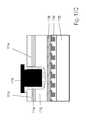
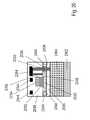
- FIG. 1illustrates a 3D integrated circuit.
- Silicon layer 0116could be thinned down from its original thickness, and its thickness could be in the range of approximatelylum to approximately 50 um.
- Silicon layer 0104may include transistors which could have gate electrode region 0114 , gate dielectric region 0112 , and shallow trench isolation (STI) regions 0110 .
- Silicon layer 0116may include transistors which could have gate electrode region 0134 , gate dielectric region 0132 , and shallow trench isolation (STI) regions 0130 .
- a through-silicon via (TSV) 0118could be present and may have a surrounding dielectric region 0120 .
- Wiring layers for silicon layer 0104are indicated as 0108 and wiring dielectric is indicated as 0106 .
- Wiring layers for silicon layer 0116are indicated as 0138 and wiring dielectric is indicated as 0136 .
- the heat removal apparatuswhich could include a heat spreader and a heat sink, is indicated as 0102 .
- the heat removal problem for the 3D integrated circuit shown in FIG. 1is immediately apparent.
- the silicon layer 0116is far away from the heat removal apparatus 0102 , and it is difficult to transfer heat between silicon layer 0116 and heat removal apparatus 0102 .
- wiring dielectric regions 0106do not conduct heat well, and this increases the thermal resistance between silicon layer 0116 and heat removal apparatus 0102 .
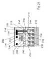
- FIG. 2illustrates a 3D integrated circuit that could be constructed, for example, using techniques described in U.S. patent application Ser. No. 12/900,379 and U.S. patent application Ser. No. 12/904,119.
- Two mono-crystalline silicon layers, 0204 and 0216are shown.
- Silicon layer 0216could be thinned down from its original thickness, and its thickness could be in the range of approximately 3 nm to approximately 1 um.
- Silicon layer 0204may include transistors which could have gate electrode region 0214 , gate dielectric region 0212 , and shallow trench isolation (STI) regions 0210 .
- Silicon layer 0216may include transistors which could have gate electrode region 0234 , gate dielectric region 0232 , and shallow trench isolation (STI) regions 0222 .
- STIshallow trench isolation
- STI regions 0222can go right through to the bottom of silicon layer 0216 and provide good electrical isolation. This, however, can cause challenges for heat removal from the STI surrounded transistors since STI regions 0222 are typically insulators that do not conduct heat well. Therefore, the heat spreading capabilities of silicon layer 0216 with STI regions 0222 are low.
- a through-layer via (TLV) 0218could be present and may include its dielectric region 0220 .
- Wiring layers for silicon layer 0204are indicated as 0208 and wiring dielectric is indicated as 0206 .
- Wiring layers for silicon layer 0216are indicated as 0238 and wiring dielectric is indicated as 0236 .
- the heat removal apparatuswhich could include a heat spreader and a heat sink, is indicated as 0202 .
- the heat removal problem for the 3D integrated circuit shown in FIG. 2is immediately apparent.
- the silicon layer 0216is far away from the heat removal apparatus 0202 , and it is difficult to transfer heat between silicon layer 0216 and heat removal apparatus 0202 .
- wiring dielectric regions 0206do not conduct heat well, and this increases the thermal resistance between silicon layer 0216 and heat removal apparatus 0202 .
- the heat removal challengeis further exacerbated by the poor heat spreading properties of silicon layer 0216 with STI regions 0222 .
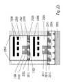
- FIG. 3 and FIG. 4illustrate how the power or ground distribution network of a 3D integrated circuit could assist heat removal.
- FIG. 3illustrates an exemplary power distribution network or structure of the 3D integrated circuit.
- the 3D integrated circuitcould, for example, be constructed with two silicon layers 0304 and 0316 .
- the heat removal apparatus 0302could include a heat spreader and a heat sink.
- the power distribution network or structurecould consist of a global power grid 0310 that takes the supply voltage (denoted as V DD ) from power pads and transfers it to local power grids 0308 and 0306 , which then transfer the supply voltage to logic cells or gates such as 0314 and 0315 .
- Vias 0318 and 0312could be used to transfer the supply voltage from the global power grid 0310 to local power grids 0308 and 0306 .
- the 3D integrated circuitcould have a similar distribution networks, such as for ground and other supply voltages, as well. Typically, many contacts are made between the supply and ground distribution networks and silicon layer 0304 . Due to this, there could exist a low thermal resistance between the power/ground distribution network and the heat removal apparatus 0302 . Since power/ground distribution networks are typically constructed of conductive metals and could have low effective electrical resistance, they could have a low thermal resistance as well.
- Each logic cell or gateon the 3D integrated circuit(such as, for example 0314 ) is typically connected to V DD and ground, and therefore could have contacts to the power and ground distribution network. These contacts could help transfer heat efficiently (i.e. with low thermal resistance) from each logic cell or gate on the 3D integrated circuit (such as, for example 0314 ) to the heat removal apparatus 0302 through the power/ground distribution network and the silicon layer 0304 .
- FIG. 4illustrates an exemplary NAND logic cell or gate 0420 and shows how all portions of thislogic cell or gate could be located with low thermal resistance to the V DD or ground (GND) contacts.
- the NAND gate 0420could consist of two pMOS transistors 0402 and two nMOS transistors 0404 .
- the layout of the NAND gate 0420is indicated in 0422 .
- Various regions of the layoutinclude metal regions 0406 , poly regions 0408 , n type silicon regions 0410 , p type silicon regions 0412 , contact regions 0414 , and oxide regions 0424 .
- pMOS transistors in the layoutare indicated as 0416 and nMOS transistors in the layout are indicated as 0418 .
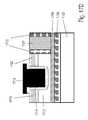
- FIG. 5describes an embodiment of this present invention, where the concept of thermal contacts is described.
- Two mono-crystalline silicon layers, 0504 and 0516may have transistors.
- Silicon layer 0516could be thinned down from its original thickness, and its thickness could be in the range of approximately 3 nm to approximately 1 um.
- Mono-crystalline silicon layer 0504could have STI regions 0510 , gate dielectric regions 0512 , gate electrode regions 0514 and several other regions required for transistors (not shown).
- Mono-crystalline silicon layer 0516could have STI regions 0530 , gate dielectric regions 0532 , gate electrode regions 0534 and several other regions required for transistors (not shown).
- Heat removal apparatus 0502may include, for example, heat spreaders and heat sinks. In the example shown in FIG.
- mono-crystalline silicon layer 0504is closer to the heat removal apparatus 0502 than other mono-crystalline silicon layers such as 0516 .
- Dielectric regions 0506 and 0546could be used to insulate wiring regions such as 0522 and 0542 respectively.
- Through-layer vias for power delivery 0518 and their associated dielectric regions 0520are shown.
- a thermal contact 0524can be used that connects the local power distribution network or structure, which may include wiring layers 0542 used for transistors in the silicon layer 0504 , to the silicon layer 0504 .
- Thermal junction 0526can be either a doped or undoped region of silicon, and further details of thermal junction 0526 will be given in FIG. 6 .
- the thermal contact such as 0524can be preferably placed close to the corresponding through-layer via for power delivery 0518 ; this helps transfer heat efficiently from the through-layer via for power delivery 0518 to thermal junction region 0526 and silicon layer 0504 and ultimately to the heat removal apparatus 0502 .
- the thermal contact 0524could be located within approximately 2 um distance of the through-layer via for power delivery 0518 in the X-Y plane (the through-layer via direction is considered the Z plane in FIG. 5 ). While the thermal contact such as 0524 is described above as being between the power distribution network or structure and the silicon layer closest to the heat removal apparatus, it could also be between the ground distribution network and the silicon layer closest to the heat sink.
- thermal contact 0524can be placed close to the through-layer via for power delivery 0518 .
- These thermal contactscan improve heat transfer from transistors located in higher layers of silicon such as 0516 to the heat removal apparatus 0502 .
- mono-crystalline siliconhas been mentioned as the transistor material in this paragraph, other options are possible including, for example, poly-crystalline silicon, mono-crystalline germanium, mono-crystalline III-V semiconductors, graphene, and various other semiconductor materials with which devices, such as transistors, may be constructed within.
- FIG. 6describes an embodiment of this present invention, where various implementations of thermal junctions and associated thermal contacts are illustrated.
- P-wells in CMOS integrated circuitsare typically biased to ground and N-wells are typically biased to the supply voltage V DD .
- V DDsupply voltage
- a thermal contact 0604 between the power (V DD ) distribution network and a P-well 0602can be implemented as shown in N+ in P-well thermal junction and contact example 0608 , where an n+ doped region thermal junction 0606 is formed in the P-well region at the base of the thermal contact 0604 .
- the n+ doped region thermal junction 0606ensures a reverse biased p-n junction can be formed in N+ in P-well thermal junction and contact example 0608 and makes the thermal contact viable (i.e. not highly conductive) from an electrical perspective.
- the thermal contact 0604could be formed of a conductive material such as copper, aluminum or some other material.
- a thermal contact 0614 between the ground (GND) distribution network and a P-well 0612can be implemented as shown in P+ in P-well thermal junction and contact example 0618 , where a p+ doped region thermal junction 0616 may be formed in the P-well region at the base of the thermal contact 0614 .
- the p+ doped region thermal junction 0616makes the thermal contact viable (i.e. not highly conductive) from an electrical perspective.
- the p+ doped region thermal junction 0616 and the P-well 0612would typically be biased at ground potential.
- a thermal contact 0624 between the power (V DD ) distribution network and an N-well 0622can be implemented as shown in N+ in N-well thermal junction and contact example 0628 , where an n+ doped region thermal junction 0626 may be formed in the N-well region at the base of the thermal contact 0624 .
- the n+ doped region thermal junction 0626makes the thermal contact viable (i.e. not highly conductive) from an electrical perspective. Both the n+ doped region thermal junction 0626 and the N-well 0622 would typically be biased at V DD potential.
- a thermal contact 0634 between the ground (GND) distribution network and an N-well 0632can be implemented as shown in P+ in N-well thermal junction and contact example 0638 , where a p+ doped region thermal junction 0636 may be formed in the N-well region at the base of the thermal contact 0634 .
- the p+ doped region thermal junction 0636makes the thermal contact viable (i.e. not highly conductive) from an electrical perspective due to the reverse biased p-n junction formed in P+ in N-well thermal junction and contact example 0638 .
- the thermal contactsare designed to conduct negligible electricity, and the current flowing through them is several orders of magnitude lower than the current flowing through a transistor when it is switching. Therefore, the thermal contacts can be considered to be designed to conduct heat and conduct negligible (or no) electricity.
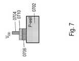
- FIG. 7describes an embodiment of this present invention, where an additional type of thermal contact structure is illustrated.
- the embodiment shown in FIG. 7could also function as a decoupling capacitor to mitigate power supply noise. It could consist of a thermal contact 0704 , an electrode 0710 , a dielectric 0706 and P-well 0702 .
- the dielectric 0706may be electrically insulating, and could be optimized to have high thermal conductivity.
- Dielectric 0706could be formed of materials, such as, for example, hafnium oxide, silicon dioxide, other high k dielectrics, carbon, carbon based material, or various other dielectric materials with electrical conductivity below 1 nano-amp per square micron.
- a thermal connectionmay be defined as the combination of a thermal contact and a thermal junction.
- the thermal connections illustrated in FIG. 6 , FIG. 7 and other figures in this patent applicationare designed into a chip to remove heat, and are not designed to conduct electricity.
- a semiconductor devicecomprising power distribution wires is described wherein some of said wires have a thermal connection designed to conduct heat to the semiconductor layer but the wires do not substantially conduct electricity through the thermal connection to the semiconductor layer.
- Thermal contacts similar to those illustrated in FIG. 6 and FIG. 7can be used in the white spaces of a design, i.e. locations of a design where logic gates or other useful functionality are not present. These thermal contacts connect white-space silicon regions to power and/or ground distribution networks. Thermal resistance to the heat removal apparatus can be reduced with this approach. Connections between silicon regions and power/ground distribution networks can be used for various device layers in the 3D stack, and need not be restricted to the device layer closest to the heat removal apparatus. A Schottky contact or diode may also be utilized for a thermal contact and thermal junction.
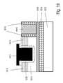
- FIG. 8illustrates an embodiment of this invention, which can provide enhanced heat removal from 3D-ICs by integrating heat spreader regions in stacked device layers.
- Two mono-crystalline silicon layers, 0804 and 0816are shown.
- Silicon layer 0816could be thinned from its original thickness, and its thickness could be in the range of approximately 3 nm to approximately 1 um.
- Silicon layer 0804may include gate electrode region 0814 , gate dielectric region 0812 , and shallow trench isolation (STI) regions 0810 .
- Silicon layer 0816may include gate electrode region 0834 , gate dielectric region 0832 , and shallow trench isolation (STI) regions 0822 .
- a through-layer via (TLV) 0818could be present and may have a dielectric region 0820 .
- TLVthrough-layer via
- Wiring layers for silicon layer 0804are indicated as 0808 and wiring dielectric is indicated as 0806 .
- Wiring layers for silicon layer 0816are indicated as 0838 and wiring dielectric is indicated as 0836 .
- the heat removal apparatuswhich could include a heat spreader and a heat sink, is indicated as 0802 . It can be observed that the STI regions 0822 can go right through to the bottom of silicon layer 0816 and provide good electrical isolation. This, however, can cause challenges for heat removal from the STI surrounded transistors since STI regions 0822 are typically insulators that do not conduct heat well. The buried oxide layer 0824 typically does not conduct heat well either. To tackle heat removal issues with the structure shown in FIG. 8 , a heat spreader 0826 can be integrated into the 3D stack.
- the heat spreader 0826 materialmay include, for example, copper, aluminum, graphene, diamond, carbon or any other material with a high thermal conductivity (defined as greater than 100 W/m-K). While the heat spreader concept for 3D-ICs is described with an architecture similar to FIG. 2 , similar heat spreader concepts could be used for architectures similar to FIG. 1 , and also for other 3D IC architectures.
- FIG. 9illustrates an embodiment of this present invention, which can provide enhanced heat removal from 3D-ICs by using thermally conductive shallow trench isolation (STI) regions in stacked device layers.
- Two mono-crystalline silicon layers, 0904 and 0916are shown.
- Silicon layer 0916could be thin, and its thickness could be in the range of approximately 3 nm to approximately 1 um.
- Silicon layer 0904may include transistors which could have gate electrode region 0914 , gate dielectric region 0912 , and shallow trench isolation (STI) regions 0910 .
- Silicon layer 0916may include transistors which could have gate electrode region 0934 , gate dielectric region 0932 , and shallow trench isolation (STI) regions 0922 .
- a through-layer via (TLV) 0918could be present and may have a dielectric region 0920 .
- TLVthrough-layer via
- Dielectric region 0920may include a shallow trench isolation region.
- Wiring layers for silicon layer 0904are indicated as 0908 and wiring dielectric is indicated as 0906 .
- Wiring layers for silicon layer 0916are indicated as 0938 and wiring dielectric is indicated as 0936 .
- the heat removal apparatuswhich could include a heat spreader and a heat sink, is indicated as 0902 . It can be observed that the STI regions 0922 can go right through to the bottom of silicon layer 0916 and provide good electrical isolation. This, however, can cause challenges for heat removal from the STI surrounded transistors since STI regions 0922 are typically filled with insulators such as silicon dioxide that do not conduct heat well. To tackle possible heat removal issues with the structure shown in FIG.
- the STI regions 0922 in stacked silicon layers such as 0916could be formed substantially of thermally conductive dielectrics including, for example, diamond, carbon, or other dielectrics that have a thermal conductivity higher than silicon dioxide. Essentially, these materials could have thermal conductivity higher than 0.6 W/m-K. This can provide enhanced heat spreading in stacked device layers. Essentially, thermally conductive STI dielectric regions could be used in the vicinity of the transistors in stacked 3D device layers and may also be utilized as the dielectric that surrounds TLV 0918 , such as dielectric region 0920 .
- FIG. 10illustrates an embodiment of this present invention, which can provide enhanced heat removal from 3D-ICs using thermally conductive pre-metal dielectric regions in stacked device layers.
- Two mono-crystalline silicon layers, 1004 and 1016are shown.
- Silicon layer 1016could be thin, and its thickness could be in the range of approximately 3 nm to approximately 1 um.
- Silicon layer 1004may include transistors which could have gate electrode region 1014 , gate dielectric region 1012 , and shallow trench isolation (STI) regions 1010 .
- Silicon layer 1016may include transistors which could have gate electrode region 1034 , gate dielectric region 1032 , and shallow trench isolation (STI) regions 1022 .
- STIshallow trench isolation
- a through-layer via (TLV) 1018could be present and may have a dielectric region 1020 , which may include an STI region.
- Wiring layers for silicon layer 1004are indicated as 1008 and wiring dielectric is indicated as 1006 .
- Wiring layers for silicon layer 1016are indicated as 1038 and wiring dielectric is indicated as 1036 .
- the heat removal apparatuswhich could include a heat spreader and a heat sink, is indicated as 1002 . It can be observed that the STI regions 1022 can go right through to the bottom of silicon layer 1016 and provide good electrical isolation. This, however, can cause challenges for heat removal from the STI surrounded transistors since STI regions 1022 are typically filled with insulators such as silicon dioxide that do not conduct heat well.
- the inter-layer dielectrics (ILD) 1024 for contact region 1026could be constructed substantially with a thermally conductive material, such as, for example, insulating carbon, diamond, diamond like carbon (DLC), and various other materials that provide better thermal conductivity than silicon dioxide. Essentially, these materials could have thermal conductivity higher than 0.6 W/m-K. Essentially, thermally conductive pre-metal dielectric regions could be used around some of the transistors in stacked 3D device layers.
- a thermally conductive materialsuch as, for example, insulating carbon, diamond, diamond like carbon (DLC), and various other materials that provide better thermal conductivity than silicon dioxide. Essentially, these materials could have thermal conductivity higher than 0.6 W/m-K. Essentially, thermally conductive pre-metal dielectric regions could be used around some of the transistors in stacked 3D device layers.
- FIG. 11describes an embodiment of this present invention, which can provide enhanced heat removal from 3D-ICs using thermally conductive etch stop layers or regions for the first metal level of stacked device layers.
- Two mono-crystalline silicon layers, 1104 and 1116are shown. Silicon layer 1116 could be thin, and its thickness could be in the range of approximately 3 nm to approximately 1 um. Silicon layer 1104 may include transistors which could have gate electrode region 1114 , gate dielectric region 1112 , and shallow trench isolation (STI) regions 1110 . Silicon layer 1116 may include transistors which could have gate electrode region 1134 , gate dielectric region 1132 , and shallow trench isolation (STI) regions 1122 .
- a through-layer via (TLV) 1118could be present and may include dielectric region 1120 .
- Wiring layers for silicon layer 1104are indicated as 1108 and wiring dielectric is indicated as 1106 .
- Wiring layers for silicon layer 1116are indicated as first metal layer 1128 and other metal layers 1138 and wiring dielectric is indicated as 1136 .
- the heat removal apparatuswhich could include a heat spreader and a heat sink, is indicated as 1102 . It can be observed that the STI regions 1122 can go right through to the bottom of silicon layer 1116 and provide good electrical isolation. This, however, can cause challenges for heat removal from the STI surrounded transistors since STI regions 1122 are typically filled with insulators such as silicon dioxide that do not conduct heat well.
- etch stop layer 1124 for the first metal layer 1128 of stacked device layerscan be substantially constructed out of a thermally conductive but electrically isolative material.
- thermally conductive materialscould include insulating carbon, diamond, diamond like carbon (DLC), and various other materials that provide better thermal conductivity than silicon dioxide and silicon nitride. Essentially, these materials could have thermal conductivity higher than 0.6 W/m-K.
- thermally conductive etch-stop layer dielectric regionscould be used for the first metal layer above transistors in stacked 3D device layers.
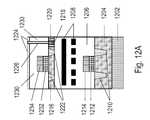
- FIG. 12A-Bdescribes an embodiment of this present invention, which can provide enhanced heat removal from 3D-ICs using thermally conductive layers or regions as part of pre-metal dielectrics for stacked device layers.
- Two mono-crystalline silicon layers, 1204 and 1216are shown and may have transistors.
- Silicon layer 1216could be thin, and its thickness could be in the range of approximately 3 nm to approximately 1 um.
- Silicon layer 1204could have gate electrode region 1214 , gate dielectric region 1212 and shallow trench isolation (STI) regions 1210 .
- Silicon layer 1216could have gate electrode region 1234 , gate dielectric region 1232 and shallow trench isolation (STI) regions 1222 .
- a through-layer via (TLV) 1218could be present and may include its dielectric region 1220 .
- Wiring layers for silicon layer 1204are indicated as 1208 and wiring dielectric is indicated as 1206 .
- the heat removal apparatuswhich could include a heat spreader and a heat sink, is indicated as 1202 . It can be observed that the STI regions 1222 can go right through to the bottom of silicon layer 1216 and provide good electrical isolation. This, however, can cause challenges for heat removal from the STI surrounded transistors since STI regions 1222 are typically filled with insulators such as silicon dioxide that do not conduct heat well. To tackle this issue, a technique is described in FIG. 12A-B .
- FIG. 12Aillustrates the formation of openings for making contacts to transistors.
- a hard mask layer 1224is typically used during the lithography step for contact formation and this hard mask 1224 is utilized to define regions 1226 of the pre-metal dielectric 1230 that are etched away.
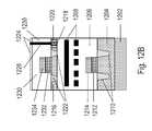
- FIG. 12Bshows the contact 1228 formed after metal is filled into the contact opening 1226 shown in FIG. 12A , and after a chemical mechanical polish (CMP) process.
- the hard mask 1224 used for the process shown in FIG. 12A-Bcan be chosen to be a thermally conductive material such as, for example, carbon or other material with higher thermal conductivity than silicon nitride, and can be left behind after the process step shown in FIG. 12B . Essentially, these materials for hard mask 1224 could have a thermal conductivity higher than 0.6 W/m-K. Further steps for forming the 3D-IC (such as forming additional metal layers) can then be performed.
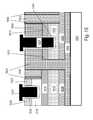
- FIG. 13shows the layout of a 4 input NAND gate, where the output OUT is a function of inputs A, B, C and D.
- Various sections of the 4 input NAND gatecould include metal 1 regions 1306 , gate regions 1308 , N-type silicon regions 1310 , P-type silicon regions 1312 , contact regions 1314 , and oxide isolation regions 1316 .
- some regions of the NAND gate(such as 1318 ) are far away from V DD and GND contacts, these regions could have high thermal resistance to V DD and GND contacts, and could heat up to undesired temperatures. This is because the regions of the NAND gate that are far away from V DD and GND contacts cannot effectively use the low-thermal resistance power delivery network to transfer heat to the heat removal apparatus.
- FIG. 14illustrates an embodiment of this present invention wherein the layout of the 3D stackable 4 input NAND gate can be modified so that all parts of the gate are atdesirable, such as sub-100° C., temperatures during chip operation.
- Inputs to the gateare denoted as A, B, C and D, and the output is denoted as OUT.
- Various sections of the 4 input NAND gatecould include the metal 1 regions 1406 , gate regions 1408 , N-type silicon regions 1410 , P-type silicon regions 1412 , contact regions 1414 , and oxide isolation regions 1416 .
- An additional thermal contact 1420(whose implementation can be similar to those described in FIG. 6 and FIG. 7 ) can be added to the layout shown in FIG. 13 to keep the temperature of region 1418 under desirable limits (by reducing the thermal resistance from region 1418 to the GND distribution network).
- Several other techniquescan also be used to make the layout shown in FIG. 14 more desirable from a thermal perspective.
- FIG. 15shows the layout of a transmission gate with inputs A and A′.
- Various sections of the transmission gatecould include metal 1 regions 1506 , gate regions 1508 , N-type silicon regions 1510 , P-type silicon regions 1512 , contact regions 1514 , and oxide isolation regions 1516 . If the transmission gate is used in 3D IC stacked device layers, many regions of the transmission gate could heat up to undesired temperatures since there are no V DD and GND contacts. So, there could be high thermal resistance to V DD and GND distribution networks. Thus, the transmission gate cannot effectively use the low-thermal resistance power delivery network to transfer heat to the heat removal apparatus.
- FIG. 16illustrates an embodiment of this present invention wherein the layout of the 3D stackable transmission gate can be modified so that all parts of the gate are at desirable, such as sub-100° C., temperatures during chip operation.
- Inputs to the gateare denoted as A and A′.
- Various sections of the transmission gatecould include metal 1 regions 1606 , gate regions 1608 , N-type silicon regions 1610 , P-type silicon regions 1612 , contact regions 1614 , and oxide isolation regions 1616 .
- Additional thermal contactssuch as, for example 1620 and 1622 (whose implementation can be similar to those described in FIG. 6 and FIG. 7 ) can be added to the layout shown in FIG. 15 to keep the temperature of the transmission gate under desirable limits (by reducing the thermal resistance to the V DD and GND distribution networks).
- Several other techniquescan also be used to make the layout shown in FIG. 16 more desirable from a thermal perspective.
- the techniques illustrated with FIG. 14 and FIG. 16are not restricted to cells such as transmission gates and NAND gates, and can be applied to a number of cells such as, for example, SRAMs, CAMs, multiplexers and many others. Furthermore, the techniques illustrated with FIG. 14 and FIG. 16 can be applied and adapted to various techniques of constructing 3D integrated circuits and chips, including those described in pending U.S. patent application Ser. No. 12/900,379 and U.S. patent application Ser. No. 12/904,119. Furthermore, techniques illustrated with FIG. 14 and FIG. 16 (and other similar techniques) need not be applied to all such gates on the chip, but could be applied to a portion of gates of that type, such as, for example, gates with higher activity factor, lower threshold voltage or higher drive current.
- a cell libraryconsisting of various logic cells such as NAND gates, NOR gates and other gates is created, and the chip design flow proceeds using this cell library. It will be clear to one skilled in the art that one can create a cell library where each cell's layout can be optimized from a thermal perspective (i.e. where each cell's layout can be optimized such that all portions of the cell have low thermal resistance to the V DD and GND contacts).
- Recessed channel transistorsform a transistor family that can be stacked in 3D.
- FIG. 22illustrates a Recessed Channel Transistor when constructed in a 3D stacked layer using procedures outlined in pending U.S. patent application Ser. No. 12/900,379 and pending U.S. patent application Ser. No. 12/804,119.
- 2202could indicate a bottom layer of transistors and wires
- 2204could indicate an oxide layer
- 2206could indicate oxide regions
- 2208could indicate a gate dielectric
- 2210could indicate n+ silicon regions
- 2212could indicate a gate electrode
- 2214could indicate a region of p ⁇ silicon.
- FIG. 17A-Dillustrates an embodiment of this present invention where thermal contacts can be constructed to a recessed channel transistor.
- numbers used in FIG. 17A-Dare inter-related. For example, if a certain number is used in FIG. 17A , it has the same meaning if present in FIG. 17B .
- the process flowbegins in FIG. 17A with a bottom layer of transistors and copper interconnects 1702 being constructed with a silicon dioxide layer 1704 atop it. Using layer transfer approaches similar to those described in pending U.S. patent application Ser. Nos.
- FIG. 17Cshows the next step in the process flow. After forming isolation regions (not shown in FIG. 17C for simplicity), gate dielectric regions 1716 and gate electrode regions 1718 could be formed using procedures similar to those described in pending U.S. patent application Ser. Nos. 12/800,379 and 12/904,119. 1712 could indicate a region of p ⁇ silicon and 1714 could indicate a region of n+ silicon.
- FIG. 1712could indicate a region of p ⁇ silicon and 1714 could indicate a region of n+ silicon.
- FIG. 17Cthus shows a RCAT (recessed channel transistor) formed with a p+ silicon region atop copper interconnect regions where the copper interconnect regions are not exposed to temperatures higher than approximately 400° C.
- FIG. 17Dshows the next step of the process where thermal contacts could be made to the p+ silicon region 1706 .
- 1722could indicate a region of p ⁇ silicon
- 1720could indicate a region of n+ silicon
- 1724could indicate a via constructed of a metal or metal silicide or a combination of the two and 1726 could indicate oxide regions.
- Via 1724can connect p+ region 1706 to the ground (GND) distribution network. This is because the nMOSFET could have its body region connected to GND potential and operate correctly or as desired, and the heat produced in the device layer can be removed through the low-thermal resistance GND distribution network to the heat removal apparatus.
- GNDground
- FIG. 18illustrates an embodiment of this present invention, which illustrates the application of thermal contacts to remove heat from a pMOSFET device layer that is stacked above a bottom layer of transistors and wires 1802 .
- 1804represents a buried oxide region
- 1806represents an n+ region of mono-crystalline silicon
- 1814represents an n ⁇ region of mono-crystalline silicon
- 1810represents a p+ region of mono-crystalline silicon
- 1808represents the gate dielectric
- 1812represents the gate electrode.
- the structure shown in FIG. 18can be constructed using methods similar to those described in pending U.S. patent application Ser. No. 12/900,379, U.S. patent application Ser. No. 12/904,119 and FIG. 17A-D .
- the thermal contact 1818could be constructed of any metal, metal silicide or a combination of these two types of materials. It can connect n+ region 1806 to the power (V DD ) distribution network. This is because the pMOSFET could have its body region connected to the supply voltage (V DD ) potential and operate correctly or as desired, and the heat produced in the device layer can be removed through the low-thermal resistance V DD distribution network to the heat removal apparatus. Regions 1816 represent isolation regions.
- FIG. 19illustrates an embodiment of this present invention that describes the application of thermal contacts to remove heat from a CMOS device layer that could be stacked atop a bottom layer of transistors and wires 1902 .
- FIGS. 19 , 1904 , 1924 and 1930could represent regions of an insulator, such as silicon dioxide, 1906 and 1936 could represent regions of p+ silicon, 1908 and 1912 could represent regions of p ⁇ silicon, 1910 could represent regions of n+ silicon, 1914 could represent regions of n+ silicon, 1916 could represent regions of n ⁇ silicon, 1920 could represent regions of p+ silicon, 1918 could represent a gate dielectric region for a pMOS transistor, 1922 could represent a gate electrode region for a pMOS transistor, 1934 could represent a gate dielectric region for a nMOS transistor and 1928 could represent a gate electrode region for a nMOS transistor.
- an insulatorsuch as silicon dioxide
- 1906 and 1936could represent regions of p+ silicon
- 1908 and 1912could represent regions of p
- a nMOS transistorcould therefore be formed of regions 1934 , 1928 , 1910 , 1908 and 1906 .
- a pMOS transistorcould therefore be formed of regions 1914 , 1916 , 1918 , 1920 and 1922 .
- This stacked CMOS device layercould be formed with procedures similar to those described in pending U.S. patent application Ser. No. 12/900,379, U.S. patent application Ser. No. 12/904,119 and FIG. 17A-D .
- the thermal contact 1926 connected between n+ silicon region 1914 and the power (V DD ) distribution networkhelps remove heat from the pMOS transistor.
- the pMOSFETcould have its body region connected to the supply voltage (V DD ) potential and operate correctly or as desired, and the heat produced in the device layer can be removed through the low-thermal resistance V DD distribution network to the heat removal apparatus as previously described.
- the thermal contact 1932 connected between p+ silicon region 1906 and the ground (GND) distribution networkhelps remove heat from the nMOS transistor. This is because the nMOSFET could have its body region connected to GND potential and operate correctly or as desired, and the heat produced in the device layer can be removed through the low-thermal resistance GND distribution network to the heat removal apparatus as previously described.
- FIG. 20illustrates an embodiment of this present invention that describes a technique that could reduce heat-up of transistors fabricated on silicon-on-insulator (SOI) substrates.
- SOI substrateshave a buried oxide (BOX) between the silicon transistor regions and the heat sink. This BOX region has a high thermal resistance, and makes heat transfer from transistor regions to the heat sink difficult.
- BOXburied oxide
- 20 , 2036 , 2048 and 2056could represent regions of an insulator, such as silicon dioxide, 2046 could represent regions of n+ silicon, 2040 could represent regions of p ⁇ silicon, 2052 could represent a gate dielectric region for a nMOS transistor, 2054 could represent a gate electrode region for a nMOS transistor, 2044 could represent copper wiring regions and 2004 could represent a highly doped silicon region.
- SOIsilicon-on-insulator
- FIG. 20can be connected to the ground distribution network 2064 which in turn can be connected with a low thermal resistance connection 2050 to substrate 2004 .
- Thisenables low thermal conductivity between the transistor shown in FIG. 20 and the heat removal apparatus 2002 . While FIG. 20 described how heat could be transferred between an MOS transistor and the heat removal apparatus, similar approaches can also be used for pMOS transistors.
- FIG. 21illustrates an embodiment of this present invention that describes a technique that could reduce heat-up of transistors fabricated on silicon-on-insulator (SOI) substrates.
- SOIsilicon-on-insulator
- FIGS. 21 , 2136 , 2148 and 2156could represent regions of an insulator, such as silicon dioxide
- 2146could represent regions of n+ silicon
- 2140could represent regions of p ⁇ silicon
- 2152could represent a gate dielectric region for a nMOS transistor
- 2154could represent a gate electrode region for a nMOS transistor
- 2144could represent copper wiring regions
- 2104could represent a doped silicon region.
- silicon-on-insulator (SOI) substratesOne of the key limitations of silicon-on-insulator (SOI) substrates is the low heat transfer from transistor regions to the heat removal apparatus 2102 through the buried oxide layer 2136 that has low thermal conductivity.
- the ground contact 2162 of the nMOS transistor shown in FIG. 21can be connected to the ground distribution network 2164 which in turn can be connected with a low thermal resistance connection 2150 to substrate 2104 through an implanted and activated region 2110 .
- the implanted and activated region 2110could be such that thermal contacts similar to those in FIG. 6 can be formed. This could enable low thermal conductivity between the transistor shown in FIG. 21 and the heat removal apparatus 2102 . While FIG. 21 described how heat could be transferred between a nMOS transistor and the heat removal apparatus, similar approaches can also be used for pMOS transistors.
- FIG. 23illustrates an embodiment of this invention that could have heat spreading regions located on the sides of 3D-ICs.
- the 3D integrated circuit shown in FIG. 23could be potentially constructed using techniques described in U.S. patent application Ser. No. 12/900,379 and U.S. patent application Ser. No. 12/904,119.
- Two mono-crystalline silicon layers, 2304 and 2316are shown. Silicon layer 2316 could be thinned down from its original thickness, and its thickness could be in the range of approximately 3 nm to approximately 1 um.
- Silicon layer 2304may include transistors which could have gate electrode region 2314 , gate dielectric region 2312 , and shallow trench isolation (STI) regions 2310 .
- STIshallow trench isolation
- Silicon layer 2316may include transistors which could have gate electrode region 2334 , gate dielectric region 2332 , and shallow trench isolation (STI) regions 2322 . It can be observed that the STI regions 2322 can go right through to the bottom of silicon layer 2316 and provide good electrical isolation.
- a through-layer via (TLV) 2318could be present and may include its dielectric region 2320 .
- Wiring layers for silicon layer 2304are indicated as 2308 and wiring dielectric is indicated as 2306 .
- Wiring layers for silicon layer 2316are indicated as 2338 and wiring dielectric is indicated as 2336 .
- the heat removal apparatuswhich could include a heat spreader and a heat sink, is indicated as 2302 .
- Thermally conductive material 2340could be present at the sides of the 3D-IC shown in FIG. 23 .
- a thermally conductive heat spreading regioncould be located on the sidewalls of a 3D-IC.
- the thermally conductive material 2340could be a dielectric such as, for example, insulating carbon, diamond, diamond like carbon (DLC), and various other materials that provide better thermal conductivity than silicon dioxide. Essentially, these materials could have thermal conductivity higher than 0.6 W/m-K.
- One possible scheme that could be used for forming these regionscould involve depositing and planarizing the thermally conductive material 2340 at locations on or close to the dicing regions, such as potential dicing scribe lines, of a 3D-IC after an etch process. The wafer could then be diced.
Landscapes
- Engineering & Computer Science (AREA)
- Chemical & Material Sciences (AREA)
- Materials Engineering (AREA)
- Physics & Mathematics (AREA)
- Condensed Matter Physics & Semiconductors (AREA)
- General Physics & Mathematics (AREA)
- Computer Hardware Design (AREA)
- Microelectronics & Electronic Packaging (AREA)
- Power Engineering (AREA)
- Internal Circuitry In Semiconductor Integrated Circuit Devices (AREA)
- Design And Manufacture Of Integrated Circuits (AREA)
Abstract
Description
- 1. Field of the Invention
- The present invention relates to the general field of Integrated Circuit (IC) devices and fabrication methods, and more particularly to multilayer or Three Dimensional Integrated Circuit (3D-IC) devices.
- 2. Discussion of Background Art
- Over the past 40 years, there has been a dramatic increase in functionality and performance of Integrated Circuits (ICs). This has largely been due to the phenomenon of “scaling”; i.e., component sizes within ICs have been reduced (“scaled”) with every successive generation of technology. There are two main classes of components in Complementary Metal Oxide Semiconductor (CMOS) ICs, namely transistors and wires. With “scaling”, transistor performance and density typically improve and this has contributed to the previously-mentioned increases in IC performance and functionality. However, wires (interconnects) that connect together transistors degrade in performance with “scaling”. The situation today is that wires dominate performance, functionality and power consumption of ICs.
- 3D stacking of semiconductor devices or chips is one avenue to tackle the issues with wires. By arranging transistors in 3 dimensions instead of 2 dimensions (as was the case in the 1990s), the transistors in ICs can be placed closer to each other. This reduces wire lengths and keeps wiring delay low.
- There are many techniques to construct 3D stacked integrated circuits or chips including:
- Through-silicon via (TSV) technology: Multiple layers of transistors (with or without wiring levels) can be constructed separately. Following this, they can be bonded to each other and connected to each other with through-silicon vias (TSVs).
- Monolithic 3D technology: With this approach, multiple layers of transistors and wires can be monolithically constructed. Some monolithic 3D approaches are described in pending U.S. patent application Ser. No. 12/900,379 and U.S. patent application Ser. No. 12/904,119.
- Irrespective of the technique used to construct 3D stacked integrated circuits or chips, heat removal is a serious issue for this technology. For example, when a layer of circuits with power density P is stacked atop another layer with power density P, the net power density is 2P. Removing the heat produced due to this power density is a significant challenge. In addition, many heat producing regions in 3D stacked integrated circuits or chips have a high thermal resistance to the heat sink, and this makes heat removal even more difficult.
- Several solutions have been proposed to tackle this issue of heat removal in 3D stacked integrated circuits and chips. These are described in the following paragraphs.
- Many publications have suggested passing liquid coolant through multiple device layers of a 3D-IC to remove heat. This is described in“Microchannel Cooled 3D Integrated Systems”, Proc. Intl. Interconnect Technology Conference, 2008 by D.C. Sekar, et al and “Forced Convective Interlayer Cooling in Vertically Integrated Packages,” Proc. Intersoc. Conference on Thermal Management (ITHERM), 2008 by T. Brunschweiler, et al.
- Thermal vias have been suggested as techniques to transfer heat from stacked device layers to the heat sink. Use of power and ground vias for thermal conduction in 3D-ICs has also been suggested. These techniques are described in “Allocating Power Ground Vias in 3D ICs for Simultaneous Power and Thermal Integrity” ACM Transactions on Design Automation of Electronic Systems (TODAES), May 2009 by Hao Yu, Joanna Ho and Lei He.
- Other techniques to remove heat from 3D Integrated Circuits and Chips will be beneficial.
- Various embodiments of the present invention will be understood and appreciated more fully from the following detailed description, taken in conjunction with the drawings in which:
FIG. 1 is a drawing illustration of a 3D integrated circuit;FIG. 2 is a drawing illustration of another 3D integrated circuit;FIG. 3 is a drawing illustration of the power distribution network of a 3D integrated circuit;FIG. 4 is a drawing illustration of a NAND gate;FIG. 5 is a drawing illustration of the thermal contact concept;FIG. 6 is a drawing illustration of various types of thermal contacts;FIG. 7 is a drawing illustration of another type of thermal contact;FIG. 8 illustrates the use of heat spreaders in 3D stacked device layers;FIG. 9 illustrates the use of thermally conductive shallow trench isolation (STI) in 3D stacked device layers;FIG. 10 illustrates the use of thermally conductive pre-metal dielectric regions in 3D stacked device layers;FIG. 11 illustrates the use of thermally conductive etch stop layers for the first metal layer of 3D stacked device layers;FIG. 12A-B illustrate the use and retention of thermally conductive hard mask layers for patterning contact layers of 3D stacked device layers;FIG. 13 is a drawing illustration of a 4 input NAND gate;FIG. 14 is a drawing illustration of a 4 input NAND gate where all parts of the logic cell can be within desirable temperature limits;FIG. 15 is a drawing illustration of a transmission gate; andFIG. 16 is a drawing illustration of a transmission gate where all parts of the logic cell can be within desirable temperature limits;FIG. 17A-D is a process flow for constructing recessed channel transistors with thermal contacts;FIG. 18 is a drawing illustration of a pMOS recessed channel transistor with thermal contacts;FIG. 19 is a drawing illustration of a CMOS circuit with recessed channel transistors and thermal contacts;FIG. 20 is a drawing illustration of a technique to remove heat more effectively from silicon-on-insulator (SOI) circuits;FIG. 21 is a drawing illustration of an alternative technique to remove heat more effectively from silicon-on-insulator (SOI) circuits;FIG. 22 is a drawing illustration of a recessed channel transistor (RCAT); andFIG. 23 is a drawing illustration of a 3D-IC with thermally conductive material on the sides.- Embodiments of the present invention are now described with reference to the drawing figures. Persons of ordinary skill in the art will appreciate that the description and figures illustrate rather than limit the invention and that in general the figures are not drawn to scale for clarity of presentation. Such skilled persons will also realize that many more embodiments are possible by applying the inventive principles contained herein and that such embodiments fall within the scope of the invention which is not to be limited except by the appended claims.
FIG. 1 illustrates a 3D integrated circuit. Two mono-crystalline silicon layers,0104 and0116 are shown.Silicon layer 0116 could be thinned down from its original thickness, and its thickness could be in the range of approximatelylum to approximately 50 um.Silicon layer 0104 may include transistors which could havegate electrode region 0114,gate dielectric region 0112, and shallow trench isolation (STI)regions 0110.Silicon layer 0116 may include transistors which could havegate electrode region 0134,gate dielectric region 0132, and shallow trench isolation (STI)regions 0130. A through-silicon via (TSV)0118 could be present and may have a surroundingdielectric region 0120. Wiring layers forsilicon layer 0104 are indicated as0108 and wiring dielectric is indicated as0106. Wiring layers forsilicon layer 0116 are indicated as0138 and wiring dielectric is indicated as0136. The heat removal apparatus, which could include a heat spreader and a heat sink, is indicated as0102. The heat removal problem for the 3D integrated circuit shown inFIG. 1 is immediately apparent. Thesilicon layer 0116 is far away from theheat removal apparatus 0102, and it is difficult to transfer heat betweensilicon layer 0116 andheat removal apparatus 0102. Furthermore, wiringdielectric regions 0106 do not conduct heat well, and this increases the thermal resistance betweensilicon layer 0116 andheat removal apparatus 0102.FIG. 2 illustrates a 3D integrated circuit that could be constructed, for example, using techniques described in U.S. patent application Ser. No. 12/900,379 and U.S. patent application Ser. No. 12/904,119. Two mono-crystalline silicon layers,0204 and0216 are shown.Silicon layer 0216 could be thinned down from its original thickness, and its thickness could be in the range of approximately 3 nm to approximately 1 um.Silicon layer 0204 may include transistors which could havegate electrode region 0214,gate dielectric region 0212, and shallow trench isolation (STI)regions 0210.Silicon layer 0216 may include transistors which could havegate electrode region 0234,gate dielectric region 0232, and shallow trench isolation (STI)regions 0222. It can be observed that theSTI regions 0222 can go right through to the bottom ofsilicon layer 0216 and provide good electrical isolation. This, however, can cause challenges for heat removal from the STI surrounded transistors sinceSTI regions 0222 are typically insulators that do not conduct heat well. Therefore, the heat spreading capabilities ofsilicon layer 0216 withSTI regions 0222 are low. A through-layer via (TLV)0218 could be present and may include itsdielectric region 0220. Wiring layers forsilicon layer 0204 are indicated as0208 and wiring dielectric is indicated as0206. Wiring layers forsilicon layer 0216 are indicated as0238 and wiring dielectric is indicated as0236. The heat removal apparatus, which could include a heat spreader and a heat sink, is indicated as0202. The heat removal problem for the 3D integrated circuit shown inFIG. 2 is immediately apparent. Thesilicon layer 0216 is far away from theheat removal apparatus 0202, and it is difficult to transfer heat betweensilicon layer 0216 andheat removal apparatus 0202. Furthermore, wiringdielectric regions 0206 do not conduct heat well, and this increases the thermal resistance betweensilicon layer 0216 andheat removal apparatus 0202. The heat removal challenge is further exacerbated by the poor heat spreading properties ofsilicon layer 0216 withSTI regions 0222.FIG. 3 andFIG. 4 illustrate how the power or ground distribution network of a 3D integrated circuit could assist heat removal.FIG. 3 illustrates an exemplary power distribution network or structure of the 3D integrated circuit. The 3D integrated circuit, could, for example, be constructed with twosilicon layers heat removal apparatus 0302 could include a heat spreader and a heat sink. The power distribution network or structure could consist of aglobal power grid 0310 that takes the supply voltage (denoted as VDD) from power pads and transfers it tolocal power grids Vias global power grid 0310 tolocal power grids silicon layer 0304. Due to this, there could exist a low thermal resistance between the power/ground distribution network and theheat removal apparatus 0302. Since power/ground distribution networks are typically constructed of conductive metals and could have low effective electrical resistance, they could have a low thermal resistance as well. Each logic cell or gateon the 3D integrated circuit (such as, for example0314) is typically connected to VDDand ground, and therefore could have contacts to the power and ground distribution network. These contacts could help transfer heat efficiently (i.e. with low thermal resistance) from each logic cell or gate on the 3D integrated circuit (such as, for example0314) to theheat removal apparatus 0302 through the power/ground distribution network and thesilicon layer 0304.FIG. 4 illustrates an exemplary NAND logic cell orgate 0420 and shows how all portions of thislogic cell or gate could be located with low thermal resistance to the VDDor ground (GND) contacts. TheNAND gate 0420 could consist of twopMOS transistors 0402 and twonMOS transistors 0404. The layout of theNAND gate 0420 is indicated in0422. Various regions of the layout includemetal regions 0406,poly regions 0408, ntype silicon regions 0410, ptype silicon regions 0412,contact regions 0414, andoxide regions 0424. pMOS transistors in the layout are indicated as0416 and nMOS transistors in the layout are indicated as0418. It can be observed that all parts of theexemplary NAND gate 0420 could have low thermal resistance to VDDor GND contacts since they are physically very close to them. Thus, all transistors in theNAND gate 0420 can be maintained at desirable temperatures if the VDDor ground contacts are maintained at desirable temperatures.- While the previous paragraph described how an existing power distribution network or structure can transfer heat efficiently from logic cells or gates in 3D-ICs to their heat sink, many techniques to enhance this heat transfer capability will be described hereafter in this patent application. These embodiments of the present invention can provide several benefits, including lower thermal resistance and the ability to cool higher power 3D-ICs. These techniques are valid for different implementations of 3D-ICs, including monolithic 3D-ICs and TSV-based 3D-ICs.
FIG. 5 describes an embodiment of this present invention, where the concept of thermal contacts is described. Two mono-crystalline silicon layers,0504 and0516 may have transistors.Silicon layer 0516 could be thinned down from its original thickness, and its thickness could be in the range of approximately 3 nm to approximately 1 um. Mono-crystalline silicon layer 0504 could haveSTI regions 0510, gatedielectric regions 0512,gate electrode regions 0514 and several other regions required for transistors (not shown). Mono-crystalline silicon layer 0516 could haveSTI regions 0530, gatedielectric regions 0532,gate electrode regions 0534 and several other regions required for transistors (not shown).Heat removal apparatus 0502 may include, for example, heat spreaders and heat sinks. In the example shown inFIG. 5 , mono-crystalline silicon layer 0504 is closer to theheat removal apparatus 0502 than other mono-crystalline silicon layers such as0516.Dielectric regions power delivery 0518 and their associateddielectric regions 0520 are shown. Athermal contact 0524 can be used that connects the local power distribution network or structure, which may includewiring layers 0542 used for transistors in thesilicon layer 0504, to thesilicon layer 0504.Thermal junction 0526 can be either a doped or undoped region of silicon, and further details ofthermal junction 0526 will be given inFIG. 6 . The thermal contact such as0524 can be preferably placed close to the corresponding through-layer via forpower delivery 0518; this helps transfer heat efficiently from the through-layer via forpower delivery 0518 tothermal junction region 0526 andsilicon layer 0504 and ultimately to theheat removal apparatus 0502. For example, thethermal contact 0524 could be located within approximately 2 um distance of the through-layer via forpower delivery 0518 in the X-Y plane (the through-layer via direction is considered the Z plane inFIG. 5 ). While the thermal contact such as0524 is described above as being between the power distribution network or structure and the silicon layer closest to the heat removal apparatus, it could also be between the ground distribution network and the silicon layer closest to the heat sink. Furthermore, more than onethermal contact 0524 can be placed close to the through-layer via forpower delivery 0518. These thermal contacts can improve heat transfer from transistors located in higher layers of silicon such as0516 to theheat removal apparatus 0502. While mono-crystalline silicon has been mentioned as the transistor material in this paragraph, other options are possible including, for example, poly-crystalline silicon, mono-crystalline germanium, mono-crystalline III-V semiconductors, graphene, and various other semiconductor materials with which devices, such as transistors, may be constructed within.FIG. 6 describes an embodiment of this present invention, where various implementations of thermal junctions and associated thermal contacts are illustrated. P-wells in CMOS integrated circuits are typically biased to ground and N-wells are typically biased to the supply voltage VDD. This makes the design of thermal contacts and thermal junctions non-obvious. Athermal contact 0604 between the power (VDD) distribution network and a P-well0602 can be implemented as shown in N+ in P-well thermal junction and contact example0608, where an n+ doped regionthermal junction 0606 is formed in the P-well region at the base of thethermal contact 0604. The n+ doped regionthermal junction 0606 ensures a reverse biased p-n junction can be formed in N+ in P-well thermal junction and contact example0608 and makes the thermal contact viable (i.e. not highly conductive) from an electrical perspective. Thethermal contact 0604 could be formed of a conductive material such as copper, aluminum or some other material. Athermal contact 0614 between the ground (GND) distribution network and a P-well0612 can be implemented as shown in P+ in P-well thermal junction and contact example0618, where a p+ doped regionthermal junction 0616 may be formed in the P-well region at the base of thethermal contact 0614. The p+ doped regionthermal junction 0616 makes the thermal contact viable (i.e. not highly conductive) from an electrical perspective. The p+ doped regionthermal junction 0616 and the P-well0612 would typically be biased at ground potential. Athermal contact 0624 between the power (VDD) distribution network and an N-well0622 can be implemented as shown in N+ in N-well thermal junction and contact example0628, where an n+ doped regionthermal junction 0626 may be formed in the N-well region at the base of thethermal contact 0624. The n+ doped regionthermal junction 0626 makes the thermal contact viable (i.e. not highly conductive) from an electrical perspective. Both the n+ doped regionthermal junction 0626 and the N-well0622 would typically be biased at VDDpotential. Athermal contact 0634 between the ground (GND) distribution network and an N-well0632 can be implemented as shown in P+ in N-well thermal junction and contact example0638, where a p+ doped regionthermal junction 0636 may be formed in the N-well region at the base of thethermal contact 0634. The p+ doped regionthermal junction 0636 makes the thermal contact viable (i.e. not highly conductive) from an electrical perspective due to the reverse biased p-n junction formed in P+ in N-well thermal junction and contact example0638. Note that the thermal contacts are designed to conduct negligible electricity, and the current flowing through them is several orders of magnitude lower than the current flowing through a transistor when it is switching. Therefore, the thermal contacts can be considered to be designed to conduct heat and conduct negligible (or no) electricity.FIG. 7 describes an embodiment of this present invention, where an additional type of thermal contact structure is illustrated. The embodiment shown inFIG. 7 could also function as a decoupling capacitor to mitigate power supply noise. It could consist of athermal contact 0704, anelectrode 0710, a dielectric0706 and P-well0702. The dielectric0706 may be electrically insulating, and could be optimized to have high thermal conductivity. Dielectric0706 could be formed of materials, such as, for example, hafnium oxide, silicon dioxide, other high k dielectrics, carbon, carbon based material, or various other dielectric materials with electrical conductivity below 1 nano-amp per square micron.- A thermal connection may be defined as the combination of a thermal contact and a thermal junction. The thermal connections illustrated in
FIG. 6 ,FIG. 7 and other figures in this patent application are designed into a chip to remove heat, and are not designed to conduct electricity. Essentially, a semiconductor device comprising power distribution wires is described wherein some of said wires have a thermal connection designed to conduct heat to the semiconductor layer but the wires do not substantially conduct electricity through the thermal connection to the semiconductor layer. - Thermal contacts similar to those illustrated in
FIG. 6 andFIG. 7 can be used in the white spaces of a design, i.e. locations of a design where logic gates or other useful functionality are not present. These thermal contacts connect white-space silicon regions to power and/or ground distribution networks. Thermal resistance to the heat removal apparatus can be reduced with this approach. Connections between silicon regions and power/ground distribution networks can be used for various device layers in the 3D stack, and need not be restricted to the device layer closest to the heat removal apparatus. A Schottky contact or diode may also be utilized for a thermal contact and thermal junction. FIG. 8 illustrates an embodiment of this invention, which can provide enhanced heat removal from 3D-ICs by integrating heat spreader regions in stacked device layers. Two mono-crystalline silicon layers,0804 and0816 are shown.Silicon layer 0816 could be thinned from its original thickness, and its thickness could be in the range of approximately 3 nm to approximately 1 um.Silicon layer 0804 may includegate electrode region 0814,gate dielectric region 0812, and shallow trench isolation (STI)regions 0810.Silicon layer 0816 may includegate electrode region 0834,gate dielectric region 0832, and shallow trench isolation (STI)regions 0822. A through-layer via (TLV)0818 could be present and may have adielectric region 0820. Wiring layers forsilicon layer 0804 are indicated as0808 and wiring dielectric is indicated as0806. Wiring layers forsilicon layer 0816 are indicated as0838 and wiring dielectric is indicated as0836. The heat removal apparatus, which could include a heat spreader and a heat sink, is indicated as0802. It can be observed that theSTI regions 0822 can go right through to the bottom ofsilicon layer 0816 and provide good electrical isolation. This, however, can cause challenges for heat removal from the STI surrounded transistors sinceSTI regions 0822 are typically insulators that do not conduct heat well. The buriedoxide layer 0824 typically does not conduct heat well either. To tackle heat removal issues with the structure shown inFIG. 8 , aheat spreader 0826 can be integrated into the 3D stack. Theheat spreader 0826 material may include, for example, copper, aluminum, graphene, diamond, carbon or any other material with a high thermal conductivity (defined as greater than 100 W/m-K). While the heat spreader concept for 3D-ICs is described with an architecture similar toFIG. 2 , similar heat spreader concepts could be used for architectures similar toFIG. 1 , and also for other 3D IC architectures.FIG. 9 illustrates an embodiment of this present invention, which can provide enhanced heat removal from 3D-ICs by using thermally conductive shallow trench isolation (STI) regions in stacked device layers. Two mono-crystalline silicon layers,0904 and0916 are shown.Silicon layer 0916 could be thin, and its thickness could be in the range of approximately 3 nm to approximately 1 um.Silicon layer 0904 may include transistors which could havegate electrode region 0914,gate dielectric region 0912, and shallow trench isolation (STI)regions 0910.Silicon layer 0916 may include transistors which could havegate electrode region 0934,gate dielectric region 0932, and shallow trench isolation (STI)regions 0922. A through-layer via (TLV)0918 could be present and may have adielectric region 0920.Dielectric region 0920 may include a shallow trench isolation region. Wiring layers forsilicon layer 0904 are indicated as0908 and wiring dielectric is indicated as0906. Wiring layers forsilicon layer 0916 are indicated as0938 and wiring dielectric is indicated as0936. The heat removal apparatus, which could include a heat spreader and a heat sink, is indicated as0902. It can be observed that theSTI regions 0922 can go right through to the bottom ofsilicon layer 0916 and provide good electrical isolation. This, however, can cause challenges for heat removal from the STI surrounded transistors sinceSTI regions 0922 are typically filled with insulators such as silicon dioxide that do not conduct heat well. To tackle possible heat removal issues with the structure shown inFIG. 9 , theSTI regions 0922 in stacked silicon layers such as0916 could be formed substantially of thermally conductive dielectrics including, for example, diamond, carbon, or other dielectrics that have a thermal conductivity higher than silicon dioxide. Essentially, these materials could have thermal conductivity higher than 0.6 W/m-K. This can provide enhanced heat spreading in stacked device layers. Essentially, thermally conductive STI dielectric regions could be used in the vicinity of the transistors in stacked 3D device layers and may also be utilized as the dielectric that surroundsTLV 0918, such asdielectric region 0920.FIG. 10 illustrates an embodiment of this present invention, which can provide enhanced heat removal from 3D-ICs using thermally conductive pre-metal dielectric regions in stacked device layers. Two mono-crystalline silicon layers,1004 and1016 are shown.Silicon layer 1016 could be thin, and its thickness could be in the range of approximately 3 nm to approximately 1 um.Silicon layer 1004 may include transistors which could havegate electrode region 1014,gate dielectric region 1012, and shallow trench isolation (STI)regions 1010.Silicon layer 1016 may include transistors which could havegate electrode region 1034,gate dielectric region 1032, and shallow trench isolation (STI)regions 1022. A through-layer via (TLV)1018 could be present and may have adielectric region 1020, which may include an STI region. Wiring layers forsilicon layer 1004 are indicated as1008 and wiring dielectric is indicated as1006. Wiring layers forsilicon layer 1016 are indicated as1038 and wiring dielectric is indicated as1036. The heat removal apparatus, which could include a heat spreader and a heat sink, is indicated as1002. It can be observed that theSTI regions 1022 can go right through to the bottom ofsilicon layer 1016 and provide good electrical isolation. This, however, can cause challenges for heat removal from the STI surrounded transistors sinceSTI regions 1022 are typically filled with insulators such as silicon dioxide that do not conduct heat well. To tackle this issue, the inter-layer dielectrics (ILD)1024 forcontact region 1026 could be constructed substantially with a thermally conductive material, such as, for example, insulating carbon, diamond, diamond like carbon (DLC), and various other materials that provide better thermal conductivity than silicon dioxide. Essentially, these materials could have thermal conductivity higher than 0.6 W/m-K. Essentially, thermally conductive pre-metal dielectric regions could be used around some of the transistors in stacked 3D device layers.FIG. 11 describes an embodiment of this present invention, which can provide enhanced heat removal from 3D-ICs using thermally conductive etch stop layers or regions for the first metal level of stacked device layers. Two mono-crystalline silicon layers,1104 and1116 are shown.Silicon layer 1116 could be thin, and its thickness could be in the range of approximately 3 nm to approximately 1 um.Silicon layer 1104 may include transistors which could havegate electrode region 1114,gate dielectric region 1112, and shallow trench isolation (STI)regions 1110.Silicon layer 1116 may include transistors which could havegate electrode region 1134,gate dielectric region 1132, and shallow trench isolation (STI)regions 1122. A through-layer via (TLV)1118 could be present and may includedielectric region 1120. Wiring layers forsilicon layer 1104 are indicated as1108 and wiring dielectric is indicated as1106. Wiring layers forsilicon layer 1116 are indicated asfirst metal layer 1128 andother metal layers 1138 and wiring dielectric is indicated as1136. The heat removal apparatus, which could include a heat spreader and a heat sink, is indicated as1102. It can be observed that theSTI regions 1122 can go right through to the bottom ofsilicon layer 1116 and provide good electrical isolation. This, however, can cause challenges for heat removal from the STI surrounded transistors sinceSTI regions 1122 are typically filled with insulators such as silicon dioxide that do not conduct heat well. To tackle this issue,etch stop layer 1124 for thefirst metal layer 1128 of stacked device layers can be substantially constructed out of a thermally conductive but electrically isolative material. Examples of such thermally conductive materials could include insulating carbon, diamond, diamond like carbon (DLC), and various other materials that provide better thermal conductivity than silicon dioxide and silicon nitride. Essentially, these materials could have thermal conductivity higher than 0.6 W/m-K. Essentially, thermally conductive etch-stop layer dielectric regions could be used for the first metal layer above transistors in stacked 3D device layers.FIG. 12A-B describes an embodiment of this present invention, which can provide enhanced heat removal from 3D-ICs using thermally conductive layers or regions as part of pre-metal dielectrics for stacked device layers. Two mono-crystalline silicon layers,1204 and1216, are shown and may have transistors.Silicon layer 1216 could be thin, and its thickness could be in the range of approximately 3 nm to approximately 1 um.Silicon layer 1204 could havegate electrode region 1214,gate dielectric region 1212 and shallow trench isolation (STI)regions 1210.Silicon layer 1216 could havegate electrode region 1234,gate dielectric region 1232 and shallow trench isolation (STI)regions 1222. A through-layer via (TLV)1218 could be present and may include itsdielectric region 1220. Wiring layers forsilicon layer 1204 are indicated as1208 and wiring dielectric is indicated as1206. The heat removal apparatus, which could include a heat spreader and a heat sink, is indicated as1202. It can be observed that theSTI regions 1222 can go right through to the bottom ofsilicon layer 1216 and provide good electrical isolation. This, however, can cause challenges for heat removal from the STI surrounded transistors sinceSTI regions 1222 are typically filled with insulators such as silicon dioxide that do not conduct heat well. To tackle this issue, a technique is described inFIG. 12A-B .FIG. 12A illustrates the formation of openings for making contacts to transistors. Ahard mask layer 1224 is typically used during the lithography step for contact formation and thishard mask 1224 is utilized to defineregions 1226 of the pre-metal dielectric1230 that are etched away.FIG. 12B shows thecontact 1228 formed after metal is filled into thecontact opening 1226 shown inFIG. 12A , and after a chemical mechanical polish (CMP) process. Thehard mask 1224 used for the process shown inFIG. 12A-B can be chosen to be a thermally conductive material such as, for example, carbon or other material with higher thermal conductivity than silicon nitride, and can be left behind after the process step shown inFIG. 12B . Essentially, these materials forhard mask 1224 could have a thermal conductivity higher than 0.6 W/m-K. Further steps for forming the 3D-IC (such as forming additional metal layers) can then be performed.FIG. 13 shows the layout of a 4 input NAND gate, where the output OUT is a function of inputs A, B, C and D. Various sections of the 4 input NAND gate could includemetal 1regions 1306,gate regions 1308, N-type silicon regions 1310, P-type silicon regions 1312,contact regions 1314, andoxide isolation regions 1316. If the NAND gate is used in 3D IC stacked device layers, some regions of the NAND gate (such as1318) are far away from VDDand GND contacts, these regions could have high thermal resistance to VDDand GND contacts, and could heat up to undesired temperatures. This is because the regions of the NAND gate that are far away from VDDand GND contacts cannot effectively use the low-thermal resistance power delivery network to transfer heat to the heat removal apparatus.FIG. 14 illustrates an embodiment of this present invention wherein the layout of the 3D stackable 4 input NAND gate can be modified so that all parts of the gate are atdesirable, such as sub-100° C., temperatures during chip operation. Inputs to the gate are denoted as A, B, C and D, and the output is denoted as OUT. Various sections of the 4 input NAND gate could include themetal 1regions 1406,gate regions 1408, N-type silicon regions 1410, P-type silicon regions 1412,contact regions 1414, andoxide isolation regions 1416. An additional thermal contact1420 (whose implementation can be similar to those described inFIG. 6 andFIG. 7 ) can be added to the layout shown inFIG. 13 to keep the temperature ofregion 1418 under desirable limits (by reducing the thermal resistance fromregion 1418 to the GND distribution network). Several other techniques can also be used to make the layout shown inFIG. 14 more desirable from a thermal perspective.FIG. 15 shows the layout of a transmission gate with inputs A and A′. Various sections of the transmission gate could includemetal 1regions 1506,gate regions 1508, N-type silicon regions 1510, P-type silicon regions 1512,contact regions 1514, andoxide isolation regions 1516. If the transmission gate is used in 3D IC stacked device layers, many regions of the transmission gate could heat up to undesired temperatures since there are no VDDand GND contacts. So, there could be high thermal resistance to VDDand GND distribution networks. Thus, the transmission gate cannot effectively use the low-thermal resistance power delivery network to transfer heat to the heat removal apparatus.FIG. 16 illustrates an embodiment of this present invention wherein the layout of the 3D stackable transmission gate can be modified so that all parts of the gate are at desirable, such as sub-100° C., temperatures during chip operation. Inputs to the gate are denoted as A and A′. Various sections of the transmission gate could includemetal 1regions 1606,gate regions 1608, N-type silicon regions 1610, P-type silicon regions 1612,contact regions 1614, andoxide isolation regions 1616. Additional thermal contacts, such as, for example1620 and1622 (whose implementation can be similar to those described inFIG. 6 andFIG. 7 ) can be added to the layout shown inFIG. 15 to keep the temperature of the transmission gate under desirable limits (by reducing the thermal resistance to the VDDand GND distribution networks). Several other techniques can also be used to make the layout shown inFIG. 16 more desirable from a thermal perspective.- The techniques illustrated with
FIG. 14 andFIG. 16 are not restricted to cells such as transmission gates and NAND gates, and can be applied to a number of cells such as, for example, SRAMs, CAMs, multiplexers and many others. Furthermore, the techniques illustrated withFIG. 14 andFIG. 16 can be applied and adapted to various techniques of constructing 3D integrated circuits and chips, including those described in pending U.S. patent application Ser. No. 12/900,379 and U.S. patent application Ser. No. 12/904,119. Furthermore, techniques illustrated withFIG. 14 andFIG. 16 (and other similar techniques) need not be applied to all such gates on the chip, but could be applied to a portion of gates of that type, such as, for example, gates with higher activity factor, lower threshold voltage or higher drive current. - When a chip is typically designed, a cell library consisting of various logic cells such as NAND gates, NOR gates and other gates is created, and the chip design flow proceeds using this cell library. It will be clear to one skilled in the art that one can create a cell library where each cell's layout can be optimized from a thermal perspective (i.e. where each cell's layout can be optimized such that all portions of the cell have low thermal resistance to the VDDand GND contacts).
- Recessed channel transistors form a transistor family that can be stacked in 3D.
FIG. 22 illustrates a Recessed Channel Transistor when constructed in a 3D stacked layer using procedures outlined in pending U.S. patent application Ser. No. 12/900,379 and pending U.S. patent application Ser. No. 12/804,119. InFIG. 22 ,2202 could indicate a bottom layer of transistors and wires,2204 could indicate an oxide layer,2206 could indicate oxide regions,2208 could indicate a gate dielectric,2210 could indicate n+ silicon regions,2212 could indicate a gate electrode and2214 could indicate a region of p− silicon. Essentially, since the recessed channel transistor is surrounded on all sides by thermally insulatingoxide layers region 2214, a p+ region is needed to obtain low contact resistance, which is not easy to construct at temperatures lower than approximately 400° C. FIG. 17A-D illustrates an embodiment of this present invention where thermal contacts can be constructed to a recessed channel transistor. Note that numbers used inFIG. 17A-D are inter-related. For example, if a certain number is used inFIG. 17A , it has the same meaning if present inFIG. 17B . The process flow begins inFIG. 17A with a bottom layer of transistors andcopper interconnects 1702 being constructed with asilicon dioxide layer 1704 atop it. Using layer transfer approaches similar to those described in pending U.S. patent application Ser. Nos. 12/800,379 and 12/904,119, an activated layer ofp+ silicon 1706, an activated layer of p−silicon 1708 and an activated layer ofn+ silicon 1710 can be transferred atop the structure shown inFIG. 17A to form the structure shown inFIG. 17B .FIG. 17C shows the next step in the process flow. After forming isolation regions (not shown inFIG. 17C for simplicity), gatedielectric regions 1716 andgate electrode regions 1718 could be formed using procedures similar to those described in pending U.S. patent application Ser. Nos. 12/800,379 and 12/904,119.1712 could indicate a region of p− silicon and1714 could indicate a region of n+ silicon.FIG. 17C thus shows a RCAT (recessed channel transistor) formed with a p+ silicon region atop copper interconnect regions where the copper interconnect regions are not exposed to temperatures higher than approximately 400° C.FIG. 17D shows the next step of the process where thermal contacts could be made to thep+ silicon region 1706. InFIG. 17D ,1722 could indicate a region of p− silicon,1720 could indicate a region of n+ silicon,1724 could indicate a via constructed of a metal or metal silicide or a combination of the two and1726 could indicate oxide regions. Via1724 can connectp+ region 1706 to the ground (GND) distribution network. This is because the nMOSFET could have its body region connected to GND potential and operate correctly or as desired, and the heat produced in the device layer can be removed through the low-thermal resistance GND distribution network to the heat removal apparatus.FIG. 18 illustrates an embodiment of this present invention, which illustrates the application of thermal contacts to remove heat from a pMOSFET device layer that is stacked above a bottom layer of transistors andwires 1802. InFIG. 18 ,1804 represents a buried oxide region,1806 represents an n+ region of mono-crystalline silicon,1814 represents an n− region of mono-crystalline silicon,1810 represents a p+ region of mono-crystalline silicon,1808 represents the gate dielectric and1812 represents the gate electrode. The structure shown inFIG. 18 can be constructed using methods similar to those described in pending U.S. patent application Ser. No. 12/900,379, U.S. patent application Ser. No. 12/904,119 andFIG. 17A-D . Thethermal contact 1818 could be constructed of any metal, metal silicide or a combination of these two types of materials. It can connectn+ region 1806 to the power (VDD) distribution network. This is because the pMOSFET could have its body region connected to the supply voltage (VDD) potential and operate correctly or as desired, and the heat produced in the device layer can be removed through the low-thermal resistance VDDdistribution network to the heat removal apparatus.Regions 1816 represent isolation regions.FIG. 19 illustrates an embodiment of this present invention that describes the application of thermal contacts to remove heat from a CMOS device layer that could be stacked atop a bottom layer of transistors andwires 1902. InFIGS. 19 ,1904,1924 and1930 could represent regions of an insulator, such as silicon dioxide,1906 and1936 could represent regions of p+ silicon,1908 and1912 could represent regions of p− silicon,1910 could represent regions of n+ silicon,1914 could represent regions of n+ silicon,1916 could represent regions of n− silicon,1920 could represent regions of p+ silicon,1918 could represent a gate dielectric region for a pMOS transistor,1922 could represent a gate electrode region for a pMOS transistor,1934 could represent a gate dielectric region for a nMOS transistor and1928 could represent a gate electrode region for a nMOS transistor. A nMOS transistor could therefore be formed ofregions regions FIG. 17A-D . Thethermal contact 1926 connected betweenn+ silicon region 1914 and the power (VDD) distribution network helps remove heat from the pMOS transistor. This is because the pMOSFET could have its body region connected to the supply voltage (VDD) potential and operate correctly or as desired, and the heat produced in the device layer can be removed through the low-thermal resistance VDDdistribution network to the heat removal apparatus as previously described. Thethermal contact 1932 connected betweenp+ silicon region 1906 and the ground (GND) distribution network helps remove heat from the nMOS transistor. This is because the nMOSFET could have its body region connected to GND potential and operate correctly or as desired, and the heat produced in the device layer can be removed through the low-thermal resistance GND distribution network to the heat removal apparatus as previously described.FIG. 20 illustrates an embodiment of this present invention that describes a technique that could reduce heat-up of transistors fabricated on silicon-on-insulator (SOI) substrates. SOI substrates have a buried oxide (BOX) between the silicon transistor regions and the heat sink. This BOX region has a high thermal resistance, and makes heat transfer from transistor regions to the heat sink difficult. InFIGS. 20 ,2036,2048 and2056 could represent regions of an insulator, such as silicon dioxide,2046 could represent regions of n+ silicon,2040 could represent regions of p− silicon,2052 could represent a gate dielectric region for a nMOS transistor,2054 could represent a gate electrode region for a nMOS transistor,2044 could represent copper wiring regions and2004 could represent a highly doped silicon region. One of the key limitations of silicon-on-insulator (SOI) substrates is the low heat transfer from transistor regions to theheat removal apparatus 2002 through the buriedoxide layer 2036 that has low thermal conductivity. Theground contact 2062 of the nMOS transistor shown inFIG. 20 can be connected to theground distribution network 2064 which in turn can be connected with a lowthermal resistance connection 2050 tosubstrate 2004. This enables low thermal conductivity between the transistor shown inFIG. 20 and theheat removal apparatus 2002. WhileFIG. 20 described how heat could be transferred between an MOS transistor and the heat removal apparatus, similar approaches can also be used for pMOS transistors.FIG. 21 illustrates an embodiment of this present invention that describes a technique that could reduce heat-up of transistors fabricated on silicon-on-insulator (SOI) substrates. InFIGS. 21 ,2136,2148 and2156 could represent regions of an insulator, such as silicon dioxide,2146 could represent regions of n+ silicon,2140 could represent regions of p− silicon,2152 could represent a gate dielectric region for a nMOS transistor,2154 could represent a gate electrode region for a nMOS transistor,2144 could represent copper wiring regions and2104 could represent a doped silicon region. One of the key limitations of silicon-on-insulator (SOI) substrates is the low heat transfer from transistor regions to theheat removal apparatus 2102 through the buriedoxide layer 2136 that has low thermal conductivity. Theground contact 2162 of the nMOS transistor shown inFIG. 21 can be connected to theground distribution network 2164 which in turn can be connected with a lowthermal resistance connection 2150 tosubstrate 2104 through an implanted and activatedregion 2110. The implanted and activatedregion 2110 could be such that thermal contacts similar to those inFIG. 6 can be formed. This could enable low thermal conductivity between the transistor shown inFIG. 21 and theheat removal apparatus 2102. WhileFIG. 21 described how heat could be transferred between a nMOS transistor and the heat removal apparatus, similar approaches can also be used for pMOS transistors.FIG. 23 illustrates an embodiment of this invention that could have heat spreading regions located on the sides of 3D-ICs. The 3D integrated circuit shown inFIG. 23 could be potentially constructed using techniques described in U.S. patent application Ser. No. 12/900,379 and U.S. patent application Ser. No. 12/904,119. Two mono-crystalline silicon layers,2304 and2316 are shown.Silicon layer 2316 could be thinned down from its original thickness, and its thickness could be in the range of approximately 3 nm to approximately 1 um.Silicon layer 2304 may include transistors which could havegate electrode region 2314,gate dielectric region 2312, and shallow trench isolation (STI)regions 2310.Silicon layer 2316 may include transistors which could havegate electrode region 2334,gate dielectric region 2332, and shallow trench isolation (STI)regions 2322. It can be observed that theSTI regions 2322 can go right through to the bottom ofsilicon layer 2316 and provide good electrical isolation. A through-layer via (TLV)2318 could be present and may include itsdielectric region 2320. Wiring layers forsilicon layer 2304 are indicated as2308 and wiring dielectric is indicated as2306. Wiring layers forsilicon layer 2316 are indicated as2338 and wiring dielectric is indicated as2336. The heat removal apparatus, which could include a heat spreader and a heat sink, is indicated as2302. Thermallyconductive material 2340 could be present at the sides of the 3D-IC shown inFIG. 23 . Thus, a thermally conductive heat spreading region could be located on the sidewalls of a 3D-IC. The thermallyconductive material 2340 could be a dielectric such as, for example, insulating carbon, diamond, diamond like carbon (DLC), and various other materials that provide better thermal conductivity than silicon dioxide. Essentially, these materials could have thermal conductivity higher than 0.6 W/m-K. One possible scheme that could be used for forming these regions could involve depositing and planarizing the thermallyconductive material 2340 at locations on or close to the dicing regions, such as potential dicing scribe lines, of a 3D-IC after an etch process. The wafer could then be diced. Although this embodiment of the invention is described withFIG. 23 , one could combine the concept of having thermally conductive material regions on the sidewalls of 3D-ICs with ideas shown in other figures of this patent application, such as, for example, the concept of having lateral heat spreaders shown inFIG. 8 .- While concepts in this patent application have been described with respect to 3D-ICs with two stacked device layers, those of ordinary skill in the art will appreciate that it can be valid for 3D-ICs with more than two stacked device layers.
- It will also be appreciated by persons of ordinary skill in the art that the present invention is not limited to what has been particularly shown and described hereinabove. Rather, the scope of the present invention includes both combinations and sub-combinations of the various features described hereinabove as well as modifications and variations which would occur to such skilled persons upon reading the foregoing description. Thus the invention is to be limited only by the appended claims.
Claims (21)
Priority Applications (9)
| Application Number | Priority Date | Filing Date | Title |
|---|---|---|---|
| US13/041,405US8901613B2 (en) | 2011-03-06 | 2011-03-06 | Semiconductor device and structure for heat removal |
| US13/635,436US8642416B2 (en) | 2010-07-30 | 2011-06-28 | Method of forming three dimensional integrated circuit devices using layer transfer technique |
| EP11812914.7AEP2599112A4 (en) | 2010-07-30 | 2011-06-28 | Semiconductor device and structure |
| PCT/US2011/042071WO2012015550A2 (en) | 2010-07-30 | 2011-06-28 | Semiconductor device and structure |
| EP18195847.1AEP3460845A1 (en) | 2010-07-30 | 2011-06-28 | A 3d semiconductor device and system |
| US13/555,152US8975670B2 (en) | 2011-03-06 | 2012-07-22 | Semiconductor device and structure for heat removal |
| US13/571,614US8450804B2 (en) | 2011-03-06 | 2012-08-10 | Semiconductor device and structure for heat removal |
| US16/916,103US20200335399A1 (en) | 2010-07-30 | 2020-06-29 | 3d semiconductor device and structure |
| US16/986,577US20200365463A1 (en) | 2010-07-30 | 2020-08-06 | 3d semiconductor device and structure |
Applications Claiming Priority (1)
| Application Number | Priority Date | Filing Date | Title |
|---|---|---|---|
| US13/041,405US8901613B2 (en) | 2011-03-06 | 2011-03-06 | Semiconductor device and structure for heat removal |
Related Child Applications (2)
| Application Number | Title | Priority Date | Filing Date |
|---|---|---|---|
| US13/041,406Continuation-In-PartUS9509313B2 (en) | 2009-04-14 | 2011-03-06 | 3D semiconductor device |
| US13/555,152Continuation-In-PartUS8975670B2 (en) | 2011-03-06 | 2012-07-22 | Semiconductor device and structure for heat removal |
Publications (2)
| Publication Number | Publication Date |
|---|---|
| US20120223436A1true US20120223436A1 (en) | 2012-09-06 |
| US8901613B2 US8901613B2 (en) | 2014-12-02 |
Family
ID=46752822
Family Applications (1)
| Application Number | Title | Priority Date | Filing Date |
|---|---|---|---|
| US13/041,405Expired - Fee RelatedUS8901613B2 (en) | 2010-07-30 | 2011-03-06 | Semiconductor device and structure for heat removal |
Country Status (1)
| Country | Link |
|---|---|
| US (1) | US8901613B2 (en) |
Cited By (9)
| Publication number | Priority date | Publication date | Assignee | Title |
|---|---|---|---|---|
| US20120210285A1 (en)* | 2008-06-24 | 2012-08-16 | Vinod Kariat | Method and apparatus for thermal analysis of through-silicon via (tsv) |
| US20150162295A1 (en)* | 2013-12-11 | 2015-06-11 | Taiwan Semiconductor Manufacturing Co., Ltd. | Connecting techniques for stacked cmos devices |
| US20150198775A1 (en)* | 2012-08-31 | 2015-07-16 | Gurtej Sandhu | Method of forming photonics structures |
| US20170214231A1 (en)* | 2016-01-26 | 2017-07-27 | Shenzhen Wiring Matrix Technologies Co., Ltd. | Integrated wiring system and method for making and using the same |
| CN107851613A (en)* | 2015-07-17 | 2018-03-27 | 高通股份有限公司 | Device and method for connecting gate regions separated using gate cuts |
| US20180195998A1 (en)* | 2011-10-31 | 2018-07-12 | Taiwan Semiconductor Manufacturing Co., Ltd. | Cmos compatible biofet |
| US10586765B2 (en) | 2017-06-22 | 2020-03-10 | Tokyo Electron Limited | Buried power rails |
| WO2020262643A1 (en)* | 2019-06-26 | 2020-12-30 | ソニーセミコンダクタソリューションズ株式会社 | Solid-state imaging apparatus |
| CN116435290A (en)* | 2023-06-13 | 2023-07-14 | 中诚华隆计算机技术有限公司 | Three-dimensional stacking structure and stacking method of chips |
Families Citing this family (9)
| Publication number | Priority date | Publication date | Assignee | Title |
|---|---|---|---|---|
| WO2012015550A2 (en) | 2010-07-30 | 2012-02-02 | Monolithic 3D, Inc. | Semiconductor device and structure |
| US9105621B2 (en)* | 2012-12-20 | 2015-08-11 | Imec | Method for bonding of group III-nitride device-on-silicon and devices obtained thereof |
| US12051674B2 (en)* | 2012-12-22 | 2024-07-30 | Monolithic 3D Inc. | 3D semiconductor device and structure with metal layers |
| US10529641B2 (en) | 2016-11-26 | 2020-01-07 | Texas Instruments Incorporated | Integrated circuit nanoparticle thermal routing structure over interconnect region |
| US10861763B2 (en) | 2016-11-26 | 2020-12-08 | Texas Instruments Incorporated | Thermal routing trench by additive processing |
| US10256188B2 (en) | 2016-11-26 | 2019-04-09 | Texas Instruments Incorporated | Interconnect via with grown graphitic material |
| US11004680B2 (en) | 2016-11-26 | 2021-05-11 | Texas Instruments Incorporated | Semiconductor device package thermal conduit |
| US11676880B2 (en) | 2016-11-26 | 2023-06-13 | Texas Instruments Incorporated | High thermal conductivity vias by additive processing |
| US10811334B2 (en) | 2016-11-26 | 2020-10-20 | Texas Instruments Incorporated | Integrated circuit nanoparticle thermal routing structure in interconnect region |
Citations (3)
| Publication number | Priority date | Publication date | Assignee | Title |
|---|---|---|---|---|
| US20050067620A1 (en)* | 2003-09-30 | 2005-03-31 | International Business Machines Corporation | Three dimensional CMOS integrated circuits having device layers built on different crystal oriented wafers |
| US7091534B2 (en)* | 2001-11-05 | 2006-08-15 | Zycube Co., Ltd. | Semiconductor device using low dielectric constant material film and method of fabricating the same |
| US7312487B2 (en)* | 2004-08-16 | 2007-12-25 | International Business Machines Corporation | Three dimensional integrated circuit |
Family Cites Families (509)
| Publication number | Priority date | Publication date | Assignee | Title |
|---|---|---|---|---|
| US3007090A (en) | 1957-09-04 | 1961-10-31 | Ibm | Back resistance control for junction semiconductor devices |
| US3819959A (en) | 1970-12-04 | 1974-06-25 | Ibm | Two phase charge-coupled semiconductor device |
| US4197555A (en) | 1975-12-29 | 1980-04-08 | Fujitsu Limited | Semiconductor device |
| US4400715A (en) | 1980-11-19 | 1983-08-23 | International Business Machines Corporation | Thin film semiconductor device and method for manufacture |
| JPS58164219A (en) | 1982-03-25 | 1983-09-29 | Agency Of Ind Science & Technol | Manufacture of laminated semiconductor device |
| JPS593950A (en) | 1982-06-30 | 1984-01-10 | Fujitsu Ltd | gate array chip |
| US4522657A (en) | 1983-10-20 | 1985-06-11 | Westinghouse Electric Corp. | Low temperature process for annealing shallow implanted N+/P junctions |
| JPS6130059A (en) | 1984-07-20 | 1986-02-12 | Nec Corp | Manufacturing method of semiconductor device |
| JPS61256663A (en) | 1985-05-09 | 1986-11-14 | Agency Of Ind Science & Technol | semiconductor equipment |
| EP0208795A1 (en) | 1985-07-12 | 1987-01-21 | International Business Machines Corporation | Method of fabricating a self-aligned metal-semiconductor FET |
| KR900008647B1 (en) | 1986-03-20 | 1990-11-26 | 후지쓰 가부시끼가이샤 | A method for manufacturing three demensional i.c. |
| US4829018A (en) | 1986-06-27 | 1989-05-09 | Wahlstrom Sven E | Multilevel integrated circuits employing fused oxide layers |
| US4704785A (en) | 1986-08-01 | 1987-11-10 | Texas Instruments Incorporated | Process for making a buried conductor by fusing two wafers |
| US4887134A (en) | 1986-09-26 | 1989-12-12 | Canon Kabushiki Kaisha | Semiconductor device having a semiconductor region in which either the conduction or valence band remains flat while bandgap is continuously graded |
| US4732312A (en) | 1986-11-10 | 1988-03-22 | Grumman Aerospace Corporation | Method for diffusion bonding of alloys having low solubility oxides |
| US4721885A (en) | 1987-02-11 | 1988-01-26 | Sri International | Very high speed integrated microelectronic tubes |
| US4854986A (en) | 1987-05-13 | 1989-08-08 | Harris Corporation | Bonding technique to join two or more silicon wafers |
| JP2606857B2 (en) | 1987-12-10 | 1997-05-07 | 株式会社日立製作所 | Method for manufacturing semiconductor memory device |
| US5032007A (en) | 1988-04-07 | 1991-07-16 | Honeywell, Inc. | Apparatus and method for an electronically controlled color filter for use in information display applications |
| US5354695A (en) | 1992-04-08 | 1994-10-11 | Leedy Glenn J | Membrane dielectric isolation IC fabrication |
| US4866304A (en) | 1988-05-23 | 1989-09-12 | Motorola, Inc. | BICMOS NAND gate |
| US4956307A (en) | 1988-11-10 | 1990-09-11 | Texas Instruments, Incorporated | Thin oxide sidewall insulators for silicon-over-insulator transistors |
| JPH0344067A (en) | 1989-07-11 | 1991-02-25 | Nec Corp | Laminating method of semiconductor substrate |
| JP2617798B2 (en) | 1989-09-22 | 1997-06-04 | 三菱電機株式会社 | Stacked semiconductor device and method of manufacturing the same |
| US5217916A (en) | 1989-10-03 | 1993-06-08 | Trw Inc. | Method of making an adaptive configurable gate array |
| US5012153A (en) | 1989-12-22 | 1991-04-30 | Atkinson Gary M | Split collector vacuum field effect transistor |
| EP0449524B1 (en) | 1990-03-24 | 1997-05-28 | Canon Kabushiki Kaisha | Optical annealing method for semiconductor layer and method for producing semiconductor device employing the same semiconductor layer |
| JPH0636413B2 (en) | 1990-03-29 | 1994-05-11 | 信越半導体株式会社 | Manufacturing method of semiconductor element forming substrate |
| US5063171A (en) | 1990-04-06 | 1991-11-05 | Texas Instruments Incorporated | Method of making a diffusionless virtual drain and source conductor/oxide semiconductor field effect transistor |
| US5541441A (en) | 1994-10-06 | 1996-07-30 | Actel Corporation | Metal to metal antifuse |
| US5047979A (en) | 1990-06-15 | 1991-09-10 | Integrated Device Technology, Inc. | High density SRAM circuit with ratio independent memory cells |
| JPH0478123A (en) | 1990-07-20 | 1992-03-12 | Fujitsu Ltd | Manufacturing method of semiconductor device |
| EP0747935B1 (en) | 1990-08-03 | 2004-02-04 | Canon Kabushiki Kaisha | Process for preparing an SOI-member |
| US5206749A (en) | 1990-12-31 | 1993-04-27 | Kopin Corporation | Liquid crystal display having essentially single crystal transistors pixels and driving circuits |
| US5861929A (en) | 1990-12-31 | 1999-01-19 | Kopin Corporation | Active matrix color display with multiple cells and connection through substrate |
| US5701027A (en) | 1991-04-26 | 1997-12-23 | Quicklogic Corporation | Programmable interconnect structures and programmable integrated circuits |
| KR930006732B1 (en) | 1991-05-08 | 1993-07-23 | 재단법인 한국전자통신연구소 | Semiconductor substrate with embedded structure having electrical characteristics and manufacturing method thereof |
| US5258643A (en) | 1991-07-25 | 1993-11-02 | Massachusetts Institute Of Technology | Electrically programmable link structures and methods of making same |
| TW211621B (en) | 1991-07-31 | 1993-08-21 | Canon Kk | |
| JPH05198739A (en) | 1991-09-10 | 1993-08-06 | Mitsubishi Electric Corp | Stacked semiconductor device and manufacturing method thereof |
| FR2681472B1 (en) | 1991-09-18 | 1993-10-29 | Commissariat Energie Atomique | PROCESS FOR PRODUCING THIN FILMS OF SEMICONDUCTOR MATERIAL. |
| JPH0793363B2 (en) | 1991-09-25 | 1995-10-09 | 株式会社半導体エネルギー研究所 | Semiconductor integrated circuit and manufacturing method thereof |
| US5266511A (en) | 1991-10-02 | 1993-11-30 | Fujitsu Limited | Process for manufacturing three dimensional IC's |
| JP3112106B2 (en) | 1991-10-11 | 2000-11-27 | キヤノン株式会社 | Manufacturing method of semiconductor substrate |
| JP3261685B2 (en) | 1992-01-31 | 2002-03-04 | キヤノン株式会社 | Semiconductor element substrate and method of manufacturing the same |
| JP3237888B2 (en) | 1992-01-31 | 2001-12-10 | キヤノン株式会社 | Semiconductor substrate and method of manufacturing the same |
| US5308782A (en) | 1992-03-02 | 1994-05-03 | Motorola | Semiconductor memory device and method of formation |
| US5371431A (en) | 1992-03-04 | 1994-12-06 | Mcnc | Vertical microelectronic field emission devices including elongate vertical pillars having resistive bottom portions |
| US5265047A (en) | 1992-03-09 | 1993-11-23 | Monolithic System Technology | High density SRAM circuit with single-ended memory cells |
| US6714625B1 (en) | 1992-04-08 | 2004-03-30 | Elm Technology Corporation | Lithography device for semiconductor circuit pattern generation |
| US5646547A (en) | 1994-04-28 | 1997-07-08 | Xilinx, Inc. | Logic cell which can be configured as a latch without static one's problem |
| US5535342A (en) | 1992-11-05 | 1996-07-09 | Giga Operations Corporation | Pld connector for module having configuration of either first PLD or second PLD and reconfigurable bus for communication of two different bus protocols |
| JPH06318864A (en) | 1993-05-07 | 1994-11-15 | Toshiba Corp | Field programmable gate array |
| EP0721662A1 (en) | 1993-09-30 | 1996-07-17 | Kopin Corporation | Three-dimensional processor using transferred thin film circuits |
| US5485031A (en) | 1993-11-22 | 1996-01-16 | Actel Corporation | Antifuse structure suitable for VLSI application |
| TW330313B (en) | 1993-12-28 | 1998-04-21 | Canon Kk | A semiconductor substrate and process for producing same |
| US5554870A (en) | 1994-02-04 | 1996-09-10 | Motorola, Inc. | Integrated circuit having both vertical and horizontal devices and process for making the same |
| US7148119B1 (en) | 1994-03-10 | 2006-12-12 | Canon Kabushiki Kaisha | Process for production of semiconductor substrate |
| JP3352340B2 (en) | 1995-10-06 | 2002-12-03 | キヤノン株式会社 | Semiconductor substrate and method of manufacturing the same |
| US5682107A (en) | 1994-04-01 | 1997-10-28 | Xilinx, Inc. | FPGA architecture with repeatable tiles including routing matrices and logic matrices |
| US5627106A (en) | 1994-05-06 | 1997-05-06 | United Microelectronics Corporation | Trench method for three dimensional chip connecting during IC fabrication |
| US5594563A (en) | 1994-05-31 | 1997-01-14 | Honeywell Inc. | High resolution subtractive color projection system |
| US5424560A (en) | 1994-05-31 | 1995-06-13 | Motorola, Inc. | Integrated multicolor organic led array |
| MY114888A (en) | 1994-08-22 | 2003-02-28 | Ibm | Method for forming a monolithic electronic module by stacking planar arrays of integrated circuit chips |
| DE4433845A1 (en) | 1994-09-22 | 1996-03-28 | Fraunhofer Ges Forschung | Method of manufacturing a three-dimensional integrated circuit |
| US5527423A (en) | 1994-10-06 | 1996-06-18 | Cabot Corporation | Chemical mechanical polishing slurry for metal layers |
| WO1996011498A1 (en) | 1994-10-11 | 1996-04-18 | International Business Machines Corporation | Monolithic array of light emitting diodes for the generation of light at multiple wavelengths and its use for multicolor display applications |
| FR2726126A1 (en) | 1994-10-24 | 1996-04-26 | Mitsubishi Electric Corp | LED device mfr. by thermally bonding LEDs |
| TW358907B (en) | 1994-11-22 | 1999-05-21 | Monolithic System Tech Inc | A computer system and a method of using a DRAM array as a next level cache memory |
| US6358631B1 (en) | 1994-12-13 | 2002-03-19 | The Trustees Of Princeton University | Mixed vapor deposited films for electroluminescent devices |
| US5707745A (en) | 1994-12-13 | 1998-01-13 | The Trustees Of Princeton University | Multicolor organic light emitting devices |
| US5703436A (en) | 1994-12-13 | 1997-12-30 | The Trustees Of Princeton University | Transparent contacts for organic devices |
| US6548956B2 (en) | 1994-12-13 | 2003-04-15 | The Trustees Of Princeton University | Transparent contacts for organic devices |
| US5737748A (en) | 1995-03-15 | 1998-04-07 | Texas Instruments Incorporated | Microprocessor unit having a first level write-through cache memory and a smaller second-level write-back cache memory |
| US5478762A (en) | 1995-03-16 | 1995-12-26 | Taiwan Semiconductor Manufacturing Company | Method for producing patterning alignment marks in oxide |
| US5937312A (en) | 1995-03-23 | 1999-08-10 | Sibond L.L.C. | Single-etch stop process for the manufacture of silicon-on-insulator wafers |
| FR2738671B1 (en) | 1995-09-13 | 1997-10-10 | Commissariat Energie Atomique | PROCESS FOR PRODUCING THIN FILMS WITH SEMICONDUCTOR MATERIAL |
| US5583349A (en) | 1995-11-02 | 1996-12-10 | Motorola | Full color light emitting diode display |
| US5583350A (en) | 1995-11-02 | 1996-12-10 | Motorola | Full color light emitting diode display assembly |
| US5781031A (en) | 1995-11-21 | 1998-07-14 | International Business Machines Corporation | Programmable logic array |
| US5617991A (en) | 1995-12-01 | 1997-04-08 | Advanced Micro Devices, Inc. | Method for electrically conductive metal-to-metal bonding |
| US5748161A (en) | 1996-03-04 | 1998-05-05 | Motorola, Inc. | Integrated electro-optical package with independent menu bar |
| FR2747506B1 (en) | 1996-04-11 | 1998-05-15 | Commissariat Energie Atomique | PROCESS FOR OBTAINING A THIN FILM OF SEMICONDUCTOR MATERIAL INCLUDING IN PARTICULAR ELECTRONIC COMPONENTS |
| FR2748851B1 (en) | 1996-05-15 | 1998-08-07 | Commissariat Energie Atomique | PROCESS FOR PRODUCING A THIN FILM OF SEMICONDUCTOR MATERIAL |
| US6424016B1 (en) | 1996-05-24 | 2002-07-23 | Texas Instruments Incorporated | SOI DRAM having P-doped polysilicon gate for a memory pass transistor |
| KR100486803B1 (en) | 1996-06-18 | 2005-06-16 | 소니 가부시끼 가이샤 | Selfluminous display device |
| US5977961A (en) | 1996-06-19 | 1999-11-02 | Sun Microsystems, Inc. | Method and apparatus for amplitude band enabled addressing arrayed elements |
| US6027958A (en) | 1996-07-11 | 2000-02-22 | Kopin Corporation | Transferred flexible integrated circuit |
| CN1143394C (en) | 1996-08-27 | 2004-03-24 | 精工爱普生株式会社 | Peeling method, thin film device transfer method and thin film device |
| US5770881A (en) | 1996-09-12 | 1998-06-23 | International Business Machines Coproration | SOI FET design to reduce transient bipolar current |
| JP3584635B2 (en) | 1996-10-04 | 2004-11-04 | 株式会社デンソー | Semiconductor device and manufacturing method thereof |
| US5835396A (en) | 1996-10-17 | 1998-11-10 | Zhang; Guobiao | Three-dimensional read-only memory |
| US6020263A (en) | 1996-10-31 | 2000-02-01 | Taiwan Semiconductor Manufacturing Company, Ltd. | Method of recovering alignment marks after chemical mechanical polishing of tungsten |
| US7633162B2 (en) | 2004-06-21 | 2009-12-15 | Sang-Yun Lee | Electronic circuit with embedded memory |
| US7470598B2 (en) | 2004-06-21 | 2008-12-30 | Sang-Yun Lee | Semiconductor layer structure and method of making the same |
| US20050280155A1 (en) | 2004-06-21 | 2005-12-22 | Sang-Yun Lee | Semiconductor bonding and layer transfer method |
| US7470142B2 (en) | 2004-06-21 | 2008-12-30 | Sang-Yun Lee | Wafer bonding method |
| US7052941B2 (en) | 2003-06-24 | 2006-05-30 | Sang-Yun Lee | Method for making a three-dimensional integrated circuit structure |
| US7888764B2 (en) | 2003-06-24 | 2011-02-15 | Sang-Yun Lee | Three-dimensional integrated circuit structure |
| US8058142B2 (en) | 1996-11-04 | 2011-11-15 | Besang Inc. | Bonded semiconductor structure and method of making the same |
| US7800199B2 (en) | 2003-06-24 | 2010-09-21 | Oh Choonsik | Semiconductor circuit |
| US8018058B2 (en) | 2004-06-21 | 2011-09-13 | Besang Inc. | Semiconductor memory device |
| US8779597B2 (en) | 2004-06-21 | 2014-07-15 | Sang-Yun Lee | Semiconductor device with base support structure |
| US5872029A (en) | 1996-11-07 | 1999-02-16 | Advanced Micro Devices, Inc. | Method for forming an ultra high density inverter using a stacked transistor arrangement |
| KR100304161B1 (en) | 1996-12-18 | 2001-11-30 | 미다라이 후지오 | Manufacturing method of semiconductor member |
| US5812708A (en) | 1996-12-31 | 1998-09-22 | Intel Corporation | Method and apparatus for distributing an optical clock in an integrated circuit |
| US5893721A (en) | 1997-03-24 | 1999-04-13 | Motorola, Inc. | Method of manufacture of active matrix LED array |
| US5915167A (en) | 1997-04-04 | 1999-06-22 | Elm Technology Corporation | Three dimensional structure memory |
| US6551857B2 (en) | 1997-04-04 | 2003-04-22 | Elm Technology Corporation | Three dimensional structure integrated circuits |
| US6191007B1 (en) | 1997-04-28 | 2001-02-20 | Denso Corporation | Method for manufacturing a semiconductor substrate |
| US6245161B1 (en) | 1997-05-12 | 2001-06-12 | Silicon Genesis Corporation | Economical silicon-on-silicon hybrid wafer assembly |
| US5877070A (en) | 1997-05-31 | 1999-03-02 | Max-Planck Society | Method for the transfer of thin layers of monocrystalline material to a desirable substrate |
| US6111260A (en) | 1997-06-10 | 2000-08-29 | Advanced Micro Devices, Inc. | Method and apparatus for in situ anneal during ion implant |
| JP4032454B2 (en) | 1997-06-27 | 2008-01-16 | ソニー株式会社 | Manufacturing method of three-dimensional circuit element |
| US6207523B1 (en) | 1997-07-03 | 2001-03-27 | Micron Technology, Inc. | Methods of forming capacitors DRAM arrays, and monolithic integrated circuits |
| AU8675798A (en) | 1997-07-29 | 1999-02-22 | Silicon Genesis Corporation | Cluster tool method and apparatus using plasma immersion ion implantation |
| US5882987A (en) | 1997-08-26 | 1999-03-16 | International Business Machines Corporation | Smart-cut process for the production of thin semiconductor material films |
| US6201629B1 (en) | 1997-08-27 | 2001-03-13 | Microoptical Corporation | Torsional micro-mechanical mirror system |
| US6009496A (en) | 1997-10-30 | 1999-12-28 | Winbond Electronics Corp. | Microcontroller with programmable embedded flash memory |
| US6376337B1 (en) | 1997-11-10 | 2002-04-23 | Nanodynamics, Inc. | Epitaxial SiOx barrier/insulation layer |
| US6232643B1 (en) | 1997-11-13 | 2001-05-15 | Micron Technology, Inc. | Memory using insulator traps |
| US6429481B1 (en) | 1997-11-14 | 2002-08-06 | Fairchild Semiconductor Corporation | Field effect transistor and method of its manufacture |
| US5952681A (en) | 1997-11-24 | 1999-09-14 | Chen; Hsing | Light emitting diode emitting red, green and blue light |
| US6271542B1 (en) | 1997-12-08 | 2001-08-07 | International Business Machines Corporation | Merged logic and memory combining thin film and bulk Si transistors |
| US6369410B1 (en) | 1997-12-15 | 2002-04-09 | Semiconductor Energy Laboratory Co., Ltd. | Semiconductor device and method of manufacturing the semiconductor device |
| US6052498A (en) | 1997-12-19 | 2000-04-18 | Intel Corporation | Method and apparatus providing an optical input/output bus through the back side of an integrated circuit die |
| US6071795A (en) | 1998-01-23 | 2000-06-06 | The Regents Of The University Of California | Separation of thin films from transparent substrates by selective optical processing |
| ATE268943T1 (en) | 1998-02-04 | 2004-06-15 | Canon Kk | SOI SUBSTRATE |
| US5943574A (en) | 1998-02-23 | 1999-08-24 | Motorola, Inc. | Method of fabricating 3D multilayer semiconductor circuits |
| JP4126747B2 (en) | 1998-02-27 | 2008-07-30 | セイコーエプソン株式会社 | Manufacturing method of three-dimensional device |
| US6153495A (en) | 1998-03-09 | 2000-11-28 | Intersil Corporation | Advanced methods for making semiconductor devices by low temperature direct bonding |
| US5965875A (en) | 1998-04-24 | 1999-10-12 | Foveon, Inc. | Color separation in an active pixel cell imaging array using a triple-well structure |
| US6057212A (en) | 1998-05-04 | 2000-05-02 | International Business Machines Corporation | Method for making bonded metal back-plane substrates |
| US6331468B1 (en) | 1998-05-11 | 2001-12-18 | Lsi Logic Corporation | Formation of integrated circuit structure using one or more silicon layers for implantation and out-diffusion in formation of defect-free source/drain regions and also for subsequent formation of silicon nitride spacers |
| US6229161B1 (en) | 1998-06-05 | 2001-05-08 | Stanford University | Semiconductor capacitively-coupled NDR device and its applications in high-density high-speed memories and in power switches |
| JP2000012864A (en) | 1998-06-22 | 2000-01-14 | Semiconductor Energy Lab Co Ltd | Method for manufacturing semiconductor device |
| US6125217A (en) | 1998-06-26 | 2000-09-26 | Intel Corporation | Clock distribution network |
| US6423614B1 (en) | 1998-06-30 | 2002-07-23 | Intel Corporation | Method of delaminating a thin film using non-thermal techniques |
| US6392253B1 (en) | 1998-08-10 | 2002-05-21 | Arjun J. Saxena | Semiconductor device with single crystal films grown on arrayed nucleation sites on amorphous and/or non-single crystal surfaces |
| US6242778B1 (en) | 1998-09-22 | 2001-06-05 | International Business Machines Corporation | Cooling method for silicon on insulator devices |
| JP2000199827A (en) | 1998-10-27 | 2000-07-18 | Sony Corp | Optical wave guide device and its manufacture |
| US6423613B1 (en) | 1998-11-10 | 2002-07-23 | Micron Technology, Inc. | Low temperature silicon wafer bond process with bulk material bond strength |
| US5977579A (en) | 1998-12-03 | 1999-11-02 | Micron Technology, Inc. | Trench dram cell with vertical device and buried word lines |
| US6965165B2 (en) | 1998-12-21 | 2005-11-15 | Mou-Shiung Lin | Top layers of metal for high performance IC's |
| US6331733B1 (en) | 1999-08-10 | 2001-12-18 | Easic Corporation | Semiconductor device |
| US6245634B1 (en) | 1999-10-28 | 2001-06-12 | Easic Corporation | Method for design and manufacture of semiconductors |
| EP1041624A1 (en) | 1999-04-02 | 2000-10-04 | Interuniversitair Microelektronica Centrum Vzw | Method of transferring ultra-thin substrates and application of the method to the manufacture of a multilayer thin film device |
| US6430734B1 (en) | 1999-04-15 | 2002-08-06 | Sycon Design, Inc. | Method for determining bus line routing for components of an integrated circuit |
| JP2001006370A (en) | 1999-06-17 | 2001-01-12 | Nec Corp | Sram circuit |
| US6242324B1 (en) | 1999-08-10 | 2001-06-05 | The United States Of America As Represented By The Secretary Of The Navy | Method for fabricating singe crystal materials over CMOS devices |
| US6294018B1 (en) | 1999-09-15 | 2001-09-25 | Lucent Technologies | Alignment techniques for epitaxial growth processes |
| US6653209B1 (en) | 1999-09-30 | 2003-11-25 | Canon Kabushiki Kaisha | Method of producing silicon thin film, method of constructing SOI substrate and semiconductor device |
| US6500694B1 (en) | 2000-03-22 | 2002-12-31 | Ziptronix, Inc. | Three dimensional device integration method and integrated device |
| US6322903B1 (en) | 1999-12-06 | 2001-11-27 | Tru-Si Technologies, Inc. | Package of integrated circuits and vertical integration |
| US6281102B1 (en) | 2000-01-13 | 2001-08-28 | Integrated Device Technology, Inc. | Cobalt silicide structure for improving gate oxide integrity and method for fabricating same |
| SE0000148D0 (en) | 2000-01-17 | 2000-01-17 | Forskarpatent I Syd Ab | Manufacturing method for IR detector matrices |
| US6614109B2 (en) | 2000-02-04 | 2003-09-02 | International Business Machines Corporation | Method and apparatus for thermal management of integrated circuits |
| US6871396B2 (en) | 2000-02-09 | 2005-03-29 | Matsushita Electric Industrial Co., Ltd. | Transfer material for wiring substrate |
| JP3735855B2 (en) | 2000-02-17 | 2006-01-18 | 日本電気株式会社 | Semiconductor integrated circuit device and driving method thereof |
| US6756811B2 (en) | 2000-03-10 | 2004-06-29 | Easic Corporation | Customizable and programmable cell array |
| US6331790B1 (en) | 2000-03-10 | 2001-12-18 | Easic Corporation | Customizable and programmable cell array |
| US6544837B1 (en) | 2000-03-17 | 2003-04-08 | International Business Machines Corporation | SOI stacked DRAM logic |
| JP2001284360A (en) | 2000-03-31 | 2001-10-12 | Hitachi Ltd | Semiconductor device |
| US6420215B1 (en) | 2000-04-28 | 2002-07-16 | Matrix Semiconductor, Inc. | Three-dimensional memory array and method of fabrication |
| US6635588B1 (en) | 2000-06-12 | 2003-10-21 | Ultratech Stepper, Inc. | Method for laser thermal processing using thermally induced reflectivity switch |
| US6635552B1 (en) | 2000-06-12 | 2003-10-21 | Micron Technology, Inc. | Methods of forming semiconductor constructions |
| KR100372639B1 (en) | 2000-06-21 | 2003-02-17 | 주식회사 하이닉스반도체 | Method of manufacturing mosfet device |
| US6429484B1 (en) | 2000-08-07 | 2002-08-06 | Advanced Micro Devices, Inc. | Multiple active layer structure and a method of making such a structure |
| US6580124B1 (en) | 2000-08-14 | 2003-06-17 | Matrix Semiconductor Inc. | Multigate semiconductor device with vertical channel current and method of fabrication |
| US6534851B1 (en) | 2000-08-21 | 2003-03-18 | Agere Systems, Inc. | Modular semiconductor substrates |
| US6537891B1 (en) | 2000-08-29 | 2003-03-25 | Micron Technology, Inc. | Silicon on insulator DRAM process utilizing both fully and partially depleted devices |
| US6600173B2 (en) | 2000-08-30 | 2003-07-29 | Cornell Research Foundation, Inc. | Low temperature semiconductor layering and three-dimensional electronic circuits using the layering |
| US7015719B1 (en) | 2000-09-02 | 2006-03-21 | Actel Corporation | Tileable field-programmable gate array architecture |
| US6476636B1 (en) | 2000-09-02 | 2002-11-05 | Actel Corporation | Tileable field-programmable gate array architecture |
| US6479821B1 (en) | 2000-09-11 | 2002-11-12 | Ultratech Stepper, Inc. | Thermally induced phase switch for laser thermal processing |
| US20020090758A1 (en) | 2000-09-19 | 2002-07-11 | Silicon Genesis Corporation | Method and resulting device for manufacturing for double gated transistors |
| US6355501B1 (en) | 2000-09-21 | 2002-03-12 | International Business Machines Corporation | Three-dimensional chip stacking assembly |
| JP2002134374A (en) | 2000-10-25 | 2002-05-10 | Mitsubishi Electric Corp | Semiconductor wafer, its manufacturing method and its manufacturing apparatus |
| FR2816445B1 (en) | 2000-11-06 | 2003-07-25 | Commissariat Energie Atomique | METHOD FOR MANUFACTURING A STACKED STRUCTURE COMPRISING A THIN LAYER ADHERING TO A TARGET SUBSTRATE |
| FR2817395B1 (en) | 2000-11-27 | 2003-10-31 | Soitec Silicon On Insulator | METHOD FOR MANUFACTURING A SUBSTRATE, IN PARTICULAR FOR OPTICS, ELECTRONICS OR OPTOELECTRONICS AND SUBSTRATE OBTAINED THEREBY |
| US6507115B2 (en) | 2000-12-14 | 2003-01-14 | International Business Machines Corporation | Multi-chip integrated circuit module |
| US7094667B1 (en) | 2000-12-28 | 2006-08-22 | Bower Robert W | Smooth thin film layers produced by low temperature hydrogen ion cut |
| US6774010B2 (en) | 2001-01-25 | 2004-08-10 | International Business Machines Corporation | Transferable device-containing layer for silicon-on-insulator applications |
| JP3768819B2 (en) | 2001-01-31 | 2006-04-19 | 株式会社ルネサステクノロジ | Manufacturing method of semiconductor device |
| US6475869B1 (en) | 2001-02-26 | 2002-11-05 | Advanced Micro Devices, Inc. | Method of forming a double gate transistor having an epitaxial silicon/germanium channel region |
| US6887753B2 (en) | 2001-02-28 | 2005-05-03 | Micron Technology, Inc. | Methods of forming semiconductor circuitry, and semiconductor circuit constructions |
| EP1244142A1 (en) | 2001-03-23 | 2002-09-25 | Universite Catholique De Louvain | Fabrication method of SOI semiconductor devices |
| JP2002299575A (en) | 2001-03-29 | 2002-10-11 | Toshiba Corp | Semiconductor storage device |
| US6526559B2 (en) | 2001-04-13 | 2003-02-25 | Interface & Control Systems, Inc. | Method for creating circuit redundancy in programmable logic devices |
| US7151307B2 (en) | 2001-05-08 | 2006-12-19 | The Boeing Company | Integrated semiconductor circuits on photo-active Germanium substrates |
| JP2002343564A (en) | 2001-05-18 | 2002-11-29 | Sharp Corp | Transfer film and method of manufacturing organic electroluminescence device using the same |
| DE10125967C1 (en) | 2001-05-29 | 2002-07-11 | Infineon Technologies Ag | DRAM cell arrangement used for a semiconductor storage device comprises a matrix arrangement of storage cells stacked over each other as layers, and a capacitor connected to the MOS transistor |
| US6580289B2 (en) | 2001-06-08 | 2003-06-17 | Viasic, Inc. | Cell architecture to reduce customization in a semiconductor device |
| CN100528838C (en) | 2001-06-11 | 2009-08-19 | 西巴特殊化学品控股有限公司 | Oxime ester photoinitiators having composite structures |
| US6759282B2 (en) | 2001-06-12 | 2004-07-06 | International Business Machines Corporation | Method and structure for buried circuits and devices |
| GB0114317D0 (en) | 2001-06-13 | 2001-08-01 | Kean Thomas A | Method of protecting intellectual property cores on field programmable gate array |
| US20020190232A1 (en) | 2001-06-18 | 2002-12-19 | Motorola, Inc. | Structure and method for fabricating semiconductor structures and devices for detecting smoke |
| TWI230392B (en) | 2001-06-18 | 2005-04-01 | Innovative Silicon Sa | Semiconductor device |
| US7211828B2 (en) | 2001-06-20 | 2007-05-01 | Semiconductor Energy Laboratory Co., Ltd. | Light emitting device and electronic apparatus |
| JP2003023138A (en) | 2001-07-10 | 2003-01-24 | Toshiba Corp | Memory chip, COC device using the same, and methods of manufacturing these |
| US7067849B2 (en) | 2001-07-17 | 2006-06-27 | Lg Electronics Inc. | Diode having high brightness and method thereof |
| DE10135870C1 (en) | 2001-07-24 | 2003-02-20 | Infineon Technologies Ag | Production of an integrated semiconductor circuit comprises depositing layer sequence, anisotropically etching, oxidizing the lowermost layer of the layer sequence, depositing further layer sequence on substrate, and isotropically etching |
| JP5057619B2 (en) | 2001-08-01 | 2012-10-24 | 株式会社半導体エネルギー研究所 | Method for manufacturing semiconductor device |
| US6841813B2 (en) | 2001-08-13 | 2005-01-11 | Matrix Semiconductor, Inc. | TFT mask ROM and method for making same |
| FR2828762B1 (en) | 2001-08-14 | 2003-12-05 | Soitec Silicon On Insulator | METHOD FOR OBTAINING A THIN FILM OF A SEMICONDUCTOR MATERIAL SUPPORTING AT LEAST ONE ELECTRONIC COMPONENT AND / OR CIRCUIT |
| US6806171B1 (en) | 2001-08-24 | 2004-10-19 | Silicon Wafer Technologies, Inc. | Method of producing a thin layer of crystalline material |
| US6861757B2 (en) | 2001-09-03 | 2005-03-01 | Nec Corporation | Interconnecting substrate for carrying semiconductor device, method of producing thereof and package of semiconductor device |
| TW522534B (en) | 2001-09-11 | 2003-03-01 | Hsiu-Hen Chang | Light source of full color LED using die bonding and packaging technology |
| US6875671B2 (en) | 2001-09-12 | 2005-04-05 | Reveo, Inc. | Method of fabricating vertical integrated circuits |
| US7420147B2 (en) | 2001-09-12 | 2008-09-02 | Reveo, Inc. | Microchannel plate and method of manufacturing microchannel plate |
| US6815781B2 (en) | 2001-09-25 | 2004-11-09 | Matrix Semiconductor, Inc. | Inverted staggered thin film transistor with salicided source/drain structures and method of making same |
| JP2003098225A (en) | 2001-09-25 | 2003-04-03 | Toshiba Corp | Semiconductor integrated circuit |
| JP4166455B2 (en) | 2001-10-01 | 2008-10-15 | 株式会社半導体エネルギー研究所 | Polarizing film and light emitting device |
| US7459763B1 (en) | 2001-10-02 | 2008-12-02 | Actel Corporation | Reprogrammable metal-to-metal antifuse employing carbon-containing antifuse material |
| US6717222B2 (en) | 2001-10-07 | 2004-04-06 | Guobiao Zhang | Three-dimensional memory |
| TWI264121B (en) | 2001-11-30 | 2006-10-11 | Semiconductor Energy Lab | A display device, a method of manufacturing a semiconductor device, and a method of manufacturing a display device |
| US6967351B2 (en) | 2001-12-04 | 2005-11-22 | International Business Machines Corporation | Finfet SRAM cell using low mobility plane for cell stability and method for forming |
| US7126214B2 (en) | 2001-12-05 | 2006-10-24 | Arbor Company Llp | Reconfigurable processor module comprising hybrid stacked integrated circuit die elements |
| US6756633B2 (en) | 2001-12-27 | 2004-06-29 | Silicon Storage Technology, Inc. | Semiconductor memory array of floating gate memory cells with horizontally oriented floating gate edges |
| DE10200399B4 (en) | 2002-01-08 | 2008-03-27 | Advanced Micro Devices, Inc., Sunnyvale | A method for producing a three-dimensionally integrated semiconductor device and a three-dimensionally integrated semiconductor device |
| FR2835097B1 (en) | 2002-01-23 | 2005-10-14 | OPTIMIZED METHOD FOR DEFERRING A THIN LAYER OF SILICON CARBIDE ON A RECEPTACLE SUBSTRATE | |
| US6661085B2 (en) | 2002-02-06 | 2003-12-09 | Intel Corporation | Barrier structure against corrosion and contamination in three-dimensional (3-D) wafer-to-wafer vertical stack |
| US6762076B2 (en) | 2002-02-20 | 2004-07-13 | Intel Corporation | Process of vertically stacking multiple wafers supporting different active integrated circuit (IC) devices |
| EP1357603A3 (en) | 2002-04-18 | 2004-01-14 | Innovative Silicon SA | Semiconductor device |
| EP1355316B1 (en) | 2002-04-18 | 2007-02-21 | Innovative Silicon SA | Data storage device and refreshing method for use with such device |
| FR2838866B1 (en) | 2002-04-23 | 2005-06-24 | St Microelectronics Sa | METHOD FOR MANUFACTURING ELECTRONIC COMPONENTS AND ELECTRONIC PRODUCT INCORPORATING A COMPONENT THUS OBTAINED |
| DE10223945B4 (en) | 2002-05-29 | 2006-12-21 | Advanced Micro Devices, Inc., Sunnyvale | Method for improving the production of damascene metal structures |
| US6995430B2 (en) | 2002-06-07 | 2006-02-07 | Amberwave Systems Corporation | Strained-semiconductor-on-insulator device structures |
| US7193893B2 (en) | 2002-06-21 | 2007-03-20 | Micron Technology, Inc. | Write once read only memory employing floating gates |
| US7064579B2 (en) | 2002-07-08 | 2006-06-20 | Viciciv Technology | Alterable application specific integrated circuit (ASIC) |
| US7312109B2 (en) | 2002-07-08 | 2007-12-25 | Viciciv, Inc. | Methods for fabricating fuse programmable three dimensional integrated circuits |
| US6992503B2 (en) | 2002-07-08 | 2006-01-31 | Viciciv Technology | Programmable devices with convertibility to customizable devices |
| US7112994B2 (en) | 2002-07-08 | 2006-09-26 | Viciciv Technology | Three dimensional integrated circuits |
| US20040004251A1 (en) | 2002-07-08 | 2004-01-08 | Madurawe Raminda U. | Insulated-gate field-effect thin film transistors |
| US20040007376A1 (en) | 2002-07-09 | 2004-01-15 | Eric Urdahl | Integrated thermal vias |
| US7110629B2 (en) | 2002-07-22 | 2006-09-19 | Applied Materials, Inc. | Optical ready substrates |
| US7043106B2 (en) | 2002-07-22 | 2006-05-09 | Applied Materials, Inc. | Optical ready wafers |
| US7016569B2 (en) | 2002-07-31 | 2006-03-21 | Georgia Tech Research Corporation | Back-side-of-die, through-wafer guided-wave optical clock distribution networks, method of fabrication thereof, and uses thereof |
| AU2003255254A1 (en) | 2002-08-08 | 2004-02-25 | Glenn J. Leedy | Vertical system integration |
| US7358121B2 (en) | 2002-08-23 | 2008-04-15 | Intel Corporation | Tri-gate devices and methods of fabrication |
| US20070076509A1 (en) | 2002-08-28 | 2007-04-05 | Guobiao Zhang | Three-Dimensional Mask-Programmable Read-Only Memory |
| US7508034B2 (en) | 2002-09-25 | 2009-03-24 | Sharp Kabushiki Kaisha | Single-crystal silicon substrate, SOI substrate, semiconductor device, display device, and manufacturing method of semiconductor device |
| JP4297677B2 (en) | 2002-10-29 | 2009-07-15 | 株式会社ルネサステクノロジ | Manufacturing method of semiconductor device |
| US6777288B1 (en) | 2002-11-06 | 2004-08-17 | National Semiconductor Corporation | Vertical MOS transistor |
| US7138685B2 (en) | 2002-12-11 | 2006-11-21 | International Business Machines Corporation | Vertical MOSFET SRAM cell |
| US6953956B2 (en) | 2002-12-18 | 2005-10-11 | Easic Corporation | Semiconductor device having borderless logic array and flexible I/O |
| US7354798B2 (en) | 2002-12-20 | 2008-04-08 | International Business Machines Corporation | Three-dimensional device fabrication method |
| AU2003300040A1 (en) | 2002-12-31 | 2004-07-29 | Massachusetts Institute Of Technology | Multi-layer integrated semiconductor structure having an electrical shielding portion |
| US20100133695A1 (en) | 2003-01-12 | 2010-06-03 | Sang-Yun Lee | Electronic circuit with embedded memory |
| US7799675B2 (en) | 2003-06-24 | 2010-09-21 | Sang-Yun Lee | Bonded semiconductor structure and method of fabricating the same |
| FR2850390B1 (en) | 2003-01-24 | 2006-07-14 | Soitec Silicon On Insulator | METHOD FOR REMOVING A PERIPHERAL GLUE ZONE WHEN MANUFACTURING A COMPOSITE SUBSTRATE |
| US6812504B2 (en) | 2003-02-10 | 2004-11-02 | Micron Technology, Inc. | TFT-based random access memory cells comprising thyristors |
| JP4574118B2 (en) | 2003-02-12 | 2010-11-04 | 株式会社半導体エネルギー研究所 | Semiconductor device and manufacturing method thereof |
| US6917219B2 (en) | 2003-03-12 | 2005-07-12 | Xilinx, Inc. | Multi-chip programmable logic device having configurable logic circuitry and configuration data storage on different dice |
| US6841883B1 (en) | 2003-03-31 | 2005-01-11 | Micron Technology, Inc. | Multi-dice chip scale semiconductor components and wafer level methods of fabrication |
| JP4509488B2 (en) | 2003-04-02 | 2010-07-21 | 株式会社Sumco | Manufacturing method of bonded substrate |
| JP2004342833A (en) | 2003-05-15 | 2004-12-02 | Seiko Epson Corp | Semiconductor device manufacturing method, electro-optical device, integrated circuit, and electronic equipment. |
| US7109092B2 (en) | 2003-05-19 | 2006-09-19 | Ziptronix, Inc. | Method of room temperature covalent bonding |
| US7256104B2 (en) | 2003-05-21 | 2007-08-14 | Canon Kabushiki Kaisha | Substrate manufacturing method and substrate processing apparatus |
| JP5142523B2 (en) | 2003-06-04 | 2013-02-13 | チェオル ユー,ミュング | Vertical structure composite semiconductor device |
| US6943407B2 (en) | 2003-06-17 | 2005-09-13 | International Business Machines Corporation | Low leakage heterojunction vertical transistors and high performance devices thereof |
| US20050003592A1 (en) | 2003-06-18 | 2005-01-06 | Jones A. Brooke | All-around MOSFET gate and methods of manufacture thereof |
| US7045401B2 (en) | 2003-06-23 | 2006-05-16 | Sharp Laboratories Of America, Inc. | Strained silicon finFET device |
| US20100190334A1 (en) | 2003-06-24 | 2010-07-29 | Sang-Yun Lee | Three-dimensional semiconductor structure and method of manufacturing the same |
| US7632738B2 (en) | 2003-06-24 | 2009-12-15 | Sang-Yun Lee | Wafer bonding method |
| US8471263B2 (en) | 2003-06-24 | 2013-06-25 | Sang-Yun Lee | Information storage system which includes a bonded semiconductor structure |
| US7867822B2 (en) | 2003-06-24 | 2011-01-11 | Sang-Yun Lee | Semiconductor memory device |
| US7863748B2 (en) | 2003-06-24 | 2011-01-04 | Oh Choonsik | Semiconductor circuit and method of fabricating the same |
| US8071438B2 (en) | 2003-06-24 | 2011-12-06 | Besang Inc. | Semiconductor circuit |
| US7456476B2 (en) | 2003-06-27 | 2008-11-25 | Intel Corporation | Nonplanar semiconductor device with partially or fully wrapped around gate electrode and methods of fabrication |
| US7068072B2 (en) | 2003-06-30 | 2006-06-27 | Xilinx, Inc. | Integrated circuit with interface tile for coupling to a stacked-die second integrated circuit |
| US20040262772A1 (en) | 2003-06-30 | 2004-12-30 | Shriram Ramanathan | Methods for bonding wafers using a metal interlayer |
| JP2005026413A (en) | 2003-07-01 | 2005-01-27 | Renesas Technology Corp | Semiconductor wafer, semiconductor device, and its manufacturing method |
| US7111149B2 (en) | 2003-07-07 | 2006-09-19 | Intel Corporation | Method and apparatus for generating a device ID for stacked devices |
| US6921982B2 (en) | 2003-07-21 | 2005-07-26 | International Business Machines Corporation | FET channel having a strained lattice structure along multiple surfaces |
| JP4651924B2 (en) | 2003-09-18 | 2011-03-16 | シャープ株式会社 | Thin film semiconductor device and method for manufacturing thin film semiconductor device |
| EP1672962B1 (en) | 2003-09-19 | 2012-06-20 | Sony Corporation | Organic light emitting device, manufacturing method thereof and display device using the organic light emitting device |
| JP4130163B2 (en) | 2003-09-29 | 2008-08-06 | 三洋電機株式会社 | Semiconductor light emitting device |
| US6970373B2 (en) | 2003-10-02 | 2005-11-29 | Intel Corporation | Method and apparatus for improving stability of a 6T CMOS SRAM cell |
| US20050082526A1 (en) | 2003-10-15 | 2005-04-21 | International Business Machines Corporation | Techniques for layer transfer processing |
| JP2005150686A (en) | 2003-10-22 | 2005-06-09 | Sharp Corp | Semiconductor device and manufacturing method thereof |
| US6962843B2 (en) | 2003-11-05 | 2005-11-08 | International Business Machines Corporation | Method of fabricating a finfet |
| US7098502B2 (en) | 2003-11-10 | 2006-08-29 | Freescale Semiconductor, Inc. | Transistor having three electrically isolated electrodes and method of formation |
| US7304327B1 (en) | 2003-11-12 | 2007-12-04 | T-Ram Semiconductor, Inc. | Thyristor circuit and approach for temperature stability |
| US6967149B2 (en) | 2003-11-20 | 2005-11-22 | Hewlett-Packard Development Company, L.P. | Storage structure with cleaved layer |
| US7019557B2 (en) | 2003-12-24 | 2006-03-28 | Viciciv Technology | Look-up table based logic macro-cells |
| US7030651B2 (en) | 2003-12-04 | 2006-04-18 | Viciciv Technology | Programmable structured arrays |
| KR20050054788A (en) | 2003-12-06 | 2005-06-10 | 삼성전자주식회사 | Fabrication method of poly-crystalline si thin film and transistor thereby |
| FR2863771B1 (en) | 2003-12-10 | 2007-03-02 | Soitec Silicon On Insulator | PROCESS FOR PROCESSING A MULTILAYER WAFER HAVING A DIFFERENTIAL OF THERMAL CHARACTERISTICS |
| FR2864336B1 (en) | 2003-12-23 | 2006-04-28 | Commissariat Energie Atomique | METHOD FOR SEALING TWO PLATES WITH FORMATION OF AN OHMIC CONTACT BETWEEN THEM |
| US7105390B2 (en) | 2003-12-30 | 2006-09-12 | Intel Corporation | Nonplanar transistors with metal gate electrodes |
| DE102004004765A1 (en) | 2004-01-29 | 2005-09-01 | Rwe Space Solar Power Gmbh | Active Zones Semiconductor Structure |
| US7030554B2 (en) | 2004-02-06 | 2006-04-18 | Eastman Kodak Company | Full-color organic display having improved blue emission |
| US6995456B2 (en) | 2004-03-12 | 2006-02-07 | International Business Machines Corporation | High-performance CMOS SOI devices on hybrid crystal-oriented substrates |
| DE102004063926B4 (en) | 2004-03-24 | 2017-10-19 | Infineon Technologies Ag | Configurable driver cell of a logical cell field |
| US7180238B2 (en) | 2004-04-08 | 2007-02-20 | Eastman Kodak Company | Oled microcavity subpixels and color filter elements |
| US7180379B1 (en) | 2004-05-03 | 2007-02-20 | National Semiconductor Corporation | Laser powered clock circuit with a substantially reduced clock skew |
| US7842527B2 (en) | 2006-12-11 | 2010-11-30 | The Regents Of The University Of California | Metalorganic chemical vapor deposition (MOCVD) growth of high performance non-polar III-nitride optical devices |
| US7337425B2 (en) | 2004-06-04 | 2008-02-26 | Ami Semiconductor, Inc. | Structured ASIC device with configurable die size and selectable embedded functions |
| CN103646848B (en) | 2004-06-04 | 2018-06-05 | 伊利诺伊大学评议会 | The method of assembling printable semiconductor elements and manufacture electronic device |
| WO2005119776A1 (en) | 2004-06-04 | 2005-12-15 | Zycube Co., Ltd. | Semiconductor device having three-dimensional stack structure and method for manufacturing the same |
| JP4814498B2 (en) | 2004-06-18 | 2011-11-16 | シャープ株式会社 | Manufacturing method of semiconductor substrate |
| US7378702B2 (en) | 2004-06-21 | 2008-05-27 | Sang-Yun Lee | Vertical memory device structures |
| US7091069B2 (en) | 2004-06-30 | 2006-08-15 | International Business Machines Corporation | Ultra thin body fully-depleted SOI MOSFETs |
| US7098507B2 (en) | 2004-06-30 | 2006-08-29 | Intel Corporation | Floating-body dynamic random access memory and method of fabrication in tri-gate technology |
| US7271420B2 (en) | 2004-07-07 | 2007-09-18 | Cao Group, Inc. | Monolitholic LED chip to emit multiple colors |
| US7223612B2 (en) | 2004-07-26 | 2007-05-29 | Infineon Technologies Ag | Alignment of MTJ stack to conductive lines in the absence of topography |
| US7463062B2 (en) | 2004-07-27 | 2008-12-09 | Easic Corporation | Structured integrated circuit device |
| US7098691B2 (en) | 2004-07-27 | 2006-08-29 | Easic Corporation | Structured integrated circuit device |
| DE102004037089A1 (en) | 2004-07-30 | 2006-03-16 | Advanced Micro Devices, Inc., Sunnyvale | A technique for making a passivation layer prior to depositing a barrier layer in a copper metallization layer |
| US7442624B2 (en) | 2004-08-02 | 2008-10-28 | Infineon Technologies Ag | Deep alignment marks on edge chips for subsequent alignment of opaque layers |
| US9136504B2 (en) | 2004-08-04 | 2015-09-15 | Cambridge Display Technology Limited | Organic electroluminescent device |
| KR20130040260A (en) | 2004-08-18 | 2013-04-23 | 시바 홀딩 인크 | Oxime ester photoinitiators |
| US7390710B2 (en) | 2004-09-02 | 2008-06-24 | Micron Technology, Inc. | Protection of tunnel dielectric using epitaxial silicon |
| US7566974B2 (en) | 2004-09-29 | 2009-07-28 | Sandisk 3D, Llc | Doped polysilicon via connecting polysilicon layers |
| US7459772B2 (en) | 2004-09-29 | 2008-12-02 | Actel Corporation | Face-to-face bonded I/O circuit die and functional logic circuit die system |
| US20060067122A1 (en) | 2004-09-29 | 2006-03-30 | Martin Verhoeven | Charge-trapping memory cell |
| US7268049B2 (en) | 2004-09-30 | 2007-09-11 | International Business Machines Corporation | Structure and method for manufacturing MOSFET with super-steep retrograded island |
| US7284226B1 (en) | 2004-10-01 | 2007-10-16 | Xilinx, Inc. | Methods and structures of providing modular integrated circuits |
| JP4467398B2 (en) | 2004-10-05 | 2010-05-26 | 新光電気工業株式会社 | Automatic wiring determination device |
| FR2876841B1 (en) | 2004-10-19 | 2007-04-13 | Commissariat Energie Atomique | PROCESS FOR PRODUCING MULTILAYERS ON A SUBSTRATE |
| US7476939B2 (en) | 2004-11-04 | 2009-01-13 | Innovative Silicon Isi Sa | Memory cell having an electrically floating body transistor and programming technique therefor |
| ATE485074T1 (en) | 2004-11-29 | 2010-11-15 | Koninkl Philips Electronics Nv | ELECTRONICALLY CONTROLLED TABLET |
| US7301838B2 (en) | 2004-12-13 | 2007-11-27 | Innovative Silicon S.A. | Sense amplifier circuitry and architecture to write data into and/or read from memory cells |
| US7301803B2 (en) | 2004-12-22 | 2007-11-27 | Innovative Silicon S.A. | Bipolar reading technique for a memory cell having an electrically floating body transistor |
| US7129748B1 (en) | 2004-12-29 | 2006-10-31 | Actel Corporation | Non-volatile look-up table for an FPGA |
| US8125137B2 (en) | 2005-01-10 | 2012-02-28 | Cree, Inc. | Multi-chip light emitting device lamps for providing high-CRI warm white light and light fixtures including the same |
| US7545179B2 (en) | 2005-01-21 | 2009-06-09 | Novatrans Group Sa | Electronic device and method and performing logic functions |
| JP2006210828A (en) | 2005-01-31 | 2006-08-10 | Fujitsu Ltd | Semiconductor device and manufacturing method thereof |
| US7217636B1 (en) | 2005-02-09 | 2007-05-15 | Translucent Inc. | Semiconductor-on-insulator silicon wafer |
| US7374964B2 (en) | 2005-02-10 | 2008-05-20 | Micron Technology, Inc. | Atomic layer deposition of CeO2/Al2O3 films as gate dielectrics |
| US7435659B2 (en) | 2005-02-28 | 2008-10-14 | Texas Instruments Incorporated | Method for manufacturing a semiconductor device having an alignment feature formed using an N-type dopant and a wet oxidation process |
| US7406761B2 (en) | 2005-03-21 | 2008-08-05 | Honeywell International Inc. | Method of manufacturing vibrating micromechanical structures |
| KR100702012B1 (en) | 2005-03-22 | 2007-03-30 | 삼성전자주식회사 | S with landfill patterns. RAMs and Forming Methods |
| US20110001172A1 (en) | 2005-03-29 | 2011-01-06 | Sang-Yun Lee | Three-dimensional integrated circuit structure |
| US8367524B2 (en) | 2005-03-29 | 2013-02-05 | Sang-Yun Lee | Three-dimensional integrated circuit structure |
| US20110143506A1 (en) | 2009-12-10 | 2011-06-16 | Sang-Yun Lee | Method for fabricating a semiconductor memory device |
| DE602006017195D1 (en) | 2005-04-04 | 2010-11-11 | Dowa Holdings Co Ltd | Process for growing GaN single crystals |
| US7687372B2 (en) | 2005-04-08 | 2010-03-30 | Versatilis Llc | System and method for manufacturing thick and thin film devices using a donee layer cleaved from a crystalline donor |
| US20060249859A1 (en) | 2005-05-05 | 2006-11-09 | Eiles Travis M | Metrology system and method for stacked wafer alignment |
| WO2006134942A1 (en) | 2005-06-14 | 2006-12-21 | Mitsumi Electric Co., Ltd. | Field effect transistor, biosensor provided with it, and detecting method |
| US8148713B2 (en) | 2008-04-04 | 2012-04-03 | The Regents Of The University Of California | Method for fabrication of semipolar (Al, In, Ga, B)N based light emitting diodes |
| US7471855B2 (en) | 2005-07-13 | 2008-12-30 | Alcatel-Lucent Usa Inc. | Monlithically coupled waveguide and phototransistor |
| US7776715B2 (en) | 2005-07-26 | 2010-08-17 | Micron Technology, Inc. | Reverse construction memory cell |
| US7526739B2 (en) | 2005-07-26 | 2009-04-28 | R3 Logic, Inc. | Methods and systems for computer aided design of 3D integrated circuits |
| US7674687B2 (en) | 2005-07-27 | 2010-03-09 | Silicon Genesis Corporation | Method and structure for fabricating multiple tiled regions onto a plate using a controlled cleaving process |
| US7166520B1 (en) | 2005-08-08 | 2007-01-23 | Silicon Genesis Corporation | Thin handle substrate method and structure for fabricating devices using one or more films provided by a layer transfer process |
| US7485968B2 (en) | 2005-08-11 | 2009-02-03 | Ziptronix, Inc. | 3D IC method and device |
| US7566855B2 (en) | 2005-08-25 | 2009-07-28 | Richard Ian Olsen | Digital camera with integrated infrared (IR) response |
| WO2007029389A1 (en) | 2005-09-05 | 2007-03-15 | Sharp Kabushiki Kaisha | Semiconductor device, method for manufacturing same, and display |
| US7355916B2 (en) | 2005-09-19 | 2008-04-08 | Innovative Silicon S.A. | Method and circuitry to generate a reference current for reading a memory cell, and device implementing same |
| US20070090416A1 (en) | 2005-09-28 | 2007-04-26 | Doyle Brian S | CMOS devices with a single work function gate electrode and method of fabrication |
| US7265059B2 (en) | 2005-09-30 | 2007-09-04 | Freescale Semiconductor, Inc. | Multiple fin formation |
| US7737003B2 (en) | 2005-10-11 | 2010-06-15 | International Business Machines Corporation | Method and structure for optimizing yield of 3-D chip manufacture |
| US7439773B2 (en) | 2005-10-11 | 2008-10-21 | Casic Corporation | Integrated circuit communication techniques |
| US7296201B2 (en) | 2005-10-29 | 2007-11-13 | Dafca, Inc. | Method to locate logic errors and defects in digital circuits |
| KR101316947B1 (en) | 2005-11-01 | 2013-10-15 | 메사추세츠 인스티튜트 오브 테크놀로지 | Monolithically integrated semiconductor materials and devices |
| US7786460B2 (en) | 2005-11-15 | 2010-08-31 | Macronix International Co., Ltd. | Phase change memory device and manufacturing method |
| US7688619B2 (en) | 2005-11-28 | 2010-03-30 | Macronix International Co., Ltd. | Phase change memory cell and manufacturing method |
| KR101402636B1 (en) | 2005-12-01 | 2014-06-03 | 시바 홀딩 인크 | Oxime ester photoinitiators |
| US7209384B1 (en) | 2005-12-08 | 2007-04-24 | Juhan Kim | Planar capacitor memory cell and its applications |
| US20070132049A1 (en) | 2005-12-12 | 2007-06-14 | Stipe Barry C | Unipolar resistance random access memory (RRAM) device and vertically stacked architecture |
| KR100755368B1 (en) | 2006-01-10 | 2007-09-04 | 삼성전자주식회사 | Method of manufacturing a semiconductor device having a three-dimensional structure and semiconductor devices manufactured by the |
| JP5271541B2 (en) | 2006-01-16 | 2013-08-21 | パナソニック株式会社 | Semiconductor chip manufacturing method, field effect transistor and manufacturing method thereof |
| US7671460B2 (en) | 2006-01-25 | 2010-03-02 | Teledyne Licensing, Llc | Buried via technology for three dimensional integrated circuits |
| KR100699807B1 (en) | 2006-01-26 | 2007-03-28 | 삼성전자주식회사 | Stacked chip and having stacked chip package |
| US20070194453A1 (en) | 2006-01-27 | 2007-08-23 | Kanad Chakraborty | Integrated circuit architecture for reducing interconnect parasitics |
| US7542345B2 (en) | 2006-02-16 | 2009-06-02 | Innovative Silicon Isi Sa | Multi-bit memory cell having electrically floating body transistor, and method of programming and reading same |
| US7378309B2 (en) | 2006-03-15 | 2008-05-27 | Sharp Laboratories Of America, Inc. | Method of fabricating local interconnects on a silicon-germanium 3D CMOS |
| US7514780B2 (en) | 2006-03-15 | 2009-04-07 | Hitachi, Ltd. | Power semiconductor device |
| US7419844B2 (en) | 2006-03-17 | 2008-09-02 | Sharp Laboratories Of America, Inc. | Real-time CMOS imager having stacked photodiodes fabricated on SOI wafer |
| JP4451488B2 (en) | 2006-03-28 | 2010-04-14 | シャープ株式会社 | Semiconductor element transfer method and semiconductor device manufacturing method |
| US7408798B2 (en) | 2006-03-31 | 2008-08-05 | International Business Machines Corporation | 3-dimensional integrated circuit architecture, structure and method for fabrication thereof |
| US7684224B2 (en) | 2006-03-31 | 2010-03-23 | International Business Machines Corporation | Structure comprising 3-dimensional integrated circuit architecture, circuit structure, and instructions for fabrication thereof |
| US7285480B1 (en) | 2006-04-07 | 2007-10-23 | International Business Machines Corporation | Integrated circuit chip with FETs having mixed body thicknesses and method of manufacture thereof |
| US7492632B2 (en) | 2006-04-07 | 2009-02-17 | Innovative Silicon Isi Sa | Memory array having a programmable word length, and method of operating same |
| US7608848B2 (en) | 2006-05-09 | 2009-10-27 | Macronix International Co., Ltd. | Bridge resistance random access memory device with a singular contact structure |
| WO2007133775A2 (en) | 2006-05-15 | 2007-11-22 | Carnegie Mellon University | Integrated circuit, device, system, and method of fabrication |
| US7670927B2 (en) | 2006-05-16 | 2010-03-02 | International Business Machines Corporation | Double-sided integrated circuit chips |
| US7499352B2 (en) | 2006-05-19 | 2009-03-03 | Innovative Silicon Isi Sa | Integrated circuit having memory array including row redundancy, and method of programming, controlling and/or operating same |
| JP4134199B2 (en) | 2006-05-25 | 2008-08-13 | エルピーダメモリ株式会社 | Manufacturing method of semiconductor device |
| US20080054359A1 (en) | 2006-08-31 | 2008-03-06 | International Business Machines Corporation | Three-dimensional semiconductor structure and method for fabrication thereof |
| US20080070340A1 (en) | 2006-09-14 | 2008-03-20 | Nicholas Francis Borrelli | Image sensor using thin-film SOI |
| KR100895853B1 (en) | 2006-09-14 | 2009-05-06 | 삼성전자주식회사 | Multilayer Memory Device and Formation Method |
| KR101588019B1 (en) | 2006-09-20 | 2016-02-12 | 더 보오드 오브 트러스티스 오브 더 유니버시티 오브 일리노이즈 | Release strategies for making transferable semiconductor structures, devices and device components |
| KR100826979B1 (en) | 2006-09-30 | 2008-05-02 | 주식회사 하이닉스반도체 | Stack Package and Manufacturing Method |
| KR20080031594A (en) | 2006-10-04 | 2008-04-10 | 삼성전자주식회사 | Charge trap type memory device |
| US7949210B2 (en) | 2006-10-09 | 2011-05-24 | Colorado School Of Mines | Silicon-compatible surface plasmon optical elements |
| KR100815225B1 (en) | 2006-10-23 | 2008-03-19 | 삼성전기주식회사 | Vertical structure light emitting diode device and manufacturing method |
| US7388771B2 (en) | 2006-10-24 | 2008-06-17 | Macronix International Co., Ltd. | Methods of operating a bistable resistance random access memory with multiple memory layers and multilevel memory states |
| US7781247B2 (en) | 2006-10-26 | 2010-08-24 | SemiLEDs Optoelectronics Co., Ltd. | Method for producing Group III-Group V vertical light-emitting diodes |
| WO2008140585A1 (en) | 2006-11-22 | 2008-11-20 | Nexgen Semi Holding, Inc. | Apparatus and method for conformal mask manufacturing |
| US7879711B2 (en) | 2006-11-28 | 2011-02-01 | Taiwan Semiconductor Manufacturing Co., Ltd. | Stacked structures and methods of fabricating stacked structures |
| US7928471B2 (en) | 2006-12-04 | 2011-04-19 | The United States Of America As Represented By The Secretary Of The Navy | Group III-nitride growth on silicon or silicon germanium substrates and method and devices therefor |
| US7697316B2 (en) | 2006-12-07 | 2010-04-13 | Macronix International Co., Ltd. | Multi-level cell resistance random access memory with metal oxides |
| KR100801707B1 (en) | 2006-12-13 | 2008-02-11 | 삼성전자주식회사 | Floating Body Memory and Manufacturing Method Thereof |
| US8362561B2 (en) | 2006-12-15 | 2013-01-29 | Nxp B.V. | Transistor device and method of manufacturing such a transistor device |
| WO2008077238A1 (en) | 2006-12-22 | 2008-07-03 | Sidense Corp. | Dual function data register |
| KR100829616B1 (en) | 2006-12-27 | 2008-05-14 | 삼성전자주식회사 | Channel silicon film formation method and stacked semiconductor device manufacturing method using same |
| US7485508B2 (en) | 2007-01-26 | 2009-02-03 | International Business Machines Corporation | Two-sided semiconductor-on-insulator structures and methods of manufacturing the same |
| KR20080075405A (en) | 2007-02-12 | 2008-08-18 | 삼성전자주식회사 | A nonvolatile memory transistor having a polysilicon fin, a stacked nonvolatile memory device including the transistor, a method of manufacturing the transistor, and a method of manufacturing the device |
| US20080194068A1 (en) | 2007-02-13 | 2008-08-14 | Qimonda Ag | Method of manufacturing a 3-d channel field-effect transistor and an integrated circuit |
| US7666723B2 (en) | 2007-02-22 | 2010-02-23 | International Business Machines Corporation | Methods of forming wiring to transistor and related transistor |
| KR100825808B1 (en) | 2007-02-26 | 2008-04-29 | 삼성전자주식회사 | Image sensor of back lighting structure and manufacturing method of image sensor |
| KR20080080833A (en) | 2007-03-02 | 2008-09-05 | 삼성전자주식회사 | Manufacturing Method of Semiconductor Wafer |
| US7774735B1 (en) | 2007-03-07 | 2010-08-10 | Cadence Design Systems, Inc | Integrated circuit netlist migration |
| US20080220558A1 (en) | 2007-03-08 | 2008-09-11 | Integrated Photovoltaics, Inc. | Plasma spraying for semiconductor grade silicon |
| US7494846B2 (en) | 2007-03-09 | 2009-02-24 | Taiwan Semiconductor Manufacturing Company, Ltd. | Design techniques for stacking identical memory dies |
| US8339844B2 (en) | 2007-03-13 | 2012-12-25 | Easic Corporation | Programmable vias for structured ASICs |
| US8569834B2 (en) | 2007-04-12 | 2013-10-29 | The Penn State Research Foundation | Accumulation field effect microelectronic device and process for the formation thereof |
| US7732301B1 (en) | 2007-04-20 | 2010-06-08 | Pinnington Thomas Henry | Bonded intermediate substrate and method of making same |
| US7651939B2 (en) | 2007-05-01 | 2010-01-26 | Freescale Semiconductor, Inc | Method of blocking a void during contact formation |
| US20080277778A1 (en) | 2007-05-10 | 2008-11-13 | Furman Bruce K | Layer Transfer Process and Functionally Enhanced Integrated Circuits Products Thereby |
| US7795669B2 (en) | 2007-05-30 | 2010-09-14 | Infineon Technologies Ag | Contact structure for FinFET device |
| TW200913238A (en) | 2007-06-04 | 2009-03-16 | Sony Corp | Optical member, solid state imaging apparatus, and manufacturing method |
| US7781306B2 (en) | 2007-06-20 | 2010-08-24 | Semiconductor Energy Laboratory Co., Ltd. | Semiconductor substrate and method for manufacturing the same |
| US7585716B2 (en) | 2007-06-27 | 2009-09-08 | International Business Machines Corporation | High-k/metal gate MOSFET with reduced parasitic capacitance |
| US8431451B2 (en) | 2007-06-29 | 2013-04-30 | Semicondutor Energy Laboratory Co., Ltd. | Display device and method for manufacturing the same |
| WO2009009714A2 (en) | 2007-07-12 | 2009-01-15 | Aidi Corporation | Fiber array unit with integrated optical power monitor |
| KR101258268B1 (en) | 2007-07-26 | 2013-04-25 | 삼성전자주식회사 | NAND-type resistive memory cell strings of a non-volatile memory device and methods of fabricating the same |
| JP2009038072A (en) | 2007-07-31 | 2009-02-19 | Nec Electronics Corp | Semiconductor integrated circuit, and development method thereof |
| US7902069B2 (en) | 2007-08-02 | 2011-03-08 | International Business Machines Corporation | Small area, robust silicon via structure and process |
| WO2009022457A1 (en) | 2007-08-10 | 2009-02-19 | Nikon Corporation | Substrate bonding apparatus and substrate bonding method |
| US8035223B2 (en) | 2007-08-28 | 2011-10-11 | Research Triangle Institute | Structure and process for electrical interconnect and thermal management |
| US7772880B2 (en) | 2007-09-12 | 2010-08-10 | Neal Solomon | Reprogrammable three dimensional intelligent system on a chip |
| US8042082B2 (en) | 2007-09-12 | 2011-10-18 | Neal Solomon | Three dimensional memory in a system on a chip |
| US7692448B2 (en) | 2007-09-12 | 2010-04-06 | Neal Solomon | Reprogrammable three dimensional field programmable gate arrays |
| US8136071B2 (en) | 2007-09-12 | 2012-03-13 | Neal Solomon | Three dimensional integrated circuits and methods of fabrication |
| US7667293B2 (en) | 2007-09-13 | 2010-02-23 | Macronix International Co., Ltd. | Resistive random access memory and method for manufacturing the same |
| US7982250B2 (en) | 2007-09-21 | 2011-07-19 | Semiconductor Energy Laboratory Co., Ltd. | Semiconductor device |
| US7939424B2 (en) | 2007-09-21 | 2011-05-10 | Varian Semiconductor Equipment Associates, Inc. | Wafer bonding activated by ion implantation |
| US8044464B2 (en) | 2007-09-21 | 2011-10-25 | Semiconductor Energy Laboratory Co., Ltd. | Semiconductor device |
| US20090096009A1 (en) | 2007-10-16 | 2009-04-16 | Promos Technologies Pte. Ltd. | Nonvolatile memories which combine a dielectric, charge-trapping layer with a floating gate |
| JP5244364B2 (en) | 2007-10-16 | 2013-07-24 | 株式会社半導体エネルギー研究所 | Semiconductor device and manufacturing method thereof |
| US20090128189A1 (en) | 2007-11-19 | 2009-05-21 | Raminda Udaya Madurawe | Three dimensional programmable devices |
| JP5469851B2 (en) | 2007-11-27 | 2014-04-16 | 株式会社半導体エネルギー研究所 | Method for manufacturing semiconductor device |
| US20090144678A1 (en) | 2007-11-30 | 2009-06-04 | International Business Machines Corporation | Method and on-chip control apparatus for enhancing process reliability and process variability through 3d integration |
| US20090144669A1 (en) | 2007-11-29 | 2009-06-04 | International Business Machines Corporation | Method and arrangement for enhancing process variability and lifetime reliability through 3d integration |
| US7993940B2 (en) | 2007-12-05 | 2011-08-09 | Luminus Devices, Inc. | Component attach methods and related device structures |
| US8101447B2 (en) | 2007-12-20 | 2012-01-24 | Tekcore Co., Ltd. | Light emitting diode element and method for fabricating the same |
| US7919845B2 (en) | 2007-12-20 | 2011-04-05 | Xilinx, Inc. | Formation of a hybrid integrated circuit device |
| US8120958B2 (en) | 2007-12-24 | 2012-02-21 | Qimonda Ag | Multi-die memory, apparatus and multi-die memory stack |
| US7786535B2 (en) | 2008-01-11 | 2010-08-31 | International Business Machines Corporation | Design structures for high-voltage integrated circuits |
| US7790524B2 (en) | 2008-01-11 | 2010-09-07 | International Business Machines Corporation | Device and design structures for memory cells in a non-volatile random access memory and methods of fabricating such device structures |
| KR101373183B1 (en) | 2008-01-15 | 2014-03-14 | 삼성전자주식회사 | Semiconductor memory device with three-dimensional array structure and repair method thereof |
| US8191021B2 (en) | 2008-01-28 | 2012-05-29 | Actel Corporation | Single event transient mitigation and measurement in integrated circuits |
| US20090194152A1 (en) | 2008-02-04 | 2009-08-06 | National Taiwan University | Thin-film solar cell having hetero-junction of semiconductor and method for fabricating the same |
| US7777330B2 (en) | 2008-02-05 | 2010-08-17 | Freescale Semiconductor, Inc. | High bandwidth cache-to-processing unit communication in a multiple processor/cache system |
| US8014195B2 (en) | 2008-02-06 | 2011-09-06 | Micron Technology, Inc. | Single transistor memory cell |
| US20090211622A1 (en) | 2008-02-21 | 2009-08-27 | Sunlight Photonics Inc. | Multi-layered electro-optic devices |
| US7749813B2 (en) | 2008-02-27 | 2010-07-06 | Lumination Llc | Circuit board for direct flip chip attachment |
| US20090218627A1 (en) | 2008-02-28 | 2009-09-03 | International Business Machines Corporation | Field effect device structure including self-aligned spacer shaped contact |
| US8507320B2 (en) | 2008-03-18 | 2013-08-13 | Infineon Technologies Ag | Electronic device including a carrier and a semiconductor chip attached to the carrier and manufacturing thereof |
| US8068370B2 (en) | 2008-04-18 | 2011-11-29 | Macronix International Co., Ltd. | Floating gate memory device with interpoly charge trapping structure |
| US7939389B2 (en) | 2008-04-18 | 2011-05-10 | Semiconductor Energy Laboratory Co., Ltd. | Semiconductor device and method for manufacturing the same |
| US7732803B2 (en) | 2008-05-01 | 2010-06-08 | Bridgelux, Inc. | Light emitting device having stacked multiple LEDS |
| US7749884B2 (en) | 2008-05-06 | 2010-07-06 | Astrowatt, Inc. | Method of forming an electronic device using a separation-enhancing species |
| FR2932005B1 (en) | 2008-06-02 | 2011-04-01 | Commissariat Energie Atomique | INTEGRATED TRANSISTOR CIRCUIT IN THREE DIMENSIONS HAVING DYNAMICALLY ADJUSTABLE VT THRESHOLD VOLTAGE |
| FR2932003B1 (en) | 2008-06-02 | 2011-03-25 | Commissariat Energie Atomique | SRAM MEMORY CELL WITH INTEGRATED TRANSISTOR ON SEVERAL LEVELS AND WHOSE VT THRESHOLD VOLTAGE IS ADJUSTABLE DYNAMICALLY |
| US8716805B2 (en) | 2008-06-10 | 2014-05-06 | Toshiba America Research, Inc. | CMOS integrated circuits with bonded layers containing functional electronic devices |
| US7915667B2 (en) | 2008-06-11 | 2011-03-29 | Qimonda Ag | Integrated circuits having a contact region and methods for manufacturing the same |
| JP2010010215A (en) | 2008-06-24 | 2010-01-14 | Oki Semiconductor Co Ltd | Method of manufacturing semiconductor device |
| US8105853B2 (en) | 2008-06-27 | 2012-01-31 | Bridgelux, Inc. | Surface-textured encapsulations for use with light emitting diodes |
| US8334170B2 (en) | 2008-06-27 | 2012-12-18 | Taiwan Semiconductor Manufacturing Company, Ltd. | Method for stacking devices |
| US7868442B2 (en) | 2008-06-30 | 2011-01-11 | Headway Technologies, Inc. | Layered chip package and method of manufacturing same |
| CN101621008A (en) | 2008-07-03 | 2010-01-06 | 中芯国际集成电路制造(上海)有限公司 | TFT floating gate memory cell structure |
| US8006212B2 (en) | 2008-07-30 | 2011-08-23 | Synopsys, Inc. | Method and system for facilitating floorplanning for 3D IC |
| US8129256B2 (en) | 2008-08-19 | 2012-03-06 | International Business Machines Corporation | 3D integrated circuit device fabrication with precisely controllable substrate removal |
| DE102008044986A1 (en) | 2008-08-29 | 2010-03-04 | Advanced Micro Devices, Inc., Sunnyvale | A 3-D integrated circuit device with an internal heat distribution function |
| EP2161755A1 (en) | 2008-09-05 | 2010-03-10 | University College Cork-National University of Ireland, Cork | Junctionless Metal-Oxide-Semiconductor Transistor |
| US8014166B2 (en) | 2008-09-06 | 2011-09-06 | Broadpak Corporation | Stacking integrated circuits containing serializer and deserializer blocks using through silicon via |
| KR101548173B1 (en) | 2008-09-18 | 2015-08-31 | 삼성전자주식회사 | Temporary Wafer Temporary Bonding Method Using Silicon Direct Bonding (SDB), and Method of Manufacturing Semiconductor Device and Semiconductor Device Using the Bonding Method |
| US8030780B2 (en) | 2008-10-16 | 2011-10-04 | Micron Technology, Inc. | Semiconductor substrates with unitary vias and via terminals, and associated systems and methods |
| US20100137143A1 (en) | 2008-10-22 | 2010-06-03 | Ion Torrent Systems Incorporated | Methods and apparatus for measuring analytes |
| US8241989B2 (en) | 2008-11-14 | 2012-08-14 | Qimonda Ag | Integrated circuit with stacked devices |
| US7838337B2 (en) | 2008-12-01 | 2010-11-23 | Stats Chippac, Ltd. | Semiconductor device and method of forming an interposer package with through silicon vias |
| US20100140790A1 (en) | 2008-12-05 | 2010-06-10 | Seagate Technology Llc | Chip having thermal vias and spreaders of cvd diamond |
| JP5160396B2 (en) | 2008-12-18 | 2013-03-13 | 株式会社日立製作所 | Semiconductor device |
| US8168490B2 (en) | 2008-12-23 | 2012-05-01 | Intersil Americas, Inc. | Co-packaging approach for power converters based on planar devices, structure and method |
| US20100193884A1 (en) | 2009-02-02 | 2010-08-05 | Woo Tae Park | Method of Fabricating High Aspect Ratio Transducer Using Metal Compression Bonding |
| US8158515B2 (en) | 2009-02-03 | 2012-04-17 | International Business Machines Corporation | Method of making 3D integrated circuits |
| US8203187B2 (en) | 2009-03-03 | 2012-06-19 | Macronix International Co., Ltd. | 3D memory array arranged for FN tunneling program and erase |
| TWI433302B (en) | 2009-03-03 | 2014-04-01 | Macronix Int Co Ltd | Self-aligned three-dimensional spatial memory array of integrated circuit and manufacturing method thereof |
| KR101623960B1 (en) | 2009-06-04 | 2016-05-25 | 삼성전자주식회사 | Optoelectronic shutter, method of operating the same and optical apparatus employing the optoelectronic shutter |
| US8802477B2 (en) | 2009-06-09 | 2014-08-12 | International Business Machines Corporation | Heterojunction III-V photovoltaic cell fabrication |
| JP5482025B2 (en) | 2009-08-28 | 2014-04-23 | ソニー株式会社 | SOLID-STATE IMAGING DEVICE, ITS MANUFACTURING METHOD, AND ELECTRONIC DEVICE |
| FR2949904B1 (en) | 2009-09-07 | 2012-01-06 | Commissariat Energie Atomique | INTEGRATED CIRCUIT WITH ELECTROSTATICALLY COUPLED MOS TRANSISTORS AND METHOD FOR PRODUCING SUCH AN INTEGRATED CIRCUIT |
| US8264065B2 (en) | 2009-10-23 | 2012-09-11 | Synopsys, Inc. | ESD/antenna diodes for through-silicon vias |
| US8159060B2 (en) | 2009-10-29 | 2012-04-17 | International Business Machines Corporation | Hybrid bonding interface for 3-dimensional chip integration |
| US8107276B2 (en) | 2009-12-04 | 2012-01-31 | International Business Machines Corporation | Resistive memory devices having a not-and (NAND) structure |
| CN102088014A (en) | 2009-12-04 | 2011-06-08 | 中国科学院微电子研究所 | 3D integrated circuit structure, semiconductor device and method of forming the same |
| EP2511942A1 (en) | 2009-12-11 | 2012-10-17 | Sharp Kabushiki Kaisha | Method for manufacturing semiconductor device, and semiconductor device |
| US8507365B2 (en) | 2009-12-21 | 2013-08-13 | Alliance For Sustainable Energy, Llc | Growth of coincident site lattice matched semiconductor layers and devices on crystalline substrates |
| US8437192B2 (en) | 2010-05-21 | 2013-05-07 | Macronix International Co., Ltd. | 3D two bit-per-cell NAND flash memory |
| US8525342B2 (en) | 2010-04-12 | 2013-09-03 | Qualcomm Incorporated | Dual-side interconnected CMOS for stacked integrated circuits |
| US8541305B2 (en) | 2010-05-24 | 2013-09-24 | Institute of Microelectronics, Chinese Academy of Sciences | 3D integrated circuit and method of manufacturing the same |
| FR2961016B1 (en) | 2010-06-07 | 2013-06-07 | Commissariat Energie Atomique | INTEGRATED CIRCUIT WITH FET TYPE DEVICE WITHOUT JUNCTION AND DEPLETION |
| KR101193195B1 (en) | 2010-07-02 | 2012-10-19 | 삼성디스플레이 주식회사 | Organic light emitting display |
| KR101145074B1 (en) | 2010-07-02 | 2012-05-11 | 이상윤 | Method for fabricating a semiconductor substrate and Method for fabricating a semiconductor device by using the same |
| US8461017B2 (en) | 2010-07-19 | 2013-06-11 | Soitec | Methods of forming bonded semiconductor structures using a temporary carrier having a weakened ion implant region for subsequent separation along the weakened region |
| US8674510B2 (en) | 2010-07-29 | 2014-03-18 | Taiwan Semiconductor Manufacturing Company, Ltd. | Three-dimensional integrated circuit structure having improved power and thermal management |
| KR20120020526A (en) | 2010-08-30 | 2012-03-08 | 삼성전자주식회사 | Substrate have buried conductive layer and formation method thereof, and fabricating method of semiconductor device using the same |
| US20120063090A1 (en) | 2010-09-09 | 2012-03-15 | Taiwan Semiconductor Manufacturing Company, Ltd. | Cooling mechanism for stacked die package and method of manufacturing the same |
| US20120074466A1 (en) | 2010-09-28 | 2012-03-29 | Seagate Technology Llc | 3d memory array with vertical transistor |
| US8630114B2 (en) | 2011-01-19 | 2014-01-14 | Macronix International Co., Ltd. | Memory architecture of 3D NOR array |
| US8486791B2 (en) | 2011-01-19 | 2013-07-16 | Macronix International Co., Ltd. | Mufti-layer single crystal 3D stackable memory |
| US8431436B1 (en) | 2011-11-03 | 2013-04-30 | International Business Machines Corporation | Three-dimensional (3D) integrated circuit with enhanced copper-to-copper bonding |
| FR2986371B1 (en) | 2012-01-31 | 2016-11-25 | St Microelectronics Sa | METHOD OF FORMING A VIA CONTACTING MULTIPLE LEVELS OF SEMICONDUCTOR LAYERS |
| FR2986370B1 (en) | 2012-02-01 | 2014-11-21 | St Microelectronics Sa | 3D INTEGRATED CIRCUIT |
- 2011
- 2011-03-06USUS13/041,405patent/US8901613B2/ennot_activeExpired - Fee Related
Patent Citations (3)
| Publication number | Priority date | Publication date | Assignee | Title |
|---|---|---|---|---|
| US7091534B2 (en)* | 2001-11-05 | 2006-08-15 | Zycube Co., Ltd. | Semiconductor device using low dielectric constant material film and method of fabricating the same |
| US20050067620A1 (en)* | 2003-09-30 | 2005-03-31 | International Business Machines Corporation | Three dimensional CMOS integrated circuits having device layers built on different crystal oriented wafers |
| US7312487B2 (en)* | 2004-08-16 | 2007-12-25 | International Business Machines Corporation | Three dimensional integrated circuit |
Cited By (25)
| Publication number | Priority date | Publication date | Assignee | Title |
|---|---|---|---|---|
| US8543952B2 (en)* | 2008-06-24 | 2013-09-24 | Cadence Design Systems, Inc. | Method and apparatus for thermal analysis of through-silicon via (TSV) |
| US20120210285A1 (en)* | 2008-06-24 | 2012-08-16 | Vinod Kariat | Method and apparatus for thermal analysis of through-silicon via (tsv) |
| US10520467B2 (en)* | 2011-10-31 | 2019-12-31 | Taiwan Semiconductor Manufacturing Co., Ltd. | CMOS compatible BioFET |
| US11486854B2 (en) | 2011-10-31 | 2022-11-01 | Taiwan Semiconductor Manufacturing Co., Ltd. | CMOS compatible BioFET |
| US20180195998A1 (en)* | 2011-10-31 | 2018-07-12 | Taiwan Semiconductor Manufacturing Co., Ltd. | Cmos compatible biofet |
| US12326599B2 (en) | 2012-08-31 | 2025-06-10 | Micron Technology, Inc. | Method of forming photonics structures |
| US20150198775A1 (en)* | 2012-08-31 | 2015-07-16 | Gurtej Sandhu | Method of forming photonics structures |
| US11886019B2 (en) | 2012-08-31 | 2024-01-30 | Micron Technology, Inc. | Method of forming photonics structures |
| US11402590B2 (en)* | 2012-08-31 | 2022-08-02 | Micron Technology, Inc. | Method of forming photonics structures |
| US10094988B2 (en)* | 2012-08-31 | 2018-10-09 | Micron Technology, Inc. | Method of forming photonics structures |
| US10761275B2 (en) | 2012-08-31 | 2020-09-01 | Micron Technology, Inc. | Method of forming photonics structures |
| US9853008B2 (en) | 2013-12-11 | 2017-12-26 | Taiwan Semiconductor Manufacturing Co., Ltd. | Connecting techniques for stacked CMOS devices |
| US11532586B2 (en) | 2013-12-11 | 2022-12-20 | Taiwan Semiconductor Manufacturing Company, Ltd. | Connecting techniques for stacked substrates |
| US10497661B2 (en) | 2013-12-11 | 2019-12-03 | Taiwan Semiconductor Manufacturing Co., Ltd. | Connecting techniques for stacked CMOS devices |
| US20150162295A1 (en)* | 2013-12-11 | 2015-06-11 | Taiwan Semiconductor Manufacturing Co., Ltd. | Connecting techniques for stacked cmos devices |
| US9443758B2 (en)* | 2013-12-11 | 2016-09-13 | Taiwan Semiconductor Manufacturing Co., Ltd. | Connecting techniques for stacked CMOS devices |
| US11217553B2 (en) | 2013-12-11 | 2022-01-04 | Taiwan Semiconductor Manufacturing Company, Ltd. | Connection structure for stacked substrates |
| CN107851613A (en)* | 2015-07-17 | 2018-03-27 | 高通股份有限公司 | Device and method for connecting gate regions separated using gate cuts |
| US20170214231A1 (en)* | 2016-01-26 | 2017-07-27 | Shenzhen Wiring Matrix Technologies Co., Ltd. | Integrated wiring system and method for making and using the same |
| US10586765B2 (en) | 2017-06-22 | 2020-03-10 | Tokyo Electron Limited | Buried power rails |
| JPWO2020262643A1 (en)* | 2019-06-26 | 2020-12-30 | ||
| JP7541977B2 (en) | 2019-06-26 | 2024-08-29 | ソニーセミコンダクタソリューションズ株式会社 | Solid-state imaging device |
| US12136640B2 (en) | 2019-06-26 | 2024-11-05 | Sony Semiconductor Solutions Corporation | Solid-state imaging device |
| WO2020262643A1 (en)* | 2019-06-26 | 2020-12-30 | ソニーセミコンダクタソリューションズ株式会社 | Solid-state imaging apparatus |
| CN116435290A (en)* | 2023-06-13 | 2023-07-14 | 中诚华隆计算机技术有限公司 | Three-dimensional stacking structure and stacking method of chips |
Also Published As
| Publication number | Publication date |
|---|---|
| US8901613B2 (en) | 2014-12-02 |
Similar Documents
| Publication | Publication Date | Title |
|---|---|---|
| US8901613B2 (en) | Semiconductor device and structure for heat removal | |
| US10903089B1 (en) | 3D semiconductor device and structure | |
| US8450804B2 (en) | Semiconductor device and structure for heat removal | |
| US9953925B2 (en) | Semiconductor system and device | |
| US10115663B2 (en) | 3D semiconductor device and structure | |
| US8975670B2 (en) | Semiconductor device and structure for heat removal | |
| US10651054B2 (en) | 3D semiconductor device and structure | |
| US9941275B2 (en) | 3D semiconductor device and structure | |
| US11177140B2 (en) | 3D semiconductor device and structure | |
| US11004694B1 (en) | 3D semiconductor device and structure | |
| US9099424B1 (en) | Semiconductor system, device and structure with heat removal | |
| US10600657B2 (en) | 3D semiconductor device and structure | |
| US10892169B2 (en) | 3D semiconductor device and structure | |
| US11430668B2 (en) | 3D semiconductor device and structure with bonding | |
| US11916045B2 (en) | 3D semiconductor device and structure with metal layers | |
| US11756822B2 (en) | 3D semiconductor device and structure including power distribution grids | |
| US20230335535A1 (en) | 3d semiconductor device and structure with metal layers | |
| US20230076814A1 (en) | 3d semiconductor device and structure with metal layers | |
| US11257689B2 (en) | 3D semiconductor device and structure | |
| US11087995B1 (en) | 3D semiconductor device and structure | |
| US11670536B2 (en) | 3D semiconductor device and structure including power distribution grids | |
| US20230187414A1 (en) | 3d semiconductor device and structure with metal layers | |
| US11430667B2 (en) | 3D semiconductor device and structure with bonding | |
| US12249538B2 (en) | 3D semiconductor device and structure including power distribution grids | |
| US11527416B2 (en) | Method for producing a 3D semiconductor device and structure including metal layers |
Legal Events
| Date | Code | Title | Description |
|---|---|---|---|
| AS | Assignment | Owner name:MONOLITHIC 3D INC., CALIFORNIA Free format text:ASSIGNMENT OF ASSIGNORS INTEREST;ASSIGNORS:CRONQUIST, BRIAN;BEINGLASS, ISRAEL;DEJONG, JAN LODEWIJK;AND OTHERS;REEL/FRAME:026024/0842 Effective date:20110316 | |
| AS | Assignment | Owner name:MONOLITHIC 3D INC., CALIFORNIA Free format text:ASSIGNMENT OF ASSIGNORS INTEREST;ASSIGNOR:OR-BACH, ZVI;REEL/FRAME:029682/0865 Effective date:20120601 | |
| STCF | Information on status: patent grant | Free format text:PATENTED CASE | |
| FEPP | Fee payment procedure | Free format text:MAINTENANCE FEE REMINDER MAILED (ORIGINAL EVENT CODE: REM.) | |
| FEPP | Fee payment procedure | Free format text:SURCHARGE FOR LATE PAYMENT, SMALL ENTITY (ORIGINAL EVENT CODE: M2554) | |
| MAFP | Maintenance fee payment | Free format text:PAYMENT OF MAINTENANCE FEE, 4TH YR, SMALL ENTITY (ORIGINAL EVENT CODE: M2551) Year of fee payment:4 | |
| FEPP | Fee payment procedure | Free format text:MAINTENANCE FEE REMINDER MAILED (ORIGINAL EVENT CODE: REM.); ENTITY STATUS OF PATENT OWNER: SMALL ENTITY | |
| LAPS | Lapse for failure to pay maintenance fees | Free format text:PATENT EXPIRED FOR FAILURE TO PAY MAINTENANCE FEES (ORIGINAL EVENT CODE: EXP.); ENTITY STATUS OF PATENT OWNER: SMALL ENTITY | |
| STCH | Information on status: patent discontinuation | Free format text:PATENT EXPIRED DUE TO NONPAYMENT OF MAINTENANCE FEES UNDER 37 CFR 1.362 | |
| FP | Lapsed due to failure to pay maintenance fee | Effective date:20221202 |