US20120223369A1 - Gated Bipolar Junction Transistors, Memory Arrays, and Methods of Forming Gated Bipolar Junction Transistors - Google Patents
Gated Bipolar Junction Transistors, Memory Arrays, and Methods of Forming Gated Bipolar Junction TransistorsDownload PDFInfo
- Publication number
- US20120223369A1 US20120223369A1US13/037,642US201113037642AUS2012223369A1US 20120223369 A1US20120223369 A1US 20120223369A1US 201113037642 AUS201113037642 AUS 201113037642AUS 2012223369 A1US2012223369 A1US 2012223369A1
- Authority
- US
- United States
- Prior art keywords
- region
- emitter
- bandgap
- regions
- collector
- Prior art date
- Legal status (The legal status is an assumption and is not a legal conclusion. Google has not performed a legal analysis and makes no representation as to the accuracy of the status listed.)
- Granted
Links
- 238000000034methodMethods0.000titleclaimsabstractdescription18
- 238000003491arrayMethods0.000titleabstractdescription8
- 239000000463materialSubstances0.000claimsabstractdescription135
- 239000003989dielectric materialSubstances0.000claimsabstractdescription22
- 239000002019doping agentSubstances0.000claimsdescription32
- 239000000758substrateSubstances0.000claimsdescription29
- 229910010271silicon carbideInorganic materials0.000claimsdescription20
- XUIMIQQOPSSXEZ-UHFFFAOYSA-NSiliconChemical compound[Si]XUIMIQQOPSSXEZ-UHFFFAOYSA-N0.000claimsdescription16
- 229910052710siliconInorganic materials0.000claimsdescription16
- 239000010703siliconSubstances0.000claimsdescription16
- HBMJWWWQQXIZIP-UHFFFAOYSA-Nsilicon carbideChemical compound[Si+]#[C-]HBMJWWWQQXIZIP-UHFFFAOYSA-N0.000claimsdescription15
- 238000002161passivationMethods0.000claimsdescription14
- IJGRMHOSHXDMSA-UHFFFAOYSA-NAtomic nitrogenChemical compoundN#NIJGRMHOSHXDMSA-UHFFFAOYSA-N0.000claimsdescription12
- QVGXLLKOCUKJST-UHFFFAOYSA-Natomic oxygenChemical compound[O]QVGXLLKOCUKJST-UHFFFAOYSA-N0.000claimsdescription6
- 229910021421monocrystalline siliconInorganic materials0.000claimsdescription6
- 229910052757nitrogenInorganic materials0.000claimsdescription6
- 229910052760oxygenInorganic materials0.000claimsdescription6
- 239000001301oxygenSubstances0.000claimsdescription6
- 230000008878couplingEffects0.000claimsdescription5
- 238000010168coupling processMethods0.000claimsdescription5
- 238000005859coupling reactionMethods0.000claimsdescription5
- 229910052799carbonInorganic materials0.000claimsdescription4
- OKTJSMMVPCPJKN-UHFFFAOYSA-NCarbonChemical compound[C]OKTJSMMVPCPJKN-UHFFFAOYSA-N0.000claimsdescription3
- 230000001174ascending effectEffects0.000claims1
- 238000000059patterningMethods0.000claims1
- 239000000203mixtureSubstances0.000description27
- 239000004065semiconductorSubstances0.000description21
- 239000002184metalSubstances0.000description19
- 229910052751metalInorganic materials0.000description19
- 239000004020conductorSubstances0.000description18
- 230000007246mechanismEffects0.000description15
- 230000014759maintenance of locationEffects0.000description11
- 239000000969carrierSubstances0.000description10
- 238000007667floatingMethods0.000description9
- 238000010276constructionMethods0.000description8
- 150000002739metalsChemical class0.000description8
- 238000004519manufacturing processMethods0.000description7
- VYPSYNLAJGMNEJ-UHFFFAOYSA-NSilicium dioxideChemical compoundO=[Si]=OVYPSYNLAJGMNEJ-UHFFFAOYSA-N0.000description6
- 238000009792diffusion processMethods0.000description5
- 230000007935neutral effectEffects0.000description5
- 230000015572biosynthetic processEffects0.000description4
- 229910052581Si3N4Inorganic materials0.000description3
- 230000006870functionEffects0.000description3
- 238000012545processingMethods0.000description3
- 235000012239silicon dioxideNutrition0.000description3
- 239000000377silicon dioxideSubstances0.000description3
- HQVNEWCFYHHQES-UHFFFAOYSA-Nsilicon nitrideChemical compoundN12[Si]34N5[Si]62N3[Si]51N64HQVNEWCFYHHQES-UHFFFAOYSA-N0.000description3
- 230000004913activationEffects0.000description2
- VSCWAEJMTAWNJL-UHFFFAOYSA-Kaluminium trichlorideChemical compoundCl[Al](Cl)ClVSCWAEJMTAWNJL-UHFFFAOYSA-K0.000description2
- 238000000429assemblyMethods0.000description2
- 230000000712assemblyEffects0.000description2
- 230000008901benefitEffects0.000description2
- 238000000151depositionMethods0.000description2
- 230000000694effectsEffects0.000description2
- 230000008569processEffects0.000description2
- 241000208152GeraniumSpecies0.000description1
- RTAQQCXQSZGOHL-UHFFFAOYSA-NTitaniumChemical compound[Ti]RTAQQCXQSZGOHL-UHFFFAOYSA-N0.000description1
- RBFQJDQYXXHULB-UHFFFAOYSA-NarsaneChemical compound[AsH3]RBFQJDQYXXHULB-UHFFFAOYSA-N0.000description1
- 229910000070arsenic hydrideInorganic materials0.000description1
- 230000004888barrier functionEffects0.000description1
- 229910002056binary alloyInorganic materials0.000description1
- 210000000746body regionAnatomy0.000description1
- 239000005380borophosphosilicate glassSubstances0.000description1
- 230000008859changeEffects0.000description1
- 238000004891communicationMethods0.000description1
- 238000007796conventional methodMethods0.000description1
- 238000013500data storageMethods0.000description1
- 230000008021depositionEffects0.000description1
- 230000005684electric fieldEffects0.000description1
- -1etc.)Substances0.000description1
- 229940104869fluorosilicateDrugs0.000description1
- 239000011521glassSubstances0.000description1
- 238000011065in-situ storageMethods0.000description1
- 239000012212insulatorSubstances0.000description1
- 230000000873masking effectEffects0.000description1
- 238000005259measurementMethods0.000description1
- 150000004767nitridesChemical class0.000description1
- 230000003647oxidationEffects0.000description1
- 238000007254oxidation reactionMethods0.000description1
- 239000000075oxide glassSubstances0.000description1
- 239000005360phosphosilicate glassSubstances0.000description1
- 229920002120photoresistant polymerPolymers0.000description1
- 230000009467reductionEffects0.000description1
- 239000003870refractory metalSubstances0.000description1
- 229910021332silicideInorganic materials0.000description1
- FVBUAEGBCNSCDD-UHFFFAOYSA-Nsilicide(4-)Chemical compound[Si-4]FVBUAEGBCNSCDD-UHFFFAOYSA-N0.000description1
- 230000003068static effectEffects0.000description1
- 239000000126substanceSubstances0.000description1
- 238000006467substitution reactionMethods0.000description1
- 239000010936titaniumSubstances0.000description1
- 229910052719titaniumInorganic materials0.000description1
- 238000012546transferMethods0.000description1
- VOITXYVAKOUIBA-UHFFFAOYSA-NtriethylaluminiumChemical compoundCC[Al](CC)CCVOITXYVAKOUIBA-UHFFFAOYSA-N0.000description1
- JLTRXTDYQLMHGR-UHFFFAOYSA-NtrimethylaluminiumChemical compoundC[Al](C)CJLTRXTDYQLMHGR-UHFFFAOYSA-N0.000description1
- XCZXGTMEAKBVPV-UHFFFAOYSA-NtrimethylgalliumChemical compoundC[Ga](C)CXCZXGTMEAKBVPV-UHFFFAOYSA-N0.000description1
- WFKWXMTUELFFGS-UHFFFAOYSA-NtungstenChemical compound[W]WFKWXMTUELFFGS-UHFFFAOYSA-N0.000description1
- 229910052721tungstenInorganic materials0.000description1
- 239000010937tungstenSubstances0.000description1
Images


Classifications
- H—ELECTRICITY
- H10—SEMICONDUCTOR DEVICES; ELECTRIC SOLID-STATE DEVICES NOT OTHERWISE PROVIDED FOR
- H10B—ELECTRONIC MEMORY DEVICES
- H10B69/00—Erasable-and-programmable ROM [EPROM] devices not provided for in groups H10B41/00 - H10B63/00, e.g. ultraviolet erasable-and-programmable ROM [UVEPROM] devices
- H—ELECTRICITY
- H01—ELECTRIC ELEMENTS
- H01L—SEMICONDUCTOR DEVICES NOT COVERED BY CLASS H10
- H01L21/00—Processes or apparatus adapted for the manufacture or treatment of semiconductor or solid state devices or of parts thereof
- H01L21/02—Manufacture or treatment of semiconductor devices or of parts thereof
- H01L21/02104—Forming layers
- H01L21/02365—Forming inorganic semiconducting materials on a substrate
- H01L21/02367—Substrates
- H01L21/0237—Materials
- H01L21/02373—Group 14 semiconducting materials
- H01L21/02381—Silicon, silicon germanium, germanium
- H—ELECTRICITY
- H01—ELECTRIC ELEMENTS
- H01L—SEMICONDUCTOR DEVICES NOT COVERED BY CLASS H10
- H01L21/00—Processes or apparatus adapted for the manufacture or treatment of semiconductor or solid state devices or of parts thereof
- H01L21/02—Manufacture or treatment of semiconductor devices or of parts thereof
- H01L21/02104—Forming layers
- H01L21/02365—Forming inorganic semiconducting materials on a substrate
- H01L21/02518—Deposited layers
- H01L21/02521—Materials
- H01L21/02524—Group 14 semiconducting materials
- H01L21/02529—Silicon carbide
- H—ELECTRICITY
- H10—SEMICONDUCTOR DEVICES; ELECTRIC SOLID-STATE DEVICES NOT OTHERWISE PROVIDED FOR
- H10B—ELECTRONIC MEMORY DEVICES
- H10B12/00—Dynamic random access memory [DRAM] devices
- H10B12/10—DRAM devices comprising bipolar components
- H—ELECTRICITY
- H10—SEMICONDUCTOR DEVICES; ELECTRIC SOLID-STATE DEVICES NOT OTHERWISE PROVIDED FOR
- H10B—ELECTRONIC MEMORY DEVICES
- H10B20/00—Read-only memory [ROM] devices
- H10B20/10—ROM devices comprising bipolar components
- H—ELECTRICITY
- H10—SEMICONDUCTOR DEVICES; ELECTRIC SOLID-STATE DEVICES NOT OTHERWISE PROVIDED FOR
- H10D—INORGANIC ELECTRIC SEMICONDUCTOR DEVICES
- H10D10/00—Bipolar junction transistors [BJT]
- H—ELECTRICITY
- H10—SEMICONDUCTOR DEVICES; ELECTRIC SOLID-STATE DEVICES NOT OTHERWISE PROVIDED FOR
- H10D—INORGANIC ELECTRIC SEMICONDUCTOR DEVICES
- H10D10/00—Bipolar junction transistors [BJT]
- H10D10/40—Vertical BJTs
- H—ELECTRICITY
- H10—SEMICONDUCTOR DEVICES; ELECTRIC SOLID-STATE DEVICES NOT OTHERWISE PROVIDED FOR
- H10D—INORGANIC ELECTRIC SEMICONDUCTOR DEVICES
- H10D10/00—Bipolar junction transistors [BJT]
- H10D10/60—Lateral BJTs
- H—ELECTRICITY
- H10—SEMICONDUCTOR DEVICES; ELECTRIC SOLID-STATE DEVICES NOT OTHERWISE PROVIDED FOR
- H10D—INORGANIC ELECTRIC SEMICONDUCTOR DEVICES
- H10D12/00—Bipolar devices controlled by the field effect, e.g. insulated-gate bipolar transistors [IGBT]
- H10D12/211—Gated diodes
- H—ELECTRICITY
- H10—SEMICONDUCTOR DEVICES; ELECTRIC SOLID-STATE DEVICES NOT OTHERWISE PROVIDED FOR
- H10D—INORGANIC ELECTRIC SEMICONDUCTOR DEVICES
- H10D62/00—Semiconductor bodies, or regions thereof, of devices having potential barriers
- H10D62/80—Semiconductor bodies, or regions thereof, of devices having potential barriers characterised by the materials
- H10D62/83—Semiconductor bodies, or regions thereof, of devices having potential barriers characterised by the materials being Group IV materials, e.g. B-doped Si or undoped Ge
- H10D62/832—Semiconductor bodies, or regions thereof, of devices having potential barriers characterised by the materials being Group IV materials, e.g. B-doped Si or undoped Ge being Group IV materials comprising two or more elements, e.g. SiGe
- H10D62/8325—Silicon carbide
- H—ELECTRICITY
- H01—ELECTRIC ELEMENTS
- H01L—SEMICONDUCTOR DEVICES NOT COVERED BY CLASS H10
- H01L2924/00—Indexing scheme for arrangements or methods for connecting or disconnecting semiconductor or solid-state bodies as covered by H01L24/00
- H01L2924/0001—Technical content checked by a classifier
- H01L2924/0002—Not covered by any one of groups H01L24/00, H01L24/00 and H01L2224/00
- H—ELECTRICITY
- H10—SEMICONDUCTOR DEVICES; ELECTRIC SOLID-STATE DEVICES NOT OTHERWISE PROVIDED FOR
- H10B—ELECTRONIC MEMORY DEVICES
- H10B12/00—Dynamic random access memory [DRAM] devices
- H10B12/20—DRAM devices comprising floating-body transistors, e.g. floating-body cells
- H—ELECTRICITY
- H10—SEMICONDUCTOR DEVICES; ELECTRIC SOLID-STATE DEVICES NOT OTHERWISE PROVIDED FOR
- H10D—INORGANIC ELECTRIC SEMICONDUCTOR DEVICES
- H10D30/00—Field-effect transistors [FET]
- H10D30/60—Insulated-gate field-effect transistors [IGFET]
- H10D30/711—Insulated-gate field-effect transistors [IGFET] having floating bodies
Definitions
- Gated bipolar junction transistorsMemory arrays, and methods of forming gated bipolar junction transistors.
- Memoryis one type of integrated circuitry, and is used in computer systems for storing data.
- Integrated memoryis usually fabricated in one or more arrays of individual memory cells.
- the memory cellsmight be volatile, semi-volatile, or nonvolatile.
- Nonvolatile memory cellscan store data for extended periods of time, and in some instances can store data in the absence of power.
- Non-volatile memoryis conventionally specified to be memory having a retention time of at least about 10 years. Volatile memory dissipates, and is therefore refreshed/rewritten to maintain data storage. Volatile memory may have a retention time of milliseconds, or less.
- the memory cellsare configured to retain or store memory in at least two different selectable states. In a binary system, the states are considered as either a “0” or a “1”. In other systems, at least some individual memory cells may be configured to store more than two levels or states of information.
- Nonvolatile memorymay be used in applications in which it is desired to retain data in the absence of power.
- Nonvolatile memorymay also be used in applications in which power is a limited resource (such as in battery-operated devices) as an alternative to volatile memory because nonvolatile memory may have the advantage that it can conserve power relative to volatile memory.
- poweris a limited resource (such as in battery-operated devices)
- read/write characteristics of nonvolatile memorymay be relatively slow in comparison to volatile memory, and/or nonvolatile memory may have limited endurance (for instance, nonvolatile memory may only function for about 10 5 read/write cycles before failure).
- volatile memoryis still often used, even in devices having limited reserves of power. It would be desirable to develop improved nonvolatile memory and/or improved semi-volatile memory. It would be further desirable to develop memory cells that are nonvolatile or semi-volatile, while having suitable read/write characteristics and endurance to replace conventional volatile memory in some applications.
- Integrated circuitry fabricationcontinues to strive to produce smaller and denser integrated circuits. It can be desired to develop small-footprint memory cells in order to conserve the valuable real estate of an integrated circuit chip. For instance, it can be desired to develop memory cells that have a footprint of less than or equal to 4F 2 , where “F” is the minimum dimension of masking features utilized to form the memory cells.
- FIG. 1is a diagrammatic cross-sectional view of an example embodiment memory cell.
- FIG. 2is a diagrammatic cross-sectional view of another example embodiment memory cell.
- FIG. 3is a diagrammatic cross-sectional view of another example embodiment memory cell.
- FIG. 4is a diagrammatic cross-sectional view of another example embodiment memory cell.
- FIG. 5is a diagrammatic schematic view of an example embodiment memory array comprising memory cells of the type shown in FIG. 1 .
- FIG. 6diagrammatically illustrates an example embodiment operational arrangement for utilizing the memory array of FIG. 5 .
- FIG. 7is a diagrammatic schematic view of another example embodiment memory array comprising memory cells of the type shown in FIG. 1 .
- FIG. 8diagrammatically illustrates an example embodiment operational arrangement for utilizing the memory array of FIG. 7 .
- FIG. 9is a diagrammatic schematic view of an example embodiment memory array comprising memory cells of the type shown in FIG. 2 .
- FIGS. 10 and 11diagrammatically illustrate example embodiment operational arrangements for utilizing the memory array of FIG. 9 .
- FIG. 12is a diagrammatic schematic view of another example embodiment memory array comprising memory cells of the type shown in FIG. 2 .
- FIGS. 13 and 14diagrammatically illustrate example embodiment operational arrangements for utilizing the memory array of FIG. 12 .
- FIG. 15is a diagrammatic cross-sectional view of another example embodiment memory cell.
- FIG. 16is a diagrammatic cross-sectional view of another example embodiment memory cell.
- FIGS. 17 and 18diagrammatically illustrate process stages of an example embodiment method for fabricating an array of memory cells.
- Some embodimentsinclude memory cells comprising one or more wide-bandgap materials; with a “wide-bandgap material” being a material having a bandgap measurably greater than the 1.12 eV bandgap of silicon.
- the wide-bandgap materialmay have a bandgap of 1.2 eV or greater.
- the wide-bandgap materialmay have a bandgap of 2.3 eV or greater, and may, for example, comprise one or more forms of silicon carbide.
- the memory cellsmay be gated bipolar junction transistors (BJTs), and may comprise electrically floating bodies.
- BJTsgated bipolar junction transistors
- the wide-bandgap materialmay be utilized in the floating bodies and/or in depletion regions adjacent the floating bodies. Such utilization of the wide-bandgap material may enable formation of random access memory (RAM) having longer retention time than conventional dynamic random access memory (DRAM), while also having suitably fast read/write characteristics to substitute for conventional DRAM in some applications. Additionally, or alternatively, the wide-bandgap material may enable formation of memory having retention times of several years, and thus may enable formation of nonvolatile memory. In some embodiments, the nonvolatile memory may have endurance approaching, or even exceeding, the endurance of conventional DRAM (such as endurance suitable to survive 10 6 or more read/write cycles).
- Example gated BJT memory cellsare described with reference to FIGS. 1-4 .
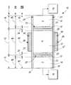
- a memory cell 10comprises a base region 12 between a pair of emitter/collector regions 14 and 16 .
- the regions 12 , 14 and 16may be comprised by a pillar-type structure in some embodiments, and such structure may be referred to as a BJT pillar.
- the emitter/collector region 14interfaces with the base region 12 at a junction 13 , and similarly the emitter/collector region 16 interfaces with the base region 12 at a junction 15 .
- one of the emitter/collector regionswill be the emitter region of the BJT device, and the other will be the collector region of the device.
- the junction between the base region and the emitter regionmay be referred to as a B-E junction, and the junction between the base region and the collector region may be referred to as a B-C junction.
- the emitter/collector regions 14 and 16are shown to be electrically coupled to electrical nodes 18 and 20 , respectively.
- One of the nodes 18 and 20may correspond to a bitline (i.e., a digit line or sense line).
- the other of the nodes 18 and 20may correspond to a wordline (i.e., an access line) in some embodiments, or to a ground or other electrically static structure in other embodiments.
- the illustrated BJT of memory cell 10has the base oppositely doped to the emitter/collector regions; and specifically comprises a p-type base and n-type emitter/collector regions.
- the base region and emitter/collector regionsmay comprise other doping arrangements, as illustrated in FIGS. 2-4 .
- the symbols “+” and “ ⁇ ”are utilized in FIG. 1 (and various other figures of this disclosure) to indicate dopant levels. Some or all of the designations p+, p, p ⁇ , n ⁇ , n and n+ may be used to indicate various levels and types of doping. The difference in dopant concentration between the regions identified as being p+, p, and p ⁇ may vary depending on the particular material being doped.
- An example dopant concentration of a p+ regionis a dopant concentration of at least about 10 19 atoms/cm 3 (and in some example applications may be from about 10 19 atoms/cm 3 to about 10 20 atoms/cm 3 ), an example dopant concentration of a p region is from about 10 18 to about 10 19 atoms/cm 3 , and an example dopant concentration of a p ⁇ region is less than about 5 ⁇ 10 18 atoms/cm 3 (and in some embodiments may be less than or equal to about 5 ⁇ 10 17 atoms/cm 3 ).
- the regions identified as being n ⁇ , n and n+may have dopant concentrations similar to those described above relative to the p ⁇ , p and p+ regions, respectively.
- p and ncan be utilized herein to refer to both dopant type and relative dopant concentrations.
- the terms “p” and “n”are to be understood as referring only to dopant type, and not to a relative dopant concentration, except when it is explicitly stated that the terms refer to relative dopant concentrations. Accordingly, for purposes of interpreting this disclosure and the claims that follow, it is to be understood that the terms “p-type doped” and n-type doped” refer to dopant types of a region and not to relative dopant levels.
- a p-type doped regioncan be doped to any of the p+, p, and p ⁇ dopant levels discussed above, and similarly an n-type doped region can be doped to any of the n+, n, and n ⁇ dopant levels discussed above.
- the dopants utilized in memory cell 10may be any suitable dopants.
- at least part of the memory cellwill comprise wide-bandgap material.
- An example wide-bandgap materialis silicon carbide, and such may be n-type doped with, for example, one or more of N (such as from N 2 and/or NH 3 ), P (such as from PH 3 ) and As (such as from AsH 3 ).
- the silicon carbidemay be p-type doped with, for example, one or more of B (such as from B 2 H 6 ), Al (such as from AlCl 3 , trimethylaluminum and triethylaluminum) and Ga (such as from trimethylgallium).
- depletion regions 22 and 24may be induced between base region 12 and the emitter/collector regions 14 and 16 , respectively.
- the depletion regionsare diagrammatically illustrated with cross-hatching. Approximate boundaries of the depletion region 22 are illustrated with dashed lines 23 , and approximate boundaries of the depletion region 24 are illustrated with dashed lines 25 .
- the memory cell 10has a gate 26 along the base region 12 .
- the base regionmay comprise an electrically floating body of the memory cell.
- the gatemay be used to enable charge to be selectively stored on such floating body, or to be drained from the floating body.
- the memory cellmay have two selectable memory states, with one of the states having more charge stored on base region 12 than the other state.
- the illustrated BJTis configured as a vertical pillar having a pair of opposing sidewalls 29 and 31 , and the gate 26 is shown to be bifurcated into a pair of segments 33 and 35 , with each segment being along one of the opposing sidewalls.
- the illustrated memory cellmay be one of a plurality of memory cells of a memory array
- the illustrated segments 33 and 35 of the gatemay correspond to a pair of lines that extend along multiple memory cells of a row or column of the array to interconnect multiple memory cells. Such lines would extend in and out of the page relative to the cross-sectional view of FIG. 1 .
- the segments 33 and 35may join with one another at some location outside of the view of FIG. 1 so that the illustrated segments 33 and 35 are actually two parts of the same gate.
- the gate 26comprises a material 27 .
- Such materialmay comprise any suitable substance, and may, for example, comprise one or more of various metals (for instance, titanium, tungsten, etc.), metal-containing compositions (for instance, metal silicide, metal nitride, etc.), and conductively-doped semiconductor materials (for instance, conductively-doped silicon, conducted-doped geranium, etc.).
- the gate 26is spaced from the sidewalls 29 and 31 of the BJT pillar by dielectric material 30 .
- the dielectric materialmay comprise any suitable composition or combination of compositions.
- at least a portion of the BJT pillarcomprises one or more forms of silicon carbide, and at least a portion of the dielectric material 30 that is directly against the silicon carbide comprises a passivation composition containing silicon, oxygen and nitrogen.
- Such passivation compositionmay be formed by chemically reacting a surface of the silicon carbide with oxygen and nitrogen, and/or by depositing a composition containing silicon, oxygen and nitrogen along the surface of the silicon carbide.
- an entirety of dielectric material 30may comprise the passivation composition containing silicon, oxygen and nitrogen.
- the dielectric material 30may comprise two or more different compositions, with the composition directly against surfaces of the BJT pillar being the passivation material, and with one or more other compositions being between the passivation material and the gate 26 .
- Such other compositionsmay comprise, for example, one or both of silicon dioxide and silicon nitride.
- the gate 26is along base region 12 of the BJT, but does not overlap the B-C and B-E junctions 13 and 15 . Further, the gate does not overlap the depletion regions 22 and 24 during operation of the BJT. In the shown configuration in which the BJT is within a vertical pillar, the gate 26 may be considered to vertically overlap the base region, and to not vertically overlap the depletion regions 22 and 24 .
- a gated BJT memory cellmay have primary leakage mechanisms that include gate-induced leakage (which may be referred to as gate-induced-drain-leakage, i.e., GIDL), base/emitter junction leakage, and base/collector junction leakage.
- gate-induced leakagewhich may be referred to as gate-induced-drain-leakage, i.e., GIDL
- base/emitter junction leakagei.e., GIDL
- base/collector junction leakagebase/collector junction leakage.
- the gatedoes not overlap the depletion regions, and thus only couples with the base region. Accordingly, the gate-induced leakage, if any, may be a small contribution to the overall leakage within the memory cell; and thus the overall leakage through the memory cell may be limited to the intrinsic leakage of the two junctions. This can enable the memory cell of FIG. 1 to have much longer retention times than conventional DRAM, and in some embodiments to have retention times suitable for utilization in nonvolatile memory.
- the BJT pillar of memory cell 10may be considered to be subdivided into numerous regions, as explained with reference to the scales I, II and III shown in FIG. 1 .
- Scale Iillustrates that the BJT pillar may be considered to comprise a first emitter/collector region 14 , a base region 12 , and a second emitter/collector region 16 .
- the regions 12 and 14interface at the junction 13
- the regions 12 and 16interface at the junction 15 .
- Scale IIillustrates that the BJT pillar may be considered to comprise a first outer region 40 corresponding to the portion of the emitter/collector region 14 that is outward of the depletion region 22 , a second outer region 42 corresponding to the portion of the emitter/collector region 16 that is outward of the depletion region 24 , and an inner region 44 between the outer regions 40 and 42 .
- the inner region 44interfaces with outer region 40 at an outermost edge of depletion region 22 , and interfaces with outer region 42 at an outermost edge of depletion region 24 .
- Scale IIIillustrates that the BJT pillar may be considered to comprise the outer regions 40 and 42 , the depletion regions 22 and 24 , and a neutral base region (or floating body region) 46 between the depletion regions.
- the BJT pillarmay comprise one or more wide-bandgap materials.
- the wide-bandgap materialsmay advantageously improve retention time of the memory cell relative to narrower-bandgap materials (such as silicon) by reducing leakage within the memory cell.
- wide-bandgap materialis provided at least across the junctions 13 and 15 in wide enough expanses to fully encompass depletion regions 22 and 24 .
- the wide-bandgap materialis provided across the locations where the wide-bandgap material may reduce base/collector junction leakage and base/emitter junction leakage.
- the wide-bandgap materialmay be provided as strips extending across depletion regions 22 and 24 , and thus the regions 40 , 46 and 42 of scale III may be narrow-bandgap materials (such as silicon).
- the wide-bandgap material across depletion region 22may be the same composition as the wide-bandgap material across depletion region 24 , or may be a different composition to tailor the BJT for a particular application of the memory cell 10 .
- Intrinsic leakagemay be considered to be derived through two different mechanisms, and to approximately correspond to whichever of the mechanisms predominates.
- One of the mechanismsis generation of intrinsic carriers in depletion regions, and the other is diffusion of intrinsic carriers in the neutral regions.
- concentration of intrinsic carriers (n i )may be represented by Equation I:
- n i⁇ ( - Eg 2 ⁇ ⁇ kT ) Equation ⁇ ⁇ I
- Equation IE g is the bandgap, T is temperature, and k is Boltzmann's constant.
- Intrinsic leakagewill be approximately proportional to n i for a leakage mechanism corresponding to generation of intrinsic carriers in depletion regions, and will be approximately proportional to (n i ) 2 (i.e., the squared concentration of intrinsic carriers) for a leakage mechanism corresponding to diffusion of intrinsic carriers in neutral regions.
- an increase in bandgapexponentially reduces n i , and thus exponentially reduces leakage.
- the leakage mechanism corresponding to diffusion of intrinsic carriers in neutral regionsis proportional to (n i ) 2
- the leakage mechanism corresponding to generation of intrinsic carriers in depletion regionsis proportional to n i
- the leakage mechanism corresponding to diffusion of intrinsic carriers in neutral regionsreduces very quickly with increasing bandgap so that the leakage mechanism corresponding to generation of intrinsic carriers in depletion regions is the predominant leakage mechanism for wide-bandgap materials.
- n iby about 10 orders of magnitude (i.e., 10 10 ) at 85° C.
- Retentionmay be directly proportional to leakage (all other things being equal), and thus a memory cell utilizing 3C-SiC may have 10 orders of magnitude better retention than an analogous memory cell utilizing silicon.
- a memory cell utilizing 3C-SiCmay have a retention time of at least about 10 years, or even at least about 20 years.
- the wide-bandgap materialsmay be provided anywhere in the BJT pillar where leakage may be problematic. For instance, it may be advantageous to provide wide-bandgap material across the region 40 of scale III when such region corresponds to an emitter region of the BJT (such as, for example, if the BJT is an npn BJT, the node 20 is a bitline, and the memory cell is operated in accordance with methodology described below with reference to FIGS. 5 and 6 ). In such embodiments, the wide-bandgap material across region 40 may be the same or different than the wide-bandgap material across one or both of the depletion regions 22 and 24 .
- wide-bandgap materialmay also be advantageous to provide wide-bandgap material within the regions 42 and 46 of scale III either to prevent leakage, or to simplify fabrication of memory cell 10 in embodiments in which wide-bandgap material as provided within depletion regions 22 and 24 .
- wide-bandgap materialis provided across all of the regions 40 , 22 , 46 , 24 and 42 of scale III.
- the same wide-bandgap materialmay be provided across all of the regions 40 , 22 , 46 , 24 and 42 so that the entirety of the vertical BJT pillar comprises, consists essentially of, or consists of only one wide-bandgap material.
- one or more of the regions 40 , 22 , 46 , 24 and 42may comprise a different wide-bandgap material than another region to tailor the memory cell 10 for a particular application.
- wide-bandgap materialmay be provided across region 44 of scale II to extend across the base region 12 and the depletion regions 22 and 24 .
- the wide-bandgap materialmay also extend across one or both of the regions 40 and 42 of the scale II.
- wide-bandgap materialextends across one or both of regions 40 and 42 , in addition to region 44 , the material may be the same across all of the regions 40 , 44 and 42 , or may differ in one or both of the regions 40 and 42 relative to region 44 to tailor the memory cell 10 for a particular application.
- the wide-bandgap materialmay comprise any suitable composition.
- the wide-bandgap materialmay comprise silicon and carbon, and may comprise one or more forms of silicon carbide.
- the wide-bandgap materialmay comprise, consist essentially of, or consist of the 3C form of silicon carbide in some embodiments, and thus may have a bandgap greater than 2.3 eV (specifically, such form of SiC has a bandgap of 2.36 eV).
- FIG. 2shows an example embodiment memory cell 10 a analogous to the memory cell 10 of FIG. 1 , but comprising a pnp BJT rather than an npn BJT.
- the memory cell 10 a of FIG. 2is labeled with identical numbering to that used above to describe FIG. 1 , and comprises identical features as the memory cell of FIG. 1 except for the different dopant type utilized in the base and emitter/collector regions.
- FIGS. 3 and 4show example embodiment memory cells 10 b and 10 c , respectively.
- the memory cells 10 b and 10 care analogous to the memory cell 10 of FIG. 1 , but comprise a same conductivity type throughout the base 12 and the emitter/collector regions 14 and 16 .
- the dopant level in the base regionis, however, less than the dopant levels in the base/collector regions.
- the memory cells 10 b and 10 c of FIGS. 3 and 4are labeled with identical numbering to that used above to describe FIG. 1 , and comprise identical features as the memory cell of FIG. 1 except for the dopant types utilized in the base and emitter/collector regions.
- the junctions 13 and 15 of FIGS. 3 and 4differ from those of FIG.
- the gates 26 of the memory cells 10 b and 10 cmay electrically induce a change in dopant type within the base regions coupled to such gates so that the BJTs of the memory cells function as npn and pnp BJTs, respectively, even though the BJTs are not initially doped as npn or pnp BJTs.
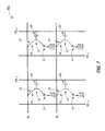
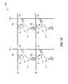
- FIG. 5diagrammatically illustrates a memory array 50 comprising a plurality of memory cells 10 of the type described above with reference to FIG. 1 .
- Each memory cellis schematically illustrated as a gated BJT, with the gate 26 illustrated to be capacitively coupled to the base 12 (the capacitive coupling is through the dielectric 30 , which is not shown in FIG. 5 ).
- the illustrated BJTs of FIG. 5have the region 14 as the emitter region and the region 16 as the collector region, but such orientation may be reversed in other embodiments.
- the memory array 50comprises a series of bitlines, a first series of wordlines (the series identified as WL 1 ), and a second series of wordlines (the series identified as WL 2 ).
- the node 20 of FIG. 1may correspond to a bitline (BL)
- the node 18 of FIG. 1may correspond to a wordline of the first series (WL 1 )
- the gate 26 of FIG. 1may be along a wordline of the second series (WL 2 ).
- the emitter/collector regions 16 of memory cells 10may be considered to be first emitter/collector regions which are directly coupled with bitlines, and the emitter/collector regions 14 of the memory cells may be considered to be second emitter/collector regions which are electrically coupled with the first series of wordlines.
- Each memory cell of array 50may be uniquely addressed through combinations containing one of the bitlines together with one of the wordlines WL 2 and/or one of the wordlines WL 1 .
- the wordlinesmay be alternatively referred to as access lines in some embodiments, and the bitlines may be alternatively referred to as sense lines in some embodiments.
- FIG. 6diagrammatically illustrates various operations that may be utilized for programming individual memory cells of the array 50 into a “0” data state (i.e., “write 0” operations), programming the individual memory cells into a “1” data state (i.e., “write 1” operations), and for reading the memory cells to ascertain the data states of the individual memory cells.
- FIG. 6also diagrammatically illustrates voltage of the P base (i.e., the base 12 of FIG. 1 ) during the various operations.
- Example voltage levels for the various states indicated in FIG. 6may include (assuming a bandgap of 2.3 eV):
- the terms “D0” and “D1”indicate voltages read for the “0” data state and the “1” data state, respectively, of the memory cell.
- the example operations of FIG. 6may advantageously achieve a high p-base programming margin (greater than or equal to about 1 V) between the D0 and D1 memory states of the memory cell, which may provide a sufficient charge to enable long retention by the memory cell, and to provide a margin against variation and disturb modes.
- the various voltages utilized for the reading and writing operationsmay be kept at relatively low levels (less than or equal to about 5 V) which may enable operation of the memory cell with modest power drain.
- Another set of example voltage levels for the various states indicated in FIG. 6may include (assuming a bandgap of 2.3 eV):
- the “write 0” operationhas a lower voltage differential between WL 1 and the bitline than does the “write 1” operation.
- the lower voltage differential between the bitline and WL 1allows charge to drain from the P base , while the higher voltage differential between the bitline and WL 1 results in charge being trapped on the P base .
- Various mechanismsmay account for such relationship. For instance, high-voltage differentials between the bitline and WL 1 during capacitive coupling of the base with gate 26 can lead to impact ionization, a Kirk effect, a Webster effect and/or other mechanisms which limit charge transfer through the BJT, and thus can lead to charge being trapped on the floating base of the BJT.
- low-voltage differentials between the bitline and WL 1 during the capacitive coupling of the gate with the basemay permit a steady flow of charge through the BJT, and thus may permit charge to be drained from the floating base.
- Equation II⁇ is the npn current gain.
- the impact ionization currentis equal to ⁇ n *I c , where ⁇ n is the impact ionization efficiency; and is a function of electric field divided by voltage. This leads to the relationship of Equation III.
- FIG. 7diagrammatically illustrates an example embodiment memory array 50 a comprising a plurality of memory cells 10 of the type described above with reference to FIG. 1 .
- the memory array of FIG. 7is similar to that of FIG. 5 , except that the first series of wordlines (WL 1 of FIG. 5 ) has been replaced with nodes 51 .
- the nodes 51are at a common voltage as one another, and in some embodiments may be electrically coupled with one another and with a common terminal (for instance, they may all be connected to a grounded plate).
- the node 20 of FIG. 1may correspond to the bitline (BL) of FIG. 7
- the node 18 of FIG. 1may correspond to a node 51
- the gate 26 of FIG. 1may be along a wordline of the series (WL 2 ).
- the emitter/collector regions 16 of memory cells 10may be considered to be first emitter/collector regions which are directly coupled with bitlines
- the emitter/collector regions 14 of the memory cellsmay be considered to be second emitter/collector regions which are electrically coupled with one another and with a common terminal.
- Each memory cell of array 50 amay be uniquely addressed through combinations containing one of the bitlines together with one of the wordlines WL 2 .
- FIG. 8diagrammatically illustrates various operations that may be utilized for programming individual memory cells of the array 50 a into a “0” data state (i.e., “write 0” operations), programming the individual memory cells into a “1” data state (i.e., “write 1” operations), and for reading the memory cells to ascertain the data states of the individual memory cells.
- FIG. 8also diagrammatically illustrates voltage of the P base (i.e., the base 12 of FIG. 1 ) during the various operations.
- Example voltage levels for the various states indicated in FIG. 8may include (assuming a bandgap of 2.3 eV, and assuming a common voltage on nodes 51 of 0V):
- FIG. 9diagrammatically illustrates another example embodiment memory array 50 b .
- the memory array of FIG. 9comprises a plurality of memory cells 10 a of the type described above with reference to FIG. 2 .
- the memory array of FIG. 9like that of FIG. 5 , comprises a series of bitlines, a first series of wordlines (the series identified as WL 1 ), and a second series of wordlines (the series identified as WL 2 ).
- the node 20 of FIG. 2may correspond to a bitline (BL)
- the node 18 of FIG. 2may correspond to a wordline of the first series (WL 1 )
- the gate 26 of FIG. 2may be along a wordline of the second series (WL 2 ).
- the emitter/collector regions 16 of memory cells 10 amay be considered to be first emitter/collector regions which are directly coupled with bitlines, and the emitter/collector regions 14 of the memory cells may be considered to be second emitter/collector region which are electrically coupled with the first series of wordlines.
- Each memory cell of array 50 bmay be uniquely addressed through combinations containing one of the bitlines together with one of the wordlines WL 2 and/or one of the wordlines WL 1 .
- FIG. 10diagrammatically illustrates various operations that may be utilized for programming individual memory cells of the array 50 b into a “0” data state (i.e., “write 0” operations), programming the individual memory cells into a “1” data state (i.e., “write 1” operations), and for reading the memory cells to ascertain the data states of the individual memory cells.
- FIG. 10also diagrammatically illustrates voltage of the N base (i.e., the base 12 of FIG. 2 ) during the various operations.
- Example voltage levels for the various states indicated in FIG. 10may include (assuming a bandgap of 2.3 eV):
- Another set of example voltage levels for the various states indicated in FIG. 10may include (assuming a bandgap of 2.3 eV):
- FIG. 11diagrammatically illustrates another set of operations that may be utilized for programming individual memory cells of the array 50 b of FIG. 9 into a “0” data state (i.e., “write 0” operations), programming the individual memory cells into a “1” data state (i.e., “write 1” operations), and for reading the memory cells to ascertain the data states of the individual memory cells.
- FIG. 11also diagrammatically illustrates voltage of the N base (i.e., the base 12 of FIG. 2 ) during the various operations.
- Example voltage levels for the various states indicated in FIG. 11may include (assuming a bandgap of 2.3 eV):
- Another set of example voltage levels for the various states indicated in FIG. 11may include (assuming a bandgap of 2.3 eV):
- FIG. 12diagrammatically illustrates an example embodiment memory array 50 c comprising a plurality of memory cells 10 a of the type described above with reference to FIG. 2 .
- the memory array of FIG. 12is similar to that of FIG. 9 , except that the first series of wordlines (WL 1 of FIG. 9 ) have been replaced with nodes 53 .
- the nodes 53are at a common voltage as one another, and in some embodiments may be electrically coupled with one another and with a common terminal (for instance, they may all be connected to an electrically conductive plate).
- the node 20 of FIG. 2may correspond to the bitline (BL) of FIG. 12
- the node 18 of FIG. 2may correspond to a node 53
- the gate 26 of FIG. 2may be along a wordline of the series (WL 2 ).
- the emitter/collector regions 16 of memory cells 10 amay be considered to be first emitter/collector regions which are directly coupled with bitlines
- the emitter/collector regions 14 of the memory cellsmay be considered to be second emitter/collector regions which are electrically coupled with one another and with a common terminal.
- Each memory cell of array 50 cmay be uniquely addressed through combinations containing one of the bitlines together with one of the wordlines WL 2 .
- FIG. 13diagrammatically illustrates various operations that may be utilized for programming individual memory cells of the array 50 c into a “0” data state (i.e., “write 0” operations), programming the individual memory cells into a “1” data state (i.e., “write 1” operations), and for reading the memory cells to ascertain the data states of the individual memory cells.
- FIG. 13also diagrammatically illustrates voltage of the N base (i.e., the base 12 of FIG. 2 ) during the various operations.
- Example voltage levels for the various states indicated in FIG. 13may include (assuming a bandgap of 2.3 eV, and assuming a common voltage on nodes 53 of 5V):
- FIG. 14diagrammatically illustrates another set of operations that may be utilized for programming individual memory cells of the array 50 c of FIG. 12 into a “0” data state (i.e., “write 0” operations), programming the individual memory cells into a “1” data state (i.e., “write 1” operations), and for reading the memory cells to ascertain the data states of the individual memory cells.
- FIG. 14also diagrammatically illustrates voltage of the N base (i.e., the base 12 of FIG. 2 ) during the various operations.
- Example voltage levels for the various states indicated in FIG. 14may include (assuming a bandgap of 2.3 eV, and assuming a common voltage on nodes 53 of 0V):
- FIGS. 15 and 16illustrate example semiconductor constructions comprising the memory cell 10 of FIG. 1 , and the memory cell 10 a of FIG. 2 , respectively.
- a semiconductor construction 60comprises memory cell 10 supported over a semiconductor substrate 62 .
- the substrate 62may comprise, consist essentially of, or consist of monocrystalline silicon in some embodiments, and is shown to be p-type background doped.
- semiconductor substratesemiconductor construction
- semiconductor substratemean any construction comprising semiconductive material, including, but not limited to, bulk semiconductive materials such as a semiconductive wafer (either alone or in assemblies comprising other materials), and semiconductive material layers (either alone or in assemblies comprising other materials).
- substraterefers to any supporting structure, including, but not limited to, the semiconductive substrates described above.
- substrate 62may comprise numerous materials in some embodiments.
- substrate 62may correspond to a semiconductor substrate containing one or more materials associated with integrated circuit fabrication.
- Example materials that may be associated with integrated circuit fabricationare various of refractory metal materials, barrier materials, diffusion materials, insulator materials, etc.
- the memory cell 10is part of a substantially vertical pillar 64 .
- Such pillarincludes an n-type doped segment 66 directly over the semiconductor material of substrate 62 (the segment 66 is shown doped to an n+ dopant level).
- segment 66may comprise monocrystalline silicon patterned from substrate 62 , and/or may comprise semiconductor material deposited over substrate 62 .
- the segment 66is shown electrically coupled with an electrically conductive material 68 that interconnects with node 18 .
- the conductive material 68may be any suitable material; including, for example, any of various metals, metal-containing compositions, and/or conductive-doped semiconductor materials.
- the conductive material 68may be a separate material from the conductively-doped material of segment 66 (as shown), or may be an extension of the conductively-doped material 66 .
- segment 66may be omitted and emitter/collector region 14 may directly contact a conductive node 18 comprising, consisting essentially of, or consisting of any of various metals and/or metal-containing compositions.
- the pillar 64is referred to as being “substantially vertical” to indicate that it extends substantially orthogonally to a primary upper surface of the substrate.
- verticalis used herein to define a relative orientation of an element or structure with respect to a major plane or surface of a wafer or substrate.
- a structuremay be referred to as being “substantially vertical” to indicate that the structure is vertical to within reasonable tolerances of fabrication and measurement.
- the pillar 64also includes an n-type doped segment 70 directly over the emitter/collector region 16 .
- the segment 70may comprise silicon and/or any other suitable semiconductor material.
- the segment 70is shown electrically coupled with an electrically conductive material 72 that interconnects with node 20 .
- the conductive material 72may be any suitable material; including, for example, any of various metals, metal-containing compositions, and/or conductive-doped semiconductor materials.
- the conductive material 72may be a separate material from the conductively-doped material of segment 70 (as shown), or may be an extension of the conductively-doped material 70 .
- segment 70may be omitted and emitter/collector region 16 may directly contact a conductive node 20 comprising, consisting essentially of, or consisting of any of various metals and/or metal-containing compositions.
- a semiconductor construction 60 acomprises memory cell 10 a supported over a semiconductor substrate 62 a .
- the substrate 62 amay comprise any of the compositions discussed above with reference to the substrate 62 of FIG. 15 .
- the memory cell 10 ais part of a substantially vertical pillar 64 a .
- Such pillarincludes a p-type doped segment 66 a directly over the semiconductor material of substrate 62 a .
- the segment 66 ais shown electrically coupled with an electrically conductive material 68 a that interconnects with node 18 .
- the conductive material 68 amay be any of the materials discussed above with reference to the material 68 of FIG. 15 .
- the conductive material 68 amay be a separate material from the conductively-doped material of segment 66 a (as shown), or may be an extension of the conductively-doped material 66 a .
- segment 66 amay be omitted and emitter/collector region 14 may directly contact a conductive node 18 comprising, consisting essentially of, or consisting of any of various metals and/or metal-containing compositions.
- the pillar 64 aalso includes a p-type doped segment 70 a directly over the emitter/collector region 16 .
- the segment 70 amay comprise silicon and/or any other suitable semiconductor material.
- the segment 70 ais shown electrically coupled with an electrically conductive material 72 a that interconnects with node 20 .
- the conductive material 72 amay comprise any of the materials discussed above with reference to the material 72 of FIG. 15 .
- the conductive material 72 amay be a separate material from the conductively-doped material of segment 70 a (as shown), or may be an extension of the conductively-doped material 70 a .
- segment 70 amay be omitted and emitter/collector region 16 may directly contact a conductive node 20 comprising, consisting essentially of, or consisting of any of various metals and/or metal-containing compositions.
- the memory cells having wide-bandgap materialmay be formed along one or more levels (or tiers) of an integrated circuit chip, and may be formed over one or more levels of logic or other circuitry fabricated by conventional methods (for instance, such other circuitry may comprise MOSFET transistors). Additionally, or alternatively, one or more levels of conventional circuitry may be fabricated over the memory cells containing the wide-bandgap material.
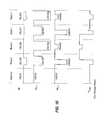
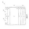
- FIGS. 17 and 18illustrate an example process for fabricating a memory array 50 a of the type shown in FIG. 7 comprising memory cells 10 of the type shown in FIG. 1 .
- a semiconductor construction 80comprises a substrate 82 having an n-type doped region 83 over a p-type doped region 81 .
- the substrate 82may be a semiconductor substrate analogous to the substrate 62 discussed above with reference to FIG. 15 .
- the regions 81 and 83may be conductively-doped regions of a monocrystalline silicon wafer, and/or may be conductively-doped regions formed along a tier of a partially-fabricated integrated circuit.
- Conductively-doped regions 12 , 14 and 16 of a memory cell stack 84are formed over substrate 82 .
- the entire stack 84may comprise, consist essentially of, or consist of doped wide-bandgap material (such as, for example, 3C-SiC). If doped region 83 comprises monocrystalline silicon and the wide-bandgap material comprises silicon carbide, the wide-bandgap material may be epitaxially grown over the monocrystalline silicon.
- a difficulty encountered in incorporating wide-bandgap materials (such as, for example, silicon carbide) into integrated circuit fabrication sequencesis that dopant activation within the wide-bandgap materials may utilize a thermal budget which is too high for many of the components conventionally utilized in integrated circuitry.
- a method of reducing the thermal budget for dopant activationis to in situ dope the wide-bandgap material during epitaxial growth of such material.
- a patterned mask 97is formed over memory cell stack 84 , with such patterned mask defining a pattern corresponding to a plurality of openings 99 that extend through the mask.
- the patterned maskmay comprise any suitable composition and may be formed with any suitable processing.
- the maskmay comprise photolithographically-patterned photoresist.
- the maskmay comprise one or more structures formed utilizing pitch multiplication methodologies.
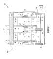
- a patternis transferred from mask 97 ( FIG. 17 ) into stack 84 with one or more suitable etches, and then the mask is removed.
- the memory cell stack 84is thus patterned into substantially vertical BJT pillars 88 .
- dielectric material 30is formed along sidewalls of the pillars.
- Electrically-conductive interconnects 90are formed between the pillars and in electrical connection with doped region 83 .
- the interconnects 90may be electrically coupled with one another through doped region 83 and/or through other interconnections, and may all be electrically connected to a common terminal so that they are all tied to the common voltage 51 (as shown).
- the dielectric material 30may be formed by initially providing surface passivation along outer exposed surfaces of pillars 88 .
- Such surface passivationmay comprise providing a layer containing silicon, oxygen and nitrogen along the outer surfaces.
- Such layermay be formed by nitridation/oxidation of exposed outer surfaces of silicon carbide in some embodiments, and/or by deposition of passivation material along the exposed outer surfaces.
- the dielectric material 30may consist of the passivation layer in some embodiments. In other embodiments, additional dielectric materials may be formed along the passivation layer to form a dielectric material 30 comprising the passivation layer in combination with other dielectric materials.
- Such other dielectric materialsmay comprise, for example, one or both of silicon dioxide and silicon nitride.
- material 90may comprise metal or other thermally-sensitive material, and an advantage of forming conductive material 90 after the doping of wide-bandgap material is that such can avoid exposure of the thermally-sensitive material to the thermal budget utilized for the doping of the wide-bandgap material.
- Electrically insulative material 92is formed over conductive material 90 and between the pillars 88 , and then the conductive material 27 is formed and patterned over insulative material 92 to form the gates 26 . Subsequently, another insulative material 94 is formed over gates 26 and insulative material 92 .
- the electrically insulative materials 92 and 94may comprise any suitable compositions or combinations of compositions, including for example, one or more of silicon dioxide, silicon nitride, and any of various doped oxide glasses (for instance, borophosphosilicate glass, phosphosilicate glass, fluorosilicate glass, etc.).
- the electrically insulative materials 92 and 94may be the same composition as one another in some embodiments, and may differ in composition from one another in other embodiments.
- bitline 100is formed across the pillars 88 , and in direct electrical contact with the upper doped regions 16 within such pillars.
- the bitline 100may be considered to be an example of a node 20 ( FIG. 1 ) that may be formed in direct electrical connection with the upper emitter/collector regions 16 of the illustrated example embodiment memory cells.
- Bitline 100may comprise any suitable electrically conductive material, and may, for example, comprise, consist essentially of, or consist of one or more of various metals, metal-containing compositions and conductively-doped semiconductor materials.
- bitlineis shown formed directly against the emitter/collector region 16 , in other embodiments there may be one or more electrically-conductive materials between the bitline and the emitter/collector region (such as, for example, an electrically conductive material analogous to the conductively-doped semiconductor material 70 of FIG. 15 ).
- the construction 80has a dimension from one side of a pillar to a same side of an adjacent pillar of 2F, and thus the individual memory cells may have footprints of about 4F 2 .
- FIGS. 17 and 18pertain to formation of memory cells 10 of the type shown in FIG. 1 in a memory array of the type shown in FIG. 7 , persons of ordinary skill will recognize that similar processing may be utilized to form any of the other memory cells described in this disclosure in any of the memory arrays described in this disclosure.
- the memory cells and memory arrays discussed abovemay be incorporated into integrated circuit chips or packages, and such may utilized in electronic devices and/or systems.
- the electronic systemsmay be used in, for example, memory modules, device drivers, power modules, communication modems, processor modules, and application-specific modules, and may include multilayer, multichip modules.
- the electronic systemsmay be any of a broad range of systems, such as, for example, clocks, televisions, cell phones, personal computers, automobiles, industrial control systems, aircraft, etc.
Landscapes
- Engineering & Computer Science (AREA)
- Physics & Mathematics (AREA)
- Condensed Matter Physics & Semiconductors (AREA)
- General Physics & Mathematics (AREA)
- Manufacturing & Machinery (AREA)
- Computer Hardware Design (AREA)
- Microelectronics & Electronic Packaging (AREA)
- Power Engineering (AREA)
- Chemical & Material Sciences (AREA)
- Materials Engineering (AREA)
- Semiconductor Memories (AREA)
- Metal-Oxide And Bipolar Metal-Oxide Semiconductor Integrated Circuits (AREA)
Abstract
Description
- Gated bipolar junction transistors, memory arrays, and methods of forming gated bipolar junction transistors.
- Memory is one type of integrated circuitry, and is used in computer systems for storing data. Integrated memory is usually fabricated in one or more arrays of individual memory cells. The memory cells might be volatile, semi-volatile, or nonvolatile. Nonvolatile memory cells can store data for extended periods of time, and in some instances can store data in the absence of power. Non-volatile memory is conventionally specified to be memory having a retention time of at least about 10 years. Volatile memory dissipates, and is therefore refreshed/rewritten to maintain data storage. Volatile memory may have a retention time of milliseconds, or less.
- The memory cells are configured to retain or store memory in at least two different selectable states. In a binary system, the states are considered as either a “0” or a “1”. In other systems, at least some individual memory cells may be configured to store more than two levels or states of information.
- Nonvolatile memory may be used in applications in which it is desired to retain data in the absence of power. Nonvolatile memory may also be used in applications in which power is a limited resource (such as in battery-operated devices) as an alternative to volatile memory because nonvolatile memory may have the advantage that it can conserve power relative to volatile memory. However, read/write characteristics of nonvolatile memory may be relatively slow in comparison to volatile memory, and/or nonvolatile memory may have limited endurance (for instance, nonvolatile memory may only function for about 105read/write cycles before failure). Thus, volatile memory is still often used, even in devices having limited reserves of power. It would be desirable to develop improved nonvolatile memory and/or improved semi-volatile memory. It would be further desirable to develop memory cells that are nonvolatile or semi-volatile, while having suitable read/write characteristics and endurance to replace conventional volatile memory in some applications.
- Integrated circuitry fabrication continues to strive to produce smaller and denser integrated circuits. It can be desired to develop small-footprint memory cells in order to conserve the valuable real estate of an integrated circuit chip. For instance, it can be desired to develop memory cells that have a footprint of less than or equal to 4F2, where “F” is the minimum dimension of masking features utilized to form the memory cells.
- It would be desirable to develop new memory cells which can be non-volatile or semi-volatile, and which have may have a footprint approaching 4F2.
FIG. 1 is a diagrammatic cross-sectional view of an example embodiment memory cell.FIG. 2 is a diagrammatic cross-sectional view of another example embodiment memory cell.FIG. 3 is a diagrammatic cross-sectional view of another example embodiment memory cell.FIG. 4 is a diagrammatic cross-sectional view of another example embodiment memory cell.FIG. 5 is a diagrammatic schematic view of an example embodiment memory array comprising memory cells of the type shown inFIG. 1 .FIG. 6 diagrammatically illustrates an example embodiment operational arrangement for utilizing the memory array ofFIG. 5 .FIG. 7 is a diagrammatic schematic view of another example embodiment memory array comprising memory cells of the type shown inFIG. 1 .FIG. 8 diagrammatically illustrates an example embodiment operational arrangement for utilizing the memory array ofFIG. 7 .FIG. 9 is a diagrammatic schematic view of an example embodiment memory array comprising memory cells of the type shown inFIG. 2 .FIGS. 10 and 11 diagrammatically illustrate example embodiment operational arrangements for utilizing the memory array ofFIG. 9 .FIG. 12 is a diagrammatic schematic view of another example embodiment memory array comprising memory cells of the type shown inFIG. 2 .FIGS. 13 and 14 diagrammatically illustrate example embodiment operational arrangements for utilizing the memory array ofFIG. 12 .FIG. 15 is a diagrammatic cross-sectional view of another example embodiment memory cell.FIG. 16 is a diagrammatic cross-sectional view of another example embodiment memory cell.FIGS. 17 and 18 diagrammatically illustrate process stages of an example embodiment method for fabricating an array of memory cells.- Some embodiments include memory cells comprising one or more wide-bandgap materials; with a “wide-bandgap material” being a material having a bandgap measurably greater than the 1.12 eV bandgap of silicon. In some embodiments, the wide-bandgap material may have a bandgap of 1.2 eV or greater. In some embodiments, the wide-bandgap material may have a bandgap of 2.3 eV or greater, and may, for example, comprise one or more forms of silicon carbide.
- The memory cells may be gated bipolar junction transistors (BJTs), and may comprise electrically floating bodies. In some embodiments, the wide-bandgap material may be utilized in the floating bodies and/or in depletion regions adjacent the floating bodies. Such utilization of the wide-bandgap material may enable formation of random access memory (RAM) having longer retention time than conventional dynamic random access memory (DRAM), while also having suitably fast read/write characteristics to substitute for conventional DRAM in some applications. Additionally, or alternatively, the wide-bandgap material may enable formation of memory having retention times of several years, and thus may enable formation of nonvolatile memory. In some embodiments, the nonvolatile memory may have endurance approaching, or even exceeding, the endurance of conventional DRAM (such as endurance suitable to survive 106or more read/write cycles).
- Example gated BJT memory cells are described with reference to
FIGS. 1-4 . - Referring to
FIG. 1 , amemory cell 10 comprises abase region 12 between a pair of emitter/collector regions regions - The emitter/
collector region 14 interfaces with thebase region 12 at ajunction 13, and similarly the emitter/collector region 16 interfaces with thebase region 12 at ajunction 15. In operation, one of the emitter/collector regions will be the emitter region of the BJT device, and the other will be the collector region of the device. The junction between the base region and the emitter region may be referred to as a B-E junction, and the junction between the base region and the collector region may be referred to as a B-C junction. - The emitter/
collector regions electrical nodes nodes nodes - The illustrated BJT of
memory cell 10 has the base oppositely doped to the emitter/collector regions; and specifically comprises a p-type base and n-type emitter/collector regions. In other embodiments, the base region and emitter/collector regions may comprise other doping arrangements, as illustrated inFIGS. 2-4 . - The symbols “+” and “−” are utilized in
FIG. 1 (and various other figures of this disclosure) to indicate dopant levels. Some or all of the designations p+, p, p−, n−, n and n+ may be used to indicate various levels and types of doping. The difference in dopant concentration between the regions identified as being p+, p, and p− may vary depending on the particular material being doped. An example dopant concentration of a p+ region is a dopant concentration of at least about 1019atoms/cm3(and in some example applications may be from about 1019atoms/cm3to about 1020atoms/cm3), an example dopant concentration of a p region is from about 1018to about 1019atoms/cm3, and an example dopant concentration of a p− region is less than about 5×10¹⁸atoms/cm3(and in some embodiments may be less than or equal to about 5×10¹⁷atoms/cm3). The regions identified as being n−, n and n+ may have dopant concentrations similar to those described above relative to the p−, p and p+ regions, respectively. - It is noted that the terms “p” and “n” can be utilized herein to refer to both dopant type and relative dopant concentrations. The terms “p” and “n” are to be understood as referring only to dopant type, and not to a relative dopant concentration, except when it is explicitly stated that the terms refer to relative dopant concentrations. Accordingly, for purposes of interpreting this disclosure and the claims that follow, it is to be understood that the terms “p-type doped” and n-type doped” refer to dopant types of a region and not to relative dopant levels. Thus, a p-type doped region can be doped to any of the p+, p, and p− dopant levels discussed above, and similarly an n-type doped region can be doped to any of the n+, n, and n− dopant levels discussed above.
- The dopants utilized in
memory cell 10 may be any suitable dopants. In some embodiments, at least part of the memory cell will comprise wide-bandgap material. An example wide-bandgap material is silicon carbide, and such may be n-type doped with, for example, one or more of N (such as from N2and/or NH3), P (such as from PH3) and As (such as from AsH3). Alternatively, the silicon carbide may be p-type doped with, for example, one or more of B (such as from B2H6), Al (such as from AlCl3, trimethylaluminum and triethylaluminum) and Ga (such as from trimethylgallium). - In operation,
depletion regions base region 12 and the emitter/collector regions depletion region 22 are illustrated with dashedlines 23, and approximate boundaries of thedepletion region 24 are illustrated with dashedlines 25. - The
memory cell 10 has agate 26 along thebase region 12. In operation, the base region may comprise an electrically floating body of the memory cell. The gate may be used to enable charge to be selectively stored on such floating body, or to be drained from the floating body. Thus, the memory cell may have two selectable memory states, with one of the states having more charge stored onbase region 12 than the other state. - The illustrated BJT is configured as a vertical pillar having a pair of opposing
sidewalls gate 26 is shown to be bifurcated into a pair ofsegments segments FIG. 1 . Thesegments FIG. 1 so that the illustratedsegments - The
gate 26 comprises amaterial 27. Such material may comprise any suitable substance, and may, for example, comprise one or more of various metals (for instance, titanium, tungsten, etc.), metal-containing compositions (for instance, metal silicide, metal nitride, etc.), and conductively-doped semiconductor materials (for instance, conductively-doped silicon, conducted-doped geranium, etc.). - The
gate 26 is spaced from thesidewalls dielectric material 30. The dielectric material may comprise any suitable composition or combination of compositions. In some embodiments, at least a portion of the BJT pillar comprises one or more forms of silicon carbide, and at least a portion of thedielectric material 30 that is directly against the silicon carbide comprises a passivation composition containing silicon, oxygen and nitrogen. Such passivation composition may be formed by chemically reacting a surface of the silicon carbide with oxygen and nitrogen, and/or by depositing a composition containing silicon, oxygen and nitrogen along the surface of the silicon carbide. - In some embodiments, an entirety of
dielectric material 30 may comprise the passivation composition containing silicon, oxygen and nitrogen. In other embodiments, thedielectric material 30 may comprise two or more different compositions, with the composition directly against surfaces of the BJT pillar being the passivation material, and with one or more other compositions being between the passivation material and thegate 26. Such other compositions may comprise, for example, one or both of silicon dioxide and silicon nitride. - In the shown embodiment, the
gate 26 is alongbase region 12 of the BJT, but does not overlap the B-C andB-E junctions depletion regions gate 26 may be considered to vertically overlap the base region, and to not vertically overlap thedepletion regions - It can be advantageous for
gate 26 to not overlapdepletion regions gate 26 overlaps the depletion regions, then a significant leakage mechanism within the memory cell may be gate-induced leakage, and such may be a much larger contribution to the leakage within the memory cell than the combination of intrinsic base/emitter junction leakage and intrinsic base/collector junction leakage. In the shown example embodiment ofFIG. 1 , the gate does not overlap the depletion regions, and thus only couples with the base region. Accordingly, the gate-induced leakage, if any, may be a small contribution to the overall leakage within the memory cell; and thus the overall leakage through the memory cell may be limited to the intrinsic leakage of the two junctions. This can enable the memory cell ofFIG. 1 to have much longer retention times than conventional DRAM, and in some embodiments to have retention times suitable for utilization in nonvolatile memory. - The BJT pillar of
memory cell 10 may be considered to be subdivided into numerous regions, as explained with reference to the scales I, II and III shown inFIG. 1 . - Scale I illustrates that the BJT pillar may be considered to comprise a first emitter/
collector region 14, abase region 12, and a second emitter/collector region 16. Theregions junction 13, and theregions junction 15. - Scale II illustrates that the BJT pillar may be considered to comprise a first
outer region 40 corresponding to the portion of the emitter/collector region 14 that is outward of thedepletion region 22, a secondouter region 42 corresponding to the portion of the emitter/collector region 16 that is outward of thedepletion region 24, and aninner region 44 between theouter regions inner region 44 interfaces withouter region 40 at an outermost edge ofdepletion region 22, and interfaces withouter region 42 at an outermost edge ofdepletion region 24. - Scale III illustrates that the BJT pillar may be considered to comprise the
outer regions depletion regions - As discussed above, the BJT pillar may comprise one or more wide-bandgap materials. The wide-bandgap materials may advantageously improve retention time of the memory cell relative to narrower-bandgap materials (such as silicon) by reducing leakage within the memory cell. In some embodiments, wide-bandgap material is provided at least across the
junctions depletion regions depletion regions regions depletion region 22 may be the same composition as the wide-bandgap material acrossdepletion region 24, or may be a different composition to tailor the BJT for a particular application of thememory cell 10. - Possible means by which the wide bandgap materials may reduce leakage within the BJT are as follows. Intrinsic leakage may be considered to be derived through two different mechanisms, and to approximately correspond to whichever of the mechanisms predominates. One of the mechanisms is generation of intrinsic carriers in depletion regions, and the other is diffusion of intrinsic carriers in the neutral regions. The concentration of intrinsic carriers (ni) may be represented by Equation I:
- In Equation I, Egis the bandgap, T is temperature, and k is Boltzmann's constant. Intrinsic leakage will be approximately proportional to nifor a leakage mechanism corresponding to generation of intrinsic carriers in depletion regions, and will be approximately proportional to (ni)2(i.e., the squared concentration of intrinsic carriers) for a leakage mechanism corresponding to diffusion of intrinsic carriers in neutral regions. In either event, an increase in bandgap exponentially reduces ni, and thus exponentially reduces leakage. Further, since the leakage mechanism corresponding to diffusion of intrinsic carriers in neutral regions is proportional to (ni)2, while the leakage mechanism corresponding to generation of intrinsic carriers in depletion regions is proportional to ni, the leakage mechanism corresponding to diffusion of intrinsic carriers in neutral regions reduces very quickly with increasing bandgap so that the leakage mechanism corresponding to generation of intrinsic carriers in depletion regions is the predominant leakage mechanism for wide-bandgap materials.
- The reduction in leakage obtained utilizing wide-bandgap materials may be enormous. For instance, substitution of 3C-SiC (bandgap 2.52 eV) for silicon (bandgap 1.12 eV) may decrease niby about 10 orders of magnitude (i.e., 1010) at 85° C. Retention may be directly proportional to leakage (all other things being equal), and thus a memory cell utilizing 3C-SiC may have 10 orders of magnitude better retention than an analogous memory cell utilizing silicon. In some embodiments, a memory cell utilizing 3C-SiC may have a retention time of at least about 10 years, or even at least about 20 years.
- The wide-bandgap materials may be provided anywhere in the BJT pillar where leakage may be problematic. For instance, it may be advantageous to provide wide-bandgap material across the
region 40 of scale III when such region corresponds to an emitter region of the BJT (such as, for example, if the BJT is an npn BJT, thenode 20 is a bitline, and the memory cell is operated in accordance with methodology described below with reference toFIGS. 5 and 6 ). In such embodiments, the wide-bandgap material acrossregion 40 may be the same or different than the wide-bandgap material across one or both of thedepletion regions regions memory cell 10 in embodiments in which wide-bandgap material as provided withindepletion regions regions regions regions memory cell 10 for a particular application. - In some embodiments, wide-bandgap material may be provided across
region 44 of scale II to extend across thebase region 12 and thedepletion regions regions region 40 ifregion 40 is an emitter region of the BJT. Further, it may be advantageous for the wide-bandgap material to extend acrossregion 42, either to alleviate a leakage mechanism, or to simplify fabrication of the memory cell having the wide-bandgap material inregion 44. If wide-bandgap material extends across one or both ofregions region 44, the material may be the same across all of theregions regions region 44 to tailor thememory cell 10 for a particular application. - The wide-bandgap material may comprise any suitable composition. In some embodiments, the wide-bandgap material may comprise silicon and carbon, and may comprise one or more forms of silicon carbide. For instance, the wide-bandgap material may comprise, consist essentially of, or consist of the 3C form of silicon carbide in some embodiments, and thus may have a bandgap greater than 2.3 eV (specifically, such form of SiC has a bandgap of 2.36 eV).
FIG. 2 shows an exampleembodiment memory cell 10aanalogous to thememory cell 10 ofFIG. 1 , but comprising a pnp BJT rather than an npn BJT. Thememory cell 10aofFIG. 2 is labeled with identical numbering to that used above to describeFIG. 1 , and comprises identical features as the memory cell ofFIG. 1 except for the different dopant type utilized in the base and emitter/collector regions.FIGS. 3 and 4 show exampleembodiment memory cells memory cells memory cell 10 ofFIG. 1 , but comprise a same conductivity type throughout thebase 12 and the emitter/collector regions memory cells FIGS. 3 and 4 are labeled with identical numbering to that used above to describeFIG. 1 , and comprise identical features as the memory cell ofFIG. 1 except for the dopant types utilized in the base and emitter/collector regions. Thejunctions FIGS. 3 and 4 differ from those ofFIG. 1 in that they are interfaces where different dopant levels meet, rather than being interfaces where different dopant types meet. In operation, thegates 26 of thememory cells - The memory cells of
FIGS. 1-4 may be utilized in memory arrays.FIG. 5 diagrammatically illustrates amemory array 50 comprising a plurality ofmemory cells 10 of the type described above with reference toFIG. 1 . Each memory cell is schematically illustrated as a gated BJT, with thegate 26 illustrated to be capacitively coupled to the base12 (the capacitive coupling is through the dielectric30, which is not shown inFIG. 5 ). The illustrated BJTs ofFIG. 5 have theregion 14 as the emitter region and theregion 16 as the collector region, but such orientation may be reversed in other embodiments. - The
memory array 50 comprises a series of bitlines, a first series of wordlines (the series identified as WL1), and a second series of wordlines (the series identified as WL2). In some embodiments, thenode 20 ofFIG. 1 may correspond to a bitline (BL), thenode 18 ofFIG. 1 may correspond to a wordline of the first series (WL1), and thegate 26 ofFIG. 1 may be along a wordline of the second series (WL2). In such embodiments, the emitter/collector regions 16 ofmemory cells 10 may be considered to be first emitter/collector regions which are directly coupled with bitlines, and the emitter/collector regions 14 of the memory cells may be considered to be second emitter/collector regions which are electrically coupled with the first series of wordlines. Each memory cell ofarray 50 may be uniquely addressed through combinations containing one of the bitlines together with one of the wordlines WL2and/or one of the wordlines WL1. The wordlines may be alternatively referred to as access lines in some embodiments, and the bitlines may be alternatively referred to as sense lines in some embodiments. FIG. 6 diagrammatically illustrates various operations that may be utilized for programming individual memory cells of thearray 50 into a “0” data state (i.e., “write 0” operations), programming the individual memory cells into a “1” data state (i.e., “write 1” operations), and for reading the memory cells to ascertain the data states of the individual memory cells.FIG. 6 also diagrammatically illustrates voltage of the Pbase(i.e., thebase 12 ofFIG. 1 ) during the various operations. Example voltage levels for the various states indicated inFIG. 6 may include (assuming a bandgap of 2.3 eV):- VBLID=0 Volt (V)
- VBLW0=2V
- VBLRD=0V (D0, 0V; D1, 1V)
- VBLW1=0V
- VW1ID=0V
- VW1WT=3V
- VW1RD=5V
- VW2ID=−3V
- VW2WT=2V
- VW2RD=−2V
- The terms “D0” and “D1” indicate voltages read for the “0” data state and the “1” data state, respectively, of the memory cell. The example operations of
FIG. 6 may advantageously achieve a high p-base programming margin (greater than or equal to about 1 V) between the D0 and D1 memory states of the memory cell, which may provide a sufficient charge to enable long retention by the memory cell, and to provide a margin against variation and disturb modes. Also, the various voltages utilized for the reading and writing operations may be kept at relatively low levels (less than or equal to about 5 V) which may enable operation of the memory cell with modest power drain. - Another set of example voltage levels for the various states indicated in
FIG. 6 may include (assuming a bandgap of 2.3 eV): - VBLID=0V
- VBLW0=3V
- VBLRD=0V (D0, 0V; D1, 1V)
- VBLW1=0V
- VW1ID=0V
- VW1WT=5V
- VW1RD=5V
- VW2ID=−3V
- VW2WT=2V
- VW2RD=−2V
- It is noted that the “
write 0” operation has a lower voltage differential between WL1and the bitline than does the “write 1” operation. The lower voltage differential between the bitline and WL1allows charge to drain from the Pbase, while the higher voltage differential between the bitline and WL1results in charge being trapped on the Pbase. Various mechanisms may account for such relationship. For instance, high-voltage differentials between the bitline and WL1during capacitive coupling of the base withgate 26 can lead to impact ionization, a Kirk effect, a Webster effect and/or other mechanisms which limit charge transfer through the BJT, and thus can lead to charge being trapped on the floating base of the BJT. In contrast, low-voltage differentials between the bitline and WL1during the capacitive coupling of the gate with the base may permit a steady flow of charge through the BJT, and thus may permit charge to be drained from the floating base. - A possible explanation for the reason that the lower voltage differential between the bitline and WL1allows charge to drain from the Pbase, while the higher voltage differential between the bitline and WL1results in charge being trapped on the Pbaseis as follows. When the voltage differential is high, there is impact ionization in the collector-base region. This supplies a base current (Ib) to the npn bipolar transistor. A collector current (Ic) results, which is related to the base current through Equation II.
Ici =β*Ib Equation II- In Equation II, β is the npn current gain.
- The impact ionization current is equal to αn*Ic, where αnis the impact ionization efficiency; and is a function of electric field divided by voltage. This leads to the relationship of Equation III.
Ib=αn*Ic Equation III- If (αn*β)>1, the cell latches. Once the cell latches, the gate (26 of
FIG. 5 ) losses control of the Pbaseand cannot couple to it. Hence, even if the gate voltage is brought down, the Pbasevoltage stays high. In contrast, with a low voltage differential the cell does not latch, the gate has good coupling to the Pbase, and pulling the gate voltage down will also pull the Pbasevoltage down. FIG. 7 diagrammatically illustrates an exampleembodiment memory array 50acomprising a plurality ofmemory cells 10 of the type described above with reference toFIG. 1 . The memory array ofFIG. 7 is similar to that ofFIG. 5 , except that the first series of wordlines (WL1ofFIG. 5 ) has been replaced withnodes 51. Thenodes 51 are at a common voltage as one another, and in some embodiments may be electrically coupled with one another and with a common terminal (for instance, they may all be connected to a grounded plate).- In some embodiments, the
node 20 ofFIG. 1 may correspond to the bitline (BL) ofFIG. 7 , thenode 18 ofFIG. 1 may correspond to anode 51, and thegate 26 ofFIG. 1 may be along a wordline of the series (WL2). In such embodiments, the emitter/collector regions 16 ofmemory cells 10 may be considered to be first emitter/collector regions which are directly coupled with bitlines, and the emitter/collector regions 14 of the memory cells may be considered to be second emitter/collector regions which are electrically coupled with one another and with a common terminal. Each memory cell ofarray 50amay be uniquely addressed through combinations containing one of the bitlines together with one of the wordlines WL2. FIG. 8 diagrammatically illustrates various operations that may be utilized for programming individual memory cells of thearray 50ainto a “0” data state (i.e., “write 0” operations), programming the individual memory cells into a “1” data state (i.e., “write 1” operations), and for reading the memory cells to ascertain the data states of the individual memory cells.FIG. 8 also diagrammatically illustrates voltage of the Pbase(i.e., thebase 12 ofFIG. 1 ) during the various operations. Example voltage levels for the various states indicated inFIG. 8 may include (assuming a bandgap of 2.3 eV, and assuming a common voltage onnodes 51 of 0V):- VBLID=2V
- VBLW0=2V
- VBLRD=5V (D0, 5V; D1, 4V)
- VBLW1=4V
- VW2ID=−3V
- VW2WT=2V
- VW2RD=−1.4V
FIG. 9 diagrammatically illustrates another exampleembodiment memory array 50b. The memory array ofFIG. 9 comprises a plurality ofmemory cells 10aof the type described above with reference toFIG. 2 . The memory array ofFIG. 9 , like that ofFIG. 5 , comprises a series of bitlines, a first series of wordlines (the series identified as WL1), and a second series of wordlines (the series identified as WL2). In some embodiments, thenode 20 ofFIG. 2 may correspond to a bitline (BL), thenode 18 ofFIG. 2 may correspond to a wordline of the first series (WL1), and thegate 26 ofFIG. 2 may be along a wordline of the second series (WL2). In such embodiments, the emitter/collector regions 16 ofmemory cells 10amay be considered to be first emitter/collector regions which are directly coupled with bitlines, and the emitter/collector regions 14 of the memory cells may be considered to be second emitter/collector region which are electrically coupled with the first series of wordlines. Each memory cell ofarray 50bmay be uniquely addressed through combinations containing one of the bitlines together with one of the wordlines WL2and/or one of the wordlines WL1.FIG. 10 diagrammatically illustrates various operations that may be utilized for programming individual memory cells of thearray 50binto a “0” data state (i.e., “write 0” operations), programming the individual memory cells into a “1” data state (i.e., “write 1” operations), and for reading the memory cells to ascertain the data states of the individual memory cells.FIG. 10 also diagrammatically illustrates voltage of the Nbase(i.e., thebase 12 ofFIG. 2 ) during the various operations. Example voltage levels for the various states indicated inFIG. 10 may include (assuming a bandgap of 2.3 eV):- VBLID=5V
- VBLW0=4V
- VBLRD=5V (D0, 5V; D1, 4V)
- VBLW1=5V
- VW1ID=5V
- VW1WT=1V
- VW1RD=0V
- VW2ID=5V
- VW2WT=0V
- VW2RD=4V
- Another set of example voltage levels for the various states indicated in
FIG. 10 may include (assuming a bandgap of 2.3 eV): - VBLID=5V
- VBLW0=3V
- VBLRD=5V (D0, 5V; D1, 4V)
- VBLW1=5V
- VW1ID=5V
- VW1WT=0V
- VW1RD=0V
- VW2ID=5V
- VW2WT=0V
- VW2RD=4V
FIG. 11 diagrammatically illustrates another set of operations that may be utilized for programming individual memory cells of thearray 50bofFIG. 9 into a “0” data state (i.e., “write 0” operations), programming the individual memory cells into a “1” data state (i.e., “write 1” operations), and for reading the memory cells to ascertain the data states of the individual memory cells.FIG. 11 also diagrammatically illustrates voltage of the Nbase(i.e., thebase 12 ofFIG. 2 ) during the various operations. Example voltage levels for the various states indicated inFIG. 11 may include (assuming a bandgap of 2.3 eV):- VBLID=0V
- VBLW0=2V
- VBLRD=0V (D0, 0V; D1, 1V)
- VBLW1=0V
- VW1ID=0V
- VW1 WT=4V
- VW1RD=5V
- VW2ID=5V
- VW2WT=0V
- VW2RD=4V
- Another set of example voltage levels for the various states indicated in
FIG. 11 may include (assuming a bandgap of 2.3 eV): - VBLID=0V
- VBLW0=3V
- VBLRD=0V (D0, 0V; D1, 1V)
- VBLW1=0V
- VW1ID=0V
- VW1WT=5V
- VW1RD=5V
- VW2ID=5V
- VW2WT=0V
- VW2RD=4V
FIG. 12 diagrammatically illustrates an exampleembodiment memory array 50ccomprising a plurality ofmemory cells 10aof the type described above with reference toFIG. 2 . The memory array ofFIG. 12 is similar to that ofFIG. 9 , except that the first series of wordlines (WL1ofFIG. 9 ) have been replaced withnodes 53. Thenodes 53 are at a common voltage as one another, and in some embodiments may be electrically coupled with one another and with a common terminal (for instance, they may all be connected to an electrically conductive plate).- In some embodiments, the
node 20 ofFIG. 2 may correspond to the bitline (BL) ofFIG. 12 , thenode 18 ofFIG. 2 may correspond to anode 53, and thegate 26 ofFIG. 2 may be along a wordline of the series (WL2). In such embodiments, the emitter/collector regions 16 ofmemory cells 10amay be considered to be first emitter/collector regions which are directly coupled with bitlines, and the emitter/collector regions 14 of the memory cells may be considered to be second emitter/collector regions which are electrically coupled with one another and with a common terminal. Each memory cell ofarray 50cmay be uniquely addressed through combinations containing one of the bitlines together with one of the wordlines WL2. FIG. 13 diagrammatically illustrates various operations that may be utilized for programming individual memory cells of thearray 50cinto a “0” data state (i.e., “write 0” operations), programming the individual memory cells into a “1” data state (i.e., “write 1” operations), and for reading the memory cells to ascertain the data states of the individual memory cells.FIG. 13 also diagrammatically illustrates voltage of the Nbase(i.e., thebase 12 ofFIG. 2 ) during the various operations. Example voltage levels for the various states indicated inFIG. 13 may include (assuming a bandgap of 2.3 eV, and assuming a common voltage onnodes 53 of 5V):- VBLID=3V
- VBLW0=3V
- VBLRD=0V (D0, 0V; D1, 1V)
- VBLW1=0V
- VW2ID=5V
- VW2WT=0V
- VW2RD=3.4V
FIG. 14 diagrammatically illustrates another set of operations that may be utilized for programming individual memory cells of thearray 50cofFIG. 12 into a “0” data state (i.e., “write 0” operations), programming the individual memory cells into a “1” data state (i.e., “write 1” operations), and for reading the memory cells to ascertain the data states of the individual memory cells.FIG. 14 also diagrammatically illustrates voltage of the Nbase(i.e., thebase 12 ofFIG. 2 ) during the various operations. Example voltage levels for the various states indicated inFIG. 14 may include (assuming a bandgap of 2.3 eV, and assuming a common voltage onnodes 53 of 0V):- VBLID=2V
- VBLW0=2V
- VBLRD=5V (D0, 5V; D1, 4V)
- VBLW1=4V
- VW2ID=5V
- VW2WT=0V
- VW2RD=3.4V
- The memory cells of
FIGS. 1-4 may be readily incorporated into semiconductor constructions.FIGS. 15 and 16 illustrate example semiconductor constructions comprising thememory cell 10 ofFIG. 1 , and thememory cell 10aofFIG. 2 , respectively. - Referring to
FIG. 15 , asemiconductor construction 60 comprisesmemory cell 10 supported over asemiconductor substrate 62. Thesubstrate 62 may comprise, consist essentially of, or consist of monocrystalline silicon in some embodiments, and is shown to be p-type background doped. The terms “semiconductive substrate,” “semiconductor construction” and “semiconductor substrate” mean any construction comprising semiconductive material, including, but not limited to, bulk semiconductive materials such as a semiconductive wafer (either alone or in assemblies comprising other materials), and semiconductive material layers (either alone or in assemblies comprising other materials). The term “substrate” refers to any supporting structure, including, but not limited to, the semiconductive substrates described above. Althoughsubstrate 62 is shown to be homogenous, the substrate may comprise numerous materials in some embodiments. For instance,substrate 62 may correspond to a semiconductor substrate containing one or more materials associated with integrated circuit fabrication. Example materials that may be associated with integrated circuit fabrication are various of refractory metal materials, barrier materials, diffusion materials, insulator materials, etc. - The
memory cell 10 is part of a substantiallyvertical pillar 64. Such pillar includes an n-type dopedsegment 66 directly over the semiconductor material of substrate62 (thesegment 66 is shown doped to an n+ dopant level). In some embodiments,segment 66 may comprise monocrystalline silicon patterned fromsubstrate 62, and/or may comprise semiconductor material deposited oversubstrate 62. Thesegment 66 is shown electrically coupled with an electricallyconductive material 68 that interconnects withnode 18. Theconductive material 68 may be any suitable material; including, for example, any of various metals, metal-containing compositions, and/or conductive-doped semiconductor materials. Theconductive material 68 may be a separate material from the conductively-doped material of segment66 (as shown), or may be an extension of the conductively-dopedmaterial 66. In some embodiments,segment 66 may be omitted and emitter/collector region 14 may directly contact aconductive node 18 comprising, consisting essentially of, or consisting of any of various metals and/or metal-containing compositions. - The
pillar 64 is referred to as being “substantially vertical” to indicate that it extends substantially orthogonally to a primary upper surface of the substrate. Specifically, the term “vertical” is used herein to define a relative orientation of an element or structure with respect to a major plane or surface of a wafer or substrate. A structure may be referred to as being “substantially vertical” to indicate that the structure is vertical to within reasonable tolerances of fabrication and measurement. - The
pillar 64 also includes an n-type dopedsegment 70 directly over the emitter/collector region 16. Thesegment 70 may comprise silicon and/or any other suitable semiconductor material. Thesegment 70 is shown electrically coupled with an electrically conductive material72 that interconnects withnode 20. The conductive material72 may be any suitable material; including, for example, any of various metals, metal-containing compositions, and/or conductive-doped semiconductor materials. The conductive material72 may be a separate material from the conductively-doped material of segment70 (as shown), or may be an extension of the conductively-dopedmaterial 70. In some embodiments,segment 70 may be omitted and emitter/collector region 16 may directly contact aconductive node 20 comprising, consisting essentially of, or consisting of any of various metals and/or metal-containing compositions. - Referring to
FIG. 16 , asemiconductor construction 60acomprisesmemory cell 10asupported over asemiconductor substrate 62a. Thesubstrate 62amay comprise any of the compositions discussed above with reference to thesubstrate 62 ofFIG. 15 . - The
memory cell 10ais part of a substantiallyvertical pillar 64a. Such pillar includes a p-type dopedsegment 66adirectly over the semiconductor material ofsubstrate 62a. Thesegment 66ais shown electrically coupled with an electricallyconductive material 68athat interconnects withnode 18. Theconductive material 68amay be any of the materials discussed above with reference to thematerial 68 ofFIG. 15 . Theconductive material 68amay be a separate material from the conductively-doped material ofsegment 66a(as shown), or may be an extension of the conductively-dopedmaterial 66a. In some embodiments,segment 66amay be omitted and emitter/collector region 14 may directly contact aconductive node 18 comprising, consisting essentially of, or consisting of any of various metals and/or metal-containing compositions. - The
pillar 64aalso includes a p-type dopedsegment 70adirectly over the emitter/collector region 16. Thesegment 70amay comprise silicon and/or any other suitable semiconductor material. Thesegment 70ais shown electrically coupled with an electricallyconductive material 72athat interconnects withnode 20. Theconductive material 72amay comprise any of the materials discussed above with reference to the material72 ofFIG. 15 . Theconductive material 72amay be a separate material from the conductively-doped material ofsegment 70a(as shown), or may be an extension of the conductively-dopedmaterial 70a. In some embodiments,segment 70amay be omitted and emitter/collector region 16 may directly contact aconductive node 20 comprising, consisting essentially of, or consisting of any of various metals and/or metal-containing compositions. - In some embodiments, the memory cells having wide-bandgap material may be formed along one or more levels (or tiers) of an integrated circuit chip, and may be formed over one or more levels of logic or other circuitry fabricated by conventional methods (for instance, such other circuitry may comprise MOSFET transistors). Additionally, or alternatively, one or more levels of conventional circuitry may be fabricated over the memory cells containing the wide-bandgap material.
- The various memory cells and memory arrays of
FIGS. 1-16 may be formed utilizing any suitable processing. For instance,FIGS. 17 and 18 illustrate an example process for fabricating amemory array 50aof the type shown inFIG. 7 comprisingmemory cells 10 of the type shown inFIG. 1 . - Referring to
FIG. 17 , asemiconductor construction 80 comprises asubstrate 82 having an n-type dopedregion 83 over a p-type dopedregion 81. Thesubstrate 82 may be a semiconductor substrate analogous to thesubstrate 62 discussed above with reference toFIG. 15 . Accordingly, theregions - Conductively-doped
regions memory cell stack 84 are formed oversubstrate 82. In some embodiments, theentire stack 84 may comprise, consist essentially of, or consist of doped wide-bandgap material (such as, for example, 3C-SiC). If dopedregion 83 comprises monocrystalline silicon and the wide-bandgap material comprises silicon carbide, the wide-bandgap material may be epitaxially grown over the monocrystalline silicon. - A difficulty encountered in incorporating wide-bandgap materials (such as, for example, silicon carbide) into integrated circuit fabrication sequences is that dopant activation within the wide-bandgap materials may utilize a thermal budget which is too high for many of the components conventionally utilized in integrated circuitry. A method of reducing the thermal budget for dopant activation is to in situ dope the wide-bandgap material during epitaxial growth of such material.
- A patterned
mask 97 is formed overmemory cell stack 84, with such patterned mask defining a pattern corresponding to a plurality ofopenings 99 that extend through the mask. The patterned mask may comprise any suitable composition and may be formed with any suitable processing. For instance, the mask may comprise photolithographically-patterned photoresist. As another example, the mask may comprise one or more structures formed utilizing pitch multiplication methodologies. - Referring to
FIG. 18 , a pattern is transferred from mask97 (FIG. 17 ) intostack 84 with one or more suitable etches, and then the mask is removed. Thememory cell stack 84 is thus patterned into substantiallyvertical BJT pillars 88. Subsequently,dielectric material 30 is formed along sidewalls of the pillars. - Electrically-
conductive interconnects 90 are formed between the pillars and in electrical connection with dopedregion 83. Theinterconnects 90 may be electrically coupled with one another through dopedregion 83 and/or through other interconnections, and may all be electrically connected to a common terminal so that they are all tied to the common voltage51 (as shown). - The
dielectric material 30 may be formed by initially providing surface passivation along outer exposed surfaces ofpillars 88. Such surface passivation may comprise providing a layer containing silicon, oxygen and nitrogen along the outer surfaces. Such layer may be formed by nitridation/oxidation of exposed outer surfaces of silicon carbide in some embodiments, and/or by deposition of passivation material along the exposed outer surfaces. Thedielectric material 30 may consist of the passivation layer in some embodiments. In other embodiments, additional dielectric materials may be formed along the passivation layer to form adielectric material 30 comprising the passivation layer in combination with other dielectric materials. Such other dielectric materials may comprise, for example, one or both of silicon dioxide and silicon nitride. - In some embodiments,
material 90 may comprise metal or other thermally-sensitive material, and an advantage of formingconductive material 90 after the doping of wide-bandgap material is that such can avoid exposure of the thermally-sensitive material to the thermal budget utilized for the doping of the wide-bandgap material. Electrically insulative material 92 is formed overconductive material 90 and between thepillars 88, and then theconductive material 27 is formed and patterned overinsulative material 92 to form thegates 26. Subsequently, anotherinsulative material 94 is formed overgates 26 andinsulative material 92. The electricallyinsulative materials insulative materials - A
bitline 100 is formed across thepillars 88, and in direct electrical contact with the upperdoped regions 16 within such pillars. Thebitline 100 may be considered to be an example of a node20 (FIG. 1 ) that may be formed in direct electrical connection with the upper emitter/collector regions 16 of the illustrated example embodiment memory cells.Bitline 100 may comprise any suitable electrically conductive material, and may, for example, comprise, consist essentially of, or consist of one or more of various metals, metal-containing compositions and conductively-doped semiconductor materials. Although the bitline is shown formed directly against the emitter/collector region 16, in other embodiments there may be one or more electrically-conductive materials between the bitline and the emitter/collector region (such as, for example, an electrically conductive material analogous to the conductively-dopedsemiconductor material 70 ofFIG. 15 ). - The
construction 80 has a dimension from one side of a pillar to a same side of an adjacent pillar of 2F, and thus the individual memory cells may have footprints of about 4F2. - Although
FIGS. 17 and 18 pertain to formation ofmemory cells 10 of the type shown inFIG. 1 in a memory array of the type shown inFIG. 7 , persons of ordinary skill will recognize that similar processing may be utilized to form any of the other memory cells described in this disclosure in any of the memory arrays described in this disclosure. - The memory cells and memory arrays discussed above may be incorporated into integrated circuit chips or packages, and such may utilized in electronic devices and/or systems. The electronic systems may be used in, for example, memory modules, device drivers, power modules, communication modems, processor modules, and application-specific modules, and may include multilayer, multichip modules. The electronic systems may be any of a broad range of systems, such as, for example, clocks, televisions, cell phones, personal computers, automobiles, industrial control systems, aircraft, etc.
- The particular orientation of the various embodiments in the drawings is for illustrative purposes only, and the embodiments may be rotated relative to the shown orientations in some applications. The description provided herein, and the claims that follow, pertain to any structures that have the described relationships between various features, regardless of whether the structures are in the particular orientation of the drawings, or are rotated relative to such orientation.
- The cross-sectional views of the accompanying illustrations only show features within the planes of the cross-sections, and do not show materials behind the planes of the cross-sections in order to simplify the drawings.
- When a structure is referred to above as being “on” or “against” another structure, it can be directly on the other structure or intervening structures may also be present. In contrast, when a structure is referred to as being “directly on” or “directly against” another structure, there are no intervening structures present. When a structure is referred to as being “connected” or “coupled” to another structure, it can be directly connected or coupled to the other structure, or intervening structures may be present. In contrast, when a structure is referred to as being “directly connected” or “directly coupled” to another structure, there are no intervening structures present.
- In compliance with the statute, the subject matter disclosed herein has been described in language more or less specific as to structural and methodical features. It is to be understood, however, that the claims are not limited to the specific features shown and described, since the means herein disclosed comprise example embodiments. The claims are thus to be afforded full scope as literally worded, and to be appropriately interpreted in accordance with the doctrine of equivalents.
Claims (34)
Priority Applications (5)
| Application Number | Priority Date | Filing Date | Title |
|---|---|---|---|
| US13/037,642US8952418B2 (en) | 2011-03-01 | 2011-03-01 | Gated bipolar junction transistors |
| PCT/US2012/025115WO2012118614A2 (en) | 2011-03-01 | 2012-02-14 | Gated bipolar junction transistors, memory arrays, and methods of forming gated bipolar junction transistors |
| TW101106601ATWI517357B (en) | 2011-03-01 | 2012-02-29 | Gate bipolar junction transistor, memory array and method for forming gate bipolar junction transistor |
| US14/613,876US10373956B2 (en) | 2011-03-01 | 2015-02-04 | Gated bipolar junction transistors, memory arrays, and methods of forming gated bipolar junction transistors |
| US16/436,689US10886273B2 (en) | 2011-03-01 | 2019-06-10 | Gated bipolar junction transistors, memory arrays, and methods of forming gated bipolar junction transistors |
Applications Claiming Priority (1)
| Application Number | Priority Date | Filing Date | Title |
|---|---|---|---|
| US13/037,642US8952418B2 (en) | 2011-03-01 | 2011-03-01 | Gated bipolar junction transistors |
Related Child Applications (1)
| Application Number | Title | Priority Date | Filing Date |
|---|---|---|---|
| US14/613,876DivisionUS10373956B2 (en) | 2011-03-01 | 2015-02-04 | Gated bipolar junction transistors, memory arrays, and methods of forming gated bipolar junction transistors |
Publications (2)
| Publication Number | Publication Date |
|---|---|
| US20120223369A1true US20120223369A1 (en) | 2012-09-06 |
| US8952418B2 US8952418B2 (en) | 2015-02-10 |
Family
ID=46752794
Family Applications (3)
| Application Number | Title | Priority Date | Filing Date |
|---|---|---|---|
| US13/037,642Active2032-08-12US8952418B2 (en) | 2011-03-01 | 2011-03-01 | Gated bipolar junction transistors |
| US14/613,876ActiveUS10373956B2 (en) | 2011-03-01 | 2015-02-04 | Gated bipolar junction transistors, memory arrays, and methods of forming gated bipolar junction transistors |
| US16/436,689ActiveUS10886273B2 (en) | 2011-03-01 | 2019-06-10 | Gated bipolar junction transistors, memory arrays, and methods of forming gated bipolar junction transistors |
Family Applications After (2)
| Application Number | Title | Priority Date | Filing Date |
|---|---|---|---|
| US14/613,876ActiveUS10373956B2 (en) | 2011-03-01 | 2015-02-04 | Gated bipolar junction transistors, memory arrays, and methods of forming gated bipolar junction transistors |
| US16/436,689ActiveUS10886273B2 (en) | 2011-03-01 | 2019-06-10 | Gated bipolar junction transistors, memory arrays, and methods of forming gated bipolar junction transistors |
Country Status (3)
| Country | Link |
|---|---|
| US (3) | US8952418B2 (en) |
| TW (1) | TWI517357B (en) |
| WO (1) | WO2012118614A2 (en) |
Cited By (18)
| Publication number | Priority date | Publication date | Assignee | Title |
|---|---|---|---|---|
| US20120228629A1 (en)* | 2011-03-08 | 2012-09-13 | Micron Technology, Inc. | Thyristors, Methods of Programming Thyristors, and Methods of Forming Thyristors |
| US8809145B2 (en) | 2010-03-02 | 2014-08-19 | Micron Technology, Inc. | Semiconductor cells, arrays, devices and systems having a buried conductive line and methods for forming the same |
| US8841715B2 (en) | 2010-03-02 | 2014-09-23 | Micron Technology, Inc. | Floating body cell structures, devices including same, and methods for forming same |
| US8962465B2 (en) | 2012-10-15 | 2015-02-24 | Micron Technology, Inc. | Methods of forming gated devices |
| US8980699B2 (en) | 2010-03-02 | 2015-03-17 | Micron Technology, Inc. | Thyristor-based memory cells, devices and systems including the same and methods for forming the same |
| US20150092486A1 (en)* | 2010-11-16 | 2015-04-02 | Zeno Semiconductor, Inc. | Dual-Port Semiconductor Memory and First In First Out (FIFO) Memory Having Electrically Floating Body Transistor |
| US9129983B2 (en) | 2011-02-11 | 2015-09-08 | Micron Technology, Inc. | Memory cells, memory arrays, methods of forming memory cells, and methods of forming a shared doped semiconductor region of a vertically oriented thyristor and a vertically oriented access transistor |
| US9209187B1 (en) | 2014-08-18 | 2015-12-08 | Micron Technology, Inc. | Methods of forming an array of gated devices |
| US9224738B1 (en) | 2014-08-18 | 2015-12-29 | Micron Technology, Inc. | Methods of forming an array of gated devices |
| US9269795B2 (en) | 2011-07-26 | 2016-02-23 | Micron Technology, Inc. | Circuit structures, memory circuitry, and methods |
| US9608119B2 (en) | 2010-03-02 | 2017-03-28 | Micron Technology, Inc. | Semiconductor-metal-on-insulator structures, methods of forming such structures, and semiconductor devices including such structures |
| US9646869B2 (en) | 2010-03-02 | 2017-05-09 | Micron Technology, Inc. | Semiconductor devices including a diode structure over a conductive strap and methods of forming such semiconductor devices |
| US9673054B2 (en) | 2014-08-18 | 2017-06-06 | Micron Technology, Inc. | Array of gated devices and methods of forming an array of gated devices |
| US20190035799A1 (en)* | 2017-07-28 | 2019-01-31 | Taiwan Semiconductor Manufacturing Co., Ltd. | Seal method to integrate non-volatile memory (nvm) into logic or bipolar cmos dmos (bcd) technology |
| US10373956B2 (en) | 2011-03-01 | 2019-08-06 | Micron Technology, Inc. | Gated bipolar junction transistors, memory arrays, and methods of forming gated bipolar junction transistors |
| US10497712B2 (en)* | 2017-03-16 | 2019-12-03 | Toshiba Memory Corporation | Semiconductor memory |
| CN111446245A (en)* | 2019-01-17 | 2020-07-24 | 世界先进积体电路股份有限公司 | Semiconductor structure |
| US12144173B2 (en) | 2017-07-28 | 2024-11-12 | Taiwan Semiconductor Manufacturing Company, Ltd. | Seal method to integrate non-volatile memory (NVM) into logic or bipolar CMOS DMOS (BCD) technology |
Families Citing this family (34)
| Publication number | Priority date | Publication date | Assignee | Title |
|---|---|---|---|---|
| US9892800B2 (en) | 2015-09-30 | 2018-02-13 | Sunrise Memory Corporation | Multi-gate NOR flash thin-film transistor strings arranged in stacked horizontal active strips with vertical control gates |
| US11120884B2 (en) | 2015-09-30 | 2021-09-14 | Sunrise Memory Corporation | Implementing logic function and generating analog signals using NOR memory strings |
| US9842651B2 (en) | 2015-11-25 | 2017-12-12 | Sunrise Memory Corporation | Three-dimensional vertical NOR flash thin film transistor strings |
| US10121553B2 (en) | 2015-09-30 | 2018-11-06 | Sunrise Memory Corporation | Capacitive-coupled non-volatile thin-film transistor NOR strings in three-dimensional arrays |
| US9711718B1 (en) | 2016-04-28 | 2017-07-18 | Western Digital Technologies, Inc. | Nonvolatile bipolar junction memory cell |
| US10692874B2 (en) | 2017-06-20 | 2020-06-23 | Sunrise Memory Corporation | 3-dimensional NOR string arrays in segmented stacks |
| KR102719982B1 (en) | 2017-06-20 | 2024-10-22 | 선라이즈 메모리 코포레이션 | 3D NOR memory array architecture and its manufacturing method |
| US10608008B2 (en) | 2017-06-20 | 2020-03-31 | Sunrise Memory Corporation | 3-dimensional nor strings with segmented shared source regions |
| WO2019133534A1 (en) | 2017-12-28 | 2019-07-04 | Sunrise Memory Corporation | 3-dimensional nor memory array with very fine pitch: device and method |
| US10475812B2 (en) | 2018-02-02 | 2019-11-12 | Sunrise Memory Corporation | Three-dimensional vertical NOR flash thin-film transistor strings |
| US11751391B2 (en) | 2018-07-12 | 2023-09-05 | Sunrise Memory Corporation | Methods for fabricating a 3-dimensional memory structure of nor memory strings |
| CN112567516B (en) | 2018-07-12 | 2025-02-25 | 日升存储公司 | Method for manufacturing three-dimensional NOR memory array |
| US11069696B2 (en)* | 2018-07-12 | 2021-07-20 | Sunrise Memory Corporation | Device structure for a 3-dimensional NOR memory array and methods for improved erase operations applied thereto |
| TWI713195B (en) | 2018-09-24 | 2020-12-11 | 美商森恩萊斯記憶體公司 | Wafer bonding in fabrication of 3-dimensional nor memory circuits and integrated circuit formed therefrom |
| KR102059896B1 (en)* | 2018-10-24 | 2019-12-27 | 가천대학교 산학협력단 | One-transistor dram cell device having quantum well structure |
| EP3891780A4 (en) | 2018-12-07 | 2022-12-21 | Sunrise Memory Corporation | METHOD OF FABRICATION OF MULTILAYER VERTICAL NOR STORAGE STRING ARRAYS |
| WO2020160169A1 (en) | 2019-01-30 | 2020-08-06 | Sunrise Memory Corporation | Device with embedded high-bandwidth, high-capacity memory using wafer bonding |
| EP3925004A4 (en) | 2019-02-11 | 2023-03-08 | Sunrise Memory Corporation | VERTICAL THIN-FILM TRANSISTOR AND APPLICATION AS A BITLINE CONNECTOR FOR THREE-DIMENSIONAL MEMORY ARRAYS |
| CN120500079A (en) | 2019-08-09 | 2025-08-15 | 美光科技公司 | Transistor and method of forming transistor |
| US11024736B2 (en)* | 2019-08-09 | 2021-06-01 | Micron Technology, Inc. | Transistor and methods of forming integrated circuitry |
| WO2021127218A1 (en) | 2019-12-19 | 2021-06-24 | Sunrise Memory Corporation | Process for preparing a channel region of a thin-film transistor |
| TWI767512B (en) | 2020-01-22 | 2022-06-11 | 美商森恩萊斯記憶體公司 | Cool electron erasing in thin-film storage transistors |
| WO2021158994A1 (en) | 2020-02-07 | 2021-08-12 | Sunrise Memory Corporation | Quasi-volatile system-level memory |
| TWI836184B (en) | 2020-02-07 | 2024-03-21 | 美商森恩萊斯記憶體公司 | High capacity memory circuit with low effective latency |
| US11507301B2 (en) | 2020-02-24 | 2022-11-22 | Sunrise Memory Corporation | Memory module implementing memory centric architecture |
| US11561911B2 (en) | 2020-02-24 | 2023-01-24 | Sunrise Memory Corporation | Channel controller for shared memory access |
| US11705496B2 (en) | 2020-04-08 | 2023-07-18 | Sunrise Memory Corporation | Charge-trapping layer with optimized number of charge-trapping sites for fast program and erase of a memory cell in a 3-dimensional NOR memory string array |
| US11937424B2 (en) | 2020-08-31 | 2024-03-19 | Sunrise Memory Corporation | Thin-film storage transistors in a 3-dimensional array of nor memory strings and process for fabricating the same |
| WO2022108848A1 (en) | 2020-11-17 | 2022-05-27 | Sunrise Memory Corporation | Methods for reducing disturb errors by refreshing data alongside programming or erase operations |
| US11848056B2 (en) | 2020-12-08 | 2023-12-19 | Sunrise Memory Corporation | Quasi-volatile memory with enhanced sense amplifier operation |
| TW202310429A (en) | 2021-07-16 | 2023-03-01 | 美商日升存儲公司 | 3-dimensional memory string array of thin-film ferroelectric transistors |
| US11894327B2 (en)* | 2021-08-18 | 2024-02-06 | Micron Technology, Inc. | Apparatus including integrated segments and methods of manufacturing the same |
| US12402319B2 (en) | 2021-09-14 | 2025-08-26 | Sunrise Memory Corporation | Three-dimensional memory string array of thin-film ferroelectric transistors formed with an oxide semiconductor channel |
| US12419028B2 (en) | 2022-06-10 | 2025-09-16 | Changxin Memory Technologies, Inc. | Semiconductor structure and method for forming same |
Citations (3)
| Publication number | Priority date | Publication date | Assignee | Title |
|---|---|---|---|---|
| US6225151B1 (en)* | 1997-06-09 | 2001-05-01 | Advanced Micro Devices, Inc. | Nitrogen liner beneath transistor source/drain regions to retard dopant diffusion |
| US20060124974A1 (en)* | 2004-12-15 | 2006-06-15 | International Business Machines Corporation | Structure and method to generate local mechanical gate stress for mosfet channel mobility modification |
| US20070012945A1 (en)* | 2005-07-15 | 2007-01-18 | Sony Corporation | Semiconductor device and method for manufacturing semiconductor device |
Family Cites Families (274)
| Publication number | Priority date | Publication date | Assignee | Title |
|---|---|---|---|---|
| US3988771A (en) | 1974-05-28 | 1976-10-26 | General Electric Company | Spatial control of lifetime in semiconductor device |
| US4487639A (en) | 1980-09-26 | 1984-12-11 | Texas Instruments Incorporated | Localized epitaxy for VLSI devices |
| US5106776A (en) | 1988-06-01 | 1992-04-21 | Texas Instruments Incorporated | Method of making high performance composed pillar dRAM cell |
| JPH0750772B2 (en) | 1989-01-24 | 1995-05-31 | 富士通株式会社 | Semiconductor device and manufacturing method thereof |
| JPH0464249A (en) | 1990-07-04 | 1992-02-28 | Fujitsu Ltd | Manufacture of soi substrate |
| DE69133311T2 (en) | 1990-10-15 | 2004-06-24 | Aptix Corp., San Jose | Connection substrate with integrated circuit for programmable connection and sample analysis |
| JP3081967B2 (en) | 1990-11-21 | 2000-08-28 | 富士通株式会社 | Method for manufacturing silicon-on-insulator substrate |
| US5102821A (en) | 1990-12-20 | 1992-04-07 | Texas Instruments Incorporated | SOI/semiconductor heterostructure fabrication by wafer bonding of polysilicon to titanium |
| US5098861A (en) | 1991-01-08 | 1992-03-24 | Unitrode Corporation | Method of processing a semiconductor substrate including silicide bonding |
| JPH04283914A (en) | 1991-03-12 | 1992-10-08 | Fujitsu Ltd | Cladded semiconductor substrate and production method thereof |
| WO1992017900A1 (en) | 1991-04-03 | 1992-10-15 | Eastman Kodak Company | HIGH DURABILITY MASK FOR DRY ETCHING OF GaAs |
| FR2681472B1 (en) | 1991-09-18 | 1993-10-29 | Commissariat Energie Atomique | PROCESS FOR PRODUCING THIN FILMS OF SEMICONDUCTOR MATERIAL. |
| US5465249A (en) | 1991-11-26 | 1995-11-07 | Cree Research, Inc. | Nonvolatile random access memory device having transistor and capacitor made in silicon carbide substrate |
| US5412598A (en) | 1992-04-27 | 1995-05-02 | The University Of British Columbia | Bistable four layer device, memory cell, and method for storing and retrieving binary information |
| JP2616862B2 (en) | 1992-06-23 | 1997-06-04 | ジャパンライフ株式会社 | Manufacturing method of continuous spacer and molded product for continuous spacer |
| JPH06104446A (en) | 1992-09-22 | 1994-04-15 | Toshiba Corp | Semiconductor device |
| JPH0798460A (en) | 1992-10-21 | 1995-04-11 | Seiko Instr Inc | Semiconductor device and light valve device |
| US5260233A (en) | 1992-11-06 | 1993-11-09 | International Business Machines Corporation | Semiconductor device and wafer structure having a planar buried interconnect by wafer bonding |
| US5600160A (en) | 1993-04-14 | 1997-02-04 | Hvistendahl; Douglas D. | Multichannel field effect device |
| US5510630A (en) | 1993-10-18 | 1996-04-23 | Westinghouse Electric Corporation | Non-volatile random access memory cell constructed of silicon carbide |
| DE4405059A1 (en) | 1994-02-17 | 1995-08-24 | Basf Ag | Multimetal oxide materials |
| US5471039A (en) | 1994-06-22 | 1995-11-28 | Panda Eng. Inc. | Electronic validation machine for documents |
| JPH0888153A (en) | 1994-09-19 | 1996-04-02 | Toshiba Corp | Laminated structure wafer and method for forming the same |
| DE4433845A1 (en) | 1994-09-22 | 1996-03-28 | Fraunhofer Ges Forschung | Method of manufacturing a three-dimensional integrated circuit |
| FR2729008B1 (en) | 1994-12-30 | 1997-03-21 | Sgs Thomson Microelectronics | INTEGRATED POWER CIRCUIT |
| US5981992A (en) | 1995-06-07 | 1999-11-09 | International Business Machines Corporation | Mechanical supports for very thin stacked capacitor plates |
| US6750091B1 (en) | 1996-03-01 | 2004-06-15 | Micron Technology | Diode formation method |
| EP0842537B1 (en) | 1996-06-05 | 2005-08-24 | Koninklijke Philips Electronics N.V. | Programmable, non-volatile memory device, and method of manufacturing such a device |
| US5920105A (en) | 1996-09-19 | 1999-07-06 | Fujitsu Limited | Compound semiconductor field effect transistor having an amorphous gas gate insulation layer |
| US8018058B2 (en) | 2004-06-21 | 2011-09-13 | Besang Inc. | Semiconductor memory device |
| US7052941B2 (en) | 2003-06-24 | 2006-05-30 | Sang-Yun Lee | Method for making a three-dimensional integrated circuit structure |
| US7888764B2 (en) | 2003-06-24 | 2011-02-15 | Sang-Yun Lee | Three-dimensional integrated circuit structure |
| US7470598B2 (en) | 2004-06-21 | 2008-12-30 | Sang-Yun Lee | Semiconductor layer structure and method of making the same |
| FR2755537B1 (en) | 1996-11-05 | 1999-03-05 | Commissariat Energie Atomique | METHOD FOR MANUFACTURING A THIN FILM ON A SUPPORT AND STRUCTURE THUS OBTAINED |
| JPH10150176A (en) | 1996-11-15 | 1998-06-02 | Tadahiro Omi | Semiconductor substrate and manufacturing method thereof |
| US5874760A (en) | 1997-01-22 | 1999-02-23 | International Business Machines Corporation | 4F-square memory cell having vertical floating-gate transistors with self-aligned shallow trench isolation |
| US6303488B1 (en) | 1997-02-12 | 2001-10-16 | Micron Technology, Inc. | Semiconductor processing methods of forming openings to devices and substrates, exposing material from which photoresist cannot be substantially selectively removed |
| US5936274A (en) | 1997-07-08 | 1999-08-10 | Micron Technology, Inc. | High density flash memory |
| US5909618A (en) | 1997-07-08 | 1999-06-01 | Micron Technology, Inc. | Method of making memory cell with vertical transistor and buried word and body lines |
| JP4623451B2 (en) | 1997-07-30 | 2011-02-02 | 忠弘 大見 | Semiconductor substrate and manufacturing method thereof |
| EP0895282A3 (en) | 1997-07-30 | 2000-01-26 | Canon Kabushiki Kaisha | Method of preparing a SOI substrate by using a bonding process, and SOI substrate produced by the same |
| FR2767416B1 (en) | 1997-08-12 | 1999-10-01 | Commissariat Energie Atomique | PROCESS FOR PRODUCING A THIN FILM OF SOLID MATERIAL |
| FR2773261B1 (en) | 1997-12-30 | 2000-01-28 | Commissariat Energie Atomique | METHOD FOR THE TRANSFER OF A THIN FILM COMPRISING A STEP OF CREATING INCLUSIONS |
| US5904507A (en) | 1998-02-23 | 1999-05-18 | National Semiconductor Corporation | Programmable anti-fuses using laser writing |
| US5963469A (en) | 1998-02-24 | 1999-10-05 | Micron Technology, Inc. | Vertical bipolar read access for low voltage memory cell |
| US6242775B1 (en) | 1998-02-24 | 2001-06-05 | Micron Technology, Inc. | Circuits and methods using vertical complementary transistors |
| US6365488B1 (en) | 1998-03-05 | 2002-04-02 | Industrial Technology Research Institute | Method of manufacturing SOI wafer with buried layer |
| EP0945901A1 (en) | 1998-03-23 | 1999-09-29 | Siemens Aktiengesellschaft | DRAM cell array with vertical transistors and process of manufacture |
| US6225165B1 (en) | 1998-05-13 | 2001-05-01 | Micron Technology, Inc. | High density SRAM cell with latched vertical transistors |
| US6545297B1 (en) | 1998-05-13 | 2003-04-08 | Micron Technology, Inc. | High density vertical SRAM cell using bipolar latchup induced by gated diode breakdown |
| US6229161B1 (en) | 1998-06-05 | 2001-05-08 | Stanford University | Semiconductor capacitively-coupled NDR device and its applications in high-density high-speed memories and in power switches |
| US6137128A (en) | 1998-06-09 | 2000-10-24 | International Business Machines Corporation | Self-isolated and self-aligned 4F-square vertical fet-trench dram cells |
| JP4476390B2 (en) | 1998-09-04 | 2010-06-09 | 株式会社半導体エネルギー研究所 | Method for manufacturing semiconductor device |
| US6245663B1 (en) | 1998-09-30 | 2001-06-12 | Conexant Systems, Inc. | IC interconnect structures and methods for making same |
| US20040017721A1 (en) | 1998-10-30 | 2004-01-29 | Schwabe Nikolai Franz Gregoe | Magnetic storage device |
| JP2000159905A (en) | 1998-11-27 | 2000-06-13 | Mitsubishi Chemicals Corp | Method of forming ethylene-based resin composition film or sheet |
| US5977579A (en) | 1998-12-03 | 1999-11-02 | Micron Technology, Inc. | Trench dram cell with vertical device and buried word lines |
| JP2000208771A (en) | 1999-01-11 | 2000-07-28 | Hitachi Ltd | Semiconductor device, liquid crystal display device, and manufacturing method thereof |
| US6288954B1 (en) | 1999-01-19 | 2001-09-11 | Micron Technology, Inc. | Integrated circuit having an on-board reference generator |
| JP3911585B2 (en) | 1999-05-18 | 2007-05-09 | 富士通株式会社 | Semiconductor device and manufacturing method thereof |
| US6690038B1 (en) | 1999-06-05 | 2004-02-10 | T-Ram, Inc. | Thyristor-based device over substrate surface |
| FR2795865B1 (en) | 1999-06-30 | 2001-08-17 | Commissariat Energie Atomique | METHOD FOR MAKING A THIN FILM USING PRESSURIZATION |
| US6355520B1 (en) | 1999-08-16 | 2002-03-12 | Infineon Technologies Ag | Method for fabricating 4F2 memory cells with improved gate conductor structure |
| US6391658B1 (en) | 1999-10-26 | 2002-05-21 | International Business Machines Corporation | Formation of arrays of microelectronic elements |
| US6902987B1 (en) | 2000-02-16 | 2005-06-07 | Ziptronix, Inc. | Method for low temperature bonding and bonded structure |
| KR100392166B1 (en) | 2000-03-17 | 2003-07-22 | 가부시끼가이샤 도시바 | Semiconductor device and method for manufacturing the same |
| US6797604B2 (en) | 2000-05-08 | 2004-09-28 | International Business Machines Corporation | Method for manufacturing device substrate with metal back-gate and structure formed thereby |
| CN100354256C (en)* | 2000-05-15 | 2007-12-12 | 孟山都技术有限责任公司 | Preparation of iminodiacetic acid compounds from monoethanolamine substrates |
| JP2002359247A (en) | 2000-07-10 | 2002-12-13 | Canon Inc | Semiconductor member, semiconductor device, and manufacturing method thereof |
| KR100821456B1 (en) | 2000-08-14 | 2008-04-11 | 샌디스크 쓰리디 엘엘씨 | Dense array and charge storage device and manufacturing method thereof |
| US6621725B2 (en) | 2000-08-17 | 2003-09-16 | Kabushiki Kaisha Toshiba | Semiconductor memory device with floating storage bulk region and method of manufacturing the same |
| US6600173B2 (en) | 2000-08-30 | 2003-07-29 | Cornell Research Foundation, Inc. | Low temperature semiconductor layering and three-dimensional electronic circuits using the layering |
| US6355501B1 (en) | 2000-09-21 | 2002-03-12 | International Business Machines Corporation | Three-dimensional chip stacking assembly |
| US6583440B2 (en) | 2000-11-30 | 2003-06-24 | Seiko Epson Corporation | Soi substrate, element substrate, semiconductor device, electro-optical apparatus, electronic equipment, method of manufacturing the soi substrate, method of manufacturing the element substrate, and method of manufacturing the electro-optical apparatus |
| US6559471B2 (en) | 2000-12-08 | 2003-05-06 | Motorola, Inc. | Quantum well infrared photodetector and method for fabricating same |
| FR2818010B1 (en) | 2000-12-08 | 2003-09-05 | Commissariat Energie Atomique | METHOD OF MAKING A THIN LAYER INVOLVING THE INTRODUCTION OF GAS SPECIES |
| JP2002184993A (en) | 2000-12-11 | 2002-06-28 | Sony Corp | Semiconductor device |
| JP3842548B2 (en) | 2000-12-12 | 2006-11-08 | 富士通株式会社 | Semiconductor device manufacturing method and semiconductor device |
| US6576944B2 (en) | 2000-12-14 | 2003-06-10 | Infineon Technologies Ag | Self-aligned nitride pattern for improved process window |
| US6635550B2 (en) | 2000-12-20 | 2003-10-21 | Texas Instruments Incorporated | Semiconductor on insulator device architecture and method of construction |
| US6570208B2 (en) | 2001-01-18 | 2003-05-27 | International Business Machines Corporation | 6F2 Trench EDRAM cell with double-gated vertical MOSFET and self-aligned STI |
| US6713791B2 (en) | 2001-01-26 | 2004-03-30 | Ibm Corporation | T-RAM array having a planar cell structure and method for fabricating the same |
| US6891205B1 (en) | 2001-03-22 | 2005-05-10 | T-Ram, Inc. | Stability in thyristor-based memory device |
| US7456439B1 (en) | 2001-03-22 | 2008-11-25 | T-Ram Semiconductor, Inc. | Vertical thyristor-based memory with trench isolation and its method of fabrication |
| US6897514B2 (en) | 2001-03-28 | 2005-05-24 | Matrix Semiconductor, Inc. | Two mask floating gate EEPROM and method of making |
| US6492662B2 (en) | 2001-04-16 | 2002-12-10 | Ibm Corporation | T-RAM structure having dual vertical devices and method for fabricating the same |
| US6627924B2 (en) | 2001-04-30 | 2003-09-30 | Ibm Corporation | Memory system capable of operating at high temperatures and method for fabricating the same |
| US6759282B2 (en) | 2001-06-12 | 2004-07-06 | International Business Machines Corporation | Method and structure for buried circuits and devices |
| US6906354B2 (en) | 2001-06-13 | 2005-06-14 | International Business Machines Corporation | T-RAM cell having a buried vertical thyristor and a pseudo-TFT transfer gate and method for fabricating the same |
| DE10128718B4 (en) | 2001-06-13 | 2005-10-06 | Infineon Technologies Ag | Trench capacitor of a DRAM memory cell with metallic collarbear and non-metallic conduction bridge to the select transistor |
| US6777745B2 (en)* | 2001-06-14 | 2004-08-17 | General Semiconductor, Inc. | Symmetric trench MOSFET device and method of making same |
| JP3647777B2 (en) | 2001-07-06 | 2005-05-18 | 株式会社東芝 | Method of manufacturing field effect transistor and integrated circuit element |
| JP2003030980A (en) | 2001-07-13 | 2003-01-31 | Toshiba Corp | Semiconductor storage device |
| US6841813B2 (en) | 2001-08-13 | 2005-01-11 | Matrix Semiconductor, Inc. | TFT mask ROM and method for making same |
| US6593624B2 (en) | 2001-09-25 | 2003-07-15 | Matrix Semiconductor, Inc. | Thin film transistors with vertically offset drain regions |
| US6525953B1 (en) | 2001-08-13 | 2003-02-25 | Matrix Semiconductor, Inc. | Vertically-stacked, field-programmable, nonvolatile memory and method of fabrication |
| US6744094B2 (en) | 2001-08-24 | 2004-06-01 | Micron Technology Inc. | Floating gate transistor with horizontal gate layers stacked next to vertical body |
| US6815781B2 (en) | 2001-09-25 | 2004-11-09 | Matrix Semiconductor, Inc. | Inverted staggered thin film transistor with salicided source/drain structures and method of making same |
| JP4369230B2 (en) | 2001-11-07 | 2009-11-18 | 新電元工業株式会社 | Surge protection semiconductor device |
| US6576532B1 (en) | 2001-11-30 | 2003-06-10 | Motorola Inc. | Semiconductor device and method therefor |
| US7081663B2 (en) | 2002-01-18 | 2006-07-25 | National Semiconductor Corporation | Gate-enhanced junction varactor with gradual capacitance variation |
| US20030186521A1 (en) | 2002-03-29 | 2003-10-02 | Kub Francis J. | Method of transferring thin film functional material to a semiconductor substrate or optimized substrate using a hydrogen ion splitting technique |
| US6872645B2 (en) | 2002-04-02 | 2005-03-29 | Nanosys, Inc. | Methods of positioning and/or orienting nanostructures |
| JP4951202B2 (en) | 2002-05-07 | 2012-06-13 | エーエスエム アメリカ インコーポレイテッド | Method for manufacturing silicon-on-insulator structure |
| US7042749B2 (en) | 2002-05-16 | 2006-05-09 | Micron Technology, Inc. | Stacked 1T-nmemory cell structure |
| US6940748B2 (en) | 2002-05-16 | 2005-09-06 | Micron Technology, Inc. | Stacked 1T-nMTJ MRAM structure |
| US6781907B2 (en) | 2002-06-06 | 2004-08-24 | Micron Technology, Inc. | Temperature compensated T-RAM memory device and method |
| US6764774B2 (en) | 2002-06-19 | 2004-07-20 | International Business Machines Corporation | Structures with improved adhesion to Si and C containing dielectrics and method for preparing the same |
| US6914286B2 (en) | 2002-06-27 | 2005-07-05 | Samsung Electronics Co., Ltd. | Semiconductor memory devices using sidewall spacers |
| KR100738065B1 (en) | 2002-07-10 | 2007-07-10 | 삼성전자주식회사 | Memory element having one transistor and one resistor with data storage means and driving method thereof |
| JP3621695B2 (en) | 2002-07-29 | 2005-02-16 | 株式会社東芝 | Semiconductor device and element forming substrate |
| AU2003255254A1 (en) | 2002-08-08 | 2004-02-25 | Glenn J. Leedy | Vertical system integration |
| US7224024B2 (en) | 2002-08-29 | 2007-05-29 | Micron Technology, Inc. | Single transistor vertical memory gain cell |
| US6838723B2 (en) | 2002-08-29 | 2005-01-04 | Micron Technology, Inc. | Merged MOS-bipolar capacitor memory cell |
| TWI320571B (en) | 2002-09-12 | 2010-02-11 | Qs Semiconductor Australia Pty Ltd | Dynamic nonvolatile random access memory ne transistor cell and random access memory array |
| US6953953B1 (en) | 2002-10-01 | 2005-10-11 | T-Ram, Inc. | Deep trench isolation for thyristor-based semiconductor device |
| US6690039B1 (en) | 2002-10-01 | 2004-02-10 | T-Ram, Inc. | Thyristor-based device that inhibits undesirable conductive channel formation |
| US6965129B1 (en) | 2002-11-06 | 2005-11-15 | T-Ram, Inc. | Thyristor-based device having dual control ports |
| US7710771B2 (en) | 2002-11-20 | 2010-05-04 | The Regents Of The University Of California | Method and apparatus for capacitorless double-gate storage |
| JP3813123B2 (en) | 2002-12-25 | 2006-08-23 | 株式会社沖データ | Semiconductor device and LED head |
| US6812504B2 (en) | 2003-02-10 | 2004-11-02 | Micron Technology, Inc. | TFT-based random access memory cells comprising thyristors |
| US6713810B1 (en) | 2003-02-10 | 2004-03-30 | Micron Technology, Inc. | Non-volatile devices, and electronic systems comprising non-volatile devices |
| US6768156B1 (en) | 2003-02-10 | 2004-07-27 | Micron Technology, Inc. | Non-volatile random access memory cells associated with thin film constructions |
| JP2004247545A (en) | 2003-02-14 | 2004-09-02 | Nissan Motor Co Ltd | Semiconductor device and manufacturing method thereof |
| US6956256B2 (en) | 2003-03-04 | 2005-10-18 | Micron Technology Inc. | Vertical gain cell |
| US6845034B2 (en) | 2003-03-11 | 2005-01-18 | Micron Technology, Inc. | Electronic systems, constructions for detecting properties of objects, and assemblies for identifying persons |
| JP4062262B2 (en) | 2003-03-20 | 2008-03-19 | 松下電器産業株式会社 | Head support device and disk device using the same |
| WO2004090984A1 (en) | 2003-04-03 | 2004-10-21 | Kabushiki Kaisha Toshiba | Phase change memory device |
| US20040228168A1 (en) | 2003-05-13 | 2004-11-18 | Richard Ferrant | Semiconductor memory device and method of operating same |
| US6958513B2 (en) | 2003-06-06 | 2005-10-25 | Chih-Hsin Wang | Floating-gate memory cell having trench structure with ballistic-charge injector, and the array of memory cells |
| US6943407B2 (en)* | 2003-06-17 | 2005-09-13 | International Business Machines Corporation | Low leakage heterojunction vertical transistors and high performance devices thereof |
| JP3933608B2 (en) | 2003-06-30 | 2007-06-20 | 株式会社東芝 | Semiconductor memory device and semiconductor integrated circuit |
| JP4282388B2 (en) | 2003-06-30 | 2009-06-17 | 株式会社東芝 | Semiconductor memory device |
| US8125003B2 (en) | 2003-07-02 | 2012-02-28 | Micron Technology, Inc. | High-performance one-transistor memory cell |
| US6921692B2 (en) | 2003-07-07 | 2005-07-26 | Micron Technology, Inc. | Methods of forming memory circuitry |
| US7018873B2 (en) | 2003-08-13 | 2006-03-28 | International Business Machines Corporation | Method of making a device threshold control of front-gate silicon-on-insulator MOSFET using a self-aligned back-gate |
| US7205185B2 (en) | 2003-09-15 | 2007-04-17 | International Busniess Machines Corporation | Self-aligned planar double-gate process by self-aligned oxidation |
| US6890819B2 (en) | 2003-09-18 | 2005-05-10 | Macronix International Co., Ltd. | Methods for forming PN junction, one-time programmable read-only memory and fabricating processes thereof |
| US7195959B1 (en) | 2004-10-04 | 2007-03-27 | T-Ram Semiconductor, Inc. | Thyristor-based semiconductor device and method of fabrication |
| US7180135B1 (en) | 2003-10-06 | 2007-02-20 | George Mason Intellectual Properties, Inc. | Double gate (DG) SOI ratioed logic with intrinsically on symmetric DG-MOSFET load |
| US6888199B2 (en) | 2003-10-07 | 2005-05-03 | International Business Machines Corporation | High-density split-gate FinFET |
| JP4044510B2 (en) | 2003-10-30 | 2008-02-06 | 株式会社東芝 | Semiconductor integrated circuit device |
| JP2005150156A (en) | 2003-11-11 | 2005-06-09 | Toshiba Corp | Magnetic storage |
| US7304327B1 (en) | 2003-11-12 | 2007-12-04 | T-Ram Semiconductor, Inc. | Thyristor circuit and approach for temperature stability |
| US7268373B1 (en) | 2003-11-12 | 2007-09-11 | T-Ram Semiconductor, Inc. | Thyristor-based memory and its method of operation |
| JP2005150393A (en) | 2003-11-14 | 2005-06-09 | Sharp Corp | Light emitting / receiving element submount |
| US7015092B2 (en) | 2003-12-18 | 2006-03-21 | Infineon Technologies North America Corp. | Methods for forming vertical gate transistors providing improved isolation and alignment of vertical gate contacts |
| US6878991B1 (en) | 2004-01-30 | 2005-04-12 | Micron Technology, Inc. | Vertical device 4F2 EEPROM memory |
| US20060010056A1 (en) | 2004-02-12 | 2006-01-12 | De La Motte Alain L | System and method for high-yield returns in riskless-principal interest rate/yield arbitrage |
| US7075146B2 (en) | 2004-02-24 | 2006-07-11 | Micron Technology, Inc. | 4F2 EEPROM NROM memory arrays with vertical devices |
| US6995456B2 (en) | 2004-03-12 | 2006-02-07 | International Business Machines Corporation | High-performance CMOS SOI devices on hybrid crystal-oriented substrates |
| US7049654B2 (en) | 2004-03-31 | 2006-05-23 | Intel Corporation | Memory with split gate devices and method of fabrication |
| US20080211061A1 (en) | 2004-04-21 | 2008-09-04 | California Institute Of Technology | Method For the Fabrication of GaAs/Si and Related Wafer Bonded Virtual Substrates |
| JP4429798B2 (en) | 2004-05-12 | 2010-03-10 | 富士通マイクロエレクトロニクス株式会社 | System LSI using fin-type channel FET and manufacturing method thereof |
| US7112997B1 (en) | 2004-05-19 | 2006-09-26 | Altera Corporation | Apparatus and methods for multi-gate silicon-on-insulator transistors |
| US8399934B2 (en) | 2004-12-20 | 2013-03-19 | Infineon Technologies Ag | Transistor device |
| US7141476B2 (en) | 2004-06-18 | 2006-11-28 | Freescale Semiconductor, Inc. | Method of forming a transistor with a bottom gate |
| KR20070028604A (en) | 2004-06-30 | 2007-03-12 | 코닌클리즈케 필립스 일렉트로닉스 엔.브이. | Electrical apparatus having a layer of conductive material contacted by nanowires and manufacturing method thereof |
| FR2872625B1 (en) | 2004-06-30 | 2006-09-22 | Commissariat Energie Atomique | MOLECULAR ADHESION ASSEMBLY OF TWO SUBSTRATES, ONE AT LEAST SUPPORTING ELECTRICALLY CONDUCTIVE FILM |
| FR2872627B1 (en) | 2004-06-30 | 2006-08-18 | Commissariat Energie Atomique | MOLECULAR ADHESION ASSEMBLY OF TWO SUBSTRATES |
| US7518182B2 (en) | 2004-07-20 | 2009-04-14 | Micron Technology, Inc. | DRAM layout with vertical FETs and method of formation |
| US20060034116A1 (en) | 2004-08-13 | 2006-02-16 | Lam Chung H | Cross point array cell with series connected semiconductor diode and phase change storage media |
| US7145186B2 (en) | 2004-08-24 | 2006-12-05 | Micron Technology, Inc. | Memory cell with trenched gated thyristor |
| US7365385B2 (en) | 2004-08-30 | 2008-04-29 | Micron Technology, Inc. | DRAM layout with vertical FETs and method of formation |
| US7271052B1 (en) | 2004-09-02 | 2007-09-18 | Micron Technology, Inc. | Long retention time single transistor vertical memory gain cell |
| US7259415B1 (en)* | 2004-09-02 | 2007-08-21 | Micron Technology, Inc. | Long retention time single transistor vertical memory gain cell |
| CN1606170A (en) | 2004-09-24 | 2005-04-13 | 中国科学院物理研究所 | Transistor based on double barrier tunnel junction resonant tunneling effect |
| US7566974B2 (en) | 2004-09-29 | 2009-07-28 | Sandisk 3D, Llc | Doped polysilicon via connecting polysilicon layers |
| JP4083160B2 (en) | 2004-10-04 | 2008-04-30 | 株式会社東芝 | Semiconductor memory device and driving method of FBC memory cell |
| US7476939B2 (en) | 2004-11-04 | 2009-01-13 | Innovative Silicon Isi Sa | Memory cell having an electrically floating body transistor and programming technique therefor |
| EP1667223B1 (en) | 2004-11-09 | 2009-01-07 | S.O.I. Tec Silicon on Insulator Technologies S.A. | Method for manufacturing compound material wafers |
| US7326969B1 (en) | 2004-12-02 | 2008-02-05 | T-Ram Semiconductor, Inc. | Semiconductor device incorporating thyristor-based memory and strained silicon |
| KR100663359B1 (en) | 2005-03-31 | 2007-01-02 | 삼성전자주식회사 | Single transistor floating body DRAM cell having recess channel transistor structure and method of manufacturing same |
| US7816728B2 (en) | 2005-04-12 | 2010-10-19 | International Business Machines Corporation | Structure and method of fabricating high-density trench-based non-volatile random access SONOS memory cells for SOC applications |
| KR100702014B1 (en) | 2005-05-03 | 2007-03-30 | 삼성전자주식회사 | Single Transistor Floating Body DRAM Devices with Vertical Channel Transistor Structure and Manufacturing Methods Thereof |
| US7279740B2 (en) | 2005-05-12 | 2007-10-09 | Micron Technology, Inc. | Band-engineered multi-gated non-volatile memory device with enhanced attributes |
| US7120046B1 (en) | 2005-05-13 | 2006-10-10 | Micron Technology, Inc. | Memory array with surrounding gate access transistors and capacitors with global and staggered local bit lines |
| US7579623B2 (en) | 2005-07-22 | 2009-08-25 | Translucent, Inc. | Stacked transistors and process |
| US7768051B2 (en) | 2005-07-25 | 2010-08-03 | Micron Technology, Inc. | DRAM including a vertical surround gate transistor |
| US7776715B2 (en) | 2005-07-26 | 2010-08-17 | Micron Technology, Inc. | Reverse construction memory cell |
| US7538000B2 (en) | 2005-07-28 | 2009-05-26 | Freescale Semiconductor, Inc. | Method of forming double gate transistors having varying gate dielectric thicknesses |
| US7511332B2 (en) | 2005-08-29 | 2009-03-31 | Taiwan Semiconductor Manufacturing Co., Ltd. | Vertical flash memory |
| US20070047364A1 (en) | 2005-08-31 | 2007-03-01 | International Business Machines Corporation | Methods and apparatus for varying a supply voltage or reference voltage using independent control of diode voltage in asymmetrical double-gate devices |
| US7416943B2 (en) | 2005-09-01 | 2008-08-26 | Micron Technology, Inc. | Peripheral gate stacks and recessed array gates |
| KR100673012B1 (en)* | 2005-09-02 | 2007-01-24 | 삼성전자주식회사 | A dynamic random access memory device having double gate type vertical channel transistors and a method of manufacturing the same |
| US7227233B2 (en) | 2005-09-12 | 2007-06-05 | International Business Machines Corporation | Silicon-on-insulator (SOI) Read Only Memory (ROM) array and method of making a SOI ROM |
| JP4599259B2 (en) | 2005-09-20 | 2010-12-15 | 株式会社東芝 | Magnetic element and magnetic signal processing apparatus using the same |
| KR100675285B1 (en) | 2005-10-10 | 2007-01-29 | 삼성전자주식회사 | Semiconductor device having vertical transistor and manufacturing method thereof |
| KR100660881B1 (en) | 2005-10-12 | 2006-12-26 | 삼성전자주식회사 | Semiconductor device with vertical channel transistor and manufacturing method thereof |
| KR100663368B1 (en) | 2005-12-07 | 2007-01-02 | 삼성전자주식회사 | Semiconductor memory device and data writing and reading method thereof |
| US7786505B1 (en) | 2005-12-16 | 2010-08-31 | T-Ram Semiconductor, Inc. | Reduction of charge leakage from a thyristor-based memory cell |
| US7563681B2 (en) | 2006-01-27 | 2009-07-21 | Freescale Semiconductor, Inc. | Double-gated non-volatile memory and methods for forming thereof |
| JP5011748B2 (en) | 2006-02-24 | 2012-08-29 | 株式会社デンソー | Semiconductor device |
| US7439594B2 (en) | 2006-03-16 | 2008-10-21 | Micron Technology, Inc. | Stacked non-volatile memory with silicon carbide-based amorphous silicon thin film transistors |
| US8501581B2 (en) | 2006-03-29 | 2013-08-06 | Micron Technology, Inc. | Methods of forming semiconductor constructions |
| US8008144B2 (en) | 2006-05-11 | 2011-08-30 | Micron Technology, Inc. | Dual work function recessed access device and methods of forming |
| US20080003778A1 (en) | 2006-06-13 | 2008-01-03 | Rensselaer Polytechnic Institute | Low-temperature welding with nano structures |
| JP2008010503A (en) | 2006-06-27 | 2008-01-17 | Toshiba Corp | Semiconductor memory device and manufacturing method thereof |
| KR100745934B1 (en) | 2006-06-30 | 2007-08-02 | 주식회사 하이닉스반도체 | Semiconductor element and formation method thereof |
| US7589995B2 (en) | 2006-09-07 | 2009-09-15 | Micron Technology, Inc. | One-transistor memory cell with bias gate |
| US7410856B2 (en) | 2006-09-14 | 2008-08-12 | Micron Technology, Inc. | Methods of forming vertical transistors |
| US8312572B2 (en) | 2006-10-05 | 2012-11-20 | Robert Scott Heffner | Telescoping plumbing device and method |
| US7851859B2 (en) | 2006-11-01 | 2010-12-14 | Samsung Electronics Co., Ltd. | Single transistor memory device having source and drain insulating regions and method of fabricating the same |
| US7592209B2 (en) | 2006-11-13 | 2009-09-22 | Intel Corporation | Integration of a floating body memory on SOI with logic transistors on bulk substrate |
| US7619917B2 (en) | 2006-11-28 | 2009-11-17 | Qimonda North America Corp. | Memory cell with trigger element |
| US8217435B2 (en) | 2006-12-22 | 2012-07-10 | Intel Corporation | Floating body memory cell having gates favoring different conductivity type regions |
| US7888742B2 (en) | 2007-01-10 | 2011-02-15 | International Business Machines Corporation | Self-aligned metal-semiconductor alloy and metallization for sub-lithographic source and drain contacts |
| JP2008177273A (en) | 2007-01-17 | 2008-07-31 | Toshiba Corp | Semiconductor memory device and manufacturing method of semiconductor memory device |
| KR100852233B1 (en) | 2007-02-21 | 2008-08-13 | 삼성전자주식회사 | Formation method of vertical diode and manufacturing method of phase change memory device using same |
| US8368137B2 (en) | 2007-06-26 | 2013-02-05 | Sandisk Technologies Inc. | Dual bit line metal layers for non-volatile memory |
| US7816216B2 (en) | 2007-07-09 | 2010-10-19 | Micron Technology, Inc. | Semiconductor device comprising transistor structures and methods for forming same |
| US8159035B2 (en) | 2007-07-09 | 2012-04-17 | Taiwan Semiconductor Manufacturing Co., Ltd. | Metal gates of PMOS devices having high work functions |
| US7969808B2 (en) | 2007-07-20 | 2011-06-28 | Samsung Electronics Co., Ltd. | Memory cell structures, memory arrays, memory devices, memory controllers, and memory systems, and methods of manufacturing and operating the same |
| KR100881825B1 (en) | 2007-07-27 | 2009-02-03 | 주식회사 하이닉스반도체 | Semiconductor device and manufacturing method thereof |
| JP4580966B2 (en) | 2007-08-24 | 2010-11-17 | 株式会社東芝 | Laminated body having Heusler alloy, spin MOS field effect transistor and tunnel magnetoresistive element using the laminated body |
| US9129845B2 (en) | 2007-09-19 | 2015-09-08 | Micron Technology, Inc. | Buried low-resistance metal word lines for cross-point variable-resistance material memories |
| US7439149B1 (en) | 2007-09-26 | 2008-10-21 | International Business Machines Corporation | Structure and method for forming SOI trench memory with single-sided strap |
| US20090108351A1 (en) | 2007-10-26 | 2009-04-30 | International Business Machines Corporation | Finfet memory device with dual separate gates and method of operation |
| US7719869B2 (en) | 2007-11-19 | 2010-05-18 | Qimonda Ag | Memory cell array comprising floating body memory cells |
| KR20090054245A (en) | 2007-11-26 | 2009-05-29 | 삼성전자주식회사 | Floating Body DRAM Device and Manufacturing Method Thereof |
| DE102007057728B4 (en) | 2007-11-30 | 2014-04-30 | Infineon Technologies Ag | Method for producing a semiconductor device with a short circuit structure |
| US7940558B2 (en) | 2007-12-21 | 2011-05-10 | Qimonda Ag | Integrated circuit comprising a thyristor and method of controlling a memory cell comprising a thyristor |
| KR100950472B1 (en) | 2007-12-28 | 2010-03-31 | 주식회사 하이닉스반도체 | Manufacturing Method of Semiconductor Device Having 4F2 Transistor |
| US8558220B2 (en) | 2007-12-31 | 2013-10-15 | Sandisk 3D Llc | Memory cell that employs a selectively fabricated carbon nano-tube reversible resistance-switching element formed over a bottom conductor and methods of forming the same |
| US20090173984A1 (en) | 2008-01-08 | 2009-07-09 | Qimonda Ag | Integrated circuit and method of manufacturing an integrated circuit |
| US20090179262A1 (en)* | 2008-01-16 | 2009-07-16 | Qimonda Ag | Floating Body Memory Cell with a Non-Overlapping Gate Electrode |
| US7795691B2 (en) | 2008-01-25 | 2010-09-14 | Cree, Inc. | Semiconductor transistor with P type re-grown channel layer |
| US8014195B2 (en) | 2008-02-06 | 2011-09-06 | Micron Technology, Inc. | Single transistor memory cell |
| US7742324B2 (en) | 2008-02-19 | 2010-06-22 | Micron Technology, Inc. | Systems and devices including local data lines and methods of using, making, and operating the same |
| US20090246952A1 (en) | 2008-03-28 | 2009-10-01 | Tokyo Electron Limited | Method of forming a cobalt metal nitride barrier film |
| US8030634B2 (en) | 2008-03-31 | 2011-10-04 | Macronix International Co., Ltd. | Memory array with diode driver and method for fabricating the same |
| US7910451B2 (en) | 2008-04-04 | 2011-03-22 | International Business Machines Corporation | Simultaneous buried strap and buried contact via formation for SOI deep trench capacitor |
| KR20090132872A (en) | 2008-06-23 | 2009-12-31 | 삼성전자주식회사 | Semiconductor Devices and Semiconductor Substrates |
| CN101621036B (en) | 2008-07-02 | 2011-08-17 | 中芯国际集成电路制造(上海)有限公司 | Semiconductor device with amorphous silicon MAS memory cell structure and method for manufacturing same |
| KR101498873B1 (en) | 2008-07-08 | 2015-03-04 | 삼성전자주식회사 | Method for operating an memory device having characters of DRAM and Non-volatile memory |
| KR101159879B1 (en) | 2008-07-14 | 2012-06-25 | 에스케이하이닉스 주식회사 | High integrated semiconductor memory device |
| US20100044670A1 (en) | 2008-08-19 | 2010-02-25 | Peiching Ling | Semiconductor device structures having single-crystalline switching device on conducting lines and methods thereof |
| US8130537B2 (en) | 2008-09-09 | 2012-03-06 | Qimonda Ag | Phase change memory cell with MOSFET driven bipolar access device |
| KR20100070835A (en) | 2008-12-18 | 2010-06-28 | 삼성전자주식회사 | Memory cell having thyristor and memory device havign its |
| US8614131B2 (en) | 2009-02-03 | 2013-12-24 | Taiwan Semiconductor Manufacturing Company, Ltd. | Self-aligned static random access memory (SRAM) on metal gate |
| KR101554531B1 (en) | 2009-02-12 | 2015-09-21 | 삼성전자주식회사 | Semiconductor device and manufacturing method thereof |
| US8405121B2 (en) | 2009-02-12 | 2013-03-26 | Infineon Technologies Ag | Semiconductor devices |
| KR101073643B1 (en) | 2009-02-19 | 2011-10-14 | 서울대학교산학협력단 | High performance 1T-DRAM cell device and manufacturing method thereof |
| US7929343B2 (en) | 2009-04-07 | 2011-04-19 | Micron Technology, Inc. | Methods, devices, and systems relating to memory cells having a floating body |
| US8148780B2 (en) | 2009-03-24 | 2012-04-03 | Micron Technology, Inc. | Devices and systems relating to a memory cell having a floating body |
| KR101077453B1 (en) | 2009-03-31 | 2011-10-26 | 주식회사 하이닉스반도체 | Method for Forming Pattern of Semiconductor device |
| US8362482B2 (en) | 2009-04-14 | 2013-01-29 | Monolithic 3D Inc. | Semiconductor device and structure |
| US8508994B2 (en) | 2009-04-30 | 2013-08-13 | Micron Technology, Inc. | Semiconductor device with floating gate and electrically floating body |
| US8183126B2 (en) | 2009-07-13 | 2012-05-22 | Seagate Technology Llc | Patterning embedded control lines for vertically stacked semiconductor elements |
| US10566462B2 (en) | 2009-07-30 | 2020-02-18 | Infineon Technologies Austria Ag | Bipolar semiconductor device and manufacturing method |
| US8476145B2 (en) | 2010-10-13 | 2013-07-02 | Monolithic 3D Inc. | Method of fabricating a semiconductor device and structure |
| US8836036B2 (en) | 2010-01-05 | 2014-09-16 | Globalfoundries Singapore Pte. Ltd. | Method for fabricating semiconductor devices using stress engineering |
| US9608119B2 (en) | 2010-03-02 | 2017-03-28 | Micron Technology, Inc. | Semiconductor-metal-on-insulator structures, methods of forming such structures, and semiconductor devices including such structures |
| US9646869B2 (en) | 2010-03-02 | 2017-05-09 | Micron Technology, Inc. | Semiconductor devices including a diode structure over a conductive strap and methods of forming such semiconductor devices |
| US8513722B2 (en) | 2010-03-02 | 2013-08-20 | Micron Technology, Inc. | Floating body cell structures, devices including same, and methods for forming same |
| US8507966B2 (en) | 2010-03-02 | 2013-08-13 | Micron Technology, Inc. | Semiconductor cells, arrays, devices and systems having a buried conductive line and methods for forming the same |
| US8288795B2 (en) | 2010-03-02 | 2012-10-16 | Micron Technology, Inc. | Thyristor based memory cells, devices and systems including the same and methods for forming the same |
| KR20110102738A (en) | 2010-03-11 | 2011-09-19 | 삼성전자주식회사 | Vertical channel transistors and manufacturing method thereof |
| KR101670451B1 (en) | 2010-03-12 | 2016-10-31 | 삼성전자주식회사 | Buried electric wiring line substrate, method of forming the same, semiconductor device and method of manufacturing the same |
| US8552490B2 (en) | 2010-06-18 | 2013-10-08 | United Microelectronics Corp. | Nonvolatile memory device with a high-K charge storage layer having a U-shaped,cross-sectional structure |
| US20120056194A1 (en)* | 2010-09-03 | 2012-03-08 | Qs Semiconductor Australia Pty Ltd | Barrier structures and methods of forming same to facilitate silicon carbide epitaxy and silicon carbide-based memory fabrication |
| US8598621B2 (en) | 2011-02-11 | 2013-12-03 | Micron Technology, Inc. | Memory cells, memory arrays, methods of forming memory cells, and methods of forming a shared doped semiconductor region of a vertically oriented thyristor and a vertically oriented access transistor |
| US8435859B2 (en) | 2011-02-16 | 2013-05-07 | Micron Technology, Inc. | Methods of forming electrical contacts |
| US8952418B2 (en) | 2011-03-01 | 2015-02-10 | Micron Technology, Inc. | Gated bipolar junction transistors |
| US8519431B2 (en) | 2011-03-08 | 2013-08-27 | Micron Technology, Inc. | Thyristors |
| US8518812B2 (en) | 2011-05-23 | 2013-08-27 | Micron Technology, Inc. | Methods of forming electrical contacts |
| US8772848B2 (en) | 2011-07-26 | 2014-07-08 | Micron Technology, Inc. | Circuit structures, memory circuitry, and methods |
| US8530312B2 (en) | 2011-08-08 | 2013-09-10 | Micron Technology, Inc. | Vertical devices and methods of forming |
| US8507866B2 (en) | 2011-12-13 | 2013-08-13 | Raytheon Company | Cold-shielded infrared dispersive spectrometer with all ambient optics |
| US8962465B2 (en) | 2012-10-15 | 2015-02-24 | Micron Technology, Inc. | Methods of forming gated devices |
| US9214389B2 (en) | 2014-04-29 | 2015-12-15 | Micron Technology, Inc. | Methods of forming memory arrays |
| US9673054B2 (en) | 2014-08-18 | 2017-06-06 | Micron Technology, Inc. | Array of gated devices and methods of forming an array of gated devices |
| US9209187B1 (en) | 2014-08-18 | 2015-12-08 | Micron Technology, Inc. | Methods of forming an array of gated devices |
| US9224738B1 (en) | 2014-08-18 | 2015-12-29 | Micron Technology, Inc. | Methods of forming an array of gated devices |
- 2011
- 2011-03-01USUS13/037,642patent/US8952418B2/enactiveActive
- 2012
- 2012-02-14WOPCT/US2012/025115patent/WO2012118614A2/enactiveApplication Filing
- 2012-02-29TWTW101106601Apatent/TWI517357B/enactive
- 2015
- 2015-02-04USUS14/613,876patent/US10373956B2/enactiveActive
- 2019
- 2019-06-10USUS16/436,689patent/US10886273B2/enactiveActive
Patent Citations (3)
| Publication number | Priority date | Publication date | Assignee | Title |
|---|---|---|---|---|
| US6225151B1 (en)* | 1997-06-09 | 2001-05-01 | Advanced Micro Devices, Inc. | Nitrogen liner beneath transistor source/drain regions to retard dopant diffusion |
| US20060124974A1 (en)* | 2004-12-15 | 2006-06-15 | International Business Machines Corporation | Structure and method to generate local mechanical gate stress for mosfet channel mobility modification |
| US20070012945A1 (en)* | 2005-07-15 | 2007-01-18 | Sony Corporation | Semiconductor device and method for manufacturing semiconductor device |
Cited By (40)
| Publication number | Priority date | Publication date | Assignee | Title |
|---|---|---|---|---|
| US9608119B2 (en) | 2010-03-02 | 2017-03-28 | Micron Technology, Inc. | Semiconductor-metal-on-insulator structures, methods of forming such structures, and semiconductor devices including such structures |
| US10325926B2 (en) | 2010-03-02 | 2019-06-18 | Micron Technology, Inc. | Semiconductor-metal-on-insulator structures, methods of forming such structures, and semiconductor devices including such structures |
| US8809145B2 (en) | 2010-03-02 | 2014-08-19 | Micron Technology, Inc. | Semiconductor cells, arrays, devices and systems having a buried conductive line and methods for forming the same |
| US8841715B2 (en) | 2010-03-02 | 2014-09-23 | Micron Technology, Inc. | Floating body cell structures, devices including same, and methods for forming same |
| US8859359B2 (en) | 2010-03-02 | 2014-10-14 | Micron Technology, Inc. | Floating body cell structures, devices including same, and methods for forming same |
| US8866209B2 (en) | 2010-03-02 | 2014-10-21 | Micron Technology, Inc. | Semiconductor cells, arrays, devices and systems having a buried conductive line and methods for forming the same |
| US10157769B2 (en) | 2010-03-02 | 2018-12-18 | Micron Technology, Inc. | Semiconductor devices including a diode structure over a conductive strap and methods of forming such semiconductor devices |
| US8980699B2 (en) | 2010-03-02 | 2015-03-17 | Micron Technology, Inc. | Thyristor-based memory cells, devices and systems including the same and methods for forming the same |
| US9646869B2 (en) | 2010-03-02 | 2017-05-09 | Micron Technology, Inc. | Semiconductor devices including a diode structure over a conductive strap and methods of forming such semiconductor devices |
| US12156397B2 (en) | 2010-11-16 | 2024-11-26 | Zeno Semiconductor, Inc. | Dual-port semiconductor memory and first in first out (FIFO) memory having electrically floating body transistor |
| US10079236B2 (en) | 2010-11-16 | 2018-09-18 | Zeno Semiconductor, Inc. | Dual-port semiconductor memory and first in first out (FIFO) memory having electrically floating body transistor |
| US11348923B2 (en) | 2010-11-16 | 2022-05-31 | Zeno Semiconductor, Inc. | Dual-port semiconductor memory and first in first out (FIFO) memory having electrically floating body transistor |
| US11063048B2 (en) | 2010-11-16 | 2021-07-13 | Zeno Semiconductor, Inc. | Dual-port semiconductor memory and first in first out (FIFO) memory having electrically floating body transistor |
| US10515968B2 (en) | 2010-11-16 | 2019-12-24 | Zeno Semiconductor, Inc. | Dual-port semiconductor memory and first in first out (FIFO) memory having electrically floating body transistor |
| US9812456B2 (en) | 2010-11-16 | 2017-11-07 | Zeno Semiconductor, Inc. | Dual-port semiconductor memory and first in first out (FIFO) memory having electrically floating body transistor |
| US10804276B2 (en) | 2010-11-16 | 2020-10-13 | Zeno Semiconductor, Inc. | Dual-port semiconductor memory and first in first out (FIFO) memory having electrically floating body transistor |
| US9589963B2 (en)* | 2010-11-16 | 2017-03-07 | Zeno Semiconductor, Inc. | Dual-port semiconductor memory and first in first out (FIFO) memory having electrically floating body transistor |
| US20150092486A1 (en)* | 2010-11-16 | 2015-04-02 | Zeno Semiconductor, Inc. | Dual-Port Semiconductor Memory and First In First Out (FIFO) Memory Having Electrically Floating Body Transistor |
| US9129983B2 (en) | 2011-02-11 | 2015-09-08 | Micron Technology, Inc. | Memory cells, memory arrays, methods of forming memory cells, and methods of forming a shared doped semiconductor region of a vertically oriented thyristor and a vertically oriented access transistor |
| US10886273B2 (en) | 2011-03-01 | 2021-01-05 | Micron Technology, Inc. | Gated bipolar junction transistors, memory arrays, and methods of forming gated bipolar junction transistors |
| US10373956B2 (en) | 2011-03-01 | 2019-08-06 | Micron Technology, Inc. | Gated bipolar junction transistors, memory arrays, and methods of forming gated bipolar junction transistors |
| US9691465B2 (en) | 2011-03-08 | 2017-06-27 | Micron Technology, Inc. | Thyristors, methods of programming thyristors, and methods of forming thyristors |
| US9361966B2 (en) | 2011-03-08 | 2016-06-07 | Micron Technology, Inc. | Thyristors |
| US20120228629A1 (en)* | 2011-03-08 | 2012-09-13 | Micron Technology, Inc. | Thyristors, Methods of Programming Thyristors, and Methods of Forming Thyristors |
| US8519431B2 (en)* | 2011-03-08 | 2013-08-27 | Micron Technology, Inc. | Thyristors |
| US9269795B2 (en) | 2011-07-26 | 2016-02-23 | Micron Technology, Inc. | Circuit structures, memory circuitry, and methods |
| US9142460B2 (en) | 2012-10-15 | 2015-09-22 | Micron Technology, Inc. | Methods of forming gated devices |
| US8962465B2 (en) | 2012-10-15 | 2015-02-24 | Micron Technology, Inc. | Methods of forming gated devices |
| US9385045B2 (en) | 2012-10-15 | 2016-07-05 | Micron Technology, Inc. | Methods of forming gated devices |
| US9209187B1 (en) | 2014-08-18 | 2015-12-08 | Micron Technology, Inc. | Methods of forming an array of gated devices |
| US9224738B1 (en) | 2014-08-18 | 2015-12-29 | Micron Technology, Inc. | Methods of forming an array of gated devices |
| US9673054B2 (en) | 2014-08-18 | 2017-06-06 | Micron Technology, Inc. | Array of gated devices and methods of forming an array of gated devices |
| US10497712B2 (en)* | 2017-03-16 | 2019-12-03 | Toshiba Memory Corporation | Semiconductor memory |
| US10937795B2 (en) | 2017-07-28 | 2021-03-02 | Taiwan Semiconductor Manufacturing Co., Ltd. | Seal method to integrate non-volatile memory (NVM) into logic or bipolar CMOS DMOS (BCD) technology |
| US11114452B2 (en) | 2017-07-28 | 2021-09-07 | Taiwan Semiconductor Manufacturing Company, Ltd. | Seal method to integrate non-volatile memory (NVM) into logic or bipolar CMOS DMOS (BCD) technology |
| US20190035799A1 (en)* | 2017-07-28 | 2019-01-31 | Taiwan Semiconductor Manufacturing Co., Ltd. | Seal method to integrate non-volatile memory (nvm) into logic or bipolar cmos dmos (bcd) technology |
| US11711917B2 (en) | 2017-07-28 | 2023-07-25 | Taiwan Semiconductor Manufacturing Company, Ltd. | Seal method to integrate non-volatile memory (NVM) into logic or bipolar CMOS DMOS (BCD) technology |
| US12144173B2 (en) | 2017-07-28 | 2024-11-12 | Taiwan Semiconductor Manufacturing Company, Ltd. | Seal method to integrate non-volatile memory (NVM) into logic or bipolar CMOS DMOS (BCD) technology |
| US10504912B2 (en)* | 2017-07-28 | 2019-12-10 | Taiwan Semiconductor Manufacturing Co., Ltd. | Seal method to integrate non-volatile memory (NVM) into logic or bipolar CMOS DMOS (BCD) technology |
| CN111446245A (en)* | 2019-01-17 | 2020-07-24 | 世界先进积体电路股份有限公司 | Semiconductor structure |
Also Published As
| Publication number | Publication date |
|---|---|
| WO2012118614A3 (en) | 2012-11-22 |
| US20190296016A1 (en) | 2019-09-26 |
| WO2012118614A2 (en) | 2012-09-07 |
| US8952418B2 (en) | 2015-02-10 |
| US10886273B2 (en) | 2021-01-05 |
| TW201250987A (en) | 2012-12-16 |
| US20150155283A1 (en) | 2015-06-04 |
| US10373956B2 (en) | 2019-08-06 |
| TWI517357B (en) | 2016-01-11 |
Similar Documents
| Publication | Publication Date | Title |
|---|---|---|
| US10886273B2 (en) | Gated bipolar junction transistors, memory arrays, and methods of forming gated bipolar junction transistors | |
| US9691465B2 (en) | Thyristors, methods of programming thyristors, and methods of forming thyristors | |
| US6545297B1 (en) | High density vertical SRAM cell using bipolar latchup induced by gated diode breakdown | |
| CN100380666C (en) | Thin film memory, array and method of operation and manufacturing thereof | |
| US5032891A (en) | Semiconductor memory device and manufacturing method thereof | |
| CN102339856B (en) | Based on the memory cell of recessed channel negative differential resistance | |
| US5465249A (en) | Nonvolatile random access memory device having transistor and capacitor made in silicon carbide substrate | |
| US6773968B1 (en) | High density planar SRAM cell using bipolar latch-up and gated diode breakdown | |
| US7105386B2 (en) | High density SRAM cell with latched vertical transistors | |
| US9112046B2 (en) | Memory cells and methods of storing information | |
| US10692871B2 (en) | Methods of forming memory arrays | |
| Kim et al. | Capacitor-less 4F DRAM using vertical InGaAs junction for ultimate cell scalability | |
| US7894255B1 (en) | Thyristor based memory cell | |
| Kim et al. | Vertical Double-gate SiC/Si/SiC Quantum-well 1T DRAM and Its High-temperature Performances | |
| WO2011002574A2 (en) | Memory cells, and methods of forming memory cells | |
| KR20200021419A (en) | Two-terminal biristor with poly-crystalline silicon emitter electrode and method for manufacturing thereof | |
| US11527620B2 (en) | Integrated assemblies having polycrystalline first semiconductor material adjacent conductively-doped second semiconductor material | |
| US10943915B1 (en) | Integrated memory having the body region comprising a different semiconductor composition than the source/drain region | |
| US20240260262A1 (en) | 3d semiconductor memory devices and structures with memory cells | |
| Kito et al. | Vertex channel array transistor (VCAT) featuring sub-60nm high performance and highly manufacturable trench capacitor DRAM | |
| EP2560195A1 (en) | Memory device with an isolated gate comprising two portions separated by a barrier and method of operating the same |
Legal Events
| Date | Code | Title | Description |
|---|---|---|---|
| AS | Assignment | Owner name:MICRON TECHNOLOGY, INC, IDAHO Free format text:ASSIGNMENT OF ASSIGNORS INTEREST;ASSIGNORS:GUPTA, RAJESH N.;NEMATI, FARID;ROBINS, SCOTT T.;REEL/FRAME:025879/0284 Effective date:20110218 | |
| FEPP | Fee payment procedure | Free format text:PAYOR NUMBER ASSIGNED (ORIGINAL EVENT CODE: ASPN); ENTITY STATUS OF PATENT OWNER: LARGE ENTITY | |
| STCF | Information on status: patent grant | Free format text:PATENTED CASE | |
| CC | Certificate of correction | ||
| AS | Assignment | Owner name:U.S. BANK NATIONAL ASSOCIATION, AS COLLATERAL AGENT, CALIFORNIA Free format text:SECURITY INTEREST;ASSIGNOR:MICRON TECHNOLOGY, INC.;REEL/FRAME:038669/0001 Effective date:20160426 Owner name:U.S. BANK NATIONAL ASSOCIATION, AS COLLATERAL AGEN Free format text:SECURITY INTEREST;ASSIGNOR:MICRON TECHNOLOGY, INC.;REEL/FRAME:038669/0001 Effective date:20160426 | |
| AS | Assignment | Owner name:MORGAN STANLEY SENIOR FUNDING, INC., AS COLLATERAL AGENT, MARYLAND Free format text:PATENT SECURITY AGREEMENT;ASSIGNOR:MICRON TECHNOLOGY, INC.;REEL/FRAME:038954/0001 Effective date:20160426 Owner name:MORGAN STANLEY SENIOR FUNDING, INC., AS COLLATERAL Free format text:PATENT SECURITY AGREEMENT;ASSIGNOR:MICRON TECHNOLOGY, INC.;REEL/FRAME:038954/0001 Effective date:20160426 | |
| AS | Assignment | Owner name:U.S. BANK NATIONAL ASSOCIATION, AS COLLATERAL AGENT, CALIFORNIA Free format text:CORRECTIVE ASSIGNMENT TO CORRECT THE REPLACE ERRONEOUSLY FILED PATENT #7358718 WITH THE CORRECT PATENT #7358178 PREVIOUSLY RECORDED ON REEL 038669 FRAME 0001. ASSIGNOR(S) HEREBY CONFIRMS THE SECURITY INTEREST;ASSIGNOR:MICRON TECHNOLOGY, INC.;REEL/FRAME:043079/0001 Effective date:20160426 Owner name:U.S. BANK NATIONAL ASSOCIATION, AS COLLATERAL AGEN Free format text:CORRECTIVE ASSIGNMENT TO CORRECT THE REPLACE ERRONEOUSLY FILED PATENT #7358718 WITH THE CORRECT PATENT #7358178 PREVIOUSLY RECORDED ON REEL 038669 FRAME 0001. ASSIGNOR(S) HEREBY CONFIRMS THE SECURITY INTEREST;ASSIGNOR:MICRON TECHNOLOGY, INC.;REEL/FRAME:043079/0001 Effective date:20160426 | |
| AS | Assignment | Owner name:JPMORGAN CHASE BANK, N.A., AS COLLATERAL AGENT, ILLINOIS Free format text:SECURITY INTEREST;ASSIGNORS:MICRON TECHNOLOGY, INC.;MICRON SEMICONDUCTOR PRODUCTS, INC.;REEL/FRAME:047540/0001 Effective date:20180703 Owner name:JPMORGAN CHASE BANK, N.A., AS COLLATERAL AGENT, IL Free format text:SECURITY INTEREST;ASSIGNORS:MICRON TECHNOLOGY, INC.;MICRON SEMICONDUCTOR PRODUCTS, INC.;REEL/FRAME:047540/0001 Effective date:20180703 | |
| MAFP | Maintenance fee payment | Free format text:PAYMENT OF MAINTENANCE FEE, 4TH YEAR, LARGE ENTITY (ORIGINAL EVENT CODE: M1551) Year of fee payment:4 | |
| AS | Assignment | Owner name:MICRON TECHNOLOGY, INC., IDAHO Free format text:RELEASE BY SECURED PARTY;ASSIGNOR:U.S. BANK NATIONAL ASSOCIATION, AS COLLATERAL AGENT;REEL/FRAME:047243/0001 Effective date:20180629 | |
| AS | Assignment | Owner name:MICRON TECHNOLOGY, INC., IDAHO Free format text:RELEASE BY SECURED PARTY;ASSIGNOR:MORGAN STANLEY SENIOR FUNDING, INC., AS COLLATERAL AGENT;REEL/FRAME:050937/0001 Effective date:20190731 | |
| AS | Assignment | Owner name:MICRON TECHNOLOGY, INC., IDAHO Free format text:RELEASE BY SECURED PARTY;ASSIGNOR:JPMORGAN CHASE BANK, N.A., AS COLLATERAL AGENT;REEL/FRAME:051028/0001 Effective date:20190731 Owner name:MICRON SEMICONDUCTOR PRODUCTS, INC., IDAHO Free format text:RELEASE BY SECURED PARTY;ASSIGNOR:JPMORGAN CHASE BANK, N.A., AS COLLATERAL AGENT;REEL/FRAME:051028/0001 Effective date:20190731 | |
| MAFP | Maintenance fee payment | Free format text:PAYMENT OF MAINTENANCE FEE, 8TH YEAR, LARGE ENTITY (ORIGINAL EVENT CODE: M1552); ENTITY STATUS OF PATENT OWNER: LARGE ENTITY Year of fee payment:8 |