US20120220088A1 - Ultrahigh density vertical nand memory device and method of making thereof - Google Patents
Ultrahigh density vertical nand memory device and method of making thereofDownload PDFInfo
- Publication number
- US20120220088A1 US20120220088A1US13/467,245US201213467245AUS2012220088A1US 20120220088 A1US20120220088 A1US 20120220088A1US 201213467245 AUS201213467245 AUS 201213467245AUS 2012220088 A1US2012220088 A1US 2012220088A1
- Authority
- US
- United States
- Prior art keywords
- layer
- charge storage
- forming
- opening
- discrete charge
- Prior art date
- Legal status (The legal status is an assumption and is not a legal conclusion. Google has not performed a legal analysis and makes no representation as to the accuracy of the status listed.)
- Granted
Links
Images


Classifications
- H—ELECTRICITY
- H10—SEMICONDUCTOR DEVICES; ELECTRIC SOLID-STATE DEVICES NOT OTHERWISE PROVIDED FOR
- H10D—INORGANIC ELECTRIC SEMICONDUCTOR DEVICES
- H10D30/00—Field-effect transistors [FET]
- H10D30/60—Insulated-gate field-effect transistors [IGFET]
- H10D30/68—Floating-gate IGFETs
- H10D30/689—Vertical floating-gate IGFETs
- H—ELECTRICITY
- H10—SEMICONDUCTOR DEVICES; ELECTRIC SOLID-STATE DEVICES NOT OTHERWISE PROVIDED FOR
- H10B—ELECTRONIC MEMORY DEVICES
- H10B41/00—Electrically erasable-and-programmable ROM [EEPROM] devices comprising floating gates
- H10B41/20—Electrically erasable-and-programmable ROM [EEPROM] devices comprising floating gates characterised by three-dimensional arrangements, e.g. with cells on different height levels
- H10B41/23—Electrically erasable-and-programmable ROM [EEPROM] devices comprising floating gates characterised by three-dimensional arrangements, e.g. with cells on different height levels with source and drain on different levels, e.g. with sloping channels
- H10B41/27—Electrically erasable-and-programmable ROM [EEPROM] devices comprising floating gates characterised by three-dimensional arrangements, e.g. with cells on different height levels with source and drain on different levels, e.g. with sloping channels the channels comprising vertical portions, e.g. U-shaped channels
- H—ELECTRICITY
- H10—SEMICONDUCTOR DEVICES; ELECTRIC SOLID-STATE DEVICES NOT OTHERWISE PROVIDED FOR
- H10B—ELECTRONIC MEMORY DEVICES
- H10B43/00—EEPROM devices comprising charge-trapping gate insulators
- H10B43/20—EEPROM devices comprising charge-trapping gate insulators characterised by three-dimensional arrangements, e.g. with cells on different height levels
- H—ELECTRICITY
- H10—SEMICONDUCTOR DEVICES; ELECTRIC SOLID-STATE DEVICES NOT OTHERWISE PROVIDED FOR
- H10D—INORGANIC ELECTRIC SEMICONDUCTOR DEVICES
- H10D30/00—Field-effect transistors [FET]
- H10D30/60—Insulated-gate field-effect transistors [IGFET]
- H10D30/69—IGFETs having charge trapping gate insulators, e.g. MNOS transistors
- H10D30/693—Vertical IGFETs having charge trapping gate insulators
Definitions
- the present inventionrelates generally to the field of semiconductor devices and specifically to three dimensional vertical NAND strings and other three dimensional devices and methods of making thereof.
- Three dimensional vertical NAND stringsare disclosed in an article by T. Endoh, et. al., titled “Novel Ultra High Density Memory With A Stacked-Surrounding Gate Transistor (S-SGT) Structured Cell”, IEDM Proc. (2001) 33-36.
- S-SGTStacked-Surrounding Gate Transistor
- a method of making a monolithic three dimensional NAND stringcomprises forming a stack of alternating layers of a first material and a second material over a substrate, where the first material comprises a conductive or semiconductor control gate material and where the second material comprises an insulating material, etching the stack to form at least one opening in the stack, selectively etching the first material to form first recesses in the first material, forming a blocking dielectric in the first recesses, forming a plurality of discrete charge storage segments separated from each other in the first recesses over the blocking dielectric, forming a tunnel dielectric over a side wall of the discrete charge storage segments exposed in the at least one opening, and forming a semiconductor channel in the at least one opening.
- a method of making a monolithic three dimensional NAND stringcomprises forming at least one sacrificial feature over a substrate, forming a stack of alternating layers of a first material and a second material over the at least one sacrificial feature, where the first material comprises a conductive or semiconductor control gate material and where the second material comprises an insulating material, etching the stack to form at least two openings in the stack, selectively etching the first material to form first recesses in the first material such that at least some of the first recesses are exposed in a first opening and at least some additional first recesses are exposed in a second opening, forming a blocking dielectric in the first recesses, forming a plurality of discrete charge storage segments separated from each other in the first recesses over the blocking dielectric layer, removing the at least one sacrificial feature to form a hollow region extending substantially parallel to a major surface of the substrate which connects the at least two openings to form a hollow U
- a monolithic, three dimensional NAND stringcomprises a semiconductor channel, at least one end portion of the semiconductor channel extending substantially perpendicular to a major surface of a substrate, a plurality of control gate electrodes having a strip shape extending substantially parallel to the major surface of the substrate, where the plurality of control gate electrodes comprise at least a first control gate electrode located in a first device level and a second control gate electrode located in a second device level located over the major surface of the substrate and below the first device level, a blocking dielectric, the blocking dielectric comprising a plurality of blocking dielectric segments, where each of the plurality of blocking dielectric segments is located in contact with a respective one of the plurality of control gate electrodes, and where at least a portion of each of the plurality of blocking dielectric segments has a clam shape, a plurality of discrete charge storage segments, where each of the plurality of discrete charge storage segments is located at least partially in a respective clam-shaped blocking dielectric segment, and where the plurality
- a monolithic three dimensional NAND stringcomprising a semiconductor channel located over a substrate, the semiconductor channel having a U-shaped side cross section, where the two wing portions of the U-shaped semiconductor channel which extend substantially perpendicular to a major surface of the substrate are connected by a connecting portion which extends substantially parallel to the major surface of the substrate, an insulating fill located over the connecting portion and separating two wing portions of the U-shaped semiconductor channel, a plurality control gate electrodes having a strip shape extending substantially parallel to the major surface of the substrate, where the plurality of control gate electrodes comprise at least a first control gate electrode located in a first device level and a second control gate electrode located in a second device level located over the substrate and below the first device level, a plurality of blocking dielectric segments, where each of the plurality of blocking dielectric segments is located in contact with a respective one of the plurality of control gate electrodes, a plurality of discrete charge storage segments, and a tunneling dielectric located between the plurality of discret
- a method of making a monolithic three dimensional NAND stringcomprises forming a stack of alternating layers of a first material and a second material over a major surface of a substrate, where the first material comprises a conductive or semiconductor control gate material and where the second material comprises an insulating material, etching the stack to form at least one opening in the stack, selectively etching the first material to form first recesses in the first material, forming a blocking dielectric in the first recesses, forming a plurality of discrete charge storage segments separated from each other in the first recesses over the blocking dielectric layer, forming a tunnel dielectric layer over a side wall of the plurality of discrete charge storage segments in the at least one opening, forming a semiconductor material in the at least one opening, etching a middle portion of the semiconductor material to form two wing portions of a semiconductor channel, the two wing portions of the semiconductor channel extending substantially perpendicular to the major surface of the substrate; and forming an insulating fill
- a monolithic three dimensional NAND stringcomprises a semiconductor channel located over a substrate, at least one end of the semiconductor channel extending substantially perpendicular to a major surface of the substrate, a plurality of control gate electrodes having a strip shape extending substantially parallel to the major surface of the substrate, where the plurality of control gate electrodes comprise at least a first control gate electrode located in a first device level and a second control gate electrode located in a second device level located over the substrate and below the first device level, a plurality of discrete charge storage segments, where the plurality of discrete charge storage segments comprise at least a first discrete charge storage segment located in the first device level and a second discrete charge storage segment located in the second device level, a blocking dielectric located between the plurality of discrete charge storage segments and the plurality of control gate electrodes, and a tunneling dielectric located between the plurality of discrete charge storage segments and the semiconductor channel, where the first discrete charge storage segment has a height shorter than that of the first control gate electrode and
- a method of making a monolithic three dimensional NAND stringcomprises forming a stack of alternating layers of a first material and a second material over a substrate, where the first material comprises a conductive or semiconductor control gate material and where the second material comprises a sacrificial material which can be selectively etched compared to the first material, etching the stack to form at least one opening in the stack, forming a blocking dielectric layer on a side wall of the at least one opening, forming a discrete charge storage material layer on the blocking dielectric layer in the at least one opening, forming a tunnel dielectric layer on the discrete charge storage material layer in the at least one opening, forming a semiconductor channel layer on the tunnel dielectric layer in the at least one opening, removing the second material to expose the blocking dielectric layer between the first material layers, etching the blocking dielectric layer and the discrete charge storage material layer using the first material layers as a mask to form a plurality of separate discrete charge storage segments and blocking dielectric segments, and
- a monolithic three dimensional NAND stringcomprises a semiconductor channel located over a substrate, at least one end of the semiconductor channel extending substantially perpendicular to a major surface of the substrate, a plurality of control gate electrodes having a strip shape extending substantially parallel to the major surface of the substrate, where the plurality of control gate electrodes comprise at least a first control gate electrode located in a first device level and a second control gate electrode located in a second device level located over the substrate and below the first device level, and a plurality of discrete charge storage segments, where the plurality of discrete charge storage segments comprise at least a first discrete charge storage segment located in the first device level and a second discrete charge storage segment located in the second device level, a blocking dielectric located between the plurality of discrete charge storage segments and the plurality of control gate electrodes, and a tunneling dielectric located between the plurality of discrete charge storage segments and the semiconductor channel.
- the blocking dielectriccomprising a plurality of blocking dielectric segments.
- Each of the plurality of the blocking dielectric segmentsis located in contact with a respective one of the plurality of control gate electrodes.
- At least a portion of each of the blocking dielectric segmentshas a clam shape, and each of the plurality of control gate electrodes is located at least partially in an opening in the clam-shaped portion of a respective blocking dielectric segment.
- a method of making a monolithic three dimensional NAND stringcomprises forming a stack of alternating layers of a first material and a second material different from the first material over a substrate, etching the stack to form at least one opening in the stack, forming a discrete charge storage material layer on a sidewall of the at least one opening, forming a tunnel dielectric layer on the discrete charge storage material layer in the at least one opening, forming a semiconductor channel material on the tunnel dielectric layer in the at least one opening, selectively removing the second material layers without removing the first material layers, etching the discrete charge storage material layer using the first material layers as a mask to form a plurality of separate discrete charge storage segments, depositing an insulating material between the first material layers to form alternating layers of insulating material layers and the first material layers, selectively removing the first material layers to expose side wall of the discrete charge storage segments, forming a blocking dielectric on the side wall of the discrete charge storage segments exposed between the
- a monolithic three dimensional NAND stringcomprises a semiconductor channel, at least one end portion of the semiconductor channel extending substantially perpendicular to a major surface of a substrate, a plurality of control gate electrodes extending substantially parallel to the major surface of the substrate, where the plurality of control gate electrodes comprise at least a first control gate electrode located in a first device level and a second control gate electrode located in a second device level located over the major surface of the substrate and below the first device level, an interlevel insulating layer located between the first control gate electrode and the second control gate electrode, a blocking dielectric, the blocking dielectric comprising a plurality of blocking dielectric segments, where each of the plurality of blocking dielectric segments is located in contact with a respective one of the plurality of control gate electrodes, a plurality of discrete charge storage segments, where each of the plurality of discrete charge storage segments is located at least partially in contact with a respective blocking dielectric segment, and where the plurality of discrete charge storage segments comprise at least a first
- a method of making a monolithic three dimensional NAND stringcomprises forming a stack of alternating layers of a first layer and a second layer, where the first layer comprises a conductive or semiconductor control gate material, and where the second layer comprises an insulating sub-layer and a first sacrificial sub-layer, etching the stack to form at least one opening in the stack, selectively etching the first layer to form first recesses, forming a blocking dielectric in the first recesses, forming a plurality of discrete charge storage segments separated from each other in the first recesses over the blocking dielectric, forming a tunnel dielectric over a side wall of the discrete charge storage segments exposed in the at least one opening, forming a semiconductor channel in the at least one opening, etching the stack to expose a back side of the stack, removing the first sacrificial sub-layer to form second recesses, and forming a plurality of conductive or semiconductor shielding wings separated from each other in the second rece
- a method of making a monolithic three dimensional NAND stringcomprises forming a stack of alternating layers of a first layer and a second layer, where the first layer comprises a first sacrificial sub-layer, a second sacrificial sub-layer and a third sacrificial sub-layer located between the first sacrificial sub-layer and the second sacrificial sub-layer, etching the stack to form at least one opening in the stack, selectively etching the third sacrificial sub-layer to form first recesses, forming a plurality of discrete charge storage segments separated from each other in the first recesses, forming a tunnel dielectric over a side wall of the discrete charge storage segments exposed in the at least one opening, forming a semiconductor channel in the at least one opening, etching the stack to expose a back side of the stack, removing the first sacrificial sub-layer, the second sacrificial sub-layer and the third sacricrificial sub-layer located between the
- a method of making a monolithic three dimensional NAND stringcomprises forming a stack of alternating layers of a first layer and a second layer over a substrate, where the first layer comprises a conductive or semiconductor control gate material and where the second layer comprises an insulating material, etching the stack to form at least one opening in the stack, selectively etching the first layer to form first recesses, forming a conductive or semiconductor liner in the first recesses, the conductive or semiconductor liner having a clam shape, forming a blocking dielectric over the conductive or semiconductor liner in the first recesses, forming a plurality of discrete charge storage segments separated from each other in the first recesses over the blocking dielectric, forming a tunnel dielectric over a side wall of the discrete charge storage segments exposed in the at least one opening, and forming a semiconductor channel in the at least one opening.
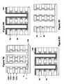
- FIGS. 1A-1Bare respectively side cross sectional and top cross sectional views of a NAND string of one embodiment.
- FIG. 1Ais a side cross sectional view of the device along line Y-Y′ in FIG. 1B
- FIG. 1Bis a side cross sectional view of the device along line X-X′ in FIG. 1A .
- FIGS. 2A-2Bare respectively side cross sectional and top cross sectional views of a NAND string of another embodiment.
- FIG. 2Ais a side cross sectional view of the device along line Y-Y′ in FIG. 2B
- FIG. 2Bis a side cross sectional view of the device along line X-X′ in FIG. 2A .
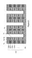
- FIGS. 3-4are side cross sectional views of NAND strings of another two embodiments.
- FIGS. 5A-5Billustrate a first step of a method of making a NAND string according to a first embodiment of the invention.
- FIG. 5Ais a perspective view and
- FIG. 5Bis a side cross sectional view along line Y-Y′ in FIG. 5A .
- FIGS. 6-13are side cross sectional views illustrating steps of the method of making a NAND string according to the first embodiment of the invention.
- FIGS. 14-21illustrate steps of the method of making NAND strings shown in FIGS. 3 and 4 according to an embodiment of the invention.
- FIG. 14Ais a side cross sectional view.
- FIG. 14Bis a top cross sectional view along line X-X′ in the side cross sectional view shown in FIG. 14A
- FIG. 14Cis a top cross sectional view along line Z-Z′ in the side cross sectional view shown in FIG. 14A
- FIG. 14Ais a side cross sectional view along line Y-Y′ in the top cross sectional views shown in FIGS. 14B and 14C .
- FIGS. 15-21are side cross sectional views of the method steps, except that FIG. 18B is a side cross sectional view along line Y-Y′ in the perspective view shown in FIG. 18A .
- FIG. 20Bis a side cross sectional view along line Y-Y′ in the perspective view shown in FIG. 20A .
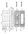
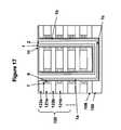
- FIG. 22Ashows a perspective view of a NAND string according to one embodiment of the invention.
- FIG. 22Bis a side cross sectional view along line Y-Y′ in the perspective view shown in FIG. 22A .
- FIGS. 23-27illustrate steps of the method of making the NAND string shown in FIG. 22A-22B according to one embodiment of the invention.
- FIGS. 22B , 23 B, 24 B and 25 Bare side cross sectional views along line Y-Y′ in the perspective views shown in FIGS. 22A , 23 A, 24 A and 25 A, respectively.
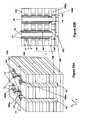
- FIGS. 28A-28Bare side cross sectional views of NAND strings according another two embodiments, respectively.
- FIGS. 29-34illustrate steps of a method of making the NAND string shown in FIG. 28A according to one embodiment of the invention.
- FIG. 29Bis a top cross sectional view along line X-X′ in the side cross sectional view shown in FIG. 29A .
- FIG. 30Bis a top cross sectional view along line X-X′ in the side cross sectional view shown in FIG. 30A .
- FIG. 32Bis a top cross sectional view along line X-X′ in the side cross sectional view shown in FIG. 32A .
- FIGS. 31 , 33 and 34are side cross sectional views.
- FIGS. 35-42illustrate steps of a method of making the NAND string shown in FIG. 28B according to one embodiment of the invention.
- FIG. 35Bis a top cross sectional view along line X-X′ in the side cross sectional view shown in FIG. 35A .
- FIG. 36Bis a top cross sectional view along line X-X′ in the side cross sectional view shown in FIG. 36A .
- FIG. 38Bis a top cross sectional view along line X-X′ in the side cross sectional view shown in FIG. 38A .
- FIGS. 37 and 39 - 42are side cross sectional views.
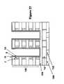
- FIG. 43illustrates a side cross sectional view of a NAND string according to another embodiment.
- FIGS. 44-47illustrate steps of a method of making the NAND string shown in FIG. 43 according to one embodiment of the invention.
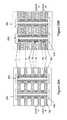
- FIGS. 48 and 49illustrate a side cross sectional view of NAND strings according to other embodiments.
- FIGS. 50-51illustrate steps of a method of making the NAND string shown in FIG. 49 according to one embodiment of the invention.
- FIG. 52illustrates a side cross sectional view of a NAND string according to another embodiment.
- FIGS. 53-57illustrate steps of a method of making the NAND string shown in FIG. 52 according to one embodiment of the invention.
- FIG. 58illustrates a side cross sectional view of a NAND string according to another embodiment.
- FIGS. 59-63illustrate steps of a method of making the NAND string shown in FIG. 58 according to one embodiment of the invention.
- a monolithic three dimensional memory arrayis one in which multiple memory levels are formed above a single substrate, such as a semiconductor wafer, with no intervening substrates.
- non-monolithicmeans that layers of each level of the array are directly deposited on the layers of each underlying level of the array.
- two dimensional arraysmay be formed separately and then packaged together to form a non-monolithic memory device.
- non-monolithic stacked memorieshave been constructed by forming memory levels on separate substrates and adhering the memory levels atop each other, as in Leedy, U.S. Pat. No. 5,915,167, titled “Three Dimensional Structure Memory.” The substrates may be thinned or removed from the memory levels before bonding, but as the memory levels are initially formed over separate substrates, such memories are not true monolithic three dimensional memory arrays.
- the embodiments of the inventionprovide a monolithic, three dimensional array of memory devices, such as an array of vertical NAND strings.
- the NAND stringsare vertically oriented, such that at least one memory cell is located over another memory cell.
- the arrayallows vertical scaling of NAND devices to provide a higher density of memory cells per unit area of silicon or other semiconductor material.
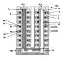
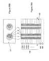
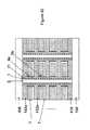
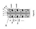
- the monolithic three dimensional NAND string 180comprises a semiconductor channel 1 having at least one end portion extending substantially perpendicular to a major surface 100 a of a substrate 100 , as shown in FIGS. 1A , 2 A, and 3 - 4 .
- the semiconductor channel 1may have a pillar shape and the entire pillar-shaped semiconductor channel extends substantially perpendicularly to the major surface of the substrate 100 , as shown in FIGS. 1A and 2A .
- the source/drain electrodes of the devicecan include a lower electrode 102 provided below the semiconductor channel 1 and an upper electrode 202 formed over the semiconductor channel 1 , as shown in FIGS. 1A and 2A .
- the semiconductor channel 1may have a U-shaped pipe shape, as shown in FIGS. 3 and 4 .
- the two wing portions 1 a and 1 b of the U-shaped pipe shape semiconductor channelmay extend substantially perpendicular to the major surface 100 a of the substrate 100
- a connecting portion 1 c of the U-shaped pipe shape semiconductor channel 1connects the two wing portions 1 a , 1 b extends substantially perpendicular to the major surface 100 a of the substrate 100 .
- one of the source or drain electrodes 202 1contacts the first wing portion of the semiconductor channel from above, and another one of a source or drain electrodes 202 2 contacts the second wing portion of the semiconductor channel 1 from above.
- An optional body contact electrode(not shown) may be disposed in the substrate 100 to provide body contact to the connecting portion of the semiconductor channel 1 from below.
- the NAND string's select or access transistorsare now shown in FIGS. 1-4 for clarity. These transistors are described in more detail below.
- the semiconductor channel 1may be a filled feature, as shown in FIGS. 2A-2B and 4 .
- the semiconductor channel 1may be hollow, for example a hollow cylinder filled with an insulating fill material 2 , as shown in FIGS. 1A-1B and 3 .
- an insulating fill material 2may be formed to fill the hollow part surrounded by the semiconductor channel 1 .
- the substrate 100can be any semiconducting substrate known in the art, such as monocrystalline silicon, IV-IV compounds such as silicon-germanium or silicon-germanium-carbon, III-V compounds, II-VI compounds, epitaxial layers over such substrates, or any other semiconducting or non-semiconducting material, such as silicon oxide, glass, plastic, metal or ceramic substrate.
- the substrate 100may include integrated circuits fabricated thereon, such as driver circuits for a memory device.
- any suitable semiconductor materialscan be used for semiconductor channel 1 , for example silicon, germanium, silicon germanium, or other compound semiconductor materials, such as III-V, II-VI, or conductive or semiconductive oxides, etc. materials.
- the semiconductor materialmay be amorphous, polycrystalline or single crystal.
- the semiconductor channel materialmay be formed by any suitable deposition methods.
- the semiconductor channel materialis deposited by low pressure chemical vapor deposition (LPCVD).
- LPCVDlow pressure chemical vapor deposition
- the semiconductor channel materialmay be a recrystallized polycrystalline semiconductor material formed by recrystallizing an initially deposited amorphous semiconductor material.
- the insulating fill material 2may comprise any electrically insulating material, such as silicon oxide, silicon nitride, silicon oxynitride, or other high-k insulating materials.
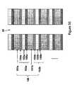
- the monolithic three dimensional NAND stringfurther comprise a plurality of control gate electrodes 3 , as shown in FIGS. 1A-1B , 2 A- 2 B, and 3 - 4 .
- the control gate electrodes 3may comprise a portion having a strip shape extending substantially parallel to the major surface 100 a of the substrate 100 .
- the plurality of control gate electrodes 3comprise at least a first control gate electrode 3 a located in a first device level (e.g., device level A) and a second control gate electrode 3 b located in a second device level (e.g., device level B) located over the major surface 100 a of the substrate 100 and below the device level A.
- the control gate materialmay comprise any one or more suitable conductive or semiconductor control gate material known in the art, such as doped polysilicon, tungsten, copper, aluminum, tantalum, titanium, cobalt, titanium nitride or alloys thereof.
- suitable conductive or semiconductor control gate materialsuch as doped polysilicon, tungsten, copper, aluminum, tantalum, titanium, cobalt, titanium nitride or alloys thereof.
- polysiliconis preferred to allow easy processing.
- a blocking dielectric 7is located adjacent to and may be surrounded by the control gate(s) 3 .
- the blocking dielectric 7may comprise a plurality of blocking dielectric segments located in contact with a respective one of the plurality of control gate electrodes 3 , for example a first dielectric segment 7 a located in device level A and a second dielectric segment 7 b located in device level B are in contact with control electrodes 3 a and 3 b , respectively, as shown in FIGS. 1A-1B , 2 A- 2 B, and 3 - 4 .
- at least a portion of each of the plurality of blocking dielectric segments 7has a clam shape.
- a “clam” shapeis a side cross sectional shape configured similar to an English letter “C”.
- a clam shapehas two segments which extend substantially parallel to each other and to the major surface 100 a of the substrate 100 .
- the two segmentsare connected to each other by a third segment which extends substantially perpendicular to the first two segments and the surface 100 a .
- Each of the three segmentsmay have a straight shape (e.g., a rectangle side cross sectional shape) or a somewhat curved shape (e.g., rising and falling with the curvature of the underlying topography).
- substantially parallelincludes exactly parallel segments as well as segments which deviate by 20 degrees or less from the exact parallel configuration.
- substantially perpendicularincludes exactly perpendicular segments as well as segments which deviate by 20 degrees or less from the exact perpendicular configuration.
- the clam shapepreferably contains an opening bounded by the three segments and having a fourth side open. The opening may be filled by another material or layer.
- the monolithic three dimensional NAND stringalso comprise a plurality of discrete charge storage segments 9 , each of which is located at least partially in an opening of a respective clam-shaped blocking dielectric segment 7 .
- the plurality of discrete charge storage segments 9comprise at least a first discrete charge storage segment 9 a located in the device level A and a second discrete charge storage segment 9 b located in the device level B.
- the tunnel dielectric 11 of the monolithic three dimensional NAND stringis located between each one of the plurality of the discrete charge storage segments 9 and the semiconductor channel 1 .
- the tunnel dielectric 11has a non-uniform thickness and/or a not straight sidewall near the plurality of discrete charge storage segments 9 .
- the tunnel dielectric 11has a uniform thickness and/or a straight sidewall.
- the blocking dielectric 7 and the tunnel dielectric 11may be independently selected from any one or more same or different electrically insulating materials, such as silicon oxide, silicon nitride, silicon oxynitride, or other high-k insulating materials.
- the discrete charge storage segments 9may comprise a conductive (e.g., metal or metal alloy such as titanium, platinum, ruthenium, titanium nitride, hafnium nitride, tantalum nitride, zirconium nitride, or a metal silicide such as titanium silicide, nickel silicide, cobalt silicide, or a combination thereof) or semiconductor (e.g., polysilicon) floating gate, conductive nanoparticles, or a discrete charge storage dielectric (e.g., silicon nitride or another dielectric) feature.
- a conductivee.g., metal or metal alloy such as titanium, platinum, ruthenium, titanium nitride, hafnium nitride, tantalum nitride, zirconium nitride, or a metal silicide such as titanium silicide, nickel silicide, cobalt silicide, or a combination thereof
- semiconductore.g.
- the discrete charge storage segments 9are discrete charge storage dielectric features, each of which comprises a nitride feature located in the respective clam-shaped blocking dielectric segment 7 , where the silicon oxide blocking dielectric segment 7 , the nitride feature 9 and the silicon oxide tunnel dielectric 11 form oxide-nitride-oxide discrete charge storage structures of the NAND string.
- a polysilicon floating gateis used as a non-limiting example. However, it should be understood that a dielectric charge storage feature or other floating gate material may be used instead.
- FIGS. 5-13illustrate a method of making a NAND string according to a first embodiment of the invention.
- a stack 120 of alternating layers 121 ( 121 a , 121 b , etc.) and 122 ( 122 a , 122 b etc.)are formed over the major surface of the substrate 100 .
- Layers 121 , 122may be deposited over the substrate by any suitable deposition method, such as sputtering, CVD, MBE, etc.
- the layers 121 , 122may be 6 to 100 nm thick.
- the first layers 121comprise a first conductive (e.g., metal or metal alloy) or semiconductor (e.g., heavily doped n+ or p+ polysilicon) control gate material
- the second layers 122comprise a second insulating material (e.g., silicon nitride, silicon oxide, etc.).
- heavily dopedincludes semiconductor materials doped n-type or p-type to a concentration of above 10 18 cm ⁇ 3 .
- the deposition of layers 121 , 122is followed by etching the stack 120 to form at least one opening 81 in the stack 120 .
- An array of openings 81may be formed in locations where vertical channels of NAND strings will be subsequently formed.
- first materialis selectively etched compared to the second material 122 to form first recesses 62 in the first layers 121 (i.e., layers 121 a , 121 b , etc).
- the recesses 62may be formed by selective, isotropic wet or dry etching which selectively etches the first material 121 compared to the second material 112 .
- the depth of each recess 62may be 6 to 100 nm.
- a blocking dielectric 7(also known as an inter-poly dielectric, IPD) is then formed in the openings 81 such that the blocking dielectric coats the sides of the first recesses 62 , resulting in a structure as shown in FIG. 6 .
- the blocking dielectric 7may comprise a silicon oxide layer deposited by conformal atomic layer deposition (ALD) or chemical vapor deposition (CVD). Other high-k dielectric materials, such as hafnium oxide, may be used instead or in addition to silicon oxide. Dielectric 7 may have a thickness of 6 to 20 nm.
- the blocking dielectric 7comprises a plurality of clam-shaped blocking dielectric segments (e.g., blocking dielectric segments 7 a and 7 b ) in the first recesses 62 between overhanging portions of the second material 122 .
- a charge storage material 9is formed in the openings 81 and in the first recesses 62 over the blocking dielectric material 7 , resulting in the structure shown in FIG. 7A .
- the charge storage material 9comprises a plurality of discrete charge storage segments (e.g., 9 a and 9 b ) formed inside an opening in a respective one of the plurality of clam-shaped blocking dielectric segments (e.g., 7 a or 7 b ).
- the discrete charge storage segments 9 a , 9 bare connected to each other by outer portions of the charge storage material 9 layer which extends in the openings 81 adjacent to the protruding portions of the second material 122 .
- the discrete charge storage material 9may comprise a charge storage dielectric material (e.g., silicon nitride discrete charge storage dielectric feature).
- the discrete charge storage materialmay comprise a conductive or semiconductor floating gate material (e.g., a metal, metal alloy such as TiN, metal silicide, or heavily doped polysilicon floating gate material). Any desired methods may be used to form the charge storage material 9 , such as ALD or CVD.
- the outer portions of the charge storage material 9 which extend in the openings 81 adjacent to the protruding portions of the second material 122can then be removed to separate the discrete charge storage segments (e.g., 9 a and 9 b ) from each other, resulting in a structure shown in FIG. 8A .
- the outer portions of the blocking dielectric 7 which extend in the openings 81 adjacent to the protruding portions of the second material 122can then be removed to separate the discrete blocking dielectric (e.g., 7 a and 7 b ) from each other if desired.
- the charge storage material and the blocking dielectric materialmay be anisotropically dry or wet etched in the openings 81 in one step or two separate steps to leave the charge storage material 9 only in the recesses 62 (i.e., inside the clam shaped portions of the blocking dielectric 7 ).
- the anisotropic etchmay be extended to also etch the insulating material 122 to enlarge the size of the openings 81 if desired.
- a thin silicide forming metal layersuch as titanium, cobalt or nickel is formed by any suitable method, such as ALD or sputtering, over the polysilicon floating gates 9 a , 9 b shown in FIG. 8A .
- the floating gates 9 a , 9 bare converted to a metal silicide (e.g., titanium, cobalt, nickel, etc. silicide) by the reaction of the metal and the polysilicon.
- a metal silicidee.g., titanium, cobalt, nickel, etc. silicide
- FIGS. 7B , 8 B, 8 C and 8 Dillustrate alternative methods to form polysilicon floating gate charge storage segments 9 a , 9 b using oxidation or silicidation followed by selective oxide or silicide etch.
- FIG. 7Billustrates structure similar to that of FIG. 7A , where a polysilicon floating gate layer 9 is formed in the openings 81 .
- the floating gate layer 9is partially oxidized by wet or dry oxidation (i.e., oxidation in water vapor or air containing ambient at an elevated temperature) such that polysilicon floating gate charge storage segments 9 a , 9 b in recesses 62 remain unoxidized while the rest of layer 9 (e.g., the outside part over protruding second material 122 ) is converted to a silicon oxide layer 19 a .
- the segments 9 a , 9 bremain unoxidized because the polysilicon layer 9 is thicker in the recesses 62 than outside of the recesses 62 in openings 81 .
- the partial oxidationmay be a timed oxidation which is timed to terminate before the segments 9 a , 9 b are converted to silicon oxide.
- the silicon oxide layer 19 ais selectively etched away using any suitable selective wet or dry etch which selectively etches away silicon oxide compared to polysilicon, such as an oxide wet etch, to leave polysilicon floating gates 9 a , 9 b in the recesses 62 .
- layer 19 ais described as a silicon oxide layer, it may comprise a silicon nitride or silicon oxynitride layer formed by nitriding or oxynitriding the polysilicon layer 9 .
- a silicide forming metal layersuch as a titanium, cobalt, nickel, etc., layer is formed over the floating gate layer 9 in the openings 81 .
- the polysilicon layer 9is then partially converted to a metal silicide layer 19 b (e.g., titanium, cobalt, nickel, etc., silicide) by annealing the structure to partially react layer 9 with the metal layer.
- a metal silicide layer 19 be.g., titanium, cobalt, nickel, etc., silicide
- the polysilicon floating gate charge storage segments 9 a , 9 b in recesses 62are not converted to a silicide while the rest of layer 9 (e.g., the outside part over protruding second material 122 ) is converted to the silicide layer 19 b .
- the segments 9 a , 9 bremain unsilicided because the polysilicon layer 9 is thicker in the recesses 62 than outside of the recesses 62 in openings 81 .
- the partial silicidationmay be a timed silicidation which is timed to terminate before the segments 9 a , 9 b are converted to a silicide.
- the partial silicidationmay be controlled by the relative thicknesses of the polysilicon and metal layers such that excess polysilicon is provided in the recesses 62 which lacks access to sufficient metal to form a silicide. Any remaining portion of the metal layer may be removed from the silicide layer 19 b by selective etching.
- the silicide layer 19 bis selectively etched away using any suitable selective wet or dry etch which selectively etches away a silicide material compared to polysilicon, such as a titanium silicide piranha etch.
- the blocking dielectric 7comprises a plurality of discrete regions 7 a , 7 b , etc.
- the blocking dielectric 7comprises a continuous layer which contains regions 7 a , 7 b in the recesses 62 .
- the plurality of the discrete charge storage segments (e.g., 9 a and 9 b ) separated from each otherare disposed in the recesses between overhanging portions of the second material 122 .
- One advantage of the methods of selectively removing outer portion of the charge storage material layer 9 according to FIGS. 7 B and 8 B- 8 Dis that a potential defect of forming ‘poly-stringers’ on the side wall (i.e., incomplete removal of the outer portion by dry etching methods) may be completely eliminated.
- the selective wet etch of a silicon oxide layer 19 a or a silicide layer 19 bmay result in lower damage to the charge storage segments 9 .
- a tunnel dielectric 11is formed over the side wall of the charge storage material 9 (e.g. the discrete charge storage segments 9 a and 9 b ) and material 122 exposed in the at least one opening 81 , resulting in a structure shown in FIG. 9 .
- the tunnel dielectricis formed over the side wall of the charge storage material 9 (e.g. the discrete charge storage segments 9 a and 9 b ) and the outer portion of the blocking oxide dielectric located on protruding portions material 122 in the at least one opening 81 .
- the tunnel dielectricmay comprise a relatively thin insulating layer (e.g., 4 to 10 nm thick) of silicon oxide or other suitable material, such as oxynitride, oxide and nitride multi layer stacks, or a high-k dielectric (e.g., hafnium oxide).
- the tunnel dielectricmay be deposited by any suitable method, such as ALD, CVD, etc.
- the tunnel dielectric 11may be formed by directly converting (e.g., oxidizing) the outer portion of the semiconductor charge storage material layer 9 in one step, rather than by the two-step process of removing the outer portion of the layer 9 and forming tunnel dielectric 11 over the side wall of the charge storage material 9 in the above described method.
- a polysilicon floating gate layer 9is formed as shown in FIG. 7B .
- the polysilicon layer 9is then partially oxidized in a timed oxidation to form a relatively thin oxide layer 19 a as shown in FIG. 8B .
- Any oxidation method that can provide an oxide with good quality to be used as the tunneling dielectricsuch as a high temperature radical oxidation process, may be used.
- the thin oxide layer 19 ais not removed as shown in FIG. 8D , but is retained in the final device as the tunnel dielectric, as shown in FIG. 8B . Thus, a deposition of a separate tunnel dielectric 11 is not required.
- a semiconductor channel material 1is formed in the at least one opening 81 .
- the semiconductor channel material 1completely fills the at least one opening 81 with a semiconductor channel material, as shown in FIG. 10 .
- the step of forming the semiconductor channel 1 in the at least one openingforms a semiconductor channel material 1 on the side wall(s) of the at least one opening 81 but not in a central part of the at least one opening 81 such that the semiconductor channel material 1 does not completely fill the at least one opening 81 .
- an insulating fill material 2is formed in the central part of the at least one opening 81 to completely fill the at least one opening 81 , as shown in FIG. 11 .
- the channel 1 materialcomprises lightly doped p-type or n-type (i.e., doping below 10 17 cm ⁇ 3 ) silicon material.
- An n-channel deviceis preferred since it is easily connected with n+ junctions.
- a p-channel devicemay also be used.
- the semiconductor channel 1may be formed by any desired methods.
- the semiconductor channel material 1may be formed by depositing semiconductor (e.g., polysilicon) material in the opening 81 and over the stack 120 , followed by a step of removing the upper portion of the deposited semiconductor layer by chemical mechanical polishing (CMP) or etchback using top surface of the stack 120 as a polish stop or etch stop.
- CMPchemical mechanical polishing
- a single crystal silicon or polysilicon vertical channel 1may be formed by metal induced crystallization (“MIC”, also referred to as metal induced lateral crystallization) without a separate masking step.
- MICmetal induced crystallization
- the MIC methodprovides full channel crystallization due to lateral confinement of the channel material in the opening 81 .
- an amorphous or small grain polysilicon semiconductor (e.g., silicon) layer 303can be first formed in the at least one opening 81 and over the stack 120 , followed by forming a nucleation promoter layer 305 over the semiconductor layer 303 , as shown in FIG. 12 .
- the nucleation promoter layer 305may be a continuous layer or a plurality of discontinuous regions.
- the nucleation promoter layermay comprise any desired polysilicon nucleation promoter materials, for example but not limited to nucleation promoter materials such as Ge, Ni, Pd, Al or a combination thereof.
- the amorphous or small grain semiconductor layer 303can then be converted to a large grain polycrystalline or single crystalline semiconductor layer 301 by recrystallizing the amorphous or small grain polycrystalline semiconductor, resulting in a structure illustrated in FIG. 13 .
- the recrystallizationmay be conducted by a low temperature (e.g., 300 to 600 C) anneal.
- the upper portion of the polycrystalline semiconductor layer 301 and the nucleation promoter layer 305can then be removed by CMP or etchback using top surface of the stack 120 as a stop, resulting in the structure as shown in FIG. 10 .
- the removalmay be conducted by selectively wet etching the remaining nucleation promoter layer 305 and any formed silicide in the top of layer 301 following by CMP of the top of silicon layer 301 using the top of the stack 120 as a stop.
- an upper electrode 202may be formed over the semiconductor channel 1 , resulting in a structure shown in FIG. 1 or 2 .
- a lower electrode 102may be provided below the semiconductor channel 1 prior to the step of forming the stack 120 over the substrate 100 .
- the lower electrode 102 and the upper electrodemay be used as the source/drain electrodes of the NAND string.
- the source/drain electrodes of the NAND stringcan both be formed over the semiconductor channel 1 and the channel 1 has a U-shaped pipe shape, for example as shown in FIGS. 3 and 4 .
- an optional body contact electrode(as will be described below) may be disposed on or in the substrate 100 to provide a body contact to the connecting portion of the semiconductor channel 1 from below.
- a “U-shaped pipe” shapeis side cross sectional shape configured similar to an English letter “U”.
- This shapehas two segments (referred to herein as “wing portions”) which extend substantially parallel to each other and substantially perpendicular to the major surface 100 a of the substrate 100 .
- the two wing portionsare connected to each other by a connecting segment or portion which extends substantially perpendicular to the first two segments and substantially parallel to the surface 100 a .
- Each of the three segmentsmay have a straight shape (e.g., a rectangle side cross sectional shape) or a somewhat curved shape (e.g., rising and falling with the curvature of the underlying topography).
- substantially parallelincludes exactly parallel segments as well as segments which deviate by 20 degrees or less from the exact parallel configuration.
- substantially perpendicularincludes exactly perpendicular segments as well as segments which deviate by 20 degrees or less from the exact perpendicular configuration.
- FIGS. 14-21illustrate a method of making a NAND string having a U-shaped pipe shape semiconductor channel according to the second embodiment of the invention.
- the substrate 100 shown in FIG. 14may comprise a semiconductor substrate optionally containing embedded conductors and/or various semiconductor devices.
- the substrate 100may comprise an insulating or semiconductor layer optionally containing embedded conductors.
- a sacrificial feature 89may be formed in and/or over the substrate 100 , prior to the step of forming the stack 120 of alternating layers of the first material and second materials over the at least one sacrificial feature 89 .
- the sacrificial feature 89may be formed of any suitable sacrificial material which may be selectively etched compared to the other materials in the stack 120 and in the NAND string, such as an organic material, silicon nitride, tungsten, etc.
- Feature 89may have any suitable shape which is similar to the desired shape of the connecting segment of the U-shape as will be described below.
- An insulating protective layer 108may be formed between the sacrificial feature 89 and the stack 120 .
- layer 108may comprise silicon oxide if feature 89 comprises silicon nitride.
- FIG. 14Ashows a top cross sectional view along line X-X′ in FIG. 14A .
- FIG. 14Cshows a top cross sectional view along line Z-Z′ in FIG. 14C .
- FIG. 14Ais a side cross sectional view along line Y-Y′ in FIGS. 14B and 14C .
- the openings 81 and 82are formed above the sacrificial feature 89 , as illustrated in FIGS. 14A-C .
- the semiconductor channelhas a cross section of two circles when viewed from above, as shown in FIG. 14B .
- the protective layer 108is used as a stop for the etching of the openings 81 , 82 such that the top of layer 108 forms the bottom surface of the openings 81 , 82 .
- the at least one sacrificial feature 89is then removed to form a hollow region 83 where the feature 89 was located.
- the hollow region 83extends substantially parallel to a major surface 100 a of the substrate 100 , and connects the at least two openings 81 and 82 , forming a hollow U-shaped pipe space 80 .
- the hollow region 83may be formed by further etching the openings 81 , 82 (e.g., by anisotropic etching) such that these openings extend through the protective layer 108 to expose the sacrificial feature 89 .
- the sacrificial feature 89 materialis then selectively etched using a selective wet or dry etch which selectively removes the sacrificial feature material without substantially etching material 122 , blocking dielectric 7 and charge storage segments 9 .
- a tunnel dielectric 11 and a semiconductor channel 1 over the tunnel dielectric 11may be formed in the hollow U-shaped pipe space 80 .
- the step of forming the semiconductor channel 1 on the side wall of the hollow U-shaped pipe space 80may completely fill the hollow U-shaped pipe space 80 with the semiconductor channel material as shown in FIG. 4 .
- the step of forming the semiconductor channel 1 in the hollow U-shaped pipe space 80forms a semiconductor channel material on the side wall of the hollow U-shaped pipe space 80 but not in a central part of the hollow U-shaped pipe space 80 such that the semiconductor channel material does not completely fill the hollow U-shaped pipe space 80 .
- an insulating fill material 2is then formed in the central part of the semiconductor channel 1 to completely fill the hollow U-shaped pipe space 80 , resulting in a structure shown in FIG. 17 (also shown in FIG. 3 ).
- the semiconductor channel 1substantially adopts the shape of the hollow U-shaped pipe space 80 , which includes the first and second vertically extending openings 81 and 82 and horizontally extending space 83 .
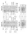
- the stack 120is then etched to form a rail shaped gate cut, which is then filled by an insulating material 185 , such as silicon oxide, etc., to electrically isolate the control gate electrodes 3 surrounding the two wing portions of the semiconductor channel 1 from etch other, resulting in a device shown in FIGS. 18A (perspective view) and 18 B (side cross sectional view along line Y-Y′ in FIG. 18A ).
- an insulating material 185such as silicon oxide, etc.
- a source or drain electrodemay the be formed to contact the wing portion of the semiconductor channel 1 located in the first opening 81 and the other drain or source electrode contacts the other wing portion of the semiconductor channel 1 located in the second opening 82 .
- the drain electrodeconnects to the NAND string channel through a drain select transistor 203 a (also referred to as SGD device) and the source electrode connects to the other side of the NAND string channel through a source select transistor 203 b (also referred to as SGS device).
- SGD devicealso referred to as SGD device
- SGS devicesource select transistor 203 b
- the gate cut stepcan then be performed to separate the select transistors 203 a and 203 b from each other in the same step as the step separating the control gate electrodes 3 surrounding the two wing portions of the semiconductor channel 1 , resulting in a structure shown in FIGS. 20A (perspective view) and 20 B (cross sectional view along lines Y-Y′ in FIG. 20B ).
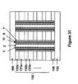
- a cutis made between the select transistors of adjacent NAND strings, such as between adjacent SGD devices 203 a of adjacent strings as shown in FIG. 21 .
- an insulating material 187such as silicon oxide, etc., is formed in the cut between the select transistors, resulting in an array of NAND strings 180 as shown in FIG. 21 .
- the semiconductor channel 1may have a “small” U-shaped side cross section, as shown in FIGS. 22A (perspective view) and 22 B (cross sectional view along line Y-Y′ in FIG. 22A ).
- each wing 1 a , 1 b of the U-shaped pipe shapewas formed in a separate opening 81 , 82 .
- both wings of the “small” U-shapeare formed in the same opening.
- the two wing portions 1 w and 1 w ′ of the U-shaped semiconductor channel 1are formed in the same opening 81 .
- the wing portionextend substantially perpendicular to a major surface 100 a of the substrate 100 and are connected by a connecting portion 1 w ′′ at the bottom of the opening 81 .
- the connecting portionextends substantially parallel to the major surface 100 a of the substrate 100 .
- an a plurality of U-shaped NAND stringsis formed in each opening 81 .
- the first NAND string 180 a in each opening 81includes wings 1 w and 1 w ′.
- the second NAND string 180 b in each openingincludes wings 1 x and 1 x ′, and so on.
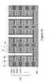
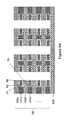
- the NAND stringsmay be arranged in a grid shaped array, which includes one set strings 180 a , 180 b arranged in a first horizontal “z” direction (i.e., parallel to major surface 100 a of the substrate 100 ) in the each elongated trench shaped opening 81 , and a second set of strings 180 a , 180 a in a second horizontal second “x” direction (i.e., parallel to the major surface 100 a and perpendicular to the z direction) in each adjacent opening 81 .
- first horizontal “z” directioni.e., parallel to major surface 100 a of the substrate 100
- second set of strings 180 a , 180 a in a second horizontal second “x” directioni.e., parallel to the major surface 100 a and perpendicular to the z direction
- FIGS. 23-27illustrate a method of making a NAND string having semiconductor channel with the “small” U-shaped side cross section shown in FIGS. 22A-B according to the third embodiment of the invention.
- a connecting feature 1 w ′′may be formed in and/or over the substrate 100 , prior to the step of forming the stack 120 of alternating layers of the first material and second materials over the connecting feature 1 w ′′.
- the connecting feature 1 w ′′may be a semiconductor or conductor region formed in or over the substrate 100 .
- the connecting feature 1 w ′′may comprise a semiconductor or conductor region enclosed by the protective insulating layer 100 b and embedded in the semiconductive layer 100 a , as shown in FIG. 22B .
- Features 1 w ′′may be formed by a damascene process in the trenches in layer 100 a .
- features 1 w ′′may be formed by lithographically patterning a conductive or semiconductor layer to form the features 1 w ′′ followed by forming the insulating layer 100 b and semiconducting layer 100 a around the features 1 w′′.
- the at least one opening 81is then formed in the stack 120 , resulting in a structure as shown in FIG. 23A (perspective view) and 23 B (cross sectional view along line Y-Y′ in FIG. 23A ).
- the opening 81has a square or rectangular shaped top cross-section as shown in FIG. 23A .
- Other shapesfor example a circular shape, may be used if desired.
- An optional body contact electrode 102may be provided in or over the substrate 100 to contact the connecting portion feature 1 w ′′ from below.
- the blocking dielectric 7 and the plurality of discrete charge storage segments 9 , and the tunnel dielectric layer 11can then be formed using methods described above with respect to the first embodiment and FIGS. 5-13 , resulting in a structure shown in FIGS. 24A and 24B .
- a bottom portion of the tunnel dielectric layer 11 located over the bottom of the at least one opening 81 and the insulating protective layer 108 located below the bottom portion of the tunnel dielectric layer 11are then etched (e.g., by anisotropic etching) to expose the semiconductor connecting feature 1 w ′′ in the opening 81 , resulting in a structure shown in FIG. 25B .
- the tunnel dielectric layer 11is also removed from the top of the stack during the same etching step.
- the tunnel dielectric layer 11remains on the sidewall(s) of the opening similar to a side wall spacer.
- the semiconductor channel materialcan then be formed in the openings 81 using methods described above. Similarly, the semiconductor channel material may completely or partially fill the opening 81 . Then, the middle portion of the semiconductor channel material is etched to form the two wings portions 1 w and 1 w ′ of the U-shaped semiconductor channel 1 , resulting in the structure shown in FIGS. 22A-B . As shown in FIG. 22B , the two wing portions 1 w and 1 w ′ of the U-shaped semiconductor channel 1 are electrically connected by the connecting portion 1 w ′′ (i.e., the connecting feature 1 w ′′) which extends substantially parallel to the major surface of the substrate 100 .
- the connecting portion 1 w ′′i.e., the connecting feature 1 w ′′
- the connecting feature 1 w ′′ connecting the two wing portions of the semiconductor channel 1 w and 1 w ′may be formed during the step of etching the middle portion of the semiconductor material by leaving a bottom portion of the semiconductor material filling openings 81 unetched, rather than being provided below the stack and exposed prior to the step of forming the semiconductor material.
- an insulating fill 2is formed over the connecting feature 1 w ′′ and between the two separated wing portions 1 w and 1 w ′ of the U-shaped semiconductor channel 1 as shown in FIG. 26 .
- source and drain electrodes 202 1 and 202 2may be formed over the semiconductor channel 1 as shown in FIGS. 3 and 4 .
- One of the select transistors 203 acontacts the first wing portion 1 w from above, and another one of the select transistors 203 b contacts the second wing portion 1 w ′ from above, as shown in FIG. 26 .
- a masking spacer layer 14may be formed over portions of the tunneling dielectric layer 11 located on the side wall of the at least one opening 81 such that the bottom portion of the tunnel dielectric 11 remains exposed, as shown in FIG. 27 .
- the masking spacer layer 14protects the tunnel dielectric 11 from being damaged during the step of etching the bottom portion of the tunnel dielectric and the protective layer 108 .
- the masking spacer layer 14may be removed during or after the steps of etching the bottom portion of the tunnel dielectric layer 11 and the insulating protective layer 108 .
- the spacer layer 14may comprise any material which has a lower etch susceptibility than the material of layer 11 to the etching medium used to etch the bottom of layer 11 .
- the tunnel dielectric layer 11is silicon oxide
- spacer layer 14may be silicon nitride.
- the spacer layermay be formed by typical sidewall spacer formation methods, such as forming layer 14 on the sidewall(s) and bottom of the openings 81 and then anisotropically etching layer 14 to leave only sidewall spacer portions of layer 14 over layer 11 on the sidewall(s) of the openings, as shown in FIG. 27 .
- the monolithic three dimensional NAND stringis formed by using an alternative method from that of the first three embodiments to form relatively thin floating gate charge storage segments 9 .
- the resulting vertical NAND string of this embodimentalso includes a tunnel dielectric 11 with a straight sidewall and a uniform thickness.
- the tunnel dielectric 11 of the first three embodimentsmay have a slightly curved sidewall if the charge storage segments 9 protrude into the opening 81 past material 122 or if material 122 protrudes into the opening 81 past the segments 9 . This may cause a curve in the sidewall of the tunnel dielectric and a variation in thickness of the tunnel dielectric 11 as it curves around the protrusions in the opening 81 .
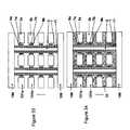
- each of the discrete charge storage segments 9may have a height shorter than that of the respective control gate electrode 3 in the same device level.
- a first discrete charge storage segment 9 amay have a height shorter than that of a first control gate electrode 3 a and a second discrete charge storage segment 9 b has a height shorter than that of a second control gate electrode 3 b , as shown in FIG. 28A .
- the term “height”means a vertical direction perpendicular to the major surface 100 a of the substrate 100 .
- each of the first discrete charge storage segment 9may have a height greater than that of the respective control gate electrode 3 of the same memory cell.
- a first discrete charge storage segment 9 amay have a height greater or longer than that of a first control gate electrode 3 a and a second discrete charge storage segment 9 b has a height greater or longer than that of a second control gate electrode 3 b , as shown in FIG. 28B .
- the select transistorsare omitted for clarity from FIGS. 28A and 28B .
- FIGS. 29-34illustrate a method of making a NAND string shown in FIG. 28A , according to one embodiment of the invention.
- a stack 130 of alternating layers of a conductive or semiconductor control gate material layers 131e.g., 131 a , 131 b , etc.
- a sacrificial material layer 132e.g., 132 a , 132 b , etc.
- the sacrificial materialmay comprise any desirable materials that can be selectively etched compared to the conductive or semiconductor control gate material.
- the control gate material layers 131comprise a polysilicon or tungsten control gate material
- the sacrificial material layers 132may comprise an oxide, such as silicon oxide.
- the stack 130may then be etched to form at least one opening 81 in the stack 130 .
- the opening 81may extend to the major surface 100 a of the substrate 100 or to the protective layer 108 .
- FIG. 29Bshows a top cross sectional view along line X-X′ in FIG. 29A .
- a blocking dielectric layer 7can be formed on a side wall of the at least one opening 81 .
- the step of forming the semiconductor channel layer 1 in the at least one opening 81does not completely fills the at least one opening 81 .
- an insulating fill material 2is then formed in the central part of the at least one opening 81 to completely fill the at least one opening 81 , resulting in a structure shown in FIGS. 30A (side cross sectional view) and 30 B (top cross sectional view).
- the fill material 2may be omitted when the step of forming the semiconductor channel layer 1 in the at least one opening 81 completely fills the at least one opening 81 with a semiconductor channel material.
- FIG. 31another insulating layer 106 is then formed over the stack 130 .
- the sacrificial material layers 132may then be removed to expose the blocking dielectric layer 7 between the control gate material layers 131 (including between the control gate material layers 131 a and 131 b ), resulting in a structure as shown in FIG. 32A .
- the sacrificial material layers 132are removed from the back side of the stack 130 , rather than through the opening(s) 81 .
- the cut area(s) 84 of the stack 130are removed first.
- a top view of a resulting structure according to a non-limiting exampleis shown in FIG. 32B .
- the cut area(s) 84may be formed by forming a mask by photolithography followed by etching the unmasked cut areas.
- the blocking dielectric layer 7 and the charge storage material layer 9can then be etched using the first material layers 131 as a mask to form a plurality of separate discrete charge storage segments 9 a , 9 b , etc., and separate discrete blocking dielectric segments 7 a , 7 b , etc.
- the step of etching the blocking dielectric layer 7 and the discrete charge storage material layer 9undercut the blocking dielectric layer 7 and the discrete charge storage material layer 9 such that the discrete charge storage segments 7 a , 7 b and the blocking dielectric segments 9 A and 9 B are shorter than the thickness (i.e., vertical dimension) of the first material layers 131 a and 132 a respectively (i.e., the thickness of the control gates in a respective device level), resulting in a structure as shown in FIG. 33 .
- An insulating fill material 33can then be formed between the first material layers 131 , between the blocking dielectric segments 7 and between the discrete charge storage segments 9 resulting in vertical NAND strings shown in FIG. 34 .
- an upper electrode 202may be formed over the semiconductor channel 1 , resulting in a structure shown in FIGS. 28A .
- a lower electrode 102may be provided below the semiconductor channel 1 prior to the step of forming the stack 130 over the substrate 100 .
- the lower electrode 102 and the upper electrode 202may be used as the source/drain electrodes of the NAND string.
- the select transistorsare not shown for clarity in FIG. 28A . These transistors may be located at the top and bottom of a linear NAND string shown in FIG. 28A or at the top of a U-shaped NAND string of the second and third embodiments which can be made by the backside etching method of this fourth embodiment.
- the resulting NAND string 280may comprise a plurality of device levels over the substrate 100 .
- Each of device levelscomprise a respective control gate 3 , a respective blocking dielectric segment adjacent 7 to the respective control gate 3 , a respective discrete charge storage segment 9 adjacent to respective blocking dielectric segment 7 , a respective portion of the tunnel dielectric layer 11 adjacent to the respective discrete charge storage segment 9 , and a respective portion of the channel layer 1 .
- the discrete charge storage segments 9have a height shorter than that of the control gate electrodes 3 in each respective device level.
- the monolithic three dimensional NAND stringmay further comprise one of a source or drain electrode 202 which contacts the semiconductor channel 1 from above, and another one of a source or drain electrode 102 which contacts the semiconductor channel from below.
- FIG. 35-42illustrate a methods of making a NAND string 380 shown in FIG. 28B , according to another aspect of the fourth embodiment of the invention.
- a stack 140 of alternating layers of a first sacrificial material 141(e.g., 141 a , 141 b , etc.) and a second sacrificial material 142 (e.g., 142 a , 142 b , etc.) are formed over a bottom sacrificial layer 408 located over a substrate 100 .
- the sacrificial materials of layers 141 , 142 and 408may be any desired materials such that the first sacrificial material 141 and the bottom sacrificial material 408 can be selectively etched compared to the second sacrificial material 142 .
- the first sacrificial material 141 and the bottom sacrificial material 408may comprise an oxide (e.g., silicon oxide).
- the second sacrificial material 142may comprise a doped polysilicon
- the first sacrificial material 141 and the bottom sacrificial material 408may comprise an undoped polysilicon.
- the stack 140may then be etched to form at least one opening 81 in the stack 140 .
- a discrete charge storage material layer 9is formed on a side wall of the at least one opening 81 , followed by forming a tunnel dielectric layer 11 on the charge storage material layer 9 , and a semiconductor channel layer 1 on the tunnel dielectric layer 11 in the at least one opening 81 .
- the step of forming the semiconductor channel layer 1 in the at least one opening 81does not completely fills the at least one opening 81 .
- an insulating fill material 2is then formed in the central part of the at least one opening 81 to completely fill the at least one opening 81 , resulting in a structure shown in FIGS.
- the fill material 2may be omitted when the step of forming the semiconductor channel layer 1 in the at least one opening 81 completely fills the at least one opening 81 with a semiconductor channel material.
- an insulating layer 406is then formed over the stack 140 .
- the second sacrificial material layers 142 and the bottom sacrificial material 408may then be selectively removed without removing the first material layers 141 , resulting in a structure shown in FIG. 38A .
- cut areas 94 through the stack 140 shown in FIG. 38Bmay be removed prior to the step of selectively removing the second sacrificial material layers 142 to open access to the back side of the stack 140 .
- a resulting structure according to a non-limiting exampleis shown in FIG. 38A (side cross sectional view) and 38 B (top cross sectional view along line X-X′ in FIG. 38A ).
- the charge storage material layer 9can then be etched using the first sacrificial material layers 141 as a mask to form a plurality of separate discrete charge storage segments, such as 9 a and 9 b , etc, resulting in a structure shown in FIG. 39 .
- an optional etch stop layer(not shown) may be formed on the sidewall of the at least one opening 81 prior to the step of forming the charge storage material layer 9 .
- the optional etch stop layeris etched using the first material layers 141 a mask to expose portions of a side of the charge storage material layer 9 between the first material layers 141 , prior to the step of etching the charge storage material layer 9 using the first sacrificial material layers 141 as a mask.
- an insulating material 143(for example layers 143 a , 143 b , etc) is formed between the first material layers 141 to form alternating layers of insulating material layers 143 and the first material layers 141 through the backside from the cut area region 94 .
- the isolating layer materialis than etched out from the cut region 94 .
- a bottom insulating layer 418may also be formed between the stack 140 and the substrate 100 in the same step, filling the space originally occupied by the bottom sacrificial layer 408 shown in FIG. 36A .
- first material layers 141are then selectively removed to expose side wall of the discrete charge storage segments 9 using insulating material 143 as a mask.
- Thisis followed by forming a blocking dielectric 7 on the side wall of the discrete charge storage segments 9 and on the surfaces of the insulating material layers 143 exposed in the space previously occupied by layers 141 between the insulating material layers 143 , resulting in a structure shown in FIG. 41 .
- the blocking dielectric 7has a “reverse” clam shape where the open side of the clam shape faces away from the opening 81 rather than toward it. Control gates 3 can then be formed in the empty space in the clam shaped blocking dielectric 7 between the insulating material layers 143 , resulting in a structure shown in FIG. 42 .
- the isolated control gates 3may be formed by depositing a conductor (e.g., depositing tungsten by CVD) in the empty space in the clam shaped blocking dielectric 7 and the cut region 94 , followed by subsequently etching out the portion of conductor located in the cut region 94 .
- a conductore.g., depositing tungsten by CVD
- An upper electrode 202may be formed over the semiconductor channel 1 , resulting in a structure shown in FIG. 28B .
- a lower electrode 102may be provided below the semiconductor channel 1 prior to the step of forming the stack 140 over the substrate 100 .
- the lower electrode 102 and the upper electrode 202may be used as the source/drain electrodes of the NAND string. As described with respect to FIG. 28A above, the select transistors are not shown in FIG. 28B for clarity.
- the resulting NAND string 380may comprise a plurality of device levels over the substrate 100 .
- Each of device levelscomprise a respective control gate 3 , a respective blocking dielectric segment adjacent 7 to the respective control gate 3 , a respective discrete charge storage segment 9 adjacent to respective blocking dielectric segment 7 , a respective portion of the tunnel dielectric layer 11 adjacent to the respective discrete charge storage segment 9 , and a respective portion of the channel layer 1 .
- At least a portion of each of the blocking dielectric segments 7 of the NAND stringhas a clam shape and each of the plurality of control gate electrodes 3 of the NAND is located at least partially in an opening in the clam-shaped portion of a respective blocking dielectric segment 7 .
- the discrete charge storage segments 9have a height greater than that of the control gate electrodes 3 in each respective device level because the charge storage segments 9 have the same height as the reverse clam shaped blocking dielectric 7 , while the control gate electrodes 3 are located inside the reverse clam shaped blocking dielectric 7 .
- the monolithic three dimensional NAND stringmay further comprise one of a source or drain electrode 202 which contacts the semiconductor channel 1 from above, and another one of a source or drain electrode 102 which contacts the semiconductor channel from below.
- hollow U-shaped pipe spacemay be formed rather than openings 81 shown in FIGS. 29A and 35A .
- the semiconductor channel 1substantially adopts the shape of the hollow U-shaped pipe space, rather than having a pillar shape (as shown in FIGS. 28A and 28B ).
- two upper electrodesmay be used as the source/drain electrodes of the NAND string contacting the semiconductor channel from above, with an optional lower electrode contacting the bottom portion of the semiconductor channel as a body contact, as shown in FIGS. 3 , 4 and 22 B.
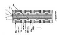
- At least a first conductive or semiconductor (e.g., heavily doped semiconductor) shielding wingis located between a first discrete charge storage segment and a second discrete charge storage segment.
- the shielding wingreduces parasitic coupling between adjacent cells in each vertical NAND string through the insulating material which separates each cell from an adjacent cell located above or below.
- a shielding wing 12 ais located between the charge storage segment 9 a located in device level A and charge storage segment 9 b located in device level B of the NAND string 480 .
- the device level Bis located over the major surface of the substrate (not shown for clarity in FIG. 43 ) and below the device level A.
- the shielding wing 12 ais located in electrical contact with control gate electrode 3 a in the same device level (i.e., device level A).
- Wing 12 amay comprise a portion of a conductive or semiconductor layer located between adjacent, vertically separated cells and which protrudes into the space (e.g., opening 81 ) between charge storage segments 9 .
- Wing 12may comprise any conductive material, such as a metal or metal alloy, e.g., tungsten, titanium nitride, titanium silicide etc., or semiconductor material, such as heavily doped polysilicon.
- each of the plurality of blocking dielectric segments 7has a clam shape and each of the plurality of discrete charge storage segments 9 is located at least partially in an opening in a respective clam-shaped blocking dielectric segment 7 .
- FIG. 44-48illustrate a method of making a NAND string 480 shown in FIG. 43 , according to the fifth embodiment of the invention.
- first layers 151e.g., 151 a in device level A and 151 b in device level B
- the first layers 151comprise a conductive or semiconductor control gate material, such as heavily doped polysilicon.
- the second layers 152(e.g., 152 a in device level A and 152 b in device level B) comprise an insulating sub-layer 153 (e.g., 153 a in device level A and 153 b in device level B), such as silicon oxide, and a first sacrificial sub-layer 154 (e.g., 154 a in device level A and 154 b in device level B) of a different material (such as silicon nitride) than sub-layer 153 .
- the stack 150is then etched to form at least one opening 81 in the stack as in the prior embodiments, resulting in a structure shown in FIG. 44 .
- a blocking dielectric 7is then formed in the opening 81 and in the first recesses 62 , and a plurality of discrete charge storage segments 9 separated from each other are formed in the first recesses 62 over the blocking dielectric 7 using methods described in the previous embodiment.
- the step of forming the blocking dielectric 7 in the first recesses 62comprises forming a plurality of clam-shaped blocking dielectric segments 7 in the first recesses 62
- the step of forming the plurality of discrete charge storage segments 9comprises forming each of the plurality of discrete charge storage segments 9 inside an opening in a respective one of the plurality of clam-shaped blocking dielectric segments 7 .
- a tunnel dielectric 11can then be formed over a side wall of the discrete charge storage segments 9 exposed in the at least one opening 81 , followed by forming a semiconductor channel 1 in the at least one opening 81 , using methods described above.
- the step of forming the semiconductor channel 1 in the at least one opening 81forms a semiconductor channel material 1 on the side wall of the at least one opening 81 but not in a central part of the at least one opening 81 such that the semiconductor channel material 1 does not completely fill the at least one opening 81 .
- An insulating fill material 2 in the central part of the at least one opening 81 to completely fill the at least one opening 81resulting a structure shown in FIG. 46 .
- the semiconductor channel material 1completely fills (not shown) the at least one opening 81 with a semiconductor channel material.
- a cut area (not shown for clarity) of the stack 150is then etched to expose a back side of the stack 150 using methods described in the previous embodiments (e.g., as shown in FIG. 32B ). This is followed by removing the first sacrificial sub-layers 154 to form second recesses 64 (e.g., recess 64 a in device level A and recess 64 b in device level B) from the back side of the stack through the cut area, resulting in a structure shown in FIG. 47 .
- second recesses 64e.g., recess 64 a in device level A and recess 64 b in device level B
- the sacrificial sub-layers 154comprise silicon nitride
- these sub-layersmay be removed by a selective wet etch which selectively etches silicon nitride compared to polysilicon and silicon oxide.
- Wings 12may comprise ALD or CVD deposited tungsten layers which are provided through the cut region. After wings 12 are deposited through the cut region, the cut region may be etched out.
- each first sacrificial sub-layer 154is located above the insulating sub-layer 153 in each second layer 152 .
- the first sacrificial sub-layer 154 a in device level Ais located above the insulating sub-layer 153 a in device level A
- the first sacrificial sub-layer 154 b in device level Bis located above the insulating sub-layer 153 b in device level B.
- the wings 12are located above each respective sub-layer 153 and below each respective control gate 3 in each memory cell.
- the first sacrificial sub-layers 154may be located below, rather than above, the insulating sub-layer 153 in each second layer 152 .
- the wings 12are located below each respective sub-layer 153 and below each respective control gate 3 in each memory cell, as shown in FIG. 48 .
- wing 12 ais in electrical contact with gate 3 b of the next cell.
- wing 12 amay be considered to be part of the cell in level B since this wing is connected to the control gate in level B.
- each of the plurality of shielding wings 12is located between adjacent two of the plurality of discrete charge storage segments 9 .
- the shielding wing 12 ais located between the discrete charge storage segments 9 a and 9 b.
- the NAND stringcontains two shielding wings per cell as shown in FIG. 49 .
- each cellfurther comprises a second conductive or semiconductor shielding wing 13 b located in electrical contact with the control gate electrode 3 b (i.e., each gate contacts a wing above and a wing below the gate).
- Wing 13 bextends substantially parallel to the major surface of the substrate 100 and at least partially between the first discrete charge storage segment 9 a and the second discrete charge storage segment 9 b , as shown in FIG. 49 .
- two shielding wingsfor example shielding wing 12 a and shielding wing 13 b , are located between discrete charge storage segments 9 a and 9 b , as shown in FIG. 49 .
- the shielding wings located in the same device levelare separated from each other by the first layer 151 (i.e., the control gate 3 in these embodiments), while the shielding wings located in adjacent device levels are electrically isolated from each other by the interlevel insulating layers (e.g., the insulating sub-layers 153 ).
- the shielding wings 12 a and 13 a located in the device level Aare connected to each other by the first layer 151 a (i.e., control gate 3 a ) while the shielding wing 12 a located in device level A and 13 b located in the device level B are separated from each other by the insulating sub-layer 153 a.
- FIGS. 50-51illustrate a method of making a NAND string shown in FIG. 49 , according to one embodiment of the invention.
- the second sacrificial layer 152 of the stack 150further comprises a second sacrificial sub-layer 155 , where the insulating sub-layer 153 is located below the first sacrificial layer 154 and above the second sacrificial layer 155 .
- the step of removing the first sacrificial sub-layer 154 aalso removes the second sacrificial sub-layer 155 a to form third recesses 66 b in device level B located immediately below the device level A, resulting in a structure shown in FIG. 51 .
- Shielding wings 12 and 13are then formed in the second 64 and third 66 recesses, resulting in the structure shown in FIG. 49 .
- an upper electrode(not shown) may be formed over the semiconductor channel 1
- a lower electrode(not shown) may be provided below the semiconductor channel 1 prior to the step of forming the stack 150 over the substrate 100 .
- the lower electrode and the upper electrodemay be used as the source/drain electrodes of the NAND string.
- At least one sacrificial featuremay be provided over a substrate and below the stack 150 , such that the at least one sacrificial feature can be then removed to form a hollow region extending substantially parallel to a major surface of the substrate which connects the at least one openings and another opening in the stack to form a hollow U-shaped pipe space, prior to the step of forming the tunnel dielectric 11 .
- the step of forming the semiconductor channel 1forms the semiconductor channel in the hollow U-shaped pipe space and adopts the shape of the hollow U-shaped pipe space, as described in the above embodiments.
- the first shielding wings 12 , the second shielding wings 13 and the control gate electrodes 3can be formed in a same step such that each first shielding wing 12 comprises a lower part of a respective control gate electrode 3 and that each second shielding wing 13 comprises an upper part of a respective control gate electrode 3 .
- no observable interfaceexists between the first shielding wing 12 , the second shielding wing 13 and the control gate electrode 3 in each device level.
- each of the control gates 3has a clam shape. For example, as shown in FIG.
- the first shielding wing 12 a , the second shielding wing 13 a and the control gate electrode 3 acan be formed in a same step such that the first shielding wing 12 a comprises a lower part of the control gate electrode 3 a and that the second shielding wing 13 a comprises an upper part of the control gate electrode 3 a .
- the first shielding wing 12 b , the second shielding wing 13 b and the control gate electrode 3 bare formed in a same step (preferably the same step as the gate and wings in level A) such that the first shielding wing 12 b comprises a lower part of the control gate electrode 3 b and that the second shielding wing 13 b comprises an upper part of the control gate electrode 3 b.
- Each first shielding wing 12extends at least partially between a first and an adjacent second of the plurality of the discrete charge storage segments 9 and a second shielding wing 13 extends at least partially between the first and an adjacent third of the plurality of the discrete charge storage segments 9 .
- the first shielding wing 12 aextends at least partially between the discrete charge storage segments 9 a and 9 b
- the second shielding wing 13 aextends at least partially between the discrete charge storage segment 9 a and a discrete charge storage segment of an upper device level (now shown).
- the second shielding wing 13 b in level B and the first shielding wing 12 a in level Aare both located between discrete charge storage segments 9 a and 9 b.
- each of the plurality of blocking dielectric segments 7is located at least partially in an opening in a respective clam-shaped control gate electrode 3 , while the first discrete charge storage segment 9 is disposed at least partially between the shielding wings 12 and 13 in each device level.
- segment or floating gate 9 ais located between wings 12 a and 12 b and adjacent to the side of control gate 3 a .
- the wings 12 , 13 and control gates 3may be made of any suitable conductive or heavily doped semiconductor material, such as tungsten or heavily doped polysilicon.
- FIG. 53-57illustrate a method of making a NAND string 680 shown in FIG. 52 , according to the fifth embodiment of the invention.
- a stack 160 of alternating layers of a first layer 161 and a second layer 162are formed over a substrate (not shown).
- the first layer 161comprises a first sacrificial sub-layer 164 , a second sacrificial sub-layer 165 and a third sacrificial sub-layer 163 located between the first sacrificial sub-layer 164 and the second sacrificial sub-layer 165 .
- the stack 160is then etched to form at least one opening 81 , resulting in a structure shown in FIG. 53 .
- the third sacrificial sub-layer 163is selectively etched to form first recesses 61 , as shown in FIG. 54 .
- a plurality of discrete charge storage segments 9 separated from each othercan then be formed in the first recesses 61 using methods described above, resulting in a structure shown in FIG. 55 .
- the second layer 162comprises an insulating layer, such as silicon oxide.
- the third sacrificial sub-layer 163comprises a sacrificial material different from the first sacrificial sub-layer 164 , the second sacrificial sub-layer 165 , and the second layer 162 .
- the first 164 and second 165 sacrificial sub-layersmay comprise silicon nitride
- the third sacrificial sub-layer 163comprises undoped polysilicon
- the plurality of discrete charge storage segments 9comprise doped polysilicon.
- the step of forming the semiconductor channel 1 in the at least one openingforms a semiconductor channel material on the side wall of the at least one opening 81 but not in a central part of the at least one opening 81 such that the semiconductor channel material 1 does not completely fill the at least one opening 81 , and an insulating fill material 2 is then formed in the central part of the at least one opening 81 to completely fill the at least one opening 81 , resulting a structure shown in FIG. 56 .
- the step of forming the semiconductor channel 1 in the at least one openingcompletely fills the at least one opening 81 with a semiconductor channel material.
- the insulating filler material 2may be omitted.
- the stack 160can then be etched to expose a back side of the stack 160 , such as through a cut region similar to the one shown in FIG. 32B . This is then followed by removing the first sacrificial sub-layer 164 , the second sacrificial sub-layer 165 and the third sacrificial sub-layer 163 from the back side of the stack through the cut region to form clam shaped openings 86 such that the plurality of discrete charge storage segments 9 and portions of the tunneling dielectric 11 are exposed in the clam-shaped openings 86 between layers 162 , as shown in FIG. 57 .
- a blocking dielectric layeris then formed on the stack from the back side such that a plurality of clam-shaped blocking dielectric segments 7 are formed in the clam shaped openings 86 around and over the plurality of discrete charge storage segments 9 . Each segment 7 partially fills the respective opening 86 .
- the partially filled openingsare then filled by forming a plurality of clam shaped control gate electrodes 3 in the clam shaped openings 86 that are partially filled by the clam shaped blocking dielectric segments 7 , resulting in a structure shown in FIG. 52 .
- a conductive or semiconductor liner(e.g., 15 a ) is located between the control gate electrodes (e.g., 3 a ) and blocking dielectric segments (e.g., 7 a ) of NAND string 680 shown in FIG. 58 .
- the conductive or semiconductor liner 15has a clam shape and comprises a first shielding wing 12 and a second shielding wing 13 connected by a connection portion such that the first discrete charge storage segment 9 is disposed at least partially between the shielding wings 12 and 13 and adjacent to the connecting portion.
- the first shielding wing 12 aextends at least partially between a first 9 a and an adjacent second 9 b segments of the plurality of the discrete charge storage segments 9 .
- the second shielding wing 13 aextends at least partially between the first 9 a and an adjacent third 9 c segment of the plurality of the discrete charge storage segments 9 .
- Two shielding wingse.g., 12 a and 13 b ) from adjacent memory cells/device levels are located between the discrete charge storage segments 9 a and 9 b of the adjacent memory cells. The same structure may be repeated in a plurality of device levels.
- each of the plurality of blocking dielectric segmentsmay comprise a clam-shaped portion of a blocking dielectric layer 7 which extends substantially perpendicular to the major surface of the substrate (not shown).
- the tunnel dielectric 11has a substantially straight sidewall and a uniform thickness.
- FIGS. 59-63illustrate a methods of making a NAND string 580 shown in FIG. 58 , according to one embodiment of the invention.
- a stack 170 of alternating layers of a first layer 171 and a second layer 172are formed over a substrate (not shown).
- the first layer 171comprises a conductive or semiconductor control gate material while the second layer 172 comprises an insulating material.
- the stack 170is then etched to form at least one opening 81 , resulting in a structure shown in FIG. 59 .
- the first layer 171is then selectively etched to form first recesses 67 , resulting in a structure shown in FIG. 60 .
- a conductive or semiconductor liner 15(e.g., heavily doped polysilicon) is then formed in the first recesses 67 through opening 81 by ALD or CVD and subsequent anisotropic etch step.
- the conductive or semiconductor liner 15has a clam shape, as shown in FIG. 61 .
- the conductive or semiconductor liner 15may comprise a material which is the same as or different from a material of the first layer 171 (i.e., material of control gates 3 shown in FIG. 58 ).
- a blocking dielectric layer 7is formed in openings 81 to partially fill the first recesses 67 .
- the blocking dielectric layer 7is formed in the openings in the clam shaped liner 15 between overhanging portions of the second material 172 .
- the blocking dielectric 7may be a silicon oxide layer which extends inside the liner 15 and outside of portions of the second material 172 in the opening 81
- Layer 7adopts the shape of the liner 15 , and thus has a clam shaped segment in each device level.
- a clam shaped dielectric segment 7 ais located in device level A
- a clam shaped dielectric segment 7 bis located in device level B, as shown in FIG. 62 .
- the discrete charge storage segments 9 separated from each othercan then be formed in the first recesses 67 in openings in the clam shaped blocking dielectric 7 as described in the previous embodiments, resulting in a structure shown in FIG. 63 .
- the step of forming the semiconductor channel 1 in the at least one openingforms a semiconductor channel material on the side wall of the at least one opening 81 but not in a central part of the at least one opening 81 such that the semiconductor channel material 1 does not completely fill the at least one opening 81 , and an insulating fill material 2 is then formed in the central part of the at least one opening 81 to completely fill the at least one opening 81 , resulting a structure shown in FIG. 58 .
- the step of forming the semiconductor channel 1 in the at least one openingcompletely fills the at least one opening 81 with a semiconductor channel material.
- the insulating filler material 2may be omitted.
- two openings connected by a hollow connecting region having hollow U-shaped pipe shape of the second embodimentmay be formed.
- the semiconductor channel 1substantially adopts the shape of the hollow U-shaped pipe space, rather than having a pillar shape (as shown in FIGS. 43 , 49 and 52 and 58 ).
- two upper electrodesmay be used as the source/drain electrodes of the NAND string contacting the semiconductor channel from above, as shown in FIGS. 3 and 4 , with an optional lower electrode contacting the bottom portion of the semiconductor channel as a body contact.
- the semiconductor channel 1 and the openings 81have either a circular or a square top cross section when viewed from above.
- any other top cross sectional shapesmay be used, for example but not limited to oval, triangular, or polygon, such as square, rectangle, pentagon, hexagon, etc.
Landscapes
- Non-Volatile Memory (AREA)
- Semiconductor Memories (AREA)
Abstract
Description
- This application is a divisional of U.S. application Ser. No. 12/827,577, filed Jun. 30, 2010, which is incorporated by reference in its entirety.
- The present invention relates generally to the field of semiconductor devices and specifically to three dimensional vertical NAND strings and other three dimensional devices and methods of making thereof.
- Three dimensional vertical NAND strings are disclosed in an article by T. Endoh, et. al., titled “Novel Ultra High Density Memory With A Stacked-Surrounding Gate Transistor (S-SGT) Structured Cell”, IEDM Proc. (2001) 33-36. However, this NAND string provides only one bit per cell. Furthermore, the active regions of the NAND string is formed by a relatively difficult and time consuming process involving repeated formation of sidewall spacers and etching of a portion of the substrate, which results in a roughly conical active region shape.
- According to one embodiment of the invention, a method of making a monolithic three dimensional NAND string comprises forming a stack of alternating layers of a first material and a second material over a substrate, where the first material comprises a conductive or semiconductor control gate material and where the second material comprises an insulating material, etching the stack to form at least one opening in the stack, selectively etching the first material to form first recesses in the first material, forming a blocking dielectric in the first recesses, forming a plurality of discrete charge storage segments separated from each other in the first recesses over the blocking dielectric, forming a tunnel dielectric over a side wall of the discrete charge storage segments exposed in the at least one opening, and forming a semiconductor channel in the at least one opening.
- According to another embodiment of the invention, a method of making a monolithic three dimensional NAND string comprises forming at least one sacrificial feature over a substrate, forming a stack of alternating layers of a first material and a second material over the at least one sacrificial feature, where the first material comprises a conductive or semiconductor control gate material and where the second material comprises an insulating material, etching the stack to form at least two openings in the stack, selectively etching the first material to form first recesses in the first material such that at least some of the first recesses are exposed in a first opening and at least some additional first recesses are exposed in a second opening, forming a blocking dielectric in the first recesses, forming a plurality of discrete charge storage segments separated from each other in the first recesses over the blocking dielectric layer, removing the at least one sacrificial feature to form a hollow region extending substantially parallel to a major surface of the substrate which connects the at least two openings to form a hollow U-shaped pipe space comprising the first and the second openings extending substantially perpendicular to the major surface of the substrate connected by the hollow region, forming a tunnel dielectric over a side wall of the plurality of discrete charge storage segments exposed in the at least two openings, and forming a semiconductor channel in the hollow U-shaped pipe space.
- According to another embodiment of the invention, a monolithic, three dimensional NAND string comprises a semiconductor channel, at least one end portion of the semiconductor channel extending substantially perpendicular to a major surface of a substrate, a plurality of control gate electrodes having a strip shape extending substantially parallel to the major surface of the substrate, where the plurality of control gate electrodes comprise at least a first control gate electrode located in a first device level and a second control gate electrode located in a second device level located over the major surface of the substrate and below the first device level, a blocking dielectric, the blocking dielectric comprising a plurality of blocking dielectric segments, where each of the plurality of blocking dielectric segments is located in contact with a respective one of the plurality of control gate electrodes, and where at least a portion of each of the plurality of blocking dielectric segments has a clam shape, a plurality of discrete charge storage segments, where each of the plurality of discrete charge storage segments is located at least partially in a respective clam-shaped blocking dielectric segment, and where the plurality of discrete charge storage segments comprise at least a first discrete charge storage segment located in the first device level and a second discrete charge storage segment located in the second device level, and a tunnel dielectric located between each one of the plurality of the discrete charge storage segments and the semiconductor channel.
- Another embodiment of the invention provides a monolithic three dimensional NAND string comprising a semiconductor channel located over a substrate, the semiconductor channel having a U-shaped side cross section, where the two wing portions of the U-shaped semiconductor channel which extend substantially perpendicular to a major surface of the substrate are connected by a connecting portion which extends substantially parallel to the major surface of the substrate, an insulating fill located over the connecting portion and separating two wing portions of the U-shaped semiconductor channel, a plurality control gate electrodes having a strip shape extending substantially parallel to the major surface of the substrate, where the plurality of control gate electrodes comprise at least a first control gate electrode located in a first device level and a second control gate electrode located in a second device level located over the substrate and below the first device level, a plurality of blocking dielectric segments, where each of the plurality of blocking dielectric segments is located in contact with a respective one of the plurality of control gate electrodes, a plurality of discrete charge storage segments, and a tunneling dielectric located between the plurality of discrete charge storage segments and the semiconductor channel.
- According to another embodiment of the invention, a method of making a monolithic three dimensional NAND string comprises forming a stack of alternating layers of a first material and a second material over a major surface of a substrate, where the first material comprises a conductive or semiconductor control gate material and where the second material comprises an insulating material, etching the stack to form at least one opening in the stack, selectively etching the first material to form first recesses in the first material, forming a blocking dielectric in the first recesses, forming a plurality of discrete charge storage segments separated from each other in the first recesses over the blocking dielectric layer, forming a tunnel dielectric layer over a side wall of the plurality of discrete charge storage segments in the at least one opening, forming a semiconductor material in the at least one opening, etching a middle portion of the semiconductor material to form two wing portions of a semiconductor channel, the two wing portions of the semiconductor channel extending substantially perpendicular to the major surface of the substrate; and forming an insulating fill located over the connecting portion and separating two wing portions of the semiconductor channel.
- According to another embodiment of the invention, a monolithic three dimensional NAND string comprises a semiconductor channel located over a substrate, at least one end of the semiconductor channel extending substantially perpendicular to a major surface of the substrate, a plurality of control gate electrodes having a strip shape extending substantially parallel to the major surface of the substrate, where the plurality of control gate electrodes comprise at least a first control gate electrode located in a first device level and a second control gate electrode located in a second device level located over the substrate and below the first device level, a plurality of discrete charge storage segments, where the plurality of discrete charge storage segments comprise at least a first discrete charge storage segment located in the first device level and a second discrete charge storage segment located in the second device level, a blocking dielectric located between the plurality of discrete charge storage segments and the plurality of control gate electrodes, and a tunneling dielectric located between the plurality of discrete charge storage segments and the semiconductor channel, where the first discrete charge storage segment has a height shorter than that of the first control gate electrode and the second discrete charge storage segment has a height shorter than that of the second control gate electrode.
- According to another embodiment of the invention, a method of making a monolithic three dimensional NAND string comprises forming a stack of alternating layers of a first material and a second material over a substrate, where the first material comprises a conductive or semiconductor control gate material and where the second material comprises a sacrificial material which can be selectively etched compared to the first material, etching the stack to form at least one opening in the stack, forming a blocking dielectric layer on a side wall of the at least one opening, forming a discrete charge storage material layer on the blocking dielectric layer in the at least one opening, forming a tunnel dielectric layer on the discrete charge storage material layer in the at least one opening, forming a semiconductor channel layer on the tunnel dielectric layer in the at least one opening, removing the second material to expose the blocking dielectric layer between the first material layers, etching the blocking dielectric layer and the discrete charge storage material layer using the first material layers as a mask to form a plurality of separate discrete charge storage segments and blocking dielectric segments, and depositing an insulating material between the first material layers, between the blocking dielectric segments and between the discrete charge storage segments.
- According to another embodiment of the invention, a monolithic three dimensional NAND string comprises a semiconductor channel located over a substrate, at least one end of the semiconductor channel extending substantially perpendicular to a major surface of the substrate, a plurality of control gate electrodes having a strip shape extending substantially parallel to the major surface of the substrate, where the plurality of control gate electrodes comprise at least a first control gate electrode located in a first device level and a second control gate electrode located in a second device level located over the substrate and below the first device level, and a plurality of discrete charge storage segments, where the plurality of discrete charge storage segments comprise at least a first discrete charge storage segment located in the first device level and a second discrete charge storage segment located in the second device level, a blocking dielectric located between the plurality of discrete charge storage segments and the plurality of control gate electrodes, and a tunneling dielectric located between the plurality of discrete charge storage segments and the semiconductor channel. The blocking dielectric comprising a plurality of blocking dielectric segments. Each of the plurality of the blocking dielectric segments is located in contact with a respective one of the plurality of control gate electrodes. At least a portion of each of the blocking dielectric segments has a clam shape, and each of the plurality of control gate electrodes is located at least partially in an opening in the clam-shaped portion of a respective blocking dielectric segment.
- According to another embodiment of the invention, a method of making a monolithic three dimensional NAND string, comprises forming a stack of alternating layers of a first material and a second material different from the first material over a substrate, etching the stack to form at least one opening in the stack, forming a discrete charge storage material layer on a sidewall of the at least one opening, forming a tunnel dielectric layer on the discrete charge storage material layer in the at least one opening, forming a semiconductor channel material on the tunnel dielectric layer in the at least one opening, selectively removing the second material layers without removing the first material layers, etching the discrete charge storage material layer using the first material layers as a mask to form a plurality of separate discrete charge storage segments, depositing an insulating material between the first material layers to form alternating layers of insulating material layers and the first material layers, selectively removing the first material layers to expose side wall of the discrete charge storage segments, forming a blocking dielectric on the side wall of the discrete charge storage segments exposed between the insulating material layers, and forming control gates on the blocking dielectric between the insulating material layers.
- According to another embodiment of the invention, a monolithic three dimensional NAND string comprises a semiconductor channel, at least one end portion of the semiconductor channel extending substantially perpendicular to a major surface of a substrate, a plurality of control gate electrodes extending substantially parallel to the major surface of the substrate, where the plurality of control gate electrodes comprise at least a first control gate electrode located in a first device level and a second control gate electrode located in a second device level located over the major surface of the substrate and below the first device level, an interlevel insulating layer located between the first control gate electrode and the second control gate electrode, a blocking dielectric, the blocking dielectric comprising a plurality of blocking dielectric segments, where each of the plurality of blocking dielectric segments is located in contact with a respective one of the plurality of control gate electrodes, a plurality of discrete charge storage segments, where each of the plurality of discrete charge storage segments is located at least partially in contact with a respective blocking dielectric segment, and where the plurality of discrete charge storage segments comprise at least a first discrete charge storage segment located in the first device level and a second discrete charge storage segment located in the second device level, a tunnel dielectric located between each one of the plurality of the discrete charge storage segments and the semiconductor channel, and at least a first conductive or semiconductor shielding wing located between the first discrete charge storage segment and the second discrete charge storage segment.
- According to another embodiment of the invention, a method of making a monolithic three dimensional NAND string comprises forming a stack of alternating layers of a first layer and a second layer, where the first layer comprises a conductive or semiconductor control gate material, and where the second layer comprises an insulating sub-layer and a first sacrificial sub-layer, etching the stack to form at least one opening in the stack, selectively etching the first layer to form first recesses, forming a blocking dielectric in the first recesses, forming a plurality of discrete charge storage segments separated from each other in the first recesses over the blocking dielectric, forming a tunnel dielectric over a side wall of the discrete charge storage segments exposed in the at least one opening, forming a semiconductor channel in the at least one opening, etching the stack to expose a back side of the stack, removing the first sacrificial sub-layer to form second recesses, and forming a plurality of conductive or semiconductor shielding wings separated from each other in the second recesses, where the first sacrificial sub-layer is located above or below the insulating sub-layer in each second layer.
- According to another embodiment of the invention, a method of making a monolithic three dimensional NAND string, comprises forming a stack of alternating layers of a first layer and a second layer, where the first layer comprises a first sacrificial sub-layer, a second sacrificial sub-layer and a third sacrificial sub-layer located between the first sacrificial sub-layer and the second sacrificial sub-layer, etching the stack to form at least one opening in the stack, selectively etching the third sacrificial sub-layer to form first recesses, forming a plurality of discrete charge storage segments separated from each other in the first recesses, forming a tunnel dielectric over a side wall of the discrete charge storage segments exposed in the at least one opening, forming a semiconductor channel in the at least one opening, etching the stack to expose a back side of the stack, removing the first sacrificial sub-layer, the second sacrificial sub-layer and the third sacrificial sub-layer to form clam-shaped openings such that the plurality of discrete charge storage segments are exposed in the clam-shaped openings, forming a plurality of clam-shaped blocking dielectric segments in the clam-shaped openings over the plurality of discrete charge storage segments, and forming a plurality of clam-shaped control gate electrodes in the clam-shaped openings over the plurality of the clam-shaped blocking dielectric segments. The second layer comprises an insulating layer, and the third sacrificial sub-layer comprises a sacrificial material different from the first sacrificial sub-layer, the second sacrificial sub-layer, and the second layer.
- According to another embodiment of the invention, a method of making a monolithic three dimensional NAND string comprises forming a stack of alternating layers of a first layer and a second layer over a substrate, where the first layer comprises a conductive or semiconductor control gate material and where the second layer comprises an insulating material, etching the stack to form at least one opening in the stack, selectively etching the first layer to form first recesses, forming a conductive or semiconductor liner in the first recesses, the conductive or semiconductor liner having a clam shape, forming a blocking dielectric over the conductive or semiconductor liner in the first recesses, forming a plurality of discrete charge storage segments separated from each other in the first recesses over the blocking dielectric, forming a tunnel dielectric over a side wall of the discrete charge storage segments exposed in the at least one opening, and forming a semiconductor channel in the at least one opening.
FIGS. 1A-1B are respectively side cross sectional and top cross sectional views of a NAND string of one embodiment.FIG. 1A is a side cross sectional view of the device along line Y-Y′ inFIG. 1B , whileFIG. 1B is a side cross sectional view of the device along line X-X′ inFIG. 1A .FIGS. 2A-2B are respectively side cross sectional and top cross sectional views of a NAND string of another embodiment.FIG. 2A is a side cross sectional view of the device along line Y-Y′ inFIG. 2B , whileFIG. 2B is a side cross sectional view of the device along line X-X′ inFIG. 2A .FIGS. 3-4 are side cross sectional views of NAND strings of another two embodiments.FIGS. 5A-5B illustrate a first step of a method of making a NAND string according to a first embodiment of the invention.FIG. 5A is a perspective view andFIG. 5B is a side cross sectional view along line Y-Y′ inFIG. 5A .FIGS. 6-13 are side cross sectional views illustrating steps of the method of making a NAND string according to the first embodiment of the invention.FIGS. 14-21 illustrate steps of the method of making NAND strings shown inFIGS. 3 and 4 according to an embodiment of the invention.FIG. 14A is a side cross sectional view.FIG. 14B is a top cross sectional view along line X-X′ in the side cross sectional view shown inFIG. 14A , andFIG. 14C is a top cross sectional view along line Z-Z′ in the side cross sectional view shown inFIG. 14A , whileFIG. 14A is a side cross sectional view along line Y-Y′ in the top cross sectional views shown inFIGS. 14B and 14C .FIGS. 15-21 are side cross sectional views of the method steps, except thatFIG. 18B is a side cross sectional view along line Y-Y′ in the perspective view shown inFIG. 18A .FIG. 20B is a side cross sectional view along line Y-Y′ in the perspective view shown inFIG. 20A .FIG. 22A shows a perspective view of a NAND string according to one embodiment of the invention.FIG. 22B is a side cross sectional view along line Y-Y′ in the perspective view shown inFIG. 22A .FIGS. 23-27 illustrate steps of the method of making the NAND string shown inFIG. 22A-22B according to one embodiment of the invention.FIGS. 22B ,23B,24B and25B are side cross sectional views along line Y-Y′ in the perspective views shown inFIGS. 22A ,23A,24A and25A, respectively.FIGS. 28A-28B are side cross sectional views of NAND strings according another two embodiments, respectively.FIGS. 29-34 illustrate steps of a method of making the NAND string shown inFIG. 28A according to one embodiment of the invention.FIG. 29B is a top cross sectional view along line X-X′ in the side cross sectional view shown inFIG. 29A .FIG. 30B is a top cross sectional view along line X-X′ in the side cross sectional view shown inFIG. 30A .FIG. 32B is a top cross sectional view along line X-X′ in the side cross sectional view shown inFIG. 32A .FIGS. 31 ,33 and34 are side cross sectional views.FIGS. 35-42 illustrate steps of a method of making the NAND string shown inFIG. 28B according to one embodiment of the invention.FIG. 35B is a top cross sectional view along line X-X′ in the side cross sectional view shown inFIG. 35A .FIG. 36B is a top cross sectional view along line X-X′ in the side cross sectional view shown inFIG. 36A .FIG. 38B is a top cross sectional view along line X-X′ in the side cross sectional view shown inFIG. 38A . FIGS.37 and39-42 are side cross sectional views.FIG. 43 illustrates a side cross sectional view of a NAND string according to another embodiment.FIGS. 44-47 illustrate steps of a method of making the NAND string shown inFIG. 43 according to one embodiment of the invention.FIGS. 48 and 49 illustrate a side cross sectional view of NAND strings according to other embodiments.FIGS. 50-51 illustrate steps of a method of making the NAND string shown inFIG. 49 according to one embodiment of the invention.FIG. 52 illustrates a side cross sectional view of a NAND string according to another embodiment.FIGS. 53-57 illustrate steps of a method of making the NAND string shown inFIG. 52 according to one embodiment of the invention.FIG. 58 illustrates a side cross sectional view of a NAND string according to another embodiment.FIGS. 59-63 illustrate steps of a method of making the NAND string shown inFIG. 58 according to one embodiment of the invention.- Embodiments of the present invention will be described below with reference to the accompanying drawings. It should be understood that the following description is intended to describe exemplary embodiments of the invention, and not to limit the invention.
- A monolithic three dimensional memory array is one in which multiple memory levels are formed above a single substrate, such as a semiconductor wafer, with no intervening substrates.
- The term “monolithic” means that layers of each level of the array are directly deposited on the layers of each underlying level of the array. In contrast, two dimensional arrays may be formed separately and then packaged together to form a non-monolithic memory device. For example, non-monolithic stacked memories have been constructed by forming memory levels on separate substrates and adhering the memory levels atop each other, as in Leedy, U.S. Pat. No. 5,915,167, titled “Three Dimensional Structure Memory.” The substrates may be thinned or removed from the memory levels before bonding, but as the memory levels are initially formed over separate substrates, such memories are not true monolithic three dimensional memory arrays.
- The embodiments of the invention provide a monolithic, three dimensional array of memory devices, such as an array of vertical NAND strings. The NAND strings are vertically oriented, such that at least one memory cell is located over another memory cell. The array allows vertical scaling of NAND devices to provide a higher density of memory cells per unit area of silicon or other semiconductor material.
- In some embodiments, the monolithic three
dimensional NAND string 180 comprises asemiconductor channel 1 having at least one end portion extending substantially perpendicular to amajor surface 100aof asubstrate 100, as shown inFIGS. 1A ,2A, and3-4. For example, thesemiconductor channel 1 may have a pillar shape and the entire pillar-shaped semiconductor channel extends substantially perpendicularly to the major surface of thesubstrate 100, as shown inFIGS. 1A and 2A . In these embodiments, the source/drain electrodes of the device can include alower electrode 102 provided below thesemiconductor channel 1 and anupper electrode 202 formed over thesemiconductor channel 1, as shown inFIGS. 1A and 2A . Alternatively, thesemiconductor channel 1 may have a U-shaped pipe shape, as shown inFIGS. 3 and 4 . The twowing portions major surface 100aof thesubstrate 100, and a connectingportion 1cof the U-shaped pipeshape semiconductor channel 1 connects the twowing portions major surface 100aof thesubstrate 100. In these embodiments, one of the source or drainelectrodes 2021contacts the first wing portion of the semiconductor channel from above, and another one of a source or drainelectrodes 2022contacts the second wing portion of thesemiconductor channel 1 from above. An optional body contact electrode (not shown) may be disposed in thesubstrate 100 to provide body contact to the connecting portion of thesemiconductor channel 1 from below. The NAND string's select or access transistors are now shown inFIGS. 1-4 for clarity. These transistors are described in more detail below. - In some embodiments, the
semiconductor channel 1 may be a filled feature, as shown inFIGS. 2A-2B and4. In some other embodiments, thesemiconductor channel 1 may be hollow, for example a hollow cylinder filled with an insulatingfill material 2, as shown inFIGS. 1A-1B and3. In these embodiments, and an insulatingfill material 2 may be formed to fill the hollow part surrounded by thesemiconductor channel 1. - The
substrate 100 can be any semiconducting substrate known in the art, such as monocrystalline silicon, IV-IV compounds such as silicon-germanium or silicon-germanium-carbon, III-V compounds, II-VI compounds, epitaxial layers over such substrates, or any other semiconducting or non-semiconducting material, such as silicon oxide, glass, plastic, metal or ceramic substrate. Thesubstrate 100 may include integrated circuits fabricated thereon, such as driver circuits for a memory device. - Any suitable semiconductor materials can be used for
semiconductor channel 1, for example silicon, germanium, silicon germanium, or other compound semiconductor materials, such as III-V, II-VI, or conductive or semiconductive oxides, etc. materials. The semiconductor material may be amorphous, polycrystalline or single crystal. The semiconductor channel material may be formed by any suitable deposition methods. For example, in one embodiment, the semiconductor channel material is deposited by low pressure chemical vapor deposition (LPCVD). In some other embodiments, the semiconductor channel material may be a recrystallized polycrystalline semiconductor material formed by recrystallizing an initially deposited amorphous semiconductor material. - The insulating
fill material 2 may comprise any electrically insulating material, such as silicon oxide, silicon nitride, silicon oxynitride, or other high-k insulating materials. - The monolithic three dimensional NAND string further comprise a plurality of
control gate electrodes 3, as shown inFIGS. 1A-1B ,2A-2B, and3-4. Thecontrol gate electrodes 3 may comprise a portion having a strip shape extending substantially parallel to themajor surface 100aof thesubstrate 100. The plurality ofcontrol gate electrodes 3 comprise at least a firstcontrol gate electrode 3alocated in a first device level (e.g., device level A) and a secondcontrol gate electrode 3blocated in a second device level (e.g., device level B) located over themajor surface 100aof thesubstrate 100 and below the device level A. The control gate material may comprise any one or more suitable conductive or semiconductor control gate material known in the art, such as doped polysilicon, tungsten, copper, aluminum, tantalum, titanium, cobalt, titanium nitride or alloys thereof. For example, in some embodiments, polysilicon is preferred to allow easy processing. - A blocking
dielectric 7 is located adjacent to and may be surrounded by the control gate(s)3. - The blocking
dielectric 7 may comprise a plurality of blocking dielectric segments located in contact with a respective one of the plurality ofcontrol gate electrodes 3, for example afirst dielectric segment 7alocated in device level A and asecond dielectric segment 7blocated in device level B are in contact withcontrol electrodes FIGS. 1A-1B ,2A-2B, and3-4. In some embodiments, at least a portion of each of the plurality of blockingdielectric segments 7 has a clam shape. - As used herein a “clam” shape is a side cross sectional shape configured similar to an English letter “C”. A clam shape has two segments which extend substantially parallel to each other and to the
major surface 100aof thesubstrate 100. The two segments are connected to each other by a third segment which extends substantially perpendicular to the first two segments and thesurface 100a. Each of the three segments may have a straight shape (e.g., a rectangle side cross sectional shape) or a somewhat curved shape (e.g., rising and falling with the curvature of the underlying topography). The term substantially parallel includes exactly parallel segments as well as segments which deviate by 20 degrees or less from the exact parallel configuration. The term substantially perpendicular includes exactly perpendicular segments as well as segments which deviate by 20 degrees or less from the exact perpendicular configuration. The clam shape preferably contains an opening bounded by the three segments and having a fourth side open. The opening may be filled by another material or layer. - The monolithic three dimensional NAND string also comprise a plurality of discrete
charge storage segments 9, each of which is located at least partially in an opening of a respective clam-shaped blockingdielectric segment 7. Similarly, the plurality of discretecharge storage segments 9 comprise at least a first discretecharge storage segment 9alocated in the device level A and a second discretecharge storage segment 9blocated in the device level B. - The tunnel dielectric11 of the monolithic three dimensional NAND string is located between each one of the plurality of the discrete
charge storage segments 9 and thesemiconductor channel 1. In some embodiments, thetunnel dielectric 11 has a non-uniform thickness and/or a not straight sidewall near the plurality of discretecharge storage segments 9. In other embodiments described in more detail below, thetunnel dielectric 11 has a uniform thickness and/or a straight sidewall. - The blocking
dielectric 7 and thetunnel dielectric 11 may be independently selected from any one or more same or different electrically insulating materials, such as silicon oxide, silicon nitride, silicon oxynitride, or other high-k insulating materials. - The discrete
charge storage segments 9 may comprise a conductive (e.g., metal or metal alloy such as titanium, platinum, ruthenium, titanium nitride, hafnium nitride, tantalum nitride, zirconium nitride, or a metal silicide such as titanium silicide, nickel silicide, cobalt silicide, or a combination thereof) or semiconductor (e.g., polysilicon) floating gate, conductive nanoparticles, or a discrete charge storage dielectric (e.g., silicon nitride or another dielectric) feature. For example, in some embodiments, the discretecharge storage segments 9 are discrete charge storage dielectric features, each of which comprises a nitride feature located in the respective clam-shaped blockingdielectric segment 7, where the silicon oxide blockingdielectric segment 7, thenitride feature 9 and the siliconoxide tunnel dielectric 11 form oxide-nitride-oxide discrete charge storage structures of the NAND string. In some of the following description, a polysilicon floating gate is used as a non-limiting example. However, it should be understood that a dielectric charge storage feature or other floating gate material may be used instead. FIGS. 5-13 illustrate a method of making a NAND string according to a first embodiment of the invention.- Referring to
FIG. 5A (a perspective view) andFIG. 5B (a side cross sectional view along line Y-Y′ inFIG. 5A ), astack 120 of alternating layers121 (121a,121b, etc.) and122 (122a,122betc.) are formed over the major surface of thesubstrate 100.Layers layers - In this embodiment, the
first layers 121 comprise a first conductive (e.g., metal or metal alloy) or semiconductor (e.g., heavily doped n+ or p+ polysilicon) control gate material, and thesecond layers 122 comprise a second insulating material (e.g., silicon nitride, silicon oxide, etc.). The term heavily doped includes semiconductor materials doped n-type or p-type to a concentration of above 1018cm−3. - The deposition of
layers stack 120 to form at least oneopening 81 in thestack 120. An array ofopenings 81 may be formed in locations where vertical channels of NAND strings will be subsequently formed. - Next, the first material is selectively etched compared to the
second material 122 to form first recesses62 in the first layers121 (i.e., layers121a,121b, etc). Therecesses 62 may be formed by selective, isotropic wet or dry etching which selectively etches thefirst material 121 compared to the second material112. The depth of eachrecess 62 may be 6 to 100 nm. - A blocking dielectric7 (also known as an inter-poly dielectric, IPD) is then formed in the
openings 81 such that the blocking dielectric coats the sides of thefirst recesses 62, resulting in a structure as shown inFIG. 6 . The blockingdielectric 7 may comprise a silicon oxide layer deposited by conformal atomic layer deposition (ALD) or chemical vapor deposition (CVD). Other high-k dielectric materials, such as hafnium oxide, may be used instead or in addition to silicon oxide. Dielectric7 may have a thickness of 6 to 20 nm. The blockingdielectric 7 comprises a plurality of clam-shaped blocking dielectric segments (e.g., blockingdielectric segments first recesses 62 between overhanging portions of thesecond material 122. - Further, a
charge storage material 9 is formed in theopenings 81 and in thefirst recesses 62 over the blockingdielectric material 7, resulting in the structure shown inFIG. 7A . Thecharge storage material 9 comprises a plurality of discrete charge storage segments (e.g.,9aand9b) formed inside an opening in a respective one of the plurality of clam-shaped blocking dielectric segments (e.g.,7aor7b). The discretecharge storage segments charge storage material 9 layer which extends in theopenings 81 adjacent to the protruding portions of thesecond material 122. - As explained above, in some embodiments, the discrete
charge storage material 9 may comprise a charge storage dielectric material (e.g., silicon nitride discrete charge storage dielectric feature). Alternatively, the discrete charge storage material may comprise a conductive or semiconductor floating gate material (e.g., a metal, metal alloy such as TiN, metal silicide, or heavily doped polysilicon floating gate material). Any desired methods may be used to form thecharge storage material 9, such as ALD or CVD. - In some embodiments, the outer portions of the
charge storage material 9 which extend in theopenings 81 adjacent to the protruding portions of thesecond material 122 can then be removed to separate the discrete charge storage segments (e.g.,9aand9b) from each other, resulting in a structure shown inFIG. 8A . The outer portions of the blockingdielectric 7 which extend in theopenings 81 adjacent to the protruding portions of thesecond material 122 can then be removed to separate the discrete blocking dielectric (e.g.,7aand7b) from each other if desired. For example, the charge storage material and the blocking dielectric material may be anisotropically dry or wet etched in theopenings 81 in one step or two separate steps to leave thecharge storage material 9 only in the recesses62 (i.e., inside the clam shaped portions of the blocking dielectric7). The anisotropic etch may be extended to also etch the insulatingmaterial 122 to enlarge the size of theopenings 81 if desired. - If it is desirable to form a metal
silicide floating gates polysilicon floating gates polysilicon floating gates FIG. 8A . After a silicidation anneal, the floatinggates material 122 and blocking dielectric7 are then selectively etched away by any suitable selective etching method, such as a piranha etch for a Ti metal layer. FIGS. 7B ,8B,8C and8D illustrate alternative methods to form polysilicon floating gatecharge storage segments FIG. 7B illustrates structure similar to that ofFIG. 7A , where a polysilicon floatinggate layer 9 is formed in theopenings 81.- As shown in
FIG. 8B , the floatinggate layer 9 is partially oxidized by wet or dry oxidation (i.e., oxidation in water vapor or air containing ambient at an elevated temperature) such that polysilicon floating gatecharge storage segments recesses 62 remain unoxidized while the rest of layer9 (e.g., the outside part over protruding second material122) is converted to a silicon oxide layer19a. Thesegments polysilicon layer 9 is thicker in therecesses 62 than outside of therecesses 62 inopenings 81. The partial oxidation may be a timed oxidation which is timed to terminate before thesegments - As shown in
FIG. 8D , after the oxidation step, the silicon oxide layer19ais selectively etched away using any suitable selective wet or dry etch which selectively etches away silicon oxide compared to polysilicon, such as an oxide wet etch, to leavepolysilicon floating gates recesses 62. While layer19ais described as a silicon oxide layer, it may comprise a silicon nitride or silicon oxynitride layer formed by nitriding or oxynitriding thepolysilicon layer 9. - In the second alternative method shown in
FIG. 8C , a silicide forming metal layer, such as a titanium, cobalt, nickel, etc., layer is formed over the floatinggate layer 9 in theopenings 81. Thepolysilicon layer 9 is then partially converted to a metal silicide layer19b(e.g., titanium, cobalt, nickel, etc., silicide) by annealing the structure to partially reactlayer 9 with the metal layer. - After the silicidation anneal, the polysilicon floating gate
charge storage segments recesses 62 are not converted to a silicide while the rest of layer9 (e.g., the outside part over protruding second material122) is converted to the silicide layer19b. Thesegments polysilicon layer 9 is thicker in therecesses 62 than outside of therecesses 62 inopenings 81. The partial silicidation may be a timed silicidation which is timed to terminate before thesegments recesses 62 which lacks access to sufficient metal to form a silicide. Any remaining portion of the metal layer may be removed from the silicide layer19bby selective etching. - As shown in
FIG. 8D , after the silicidation step, the silicide layer19bis selectively etched away using any suitable selective wet or dry etch which selectively etches away a silicide material compared to polysilicon, such as a titanium silicide piranha etch. - One difference between the structures of8A and8D is the shape of the blocking
dielectric 7. In the structure ofFIG. 8A made by an anisotropic etching method, the blocking dielectric comprises a plurality ofdiscrete regions FIG. 8D formed by the selective silicide etch, the blockingdielectric 7 comprises a continuous layer which containsregions recesses 62. - In the resulting structure shown in
FIGS. 8A and 8D , the plurality of the discrete charge storage segments (e.g.,9aand9b) separated from each other are disposed in the recesses between overhanging portions of thesecond material 122. One advantage of the methods of selectively removing outer portion of the chargestorage material layer 9 according to FIGS.7B and8B-8D is that a potential defect of forming ‘poly-stringers’ on the side wall (i.e., incomplete removal of the outer portion by dry etching methods) may be completely eliminated. In addition, in contrast to dry etch methods, the selective wet etch of a silicon oxide layer19aor a silicide layer19bmay result in lower damage to thecharge storage segments 9. - Next, a
tunnel dielectric 11 is formed over the side wall of the charge storage material9 (e.g. the discretecharge storage segments material 122 exposed in the at least oneopening 81, resulting in a structure shown inFIG. 9 . If the wet etching method ofFIGS. 8B-8D is used to form the charge storagematerial storage segments charge storage segments opening 81. The tunnel dielectric may comprise a relatively thin insulating layer (e.g., 4 to 10 nm thick) of silicon oxide or other suitable material, such as oxynitride, oxide and nitride multi layer stacks, or a high-k dielectric (e.g., hafnium oxide). The tunnel dielectric may be deposited by any suitable method, such as ALD, CVD, etc. - In an alternative method, the
tunnel dielectric 11 may be formed by directly converting (e.g., oxidizing) the outer portion of the semiconductor chargestorage material layer 9 in one step, rather than by the two-step process of removing the outer portion of thelayer 9 and formingtunnel dielectric 11 over the side wall of thecharge storage material 9 in the above described method. In this alternative method, a polysilicon floatinggate layer 9 is formed as shown inFIG. 7B . Thepolysilicon layer 9 is then partially oxidized in a timed oxidation to form a relatively thin oxide layer19aas shown inFIG. 8B . Any oxidation method that can provide an oxide with good quality to be used as the tunneling dielectric, such as a high temperature radical oxidation process, may be used. The thin oxide layer19ais not removed as shown inFIG. 8D , but is retained in the final device as the tunnel dielectric, as shown inFIG. 8B . Thus, a deposition of aseparate tunnel dielectric 11 is not required. - Further, a
semiconductor channel material 1 is formed in the at least oneopening 81. In some embodiments, thesemiconductor channel material 1 completely fills the at least oneopening 81 with a semiconductor channel material, as shown inFIG. 10 . Alternatively, the step of forming thesemiconductor channel 1 in the at least one opening forms asemiconductor channel material 1 on the side wall(s) of the at least oneopening 81 but not in a central part of the at least oneopening 81 such that thesemiconductor channel material 1 does not completely fill the at least oneopening 81. In these alternative embodiments, an insulatingfill material 2 is formed in the central part of the at least oneopening 81 to completely fill the at least oneopening 81, as shown inFIG. 11 . Preferably, thechannel 1 material comprises lightly doped p-type or n-type (i.e., doping below 1017cm−3) silicon material. An n-channel device is preferred since it is easily connected with n+ junctions. However, a p-channel device may also be used. - The
semiconductor channel 1 may be formed by any desired methods. For example, thesemiconductor channel material 1 may be formed by depositing semiconductor (e.g., polysilicon) material in theopening 81 and over thestack 120, followed by a step of removing the upper portion of the deposited semiconductor layer by chemical mechanical polishing (CMP) or etchback using top surface of thestack 120 as a polish stop or etch stop. - In some embodiments, a single crystal silicon or polysilicon
vertical channel 1 may be formed by metal induced crystallization (“MIC”, also referred to as metal induced lateral crystallization) without a separate masking step. The MIC method provides full channel crystallization due to lateral confinement of the channel material in theopening 81. - In the MIC method, an amorphous or small grain polysilicon semiconductor (e.g., silicon)
layer 303 can be first formed in the at least oneopening 81 and over thestack 120, followed by forming anucleation promoter layer 305 over thesemiconductor layer 303, as shown inFIG. 12 . Thenucleation promoter layer 305 may be a continuous layer or a plurality of discontinuous regions. The nucleation promoter layer may comprise any desired polysilicon nucleation promoter materials, for example but not limited to nucleation promoter materials such as Ge, Ni, Pd, Al or a combination thereof. - The amorphous or small
grain semiconductor layer 303 can then be converted to a large grain polycrystalline or singlecrystalline semiconductor layer 301 by recrystallizing the amorphous or small grain polycrystalline semiconductor, resulting in a structure illustrated inFIG. 13 . The recrystallization may be conducted by a low temperature (e.g., 300 to 600 C) anneal. - The upper portion of the
polycrystalline semiconductor layer 301 and thenucleation promoter layer 305 can then be removed by CMP or etchback using top surface of thestack 120 as a stop, resulting in the structure as shown inFIG. 10 . The removal may be conducted by selectively wet etching the remainingnucleation promoter layer 305 and any formed silicide in the top oflayer 301 following by CMP of the top ofsilicon layer 301 using the top of thestack 120 as a stop. - Further, an
upper electrode 202 may be formed over thesemiconductor channel 1, resulting in a structure shown inFIG. 1 or2. In these embodiments, alower electrode 102 may be provided below thesemiconductor channel 1 prior to the step of forming thestack 120 over thesubstrate 100. Thelower electrode 102 and the upper electrode may be used as the source/drain electrodes of the NAND string. - In the second embodiment, the source/drain electrodes of the NAND string can both be formed over the
semiconductor channel 1 and thechannel 1 has a U-shaped pipe shape, for example as shown inFIGS. 3 and 4 . In these embodiments, an optional body contact electrode (as will be described below) may be disposed on or in thesubstrate 100 to provide a body contact to the connecting portion of thesemiconductor channel 1 from below. - As used herein a “U-shaped pipe” shape is side cross sectional shape configured similar to an English letter “U”. This shape has two segments (referred to herein as “wing portions”) which extend substantially parallel to each other and substantially perpendicular to the
major surface 100aof thesubstrate 100. The two wing portions are connected to each other by a connecting segment or portion which extends substantially perpendicular to the first two segments and substantially parallel to thesurface 100a. Each of the three segments may have a straight shape (e.g., a rectangle side cross sectional shape) or a somewhat curved shape (e.g., rising and falling with the curvature of the underlying topography). The term substantially parallel includes exactly parallel segments as well as segments which deviate by 20 degrees or less from the exact parallel configuration. The term substantially perpendicular includes exactly perpendicular segments as well as segments which deviate by 20 degrees or less from the exact perpendicular configuration. - Any desired methods may be used to form the
semiconductor channel 1 having a U-shaped pipe shape. For example,FIGS. 14-21 illustrate a method of making a NAND string having a U-shaped pipe shape semiconductor channel according to the second embodiment of the invention. - The
substrate 100 shown inFIG. 14 may comprise a semiconductor substrate optionally containing embedded conductors and/or various semiconductor devices. Alternatively, thesubstrate 100 may comprise an insulating or semiconductor layer optionally containing embedded conductors. - First, a
sacrificial feature 89 may be formed in and/or over thesubstrate 100, prior to the step of forming thestack 120 of alternating layers of the first material and second materials over the at least onesacrificial feature 89. Thesacrificial feature 89 may be formed of any suitable sacrificial material which may be selectively etched compared to the other materials in thestack 120 and in the NAND string, such as an organic material, silicon nitride, tungsten, etc.Feature 89 may have any suitable shape which is similar to the desired shape of the connecting segment of the U-shape as will be described below. - An insulating
protective layer 108 may be formed between thesacrificial feature 89 and thestack 120. For example,layer 108 may comprise silicon oxide iffeature 89 comprises silicon nitride. - Further, at least two
openings stack 120, resulting in a structure shown inFIG. 14A .FIG. 14B shows a top cross sectional view along line X-X′ inFIG. 14A .FIG. 14C shows a top cross sectional view along line Z-Z′ inFIG. 14C .FIG. 14A is a side cross sectional view along line Y-Y′ inFIGS. 14B and 14C . Theopenings sacrificial feature 89, as illustrated inFIGS. 14A-C . In some embodiments, the semiconductor channel has a cross section of two circles when viewed from above, as shown inFIG. 14B . Preferably, theprotective layer 108 is used as a stop for the etching of theopenings layer 108 forms the bottom surface of theopenings - The same or similar methods described above in the first embodiment and illustrated in
FIGS. 5-13 can then be used to form the blockingdielectric 7 and the plurality of discretecharge storage segments 9 of the NAND string in theopenings FIG. 15 . - Turning to
FIG. 16 , the at least onesacrificial feature 89 is then removed to form ahollow region 83 where thefeature 89 was located. Thehollow region 83 extends substantially parallel to amajor surface 100aof thesubstrate 100, and connects the at least twoopenings U-shaped pipe space 80. Thehollow region 83 may be formed by further etching theopenings 81,82 (e.g., by anisotropic etching) such that these openings extend through theprotective layer 108 to expose thesacrificial feature 89. Thesacrificial feature 89 material is then selectively etched using a selective wet or dry etch which selectively removes the sacrificial feature material without substantially etchingmaterial 122, blockingdielectric 7 andcharge storage segments 9. - Next, a
tunnel dielectric 11 and asemiconductor channel 1 over thetunnel dielectric 11 may be formed in the hollowU-shaped pipe space 80. In some embodiments, the step of forming thesemiconductor channel 1 on the side wall of the hollowU-shaped pipe space 80 may completely fill the hollowU-shaped pipe space 80 with the semiconductor channel material as shown inFIG. 4 . Alternatively, the step of forming thesemiconductor channel 1 in the hollowU-shaped pipe space 80 forms a semiconductor channel material on the side wall of the hollowU-shaped pipe space 80 but not in a central part of the hollowU-shaped pipe space 80 such that the semiconductor channel material does not completely fill the hollowU-shaped pipe space 80. In these embodiments, an insulatingfill material 2 is then formed in the central part of thesemiconductor channel 1 to completely fill the hollowU-shaped pipe space 80, resulting in a structure shown inFIG. 17 (also shown inFIG. 3 ). Thesemiconductor channel 1 substantially adopts the shape of the hollowU-shaped pipe space 80, which includes the first and second vertically extendingopenings space 83. - Further, the
stack 120 is then etched to form a rail shaped gate cut, which is then filled by an insulatingmaterial 185, such as silicon oxide, etc., to electrically isolate thecontrol gate electrodes 3 surrounding the two wing portions of thesemiconductor channel 1 from etch other, resulting in a device shown inFIGS. 18A (perspective view) and18B (side cross sectional view along line Y-Y′ inFIG. 18A ). - A source or drain electrode may the be formed to contact the wing portion of the
semiconductor channel 1 located in thefirst opening 81 and the other drain or source electrode contacts the other wing portion of thesemiconductor channel 1 located in thesecond opening 82. In some embodiments, the drain electrode connects to the NAND string channel through a drainselect transistor 203a(also referred to as SGD device) and the source electrode connects to the other side of the NAND string channel through a sourceselect transistor 203b(also referred to as SGS device). These select transistors can be formed above thesemiconductor channel 1 on eachwing FIG. 19 . - Subsequently, the gate cut step can then be performed to separate the
select transistors control gate electrodes 3 surrounding the two wing portions of thesemiconductor channel 1, resulting in a structure shown inFIGS. 20A (perspective view) and20B (cross sectional view along lines Y-Y′ inFIG. 20B ). - Next, a cut is made between the select transistors of adjacent NAND strings, such as between
adjacent SGD devices 203aof adjacent strings as shown inFIG. 21 . Finally, an insulatingmaterial 187, such as silicon oxide, etc., is formed in the cut between the select transistors, resulting in an array of NAND strings180 as shown inFIG. 21 . - In a third embodiment, rather than a U-shaped pipe shape shown in
FIGS. 3-4 and17-21, thesemiconductor channel 1 may have a “small” U-shaped side cross section, as shown inFIGS. 22A (perspective view) and22B (cross sectional view along line Y-Y′ inFIG. 22A ). In the second embodiment, eachwing separate opening - Specifically, as shown in
FIGS. 22A and 22B , the twowing portions U-shaped semiconductor channel 1 are formed in thesame opening 81. The wing portion extend substantially perpendicular to amajor surface 100aof thesubstrate 100 and are connected by a connectingportion 1w″ at the bottom of theopening 81. The connecting portion extends substantially parallel to themajor surface 100aof thesubstrate 100. - As shown in
FIG. 22A , an a plurality of U-shaped NAND strings is formed in eachopening 81. For example, as shown inFIG. 22A , thefirst NAND string 180ain eachopening 81 includeswings second NAND string 180bin each opening includeswings strings major surface 100aof the substrate100) in the each elongated trench shapedopening 81, and a second set ofstrings major surface 100aand perpendicular to the z direction) in eachadjacent opening 81. FIGS. 23-27 illustrate a method of making a NAND string having semiconductor channel with the “small” U-shaped side cross section shown inFIGS. 22A-B according to the third embodiment of the invention.- In these embodiments, a connecting
feature 1w″ may be formed in and/or over thesubstrate 100, prior to the step of forming thestack 120 of alternating layers of the first material and second materials over the connectingfeature 1w″. The connectingfeature 1w″ may be a semiconductor or conductor region formed in or over thesubstrate 100. For example, the connectingfeature 1w″ may comprise a semiconductor or conductor region enclosed by the protective insulatinglayer 100band embedded in thesemiconductive layer 100a, as shown inFIG. 22B .Features 1w″ may be formed by a damascene process in the trenches inlayer 100a. Alternatively, features1w″ may be formed by lithographically patterning a conductive or semiconductor layer to form thefeatures 1w″ followed by forming the insulatinglayer 100bandsemiconducting layer 100aaround thefeatures 1w″. - Further, the at least one
opening 81 is then formed in thestack 120, resulting in a structure as shown inFIG. 23A (perspective view) and23B (cross sectional view along line Y-Y′ inFIG. 23A ). In this non-limiting example, theopening 81 has a square or rectangular shaped top cross-section as shown inFIG. 23A . However, other shapes, for example a circular shape, may be used if desired. An optionalbody contact electrode 102 may be provided in or over thesubstrate 100 to contact the connectingportion feature 1w″ from below. - The blocking
dielectric 7 and the plurality of discretecharge storage segments 9, and thetunnel dielectric layer 11 can then be formed using methods described above with respect to the first embodiment andFIGS. 5-13 , resulting in a structure shown inFIGS. 24A and 24B . - Next, a bottom portion of the
tunnel dielectric layer 11 located over the bottom of the at least oneopening 81 and the insulatingprotective layer 108 located below the bottom portion of thetunnel dielectric layer 11 are then etched (e.g., by anisotropic etching) to expose thesemiconductor connecting feature 1w″ in theopening 81, resulting in a structure shown inFIG. 25B . Thetunnel dielectric layer 11 is also removed from the top of the stack during the same etching step. Thetunnel dielectric layer 11 remains on the sidewall(s) of the opening similar to a side wall spacer. - The semiconductor channel material can then be formed in the
openings 81 using methods described above. Similarly, the semiconductor channel material may completely or partially fill theopening 81. Then, the middle portion of the semiconductor channel material is etched to form the twowings portions U-shaped semiconductor channel 1, resulting in the structure shown inFIGS. 22A-B . As shown inFIG. 22B , the twowing portions U-shaped semiconductor channel 1 are electrically connected by the connectingportion 1w″ (i.e., the connectingfeature 1w″) which extends substantially parallel to the major surface of thesubstrate 100. Alternatively, the connectingfeature 1w″ connecting the two wing portions of thesemiconductor channel material filling openings 81 unetched, rather than being provided below the stack and exposed prior to the step of forming the semiconductor material. - Next, an insulating
fill 2 is formed over the connectingfeature 1w″ and between the two separatedwing portions U-shaped semiconductor channel 1 as shown inFIG. 26 . - Similarly, source and drain
electrodes semiconductor channel 1 as shown inFIGS. 3 and 4 . One of theselect transistors 203acontacts thefirst wing portion 1wfrom above, and another one of theselect transistors 203bcontacts thesecond wing portion 1w′ from above, as shown inFIG. 26 . - In some embodiments, prior to the step of etching the bottom portion of the
tunnel dielectric layer 11 located over the bottom of the at least oneopening 81, a maskingspacer layer 14 may be formed over portions of thetunneling dielectric layer 11 located on the side wall of the at least oneopening 81 such that the bottom portion of thetunnel dielectric 11 remains exposed, as shown inFIG. 27 . In these embodiments, the maskingspacer layer 14 protects the tunnel dielectric11 from being damaged during the step of etching the bottom portion of the tunnel dielectric and theprotective layer 108. The maskingspacer layer 14 may be removed during or after the steps of etching the bottom portion of thetunnel dielectric layer 11 and the insulatingprotective layer 108. Thespacer layer 14 may comprise any material which has a lower etch susceptibility than the material oflayer 11 to the etching medium used to etch the bottom oflayer 11. For example, if thetunnel dielectric layer 11 is silicon oxide, thenspacer layer 14 may be silicon nitride. The spacer layer may be formed by typical sidewall spacer formation methods, such as forminglayer 14 on the sidewall(s) and bottom of theopenings 81 and then anisotropically etchinglayer 14 to leave only sidewall spacer portions oflayer 14 overlayer 11 on the sidewall(s) of the openings, as shown inFIG. 27 . - In the fourth embodiment, the monolithic three dimensional NAND string is formed by using an alternative method from that of the first three embodiments to form relatively thin floating gate
charge storage segments 9. The resulting vertical NAND string of this embodiment also includes atunnel dielectric 11 with a straight sidewall and a uniform thickness. In contrast, thetunnel dielectric 11 of the first three embodiments may have a slightly curved sidewall if thecharge storage segments 9 protrude into theopening 81past material 122 or ifmaterial 122 protrudes into theopening 81 past thesegments 9. This may cause a curve in the sidewall of the tunnel dielectric and a variation in thickness of thetunnel dielectric 11 as it curves around the protrusions in theopening 81. - In one configuration of the fourth embodiment, each of the discrete
charge storage segments 9 may have a height shorter than that of the respectivecontrol gate electrode 3 in the same device level. For example, inNAND string 280, a first discretecharge storage segment 9amay have a height shorter than that of a firstcontrol gate electrode 3aand a second discretecharge storage segment 9bhas a height shorter than that of a secondcontrol gate electrode 3b, as shown inFIG. 28A . The term “height” means a vertical direction perpendicular to themajor surface 100aof thesubstrate 100. - As will be described in more detail below, in another configuration of the fourth embodiment, each of the first discrete
charge storage segment 9 may have a height greater than that of the respectivecontrol gate electrode 3 of the same memory cell. For example, in NAND string380 a first discretecharge storage segment 9amay have a height greater or longer than that of a firstcontrol gate electrode 3aand a second discretecharge storage segment 9bhas a height greater or longer than that of a secondcontrol gate electrode 3b, as shown inFIG. 28B . The select transistors are omitted for clarity fromFIGS. 28A and 28B . FIGS. 29-34 illustrate a method of making a NAND string shown inFIG. 28A , according to one embodiment of the invention.- Referring to
FIG. 29A , astack 130 of alternating layers of a conductive or semiconductor control gate material layers131 (e.g.,131a,131b, etc.) and a sacrificial material layer132 (e.g.,132a,132b, etc.) are formed over an insulatingprotective layer 108 located over asubstrate 100. The sacrificial material may comprise any desirable materials that can be selectively etched compared to the conductive or semiconductor control gate material. For example, in one embodiment, when the control gate material layers131 comprise a polysilicon or tungsten control gate material, the sacrificial material layers132 may comprise an oxide, such as silicon oxide. Thestack 130 may then be etched to form at least oneopening 81 in thestack 130. Theopening 81 may extend to themajor surface 100aof thesubstrate 100 or to theprotective layer 108.FIG. 29B shows a top cross sectional view along line X-X′ inFIG. 29A . - Next, a blocking
dielectric layer 7 can be formed on a side wall of the at least oneopening 81. This is followed by forming a chargestorage material layer 9 on the blockingdielectric layer 7, atunnel dielectric layer 11 on the chargestorage material layer 9, asemiconductor channel layer 1 on thetunnel dielectric layer 11 in the at least oneopening 81, as shown inFIGS. 30A and 30B . Since the method of the fourth embodiment does not form recesses62, theopenings 81 have straight sidewall(s). This leads to thetunnel dielectric layer 11 which has straight sidewall(s) and a uniform thickness. - In some embodiments, the step of forming the
semiconductor channel layer 1 in the at least oneopening 81 does not completely fills the at least oneopening 81. In these embodiment, an insulatingfill material 2 is then formed in the central part of the at least oneopening 81 to completely fill the at least oneopening 81, resulting in a structure shown inFIGS. 30A (side cross sectional view) and30B (top cross sectional view). Alternatively, thefill material 2 may be omitted when the step of forming thesemiconductor channel layer 1 in the at least oneopening 81 completely fills the at least oneopening 81 with a semiconductor channel material. - Turning to
FIG. 31 , another insulatinglayer 106 is then formed over thestack 130. Next, the sacrificial material layers132 may then be removed to expose the blockingdielectric layer 7 between the control gate material layers131 (including between the control gate material layers131aand131b), resulting in a structure as shown inFIG. 32A . The sacrificial material layers132 are removed from the back side of thestack 130, rather than through the opening(s)81. - In some embodiments, in order to open access to the back side of
stack 130 for removing the sacrificial material layers132, the cut area(s)84 of thestack 130 are removed first. A top view of a resulting structure according to a non-limiting example is shown inFIG. 32B . The cut area(s)84 may be formed by forming a mask by photolithography followed by etching the unmasked cut areas. - Further, the blocking
dielectric layer 7 and the chargestorage material layer 9 can then be etched using the first material layers131 as a mask to form a plurality of separate discretecharge storage segments blocking dielectric segments dielectric layer 7 and the discrete chargestorage material layer 9 undercut the blockingdielectric layer 7 and the discrete chargestorage material layer 9 such that the discretecharge storage segments FIG. 33 . - An insulating
fill material 33 can then be formed between the first material layers131, between the blockingdielectric segments 7 and between the discretecharge storage segments 9 resulting in vertical NAND strings shown inFIG. 34 . - Similarly, an
upper electrode 202 may be formed over thesemiconductor channel 1, resulting in a structure shown inFIGS. 28A . In these embodiments, alower electrode 102 may be provided below thesemiconductor channel 1 prior to the step of forming thestack 130 over thesubstrate 100. Thelower electrode 102 and theupper electrode 202 may be used as the source/drain electrodes of the NAND string. The select transistors are not shown for clarity inFIG. 28A . These transistors may be located at the top and bottom of a linear NAND string shown inFIG. 28A or at the top of a U-shaped NAND string of the second and third embodiments which can be made by the backside etching method of this fourth embodiment. - As shown in
FIG. 28A , the resultingNAND string 280 may comprise a plurality of device levels over thesubstrate 100. Each of device levels comprise arespective control gate 3, a respective blocking dielectric segment adjacent7 to therespective control gate 3, a respective discretecharge storage segment 9 adjacent to respectiveblocking dielectric segment 7, a respective portion of thetunnel dielectric layer 11 adjacent to the respective discretecharge storage segment 9, and a respective portion of thechannel layer 1. As explained above, the discretecharge storage segments 9 have a height shorter than that of thecontrol gate electrodes 3 in each respective device level. The monolithic three dimensional NAND string may further comprise one of a source ordrain electrode 202 which contacts thesemiconductor channel 1 from above, and another one of a source ordrain electrode 102 which contacts the semiconductor channel from below. FIG. 35-42 illustrate a methods of making aNAND string 380 shown inFIG. 28B , according to another aspect of the fourth embodiment of the invention.- Referring to
FIGS. 35A and 35B , astack 140 of alternating layers of a first sacrificial material141 (e.g.,141a,141b, etc.) and a second sacrificial material142 (e.g.,142a,142b, etc.) are formed over a bottomsacrificial layer 408 located over asubstrate 100. The sacrificial materials oflayers sacrificial material 141 and the bottomsacrificial material 408 can be selectively etched compared to the second sacrificial material142. For example, in one embodiment, when the second sacrificial material142 comprises a nitride (e.g., silicon nitride), the firstsacrificial material 141 and the bottomsacrificial material 408 may comprise an oxide (e.g., silicon oxide). In another embodiment, when the second sacrificial material142 comprise a doped polysilicon, the firstsacrificial material 141 and the bottomsacrificial material 408 may comprise an undoped polysilicon. Thestack 140 may then be etched to form at least oneopening 81 in thestack 140. - Next, as shown in
FIGS. 36A and 36B , a discrete chargestorage material layer 9 is formed on a side wall of the at least oneopening 81, followed by forming atunnel dielectric layer 11 on the chargestorage material layer 9, and asemiconductor channel layer 1 on thetunnel dielectric layer 11 in the at least oneopening 81. In this aspect of the fourth embodiment, the step of forming thesemiconductor channel layer 1 in the at least oneopening 81 does not completely fills the at least oneopening 81. In these embodiment, an insulatingfill material 2 is then formed in the central part of the at least oneopening 81 to completely fill the at least oneopening 81, resulting in a structure shown inFIGS. 36A (side cross sectional view) and36B (top cross sectional view along line X-X′ inFIG. 36A ). Alternatively, thefill material 2 may be omitted when the step of forming thesemiconductor channel layer 1 in the at least oneopening 81 completely fills the at least oneopening 81 with a semiconductor channel material. - Turning to
FIG. 37 , an insulatinglayer 406 is then formed over thestack 140. Next, the second sacrificial material layers142 and the bottomsacrificial material 408 may then be selectively removed without removing the first material layers141, resulting in a structure shown inFIG. 38A . Similarly, cutareas 94 through thestack 140 shown inFIG. 38B may be removed prior to the step of selectively removing the second sacrificial material layers142 to open access to the back side of thestack 140. A resulting structure according to a non-limiting example is shown inFIG. 38A (side cross sectional view) and38B (top cross sectional view along line X-X′ inFIG. 38A ). - Next, the charge
storage material layer 9 can then be etched using the first sacrificial material layers141 as a mask to form a plurality of separate discrete charge storage segments, such as9aand9b, etc, resulting in a structure shown inFIG. 39 . In some embodiments, an optional etch stop layer (not shown) may be formed on the sidewall of the at least oneopening 81 prior to the step of forming the chargestorage material layer 9. In these embodiments, the optional etch stop layer is etched using the first material layers141amask to expose portions of a side of the chargestorage material layer 9 between the first material layers141, prior to the step of etching the chargestorage material layer 9 using the first sacrificial material layers141 as a mask. - Turning to
FIG. 40 , an insulating material143 (for example layers143a,143b, etc) is formed between the first material layers141 to form alternating layers of insulating material layers143 and the first material layers141 through the backside from thecut area region 94. The isolating layer material is than etched out from thecut region 94. A bottom insulatinglayer 418 may also be formed between thestack 140 and thesubstrate 100 in the same step, filling the space originally occupied by the bottomsacrificial layer 408 shown inFIG. 36A . - Further, the first material layers141 are then selectively removed to expose side wall of the discrete
charge storage segments 9 using insulating material143 as a mask. This is followed by forming a blockingdielectric 7 on the side wall of the discretecharge storage segments 9 and on the surfaces of the insulating material layers143 exposed in the space previously occupied bylayers 141 between the insulating material layers143, resulting in a structure shown inFIG. 41 . The blockingdielectric 7 has a “reverse” clam shape where the open side of the clam shape faces away from theopening 81 rather than toward it.Control gates 3 can then be formed in the empty space in the clam shaped blocking dielectric7 between the insulating material layers143, resulting in a structure shown inFIG. 42 . For example, theisolated control gates 3 may be formed by depositing a conductor (e.g., depositing tungsten by CVD) in the empty space in the clam shaped blocking dielectric7 and thecut region 94, followed by subsequently etching out the portion of conductor located in thecut region 94. - An
upper electrode 202 may be formed over thesemiconductor channel 1, resulting in a structure shown inFIG. 28B . In these embodiments, alower electrode 102 may be provided below thesemiconductor channel 1 prior to the step of forming thestack 140 over thesubstrate 100. Thelower electrode 102 and theupper electrode 202 may be used as the source/drain electrodes of the NAND string. As described with respect toFIG. 28A above, the select transistors are not shown inFIG. 28B for clarity. - The resulting
NAND string 380, as shown inFIG. 28B , may comprise a plurality of device levels over thesubstrate 100. Each of device levels comprise arespective control gate 3, a respective blocking dielectric segment adjacent7 to therespective control gate 3, a respective discretecharge storage segment 9 adjacent to respectiveblocking dielectric segment 7, a respective portion of thetunnel dielectric layer 11 adjacent to the respective discretecharge storage segment 9, and a respective portion of thechannel layer 1. At least a portion of each of the blockingdielectric segments 7 of the NAND string has a clam shape and each of the plurality ofcontrol gate electrodes 3 of the NAND is located at least partially in an opening in the clam-shaped portion of a respectiveblocking dielectric segment 7. In some embodiments, the discretecharge storage segments 9 have a height greater than that of thecontrol gate electrodes 3 in each respective device level because thecharge storage segments 9 have the same height as the reverse clam shaped blocking dielectric7, while thecontrol gate electrodes 3 are located inside the reverse clam shaped blockingdielectric 7. The monolithic three dimensional NAND string may further comprise one of a source ordrain electrode 202 which contacts thesemiconductor channel 1 from above, and another one of a source ordrain electrode 102 which contacts the semiconductor channel from below. - Alternatively, hollow U-shaped pipe space (not shown) may be formed rather than
openings 81 shown inFIGS. 29A and 35A . In these alternative embodiments, thesemiconductor channel 1 substantially adopts the shape of the hollow U-shaped pipe space, rather than having a pillar shape (as shown inFIGS. 28A and 28B ). In these alternative embodiments, two upper electrodes may be used as the source/drain electrodes of the NAND string contacting the semiconductor channel from above, with an optional lower electrode contacting the bottom portion of the semiconductor channel as a body contact, as shown inFIGS. 3 ,4 and22B. - In the fifth embodiment, at least a first conductive or semiconductor (e.g., heavily doped semiconductor) shielding wing is located between a first discrete charge storage segment and a second discrete charge storage segment. The shielding wing reduces parasitic coupling between adjacent cells in each vertical NAND string through the insulating material which separates each cell from an adjacent cell located above or below.
- For example, as shown in
FIG. 43 , a shieldingwing 12ais located between thecharge storage segment 9alocated in device level A andcharge storage segment 9blocated in device level B of theNAND string 480. The device level B is located over the major surface of the substrate (not shown for clarity inFIG. 43 ) and below the device level A. - The shielding
wing 12ais located in electrical contact withcontrol gate electrode 3ain the same device level (i.e., device level A).Wing 12amay comprise a portion of a conductive or semiconductor layer located between adjacent, vertically separated cells and which protrudes into the space (e.g., opening81) betweencharge storage segments 9. Wing12 may comprise any conductive material, such as a metal or metal alloy, e.g., tungsten, titanium nitride, titanium silicide etc., or semiconductor material, such as heavily doped polysilicon. In these embodiments, at least a portion of each of the plurality of blockingdielectric segments 7 has a clam shape and each of the plurality of discretecharge storage segments 9 is located at least partially in an opening in a respective clam-shaped blockingdielectric segment 7. FIG. 44-48 illustrate a method of making aNAND string 480 shown inFIG. 43 , according to the fifth embodiment of the invention.- First, a
stack 150 of alternating first layers151 and second layers152 is formed over the substrate (not shown for clarity). The first layers151 (e.g.,151ain device level A and151bin device level B) comprise a conductive or semiconductor control gate material, such as heavily doped polysilicon. The second layers152 (e.g.,152ain device level A and152bin device level B) comprise an insulating sub-layer153 (e.g.,153ain device level A and153bin device level B), such as silicon oxide, and a first sacrificial sub-layer154 (e.g.,154ain device level A and154bin device level B) of a different material (such as silicon nitride) than sub-layer153. Thestack 150 is then etched to form at least oneopening 81 in the stack as in the prior embodiments, resulting in a structure shown inFIG. 44 . - Further, as shown in
FIG. 45 , a blockingdielectric 7 is then formed in theopening 81 and in thefirst recesses 62, and a plurality of discretecharge storage segments 9 separated from each other are formed in thefirst recesses 62 over the blockingdielectric 7 using methods described in the previous embodiment. The step of forming the blocking dielectric7 in the first recesses62 comprises forming a plurality of clam-shaped blockingdielectric segments 7 in thefirst recesses 62, and the step of forming the plurality of discretecharge storage segments 9 comprises forming each of the plurality of discretecharge storage segments 9 inside an opening in a respective one of the plurality of clam-shaped blockingdielectric segments 7. - Next, a
tunnel dielectric 11 can then be formed over a side wall of the discretecharge storage segments 9 exposed in the at least oneopening 81, followed by forming asemiconductor channel 1 in the at least oneopening 81, using methods described above. In some embodiments, the step of forming thesemiconductor channel 1 in the at least oneopening 81 forms asemiconductor channel material 1 on the side wall of the at least oneopening 81 but not in a central part of the at least oneopening 81 such that thesemiconductor channel material 1 does not completely fill the at least oneopening 81. An insulatingfill material 2 in the central part of the at least oneopening 81 to completely fill the at least oneopening 81, resulting a structure shown inFIG. 46 . Alternatively, thesemiconductor channel material 1 completely fills (not shown) the at least oneopening 81 with a semiconductor channel material. - Next, a cut area (not shown for clarity) of the
stack 150 is then etched to expose a back side of thestack 150 using methods described in the previous embodiments (e.g., as shown inFIG. 32B ). This is followed by removing the first sacrificial sub-layers154 to form second recesses64 (e.g., recess64ain device level A andrecess 64bin device level B) from the back side of the stack through the cut area, resulting in a structure shown inFIG. 47 . For example, if the sacrificial sub-layers154 comprise silicon nitride, then these sub-layers may be removed by a selective wet etch which selectively etches silicon nitride compared to polysilicon and silicon oxide. - A plurality of conductive or semiconductor shielding wings12 separated from each other are then formed in the second recesses64, resulting in the structure shown in
FIG. 43 . Wings12 may comprise ALD or CVD deposited tungsten layers which are provided through the cut region. After wings12 are deposited through the cut region, the cut region may be etched out. - In the above non-limiting example, each first sacrificial sub-layer154 is located above the insulating sub-layer153 in each second layer152. For example the first
sacrificial sub-layer 154ain device level A is located above the insulatingsub-layer 153ain device level A, and the firstsacrificial sub-layer 154bin device level B is located above the insulatingsub-layer 153bin device level B. Thus, the wings12 are located above each respective sub-layer153 and below eachrespective control gate 3 in each memory cell. - Alternatively, the first sacrificial sub-layers154 may be located below, rather than above, the insulating sub-layer153 in each second layer152. In this configuration, the wings12 are located below each respective sub-layer153 and below each
respective control gate 3 in each memory cell, as shown inFIG. 48 . In this configuration,wing 12ais in electrical contact withgate 3bof the next cell. Alternatively,wing 12amay be considered to be part of the cell in level B since this wing is connected to the control gate in level B. - In
FIGS. 43 and 48 , each of the plurality of shielding wings12 is located between adjacent two of the plurality of discretecharge storage segments 9. For example, the shieldingwing 12ais located between the discretecharge storage segments - In another configuration, the NAND string contains two shielding wings per cell as shown in
FIG. 49 . For example, in the cell in level B, in addition to the first shieldingwing 12bin contact withcontrol gate 3b, each cell further comprises a second conductive orsemiconductor shielding wing 13blocated in electrical contact with thecontrol gate electrode 3b(i.e., each gate contacts a wing above and a wing below the gate).Wing 13bextends substantially parallel to the major surface of thesubstrate 100 and at least partially between the first discretecharge storage segment 9aand the second discretecharge storage segment 9b, as shown inFIG. 49 . In other words, instead of one wing inFIGS. 43 and 48 , two shielding wings, forexample shielding wing 12aand shieldingwing 13b, are located between discretecharge storage segments FIG. 49 . The shielding wings located in the same device level are separated from each other by the first layer151 (i.e., thecontrol gate 3 in these embodiments), while the shielding wings located in adjacent device levels are electrically isolated from each other by the interlevel insulating layers (e.g., the insulating sub-layers153). For example, the shieldingwings first layer 151a(i.e.,control gate 3a) while the shieldingwing 12alocated in device level A and13blocated in the device level B are separated from each other by the insulatingsub-layer 153a. FIGS. 50-51 illustrate a method of making a NAND string shown inFIG. 49 , according to one embodiment of the invention. Referring toFIG. 50 , the second sacrificial layer152 of thestack 150 further comprises a second sacrificial sub-layer155, where the insulating sub-layer153 is located below the first sacrificial layer154 and above the second sacrificial layer155. Further, the step of removing the firstsacrificial sub-layer 154a(to formsecond recess 64ain device level A) also removes the secondsacrificial sub-layer 155ato formthird recesses 66bin device level B located immediately below the device level A, resulting in a structure shown inFIG. 51 . Shieldingwings 12 and13 are then formed in the second64 and third66 recesses, resulting in the structure shown inFIG. 49 .- Similarly, an upper electrode (not shown) may be formed over the
semiconductor channel 1, while a lower electrode (not shown) may be provided below thesemiconductor channel 1 prior to the step of forming thestack 150 over thesubstrate 100. The lower electrode and the upper electrode may be used as the source/drain electrodes of the NAND string. - Optionally, at least one sacrificial feature (not shown) may be provided over a substrate and below the
stack 150, such that the at least one sacrificial feature can be then removed to form a hollow region extending substantially parallel to a major surface of the substrate which connects the at least one openings and another opening in the stack to form a hollow U-shaped pipe space, prior to the step of forming thetunnel dielectric 11. In this embodiment, the step of forming thesemiconductor channel 1 forms the semiconductor channel in the hollow U-shaped pipe space and adopts the shape of the hollow U-shaped pipe space, as described in the above embodiments. - Alternatively, as shown in
FIG. 52 , inNAND string 580 the first shielding wings12, thesecond shielding wings 13 and thecontrol gate electrodes 3 can be formed in a same step such that each first shielding wing12 comprises a lower part of a respectivecontrol gate electrode 3 and that each second shieldingwing 13 comprises an upper part of a respectivecontrol gate electrode 3. Preferably, no observable interface exists between the first shielding wing12, thesecond shielding wing 13 and thecontrol gate electrode 3 in each device level. In other words, each of thecontrol gates 3 has a clam shape. For example, as shown inFIG. 52 , the first shieldingwing 12a, thesecond shielding wing 13aand thecontrol gate electrode 3acan be formed in a same step such that the first shieldingwing 12acomprises a lower part of thecontrol gate electrode 3aand that thesecond shielding wing 13acomprises an upper part of thecontrol gate electrode 3a. Thefirst shielding wing 12b, thesecond shielding wing 13band thecontrol gate electrode 3bare formed in a same step (preferably the same step as the gate and wings in level A) such that the first shieldingwing 12bcomprises a lower part of thecontrol gate electrode 3band that thesecond shielding wing 13bcomprises an upper part of thecontrol gate electrode 3b. - Each first shielding wing12 extends at least partially between a first and an adjacent second of the plurality of the discrete
charge storage segments 9 and asecond shielding wing 13 extends at least partially between the first and an adjacent third of the plurality of the discretecharge storage segments 9. For example, the first shieldingwing 12aextends at least partially between the discretecharge storage segments second shielding wing 13aextends at least partially between the discretecharge storage segment 9aand a discrete charge storage segment of an upper device level (now shown). Thesecond shielding wing 13bin level B and the first shieldingwing 12ain level A are both located between discretecharge storage segments - Also referring to
FIG. 52 , at least a portion of each of the plurality of blockingdielectric segments 7 is located at least partially in an opening in a respective clam-shapedcontrol gate electrode 3, while the first discretecharge storage segment 9 is disposed at least partially between the shieldingwings 12 and13 in each device level. For example, segment or floatinggate 9ais located betweenwings control gate 3a. Thewings 12,13 andcontrol gates 3 may be made of any suitable conductive or heavily doped semiconductor material, such as tungsten or heavily doped polysilicon. FIG. 53-57 illustrate a method of making aNAND string 680 shown inFIG. 52 , according to the fifth embodiment of the invention.- Referring to
FIG. 53 , astack 160 of alternating layers of a first layer161 and asecond layer 162 are formed over a substrate (not shown). The first layer161 comprises a first sacrificial sub-layer164, a second sacrificial sub-layer165 and a third sacrificial sub-layer163 located between the first sacrificial sub-layer164 and the second sacrificial sub-layer165. Thestack 160 is then etched to form at least oneopening 81, resulting in a structure shown inFIG. 53 . Next, the third sacrificial sub-layer163 is selectively etched to form first recesses61, as shown inFIG. 54 . A plurality of discretecharge storage segments 9 separated from each other can then be formed in thefirst recesses 61 using methods described above, resulting in a structure shown inFIG. 55 . - In some embodiments, the
second layer 162 comprises an insulating layer, such as silicon oxide. The third sacrificial sub-layer163 comprises a sacrificial material different from the first sacrificial sub-layer164, the second sacrificial sub-layer165, and thesecond layer 162. In a non-limiting example, the first164 and second165 sacrificial sub-layers may comprise silicon nitride, and the third sacrificial sub-layer163 comprises undoped polysilicon, while the plurality of discretecharge storage segments 9 comprise doped polysilicon. - Similar methods to those described in the previous embodiments above can then be used to form a
tunnel dielectric 11 over a side wall of the discretecharge storage segments 9 exposed in the at least oneopening 81, and asemiconductor channel 1 over thetunnel dielectric 11 in the at least oneopening 81. In some embodiments, the step of forming thesemiconductor channel 1 in the at least one opening forms a semiconductor channel material on the side wall of the at least oneopening 81 but not in a central part of the at least oneopening 81 such that thesemiconductor channel material 1 does not completely fill the at least oneopening 81, and an insulatingfill material 2 is then formed in the central part of the at least oneopening 81 to completely fill the at least oneopening 81, resulting a structure shown inFIG. 56 . Alternatively, the step of forming thesemiconductor channel 1 in the at least one opening completely fills the at least oneopening 81 with a semiconductor channel material. In this alternative embodiment, the insulatingfiller material 2 may be omitted. - The
stack 160 can then be etched to expose a back side of thestack 160, such as through a cut region similar to the one shown inFIG. 32B . This is then followed by removing the first sacrificial sub-layer164, the second sacrificial sub-layer165 and the third sacrificial sub-layer163 from the back side of the stack through the cut region to form clam shapedopenings 86 such that the plurality of discretecharge storage segments 9 and portions of thetunneling dielectric 11 are exposed in the clam-shapedopenings 86 betweenlayers 162, as shown inFIG. 57 . - A blocking dielectric layer is then formed on the stack from the back side such that a plurality of clam-shaped blocking
dielectric segments 7 are formed in the clam shapedopenings 86 around and over the plurality of discretecharge storage segments 9. Eachsegment 7 partially fills therespective opening 86. The partially filled openings are then filled by forming a plurality of clam shapedcontrol gate electrodes 3 in the clam shapedopenings 86 that are partially filled by the clam shaped blockingdielectric segments 7, resulting in a structure shown inFIG. 52 . - In another aspect of the fifth embodiment, a conductive or semiconductor liner (e.g.,15a) is located between the control gate electrodes (e.g.,3a) and blocking dielectric segments (e.g.,7a) of
NAND string 680 shown inFIG. 58 . The conductive orsemiconductor liner 15 has a clam shape and comprises a first shielding wing12 and asecond shielding wing 13 connected by a connection portion such that the first discretecharge storage segment 9 is disposed at least partially between the shieldingwings 12 and13 and adjacent to the connecting portion. - For example, as shown in
FIG. 58 , the first shieldingwing 12aextends at least partially between a first9aand an adjacent second9bsegments of the plurality of the discretecharge storage segments 9. Thesecond shielding wing 13aextends at least partially between the first9aand an adjacent third9csegment of the plurality of the discretecharge storage segments 9. Two shielding wings (e.g.,12aand13b) from adjacent memory cells/device levels are located between the discretecharge storage segments - Similar to the
liner 15, each of the plurality of blocking dielectric segments, e.g.,7aand7b, may comprise a clam-shaped portion of a blockingdielectric layer 7 which extends substantially perpendicular to the major surface of the substrate (not shown). In these embodiments, thetunnel dielectric 11 has a substantially straight sidewall and a uniform thickness. FIGS. 59-63 illustrate a methods of making aNAND string 580 shown inFIG. 58 , according to one embodiment of the invention.- Referring to
FIG. 59 , astack 170 of alternating layers of a first layer171 and a second layer172 are formed over a substrate (not shown). The first layer171 comprises a conductive or semiconductor control gate material while the second layer172 comprises an insulating material. Thestack 170 is then etched to form at least oneopening 81, resulting in a structure shown inFIG. 59 . - The first layer171 is then selectively etched to form first recesses67, resulting in a structure shown in
FIG. 60 . A conductive or semiconductor liner15 (e.g., heavily doped polysilicon) is then formed in thefirst recesses 67 throughopening 81 by ALD or CVD and subsequent anisotropic etch step. The conductive orsemiconductor liner 15 has a clam shape, as shown inFIG. 61 . The conductive orsemiconductor liner 15 may comprise a material which is the same as or different from a material of the first layer171 (i.e., material ofcontrol gates 3 shown inFIG. 58 ). - Next, a blocking
dielectric layer 7 is formed inopenings 81 to partially fill the first recesses67. The blockingdielectric layer 7 is formed in the openings in the clam shapedliner 15 between overhanging portions of the second material172. In some embodiments, the blockingdielectric 7 may be a silicon oxide layer which extends inside theliner 15 and outside of portions of the second material172 in theopening 81Layer 7 adopts the shape of theliner 15, and thus has a clam shaped segment in each device level. For example, a clam shapeddielectric segment 7ais located in device level A, and a clam shapeddielectric segment 7bis located in device level B, as shown inFIG. 62 . The discretecharge storage segments 9 separated from each other can then be formed in thefirst recesses 67 in openings in the clam shaped blocking dielectric7 as described in the previous embodiments, resulting in a structure shown inFIG. 63 . - Similar methods to those described above can then be used to form a
tunnel dielectric 11 over a side wall of the discretecharge storage segments 9 exposed in the at least oneopening 81, and asemiconductor channel 1 is formed over thetunnel dielectric 11 in the at least oneopening 81. In some embodiments, the step of forming thesemiconductor channel 1 in the at least one opening forms a semiconductor channel material on the side wall of the at least oneopening 81 but not in a central part of the at least oneopening 81 such that thesemiconductor channel material 1 does not completely fill the at least oneopening 81, and an insulatingfill material 2 is then formed in the central part of the at least oneopening 81 to completely fill the at least oneopening 81, resulting a structure shown inFIG. 58 . Alternatively, the step of forming thesemiconductor channel 1 in the at least one opening completely fills the at least oneopening 81 with a semiconductor channel material. In this alternative embodiment, the insulatingfiller material 2 may be omitted. - Alternatively, rather than forming separate pillar shaped
openings 81 having cylindrical, square or rectangular shape shown inFIGS. 44 ,50,53 and59, two openings connected by a hollow connecting region having hollow U-shaped pipe shape of the second embodiment may be formed. In these alternative embodiments, thesemiconductor channel 1 substantially adopts the shape of the hollow U-shaped pipe space, rather than having a pillar shape (as shown inFIGS. 43 ,49 and52 and58). In these alternative embodiments, two upper electrodes may be used as the source/drain electrodes of the NAND string contacting the semiconductor channel from above, as shown inFIGS. 3 and 4 , with an optional lower electrode contacting the bottom portion of the semiconductor channel as a body contact. - In the above described examples, the
semiconductor channel 1 and theopenings 81 have either a circular or a square top cross section when viewed from above. However, any other top cross sectional shapes may be used, for example but not limited to oval, triangular, or polygon, such as square, rectangle, pentagon, hexagon, etc. - The foregoing description of the embodiments of the invention has been presented for purposes of illustration and description. It is not intended to be exhaustive or to limit the invention to the precise form disclosed, and modifications and variations are possible in light of the above teaching or may be acquired from practice of the invention. The embodiments were chosen and described in order to explain the principles of the invention and as a practical application to enable one skilled in the art to utilize the invention in various embodiments and with various modification are suited to the particular use contemplated. It is intended that the scope of the invention be defined by the claims appended hereto and their equivalents.
Claims (18)
Priority Applications (1)
| Application Number | Priority Date | Filing Date | Title |
|---|---|---|---|
| US13/467,245US8283228B2 (en) | 2010-06-30 | 2012-05-09 | Method of making ultrahigh density vertical NAND memory device |
Applications Claiming Priority (2)
| Application Number | Priority Date | Filing Date | Title |
|---|---|---|---|
| US12/827,577US8198672B2 (en) | 2010-06-30 | 2010-06-30 | Ultrahigh density vertical NAND memory device |
| US13/467,245US8283228B2 (en) | 2010-06-30 | 2012-05-09 | Method of making ultrahigh density vertical NAND memory device |
Related Parent Applications (1)
| Application Number | Title | Priority Date | Filing Date |
|---|---|---|---|
| US12/827,577DivisionUS8198672B2 (en) | 2010-06-30 | 2010-06-30 | Ultrahigh density vertical NAND memory device |
Publications (2)
| Publication Number | Publication Date |
|---|---|
| US20120220088A1true US20120220088A1 (en) | 2012-08-30 |
| US8283228B2 US8283228B2 (en) | 2012-10-09 |
Family
ID=45399050
Family Applications (2)
| Application Number | Title | Priority Date | Filing Date |
|---|---|---|---|
| US12/827,577Active2030-11-11US8198672B2 (en) | 2010-06-30 | 2010-06-30 | Ultrahigh density vertical NAND memory device |
| US13/467,245ActiveUS8283228B2 (en) | 2010-06-30 | 2012-05-09 | Method of making ultrahigh density vertical NAND memory device |
Family Applications Before (1)
| Application Number | Title | Priority Date | Filing Date |
|---|---|---|---|
| US12/827,577Active2030-11-11US8198672B2 (en) | 2010-06-30 | 2010-06-30 | Ultrahigh density vertical NAND memory device |
Country Status (1)
| Country | Link |
|---|---|
| US (2) | US8198672B2 (en) |
Cited By (75)
| Publication number | Priority date | Publication date | Assignee | Title |
|---|---|---|---|---|
| US8614126B1 (en)* | 2012-08-15 | 2013-12-24 | Sandisk Technologies Inc. | Method of making a three-dimensional memory array with etch stop |
| WO2014085238A2 (en) | 2012-11-29 | 2014-06-05 | Sandisk Technologies Inc. | Weighted read scrub for nonvolatile memory |
| WO2014085257A1 (en) | 2012-11-29 | 2014-06-05 | Sandisk Technologies Inc. | Adaption of memory operation parameters according to predicted variations in cell dimension |
| WO2014099381A1 (en) | 2012-12-18 | 2014-06-26 | Sandisk Technologies Inc. | Tuning of floating gate select transistor in nand-string |
| WO2014137645A2 (en) | 2013-03-07 | 2014-09-12 | Sandisk Technologies Inc. | Write sequence providing write abort protection |
| US8887011B2 (en) | 2012-09-13 | 2014-11-11 | Sandisk Technologies Inc. | Erased page confirmation in multilevel memory |
| US20140339621A1 (en)* | 2013-05-15 | 2014-11-20 | Micron Technology, Inc. | Methods for forming a string of memory cells and apparatuses having a vertical string of memory cells including metal |
| US8902652B1 (en) | 2014-05-13 | 2014-12-02 | Sandisk Technologies Inc. | Systems and methods for lower page writes |
| US8902647B1 (en) | 2013-12-06 | 2014-12-02 | Sandisk Technologies Inc. | Write scheme for charge trapping memory |
| US8909493B2 (en) | 2012-11-14 | 2014-12-09 | Sandisk Technologies Inc. | Compensation for sub-block erase |
| WO2014197147A2 (en) | 2013-06-03 | 2014-12-11 | Sandisk Technologies Inc. | Adaptive operation of three dimensional memory |
| US8918577B1 (en) | 2014-06-13 | 2014-12-23 | Sandisk Technologies Inc. | Three dimensional nonvolatile memory with variable block capacity |
| WO2014209743A1 (en) | 2013-06-27 | 2014-12-31 | Sandisk Technologies Inc. | Efficient post write read in three dimensional nonvolatile memory |
| US8942038B2 (en) | 2013-04-02 | 2015-01-27 | SanDisk Technologies, Inc. | High endurance nonvolatile memory |
| WO2015023413A1 (en)* | 2013-08-12 | 2015-02-19 | Micron Technology, Inc. | Semiconductor structures and methods of fabrication of same |
| US8966330B1 (en) | 2013-09-03 | 2015-02-24 | Sandisk Technologies Inc. | Bad block reconfiguration in nonvolatile memory |
| US8964467B1 (en) | 2013-12-05 | 2015-02-24 | Sandisk Technologies Inc. | Systems and methods for partial page programming of multi level cells |
| US9015561B1 (en) | 2014-06-11 | 2015-04-21 | Sandisk Technologies Inc. | Adaptive redundancy in three dimensional memory |
| US9013919B2 (en) | 2013-01-30 | 2015-04-21 | Sandisk Technologies Inc. | Data randomization in 3-D memory |
| US9015407B1 (en) | 2013-12-10 | 2015-04-21 | Sandisk Technologies Inc. | String dependent parameter setup |
| US9043537B1 (en) | 2013-11-21 | 2015-05-26 | Sandisk Technologies Inc. | Update block programming order |
| US9047974B2 (en) | 2012-10-04 | 2015-06-02 | Sandisk Technologies Inc. | Erased state reading |
| WO2015084540A1 (en) | 2013-12-02 | 2015-06-11 | Sandisk Technologies Inc. | Multi-die write management |
| US9092363B2 (en) | 2013-06-03 | 2015-07-28 | Sandisk Technologies Inc. | Selection of data for redundancy calculation in three dimensional nonvolatile memory |
| WO2015116453A1 (en) | 2014-01-30 | 2015-08-06 | Sandisk Technologies Inc. | Pattern breaking in multi-die write management |
| US20150220269A1 (en)* | 2014-02-04 | 2015-08-06 | Sang Hoon Lee | Storage device and operating method thereof |
| US9105737B2 (en) | 2013-01-07 | 2015-08-11 | Micron Technology, Inc. | Semiconductor constructions |
| US9136022B2 (en) | 2013-10-28 | 2015-09-15 | Sandisk Technologies Inc. | Selection of data for redundancy calculation by likely error rate |
| US9159845B2 (en) | 2013-05-15 | 2015-10-13 | Micron Technology, Inc. | Charge-retaining transistor, array of memory cells, and methods of forming a charge-retaining transistor |
| US9165683B2 (en) | 2013-09-23 | 2015-10-20 | Sandisk Technologies Inc. | Multi-word line erratic programming detection |
| US9178077B2 (en) | 2012-11-13 | 2015-11-03 | Micron Technology, Inc. | Semiconductor constructions |
| US9183945B2 (en) | 2012-11-30 | 2015-11-10 | Sandisk Technologies Inc. | Systems and methods to avoid false verify and false read |
| US9201788B1 (en) | 2014-05-15 | 2015-12-01 | Sandisk Technologies Inc. | In-situ block folding for nonvolatile memory |
| US9202593B1 (en) | 2014-09-02 | 2015-12-01 | Sandisk Technologies Inc. | Techniques for detecting broken word lines in non-volatile memories |
| US9208023B2 (en) | 2013-12-23 | 2015-12-08 | Sandisk Technologies Inc. | Systems and methods for scheduling post-write read in nonvolatile memory |
| US9218242B2 (en) | 2013-07-02 | 2015-12-22 | Sandisk Technologies Inc. | Write operations for defect management in nonvolatile memory |
| US9219070B2 (en) | 2013-02-05 | 2015-12-22 | Micron Technology, Inc. | 3-D memory arrays |
| US9230656B2 (en) | 2013-06-26 | 2016-01-05 | Sandisk Technologies Inc. | System for maintaining back gate threshold voltage in three dimensional NAND memory |
| US9229644B2 (en) | 2013-11-25 | 2016-01-05 | Sandisk Technologies Inc. | Targeted copy of data relocation |
| US9236393B1 (en) | 2014-09-24 | 2016-01-12 | Sandisk Technologies Inc. | 3D NAND memory with socketed floating gate cells |
| US9236128B1 (en) | 2015-02-02 | 2016-01-12 | Sandisk Technologies Inc. | Voltage kick to non-selected word line during programming |
| US9240238B2 (en) | 2013-09-20 | 2016-01-19 | Sandisk Technologies Inc. | Back gate operation with elevated threshold voltage |
| US9240249B1 (en) | 2014-09-02 | 2016-01-19 | Sandisk Technologies Inc. | AC stress methods to screen out bit line defects |
| US9244631B2 (en) | 2013-12-06 | 2016-01-26 | Sandisk Technologies Inc. | Lower page only host burst writes |
| WO2016025167A1 (en) | 2014-08-11 | 2016-02-18 | Sandisk Technologies Inc. | Multi-pulse programming cycle of non-volatile memory for enhanced de-trapping |
| US9312026B2 (en) | 2014-08-22 | 2016-04-12 | Sandisk Technologies Inc. | Zoned erase verify in three dimensional nonvolatile memory |
| US9318209B1 (en) | 2015-03-24 | 2016-04-19 | Sandisk Technologies Inc. | Digitally controlled source side select gate offset in 3D NAND memory erase |
| US9318210B1 (en) | 2015-02-02 | 2016-04-19 | Sandisk Technologies Inc. | Word line kick during sensing: trimming and adjacent word lines |
| US9318204B1 (en) | 2014-10-07 | 2016-04-19 | SanDisk Technologies, Inc. | Non-volatile memory and method with adjusted timing for individual programming pulses |
| US9331091B1 (en) | 2014-09-24 | 2016-05-03 | SanDisk Technologies, Inc. | 3D NAND memory with socketed floating gate cells and process therefor |
| US9342401B2 (en) | 2013-09-16 | 2016-05-17 | Sandisk Technologies Inc. | Selective in-situ retouching of data in nonvolatile memory |
| US9361990B1 (en) | 2014-12-18 | 2016-06-07 | SanDisk Technologies, Inc. | Time domain ramp rate control for erase inhibit in flash memory |
| US9401216B1 (en) | 2015-09-22 | 2016-07-26 | Sandisk Technologies Llc | Adaptive operation of 3D NAND memory |
| US9411669B2 (en) | 2014-09-11 | 2016-08-09 | Sandisk Technologies Llc | Selective sampling of data stored in nonvolatile memory |
| US9418750B2 (en) | 2014-09-15 | 2016-08-16 | Sandisk Technologies Llc | Single ended word line and bit line time constant measurement |
| US9419006B2 (en) | 2014-09-24 | 2016-08-16 | Sandisk Technologies Llc | Process for 3D NAND memory with socketed floating gate cells |
| US9443612B2 (en) | 2014-07-10 | 2016-09-13 | Sandisk Technologies Llc | Determination of bit line to low voltage signal shorts |
| US9449694B2 (en) | 2014-09-04 | 2016-09-20 | Sandisk Technologies Llc | Non-volatile memory with multi-word line select for defect detection operations |
| US9460809B2 (en) | 2014-07-10 | 2016-10-04 | Sandisk Technologies Llc | AC stress mode to screen out word line to word line shorts |
| US9484086B2 (en) | 2014-07-10 | 2016-11-01 | Sandisk Technologies Llc | Determination of word line to local source line shorts |
| US9484098B1 (en) | 2015-08-05 | 2016-11-01 | Sandisk Technologies Llc | Smart reread in nonvolatile memory |
| US9496272B2 (en) | 2014-09-24 | 2016-11-15 | Sandisk Technologies Llc | 3D memory having NAND strings switched by transistors with elongated polysilicon gates |
| US9501400B2 (en) | 2013-11-13 | 2016-11-22 | Sandisk Technologies Llc | Identification and operation of sub-prime blocks in nonvolatile memory |
| US9514835B2 (en) | 2014-07-10 | 2016-12-06 | Sandisk Technologies Llc | Determination of word line to word line shorts between adjacent blocks |
| US9583207B2 (en) | 2015-02-10 | 2017-02-28 | Sandisk Technologies Llc | Adaptive data shaping in nonvolatile memory |
| US9595338B2 (en) | 2014-09-24 | 2017-03-14 | Sandisk Technologies Llc | Utilizing NAND strings in dummy blocks for faster bit line precharge |
| US9613978B2 (en) | 2013-01-10 | 2017-04-04 | Micron Technology, Inc. | Methods of forming semiconductor constructions |
| US9627396B2 (en) | 2014-05-30 | 2017-04-18 | Samsung Electronics Co., Ltd. | Semiconductor device including a stack having a sidewall with recessed and protruding portions |
| US9633742B2 (en) | 2014-07-10 | 2017-04-25 | Sandisk Technologies Llc | Segmentation of blocks for faster bit line settling/recovery in non-volatile memory devices |
| US9659666B2 (en) | 2015-08-31 | 2017-05-23 | Sandisk Technologies Llc | Dynamic memory recovery at the sub-block level |
| US9691473B2 (en) | 2015-09-22 | 2017-06-27 | Sandisk Technologies Llc | Adaptive operation of 3D memory |
| US9786682B1 (en)* | 2016-03-29 | 2017-10-10 | SK Hynix Inc. | Manufacturing method of semiconductor device including barrier pattern |
| US10157681B2 (en) | 2015-09-14 | 2018-12-18 | Sandisk Technologies Llc | Programming of nonvolatile memory with verify level dependent on memory state and programming loop count |
| US10242992B2 (en) | 2014-01-10 | 2019-03-26 | Toshiba Memory Corporation | Semiconductor memory device |
| US11120883B2 (en)* | 2018-07-18 | 2021-09-14 | Kioxia Corporation | Semiconductor storage device |
Families Citing this family (238)
| Publication number | Priority date | Publication date | Assignee | Title |
|---|---|---|---|---|
| JP4594973B2 (en) | 2007-09-26 | 2010-12-08 | 株式会社東芝 | Nonvolatile semiconductor memory device |
| KR100979906B1 (en)* | 2008-10-09 | 2010-09-06 | 서울대학교산학협력단 | Highly Integrated Flash Memory Cell Stacks, Cell Stack Strings, and Manufacturing Methods Thereof |
| US9102522B2 (en)* | 2009-04-24 | 2015-08-11 | Cypress Semiconductor Corporation | Method of ONO integration into logic CMOS flow |
| JP2010278233A (en)* | 2009-05-28 | 2010-12-09 | Toshiba Corp | Nonvolatile semiconductor memory device and manufacturing method thereof |
| KR20110090056A (en)* | 2010-02-02 | 2011-08-10 | 삼성전자주식회사 | 3D semiconductor memory device and manufacturing method thereof |
| US9397093B2 (en) | 2013-02-08 | 2016-07-19 | Sandisk Technologies Inc. | Three dimensional NAND device with semiconductor, metal or silicide floating gates and method of making thereof |
| US8187936B2 (en) | 2010-06-30 | 2012-05-29 | SanDisk Technologies, Inc. | Ultrahigh density vertical NAND memory device and method of making thereof |
| US10128261B2 (en) | 2010-06-30 | 2018-11-13 | Sandisk Technologies Llc | Cobalt-containing conductive layers for control gate electrodes in a memory structure |
| US9159739B2 (en) | 2010-06-30 | 2015-10-13 | Sandisk Technologies Inc. | Floating gate ultrahigh density vertical NAND flash memory |
| US8928061B2 (en) | 2010-06-30 | 2015-01-06 | SanDisk Technologies, Inc. | Three dimensional NAND device with silicide containing floating gates |
| US8349681B2 (en) | 2010-06-30 | 2013-01-08 | Sandisk Technologies Inc. | Ultrahigh density monolithic, three dimensional vertical NAND memory device |
| KR101787041B1 (en)* | 2010-11-17 | 2017-10-18 | 삼성전자주식회사 | Methods for forming semiconductor devices having etch stopping layers, and methods for fabricating semiconductor devices |
| US8547741B2 (en)* | 2010-12-10 | 2013-10-01 | Macronix International Co., Ltd. | Nonvolatile stacked NAND memory |
| US8796754B2 (en)* | 2011-06-22 | 2014-08-05 | Macronix International Co., Ltd. | Multi level programmable memory structure with multiple charge storage structures and fabricating method thereof |
| JP5524140B2 (en)* | 2011-07-20 | 2014-06-18 | 株式会社東芝 | Nonvolatile semiconductor memory device |
| US8802525B2 (en) | 2011-08-08 | 2014-08-12 | Micron Technology, Inc. | Methods of forming charge storage structures including etching diffused regions to form recesses |
| US8878278B2 (en) | 2012-03-21 | 2014-11-04 | Sandisk Technologies Inc. | Compact three dimensional vertical NAND and method of making thereof |
| US8847302B2 (en) | 2012-04-10 | 2014-09-30 | Sandisk Technologies Inc. | Vertical NAND device with low capacitance and silicided word lines |
| JP5808708B2 (en) | 2012-04-10 | 2015-11-10 | 株式会社東芝 | Nonvolatile semiconductor memory device and manufacturing method thereof |
| KR20130116604A (en)* | 2012-04-16 | 2013-10-24 | 삼성전자주식회사 | Three dimensional semiconductor memory device and method of fabricating the same |
| US8828884B2 (en) | 2012-05-23 | 2014-09-09 | Sandisk Technologies Inc. | Multi-level contact to a 3D memory array and method of making |
| US8658499B2 (en) | 2012-07-09 | 2014-02-25 | Sandisk Technologies Inc. | Three dimensional NAND device and method of charge trap layer separation and floating gate formation in the NAND device |
| US9076879B2 (en) | 2012-09-11 | 2015-07-07 | Samsung Electronics Co., Ltd. | Three-dimensional semiconductor memory device and method for fabricating the same |
| KR102091713B1 (en) | 2012-09-27 | 2020-03-20 | 삼성전자 주식회사 | Non-volatile memory device and fabricating method thereof |
| US9009804B2 (en) | 2012-11-30 | 2015-04-14 | Ca, Inc. | Method and system for hybrid software as a service user interfaces |
| US8946807B2 (en) | 2013-01-24 | 2015-02-03 | Micron Technology, Inc. | 3D memory |
| US9515080B2 (en) | 2013-03-12 | 2016-12-06 | Sandisk Technologies Llc | Vertical NAND and method of making thereof using sequential stack etching and landing pad |
| US9230987B2 (en) | 2014-02-20 | 2016-01-05 | Sandisk Technologies Inc. | Multilevel memory stack structure and methods of manufacturing the same |
| US9698153B2 (en) | 2013-03-12 | 2017-07-04 | Sandisk Technologies Llc | Vertical NAND and method of making thereof using sequential stack etching and self-aligned landing pad |
| US8946023B2 (en) | 2013-03-12 | 2015-02-03 | Sandisk Technologies Inc. | Method of making a vertical NAND device using sequential etching of multilayer stacks |
| US9449982B2 (en) | 2013-03-12 | 2016-09-20 | Sandisk Technologies Llc | Method of making a vertical NAND device using a sacrificial layer with air gap and sequential etching of multilayer stacks |
| JP2014179465A (en)* | 2013-03-14 | 2014-09-25 | Toshiba Corp | Nonvolatile semiconductor storage device and manufacturing method of the same |
| US9184175B2 (en) | 2013-03-15 | 2015-11-10 | Micron Technology, Inc. | Floating gate memory cells in vertical memory |
| US9064970B2 (en) | 2013-03-15 | 2015-06-23 | Micron Technology, Inc. | Memory including blocking dielectric in etch stop tier |
| US9276011B2 (en) | 2013-03-15 | 2016-03-01 | Micron Technology, Inc. | Cell pillar structures and integrated flows |
| US9093480B2 (en) | 2013-04-01 | 2015-07-28 | Sandisk Technologies Inc. | Spacer passivation for high aspect ratio etching of multilayer stacks for three dimensional NAND device |
| US9099496B2 (en) | 2013-04-01 | 2015-08-04 | Sandisk Technologies Inc. | Method of forming an active area with floating gate negative offset profile in FG NAND memory |
| US8797800B1 (en) | 2013-04-02 | 2014-08-05 | Sandisk Technologies Inc. | Select gate materials having different work functions in non-volatile memory |
| US9123425B2 (en) | 2013-04-02 | 2015-09-01 | Sandisk Technologies Inc. | Adjusting control gate overdrive of select gate transistors during programming of non-volatile memory |
| US9214235B2 (en)* | 2013-04-16 | 2015-12-15 | Conversant Intellectual Property Management Inc. | U-shaped common-body type cell string |
| US9063671B2 (en) | 2013-07-02 | 2015-06-23 | Sandisk Technologies Inc. | Write operations with full sequence programming for defect management in nonvolatile memory |
| US9437606B2 (en) | 2013-07-02 | 2016-09-06 | Sandisk Technologies Llc | Method of making a three-dimensional memory array with etch stop |
| US9252151B2 (en) | 2013-07-08 | 2016-02-02 | Sandisk Technologies Inc. | Three dimensional NAND device with birds beak containing floating gates and method of making thereof |
| KR102078852B1 (en) | 2013-08-29 | 2020-02-18 | 삼성전자 주식회사 | Semiconductor devices and method of manufacturing the same |
| US9230980B2 (en) | 2013-09-15 | 2016-01-05 | Sandisk Technologies Inc. | Single-semiconductor-layer channel in a memory opening for a three-dimensional non-volatile memory device |
| US8987089B1 (en) | 2013-09-17 | 2015-03-24 | Sandisk Technologies Inc. | Methods of fabricating a three-dimensional non-volatile memory device |
| US9023719B2 (en) | 2013-09-17 | 2015-05-05 | Sandisk Technologies Inc. | High aspect ratio memory hole channel contact formation |
| US9437604B2 (en) | 2013-11-01 | 2016-09-06 | Micron Technology, Inc. | Methods and apparatuses having strings of memory cells including a metal source |
| KR102039708B1 (en) | 2013-11-13 | 2019-11-01 | 삼성전자주식회사 | Non-volatile memory device and manufacturing the same |
| US9449983B2 (en) | 2013-12-19 | 2016-09-20 | Sandisk Technologies Llc | Three dimensional NAND device with channel located on three sides of lower select gate and method of making thereof |
| US9478643B2 (en) | 2013-12-24 | 2016-10-25 | Intel Corporation | Memory structure with self-aligned floating and control gates and associated methods |
| US9230905B2 (en) | 2014-01-08 | 2016-01-05 | Sandisk 3D Llc | Trench multilevel contact to a 3D memory array and method of making thereof |
| WO2015105049A2 (en)* | 2014-01-10 | 2015-07-16 | Kabushiki Kaisha Toshiba | Semiconductor memory device and method for manufacturing same |
| JP2015170644A (en)* | 2014-03-05 | 2015-09-28 | 株式会社東芝 | Nonvolatile semiconductor storage device |
| US9209031B2 (en) | 2014-03-07 | 2015-12-08 | Sandisk Technologies Inc. | Metal replacement process for low resistance source contacts in 3D NAND |
| US9343507B2 (en) | 2014-03-12 | 2016-05-17 | Sandisk 3D Llc | Dual channel vertical field effect transistor including an embedded electrode |
| US9331088B2 (en) | 2014-03-25 | 2016-05-03 | Sandisk 3D Llc | Transistor device with gate bottom isolation and method of making thereof |
| US9224747B2 (en) | 2014-03-26 | 2015-12-29 | Sandisk Technologies Inc. | Vertical NAND device with shared word line steps |
| US9847340B2 (en)* | 2014-03-27 | 2017-12-19 | Intel Corporation | Methods of tunnel oxide layer formation in 3D NAND memory structures and associated devices |
| US9214389B2 (en) | 2014-04-29 | 2015-12-15 | Micron Technology, Inc. | Methods of forming memory arrays |
| US9552991B2 (en) | 2014-04-30 | 2017-01-24 | Sandisk Technologies Llc | Trench vertical NAND and method of making thereof |
| US9331094B2 (en) | 2014-04-30 | 2016-05-03 | Sandisk Technologies Inc. | Method of selective filling of memory openings |
| US9548313B2 (en)* | 2014-05-30 | 2017-01-17 | Sandisk Technologies Llc | Method of making a monolithic three dimensional NAND string using a select gate etch stop layer |
| US9224749B1 (en)* | 2014-06-04 | 2015-12-29 | Macronix International Co., Ltd. | Method for filling polysilicon gate in semiconductor devices, and semiconductor devices |
| US9553146B2 (en) | 2014-06-05 | 2017-01-24 | Sandisk Technologies Llc | Three dimensional NAND device having a wavy charge storage layer |
| US9524779B2 (en) | 2014-06-24 | 2016-12-20 | Sandisk Technologies Llc | Three dimensional vertical NAND device with floating gates |
| US9768270B2 (en) | 2014-06-25 | 2017-09-19 | Sandisk Technologies Llc | Method of selectively depositing floating gate material in a memory device |
| KR102248205B1 (en)* | 2014-06-25 | 2021-05-04 | 삼성전자주식회사 | Semiconductor device having vertical channel and air gap |
| US9379124B2 (en) | 2014-06-25 | 2016-06-28 | Sandisk Technologies Inc. | Vertical floating gate NAND with selectively deposited ALD metal films |
| US9455263B2 (en) | 2014-06-27 | 2016-09-27 | Sandisk Technologies Llc | Three dimensional NAND device with channel contacting conductive source line and method of making thereof |
| US9305932B2 (en) | 2014-06-30 | 2016-04-05 | Sandisk Technologies Inc. | Methods of making three dimensional NAND devices |
| US9397107B2 (en) | 2014-06-30 | 2016-07-19 | Sandisk Technologies Llc | Methods of making three dimensional NAND devices |
| KR102234273B1 (en) | 2014-07-02 | 2021-04-02 | 삼성전자주식회사 | Semiconductor memory device |
| US9177966B1 (en) | 2014-07-08 | 2015-11-03 | Sandisk Technologies Inc. | Three dimensional NAND devices with air gap or low-k core |
| US9627391B2 (en) | 2014-07-10 | 2017-04-18 | Kabushiki Kaisha Toshiba | Non-volatile memory device |
| US9570460B2 (en) | 2014-07-29 | 2017-02-14 | Sandisk Technologies Llc | Spacer passivation for high-aspect ratio opening film removal and cleaning |
| US9437658B2 (en) | 2014-08-05 | 2016-09-06 | Sandisk Technologies Llc | Fully isolated selector for memory device |
| US9136130B1 (en) | 2014-08-11 | 2015-09-15 | Sandisk Technologies Inc. | Three dimensional NAND string with discrete charge trap segments |
| US9356031B2 (en) | 2014-08-11 | 2016-05-31 | Sandisk Technologies Inc. | Three dimensional NAND string memory devices with voids enclosed between control gate electrodes |
| US9583539B2 (en) | 2014-08-19 | 2017-02-28 | Sandisk Technologies Llc | Word line connection for memory device and method of making thereof |
| EP3183748B1 (en)* | 2014-08-20 | 2021-03-10 | SanDisk Technologies LLC | Floating gate ultrahigh density vertical nand flash memory and method of making thereof |
| US9230983B1 (en) | 2014-08-20 | 2016-01-05 | Sandisk Technologies Inc. | Metal word lines for three dimensional memory devices |
| US9236392B1 (en) | 2014-08-26 | 2016-01-12 | Sandisk Technologies Inc. | Multiheight electrically conductive via contacts for a multilevel interconnect structure |
| US9401309B2 (en) | 2014-08-26 | 2016-07-26 | Sandisk Technologies Llc | Multiheight contact via structures for a multilevel interconnect structure |
| US9601502B2 (en) | 2014-08-26 | 2017-03-21 | Sandisk Technologies Llc | Multiheight contact via structures for a multilevel interconnect structure |
| US9230974B1 (en) | 2014-08-26 | 2016-01-05 | Sandisk Technologies Inc. | Methods of selective removal of blocking dielectric in NAND memory strings |
| US9576975B2 (en) | 2014-08-26 | 2017-02-21 | Sandisk Technologies Llc | Monolithic three-dimensional NAND strings and methods of fabrication thereof |
| US20160064406A1 (en)* | 2014-09-02 | 2016-03-03 | Kabushiki Kaisha Toshiba | Semiconductor memory device and method for manufacturing the same |
| US9917096B2 (en)* | 2014-09-10 | 2018-03-13 | Toshiba Memory Corporation | Semiconductor memory device and method for manufacturing same |
| US9455267B2 (en)* | 2014-09-19 | 2016-09-27 | Sandisk Technologies Llc | Three dimensional NAND device having nonlinear control gate electrodes and method of making thereof |
| US9666590B2 (en) | 2014-09-24 | 2017-05-30 | Sandisk Technologies Llc | High stack 3D memory and method of making |
| US9515085B2 (en) | 2014-09-26 | 2016-12-06 | Sandisk Technologies Llc | Vertical memory device with bit line air gap |
| US9666593B2 (en) | 2014-09-29 | 2017-05-30 | Sandisk Technologies Llc | Alternating refractive index in charge-trapping film in three-dimensional memory |
| US9984754B2 (en)* | 2014-09-29 | 2018-05-29 | Toshiba Memory Corporation | Memory device and method for operating the same |
| US9711522B2 (en) | 2014-10-03 | 2017-07-18 | Sandisk Technologies Llc | Memory hole structure in three dimensional memory |
| US9305934B1 (en) | 2014-10-17 | 2016-04-05 | Sandisk Technologies Inc. | Vertical NAND device containing peripheral devices on epitaxial semiconductor pedestal |
| US9825051B2 (en)* | 2014-10-22 | 2017-11-21 | Sandisk Technologies Llc | Three dimensional NAND device containing fluorine doped layer and method of making thereof |
| US9620712B2 (en) | 2014-10-31 | 2017-04-11 | Sandisk Technologies Llc | Concave word line and convex interlayer dielectric for protecting a read/write layer |
| US9666799B2 (en) | 2014-10-31 | 2017-05-30 | Sandisk Technologies Llc | Concave word line and convex interlayer dielectric for protecting a read/write layer |
| US9230979B1 (en) | 2014-10-31 | 2016-01-05 | Sandisk Technologies Inc. | High dielectric constant etch stop layer for a memory structure |
| US9305849B1 (en) | 2014-11-12 | 2016-04-05 | Sandisk Technologies Inc. | Method of making a three dimensional NAND device |
| US9236396B1 (en) | 2014-11-12 | 2016-01-12 | Sandisk Technologies Inc. | Three dimensional NAND device and method of making thereof |
| US9698152B2 (en) | 2014-11-13 | 2017-07-04 | Sandisk Technologies Llc | Three-dimensional memory structure with multi-component contact via structure and method of making thereof |
| US9570455B2 (en) | 2014-11-25 | 2017-02-14 | Sandisk Technologies Llc | Metal word lines for three dimensional memory devices |
| US9698223B2 (en) | 2014-11-25 | 2017-07-04 | Sandisk Technologies Llc | Memory device containing stress-tunable control gate electrodes |
| US9496419B2 (en) | 2014-11-25 | 2016-11-15 | Sandisk Technologies Llc | Ruthenium nucleation layer for control gate electrodes in a memory structure |
| US9553100B2 (en) | 2014-12-04 | 2017-01-24 | Sandisk Techologies Llc | Selective floating gate semiconductor material deposition in a three-dimensional memory structure |
| US9754956B2 (en) | 2014-12-04 | 2017-09-05 | Sandisk Technologies Llc | Uniform thickness blocking dielectric portions in a three-dimensional memory structure |
| US9793288B2 (en) | 2014-12-04 | 2017-10-17 | Sandisk Technologies Llc | Methods of fabricating memory device with spaced-apart semiconductor charge storage regions |
| US9576971B2 (en)* | 2014-12-09 | 2017-02-21 | Sandisk Technologies Llc | Three-dimensional memory structure having a back gate electrode |
| US10134750B2 (en) | 2014-12-30 | 2018-11-20 | Toshiba Memory Corporation | Stacked type semiconductor memory device and method for manufacturing the same |
| US9780182B2 (en) | 2015-02-04 | 2017-10-03 | Sandisk Technologies Llc | Molybdenum-containing conductive layers for control gate electrodes in a memory structure |
| US10741572B2 (en) | 2015-02-04 | 2020-08-11 | Sandisk Technologies Llc | Three-dimensional memory device having multilayer word lines containing selectively grown cobalt or ruthenium and method of making the same |
| US9984963B2 (en) | 2015-02-04 | 2018-05-29 | Sandisk Technologies Llc | Cobalt-containing conductive layers for control gate electrodes in a memory structure |
| US9356034B1 (en) | 2015-02-05 | 2016-05-31 | Sandisk Technologies Inc. | Multilevel interconnect structure and methods of manufacturing the same |
| US9419058B1 (en) | 2015-02-05 | 2016-08-16 | Sandisk Technologies Llc | Memory device with comb-shaped electrode having a plurality of electrode fingers and method of making thereof |
| US9484296B2 (en) | 2015-02-12 | 2016-11-01 | Sandisk Technologies Llc | Self-aligned integrated line and via structure for a three-dimensional semiconductor device |
| US9583615B2 (en) | 2015-02-17 | 2017-02-28 | Sandisk Technologies Llc | Vertical transistor and local interconnect structure |
| CN107548520B (en) | 2015-02-24 | 2021-05-25 | 东芝存储器株式会社 | Semiconductor memory device and method of manufacturing the same |
| US9698202B2 (en) | 2015-03-02 | 2017-07-04 | Sandisk Technologies Llc | Parallel bit line three-dimensional resistive random access memory |
| CN107533977B (en)* | 2015-03-02 | 2021-01-08 | 东芝存储器株式会社 | Semiconductor memory device and method of manufacturing the same |
| US9870945B2 (en) | 2015-03-10 | 2018-01-16 | Sandisk Technologies Llc | Crystalline layer stack for forming conductive layers in a three-dimensional memory structure |
| US9530788B2 (en) | 2015-03-17 | 2016-12-27 | Sandisk Technologies Llc | Metallic etch stop layer in a three-dimensional memory structure |
| US9613896B2 (en) | 2015-03-18 | 2017-04-04 | Kabushiki Kaisha Toshiba | Semiconductor memory device with conductive columnar body |
| CN107580728A (en)* | 2015-03-26 | 2018-01-12 | Neo半导体公司 | 3D dual density NAND quick-flash memories |
| US9799671B2 (en) | 2015-04-07 | 2017-10-24 | Sandisk Technologies Llc | Three-dimensional integration schemes for reducing fluorine-induced electrical shorts |
| US9524977B2 (en)* | 2015-04-15 | 2016-12-20 | Sandisk Technologies Llc | Metal-semiconductor alloy region for enhancing on current in a three-dimensional memory structure |
| US9406693B1 (en) | 2015-04-20 | 2016-08-02 | Sandisk Technologies Llc | Selective removal of charge-trapping layer for select gate transistors and dummy memory cells in 3D stacked memory |
| US9601508B2 (en) | 2015-04-27 | 2017-03-21 | Sandisk Technologies Llc | Blocking oxide in memory opening integration scheme for three-dimensional memory structure |
| US9397046B1 (en) | 2015-04-29 | 2016-07-19 | Sandisk Technologies Llc | Fluorine-free word lines for three-dimensional memory devices |
| US9627403B2 (en) | 2015-04-30 | 2017-04-18 | Sandisk Technologies Llc | Multilevel memory stack structure employing support pillar structures |
| CN113410242B (en)* | 2015-05-01 | 2024-12-27 | 铠侠股份有限公司 | Semiconductor storage device |
| US9666281B2 (en) | 2015-05-08 | 2017-05-30 | Sandisk Technologies Llc | Three-dimensional P-I-N memory device and method reading thereof using hole current detection |
| US10074661B2 (en) | 2015-05-08 | 2018-09-11 | Sandisk Technologies Llc | Three-dimensional junction memory device and method reading thereof using hole current detection |
| JP2016225613A (en) | 2015-05-26 | 2016-12-28 | 株式会社半導体エネルギー研究所 | Semiconductor device and method of driving the same |
| US9608000B2 (en) | 2015-05-27 | 2017-03-28 | Micron Technology, Inc. | Devices and methods including an etch stop protection material |
| US9859422B2 (en) | 2015-05-28 | 2018-01-02 | Sandisk Technologies Llc | Field effect transistor with elevated active regions and methods of manufacturing the same |
| US9443861B1 (en) | 2015-05-28 | 2016-09-13 | Sandisk Technologies Llc | Fluorine-blocking insulating spacer for backside contact structure of three-dimensional memory structures |
| CN107533978B (en) | 2015-06-04 | 2021-01-08 | 东芝存储器株式会社 | Semiconductor memory device and method of manufacturing the same |
| US9589981B2 (en) | 2015-06-15 | 2017-03-07 | Sandisk Technologies Llc | Passive devices for integration with three-dimensional memory devices |
| US9646981B2 (en) | 2015-06-15 | 2017-05-09 | Sandisk Technologies Llc | Passive devices for integration with three-dimensional memory devices |
| US9419012B1 (en) | 2015-06-19 | 2016-08-16 | Sandisk Technologies Llc | Three-dimensional memory structure employing air gap isolation |
| US9356043B1 (en) | 2015-06-22 | 2016-05-31 | Sandisk Technologies Inc. | Three-dimensional memory devices containing memory stack structures with position-independent threshold voltage |
| US9613977B2 (en) | 2015-06-24 | 2017-04-04 | Sandisk Technologies Llc | Differential etch of metal oxide blocking dielectric layer for three-dimensional memory devices |
| US10622368B2 (en) | 2015-06-24 | 2020-04-14 | Sandisk Technologies Llc | Three-dimensional memory device with semicircular metal-semiconductor alloy floating gate electrodes and methods of making thereof |
| US9530785B1 (en) | 2015-07-21 | 2016-12-27 | Sandisk Technologies Llc | Three-dimensional memory devices having a single layer channel and methods of making thereof |
| US9627399B2 (en) | 2015-07-24 | 2017-04-18 | Sandisk Technologies Llc | Three-dimensional memory device with metal and silicide control gates |
| US9543318B1 (en) | 2015-08-21 | 2017-01-10 | Sandisk Technologies Llc | Three dimensional memory device with epitaxial semiconductor pedestal for peripheral transistors |
| US9449987B1 (en) | 2015-08-21 | 2016-09-20 | Sandisk Technologies Llc | Three dimensional memory device with epitaxial semiconductor pedestal for peripheral transistors |
| US9853043B2 (en) | 2015-08-25 | 2017-12-26 | Sandisk Technologies Llc | Method of making a multilevel memory stack structure using a cavity containing a sacrificial fill material |
| US9502471B1 (en) | 2015-08-25 | 2016-11-22 | Sandisk Technologies Llc | Multi tier three-dimensional memory devices including vertically shared bit lines |
| JP2017050537A (en) | 2015-08-31 | 2017-03-09 | 株式会社半導体エネルギー研究所 | Semiconductor device |
| US9576966B1 (en) | 2015-09-21 | 2017-02-21 | Sandisk Technologies Llc | Cobalt-containing conductive layers for control gate electrodes in a memory structure |
| US9646975B2 (en) | 2015-09-21 | 2017-05-09 | Sandisk Technologies Llc | Lateral stack of cobalt and a cobalt-semiconductor alloy for control gate electrodes in a memory structure |
| US9806089B2 (en) | 2015-09-21 | 2017-10-31 | Sandisk Technologies Llc | Method of making self-assembling floating gate electrodes for a three-dimensional memory device |
| US9842907B2 (en) | 2015-09-29 | 2017-12-12 | Sandisk Technologies Llc | Memory device containing cobalt silicide control gate electrodes and method of making thereof |
| US9858009B2 (en) | 2015-10-26 | 2018-01-02 | Sandisk Technologies Llc | Data folding in 3D nonvolatile memory |
| US9704920B2 (en) | 2015-10-27 | 2017-07-11 | Sandisk Technologies Llc | Resistive random access memory containing a steering element and a tunneling dielectric element |
| US9659955B1 (en) | 2015-10-28 | 2017-05-23 | Sandisk Technologies Llc | Crystalinity-dependent aluminum oxide etching for self-aligned blocking dielectric in a memory structure |
| US9620512B1 (en) | 2015-10-28 | 2017-04-11 | Sandisk Technologies Llc | Field effect transistor with a multilevel gate electrode for integration with a multilevel memory device |
| US9793139B2 (en) | 2015-10-29 | 2017-10-17 | Sandisk Technologies Llc | Robust nucleation layers for enhanced fluorine protection and stress reduction in 3D NAND word lines |
| US9899399B2 (en) | 2015-10-30 | 2018-02-20 | Sandisk Technologies Llc | 3D NAND device with five-folded memory stack structure configuration |
| US9812505B2 (en) | 2015-11-16 | 2017-11-07 | Sandisk Technologies Llc | Non-volatile memory device containing oxygen-scavenging material portions and method of making thereof |
| US9831266B2 (en) | 2015-11-20 | 2017-11-28 | Sandisk Technologies Llc | Three-dimensional NAND device containing support pedestal structures for a buried source line and method of making the same |
| US9917100B2 (en) | 2015-11-20 | 2018-03-13 | Sandisk Technologies Llc | Three-dimensional NAND device containing support pedestal structures for a buried source line and method of making the same |
| US9799670B2 (en) | 2015-11-20 | 2017-10-24 | Sandisk Technologies Llc | Three dimensional NAND device containing dielectric pillars for a buried source line and method of making thereof |
| US9754820B2 (en) | 2016-02-01 | 2017-09-05 | Sandisk Technologies Llc | Three-dimensional memory device containing an aluminum oxide etch stop layer for backside contact structure and method of making thereof |
| US9589839B1 (en) | 2016-02-01 | 2017-03-07 | Sandisk Technologies Llc | Method of reducing control gate electrode curvature in three-dimensional memory devices |
| US9673213B1 (en) | 2016-02-15 | 2017-06-06 | Sandisk Technologies Llc | Three dimensional memory device with peripheral devices under dummy dielectric layer stack and method of making thereof |
| US9991280B2 (en) | 2016-02-17 | 2018-06-05 | Sandisk Technologies Llc | Multi-tier three-dimensional memory devices containing annular dielectric spacers within memory openings and methods of making the same |
| US9595535B1 (en) | 2016-02-18 | 2017-03-14 | Sandisk Technologies Llc | Integration of word line switches with word line contact via structures |
| US9721663B1 (en) | 2016-02-18 | 2017-08-01 | Sandisk Technologies Llc | Word line decoder circuitry under a three-dimensional memory array |
| CN105742488B (en)* | 2016-02-26 | 2018-06-29 | 江苏时代全芯存储科技有限公司 | Phase-change memory and the method for manufacturing phase-change memory |
| US10242994B2 (en)* | 2016-03-16 | 2019-03-26 | Sandisk Technologies Llc | Three-dimensional memory device containing annular etch-stop spacer and method of making thereof |
| US9768192B1 (en)* | 2016-03-16 | 2017-09-19 | Sandisk Technologies Llc | Three-dimensional memory device containing annular etch-stop spacer and method of making thereof |
| US9780034B1 (en) | 2016-03-16 | 2017-10-03 | Sandisk Technologies Llc | Three-dimensional memory device containing annular etch-stop spacer and method of making thereof |
| US10355015B2 (en) | 2016-03-23 | 2019-07-16 | Sandisk Technologies Llc | Three-dimensional NAND memory device with common bit line for multiple NAND strings in each memory block |
| US10224104B2 (en) | 2016-03-23 | 2019-03-05 | Sandisk Technologies Llc | Three dimensional NAND memory device with common bit line for multiple NAND strings in each memory block |
| US9711530B1 (en) | 2016-03-25 | 2017-07-18 | Sandisk Technologies Llc | Locally-trap-characteristic-enhanced charge trap layer for three-dimensional memory structures |
| US9812463B2 (en) | 2016-03-25 | 2017-11-07 | Sandisk Technologies Llc | Three-dimensional memory device containing vertically isolated charge storage regions and method of making thereof |
| US9728547B1 (en) | 2016-05-19 | 2017-08-08 | Sandisk Technologies Llc | Three-dimensional memory device with aluminum-containing etch stop layer for backside contact structure and method of making thereof |
| US9831118B1 (en) | 2016-05-24 | 2017-11-28 | Sandisk Technologies Llc | Reducing neighboring word line in interference using low-k oxide |
| US9985046B2 (en) | 2016-06-13 | 2018-05-29 | Sandisk Technologies Llc | Method of forming a staircase in a semiconductor device using a linear alignment control feature |
| US10121794B2 (en) | 2016-06-20 | 2018-11-06 | Sandisk Technologies Llc | Three-dimensional memory device having epitaxial germanium-containing vertical channel and method of making thereof |
| US9859298B1 (en)* | 2016-06-23 | 2018-01-02 | Sandisk Technologies Llc | Amorphous silicon layer in memory device which reduces neighboring word line interference |
| US10361213B2 (en) | 2016-06-28 | 2019-07-23 | Sandisk Technologies Llc | Three dimensional memory device containing multilayer wordline barrier films and method of making thereof |
| US10355139B2 (en) | 2016-06-28 | 2019-07-16 | Sandisk Technologies Llc | Three-dimensional memory device with amorphous barrier layer and method of making thereof |
| US9978768B2 (en) | 2016-06-29 | 2018-05-22 | Sandisk Technologies Llc | Method of making three-dimensional semiconductor memory device having laterally undulating memory films |
| US9659866B1 (en) | 2016-07-08 | 2017-05-23 | Sandisk Technologies Llc | Three-dimensional memory structures with low source line resistance |
| US10381372B2 (en) | 2016-07-13 | 2019-08-13 | Sandisk Technologies Llc | Selective tungsten growth for word lines of a three-dimensional memory device |
| US10529620B2 (en) | 2016-07-13 | 2020-01-07 | Sandisk Technologies Llc | Three-dimensional memory device containing word lines formed by selective tungsten growth on nucleation controlling surfaces and methods of manufacturing the same |
| US9748266B1 (en) | 2016-07-20 | 2017-08-29 | Sandisk Technologies Llc | Three-dimensional memory device with select transistor having charge trapping gate dielectric layer and methods of making and operating thereof |
| US9824966B1 (en) | 2016-08-12 | 2017-11-21 | Sandisk Technologies Llc | Three-dimensional memory device containing a lateral source contact and method of making the same |
| US9805805B1 (en) | 2016-08-23 | 2017-10-31 | Sandisk Technologies Llc | Three-dimensional memory device with charge carrier injection wells for vertical channels and method of making and using thereof |
| US9793283B1 (en)* | 2016-09-28 | 2017-10-17 | Sandisk Technologies Llc | High conductivity channel for 3D memory |
| US10050054B2 (en) | 2016-10-05 | 2018-08-14 | Sandisk Technologies Llc | Three-dimensional memory device having drain select level isolation structure and method of making thereof |
| US9881929B1 (en) | 2016-10-27 | 2018-01-30 | Sandisk Technologies Llc | Multi-tier memory stack structure containing non-overlapping support pillar structures and method of making thereof |
| US9929174B1 (en) | 2016-10-28 | 2018-03-27 | Sandisk Technologies Llc | Three-dimensional memory device having non-uniform spacing among memory stack structures and method of making thereof |
| US10008570B2 (en) | 2016-11-03 | 2018-06-26 | Sandisk Technologies Llc | Bulb-shaped memory stack structures for direct source contact in three-dimensional memory device |
| US9972640B1 (en)* | 2016-11-17 | 2018-05-15 | Sandisk Technologies Llc | Three-dimensional memory device with self-aligned drain side select gate electrodes and method of making thereof |
| US9991277B1 (en) | 2016-11-28 | 2018-06-05 | Sandisk Technologies Llc | Three-dimensional memory device with discrete self-aligned charge storage elements and method of making thereof |
| US9876031B1 (en) | 2016-11-30 | 2018-01-23 | Sandisk Technologies Llc | Three-dimensional memory device having passive devices at a buried source line level and method of making thereof |
| US10056399B2 (en) | 2016-12-22 | 2018-08-21 | Sandisk Technologies Llc | Three-dimensional memory devices containing inter-tier dummy memory cells and methods of making the same |
| US10707121B2 (en)* | 2016-12-31 | 2020-07-07 | Intel Corporatino | Solid state memory device, and manufacturing method thereof |
| US10032908B1 (en) | 2017-01-06 | 2018-07-24 | Sandisk Technologies Llc | Multi-gate vertical field effect transistor with channel strips laterally confined by gate dielectric layers, and method of making thereof |
| US10115735B2 (en) | 2017-02-24 | 2018-10-30 | Sandisk Technologies Llc | Semiconductor device containing multilayer titanium nitride diffusion barrier and method of making thereof |
| US9960180B1 (en) | 2017-03-27 | 2018-05-01 | Sandisk Technologies Llc | Three-dimensional memory device with partially discrete charge storage regions and method of making thereof |
| US20180331117A1 (en) | 2017-05-12 | 2018-11-15 | Sandisk Technologies Llc | Multilevel memory stack structure with tapered inter-tier joint region and methods of making thereof |
| US11114470B2 (en) | 2017-06-02 | 2021-09-07 | Semiconductor Energy Laboratory Co., Ltd. | Semiconductor device, electronic component, and electronic device |
| WO2018224911A1 (en) | 2017-06-08 | 2018-12-13 | 株式会社半導体エネルギー研究所 | Semiconductor device and method for driving semiconductor device |
| US10593693B2 (en) | 2017-06-16 | 2020-03-17 | Semiconductor Energy Laboratory Co., Ltd. | Semiconductor device and method for manufacturing semiconductor device |
| US10224340B2 (en) | 2017-06-19 | 2019-03-05 | Sandisk Technologies Llc | Three-dimensional memory device having discrete direct source strap contacts and method of making thereof |
| US10438964B2 (en) | 2017-06-26 | 2019-10-08 | Sandisk Technologies Llc | Three-dimensional memory device having direct source contact and metal oxide blocking dielectric and method of making thereof |
| CN117276353A (en) | 2017-06-27 | 2023-12-22 | 株式会社半导体能源研究所 | Semiconductor devices, semiconductor wafers, storage devices and electronic equipment |
| US10665604B2 (en) | 2017-07-21 | 2020-05-26 | Semiconductor Energy Laboratory Co., Ltd. | Semiconductor device, semiconductor wafer, memory device, and electronic device |
| US10453798B2 (en) | 2017-09-27 | 2019-10-22 | Sandisk Technologies Llc | Three-dimensional memory device with gated contact via structures and method of making thereof |
| US10115459B1 (en) | 2017-09-29 | 2018-10-30 | Sandisk Technologies Llc | Multiple liner interconnects for three dimensional memory devices and method of making thereof |
| US10229931B1 (en) | 2017-12-05 | 2019-03-12 | Sandisk Technologies Llc | Three-dimensional memory device containing fluorine-free tungsten—word lines and methods of manufacturing the same |
| US10580782B2 (en)* | 2017-12-28 | 2020-03-03 | Micron Technology, Inc. | Methods of forming an array of elevationally-extending strings of memory cells individually comprising a programmable charge-storage transistor |
| US10373969B2 (en) | 2018-01-09 | 2019-08-06 | Sandisk Technologies Llc | Three-dimensional memory device including partially surrounding select gates and fringe field assisted programming thereof |
| US10283493B1 (en) | 2018-01-17 | 2019-05-07 | Sandisk Technologies Llc | Three-dimensional memory device containing bonded memory die and peripheral logic die and method of making thereof |
| US10510738B2 (en) | 2018-01-17 | 2019-12-17 | Sandisk Technologies Llc | Three-dimensional memory device having support-die-assisted source power distribution and method of making thereof |
| US10256247B1 (en) | 2018-02-08 | 2019-04-09 | Sandisk Technologies Llc | Three-dimensional memory device with silicided word lines, air gap layers and discrete charge storage elements, and method of making thereof |
| US10600802B2 (en) | 2018-03-07 | 2020-03-24 | Sandisk Technologies Llc | Multi-tier memory device with rounded top part of joint structure and methods of making the same |
| US10615123B2 (en) | 2018-03-14 | 2020-04-07 | Sandisk Technologies Llc | Three-dimensional memory device containing compositionally graded word line diffusion barrier layer for and methods of forming the same |
| JP2019169539A (en)* | 2018-03-22 | 2019-10-03 | 東芝メモリ株式会社 | Semiconductor storage device |
| US10355017B1 (en) | 2018-03-23 | 2019-07-16 | Sandisk Technologies Llc | CMOS devices containing asymmetric contact via structures and method of making the same |
| US10770459B2 (en) | 2018-03-23 | 2020-09-08 | Sandisk Technologies Llc | CMOS devices containing asymmetric contact via structures |
| US10756186B2 (en) | 2018-04-12 | 2020-08-25 | Sandisk Technologies Llc | Three-dimensional memory device including germanium-containing vertical channels and method of making the same |
| US10381322B1 (en) | 2018-04-23 | 2019-08-13 | Sandisk Technologies Llc | Three-dimensional memory device containing self-aligned interlocking bonded structure and method of making the same |
| US10658377B2 (en) | 2018-06-27 | 2020-05-19 | Sandisk Technologies Llc | Three-dimensional memory device with reduced etch damage to memory films and methods of making the same |
| US11121258B2 (en)* | 2018-08-27 | 2021-09-14 | Micron Technology, Inc. | Transistors comprising two-dimensional materials and related semiconductor devices, systems, and methods |
| JP2020047744A (en)* | 2018-09-18 | 2020-03-26 | キオクシア株式会社 | Semiconductor storage device |
| US11367681B2 (en)* | 2019-01-24 | 2022-06-21 | Micron Technology, Inc. | Slit oxide and via formation techniques |
| US10879260B2 (en) | 2019-02-28 | 2020-12-29 | Sandisk Technologies Llc | Bonded assembly of a support die and plural memory dies containing laterally shifted vertical interconnections and methods for making the same |
| US11792986B2 (en) | 2021-04-19 | 2023-10-17 | Sandisk Technologies Llc | Dual sacrificial material replacement process for a three-dimensional memory device and structure formed by the same |
| US12324150B2 (en) | 2022-04-22 | 2025-06-03 | SanDisk Technologies, Inc. | Method of making a multi-tier memory device with rounded joint structures |
| US12289886B2 (en) | 2022-04-22 | 2025-04-29 | SanDisk Technologies, Inc. | Multi-tier memory device with rounded joint structures and methods of making the same |
Family Cites Families (28)
| Publication number | Priority date | Publication date | Assignee | Title |
|---|---|---|---|---|
| US5897354A (en) | 1996-12-17 | 1999-04-27 | Cypress Semiconductor Corporation | Method of forming a non-volatile memory device with ramped tunnel dielectric layer |
| US6238978B1 (en) | 1999-11-05 | 2001-05-29 | Advanced Micro Devices, Inc | Use of etch to blunt gate corners |
| KR100821456B1 (en) | 2000-08-14 | 2008-04-11 | 샌디스크 쓰리디 엘엘씨 | Dense array and charge storage device and manufacturing method thereof |
| US6953697B1 (en) | 2002-10-22 | 2005-10-11 | Advanced Micro Devices, Inc. | Advanced process control of the manufacture of an oxide-nitride-oxide stack of a memory device, and system for accomplishing same |
| US7233522B2 (en) | 2002-12-31 | 2007-06-19 | Sandisk 3D Llc | NAND memory array incorporating capacitance boosting of channel regions in unselected memory cells and method for operation of same |
| US7005350B2 (en) | 2002-12-31 | 2006-02-28 | Matrix Semiconductor, Inc. | Method for fabricating programmable memory array structures incorporating series-connected transistor strings |
| US7023739B2 (en) | 2003-12-05 | 2006-04-04 | Matrix Semiconductor, Inc. | NAND memory array incorporating multiple write pulse programming of individual memory cells and method for operation of same |
| US7221588B2 (en) | 2003-12-05 | 2007-05-22 | Sandisk 3D Llc | Memory array incorporating memory cells arranged in NAND strings |
| US7177191B2 (en) | 2004-12-30 | 2007-02-13 | Sandisk 3D Llc | Integrated circuit including memory array incorporating multiple types of NAND string structures |
| US7535060B2 (en) | 2006-03-08 | 2009-05-19 | Freescale Semiconductor, Inc. | Charge storage structure formation in transistor with vertical channel region |
| JP5016832B2 (en) | 2006-03-27 | 2012-09-05 | 株式会社東芝 | Nonvolatile semiconductor memory device and manufacturing method thereof |
| JP4772656B2 (en)* | 2006-12-21 | 2011-09-14 | 株式会社東芝 | Nonvolatile semiconductor memory |
| US7808038B2 (en) | 2007-03-27 | 2010-10-05 | Sandisk 3D Llc | Method of making three dimensional NAND memory |
| US7848145B2 (en) | 2007-03-27 | 2010-12-07 | Sandisk 3D Llc | Three dimensional NAND memory |
| US7575973B2 (en) | 2007-03-27 | 2009-08-18 | Sandisk 3D Llc | Method of making three dimensional NAND memory |
| US7745265B2 (en) | 2007-03-27 | 2010-06-29 | Sandisk 3D, Llc | Method of making three dimensional NAND memory |
| US7514321B2 (en) | 2007-03-27 | 2009-04-07 | Sandisk 3D Llc | Method of making three dimensional NAND memory |
| US7851851B2 (en) | 2007-03-27 | 2010-12-14 | Sandisk 3D Llc | Three dimensional NAND memory |
| JP2009277770A (en)* | 2008-05-13 | 2009-11-26 | Toshiba Corp | Non-volatile semiconductor memory device and its production process |
| JP5230274B2 (en)* | 2008-06-02 | 2013-07-10 | 株式会社東芝 | Nonvolatile semiconductor memory device |
| JP5288936B2 (en) | 2008-08-12 | 2013-09-11 | 株式会社東芝 | Nonvolatile semiconductor memory device |
| KR101478678B1 (en) | 2008-08-21 | 2015-01-02 | 삼성전자주식회사 | Nonvolatile memory device and manufacturing method thereof |
| US7994011B2 (en) | 2008-11-12 | 2011-08-09 | Samsung Electronics Co., Ltd. | Method of manufacturing nonvolatile memory device and nonvolatile memory device manufactured by the method |
| KR101495806B1 (en) | 2008-12-24 | 2015-02-26 | 삼성전자주식회사 | Nonvolatile memory element |
| US20100155818A1 (en) | 2008-12-24 | 2010-06-24 | Heung-Jae Cho | Vertical channel type nonvolatile memory device and method for fabricating the same |
| US8193054B2 (en) | 2010-06-30 | 2012-06-05 | SanDisk Technologies, Inc. | Ultrahigh density vertical NAND memory device and method of making thereof |
| US8349681B2 (en) | 2010-06-30 | 2013-01-08 | Sandisk Technologies Inc. | Ultrahigh density monolithic, three dimensional vertical NAND memory device |
| US8187936B2 (en) | 2010-06-30 | 2012-05-29 | SanDisk Technologies, Inc. | Ultrahigh density vertical NAND memory device and method of making thereof |
- 2010
- 2010-06-30USUS12/827,577patent/US8198672B2/enactiveActive
- 2012
- 2012-05-09USUS13/467,245patent/US8283228B2/enactiveActive
Cited By (123)
| Publication number | Priority date | Publication date | Assignee | Title |
|---|---|---|---|---|
| US8614126B1 (en)* | 2012-08-15 | 2013-12-24 | Sandisk Technologies Inc. | Method of making a three-dimensional memory array with etch stop |
| US8887011B2 (en) | 2012-09-13 | 2014-11-11 | Sandisk Technologies Inc. | Erased page confirmation in multilevel memory |
| US9047974B2 (en) | 2012-10-04 | 2015-06-02 | Sandisk Technologies Inc. | Erased state reading |
| US9178077B2 (en) | 2012-11-13 | 2015-11-03 | Micron Technology, Inc. | Semiconductor constructions |
| US9373636B2 (en) | 2012-11-13 | 2016-06-21 | Micron Technology, Inc. | Methods of forming semiconductor constructions |
| US8909493B2 (en) | 2012-11-14 | 2014-12-09 | Sandisk Technologies Inc. | Compensation for sub-block erase |
| WO2014085238A2 (en) | 2012-11-29 | 2014-06-05 | Sandisk Technologies Inc. | Weighted read scrub for nonvolatile memory |
| US9229856B2 (en) | 2012-11-29 | 2016-01-05 | Sandisk Technologies Inc. | Optimized configurable NAND parameters |
| US8830717B2 (en) | 2012-11-29 | 2014-09-09 | Sandisk Technologies Inc. | Optimized configurable NAND parameters |
| US9171620B2 (en) | 2012-11-29 | 2015-10-27 | Sandisk Technologies Inc. | Weighted read scrub for nonvolatile memory |
| US9760307B2 (en) | 2012-11-29 | 2017-09-12 | Sandisk Technologies Llc | Weighted read scrub for nonvolatile memory including memory holes |
| WO2014085257A1 (en) | 2012-11-29 | 2014-06-05 | Sandisk Technologies Inc. | Adaption of memory operation parameters according to predicted variations in cell dimension |
| US9183945B2 (en) | 2012-11-30 | 2015-11-10 | Sandisk Technologies Inc. | Systems and methods to avoid false verify and false read |
| US8988941B2 (en) | 2012-12-18 | 2015-03-24 | SanDisk Tehcnologies Inc. | Select transistor tuning |
| WO2014099381A1 (en) | 2012-12-18 | 2014-06-26 | Sandisk Technologies Inc. | Tuning of floating gate select transistor in nand-string |
| US8971119B2 (en) | 2012-12-18 | 2015-03-03 | Sandisk Technologies Inc. | Select transistor tuning |
| US10833205B2 (en) | 2013-01-07 | 2020-11-10 | Micron Technology, Inc. | Semiconductor constructions, methods of forming vertical memory strings, and methods of forming vertically-stacked structures |
| US9627550B2 (en) | 2013-01-07 | 2017-04-18 | Micron Technology, Inc. | Methods of forming vertical memory strings, and methods of forming vertically-stacked structures |
| US10121906B2 (en) | 2013-01-07 | 2018-11-06 | Micron Technology, Inc. | Vertical memory strings, and vertically-stacked structures |
| US9105737B2 (en) | 2013-01-07 | 2015-08-11 | Micron Technology, Inc. | Semiconductor constructions |
| US10340393B2 (en) | 2013-01-07 | 2019-07-02 | Micron Technology, Inc. | Semiconductor constructions, methods of forming vertical memory strings, and methods of forming vertically-stacked structures |
| US9613978B2 (en) | 2013-01-10 | 2017-04-04 | Micron Technology, Inc. | Methods of forming semiconductor constructions |
| US11424256B2 (en) | 2013-01-10 | 2022-08-23 | Micron Technology, Inc. | Transistors, semiconductor constructions, and methods of forming semiconductor constructions |
| US10497707B2 (en) | 2013-01-10 | 2019-12-03 | Micron Technology, Inc. | Semiconductor constructions which include metal-containing gate portions and semiconductor-containing gate portions |
| US9098205B2 (en) | 2013-01-30 | 2015-08-04 | Sandisk Technologies Inc. | Data randomization in 3-D memory |
| US9013919B2 (en) | 2013-01-30 | 2015-04-21 | Sandisk Technologies Inc. | Data randomization in 3-D memory |
| US9219070B2 (en) | 2013-02-05 | 2015-12-22 | Micron Technology, Inc. | 3-D memory arrays |
| WO2014137645A2 (en) | 2013-03-07 | 2014-09-12 | Sandisk Technologies Inc. | Write sequence providing write abort protection |
| US9384839B2 (en) | 2013-03-07 | 2016-07-05 | Sandisk Technologies Llc | Write sequence providing write abort protection |
| US8942038B2 (en) | 2013-04-02 | 2015-01-27 | SanDisk Technologies, Inc. | High endurance nonvolatile memory |
| US10381363B2 (en) | 2013-05-15 | 2019-08-13 | Micron Technology, Inc. | Methods for forming a string of memory cells and apparatuses having a vertical string of memory cells including metal |
| US20140339621A1 (en)* | 2013-05-15 | 2014-11-20 | Micron Technology, Inc. | Methods for forming a string of memory cells and apparatuses having a vertical string of memory cells including metal |
| US9041090B2 (en)* | 2013-05-15 | 2015-05-26 | Micron Technology, Inc. | Methods for forming a string of memory cells and apparatuses having a vertical string of memory cells including metal |
| US9818756B2 (en) | 2013-05-15 | 2017-11-14 | Micron Technology, Inc. | Methods of forming a charge-retaining transistor having selectively-formed islands of charge-trapping material within a lateral recess |
| US9159845B2 (en) | 2013-05-15 | 2015-10-13 | Micron Technology, Inc. | Charge-retaining transistor, array of memory cells, and methods of forming a charge-retaining transistor |
| US9092363B2 (en) | 2013-06-03 | 2015-07-28 | Sandisk Technologies Inc. | Selection of data for redundancy calculation in three dimensional nonvolatile memory |
| US9183086B2 (en) | 2013-06-03 | 2015-11-10 | Sandisk Technologies Inc. | Selection of data for redundancy calculation in three dimensional nonvolatile memory |
| US9105349B2 (en) | 2013-06-03 | 2015-08-11 | Sandisk Technologies Inc. | Adaptive operation of three dimensional memory |
| WO2014197147A2 (en) | 2013-06-03 | 2014-12-11 | Sandisk Technologies Inc. | Adaptive operation of three dimensional memory |
| US9230656B2 (en) | 2013-06-26 | 2016-01-05 | Sandisk Technologies Inc. | System for maintaining back gate threshold voltage in three dimensional NAND memory |
| WO2014209743A1 (en) | 2013-06-27 | 2014-12-31 | Sandisk Technologies Inc. | Efficient post write read in three dimensional nonvolatile memory |
| US9218242B2 (en) | 2013-07-02 | 2015-12-22 | Sandisk Technologies Inc. | Write operations for defect management in nonvolatile memory |
| JP2016530719A (en)* | 2013-08-12 | 2016-09-29 | マイクロン テクノロジー, インク. | Semiconductor structure and method for manufacturing semiconductor structure |
| US10103160B2 (en) | 2013-08-12 | 2018-10-16 | Micron Technology, Inc. | Semiconductor structures including dielectric materials having differing removal rates |
| US11063059B2 (en) | 2013-08-12 | 2021-07-13 | Micron Technology, Inc. | Semiconductor structures including dielectric materials having differing removal rates |
| WO2015023413A1 (en)* | 2013-08-12 | 2015-02-19 | Micron Technology, Inc. | Semiconductor structures and methods of fabrication of same |
| US9275909B2 (en) | 2013-08-12 | 2016-03-01 | Micron Technology, Inc. | Methods of fabricating semiconductor structures |
| US11889693B2 (en) | 2013-08-12 | 2024-01-30 | Micron Technology, Inc. | Semiconductor devices including stack oxide materials having different densities or different oxide portions, and semiconductor devices including stack dielectric materials having different portions |
| US8966330B1 (en) | 2013-09-03 | 2015-02-24 | Sandisk Technologies Inc. | Bad block reconfiguration in nonvolatile memory |
| WO2015034639A1 (en) | 2013-09-03 | 2015-03-12 | Sandisk Technologies Inc. | Bad block reconfiguration in 3d nand nonvolatile memory |
| US9342401B2 (en) | 2013-09-16 | 2016-05-17 | Sandisk Technologies Inc. | Selective in-situ retouching of data in nonvolatile memory |
| US9240238B2 (en) | 2013-09-20 | 2016-01-19 | Sandisk Technologies Inc. | Back gate operation with elevated threshold voltage |
| US9165683B2 (en) | 2013-09-23 | 2015-10-20 | Sandisk Technologies Inc. | Multi-word line erratic programming detection |
| US9177673B2 (en) | 2013-10-28 | 2015-11-03 | Sandisk Technologies Inc. | Selection of data for redundancy calculation by likely error rate |
| US9136022B2 (en) | 2013-10-28 | 2015-09-15 | Sandisk Technologies Inc. | Selection of data for redundancy calculation by likely error rate |
| US9501400B2 (en) | 2013-11-13 | 2016-11-22 | Sandisk Technologies Llc | Identification and operation of sub-prime blocks in nonvolatile memory |
| US9104556B2 (en) | 2013-11-21 | 2015-08-11 | Sandisk Technologies Inc. | Update block programming order |
| US9043537B1 (en) | 2013-11-21 | 2015-05-26 | Sandisk Technologies Inc. | Update block programming order |
| US9229644B2 (en) | 2013-11-25 | 2016-01-05 | Sandisk Technologies Inc. | Targeted copy of data relocation |
| WO2015084540A1 (en) | 2013-12-02 | 2015-06-11 | Sandisk Technologies Inc. | Multi-die write management |
| US9218283B2 (en) | 2013-12-02 | 2015-12-22 | Sandisk Technologies Inc. | Multi-die write management |
| US9058881B1 (en) | 2013-12-05 | 2015-06-16 | Sandisk Technologies Inc. | Systems and methods for partial page programming of multi level cells |
| US8964467B1 (en) | 2013-12-05 | 2015-02-24 | Sandisk Technologies Inc. | Systems and methods for partial page programming of multi level cells |
| US9244631B2 (en) | 2013-12-06 | 2016-01-26 | Sandisk Technologies Inc. | Lower page only host burst writes |
| US8902647B1 (en) | 2013-12-06 | 2014-12-02 | Sandisk Technologies Inc. | Write scheme for charge trapping memory |
| US9093158B2 (en) | 2013-12-06 | 2015-07-28 | Sandisk Technologies Inc. | Write scheme for charge trapping memory |
| WO2015084982A1 (en) | 2013-12-06 | 2015-06-11 | Sandisk Technologies Inc. | Write scheme for charge trapping memory |
| US9015407B1 (en) | 2013-12-10 | 2015-04-21 | Sandisk Technologies Inc. | String dependent parameter setup |
| US9218886B2 (en) | 2013-12-10 | 2015-12-22 | SanDisk Technologies, Inc. | String dependent parameter setup |
| US9208023B2 (en) | 2013-12-23 | 2015-12-08 | Sandisk Technologies Inc. | Systems and methods for scheduling post-write read in nonvolatile memory |
| US10763272B2 (en) | 2014-01-10 | 2020-09-01 | Toshiba Memory Corporation | Semiconductor memory device |
| US11374015B2 (en) | 2014-01-10 | 2022-06-28 | Kioxia Corporation | Semiconductor memory device |
| US10242992B2 (en) | 2014-01-10 | 2019-03-26 | Toshiba Memory Corporation | Semiconductor memory device |
| US9508437B2 (en) | 2014-01-30 | 2016-11-29 | Sandisk Technologies Llc | Pattern breaking in multi-die write management |
| WO2015116453A1 (en) | 2014-01-30 | 2015-08-06 | Sandisk Technologies Inc. | Pattern breaking in multi-die write management |
| US20150220269A1 (en)* | 2014-02-04 | 2015-08-06 | Sang Hoon Lee | Storage device and operating method thereof |
| US9355713B2 (en) | 2014-05-13 | 2016-05-31 | Sandisk Technologies Inc. | Systems and methods for lower page writes |
| US8902652B1 (en) | 2014-05-13 | 2014-12-02 | Sandisk Technologies Inc. | Systems and methods for lower page writes |
| US9201788B1 (en) | 2014-05-15 | 2015-12-01 | Sandisk Technologies Inc. | In-situ block folding for nonvolatile memory |
| US9947686B2 (en) | 2014-05-30 | 2018-04-17 | Samsung Electronics Co., Ltd. | Semiconductor device including a stack having a sidewall with recessed and protruding portions |
| US10586808B2 (en) | 2014-05-30 | 2020-03-10 | Samsung Electronics Co., Ltd. | Semiconductor device including a stack having a sidewall with recessed and protruding portions |
| US11121154B2 (en) | 2014-05-30 | 2021-09-14 | Samsung Electronics Co., Ltd. | Semiconductor device including a stack having a sidewall with recessed and protruding portions |
| US9627396B2 (en) | 2014-05-30 | 2017-04-18 | Samsung Electronics Co., Ltd. | Semiconductor device including a stack having a sidewall with recessed and protruding portions |
| US10411031B2 (en) | 2014-05-30 | 2019-09-10 | Samsung Electronics Co., Ltd. | Semiconductor device including a stack having a sidewall with recessed and protruding portions |
| WO2015191349A1 (en) | 2014-06-11 | 2015-12-17 | Sandisk Technologies Inc. | Adaptive redundancy in three dimensional memory |
| US9015561B1 (en) | 2014-06-11 | 2015-04-21 | Sandisk Technologies Inc. | Adaptive redundancy in three dimensional memory |
| US8918577B1 (en) | 2014-06-13 | 2014-12-23 | Sandisk Technologies Inc. | Three dimensional nonvolatile memory with variable block capacity |
| US9633742B2 (en) | 2014-07-10 | 2017-04-25 | Sandisk Technologies Llc | Segmentation of blocks for faster bit line settling/recovery in non-volatile memory devices |
| US9484086B2 (en) | 2014-07-10 | 2016-11-01 | Sandisk Technologies Llc | Determination of word line to local source line shorts |
| US9514835B2 (en) | 2014-07-10 | 2016-12-06 | Sandisk Technologies Llc | Determination of word line to word line shorts between adjacent blocks |
| US9443612B2 (en) | 2014-07-10 | 2016-09-13 | Sandisk Technologies Llc | Determination of bit line to low voltage signal shorts |
| US9653175B2 (en) | 2014-07-10 | 2017-05-16 | Sandisk Technologies Llc | Determination of word line to word line shorts between adjacent blocks |
| US9460809B2 (en) | 2014-07-10 | 2016-10-04 | Sandisk Technologies Llc | AC stress mode to screen out word line to word line shorts |
| WO2016025167A1 (en) | 2014-08-11 | 2016-02-18 | Sandisk Technologies Inc. | Multi-pulse programming cycle of non-volatile memory for enhanced de-trapping |
| US9312026B2 (en) | 2014-08-22 | 2016-04-12 | Sandisk Technologies Inc. | Zoned erase verify in three dimensional nonvolatile memory |
| US9240249B1 (en) | 2014-09-02 | 2016-01-19 | Sandisk Technologies Inc. | AC stress methods to screen out bit line defects |
| US9202593B1 (en) | 2014-09-02 | 2015-12-01 | Sandisk Technologies Inc. | Techniques for detecting broken word lines in non-volatile memories |
| US9449694B2 (en) | 2014-09-04 | 2016-09-20 | Sandisk Technologies Llc | Non-volatile memory with multi-word line select for defect detection operations |
| US9411669B2 (en) | 2014-09-11 | 2016-08-09 | Sandisk Technologies Llc | Selective sampling of data stored in nonvolatile memory |
| US9418750B2 (en) | 2014-09-15 | 2016-08-16 | Sandisk Technologies Llc | Single ended word line and bit line time constant measurement |
| US9595338B2 (en) | 2014-09-24 | 2017-03-14 | Sandisk Technologies Llc | Utilizing NAND strings in dummy blocks for faster bit line precharge |
| US9331091B1 (en) | 2014-09-24 | 2016-05-03 | SanDisk Technologies, Inc. | 3D NAND memory with socketed floating gate cells and process therefor |
| US9825048B2 (en)* | 2014-09-24 | 2017-11-21 | Sandisk Technologies Llc | Process for word line connections in 3D memory |
| US9236393B1 (en) | 2014-09-24 | 2016-01-12 | Sandisk Technologies Inc. | 3D NAND memory with socketed floating gate cells |
| US9431411B1 (en) | 2014-09-24 | 2016-08-30 | Sandisk Technologies Llc | Efficient process for 3D NAND memory with socketed floating gate cells |
| US9419006B2 (en) | 2014-09-24 | 2016-08-16 | Sandisk Technologies Llc | Process for 3D NAND memory with socketed floating gate cells |
| US9478557B1 (en) | 2014-09-24 | 2016-10-25 | Sandisk Technologies Llc | Process for 3D NAND memory with socketed floating gate cells |
| US9496272B2 (en) | 2014-09-24 | 2016-11-15 | Sandisk Technologies Llc | 3D memory having NAND strings switched by transistors with elongated polysilicon gates |
| US9318204B1 (en) | 2014-10-07 | 2016-04-19 | SanDisk Technologies, Inc. | Non-volatile memory and method with adjusted timing for individual programming pulses |
| US9361990B1 (en) | 2014-12-18 | 2016-06-07 | SanDisk Technologies, Inc. | Time domain ramp rate control for erase inhibit in flash memory |
| US9236128B1 (en) | 2015-02-02 | 2016-01-12 | Sandisk Technologies Inc. | Voltage kick to non-selected word line during programming |
| US9318210B1 (en) | 2015-02-02 | 2016-04-19 | Sandisk Technologies Inc. | Word line kick during sensing: trimming and adjacent word lines |
| US9583207B2 (en) | 2015-02-10 | 2017-02-28 | Sandisk Technologies Llc | Adaptive data shaping in nonvolatile memory |
| US9318209B1 (en) | 2015-03-24 | 2016-04-19 | Sandisk Technologies Inc. | Digitally controlled source side select gate offset in 3D NAND memory erase |
| US9484098B1 (en) | 2015-08-05 | 2016-11-01 | Sandisk Technologies Llc | Smart reread in nonvolatile memory |
| US9659666B2 (en) | 2015-08-31 | 2017-05-23 | Sandisk Technologies Llc | Dynamic memory recovery at the sub-block level |
| US10157681B2 (en) | 2015-09-14 | 2018-12-18 | Sandisk Technologies Llc | Programming of nonvolatile memory with verify level dependent on memory state and programming loop count |
| US9401216B1 (en) | 2015-09-22 | 2016-07-26 | Sandisk Technologies Llc | Adaptive operation of 3D NAND memory |
| US9691473B2 (en) | 2015-09-22 | 2017-06-27 | Sandisk Technologies Llc | Adaptive operation of 3D memory |
| US10163929B2 (en)* | 2016-03-29 | 2018-12-25 | SK Hynix Inc. | Semiconductor device including barrier pattern and metal pattern |
| US20180012904A1 (en)* | 2016-03-29 | 2018-01-11 | SK Hynix Inc. | Manufacturing method of semiconductor device including barrier pattern |
| US9786682B1 (en)* | 2016-03-29 | 2017-10-10 | SK Hynix Inc. | Manufacturing method of semiconductor device including barrier pattern |
| US11120883B2 (en)* | 2018-07-18 | 2021-09-14 | Kioxia Corporation | Semiconductor storage device |
Also Published As
| Publication number | Publication date |
|---|---|
| US20120001247A1 (en) | 2012-01-05 |
| US8198672B2 (en) | 2012-06-12 |
| US8283228B2 (en) | 2012-10-09 |
Similar Documents
| Publication | Publication Date | Title |
|---|---|---|
| US9831268B2 (en) | Ultrahigh density vertical NAND memory device and method of making thereof | |
| US8283228B2 (en) | Method of making ultrahigh density vertical NAND memory device | |
| US8187936B2 (en) | Ultrahigh density vertical NAND memory device and method of making thereof | |
| US8450791B2 (en) | Ultrahigh density vertical NAND memory device | |
| EP2589070B1 (en) | Ultrahigh density vertical nand memory device and method of making thereof | |
| USRE45554E1 (en) | 3D vertical NAND and method of making thereof by front and back side processing | |
| US9553146B2 (en) | Three dimensional NAND device having a wavy charge storage layer | |
| US9252151B2 (en) | Three dimensional NAND device with birds beak containing floating gates and method of making thereof | |
| US20140367759A1 (en) | Multi-level contact to a 3d memory array and method of making | |
| US20150318295A1 (en) | Vertical floating gate nand with offset dual control gates |
Legal Events
| Date | Code | Title | Description |
|---|---|---|---|
| STCF | Information on status: patent grant | Free format text:PATENTED CASE | |
| FPAY | Fee payment | Year of fee payment:4 | |
| AS | Assignment | Owner name:SANDISK TECHNOLOGIES LLC, TEXAS Free format text:CHANGE OF NAME;ASSIGNOR:SANDISK TECHNOLOGIES INC;REEL/FRAME:038807/0898 Effective date:20160516 | |
| MAFP | Maintenance fee payment | Free format text:PAYMENT OF MAINTENANCE FEE, 8TH YEAR, LARGE ENTITY (ORIGINAL EVENT CODE: M1552); ENTITY STATUS OF PATENT OWNER: LARGE ENTITY Year of fee payment:8 | |
| FEPP | Fee payment procedure | Free format text:MAINTENANCE FEE REMINDER MAILED (ORIGINAL EVENT CODE: REM.); ENTITY STATUS OF PATENT OWNER: LARGE ENTITY | |
| FEPP | Fee payment procedure | Free format text:11.5 YR SURCHARGE- LATE PMT W/IN 6 MO, LARGE ENTITY (ORIGINAL EVENT CODE: M1556); ENTITY STATUS OF PATENT OWNER: LARGE ENTITY | |
| MAFP | Maintenance fee payment | Free format text:PAYMENT OF MAINTENANCE FEE, 12TH YEAR, LARGE ENTITY (ORIGINAL EVENT CODE: M1553); ENTITY STATUS OF PATENT OWNER: LARGE ENTITY Year of fee payment:12 | |
| AS | Assignment | Owner name:SANDISK TECHNOLOGIES, INC., CALIFORNIA Free format text:ASSIGNMENT OF ASSIGNORS INTEREST;ASSIGNOR:SANDISK TECHNOLOGIES LLC;REEL/FRAME:069796/0423 Effective date:20241227 | |
| AS | Assignment | Owner name:SANDISK TECHNOLOGIES, INC., CALIFORNIA Free format text:PARTIAL RELEASE OF SECURITY INTERESTS;ASSIGNOR:JPMORGAN CHASE BANK, N.A., AS AGENT;REEL/FRAME:071382/0001 Effective date:20250424 Owner name:JPMORGAN CHASE BANK, N.A., AS COLLATERAL AGENT, ILLINOIS Free format text:SECURITY AGREEMENT;ASSIGNOR:SANDISK TECHNOLOGIES, INC.;REEL/FRAME:071050/0001 Effective date:20250424 |