US20120208315A1 - Three-dimensional bicontinuous heterostructures, method of making, and their application in quantum dot-polymer nanocomposite photodetectors and photovoltaics - Google Patents
Three-dimensional bicontinuous heterostructures, method of making, and their application in quantum dot-polymer nanocomposite photodetectors and photovoltaicsDownload PDFInfo
- Publication number
- US20120208315A1 US20120208315A1US13/368,747US201213368747AUS2012208315A1US 20120208315 A1US20120208315 A1US 20120208315A1US 201213368747 AUS201213368747 AUS 201213368747AUS 2012208315 A1US2012208315 A1US 2012208315A1
- Authority
- US
- United States
- Prior art keywords
- materials
- quantum dot
- layer
- infrared
- nanomaterial
- Prior art date
- Legal status (The legal status is an assumption and is not a legal conclusion. Google has not performed a legal analysis and makes no representation as to the accuracy of the status listed.)
- Granted
Links
- 229920000642polymerPolymers0.000titleclaimsdescription44
- 239000002114nanocompositeSubstances0.000titledescription20
- 238000004519manufacturing processMethods0.000titledescription4
- 239000000463materialSubstances0.000claimsabstractdescription215
- 238000000034methodMethods0.000claimsabstractdescription56
- 239000002096quantum dotSubstances0.000claimsabstractdescription41
- 239000002105nanoparticleSubstances0.000claimsabstractdescription24
- 239000011248coating agentSubstances0.000claimsabstractdescription9
- 238000000576coating methodMethods0.000claimsabstractdescription9
- 239000004020conductorSubstances0.000claimsabstractdescription4
- 239000002159nanocrystalSubstances0.000claimsdescription76
- 239000004065semiconductorSubstances0.000claimsdescription35
- 229920000109alkoxy-substituted poly(p-phenylene vinylene)Polymers0.000claimsdescription27
- 239000000758substrateSubstances0.000claimsdescription26
- 230000000694effectsEffects0.000claimsdescription20
- 239000000203mixtureSubstances0.000claimsdescription13
- 239000002131composite materialSubstances0.000claimsdescription12
- 238000005286illuminationMethods0.000claimsdescription11
- 230000006870functionEffects0.000claimsdescription10
- -1Poly(3,4-ethylenedioxythiophene)Polymers0.000claimsdescription8
- AMGQUBHHOARCQH-UHFFFAOYSA-Nindium;oxotinChemical compound[In].[Sn]=OAMGQUBHHOARCQH-UHFFFAOYSA-N0.000claimsdescription8
- UHYPYGJEEGLRJD-UHFFFAOYSA-Ncadmium(2+);selenium(2-)Chemical compound[Se-2].[Cd+2]UHYPYGJEEGLRJD-UHFFFAOYSA-N0.000claimsdescription7
- 229910052751metalInorganic materials0.000claimsdescription7
- 239000002184metalSubstances0.000claimsdescription7
- 238000000605extractionMethods0.000claimsdescription6
- 239000011521glassSubstances0.000claimsdescription6
- 239000013110organic ligandSubstances0.000claimsdescription6
- 238000010129solution processingMethods0.000claimsdescription5
- 239000011258core-shell materialSubstances0.000claimsdescription4
- 229920000553poly(phenylenevinylene)Polymers0.000claimsdescription4
- 229920000123polythiophenePolymers0.000claimsdescription4
- XOLBLPGZBRYERU-UHFFFAOYSA-Ntin dioxideChemical compoundO=[Sn]=OXOLBLPGZBRYERU-UHFFFAOYSA-N0.000claimsdescription4
- 229910001887tin oxideInorganic materials0.000claimsdescription4
- YBNMDCCMCLUHBL-UHFFFAOYSA-N(2,5-dioxopyrrolidin-1-yl) 4-pyren-1-ylbutanoateChemical compoundC=1C=C(C2=C34)C=CC3=CC=CC4=CC=C2C=1CCCC(=O)ON1C(=O)CCC1=OYBNMDCCMCLUHBL-UHFFFAOYSA-N0.000claimsdescription3
- GPXJNWSHGFTCBW-UHFFFAOYSA-NIndium phosphideChemical compound[In]#PGPXJNWSHGFTCBW-UHFFFAOYSA-N0.000claimsdescription3
- 229910000673Indium arsenideInorganic materials0.000claimsdescription2
- 229910000577Silicon-germaniumInorganic materials0.000claimsdescription2
- 150000001412aminesChemical class0.000claimsdescription2
- 238000011161developmentMethods0.000claimsdescription2
- 235000014113dietary fatty acidsNutrition0.000claimsdescription2
- 229930195729fatty acidNatural products0.000claimsdescription2
- 239000000194fatty acidSubstances0.000claimsdescription2
- 150000004665fatty acidsChemical class0.000claimsdescription2
- WPYVAWXEWQSOGY-UHFFFAOYSA-Nindium antimonideChemical compound[Sb]#[In]WPYVAWXEWQSOGY-UHFFFAOYSA-N0.000claimsdescription2
- RPQDHPTXJYYUPQ-UHFFFAOYSA-Nindium arsenideChemical compound[In]#[As]RPQDHPTXJYYUPQ-UHFFFAOYSA-N0.000claimsdescription2
- MPQXHAGKBWFSNV-UHFFFAOYSA-NoxidophosphaniumChemical class[PH3]=OMPQXHAGKBWFSNV-UHFFFAOYSA-N0.000claimsdescription2
- 150000003003phosphinesChemical class0.000claimsdescription2
- 230000002459sustained effectEffects0.000claimsdescription2
- 150000003573thiolsChemical class0.000claimsdescription2
- 239000002086nanomaterialSubstances0.000claims11
- 229920000144PEDOT:PSSPolymers0.000claims3
- 150000002739metalsChemical class0.000claims3
- 239000010410layerSubstances0.000claims2
- 239000007769metal materialSubstances0.000claims2
- 229920001609Poly(3,4-ethylenedioxythiophene)Polymers0.000claims1
- 229910052782aluminiumInorganic materials0.000claims1
- 239000011229interlayerSubstances0.000claims1
- 230000001788irregularEffects0.000claims1
- 229910052749magnesiumInorganic materials0.000claims1
- 239000002245particleSubstances0.000claims1
- 229920001467poly(styrenesulfonates)Polymers0.000claims1
- 239000010453quartzSubstances0.000claims1
- VYPSYNLAJGMNEJ-UHFFFAOYSA-Nsilicon dioxideInorganic materialsO=[Si]=OVYPSYNLAJGMNEJ-UHFFFAOYSA-N0.000claims1
- 229910052709silverInorganic materials0.000claims1
- 230000004044responseEffects0.000description24
- 239000010408filmSubstances0.000description21
- 239000003446ligandSubstances0.000description21
- 239000002904solventSubstances0.000description21
- HEDRZPFGACZZDS-UHFFFAOYSA-NChloroformChemical compoundClC(Cl)ClHEDRZPFGACZZDS-UHFFFAOYSA-N0.000description14
- 238000000151depositionMethods0.000description14
- 230000003595spectral effectEffects0.000description14
- 238000010521absorption reactionMethods0.000description13
- 238000000137annealingMethods0.000description11
- 239000000470constituentSubstances0.000description11
- 230000004888barrier functionEffects0.000description10
- 238000000926separation methodMethods0.000description10
- ZMXDDKWLCZADIW-UHFFFAOYSA-NN,N-DimethylformamideChemical compoundCN(C)C=OZMXDDKWLCZADIW-UHFFFAOYSA-N0.000description9
- 229920000547conjugated polymerPolymers0.000description9
- 230000008569processEffects0.000description8
- 238000001228spectrumMethods0.000description8
- 230000005284excitationEffects0.000description7
- 239000000243solutionSubstances0.000description7
- OKKJLVBELUTLKV-UHFFFAOYSA-NMethanolChemical compoundOCOKKJLVBELUTLKV-UHFFFAOYSA-N0.000description6
- JUJWROOIHBZHMG-UHFFFAOYSA-NPyridineChemical compoundC1=CC=NC=C1JUJWROOIHBZHMG-UHFFFAOYSA-N0.000description6
- 239000006185dispersionSubstances0.000description6
- 230000006872improvementEffects0.000description6
- IOQPZZOEVPZRBK-UHFFFAOYSA-Noctan-1-amineChemical compoundCCCCCCCCNIOQPZZOEVPZRBK-UHFFFAOYSA-N0.000description6
- 238000005215recombinationMethods0.000description6
- 230000006798recombinationEffects0.000description6
- 238000011282treatmentMethods0.000description6
- 238000000862absorption spectrumMethods0.000description5
- 230000015572biosynthetic processEffects0.000description5
- 230000001965increasing effectEffects0.000description5
- 230000003287optical effectEffects0.000description5
- 238000003786synthesis reactionMethods0.000description5
- 239000007789gasSubstances0.000description4
- 238000003306harvestingMethods0.000description4
- 230000037230mobilityEffects0.000description4
- 238000012545processingMethods0.000description4
- 230000002441reversible effectEffects0.000description4
- 238000012546transferMethods0.000description4
- CSCPPACGZOOCGX-UHFFFAOYSA-NAcetoneChemical compoundCC(C)=OCSCPPACGZOOCGX-UHFFFAOYSA-N0.000description3
- YXFVVABEGXRONW-UHFFFAOYSA-NTolueneChemical compoundCC1=CC=CC=C1YXFVVABEGXRONW-UHFFFAOYSA-N0.000description3
- 239000000969carrierSubstances0.000description3
- 238000002329infrared spectrumMethods0.000description3
- XCAUINMIESBTBL-UHFFFAOYSA-Nlead(ii) sulfideChemical compound[Pb]=SXCAUINMIESBTBL-UHFFFAOYSA-N0.000description3
- 238000005259measurementMethods0.000description3
- 230000005693optoelectronicsEffects0.000description3
- 238000005191phase separationMethods0.000description3
- UMJSCPRVCHMLSP-UHFFFAOYSA-NpyridineNatural productsCOC1=CC=CN=C1UMJSCPRVCHMLSP-UHFFFAOYSA-N0.000description3
- 230000035945sensitivityEffects0.000description3
- 238000002411thermogravimetryMethods0.000description3
- ZMBHCYHQLYEYDV-UHFFFAOYSA-Ntrioctylphosphine oxideChemical compoundCCCCCCCCP(=O)(CCCCCCCC)CCCCCCCCZMBHCYHQLYEYDV-UHFFFAOYSA-N0.000description3
- XKRFYHLGVUSROY-UHFFFAOYSA-NArgonChemical compound[Ar]XKRFYHLGVUSROY-UHFFFAOYSA-N0.000description2
- IJGRMHOSHXDMSA-UHFFFAOYSA-NAtomic nitrogenChemical compoundN#NIJGRMHOSHXDMSA-UHFFFAOYSA-N0.000description2
- KFZMGEQAYNKOFK-UHFFFAOYSA-NIsopropanolChemical compoundCC(C)OKFZMGEQAYNKOFK-UHFFFAOYSA-N0.000description2
- 238000013459approachMethods0.000description2
- QVGXLLKOCUKJST-UHFFFAOYSA-Natomic oxygenChemical compound[O]QVGXLLKOCUKJST-UHFFFAOYSA-N0.000description2
- 230000008901benefitEffects0.000description2
- 238000012512characterization methodMethods0.000description2
- 238000006243chemical reactionMethods0.000description2
- 230000007423decreaseEffects0.000description2
- 230000008021depositionEffects0.000description2
- 238000010586diagramMethods0.000description2
- 238000006073displacement reactionMethods0.000description2
- 238000005401electroluminescenceMethods0.000description2
- 238000010438heat treatmentMethods0.000description2
- 230000005525hole transportEffects0.000description2
- 229930192419itosideNatural products0.000description2
- 230000031700light absorptionEffects0.000description2
- 238000011068loading methodMethods0.000description2
- 239000011159matrix materialSubstances0.000description2
- VLKZOEOYAKHREP-UHFFFAOYSA-Nn-HexaneChemical classCCCCCCVLKZOEOYAKHREP-UHFFFAOYSA-N0.000description2
- ZQPPMHVWECSIRJ-KTKRTIGZSA-Noleic acidChemical compoundCCCCCCCC\C=C/CCCCCCCC(O)=OZQPPMHVWECSIRJ-KTKRTIGZSA-N0.000description2
- 239000001301oxygenSubstances0.000description2
- 229910052760oxygenInorganic materials0.000description2
- 239000007787solidSubstances0.000description2
- 241000894007speciesSpecies0.000description2
- 238000004528spin coatingMethods0.000description2
- 238000007738vacuum evaporationMethods0.000description2
- XLYOFNOQVPJJNP-UHFFFAOYSA-NwaterSubstancesOXLYOFNOQVPJJNP-UHFFFAOYSA-N0.000description2
- WRIDQFICGBMAFQ-UHFFFAOYSA-N(E)-8-Octadecenoic acidNatural productsCCCCCCCCCC=CCCCCCCC(O)=OWRIDQFICGBMAFQ-UHFFFAOYSA-N0.000description1
- OCJBOOLMMGQPQU-UHFFFAOYSA-N1,4-dichlorobenzeneChemical compoundClC1=CC=C(Cl)C=C1OCJBOOLMMGQPQU-UHFFFAOYSA-N0.000description1
- LQJBNNIYVWPHFW-UHFFFAOYSA-N20:1omega9c fatty acidNatural productsCCCCCCCCCCC=CCCCCCCCC(O)=OLQJBNNIYVWPHFW-UHFFFAOYSA-N0.000description1
- QSBYPNXLFMSGKH-UHFFFAOYSA-N9-HeptadecensaeureNatural productsCCCCCCCC=CCCCCCCCC(O)=OQSBYPNXLFMSGKH-UHFFFAOYSA-N0.000description1
- ZAMOUSCENKQFHK-UHFFFAOYSA-NChlorine atomChemical compound[Cl]ZAMOUSCENKQFHK-UHFFFAOYSA-N0.000description1
- ZQPPMHVWECSIRJ-UHFFFAOYSA-NOleic acidNatural productsCCCCCCCCC=CCCCCCCCC(O)=OZQPPMHVWECSIRJ-UHFFFAOYSA-N0.000description1
- 239000005642Oleic acidSubstances0.000description1
- OAICVXFJPJFONN-UHFFFAOYSA-NPhosphorusChemical compound[P]OAICVXFJPJFONN-UHFFFAOYSA-N0.000description1
- 239000011358absorbing materialSubstances0.000description1
- 230000009471actionEffects0.000description1
- 230000002776aggregationEffects0.000description1
- 238000004220aggregationMethods0.000description1
- 238000004458analytical methodMethods0.000description1
- 229910052786argonInorganic materials0.000description1
- 238000004630atomic force microscopyMethods0.000description1
- 238000012984biological imagingMethods0.000description1
- 229910052793cadmiumInorganic materials0.000description1
- 238000004364calculation methodMethods0.000description1
- 238000005266castingMethods0.000description1
- 230000015556catabolic processEffects0.000description1
- 238000005119centrifugationMethods0.000description1
- 239000003795chemical substances by applicationSubstances0.000description1
- 239000000460chlorineSubstances0.000description1
- 229910052801chlorineInorganic materials0.000description1
- 229940117389dichlorobenzeneDrugs0.000description1
- 238000010494dissociation reactionMethods0.000description1
- 230000005593dissociationsEffects0.000description1
- 238000010893electron trapMethods0.000description1
- 238000005516engineering processMethods0.000description1
- 230000002708enhancing effectEffects0.000description1
- 238000001704evaporationMethods0.000description1
- 230000008020evaporationEffects0.000description1
- 230000002349favourable effectEffects0.000description1
- 238000001914filtrationMethods0.000description1
- 238000003384imaging methodMethods0.000description1
- 238000002347injectionMethods0.000description1
- 239000007924injectionSubstances0.000description1
- 229910010272inorganic materialInorganic materials0.000description1
- 239000011147inorganic materialSubstances0.000description1
- 230000003993interactionEffects0.000description1
- QXJSBBXBKPUZAA-UHFFFAOYSA-Nisooleic acidNatural productsCCCCCCCC=CCCCCCCCCC(O)=OQXJSBBXBKPUZAA-UHFFFAOYSA-N0.000description1
- 229910052757nitrogenInorganic materials0.000description1
- 238000005457optimizationMethods0.000description1
- 239000011368organic materialSubstances0.000description1
- 238000001420photoelectron spectroscopyMethods0.000description1
- 238000005424photoluminescenceMethods0.000description1
- 238000000103photoluminescence spectrumMethods0.000description1
- 229920000301poly(3-hexylthiophene-2,5-diyl) polymerPolymers0.000description1
- 238000006116polymerization reactionMethods0.000description1
- 238000005036potential barrierMethods0.000description1
- 238000003672processing methodMethods0.000description1
- 230000000750progressive effectEffects0.000description1
- 238000010791quenchingMethods0.000description1
- 230000000171quenching effectEffects0.000description1
- 230000009467reductionEffects0.000description1
- 238000009877renderingMethods0.000description1
- 230000008521reorganizationEffects0.000description1
- 230000001235sensitizing effectEffects0.000description1
- 238000005507sprayingMethods0.000description1
- 238000003756stirringMethods0.000description1
- 230000002123temporal effectEffects0.000description1
- 238000012360testing methodMethods0.000description1
- 239000004753textileSubstances0.000description1
- 238000007669thermal treatmentMethods0.000description1
- VLCQZHSMCYCDJL-UHFFFAOYSA-Ntribenuron methylChemical compoundCOC(=O)C1=CC=CC=C1S(=O)(=O)NC(=O)N(C)C1=NC(C)=NC(OC)=N1VLCQZHSMCYCDJL-UHFFFAOYSA-N0.000description1
- 238000002525ultrasonicationMethods0.000description1
- 238000001429visible spectrumMethods0.000description1
Images


Classifications
- B—PERFORMING OPERATIONS; TRANSPORTING
- B82—NANOTECHNOLOGY
- B82Y—SPECIFIC USES OR APPLICATIONS OF NANOSTRUCTURES; MEASUREMENT OR ANALYSIS OF NANOSTRUCTURES; MANUFACTURE OR TREATMENT OF NANOSTRUCTURES
- B82Y10/00—Nanotechnology for information processing, storage or transmission, e.g. quantum computing or single electron logic
- H—ELECTRICITY
- H10—SEMICONDUCTOR DEVICES; ELECTRIC SOLID-STATE DEVICES NOT OTHERWISE PROVIDED FOR
- H10F—INORGANIC SEMICONDUCTOR DEVICES SENSITIVE TO INFRARED RADIATION, LIGHT, ELECTROMAGNETIC RADIATION OF SHORTER WAVELENGTH OR CORPUSCULAR RADIATION
- H10F77/00—Constructional details of devices covered by this subclass
- H10F77/10—Semiconductor bodies
- H10F77/14—Shape of semiconductor bodies; Shapes, relative sizes or dispositions of semiconductor regions within semiconductor bodies
- H—ELECTRICITY
- H10—SEMICONDUCTOR DEVICES; ELECTRIC SOLID-STATE DEVICES NOT OTHERWISE PROVIDED FOR
- H10K—ORGANIC ELECTRIC SOLID-STATE DEVICES
- H10K10/00—Organic devices specially adapted for rectifying, amplifying, oscillating or switching; Organic capacitors or resistors having potential barriers
- H10K10/40—Organic transistors
- H10K10/46—Field-effect transistors, e.g. organic thin-film transistors [OTFT]
- H10K10/462—Insulated gate field-effect transistors [IGFETs]
- H10K10/466—Lateral bottom-gate IGFETs comprising only a single gate
- H—ELECTRICITY
- H10—SEMICONDUCTOR DEVICES; ELECTRIC SOLID-STATE DEVICES NOT OTHERWISE PROVIDED FOR
- H10K—ORGANIC ELECTRIC SOLID-STATE DEVICES
- H10K30/00—Organic devices sensitive to infrared radiation, light, electromagnetic radiation of shorter wavelength or corpuscular radiation
- H10K30/30—Organic devices sensitive to infrared radiation, light, electromagnetic radiation of shorter wavelength or corpuscular radiation comprising bulk heterojunctions, e.g. interpenetrating networks of donor and acceptor material domains
- H10K30/35—Organic devices sensitive to infrared radiation, light, electromagnetic radiation of shorter wavelength or corpuscular radiation comprising bulk heterojunctions, e.g. interpenetrating networks of donor and acceptor material domains comprising inorganic nanostructures, e.g. CdSe nanoparticles
- B—PERFORMING OPERATIONS; TRANSPORTING
- B82—NANOTECHNOLOGY
- B82Y—SPECIFIC USES OR APPLICATIONS OF NANOSTRUCTURES; MEASUREMENT OR ANALYSIS OF NANOSTRUCTURES; MANUFACTURE OR TREATMENT OF NANOSTRUCTURES
- B82Y40/00—Manufacture or treatment of nanostructures
- H—ELECTRICITY
- H01—ELECTRIC ELEMENTS
- H01L—SEMICONDUCTOR DEVICES NOT COVERED BY CLASS H10
- H01L21/00—Processes or apparatus adapted for the manufacture or treatment of semiconductor or solid state devices or of parts thereof
- H01L21/02—Manufacture or treatment of semiconductor devices or of parts thereof
- H01L21/02104—Forming layers
- H01L21/02365—Forming inorganic semiconducting materials on a substrate
- H01L21/02518—Deposited layers
- H01L21/02521—Materials
- H01L21/02538—Group 13/15 materials
- H01L21/02543—Phosphides
- H—ELECTRICITY
- H01—ELECTRIC ELEMENTS
- H01L—SEMICONDUCTOR DEVICES NOT COVERED BY CLASS H10
- H01L21/00—Processes or apparatus adapted for the manufacture or treatment of semiconductor or solid state devices or of parts thereof
- H01L21/02—Manufacture or treatment of semiconductor devices or of parts thereof
- H01L21/02104—Forming layers
- H01L21/02365—Forming inorganic semiconducting materials on a substrate
- H01L21/02518—Deposited layers
- H01L21/02521—Materials
- H01L21/02551—Group 12/16 materials
- H01L21/0256—Selenides
- H—ELECTRICITY
- H01—ELECTRIC ELEMENTS
- H01L—SEMICONDUCTOR DEVICES NOT COVERED BY CLASS H10
- H01L21/00—Processes or apparatus adapted for the manufacture or treatment of semiconductor or solid state devices or of parts thereof
- H01L21/02—Manufacture or treatment of semiconductor devices or of parts thereof
- H01L21/02104—Forming layers
- H01L21/02365—Forming inorganic semiconducting materials on a substrate
- H01L21/02518—Deposited layers
- H01L21/02521—Materials
- H01L21/02568—Chalcogenide semiconducting materials not being oxides, e.g. ternary compounds
- H—ELECTRICITY
- H01—ELECTRIC ELEMENTS
- H01L—SEMICONDUCTOR DEVICES NOT COVERED BY CLASS H10
- H01L21/00—Processes or apparatus adapted for the manufacture or treatment of semiconductor or solid state devices or of parts thereof
- H01L21/02—Manufacture or treatment of semiconductor devices or of parts thereof
- H01L21/02104—Forming layers
- H01L21/02365—Forming inorganic semiconducting materials on a substrate
- H01L21/02518—Deposited layers
- H01L21/02587—Structure
- H01L21/0259—Microstructure
- H01L21/02601—Nanoparticles
- H—ELECTRICITY
- H10—SEMICONDUCTOR DEVICES; ELECTRIC SOLID-STATE DEVICES NOT OTHERWISE PROVIDED FOR
- H10K—ORGANIC ELECTRIC SOLID-STATE DEVICES
- H10K10/00—Organic devices specially adapted for rectifying, amplifying, oscillating or switching; Organic capacitors or resistors having potential barriers
- H10K10/40—Organic transistors
- H10K10/46—Field-effect transistors, e.g. organic thin-film transistors [OTFT]
- H10K10/462—Insulated gate field-effect transistors [IGFETs]
- H10K10/484—Insulated gate field-effect transistors [IGFETs] characterised by the channel regions
- H10K10/488—Insulated gate field-effect transistors [IGFETs] characterised by the channel regions the channel region comprising a layer of composite material having interpenetrating or embedded materials, e.g. a mixture of donor and acceptor moieties, that form a bulk heterojunction
- H—ELECTRICITY
- H10—SEMICONDUCTOR DEVICES; ELECTRIC SOLID-STATE DEVICES NOT OTHERWISE PROVIDED FOR
- H10K—ORGANIC ELECTRIC SOLID-STATE DEVICES
- H10K30/00—Organic devices sensitive to infrared radiation, light, electromagnetic radiation of shorter wavelength or corpuscular radiation
- H10K30/10—Organic devices sensitive to infrared radiation, light, electromagnetic radiation of shorter wavelength or corpuscular radiation comprising heterojunctions between organic semiconductors and inorganic semiconductors
- H—ELECTRICITY
- H10—SEMICONDUCTOR DEVICES; ELECTRIC SOLID-STATE DEVICES NOT OTHERWISE PROVIDED FOR
- H10K—ORGANIC ELECTRIC SOLID-STATE DEVICES
- H10K39/00—Integrated devices, or assemblies of multiple devices, comprising at least one organic radiation-sensitive element covered by group H10K30/00
- H10K39/30—Devices controlled by radiation
- H—ELECTRICITY
- H10—SEMICONDUCTOR DEVICES; ELECTRIC SOLID-STATE DEVICES NOT OTHERWISE PROVIDED FOR
- H10K—ORGANIC ELECTRIC SOLID-STATE DEVICES
- H10K85/00—Organic materials used in the body or electrodes of devices covered by this subclass
- H10K85/10—Organic polymers or oligomers
- H10K85/111—Organic polymers or oligomers comprising aromatic, heteroaromatic, or aryl chains, e.g. polyaniline, polyphenylene or polyphenylene vinylene
- H10K85/114—Poly-phenylenevinylene; Derivatives thereof
- Y—GENERAL TAGGING OF NEW TECHNOLOGICAL DEVELOPMENTS; GENERAL TAGGING OF CROSS-SECTIONAL TECHNOLOGIES SPANNING OVER SEVERAL SECTIONS OF THE IPC; TECHNICAL SUBJECTS COVERED BY FORMER USPC CROSS-REFERENCE ART COLLECTIONS [XRACs] AND DIGESTS
- Y02—TECHNOLOGIES OR APPLICATIONS FOR MITIGATION OR ADAPTATION AGAINST CLIMATE CHANGE
- Y02E—REDUCTION OF GREENHOUSE GAS [GHG] EMISSIONS, RELATED TO ENERGY GENERATION, TRANSMISSION OR DISTRIBUTION
- Y02E10/00—Energy generation through renewable energy sources
- Y02E10/50—Photovoltaic [PV] energy
- Y02E10/549—Organic PV cells
- Y—GENERAL TAGGING OF NEW TECHNOLOGICAL DEVELOPMENTS; GENERAL TAGGING OF CROSS-SECTIONAL TECHNOLOGIES SPANNING OVER SEVERAL SECTIONS OF THE IPC; TECHNICAL SUBJECTS COVERED BY FORMER USPC CROSS-REFERENCE ART COLLECTIONS [XRACs] AND DIGESTS
- Y02—TECHNOLOGIES OR APPLICATIONS FOR MITIGATION OR ADAPTATION AGAINST CLIMATE CHANGE
- Y02P—CLIMATE CHANGE MITIGATION TECHNOLOGIES IN THE PRODUCTION OR PROCESSING OF GOODS
- Y02P70/00—Climate change mitigation technologies in the production process for final industrial or consumer products
- Y02P70/50—Manufacturing or production processes characterised by the final manufactured product
- Y—GENERAL TAGGING OF NEW TECHNOLOGICAL DEVELOPMENTS; GENERAL TAGGING OF CROSS-SECTIONAL TECHNOLOGIES SPANNING OVER SEVERAL SECTIONS OF THE IPC; TECHNICAL SUBJECTS COVERED BY FORMER USPC CROSS-REFERENCE ART COLLECTIONS [XRACs] AND DIGESTS
- Y10—TECHNICAL SUBJECTS COVERED BY FORMER USPC
- Y10S—TECHNICAL SUBJECTS COVERED BY FORMER USPC CROSS-REFERENCE ART COLLECTIONS [XRACs] AND DIGESTS
- Y10S977/00—Nanotechnology
- Y10S977/70—Nanostructure
- Y10S977/773—Nanoparticle, i.e. structure having three dimensions of 100 nm or less
- Y10S977/774—Exhibiting three-dimensional carrier confinement, e.g. quantum dots
- Y—GENERAL TAGGING OF NEW TECHNOLOGICAL DEVELOPMENTS; GENERAL TAGGING OF CROSS-SECTIONAL TECHNOLOGIES SPANNING OVER SEVERAL SECTIONS OF THE IPC; TECHNICAL SUBJECTS COVERED BY FORMER USPC CROSS-REFERENCE ART COLLECTIONS [XRACs] AND DIGESTS
- Y10—TECHNICAL SUBJECTS COVERED BY FORMER USPC
- Y10S—TECHNICAL SUBJECTS COVERED BY FORMER USPC CROSS-REFERENCE ART COLLECTIONS [XRACs] AND DIGESTS
- Y10S977/00—Nanotechnology
- Y10S977/70—Nanostructure
- Y10S977/778—Nanostructure within specified host or matrix material, e.g. nanocomposite films
- Y10S977/783—Organic host/matrix, e.g. lipid
- Y—GENERAL TAGGING OF NEW TECHNOLOGICAL DEVELOPMENTS; GENERAL TAGGING OF CROSS-SECTIONAL TECHNOLOGIES SPANNING OVER SEVERAL SECTIONS OF THE IPC; TECHNICAL SUBJECTS COVERED BY FORMER USPC CROSS-REFERENCE ART COLLECTIONS [XRACs] AND DIGESTS
- Y10—TECHNICAL SUBJECTS COVERED BY FORMER USPC
- Y10S—TECHNICAL SUBJECTS COVERED BY FORMER USPC CROSS-REFERENCE ART COLLECTIONS [XRACs] AND DIGESTS
- Y10S977/00—Nanotechnology
- Y10S977/70—Nanostructure
- Y10S977/778—Nanostructure within specified host or matrix material, e.g. nanocomposite films
- Y10S977/784—Electrically conducting, semi-conducting, or semi-insulating host material
- Y—GENERAL TAGGING OF NEW TECHNOLOGICAL DEVELOPMENTS; GENERAL TAGGING OF CROSS-SECTIONAL TECHNOLOGIES SPANNING OVER SEVERAL SECTIONS OF THE IPC; TECHNICAL SUBJECTS COVERED BY FORMER USPC CROSS-REFERENCE ART COLLECTIONS [XRACs] AND DIGESTS
- Y10—TECHNICAL SUBJECTS COVERED BY FORMER USPC
- Y10S—TECHNICAL SUBJECTS COVERED BY FORMER USPC CROSS-REFERENCE ART COLLECTIONS [XRACs] AND DIGESTS
- Y10S977/00—Nanotechnology
- Y10S977/902—Specified use of nanostructure
- Y10S977/932—Specified use of nanostructure for electronic or optoelectronic application
- Y10S977/953—Detector using nanostructure
- Y10S977/954—Of radiant energy
Definitions
- the present inventionrelates to a three-dimensional bicontinuous heterostructure, a method of producing same, and the application of this structure towards the realization of photodetecting and photovoltaic devices working in the visible and the near-infrared.
- conjugated polymersprovide ease of processing, low cost, physical flexibility, and large-area coverage. These active optoelectronic materials produce and harvest light efficiently in the visible spectrum. The same functions are required in the short-wavelength infrared (1-2 um) for telecommunications (1300-1600 nm), nightime and low-light imaging (1000 nm and beyond), biological imaging (800 nm and 1100 nm and 1300 nm transparent tissue windows), thermal photovoltaics (>1900 nm), and solar cells (800-2000 nm). Photodetecting and photovoltaic polymer devices have yet to demonstrate significant sensitivity beyond ⁇ 800 nm.
- Organic/nanocrystal compositeshave been demonstrated to enable a number of important optoelectronic devices operating in the visible region.
- electroluminescencehas been demonstrated from such materials.
- Control of organic-inorganic interfaces on the nanoscaleis of critical importance in organic electronics, and in particular in photovoltaic devices based on inorganic quantum dots embedded in a semiconducting polymer matrix. In these systems, rapid and efficient charge separation is needed for subsequent separate transport and extraction of electrons and holes.
- Organic ligands passivating the surfaces of nanocrystalsare needed to enable solution-processing without aggregation, yet these ligands are typically insulating and thus impede charge transfer between the nanocrystal and polymer.
- Moderate successhas been achieved in conjugated polymer/inorganic nanocrystal composite-based solar cells active in the visible region, and these hold the promise for fabrication of large area photovoltaics on flexible substrates using low-cost processing methods such as solution spin coating.
- approximately 50% of solar energy reaching the Earth's surfacelies in the visible region, and the remainder in the infrared (IR) region beyond 700 nm. It is therefore of great interest to develop IR sensitive devices, ultimately to enable harvesting of the full
- Infrared photoconductive and photovoltaic devices based on the solution-processible PbS quantum dot/MEH-PPV materials systemhave recently been reported. These first reports exhibited promising efficiencies meriting further optimization. Many factors can affect photovoltaic device performance, such as the effectiveness of charge separation and the magnitude of charge mobility, as well as the efficiency of charge collection. It is fundamentally important to understand these processes and to increase the effectiveness of these processes in the device in order to optimize performance.
- the present inventionconsists of a three-dimensional bicontinuous heterostructure, a method of producing same, and the application of this structure towards the realization of photodetecting and photovoltaic devices working in the visible and the near-infrared.
- a nanocomposite layered devicecomprising:
- a three-dimensional bicontinuous heterostructureincluding at least two materials with a first material formed on a substrate, a second material located on the first material, said first and second materials each having a structure and morphology which includes protrusions and wherein said protrusions from said first material penetrate into said second material and said protrusions from said second material penetrate into said first material to form an interpenetrating interface between said first and second materials, and wherein said protrusions from said first and second materials are spatially continuous;
- said first material and said second materialare selected from the group consisting of polymers, visible and/or infrared-absorbing semiconducting quantum dot nanoparticles, conductive oxides and polymer-visible and/or infrared-absorbing semiconducting quantum dot nanoparticle composites but are not identical materials, and
- nanocomposite layered devicecomprising:
- a nanocomposite layered devicecomprising:
- a three-dimensional bicontinuous heterostructureincluding at least two materials with a first material formed on a substrate, a second material located on the first material, said first and second materials each having a structure and morphology which includes protrusions and wherein said protrusions from said first material penetrate into said second material and said protrusions from said second material penetrate into said first material to form an interpenetrating interface between said first and second materials, and wherein said protrusions from said first and second materials are spatially continuous;
- At least of one of said first and second materialsincludes visible and/or infrared-absorbing semiconducting quantum dot nanoparticles
- the three-dimensional bicontinuous heterostructureis a composition of matter in which at least two interpenetrating layers are spatially continuous (they are comprised only of peninsulas, and no islands); and in which each layer forms the exclusive plane of contact to one side, one material to a bottom contact, the other material to a top contact.
- the method of producing the three-dimensional bicontinuous heterostructurerelies on forming an essentially planar continuous bottom layer of a first material; forming a layer of this first material on top of the bottom layer which is textured to produce protrusions for subsequent interpenetration with a second material, coating this second material onto this structure; and forming a final coating with the second material that ensures that only the second material is contacted by subsequent layer.
- a structure formed in steps a), b) and c)is a three-dimensional bicontinuous heterostructure wherein said first layer is a continuous layer of said first material, said third layer is a continuous layer of said second material and said second layer is an interpenetrating interfacial layer between said first and second materials, formed by protrusions from said first and second materials which are spatially continuous; and
- At least one of said first and second materialsincludes visible and/or infrared-absorbing semiconducting quantum dot nanoparticles, and wherein at least one of said first and second materials includes an electron conducting constituent and the other material includes a hole conducting constituent.
- the nanocomposite layered devicemay be annealed after being produced.
- a process for producing a nanocomposite layered devicecomprises the steps of:
- a structure formed in steps a) and b)is a three-dimensional bicontinuous heterostructure including first continuous layer of said first material, a third continuous layer of said second material and said second layer is an interpenetrating interfacial layer between said first and second materials, formed by protrusions from said first and second materials which are spatially continuous;
- first and second materialsincludes visible and/or infrared-absorbing semiconducting quantum dot nanoparticles, and wherein at least one of said first and second materials includes an electron conducting constituent and the other material includes a hole conducting constituent.
- FIG. 1shows a cross section of a three-dimensional bicontinuous heterostructure produced in accordance with the present invention
- FIG. 2is the same as FIG. 1 but showing the labelled dimensions for thickness, width of the three-dimensional bicontinuous heterostructure
- FIG. 3 ashows dark current and photocurrent versus applied bias at the ITO electrode for a three-dimensional bicontinuous heterostructure shown in FIG. 1 over a wide potential range from ⁇ 5V to +5V;
- FIG. 3 bshows dark current and photocurrent curves in the vicinity of zero bias, of a sample different to the sample of FIG. 3 a , demonstrating the photovoltaic effect
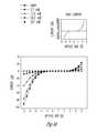
- FIG. 4 ashows the photocurrent in circles on the left axis and the internal quantum efficiency squares on the right axis are shown as a function of incident power at ⁇ 5 V bias;
- FIG. 4 bshows short circuit current (circles) and corresponding internal quantum efficiency (squares) as a function of incident power, the lines are provided to guide the eye, and the inset shows stability of the short circuit current as a function of time for a sample with much lower photovoltaic response than in FIG. 3 b ;
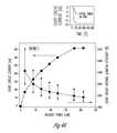
- FIG. 5shows photocurrent spectral responses and absorption spectra.
- Main PanelPhotocurrent spectral response (symbols) and the corresponding absorption spectra (solid line) for three different samples. The absorption peaks are tuned to 955 (black), 1200 (red), and 1355 nm (blue).
- InsetExtended spectral response for the sample centered at 955 nm, indicating the response in the region below ⁇ 600 nm where both the polymer and nanocrystal are excited. Also shown are the absorption spectra of the polymer and the nanocrystals.
- a three-dimensional bicontinuous heterostructure 10 produced in accordance with the present inventionincludes a substrate 12 having a first layer 14 made from constituent material A, a second layer 16 which constituents A and B are codeposited on top of first layer 14 in such a way as to obtain phase separation of the two constituents to form the second layer 16 .
- a third layer 18 comprised of constituent material B aloneis deposited onto layer second layer 16 .
- This structure shown in FIG. 1then comprises lower layer 14 of material A directly on the substrate 12 and the outer layer 18 of material B with the structure being characterized by layers A and B being highly interpenetrating at the interface between then which forms the second layer 16 .
- the two interpenetrating layersare spatially continuous (they consist only of protrusions (peninsulas) and no islands) and in which each layer forms the exclusive plane of contact to one side, one material to a bottom contact, the other material to a top contact.
- the thickness b 1is referred to as the lower buffer thickness and is the thickness of the layer 14 containing only material A.
- the thickness b 2is known as the upper buffer thickness and is the thickness of the layer 18 containing only material A.
- the thickness tis the thickness of the second layer 16 also known as the as the middle layer thickness.
- the dimension fis known as the average finger (or protrusion) height and is a measure of the interpenetration of constituent materials A and B.
- the dimension wis known as the average finger width.
- Thickness b 1is as thin as possible while still ensuring that the lower buffer is still entirely continuous (pinhole-free), typically from about 2 nm to about 200 nm.
- the thickness fis as thick as possible while still ensuring that each finger is continuous, preferably in a range from about 200 nm to about 20 um.
- the thickness tis greater than or equal to, but in any case very similar to, thickness f.
- the thickness b 2is as thin as possible while still ensuring that the upper buffer is still entirely continuous (pinhole-free), preferably in the range from about 2 to about 200 nm.
- the dimension wis between about 10 nm and 1000 nm, but preferably in the range from about 50 to about 200 nm.
- One method of producing the nanocomposite layered deviceincludes depositing the first material on a surface of a substrate to form a first continuous layer, and treating it to render it non-redispersable in a solvent.
- a dispersionif formed by co-dispersing the first material and the second material in the solvent and depositing the dispersion on a top surface of the first layer to form a second layer completely covering the first layer with the dispersion being deposited in such a way as to obtain phase separation of the first and second materials.
- the resulting layeris treated to render it non-redispersible in a solvent used to disperse the second material which is then deposited on the top surface of the second layer to form a third continuous layer completely covering the second layer.
- first layeris a continuous layer of the first material
- third layeris a continuous layer of the second material
- second layeris an interpenetrating interfacial layer between said first and second materials, formed by protrusions from the first and second materials which are spatially continuous.
- the nanocomposite layered devicemay be annealed after being produced.
- material Ais first dispersed in a first solvent and A is first deposited on substrate 12 to form a continuous, planar coating 14 , Coating 14 is treated to be non-redispersable in a second solvent. Materials A and B are co-dispersed in the second solvent and then A and B are co-deposited on top of layer 14 , forming layer 16 . Layer 16 is then treated to render it non-redispersible in a third solvent. Material B is dispersed in this third solvent and material B is deposited on layer 16 to produce layer 18 .
- the step of rendering layer 16 non-redispersiblemay be achieved in one of several ways including taking no action in which case the material will no longer disperse following evaporation of its solvent.
- Another wayuses a solution-phase treatment which involves the removal of a moiety, such as the ligands used to cap colloidal quantum dots, which served to provide solubility in that medium's original solvent so that the material will no longer disperse in the solvent.
- the treatmentmay involve submerging the structure in a new solvent, or spraying a new solvent on the structure, or spin-coating a new solvent onto the structure.
- Another wayuses a gas-phase treatment which involves exposing the structure to an environment rich in a particular gas, or alternatively lacking any gas (a vacuum environment), and exposing the structure to a particular temperature profile, generally involving a temperature elevated beyond room temperature.
- a gas-phase treatmentwhich involves exposing the structure to an environment rich in a particular gas, or alternatively lacking any gas (a vacuum environment), and exposing the structure to a particular temperature profile, generally involving a temperature elevated beyond room temperature.
- the materialwill no longer disperse due to the removal of a moiety, such as the ligands used to cap colloidal quantum dots, which served to provide solubility in that medium's original solvent.
- the solventsmay include for example chloroform, tolune, dichlorobenzene, hexanes, pyridine, water, N,N-dimethylformamide, acetone, methanol, isopropanol to mention just a few.
- the gasesmay include oxygen, argon, nitrogen, and reducing gas agents such as chlorine. Vacuum may also be used.
- FIGS. 1 and 2Another process to make the structure of FIGS. 1 and 2 includes forming an essentially planar continuous bottom layer of first material A on the substrate surface, forming a layer of first material A on top of the bottom layer which is textured to produce protrusions for subsequent interpenetration with second material B then coating second material B onto this structure and forming a final coating with second material B that ensures that only material B is contacted by subsequent layer.
- the nanocomposite layered devicemay be made by depositing the first material on the surface of the substrate to form a first continuous layer, and then texturing it to produce a textured layer material having protrusions.
- the second materialis then deposited onto the textured first material such that the second material interpenetrates the protrusions and completely covers the protrusions with a second continuous layer so that none of the protrusions of the first material are exposed.
- the step of depositing the material A on the surface of the substrateincludes depositing the material A to form a continuous layer then depositing more of the first material A under conditions suitable to give a textured layered having protrusions.
- the second material Bis deposited to fill in the textured layer having protrusions, and then depositing more of the second material B to give a continuous layer on top of interpenetrating interfacial layer.
- the first material A and the second material Bmay each to be chosen from the list including polymers, nanocrystals or quantum dots, conductive oxides, polymer-nanocrystal composite where the nanocrystals or quantum dots are preferably visible and/or infrared-absorbing semiconducting quantum dot nanoparticle composites. While each of materials A and B can be selected from the same list of materials they are not identical materials.
- the nanocomposite layered devicemay be made with a variety of infrared-absorbing semiconducting quantum dot nanoparticles made of materials including, but not limited to, Ge, Si, SiGe, PbS, CdS, CdSe, PbSe, InAs, InP, InSb and InGaAsP.
- Core-shell nanoparticlesconsisting of combinations of these or other semiconductors arrayed in a core-shell geometry may also be used incorporated into one the two materials.
- Material Amay include a semiconducting polymer underlayer
- material Bmay be a nanocomposite layer containing a semiconducting polymer in combination with the infrared-absorbing quantum dot nanoparticles deposited in such a way that the middle layer 16 is comprised of materials A and B being interpenetrated, not forming a uniform mixture.
- Material A in layer 14may be formed of just the above mentioned semiconductor nanoparticles, initially coated with organic ligands (amines, thiols, fatty acids, phosphines, phosphine oxides).
- Material Amay also include organic molecules, be they oligomeric or polymeric (MEH-PPV, polythiophene including regio-regular polythiophene) which transport electrons and/or holes.
- Material Amay also include conductive oxides including but not limited to indium tin oxide, tin oxide, antimony-doped indium tin oxide and antimony-doped tin oxide.
- Material Bmay be chosen from the same list of materials as used for material A. Specific combinations of material A and B of interest include: material A is an infrared light-absorbing material such as PbS quantum dots, or a blend of PbS quantum dots with another solution-processed material (e.g. MEH-PPV) resulting in material A being a nanocomposite; and Material B is a semiconducting polymer, or a conductive oxide, or another type of quantum dots such as PbSe, CdSe, or InP, or another blend of quantum dots with a semiconducting polymer. Variations are possible, for example constituents A and B may be interchanged between the first and third layers 14 and 18 respectively.
- material Ais an infrared light-absorbing material such as PbS quantum dots, or a blend of PbS quantum dots with another solution-processed material (e.g. MEH-PPV) resulting in material A being a nanocomposite
- MEH-PPVsolution-processed material
- compositions of material A and material Bmay include PbS quantum dot nanocrystals, chosen for their ability to absorb light at onset wavelengths tunable from ⁇ 800 nm to ⁇ 2000 nm 13 for photodetector and photovoltaic applications.
- the present inventionshows herein that a device's photocurrent spectrum corresponds to the nanocrystals' absorption spectrum, indicating that the sensitivity of the nanocomposite could potentially be tuned across the 800 to 2000 nm spectral region.
- the selection of the pair material A and material Bis important to achieving charge separation between the layers for photodetector and photovoltaic applications for example.
- Conjugated polymerstypically have better hole than electron mobility.
- photoconductivity in polymer/nanocrystal compositesrequires a band alignment that favors transfer of the photogenerated hole to the polymer; that is, the ionization potential of the polymer should, ideally, lie closer to vacuum than that of the nanocrystal.
- the bulk ionization potential of PbSis ⁇ 4.95 eV, while most conjugated polymers have ionization potentials greater than ⁇ 5.3 eV 14 .
- the low ionization potential of PbS relative to other semiconductor materials used in nanocrystal-based photoconductive devices such as the cadmium chalcogenideslimits the number of readily available conjugated polymers that provide a favorable energy alignment.
- MEH-PPVwas selected for its low ionization potential, variously reported between ⁇ 4.9 eV and ⁇ 5.1 eV 15,16 .
- MEH-PPV/PbSwould provide the type-II heterojunction needed for efficient photoconduction and for the observation of a photovoltaic effect: the vacuum-referenced band edge of the organic component is uncertain; it is possible that a dipole layer could be formed at the interface between materials, altering the effective band alignment; and the nanocrystal energy levels vary with size.
- MEH-PPVwas one available conjugated polymer candidate to provide the correct heterostructure for this application.
- an electron-hole pairor exciton
- the excitondrifts to the interface between the two materials making up the heterostructure; and the electron-hole pair is separated, with the hole remaining on one side of the heterostructure, and the electron now being on the other side of the heterostructure with the electron and hole thus separately diffusing towards their respective electrical contacts.
- the layered structure disclosed hereincan operate without external bias (a photovoltaic) as well as with external bias (a photodetector).
- the nanocomposite layered devicecan be produced using materials wherein the work functions of the materials are such that electrons travel towards one electrode contacting one material, and holes travel to the opposite electrode contacting the other material, resulting in a photovoltaic effect, i.e. the development of a sustained potential difference accompanied by net current flow into an external circuit without the application of an external bias.
- Either one of the materials, or both of the materialsmay comprise semiconductor quantum dots only, a composite of a polymer and quantum dots, a composite of quantum dots and organic molecules which transport electrons and/or holes, polymers, polymers or organics alone which are semiconducting and absorb in the spectral region of interest.
- the two materialswould not be made of identical materials, but if they are both made of quantum dots, they could be made of the same semiconducting material but would have different sizes of dots, or they could be made of quantum dots with different semiconducting materials. If one or both materials are made of semiconductor quantum dot nanoparticles alone, then organic materials such as organic ligands may be removed, for example as disclosed in copending U.S. Patent Application Ser. No. 60/170,944 Filed on Aug. 25, 2005.
- Preferred devices produced in accordance with the present inventionare comprised of a sandwich structure of glass, indium tin oxide (ITO), poly(p-phenylenevinylene) (PPV) (used as material A), a MEH-PPV/PbS nanocrystal blend (used as material B), and an upper Mg metal electrical contact.
- ITOindium tin oxide
- PPVpoly(p-phenylenevinylene)
- MEH-PPV/PbS nanocrystal blendused as material B
- an upper Mg metal electrical contactan upper Mg metal electrical contact
- the PPV layerprovides a number of improvements over samples with the MEH-PPV/nanocrystal layer deposited directly on the ITO: it provides better electrical stability by forming a smooth and pinhole-free pre-layer on which the blend films can be cast, eliminating catastrophic shorts from the upper contact directly through to the ITO; it decreases the dark current by introducing an injection barrier at the ITO contact, allowing larger photocurrent to dark current ratios; and it allows a higher bias to be applied to the samples before electrical breakdown, allowing the establishment of a higher internal field, more efficient photogenerated carrier extraction, and consequently higher photocurrents.
- the present inventionuses nanotechnology to make solution-processed materials “see in the dark”.
- the material of the present inventioncan be painted on pre-existing semiconductor substrates and chips, plastic substrates, printed on paper, or made into textiles.
- the devices produced hereinhave utility and numerous applications in producing photovoltaic devices which harvest the significant portion of the sun's spectral power that lies in the short-wavelength infrared.
- Other applicationsinclude the production of electroluminescent sources, photodetectors, and optical modulators.
- materials A and Bshould be one of the following combinations: 1) Polymer-nanocrystal, 2) conductive oxide-nanocrystal, 3) nanocrystal-nanocrystal (two different materials systems).
- a 170 nm thick polymer/nanocrystal blend filmwas spin-coated on to a 2.54 ⁇ 2.54 cm 2 indium tin oxide (ITO) coated glass slide. Films that were annealed were then heated on a hotplate at the designated temperatures for 1 hour in a N 2 -filled glove box with ⁇ 1 ppm residual oxygen and water. Finally, the upper contact (3 mm 2 ) was deposited by vacuum evaporation forming a metal stack of 30 nm Mg/100 nm Ag/5 nm Au.
- ITOindium tin oxide
- the dark current and photocurrentwere measured using an Agilent 4155C Semiconductor Parameter Analyzer and microprobe station.
- the optical excitationwas provided by a 970 nm semiconductor laser working in CW mode with the beam enlarged to a diameter of ⁇ 3 mm by a lens.
- no biaswas applied to the devices and the load resistor.
- the resistance of the series load resistorwas about three orders of magnitude smaller than the resistance of the device under illumination.
- the potential drop across the load resistorwas read by a lock-in amplifier (Model SR803 DSP) for the photocurrent spectral response and by a digital phosphor oscilloscope (Tektronix TDS5104) for the time response.
- the light from a white light sourcewas dispersed by a monochromater (Triax 320), and mechanically chopped at a frequency of 250 Hz.
- the light intensity at each wavelengthwas separately measured so the photocurrent at each wavelength could be scaled to the same incident light intensity by assuming the photocurrent was linearly proportional to the light power in the low intensity region used.
- Photoluminescence spectrawere obtained using a Photon Technologies Inc. spectrofluorometer with a Samples for thermal gravimetric analysis (TGA) were precipitated from chloroform solution, isolated by centrifugation, and dried in vacuum for several hours prior to analysis.
- TGAwas performed using a Cross-sectional TEM samples were prepared as follows: (1) a portion of the coated film was removed from the glass using a razor blade; (2) this film was glued onto a piece of plastic; (3) the plastic, with the sample attached, was microtomed to 70 nm thick species and mounted the species onto the TEM grids.
- the synthesisfollowed that used in Ref. 13.
- the as-prepared nanocrystalswere capped with oleic acid ligands.
- a post-synthesis ligand exchangewas performed to replace these with octylamine ligands.
- the original oleic acid-capped nanocrystalswere precipitated with methanol, dried, and dispersed in an excess of octylamine. This solution was heated at 70° C. for ⁇ 16 hours. After heating, the octylamine capped nanocrystals were precipitated with N,N-dimethylformamide and redispersed in chloroform.
- the nanocrystalswere then mixed with MEH-PPV to give a known weight fraction.
- a 40 nm polyp-phenylenevinylene) (PPV) hole transport layerwas spin-coated on 2.5 ⁇ 2.5 cm 2 indium tin oxide (ITO) coated glass slide and annealed at 200° C. for 3 hours in vacuum to allow polymerization.
- a MEH-PPV/nanocrystal blend(90% nanocrystal by weight of PbS nanocrystals to MEH-PPV) dissolved in chloroform was spin-coated on the PPV layer to form a film of thickness 100-150 nm.
- the upper contactwas deposited by vacuum evaporation forming a 3 mm 2 metal stack of 150 nm Mg/100 nm Ag/10 nm Au.
- 0 V biaswas applied to the sample connected in series with a load resistor of ⁇ 100 ⁇ , which was about three orders of magnitude smaller than the resistance of the sample. Illumination was provided by a white light source dispersed by a monochromator (Triax 320) and mechanically chopped at a frequency of ⁇ 250 Hz. Various filters were used to avoid overtones of the monochromator's grating from illuminating the sample. The potential drop across the load resistor was read by a lock-in amplifier (Model SR803 DSP). The light intensity at each wavelength was separately measured. Then, the photocurrent at each wavelength was scaled to the same incident light intensity by assuming that the photocurrent was linearly proportional to the light intensity in the low intensity region used.
- FIGS. 3 a and 3 bshow dark current and photocurrent versus applied bias at the ITO electrode for a nanocomposite photovoltaic device.
- the pump powersare shown in the figure legends.
- the datawere taken using an Agilent 4155C Semiconductor Parameter Analyzer and microprobe station.
- the optical excitationwas provided by a 975 nm continuous-wave semiconductor laser, which allowed selective excitation of the nanocrystal phase.
- the main panelshows dark current and photocurrent results for a sample with ⁇ 90% by weight nanocrystals in the polymer/nanocrystal blend.
- the insetshows the dark current for the main panel.
- the dark currentis 216 nA at a bias of 5 V and 144 nA at ⁇ 5 V (Inset FIG.
- the photo I-V curvesshow diode-like behaviour, with higher photocurrents in the reverse bias.
- the asymmetry of the photocurrent I-V curvescan be ascribed to the work function difference between ITO ( ⁇ 4.8 eV) and Mg (3.7 eV) and to the energy levels of the PPV layer.
- the photocurrentis 8.43 ⁇ A for 2.7 mW incident power and 90.61 ⁇ A for 207 mW incident power, which represents a ratio of photocurrent to dark current of 59 and 630, respectively.
- the above photocurrent under 2.7 mW illuminationrepresents a responsivity of 3.1 ⁇ 10 ⁇ 3 A/W.
- ITOis positively biased at 5 V
- the photocurrentis reduced to 5.39 and 28.12 ⁇ A for incident powers of 2.7 and 207 mW, respectively.
- FIG. 3 bthe main panel shows the dark current and photocurrent curves near zero bias, demonstrating the photovoltaic effect exhibited by this structure.
- the data for FIG. 3 bwere obtained from a different sample than shown in FIG. 3 a and represent the best results to date for short circuit current and open circuit voltage.
- FIG. 3 bshows a possible band diagram for the structure after the Mg contact has been deposited, and the device reaches the equilibrium state.
- the lowest energy absorption peakis assumed to be the first excitonic absorption of the PbS nanocrystals. This is used to estimate an increase in bandgap energy relative to bulk PbS, which has a bandgap of 0.41 eV; for the nanocrystals with absorption peaks centered at 955, 1200, and 1355 nm depicted in FIG. 3 , the effective bandgaps are 1.30, 1.03, and 0.92 eV, respectively.
- the barrier for electronscomes from the octylamine ligand, which passivates the nanocrystal surface, and/or the MEH-PPV (ionization energy ⁇ 4.9 eV and electron affinity ⁇ 2.9 eV 15 ), which surrounds the nanocrystal.
- the Mg sidetilts down and the ITO side tilts up.
- Similar band tilting in polymers and in C 60 doped polymers sandwiched between two different conductorshave been discussed by Greczynski et al 17 and Brabec et al 18 , respectively.
- the hole in the valence bandmay transfer to the hole conducting MEH-PPV, and the electron can either remain in the quantum dot or move through the nanocrystal network by hopping or tunnelling.
- the electron and holecan move towards the ITO or towards the Mg.
- FIG. 3 bshows dark and illuminated I-V curves for the region near 0 V, demonstrating the presence of a photovoltaic effect under continuous-wave illumination at 975 nm.
- the maximum short circuit currentis 350 nA for an incident power of 207 mW.
- the open circuit voltageis 0.36 V.
- the photovoltaic effectwas checked for hysteresis effects to see whether slow charge reorganization alone could be the cause.
- a sample demonstrating much lower short circuit current ( ⁇ 15 nA) than shown in FIG. 3 bwas used to provide more convincing evidence that, even with very low short circuit currents, the effect is not simply a hysteretic artefact.
- FIG. 4 ashows the photocurrent in circles on the left axis and the internal quantum efficiency squares on the right axis are shown as a function of incident power at ⁇ 5 V bias.
- the internal quantum efficiencyis defined as the ratio of the number of collected charges to the number of absorbed photons at the pump wavelength. The calculation of internal quantum efficiency using absorption values obtained in reflection mode, the handling of optical interference effects, and the range bars on these efficiency values are described in detail in the Methods section.
- FIG. 4 bshows short circuit current (circles) and corresponding internal quantum efficiency (squares) as a function of incident power. The lines are merely provided to guide the eye. Inset: Stability of the short circuit current as a function of time for a sample with much lower photovoltaic response than in FIG. 3 b.
- the percent absorption at the 975 nm wavelength used to obtain the main efficiency points in FIGS. 4 a and 4 bwas 12.7%; the upper and lower range bars represent upper and lower bounds obtained based on the consideration of multiple pass propagation through the active layer. From the figure it can be seen that the photocurrent does not increase linearly with incident power. Above ⁇ 50 mW, the photocurrent increases more slowly with increased power. In the low power region, the recombination of trapped electrons in the nanocrystal network with holes in the neighboring polymer dominates. When more photons are absorbed at higher powers, bimolecular recombination between free holes and electrons occurs in addition to the recombination at electron trap centers 8 .
- the additional bimolecular recombinationreduces the number of photo-excited carriers and, hence, lowers the internal quantum efficiency as shown in FIG. 4 a .
- the internal quantum efficiencyis about 3% (ie. external quantum efficiency of ⁇ 0.38%), while at 207 mW the internal quantum efficiency is reduced to about 0.4%.
- the short circuit current and corresponding internal quantum efficiencyis plotted in FIG. 4 b , showing a maximum value of ⁇ 0.006% (ie. short circuit external quantum efficiency of ⁇ 0.0008%).
- These zero bias internal quantum efficienciesare about 500 times lower than at ⁇ 5 V and show similar signs of a roll-off caused by bimolecular recombination at higher powers.
- the 3% internal quantum efficiency at ⁇ 5 Vis a three order-of-magnitude increase over that reported in Ref. 12 and is attributed principally to an improvement in film quality across these large-area devices.
- the MEH-PPV in previous workwas typically cast from toluene and was not ultra-sonicated or filtered.
- the MEH-PPVwas cast from chloroform, ultra-sonicated for 1 hour prior to casting the films, and both the polymer and nanocrystal solutions were independently filtered.
- the combination of the above treatmentswas shown using atomic force microscopy to provide smoother, more defect-free and pinhole-free films compared to the previous process.
- the improved surface of the films reported hereinallows better interfacial contact with the upper metal electrode resulting in better carrier extraction 21 .
- Films in the earlier workonly contained ⁇ 60% nanocrystal by weight because this was the maximum loading that gave films which did not suffer from excessive shorts.
- films containing 90% nanocrystal by weightwere successfully cast by optimizing the concentration, and hence viscosity, of both the nanocrystal and polymer solutions. The increased nanocrystal loading likely resulted in improved electron transport. Pinholes previously led in Ref.
- FIG. 5shows the absorbance spectrum of the nanocrystals (measured using a Varian CARY 500 Scan Spectrophotometer) used in three different devices, each tuned to a different part of the infrared spectrum, and the measured photocurrent spectral response of each device. No bias was applied to the devices during measurement of the photocurrent spectrum, and the excitation was provided by narrow wavelength bands selected from a white light source by a monochromator. At wavelengths longer than 600 nm, the absorption of MEH-PPV is negligible; thus, all absorption at these wavelengths is assigned solely to the PbS nanocrystals.
- the absorption peaks at 955, 1200, and 1355 nmcorrespond to the first excitonic absorption features in the three different choices of PbS nanocrystals.
- the photocurrent spectrashow peaks that match closely the absorption peaks associated with the nanocrystals. Along with demonstrating control over the spectral response, this result adds further evidence that the photocurrent is due to exciton formation in the nanocrystals followed by charge separation.
- the inset of FIG. 3shows the spectral response of the device with the 955 nm response peak, including shorter wavelengths where the polymer is also excited.
- the photocurrent responsepeaks at a wavelength 60 nm red-shifted relative to the polymer absorption peak.
- the active layeris a composite of the conjugated polymer MEH-PPV and PbS nanocrystals.
- the devicesshow a maximum photocurrent to dark current ratio of 630 at a bias of ⁇ 5 V.
- An internal quantum efficiency at ⁇ 5 V as high as 3%has been achieved.
- the devicesdemonstrate a photovoltaic response under 975 nm continuous-wave excitation where the maximum short circuit current was 350 nA and the open circuit voltage was 0.36 V.
- the maximum short circuit (photovoltaic) internal quantum efficiencywas 0.006%.
- the spectral response of the photocurrentclosely followed the absorption of the nanocrystals and was shown for three different regions of the infrared spectrum. The internal efficiencies, improved from previous work, will benefit from further improvements once refined control over the ligand barrier is obtained.
- the nanocomposite layerone means of making Material A or Material B, can be further improved using the methods described below. These methods resulted in a three-order-of-magnitude improvement in infrared photoconductive internal quantum efficiency compared to, allowing observation of the photocurrent under continuous-wave illumination without reliance on lock-in techniques; and also the first observation of an infrared photovoltaic effect in such materials.
- detectors of the present inventionshow an internal quantum efficiency of 3%, a ratio of photocurrent to dark current of 630, and a maximum responsivity of 3.1 ⁇ 10 ⁇ 3 A/W.
- the photovoltaic response under 975 nm excitationresults in a maximum open circuit voltage of 0.36 V, short circuit current of 350 nA, and short circuit internal quantum efficiency of 0.006%.
- the present inventionalso demonstrates, by varying the size of the nanocrystals during processing, photocurrent spectra with peaks tailored to 980 nm, 1.200 ⁇ m, and 1.355 ⁇ m.
- the present inventiontook the approach that thermal treatment of the nanocomposite films could result in dramatically enhanced hole transfer from PbS quantum dots to the polymer matrix by increasing the intimacy of contact between the inorganic and polymer phases, potentially via the displacement of some ligands contacting the nanocrystal surfaces, allowing portions of the polymer chains to interact with the nanocrystal surface without the ligand barrier present.
- a number of reports in the literaturehave investigated the effects of annealing on polymer-based photovoltaic systems, typically citing changes in film morphology as the cause for improved charge separation or charge mobility.
- the effect of annealing on bilayer or blend photovoltaicsis remarkable.
- all of the above studiesare related to solar cells working in the visible spectral region.
- No reportsare related to the influence of annealing on photovoltaics made from blends of organic and small band gap inorganic materials, which can be used in the infrared region.
- the present inventionshows herein, that thermal annealing of MEH-PPV/PbS nanocrystal films results in increased dark conductivity and a more rapid photoconductive response, as well as up to a 200-fold improvement in short-circuit current and 600-fold increase in maximum power output.
- the maximum monochromatic power conversion efficiency achieved upon annealingwas 0.001% under 16 mW illumination at 975 nm.
- the short circuit internal quantum efficiency of annealed samplesis about 0.15%, compared to 0.0064% for the best sample reported in Ref. 23. It is of scientific interest to study the role of the ligand and nanocrystal/polymer phase interaction on photovoltaic device performance. It is also of practical importance to achieve higher performance photovoltaic devices by replacing, in the solid state, the high and wide potential barriers for carriers posed by the organic ligand, especially when a ligand with a lower barrier, suitable for solution processing with the polymer, is not available.
- Ligand and film morphology controlhave a significant effect on the performance of PbS nanocrystal/MEH-PPV infrared-sensitive photovoltaic devices
- Annealingresults in displacement of octylamine ligands from the NC surface, allowing more intimate contact with the MEH-PPV phase, and thus improving the charge separation process.
- the quenching of the nanocrystal photoluminescence after annealingalso suggests rapid exciton dissociation before recombination Annealing also decreases the separation between isolated domains of nanocrystals within the network, enhancing the electron transport.
- Sensitizing conjugated polymers with infrared active nanocrystal quantum dotsprovides a spectrally tunable means of accessing the infrared while maintaining the advantageous properties of polymers.
- the present inventionuses such a nanocomposite approach in which quantum size effect-tuned PbS nanocrystals sensitize the conjugated polymer poly[2-methoxy-5-(2′-ethylhexyloxy-p-phenylenevinylene)] (MEH-PPV) into the infrared.
- the present inventionachieves, in a solution-processed device and with sensitivity far beyond 800 nm, harvesting of infrared-photogenerated carriers and the demonstration of an infrared photovoltaic effect.
- the present inventionalso exploits the wavelength tunability afforded by the nanocrystals to show photocurrent spectra tailored to three different regions of the infrared spectrum.
- the present inventiongenerally demonstrate, using solution-processed materials, both a three-order-of-magnitude improvement in infrared photoconductive internal quantum efficiency compared to, allowing observation of the photocurrent under continuous-wave illumination without reliance on lock-in techniques; and also the first observation of an infrared photovoltaic effect in such materials.
- detectors of the present inventionshow an internal quantum efficiency of 3%, a ratio of photocurrent to dark current of 630, and a maximum responsivity of 3.1 ⁇ 10 ⁇ 3 A/W.
- the photovoltaic response under 975 nm excitationresults in a maximum open circuit voltage of 0.36 V, short circuit 5 current of 350 nA, and short circuit internal quantum efficiency of 0.006%.
- the present inventionalso demonstrates, by varying the size of the nanocrystals during processing, photocurrent spectra with peaks tailored to 980 nm, 1.200 ⁇ m, and 1.355 ⁇ m.
- the terms “comprises” and “comprising”are to be construed as being inclusive and opened rather than exclusive. Specifically, when used in this specification including the claims, the terms “comprises” and “comprising” and variations thereof mean that the specified features, steps or components are included. The terms are not to be interpreted to exclude the presence of other features, steps or components.
Landscapes
- Engineering & Computer Science (AREA)
- Chemical & Material Sciences (AREA)
- Nanotechnology (AREA)
- Physics & Mathematics (AREA)
- Crystallography & Structural Chemistry (AREA)
- Electromagnetism (AREA)
- Mathematical Physics (AREA)
- Theoretical Computer Science (AREA)
- Inorganic Chemistry (AREA)
- Photovoltaic Devices (AREA)
- Light Receiving Elements (AREA)
Abstract
Description
- This patent application is a continuation of U.S. patent application Ser. No. 11/327,655, filed on Jan. 9, 2006, which relates to, and claims the priority benefit from, U.S. Provisional Patent Application Ser. No. 60/641,766, filed on Jan. 7, 2005, entitled “QUANTUM DOT—POLYMER NANOCOMPOSITE PHOTODETECTORS AND PHOTOVOL TAICS,” both of which are incorporated herein in their entireties.
- The present invention relates to a three-dimensional bicontinuous heterostructure, a method of producing same, and the application of this structure towards the realization of photodetecting and photovoltaic devices working in the visible and the near-infrared.
- In contrast to traditional semiconductors, conjugated polymers provide ease of processing, low cost, physical flexibility, and large-area coverage. These active optoelectronic materials produce and harvest light efficiently in the visible spectrum. The same functions are required in the short-wavelength infrared (1-2 um) for telecommunications (1300-1600 nm), nightime and low-light imaging (1000 nm and beyond), biological imaging (800 nm and 1100 nm and 1300 nm transparent tissue windows), thermal photovoltaics (>1900 nm), and solar cells (800-2000 nm). Photodetecting and photovoltaic polymer devices have yet to demonstrate significant sensitivity beyond ˜800 nm.
- Organic/nanocrystal composites have been demonstrated to enable a number of important optoelectronic devices operating in the visible region. In the infrared, electroluminescence has been demonstrated from such materials. Prior to the results presented herein, there has been no demonstration of a short-wavelength infrared photovoltaic effect from such a material system.
- Control of organic-inorganic interfaces on the nanoscale is of critical importance in organic electronics, and in particular in photovoltaic devices based on inorganic quantum dots embedded in a semiconducting polymer matrix. In these systems, rapid and efficient charge separation is needed for subsequent separate transport and extraction of electrons and holes. Organic ligands passivating the surfaces of nanocrystals are needed to enable solution-processing without aggregation, yet these ligands are typically insulating and thus impede charge transfer between the nanocrystal and polymer. Moderate success has been achieved in conjugated polymer/inorganic nanocrystal composite-based solar cells active in the visible region, and these hold the promise for fabrication of large area photovoltaics on flexible substrates using low-cost processing methods such as solution spin coating. However, approximately 50% of solar energy reaching the Earth's surface lies in the visible region, and the remainder in the infrared (IR) region beyond 700 nm. It is therefore of great interest to develop IR sensitive devices, ultimately to enable harvesting of the full solar spectrum.
- Infrared photoconductive and photovoltaic devices based on the solution-processible PbS quantum dot/MEH-PPV materials system have recently been reported. These first reports exhibited promising efficiencies meriting further optimization. Many factors can affect photovoltaic device performance, such as the effectiveness of charge separation and the magnitude of charge mobility, as well as the efficiency of charge collection. It is fundamentally important to understand these processes and to increase the effectiveness of these processes in the device in order to optimize performance.
- The present invention consists of a three-dimensional bicontinuous heterostructure, a method of producing same, and the application of this structure towards the realization of photodetecting and photovoltaic devices working in the visible and the near-infrared.
- In one aspect of the invention there is provided a nanocomposite layered device, comprising:
- a) a three-dimensional bicontinuous heterostructure including at least two materials with a first material formed on a substrate, a second material located on the first material, said first and second materials each having a structure and morphology which includes protrusions and wherein said protrusions from said first material penetrate into said second material and said protrusions from said second material penetrate into said first material to form an interpenetrating interface between said first and second materials, and wherein said protrusions from said first and second materials are spatially continuous;
- b) wherein said first material and said second material are selected from the group consisting of polymers, visible and/or infrared-absorbing semiconducting quantum dot nanoparticles, conductive oxides and polymer-visible and/or infrared-absorbing semiconducting quantum dot nanoparticle composites but are not identical materials, and
- c) wherein upon absorption of light in said first or second material an electron-hole pair is formed which drifts to said interpenetrating interface wherein said the electron-hole pair is separated with the hole moving into one of the materials and the electron moving into the other material.
- In another aspect of the invention there is provided a nanocomposite layered device, comprising:
- A nanocomposite layered device, comprising:
- a) a three-dimensional bicontinuous heterostructure including at least two materials with a first material formed on a substrate, a second material located on the first material, said first and second materials each having a structure and morphology which includes protrusions and wherein said protrusions from said first material penetrate into said second material and said protrusions from said second material penetrate into said first material to form an interpenetrating interface between said first and second materials, and wherein said protrusions from said first and second materials are spatially continuous;
- b) at least of one of said first and second materials includes visible and/or infrared-absorbing semiconducting quantum dot nanoparticles; and
- c) wherein upon absorption of light by said visible and/or infrared-absorbing quantum dot nanoparticles, an electron-hole pair is formed which drifts to said interpenetrating interface wherein said the electron-hole pair is separated.
- The three-dimensional bicontinuous heterostructure is a composition of matter in which at least two interpenetrating layers are spatially continuous (they are comprised only of peninsulas, and no islands); and in which each layer forms the exclusive plane of contact to one side, one material to a bottom contact, the other material to a top contact.
- The method of producing the three-dimensional bicontinuous heterostructure relies on forming an essentially planar continuous bottom layer of a first material; forming a layer of this first material on top of the bottom layer which is textured to produce protrusions for subsequent interpenetration with a second material, coating this second material onto this structure; and forming a final coating with the second material that ensures that only the second material is contacted by subsequent layer.
- Thus in one aspect of the present invention there is provided a process for producing a nanocomposite layered device, comprising the steps of:
- a) depositing a first material on a surface of a substrate to form a first continuous layer, and treating said first continuous layer to render it non-redispersable in a first solvent;
- b) forming a first dispersion by co-dispersing said first material and a second material in said first solvent and depositing said first dispersion on a top surface of said first layer to form a second layer completely covering said first layer of pre-selected thickness in such a way as to obtain phase separation of the first and second materials constituents and treating said second layer to render it non-redispersible in a second solvent;
- c) forming a dispersion by dispersing said second material in said second solvent and depositing it on a top surface of said second layer to form a third continuous layer completely covering said second layer;
- d) wherein a structure formed in steps a), b) and c) is a three-dimensional bicontinuous heterostructure wherein said first layer is a continuous layer of said first material, said third layer is a continuous layer of said second material and said second layer is an interpenetrating interfacial layer between said first and second materials, formed by protrusions from said first and second materials which are spatially continuous; and
- e) wherein at least one of said first and second materials includes visible and/or infrared-absorbing semiconducting quantum dot nanoparticles, and wherein at least one of said first and second materials includes an electron conducting constituent and the other material includes a hole conducting constituent.
- The nanocomposite layered device may be annealed after being produced.
- In another aspect a process for producing a nanocomposite layered device comprises the steps of:
- a) depositing a first material on a surface of a substrate to form a first continuous layer, and texturing said first continuous layer treating said first continuous layer to produce a textured first material having protrusions;
- b) depositing a second material onto the textured first material having protrusions such that the second material interpenetrates said protrusions and completely covers the protrusions with a second continuous layer so that none of the protrusions of the first material are exposed;
- c) wherein a structure formed in steps a) and b) is a three-dimensional bicontinuous heterostructure including first continuous layer of said first material, a third continuous layer of said second material and said second layer is an interpenetrating interfacial layer between said first and second materials, formed by protrusions from said first and second materials which are spatially continuous; and
- d) wherein at least one of said first and second materials includes visible and/or infrared-absorbing semiconducting quantum dot nanoparticles, and wherein at least one of said first and second materials includes an electron conducting constituent and the other material includes a hole conducting constituent.
- These methods are all reliant upon means described herein of ensuring that the deposition of progressive layers, typically using solution-processing, does not result in redispersion of the layer or layers lying beneath. This relies on a variety of treatments to the underlying layers that ensure non-redispersion in ensuing layers' solvents used in deposition.
- Further features of the invention will be described or will become apparent in the course of the following detailed description.
- The invention will now be described by way of example only, with reference to the accompanying drawings, in which:
FIG. 1 shows a cross section of a three-dimensional bicontinuous heterostructure produced in accordance with the present invention;FIG. 2 is the same asFIG. 1 but showing the labelled dimensions for thickness, width of the three-dimensional bicontinuous heterostructure;FIG. 3 ashows dark current and photocurrent versus applied bias at the ITO electrode for a three-dimensional bicontinuous heterostructure shown inFIG. 1 over a wide potential range from −5V to +5V;FIG. 3 bshows dark current and photocurrent curves in the vicinity of zero bias, of a sample different to the sample ofFIG. 3 a, demonstrating the photovoltaic effect;FIG. 4 ashows the photocurrent in circles on the left axis and the internal quantum efficiency squares on the right axis are shown as a function of incident power at −5 V bias;FIG. 4 bshows short circuit current (circles) and corresponding internal quantum efficiency (squares) as a function of incident power, the lines are provided to guide the eye, and the inset shows stability of the short circuit current as a function of time for a sample with much lower photovoltaic response than inFIG. 3 b; andFIG. 5 shows photocurrent spectral responses and absorption spectra. Main Panel: Photocurrent spectral response (symbols) and the corresponding absorption spectra (solid line) for three different samples. The absorption peaks are tuned to 955 (black), 1200 (red), and 1355 nm (blue). Inset: Extended spectral response for the sample centered at 955 nm, indicating the response in the region below ˜600 nm where both the polymer and nanocrystal are excited. Also shown are the absorption spectra of the polymer and the nanocrystals.- Referring to
FIG. 1 , a three-dimensional bicontinuous heterostructure10 produced in accordance with the present invention includes asubstrate 12 having afirst layer 14 made from constituent material A, asecond layer 16 which constituents A and B are codeposited on top offirst layer 14 in such a way as to obtain phase separation of the two constituents to form thesecond layer 16. Athird layer 18 comprised of constituent material B alone is deposited onto layersecond layer 16. This structure shown inFIG. 1 then compriseslower layer 14 of material A directly on thesubstrate 12 and theouter layer 18 of material B with the structure being characterized by layers A and B being highly interpenetrating at the interface between then which forms thesecond layer 16. The two interpenetrating layers are spatially continuous (they consist only of protrusions (peninsulas) and no islands) and in which each layer forms the exclusive plane of contact to one side, one material to a bottom contact, the other material to a top contact. - Referring to
FIG. 2 , the relative thicknesses of thefirst layer 14,second layer 16 andthird layer 18 are shown. The thickness b1 is referred to as the lower buffer thickness and is the thickness of thelayer 14 containing only material A. The thickness b2 is known as the upper buffer thickness and is the thickness of thelayer 18 containing only material A. The thickness t is the thickness of thesecond layer 16 also known as the as the middle layer thickness. The dimension f is known as the average finger (or protrusion) height and is a measure of the interpenetration of constituent materials A and B. The dimension w is known as the average finger width. - Thickness b1 is as thin as possible while still ensuring that the lower buffer is still entirely continuous (pinhole-free), typically from about 2 nm to about 200 nm. The thickness f is as thick as possible while still ensuring that each finger is continuous, preferably in a range from about 200 nm to about 20 um. The thickness t is greater than or equal to, but in any case very similar to, thickness f. The thickness b2 is as thin as possible while still ensuring that the upper buffer is still entirely continuous (pinhole-free), preferably in the range from about 2 to about 200 nm. The dimension w is between about 10 nm and 1000 nm, but preferably in the range from about 50 to about 200 nm.
- One method of producing the nanocomposite layered device includes depositing the first material on a surface of a substrate to form a first continuous layer, and treating it to render it non-redispersable in a solvent. A dispersion if formed by co-dispersing the first material and the second material in the solvent and depositing the dispersion on a top surface of the first layer to form a second layer completely covering the first layer with the dispersion being deposited in such a way as to obtain phase separation of the first and second materials. The resulting layer is treated to render it non-redispersible in a solvent used to disperse the second material which is then deposited on the top surface of the second layer to form a third continuous layer completely covering the second layer. This produces a three-dimensional bicontinuous heterostructure wherein the first layer is a continuous layer of the first material, the third layer is a continuous layer of the second material and the second layer is an interpenetrating interfacial layer between said first and second materials, formed by protrusions from the first and second materials which are spatially continuous.
- The nanocomposite layered device may be annealed after being produced.
- In one process to make the structure of
FIGS. 1 and 2 , material A is first dispersed in a first solvent and A is first deposited onsubstrate 12 to form a continuous,planar coating 14,Coating 14 is treated to be non-redispersable in a second solvent. Materials A and B are co-dispersed in the second solvent and then A and B are co-deposited on top oflayer 14, forminglayer 16.Layer 16 is then treated to render it non-redispersible in a third solvent. Material B is dispersed in this third solvent and material B is deposited onlayer 16 to producelayer 18. - The step of
rendering layer 16 non-redispersible may be achieved in one of several ways including taking no action in which case the material will no longer disperse following evaporation of its solvent. Another way uses a solution-phase treatment which involves the removal of a moiety, such as the ligands used to cap colloidal quantum dots, which served to provide solubility in that medium's original solvent so that the material will no longer disperse in the solvent. The treatment may involve submerging the structure in a new solvent, or spraying a new solvent on the structure, or spin-coating a new solvent onto the structure. Another way uses a gas-phase treatment which involves exposing the structure to an environment rich in a particular gas, or alternatively lacking any gas (a vacuum environment), and exposing the structure to a particular temperature profile, generally involving a temperature elevated beyond room temperature. The material will no longer disperse due to the removal of a moiety, such as the ligands used to cap colloidal quantum dots, which served to provide solubility in that medium's original solvent. - The solvents may include for example chloroform, tolune, dichlorobenzene, hexanes, pyridine, water, N,N-dimethylformamide, acetone, methanol, isopropanol to mention just a few. The gases may include oxygen, argon, nitrogen, and reducing gas agents such as chlorine. Vacuum may also be used.
- Another process to make the structure of
FIGS. 1 and 2 includes forming an essentially planar continuous bottom layer of first material A on the substrate surface, forming a layer of first material A on top of the bottom layer which is textured to produce protrusions for subsequent interpenetration with second material B then coating second material B onto this structure and forming a final coating with second material B that ensures that only material B is contacted by subsequent layer. - The nanocomposite layered device may be made by depositing the first material on the surface of the substrate to form a first continuous layer, and then texturing it to produce a textured layer material having protrusions. The second material is then deposited onto the textured first material such that the second material interpenetrates the protrusions and completely covers the protrusions with a second continuous layer so that none of the protrusions of the first material are exposed.
- In a variation of this method, the step of depositing the material A on the surface of the substrate includes depositing the material A to form a continuous layer then depositing more of the first material A under conditions suitable to give a textured layered having protrusions. The second material B is deposited to fill in the textured layer having protrusions, and then depositing more of the second material B to give a continuous layer on top of interpenetrating interfacial layer.
- The first material A and the second material B may each to be chosen from the list including polymers, nanocrystals or quantum dots, conductive oxides, polymer-nanocrystal composite where the nanocrystals or quantum dots are preferably visible and/or infrared-absorbing semiconducting quantum dot nanoparticle composites. While each of materials A and B can be selected from the same list of materials they are not identical materials.
- Those skilled in the art will understand that the nanocomposite layered device may be made with a variety of infrared-absorbing semiconducting quantum dot nanoparticles made of materials including, but not limited to, Ge, Si, SiGe, PbS, CdS, CdSe, PbSe, InAs, InP, InSb and InGaAsP. Core-shell nanoparticles consisting of combinations of these or other semiconductors arrayed in a core-shell geometry may also be used incorporated into one the two materials.
- Material A may include a semiconducting polymer underlayer, material B may be a nanocomposite layer containing a semiconducting polymer in combination with the infrared-absorbing quantum dot nanoparticles deposited in such a way that the
middle layer 16 is comprised of materials A and B being interpenetrated, not forming a uniform mixture. - Material A in
layer 14 may be formed of just the above mentioned semiconductor nanoparticles, initially coated with organic ligands (amines, thiols, fatty acids, phosphines, phosphine oxides). Material A may also include organic molecules, be they oligomeric or polymeric (MEH-PPV, polythiophene including regio-regular polythiophene) which transport electrons and/or holes. Material A may also include conductive oxides including but not limited to indium tin oxide, tin oxide, antimony-doped indium tin oxide and antimony-doped tin oxide. - Material B may be chosen from the same list of materials as used for material A. Specific combinations of material A and B of interest include: material A is an infrared light-absorbing material such as PbS quantum dots, or a blend of PbS quantum dots with another solution-processed material (e.g. MEH-PPV) resulting in material A being a nanocomposite; and Material B is a semiconducting polymer, or a conductive oxide, or another type of quantum dots such as PbSe, CdSe, or InP, or another blend of quantum dots with a semiconducting polymer. Variations are possible, for example constituents A and B may be interchanged between the first and
third layers - In preferred and useful compositions of material A and material B may include PbS quantum dot nanocrystals, chosen for their ability to absorb light at onset wavelengths tunable from ˜800 nm to ˜2000 nm13for photodetector and photovoltaic applications. The present invention shows herein that a device's photocurrent spectrum corresponds to the nanocrystals' absorption spectrum, indicating that the sensitivity of the nanocomposite could potentially be tuned across the 800 to 2000 nm spectral region.
- The selection of the pair material A and material B is important to achieving charge separation between the layers for photodetector and photovoltaic applications for example. Conjugated polymers typically have better hole than electron mobility. Thus, photoconductivity in polymer/nanocrystal composites requires a band alignment that favors transfer of the photogenerated hole to the polymer; that is, the ionization potential of the polymer should, ideally, lie closer to vacuum than that of the nanocrystal. The bulk ionization potential of PbS is ˜4.95 eV, while most conjugated polymers have ionization potentials greater than ˜5.3 eV14. The low ionization potential of PbS relative to other semiconductor materials used in nanocrystal-based photoconductive devices such as the cadmium chalcogenides (bulk ionization potentials between ˜6.4 eV and ˜7.3 eV) limits the number of readily available conjugated polymers that provide a favorable energy alignment. MEH-PPV was selected for its low ionization potential, variously reported between ˜4.9 eV and ˜5.1 eV15,16. It was not obvious at the outset that MEH-PPV/PbS would provide the type-II heterojunction needed for efficient photoconduction and for the observation of a photovoltaic effect: the vacuum-referenced band edge of the organic component is uncertain; it is possible that a dipole layer could be formed at the interface between materials, altering the effective band alignment; and the nanocrystal energy levels vary with size. However, MEH-PPV was one available conjugated polymer candidate to provide the correct heterostructure for this application.
- Under illumination, an electron-hole pair, or exciton, is formed and the exciton drifts to the interface between the two materials making up the heterostructure; and the electron-hole pair is separated, with the hole remaining on one side of the heterostructure, and the electron now being on the other side of the heterostructure with the electron and hole thus separately diffusing towards their respective electrical contacts.
- It will be understood that the layered structure disclosed herein can operate without external bias (a photovoltaic) as well as with external bias (a photodetector). For example, the nanocomposite layered device can be produced using materials wherein the work functions of the materials are such that electrons travel towards one electrode contacting one material, and holes travel to the opposite electrode contacting the other material, resulting in a photovoltaic effect, i.e. the development of a sustained potential difference accompanied by net current flow into an external circuit without the application of an external bias.
- Either one of the materials, or both of the materials, may comprise semiconductor quantum dots only, a composite of a polymer and quantum dots, a composite of quantum dots and organic molecules which transport electrons and/or holes, polymers, polymers or organics alone which are semiconducting and absorb in the spectral region of interest.
- The two materials would not be made of identical materials, but if they are both made of quantum dots, they could be made of the same semiconducting material but would have different sizes of dots, or they could be made of quantum dots with different semiconducting materials. If one or both materials are made of semiconductor quantum dot nanoparticles alone, then organic materials such as organic ligands may be removed, for example as disclosed in copending U.S. Patent Application Ser. No. 60/170,944 Filed on Aug. 25, 2005.
- Preferred devices produced in accordance with the present invention are comprised of a sandwich structure of glass, indium tin oxide (ITO), poly(p-phenylenevinylene) (PPV) (used as material A), a MEH-PPV/PbS nanocrystal blend (used as material B), and an upper Mg metal electrical contact. In addition to acting as a hole transport layer, the PPV layer provides a number of improvements over samples with the MEH-PPV/nanocrystal layer deposited directly on the ITO: it provides better electrical stability by forming a smooth and pinhole-free pre-layer on which the blend films can be cast, eliminating catastrophic shorts from the upper contact directly through to the ITO; it decreases the dark current by introducing an injection barrier at the ITO contact, allowing larger photocurrent to dark current ratios; and it allows a higher bias to be applied to the samples before electrical breakdown, allowing the establishment of a higher internal field, more efficient photogenerated carrier extraction, and consequently higher photocurrents.
- The present invention uses nanotechnology to make solution-processed materials “see in the dark”. The material of the present invention can be painted on pre-existing semiconductor substrates and chips, plastic substrates, printed on paper, or made into textiles.
- The devices produced herein have utility and numerous applications in producing photovoltaic devices which harvest the significant portion of the sun's spectral power that lies in the short-wavelength infrared. Other applications include the production of electroluminescent sources, photodetectors, and optical modulators. In the case of photodetectors, materials A and B should be one of the following combinations: 1) Polymer-nanocrystal, 2) conductive oxide-nanocrystal, 3) nanocrystal-nanocrystal (two different materials systems).
- The present invention will now be illustrated using the following non-limiting examples, which those skilled in the art will appreciate are meant to be exemplary only and in no way are meant to limit the scope of the invention.
- The synthesis of oleate-capped PbS nanocrystals followed that used in Ref. 13. These nanocrystals were then treated with octylamine in a ligand exchange procedure reported elsewhere. After the exhange process, the octylamine-capped nanocrystals were precipitated with N,N-dimethylformamide and redispersed in chloroform. The nanocrystal solutions were filtered using a 0.45 μm filter. MEH-PPV was dispersed in chloroform by stirring overnight followed by two hours of ultrasonication and filtration through a 2 μm filter. The nanocrystal and polymer solutions were then mixed to give an 80% weight fraction of nanocrystals relative to MEH-PPV.
- In a typical procedure, a 170 nm thick polymer/nanocrystal blend film was spin-coated on to a 2.54×2.54 cm2indium tin oxide (ITO) coated glass slide. Films that were annealed were then heated on a hotplate at the designated temperatures for 1 hour in a N2-filled glove box with <1 ppm residual oxygen and water. Finally, the upper contact (3 mm2) was deposited by vacuum evaporation forming a metal stack of 30 nm Mg/100 nm Ag/5 nm Au.
- The dark current and photocurrent were measured using an Agilent 4155C Semiconductor Parameter Analyzer and microprobe station. The optical excitation was provided by a 970 nm semiconductor laser working in CW mode with the beam enlarged to a diameter of ˜3 mm by a lens. In the measurement of photocurrent spectral response and time response, no bias was applied to the devices and the load resistor. The resistance of the series load resistor was about three orders of magnitude smaller than the resistance of the device under illumination. The potential drop across the load resistor was read by a lock-in amplifier (Model SR803 DSP) for the photocurrent spectral response and by a digital phosphor oscilloscope (Tektronix TDS5104) for the time response. To obtain the photocurrent spectrum, the light from a white light source was dispersed by a monochromater (Triax 320), and mechanically chopped at a frequency of 250 Hz. The light intensity at each wavelength was separately measured so the photocurrent at each wavelength could be scaled to the same incident light intensity by assuming the photocurrent was linearly proportional to the light power in the low intensity region used. Photoluminescence spectra were obtained using a Photon Technologies Inc. spectrofluorometer with a Samples for thermal gravimetric analysis (TGA) were precipitated from chloroform solution, isolated by centrifugation, and dried in vacuum for several hours prior to analysis. TGA was performed using a Cross-sectional TEM samples were prepared as follows: (1) a portion of the coated film was removed from the glass using a razor blade; (2) this film was glued onto a piece of plastic; (3) the plastic, with the sample attached, was microtomed to 70 nm thick species and mounted the species onto the TEM grids.
- The synthesis followed that used in Ref. 13. The as-prepared nanocrystals were capped with oleic acid ligands. A post-synthesis ligand exchange was performed to replace these with octylamine ligands. The original oleic acid-capped nanocrystals were precipitated with methanol, dried, and dispersed in an excess of octylamine. This solution was heated at 70° C. for ˜16 hours. After heating, the octylamine capped nanocrystals were precipitated with N,N-dimethylformamide and redispersed in chloroform. The nanocrystals were then mixed with MEH-PPV to give a known weight fraction.
- A 40 nm polyp-phenylenevinylene) (PPV) hole transport layer was spin-coated on 2.5×2.5 cm2indium tin oxide (ITO) coated glass slide and annealed at 200° C. for 3 hours in vacuum to allow polymerization. A MEH-PPV/nanocrystal blend (90% nanocrystal by weight of PbS nanocrystals to MEH-PPV) dissolved in chloroform was spin-coated on the PPV layer to form a film of thickness 100-150 nm. Finally, the upper contact was deposited by vacuum evaporation forming a 3 mm2metal stack of 150 nm Mg/100 nm Ag/10 nm Au.
- 0 V bias was applied to the sample connected in series with a load resistor of ˜100Ω, which was about three orders of magnitude smaller than the resistance of the sample. Illumination was provided by a white light source dispersed by a monochromator (Triax 320) and mechanically chopped at a frequency of ˜250 Hz. Various filters were used to avoid overtones of the monochromator's grating from illuminating the sample. The potential drop across the load resistor was read by a lock-in amplifier (Model SR803 DSP). The light intensity at each wavelength was separately measured. Then, the photocurrent at each wavelength was scaled to the same incident light intensity by assuming that the photocurrent was linearly proportional to the light intensity in the low intensity region used.
FIGS. 3 aand3bshow dark current and photocurrent versus applied bias at the ITO electrode for a nanocomposite photovoltaic device. The pump powers are shown in the figure legends. The data were taken using an Agilent 4155C Semiconductor Parameter Analyzer and microprobe station. The optical excitation was provided by a 975 nm continuous-wave semiconductor laser, which allowed selective excitation of the nanocrystal phase. The main panel shows dark current and photocurrent results for a sample with ˜90% by weight nanocrystals in the polymer/nanocrystal blend. The inset shows the dark current for the main panel. The dark current is 216 nA at a bias of 5 V and 144 nA at −5 V (InsetFIG. 3 a). The photo I-V curves show diode-like behaviour, with higher photocurrents in the reverse bias. The asymmetry of the photocurrent I-V curves can be ascribed to the work function difference between ITO (˜4.8 eV) and Mg (3.7 eV) and to the energy levels of the PPV layer. At a bias of −5 V, the photocurrent is 8.43 μA for 2.7 mW incident power and 90.61 μA for 207 mW incident power, which represents a ratio of photocurrent to dark current of 59 and 630, respectively. The above photocurrent under 2.7 mW illumination represents a responsivity of 3.1×10⁻³A/W. When ITO is positively biased at 5 V, the photocurrent is reduced to 5.39 and 28.12 μA for incident powers of 2.7 and 207 mW, respectively.- In
FIG. 3 b, the main panel shows the dark current and photocurrent curves near zero bias, demonstrating the photovoltaic effect exhibited by this structure. The data forFIG. 3 bwere obtained from a different sample than shown inFIG. 3 aand represent the best results to date for short circuit current and open circuit voltage. - The inset of
FIG. 3 bshows a possible band diagram for the structure after the Mg contact has been deposited, and the device reaches the equilibrium state. For this diagram, the lowest energy absorption peak is assumed to be the first excitonic absorption of the PbS nanocrystals. This is used to estimate an increase in bandgap energy relative to bulk PbS, which has a bandgap of 0.41 eV; for the nanocrystals with absorption peaks centered at 955, 1200, and 1355 nm depicted inFIG. 3 , the effective bandgaps are 1.30, 1.03, and 0.92 eV, respectively. Because of the nearly equal effective masses for holes and electrons in PbS, it is also assumed that the confinement energy is shared equally in the conduction and valence bands so the bands move up and down, respectively, by equal energies. The barrier for electrons comes from the octylamine ligand, which passivates the nanocrystal surface, and/or the MEH-PPV (ionization energy ˜4.9 eV and electron affinity ˜2.9 eV15), which surrounds the nanocrystal. - To align the Fermi level in all layers, the Mg side tilts down and the ITO side tilts up. (Similar band tilting in polymers and in C60doped polymers sandwiched between two different conductors have been discussed by Greczynski et al17and Brabec et al18, respectively). After an electron in the valence band of the nanocrystal is transferred to the conduction band by absorbing a photon, the hole in the valence band may transfer to the hole conducting MEH-PPV, and the electron can either remain in the quantum dot or move through the nanocrystal network by hopping or tunnelling. Depending on the polarity of the built-in and/or applied field, the electron and hole can move towards the ITO or towards the Mg. When the electron moves to the ITO side, it will see a higher barrier by the tilted band and PPV (ionization energy ˜5.1 eV and electronic affinity ˜2.7 eV19) than when moving to the Mg electrode. When the hole moves to the ITO, it also faces a barrier between MEH-PPV and PPV, and no barrier if it moves to the Mg side. Reverse bias results in photogenerated holes being extracted through the ITO/PPV side of the sample, while forward bias results in electrons being extracted through that side. Thus, the higher photocurrent in the reverse bias suggests that the electron barrier posed by the PPV may be more severe than the hole barrier in carrier extraction.
FIG. 3 bshows dark and illuminated I-V curves for the region near 0 V, demonstrating the presence of a photovoltaic effect under continuous-wave illumination at 975 nm. The maximum short circuit current is 350 nA for an incident power of 207 mW. The open circuit voltage is 0.36 V. The photovoltaic effect was checked for hysteresis effects to see whether slow charge reorganization alone could be the cause. A sample demonstrating much lower short circuit current (˜15 nA) than shown inFIG. 3 bwas used to provide more convincing evidence that, even with very low short circuit currents, the effect is not simply a hysteretic artefact. The inset ofFIG. 2 bshows the result of this test where the sample was held at zero bias and the short circuit current monitored over 500 seconds: the signal was stable over this time span. Further evidence that the effect was not hysteresis-based was provided by performing voltage scans in both directions (forward bias to reverse bias and vice versa); the direction of scan had negligible effect on the photovoltaic response. Although this photovoltaic response, which allows separation of an electron-hole pair at zero applied bias, could be indicative of a type-II heterostructure between the PbS nanocrystals and MEH-PPV, the built-in field in the device under zero bias is significant and could also allow charge separation with a marginal type-I heterostructure.FIG. 4 ashows the photocurrent in circles on the left axis and the internal quantum efficiency squares on the right axis are shown as a function of incident power at −5 V bias. The internal quantum efficiency is defined as the ratio of the number of collected charges to the number of absorbed photons at the pump wavelength. The calculation of internal quantum efficiency using absorption values obtained in reflection mode, the handling of optical interference effects, and the range bars on these efficiency values are described in detail in the Methods section.FIG. 4 bshows short circuit current (circles) and corresponding internal quantum efficiency (squares) as a function of incident power. The lines are merely provided to guide the eye. Inset: Stability of the short circuit current as a function of time for a sample with much lower photovoltaic response than inFIG. 3 b.- The percent absorption at the 975 nm wavelength used to obtain the main efficiency points in
FIGS. 4 aand4bwas 12.7%; the upper and lower range bars represent upper and lower bounds obtained based on the consideration of multiple pass propagation through the active layer. From the figure it can be seen that the photocurrent does not increase linearly with incident power. Above ˜50 mW, the photocurrent increases more slowly with increased power. In the low power region, the recombination of trapped electrons in the nanocrystal network with holes in the neighboring polymer dominates. When more photons are absorbed at higher powers, bimolecular recombination between free holes and electrons occurs in addition to the recombination at electron trap centers8. The additional bimolecular recombination reduces the number of photo-excited carriers and, hence, lowers the internal quantum efficiency as shown inFIG. 4 a. At an incident power of 2.7 mW the internal quantum efficiency is about 3% (ie. external quantum efficiency of ˜0.38%), while at 207 mW the internal quantum efficiency is reduced to about 0.4%. The short circuit current and corresponding internal quantum efficiency is plotted inFIG. 4 b, showing a maximum value of ˜0.006% (ie. short circuit external quantum efficiency of ˜0.0008%). These zero bias internal quantum efficiencies are about 500 times lower than at −5 V and show similar signs of a roll-off caused by bimolecular recombination at higher powers. The short circuit internal quantum efficiency is much lower than the best reports in the literature for CdSe nanocrystal-based systems where the trioctylphosphine oxide (TOPO) ligands were removed by treatment with pyridine; for samples with the TOPO ligands still present on the nanocrystal surface, these systems showed internal quantum efficiencies closer to, but still slightly higher than, the magnitude reported here8,20. - Further efforts are required in the PbS system to remove the ligands, potentially markedly improving efficiencies (especially in photovoltaic mode) in system of the present invention.
- The 3% internal quantum efficiency at −5 V is a three order-of-magnitude increase over that reported in Ref. 12 and is attributed principally to an improvement in film quality across these large-area devices. The MEH-PPV in previous work was typically cast from toluene and was not ultra-sonicated or filtered. In the present report, the MEH-PPV was cast from chloroform, ultra-sonicated for 1 hour prior to casting the films, and both the polymer and nanocrystal solutions were independently filtered. The combination of the above treatments was shown using atomic force microscopy to provide smoother, more defect-free and pinhole-free films compared to the previous process.
- The films produced as in Ref. 12, showed large centers of aggregated material and many pinholes; the newer films show much smaller regions of aggregated, transport-impeding material, and are pinhole-free. The improved surface of the films reported herein allows better interfacial contact with the upper metal electrode resulting in better carrier extraction21. Films in the earlier work only contained ˜60% nanocrystal by weight because this was the maximum loading that gave films which did not suffer from excessive shorts. In this work, films containing 90% nanocrystal by weight were successfully cast by optimizing the concentration, and hence viscosity, of both the nanocrystal and polymer solutions. The increased nanocrystal loading likely resulted in improved electron transport. Pinholes previously led in Ref. 12 to a photocurrent-to-dark-current ratio of ˜10−4, necessitating the use of lock-in techniques to detect the photocurrent signal. The devices presented herein, with their orders-of-magnitude greater photocurrent-to-dark ratios and efficiencies, were readily studied using continuous-wave methods.
FIG. 5 shows the absorbance spectrum of the nanocrystals (measured using aVarian CARY 500 Scan Spectrophotometer) used in three different devices, each tuned to a different part of the infrared spectrum, and the measured photocurrent spectral response of each device. No bias was applied to the devices during measurement of the photocurrent spectrum, and the excitation was provided by narrow wavelength bands selected from a white light source by a monochromator. At wavelengths longer than 600 nm, the absorption of MEH-PPV is negligible; thus, all absorption at these wavelengths is assigned solely to the PbS nanocrystals. The absorption peaks at 955, 1200, and 1355 nm correspond to the first excitonic absorption features in the three different choices of PbS nanocrystals. The photocurrent spectra show peaks that match closely the absorption peaks associated with the nanocrystals. Along with demonstrating control over the spectral response, this result adds further evidence that the photocurrent is due to exciton formation in the nanocrystals followed by charge separation. The inset ofFIG. 3 shows the spectral response of the device with the 955 nm response peak, including shorter wavelengths where the polymer is also excited. The photocurrent response peaks at awavelength 60 nm red-shifted relative to the polymer absorption peak.- In summary, large-area-compatible quantum dot infrared photodetectors have been fabricated via solution processing. The active layer is a composite of the conjugated polymer MEH-PPV and PbS nanocrystals. The devices show a maximum photocurrent to dark current ratio of 630 at a bias of −5 V. An internal quantum efficiency at −5 V as high as 3% has been achieved. The devices demonstrate a photovoltaic response under 975 nm continuous-wave excitation where the maximum short circuit current was 350 nA and the open circuit voltage was 0.36 V. The maximum short circuit (photovoltaic) internal quantum efficiency was 0.006%. The spectral response of the photocurrent closely followed the absorption of the nanocrystals and was shown for three different regions of the infrared spectrum. The internal efficiencies, improved from previous work, will benefit from further improvements once refined control over the ligand barrier is obtained.
- The nanocomposite layer, one means of making Material A or Material B, can be further improved using the methods described below. These methods resulted in a three-order-of-magnitude improvement in infrared photoconductive internal quantum efficiency compared to, allowing observation of the photocurrent under continuous-wave illumination without reliance on lock-in techniques; and also the first observation of an infrared photovoltaic effect in such materials. Under −5 V bias and illumination from a 975 nm laser, detectors of the present invention show an internal quantum efficiency of 3%, a ratio of photocurrent to dark current of 630, and a maximum responsivity of 3.1×10⁻³A/W. The photovoltaic response under 975 nm excitation results in a maximum open circuit voltage of 0.36 V, short circuit current of 350 nA, and short circuit internal quantum efficiency of 0.006%. The present invention also demonstrates, by varying the size of the nanocrystals during processing, photocurrent spectra with peaks tailored to 980 nm, 1.200 μm, and 1.355 μm.
- The present invention took the approach that thermal treatment of the nanocomposite films could result in dramatically enhanced hole transfer from PbS quantum dots to the polymer matrix by increasing the intimacy of contact between the inorganic and polymer phases, potentially via the displacement of some ligands contacting the nanocrystal surfaces, allowing portions of the polymer chains to interact with the nanocrystal surface without the ligand barrier present. A number of reports in the literature have investigated the effects of annealing on polymer-based photovoltaic systems, typically citing changes in film morphology as the cause for improved charge separation or charge mobility.
- There are a couple of reports related to the effect of annealing on optoelectronic devices consisting of organic/inorganic nanocrystals. An increase in dark current and photocurrent was observed in TOPO-capped CdSe nanocrystal solids upon thermal annealing. In solar cells consisting of pyridine capped CdSe in P3HT, Huynh et al. reported an increase in external quantum efficiency by a factor of 1.3 to 6, depending on the nanocrystal size, by heating the films. The removal of the ligand, and the reduction in NC separation have been used to explain the observed electrical and optical changes.
- The effect of annealing on bilayer or blend photovoltaics is remarkable. However, all of the above studies are related to solar cells working in the visible spectral region. No reports are related to the influence of annealing on photovoltaics made from blends of organic and small band gap inorganic materials, which can be used in the infrared region. The present invention shows herein, that thermal annealing of MEH-PPV/PbS nanocrystal films results in increased dark conductivity and a more rapid photoconductive response, as well as up to a 200-fold improvement in short-circuit current and 600-fold increase in maximum power output. The maximum monochromatic power conversion efficiency achieved upon annealing was 0.001% under 16 mW illumination at 975 nm. The short circuit internal quantum efficiency of annealed samples is about 0.15%, compared to 0.0064% for the best sample reported in Ref. 23. It is of scientific interest to study the role of the ligand and nanocrystal/polymer phase interaction on photovoltaic device performance. It is also of practical importance to achieve higher performance photovoltaic devices by replacing, in the solid state, the high and wide potential barriers for carriers posed by the organic ligand, especially when a ligand with a lower barrier, suitable for solution processing with the polymer, is not available.
- Ligand and film morphology control have a significant effect on the performance of PbS nanocrystal/MEH-PPV infrared-sensitive photovoltaic devices Annealing results in displacement of octylamine ligands from the NC surface, allowing more intimate contact with the MEH-PPV phase, and thus improving the charge separation process. The quenching of the nanocrystal photoluminescence after annealing also suggests rapid exciton dissociation before recombination Annealing also decreases the separation between isolated domains of nanocrystals within the network, enhancing the electron transport. This causes an increase in dark conductivity, and a relatively more stable and faster temporal response of the photoconductivity in devices made from the annealed samples, suggesting that the charge mobilities are enhanced. The combination of these changes in the ligand and film morphology caused by thermal annealing in a range from about 200° C. to about 250° C., and preferably around 220° C. dramatically improves the performance of the resulting devices, increasing the short circuit current by 200 times and the product of Iscand Vocby 600 times compared to the unannealed devices. A monochromatic power conversion efficiency of 0.001% has been achieved.
- Sensitizing conjugated polymers with infrared active nanocrystal quantum dots provides a spectrally tunable means of accessing the infrared while maintaining the advantageous properties of polymers. The present invention uses such a nanocomposite approach in which quantum size effect-tuned PbS nanocrystals sensitize the conjugated polymer poly[2-methoxy-5-(2′-ethylhexyloxy-p-phenylenevinylene)] (MEH-PPV) into the infrared. The present invention achieves, in a solution-processed device and with sensitivity far beyond 800 nm, harvesting of infrared-photogenerated carriers and the demonstration of an infrared photovoltaic effect. The present invention also exploits the wavelength tunability afforded by the nanocrystals to show photocurrent spectra tailored to three different regions of the infrared spectrum.
- The present invention generally demonstrate, using solution-processed materials, both a three-order-of-magnitude improvement in infrared photoconductive internal quantum efficiency compared to, allowing observation of the photocurrent under continuous-wave illumination without reliance on lock-in techniques; and also the first observation of an infrared photovoltaic effect in such materials. Under −5 V bias and illumination from a 975 nm laser, detectors of the present invention show an internal quantum efficiency of 3%, a ratio of photocurrent to dark current of 630, and a maximum responsivity of 3.1×10⁻³A/W. The photovoltaic response under 975 nm excitation results in a maximum open circuit voltage of 0.36 V,
short circuit 5 current of 350 nA, and short circuit internal quantum efficiency of 0.006%. The present invention also demonstrates, by varying the size of the nanocrystals during processing, photocurrent spectra with peaks tailored to 980 nm, 1.200 μm, and 1.355 μm. - As used herein, the terms “comprises” and “comprising” are to be construed as being inclusive and opened rather than exclusive. Specifically, when used in this specification including the claims, the terms “comprises” and “comprising” and variations thereof mean that the specified features, steps or components are included. The terms are not to be interpreted to exclude the presence of other features, steps or components.
- It will be appreciated that the above description related to the invention by way of example only. Many variations on the invention will be obvious to those skilled in the art and such obvious variations are within the scope of the invention as described herein whether or not expressly described.
- 1. Forrest, S. R. The path to ubiquitous and low-cost organic electronic appliances on plastic. Nature 428, 911-918 (2004).
- 2. Brabec, C. J. et al. A low-bandgap semiconducting polymer for photovoltaic devices and infrared diodes. Adv. Funct. Mater. 12, 709-712 (2002).
- 3. Yoshino, K. et al. Near IR and UV enhanced photoresponse of C60-doped semiconducting polymer photodiode. Adv. Mater. 11, 1382-1385 (1999).
- 4. Huynh, W. U., Dittmer, J. J. & Alivisatos, A. P. Hybrid nanorod-polymer solar cells. Science 295, 2425-2427 (2002).
- 5. Wang, Y. & Herron, N. Photoconductivity of CdS nanocluster-doped polymers. Chem. Phys. Lett. 200, 71-75 (1992).
- 6. Dabbousi, B. O., Bawendi, M. G., Onitsuka, O. & Rubner, M. F. Electroluminescence from CdSe quantum-dot/polymer composites. Appl. Phys. Lett. 66, 1316-1318 (1995).
- 7. Mattoussi, H. et al. Electroluminescence from heterostructures of poly(phenylene vinylene) and inorganic CdSe nanocrystals. J. Appl. Phys. 83, 7965-7947 (1998).
- 8. Greenham, N. C., Peng, X. & Alivisatos, A. P. Charge separation and transport in conjugated-polymer/semiconductor-nanocrystal composites studied by photoluminescence quenching and photoconductivity. Phys. Rev. B 54, 17628-17637 (1996).
- 9. Bakueva, L. et al. Size-tunable infrared (1000-1600 nm) electroluminescence from PbS quantum-dot nanocrystals in a semiconducting polymer. Appl. Phys. Lett. 82, 2895-2897 (2003).
- 10. Tessler, N., Medvedev, V., Kazes, M., Kan, S. & Banin, U. Efficient near-infrared polymer nanocrystal light-emitting diodes. Science 295, 1506-1508 (2002).
- 11. Steckel, J. S., Coe-Sullivan, S., Bulovic, V. & Bawendi, M. 1.3 μm to 1.55 μm tunable electroluminescence from PbSe quantum dots embedded within an organic device. Adv. Mater. 15, 1862-1866 (2003).
- 12. McDonald, S. A., Cyr, P. W., Levina, L. & Sargent, E. H. Photoconductivity from PbS-nanocrystal/semiconducting polymer composites for solution-processible, quantum-size tunable infrared photodetectors. Appl. Phys. Lett. 85, 2089-2091 (2004).
- 13. Hines, M. A. & Scholes, G. D. Colloidal PbS nanocrystals with size-tunable near-infrared emission: observation of post-synthesis self-narrowing of the particle size distribution. Adv. Mater. 15, 1844-1849 (2003).
- 14. Skotheim, T. A. (ed.) Handbook of Conducting Polymers. (Dekker, New York, USA, 1986).
- 15. Greenwald, Y. et al. Polymer-polymer rectifying heterojunction based on poly(3,4-dicyanothiophene) and MEH-PPV. J. Polym. Sci. A: Polym. Chem. 36, 3115-3120 (1998).
- 16. Jin, S-H. et al. Synthesis and characterization of highly luminescent asymmetric poly(p-phenylene vinylene) derivatives for light-emitting diodes. Chem. Mater. 14, 643-650 (2002).
- 17. Greczynski, G., Kugler, Th. & Salaneck, W. R Energy level alignment in organic-based three-layer structures studied by photoelectron spectroscopy. J. Appl. Phys. 88, 7187-7191 (2000).
- 18. Brabec, C. J. et al. Origin of the open circuit voltage of plastic solar cells. Adv. Funct. Mater. 11, 374-380 (2001).
- 19. Schlamp, M. C., Peng, X. & Alivisatos, A. P. Improved efficiencies in light emitting diodes made with CdSe(CdS) core/shell type nanocrystals and a semiconducting polymer. J. Appl. Phys. 82, 5837-5842 (1997).
- 20. Ginger, D. S. & Greenham, N. C. Charge injection and transport in films of CdSe nanocrystals. J. Appl. Phys. 87, 1361-1368 (2000).
- 21. Nguyen, T-Q., Kwong, R C., Thompson, M. E. & Schwartz, B. J. Improving the performance of conjugated polymer-based devices by control of interchain interactions and polymer film morphology. Appl. Phys. Lett. 76, 2454-2456 (2000).
- 22. Peumans, P., Yakimov, A. & Forrest, S. R. Small molecular weight organic thin-film photodetectors and solar cells. J. Appl. Phys. 93, 3693-3723 (2003).
- 23. S. A. McDonald, G. Konstantatos, S. Zhang, P. W. Cyr, E. J. D. Klem, L. Levina, E. H. Sargent,Nature Materials.2004 in press.
- 24. M. Drees, J. R Heflin, R. M. Davis, D. Topasna and P. Stevenson, “Enhanced photovoltaic efficiency in polymer-fullerene composites by thermally controlled interfiffusion”, in Proceedings of SPIE (held on Aug. 7-8, 2003 at San Diego, Califonria, USA), ed. Z. H. Kafafi and P. A Lane, vol 5215 (2004) p89
- 25. B. Kippelen, S. Yoo, B. Domercq, C. L. Donley, C. Carter, W. Xia, B. A Minch, D. F. O'Brien, N. R. Armstrong, “Organic Photovoltaics based on self-assembled mesophases”, NCPV and solar Program Review Meeting, 2003, NREL/CD-520-33586, p431
- 26. A. J. Breeze, G. Rumbles, B. A Gregg and D. S. Ginley, “The effects of processing conditions on polymer photovoltaic device performance”, in Proceedings of SPIE (held on Aug. 7-8, 2003 at San Diego, Calif., USA), ed. Z. H. Kafafi and P. A Lane, vol 5215 (2004) p271
- 27. M. M. Koetse, J. Sweelseen, T. Franse, S. C. Veenstra, J. M. Kroon, X. Yang, A. Alexeev, J. Loos, U. S. Schubert, H. F. M. Schoo, “The influence of the polymer architecture on morphology and device properties of polymer bulk heterojunction photovoltaic cells”, in Proceedings of SPIE (held on Aug. 7-8, 2003 at San Diego, Calif., USA), ed. Z. H. Kafafi and P. A Lane, vol 5215 (2004) p119
- 28. A. Henckens, M. Knipper, I. Polec, J. Manca, L. Lutsen, D. Vanderzande,Thin Sol. Films.2004, 572, 451.
- 29. F. Wei, Y. L. Xu, W. H. Yi, F. Zhou, X. G. Wang, Y. Katsumi,Chinese Physics.2003, 12, 426.
- 30. M. Drndic, M. V. Jarosz, N. Y. Morgan, M. K. Kastner, M. G. Bawendi,J. Appl. Phys.2002, 92, 7498.
- 31. W. U. Huynh, J. J. Dittmer, W. C. Libby, G. L. Whiting, A P. Alivisatos,Adv. Funct. Mater.2003, 13, 73.
- 32. T. Q. Nguyen, L B. Martini, J. Liu, B. J. Schwartz,J. Phys. Chem. B. 2000, 104, 237.
- 33. T-W. Lee, O. O. Park, L-M. Do, T. Zyung,Molec. Cryst. And Liq. Cryst.2000, 349, 451.
- 34. V. I. Kilimov, Semiconductor and Metal Nanocrystals: Synthesis and Electronic and Optical Properties, Marcel Dekker, Inc. New York, 2004, ch.
- 35. A. Gadisa, M. Svensson, R. Anderson, O. Inganas,Appl. Phys. Lett.2004, 84, 1609.
Claims (29)
Priority Applications (2)
| Application Number | Priority Date | Filing Date | Title |
|---|---|---|---|
| US13/368,747US8450138B2 (en) | 2005-01-07 | 2012-02-08 | Three-dimensional bicontinuous heterostructures, method of making, and their application in quantum dot-polymer nanocomposite photodetectors and photovoltaics |
| US13/887,895US9231223B2 (en) | 2005-01-07 | 2013-05-06 | Three-dimensional bicontinuous heterostructures, method of making, and their application in quantum dot-polymer nanocomposite photodetectors and photovoltaics |
Applications Claiming Priority (3)
| Application Number | Priority Date | Filing Date | Title |
|---|---|---|---|
| US64176605P | 2005-01-07 | 2005-01-07 | |
| US11/327,655US8115232B2 (en) | 2005-01-07 | 2006-01-09 | Three-dimensional bicontinuous heterostructures, a method of making them, and their application in quantum dot-polymer nanocomposite photodetectors and photovoltaics |
| US13/368,747US8450138B2 (en) | 2005-01-07 | 2012-02-08 | Three-dimensional bicontinuous heterostructures, method of making, and their application in quantum dot-polymer nanocomposite photodetectors and photovoltaics |
Related Parent Applications (1)
| Application Number | Title | Priority Date | Filing Date |
|---|---|---|---|
| US11/327,655ContinuationUS8115232B2 (en) | 2004-04-19 | 2006-01-09 | Three-dimensional bicontinuous heterostructures, a method of making them, and their application in quantum dot-polymer nanocomposite photodetectors and photovoltaics |
Related Child Applications (1)
| Application Number | Title | Priority Date | Filing Date |
|---|---|---|---|
| US13/887,895ContinuationUS9231223B2 (en) | 2005-01-07 | 2013-05-06 | Three-dimensional bicontinuous heterostructures, method of making, and their application in quantum dot-polymer nanocomposite photodetectors and photovoltaics |
Publications (2)
| Publication Number | Publication Date |
|---|---|
| US20120208315A1true US20120208315A1 (en) | 2012-08-16 |
| US8450138B2 US8450138B2 (en) | 2013-05-28 |
Family
ID=36646271
Family Applications (3)
| Application Number | Title | Priority Date | Filing Date |
|---|---|---|---|
| US11/327,655Active2026-08-19US8115232B2 (en) | 2004-04-19 | 2006-01-09 | Three-dimensional bicontinuous heterostructures, a method of making them, and their application in quantum dot-polymer nanocomposite photodetectors and photovoltaics |
| US13/368,747ActiveUS8450138B2 (en) | 2005-01-07 | 2012-02-08 | Three-dimensional bicontinuous heterostructures, method of making, and their application in quantum dot-polymer nanocomposite photodetectors and photovoltaics |
| US13/887,895ActiveUS9231223B2 (en) | 2005-01-07 | 2013-05-06 | Three-dimensional bicontinuous heterostructures, method of making, and their application in quantum dot-polymer nanocomposite photodetectors and photovoltaics |
Family Applications Before (1)
| Application Number | Title | Priority Date | Filing Date |
|---|---|---|---|
| US11/327,655Active2026-08-19US8115232B2 (en) | 2004-04-19 | 2006-01-09 | Three-dimensional bicontinuous heterostructures, a method of making them, and their application in quantum dot-polymer nanocomposite photodetectors and photovoltaics |
Family Applications After (1)
| Application Number | Title | Priority Date | Filing Date |
|---|---|---|---|
| US13/887,895ActiveUS9231223B2 (en) | 2005-01-07 | 2013-05-06 | Three-dimensional bicontinuous heterostructures, method of making, and their application in quantum dot-polymer nanocomposite photodetectors and photovoltaics |
Country Status (3)
| Country | Link |
|---|---|
| US (3) | US8115232B2 (en) |
| CA (1) | CA2519608A1 (en) |
| WO (1) | WO2006072181A1 (en) |
Cited By (6)
| Publication number | Priority date | Publication date | Assignee | Title |
|---|---|---|---|---|
| US8422266B2 (en) | 2005-01-07 | 2013-04-16 | Invisage Technologies, Inc. | Quantum dot optical devices with enhanced gain and sensitivity and methods of making same |
| US8537245B2 (en) | 2011-03-04 | 2013-09-17 | Hand Held Products, Inc. | Imaging and decoding device with quantum dot imager |
| US9054262B2 (en) | 2009-09-29 | 2015-06-09 | Research Triangle Institute | Integrated optical upconversion devices and related methods |
| US9231223B2 (en) | 2005-01-07 | 2016-01-05 | Invisage Technologies, Inc. | Three-dimensional bicontinuous heterostructures, method of making, and their application in quantum dot-polymer nanocomposite photodetectors and photovoltaics |
| US9349970B2 (en) | 2009-09-29 | 2016-05-24 | Research Triangle Institute | Quantum dot-fullerene junction based photodetectors |
| US9476833B2 (en) | 2013-01-30 | 2016-10-25 | Hewlett-Packard Devleopment Company, L.P. | Forming 3-D nano-particle assemblies |
Families Citing this family (35)
| Publication number | Priority date | Publication date | Assignee | Title |
|---|---|---|---|---|
| US20090087348A1 (en)* | 2007-02-16 | 2009-04-02 | Richard Otto Claus | Sensor applications |
| US20080261044A1 (en)* | 2003-02-10 | 2008-10-23 | Jennifer Hoyt Lalli | Rapidly self-assembled thin films and functional decals |
| US20080182099A1 (en)* | 2006-11-17 | 2008-07-31 | Jennifer Hoyt Lalli | Robust electrodes for shape memory films |
| US20080213570A1 (en)* | 2007-02-16 | 2008-09-04 | Jennifer Hoyt Lalli | Self-assembled conductive deformable films |
| US7742322B2 (en) | 2005-01-07 | 2010-06-22 | Invisage Technologies, Inc. | Electronic and optoelectronic devices with quantum dot films |
| WO2005101530A1 (en) | 2004-04-19 | 2005-10-27 | Edward Sargent | Optically-regulated optical emission using colloidal quantum dot nanocrystals |
| US7746681B2 (en) | 2005-01-07 | 2010-06-29 | Invisage Technologies, Inc. | Methods of making quantum dot films |
| FR2900052B1 (en)* | 2006-04-19 | 2011-02-18 | Galderma Sa | COMPOSITION COMPRISING AT LEAST ONE AQUEOUS PHASE AND AT LEAST ONE FATTY PHASE COMPRISING IVERMECTIN |
| CN101523628B (en) | 2006-05-01 | 2012-05-30 | 维克森林大学 | Fiber Optoelectronic Devices and Their Applications |
| JP5325770B2 (en)* | 2006-05-01 | 2013-10-23 | ウェイク フォレスト ユニバーシティ | Organic optoelectronic devices and their applications |
| US20080149178A1 (en)* | 2006-06-27 | 2008-06-26 | Marisol Reyes-Reyes | Composite organic materials and applications thereof |
| US9105848B2 (en) | 2006-08-07 | 2015-08-11 | Wake Forest University | Composite organic materials and applications thereof |
| DE102006049120A1 (en)* | 2006-10-18 | 2008-04-24 | Siemens Ag | An organic photodiode imager and method of making the same |
| US20080206550A1 (en)* | 2007-02-26 | 2008-08-28 | Michael Jeremiah Borlner | Hydrophobic surface |
| US20090035513A1 (en)* | 2007-03-28 | 2009-02-05 | Michael Jeremiah Bortner | Tethered nanorods |
| US20080245413A1 (en)* | 2007-04-04 | 2008-10-09 | Hang Ruan | Self assembled photovoltaic devices |
| US20090104438A1 (en)* | 2007-10-17 | 2009-04-23 | Jennifer Hoyt Lalli | Abrasion resistant coatings |
| US20100307580A1 (en)* | 2007-11-01 | 2010-12-09 | David Loren Carroll | Lateral Organic Optoelectronic Devices And Applications Thereof |
| US20110048534A1 (en)* | 2008-01-24 | 2011-03-03 | University Of Toledo | Nanodipole Photovoltaic Devices, Methods of Making and Methods of Use Thereof |
| IT1392969B1 (en) | 2009-02-04 | 2012-04-02 | Indesit Co Spa | SYSTEM FOR THE EXPLOITATION OF NATURAL RESOURCES FOR BUILDINGS |
| EP2256762A1 (en)* | 2009-05-27 | 2010-12-01 | Honeywell International Inc. | Improved hole transfer polymer solar cell |
| ES2679269T3 (en) | 2009-09-29 | 2018-08-23 | Research Triangle Institute | Photodetectors based on quantum dot-fullerene junction |
| KR20120125485A (en)* | 2010-01-08 | 2012-11-15 | 워싱톤 유니버시티 | Method and apparatus for high resolution photon detection based on extraordinary optoconductance eoc effects |
| US8936965B2 (en)* | 2010-11-26 | 2015-01-20 | Semiconductor Energy Laboratory Co., Ltd. | Semiconductor device and manufacturing method thereof |
| US9318628B2 (en) | 2011-05-20 | 2016-04-19 | The University Of Chicago | Mid-infrared photodetectors |
| US9349888B2 (en) | 2012-04-09 | 2016-05-24 | Fundacio Institut De Ciencies Fotoniques | Photovoltaic nanocomposite comprising solution processed inorganic bulk nano-heterojunctions, solar cell and photodiode devices comprising the nanocomposite |
| CA2787584A1 (en) | 2012-08-22 | 2014-02-22 | Hy-Power Nano Inc. | Method for continuous preparation of indium-tin coprecipitates and indium-tin-oxide nanopowders with substantially homogeneous indium/tin composition, controllable shape and particle size |
| US10389922B2 (en) | 2015-08-15 | 2019-08-20 | Nikon Corporation | Multi-wavelength detector |
| CN106052865A (en)* | 2016-05-09 | 2016-10-26 | 中国科学院微电子研究所 | Optical splitter, manufacturing method thereof, image sensor and image imaging system |
| DE102017125931A1 (en) | 2016-11-18 | 2018-05-24 | pmdtechnologies ag | Transit Time pixels |
| CN106868453A (en)* | 2017-02-14 | 2017-06-20 | 西华师范大学 | The technique that a kind of thermal evaporation prepares CdSe films |
| CN110333341A (en)* | 2019-07-04 | 2019-10-15 | 浙江理工大学 | A method for identifying silk cultural relic samples based on protein chip technology |
| CN111909295B (en)* | 2020-07-01 | 2022-07-26 | 北京大学深圳研究生院 | A kind of preparation method and application of photosensitizing material |
| EP4182383A4 (en)* | 2020-07-16 | 2024-10-09 | The Regents of The University of California | COMPOSITE STRUCTURES FOR ENERGY DISSIPATION AND METHOD |
| CN114023886B (en)* | 2021-10-12 | 2024-02-02 | 苏州大学 | Lead sulfide quantum dot/polymer hybrid solar cell and preparation method thereof |
Citations (1)
| Publication number | Priority date | Publication date | Assignee | Title |
|---|---|---|---|---|
| US6878871B2 (en)* | 2002-09-05 | 2005-04-12 | Nanosys, Inc. | Nanostructure and nanocomposite based compositions and photovoltaic devices |
Family Cites Families (180)
| Publication number | Priority date | Publication date | Assignee | Title |
|---|---|---|---|---|
| US423980A (en)* | 1890-03-25 | Aerostat | ||
| US3054671A (en) | 1961-03-24 | 1962-09-18 | Gilbert J London | Hardening of copper alloys |
| US4183748A (en) | 1972-07-29 | 1980-01-15 | Canon Kabushiki Kaisha | Method of removing surface ionic impurities on inorganic photoconductive material |
| US4002902A (en) | 1972-08-02 | 1977-01-11 | U.S. Philips Corporation | Optical image converting relay having an electro-optical element and a photoconductive element |
| JPS533624B2 (en) | 1973-04-24 | 1978-02-08 | ||
| US3968360A (en) | 1975-04-14 | 1976-07-06 | Hughes Aircraft Company | High resolution photoconductive array and process for fabricating same |
| US4117329A (en) | 1977-04-22 | 1978-09-26 | The United States Of America As Represented By The Secretary Of The Navy | Room-temperature, thin-film, pbs photoconductive detector hardened against laser damage |
| US5500188A (en) | 1984-03-01 | 1996-03-19 | Molecular Devices Corporation | Device for photoresponsive detection and discrimination |
| US4888521A (en) | 1986-07-04 | 1989-12-19 | Hitachi Ltd. | Photoconductive device and method of operating the same |
| US5233265A (en) | 1986-07-04 | 1993-08-03 | Hitachi, Ltd. | Photoconductive imaging apparatus |
| US4948741A (en) | 1986-07-22 | 1990-08-14 | The United States Of America As Represented By The United States Department Of Energy | Polysilicon photoconductor for integrated circuits |
| DE69026861T2 (en) | 1989-03-23 | 1996-11-14 | Victor Company Of Japan | Light converting element and an imaging device |
| US5014069A (en) | 1989-09-15 | 1991-05-07 | The United States Of America As Represented By The Secretary Of The Air Force | Photoconductive antenna modulator |
| JPH03288124A (en) | 1990-04-04 | 1991-12-18 | Victor Co Of Japan Ltd | Optical system of color image display device |
| US5299042A (en) | 1990-05-30 | 1994-03-29 | Victor Company Of Japan, Ltd. | Light-to-light conversion method, display unit using the same, and light-to-light conversion element incorporated therein |
| JP2536694B2 (en) | 1991-05-08 | 1996-09-18 | 日本ビクター株式会社 | Light-light conversion method by light-light conversion element and display device |
| US5262357A (en) | 1991-11-22 | 1993-11-16 | The Regents Of The University Of California | Low temperature thin films formed from nanocrystal precursors |
| EP0613585A4 (en) | 1991-11-22 | 1995-06-21 | Univ California | Semiconductor nanocrystals covalently bound to solid inorganic surfaces using self-assembled monolayers. |
| US5505928A (en) | 1991-11-22 | 1996-04-09 | The Regents Of University Of California | Preparation of III-V semiconductor nanocrystals |
| FR2686456A1 (en)* | 1992-01-22 | 1993-07-23 | Picogiga Sa | INFRARED DETECTOR WITH QUANTUM WELLS. |
| US5254480A (en) | 1992-02-20 | 1993-10-19 | Minnesota Mining And Manufacturing Company | Process for producing a large area solid state radiation detector |
| US6320200B1 (en)* | 1992-06-01 | 2001-11-20 | Yale University | Sub-nanoscale electronic devices and processes |
| JPH065833A (en) | 1992-06-18 | 1994-01-14 | Mitsubishi Kasei Corp | Image sensor |
| US5260957A (en) | 1992-10-29 | 1993-11-09 | The Charles Stark Draper Laboratory, Inc. | Quantum dot Laser |
| JPH06326350A (en) | 1993-05-12 | 1994-11-25 | Nichia Chem Ind Ltd | Infrared ray-visible ray converting element |
| US5537000A (en) | 1994-04-29 | 1996-07-16 | The Regents, University Of California | Electroluminescent devices formed using semiconductor nanocrystals as an electron transport media and method of making such electroluminescent devices |
| JP3441169B2 (en) | 1994-07-06 | 2003-08-25 | 浜松ホトニクス株式会社 | Synchronous signal detector |
| US6548956B2 (en) | 1994-12-13 | 2003-04-15 | The Trustees Of Princeton University | Transparent contacts for organic devices |
| US5703436A (en) | 1994-12-13 | 1997-12-30 | The Trustees Of Princeton University | Transparent contacts for organic devices |
| JP2931226B2 (en) | 1995-01-26 | 1999-08-09 | 浜松ホトニクス株式会社 | Optical feedback type photodetector |
| US5598014A (en) | 1995-02-28 | 1997-01-28 | Honeywell Inc. | High gain ultraviolet photoconductor based on wide bandgap nitrides |
| AU7152896A (en) | 1995-08-21 | 1997-03-12 | Diasense, Inc. | Synchronous detection for photoconductive detectors |
| WO1997021080A1 (en) | 1995-12-07 | 1997-06-12 | Diasense, Inc. | Array combining many photoconductive detectors in a compact package |
| ZA9785B (en) | 1996-01-11 | 1997-07-16 | Univ Princeton | Organic luminescent coating for light detectors |
| US6538801B2 (en)* | 1996-07-19 | 2003-03-25 | E Ink Corporation | Electrophoretic displays using nanoparticles |
| US5929689A (en) | 1996-09-05 | 1999-07-27 | Sensarray Corporation | Photodetector quiescent current compensation method and apparatus |
| KR100216545B1 (en) | 1996-11-22 | 1999-08-16 | 정선종 | High speed semiconductor device |
| US6046543A (en) | 1996-12-23 | 2000-04-04 | The Trustees Of Princeton University | High reliability, high efficiency, integratable organic light emitting devices and methods of producing same |
| US5998803A (en) | 1997-05-29 | 1999-12-07 | The Trustees Of Princeton University | Organic light emitting device containing a hole injection enhancement layer |
| US5834893A (en) | 1996-12-23 | 1998-11-10 | The Trustees Of Princeton University | High efficiency organic light emitting devices with light directing structures |
| US5923028A (en) | 1997-04-02 | 1999-07-13 | Gentex Corporation | Adjustment of photoconductive cell |
| US6160828A (en) | 1997-07-18 | 2000-12-12 | The Trustees Of Princeton University | Organic vertical-cavity surface-emitting laser |
| US6111902A (en) | 1997-05-09 | 2000-08-29 | The Trustees Of Princeton University | Organic semiconductor laser |
| AT405109B (en)* | 1997-05-21 | 1999-05-25 | Wasshuber Christoph Dipl Ing D | ONE ELECTRON MEMORY COMPONENT |
| JP3866836B2 (en)* | 1997-08-14 | 2007-01-10 | 富士通株式会社 | Nonlinear optical device |
| US6322901B1 (en) | 1997-11-13 | 2001-11-27 | Massachusetts Institute Of Technology | Highly luminescent color-selective nano-crystalline materials |
| US6607829B1 (en) | 1997-11-13 | 2003-08-19 | Massachusetts Institute Of Technology | Tellurium-containing nanocrystalline materials |
| US5953587A (en) | 1997-11-24 | 1999-09-14 | The Trustees Of Princeton University | Method for deposition and patterning of organic thin film |
| US6699723B1 (en) | 1997-11-25 | 2004-03-02 | The Regents Of The University Of California | Organo luminescent semiconductor nanocrystal probes for biological applications and process for making and using such probes |
| US5990479A (en) | 1997-11-25 | 1999-11-23 | Regents Of The University Of California | Organo Luminescent semiconductor nanocrystal probes for biological applications and process for making and using such probes |
| US6207392B1 (en) | 1997-11-25 | 2001-03-27 | The Regents Of The University Of California | Semiconductor nanocrystal probes for biological applications and process for making and using such probes |
| US6501091B1 (en) | 1998-04-01 | 2002-12-31 | Massachusetts Institute Of Technology | Quantum dot white and colored light emitting diodes |
| US6287712B1 (en) | 1998-04-10 | 2001-09-11 | The Trustees Of Princeton University | Color-tunable organic light emitting devices |
| US6210814B1 (en) | 1998-04-10 | 2001-04-03 | The University Of Southern California | Color-tunable organic light emitting devices |
| US6312836B1 (en) | 1998-04-10 | 2001-11-06 | The Trustees Of Princeton University | Color-tunable organic light emitting devices |
| CA2268997C (en) | 1998-05-05 | 2005-03-22 | National Research Council Of Canada | Quantum dot infrared photodetectors (qdip) and methods of making the same |
| US6864626B1 (en) | 1998-06-03 | 2005-03-08 | The Regents Of The University Of California | Electronic displays using optically pumped luminescent semiconductor nanocrystals |
| US20050146258A1 (en) | 1999-06-02 | 2005-07-07 | Shimon Weiss | Electronic displays using optically pumped luminescent semiconductor nanocrystals |
| US6198092B1 (en) | 1998-08-19 | 2001-03-06 | The Trustees Of Princeton University | Stacked organic photosensitive optoelectronic devices with an electrically parallel configuration |
| US6278055B1 (en) | 1998-08-19 | 2001-08-21 | The Trustees Of Princeton University | Stacked organic photosensitive optoelectronic devices with an electrically series configuration |
| US6352777B1 (en) | 1998-08-19 | 2002-03-05 | The Trustees Of Princeton University | Organic photosensitive optoelectronic devices with transparent electrodes |
| US6451415B1 (en) | 1998-08-19 | 2002-09-17 | The Trustees Of Princeton University | Organic photosensitive optoelectronic device with an exciton blocking layer |
| US6297495B1 (en) | 1998-08-19 | 2001-10-02 | The Trustees Of Princeton University | Organic photosensitive optoelectronic devices with a top transparent electrode |
| US6198091B1 (en) | 1998-08-19 | 2001-03-06 | The Trustees Of Princeton University | Stacked organic photosensitive optoelectronic devices with a mixed electrical configuration |
| US6306610B1 (en) | 1998-09-18 | 2001-10-23 | Massachusetts Institute Of Technology | Biological applications of quantum dots |
| ATE234468T1 (en) | 1998-09-18 | 2003-03-15 | Massachusetts Inst Technology | BIOLOGICAL USES OF SEMICONDUCTING NANOCRYSTALS |
| US6251303B1 (en) | 1998-09-18 | 2001-06-26 | Massachusetts Institute Of Technology | Water-soluble fluorescent nanocrystals |
| US6617583B1 (en) | 1998-09-18 | 2003-09-09 | Massachusetts Institute Of Technology | Inventory control |
| US6426513B1 (en) | 1998-09-18 | 2002-07-30 | Massachusetts Institute Of Technology | Water-soluble thiol-capped nanocrystals |
| US6326144B1 (en) | 1998-09-18 | 2001-12-04 | Massachusetts Institute Of Technology | Biological applications of quantum dots |
| US6214631B1 (en) | 1998-10-30 | 2001-04-10 | The Trustees Of Princeton University | Method for patterning light emitting devices incorporating a movable mask |
| US6855202B2 (en) | 2001-11-30 | 2005-02-15 | The Regents Of The University Of California | Shaped nanocrystal particles and methods for making the same |
| US6559468B1 (en)* | 1999-03-29 | 2003-05-06 | Hewlett-Packard Development Company Lp | Molecular wire transistor (MWT) |
| US6696299B1 (en) | 1999-05-11 | 2004-02-24 | Massachusetts Institute Of Technology | Polarization label for measuring 3-dimensional orientation |
| GB2350926A (en) | 1999-05-27 | 2000-12-13 | Seiko Epson Corp | Monolithic,semiconductor light emitting and receiving device |
| AU5893400A (en)* | 1999-06-25 | 2001-01-31 | California Institute Of Technology | Multi-directional radiation coupling in quantum-well infrared photodetectors |
| US6984369B1 (en) | 1999-10-28 | 2006-01-10 | The Regents Of The University Of California | Process for making surfactant capped metal oxide nanocrystals, and products produced by the process |
| US6440213B1 (en) | 1999-10-28 | 2002-08-27 | The Regents Of The University Of California | Process for making surfactant capped nanocrystals |
| US6458426B1 (en) | 1999-11-23 | 2002-10-01 | The Trustees Of Princeton University | Method for depositing a patterned layer of material over a substrate |
| US6333458B1 (en) | 1999-11-26 | 2001-12-25 | The Trustees Of Princeton University | Highly efficient multiple reflection photosensitive optoelectronic device with optical concentrator |
| US6440769B2 (en) | 1999-11-26 | 2002-08-27 | The Trustees Of Princeton University | Photovoltaic device with optical concentrator and method of making the same |
| JP2001175014A (en) | 1999-12-20 | 2001-06-29 | Stanley Electric Co Ltd | Photoconductor |
| US6225198B1 (en) | 2000-02-04 | 2001-05-01 | The Regents Of The University Of California | Process for forming shaped group II-VI semiconductor nanocrystals, and product formed using process |
| US6306736B1 (en) | 2000-02-04 | 2001-10-23 | The Regents Of The University Of California | Process for forming shaped group III-V semiconductor nanocrystals, and product formed using process |
| EP1264375A2 (en) | 2000-03-14 | 2002-12-11 | Massachusetts Institute Of Technology | Optical amplifiers and lasers |
| JP4951184B2 (en) | 2000-03-20 | 2012-06-13 | マサチューセッツ インスティテュート オブ テクノロジー | Inorganic particle conjugate |
| US6509066B1 (en) | 2000-05-02 | 2003-01-21 | Bae Systems Information And Electronic Systems Integration Inc. | Sensitized photoconductive infrared detectors |
| US6743516B2 (en) | 2000-09-29 | 2004-06-01 | Guardian Industries Corporation | Highly durable hydrophobic coatings and methods |
| IL155223A0 (en) | 2000-10-13 | 2003-11-23 | Litton Systems Inc | Monolithic lead-salt infrared detectors |
| WO2002031454A1 (en) | 2000-10-13 | 2002-04-18 | Litton Systems, Inc. | System and method for generating signals |
| US6939604B1 (en) | 2000-10-19 | 2005-09-06 | Arch Development Corporation | Doped semiconductor nanocrystals |
| NL1016779C2 (en)* | 2000-12-02 | 2002-06-04 | Cornelis Johannes Maria V Rijn | Mold, method for manufacturing precision products with the aid of a mold, as well as precision products, in particular microsieves and membrane filters, manufactured with such a mold. |
| US6576291B2 (en) | 2000-12-08 | 2003-06-10 | Massachusetts Institute Of Technology | Preparation of nanocrystallites |
| DE10139509A1 (en)* | 2000-12-08 | 2002-06-27 | Daimler Chrysler Ag | Silicon-germanium solar cell incorporating a structure of quantum pits made up of a succession of silicon and germanium layers on a silicon substrate |
| US20020110180A1 (en) | 2001-02-09 | 2002-08-15 | Barney Alfred A. | Temperature-sensing composition |
| US6407408B1 (en) | 2001-03-12 | 2002-06-18 | Universal Display Corporation | Method for patterning devices |
| TW554388B (en)* | 2001-03-30 | 2003-09-21 | Univ California | Methods of fabricating nanostructures and nanowires and devices fabricated therefrom |
| CN100367528C (en) | 2001-05-07 | 2008-02-06 | 先进微装置公司 | Switching device with memory effect |
| WO2002091495A2 (en) | 2001-05-07 | 2002-11-14 | Coatue Corporation | Molecular memory device |
| WO2002091496A2 (en) | 2001-05-07 | 2002-11-14 | Advanced Micro Devices, Inc. | Reversible field-programmable electric interconnects |
| US6846565B2 (en)* | 2001-07-02 | 2005-01-25 | Board Of Regents, The University Of Texas System | Light-emitting nanoparticles and method of making same |
| US6918946B2 (en) | 2001-07-02 | 2005-07-19 | Board Of Regents, The University Of Texas System | Applications of light-emitting nanoparticles |
| US6710366B1 (en) | 2001-08-02 | 2004-03-23 | Ultradots, Inc. | Nanocomposite materials with engineered properties |
| US6819845B2 (en)* | 2001-08-02 | 2004-11-16 | Ultradots, Inc. | Optical devices with engineered nonlinear nanocomposite materials |
| US7190870B2 (en) | 2001-09-17 | 2007-03-13 | Massachusetts Institute Of Technology | Semiconductor nanocrystal composite |
| US7777303B2 (en) | 2002-03-19 | 2010-08-17 | The Regents Of The University Of California | Semiconductor-nanocrystal/conjugated polymer thin films |
| JP4411078B2 (en) | 2001-10-24 | 2010-02-10 | ザ リージェンツ オブ ザ ユニバーシティ オブ カリフォルニア | Semiconductor liquid crystal composition and method for producing the same |
| IL146226A0 (en) | 2001-10-29 | 2002-12-01 | Yissum Res Dev Co | Near infra-red composite polymer-nanocrystal materials and electro-optical devices produced therefrom |
| WO2003038401A2 (en) | 2001-10-31 | 2003-05-08 | The Regents Of The University Of California | Semiconductor nanocrystal-based cellular imaging |
| US7150910B2 (en)* | 2001-11-16 | 2006-12-19 | Massachusetts Institute Of Technology | Nanocrystal structures |
| DE10201126A1 (en) | 2002-01-09 | 2003-07-24 | Infineon Technologies Ag | Optoelectronic component has monolithic light source and photodetector monitoring light output for regulation of optoelectronic component |
| US7012363B2 (en) | 2002-01-10 | 2006-03-14 | Universal Display Corporation | OLEDs having increased external electroluminescence quantum efficiencies |
| US6730914B2 (en) | 2002-02-05 | 2004-05-04 | E-Phocus, Inc. | Photoconductor-on-active-pixel (POAP) sensor utilizing equal-potential pixel electrodes |
| US6791130B2 (en) | 2002-08-27 | 2004-09-14 | E-Phocus, Inc. | Photoconductor-on-active-pixel (POAP) sensor utilizing a multi-layered radiation absorbing structure |
| US6809358B2 (en) | 2002-02-05 | 2004-10-26 | E-Phocus, Inc. | Photoconductor on active pixel image sensor |
| US6798033B2 (en) | 2002-08-27 | 2004-09-28 | E-Phocus, Inc. | Photoconductor-on-active-pixel (POAP) sensor utilizing a multi-layered radiation absorbing structure |
| JP2003257671A (en) | 2002-02-28 | 2003-09-12 | Fuji Photo Film Co Ltd | Light emitting device and manufacturing method thereof |
| WO2003084292A1 (en) | 2002-03-29 | 2003-10-09 | Massachusetts Institute Of Technology | Light emitting device including semiconductor nanocrystals |
| KR100853220B1 (en) | 2002-04-04 | 2008-08-20 | 삼성전자주식회사 | Method of manufacturing thin film transistor array substrate for display device |
| TWI226357B (en) | 2002-05-06 | 2005-01-11 | Osram Opto Semiconductors Gmbh | Wavelength-converting reaction-resin, its production method, light-radiating optical component and light-radiating semiconductor-body |
| EP1376111A1 (en) | 2002-06-24 | 2004-01-02 | Universite Catholique De Louvain | Method and device for high sensitivity detection of the presence of DNA and other probes |
| US7319709B2 (en) | 2002-07-23 | 2008-01-15 | Massachusetts Institute Of Technology | Creating photon atoms |
| AU2003302316A1 (en) | 2002-08-13 | 2004-06-30 | Massachusetts Institute Of Technology | Semiconductor nanocrystal heterostructures |
| EP1576655B1 (en) | 2002-08-15 | 2014-05-21 | Moungi G. Bawendi | Stabilized semiconductor nanocrystals |
| US20040031965A1 (en) | 2002-08-16 | 2004-02-19 | Forrest Stephen R. | Organic photonic integrated circuit using an organic photodetector and a transparent organic light emitting device |
| US20040031966A1 (en) | 2002-08-16 | 2004-02-19 | Forrest Stephen R. | Organic photonic integrated circuit using a photodetector and a transparent organic light emitting device |
| AU2003298998A1 (en)* | 2002-09-05 | 2004-04-08 | Nanosys, Inc. | Oriented nanostructures and methods of preparing |
| US7534488B2 (en) | 2003-09-10 | 2009-05-19 | The Regents Of The University Of California | Graded core/shell semiconductor nanorods and nanorod barcodes |
| US7067867B2 (en)* | 2002-09-30 | 2006-06-27 | Nanosys, Inc. | Large-area nonenabled macroelectronic substrates and uses therefor |
| US7192780B2 (en)* | 2002-10-23 | 2007-03-20 | Evident Technologies | Fluorescent lifetime biological detection and imaging using water-stable semiconductor nanocrystals |
| US6872450B2 (en)* | 2002-10-23 | 2005-03-29 | Evident Technologies | Water-stable photoluminescent semiconductor nanocrystal complexes and method of making same |
| WO2004047185A1 (en)* | 2002-11-14 | 2004-06-03 | Sam-Shajing Sun | Photovoltaic devices based on a novel block copolymer |
| US7132787B2 (en) | 2002-11-20 | 2006-11-07 | The Regents Of The University Of California | Multilayer polymer-quantum dot light emitting diodes and methods of making and using thereof |
| KR100594578B1 (en) | 2002-12-23 | 2006-07-03 | 삼성전자주식회사 | Light-receiving device using bonded nanoparticles |
| US6900458B2 (en) | 2003-02-21 | 2005-05-31 | Universal Display Corporation | Transflective display having an OLED backlight |
| US7181266B2 (en) | 2003-03-04 | 2007-02-20 | Massachusetts Institute Of Technology | Materials and methods for near-infrared and infrared lymph node mapping |
| US20050020922A1 (en) | 2003-03-04 | 2005-01-27 | Frangioni John V. | Materials and methods for near-infrared and infrared intravascular imaging |
| CN100422286C (en) | 2003-03-11 | 2008-10-01 | 皇家飞利浦电子股份有限公司 | Electroluminescent device with quantum dots |
| KR20040091898A (en) | 2003-04-23 | 2004-11-03 | 주식회사 펜타텍 | Oil detecting device for oily water separator |
| CN1826186B (en)* | 2003-06-25 | 2010-12-22 | 普林斯顿大学理事会 | Improved solar cells and its manufacture method |
| US6906326B2 (en)* | 2003-07-25 | 2005-06-14 | Bae Systems Information And Elecronic Systems Integration Inc. | Quantum dot infrared photodetector focal plane array |
| US7229497B2 (en) | 2003-08-26 | 2007-06-12 | Massachusetts Institute Of Technology | Method of preparing nanocrystals |
| US20050061363A1 (en) | 2003-09-23 | 2005-03-24 | Ginley David S. | Organic solar cells including group IV nanocrystals and method of manufacture |
| EP2299482A3 (en) | 2003-10-06 | 2014-12-17 | Massachusetts Institute Of Technology | Non-volatile memory device |
| US8264431B2 (en) | 2003-10-23 | 2012-09-11 | Massachusetts Institute Of Technology | LED array with photodetector |
| US7118627B2 (en) | 2003-12-04 | 2006-10-10 | Hines Margaret A | Synthesis of colloidal PbS nanocrystals with size tunable NIR emission |
| US7759127B2 (en) | 2003-12-05 | 2010-07-20 | Massachusetts Institute Of Technology | Organic materials able to detect analytes |
| US6967112B2 (en) | 2003-12-23 | 2005-11-22 | Sharp Laboratories Of America, Inc. | Three-dimensional quantum dot structure for infrared photodetection |
| WO2005067524A2 (en) | 2004-01-15 | 2005-07-28 | Nanosys, Inc. | Nanocrystal doped matrixes |
| US7253452B2 (en) | 2004-03-08 | 2007-08-07 | Massachusetts Institute Of Technology | Blue light emitting semiconductor nanocrystal materials |
| US20050202615A1 (en) | 2004-03-10 | 2005-09-15 | Nanosys, Inc. | Nano-enabled memory devices and anisotropic charge carrying arrays |
| US20050205879A1 (en)* | 2004-03-17 | 2005-09-22 | Fuji Photo Film Co., Ltd. | Photoelectric converting film stack type solid-state image pickup device |
| US7303628B2 (en) | 2004-03-23 | 2007-12-04 | The Regents Of The University Of California | Nanocrystals with linear and branched topology |
| WO2005094271A2 (en) | 2004-03-25 | 2005-10-13 | The Regents Of The University Of California | Colloidal quantum dot light emitting diodes |
| US7237700B2 (en) | 2004-04-09 | 2007-07-03 | Bozdar Bulovic | Hangers for clothing and other items |
| US7419846B2 (en)* | 2004-04-13 | 2008-09-02 | The Trustees Of Princeton University | Method of fabricating an optoelectronic device having a bulk heterojunction |
| US7742322B2 (en)* | 2005-01-07 | 2010-06-22 | Invisage Technologies, Inc. | Electronic and optoelectronic devices with quantum dot films |
| WO2005101530A1 (en) | 2004-04-19 | 2005-10-27 | Edward Sargent | Optically-regulated optical emission using colloidal quantum dot nanocrystals |
| US7746681B2 (en)* | 2005-01-07 | 2010-06-29 | Invisage Technologies, Inc. | Methods of making quantum dot films |
| US7773404B2 (en)* | 2005-01-07 | 2010-08-10 | Invisage Technologies, Inc. | Quantum dot optical devices with enhanced gain and sensitivity and methods of making same |
| EP1797584A4 (en) | 2004-06-08 | 2014-08-13 | Sandisk Corp | METHODS AND DEVICES FOR FORMING NANOSTRUCTURE MONOLAYERS AND DEVICES COMPRISING SUCH SINGLES |
| US7194173B2 (en)* | 2004-07-16 | 2007-03-20 | The Trustees Of Princeton University | Organic devices having a fiber structure |
| US7229690B2 (en) | 2004-07-26 | 2007-06-12 | Massachusetts Institute Of Technology | Microspheres including nanoparticles |
| US20060070653A1 (en)* | 2004-10-04 | 2006-04-06 | Palo Alto Research Center Incorporated | Nanostructured composite photovoltaic cell |
| US20060076036A1 (en) | 2004-10-12 | 2006-04-13 | Whitefield Bruce J | Metal removal from solvent |
| US7799422B2 (en) | 2004-11-03 | 2010-09-21 | Massachusetts Institute Of Technology | Absorbing film |
| KR100678291B1 (en) | 2004-11-11 | 2007-02-02 | 삼성전자주식회사 | Light-receiving device using nanoparticles |
| US8128753B2 (en) | 2004-11-19 | 2012-03-06 | Massachusetts Institute Of Technology | Method and apparatus for depositing LED organic film |
| US8891575B2 (en) | 2004-11-30 | 2014-11-18 | Massachusetts Institute Of Technology | Optical feedback structures and methods of making |
| US7763794B2 (en)* | 2004-12-01 | 2010-07-27 | Palo Alto Research Center Incorporated | Heterojunction photovoltaic cell |
| US20070157178A1 (en) | 2006-01-04 | 2007-07-05 | International Business Machines Corporation | Cross-module program restructuring |
| CA2519608A1 (en) | 2005-01-07 | 2006-07-07 | Edward Sargent | Quantum dot-polymer nanocomposite photodetectors and photovoltaics |
| US8134175B2 (en) | 2005-01-11 | 2012-03-13 | Massachusetts Institute Of Technology | Nanocrystals including III-V semiconductors |
| US7345764B2 (en) | 2005-02-07 | 2008-03-18 | Vladimir Bulovic | Apparatus and method for a slim format spectrometer |
| JP2006228938A (en)* | 2005-02-17 | 2006-08-31 | Fuji Photo Film Co Ltd | Photoelectric conversion film stacked solid-state imaging |
| WO2007102051A2 (en) | 2005-08-25 | 2007-09-13 | Edward Sargent | Quantum dot optical devices with enhanced gain and sensitivity and methods of making same |
| DE102007029915B4 (en)* | 2006-12-20 | 2017-03-30 | Lg Display Co., Ltd. | Organic electroluminescent device and method of making the same |
| TW200908409A (en)* | 2007-08-10 | 2009-02-16 | Univ Nat Taiwan | A tree-like nanostructure solar battery and its manufacturing method |
| TWI382138B (en) | 2008-02-15 | 2013-01-11 | Foxsemicon Integrated Tech Inc | Illumination device |
| US20090266418A1 (en)* | 2008-02-18 | 2009-10-29 | Board Of Regents, The University Of Texas System | Photovoltaic devices based on nanostructured polymer films molded from porous template |
- 2005
- 2005-09-09CACA002519608Apatent/CA2519608A1/ennot_activeAbandoned
- 2006
- 2006-01-09WOPCT/CA2006/000018patent/WO2006072181A1/enactiveApplication Filing
- 2006-01-09USUS11/327,655patent/US8115232B2/enactiveActive
- 2012
- 2012-02-08USUS13/368,747patent/US8450138B2/enactiveActive
- 2013
- 2013-05-06USUS13/887,895patent/US9231223B2/enactiveActive
Patent Citations (1)
| Publication number | Priority date | Publication date | Assignee | Title |
|---|---|---|---|---|
| US6878871B2 (en)* | 2002-09-05 | 2005-04-12 | Nanosys, Inc. | Nanostructure and nanocomposite based compositions and photovoltaic devices |
Cited By (12)
| Publication number | Priority date | Publication date | Assignee | Title |
|---|---|---|---|---|
| US9054246B2 (en) | 2004-04-19 | 2015-06-09 | Invisage Technologies, Inc. | Quantum dot optical devices with enhanced gain and sensitivity and methods of making same |
| US9373736B2 (en) | 2004-04-19 | 2016-06-21 | Invisage Technologies, Inc. | Quantum dot optical devices with enhanced gain and sensitivity and methods of making same |
| US9570502B2 (en) | 2004-04-19 | 2017-02-14 | Invisage Technologies, Inc. | Quantum dot optical devices with enhanced gain and sensitivity and methods of making same |
| US9806131B2 (en) | 2004-04-19 | 2017-10-31 | Invisage Technologies, Inc. | Quantum dot optical devices with enhanced gain and sensitivity and methods of making same |
| US8422266B2 (en) | 2005-01-07 | 2013-04-16 | Invisage Technologies, Inc. | Quantum dot optical devices with enhanced gain and sensitivity and methods of making same |
| US8724366B2 (en) | 2005-01-07 | 2014-05-13 | Invisage Technologies, Inc. | Quantum dot optical devices with enhanced gain and sensitivity and methods of making same |
| US9231223B2 (en) | 2005-01-07 | 2016-01-05 | Invisage Technologies, Inc. | Three-dimensional bicontinuous heterostructures, method of making, and their application in quantum dot-polymer nanocomposite photodetectors and photovoltaics |
| US9054262B2 (en) | 2009-09-29 | 2015-06-09 | Research Triangle Institute | Integrated optical upconversion devices and related methods |
| US9349970B2 (en) | 2009-09-29 | 2016-05-24 | Research Triangle Institute | Quantum dot-fullerene junction based photodetectors |
| US8537245B2 (en) | 2011-03-04 | 2013-09-17 | Hand Held Products, Inc. | Imaging and decoding device with quantum dot imager |
| US9476833B2 (en) | 2013-01-30 | 2016-10-25 | Hewlett-Packard Devleopment Company, L.P. | Forming 3-D nano-particle assemblies |
| US9739717B2 (en) | 2013-01-30 | 2017-08-22 | Hewlett-Packard Development Company, L.P. | Forming 3-D nano-particle assemblies |
Also Published As
| Publication number | Publication date |
|---|---|
| US20060243959A1 (en) | 2006-11-02 |
| CA2519608A1 (en) | 2006-07-07 |
| US9231223B2 (en) | 2016-01-05 |
| US8115232B2 (en) | 2012-02-14 |
| WO2006072181A1 (en) | 2006-07-13 |
| US20130244366A1 (en) | 2013-09-19 |
| US8450138B2 (en) | 2013-05-28 |
Similar Documents
| Publication | Publication Date | Title |
|---|---|---|
| US8450138B2 (en) | Three-dimensional bicontinuous heterostructures, method of making, and their application in quantum dot-polymer nanocomposite photodetectors and photovoltaics | |
| US10008543B2 (en) | Quantum dot optical devices with enhanced gain and sensitivity and methods of making same | |
| US8729528B2 (en) | Quantum dot-fullerene junction optoelectronic devices | |
| US7746681B2 (en) | Methods of making quantum dot films | |
| US20150263203A1 (en) | Intermediate band semiconductors, heterojunctions, and optoelectronic devices utilizing solution processed quantum dots, and related methods | |
| US20070132052A1 (en) | Electronic and optoelectronic devices with quantum dot films | |
| CN102157532A (en) | Quantum dot optical device with enhanced gain and sensitivity and method of manufacturing the same | |
| Izadpour et al. | Plasmonic enhancement of colloidal quantum dot infrared photodetector photosensitivity | |
| Lee et al. | Hybrid solar cells based on tetrapod nanocrystals: The effects of compositions and type II heterojunction on hybrid solar cell performance | |
| Cheng | Semiconductor colloidal quantum dots for photovoltaic applications | |
| Thon et al. | Colloidal quantum dot photovoltaics | |
| Balazs et al. | Colloidal Inorganic–Organic Hybrid Solar Cells | |
| Bera et al. | The Role of Nanocrystal Size in Solution Processable CdSe: P3HT Hybrid Photovoltaic Devices | |
| Zhu | Development of hybrid nanocrystal/conducting polymer optoelectronic devices | |
| Tu | Solution-processed Optoelectronic Devices from Colloidal Inorganic Semiconductor Materials |
Legal Events
| Date | Code | Title | Description |
|---|---|---|---|
| FEPP | Fee payment procedure | Free format text:PAYOR NUMBER ASSIGNED (ORIGINAL EVENT CODE: ASPN); ENTITY STATUS OF PATENT OWNER: LARGE ENTITY | |
| STCF | Information on status: patent grant | Free format text:PATENTED CASE | |
| AS | Assignment | Owner name:SQUARE 1 BANK, NORTH CAROLINA Free format text:SECURITY AGREEMENT;ASSIGNOR:INVISAGE TECHNOLOGIES, INC.;REEL/FRAME:031160/0411 Effective date:20130830 | |
| CC | Certificate of correction | ||
| AS | Assignment | Owner name:HORIZON TECHNOLOGY FINANCE CORPORATION, CONNECTICU Free format text:SECURITY INTEREST;ASSIGNOR:INVISAGE TECHNOLOGIES, INC.;REEL/FRAME:036148/0467 Effective date:20140915 | |
| FPAY | Fee payment | Year of fee payment:4 | |
| AS | Assignment | Owner name:INVISAGE TECHNOLOGIES, INC., CALIFORNIA Free format text:RELEASE BY SECURED PARTY;ASSIGNOR:HORIZON TECHNOLOGY FINANCE CORPORATION;REEL/FRAME:042024/0887 Effective date:20170316 | |
| AS | Assignment | Owner name:INVISAGE TECHNOLOGIES, INC., CALIFORNIA Free format text:RELEASE BY SECURED PARTY;ASSIGNOR:PACIFIC WESTERN BANK, AS SUCCESSOR IN INTEREST TO SQUARE 1 BANK;REEL/FRAME:041652/0945 Effective date:20170315 | |
| AS | Assignment | Owner name:SARGENT, EDWARD, CANADA Free format text:ASSIGNMENT OF ASSIGNORS INTEREST;ASSIGNORS:MCDONALD, STEVEN ASHWORTH;ZHANG, SHIGUO;LEVINA, LARISSA;AND OTHERS;REEL/FRAME:042697/0580 Effective date:20060601 Owner name:INVISAGE TECHNOLOGIES, INC., CALIFORNIA Free format text:ASSIGNMENT OF ASSIGNORS INTEREST;ASSIGNOR:SARGENT, EDWARD;REEL/FRAME:042697/0607 Effective date:20100315 Owner name:CLIFFORD, JASON, CALIFORNIA Free format text:ASSIGNMENT OF ASSIGNORS INTEREST;ASSIGNOR:THE GOVERNING COUNCIL OF THE UNIVERSITY OF TORONTO;REEL/FRAME:042697/0513 Effective date:20051124 Owner name:HOWARD, IAN, CALIFORNIA Free format text:ASSIGNMENT OF ASSIGNORS INTEREST;ASSIGNOR:THE GOVERNING COUNCIL OF THE UNIVERSITY OF TORONTO;REEL/FRAME:042697/0513 Effective date:20051124 Owner name:UNIVERSITY OF TORONTO, CANADA Free format text:ASSIGNMENT OF ASSIGNORS INTEREST;ASSIGNORS:SARGENT, EDWARD;CLIFFORD, JASON;KONSTANTATOS, GERASIMOS;AND OTHERS;REEL/FRAME:042697/0456 Effective date:20050923 Owner name:KONSTANTATOS, GERASIMOS, CALIFORNIA Free format text:ASSIGNMENT OF ASSIGNORS INTEREST;ASSIGNOR:THE GOVERNING COUNCIL OF THE UNIVERSITY OF TORONTO;REEL/FRAME:042697/0513 Effective date:20051124 Owner name:SARGENT, EDWARD, CALIFORNIA Free format text:ASSIGNMENT OF ASSIGNORS INTEREST;ASSIGNOR:THE GOVERNING COUNCIL OF THE UNIVERSITY OF TORONTO;REEL/FRAME:042697/0513 Effective date:20051124 Owner name:KLEM, ETHAN, CALIFORNIA Free format text:ASSIGNMENT OF ASSIGNORS INTEREST;ASSIGNOR:THE GOVERNING COUNCIL OF THE UNIVERSITY OF TORONTO;REEL/FRAME:042697/0513 Effective date:20051124 | |
| FEPP | Fee payment procedure | Free format text:ENTITY STATUS SET TO UNDISCOUNTED (ORIGINAL EVENT CODE: BIG.) | |
| MAFP | Maintenance fee payment | Free format text:PAYMENT OF MAINTENANCE FEE, 8TH YEAR, LARGE ENTITY (ORIGINAL EVENT CODE: M1552); ENTITY STATUS OF PATENT OWNER: LARGE ENTITY Year of fee payment:8 | |
| MAFP | Maintenance fee payment | Free format text:PAYMENT OF MAINTENANCE FEE, 12TH YEAR, LARGE ENTITY (ORIGINAL EVENT CODE: M1553); ENTITY STATUS OF PATENT OWNER: LARGE ENTITY Year of fee payment:12 |