US20120207948A1 - Atomic layer deposition using radicals of gas mixture - Google Patents
Atomic layer deposition using radicals of gas mixtureDownload PDFInfo
- Publication number
- US20120207948A1 US20120207948A1US13/369,717US201213369717AUS2012207948A1US 20120207948 A1US20120207948 A1US 20120207948A1US 201213369717 AUS201213369717 AUS 201213369717AUS 2012207948 A1US2012207948 A1US 2012207948A1
- Authority
- US
- United States
- Prior art keywords
- gas
- substrate
- radicals
- radical reactor
- plasma chamber
- Prior art date
- Legal status (The legal status is an assumption and is not a legal conclusion. Google has not performed a legal analysis and makes no representation as to the accuracy of the status listed.)
- Granted
Links
- 239000000203mixtureSubstances0.000titleclaimsabstractdescription37
- 238000000231atomic layer depositionMethods0.000titleabstractdescription20
- 239000007789gasSubstances0.000claimsabstractdescription101
- 239000000758substrateSubstances0.000claimsabstractdescription87
- 239000002243precursorSubstances0.000claimsabstractdescription67
- 238000000151depositionMethods0.000claimsabstractdescription42
- 239000000463materialSubstances0.000claimsabstractdescription27
- 229910017464nitrogen compoundInorganic materials0.000claimsabstractdescription8
- 150000002830nitrogen compoundsChemical class0.000claimsabstractdescription8
- 238000000034methodMethods0.000claimsdescription23
- 238000006243chemical reactionMethods0.000claimsdescription10
- PQDJYEQOELDLCP-UHFFFAOYSA-NtrimethylsilaneChemical compoundC[SiH](C)CPQDJYEQOELDLCP-UHFFFAOYSA-N0.000claimsdescription9
- VVHYJYAULROQHK-UHFFFAOYSA-NCC[Zr](CC)(CC)(CC)NCChemical compoundCC[Zr](CC)(CC)(CC)NCVVHYJYAULROQHK-UHFFFAOYSA-N0.000claimsdescription4
- XAGFODPZIPBFFR-UHFFFAOYSA-NaluminiumChemical compound[Al]XAGFODPZIPBFFR-UHFFFAOYSA-N0.000claimsdescription3
- 229910052782aluminiumInorganic materials0.000claimsdescription3
- 150000003254radicalsChemical class0.000abstractdescription76
- 230000008021depositionEffects0.000abstractdescription31
- 239000000376reactantSubstances0.000abstractdescription25
- 150000001875compoundsChemical class0.000abstract1
- IJGRMHOSHXDMSA-UHFFFAOYSA-NAtomic nitrogenChemical compoundN#NIJGRMHOSHXDMSA-UHFFFAOYSA-N0.000description14
- 229910052757nitrogenInorganic materials0.000description7
- 239000002245particleSubstances0.000description7
- 238000010586diagramMethods0.000description6
- QJGQUHMNIGDVPM-UHFFFAOYSA-Nnitrogen groupChemical group[N]QJGQUHMNIGDVPM-UHFFFAOYSA-N0.000description6
- 238000002474experimental methodMethods0.000description5
- 238000010926purgeMethods0.000description5
- JLTRXTDYQLMHGR-UHFFFAOYSA-NtrimethylaluminiumChemical compoundC[Al](C)CJLTRXTDYQLMHGR-UHFFFAOYSA-N0.000description5
- PNEYBMLMFCGWSK-UHFFFAOYSA-Naluminium oxideInorganic materials[O-2].[O-2].[O-2].[Al+3].[Al+3]PNEYBMLMFCGWSK-UHFFFAOYSA-N0.000description4
- 229910052593corundumInorganic materials0.000description4
- 238000002347injectionMethods0.000description4
- 239000007924injectionSubstances0.000description4
- 229910001845yogo sapphireInorganic materials0.000description4
- 230000003247decreasing effectEffects0.000description3
- 239000010408filmSubstances0.000description3
- 150000002831nitrogen free-radicalsChemical class0.000description3
- 238000005137deposition processMethods0.000description2
- 238000001179sorption measurementMethods0.000description2
- 238000007740vapor depositionMethods0.000description2
- 229910003074TiCl4Inorganic materials0.000description1
- ATJFFYVFTNAWJD-UHFFFAOYSA-NTinChemical compound[Sn]ATJFFYVFTNAWJD-UHFFFAOYSA-N0.000description1
- 230000015572biosynthetic processEffects0.000description1
- 239000000356contaminantSubstances0.000description1
- 238000012986modificationMethods0.000description1
- 230000004048modificationEffects0.000description1
- 125000004433nitrogen atomChemical groupN*0.000description1
- -1nitrogen containing compoundChemical class0.000description1
- 229910052814silicon oxideInorganic materials0.000description1
- 239000000126substanceSubstances0.000description1
- 238000007736thin film deposition techniqueMethods0.000description1
- XJDNKRIXUMDJCW-UHFFFAOYSA-Jtitanium tetrachlorideChemical compoundCl[Ti](Cl)(Cl)ClXJDNKRIXUMDJCW-UHFFFAOYSA-J0.000description1
Images


Classifications
- C—CHEMISTRY; METALLURGY
- C23—COATING METALLIC MATERIAL; COATING MATERIAL WITH METALLIC MATERIAL; CHEMICAL SURFACE TREATMENT; DIFFUSION TREATMENT OF METALLIC MATERIAL; COATING BY VACUUM EVAPORATION, BY SPUTTERING, BY ION IMPLANTATION OR BY CHEMICAL VAPOUR DEPOSITION, IN GENERAL; INHIBITING CORROSION OF METALLIC MATERIAL OR INCRUSTATION IN GENERAL
- C23C—COATING METALLIC MATERIAL; COATING MATERIAL WITH METALLIC MATERIAL; SURFACE TREATMENT OF METALLIC MATERIAL BY DIFFUSION INTO THE SURFACE, BY CHEMICAL CONVERSION OR SUBSTITUTION; COATING BY VACUUM EVAPORATION, BY SPUTTERING, BY ION IMPLANTATION OR BY CHEMICAL VAPOUR DEPOSITION, IN GENERAL
- C23C16/00—Chemical coating by decomposition of gaseous compounds, without leaving reaction products of surface material in the coating, i.e. chemical vapour deposition [CVD] processes
- C23C16/44—Chemical coating by decomposition of gaseous compounds, without leaving reaction products of surface material in the coating, i.e. chemical vapour deposition [CVD] processes characterised by the method of coating
- C23C16/50—Chemical coating by decomposition of gaseous compounds, without leaving reaction products of surface material in the coating, i.e. chemical vapour deposition [CVD] processes characterised by the method of coating using electric discharges
- C23C16/513—Chemical coating by decomposition of gaseous compounds, without leaving reaction products of surface material in the coating, i.e. chemical vapour deposition [CVD] processes characterised by the method of coating using electric discharges using plasma jets
- C—CHEMISTRY; METALLURGY
- C23—COATING METALLIC MATERIAL; COATING MATERIAL WITH METALLIC MATERIAL; CHEMICAL SURFACE TREATMENT; DIFFUSION TREATMENT OF METALLIC MATERIAL; COATING BY VACUUM EVAPORATION, BY SPUTTERING, BY ION IMPLANTATION OR BY CHEMICAL VAPOUR DEPOSITION, IN GENERAL; INHIBITING CORROSION OF METALLIC MATERIAL OR INCRUSTATION IN GENERAL
- C23C—COATING METALLIC MATERIAL; COATING MATERIAL WITH METALLIC MATERIAL; SURFACE TREATMENT OF METALLIC MATERIAL BY DIFFUSION INTO THE SURFACE, BY CHEMICAL CONVERSION OR SUBSTITUTION; COATING BY VACUUM EVAPORATION, BY SPUTTERING, BY ION IMPLANTATION OR BY CHEMICAL VAPOUR DEPOSITION, IN GENERAL
- C23C16/00—Chemical coating by decomposition of gaseous compounds, without leaving reaction products of surface material in the coating, i.e. chemical vapour deposition [CVD] processes
- C23C16/22—Chemical coating by decomposition of gaseous compounds, without leaving reaction products of surface material in the coating, i.e. chemical vapour deposition [CVD] processes characterised by the deposition of inorganic material, other than metallic material
- C23C16/30—Deposition of compounds, mixtures or solid solutions, e.g. borides, carbides, nitrides
- C23C16/308—Oxynitrides
- C—CHEMISTRY; METALLURGY
- C23—COATING METALLIC MATERIAL; COATING MATERIAL WITH METALLIC MATERIAL; CHEMICAL SURFACE TREATMENT; DIFFUSION TREATMENT OF METALLIC MATERIAL; COATING BY VACUUM EVAPORATION, BY SPUTTERING, BY ION IMPLANTATION OR BY CHEMICAL VAPOUR DEPOSITION, IN GENERAL; INHIBITING CORROSION OF METALLIC MATERIAL OR INCRUSTATION IN GENERAL
- C23C—COATING METALLIC MATERIAL; COATING MATERIAL WITH METALLIC MATERIAL; SURFACE TREATMENT OF METALLIC MATERIAL BY DIFFUSION INTO THE SURFACE, BY CHEMICAL CONVERSION OR SUBSTITUTION; COATING BY VACUUM EVAPORATION, BY SPUTTERING, BY ION IMPLANTATION OR BY CHEMICAL VAPOUR DEPOSITION, IN GENERAL
- C23C16/00—Chemical coating by decomposition of gaseous compounds, without leaving reaction products of surface material in the coating, i.e. chemical vapour deposition [CVD] processes
- C23C16/22—Chemical coating by decomposition of gaseous compounds, without leaving reaction products of surface material in the coating, i.e. chemical vapour deposition [CVD] processes characterised by the deposition of inorganic material, other than metallic material
- C23C16/30—Deposition of compounds, mixtures or solid solutions, e.g. borides, carbides, nitrides
- C23C16/40—Oxides
- C23C16/403—Oxides of aluminium, magnesium or beryllium
- C—CHEMISTRY; METALLURGY
- C23—COATING METALLIC MATERIAL; COATING MATERIAL WITH METALLIC MATERIAL; CHEMICAL SURFACE TREATMENT; DIFFUSION TREATMENT OF METALLIC MATERIAL; COATING BY VACUUM EVAPORATION, BY SPUTTERING, BY ION IMPLANTATION OR BY CHEMICAL VAPOUR DEPOSITION, IN GENERAL; INHIBITING CORROSION OF METALLIC MATERIAL OR INCRUSTATION IN GENERAL
- C23C—COATING METALLIC MATERIAL; COATING MATERIAL WITH METALLIC MATERIAL; SURFACE TREATMENT OF METALLIC MATERIAL BY DIFFUSION INTO THE SURFACE, BY CHEMICAL CONVERSION OR SUBSTITUTION; COATING BY VACUUM EVAPORATION, BY SPUTTERING, BY ION IMPLANTATION OR BY CHEMICAL VAPOUR DEPOSITION, IN GENERAL
- C23C16/00—Chemical coating by decomposition of gaseous compounds, without leaving reaction products of surface material in the coating, i.e. chemical vapour deposition [CVD] processes
- C23C16/22—Chemical coating by decomposition of gaseous compounds, without leaving reaction products of surface material in the coating, i.e. chemical vapour deposition [CVD] processes characterised by the deposition of inorganic material, other than metallic material
- C23C16/30—Deposition of compounds, mixtures or solid solutions, e.g. borides, carbides, nitrides
- C23C16/40—Oxides
- C23C16/405—Oxides of refractory metals or yttrium
- C—CHEMISTRY; METALLURGY
- C23—COATING METALLIC MATERIAL; COATING MATERIAL WITH METALLIC MATERIAL; CHEMICAL SURFACE TREATMENT; DIFFUSION TREATMENT OF METALLIC MATERIAL; COATING BY VACUUM EVAPORATION, BY SPUTTERING, BY ION IMPLANTATION OR BY CHEMICAL VAPOUR DEPOSITION, IN GENERAL; INHIBITING CORROSION OF METALLIC MATERIAL OR INCRUSTATION IN GENERAL
- C23C—COATING METALLIC MATERIAL; COATING MATERIAL WITH METALLIC MATERIAL; SURFACE TREATMENT OF METALLIC MATERIAL BY DIFFUSION INTO THE SURFACE, BY CHEMICAL CONVERSION OR SUBSTITUTION; COATING BY VACUUM EVAPORATION, BY SPUTTERING, BY ION IMPLANTATION OR BY CHEMICAL VAPOUR DEPOSITION, IN GENERAL
- C23C16/00—Chemical coating by decomposition of gaseous compounds, without leaving reaction products of surface material in the coating, i.e. chemical vapour deposition [CVD] processes
- C23C16/44—Chemical coating by decomposition of gaseous compounds, without leaving reaction products of surface material in the coating, i.e. chemical vapour deposition [CVD] processes characterised by the method of coating
- C23C16/455—Chemical coating by decomposition of gaseous compounds, without leaving reaction products of surface material in the coating, i.e. chemical vapour deposition [CVD] processes characterised by the method of coating characterised by the method used for introducing gases into reaction chamber or for modifying gas flows in reaction chamber
- C23C16/45523—Pulsed gas flow or change of composition over time
- C23C16/45525—Atomic layer deposition [ALD]
- C23C16/45527—Atomic layer deposition [ALD] characterized by the ALD cycle, e.g. different flows or temperatures during half-reactions, unusual pulsing sequence, use of precursor mixtures or auxiliary reactants or activations
- C23C16/45536—Use of plasma, radiation or electromagnetic fields
- C23C16/45542—Plasma being used non-continuously during the ALD reactions
- C—CHEMISTRY; METALLURGY
- C23—COATING METALLIC MATERIAL; COATING MATERIAL WITH METALLIC MATERIAL; CHEMICAL SURFACE TREATMENT; DIFFUSION TREATMENT OF METALLIC MATERIAL; COATING BY VACUUM EVAPORATION, BY SPUTTERING, BY ION IMPLANTATION OR BY CHEMICAL VAPOUR DEPOSITION, IN GENERAL; INHIBITING CORROSION OF METALLIC MATERIAL OR INCRUSTATION IN GENERAL
- C23C—COATING METALLIC MATERIAL; COATING MATERIAL WITH METALLIC MATERIAL; SURFACE TREATMENT OF METALLIC MATERIAL BY DIFFUSION INTO THE SURFACE, BY CHEMICAL CONVERSION OR SUBSTITUTION; COATING BY VACUUM EVAPORATION, BY SPUTTERING, BY ION IMPLANTATION OR BY CHEMICAL VAPOUR DEPOSITION, IN GENERAL
- C23C16/00—Chemical coating by decomposition of gaseous compounds, without leaving reaction products of surface material in the coating, i.e. chemical vapour deposition [CVD] processes
- C23C16/44—Chemical coating by decomposition of gaseous compounds, without leaving reaction products of surface material in the coating, i.e. chemical vapour deposition [CVD] processes characterised by the method of coating
- C23C16/455—Chemical coating by decomposition of gaseous compounds, without leaving reaction products of surface material in the coating, i.e. chemical vapour deposition [CVD] processes characterised by the method of coating characterised by the method used for introducing gases into reaction chamber or for modifying gas flows in reaction chamber
- C23C16/45523—Pulsed gas flow or change of composition over time
- C23C16/45525—Atomic layer deposition [ALD]
- C23C16/45544—Atomic layer deposition [ALD] characterized by the apparatus
- C23C16/45548—Atomic layer deposition [ALD] characterized by the apparatus having arrangements for gas injection at different locations of the reactor for each ALD half-reaction
- C23C16/45551—Atomic layer deposition [ALD] characterized by the apparatus having arrangements for gas injection at different locations of the reactor for each ALD half-reaction for relative movement of the substrate and the gas injectors or half-reaction reactor compartments
Definitions
- the present inventionrelates to depositing one or more layers of materials on a substrate using atomic layer deposition (ALD).
- ALDatomic layer deposition
- An atomic layer depositionis a thin film deposition technique for depositing one or more layers of material on a substrate.
- ALDuses two types of chemical, one is a source precursor and the other is a reactant precursor.
- ALDincludes four stages: (i) injection of a source precursor, (ii) removal of a physical adsorption layer of the source precursor, (iii) injection of a reactant precursor, and (iv) removal of a physical adsorption layer of the reactant precursor.
- ALDcan be a slow process that can take an extended amount of time or many repetitions before a layer of desired thickness can be obtained.
- a vapor deposition reactor with a unit module(so-called a linear injector), as described in U.S. Patent Application Publication No. 2009/0165715 or other similar devices may be used to expedite ALD process.
- the unit moduleincludes an injection unit and an exhaust unit for a source material (a source module), and an injection unit and an exhaust unit for a reactant (a reactant module).
- a conventional ALD vapor deposition chamberhas one or more sets of reactors for depositing ALD layers on substrates. As the substrate passes below the reactors, the substrate is exposed to the source precursor, a purge gas and the reactant precursor. The source precursor molecules deposited on the substrate reacts with reactant precursor molecules or the source precursor molecules are replaced with the reactant precursor molecules to deposit a layer of material on the substrate. After exposing the substrate to the source precursor or the reactant precursor, the substrate may be exposed to the purge gas to remove excess source precursor molecules or reactant precursor molecules from the substrate.
- Embodimentsrelate to depositing a layer of material on a substrate by generating radicals of a gas mixture containing a first gas and a second gas and then injecting the radicals onto a substrate.
- the first gasincludes a nitrogen compound.
- the substrateis previously injected with a source precursor.
- the radicalsfunction as a reactant precursor reacting with or replacing source precursor molecules on the substrate and depositing a layer of material on the substrate.
- the second gasincludes another nitrogen compound.
- the first gasmay include NH 3 and the second gas may include N 2 O.
- the deposited materialcomprises aluminum oxynitride (AlON).
- the ratio of N 2 O and NH 3is 70:30 to 90:10. More preferably, the ratio of N 2 O and NH 3 is 80:20.
- the mixture of gasesis injected into a plasma chamber in a radical reactor.
- a voltageis applied between a first electrode in the plasma chamber and a second electrode surrounding the plasma chamber to generate plasma in the plasma chamber.
- the plasmagenerates radicals of the mixture of gases.
- the distance from the plasma chamber to the substrateis less than 80 mm.
- the source precursoris selected from a group consisting of Tetraethylmethylaminozirconium (TEMAZr), Trimethylsilane (TMS), Tridimethylaminesilicone (3DMAS) and Tetraethylmethylaluminumtitanium (TEMATi).
- TEMAZrTetraethylmethylaminozirconium
- TMSTrimethylsilane
- DMASTridimethylaminesilicone
- TEMATiTetraethylmethylaluminumtitanium
- the first gascomprises NH 3 and the second gas comprises CH 4 .
- Embodimentsalso relate to a radical reactor comprising a body and an electrode to generate radicals functioning as a reactant precursor in an atomic layer deposition (ALD) process.
- the bodyis formed with a channel for supplying gas, a plasma chamber connected to the channel to receive the supplied gas and generate radicals of the supplied gas, a reaction chamber connected to the plasma chamber to receive the generated radicals and located above a substrate to expose the substrate to the radicals, and one or more exhaust portions to discharge excess gas and/or radicals.
- An electrodeextends within the body. A voltage is applied across the electrode and the body to generate plasma in the plasma chamber.
- FIG. 1is a cross sectional diagram of a linear deposition device, according to one embodiment.
- FIG. 2is a perspective view of a linear deposition device, according to one embodiment.
- FIG. 3is a perspective view of a rotating deposition device, according to one embodiment.
- FIG. 4is a perspective view of reactors in a deposition device, according to one embodiment.
- FIG. 5Ais a cross sectional diagram illustrating the reactors taken along line A-B of FIG. 4 , according to one embodiment.
- FIG. 5Bis a graph illustrating concentration of nitrogen in a deposited layer in relation to a distance of a substrate from a plasma chamber.
- FIG. 6is a cross sectional diagram illustrating a radical reactor, according to another embodiment.
- FIG. 7is a flowchart illustrating a process of performing atomic layer depositing using radicals of nitrogen containing gas mixture, according to one embodiment.
- Embodimentsrelate to performing atomic layer deposition (ALD) using a gas mixture to generate radicals that function as a reactant precursor for depositing a layer of material on a substrate.
- the gas mixtureincludes a nitrogen containing compound such as NH 3 or N 2 O.
- the substrateis previously injected with a source precursor material. Hence, when the substrate is injected with the reactant precursor, a layer of material is deposited on the substrate.
- ALDatomic layer deposition
- FIG. 1is a cross sectional diagram of a linear deposition device 100 , according to one embodiment.
- FIG. 2is a perspective view of the linear deposition device 100 (without chamber walls to facilitate explanation), according to one embodiment.
- the linear deposition device 100may include, among other components, a support pillar 118 , the process chamber 110 and one or more reactors 136 .
- the reactors 136may include one or more of injectors and radical reactors. Each of the injectors injects source precursors, reactant precursors, purge gases or a combination of these materials onto the substrate 120 . As described below in detail with reference to FIG. 5 , source precursors and/or reactant precursors may be radicals of a gas mixture.
- the susceptor 128is secured to brackets 210 that move across an extended bar 138 with screws formed thereon.
- the brackets 210have corresponding screws formed in their holes receiving the extended bar 138 .
- the extended bar 138is secured to a spindle of a motor 114 , and hence, the extended bar 138 rotates as the spindle of the motor 114 rotates.
- the rotation of the extended bar 138causes the brackets 210 (and therefore the susceptor 128 ) to make a linear movement on the support plate 124 .
- the speed and the direction of the linear movement of the susceptor 128can be controlled.
- a motor 114 and the extended bar 138is merely an example of a mechanism for moving the susceptor 128 .
- Various other ways of moving the susceptor 128e.g., use of gears and pinion at the bottom, top or side of the susceptor 128 ).
- the susceptor 128may remain stationary and the reactors 136 may be moved.
- FIG. 3is a perspective view of a rotating deposition device 300 , according to one embodiment.
- the rotating deposition device 300may be used to perform the deposition process according to another embodiment.
- the rotating deposition device 300may include, among other components, reactors 320 A, 320 B, 334 A, 334 B, 364 A, 364 B, 368 A, 368 B, a susceptor 318 , and a container 324 enclosing these components.
- a set of reactors (e.g., 320 A and 320 B) of the rotating deposition device 300correspond to the reactors 136 of the linear deposition device 100 , as described above with reference to FIG. 1 .
- the susceptor 318secures the substrates 314 in place.
- the reactors 320 A, 320 B, 334 A, 334 B, 364 A, 364 B, 368 A, 368 Bare placed above the substrates 314 and the susceptor 318 . Either the susceptor 318 or the reactors 320 , 334 , 364 , 368 rotate to subject the substrates 314 to different processes.
- One or more of the reactors 320 A, 320 B, 334 A, 334 B, 364 A, 364 A, 368 B, 368 Bare connected to gas pipes (not shown) to provide source precursor, reactor precursor, purge gas and/or other materials.
- the materials provided by the gas pipesmay be (i) injected onto the substrate 314 directly by the reactors 320 A, 320 B, 334 A, 334 B, 364 A, 364 B, 368 A, 368 B, (ii) after mixing in a chamber inside the reactors 320 A, 320 B, 334 A, 334 B, 364 A, 364 B, 368 A, 368 B, or (iii) after conversion into radicals by plasma generated within the reactors 320 A, 320 B, 334 A, 334 B, 364 A, 364 B, 368 A, 368 B.
- the redundant materialsmay be exhausted through outlets 330 , 338 .
- the interior of the rotating deposition device 300may also be maintained in a vacuum state.
- FIG. 4is a perspective view of reactors 136 A, 136 B (collectively referred to as the “reactors 136 ”) in the deposition device 100 of FIG. 1 , according to one embodiment.
- the reactors 136 A and 136 Bare placed in tandem adjacent to each other. In other embodiments, the reactors 136 A, 136 B may be placed with a distance from each other.
- the substrate 120moves from the left to the right (as shown by arrow 450 )
- the substrate 120is sequentially injected with materials by the reactors 136 A and 136 B to form a deposition layer 410 on the substrate 120 .
- the reactors 136 A, 136 Bmay move from the right to the left while injecting the source precursor materials or the reactant precursor materials.
- the reactor 136 Ais a gas injector that injects source precursor materials onto the substrate 120 .
- the reactor 136 Ais connected to a pipe (not shown) to receive the source precursor from a source (e.g., a canister).
- the source precursoris injected onto the substrate 120 , forming one or more layers of source precursor molecules on the substrate 120 . Excess source precursor molecules are exhausted via exhaust pipes 422 A, 422 B.
- the reactor 136 Bmay be a radical reactor that generates radicals of gas or a gas mixture received from one or more sources (e.g., canisters).
- the radicals of gas or gas mixturemay function as reactant precursor that forms an atomic layer of materials on the substrate 120 in conjunction with the source precursor.
- the gas or gas mixturesare injected into the reactor 136 B via a pipe (not shown), and are converted into radicals within the reactor 136 B by applying voltage across electrodes.
- the radicalsare injected onto the substrate 120 , and remaining radicals and/or gas reverted to inactive state are discharged from the reactor 136 B via exhaust pipes 438 A, 438 B.
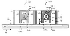
- FIG. 5Ais a cross sectional diagram illustrating the reactors 136 A, 136 B taken along line A-B of FIG. 4 , according to one embodiment.
- the injector 136 Aincludes a body 500 formed with a gas channel 516 , perforations (slits or holes) 520 , a reaction chamber 514 , constriction zones 518 A, 518 B, and exhaust portions 510 A, 510 B.
- the source precursoris injected into the reaction chamber 514 via the gas channel 516 and the perforations 520 .
- the region of the substrate 120 below the reaction chamber 514comes into contact with the source precursor and absorbs source precursor molecules on its surface.
- the excess source precursor(i.e., source precursor remaining after the source precursor is deposited on the substrate 120 ) passes through the constriction zones 518 A, 518 B, and are discharged via the exhaust portions 510 A, 510 B.
- the exhaust portions 510 A, 510 Bare connected to the exhaust pipes 422 A, 422 B.
- source precursor moleculespass the constriction zones 518 A, 518 B, physisorbed source precursor molecules are at least partially removed from the region of the substrate 120 below these zones 518 A, 518 B due to higher flow rate of the source precursor molecules.
- the injector 136 Amay also inject purge gas onto the substrate 120 to remove physisorbed source precursor molecules from the substrate 120 , leaving only chemisorbed source precursor molecules on the substrate 120 . In this way, an ALD process yielding a high quality atomic layer can be obtained.
- the radical reactor 136 Bhas a similar structure as the injector 136 A except that the radical reactor further includes a plasma generator.
- the plasma generatorincludes an inner electrode 576 and an outer electrode 572 surrounding a plasma chamber 578 (the outer electrode 572 may be part of a metallic body 550 ).
- the body 550is formed with, among others, a gas channel 564 , perforations (slits or holes) 568 , the plasma chamber 578 , an injector slit 580 , a reaction chamber 562 and exhaust portions 560 A, 560 B.
- a gas or a mixture of gasesis injected via the channel 564 and perforations 568 into the plasma chamber 578 .
- the distance H between the plasma chamber 578 and the substrate 120is configured so that a sufficient amount of radicals reach the substrate 120 in an active state. Radicals have a predetermined lifetime. Hence, as the radicals travel via the injector slit 580 and the reaction chamber 562 to the substrate 120 , some of the radicals revert back to an inactive gaseous state. With the increase in the travel distance, the amount of radicals reverting to the inactive gaseous state increases. Hence, it is advantageous to set the distance H to be less than a certain length. For example, the distance H is set to 10 to 100 mm.
- the lifespan of the radicalsis relatively short and most of the radicals revert back to an inactive state if the distance H is 80 mm or more.
- the distance His set to be less than 80 mm when using radicals of nitrogen containing gas mixtures.
- FIG. 5Bis a graph illustrating the concentration of nitrogen in a deposited layer in relation to a distance H of the substrate 120 from the plasma chamber 578 .
- the substrate 120was injected with Trimethylaluminium (TMA) and then injected with the radicals of a gas mixture including 50% of N 2 O and 50% of NH 3 , thereby depositing atomic layer AlON on the substrate 120 .
- TMATrimethylaluminium
- N*nitrogen radicals
- the content of nitrogen in the deposited layeris a function of the amount of active radicals that reach the surface of the substrate 120 in an active state. With increase in the distance H, the content of nitrogen in the deposited layer is decreased.
- the decrease in the nitrogen contentindicates that the nitrogen radicals N* are not effectively reaching the substrate 120 .
- the content of nitrogen in the deposited layerdrops significantly if the distance H increases to 80 mm or more. Therefore, it is advantageous to maintain the distance H to less than 80 mm when nitrogen radicals N* are used as reactant precursor.
- the temperature of the substrate 120was maintained at 80° C. and the temperature of the TMA gas canister was maintained at 5° C.
- the plasmawas generated in the plasma chamber 578 by applying DC pulse of 120 kHz at 200 watts.
- the resulting deposition rate of AlON filmwas 1.70 ⁇ /cycle.
- FIG. 6is a cross sectional diagram illustrating a radical reactor 600 , according to another embodiment.
- the radical reactor 600includes a body 610 and an inner electrode 614 extending across the radical reactor 600 .
- the inner electrodehas a semi-circular cross section where the flat surface faces the substrate 120 and the circular surface faces away from the substrate 120 .
- a gas or mixture of gasesis injected into the radical reactor 600 via a channel 618 and perforations 622 formed in the body 610 of the radical reactor.
- Part 624 of the body 610functions as an outer electrode.
- radicalscan be generated in a plasma region 628 .
- the radicalsflow into the exhaust portions 626 A, 626 B via constriction zones 642 A, 642 B.
- the principle and operation of depositing an atomic layer in the radical reactor 600are substantially the same as the radical reactor 136 B, and are omitted herein for the sake of brevity. Radical reactors of various other configurations may also be used.
- radicals generated from a mixture of N 2 O gas and NH 3 gasresulted in a higher deposition rate compared to using only N 2 O gas or NH 3 gas.
- particleswere formed at certain mixture ratio of gases.
- experimentswere performed to identify a range of mixture ratio that resulted in a higher deposition rate while avoiding the formation of particles in the radical reactor 136 B, as described below in detail with reference to Table 1.
- TMAwas first injected on the substrate and then injected with radicals of gas(es) to form a film of AlN, Al 2 O 3 or AlON.
- the temperature of the substratewas maintained at 80° C. and the temperature of TMA gas was maintained at 5° C.
- radicals used as reactant precursorNH 3 , N 2 O or a mixture thereof was used.
- a voltage signal of 120 kHz at 200 wattwas applied between the inner electrode 576 and the outer electrode 572 .
- the distance H (See FIG. 5 ) between the substrate and the plasma chamberwas 17 mm.
- the length of the radial reactorwas 260 mm.
- the diameter of the susceptor holding the substratewas 80 cm and the rotation speed of the susceptor was 5 rpm.
- the measured deposition rate of AlN, Al 2 O 3 or AlON layer and characteristic of these layersare tabulated in Table 1.
- NH 3 and N 2 Owere injected into the radical reactor at a ratio of x (for NH 3 gas, where x takes a value between 0 and 1) to (1 ⁇ x)(for N2O gas)
- the deposition ratewas greatest (1.96 ⁇ /cycle) when the ratio between N 2 O gas and NH 3 gas was 80:20. At this ratio, no particle was generated in the radical reactor. When the NH 3 was increased or decreased beyond this ratio, the deposition rate decreased. Moreover, as the ratio of NH 3 increased to 40%, particles were formed in the radical reactor. Specifically, particles were detected in the radical reactor when ratio of N 2 O and NH 3 ranged from 40:60 to 60:40. The particles were not detected when the ratio of NH 3 increased to 70% and above. Table 1 shows that it is advantageous to use the radicals of nitrogen containing gas mixture instead of using only N 2 O or NH 3 to improve the deposition rate.
- Tetraethylmethylaminozirconiummay be used as the source precursor and similar mixture of (1 ⁇ x)N 2 O and (x)NH 3 (where x takes a value above 0 and below 0.5) may be used to generate radicals as the reactant precursor to generate a layer of ZrO (1-x) N x on the substrate.
- TEMAZrTetraethylmethylaminozirconium
- Trimethylsilane(TMS, (CH 3 ) 3 SiH) or Tridimethylaminesilicone (3DMAS) may be used as the source precursor and a gas of (1 ⁇ x)NH 3 and (x)N 2 O (where x is above 0 and below 0.5) may be used to generate radicals acting as reactant precursor to obtain a layer of SiO x N (1-x) .
- the mixture of gas for generating radicalsis not limited to nitrogen containing gases.
- NH 3may be mixed with CH 4 to generate N* and C* radicals.
- Tetraethylmethylaluminumtitanium (TEMATi)is used as the source precursor and radicals generated from (1 ⁇ x)NH 3 and (x)CH 4 (where x is above 0 and below 50) are used as the reactant precursor to form a layer of TiC (1-x) N x on a substrate.
- TiCl 4is used as the source precursor and radicals generated from N 2 or NH 3 gas are used as the reactant precursor to generate an atomic layer of TiN film on a substrate.
- the distance H from the substrate to the plasma chambermay be set to be less than 80 mm so that most of the radicals may reach the substrate without reverting back to an inactive state.
- FIG. 7is a flowchart illustrating a process of performing atomic layer depositing using radicals of a nitrogen containing gas mixture, according to one embodiment.
- the source precursoris injected 710 onto a region of substrate by the injector 136 A.
- relative movementis caused 720 between the substrate 120 and the injector assembly 136 to place the region of substrate 120 below the radical reactor 720 .
- the radical reactor 136 Bis injected with a mixture of gas.
- the gas mixturemay include a first gas and a second gas.
- the first gasmay be NH 3 and the second gas may be N 2 O.
- the deposition rate of the ALD processcan be increased.
- the deposited layeris AlON.
Landscapes
- Chemical & Material Sciences (AREA)
- Engineering & Computer Science (AREA)
- Mechanical Engineering (AREA)
- Chemical Kinetics & Catalysis (AREA)
- General Chemical & Material Sciences (AREA)
- Materials Engineering (AREA)
- Metallurgy (AREA)
- Organic Chemistry (AREA)
- Inorganic Chemistry (AREA)
- Physics & Mathematics (AREA)
- Plasma & Fusion (AREA)
- Electromagnetism (AREA)
- Chemical Vapour Deposition (AREA)
Abstract
Description
- This application claims priority under 35 U.S.C. §119(e) to co-pending U.S. Provisional Patent Application No. 61/443,556, filed on Feb. 16, 2011, which is incorporated by reference herein in its entirety.
- 1. Field of Art
- The present invention relates to depositing one or more layers of materials on a substrate using atomic layer deposition (ALD).
- 2. Description of the Related Art
- An atomic layer deposition (ALD) is a thin film deposition technique for depositing one or more layers of material on a substrate. ALD uses two types of chemical, one is a source precursor and the other is a reactant precursor. Generally, ALD includes four stages: (i) injection of a source precursor, (ii) removal of a physical adsorption layer of the source precursor, (iii) injection of a reactant precursor, and (iv) removal of a physical adsorption layer of the reactant precursor. ALD can be a slow process that can take an extended amount of time or many repetitions before a layer of desired thickness can be obtained. Hence, to expedite the process, a vapor deposition reactor with a unit module (so-called a linear injector), as described in U.S. Patent Application Publication No. 2009/0165715 or other similar devices may be used to expedite ALD process. The unit module includes an injection unit and an exhaust unit for a source material (a source module), and an injection unit and an exhaust unit for a reactant (a reactant module).
- A conventional ALD vapor deposition chamber has one or more sets of reactors for depositing ALD layers on substrates. As the substrate passes below the reactors, the substrate is exposed to the source precursor, a purge gas and the reactant precursor. The source precursor molecules deposited on the substrate reacts with reactant precursor molecules or the source precursor molecules are replaced with the reactant precursor molecules to deposit a layer of material on the substrate. After exposing the substrate to the source precursor or the reactant precursor, the substrate may be exposed to the purge gas to remove excess source precursor molecules or reactant precursor molecules from the substrate.
- To reduce the number of reiteration needed to deposit a material of a desired thickness, it is advantageous to increase the deposition rate per each ALD cycle.
- Embodiments relate to depositing a layer of material on a substrate by generating radicals of a gas mixture containing a first gas and a second gas and then injecting the radicals onto a substrate. The first gas includes a nitrogen compound. The substrate is previously injected with a source precursor. The radicals function as a reactant precursor reacting with or replacing source precursor molecules on the substrate and depositing a layer of material on the substrate.
- In one embodiment, the second gas includes another nitrogen compound. The first gas may include NH3and the second gas may include N2O.
- In one embodiment, the deposited material comprises aluminum oxynitride (AlON).
- In one embodiment, the ratio of N2O and NH3is 70:30 to 90:10. More preferably, the ratio of N2O and NH3is 80:20.
- In one embodiment, the mixture of gases is injected into a plasma chamber in a radical reactor. A voltage is applied between a first electrode in the plasma chamber and a second electrode surrounding the plasma chamber to generate plasma in the plasma chamber. The plasma generates radicals of the mixture of gases.
- In one embodiment, the distance from the plasma chamber to the substrate is less than 80 mm.
- In one embodiment, the source precursor is selected from a group consisting of Tetraethylmethylaminozirconium (TEMAZr), Trimethylsilane (TMS), Tridimethylaminesilicone (3DMAS) and Tetraethylmethylaluminumtitanium (TEMATi).
- In one embodiment, the first gas comprises NH3and the second gas comprises CH4.
- Embodiments also relate to a radical reactor comprising a body and an electrode to generate radicals functioning as a reactant precursor in an atomic layer deposition (ALD) process. The body is formed with a channel for supplying gas, a plasma chamber connected to the channel to receive the supplied gas and generate radicals of the supplied gas, a reaction chamber connected to the plasma chamber to receive the generated radicals and located above a substrate to expose the substrate to the radicals, and one or more exhaust portions to discharge excess gas and/or radicals. An electrode extends within the body. A voltage is applied across the electrode and the body to generate plasma in the plasma chamber.
FIG. 1 is a cross sectional diagram of a linear deposition device, according to one embodiment.FIG. 2 is a perspective view of a linear deposition device, according to one embodiment.FIG. 3 is a perspective view of a rotating deposition device, according to one embodiment.FIG. 4 is a perspective view of reactors in a deposition device, according to one embodiment.FIG. 5A is a cross sectional diagram illustrating the reactors taken along line A-B ofFIG. 4 , according to one embodiment.FIG. 5B is a graph illustrating concentration of nitrogen in a deposited layer in relation to a distance of a substrate from a plasma chamber.FIG. 6 is a cross sectional diagram illustrating a radical reactor, according to another embodiment.FIG. 7 is a flowchart illustrating a process of performing atomic layer depositing using radicals of nitrogen containing gas mixture, according to one embodiment.- Embodiments are described herein with reference to the accompanying drawings. Principles disclosed herein may, however, be embodied in many different forms and should not be construed as being limited to the embodiments set forth herein. In the description, details of well-known features and techniques may be omitted to avoid unnecessarily obscuring the features of the embodiments.
- In the drawings, like reference numerals in the drawings denote like elements. The shape, size and regions, and the like, of the drawing may be exaggerated for clarity.
- Embodiments relate to performing atomic layer deposition (ALD) using a gas mixture to generate radicals that function as a reactant precursor for depositing a layer of material on a substrate. The gas mixture includes a nitrogen containing compound such as NH3or N2O. The substrate is previously injected with a source precursor material. Hence, when the substrate is injected with the reactant precursor, a layer of material is deposited on the substrate. By using a mixture of gases instead of a single gas to generate radicals, the deposition rate of the material can be increased.
FIG. 1 is a cross sectional diagram of alinear deposition device 100, according to one embodiment.FIG. 2 is a perspective view of the linear deposition device100 (without chamber walls to facilitate explanation), according to one embodiment. Thelinear deposition device 100 may include, among other components, asupport pillar 118, theprocess chamber 110 and one ormore reactors 136. Thereactors 136 may include one or more of injectors and radical reactors. Each of the injectors injects source precursors, reactant precursors, purge gases or a combination of these materials onto thesubstrate 120. As described below in detail with reference toFIG. 5 , source precursors and/or reactant precursors may be radicals of a gas mixture.- The process chamber enclosed by the walls may be maintained in a vacuum state to prevent contaminants from affecting the deposition process. The
process chamber 110 contains asusceptor 128 which receives asubstrate 120. Thesusceptor 128 is placed on asupport plate 124 for a sliding movement. Thesupport plate 124 may include a temperature controller (e.g., a heater or a cooler) to control the temperature of thesubstrate 120. Thelinear deposition device 100 may also include lift pins (not shown) that facilitate loading of thesubstrate 120 onto thesusceptor 128 or dismounting of thesubstrate 120 from thesusceptor 128. - In one embodiment, the
susceptor 128 is secured tobrackets 210 that move across anextended bar 138 with screws formed thereon. Thebrackets 210 have corresponding screws formed in their holes receiving theextended bar 138. Theextended bar 138 is secured to a spindle of amotor 114, and hence, theextended bar 138 rotates as the spindle of themotor 114 rotates. The rotation of theextended bar 138 causes the brackets210 (and therefore the susceptor128) to make a linear movement on thesupport plate 124. By controlling the speed and rotation direction of themotor 114, the speed and the direction of the linear movement of thesusceptor 128 can be controlled. The use of amotor 114 and theextended bar 138 is merely an example of a mechanism for moving thesusceptor 128. Various other ways of moving the susceptor128 (e.g., use of gears and pinion at the bottom, top or side of the susceptor128). Moreover, instead of moving thesusceptor 128, thesusceptor 128 may remain stationary and thereactors 136 may be moved. FIG. 3 is a perspective view of arotating deposition device 300, according to one embodiment. Instead of using thelinear deposition device 100 ofFIG. 1 , therotating deposition device 300 may be used to perform the deposition process according to another embodiment. Therotating deposition device 300 may include, among other components,reactors susceptor 318, and acontainer 324 enclosing these components. A set of reactors (e.g.,320A and320B) of therotating deposition device 300 correspond to thereactors 136 of thelinear deposition device 100, as described above with reference toFIG. 1 . Thesusceptor 318 secures thesubstrates 314 in place. Thereactors substrates 314 and thesusceptor 318. Either thesusceptor 318 or the reactors320,334,364,368 rotate to subject thesubstrates 314 to different processes.- One or more of the
reactors substrate 314 directly by thereactors reactors reactors substrate 314, the redundant materials may be exhausted throughoutlets rotating deposition device 300 may also be maintained in a vacuum state. - Although following example embodiments are described primarily with reference to the
reactors 136 in thelinear deposition device 100, the same principle and operation can be applied to therotating deposition device 300 or other types of deposition device. FIG. 4 is a perspective view ofreactors reactors 136”) in thedeposition device 100 ofFIG. 1 , according to one embodiment. InFIG. 4 , thereactors reactors substrate 120 moves from the left to the right (as shown by arrow450), thesubstrate 120 is sequentially injected with materials by thereactors deposition layer 410 on thesubstrate 120. Instead of moving thesubstrate 120, thereactors - In one or more embodiments, the
reactor 136A is a gas injector that injects source precursor materials onto thesubstrate 120. Thereactor 136A is connected to a pipe (not shown) to receive the source precursor from a source (e.g., a canister). The source precursor is injected onto thesubstrate 120, forming one or more layers of source precursor molecules on thesubstrate 120. Excess source precursor molecules are exhausted viaexhaust pipes - The
reactor 136B may be a radical reactor that generates radicals of gas or a gas mixture received from one or more sources (e.g., canisters). The radicals of gas or gas mixture may function as reactant precursor that forms an atomic layer of materials on thesubstrate 120 in conjunction with the source precursor. The gas or gas mixtures are injected into thereactor 136B via a pipe (not shown), and are converted into radicals within thereactor 136B by applying voltage across electrodes. The radicals are injected onto thesubstrate 120, and remaining radicals and/or gas reverted to inactive state are discharged from thereactor 136B viaexhaust pipes FIG. 5A is a cross sectional diagram illustrating thereactors FIG. 4 , according to one embodiment. Theinjector 136A includes abody 500 formed with agas channel 516, perforations (slits or holes)520, areaction chamber 514,constriction zones exhaust portions reaction chamber 514 via thegas channel 516 and theperforations 520. The region of thesubstrate 120 below thereaction chamber 514 comes into contact with the source precursor and absorbs source precursor molecules on its surface. The excess source precursor (i.e., source precursor remaining after the source precursor is deposited on the substrate120) passes through theconstriction zones exhaust portions exhaust portions exhaust pipes - While the source precursor molecules pass the
constriction zones substrate 120 below thesezones - In one or more embodiment, the
injector 136A may also inject purge gas onto thesubstrate 120 to remove physisorbed source precursor molecules from thesubstrate 120, leaving only chemisorbed source precursor molecules on thesubstrate 120. In this way, an ALD process yielding a high quality atomic layer can be obtained. - The
radical reactor 136B has a similar structure as theinjector 136A except that the radical reactor further includes a plasma generator. The plasma generator includes aninner electrode 576 and anouter electrode 572 surrounding a plasma chamber578 (theouter electrode 572 may be part of a metallic body550). Thebody 550 is formed with, among others, agas channel 564, perforations (slits or holes)568, theplasma chamber 578, aninjector slit 580, areaction chamber 562 andexhaust portions channel 564 andperforations 568 into theplasma chamber 578. By applying a voltage difference between theinner electrode 576 and theouter electrode 572, plasma is generated in theplasma chamber 578. As a result of the plasma, radicals of the gas or the mixture of gases are generated within theplasma chamber 578. The generated radicals are injected into thereaction chamber 562 via theinjector slit 580. The region of thesubstrate 120 below thereaction chamber 562 comes into contact with the radicals, forming the depositedlayer 410 on thesubstrate 120. - The distance H between the
plasma chamber 578 and thesubstrate 120 is configured so that a sufficient amount of radicals reach thesubstrate 120 in an active state. Radicals have a predetermined lifetime. Hence, as the radicals travel via the injector slit580 and thereaction chamber 562 to thesubstrate 120, some of the radicals revert back to an inactive gaseous state. With the increase in the travel distance, the amount of radicals reverting to the inactive gaseous state increases. Hence, it is advantageous to set the distance H to be less than a certain length. For example, the distance H is set to 10 to 100 mm. - When using radicals of nitrogen containing gas mixtures (e.g., N2O and NH3mixture), the lifespan of the radicals is relatively short and most of the radicals revert back to an inactive state if the distance H is 80 mm or more. Hence, the distance H is set to be less than 80 mm when using radicals of nitrogen containing gas mixtures.
FIG. 5B is a graph illustrating the concentration of nitrogen in a deposited layer in relation to a distance H of thesubstrate 120 from theplasma chamber 578. In the experiment ofFIG. 5B , thesubstrate 120 was injected with Trimethylaluminium (TMA) and then injected with the radicals of a gas mixture including 50% of N2O and 50% of NH3, thereby depositing atomic layer AlON on thesubstrate 120. As more nitrogen radicals (N*) remain active, more nitrogen atoms become incorporated into the deposited AlON layer. Hence, the content of nitrogen in the deposited layer is a function of the amount of active radicals that reach the surface of thesubstrate 120 in an active state. With increase in the distance H, the content of nitrogen in the deposited layer is decreased. The decrease in the nitrogen content indicates that the nitrogen radicals N* are not effectively reaching thesubstrate 120. Referring toFIG. 5B , the content of nitrogen in the deposited layer drops significantly if the distance H increases to 80 mm or more. Therefore, it is advantageous to maintain the distance H to less than 80 mm when nitrogen radicals N* are used as reactant precursor.- For the purpose of experiment illustrated in
FIG. 5B , the temperature of thesubstrate 120 was maintained at 80° C. and the temperature of the TMA gas canister was maintained at 5° C. The plasma was generated in theplasma chamber 578 by applying DC pulse of 120 kHz at 200 watts. The resulting deposition rate of AlON film was 1.70 Å/cycle. FIG. 6 is a cross sectional diagram illustrating aradical reactor 600, according to another embodiment. Theradical reactor 600 includes abody 610 and aninner electrode 614 extending across theradical reactor 600. The inner electrode has a semi-circular cross section where the flat surface faces thesubstrate 120 and the circular surface faces away from thesubstrate 120.- A gas or mixture of gases is injected into the
radical reactor 600 via achannel 618 andperforations 622 formed in thebody 610 of the radical reactor. Part624 of thebody 610 functions as an outer electrode. By applying the voltage between theinner electrode 614 and theouter electrode 624, radicals can be generated in aplasma region 628. The radicals flow into theexhaust portions constriction zones radical reactor 600 are substantially the same as theradical reactor 136B, and are omitted herein for the sake of brevity. Radical reactors of various other configurations may also be used. - When generating radicals of nitrogen, it is advantageous to use a mixture of gases instead of using a single gas. For example, based on experiments, radicals generated from a mixture of N2O gas and NH3gas resulted in a higher deposition rate compared to using only N2O gas or NH3gas. However, particles were formed at certain mixture ratio of gases. Hence, experiments were performed to identify a range of mixture ratio that resulted in a higher deposition rate while avoiding the formation of particles in the
radical reactor 136B, as described below in detail with reference to Table 1. - In the following experiments, TMA was first injected on the substrate and then injected with radicals of gas(es) to form a film of AlN, Al2O3or AlON. The temperature of the substrate was maintained at 80° C. and the temperature of TMA gas was maintained at 5° C. To generate radicals used as reactant precursor, NH3, N2O or a mixture thereof was used. To generate the plasma, a voltage signal of 120 kHz at 200 watt was applied between the
inner electrode 576 and theouter electrode 572. The distance H (SeeFIG. 5 ) between the substrate and the plasma chamber was 17 mm. The length of the radial reactor was 260 mm. The diameter of the susceptor holding the substrate was 80 cm and the rotation speed of the susceptor was 5 rpm. - The measured deposition rate of AlN, Al2O3or AlON layer and characteristic of these layers are tabulated in Table 1. When NH3and N2O were injected into the radical reactor at a ratio of x (for NH3gas, where x takes a value between 0 and 1) to (1−x)(for N2O gas), the resulting layer was Al2O3(when x=1), AlN (when x=0) or (x)Al2O3+(1−x)AlN.
TABLE 1 N2O:NH3 0:100 10:90 20:80 30:70 40:60 50:50 60:40 70:30 80:20 90:10 100:0 Refractive 1.559 1.632 1.629 1.626 1.629 1.632 1.626 1.615 1.607 1.621 1.637 Index (n) Dep. Rate 0.44 1.48 1.57 1.68 1.35 1.70 1.81 1.88 1.96 1.91 1.31 (Å/cycle) Particle No No No No Yes Yes Yes No No No No generated? - As seen in Table 1, the deposition rate was greatest (1.96 Å/cycle) when the ratio between N2O gas and NH3gas was 80:20. At this ratio, no particle was generated in the radical reactor. When the NH3was increased or decreased beyond this ratio, the deposition rate decreased. Moreover, as the ratio of NH3increased to 40%, particles were formed in the radical reactor. Specifically, particles were detected in the radical reactor when ratio of N2O and NH3ranged from 40:60 to 60:40. The particles were not detected when the ratio of NH3increased to 70% and above. Table 1 shows that it is advantageous to use the radicals of nitrogen containing gas mixture instead of using only N2O or NH3to improve the deposition rate.
- In another embodiment, Tetraethylmethylaminozirconium (TEMAZr) may be used as the source precursor and similar mixture of (1−x)N2O and (x)NH3(where x takes a value above 0 and below 0.5) may be used to generate radicals as the reactant precursor to generate a layer of ZrO(1-x)Nxon the substrate.
- In still another embodiment, Trimethylsilane (TMS, (CH3)3SiH) or Tridimethylaminesilicone (3DMAS) may be used as the source precursor and a gas of (1−x)NH3and (x)N2O (where x is above 0 and below 0.5) may be used to generate radicals acting as reactant precursor to obtain a layer of SiOxN(1-x).
- The mixture of gas for generating radicals is not limited to nitrogen containing gases. For example, NH3may be mixed with CH4to generate N* and C* radicals. In one embodiment, Tetraethylmethylaluminumtitanium (TEMATi) is used as the source precursor and radicals generated from (1−x)NH3and (x)CH4(where x is above 0 and below 50) are used as the reactant precursor to form a layer of TiC(1-x)Nxon a substrate.
- In still another embodiment, TiCl4is used as the source precursor and radicals generated from N2or NH3gas are used as the reactant precursor to generate an atomic layer of TiN film on a substrate.
- In the above embodiments, the distance H from the substrate to the plasma chamber may be set to be less than 80 mm so that most of the radicals may reach the substrate without reverting back to an inactive state.
FIG. 7 is a flowchart illustrating a process of performing atomic layer depositing using radicals of a nitrogen containing gas mixture, according to one embodiment. First, the source precursor is injected710 onto a region of substrate by theinjector 136A. Then, relative movement is caused720 between thesubstrate 120 and theinjector assembly 136 to place the region ofsubstrate 120 below the radical reactor720.- The
radical reactor 136B is injected with a mixture of gas. The gas mixture may include a first gas and a second gas. The first gas may be NH3and the second gas may be N2O. By using a mixture of two different gases, the deposition rate of the ALD process can be increased. In this example, the deposited layer is AlON. - Although the present invention has been described above with respect to several embodiments, various modifications can be made within the scope of the present invention. Accordingly, the disclosure of the present invention is intended to be illustrative, but not limiting, of the scope of the invention, which is set forth in the following claims.
Claims (20)
1. A method of depositing a layer of material on a substrate, comprising:
injecting a source precursor onto a substrate;
injecting a mixture of a first gas and a second gas into a radical reactor, wherein the first gas comprises a nitrogen compound;
generating radicals of the mixture of the first gas and the second gas; and
injecting the generated radicals onto the substrate, the generated radicals reacting with source precursor molecules or replacing the source precursor molecules to deposit a layer of material on the substrate.
2. The method ofclaim 1 , wherein the second gas comprises another nitrogen compound.
3. The method ofclaim 1 , wherein the first gas comprise NH3and the second gas comprises N2O.
4. The method ofclaim 3 , wherein the deposited material comprises aluminum oxynitride (AlON).
5. The method ofclaim 3 , wherein the ratio of N2O and NH3is 70:30 to 90:10.
6. The method ofclaim 5 , wherein the ratio of N2O and NH3is 80:20.
7. The method ofclaim 1 , wherein generating the radicals comprises:
injecting the mixture into a plasma chamber in the radical reactor; and
applying a voltage across a first electrode in the plasma chamber and a second electrode surrounding the plasma chamber.
8. The method ofclaim 1 , wherein a distance from the plasma chamber to the substrate is less than 80 mm.
9. The method ofclaim 1 , wherein the source precursor is selected from a group consisting of Tetraethylmethylaminozirconium (TEMAZr), Trimethylsilane (TMS), Tridimethylaminesilicone (3DMAS) and Tetraethylmethylaluminumtitanium (TEMATi).
10. The method ofclaim 1 , wherein the first gas comprises NH3and the second gas comprises CH4.
11. A radical reactor for generating radicals of gas, comprising:
a body formed with a channel for supplying gas, a plasma chamber connected to the channel to receive the supplied gas and generate radicals of the supplied gas, a reaction chamber connected to the plasma chamber to receive the generated radicals and located above a substrate to expose the substrate to the radicals, and one or more exhaust portions to discharge excess gas or radicals; and
an electrode extending in the body, voltage applied across the electrode and the body to generate plasma in the plasma chamber.
12. The radical reactor ofclaim 11 , wherein the gas comprises a mixture of a first gas and a second gas, wherein the first gas comprises a nitrogen compound.
13. The radical reactor ofclaim 12 , wherein the first gas comprise NH3and the second gas comprises N2O.
14. The radical reactor ofclaim 13 , wherein exposure of the substrate to the radicals deposit aluminum oxynitride (AlON) on the substrate.
15. The radical reactor ofclaim 13 , wherein the ratio of N2O and NH3is 70:30 to 90:10.
16. The radical reactor ofclaim 11 , wherein a distance from the substrate to the plasma chamber is less than 80 mm.
17. The radical reactor ofclaim 11 , wherein the body is further formed with a perforation connecting the plasma chamber and the reactor chamber.
18. The radical reactor ofclaim 11 , wherein at least part of the radical reactor is placed in a vacuum state.
19. The radical reactor ofclaim 11 , wherein the substrate contains a layer of material selected from a group consisting of Tetraethylmethylaminozirconium (TEMAZr), Trimethylsilane (TMS), Tridimethylaminesilicone (3DMAS) and Tetraethylmethylaluminumtitanium (TEMATi).
20. The radical reactor ofclaim 12 , wherein the first gas comprises NH3and the second gas comprises CH4.
Priority Applications (5)
| Application Number | Priority Date | Filing Date | Title |
|---|---|---|---|
| US13/369,717US8877300B2 (en) | 2011-02-16 | 2012-02-09 | Atomic layer deposition using radicals of gas mixture |
| PCT/US2012/025095WO2012112584A2 (en) | 2011-02-16 | 2012-02-14 | Atomic layer deposition using radicals of gas mixture |
| KR1020137024157AKR101608368B1 (en) | 2011-02-16 | 2012-02-14 | Atomic layer deposition using radicals of gas mixture |
| TW101105141ATWI512134B (en) | 2011-02-16 | 2012-02-16 | Atomic layer deposition using radicals of gas mixture |
| US14/503,735US20150020737A1 (en) | 2011-02-16 | 2014-10-01 | Atomic Layer Deposition Using Radicals Of Gas Mixture |
Applications Claiming Priority (2)
| Application Number | Priority Date | Filing Date | Title |
|---|---|---|---|
| US201161443556P | 2011-02-16 | 2011-02-16 | |
| US13/369,717US8877300B2 (en) | 2011-02-16 | 2012-02-09 | Atomic layer deposition using radicals of gas mixture |
Related Child Applications (1)
| Application Number | Title | Priority Date | Filing Date |
|---|---|---|---|
| US14/503,735DivisionUS20150020737A1 (en) | 2011-02-16 | 2014-10-01 | Atomic Layer Deposition Using Radicals Of Gas Mixture |
Publications (2)
| Publication Number | Publication Date |
|---|---|
| US20120207948A1true US20120207948A1 (en) | 2012-08-16 |
| US8877300B2 US8877300B2 (en) | 2014-11-04 |
Family
ID=46637101
Family Applications (2)
| Application Number | Title | Priority Date | Filing Date |
|---|---|---|---|
| US13/369,717Expired - Fee RelatedUS8877300B2 (en) | 2011-02-16 | 2012-02-09 | Atomic layer deposition using radicals of gas mixture |
| US14/503,735AbandonedUS20150020737A1 (en) | 2011-02-16 | 2014-10-01 | Atomic Layer Deposition Using Radicals Of Gas Mixture |
Family Applications After (1)
| Application Number | Title | Priority Date | Filing Date |
|---|---|---|---|
| US14/503,735AbandonedUS20150020737A1 (en) | 2011-02-16 | 2014-10-01 | Atomic Layer Deposition Using Radicals Of Gas Mixture |
Country Status (4)
| Country | Link |
|---|---|
| US (2) | US8877300B2 (en) |
| KR (1) | KR101608368B1 (en) |
| TW (1) | TWI512134B (en) |
| WO (1) | WO2012112584A2 (en) |
Cited By (22)
| Publication number | Priority date | Publication date | Assignee | Title |
|---|---|---|---|---|
| US20100037824A1 (en)* | 2008-08-13 | 2010-02-18 | Synos Technology, Inc. | Plasma Reactor Having Injector |
| US20100064971A1 (en)* | 2008-09-17 | 2010-03-18 | Synos Technology, Inc. | Electrode for Generating Plasma and Plasma Generator |
| US20100068413A1 (en)* | 2008-09-17 | 2010-03-18 | Synos Technology, Inc. | Vapor deposition reactor using plasma and method for forming thin film using the same |
| US20100181566A1 (en)* | 2009-01-21 | 2010-07-22 | Synos Technology, Inc. | Electrode Structure, Device Comprising the Same and Method for Forming Electrode Structure |
| US20100310771A1 (en)* | 2009-06-08 | 2010-12-09 | Synos Technology, Inc. | Vapor deposition reactor and method for forming thin film |
| US8574728B2 (en) | 2011-03-15 | 2013-11-05 | Kennametal Inc. | Aluminum oxynitride coated article and method of making the same |
| KR20140033659A (en)* | 2012-09-10 | 2014-03-19 | 주성엔지니어링(주) | Apparatus and method of processing substrate |
| US8771791B2 (en) | 2010-10-18 | 2014-07-08 | Veeco Ald Inc. | Deposition of layer using depositing apparatus with reciprocating susceptor |
| US20140205769A1 (en)* | 2013-01-22 | 2014-07-24 | Veeco Ald Inc. | Cascaded plasma reactor |
| WO2014176077A1 (en)* | 2013-04-25 | 2014-10-30 | Veeco Ald Inc. | Thin film formation for device sensitive to environment |
| US8895108B2 (en) | 2009-02-23 | 2014-11-25 | Veeco Ald Inc. | Method for forming thin film using radicals generated by plasma |
| US9017809B2 (en) | 2013-01-25 | 2015-04-28 | Kennametal Inc. | Coatings for cutting tools |
| US20150225848A1 (en)* | 2012-08-23 | 2015-08-13 | Jusung Engineering Co. Ltd. | Substrate treatment apparatus and substrate treatment method |
| US9138864B2 (en) | 2013-01-25 | 2015-09-22 | Kennametal Inc. | Green colored refractory coatings for cutting tools |
| US9163310B2 (en) | 2011-02-18 | 2015-10-20 | Veeco Ald Inc. | Enhanced deposition of layer on substrate using radicals |
| US9427808B2 (en) | 2013-08-30 | 2016-08-30 | Kennametal Inc. | Refractory coatings for cutting tools |
| US9613800B2 (en) | 2014-02-20 | 2017-04-04 | Samsung Electronics Co., Ltd. | Methods of manufacturing semiconductor devices including an oxide layer |
| US9799509B2 (en)* | 2014-11-26 | 2017-10-24 | Asm Ip Holding B.V. | Cyclic aluminum oxynitride deposition |
| CN107400878A (en)* | 2017-07-26 | 2017-11-28 | 北京芯微诺达科技有限公司 | The gas handling system and its method of a kind of atomic layer deposition apparatus |
| US9837281B2 (en) | 2014-11-26 | 2017-12-05 | Asm Ip Holding B.V. | Cyclic doped aluminum nitride deposition |
| US20180277400A1 (en)* | 2017-03-23 | 2018-09-27 | Toshiba Memory Corporation | Semiconductor manufacturing apparatus |
| US10815569B2 (en) | 2015-08-28 | 2020-10-27 | Samsung Electronics Co., Ltd. | Shower head of combinatorial spatial atomic layer deposition apparatus |
Families Citing this family (275)
| Publication number | Priority date | Publication date | Assignee | Title |
|---|---|---|---|---|
| US20130023129A1 (en) | 2011-07-20 | 2013-01-24 | Asm America, Inc. | Pressure transmitter for a semiconductor processing environment |
| US10714315B2 (en) | 2012-10-12 | 2020-07-14 | Asm Ip Holdings B.V. | Semiconductor reaction chamber showerhead |
| US20160376700A1 (en) | 2013-02-01 | 2016-12-29 | Asm Ip Holding B.V. | System for treatment of deposition reactor |
| US11015245B2 (en) | 2014-03-19 | 2021-05-25 | Asm Ip Holding B.V. | Gas-phase reactor and system having exhaust plenum and components thereof |
| US10941490B2 (en) | 2014-10-07 | 2021-03-09 | Asm Ip Holding B.V. | Multiple temperature range susceptor, assembly, reactor and system including the susceptor, and methods of using the same |
| US10276355B2 (en) | 2015-03-12 | 2019-04-30 | Asm Ip Holding B.V. | Multi-zone reactor, system including the reactor, and method of using the same |
| TWI723997B (en)* | 2015-06-19 | 2021-04-11 | 美商應用材料股份有限公司 | Injector for batch processing and methods of use |
| US10458018B2 (en) | 2015-06-26 | 2019-10-29 | Asm Ip Holding B.V. | Structures including metal carbide material, devices including the structures, and methods of forming same |
| US10211308B2 (en) | 2015-10-21 | 2019-02-19 | Asm Ip Holding B.V. | NbMC layers |
| US11139308B2 (en) | 2015-12-29 | 2021-10-05 | Asm Ip Holding B.V. | Atomic layer deposition of III-V compounds to form V-NAND devices |
| US10529554B2 (en) | 2016-02-19 | 2020-01-07 | Asm Ip Holding B.V. | Method for forming silicon nitride film selectively on sidewalls or flat surfaces of trenches |
| US10571430B2 (en) | 2016-03-14 | 2020-02-25 | Veeco Instruments Inc. | Gas concentration sensors and systems |
| US10343920B2 (en) | 2016-03-18 | 2019-07-09 | Asm Ip Holding B.V. | Aligned carbon nanotubes |
| US10367080B2 (en) | 2016-05-02 | 2019-07-30 | Asm Ip Holding B.V. | Method of forming a germanium oxynitride film |
| US11453943B2 (en) | 2016-05-25 | 2022-09-27 | Asm Ip Holding B.V. | Method for forming carbon-containing silicon/metal oxide or nitride film by ALD using silicon precursor and hydrocarbon precursor |
| US9859151B1 (en) | 2016-07-08 | 2018-01-02 | Asm Ip Holding B.V. | Selective film deposition method to form air gaps |
| US10612137B2 (en) | 2016-07-08 | 2020-04-07 | Asm Ip Holdings B.V. | Organic reactants for atomic layer deposition |
| US9812320B1 (en) | 2016-07-28 | 2017-11-07 | Asm Ip Holding B.V. | Method and apparatus for filling a gap |
| KR102532607B1 (en) | 2016-07-28 | 2023-05-15 | 에이에스엠 아이피 홀딩 비.브이. | Substrate processing apparatus and method of operating the same |
| US9887082B1 (en) | 2016-07-28 | 2018-02-06 | Asm Ip Holding B.V. | Method and apparatus for filling a gap |
| US10513986B2 (en)* | 2016-10-05 | 2019-12-24 | Rolls-Royce North American Technologies, Inc. | Counter-rotating electric generator in turbine engine |
| US11532757B2 (en) | 2016-10-27 | 2022-12-20 | Asm Ip Holding B.V. | Deposition of charge trapping layers |
| US10714350B2 (en) | 2016-11-01 | 2020-07-14 | ASM IP Holdings, B.V. | Methods for forming a transition metal niobium nitride film on a substrate by atomic layer deposition and related semiconductor device structures |
| KR102546317B1 (en) | 2016-11-15 | 2023-06-21 | 에이에스엠 아이피 홀딩 비.브이. | Gas supply unit and substrate processing apparatus including the same |
| KR102762543B1 (en) | 2016-12-14 | 2025-02-05 | 에이에스엠 아이피 홀딩 비.브이. | Substrate processing apparatus |
| US11447861B2 (en) | 2016-12-15 | 2022-09-20 | Asm Ip Holding B.V. | Sequential infiltration synthesis apparatus and a method of forming a patterned structure |
| US11581186B2 (en) | 2016-12-15 | 2023-02-14 | Asm Ip Holding B.V. | Sequential infiltration synthesis apparatus |
| KR102700194B1 (en) | 2016-12-19 | 2024-08-28 | 에이에스엠 아이피 홀딩 비.브이. | Substrate processing apparatus |
| US10269558B2 (en) | 2016-12-22 | 2019-04-23 | Asm Ip Holding B.V. | Method of forming a structure on a substrate |
| US11390950B2 (en) | 2017-01-10 | 2022-07-19 | Asm Ip Holding B.V. | Reactor system and method to reduce residue buildup during a film deposition process |
| US10468261B2 (en) | 2017-02-15 | 2019-11-05 | Asm Ip Holding B.V. | Methods for forming a metallic film on a substrate by cyclical deposition and related semiconductor device structures |
| US10529563B2 (en) | 2017-03-29 | 2020-01-07 | Asm Ip Holdings B.V. | Method for forming doped metal oxide films on a substrate by cyclical deposition and related semiconductor device structures |
| US10770286B2 (en) | 2017-05-08 | 2020-09-08 | Asm Ip Holdings B.V. | Methods for selectively forming a silicon nitride film on a substrate and related semiconductor device structures |
| US12040200B2 (en) | 2017-06-20 | 2024-07-16 | Asm Ip Holding B.V. | Semiconductor processing apparatus and methods for calibrating a semiconductor processing apparatus |
| US11306395B2 (en) | 2017-06-28 | 2022-04-19 | Asm Ip Holding B.V. | Methods for depositing a transition metal nitride film on a substrate by atomic layer deposition and related deposition apparatus |
| KR20190009245A (en) | 2017-07-18 | 2019-01-28 | 에이에스엠 아이피 홀딩 비.브이. | Methods for forming a semiconductor device structure and related semiconductor device structures |
| US11018002B2 (en) | 2017-07-19 | 2021-05-25 | Asm Ip Holding B.V. | Method for selectively depositing a Group IV semiconductor and related semiconductor device structures |
| US11374112B2 (en) | 2017-07-19 | 2022-06-28 | Asm Ip Holding B.V. | Method for depositing a group IV semiconductor and related semiconductor device structures |
| US10541333B2 (en) | 2017-07-19 | 2020-01-21 | Asm Ip Holding B.V. | Method for depositing a group IV semiconductor and related semiconductor device structures |
| US10590535B2 (en) | 2017-07-26 | 2020-03-17 | Asm Ip Holdings B.V. | Chemical treatment, deposition and/or infiltration apparatus and method for using the same |
| TWI815813B (en) | 2017-08-04 | 2023-09-21 | 荷蘭商Asm智慧財產控股公司 | Showerhead assembly for distributing a gas within a reaction chamber |
| US10770336B2 (en) | 2017-08-08 | 2020-09-08 | Asm Ip Holding B.V. | Substrate lift mechanism and reactor including same |
| US10692741B2 (en) | 2017-08-08 | 2020-06-23 | Asm Ip Holdings B.V. | Radiation shield |
| US11769682B2 (en) | 2017-08-09 | 2023-09-26 | Asm Ip Holding B.V. | Storage apparatus for storing cassettes for substrates and processing apparatus equipped therewith |
| US11139191B2 (en) | 2017-08-09 | 2021-10-05 | Asm Ip Holding B.V. | Storage apparatus for storing cassettes for substrates and processing apparatus equipped therewith |
| US11830730B2 (en) | 2017-08-29 | 2023-11-28 | Asm Ip Holding B.V. | Layer forming method and apparatus |
| US11295980B2 (en) | 2017-08-30 | 2022-04-05 | Asm Ip Holding B.V. | Methods for depositing a molybdenum metal film over a dielectric surface of a substrate by a cyclical deposition process and related semiconductor device structures |
| KR102491945B1 (en) | 2017-08-30 | 2023-01-26 | 에이에스엠 아이피 홀딩 비.브이. | Substrate processing apparatus |
| US11056344B2 (en) | 2017-08-30 | 2021-07-06 | Asm Ip Holding B.V. | Layer forming method |
| US10658205B2 (en) | 2017-09-28 | 2020-05-19 | Asm Ip Holdings B.V. | Chemical dispensing apparatus and methods for dispensing a chemical to a reaction chamber |
| US10403504B2 (en) | 2017-10-05 | 2019-09-03 | Asm Ip Holding B.V. | Method for selectively depositing a metallic film on a substrate |
| US10923344B2 (en) | 2017-10-30 | 2021-02-16 | Asm Ip Holding B.V. | Methods for forming a semiconductor structure and related semiconductor structures |
| US11022879B2 (en) | 2017-11-24 | 2021-06-01 | Asm Ip Holding B.V. | Method of forming an enhanced unexposed photoresist layer |
| WO2019103613A1 (en) | 2017-11-27 | 2019-05-31 | Asm Ip Holding B.V. | A storage device for storing wafer cassettes for use with a batch furnace |
| CN111344522B (en) | 2017-11-27 | 2022-04-12 | 阿斯莫Ip控股公司 | Including clean mini-environment device |
| US10872771B2 (en) | 2018-01-16 | 2020-12-22 | Asm Ip Holding B. V. | Method for depositing a material film on a substrate within a reaction chamber by a cyclical deposition process and related device structures |
| TWI799494B (en) | 2018-01-19 | 2023-04-21 | 荷蘭商Asm 智慧財產控股公司 | Deposition method |
| KR102695659B1 (en) | 2018-01-19 | 2024-08-14 | 에이에스엠 아이피 홀딩 비.브이. | Method for depositing a gap filling layer by plasma assisted deposition |
| US11081345B2 (en) | 2018-02-06 | 2021-08-03 | Asm Ip Holding B.V. | Method of post-deposition treatment for silicon oxide film |
| US10896820B2 (en) | 2018-02-14 | 2021-01-19 | Asm Ip Holding B.V. | Method for depositing a ruthenium-containing film on a substrate by a cyclical deposition process |
| WO2019158960A1 (en) | 2018-02-14 | 2019-08-22 | Asm Ip Holding B.V. | A method for depositing a ruthenium-containing film on a substrate by a cyclical deposition process |
| US10731249B2 (en) | 2018-02-15 | 2020-08-04 | Asm Ip Holding B.V. | Method of forming a transition metal containing film on a substrate by a cyclical deposition process, a method for supplying a transition metal halide compound to a reaction chamber, and related vapor deposition apparatus |
| KR102636427B1 (en) | 2018-02-20 | 2024-02-13 | 에이에스엠 아이피 홀딩 비.브이. | Substrate processing method and apparatus |
| US10975470B2 (en) | 2018-02-23 | 2021-04-13 | Asm Ip Holding B.V. | Apparatus for detecting or monitoring for a chemical precursor in a high temperature environment |
| US11473195B2 (en) | 2018-03-01 | 2022-10-18 | Asm Ip Holding B.V. | Semiconductor processing apparatus and a method for processing a substrate |
| US11629406B2 (en) | 2018-03-09 | 2023-04-18 | Asm Ip Holding B.V. | Semiconductor processing apparatus comprising one or more pyrometers for measuring a temperature of a substrate during transfer of the substrate |
| US11114283B2 (en) | 2018-03-16 | 2021-09-07 | Asm Ip Holding B.V. | Reactor, system including the reactor, and methods of manufacturing and using same |
| KR102646467B1 (en) | 2018-03-27 | 2024-03-11 | 에이에스엠 아이피 홀딩 비.브이. | Method of forming an electrode on a substrate and a semiconductor device structure including an electrode |
| US11230766B2 (en) | 2018-03-29 | 2022-01-25 | Asm Ip Holding B.V. | Substrate processing apparatus and method |
| US11088002B2 (en) | 2018-03-29 | 2021-08-10 | Asm Ip Holding B.V. | Substrate rack and a substrate processing system and method |
| KR102600229B1 (en) | 2018-04-09 | 2023-11-10 | 에이에스엠 아이피 홀딩 비.브이. | Substrate supporting device, substrate processing apparatus including the same and substrate processing method |
| TWI811348B (en) | 2018-05-08 | 2023-08-11 | 荷蘭商Asm 智慧財產控股公司 | Methods for depositing an oxide film on a substrate by a cyclical deposition process and related device structures |
| US12025484B2 (en) | 2018-05-08 | 2024-07-02 | Asm Ip Holding B.V. | Thin film forming method |
| US12272527B2 (en) | 2018-05-09 | 2025-04-08 | Asm Ip Holding B.V. | Apparatus for use with hydrogen radicals and method of using same |
| KR102596988B1 (en) | 2018-05-28 | 2023-10-31 | 에이에스엠 아이피 홀딩 비.브이. | Method of processing a substrate and a device manufactured by the same |
| US11718913B2 (en) | 2018-06-04 | 2023-08-08 | Asm Ip Holding B.V. | Gas distribution system and reactor system including same |
| TWI840362B (en) | 2018-06-04 | 2024-05-01 | 荷蘭商Asm Ip私人控股有限公司 | Wafer handling chamber with moisture reduction |
| US11286562B2 (en) | 2018-06-08 | 2022-03-29 | Asm Ip Holding B.V. | Gas-phase chemical reactor and method of using same |
| US10797133B2 (en) | 2018-06-21 | 2020-10-06 | Asm Ip Holding B.V. | Method for depositing a phosphorus doped silicon arsenide film and related semiconductor device structures |
| KR102568797B1 (en) | 2018-06-21 | 2023-08-21 | 에이에스엠 아이피 홀딩 비.브이. | Substrate processing system |
| KR102854019B1 (en) | 2018-06-27 | 2025-09-02 | 에이에스엠 아이피 홀딩 비.브이. | Periodic deposition method for forming a metal-containing material and films and structures comprising the metal-containing material |
| TWI873894B (en) | 2018-06-27 | 2025-02-21 | 荷蘭商Asm Ip私人控股有限公司 | Cyclic deposition methods for forming metal-containing material and films and structures including the metal-containing material |
| US10612136B2 (en) | 2018-06-29 | 2020-04-07 | ASM IP Holding, B.V. | Temperature-controlled flange and reactor system including same |
| US10388513B1 (en) | 2018-07-03 | 2019-08-20 | Asm Ip Holding B.V. | Method for depositing silicon-free carbon-containing film as gap-fill layer by pulse plasma-assisted deposition |
| US10755922B2 (en) | 2018-07-03 | 2020-08-25 | Asm Ip Holding B.V. | Method for depositing silicon-free carbon-containing film as gap-fill layer by pulse plasma-assisted deposition |
| US11053591B2 (en) | 2018-08-06 | 2021-07-06 | Asm Ip Holding B.V. | Multi-port gas injection system and reactor system including same |
| US11430674B2 (en) | 2018-08-22 | 2022-08-30 | Asm Ip Holding B.V. | Sensor array, apparatus for dispensing a vapor phase reactant to a reaction chamber and related methods |
| US11024523B2 (en) | 2018-09-11 | 2021-06-01 | Asm Ip Holding B.V. | Substrate processing apparatus and method |
| KR102707956B1 (en) | 2018-09-11 | 2024-09-19 | 에이에스엠 아이피 홀딩 비.브이. | Method for deposition of a thin film |
| US11049751B2 (en) | 2018-09-14 | 2021-06-29 | Asm Ip Holding B.V. | Cassette supply system to store and handle cassettes and processing apparatus equipped therewith |
| CN110970344B (en) | 2018-10-01 | 2024-10-25 | Asmip控股有限公司 | Substrate holding apparatus, system comprising the same and method of using the same |
| US11232963B2 (en) | 2018-10-03 | 2022-01-25 | Asm Ip Holding B.V. | Substrate processing apparatus and method |
| KR102592699B1 (en) | 2018-10-08 | 2023-10-23 | 에이에스엠 아이피 홀딩 비.브이. | Substrate support unit and apparatuses for depositing thin film and processing the substrate including the same |
| KR102605121B1 (en) | 2018-10-19 | 2023-11-23 | 에이에스엠 아이피 홀딩 비.브이. | Substrate processing apparatus and substrate processing method |
| KR102546322B1 (en) | 2018-10-19 | 2023-06-21 | 에이에스엠 아이피 홀딩 비.브이. | Substrate processing apparatus and substrate processing method |
| USD948463S1 (en) | 2018-10-24 | 2022-04-12 | Asm Ip Holding B.V. | Susceptor for semiconductor substrate supporting apparatus |
| US12378665B2 (en) | 2018-10-26 | 2025-08-05 | Asm Ip Holding B.V. | High temperature coatings for a preclean and etch apparatus and related methods |
| US11087997B2 (en) | 2018-10-31 | 2021-08-10 | Asm Ip Holding B.V. | Substrate processing apparatus for processing substrates |
| KR102748291B1 (en) | 2018-11-02 | 2024-12-31 | 에이에스엠 아이피 홀딩 비.브이. | Substrate support unit and substrate processing apparatus including the same |
| US11572620B2 (en) | 2018-11-06 | 2023-02-07 | Asm Ip Holding B.V. | Methods for selectively depositing an amorphous silicon film on a substrate |
| US11031242B2 (en) | 2018-11-07 | 2021-06-08 | Asm Ip Holding B.V. | Methods for depositing a boron doped silicon germanium film |
| US10818758B2 (en) | 2018-11-16 | 2020-10-27 | Asm Ip Holding B.V. | Methods for forming a metal silicate film on a substrate in a reaction chamber and related semiconductor device structures |
| US10847366B2 (en) | 2018-11-16 | 2020-11-24 | Asm Ip Holding B.V. | Methods for depositing a transition metal chalcogenide film on a substrate by a cyclical deposition process |
| US12040199B2 (en) | 2018-11-28 | 2024-07-16 | Asm Ip Holding B.V. | Substrate processing apparatus for processing substrates |
| US11217444B2 (en) | 2018-11-30 | 2022-01-04 | Asm Ip Holding B.V. | Method for forming an ultraviolet radiation responsive metal oxide-containing film |
| KR102636428B1 (en) | 2018-12-04 | 2024-02-13 | 에이에스엠 아이피 홀딩 비.브이. | A method for cleaning a substrate processing apparatus |
| US11158513B2 (en) | 2018-12-13 | 2021-10-26 | Asm Ip Holding B.V. | Methods for forming a rhenium-containing film on a substrate by a cyclical deposition process and related semiconductor device structures |
| TWI874340B (en) | 2018-12-14 | 2025-03-01 | 荷蘭商Asm Ip私人控股有限公司 | Method of forming device structure, structure formed by the method and system for performing the method |
| TWI866480B (en) | 2019-01-17 | 2024-12-11 | 荷蘭商Asm Ip 私人控股有限公司 | Methods of forming a transition metal containing film on a substrate by a cyclical deposition process |
| KR102727227B1 (en) | 2019-01-22 | 2024-11-07 | 에이에스엠 아이피 홀딩 비.브이. | Semiconductor processing device |
| CN111524788B (en) | 2019-02-01 | 2023-11-24 | Asm Ip私人控股有限公司 | Method for forming topologically selective films of silicon oxide |
| TWI845607B (en) | 2019-02-20 | 2024-06-21 | 荷蘭商Asm Ip私人控股有限公司 | Cyclical deposition method and apparatus for filling a recess formed within a substrate surface |
| KR102626263B1 (en) | 2019-02-20 | 2024-01-16 | 에이에스엠 아이피 홀딩 비.브이. | Cyclical deposition method including treatment step and apparatus for same |
| TWI838458B (en) | 2019-02-20 | 2024-04-11 | 荷蘭商Asm Ip私人控股有限公司 | Apparatus and methods for plug fill deposition in 3-d nand applications |
| TWI873122B (en) | 2019-02-20 | 2025-02-21 | 荷蘭商Asm Ip私人控股有限公司 | Method of filling a recess formed within a surface of a substrate, semiconductor structure formed according to the method, and semiconductor processing apparatus |
| TWI842826B (en) | 2019-02-22 | 2024-05-21 | 荷蘭商Asm Ip私人控股有限公司 | Substrate processing apparatus and method for processing substrate |
| KR102858005B1 (en) | 2019-03-08 | 2025-09-09 | 에이에스엠 아이피 홀딩 비.브이. | Method for Selective Deposition of Silicon Nitride Layer and Structure Including Selectively-Deposited Silicon Nitride Layer |
| US11742198B2 (en) | 2019-03-08 | 2023-08-29 | Asm Ip Holding B.V. | Structure including SiOCN layer and method of forming same |
| KR102782593B1 (en) | 2019-03-08 | 2025-03-14 | 에이에스엠 아이피 홀딩 비.브이. | Structure Including SiOC Layer and Method of Forming Same |
| JP2020167398A (en) | 2019-03-28 | 2020-10-08 | エーエスエム・アイピー・ホールディング・ベー・フェー | Door openers and substrate processing equipment provided with door openers |
| KR102809999B1 (en) | 2019-04-01 | 2025-05-19 | 에이에스엠 아이피 홀딩 비.브이. | Method of manufacturing semiconductor device |
| KR20200123380A (en) | 2019-04-19 | 2020-10-29 | 에이에스엠 아이피 홀딩 비.브이. | Layer forming method and apparatus |
| KR20200125453A (en) | 2019-04-24 | 2020-11-04 | 에이에스엠 아이피 홀딩 비.브이. | Gas-phase reactor system and method of using same |
| US11289326B2 (en) | 2019-05-07 | 2022-03-29 | Asm Ip Holding B.V. | Method for reforming amorphous carbon polymer film |
| KR20200130121A (en) | 2019-05-07 | 2020-11-18 | 에이에스엠 아이피 홀딩 비.브이. | Chemical source vessel with dip tube |
| KR20200130652A (en) | 2019-05-10 | 2020-11-19 | 에이에스엠 아이피 홀딩 비.브이. | Method of depositing material onto a surface and structure formed according to the method |
| JP7598201B2 (en) | 2019-05-16 | 2024-12-11 | エーエスエム・アイピー・ホールディング・ベー・フェー | Wafer boat handling apparatus, vertical batch furnace and method |
| JP7612342B2 (en) | 2019-05-16 | 2025-01-14 | エーエスエム・アイピー・ホールディング・ベー・フェー | Wafer boat handling apparatus, vertical batch furnace and method |
| USD947913S1 (en) | 2019-05-17 | 2022-04-05 | Asm Ip Holding B.V. | Susceptor shaft |
| USD975665S1 (en) | 2019-05-17 | 2023-01-17 | Asm Ip Holding B.V. | Susceptor shaft |
| USD935572S1 (en) | 2019-05-24 | 2021-11-09 | Asm Ip Holding B.V. | Gas channel plate |
| USD922229S1 (en) | 2019-06-05 | 2021-06-15 | Asm Ip Holding B.V. | Device for controlling a temperature of a gas supply unit |
| KR20200141002A (en) | 2019-06-06 | 2020-12-17 | 에이에스엠 아이피 홀딩 비.브이. | Method of using a gas-phase reactor system including analyzing exhausted gas |
| KR20200141931A (en) | 2019-06-10 | 2020-12-21 | 에이에스엠 아이피 홀딩 비.브이. | Method for cleaning quartz epitaxial chambers |
| KR20200143254A (en) | 2019-06-11 | 2020-12-23 | 에이에스엠 아이피 홀딩 비.브이. | Method of forming an electronic structure using an reforming gas, system for performing the method, and structure formed using the method |
| USD944946S1 (en) | 2019-06-14 | 2022-03-01 | Asm Ip Holding B.V. | Shower plate |
| USD931978S1 (en) | 2019-06-27 | 2021-09-28 | Asm Ip Holding B.V. | Showerhead vacuum transport |
| KR20210005515A (en) | 2019-07-03 | 2021-01-14 | 에이에스엠 아이피 홀딩 비.브이. | Temperature control assembly for substrate processing apparatus and method of using same |
| JP7499079B2 (en) | 2019-07-09 | 2024-06-13 | エーエスエム・アイピー・ホールディング・ベー・フェー | Plasma device using coaxial waveguide and substrate processing method |
| CN112216646A (en) | 2019-07-10 | 2021-01-12 | Asm Ip私人控股有限公司 | Substrate supporting assembly and substrate processing device comprising same |
| KR20210010307A (en) | 2019-07-16 | 2021-01-27 | 에이에스엠 아이피 홀딩 비.브이. | Substrate processing apparatus |
| KR20210010816A (en) | 2019-07-17 | 2021-01-28 | 에이에스엠 아이피 홀딩 비.브이. | Radical assist ignition plasma system and method |
| KR102860110B1 (en) | 2019-07-17 | 2025-09-16 | 에이에스엠 아이피 홀딩 비.브이. | Methods of forming silicon germanium structures |
| US11643724B2 (en) | 2019-07-18 | 2023-05-09 | Asm Ip Holding B.V. | Method of forming structures using a neutral beam |
| TWI839544B (en) | 2019-07-19 | 2024-04-21 | 荷蘭商Asm Ip私人控股有限公司 | Method of forming topology-controlled amorphous carbon polymer film |
| KR20210010817A (en) | 2019-07-19 | 2021-01-28 | 에이에스엠 아이피 홀딩 비.브이. | Method of Forming Topology-Controlled Amorphous Carbon Polymer Film |
| TWI851767B (en) | 2019-07-29 | 2024-08-11 | 荷蘭商Asm Ip私人控股有限公司 | Methods for selective deposition utilizing n-type dopants and/or alternative dopants to achieve high dopant incorporation |
| CN112309899A (en) | 2019-07-30 | 2021-02-02 | Asm Ip私人控股有限公司 | Substrate processing apparatus |
| CN112309900A (en) | 2019-07-30 | 2021-02-02 | Asm Ip私人控股有限公司 | Substrate processing apparatus |
| US12169361B2 (en) | 2019-07-30 | 2024-12-17 | Asm Ip Holding B.V. | Substrate processing apparatus and method |
| US11227782B2 (en) | 2019-07-31 | 2022-01-18 | Asm Ip Holding B.V. | Vertical batch furnace assembly |
| US11587815B2 (en) | 2019-07-31 | 2023-02-21 | Asm Ip Holding B.V. | Vertical batch furnace assembly |
| US11587814B2 (en) | 2019-07-31 | 2023-02-21 | Asm Ip Holding B.V. | Vertical batch furnace assembly |
| CN112323048B (en) | 2019-08-05 | 2024-02-09 | Asm Ip私人控股有限公司 | Liquid level sensor for chemical source container |
| CN112342526A (en) | 2019-08-09 | 2021-02-09 | Asm Ip私人控股有限公司 | Heater assembly including cooling device and method of using same |
| USD965044S1 (en) | 2019-08-19 | 2022-09-27 | Asm Ip Holding B.V. | Susceptor shaft |
| USD965524S1 (en) | 2019-08-19 | 2022-10-04 | Asm Ip Holding B.V. | Susceptor support |
| JP2021031769A (en) | 2019-08-21 | 2021-03-01 | エーエスエム アイピー ホールディング ビー.ブイ. | Production apparatus of mixed gas of film deposition raw material and film deposition apparatus |
| KR20210024423A (en) | 2019-08-22 | 2021-03-05 | 에이에스엠 아이피 홀딩 비.브이. | Method for forming a structure with a hole |
| USD940837S1 (en) | 2019-08-22 | 2022-01-11 | Asm Ip Holding B.V. | Electrode |
| USD979506S1 (en) | 2019-08-22 | 2023-02-28 | Asm Ip Holding B.V. | Insulator |
| USD930782S1 (en) | 2019-08-22 | 2021-09-14 | Asm Ip Holding B.V. | Gas distributor |
| USD949319S1 (en) | 2019-08-22 | 2022-04-19 | Asm Ip Holding B.V. | Exhaust duct |
| US11286558B2 (en) | 2019-08-23 | 2022-03-29 | Asm Ip Holding B.V. | Methods for depositing a molybdenum nitride film on a surface of a substrate by a cyclical deposition process and related semiconductor device structures including a molybdenum nitride film |
| KR20210024420A (en) | 2019-08-23 | 2021-03-05 | 에이에스엠 아이피 홀딩 비.브이. | Method for depositing silicon oxide film having improved quality by peald using bis(diethylamino)silane |
| KR102806450B1 (en) | 2019-09-04 | 2025-05-12 | 에이에스엠 아이피 홀딩 비.브이. | Methods for selective deposition using a sacrificial capping layer |
| KR102733104B1 (en) | 2019-09-05 | 2024-11-22 | 에이에스엠 아이피 홀딩 비.브이. | Substrate processing apparatus |
| US11562901B2 (en) | 2019-09-25 | 2023-01-24 | Asm Ip Holding B.V. | Substrate processing method |
| CN112593212B (en) | 2019-10-02 | 2023-12-22 | Asm Ip私人控股有限公司 | Method for forming topologically selective silicon oxide film by cyclic plasma enhanced deposition process |
| TW202128273A (en) | 2019-10-08 | 2021-08-01 | 荷蘭商Asm Ip私人控股有限公司 | Gas injection system, reactor system, and method of depositing material on surface of substratewithin reaction chamber |
| KR20210042810A (en) | 2019-10-08 | 2021-04-20 | 에이에스엠 아이피 홀딩 비.브이. | Reactor system including a gas distribution assembly for use with activated species and method of using same |
| TWI846953B (en) | 2019-10-08 | 2024-07-01 | 荷蘭商Asm Ip私人控股有限公司 | Substrate processing device |
| TWI846966B (en) | 2019-10-10 | 2024-07-01 | 荷蘭商Asm Ip私人控股有限公司 | Method of forming a photoresist underlayer and structure including same |
| US12009241B2 (en) | 2019-10-14 | 2024-06-11 | Asm Ip Holding B.V. | Vertical batch furnace assembly with detector to detect cassette |
| TWI834919B (en) | 2019-10-16 | 2024-03-11 | 荷蘭商Asm Ip私人控股有限公司 | Method of topology-selective film formation of silicon oxide |
| US11637014B2 (en) | 2019-10-17 | 2023-04-25 | Asm Ip Holding B.V. | Methods for selective deposition of doped semiconductor material |
| KR102845724B1 (en) | 2019-10-21 | 2025-08-13 | 에이에스엠 아이피 홀딩 비.브이. | Apparatus and methods for selectively etching films |
| KR20210050453A (en) | 2019-10-25 | 2021-05-07 | 에이에스엠 아이피 홀딩 비.브이. | Methods for filling a gap feature on a substrate surface and related semiconductor structures |
| US11646205B2 (en) | 2019-10-29 | 2023-05-09 | Asm Ip Holding B.V. | Methods of selectively forming n-type doped material on a surface, systems for selectively forming n-type doped material, and structures formed using same |
| KR20210054983A (en) | 2019-11-05 | 2021-05-14 | 에이에스엠 아이피 홀딩 비.브이. | Structures with doped semiconductor layers and methods and systems for forming same |
| US11501968B2 (en) | 2019-11-15 | 2022-11-15 | Asm Ip Holding B.V. | Method for providing a semiconductor device with silicon filled gaps |
| KR102861314B1 (en) | 2019-11-20 | 2025-09-17 | 에이에스엠 아이피 홀딩 비.브이. | Method of depositing carbon-containing material on a surface of a substrate, structure formed using the method, and system for forming the structure |
| US11450529B2 (en) | 2019-11-26 | 2022-09-20 | Asm Ip Holding B.V. | Methods for selectively forming a target film on a substrate comprising a first dielectric surface and a second metallic surface |
| CN112951697B (en) | 2019-11-26 | 2025-07-29 | Asmip私人控股有限公司 | Substrate processing apparatus |
| CN112885692B (en) | 2019-11-29 | 2025-08-15 | Asmip私人控股有限公司 | Substrate processing apparatus |
| CN120432376A (en) | 2019-11-29 | 2025-08-05 | Asm Ip私人控股有限公司 | Substrate processing apparatus |
| JP7527928B2 (en) | 2019-12-02 | 2024-08-05 | エーエスエム・アイピー・ホールディング・ベー・フェー | Substrate processing apparatus and substrate processing method |
| KR20210070898A (en) | 2019-12-04 | 2021-06-15 | 에이에스엠 아이피 홀딩 비.브이. | Substrate processing apparatus |
| KR20210078405A (en) | 2019-12-17 | 2021-06-28 | 에이에스엠 아이피 홀딩 비.브이. | Method of forming vanadium nitride layer and structure including the vanadium nitride layer |
| KR20210080214A (en) | 2019-12-19 | 2021-06-30 | 에이에스엠 아이피 홀딩 비.브이. | Methods for filling a gap feature on a substrate and related semiconductor structures |
| JP7636892B2 (en) | 2020-01-06 | 2025-02-27 | エーエスエム・アイピー・ホールディング・ベー・フェー | Channeled Lift Pins |
| JP7730637B2 (en) | 2020-01-06 | 2025-08-28 | エーエスエム・アイピー・ホールディング・ベー・フェー | Gas delivery assembly, components thereof, and reactor system including same |
| US11993847B2 (en) | 2020-01-08 | 2024-05-28 | Asm Ip Holding B.V. | Injector |
| KR20210093163A (en) | 2020-01-16 | 2021-07-27 | 에이에스엠 아이피 홀딩 비.브이. | Method of forming high aspect ratio features |
| KR102675856B1 (en) | 2020-01-20 | 2024-06-17 | 에이에스엠 아이피 홀딩 비.브이. | Method of forming thin film and method of modifying surface of thin film |
| TWI889744B (en) | 2020-01-29 | 2025-07-11 | 荷蘭商Asm Ip私人控股有限公司 | Contaminant trap system, and baffle plate stack |
| TW202513845A (en) | 2020-02-03 | 2025-04-01 | 荷蘭商Asm Ip私人控股有限公司 | Semiconductor structures and methods for forming the same |
| KR20210100010A (en) | 2020-02-04 | 2021-08-13 | 에이에스엠 아이피 홀딩 비.브이. | Method and apparatus for transmittance measurements of large articles |
| US11776846B2 (en) | 2020-02-07 | 2023-10-03 | Asm Ip Holding B.V. | Methods for depositing gap filling fluids and related systems and devices |
| KR20210103956A (en) | 2020-02-13 | 2021-08-24 | 에이에스엠 아이피 홀딩 비.브이. | Substrate processing apparatus including light receiving device and calibration method of light receiving device |
| TW202146691A (en) | 2020-02-13 | 2021-12-16 | 荷蘭商Asm Ip私人控股有限公司 | Gas distribution assembly, shower plate assembly, and method of adjusting conductance of gas to reaction chamber |
| TWI855223B (en) | 2020-02-17 | 2024-09-11 | 荷蘭商Asm Ip私人控股有限公司 | Method for growing phosphorous-doped silicon layer |
| CN113410160A (en) | 2020-02-28 | 2021-09-17 | Asm Ip私人控股有限公司 | System specially used for cleaning parts |
| KR20210113043A (en) | 2020-03-04 | 2021-09-15 | 에이에스엠 아이피 홀딩 비.브이. | Alignment fixture for a reactor system |
| KR20210116240A (en) | 2020-03-11 | 2021-09-27 | 에이에스엠 아이피 홀딩 비.브이. | Substrate handling device with adjustable joints |
| US11876356B2 (en) | 2020-03-11 | 2024-01-16 | Asm Ip Holding B.V. | Lockout tagout assembly and system and method of using same |
| KR102775390B1 (en) | 2020-03-12 | 2025-02-28 | 에이에스엠 아이피 홀딩 비.브이. | Method for Fabricating Layer Structure Having Target Topological Profile |
| US12173404B2 (en) | 2020-03-17 | 2024-12-24 | Asm Ip Holding B.V. | Method of depositing epitaxial material, structure formed using the method, and system for performing the method |
| KR102755229B1 (en) | 2020-04-02 | 2025-01-14 | 에이에스엠 아이피 홀딩 비.브이. | Thin film forming method |
| TWI887376B (en) | 2020-04-03 | 2025-06-21 | 荷蘭商Asm Ip私人控股有限公司 | Method for manufacturing semiconductor device |
| TWI888525B (en) | 2020-04-08 | 2025-07-01 | 荷蘭商Asm Ip私人控股有限公司 | Apparatus and methods for selectively etching silcon oxide films |
| US11821078B2 (en) | 2020-04-15 | 2023-11-21 | Asm Ip Holding B.V. | Method for forming precoat film and method for forming silicon-containing film |
| KR20210128343A (en) | 2020-04-15 | 2021-10-26 | 에이에스엠 아이피 홀딩 비.브이. | Method of forming chromium nitride layer and structure including the chromium nitride layer |
| US11996289B2 (en) | 2020-04-16 | 2024-05-28 | Asm Ip Holding B.V. | Methods of forming structures including silicon germanium and silicon layers, devices formed using the methods, and systems for performing the methods |
| KR20210130646A (en) | 2020-04-21 | 2021-11-01 | 에이에스엠 아이피 홀딩 비.브이. | Method for processing a substrate |
| TW202208671A (en) | 2020-04-24 | 2022-03-01 | 荷蘭商Asm Ip私人控股有限公司 | Methods of forming structures including vanadium boride and vanadium phosphide layers |
| KR102866804B1 (en) | 2020-04-24 | 2025-09-30 | 에이에스엠 아이피 홀딩 비.브이. | Vertical batch furnace assembly comprising a cooling gas supply |
| KR20210132612A (en) | 2020-04-24 | 2021-11-04 | 에이에스엠 아이피 홀딩 비.브이. | Methods and apparatus for stabilizing vanadium compounds |
| KR20210132600A (en) | 2020-04-24 | 2021-11-04 | 에이에스엠 아이피 홀딩 비.브이. | Methods and systems for depositing a layer comprising vanadium, nitrogen, and a further element |
| CN113555279A (en) | 2020-04-24 | 2021-10-26 | Asm Ip私人控股有限公司 | Methods of forming vanadium nitride-containing layers and structures comprising the same |
| KR102783898B1 (en) | 2020-04-29 | 2025-03-18 | 에이에스엠 아이피 홀딩 비.브이. | Solid source precursor vessel |
| KR20210134869A (en) | 2020-05-01 | 2021-11-11 | 에이에스엠 아이피 홀딩 비.브이. | Fast FOUP swapping with a FOUP handler |
| JP7726664B2 (en) | 2020-05-04 | 2025-08-20 | エーエスエム・アイピー・ホールディング・ベー・フェー | Substrate processing system for processing a substrate |
| KR102788543B1 (en) | 2020-05-13 | 2025-03-27 | 에이에스엠 아이피 홀딩 비.브이. | Laser alignment fixture for a reactor system |
| TW202146699A (en) | 2020-05-15 | 2021-12-16 | 荷蘭商Asm Ip私人控股有限公司 | Method of forming a silicon germanium layer, semiconductor structure, semiconductor device, method of forming a deposition layer, and deposition system |
| KR20210143653A (en) | 2020-05-19 | 2021-11-29 | 에이에스엠 아이피 홀딩 비.브이. | Substrate processing apparatus |
| KR102795476B1 (en) | 2020-05-21 | 2025-04-11 | 에이에스엠 아이피 홀딩 비.브이. | Structures including multiple carbon layers and methods of forming and using same |
| KR20210145079A (en) | 2020-05-21 | 2021-12-01 | 에이에스엠 아이피 홀딩 비.브이. | Flange and apparatus for processing substrates |
| TWI873343B (en) | 2020-05-22 | 2025-02-21 | 荷蘭商Asm Ip私人控股有限公司 | Reaction system for forming thin film on substrate |
| KR20210146802A (en) | 2020-05-26 | 2021-12-06 | 에이에스엠 아이피 홀딩 비.브이. | Method for depositing boron and gallium containing silicon germanium layers |
| TWI876048B (en) | 2020-05-29 | 2025-03-11 | 荷蘭商Asm Ip私人控股有限公司 | Substrate processing device |
| TW202212620A (en) | 2020-06-02 | 2022-04-01 | 荷蘭商Asm Ip私人控股有限公司 | Apparatus for processing substrate, method of forming film, and method of controlling apparatus for processing substrate |
| TW202208659A (en) | 2020-06-16 | 2022-03-01 | 荷蘭商Asm Ip私人控股有限公司 | Method for depositing boron containing silicon germanium layers |
| TW202218133A (en) | 2020-06-24 | 2022-05-01 | 荷蘭商Asm Ip私人控股有限公司 | Method for forming a layer provided with silicon |
| TWI873359B (en) | 2020-06-30 | 2025-02-21 | 荷蘭商Asm Ip私人控股有限公司 | Substrate processing method |
| US12431354B2 (en) | 2020-07-01 | 2025-09-30 | Asm Ip Holding B.V. | Silicon nitride and silicon oxide deposition methods using fluorine inhibitor |
| TW202202649A (en) | 2020-07-08 | 2022-01-16 | 荷蘭商Asm Ip私人控股有限公司 | Substrate processing method |
| KR20220010438A (en) | 2020-07-17 | 2022-01-25 | 에이에스엠 아이피 홀딩 비.브이. | Structures and methods for use in photolithography |
| TWI878570B (en) | 2020-07-20 | 2025-04-01 | 荷蘭商Asm Ip私人控股有限公司 | Method and system for depositing molybdenum layers |
| KR20220011092A (en) | 2020-07-20 | 2022-01-27 | 에이에스엠 아이피 홀딩 비.브이. | Method and system for forming structures including transition metal layers |
| US12322591B2 (en) | 2020-07-27 | 2025-06-03 | Asm Ip Holding B.V. | Thin film deposition process |
| KR20220021863A (en) | 2020-08-14 | 2022-02-22 | 에이에스엠 아이피 홀딩 비.브이. | Method for processing a substrate |
| US12040177B2 (en) | 2020-08-18 | 2024-07-16 | Asm Ip Holding B.V. | Methods for forming a laminate film by cyclical plasma-enhanced deposition processes |
| TW202228863A (en) | 2020-08-25 | 2022-08-01 | 荷蘭商Asm Ip私人控股有限公司 | Method for cleaning a substrate, method for selectively depositing, and reaction system |
| US11725280B2 (en) | 2020-08-26 | 2023-08-15 | Asm Ip Holding B.V. | Method for forming metal silicon oxide and metal silicon oxynitride layers |
| TW202229601A (en) | 2020-08-27 | 2022-08-01 | 荷蘭商Asm Ip私人控股有限公司 | Method of forming patterned structures, method of manipulating mechanical property, device structure, and substrate processing system |
| TW202217045A (en) | 2020-09-10 | 2022-05-01 | 荷蘭商Asm Ip私人控股有限公司 | Methods for depositing gap filing fluids and related systems and devices |
| USD990534S1 (en) | 2020-09-11 | 2023-06-27 | Asm Ip Holding B.V. | Weighted lift pin |
| KR20220036866A (en) | 2020-09-16 | 2022-03-23 | 에이에스엠 아이피 홀딩 비.브이. | Silicon oxide deposition method |
| USD1012873S1 (en) | 2020-09-24 | 2024-01-30 | Asm Ip Holding B.V. | Electrode for semiconductor processing apparatus |
| TWI889903B (en) | 2020-09-25 | 2025-07-11 | 荷蘭商Asm Ip私人控股有限公司 | Semiconductor processing method |
| US12009224B2 (en) | 2020-09-29 | 2024-06-11 | Asm Ip Holding B.V. | Apparatus and method for etching metal nitrides |
| KR20220045900A (en) | 2020-10-06 | 2022-04-13 | 에이에스엠 아이피 홀딩 비.브이. | Deposition method and an apparatus for depositing a silicon-containing material |
| CN114293174A (en) | 2020-10-07 | 2022-04-08 | Asm Ip私人控股有限公司 | Gas supply unit and substrate processing apparatus including the same |
| TW202229613A (en) | 2020-10-14 | 2022-08-01 | 荷蘭商Asm Ip私人控股有限公司 | Method of depositing material on stepped structure |
| TW202232565A (en) | 2020-10-15 | 2022-08-16 | 荷蘭商Asm Ip私人控股有限公司 | Method of manufacturing semiconductor device, and substrate treatment apparatus using ether-cat |
| TW202217037A (en) | 2020-10-22 | 2022-05-01 | 荷蘭商Asm Ip私人控股有限公司 | Method of depositing vanadium metal, structure, device and a deposition assembly |
| TW202223136A (en) | 2020-10-28 | 2022-06-16 | 荷蘭商Asm Ip私人控股有限公司 | Method for forming layer on substrate, and semiconductor processing system |
| TW202229620A (en) | 2020-11-12 | 2022-08-01 | 特文特大學 | Deposition system, method for controlling reaction condition, method for depositing |
| TW202229795A (en) | 2020-11-23 | 2022-08-01 | 荷蘭商Asm Ip私人控股有限公司 | A substrate processing apparatus with an injector |
| TW202235649A (en) | 2020-11-24 | 2022-09-16 | 荷蘭商Asm Ip私人控股有限公司 | Methods for filling a gap and related systems and devices |
| TW202235675A (en) | 2020-11-30 | 2022-09-16 | 荷蘭商Asm Ip私人控股有限公司 | Injector, and substrate processing apparatus |
| US12255053B2 (en) | 2020-12-10 | 2025-03-18 | Asm Ip Holding B.V. | Methods and systems for depositing a layer |
| TW202233884A (en) | 2020-12-14 | 2022-09-01 | 荷蘭商Asm Ip私人控股有限公司 | Method of forming structures for threshold voltage control |
| US11946137B2 (en) | 2020-12-16 | 2024-04-02 | Asm Ip Holding B.V. | Runout and wobble measurement fixtures |
| TW202232639A (en) | 2020-12-18 | 2022-08-16 | 荷蘭商Asm Ip私人控股有限公司 | Wafer processing apparatus with a rotatable table |
| TW202231903A (en) | 2020-12-22 | 2022-08-16 | 荷蘭商Asm Ip私人控股有限公司 | Transition metal deposition method, transition metal layer, and deposition assembly for depositing transition metal on substrate |
| TW202226899A (en) | 2020-12-22 | 2022-07-01 | 荷蘭商Asm Ip私人控股有限公司 | Plasma treatment device having matching box |
| TW202242184A (en) | 2020-12-22 | 2022-11-01 | 荷蘭商Asm Ip私人控股有限公司 | Precursor capsule, precursor vessel, vapor deposition assembly, and method of loading solid precursor into precursor vessel |
| USD1023959S1 (en) | 2021-05-11 | 2024-04-23 | Asm Ip Holding B.V. | Electrode for substrate processing apparatus |
| USD980813S1 (en) | 2021-05-11 | 2023-03-14 | Asm Ip Holding B.V. | Gas flow control plate for substrate processing apparatus |
| USD980814S1 (en) | 2021-05-11 | 2023-03-14 | Asm Ip Holding B.V. | Gas distributor for substrate processing apparatus |
| USD981973S1 (en) | 2021-05-11 | 2023-03-28 | Asm Ip Holding B.V. | Reactor wall for substrate processing apparatus |
| USD990441S1 (en) | 2021-09-07 | 2023-06-27 | Asm Ip Holding B.V. | Gas flow control plate |
| USD1060598S1 (en) | 2021-12-03 | 2025-02-04 | Asm Ip Holding B.V. | Split showerhead cover |
Citations (15)
| Publication number | Priority date | Publication date | Assignee | Title |
|---|---|---|---|---|
| US20030214043A1 (en)* | 2002-05-17 | 2003-11-20 | Toshio Saitoh | Semiconductor device |
| US20040009307A1 (en)* | 2000-06-08 | 2004-01-15 | Won-Yong Koh | Thin film forming method |
| US20050064207A1 (en)* | 2003-04-21 | 2005-03-24 | Yoshihide Senzaki | System and method for forming multi-component dielectric films |
| US20060019033A1 (en)* | 2004-05-21 | 2006-01-26 | Applied Materials, Inc. | Plasma treatment of hafnium-containing materials |
| US20060072281A1 (en)* | 2004-08-05 | 2006-04-06 | Samsung Electronics Co., Ltd. | Methods of forming a layer utilizing a liquid-phase lanthanum precursor and methods of manufacturing a capacitor using the same |
| US20070082500A1 (en)* | 2005-10-07 | 2007-04-12 | Norman John A T | Ti, Ta, Hf, Zr and related metal silicon amides for ALD/CVD of metal-silicon nitrides, oxides or oxynitrides |
| US20070237699A1 (en)* | 2006-03-31 | 2007-10-11 | Tokyo Electron Limited | Method of forming mixed rare earth oxynitride and aluminum oxynitride films by atomic layer deposition |
| US7361548B2 (en)* | 2004-03-16 | 2008-04-22 | Samsung Electronics Co., Ltd. | Methods of forming a capacitor using an atomic layer deposition process |
| US20080206967A1 (en)* | 2007-02-23 | 2008-08-28 | Semiconductor Energy Laboratory Co., Ltd. | Method for forming semiconductor device |
| WO2009031886A2 (en)* | 2007-09-07 | 2009-03-12 | Fujifilm Manufacturing Europe B.V. | Method and apparatus for atomic layer deposition using an atmospheric pressure glow discharge plasma |
| US20090170345A1 (en)* | 2007-12-26 | 2009-07-02 | Hitachi Kokusai Electric Inc. | Method for manufacturing semiconductor device and substrate processing apparatus |
| US20090286381A1 (en)* | 2008-05-16 | 2009-11-19 | Novellus Systems Inc. | Protective Layer To Enable Damage Free Gap Fill |
| US20100304047A1 (en)* | 2008-06-02 | 2010-12-02 | Air Products And Chemicals, Inc. | Low Temperature Deposition of Silicon-Containing Films |
| US20110017997A1 (en)* | 2009-05-28 | 2011-01-27 | Arvind Kamath | Diffusion Barrier Coated Substrates and Methods of Making the Same |
| US20120213945A1 (en)* | 2011-02-18 | 2012-08-23 | Synos Technology, Inc. | Enhanced deposition of layer on substrate using radicals |
Family Cites Families (152)
| Publication number | Priority date | Publication date | Assignee | Title |
|---|---|---|---|---|
| US3896244A (en) | 1971-11-17 | 1975-07-22 | Chromalloy American Corp | Method of producing plasma sprayed titanium carbide tool steel coatings |
| JPS61168922A (en) | 1985-01-17 | 1986-07-30 | インタ−ナショナル ビジネス マシ−ンズ コ−ポレ−ション | Plasma etching apparatus |
| JPS6281018A (en) | 1985-10-04 | 1987-04-14 | Hitachi Ltd | Normal pressure CVD equipment |
| JPS62274080A (en) | 1986-05-21 | 1987-11-28 | Hitachi Ltd | Plasma treatment |
| US4891247A (en) | 1986-09-15 | 1990-01-02 | Watkins-Johnson Company | Process for borosilicate glass films for multilevel metallization structures in semiconductor devices |
| EP0286306B1 (en) | 1987-04-03 | 1993-10-06 | Fujitsu Limited | Method and apparatus for vapor deposition of diamond |
| GB8713986D0 (en) | 1987-06-16 | 1987-07-22 | Shell Int Research | Apparatus for plasma surface treating |
| JPH0196924A (en) | 1987-10-09 | 1989-04-14 | Matsushita Electric Ind Co Ltd | Film forming method using thermal CVD method |
| JPH01161835A (en) | 1987-12-18 | 1989-06-26 | Ramuko Kk | Plasma treatment and device therefor |
| JPH01223724A (en) | 1988-03-02 | 1989-09-06 | Mitsubishi Electric Corp | Chemical vapor growth device |
| JPH02187018A (en) | 1989-01-13 | 1990-07-23 | Mitsubishi Electric Corp | chemical vapor deposition equipment |
| JPH0492414A (en) | 1990-08-08 | 1992-03-25 | Mitsubishi Electric Corp | Thin film formation device |
| US5549780A (en) | 1990-10-23 | 1996-08-27 | Semiconductor Energy Laboratory Co., Ltd. | Method for plasma processing and apparatus for plasma processing |
| US5578130A (en) | 1990-12-12 | 1996-11-26 | Semiconductor Energy Laboratory Co., Ltd. | Apparatus and method for depositing a film |
| FR2672518B1 (en) | 1991-02-13 | 1995-05-05 | Saint Gobain Vitrage Int | NOZZLE WITH DISSYMMETRIC SUPPLY FOR THE FORMATION OF A COATING LAYER ON A TAPE OF GLASS, BY PYROLYSIS OF A GAS MIXTURE. |
| US5565249A (en) | 1992-05-07 | 1996-10-15 | Fujitsu Limited | Method for producing diamond by a DC plasma jet |
| KR960000190B1 (en) | 1992-11-09 | 1996-01-03 | 엘지전자주식회사 | Semiconductor manufacturing method and apparatus thereof |
| US5863337A (en) | 1993-02-16 | 1999-01-26 | Ppg Industries, Inc. | Apparatus for coating a moving glass substrate |
| JP3107971B2 (en) | 1994-05-17 | 2000-11-13 | 株式会社半導体エネルギー研究所 | Gas phase reactor |
| US5665640A (en) | 1994-06-03 | 1997-09-09 | Sony Corporation | Method for producing titanium-containing thin films by low temperature plasma-enhanced chemical vapor deposition using a rotating susceptor reactor |
| US6200389B1 (en) | 1994-07-18 | 2001-03-13 | Silicon Valley Group Thermal Systems Llc | Single body injector and deposition chamber |
| FR2736632B1 (en) | 1995-07-12 | 1997-10-24 | Saint Gobain Vitrage | GLAZING PROVIDED WITH A CONDUCTIVE AND / OR LOW-EMISSIVE LAYER |
| JP3598602B2 (en) | 1995-08-07 | 2004-12-08 | セイコーエプソン株式会社 | Plasma etching method, liquid crystal display panel manufacturing method, and plasma etching apparatus |
| JP3295310B2 (en) | 1995-08-08 | 2002-06-24 | 三洋電機株式会社 | High-speed film forming method and apparatus using rotating electrode |
| JPH0964000A (en) | 1995-08-18 | 1997-03-07 | Matsushita Electric Ind Co Ltd | Dry cleaning equipment |
| JP3753194B2 (en) | 1995-12-14 | 2006-03-08 | セイコーエプソン株式会社 | Plasma processing method and apparatus |
| JPH09199738A (en) | 1996-01-19 | 1997-07-31 | Hitachi Ltd | Solar cell |
| JP3901252B2 (en) | 1996-08-13 | 2007-04-04 | キヤノンアネルバ株式会社 | Chemical vapor deposition equipment |
| US5951771A (en) | 1996-09-30 | 1999-09-14 | Celestech, Inc. | Plasma jet system |
| US5879459A (en) | 1997-08-29 | 1999-03-09 | Genus, Inc. | Vertically-stacked process reactor and cluster tool system for atomic layer deposition |
| US6099974A (en) | 1997-07-16 | 2000-08-08 | Thermal Spray Technologies, Inc. | Coating that enables soldering to non-solderable surfaces |
| JP3649873B2 (en) | 1997-09-22 | 2005-05-18 | 三洋電機株式会社 | Thin film formation method by CVD and thin film and sliding parts |
| US6026589A (en) | 1998-02-02 | 2000-02-22 | Silicon Valley Group, Thermal Systems Llc | Wafer carrier and semiconductor apparatus for processing a semiconductor substrate |
| US6079353A (en) | 1998-03-28 | 2000-06-27 | Quester Technology, Inc. | Chamber for reducing contamination during chemical vapor deposition |
| JP4644324B2 (en) | 1998-09-07 | 2011-03-02 | ズルツァー マーケッツ アンド テクノロジー アクチェンゲゼルシャフト | Use of high temperature spraying methods for the manufacture of thermal barrier coatings |
| US6406590B1 (en) | 1998-09-08 | 2002-06-18 | Sharp Kaubushiki Kaisha | Method and apparatus for surface treatment using plasma |
| DE69929271T2 (en) | 1998-10-26 | 2006-09-21 | Matsushita Electric Works, Ltd., Kadoma | Apparatus and method for plasma treatment |
| US6200893B1 (en) | 1999-03-11 | 2001-03-13 | Genus, Inc | Radical-assisted sequential CVD |
| US6263830B1 (en) | 1999-04-12 | 2001-07-24 | Matrix Integrated Systems, Inc. | Microwave choke for remote plasma generator |
| US20020092616A1 (en) | 1999-06-23 | 2002-07-18 | Seong I. Kim | Apparatus for plasma treatment using capillary electrode discharge plasma shower |
| JP3366301B2 (en) | 1999-11-10 | 2003-01-14 | 日本電気株式会社 | Plasma CVD equipment |
| US6656831B1 (en) | 2000-01-26 | 2003-12-02 | Applied Materials, Inc. | Plasma-enhanced chemical vapor deposition of a metal nitride layer |
| KR100378871B1 (en) | 2000-02-16 | 2003-04-07 | 주식회사 아펙스 | showerhead apparatus for radical assisted deposition |
| JP3476409B2 (en) | 2000-02-25 | 2003-12-10 | Necエレクトロニクス株式会社 | Plasma CVD equipment |
| DE60139066D1 (en) | 2000-03-31 | 2009-08-06 | Thermal Dynamics Corp | ARC FLASH PLASMA ROLLERS AND METHOD FOR INCREASING THE LIFE OF THE WEAR PARTS OF AN ARC FIBER PLASM ABRASHER |
| US20020195056A1 (en) | 2000-05-12 | 2002-12-26 | Gurtej Sandhu | Versatile atomic layer deposition apparatus |
| JP2001357780A (en) | 2000-06-16 | 2001-12-26 | Matsushita Electric Ind Co Ltd | Plasma display panel manufacturing method and manufacturing apparatus |
| KR100673211B1 (en) | 2000-06-30 | 2007-01-22 | 주식회사 하이닉스반도체 | Shower head |
| JP2002018276A (en) | 2000-07-10 | 2002-01-22 | Pearl Kogyo Kk | Atmospheric pressure plasma treatment apparatus |
| US6416822B1 (en) | 2000-12-06 | 2002-07-09 | Angstrom Systems, Inc. | Continuous method for depositing a film by modulated ion-induced atomic layer deposition (MII-ALD) |
| US6641673B2 (en) | 2000-12-20 | 2003-11-04 | General Electric Company | Fluid injector for and method of prolonged delivery and distribution of reagents into plasma |
| KR20020078804A (en) | 2001-04-10 | 2002-10-19 | 주식회사 싸일렌테크놀로지 | Atmosphere pressure plasma generator |
| KR20020083564A (en) | 2001-04-27 | 2002-11-04 | 주식회사 엘지이아이 | Multiplasma producer |
| US6397776B1 (en) | 2001-06-11 | 2002-06-04 | General Electric Company | Apparatus for large area chemical vapor deposition using multiple expanding thermal plasma generators |
| JP2003049272A (en) | 2001-08-07 | 2003-02-21 | Konica Corp | Atmospheric pressure plasma treating device, atmospheric pressure plasma treating method and electrode system for atmospheric pressure plasma treating device |
| JP2003073835A (en) | 2001-08-28 | 2003-03-12 | Tdk Corp | Plasma cvd apparatus and method for forming plasma cvd film |
| US6756318B2 (en) | 2001-09-10 | 2004-06-29 | Tegal Corporation | Nanolayer thick film processing system and method |
| JP2003174019A (en) | 2001-12-05 | 2003-06-20 | Sumitomo Precision Prod Co Ltd | Ozone treatment device |
| US6926572B2 (en) | 2002-01-25 | 2005-08-09 | Electronics And Telecommunications Research Institute | Flat panel display device and method of forming passivation film in the flat panel display device |
| US6998014B2 (en) | 2002-01-26 | 2006-02-14 | Applied Materials, Inc. | Apparatus and method for plasma assisted deposition |
| US6824816B2 (en) | 2002-01-29 | 2004-11-30 | Asm International N.V. | Process for producing metal thin films by ALD |
| US6972267B2 (en) | 2002-03-04 | 2005-12-06 | Applied Materials, Inc. | Sequential deposition of tantalum nitride using a tantalum-containing precursor and a nitrogen-containing precursor |
| US7250083B2 (en) | 2002-03-08 | 2007-07-31 | Sundew Technologies, Llc | ALD method and apparatus |
| US20040247787A1 (en) | 2002-04-19 | 2004-12-09 | Mackie Neil M. | Effluent pressure control for use in a processing system |
| JP4158139B2 (en) | 2002-04-30 | 2008-10-01 | スズキ株式会社 | Thin film manufacturing method and apparatus |
| US7589029B2 (en) | 2002-05-02 | 2009-09-15 | Micron Technology, Inc. | Atomic layer deposition and conversion |
| US20040129212A1 (en) | 2002-05-20 | 2004-07-08 | Gadgil Pradad N. | Apparatus and method for delivery of reactive chemical precursors to the surface to be treated |
| JP2004010949A (en) | 2002-06-05 | 2004-01-15 | Seiko Epson Corp | Film forming apparatus and film forming method |
| US6869641B2 (en) | 2002-07-03 | 2005-03-22 | Unaxis Balzers Ltd. | Method and apparatus for ALD on a rotary susceptor |
| US7081409B2 (en) | 2002-07-17 | 2006-07-25 | Samsung Electronics Co., Ltd. | Methods of producing integrated circuit devices utilizing tantalum amine derivatives |
| US6753271B2 (en) | 2002-08-15 | 2004-06-22 | Micron Technology, Inc. | Atomic layer deposition methods |
| KR100542736B1 (en) | 2002-08-17 | 2006-01-11 | 삼성전자주식회사 | Method of forming oxide layer using atomic layer deposition method and method of forming capacitor of semiconductor device using the same |
| JP2004091837A (en) | 2002-08-30 | 2004-03-25 | Konica Minolta Holdings Inc | Film deposition treatment apparatus |
| US6821563B2 (en) | 2002-10-02 | 2004-11-23 | Applied Materials, Inc. | Gas distribution system for cyclical layer deposition |
| CA2471987C (en) | 2002-10-07 | 2008-09-02 | Sekisui Chemical Co., Ltd. | Plasma surface processing apparatus |
| KR100908711B1 (en) | 2002-11-13 | 2009-07-22 | 삼성에스디아이 주식회사 | Thin Film Silicon Solar Cells |
| KR100496265B1 (en) | 2002-11-29 | 2005-06-17 | 한국전자통신연구원 | Method of forming a thin film in a semiconductor device |
| US20040142558A1 (en) | 2002-12-05 | 2004-07-22 | Granneman Ernst H. A. | Apparatus and method for atomic layer deposition on substrates |
| US6930059B2 (en) | 2003-02-27 | 2005-08-16 | Sharp Laboratories Of America, Inc. | Method for depositing a nanolaminate film by atomic layer deposition |
| US6972055B2 (en) | 2003-03-28 | 2005-12-06 | Finens Corporation | Continuous flow deposition system |
| US6872909B2 (en) | 2003-04-16 | 2005-03-29 | Applied Science And Technology, Inc. | Toroidal low-field reactive gas and plasma source having a dielectric vacuum vessel |
| US20040261946A1 (en) | 2003-04-24 | 2004-12-30 | Tokyo Electron Limited | Plasma processing apparatus, focus ring, and susceptor |
| US7914847B2 (en) | 2003-05-09 | 2011-03-29 | Asm America, Inc. | Reactor surface passivation through chemical deactivation |
| EP1623454A2 (en) | 2003-05-09 | 2006-02-08 | ASM America, Inc. | Reactor surface passivation through chemical deactivation |
| US9725805B2 (en) | 2003-06-27 | 2017-08-08 | Spts Technologies Limited | Apparatus and method for controlled application of reactive vapors to produce thin films and coatings |
| KR101022662B1 (en) | 2003-08-05 | 2011-03-22 | 주성엔지니어링(주) | Chamber and shower head for uniform film deposition |
| JP2005089781A (en) | 2003-09-12 | 2005-04-07 | Mitsui Eng & Shipbuild Co Ltd | Thin film forming equipment |
| KR20050028980A (en) | 2003-09-19 | 2005-03-24 | 한국전자통신연구원 | Inorganic thin film electroluminescent device and method for manufacturing the same |
| US7032808B2 (en) | 2003-10-06 | 2006-04-25 | Outokumu Oyj | Thermal spray application of brazing material for manufacture of heat transfer devices |
| JP4268852B2 (en) | 2003-10-09 | 2009-05-27 | 積水化学工業株式会社 | Plasma processing equipment |
| JP5002960B2 (en) | 2003-11-17 | 2012-08-15 | コニカミノルタホールディングス株式会社 | Nanostructured carbon material manufacturing method, nanostructured carbon material formed by the manufacturing method, and substrate having the nanostructured carbon material |
| US7605328B2 (en) | 2004-02-19 | 2009-10-20 | Nanosolar, Inc. | Photovoltaic thin-film cell produced from metallic blend using high-temperature printing |
| KR101042959B1 (en) | 2004-06-03 | 2011-06-20 | 삼성에스디아이 주식회사 | Solar cell and manufacturing method |
| US7811669B2 (en) | 2004-08-17 | 2010-10-12 | Dai Nippon Printing Co., Ltd. | Gas barrier laminated film and process for producing the same |
| WO2006035629A1 (en) | 2004-09-29 | 2006-04-06 | Sekisui Chemical Co., Ltd. | Plasma processing apparatus |
| US7399668B2 (en) | 2004-09-30 | 2008-07-15 | 3M Innovative Properties Company | Method for making electronic devices having a dielectric layer surface treatment |
| KR100773755B1 (en) | 2004-11-18 | 2007-11-09 | 주식회사 아이피에스 | Plasma ALD Thin Film Deposition Method |
| WO2006079213A1 (en) | 2005-01-28 | 2006-08-03 | Tekna Plasma Systems Inc. | Induction plasma synthesis of nanopowders |
| KR100622609B1 (en) | 2005-02-16 | 2006-09-19 | 주식회사 하이닉스반도체 | Thin Film Formation Method |
| JP2006236697A (en) | 2005-02-23 | 2006-09-07 | Mitsui Chemicals Inc | Electrode for forming discharge plasma |
| KR100631972B1 (en) | 2005-02-28 | 2006-10-11 | 삼성전기주식회사 | Method for manufacturing superlattice semiconductor structure using chemical vapor deposition process |
| US8974868B2 (en) | 2005-03-21 | 2015-03-10 | Tokyo Electron Limited | Post deposition plasma cleaning system and method |
| KR100760428B1 (en) | 2005-05-13 | 2007-09-20 | 오재응 | Vapor deposition reactor |
| JP4803548B2 (en) | 2005-06-08 | 2011-10-26 | 地方独立行政法人 大阪市立工業研究所 | Oxide thin film solar cell |
| US8328982B1 (en) | 2005-09-16 | 2012-12-11 | Surfx Technologies Llc | Low-temperature, converging, reactive gas source and method of use |
| JP2007191792A (en) | 2006-01-19 | 2007-08-02 | Atto Co Ltd | Gas separation type showerhead |
| KR20070076955A (en) | 2006-01-20 | 2007-07-25 | 주성엔지니어링(주) | Thin film formation method |
| US7494545B2 (en) | 2006-02-03 | 2009-02-24 | Applied Materials, Inc. | Epitaxial deposition process and apparatus |
| US7410915B2 (en) | 2006-03-23 | 2008-08-12 | Asm Japan K.K. | Method of forming carbon polymer film using plasma CVD |
| CN101406108B (en) | 2006-03-26 | 2011-06-22 | 罗特斯应用技术公司 | Atomic layer deposition system and method for coating flexible substrates |
| JP5101029B2 (en) | 2006-03-27 | 2012-12-19 | 三菱重工業株式会社 | Photoelectric conversion element manufacturing apparatus and photoelectric conversion element manufacturing method |
| US20070234956A1 (en) | 2006-04-05 | 2007-10-11 | Dalton Jeremie J | Method and apparatus for providing uniform gas delivery to a reactor |
| JP2007275971A (en) | 2006-04-11 | 2007-10-25 | Koike Sanso Kogyo Co Ltd | Plasma torch |
| US9105776B2 (en) | 2006-05-15 | 2015-08-11 | Stion Corporation | Method and structure for thin film photovoltaic materials using semiconductor materials |
| US8017860B2 (en) | 2006-05-15 | 2011-09-13 | Stion Corporation | Method and structure for thin film photovoltaic materials using bulk semiconductor materials |
| US20070281082A1 (en) | 2006-06-02 | 2007-12-06 | Nima Mokhlesi | Flash Heating in Atomic Layer Deposition |
| US20070281089A1 (en) | 2006-06-05 | 2007-12-06 | General Electric Company | Systems and methods for roll-to-roll atomic layer deposition on continuously fed objects |
| FR2902422B1 (en) | 2006-06-16 | 2008-07-25 | Saint Gobain | METHOD FOR ATMOSPHERIC PLASMA DEPOSITION OF HYDROPHOBIC / OLEOPHOBIC COATING WITH IMPROVED DURABILITY |
| KR100791334B1 (en) | 2006-07-26 | 2008-01-07 | 삼성전자주식회사 | Metal oxide film formation method using atomic layer deposition |
| US8187679B2 (en) | 2006-07-29 | 2012-05-29 | Lotus Applied Technology, Llc | Radical-enhanced atomic layer deposition system and method |
| US20080260963A1 (en) | 2007-04-17 | 2008-10-23 | Hyungsuk Alexander Yoon | Apparatus and method for pre and post treatment of atomic layer deposition |
| US7829815B2 (en)* | 2006-09-22 | 2010-11-09 | Taiwan Semiconductor Manufacturing Co., Ltd. | Adjustable electrodes and coils for plasma density distribution control |
| JP2008108895A (en) | 2006-10-25 | 2008-05-08 | Sekisui Chem Co Ltd | Surface processing method and apparatus thereof |
| TWI318417B (en) | 2006-11-03 | 2009-12-11 | Ind Tech Res Inst | Hollow-type cathode electricity discharging apparatus |
| US11136667B2 (en) | 2007-01-08 | 2021-10-05 | Eastman Kodak Company | Deposition system and method using a delivery head separated from a substrate by gas pressure |
| KR101349195B1 (en) | 2007-01-15 | 2014-01-09 | 최대규 | Inductively coupled plasma reactor with core cover |
| US20080241387A1 (en) | 2007-03-29 | 2008-10-02 | Asm International N.V. | Atomic layer deposition reactor |
| US8287647B2 (en) | 2007-04-17 | 2012-10-16 | Lam Research Corporation | Apparatus and method for atomic layer deposition |
| US8092599B2 (en) | 2007-07-10 | 2012-01-10 | Veeco Instruments Inc. | Movable injectors in rotating disc gas reactors |
| US8471170B2 (en) | 2007-07-10 | 2013-06-25 | Innovalight, Inc. | Methods and apparatus for the production of group IV nanoparticles in a flow-through plasma reactor |
| US8039052B2 (en) | 2007-09-06 | 2011-10-18 | Intermolecular, Inc. | Multi-region processing system and heads |
| TWI440405B (en) | 2007-10-22 | 2014-06-01 | New Power Plasma Co Ltd | Capacitively coupled plasma reactor |
| JP4582140B2 (en) | 2007-11-22 | 2010-11-17 | セイコーエプソン株式会社 | Substrate surface treatment method |
| US8333839B2 (en) | 2007-12-27 | 2012-12-18 | Synos Technology, Inc. | Vapor deposition reactor |
| KR20090122727A (en) | 2008-05-26 | 2009-12-01 | 삼성전자주식회사 | Atomic layer deposition apparatus and atomic layer deposition method using the same |
| US9288886B2 (en) | 2008-05-30 | 2016-03-15 | Colorado State University Research Foundation | Plasma-based chemical source device and method of use thereof |
| US7943527B2 (en) | 2008-05-30 | 2011-05-17 | The Board Of Trustees Of The University Of Illinois | Surface preparation for thin film growth by enhanced nucleation |
| US20100037824A1 (en) | 2008-08-13 | 2010-02-18 | Synos Technology, Inc. | Plasma Reactor Having Injector |
| US20100037820A1 (en) | 2008-08-13 | 2010-02-18 | Synos Technology, Inc. | Vapor Deposition Reactor |
| JP5423205B2 (en) | 2008-08-29 | 2014-02-19 | 東京エレクトロン株式会社 | Deposition equipment |
| US8770142B2 (en) | 2008-09-17 | 2014-07-08 | Veeco Ald Inc. | Electrode for generating plasma and plasma generator |
| US8851012B2 (en) | 2008-09-17 | 2014-10-07 | Veeco Ald Inc. | Vapor deposition reactor using plasma and method for forming thin film using the same |
| US8647722B2 (en) | 2008-11-14 | 2014-02-11 | Asm Japan K.K. | Method of forming insulation film using plasma treatment cycles |
| US8871628B2 (en) | 2009-01-21 | 2014-10-28 | Veeco Ald Inc. | Electrode structure, device comprising the same and method for forming electrode structure |
| US8257799B2 (en) | 2009-02-23 | 2012-09-04 | Synos Technology, Inc. | Method for forming thin film using radicals generated by plasma |
| US8758512B2 (en) | 2009-06-08 | 2014-06-24 | Veeco Ald Inc. | Vapor deposition reactor and method for forming thin film |
| US8883270B2 (en) | 2009-08-14 | 2014-11-11 | Asm America, Inc. | Systems and methods for thin-film deposition of metal oxides using excited nitrogen—oxygen species |
| KR20160068986A (en) | 2010-07-22 | 2016-06-15 | 비코 에이엘디 인코포레이티드 | Treating surface of substrate using inert gas plasma in atomic layer deposition |
| US8771791B2 (en) | 2010-10-18 | 2014-07-08 | Veeco Ald Inc. | Deposition of layer using depositing apparatus with reciprocating susceptor |
| KR20130086620A (en) | 2010-11-05 | 2013-08-02 | 시너스 테크놀리지, 인코포레이티드 | Radical reactor with multiple plasma chambers |
| CN103189543A (en) | 2010-11-24 | 2013-07-03 | 思诺斯技术公司 | Extended reactor assembly with multiple sections for performing atomic layer deposition on large substrate |
| US20120225204A1 (en) | 2011-03-01 | 2012-09-06 | Applied Materials, Inc. | Apparatus and Process for Atomic Layer Deposition |
- 2012
- 2012-02-09USUS13/369,717patent/US8877300B2/ennot_activeExpired - Fee Related
- 2012-02-14WOPCT/US2012/025095patent/WO2012112584A2/enactiveApplication Filing
- 2012-02-14KRKR1020137024157Apatent/KR101608368B1/ennot_activeExpired - Fee Related
- 2012-02-16TWTW101105141Apatent/TWI512134B/ennot_activeIP Right Cessation
- 2014
- 2014-10-01USUS14/503,735patent/US20150020737A1/ennot_activeAbandoned
Patent Citations (16)
| Publication number | Priority date | Publication date | Assignee | Title |
|---|---|---|---|---|
| US20040009307A1 (en)* | 2000-06-08 | 2004-01-15 | Won-Yong Koh | Thin film forming method |
| US20030214043A1 (en)* | 2002-05-17 | 2003-11-20 | Toshio Saitoh | Semiconductor device |
| US20050064207A1 (en)* | 2003-04-21 | 2005-03-24 | Yoshihide Senzaki | System and method for forming multi-component dielectric films |
| US7361548B2 (en)* | 2004-03-16 | 2008-04-22 | Samsung Electronics Co., Ltd. | Methods of forming a capacitor using an atomic layer deposition process |
| US20060019033A1 (en)* | 2004-05-21 | 2006-01-26 | Applied Materials, Inc. | Plasma treatment of hafnium-containing materials |
| US20060072281A1 (en)* | 2004-08-05 | 2006-04-06 | Samsung Electronics Co., Ltd. | Methods of forming a layer utilizing a liquid-phase lanthanum precursor and methods of manufacturing a capacitor using the same |
| US20070082500A1 (en)* | 2005-10-07 | 2007-04-12 | Norman John A T | Ti, Ta, Hf, Zr and related metal silicon amides for ALD/CVD of metal-silicon nitrides, oxides or oxynitrides |
| US20070237699A1 (en)* | 2006-03-31 | 2007-10-11 | Tokyo Electron Limited | Method of forming mixed rare earth oxynitride and aluminum oxynitride films by atomic layer deposition |
| US20080206967A1 (en)* | 2007-02-23 | 2008-08-28 | Semiconductor Energy Laboratory Co., Ltd. | Method for forming semiconductor device |
| WO2009031886A2 (en)* | 2007-09-07 | 2009-03-12 | Fujifilm Manufacturing Europe B.V. | Method and apparatus for atomic layer deposition using an atmospheric pressure glow discharge plasma |
| US20100255625A1 (en)* | 2007-09-07 | 2010-10-07 | Fujifilm Manufacturing Europe B.V. | Method and apparatus for atomic layer deposition using an atmospheric pressure glow discharge plasma |
| US20090170345A1 (en)* | 2007-12-26 | 2009-07-02 | Hitachi Kokusai Electric Inc. | Method for manufacturing semiconductor device and substrate processing apparatus |
| US20090286381A1 (en)* | 2008-05-16 | 2009-11-19 | Novellus Systems Inc. | Protective Layer To Enable Damage Free Gap Fill |
| US20100304047A1 (en)* | 2008-06-02 | 2010-12-02 | Air Products And Chemicals, Inc. | Low Temperature Deposition of Silicon-Containing Films |
| US20110017997A1 (en)* | 2009-05-28 | 2011-01-27 | Arvind Kamath | Diffusion Barrier Coated Substrates and Methods of Making the Same |
| US20120213945A1 (en)* | 2011-02-18 | 2012-08-23 | Synos Technology, Inc. | Enhanced deposition of layer on substrate using radicals |
Non-Patent Citations (4)
| Title |
|---|
| Bosund, Markus, et al., "Properties of AlN grown by plasma enhanced atomic layer deposition". Applied Surface Science 257 (2011) 7827-7830.* |
| Eom, Dail, et al., "Properties of Aluminum Nitride Thin Films Deposited by an Alternate Injection of Trimethylaluminum and Ammonia under Ultraviolet Radiation". Journal of the Electrochemical Society, 153 (4) C229-C234 (2006).* |
| He, Gang, et al., "Metal-organic chemical vapor deposition of aluminum oxynitride from propylamine-dimethylaluminum hydride and oxygen: growth mode dependence and performance optimization." Journal of Materials Chemistry, 2012, 22, 7468-7477.* |
| Zhu, Ming, et al., "Aluminum oxynitride interfacial passivation layer for high-permittivity gate dielectric stack on gallium arsenide". Applied Physics Letters, 89, 202903 (2006) pp.1-3.* |
Cited By (28)
| Publication number | Priority date | Publication date | Assignee | Title |
|---|---|---|---|---|
| US20100037824A1 (en)* | 2008-08-13 | 2010-02-18 | Synos Technology, Inc. | Plasma Reactor Having Injector |
| US8851012B2 (en) | 2008-09-17 | 2014-10-07 | Veeco Ald Inc. | Vapor deposition reactor using plasma and method for forming thin film using the same |
| US20100064971A1 (en)* | 2008-09-17 | 2010-03-18 | Synos Technology, Inc. | Electrode for Generating Plasma and Plasma Generator |
| US20100068413A1 (en)* | 2008-09-17 | 2010-03-18 | Synos Technology, Inc. | Vapor deposition reactor using plasma and method for forming thin film using the same |
| US8770142B2 (en) | 2008-09-17 | 2014-07-08 | Veeco Ald Inc. | Electrode for generating plasma and plasma generator |
| US20100181566A1 (en)* | 2009-01-21 | 2010-07-22 | Synos Technology, Inc. | Electrode Structure, Device Comprising the Same and Method for Forming Electrode Structure |
| US8871628B2 (en) | 2009-01-21 | 2014-10-28 | Veeco Ald Inc. | Electrode structure, device comprising the same and method for forming electrode structure |
| US8895108B2 (en) | 2009-02-23 | 2014-11-25 | Veeco Ald Inc. | Method for forming thin film using radicals generated by plasma |
| US20100310771A1 (en)* | 2009-06-08 | 2010-12-09 | Synos Technology, Inc. | Vapor deposition reactor and method for forming thin film |
| US8758512B2 (en) | 2009-06-08 | 2014-06-24 | Veeco Ald Inc. | Vapor deposition reactor and method for forming thin film |
| US8771791B2 (en) | 2010-10-18 | 2014-07-08 | Veeco Ald Inc. | Deposition of layer using depositing apparatus with reciprocating susceptor |
| US9163310B2 (en) | 2011-02-18 | 2015-10-20 | Veeco Ald Inc. | Enhanced deposition of layer on substrate using radicals |
| US8574728B2 (en) | 2011-03-15 | 2013-11-05 | Kennametal Inc. | Aluminum oxynitride coated article and method of making the same |
| US8828492B2 (en) | 2011-03-15 | 2014-09-09 | Kennametal Inc. | Method of making aluminum oxynitride coated article |
| US20150225848A1 (en)* | 2012-08-23 | 2015-08-13 | Jusung Engineering Co. Ltd. | Substrate treatment apparatus and substrate treatment method |
| KR20140033659A (en)* | 2012-09-10 | 2014-03-19 | 주성엔지니어링(주) | Apparatus and method of processing substrate |
| KR101929473B1 (en) | 2012-09-10 | 2019-03-12 | 주성엔지니어링(주) | Apparatus and method of processing substrate |
| US20140205769A1 (en)* | 2013-01-22 | 2014-07-24 | Veeco Ald Inc. | Cascaded plasma reactor |
| US9017809B2 (en) | 2013-01-25 | 2015-04-28 | Kennametal Inc. | Coatings for cutting tools |
| US9138864B2 (en) | 2013-01-25 | 2015-09-22 | Kennametal Inc. | Green colored refractory coatings for cutting tools |
| WO2014176077A1 (en)* | 2013-04-25 | 2014-10-30 | Veeco Ald Inc. | Thin film formation for device sensitive to environment |
| US9427808B2 (en) | 2013-08-30 | 2016-08-30 | Kennametal Inc. | Refractory coatings for cutting tools |
| US9613800B2 (en) | 2014-02-20 | 2017-04-04 | Samsung Electronics Co., Ltd. | Methods of manufacturing semiconductor devices including an oxide layer |
| US9799509B2 (en)* | 2014-11-26 | 2017-10-24 | Asm Ip Holding B.V. | Cyclic aluminum oxynitride deposition |
| US9837281B2 (en) | 2014-11-26 | 2017-12-05 | Asm Ip Holding B.V. | Cyclic doped aluminum nitride deposition |
| US10815569B2 (en) | 2015-08-28 | 2020-10-27 | Samsung Electronics Co., Ltd. | Shower head of combinatorial spatial atomic layer deposition apparatus |
| US20180277400A1 (en)* | 2017-03-23 | 2018-09-27 | Toshiba Memory Corporation | Semiconductor manufacturing apparatus |
| CN107400878A (en)* | 2017-07-26 | 2017-11-28 | 北京芯微诺达科技有限公司 | The gas handling system and its method of a kind of atomic layer deposition apparatus |
Also Published As
| Publication number | Publication date |
|---|---|
| US8877300B2 (en) | 2014-11-04 |
| WO2012112584A2 (en) | 2012-08-23 |
| TW201247925A (en) | 2012-12-01 |
| WO2012112584A3 (en) | 2012-10-11 |
| KR20130135917A (en) | 2013-12-11 |
| TWI512134B (en) | 2015-12-11 |
| US20150020737A1 (en) | 2015-01-22 |
| KR101608368B1 (en) | 2016-04-01 |
Similar Documents
| Publication | Publication Date | Title |
|---|---|---|
| US8877300B2 (en) | Atomic layer deposition using radicals of gas mixture | |
| US9163310B2 (en) | Enhanced deposition of layer on substrate using radicals | |
| US8784950B2 (en) | Method for forming aluminum oxide film using Al compound containing alkyl group and alkoxy or alkylamine group | |
| US8691669B2 (en) | Vapor deposition reactor for forming thin film | |
| US20130337172A1 (en) | Reactor in deposition device with multi-staged purging structure | |
| KR101418143B1 (en) | Vapor deposition reactor and method for forming thin film | |
| US9284642B2 (en) | Method for forming oxide film by plasma-assisted processing | |
| US9376455B2 (en) | Molecular layer deposition using reduction process | |
| US20140030447A1 (en) | Deposition of Graphene or Conjugated Carbons Using Radical Reactor | |
| US20120114877A1 (en) | Radical Reactor with Multiple Plasma Chambers | |
| US8697198B2 (en) | Magnetic field assisted deposition | |
| US20100037820A1 (en) | Vapor Deposition Reactor | |
| KR101099191B1 (en) | Vapor deposition reactor and method for forming thin film using the same | |
| US20140065307A1 (en) | Cooling substrate and atomic layer deposition apparatus using purge gas | |
| US20160032452A1 (en) | Atomic Layer Deposition Method Using Source Precursor Transformed by Hydrogen Radical Exposure | |
| US20170107614A1 (en) | Multi-Step Atomic Layer Deposition Process for Silicon Nitride Film Formation | |
| US20160340779A1 (en) | Radical Reactor With Inverted Orientation | |
| WO2010019007A2 (en) | Vapor deposition reactor for forming thin film | |
| KR101076172B1 (en) | Vapor Deposition Reactor | |
| US20140037846A1 (en) | Enhancing deposition process by heating precursor | |
| JP2009203533A (en) | Atomic layer epitaxy apparatus | |
| US9558963B2 (en) | Plasma reactor with conductive member in reaction chamber for shielding substrate from undesirable irradiation |
Legal Events
| Date | Code | Title | Description |
|---|---|---|---|
| AS | Assignment | Owner name:SYNOS TECHNOLOGY, INC., CALIFORNIA Free format text:ASSIGNMENT OF ASSIGNORS INTEREST;ASSIGNOR:LEE, SANG IN;REEL/FRAME:027720/0363 Effective date:20120215 | |
| AS | Assignment | Owner name:VEECO ALD INC., CALIFORNIA Free format text:CHANGE OF NAME;ASSIGNOR:SYNOS TECHNOLOGY, INC.;REEL/FRAME:031599/0531 Effective date:20131001 | |
| FEPP | Fee payment procedure | Free format text:MAINTENANCE FEE REMINDER MAILED (ORIGINAL EVENT CODE: REM.) | |
| LAPS | Lapse for failure to pay maintenance fees | Free format text:PATENT EXPIRED FOR FAILURE TO PAY MAINTENANCE FEES (ORIGINAL EVENT CODE: EXP.); ENTITY STATUS OF PATENT OWNER: LARGE ENTITY | |
| STCH | Information on status: patent discontinuation | Free format text:PATENT EXPIRED DUE TO NONPAYMENT OF MAINTENANCE FEES UNDER 37 CFR 1.362 | |
| FP | Lapsed due to failure to pay maintenance fee | Effective date:20181104 |