US20120196451A1 - Embedded catalyst for atomic layer deposition of silicon oxide - Google Patents
Embedded catalyst for atomic layer deposition of silicon oxideDownload PDFInfo
- Publication number
- US20120196451A1 US20120196451A1US13/197,517US201113197517AUS2012196451A1US 20120196451 A1US20120196451 A1US 20120196451A1US 201113197517 AUS201113197517 AUS 201113197517AUS 2012196451 A1US2012196451 A1US 2012196451A1
- Authority
- US
- United States
- Prior art keywords
- silicon
- oxygen
- substrate
- bound
- chemically
- Prior art date
- Legal status (The legal status is an assumption and is not a legal conclusion. Google has not performed a legal analysis and makes no representation as to the accuracy of the status listed.)
- Granted
Links
- 238000000231atomic layer depositionMethods0.000titleclaimsabstractdescription28
- VYPSYNLAJGMNEJ-UHFFFAOYSA-NSilicium dioxideChemical groupO=[Si]=OVYPSYNLAJGMNEJ-UHFFFAOYSA-N0.000titleclaimsdescription24
- 229910052814silicon oxideInorganic materials0.000titleclaimsdescription24
- 239000003054catalystSubstances0.000titleabstractdescription7
- 239000000758substrateSubstances0.000claimsabstractdescription71
- 238000000034methodMethods0.000claimsabstractdescription66
- 239000001301oxygenSubstances0.000claimsabstractdescription48
- 229910052760oxygenInorganic materials0.000claimsabstractdescription48
- 239000002243precursorSubstances0.000claimsabstractdescription48
- 230000003197catalytic effectEffects0.000claimsabstractdescription47
- 239000003446ligandSubstances0.000claimsabstractdescription41
- 230000008569processEffects0.000claimsabstractdescription36
- 229910052710siliconInorganic materials0.000claimsabstractdescription34
- XUIMIQQOPSSXEZ-UHFFFAOYSA-NSiliconChemical compound[Si]XUIMIQQOPSSXEZ-UHFFFAOYSA-N0.000claimsabstractdescription29
- 125000002887hydroxy groupChemical group[H]O*0.000claimsabstractdescription23
- 125000001183hydrocarbyl groupChemical group0.000claimsabstractdescription22
- QVGXLLKOCUKJST-UHFFFAOYSA-Natomic oxygenChemical compound[O]QVGXLLKOCUKJST-UHFFFAOYSA-N0.000claimsabstractdescription18
- 125000004430oxygen atomChemical groupO*0.000claimsabstractdescription15
- 238000012545processingMethods0.000claimsdescription29
- RAXXELZNTBOGNW-UHFFFAOYSA-NimidazoleNatural productsC1=CNC=N1RAXXELZNTBOGNW-UHFFFAOYSA-N0.000claimsdescription15
- -1Alkyl PyridineChemical compound0.000claimsdescription13
- 229910018557Si OInorganic materials0.000claimsdescription9
- LIVNPJMFVYWSIS-UHFFFAOYSA-Nsilicon monoxideInorganic materials[Si-]#[O+]LIVNPJMFVYWSIS-UHFFFAOYSA-N0.000claimsdescription9
- CKUAXEQHGKSLHN-UHFFFAOYSA-N[C].[N]Chemical group[C].[N]CKUAXEQHGKSLHN-UHFFFAOYSA-N0.000claimsdescription8
- JUJWROOIHBZHMG-UHFFFAOYSA-NpyridineSubstancesC1=CC=NC=C1JUJWROOIHBZHMG-UHFFFAOYSA-N0.000claimsdescription8
- CZPWVGJYEJSRLH-UHFFFAOYSA-NPyrimidineChemical compoundC1=CN=CN=C1CZPWVGJYEJSRLH-UHFFFAOYSA-N0.000claimsdescription6
- RWRDLPDLKQPQOW-UHFFFAOYSA-NPyrrolidineChemical compoundC1CCNC1RWRDLPDLKQPQOW-UHFFFAOYSA-N0.000claimsdescription6
- 229910052757nitrogenInorganic materials0.000claimsdescription6
- KPUWHANPEXNPJT-UHFFFAOYSA-NdisiloxaneChemical class[SiH3]O[SiH3]KPUWHANPEXNPJT-UHFFFAOYSA-N0.000claimsdescription5
- QJGQUHMNIGDVPM-UHFFFAOYSA-Nnitrogen groupChemical group[N]QJGQUHMNIGDVPM-UHFFFAOYSA-N0.000claimsdescription5
- UMJSCPRVCHMLSP-UHFFFAOYSA-NpyridineNatural productsCOC1=CC=CN=C1UMJSCPRVCHMLSP-UHFFFAOYSA-N0.000claimsdescription5
- 239000004215Carbon black (E152)Substances0.000claimsdescription4
- KAESVJOAVNADME-UHFFFAOYSA-NPyrroleChemical compoundC=1C=CNC=1KAESVJOAVNADME-UHFFFAOYSA-N0.000claimsdescription4
- 229930195733hydrocarbonNatural products0.000claimsdescription4
- 150000002430hydrocarbonsChemical class0.000claimsdescription3
- 125000004433nitrogen atomChemical groupN*0.000claimsdescription3
- WTKZEGDFNFYCGP-UHFFFAOYSA-NPyrazoleChemical compoundC=1C=NNC=1WTKZEGDFNFYCGP-UHFFFAOYSA-N0.000claimsdescription2
- 150000001412aminesChemical class0.000claimsdescription2
- 238000004132cross linkingMethods0.000claimsdescription2
- 238000010438heat treatmentMethods0.000claimsdescription2
- 125000004432carbon atomChemical groupC*0.000claims2
- 238000000151depositionMethods0.000abstractdescription38
- 230000008021depositionEffects0.000abstractdescription35
- 239000010703siliconSubstances0.000abstractdescription18
- 238000006243chemical reactionMethods0.000abstractdescription11
- 125000004435hydrogen atomChemical group[H]*0.000abstractdescription4
- 238000001179sorption measurementMethods0.000abstractdescription4
- 238000006073displacement reactionMethods0.000abstractdescription3
- 239000000126substanceSubstances0.000description14
- 239000010410layerSubstances0.000description12
- IJGRMHOSHXDMSA-UHFFFAOYSA-NAtomic nitrogenChemical compoundN#NIJGRMHOSHXDMSA-UHFFFAOYSA-N0.000description10
- 239000010408filmSubstances0.000description10
- 239000007789gasSubstances0.000description8
- XLYOFNOQVPJJNP-UHFFFAOYSA-NwaterSubstancesOXLYOFNOQVPJJNP-UHFFFAOYSA-N0.000description8
- 239000000463materialSubstances0.000description7
- 229910003910SiCl4Inorganic materials0.000description5
- FDNAPBUWERUEDA-UHFFFAOYSA-Nsilicon tetrachlorideChemical compoundCl[Si](Cl)(Cl)ClFDNAPBUWERUEDA-UHFFFAOYSA-N0.000description5
- 230000008901benefitEffects0.000description4
- 238000005086pumpingMethods0.000description4
- 239000004065semiconductorSubstances0.000description4
- 238000005229chemical vapour depositionMethods0.000description3
- 238000003776cleavage reactionMethods0.000description3
- 238000004519manufacturing processMethods0.000description3
- 230000007017scissionEffects0.000description3
- 239000002356single layerSubstances0.000description3
- QGZKDVFQNNGYKY-UHFFFAOYSA-NAmmoniaChemical compoundNQGZKDVFQNNGYKY-UHFFFAOYSA-N0.000description2
- ZAMOUSCENKQFHK-UHFFFAOYSA-NChlorine atomChemical compound[Cl]ZAMOUSCENKQFHK-UHFFFAOYSA-N0.000description2
- 125000003118aryl groupChemical group0.000description2
- 125000004429atomChemical group0.000description2
- 239000006227byproductSubstances0.000description2
- 230000008859changeEffects0.000description2
- 239000013626chemical specieSubstances0.000description2
- 239000003795chemical substances by applicationSubstances0.000description2
- 239000000460chlorineSubstances0.000description2
- 229910052801chlorineInorganic materials0.000description2
- 239000001257hydrogenSubstances0.000description2
- 229910052739hydrogenInorganic materials0.000description2
- 239000011261inert gasSubstances0.000description2
- 230000003993interactionEffects0.000description2
- 150000003839saltsChemical class0.000description2
- 239000010409thin filmSubstances0.000description2
- OKTJSMMVPCPJKN-UHFFFAOYSA-NCarbonChemical compound[C]OKTJSMMVPCPJKN-UHFFFAOYSA-N0.000description1
- UFHFLCQGNIYNRP-UHFFFAOYSA-NHydrogenChemical compound[H][H]UFHFLCQGNIYNRP-UHFFFAOYSA-N0.000description1
- 229910021529ammoniaInorganic materials0.000description1
- 238000013459approachMethods0.000description1
- 229910052799carbonInorganic materials0.000description1
- 239000012159carrier gasSubstances0.000description1
- 238000006555catalytic reactionMethods0.000description1
- 238000004140cleaningMethods0.000description1
- 239000000470constituentSubstances0.000description1
- 238000010276constructionMethods0.000description1
- 238000007796conventional methodMethods0.000description1
- 230000007423decreaseEffects0.000description1
- 230000003247decreasing effectEffects0.000description1
- 230000000593degrading effectEffects0.000description1
- 239000003989dielectric materialSubstances0.000description1
- 238000009792diffusion processMethods0.000description1
- 238000005530etchingMethods0.000description1
- 230000005281excited stateEffects0.000description1
- 230000002349favourable effectEffects0.000description1
- 150000002431hydrogenChemical class0.000description1
- 230000003116impacting effectEffects0.000description1
- 238000010348incorporationMethods0.000description1
- 239000012212insulatorSubstances0.000description1
- 239000007788liquidSubstances0.000description1
- 239000002184metalSubstances0.000description1
- 238000012986modificationMethods0.000description1
- 230000004048modificationEffects0.000description1
- 229910052756noble gasInorganic materials0.000description1
- 150000002835noble gasesChemical class0.000description1
- 230000003647oxidationEffects0.000description1
- 238000007254oxidation reactionMethods0.000description1
- 239000012686silicon precursorSubstances0.000description1
- 239000007787solidSubstances0.000description1
Images


Classifications
- H—ELECTRICITY
- H01—ELECTRIC ELEMENTS
- H01L—SEMICONDUCTOR DEVICES NOT COVERED BY CLASS H10
- H01L21/00—Processes or apparatus adapted for the manufacture or treatment of semiconductor or solid state devices or of parts thereof
- H01L21/02—Manufacture or treatment of semiconductor devices or of parts thereof
- H01L21/02104—Forming layers
- H01L21/02107—Forming insulating materials on a substrate
- H01L21/02109—Forming insulating materials on a substrate characterised by the type of layer, e.g. type of material, porous/non-porous, pre-cursors, mixtures or laminates
- H01L21/02112—Forming insulating materials on a substrate characterised by the type of layer, e.g. type of material, porous/non-porous, pre-cursors, mixtures or laminates characterised by the material of the layer
- H01L21/02123—Forming insulating materials on a substrate characterised by the type of layer, e.g. type of material, porous/non-porous, pre-cursors, mixtures or laminates characterised by the material of the layer the material containing silicon
- H01L21/02164—Forming insulating materials on a substrate characterised by the type of layer, e.g. type of material, porous/non-porous, pre-cursors, mixtures or laminates characterised by the material of the layer the material containing silicon the material being a silicon oxide, e.g. SiO2
- C—CHEMISTRY; METALLURGY
- C23—COATING METALLIC MATERIAL; COATING MATERIAL WITH METALLIC MATERIAL; CHEMICAL SURFACE TREATMENT; DIFFUSION TREATMENT OF METALLIC MATERIAL; COATING BY VACUUM EVAPORATION, BY SPUTTERING, BY ION IMPLANTATION OR BY CHEMICAL VAPOUR DEPOSITION, IN GENERAL; INHIBITING CORROSION OF METALLIC MATERIAL OR INCRUSTATION IN GENERAL
- C23C—COATING METALLIC MATERIAL; COATING MATERIAL WITH METALLIC MATERIAL; SURFACE TREATMENT OF METALLIC MATERIAL BY DIFFUSION INTO THE SURFACE, BY CHEMICAL CONVERSION OR SUBSTITUTION; COATING BY VACUUM EVAPORATION, BY SPUTTERING, BY ION IMPLANTATION OR BY CHEMICAL VAPOUR DEPOSITION, IN GENERAL
- C23C16/00—Chemical coating by decomposition of gaseous compounds, without leaving reaction products of surface material in the coating, i.e. chemical vapour deposition [CVD] processes
- C23C16/22—Chemical coating by decomposition of gaseous compounds, without leaving reaction products of surface material in the coating, i.e. chemical vapour deposition [CVD] processes characterised by the deposition of inorganic material, other than metallic material
- C23C16/30—Deposition of compounds, mixtures or solid solutions, e.g. borides, carbides, nitrides
- C23C16/40—Oxides
- C23C16/401—Oxides containing silicon
- C—CHEMISTRY; METALLURGY
- C23—COATING METALLIC MATERIAL; COATING MATERIAL WITH METALLIC MATERIAL; CHEMICAL SURFACE TREATMENT; DIFFUSION TREATMENT OF METALLIC MATERIAL; COATING BY VACUUM EVAPORATION, BY SPUTTERING, BY ION IMPLANTATION OR BY CHEMICAL VAPOUR DEPOSITION, IN GENERAL; INHIBITING CORROSION OF METALLIC MATERIAL OR INCRUSTATION IN GENERAL
- C23C—COATING METALLIC MATERIAL; COATING MATERIAL WITH METALLIC MATERIAL; SURFACE TREATMENT OF METALLIC MATERIAL BY DIFFUSION INTO THE SURFACE, BY CHEMICAL CONVERSION OR SUBSTITUTION; COATING BY VACUUM EVAPORATION, BY SPUTTERING, BY ION IMPLANTATION OR BY CHEMICAL VAPOUR DEPOSITION, IN GENERAL
- C23C16/00—Chemical coating by decomposition of gaseous compounds, without leaving reaction products of surface material in the coating, i.e. chemical vapour deposition [CVD] processes
- C23C16/44—Chemical coating by decomposition of gaseous compounds, without leaving reaction products of surface material in the coating, i.e. chemical vapour deposition [CVD] processes characterised by the method of coating
- C23C16/455—Chemical coating by decomposition of gaseous compounds, without leaving reaction products of surface material in the coating, i.e. chemical vapour deposition [CVD] processes characterised by the method of coating characterised by the method used for introducing gases into reaction chamber or for modifying gas flows in reaction chamber
- C23C16/45523—Pulsed gas flow or change of composition over time
- C23C16/45525—Atomic layer deposition [ALD]
- C23C16/45527—Atomic layer deposition [ALD] characterized by the ALD cycle, e.g. different flows or temperatures during half-reactions, unusual pulsing sequence, use of precursor mixtures or auxiliary reactants or activations
- C23C16/45534—Use of auxiliary reactants other than used for contributing to the composition of the main film, e.g. catalysts, activators or scavengers
- C—CHEMISTRY; METALLURGY
- C23—COATING METALLIC MATERIAL; COATING MATERIAL WITH METALLIC MATERIAL; CHEMICAL SURFACE TREATMENT; DIFFUSION TREATMENT OF METALLIC MATERIAL; COATING BY VACUUM EVAPORATION, BY SPUTTERING, BY ION IMPLANTATION OR BY CHEMICAL VAPOUR DEPOSITION, IN GENERAL; INHIBITING CORROSION OF METALLIC MATERIAL OR INCRUSTATION IN GENERAL
- C23C—COATING METALLIC MATERIAL; COATING MATERIAL WITH METALLIC MATERIAL; SURFACE TREATMENT OF METALLIC MATERIAL BY DIFFUSION INTO THE SURFACE, BY CHEMICAL CONVERSION OR SUBSTITUTION; COATING BY VACUUM EVAPORATION, BY SPUTTERING, BY ION IMPLANTATION OR BY CHEMICAL VAPOUR DEPOSITION, IN GENERAL
- C23C16/00—Chemical coating by decomposition of gaseous compounds, without leaving reaction products of surface material in the coating, i.e. chemical vapour deposition [CVD] processes
- C23C16/56—After-treatment
- H—ELECTRICITY
- H01—ELECTRIC ELEMENTS
- H01L—SEMICONDUCTOR DEVICES NOT COVERED BY CLASS H10
- H01L21/00—Processes or apparatus adapted for the manufacture or treatment of semiconductor or solid state devices or of parts thereof
- H01L21/02—Manufacture or treatment of semiconductor devices or of parts thereof
- H01L21/02104—Forming layers
- H01L21/02107—Forming insulating materials on a substrate
- H01L21/02109—Forming insulating materials on a substrate characterised by the type of layer, e.g. type of material, porous/non-porous, pre-cursors, mixtures or laminates
- H01L21/02112—Forming insulating materials on a substrate characterised by the type of layer, e.g. type of material, porous/non-porous, pre-cursors, mixtures or laminates characterised by the material of the layer
- H01L21/02123—Forming insulating materials on a substrate characterised by the type of layer, e.g. type of material, porous/non-porous, pre-cursors, mixtures or laminates characterised by the material of the layer the material containing silicon
- H01L21/02142—Forming insulating materials on a substrate characterised by the type of layer, e.g. type of material, porous/non-porous, pre-cursors, mixtures or laminates characterised by the material of the layer the material containing silicon the material containing silicon and at least one metal element, e.g. metal silicate based insulators or metal silicon oxynitrides
- H01L21/02161—Forming insulating materials on a substrate characterised by the type of layer, e.g. type of material, porous/non-porous, pre-cursors, mixtures or laminates characterised by the material of the layer the material containing silicon the material containing silicon and at least one metal element, e.g. metal silicate based insulators or metal silicon oxynitrides the material containing more than one metal element
- H—ELECTRICITY
- H01—ELECTRIC ELEMENTS
- H01L—SEMICONDUCTOR DEVICES NOT COVERED BY CLASS H10
- H01L21/00—Processes or apparatus adapted for the manufacture or treatment of semiconductor or solid state devices or of parts thereof
- H01L21/02—Manufacture or treatment of semiconductor devices or of parts thereof
- H01L21/02104—Forming layers
- H01L21/02107—Forming insulating materials on a substrate
- H01L21/02109—Forming insulating materials on a substrate characterised by the type of layer, e.g. type of material, porous/non-porous, pre-cursors, mixtures or laminates
- H01L21/02205—Forming insulating materials on a substrate characterised by the type of layer, e.g. type of material, porous/non-porous, pre-cursors, mixtures or laminates the layer being characterised by the precursor material for deposition
- H01L21/02208—Forming insulating materials on a substrate characterised by the type of layer, e.g. type of material, porous/non-porous, pre-cursors, mixtures or laminates the layer being characterised by the precursor material for deposition the precursor containing a compound comprising Si
- H01L21/02214—Forming insulating materials on a substrate characterised by the type of layer, e.g. type of material, porous/non-porous, pre-cursors, mixtures or laminates the layer being characterised by the precursor material for deposition the precursor containing a compound comprising Si the compound comprising silicon and oxygen
- H01L21/02216—Forming insulating materials on a substrate characterised by the type of layer, e.g. type of material, porous/non-porous, pre-cursors, mixtures or laminates the layer being characterised by the precursor material for deposition the precursor containing a compound comprising Si the compound comprising silicon and oxygen the compound being a molecule comprising at least one silicon-oxygen bond and the compound having hydrogen or an organic group attached to the silicon or oxygen, e.g. a siloxane
- H—ELECTRICITY
- H01—ELECTRIC ELEMENTS
- H01L—SEMICONDUCTOR DEVICES NOT COVERED BY CLASS H10
- H01L21/00—Processes or apparatus adapted for the manufacture or treatment of semiconductor or solid state devices or of parts thereof
- H01L21/02—Manufacture or treatment of semiconductor devices or of parts thereof
- H01L21/02104—Forming layers
- H01L21/02107—Forming insulating materials on a substrate
- H01L21/02225—Forming insulating materials on a substrate characterised by the process for the formation of the insulating layer
- H01L21/0226—Forming insulating materials on a substrate characterised by the process for the formation of the insulating layer formation by a deposition process
- H01L21/02263—Forming insulating materials on a substrate characterised by the process for the formation of the insulating layer formation by a deposition process deposition from the gas or vapour phase
- H01L21/02271—Forming insulating materials on a substrate characterised by the process for the formation of the insulating layer formation by a deposition process deposition from the gas or vapour phase deposition by decomposition or reaction of gaseous or vapour phase compounds, i.e. chemical vapour deposition
- H01L21/0228—Forming insulating materials on a substrate characterised by the process for the formation of the insulating layer formation by a deposition process deposition from the gas or vapour phase deposition by decomposition or reaction of gaseous or vapour phase compounds, i.e. chemical vapour deposition deposition by cyclic CVD, e.g. ALD, ALE, pulsed CVD
- H—ELECTRICITY
- H01—ELECTRIC ELEMENTS
- H01L—SEMICONDUCTOR DEVICES NOT COVERED BY CLASS H10
- H01L21/00—Processes or apparatus adapted for the manufacture or treatment of semiconductor or solid state devices or of parts thereof
- H01L21/02—Manufacture or treatment of semiconductor devices or of parts thereof
- H01L21/02104—Forming layers
- H01L21/02107—Forming insulating materials on a substrate
- H01L21/02296—Forming insulating materials on a substrate characterised by the treatment performed before or after the formation of the layer
- H01L21/02318—Forming insulating materials on a substrate characterised by the treatment performed before or after the formation of the layer post-treatment
- H01L21/02337—Forming insulating materials on a substrate characterised by the treatment performed before or after the formation of the layer post-treatment treatment by exposure to a gas or vapour
- H01L21/0234—Forming insulating materials on a substrate characterised by the treatment performed before or after the formation of the layer post-treatment treatment by exposure to a gas or vapour treatment by exposure to a plasma
Definitions
- Silicon oxide dielectric filmsform resilient interfaces with silicon and provide high dielectric strength and a relatively low dielectric constant. These traits result in heavy use of silicon oxide for insulating electrically active features from one another.
- Two conventional methods for depositing a silicon oxide filminclude: (1) oxidation process wherein silicon is oxidized at relatively high temperatures (e.g., sometimes more than 1000° C.); and (2) a chemical vapor deposition (CVD) process wherein the silicon and oxygen sources are introduced into a chamber and exposed to energy (e.g., heat) to form a silicon oxide film.
- Silicon oxide CVD processestypically occur at temperatures ranging from 600° C. to 800° C. or below 450° C. depending on the application. While satisfactory for larger integrated circuit linewidths, these methods can cause diffusion at interfaces due to the high deposition temperature, thereby degrading electrical characteristics of miniature electrical devices.
- ALDatomic layer deposition
- ALD silicon oxide filmshave been deposited at a temperature of more than 600K via the atomic layer deposition process using SiCl 4 and H 2 O sources.
- a SiCl 4 sourceis provided in a substrate processing region containing a substrate having hydroxyl groups (—OH) on its surface.
- the SiCl 4 sourcereacts with the hydroxyl group in this first deposition step, and —SiCl 3 is adsorbed on the surface of the substrate, HCl by-products are formed.
- —SiCl 3is adsorbed on the surface of the substrate, HCl by-products are formed.
- H 2 O sourceis then flowed into the substrate processing region.
- H 2 Oreacts with the —SiCl 3 surface chemical species to generate adsorption of the hydroxyl group thereto and HCl by-products.
- a monolayer of oxygenhas now been added on top of the previously deposited monolayer of silicon.
- This second deposition stepis also self-limiting; further exposure to H 2 O results in little additional deposition. These two deposition steps may be repeated to deposit a silicon oxide film having a desired thickness.
- This prior art deposition methodis limited to relatively high substrate temperature and low growth rates.
- a catalyste.g. pyridine
- a catalystmay be introduced sequentially, following exposure of the surface to the silicon source described above in order to facilitate deposition at lower substrate temperatures.
- ALDhas been performed in this way at substrate temperatures below 200° C.
- Concurrent exposure to multiple deposition precursorsdoes not significantly address the low growth and sacrifices the atomic layer control desired for most ALD processes.
- the presence of chlorine and ammonia in the effluentsproduces undesirable salts which can incorporate into the depositing film in addition to requiring specialized deposition chamber cleaning procedures.
- Alternative silicon precursorswhich do not contain chlorine address the production of undesirable salts but do not address the low growth rates.
- a deposition precursorcontains silicon, oxygen and a catalytic ligand.
- a hydroxyl-terminated substrateis exposed to the deposition precursor to form a silicon bridge bond between two surface-bound oxygens.
- the surface-bound oxygenswere part of two surface-bound hydroxyl groups and the adsorption of the deposition precursor liberates the hydrogens.
- the silicon atomis also chemically-bound to one or two additional oxygen atoms which were already chemically-bound to the silicon within a same deposition precursor molecule. At least one of the additional oxygen atoms is further chemically-bound to the catalytic ligand either directly or by way of a hydrocarbon chain.
- Embodiments of the inventioninclude methods of forming a silicon oxide layer on a hydroxyl-terminated surface of a substrate positioned in a substrate processing region.
- the methodsinclude at least four sequential steps: (i) exposing the hydroxyl-terminated surface to a silicon-and-oxygen-containing precursor comprising a siloxane and a nitrogen-containing catalytic ligand by flowing the silicon-and-oxygen-containing precursor into the substrate processing region, (ii) removing process effluents including unreacted silicon-and-oxygen-containing precursor from the substrate processing region, (iii) exposing the surface of the substrate by flowing H 2 O into the substrate processing region, and (iv) removing process effluents including unreacted H 2 O from the substrate processing region.
- the methodsfurther include repeating the at least four sequential steps until the silicon oxide layer reaches a target thickness.
- Embodiments of the inventioninclude methods of forming a silicon oxide layer on a hydroxyl-terminated surface of a substrate within a substrate processing region.
- the methodsinclude performing a cycle of atomic layer deposition comprising the sequential steps: (1) flowing a silicon-and-oxygen-containing precursor containing silicon-and-oxygen-containing molecules into the substrate processing region to form a bridge bonded silicon atom bridging between two surface-bound oxygen adatoms, wherein the two surface-bound oxygen adatoms originated within separate hydroxyl termination groups, and then (2) flowing H 2 O into the substrate processing region to bind hydroxyl groups to each of the two remaining sites of the bridge-bonded silicon atom.
- the silicon-and-oxygen-containing moleculesfurther include a catalytic ligand, which enables the H 2 O to cleave the Si—O bond and further enables a hydroxyl group from the H 2 O to chemically bind to the cleaved site of the bridge-bonded silicon atom.
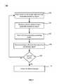
- FIG. 1is a flowchart illustrating selected steps for forming silicon oxide dielectric layers according to disclosed embodiments.
- FIG. 2Ais a chemical schematic of a silicon-and-oxygen-containing molecule for use in atomic layer deposition according to disclosed embodiments.
- FIG. 2Bis a chemical schematic of a silicon-and-oxygen-containing molecule for use in atomic layer deposition according to disclosed embodiments.
- FIG. 2Cis a chemical schematic of a step in an atomic layer deposition process according to disclosed embodiments.
- FIG. 2Dis a chemical schematic of a termination step in an atomic layer deposition process according to disclosed embodiments.
- FIG. 3Ais a chemical schematic of catalytic ligands and optional hydrocarbon chains in silicon-and-oxygen-containing molecules for use in atomic layer deposition according to disclosed embodiments.
- FIG. 3Bis a chemical schematic of a step in an atomic layer deposition process according to disclosed embodiments.
- a deposition precursorcontains silicon, oxygen and a catalytic ligand.
- a hydroxyl-terminated substrateis exposed to the deposition precursor to form a silicon bridge bond between two surface-bound oxygens.
- the surface-bound oxygenswere part of two surface-bound hydroxyl groups and the adsorption of the deposition precursor liberates the hydrogens.
- the silicon atomis also chemically-bound to one or two additional oxygen atoms which were already chemically-bound to the silicon within a same deposition precursor molecule. At least one of the additional oxygen atoms is further chemically-bound to the catalytic ligand either directly or by way of a hydrocarbon chain.
- FIGS. 1-2are a flowchart showing exemplary selected steps for performing atomic layer deposition and chemical schematics during the deposition according to embodiments of the invention.
- the method 100includes flowing a precursor which includes pyrimidine siloxane (H(CH 2 ) n O-pyrimidine, see FIG. 2A ) into a substrate processing region containing a substrate (step 102 ).
- pyrimidine siloxaneH(CH 2 ) n O-pyrimidine, see FIG. 2A
- Siloxane and akloxysilaneare interchangeably used herein and, as such, pyrimidine siloxane may also be referred to as pyrimidine alkoxysilane.
- the substrateis terminated with hydroxyl groups prior to the introduction of the pyrimidine siloxane.
- the pyrimidineis a nitrogen-containing catalytic ligand, in disclosed embodiments, and an alternative representation of pyrimidine siloxane is shown in FIG. 2B .
- a silicon-and-oxygen-containing precursormay be used for this step and the silicon-and-oxygen-containing precursor may be pyrimidine siloxane in disclosed embodiments.
- the silicon-and-oxygen-containing molecules of the silicon-and-oxygen-containing precursormay each contain four oxygen atoms chemically-bound to one silicon atom. Three of the oxygen atoms may each be chemically-bound to a separate hydrocarbon chain and the remaining oxygen atom may be chemically-bound to the catalytic ligand either directly or through a hydrocarbon chain in embodiments of the invention.
- the hydrocarbon chainsmay have the same or different lengths. The lengths of one, some or all the hydrocarbon chains may be zero in embodiments.
- a bridge-bondis formed between two surface-bound oxygen atoms by the silicon atom in the precursor.
- the two hydrogens from the two hydroxyl groupsare liberated along with several process effluents.
- One hydrocarbon chainremains on the surface-bound structure.
- the nitrogen-containing catalytic ligandis also chemically bound to the surface via an oxygen atom (see inset of FIG. 2C ).
- Exposing the substrate to pyrimidine siloxaneis a self-limiting step in embodiments, meaning further exposure to pyrimidine siloxane beyond a certain point makes essentially no further chemical change to the surface.
- the deposition amountplateaus after a period of time in a self-limiting process like this.
- Unreacted pyrimidine siloxane and other process effluentsare removed from the substrate processing region in step 104 .
- the process effluentsmay be removed by flowing inert species into the substrate processing region to flush the process effluents away from the processing region.
- the process effluentsmay be pumped away through a pumping port to a pumping system.
- step 106moisture (H 2 O) is flowed into the substrate processing region (step 106 ) to perform the next step in atomic layer deposition.
- a water molecule (H 2 O) impacting the surfaceinteracts with a nitrogen in the pyrimidine adsorbed on the surface of the substrate (see FIG. 2C ). The interaction allows the water to cleave the Si—O bond of below the hydrocarbon chain (the one without the catalytic ligand attached). Cleavage of the Si—O bond liberates a hydrocarbon chain having an attached hydroxyl group. The reaction forms a bond between the silicon bridge atom and the oxygen of the water.
- a second water moleculeinteracts with one or both of the nitrogen atoms in the catalytic ligand, resulting in cleavage of the Si—O bond affiliated with the same catalytic ligand which enabled the reaction.
- the interactionliberates the catalytic ligand and its hydrocarbon chain as a process effluent.
- the open bonding site created by the liberationis then occupied by a hydroxyl group from the second water molecule.
- Exposing the substrate to moistureis a self-limiting step in embodiments, meaning further exposure to H 2 O beyond a certain point makes essentially no further chemical change to the surface.
- Process effluents including unreacted H 2 Oare removed from the substrate processing region in step 108 .
- the process effluentsmay be removed by flowing inert species into the substrate processing region to flush the process effluents away from the processing region. Alternatively or in combination, the process effluents may be pumped away through a pumping port to a pumping system.
- the four sequential steps(steps 102 - 108 ) can be repeated until a target thickness is achieved (decision 109 ).
- the deposition sequencecomprising the repeated application of the four sequential steps produces a silicon oxide layer on the substrate.
- the last hydroxyl-terminated surfacecan be treated to cross-link the oxygens and liberate hydrogen (step 110 ). This can be done in a variety of ways including heating or exposing the hydroxyl-terminated surface to an oxygen-plasma.
- the cross-linkingis depicted schematically in FIG. 2D .
- the atomic layer deposition process discussed in conjunction with FIGS. 1-2results in high efficiency since the catalytic agent is incorporated on the deposition precursor. This greatly increases the probability that a catalytic agent will be nearby (available) to facilitate the chemical incorporation of a hydroxyl group from the moisture (H 2 O). This increased efficiency enables lower substrate temperatures and pressures to be used during both flowing the silicon-and-oxygen-containing precursor (i.e. the pyrimidine siloxane) and the moisture (H 2 O). Reduced pressure not only decreases the amount of precursor needed to perform the reaction, it also increases the speed with which process effluents may be removed from the substrate processing region.
- a cycle of atomic layer deposition(steps 102 - 108 ) lasts less than 2 seconds in disclosed embodiments. The increased efficiency also allows additional material to be deposited within each cycle compared to atomic layer deposition cycles performed without an embedded catalyst.
- a cycle of atomic layer deposition(four sequential steps 102 - 108 ) deposits more than 1 ⁇ , less than 6 ⁇ or between 1 ⁇ and 6 ⁇ of silicon oxide on the substrate in disclosed embodiments.
- the pressure within the substrate processing regionis below 10 mTorr during one or both of the steps of flowing the silicon-and-oxygen-containing precursor and flowing the moisture (H 2 O) in disclosed embodiments.
- the substrate temperaturemay be less than 200° C. during both of the steps of flowing the silicon-and-oxygen-containing precursor and flowing the moisture (H 2 O) in embodiments of the invention.
- Exemplary catalytic ligandsare represented along with optional hydrocarbon chains in chemical schematics in FIG. 3A .
- Exemplary catalytic ligandsinclude amine, imidazole, alkyl pyridine, pyridine, pyrimidine (as discussed above), pyrrolidine, pyrrole and pyrazole, in disclosed embodiments.
- Each of these catalytic ligandscontains at least one nitrogen and several have more.
- Most of these catalytic ligandscontain a carbon-nitrogen ring which may be referred to as an aromatic carbon-nitrogen ring.
- a carbon-nitrogen ringmay facilitate the catalysis of the Si—O bond of the bridge-bonded silicon.
- a supplementary example involving the imidazole catalytic ligandis shown in FIG. 3B .
- the nitrogen in the aromatic carbon-nitrogen ringenables an incoming water molecule to cleave one of the Si—O bonds (the schematic indicates the Si—O on the left is broken—not necessarily the case). Cleavage of the Si—O bond liberates a hydroxyl-hydrocarbon chain molecule and forms a bond between the silicon bridge atom and the oxygen of the water.
- FIG. 3Binstead of a pyrimidine catalytic ligand ( FIG.
- the second water moleculemay be more easily catalyzed by a nitrogen from an imidazole catalytic ligand chemically-bound to a neighboring oxygen bridge site.
- Each of the catalytic ligandsprovide varying kinetic rates of reaction but all offer favorable deposition rates compared to the use of a separate catalyzer due to the embedded nature of the catalytic ligand.
- Hydrocarbon chainsmay or may not be present on each of the four oxygens of a self-catalyzing silicon-and-oxygen-containing precursor according to embodiments of the invention.
- Exemplary hydrocarbon chainsinclude H(H 2 C) n with n being any positive integer or zero. Therefore, the hydrocarbon chains may include H, CH 3 , C 2 H 5 , C 3 H 7 and so on.
- the hydrocarbon chainsmay have only single bonds and n may range from 0 to 5 in embodiments of the invention.
- the catalytic ligandmay be attached to a siloxane directly or by way of a hydrocarbon chain of the form (H 2 C) n .
- hydrocarbon chainin cases where n is greater than zero, is not included as part of catalytic ligand (“R”) for the purposes of describing the chemical reaction.
- the hydrocarbon chain attaching the oxygen to the catalytic ligandmay be referred to herein as a hydrocarbon extension and may also range from 0 to 5 in embodiments of the invention.
- the hydrocarbon extensionsmay include no extension, CH 2 , C 2 H 4 , C 3 H 6 and so on.
- substratemay be a support substrate with or without layers formed thereon.
- the support substratemay be an insulator or a semiconductor of a variety of doping concentrations and profiles and may, for example, be a semiconductor substrate of the type used in the manufacture of integrated circuits.
- a layer of “silicon oxide”is used as a shorthand for and interchangeably with a silicon-and-oxygen-containing material.
- silicon oxidemay include concentrations of other elemental constituents such as nitrogen, hydrogen, carbon and the like.
- silicon oxideconsists essentially of silicon and oxygen.
- precursoris used to refer to any process gas which takes part in a reaction to either remove material from or deposit material onto a surface.
- a gas in an “excited state”describes a gas wherein at least some of the gas molecules are in vibrationally-excited, dissociated and/or ionized states.
- a “gas”(or a “precursor”) may be a combination of two or more gases (or “precursors”) and may include substances which are normally liquid or solid but temporarily carried along with other “carrier gases.”
- inert gasrefers to any gas which does not form chemical bonds when etching or being incorporated into a film.
- Exemplary inert gasesinclude noble gases but may include other gases so long as no chemical bonds are formed when (typically) trace amounts are trapped in a film.
- trenchis used throughout with no implication that the etched geometry has a large horizontal aspect ratio. Viewed from above the surface, trenches may appear circular, oval, polygonal, rectangular, or a variety of other shapes.
- viais used to refer to a low aspect ratio trench (as viewed from above) which may or may not be filled with metal to form a vertical electrical connection.
- a conformal layerrefers to a generally uniform layer of material on a surface in the same shape as the surface, i.e., the surface of the layer and the surface being covered are generally parallel. A person having ordinary skill in the art will recognize that the deposited material likely cannot be 100% conformal and thus the term “generally” allows for acceptable tolerances.
Landscapes
- Chemical & Material Sciences (AREA)
- Engineering & Computer Science (AREA)
- Physics & Mathematics (AREA)
- Condensed Matter Physics & Semiconductors (AREA)
- Power Engineering (AREA)
- Microelectronics & Electronic Packaging (AREA)
- Chemical Kinetics & Catalysis (AREA)
- Computer Hardware Design (AREA)
- Manufacturing & Machinery (AREA)
- General Physics & Mathematics (AREA)
- Materials Engineering (AREA)
- Organic Chemistry (AREA)
- Metallurgy (AREA)
- Mechanical Engineering (AREA)
- General Chemical & Material Sciences (AREA)
- Spectroscopy & Molecular Physics (AREA)
- Inorganic Chemistry (AREA)
- Plasma & Fusion (AREA)
- Chemical Vapour Deposition (AREA)
- Formation Of Insulating Films (AREA)
- Silicon Compounds (AREA)
Abstract
Description
- This application claims the benefit of U.S. Provisional Patent Application No. 61/381,889 filed Sep. 10, 2010, and titled “EMBEDDED CATALYST FOR ATOMIC LAYER DEPOSITION OF SILICON OXIDE,” which is incorporated herein by reference in its entirety for all purposes.
- Silicon oxide dielectric films form resilient interfaces with silicon and provide high dielectric strength and a relatively low dielectric constant. These traits result in heavy use of silicon oxide for insulating electrically active features from one another. Two conventional methods for depositing a silicon oxide film include: (1) oxidation process wherein silicon is oxidized at relatively high temperatures (e.g., sometimes more than 1000° C.); and (2) a chemical vapor deposition (CVD) process wherein the silicon and oxygen sources are introduced into a chamber and exposed to energy (e.g., heat) to form a silicon oxide film. Silicon oxide CVD processes typically occur at temperatures ranging from 600° C. to 800° C. or below 450° C. depending on the application. While satisfactory for larger integrated circuit linewidths, these methods can cause diffusion at interfaces due to the high deposition temperature, thereby degrading electrical characteristics of miniature electrical devices.
- In addition to lower substrate temperatures, thin films used in semiconductor devices will increasingly require atomic layer control during deposition due to the decreasing linewidths. These thin films will also be required to have excellent step coverage and conformality. To satisfy the requirements, atomic layer deposition (ALD) process have gained traction in semiconductor manufacturing.
- ALD silicon oxide films have been deposited at a temperature of more than 600K via the atomic layer deposition process using SiCl4and H2O sources. In this exemplary prior art process, a SiCl4source is provided in a substrate processing region containing a substrate having hydroxyl groups (—OH) on its surface. The SiCl4source reacts with the hydroxyl group in this first deposition step, and —SiCl3is adsorbed on the surface of the substrate, HCl by-products are formed. When the reaction of SiCl4with the hydroxyl group is essentially complete, a monolayer of Si has been added to the surface of the substrate. Further exposure to SiCl4results in insignificant additional deposition. Such a reaction is referred to as self-limiting. At this point, the surface of the substrate is terminated with —SiCl3surface chemical species.
- An H2O source is then flowed into the substrate processing region. H2O reacts with the —SiCl3surface chemical species to generate adsorption of the hydroxyl group thereto and HCl by-products. A monolayer of oxygen has now been added on top of the previously deposited monolayer of silicon. This second deposition step is also self-limiting; further exposure to H2O results in little additional deposition. These two deposition steps may be repeated to deposit a silicon oxide film having a desired thickness. This prior art deposition method is limited to relatively high substrate temperature and low growth rates.
- A catalyst, e.g. pyridine, may be introduced sequentially, following exposure of the surface to the silicon source described above in order to facilitate deposition at lower substrate temperatures. ALD has been performed in this way at substrate temperatures below 200° C. Introducing an additional step, however, further reduces the already low deposition rate. Concurrent exposure to multiple deposition precursors does not significantly address the low growth and sacrifices the atomic layer control desired for most ALD processes. Furthermore, the presence of chlorine and ammonia in the effluents produces undesirable salts which can incorporate into the depositing film in addition to requiring specialized deposition chamber cleaning procedures. Alternative silicon precursors which do not contain chlorine address the production of undesirable salts but do not address the low growth rates.
- Thus, there remains a need for new atomic layer deposition processes and materials to form relatively pure dielectric materials at low temperatures but increased growth rates. This and other needs are addressed in the present application.
- Catalyzed atomic layer deposition from a reduced number of precursors is described. A deposition precursor contains silicon, oxygen and a catalytic ligand. A hydroxyl-terminated substrate is exposed to the deposition precursor to form a silicon bridge bond between two surface-bound oxygens. The surface-bound oxygens were part of two surface-bound hydroxyl groups and the adsorption of the deposition precursor liberates the hydrogens. The silicon atom is also chemically-bound to one or two additional oxygen atoms which were already chemically-bound to the silicon within a same deposition precursor molecule. At least one of the additional oxygen atoms is further chemically-bound to the catalytic ligand either directly or by way of a hydrocarbon chain. Further exposure of the substrate to moisture (H2O) results in displacement of the additional oxygen which are replaced by hydroxyl groups from the moisture. The surface is again hydroxyl-terminated and the process may be repeated. The catalytic nature of the reaction enables the deposition to occur at low substrate temperatures. The chemically-embedded nature of the catalyst increases the deposition per cycle thereby reducing the number of precursor exposures to grow a film of the same thickness.
- Embodiments of the invention include methods of forming a silicon oxide layer on a hydroxyl-terminated surface of a substrate positioned in a substrate processing region. The methods include at least four sequential steps: (i) exposing the hydroxyl-terminated surface to a silicon-and-oxygen-containing precursor comprising a siloxane and a nitrogen-containing catalytic ligand by flowing the silicon-and-oxygen-containing precursor into the substrate processing region, (ii) removing process effluents including unreacted silicon-and-oxygen-containing precursor from the substrate processing region, (iii) exposing the surface of the substrate by flowing H2O into the substrate processing region, and (iv) removing process effluents including unreacted H2O from the substrate processing region. The methods further include repeating the at least four sequential steps until the silicon oxide layer reaches a target thickness.
- Embodiments of the invention include methods of forming a silicon oxide layer on a hydroxyl-terminated surface of a substrate within a substrate processing region. The methods include performing a cycle of atomic layer deposition comprising the sequential steps: (1) flowing a silicon-and-oxygen-containing precursor containing silicon-and-oxygen-containing molecules into the substrate processing region to form a bridge bonded silicon atom bridging between two surface-bound oxygen adatoms, wherein the two surface-bound oxygen adatoms originated within separate hydroxyl termination groups, and then (2) flowing H2O into the substrate processing region to bind hydroxyl groups to each of the two remaining sites of the bridge-bonded silicon atom. The silicon-and-oxygen-containing molecules further include a catalytic ligand, which enables the H2O to cleave the Si—O bond and further enables a hydroxyl group from the H2O to chemically bind to the cleaved site of the bridge-bonded silicon atom.
- Additional embodiments and features are set forth in part in the description that follows, and in part will become apparent to those skilled in the art upon examination of the specification or may be learned by the practice of the disclosed embodiments. The features and advantages of the disclosed embodiments may be realized and attained by means of the instrumentalities, combinations, and methods described in the specification.
- A further understanding of the nature and advantages of the present invention may be realized by reference to the remaining portions of the specification and the drawings wherein like reference numerals are used throughout the several drawings to refer to similar components. In some instances, a sublabel is associated with a reference numeral and follows a hyphen to denote one of multiple similar components. When reference is made to a reference numeral without specification to an existing sublabel, it is intended to refer to all such multiple similar components.
FIG. 1 is a flowchart illustrating selected steps for forming silicon oxide dielectric layers according to disclosed embodiments.FIG. 2A is a chemical schematic of a silicon-and-oxygen-containing molecule for use in atomic layer deposition according to disclosed embodiments.FIG. 2B is a chemical schematic of a silicon-and-oxygen-containing molecule for use in atomic layer deposition according to disclosed embodiments.FIG. 2C is a chemical schematic of a step in an atomic layer deposition process according to disclosed embodiments.FIG. 2D is a chemical schematic of a termination step in an atomic layer deposition process according to disclosed embodiments.FIG. 3A is a chemical schematic of catalytic ligands and optional hydrocarbon chains in silicon-and-oxygen-containing molecules for use in atomic layer deposition according to disclosed embodiments.FIG. 3B is a chemical schematic of a step in an atomic layer deposition process according to disclosed embodiments.- Catalyzed atomic layer deposition from a reduced number of precursors is described. A deposition precursor contains silicon, oxygen and a catalytic ligand. A hydroxyl-terminated substrate is exposed to the deposition precursor to form a silicon bridge bond between two surface-bound oxygens. The surface-bound oxygens were part of two surface-bound hydroxyl groups and the adsorption of the deposition precursor liberates the hydrogens. The silicon atom is also chemically-bound to one or two additional oxygen atoms which were already chemically-bound to the silicon within a same deposition precursor molecule. At least one of the additional oxygen atoms is further chemically-bound to the catalytic ligand either directly or by way of a hydrocarbon chain. Further exposure of the substrate to moisture (H2O) results in displacement of the additional oxygen which are replaced by hydroxyl groups from the moisture. The surface is again hydroxyl-terminated and the process may be repeated. The catalytic nature of the reaction enables the deposition to occur at low substrate temperatures. The chemically-embedded nature of the catalyst increases the deposition per cycle thereby reducing the number of precursor exposures to grow a film of the same thickness.
- In order to better understand and appreciate the invention, reference is now made to
FIGS. 1-2 which are a flowchart showing exemplary selected steps for performing atomic layer deposition and chemical schematics during the deposition according to embodiments of the invention. Themethod 100 includes flowing a precursor which includes pyrimidine siloxane (H(CH2)nO-pyrimidine, seeFIG. 2A ) into a substrate processing region containing a substrate (step102). Siloxane and akloxysilane are interchangeably used herein and, as such, pyrimidine siloxane may also be referred to as pyrimidine alkoxysilane. The substrate is terminated with hydroxyl groups prior to the introduction of the pyrimidine siloxane. The pyrimidine is a nitrogen-containing catalytic ligand, in disclosed embodiments, and an alternative representation of pyrimidine siloxane is shown inFIG. 2B . Generally speaking, a silicon-and-oxygen-containing precursor may be used for this step and the silicon-and-oxygen-containing precursor may be pyrimidine siloxane in disclosed embodiments. The silicon-and-oxygen-containing molecules of the silicon-and-oxygen-containing precursor may each contain four oxygen atoms chemically-bound to one silicon atom. Three of the oxygen atoms may each be chemically-bound to a separate hydrocarbon chain and the remaining oxygen atom may be chemically-bound to the catalytic ligand either directly or through a hydrocarbon chain in embodiments of the invention. The hydrocarbon chains may have the same or different lengths. The lengths of one, some or all the hydrocarbon chains may be zero in embodiments. As the pyrimidine siloxane approaches the hydroxyl-terminated substrate, a bridge-bond is formed between two surface-bound oxygen atoms by the silicon atom in the precursor. The two hydrogens from the two hydroxyl groups are liberated along with several process effluents. One hydrocarbon chain remains on the surface-bound structure. The nitrogen-containing catalytic ligand is also chemically bound to the surface via an oxygen atom (see inset ofFIG. 2C ). Exposing the substrate to pyrimidine siloxane is a self-limiting step in embodiments, meaning further exposure to pyrimidine siloxane beyond a certain point makes essentially no further chemical change to the surface. The deposition amount plateaus after a period of time in a self-limiting process like this. - Unreacted pyrimidine siloxane and other process effluents are removed from the substrate processing region in
step 104. The process effluents may be removed by flowing inert species into the substrate processing region to flush the process effluents away from the processing region. Alternatively or in combination, the process effluents may be pumped away through a pumping port to a pumping system. - At this point, a catalytic exposure would have been needed if catalytic ligands were not present in the deposition precursor. Instead, moisture (H2O) is flowed into the substrate processing region (step106) to perform the next step in atomic layer deposition. A water molecule (H2O) impacting the surface interacts with a nitrogen in the pyrimidine adsorbed on the surface of the substrate (see
FIG. 2C ). The interaction allows the water to cleave the Si—O bond of below the hydrocarbon chain (the one without the catalytic ligand attached). Cleavage of the Si—O bond liberates a hydrocarbon chain having an attached hydroxyl group. The reaction forms a bond between the silicon bridge atom and the oxygen of the water. Meanwhile a second water molecule interacts with one or both of the nitrogen atoms in the catalytic ligand, resulting in cleavage of the Si—O bond affiliated with the same catalytic ligand which enabled the reaction. The interaction liberates the catalytic ligand and its hydrocarbon chain as a process effluent. The open bonding site created by the liberation is then occupied by a hydroxyl group from the second water molecule. Exposing the substrate to moisture is a self-limiting step in embodiments, meaning further exposure to H2O beyond a certain point makes essentially no further chemical change to the surface. - Process effluents including unreacted H2O are removed from the substrate processing region in
step 108. The process effluents may be removed by flowing inert species into the substrate processing region to flush the process effluents away from the processing region. Alternatively or in combination, the process effluents may be pumped away through a pumping port to a pumping system. The four sequential steps (steps102-108) can be repeated until a target thickness is achieved (decision109). The deposition sequence comprising the repeated application of the four sequential steps produces a silicon oxide layer on the substrate. - Once the target thickness is achieved, the last hydroxyl-terminated surface can be treated to cross-link the oxygens and liberate hydrogen (step110). This can be done in a variety of ways including heating or exposing the hydroxyl-terminated surface to an oxygen-plasma. The cross-linking is depicted schematically in
FIG. 2D . - The atomic layer deposition process discussed in conjunction with
FIGS. 1-2 results in high efficiency since the catalytic agent is incorporated on the deposition precursor. This greatly increases the probability that a catalytic agent will be nearby (available) to facilitate the chemical incorporation of a hydroxyl group from the moisture (H2O). This increased efficiency enables lower substrate temperatures and pressures to be used during both flowing the silicon-and-oxygen-containing precursor (i.e. the pyrimidine siloxane) and the moisture (H2O). Reduced pressure not only decreases the amount of precursor needed to perform the reaction, it also increases the speed with which process effluents may be removed from the substrate processing region. A cycle of atomic layer deposition (steps102-108) lasts less than 2 seconds in disclosed embodiments. The increased efficiency also allows additional material to be deposited within each cycle compared to atomic layer deposition cycles performed without an embedded catalyst. A cycle of atomic layer deposition (four sequential steps102-108) deposits more than 1 Å, less than 6 Å or between 1 Å and 6 Å of silicon oxide on the substrate in disclosed embodiments. The pressure within the substrate processing region is below 10 mTorr during one or both of the steps of flowing the silicon-and-oxygen-containing precursor and flowing the moisture (H2O) in disclosed embodiments. The substrate temperature may be less than 200° C. during both of the steps of flowing the silicon-and-oxygen-containing precursor and flowing the moisture (H2O) in embodiments of the invention. - The benefits and process parameters described above extend to a wider variety of silicon-and-oxygen-containing precursors than pyrimidine siloxane. Exemplary catalytic ligands are represented along with optional hydrocarbon chains in chemical schematics in
FIG. 3A . Exemplary catalytic ligands include amine, imidazole, alkyl pyridine, pyridine, pyrimidine (as discussed above), pyrrolidine, pyrrole and pyrazole, in disclosed embodiments. Each of these catalytic ligands contains at least one nitrogen and several have more. Most of these catalytic ligands contain a carbon-nitrogen ring which may be referred to as an aromatic carbon-nitrogen ring. A carbon-nitrogen ring may facilitate the catalysis of the Si—O bond of the bridge-bonded silicon. A supplementary example involving the imidazole catalytic ligand is shown inFIG. 3B . The nitrogen in the aromatic carbon-nitrogen ring enables an incoming water molecule to cleave one of the Si—O bonds (the schematic indicates the Si—O on the left is broken—not necessarily the case). Cleavage of the Si—O bond liberates a hydroxyl-hydrocarbon chain molecule and forms a bond between the silicon bridge atom and the oxygen of the water. Using an imidazole catalytic ligand (FIG. 3B ) instead of a pyrimidine catalytic ligand (FIG. 2C ) may have different kinetic behavior since the second water molecule (H2O) may be more easily catalyzed by a nitrogen from an imidazole catalytic ligand chemically-bound to a neighboring oxygen bridge site. Each of the catalytic ligands provide varying kinetic rates of reaction but all offer favorable deposition rates compared to the use of a separate catalyzer due to the embedded nature of the catalytic ligand. - Hydrocarbon chains may or may not be present on each of the four oxygens of a self-catalyzing silicon-and-oxygen-containing precursor according to embodiments of the invention. Exemplary hydrocarbon chains include H(H2C)nwith n being any positive integer or zero. Therefore, the hydrocarbon chains may include H, CH3, C2H5, C3H7and so on. The hydrocarbon chains may have only single bonds and n may range from 0 to 5 in embodiments of the invention. As indicated previously, the catalytic ligand may be attached to a siloxane directly or by way of a hydrocarbon chain of the form (H2C)n. The hydrocarbon chain, in cases where n is greater than zero, is not included as part of catalytic ligand (“R”) for the purposes of describing the chemical reaction. The hydrocarbon chain attaching the oxygen to the catalytic ligand may be referred to herein as a hydrocarbon extension and may also range from 0 to 5 in embodiments of the invention. As such, the hydrocarbon extensions may include no extension, CH2, C2H4, C3H6and so on.
- As used herein “substrate” may be a support substrate with or without layers formed thereon. The support substrate may be an insulator or a semiconductor of a variety of doping concentrations and profiles and may, for example, be a semiconductor substrate of the type used in the manufacture of integrated circuits. A layer of “silicon oxide” is used as a shorthand for and interchangeably with a silicon-and-oxygen-containing material. As such, silicon oxide may include concentrations of other elemental constituents such as nitrogen, hydrogen, carbon and the like. In some embodiments, silicon oxide consists essentially of silicon and oxygen. The term “precursor” is used to refer to any process gas which takes part in a reaction to either remove material from or deposit material onto a surface. A gas in an “excited state” describes a gas wherein at least some of the gas molecules are in vibrationally-excited, dissociated and/or ionized states. A “gas” (or a “precursor”) may be a combination of two or more gases (or “precursors”) and may include substances which are normally liquid or solid but temporarily carried along with other “carrier gases.” The phrase “inert gas” refers to any gas which does not form chemical bonds when etching or being incorporated into a film. Exemplary inert gases include noble gases but may include other gases so long as no chemical bonds are formed when (typically) trace amounts are trapped in a film.
- The term “trench” is used throughout with no implication that the etched geometry has a large horizontal aspect ratio. Viewed from above the surface, trenches may appear circular, oval, polygonal, rectangular, or a variety of other shapes. The term “via” is used to refer to a low aspect ratio trench (as viewed from above) which may or may not be filled with metal to form a vertical electrical connection. As used herein, a conformal layer refers to a generally uniform layer of material on a surface in the same shape as the surface, i.e., the surface of the layer and the surface being covered are generally parallel. A person having ordinary skill in the art will recognize that the deposited material likely cannot be 100% conformal and thus the term “generally” allows for acceptable tolerances.
- Having described several embodiments, it will be recognized by those of skill in the art that various modifications, alternative constructions, and equivalents may be used without departing from the spirit of the invention. Additionally, a number of well-known processes and elements have not been described in order to avoid unnecessarily obscuring the present invention. Accordingly, the above description should not be taken as limiting the scope of the invention.
- Where a range of values is provided, it is understood that each intervening value, to the tenth of the unit of the lower limit unless the context clearly dictates otherwise, between the upper and lower limits of that range is also specifically disclosed. Each smaller range between any stated value or intervening value in a stated range and any other stated or intervening value in that stated range is encompassed. The upper and lower limits of these smaller ranges may independently be included or excluded in the range, and each range where either, neither or both limits are included in the smaller ranges is also encompassed within the invention, subject to any specifically excluded limit in the stated range. Where the stated range includes one or both of the limits, ranges excluding either or both of those included limits are also included.
- As used herein and in the appended claims, the singular forms “a”, “an”, and “the” include plural referents unless the context clearly dictates otherwise. Thus, for example, reference to “a process” includes a plurality of such processes and reference to “the precursor” includes reference to one or more precursor and equivalents thereof known to those skilled in the art, and so forth.
- Also, the words “comprise,” “comprising,” “include,” “including,” and “includes” when used in this specification and in the following claims are intended to specify the presence of stated features, integers, components, or steps, but they do not preclude the presence or addition of one or more other features, integers, components, steps, acts, or groups.
Claims (20)
1. A method of forming a silicon oxide layer on a hydroxyl-terminated surface of a substrate positioned in a substrate processing region, the method comprising:
at least four sequential steps comprising:
(i) exposing the hydroxyl-terminated surface to a silicon-and-oxygen-containing precursor comprising a siloxane and a nitrogen-containing catalytic ligand by flowing the silicon-and-oxygen-containing precursor into the substrate processing region,
(ii) removing process effluents including unreacted silicon-and-oxygen-containing precursor from the substrate processing region,
(iii) exposing the surface of the substrate by flowing H2O into the substrate processing region, and
(iv) removing process effluents including unreacted H2O from the substrate processing region; and
repeating the at least four sequential steps until the silicon oxide layer reaches a target thickness.
2. The method ofclaim 1 , wherein each iteration of steps (i)-(iv) deposits between 1 Å and 6 Å of silicon oxide on the substrate.
3. The method ofclaim 1 , wherein the nitrogen-containing catalytic ligand comprises a carbon-nitrogen ring.
4. The method ofclaim 1 , wherein the silicon-and-oxygen-containing molecules each contain four oxygen atoms chemically-bound to one silicon atom, wherein three of the oxygen atoms are each chemically-bound to a separate hydrocarbon chain and the remaining oxygen atom is chemically-bound to the catalytic ligand.
5. The method ofclaim 1 , wherein the catalytic ligand comprises a carbon-nitrogen ring.
6. The method ofclaim 1 , wherein the catalytic ligand is chemically-bound to a hydrocarbon extension and the hydrocarbon extension is chemically-bound to an oxygen atom in the siloxane.
7. The method ofclaim 1 , wherein the catalytic ligand comprises one nitrogen atom and either 4 or 5 carbon atoms arranged in a carbon-nitrogen ring.
8. The method ofclaim 1 , wherein the catalytic ligand comprises two nitrogen atoms and either 3 or 4 carbon atoms arranged in a carbon-nitrogen ring.
9. The method ofclaim 1 , wherein the silicon-and-oxygen-containing precursor comprises pyrimidine-alkoxysilane.
10. The method ofclaim 1 , wherein the catalytic ligand comprises one of Pyrimidine, Imidazole, Amine, Alkyl Pyridine, Pyridine, Pyrrolidine, Pyrrole or Pyrazole.
11. The method ofclaim 1 , wherein the pressure within the substrate processing region is below 10 mTorr during one of flowing the silicon-and-oxygen-containing precursor and flowing the H2O.
12. The method ofclaim 1 , wherein a temperature of the substrate is below 200° C. during each of flowing the silicon-and-oxygen-containing precursor and flowing the H2O.
13. The method ofclaim 1 , wherein one of the plurality of cycles of atomic layer deposition lasts for 2 seconds or less.
14. The method ofclaim 1 , wherein the substrate is a patterned substrate having a trench with a width of about 25 nm or less.
15. A method of forming a silicon oxide layer on a hydroxyl-terminated surface of a substrate within a substrate processing region, the method comprising:
performing a plurality of cycles of atomic layer deposition, each cycle comprising the sequential steps:
(1) flowing a silicon-and-oxygen-containing precursor containing silicon-and-oxygen-containing molecules into the substrate processing region to form a bridge bonded silicon atom bridging between two surface-bound oxygen adatoms, wherein the two surface-bound oxygen adatoms originated within separate hydroxyl termination groups, and then
(2) flowing H2O into the substrate processing region to bind hydroxyl groups to each of the two remaining sites of the bridge-bonded silicon atom,
wherein the silicon-and-oxygen-containing molecules further comprise a catalytic ligand, which enables the H2O to cleave the Si—O bond and further enables a hydroxyl group from the H2O to chemically bind to the cleaved site of the bridge-bonded silicon atom.
16. The method ofclaim 15 , wherein one of the plurality of cycles of atomic layer deposition deposits between 1 Å and 6 Å of silicon oxide on the substrate.
17. The method ofclaim 15 , further comprising selecting an integral number of the plurality of cycles to achieve a target thickness of the silicon oxide layer.
18. The method ofclaim 15 , further comprising cross-linking the last hydroxyl-terminated surface by heating the substrate or exposing the substrate to an oxygen plasma to produce a bridge bonded oxygen.
19. The method ofclaim 15 , wherein the catalytic ligand which enables a hydroxyl group to bind to the first bridge-bonded silicon atom is chemically-bound to a second bridge-bonded silicon atom, nearby but different from the first.
20. The method ofclaim 15 , wherein the catalytic ligand which enables a hydroxyl group to bind to the first bridge-bonded silicon atom is chemically-bound to the first bridge-bonded silicon atom.
Priority Applications (7)
| Application Number | Priority Date | Filing Date | Title |
|---|---|---|---|
| US13/197,517US8580699B2 (en) | 2010-09-10 | 2011-08-03 | Embedded catalyst for atomic layer deposition of silicon oxide |
| SG2013016027ASG188388A1 (en) | 2010-09-10 | 2011-09-02 | Embedded catalyst for atomic layer deposition of silicon oxide |
| KR1020137009063AKR101903949B1 (en) | 2010-09-10 | 2011-09-02 | Embedded catalyst for atomic layer deposition of silicon oxide |
| PCT/US2011/050391WO2012033717A2 (en) | 2010-09-10 | 2011-09-02 | Embedded catalyst for atomic layer deposition of silicon oxide |
| CN2011800446924ACN103109358A (en) | 2010-09-10 | 2011-09-02 | Embedded catalyst for atomic layer deposition of silicon oxide |
| JP2013528240AJP2013538008A (en) | 2010-09-10 | 2011-09-02 | Embedded catalyst for atomic layer deposition of silicon oxide |
| TW100132765ATW201213592A (en) | 2010-09-10 | 2011-09-09 | Embedded catalyst for atomic layer deposition of silicon oxide |
Applications Claiming Priority (2)
| Application Number | Priority Date | Filing Date | Title |
|---|---|---|---|
| US38188910P | 2010-09-10 | 2010-09-10 | |
| US13/197,517US8580699B2 (en) | 2010-09-10 | 2011-08-03 | Embedded catalyst for atomic layer deposition of silicon oxide |
Publications (2)
| Publication Number | Publication Date |
|---|---|
| US20120196451A1true US20120196451A1 (en) | 2012-08-02 |
| US8580699B2 US8580699B2 (en) | 2013-11-12 |
Family
ID=45811127
Family Applications (1)
| Application Number | Title | Priority Date | Filing Date |
|---|---|---|---|
| US13/197,517Active2032-01-24US8580699B2 (en) | 2010-09-10 | 2011-08-03 | Embedded catalyst for atomic layer deposition of silicon oxide |
Country Status (7)
| Country | Link |
|---|---|
| US (1) | US8580699B2 (en) |
| JP (1) | JP2013538008A (en) |
| KR (1) | KR101903949B1 (en) |
| CN (1) | CN103109358A (en) |
| SG (1) | SG188388A1 (en) |
| TW (1) | TW201213592A (en) |
| WO (1) | WO2012033717A2 (en) |
Cited By (88)
| Publication number | Priority date | Publication date | Assignee | Title |
|---|---|---|---|---|
| US20150145041A1 (en)* | 2013-11-22 | 2015-05-28 | International Business Machines Corporation | Substrate local interconnect integration with finfets |
| KR20160130165A (en)* | 2015-05-01 | 2016-11-10 | 어플라이드 머티어리얼스, 인코포레이티드 | Selective deposition of thin film dielectrics using surface blocking chemistry |
| US9508545B2 (en)* | 2015-02-09 | 2016-11-29 | Applied Materials, Inc. | Selectively lateral growth of silicon oxide thin film |
| WO2018089536A1 (en)* | 2016-11-11 | 2018-05-17 | Applied Materials, Inc. | Removal methods for high aspect ratio structures |
| US10026621B2 (en) | 2016-11-14 | 2018-07-17 | Applied Materials, Inc. | SiN spacer profile patterning |
| US10032606B2 (en) | 2012-08-02 | 2018-07-24 | Applied Materials, Inc. | Semiconductor processing with DC assisted RF power for improved control |
| US10043674B1 (en) | 2017-08-04 | 2018-08-07 | Applied Materials, Inc. | Germanium etching systems and methods |
| US10043684B1 (en) | 2017-02-06 | 2018-08-07 | Applied Materials, Inc. | Self-limiting atomic thermal etching systems and methods |
| US10049891B1 (en) | 2017-05-31 | 2018-08-14 | Applied Materials, Inc. | Selective in situ cobalt residue removal |
| US10062575B2 (en) | 2016-09-09 | 2018-08-28 | Applied Materials, Inc. | Poly directional etch by oxidation |
| US10062585B2 (en) | 2016-10-04 | 2018-08-28 | Applied Materials, Inc. | Oxygen compatible plasma source |
| US10128086B1 (en) | 2017-10-24 | 2018-11-13 | Applied Materials, Inc. | Silicon pretreatment for nitride removal |
| US10147620B2 (en) | 2015-08-06 | 2018-12-04 | Applied Materials, Inc. | Bolted wafer chuck thermal management systems and methods for wafer processing systems |
| US10163696B2 (en) | 2016-11-11 | 2018-12-25 | Applied Materials, Inc. | Selective cobalt removal for bottom up gapfill |
| US10170336B1 (en) | 2017-08-04 | 2019-01-01 | Applied Materials, Inc. | Methods for anisotropic control of selective silicon removal |
| US10192775B2 (en) | 2016-03-17 | 2019-01-29 | Applied Materials, Inc. | Methods for gapfill in high aspect ratio structures |
| US20190067194A1 (en)* | 2017-08-31 | 2019-02-28 | Taiwan Semiconductor Manufacturing Co., Ltd. | Interconnect structure for semiconductor device and methods of fabrication thereof |
| US10224180B2 (en) | 2016-10-04 | 2019-03-05 | Applied Materials, Inc. | Chamber with flow-through source |
| US10224210B2 (en) | 2014-12-09 | 2019-03-05 | Applied Materials, Inc. | Plasma processing system with direct outlet toroidal plasma source |
| US10242908B2 (en) | 2016-11-14 | 2019-03-26 | Applied Materials, Inc. | Airgap formation with damage-free copper |
| US10256079B2 (en) | 2013-02-08 | 2019-04-09 | Applied Materials, Inc. | Semiconductor processing systems having multiple plasma configurations |
| US10256112B1 (en) | 2017-12-08 | 2019-04-09 | Applied Materials, Inc. | Selective tungsten removal |
| US10283324B1 (en) | 2017-10-24 | 2019-05-07 | Applied Materials, Inc. | Oxygen treatment for nitride etching |
| US10283321B2 (en) | 2011-01-18 | 2019-05-07 | Applied Materials, Inc. | Semiconductor processing system and methods using capacitively coupled plasma |
| US10297458B2 (en) | 2017-08-07 | 2019-05-21 | Applied Materials, Inc. | Process window widening using coated parts in plasma etch processes |
| US10319649B2 (en) | 2017-04-11 | 2019-06-11 | Applied Materials, Inc. | Optical emission spectroscopy (OES) for remote plasma monitoring |
| US10319739B2 (en) | 2017-02-08 | 2019-06-11 | Applied Materials, Inc. | Accommodating imperfectly aligned memory holes |
| US10319603B2 (en) | 2016-10-07 | 2019-06-11 | Applied Materials, Inc. | Selective SiN lateral recess |
| US10319600B1 (en) | 2018-03-12 | 2019-06-11 | Applied Materials, Inc. | Thermal silicon etch |
| US10354843B2 (en) | 2012-09-21 | 2019-07-16 | Applied Materials, Inc. | Chemical control features in wafer process equipment |
| US10354889B2 (en) | 2017-07-17 | 2019-07-16 | Applied Materials, Inc. | Non-halogen etching of silicon-containing materials |
| US10403507B2 (en) | 2017-02-03 | 2019-09-03 | Applied Materials, Inc. | Shaped etch profile with oxidation |
| US10424487B2 (en) | 2017-10-24 | 2019-09-24 | Applied Materials, Inc. | Atomic layer etching processes |
| US10424463B2 (en) | 2015-08-07 | 2019-09-24 | Applied Materials, Inc. | Oxide etch selectivity systems and methods |
| US10424485B2 (en) | 2013-03-01 | 2019-09-24 | Applied Materials, Inc. | Enhanced etching processes using remote plasma sources |
| US10431429B2 (en) | 2017-02-03 | 2019-10-01 | Applied Materials, Inc. | Systems and methods for radial and azimuthal control of plasma uniformity |
| US10468276B2 (en) | 2015-08-06 | 2019-11-05 | Applied Materials, Inc. | Thermal management systems and methods for wafer processing systems |
| US10468285B2 (en) | 2015-02-03 | 2019-11-05 | Applied Materials, Inc. | High temperature chuck for plasma processing systems |
| US10465294B2 (en) | 2014-05-28 | 2019-11-05 | Applied Materials, Inc. | Oxide and metal removal |
| US10468267B2 (en) | 2017-05-31 | 2019-11-05 | Applied Materials, Inc. | Water-free etching methods |
| US10490406B2 (en) | 2018-04-10 | 2019-11-26 | Appled Materials, Inc. | Systems and methods for material breakthrough |
| US10490418B2 (en) | 2014-10-14 | 2019-11-26 | Applied Materials, Inc. | Systems and methods for internal surface conditioning assessment in plasma processing equipment |
| US10497573B2 (en) | 2018-03-13 | 2019-12-03 | Applied Materials, Inc. | Selective atomic layer etching of semiconductor materials |
| US10504754B2 (en) | 2016-05-19 | 2019-12-10 | Applied Materials, Inc. | Systems and methods for improved semiconductor etching and component protection |
| US10504700B2 (en) | 2015-08-27 | 2019-12-10 | Applied Materials, Inc. | Plasma etching systems and methods with secondary plasma injection |
| US10522371B2 (en) | 2016-05-19 | 2019-12-31 | Applied Materials, Inc. | Systems and methods for improved semiconductor etching and component protection |
| US10541246B2 (en) | 2017-06-26 | 2020-01-21 | Applied Materials, Inc. | 3D flash memory cells which discourage cross-cell electrical tunneling |
| US10541184B2 (en) | 2017-07-11 | 2020-01-21 | Applied Materials, Inc. | Optical emission spectroscopic techniques for monitoring etching |
| US10546729B2 (en) | 2016-10-04 | 2020-01-28 | Applied Materials, Inc. | Dual-channel showerhead with improved profile |
| US10566206B2 (en) | 2016-12-27 | 2020-02-18 | Applied Materials, Inc. | Systems and methods for anisotropic material breakthrough |
| US10573527B2 (en) | 2018-04-06 | 2020-02-25 | Applied Materials, Inc. | Gas-phase selective etching systems and methods |
| US10573496B2 (en) | 2014-12-09 | 2020-02-25 | Applied Materials, Inc. | Direct outlet toroidal plasma source |
| US10593523B2 (en) | 2014-10-14 | 2020-03-17 | Applied Materials, Inc. | Systems and methods for internal surface conditioning in plasma processing equipment |
| US10593560B2 (en) | 2018-03-01 | 2020-03-17 | Applied Materials, Inc. | Magnetic induction plasma source for semiconductor processes and equipment |
| US10615047B2 (en) | 2018-02-28 | 2020-04-07 | Applied Materials, Inc. | Systems and methods to form airgaps |
| US10629473B2 (en) | 2016-09-09 | 2020-04-21 | Applied Materials, Inc. | Footing removal for nitride spacer |
| US10672642B2 (en) | 2018-07-24 | 2020-06-02 | Applied Materials, Inc. | Systems and methods for pedestal configuration |
| US10679870B2 (en) | 2018-02-15 | 2020-06-09 | Applied Materials, Inc. | Semiconductor processing chamber multistage mixing apparatus |
| US10699879B2 (en) | 2018-04-17 | 2020-06-30 | Applied Materials, Inc. | Two piece electrode assembly with gap for plasma control |
| US10727080B2 (en) | 2017-07-07 | 2020-07-28 | Applied Materials, Inc. | Tantalum-containing material removal |
| US10755941B2 (en) | 2018-07-06 | 2020-08-25 | Applied Materials, Inc. | Self-limiting selective etching systems and methods |
| US10854426B2 (en) | 2018-01-08 | 2020-12-01 | Applied Materials, Inc. | Metal recess for semiconductor structures |
| US10872778B2 (en) | 2018-07-06 | 2020-12-22 | Applied Materials, Inc. | Systems and methods utilizing solid-phase etchants |
| US10872762B2 (en)* | 2017-11-08 | 2020-12-22 | Taiwan Semiconductor Manufacturing Company, Ltd. | Methods of forming silicon oxide layer and semiconductor structure |
| US10886137B2 (en) | 2018-04-30 | 2021-01-05 | Applied Materials, Inc. | Selective nitride removal |
| US10892198B2 (en) | 2018-09-14 | 2021-01-12 | Applied Materials, Inc. | Systems and methods for improved performance in semiconductor processing |
| US10903054B2 (en) | 2017-12-19 | 2021-01-26 | Applied Materials, Inc. | Multi-zone gas distribution systems and methods |
| US10920320B2 (en) | 2017-06-16 | 2021-02-16 | Applied Materials, Inc. | Plasma health determination in semiconductor substrate processing reactors |
| US10920319B2 (en) | 2019-01-11 | 2021-02-16 | Applied Materials, Inc. | Ceramic showerheads with conductive electrodes |
| US10943834B2 (en) | 2017-03-13 | 2021-03-09 | Applied Materials, Inc. | Replacement contact process |
| US10964512B2 (en) | 2018-02-15 | 2021-03-30 | Applied Materials, Inc. | Semiconductor processing chamber multistage mixing apparatus and methods |
| US11049755B2 (en) | 2018-09-14 | 2021-06-29 | Applied Materials, Inc. | Semiconductor substrate supports with embedded RF shield |
| US11062887B2 (en) | 2018-09-17 | 2021-07-13 | Applied Materials, Inc. | High temperature RF heater pedestals |
| US11121002B2 (en) | 2018-10-24 | 2021-09-14 | Applied Materials, Inc. | Systems and methods for etching metals and metal derivatives |
| US11133178B2 (en) | 2019-09-20 | 2021-09-28 | Applied Materials, Inc. | Seamless gapfill with dielectric ALD films |
| US11239061B2 (en) | 2014-11-26 | 2022-02-01 | Applied Materials, Inc. | Methods and systems to enhance process uniformity |
| US11257693B2 (en) | 2015-01-09 | 2022-02-22 | Applied Materials, Inc. | Methods and systems to improve pedestal temperature control |
| US11276590B2 (en) | 2017-05-17 | 2022-03-15 | Applied Materials, Inc. | Multi-zone semiconductor substrate supports |
| US11276559B2 (en) | 2017-05-17 | 2022-03-15 | Applied Materials, Inc. | Semiconductor processing chamber for multiple precursor flow |
| US11328909B2 (en) | 2017-12-22 | 2022-05-10 | Applied Materials, Inc. | Chamber conditioning and removal processes |
| US11417534B2 (en) | 2018-09-21 | 2022-08-16 | Applied Materials, Inc. | Selective material removal |
| US11437242B2 (en) | 2018-11-27 | 2022-09-06 | Applied Materials, Inc. | Selective removal of silicon-containing materials |
| US20230017874A1 (en)* | 2021-06-24 | 2023-01-19 | Asm Ip Holding B.V. | Cyclical deposition methods and structures formed using the methods |
| US11594428B2 (en) | 2015-02-03 | 2023-02-28 | Applied Materials, Inc. | Low temperature chuck for plasma processing systems |
| US11682560B2 (en) | 2018-10-11 | 2023-06-20 | Applied Materials, Inc. | Systems and methods for hafnium-containing film removal |
| US11721527B2 (en) | 2019-01-07 | 2023-08-08 | Applied Materials, Inc. | Processing chamber mixing systems |
| US12340979B2 (en) | 2017-05-17 | 2025-06-24 | Applied Materials, Inc. | Semiconductor processing chamber for improved precursor flow |
| US12441747B2 (en) | 2022-12-09 | 2025-10-14 | Versum Materials Us, Llc | Silicon compounds and methods for depositing films using same |
Families Citing this family (9)
| Publication number | Priority date | Publication date | Assignee | Title |
|---|---|---|---|---|
| CN111801621A (en)* | 2018-02-28 | 2020-10-20 | 中央硝子株式会社 | Silicon-containing layer forming composition and method of manufacturing patterned substrate using the same |
| EP3872223A3 (en)* | 2018-08-10 | 2021-11-17 | Versum Materials US, LLC | Silicon compounds and methods for depositing films using same |
| US11993845B2 (en) | 2019-03-05 | 2024-05-28 | Applied Materials, Inc. | High selectivity atomic layer deposition process |
| CN114207184A (en) | 2019-08-06 | 2022-03-18 | 朗姆研究公司 | Thermal Atomic Layer Deposition of Silicon-Containing Films |
| WO2021067813A1 (en)* | 2019-10-04 | 2021-04-08 | Applied Materials, Inc. | Novel methods for gate interface engineering |
| KR20210087808A (en)* | 2020-01-03 | 2021-07-13 | 주식회사 이지티엠 | Method of depositing material layer using protective material |
| KR20230034217A (en)* | 2020-06-03 | 2023-03-09 | 램 리써치 코포레이션 | Reduced in-feature wet etch rate ratio |
| CN115735261A (en) | 2020-07-28 | 2023-03-03 | 朗姆研究公司 | Impurity reduction in silicon-containing films |
| JP2023090367A (en) | 2021-12-17 | 2023-06-29 | エア・ウォーター株式会社 | Film deposition method |
Citations (2)
| Publication number | Priority date | Publication date | Assignee | Title |
|---|---|---|---|---|
| US20040180557A1 (en)* | 2003-02-27 | 2004-09-16 | Samsung Electronics Co., Ltd. | Method for forming silicon dioxide film using siloxane |
| US20090209081A1 (en)* | 2007-12-21 | 2009-08-20 | Asm International N.V. | Silicon Dioxide Thin Films by ALD |
Family Cites Families (7)
| Publication number | Priority date | Publication date | Assignee | Title |
|---|---|---|---|---|
| US6090442A (en) | 1997-04-14 | 2000-07-18 | University Technology Corporation | Method of growing films on substrates at room temperatures using catalyzed binary reaction sequence chemistry |
| FR2824062B1 (en) | 2001-04-27 | 2004-10-15 | Atofina | PROCESS FOR PRODUCING AQUEOUS SOLUTIONS OF QUATERNARY AMMONIUM UNSATURATED SALTS |
| KR100468729B1 (en) | 2002-04-25 | 2005-01-29 | 삼성전자주식회사 | Method for Atomic Layer Deposition of silicon oxide film using HCD source |
| KR100459724B1 (en) | 2002-09-11 | 2004-12-03 | 삼성전자주식회사 | Semiconductor device having a SiN etch stopper by low temperature ALD and fabricating method the same |
| JP2006261434A (en)* | 2005-03-17 | 2006-09-28 | L'air Liquide Sa Pour L'etude & L'exploitation Des Procede S Georges Claude | Method for forming silicon oxide film |
| WO2007112780A1 (en) | 2006-04-03 | 2007-10-11 | L'air Liquide Societe Anonyme A Directoire Et Conseil De Surveillance Pour L'etude Et L'exploitation Des Procedes Georges Claude | Method for depositing silicon nitride films and/or silicon oxynitride films by chemical vapor deposition |
| US7749574B2 (en) | 2006-11-14 | 2010-07-06 | Applied Materials, Inc. | Low temperature ALD SiO2 |
- 2011
- 2011-08-03USUS13/197,517patent/US8580699B2/enactiveActive
- 2011-09-02SGSG2013016027Apatent/SG188388A1/enunknown
- 2011-09-02WOPCT/US2011/050391patent/WO2012033717A2/enactiveApplication Filing
- 2011-09-02KRKR1020137009063Apatent/KR101903949B1/enactiveActive
- 2011-09-02JPJP2013528240Apatent/JP2013538008A/ennot_activeWithdrawn
- 2011-09-02CNCN2011800446924Apatent/CN103109358A/enactivePending
- 2011-09-09TWTW100132765Apatent/TW201213592A/enunknown
Patent Citations (2)
| Publication number | Priority date | Publication date | Assignee | Title |
|---|---|---|---|---|
| US20040180557A1 (en)* | 2003-02-27 | 2004-09-16 | Samsung Electronics Co., Ltd. | Method for forming silicon dioxide film using siloxane |
| US20090209081A1 (en)* | 2007-12-21 | 2009-08-20 | Asm International N.V. | Silicon Dioxide Thin Films by ALD |
Cited By (130)
| Publication number | Priority date | Publication date | Assignee | Title |
|---|---|---|---|---|
| US10283321B2 (en) | 2011-01-18 | 2019-05-07 | Applied Materials, Inc. | Semiconductor processing system and methods using capacitively coupled plasma |
| US10032606B2 (en) | 2012-08-02 | 2018-07-24 | Applied Materials, Inc. | Semiconductor processing with DC assisted RF power for improved control |
| US11264213B2 (en) | 2012-09-21 | 2022-03-01 | Applied Materials, Inc. | Chemical control features in wafer process equipment |
| US10354843B2 (en) | 2012-09-21 | 2019-07-16 | Applied Materials, Inc. | Chemical control features in wafer process equipment |
| US10256079B2 (en) | 2013-02-08 | 2019-04-09 | Applied Materials, Inc. | Semiconductor processing systems having multiple plasma configurations |
| US11024486B2 (en) | 2013-02-08 | 2021-06-01 | Applied Materials, Inc. | Semiconductor processing systems having multiple plasma configurations |
| US10424485B2 (en) | 2013-03-01 | 2019-09-24 | Applied Materials, Inc. | Enhanced etching processes using remote plasma sources |
| US20150145041A1 (en)* | 2013-11-22 | 2015-05-28 | International Business Machines Corporation | Substrate local interconnect integration with finfets |
| US10465294B2 (en) | 2014-05-28 | 2019-11-05 | Applied Materials, Inc. | Oxide and metal removal |
| US10490418B2 (en) | 2014-10-14 | 2019-11-26 | Applied Materials, Inc. | Systems and methods for internal surface conditioning assessment in plasma processing equipment |
| US10707061B2 (en) | 2014-10-14 | 2020-07-07 | Applied Materials, Inc. | Systems and methods for internal surface conditioning in plasma processing equipment |
| US10796922B2 (en) | 2014-10-14 | 2020-10-06 | Applied Materials, Inc. | Systems and methods for internal surface conditioning assessment in plasma processing equipment |
| US10593523B2 (en) | 2014-10-14 | 2020-03-17 | Applied Materials, Inc. | Systems and methods for internal surface conditioning in plasma processing equipment |
| US11239061B2 (en) | 2014-11-26 | 2022-02-01 | Applied Materials, Inc. | Methods and systems to enhance process uniformity |
| US11637002B2 (en) | 2014-11-26 | 2023-04-25 | Applied Materials, Inc. | Methods and systems to enhance process uniformity |
| US10573496B2 (en) | 2014-12-09 | 2020-02-25 | Applied Materials, Inc. | Direct outlet toroidal plasma source |
| US10224210B2 (en) | 2014-12-09 | 2019-03-05 | Applied Materials, Inc. | Plasma processing system with direct outlet toroidal plasma source |
| US11257693B2 (en) | 2015-01-09 | 2022-02-22 | Applied Materials, Inc. | Methods and systems to improve pedestal temperature control |
| US11594428B2 (en) | 2015-02-03 | 2023-02-28 | Applied Materials, Inc. | Low temperature chuck for plasma processing systems |
| US10468285B2 (en) | 2015-02-03 | 2019-11-05 | Applied Materials, Inc. | High temperature chuck for plasma processing systems |
| US12009228B2 (en) | 2015-02-03 | 2024-06-11 | Applied Materials, Inc. | Low temperature chuck for plasma processing systems |
| US9741558B2 (en) | 2015-02-09 | 2017-08-22 | Applied Materials, Inc. | Selectively lateral growth of silicon oxide thin film |
| US9508545B2 (en)* | 2015-02-09 | 2016-11-29 | Applied Materials, Inc. | Selectively lateral growth of silicon oxide thin film |
| US10002757B2 (en) | 2015-02-09 | 2018-06-19 | Applied Materials, Inc. | Selectively lateral growth of silicon oxide thin film |
| KR102579784B1 (en) | 2015-05-01 | 2023-09-15 | 어플라이드 머티어리얼스, 인코포레이티드 | Selective deposition of thin film dielectrics using surface blocking chemistry |
| KR20230132760A (en)* | 2015-05-01 | 2023-09-18 | 어플라이드 머티어리얼스, 인코포레이티드 | Selective deposition of thin film dielectrics using surface blocking chemistry |
| CN107533951B (en)* | 2015-05-01 | 2021-10-26 | 应用材料公司 | Selective deposition of thin film dielectrics using surface termination chemistry |
| KR20160130165A (en)* | 2015-05-01 | 2016-11-10 | 어플라이드 머티어리얼스, 인코포레이티드 | Selective deposition of thin film dielectrics using surface blocking chemistry |
| WO2016178978A1 (en)* | 2015-05-01 | 2016-11-10 | Applied Materials, Inc. | Selective deposition of thin film dielectrics using surface blocking chemistry |
| CN107533951A (en)* | 2015-05-01 | 2018-01-02 | 应用材料公司 | Selective Deposition of Thin Film Dielectrics Using Surface Termination Chemistry |
| US9911591B2 (en) | 2015-05-01 | 2018-03-06 | Applied Materials, Inc. | Selective deposition of thin film dielectrics using surface blocking chemistry |
| US10219373B2 (en) | 2015-05-01 | 2019-02-26 | Applied Materials, Inc. | Selective deposition of thin film dielectrics using surface blocking chemistry |
| KR102712774B1 (en) | 2015-05-01 | 2024-09-30 | 어플라이드 머티어리얼스, 인코포레이티드 | Selective deposition of thin film dielectrics using surface blocking chemistry |
| US10147620B2 (en) | 2015-08-06 | 2018-12-04 | Applied Materials, Inc. | Bolted wafer chuck thermal management systems and methods for wafer processing systems |
| US10607867B2 (en) | 2015-08-06 | 2020-03-31 | Applied Materials, Inc. | Bolted wafer chuck thermal management systems and methods for wafer processing systems |
| US11158527B2 (en) | 2015-08-06 | 2021-10-26 | Applied Materials, Inc. | Thermal management systems and methods for wafer processing systems |
| US10468276B2 (en) | 2015-08-06 | 2019-11-05 | Applied Materials, Inc. | Thermal management systems and methods for wafer processing systems |
| US10424463B2 (en) | 2015-08-07 | 2019-09-24 | Applied Materials, Inc. | Oxide etch selectivity systems and methods |
| US10424464B2 (en) | 2015-08-07 | 2019-09-24 | Applied Materials, Inc. | Oxide etch selectivity systems and methods |
| US10504700B2 (en) | 2015-08-27 | 2019-12-10 | Applied Materials, Inc. | Plasma etching systems and methods with secondary plasma injection |
| US11476093B2 (en) | 2015-08-27 | 2022-10-18 | Applied Materials, Inc. | Plasma etching systems and methods with secondary plasma injection |
| US10192775B2 (en) | 2016-03-17 | 2019-01-29 | Applied Materials, Inc. | Methods for gapfill in high aspect ratio structures |
| US10811303B2 (en) | 2016-03-17 | 2020-10-20 | Applied Materials, Inc. | Methods for gapfill in high aspect ratio structures |
| US11488856B2 (en) | 2016-03-17 | 2022-11-01 | Applied Materials, Inc. | Methods for gapfill in high aspect ratio structures |
| US10522371B2 (en) | 2016-05-19 | 2019-12-31 | Applied Materials, Inc. | Systems and methods for improved semiconductor etching and component protection |
| US11735441B2 (en) | 2016-05-19 | 2023-08-22 | Applied Materials, Inc. | Systems and methods for improved semiconductor etching and component protection |
| US10504754B2 (en) | 2016-05-19 | 2019-12-10 | Applied Materials, Inc. | Systems and methods for improved semiconductor etching and component protection |
| US10062575B2 (en) | 2016-09-09 | 2018-08-28 | Applied Materials, Inc. | Poly directional etch by oxidation |
| US10629473B2 (en) | 2016-09-09 | 2020-04-21 | Applied Materials, Inc. | Footing removal for nitride spacer |
| US11049698B2 (en) | 2016-10-04 | 2021-06-29 | Applied Materials, Inc. | Dual-channel showerhead with improved profile |
| US10541113B2 (en) | 2016-10-04 | 2020-01-21 | Applied Materials, Inc. | Chamber with flow-through source |
| US10062585B2 (en) | 2016-10-04 | 2018-08-28 | Applied Materials, Inc. | Oxygen compatible plasma source |
| US10224180B2 (en) | 2016-10-04 | 2019-03-05 | Applied Materials, Inc. | Chamber with flow-through source |
| US10546729B2 (en) | 2016-10-04 | 2020-01-28 | Applied Materials, Inc. | Dual-channel showerhead with improved profile |
| US10319603B2 (en) | 2016-10-07 | 2019-06-11 | Applied Materials, Inc. | Selective SiN lateral recess |
| US10186428B2 (en) | 2016-11-11 | 2019-01-22 | Applied Materials, Inc. | Removal methods for high aspect ratio structures |
| US10770346B2 (en) | 2016-11-11 | 2020-09-08 | Applied Materials, Inc. | Selective cobalt removal for bottom up gapfill |
| US10163696B2 (en) | 2016-11-11 | 2018-12-25 | Applied Materials, Inc. | Selective cobalt removal for bottom up gapfill |
| WO2018089536A1 (en)* | 2016-11-11 | 2018-05-17 | Applied Materials, Inc. | Removal methods for high aspect ratio structures |
| US10242908B2 (en) | 2016-11-14 | 2019-03-26 | Applied Materials, Inc. | Airgap formation with damage-free copper |
| US10026621B2 (en) | 2016-11-14 | 2018-07-17 | Applied Materials, Inc. | SiN spacer profile patterning |
| US10600639B2 (en) | 2016-11-14 | 2020-03-24 | Applied Materials, Inc. | SiN spacer profile patterning |
| US10566206B2 (en) | 2016-12-27 | 2020-02-18 | Applied Materials, Inc. | Systems and methods for anisotropic material breakthrough |
| US10403507B2 (en) | 2017-02-03 | 2019-09-03 | Applied Materials, Inc. | Shaped etch profile with oxidation |
| US10903052B2 (en) | 2017-02-03 | 2021-01-26 | Applied Materials, Inc. | Systems and methods for radial and azimuthal control of plasma uniformity |
| US10431429B2 (en) | 2017-02-03 | 2019-10-01 | Applied Materials, Inc. | Systems and methods for radial and azimuthal control of plasma uniformity |
| US10043684B1 (en) | 2017-02-06 | 2018-08-07 | Applied Materials, Inc. | Self-limiting atomic thermal etching systems and methods |
| US10319739B2 (en) | 2017-02-08 | 2019-06-11 | Applied Materials, Inc. | Accommodating imperfectly aligned memory holes |
| US10325923B2 (en) | 2017-02-08 | 2019-06-18 | Applied Materials, Inc. | Accommodating imperfectly aligned memory holes |
| US10529737B2 (en) | 2017-02-08 | 2020-01-07 | Applied Materials, Inc. | Accommodating imperfectly aligned memory holes |
| US10943834B2 (en) | 2017-03-13 | 2021-03-09 | Applied Materials, Inc. | Replacement contact process |
| US10319649B2 (en) | 2017-04-11 | 2019-06-11 | Applied Materials, Inc. | Optical emission spectroscopy (OES) for remote plasma monitoring |
| US11276559B2 (en) | 2017-05-17 | 2022-03-15 | Applied Materials, Inc. | Semiconductor processing chamber for multiple precursor flow |
| US11915950B2 (en) | 2017-05-17 | 2024-02-27 | Applied Materials, Inc. | Multi-zone semiconductor substrate supports |
| US12340979B2 (en) | 2017-05-17 | 2025-06-24 | Applied Materials, Inc. | Semiconductor processing chamber for improved precursor flow |
| US11276590B2 (en) | 2017-05-17 | 2022-03-15 | Applied Materials, Inc. | Multi-zone semiconductor substrate supports |
| US11361939B2 (en) | 2017-05-17 | 2022-06-14 | Applied Materials, Inc. | Semiconductor processing chamber for multiple precursor flow |
| US10049891B1 (en) | 2017-05-31 | 2018-08-14 | Applied Materials, Inc. | Selective in situ cobalt residue removal |
| US10468267B2 (en) | 2017-05-31 | 2019-11-05 | Applied Materials, Inc. | Water-free etching methods |
| US10497579B2 (en) | 2017-05-31 | 2019-12-03 | Applied Materials, Inc. | Water-free etching methods |
| US10920320B2 (en) | 2017-06-16 | 2021-02-16 | Applied Materials, Inc. | Plasma health determination in semiconductor substrate processing reactors |
| US10541246B2 (en) | 2017-06-26 | 2020-01-21 | Applied Materials, Inc. | 3D flash memory cells which discourage cross-cell electrical tunneling |
| US10727080B2 (en) | 2017-07-07 | 2020-07-28 | Applied Materials, Inc. | Tantalum-containing material removal |
| US10541184B2 (en) | 2017-07-11 | 2020-01-21 | Applied Materials, Inc. | Optical emission spectroscopic techniques for monitoring etching |
| US10354889B2 (en) | 2017-07-17 | 2019-07-16 | Applied Materials, Inc. | Non-halogen etching of silicon-containing materials |
| US10170336B1 (en) | 2017-08-04 | 2019-01-01 | Applied Materials, Inc. | Methods for anisotropic control of selective silicon removal |
| US10593553B2 (en) | 2017-08-04 | 2020-03-17 | Applied Materials, Inc. | Germanium etching systems and methods |
| US10043674B1 (en) | 2017-08-04 | 2018-08-07 | Applied Materials, Inc. | Germanium etching systems and methods |
| US10297458B2 (en) | 2017-08-07 | 2019-05-21 | Applied Materials, Inc. | Process window widening using coated parts in plasma etch processes |
| US11101136B2 (en) | 2017-08-07 | 2021-08-24 | Applied Materials, Inc. | Process window widening using coated parts in plasma etch processes |
| US10515896B2 (en)* | 2017-08-31 | 2019-12-24 | Taiwan Semiconductor Manufacturing Co., Ltd. | Interconnect structure for semiconductor device and methods of fabrication thereof |
| US20190067194A1 (en)* | 2017-08-31 | 2019-02-28 | Taiwan Semiconductor Manufacturing Co., Ltd. | Interconnect structure for semiconductor device and methods of fabrication thereof |
| US10424487B2 (en) | 2017-10-24 | 2019-09-24 | Applied Materials, Inc. | Atomic layer etching processes |
| US10128086B1 (en) | 2017-10-24 | 2018-11-13 | Applied Materials, Inc. | Silicon pretreatment for nitride removal |
| US10283324B1 (en) | 2017-10-24 | 2019-05-07 | Applied Materials, Inc. | Oxygen treatment for nitride etching |
| US10872762B2 (en)* | 2017-11-08 | 2020-12-22 | Taiwan Semiconductor Manufacturing Company, Ltd. | Methods of forming silicon oxide layer and semiconductor structure |
| US10256112B1 (en) | 2017-12-08 | 2019-04-09 | Applied Materials, Inc. | Selective tungsten removal |
| US10903054B2 (en) | 2017-12-19 | 2021-01-26 | Applied Materials, Inc. | Multi-zone gas distribution systems and methods |
| US12148597B2 (en) | 2017-12-19 | 2024-11-19 | Applied Materials, Inc. | Multi-zone gas distribution systems and methods |
| US11328909B2 (en) | 2017-12-22 | 2022-05-10 | Applied Materials, Inc. | Chamber conditioning and removal processes |
| US10861676B2 (en) | 2018-01-08 | 2020-12-08 | Applied Materials, Inc. | Metal recess for semiconductor structures |
| US10854426B2 (en) | 2018-01-08 | 2020-12-01 | Applied Materials, Inc. | Metal recess for semiconductor structures |
| US10679870B2 (en) | 2018-02-15 | 2020-06-09 | Applied Materials, Inc. | Semiconductor processing chamber multistage mixing apparatus |
| US10964512B2 (en) | 2018-02-15 | 2021-03-30 | Applied Materials, Inc. | Semiconductor processing chamber multistage mixing apparatus and methods |
| US10699921B2 (en) | 2018-02-15 | 2020-06-30 | Applied Materials, Inc. | Semiconductor processing chamber multistage mixing apparatus |
| US10615047B2 (en) | 2018-02-28 | 2020-04-07 | Applied Materials, Inc. | Systems and methods to form airgaps |
| US10593560B2 (en) | 2018-03-01 | 2020-03-17 | Applied Materials, Inc. | Magnetic induction plasma source for semiconductor processes and equipment |
| US11004689B2 (en) | 2018-03-12 | 2021-05-11 | Applied Materials, Inc. | Thermal silicon etch |
| US10319600B1 (en) | 2018-03-12 | 2019-06-11 | Applied Materials, Inc. | Thermal silicon etch |
| US10497573B2 (en) | 2018-03-13 | 2019-12-03 | Applied Materials, Inc. | Selective atomic layer etching of semiconductor materials |
| US10573527B2 (en) | 2018-04-06 | 2020-02-25 | Applied Materials, Inc. | Gas-phase selective etching systems and methods |
| US10490406B2 (en) | 2018-04-10 | 2019-11-26 | Appled Materials, Inc. | Systems and methods for material breakthrough |
| US10699879B2 (en) | 2018-04-17 | 2020-06-30 | Applied Materials, Inc. | Two piece electrode assembly with gap for plasma control |
| US10886137B2 (en) | 2018-04-30 | 2021-01-05 | Applied Materials, Inc. | Selective nitride removal |
| US10755941B2 (en) | 2018-07-06 | 2020-08-25 | Applied Materials, Inc. | Self-limiting selective etching systems and methods |
| US10872778B2 (en) | 2018-07-06 | 2020-12-22 | Applied Materials, Inc. | Systems and methods utilizing solid-phase etchants |
| US10672642B2 (en) | 2018-07-24 | 2020-06-02 | Applied Materials, Inc. | Systems and methods for pedestal configuration |
| US11049755B2 (en) | 2018-09-14 | 2021-06-29 | Applied Materials, Inc. | Semiconductor substrate supports with embedded RF shield |
| US10892198B2 (en) | 2018-09-14 | 2021-01-12 | Applied Materials, Inc. | Systems and methods for improved performance in semiconductor processing |
| US11062887B2 (en) | 2018-09-17 | 2021-07-13 | Applied Materials, Inc. | High temperature RF heater pedestals |
| US11417534B2 (en) | 2018-09-21 | 2022-08-16 | Applied Materials, Inc. | Selective material removal |
| US11682560B2 (en) | 2018-10-11 | 2023-06-20 | Applied Materials, Inc. | Systems and methods for hafnium-containing film removal |
| US11121002B2 (en) | 2018-10-24 | 2021-09-14 | Applied Materials, Inc. | Systems and methods for etching metals and metal derivatives |
| US11437242B2 (en) | 2018-11-27 | 2022-09-06 | Applied Materials, Inc. | Selective removal of silicon-containing materials |
| US11721527B2 (en) | 2019-01-07 | 2023-08-08 | Applied Materials, Inc. | Processing chamber mixing systems |
| US10920319B2 (en) | 2019-01-11 | 2021-02-16 | Applied Materials, Inc. | Ceramic showerheads with conductive electrodes |
| US11133178B2 (en) | 2019-09-20 | 2021-09-28 | Applied Materials, Inc. | Seamless gapfill with dielectric ALD films |
| US20230017874A1 (en)* | 2021-06-24 | 2023-01-19 | Asm Ip Holding B.V. | Cyclical deposition methods and structures formed using the methods |
| US11970769B2 (en)* | 2021-06-24 | 2024-04-30 | Asm Ip Holding B.V. | Cyclical deposition methods |
| US12441747B2 (en) | 2022-12-09 | 2025-10-14 | Versum Materials Us, Llc | Silicon compounds and methods for depositing films using same |
Also Published As
| Publication number | Publication date |
|---|---|
| KR20130103743A (en) | 2013-09-24 |
| SG188388A1 (en) | 2013-04-30 |
| JP2013538008A (en) | 2013-10-07 |
| WO2012033717A2 (en) | 2012-03-15 |
| KR101903949B1 (en) | 2018-10-04 |
| US8580699B2 (en) | 2013-11-12 |
| CN103109358A (en) | 2013-05-15 |
| WO2012033717A3 (en) | 2012-06-07 |
| TW201213592A (en) | 2012-04-01 |
Similar Documents
| Publication | Publication Date | Title |
|---|---|---|
| US8580699B2 (en) | Embedded catalyst for atomic layer deposition of silicon oxide | |
| US11114294B2 (en) | Structure including SiOC layer and method of forming same | |
| US20120213940A1 (en) | Atomic layer deposition of silicon nitride using dual-source precursor and interleaved plasma | |
| JP6950012B2 (en) | Formation of SiOCN thin film | |
| US20190249303A1 (en) | Chemical precursors and methods for depositing a silicon oxide film on a substrate utilizing chemical precursors | |
| JP6929279B2 (en) | Method of depositing a fluid film containing SiO and SiN | |
| TWI479044B (en) | Boron film interface engineering | |
| KR101427142B1 (en) | Atomic layer deposition of metal silicate films | |
| TWI535882B (en) | Method for forming ruthenium oxide using a non-carbon flowable CVD process | |
| TWI463566B (en) | Low temperature silicon oxide conversion | |
| JP2013521650A (en) | Conformal layer by radical component CVD | |
| US8753985B2 (en) | Molecular layer deposition of silicon carbide | |
| US20170213726A1 (en) | Acetylide-Based Silicon Precursors And Their Use As ALD/CVD Precursors | |
| US12148609B2 (en) | Silicon oxide deposition method | |
| US9312167B1 (en) | Air-gap structure formation with ultra low-k dielectric layer on PECVD low-k chamber | |
| US20250201628A1 (en) | Methods for depositing gap filling fluids and related systems and devices | |
| KR20210013775A (en) | Tin-containing precursors and methods of depositing tin-containing films | |
| TW202246560A (en) | Method and system for forming boron nitride on a surface of a substrate | |
| TW202321499A (en) | Multilayered silicon nitride film | |
| US20250079161A1 (en) | Deposition of organic material | |
| JP2006173299A (en) | Method of manufacturing semiconductor device | |
| KR20230047002A (en) | Selective deposition of organic material | |
| KR20160062675A (en) | Nickel Bis beta-ketoiminate precusor and the method for nickel containing film deposition |
Legal Events
| Date | Code | Title | Description |
|---|---|---|---|
| AS | Assignment | Owner name:APPLIED MATERIALS, INC., CALIFORNIA Free format text:ASSIGNMENT OF ASSIGNORS INTEREST;ASSIGNOR:MALLICK, ABHIJIT BASU;REEL/FRAME:027082/0283 Effective date:20111011 | |
| FEPP | Fee payment procedure | Free format text:PAYOR NUMBER ASSIGNED (ORIGINAL EVENT CODE: ASPN); ENTITY STATUS OF PATENT OWNER: LARGE ENTITY | |
| STCF | Information on status: patent grant | Free format text:PATENTED CASE | |
| FPAY | Fee payment | Year of fee payment:4 | |
| MAFP | Maintenance fee payment | Free format text:PAYMENT OF MAINTENANCE FEE, 8TH YEAR, LARGE ENTITY (ORIGINAL EVENT CODE: M1552); ENTITY STATUS OF PATENT OWNER: LARGE ENTITY Year of fee payment:8 | |
| MAFP | Maintenance fee payment | Free format text:PAYMENT OF MAINTENANCE FEE, 12TH YEAR, LARGE ENTITY (ORIGINAL EVENT CODE: M1553); ENTITY STATUS OF PATENT OWNER: LARGE ENTITY Year of fee payment:12 |