US20120182035A1 - Bumped semiconductor wafer or die level electrical interconnect - Google Patents
Bumped semiconductor wafer or die level electrical interconnectDownload PDFInfo
- Publication number
- US20120182035A1 US20120182035A1US13/413,032US201213413032AUS2012182035A1US 20120182035 A1US20120182035 A1US 20120182035A1US 201213413032 AUS201213413032 AUS 201213413032AUS 2012182035 A1US2012182035 A1US 2012182035A1
- Authority
- US
- United States
- Prior art keywords
- probe assembly
- substrate
- conductive traces
- test station
- stud bumps
- Prior art date
- Legal status (The legal status is an assumption and is not a legal conclusion. Google has not performed a legal analysis and makes no representation as to the accuracy of the status listed.)
- Granted
Links
- 239000004065semiconductorSubstances0.000titledescription23
- 239000000523sampleSubstances0.000claimsabstractdescription138
- 238000012360testing methodMethods0.000claimsabstractdescription59
- 239000000758substrateSubstances0.000claimsabstractdescription52
- 239000010410layerSubstances0.000claimsdescription84
- 238000000034methodMethods0.000claimsdescription63
- 239000000463materialSubstances0.000claimsdescription29
- 238000007639printingMethods0.000claimsdescription26
- 230000008878couplingEffects0.000claimsdescription17
- 238000010168coupling processMethods0.000claimsdescription17
- 238000005859coupling reactionMethods0.000claimsdescription17
- 239000011241protective layerSubstances0.000claimsdescription9
- 238000000151depositionMethods0.000claimsdescription7
- 239000003990capacitorSubstances0.000claimsdescription6
- 230000002708enhancing effectEffects0.000claimsdescription4
- 238000007493shaping processMethods0.000claims1
- 230000008569processEffects0.000description27
- 239000011888foilSubstances0.000description16
- 238000004519manufacturing processMethods0.000description15
- 238000005516engineering processMethods0.000description14
- -1resistorSubstances0.000description14
- 239000000976inkSubstances0.000description13
- 229910052751metalInorganic materials0.000description13
- 239000002184metalSubstances0.000description13
- RYGMFSIKBFXOCR-UHFFFAOYSA-NCopperChemical compound[Cu]RYGMFSIKBFXOCR-UHFFFAOYSA-N0.000description11
- 239000004020conductorSubstances0.000description11
- 238000007747platingMethods0.000description10
- 239000000654additiveSubstances0.000description9
- 230000000996additive effectEffects0.000description9
- 238000000576coating methodMethods0.000description9
- 229910052802copperInorganic materials0.000description9
- 239000010949copperSubstances0.000description9
- 239000011248coating agentSubstances0.000description8
- 239000003989dielectric materialSubstances0.000description7
- 238000007641inkjet printingMethods0.000description7
- PXHVJJICTQNCMI-UHFFFAOYSA-NNickelChemical compound[Ni]PXHVJJICTQNCMI-UHFFFAOYSA-N0.000description6
- PCHJSUWPFVWCPO-UHFFFAOYSA-NgoldChemical compound[Au]PCHJSUWPFVWCPO-UHFFFAOYSA-N0.000description6
- 229910052737goldInorganic materials0.000description6
- 239000010931goldSubstances0.000description6
- 239000012528membraneSubstances0.000description6
- 229920000642polymerPolymers0.000description6
- 230000000712assemblyEffects0.000description5
- 238000000429assemblyMethods0.000description5
- 230000008901benefitEffects0.000description5
- 238000005530etchingMethods0.000description5
- 230000005669field effectEffects0.000description5
- 239000012530fluidSubstances0.000description5
- 230000006870functionEffects0.000description5
- 229910052710siliconInorganic materials0.000description5
- 239000010703siliconSubstances0.000description5
- 229910000679solderInorganic materials0.000description5
- KDLHZDBZIXYQEI-UHFFFAOYSA-NPalladiumChemical compound[Pd]KDLHZDBZIXYQEI-UHFFFAOYSA-N0.000description4
- XUIMIQQOPSSXEZ-UHFFFAOYSA-NSiliconChemical compound[Si]XUIMIQQOPSSXEZ-UHFFFAOYSA-N0.000description4
- 239000000443aerosolSubstances0.000description4
- 239000010408filmSubstances0.000description4
- 239000011521glassSubstances0.000description4
- 238000001459lithographyMethods0.000description4
- 150000002739metalsChemical class0.000description4
- 239000002245particleSubstances0.000description4
- 238000012546transferMethods0.000description4
- VYPSYNLAJGMNEJ-UHFFFAOYSA-NSilicium dioxideChemical compoundO=[Si]=OVYPSYNLAJGMNEJ-UHFFFAOYSA-N0.000description3
- 230000003044adaptive effectEffects0.000description3
- 239000011889copper foilSubstances0.000description3
- 230000008021depositionEffects0.000description3
- 230000000694effectsEffects0.000description3
- 230000001965increasing effectEffects0.000description3
- 229910052759nickelInorganic materials0.000description3
- 238000004806packaging method and processMethods0.000description3
- 229920000728polyesterPolymers0.000description3
- 238000012545processingMethods0.000description3
- 239000000047productSubstances0.000description3
- XMWRBQBLMFGWIX-UHFFFAOYSA-NC60 fullereneChemical compoundC12=C3C(C4=C56)=C7C8=C5C5=C9C%10=C6C6=C4C1=C1C4=C6C6=C%10C%10=C9C9=C%11C5=C8C5=C8C7=C3C3=C7C2=C1C1=C2C4=C6C4=C%10C6=C9C9=C%11C5=C5C8=C3C3=C7C1=C1C2=C4C6=C2C9=C5C3=C12XMWRBQBLMFGWIX-UHFFFAOYSA-N0.000description2
- OKTJSMMVPCPJKN-UHFFFAOYSA-NCarbonChemical compound[C]OKTJSMMVPCPJKN-UHFFFAOYSA-N0.000description2
- 239000000853adhesiveSubstances0.000description2
- 230000001070adhesive effectEffects0.000description2
- 229910052782aluminiumInorganic materials0.000description2
- XAGFODPZIPBFFR-UHFFFAOYSA-NaluminiumChemical compound[Al]XAGFODPZIPBFFR-UHFFFAOYSA-N0.000description2
- 239000011230binding agentSubstances0.000description2
- 230000005540biological transmissionEffects0.000description2
- 239000000919ceramicSubstances0.000description2
- 238000010276constructionMethods0.000description2
- 239000003822epoxy resinSubstances0.000description2
- 238000010438heat treatmentMethods0.000description2
- 239000012212insulatorSubstances0.000description2
- 238000003475laminationMethods0.000description2
- 239000002346layers by functionSubstances0.000description2
- 239000007769metal materialSubstances0.000description2
- 229910044991metal oxideInorganic materials0.000description2
- 150000004706metal oxidesChemical class0.000description2
- 239000002365multiple layerSubstances0.000description2
- 230000003287optical effectEffects0.000description2
- 239000013307optical fiberSubstances0.000description2
- 229910052763palladiumInorganic materials0.000description2
- 239000004033plasticSubstances0.000description2
- 229920003023plasticPolymers0.000description2
- 229920000301poly(3-hexylthiophene-2,5-diyl) polymerPolymers0.000description2
- 229920000647polyepoxidePolymers0.000description2
- 229920000139polyethylene terephthalatePolymers0.000description2
- 239000005020polyethylene terephthalateSubstances0.000description2
- 229920001721polyimidePolymers0.000description2
- 229920006254polymer filmPolymers0.000description2
- 229920000123polythiophenePolymers0.000description2
- 239000002243precursorSubstances0.000description2
- 230000001681protective effectEffects0.000description2
- 229910052709silverInorganic materials0.000description2
- 239000004332silverSubstances0.000description2
- 239000002904solventSubstances0.000description2
- 239000000126substanceSubstances0.000description2
- 239000010409thin filmSubstances0.000description2
- PYJJCSYBSYXGQQ-UHFFFAOYSA-Ntrichloro(octadecyl)silaneChemical compoundCCCCCCCCCCCCCCCCCC[Si](Cl)(Cl)ClPYJJCSYBSYXGQQ-UHFFFAOYSA-N0.000description2
- RNFJDJUURJAICM-UHFFFAOYSA-N2,2,4,4,6,6-hexaphenoxy-1,3,5-triaza-2$l^{5},4$l^{5},6$l^{5}-triphosphacyclohexa-1,3,5-trieneChemical compoundN=1P(OC=2C=CC=CC=2)(OC=2C=CC=CC=2)=NP(OC=2C=CC=CC=2)(OC=2C=CC=CC=2)=NP=1(OC=1C=CC=CC=1)OC1=CC=CC=C1RNFJDJUURJAICM-UHFFFAOYSA-N0.000description1
- JESXATFQYMPTNL-UHFFFAOYSA-N2-ethenylphenolChemical compoundOC1=CC=CC=C1C=CJESXATFQYMPTNL-UHFFFAOYSA-N0.000description1
- 229920002844BT-EpoxyPolymers0.000description1
- 239000004593EpoxySubstances0.000description1
- 239000004977Liquid-crystal polymers (LCPs)Substances0.000description1
- 239000004642PolyimideSubstances0.000description1
- 239000004820Pressure-sensitive adhesiveSubstances0.000description1
- 239000004736Ryton®Substances0.000description1
- 229910052581Si3N4Inorganic materials0.000description1
- BQCADISMDOOEFD-UHFFFAOYSA-NSilverChemical compound[Ag]BQCADISMDOOEFD-UHFFFAOYSA-N0.000description1
- 239000004809TeflonSubstances0.000description1
- 229920006362Teflon®Polymers0.000description1
- 229920001646UPILEXPolymers0.000description1
- 238000004026adhesive bondingMethods0.000description1
- 238000007754air knife coatingMethods0.000description1
- 238000000889atomisationMethods0.000description1
- 230000004888barrier functionEffects0.000description1
- QDWJUBJKEHXSMT-UHFFFAOYSA-NboranylidynenickelChemical compound[Ni]#BQDWJUBJKEHXSMT-UHFFFAOYSA-N0.000description1
- 229910052799carbonInorganic materials0.000description1
- 239000003575carbonaceous materialSubstances0.000description1
- 239000003054catalystSubstances0.000description1
- 238000003486chemical etchingMethods0.000description1
- 229910017052cobaltInorganic materials0.000description1
- 239000010941cobaltSubstances0.000description1
- GUTLYIVDDKVIGB-UHFFFAOYSA-Ncobalt atomChemical compound[Co]GUTLYIVDDKVIGB-UHFFFAOYSA-N0.000description1
- 239000000084colloidal systemSubstances0.000description1
- 239000002131composite materialSubstances0.000description1
- 150000001875compoundsChemical class0.000description1
- 229920001940conductive polymerPolymers0.000description1
- 238000011109contaminationMethods0.000description1
- 238000005260corrosionMethods0.000description1
- 230000007797corrosionEffects0.000description1
- 238000007766curtain coatingMethods0.000description1
- 230000000593degrading effectEffects0.000description1
- 238000005137deposition processMethods0.000description1
- 238000009795derivationMethods0.000description1
- 238000007607die coating methodMethods0.000description1
- 238000003618dip coatingMethods0.000description1
- 239000006185dispersionSubstances0.000description1
- 238000006073displacement reactionMethods0.000description1
- 230000005684electric fieldEffects0.000description1
- 239000012776electronic materialSubstances0.000description1
- 238000004049embossingMethods0.000description1
- 238000007765extrusion coatingMethods0.000description1
- 239000003063flame retardantSubstances0.000description1
- 230000009969flowable effectEffects0.000description1
- 229910002804graphiteInorganic materials0.000description1
- 239000010439graphiteSubstances0.000description1
- 238000007756gravure coatingMethods0.000description1
- LNEPOXFFQSENCJ-UHFFFAOYSA-NhaloperidolChemical compoundC1CC(O)(C=2C=CC(Cl)=CC=2)CCN1CCCC(=O)C1=CC=C(F)C=C1LNEPOXFFQSENCJ-UHFFFAOYSA-N0.000description1
- 238000003384imaging methodMethods0.000description1
- 230000006872improvementEffects0.000description1
- 238000011065in-situ storageMethods0.000description1
- AMGQUBHHOARCQH-UHFFFAOYSA-Nindium;oxotinChemical compound[In].[Sn]=OAMGQUBHHOARCQH-UHFFFAOYSA-N0.000description1
- 229910052809inorganic oxideInorganic materials0.000description1
- 239000011810insulating materialSubstances0.000description1
- 238000009685knife-over-roll coatingMethods0.000description1
- 230000000670limiting effectEffects0.000description1
- 238000007726management methodMethods0.000description1
- 230000013011matingEffects0.000description1
- 230000007246mechanismEffects0.000description1
- 230000005499meniscusEffects0.000description1
- 239000002923metal particleSubstances0.000description1
- 238000001465metallisationMethods0.000description1
- 230000005012migrationEffects0.000description1
- 238000013508migrationMethods0.000description1
- 150000004767nitridesChemical class0.000description1
- 239000012811non-conductive materialSubstances0.000description1
- 230000005693optoelectronicsEffects0.000description1
- 230000003071parasitic effectEffects0.000description1
- 230000036961partial effectEffects0.000description1
- 238000000059patterningMethods0.000description1
- SLIUAWYAILUBJU-UHFFFAOYSA-NpentaceneChemical compoundC1=CC=CC2=CC3=CC4=CC5=CC=CC=C5C=C4C=C3C=C21SLIUAWYAILUBJU-UHFFFAOYSA-N0.000description1
- 239000003208petroleumSubstances0.000description1
- 238000000206photolithographyMethods0.000description1
- IEQIEDJGQAUEQZ-UHFFFAOYSA-NphthalocyanineChemical compoundN1C(N=C2C3=CC=CC=C3C(N=C3C4=CC=CC=C4C(=N4)N3)=N2)=C(C=CC=C2)C2=C1N=C1C2=CC=CC=C2C4=N1IEQIEDJGQAUEQZ-UHFFFAOYSA-N0.000description1
- 229920003229poly(methyl methacrylate)Polymers0.000description1
- 229920000553poly(phenylenevinylene)Polymers0.000description1
- 229920003223poly(pyromellitimide-1,4-diphenyl ether)Polymers0.000description1
- 229920000767polyanilinePolymers0.000description1
- 229920000515polycarbonatePolymers0.000description1
- 239000004417polycarbonateSubstances0.000description1
- 239000004926polymethyl methacrylateSubstances0.000description1
- 235000013824polyphenolsNutrition0.000description1
- 229920001296polysiloxanePolymers0.000description1
- 239000000843powderSubstances0.000description1
- 230000009467reductionEffects0.000description1
- 230000002829reductive effectEffects0.000description1
- 238000007763reverse roll coatingMethods0.000description1
- 229910052703rhodiumInorganic materials0.000description1
- 239000010948rhodiumSubstances0.000description1
- MHOVAHRLVXNVSD-UHFFFAOYSA-Nrhodium atomChemical compound[Rh]MHOVAHRLVXNVSD-UHFFFAOYSA-N0.000description1
- 238000007650screen-printingMethods0.000description1
- 235000012239silicon dioxideNutrition0.000description1
- 239000000377silicon dioxideSubstances0.000description1
- HQVNEWCFYHHQES-UHFFFAOYSA-Nsilicon nitrideChemical compoundN12[Si]34N5[Si]62N3[Si]51N64HQVNEWCFYHHQES-UHFFFAOYSA-N0.000description1
- 229910052814silicon oxideInorganic materials0.000description1
- 229920002379silicone rubberPolymers0.000description1
- 239000004945silicone rubberSubstances0.000description1
- 239000002356single layerSubstances0.000description1
- 239000007787solidSubstances0.000description1
- 238000004528spin coatingMethods0.000description1
- 238000005507sprayingMethods0.000description1
- 238000004544sputter depositionMethods0.000description1
- 230000003068static effectEffects0.000description1
- 239000013589supplementSubstances0.000description1
- 230000001502supplementing effectEffects0.000description1
- 239000004094surface-active agentSubstances0.000description1
- 238000007651thermal printingMethods0.000description1
- 238000007669thermal treatmentMethods0.000description1
- 229920001187thermosetting polymerPolymers0.000description1
- CRUIOQJBPNKOJG-UHFFFAOYSA-Nthieno[3,2-e][1]benzothioleChemical compoundC1=C2SC=CC2=C2C=CSC2=C1CRUIOQJBPNKOJG-UHFFFAOYSA-N0.000description1
- 229930192474thiopheneNatural products0.000description1
- 150000003577thiophenesChemical class0.000description1
- XOLBLPGZBRYERU-UHFFFAOYSA-Ntin dioxideChemical compoundO=[Sn]=OXOLBLPGZBRYERU-UHFFFAOYSA-N0.000description1
- 229910001887tin oxideInorganic materials0.000description1
- 230000007704transitionEffects0.000description1
- 238000003466weldingMethods0.000description1
Images


Classifications
- G—PHYSICS
- G01—MEASURING; TESTING
- G01R—MEASURING ELECTRIC VARIABLES; MEASURING MAGNETIC VARIABLES
- G01R31/00—Arrangements for testing electric properties; Arrangements for locating electric faults; Arrangements for electrical testing characterised by what is being tested not provided for elsewhere
- G01R31/28—Testing of electronic circuits, e.g. by signal tracer
- G01R31/2851—Testing of integrated circuits [IC]
- G01R31/2886—Features relating to contacting the IC under test, e.g. probe heads; chucks
- G01R31/2889—Interfaces, e.g. between probe and tester
Definitions
- the present disclosurerelates to a probe assembly for testing electrical devices, and in particular, to a probe assembly that forms a temporary electrical interconnect between a wafer-level electrical device and a test station.
- ICintegrated circuit
- connection points or terminals that will eventually be connected to the semiconductor packageare typically very small and tightly spaced to conserve space on the wafer and allow for more ICs in the given area. Since the terminals are so small and tightly spaced, specialized tool sets are used to connect the IC to test electronics of a test station.
- a precision piece of equipment called a probe stationincludes a customized precision connection device called a probe card mounted in a manner that allows contact tips of the probe card to be located directly over the terminal pads of the IC device on the silicon wafer.
- This probe cardtypically includes contact tips that correspond to the terminals to be contacted and the circuitry on the probe card routes the connection to a test station, which can be a general or special purpose computer.
- test stationWhen the device is powered, the test station looks for specific results and software determines if the IC passes or fails the test. Some applications allow for multiple devices to be contacted and tested at one time, increasing throughput of the testing process.
- Traditional probe cardsconsist of a variety of methods to transition the very small and tightly spaced terminal connections on the wafer to more widely spaced connections of the interface to a test station.
- One probe styleis called a cantilever needle, which is essentially a long precise wire that is shaped and positioned such that the contact tip is located where the terminal on the wafer will be during use to test an electrical device. Groups of needles are assembled into the probe card assembly and each needle is adjusted such that the field of tips all contact the desired terminal positions. Needle probes are typically the least expensive, are well established in the industry, and are widely available.
- the needlesare relatively long (inches) to provide the required spring properties.
- Long contact memberstend to reduce the electrical performance of the connection by creating a parasitic effect that impacts the signal as it travels through the contact.
- Resistance in the contactsimpacts the self heating effects as current passes through power delivery contacts.
- the small space between contactscan cause distortion known as cross talk as a nearby contact may influence its neighbor.
- the tests that are run using needle probesare typically basic on-off tests due to the limited signal integrity.
- buckling beamAnother probe style is called a buckling beam or vertical probe.
- a series of very fine wirescan be precisely located within an assembly that locates and guides each wire such that it can be located directly above the IC terminal to be connected.
- Buckling beam probeshave been used for many years and can be based upon IBM technology that is over 20 years old. These probes are usually more expensive, and are typically used for area array connections. Again, the length of the contact wire to allow the beam to buckle is relatively large, so the signal performance can be impacted.
- micro springthat is created on a sophisticated substrate in such a way that the tip of the wire is in position to contact the desired terminal on the wafer.
- MEMSmicro-electro-mechanical systems
- Membrane probesare made using a photolithography process to create a very intricate flexible printed circuit member.
- the precisely shaped probe tipscan be routed to the tester electronics through the circuit traces on the flexible printed circuit member.
- the probe tipsare created with a proprietary process where the desired shape can be coined at the desired location into a sacrificial substrate.
- a series of plating, lithography, sputtering and etching stepsare used to create the final circuit.
- Membrane probestypically have the best signal performance, but can be expensive to build. For applications requiring higher frequency testing, membrane probes are currently the only choice available.
- the manufacturing processis very complicated, with many thin film, plating and lithography steps. The complexity of the process results in yield loss and the capital requirements are fairly large.
- the manufacturing processlimits the physical height of the probe tips, such that they do not extend very far off the membrane. There is a potential for the membrane probe to collect debris and crush it into the wafer, thereby damaging ICS. Also, the contact tips must be extremely planar relative to the wafer since the probe tips typically have little or no compliance to compensate for non-planarity.
- a present disclosurerelates to a high performance probe assembly for testing wafer-level integrated circuits.
- a present probe assemblycan form a temporary electrical interconnect between an electrical device and a test station.
- the present probe assemblycan provide a low cost alternative to other probe products, by utilizing an additive printing process and unique probe member fabrication process.
- the nature of the processcan allow for very high frequency performance, as well as the addition of on-board electrical devices and circuitry planes that are not available with other probe products.
- the present probe assemblycan be superior to membrane probe products in terms of mechanical performance, manufacturing complexity, electrical performance, and cost.
- the production cost for a probe assembly in accordance with the present disclosurecan be a fraction of the cost of producing exiting probe cards.
- the use of additive processes, such as for example, printed electrical features,reduces the capital cost and lead time for building the present probe assemblies.
- the additive processescan also increase yields over probe systems that rely on conventional lithography tools and masks.
- Internal compliance of the entire assembly and of individual probe memberscan greatly increase performance of the present probe assemblies.
- the ability to build multi-layer structures over a relatively large areacan permit terminal pitch on the IC devices to be reduced.
- the addition of circuitry planes and electrical devices in the present probe assemblycan provide performance enhancements not available with current probe systems.
- the ability to add electrical devices, such as transistors and memory, to the present probe assemblycan provide the opportunity to incorporate test intelligence, extending the use of legacy test equipment and improving test performance.
- the present probe assembliescan provide the opportunity to develop adaptive testing and to alter the circuit members during testing.
- the present disclosureis directed to a probe assembly that acts as a temporary interconnect between terminals on an IC device and a test station.
- the probe assemblyincludes a plurality of stud bumps arranged on a first surface of a substrate in a configuration corresponding to the terminal on the IC device.
- the stud bumpsinclude a shape adapted to temporarily couple with the terminals on the IC device.
- a plurality of conductive traces on the substrateelectrically couple the stud bumps with the test station.
- the substrateoptionally includes a compliant layer located under the stud bumps.
- the substrateis a multi-layered structure.
- a protective layeris optionally deposited on the conductive traces.
- the conductive tracesinclude a substantially rectangular cross-sectional shape.
- the substrateis optionally a multi-layered structure.
- the substrateoptionally includes at least one additional circuitry plane selected from a ground plane, a power plane, an electrical connection to other circuit members, a dielectric layer, and a flexible circuit.
- a flexible circuit membercan electrically couple the conductive traces to the test station.
- At least one electrical deviceis printed on the substrate and electrically coupled to one or more of the conductive traces.
- the electrical devicesare selected from the group consisting of a power plane, ground plane, capacitor, resistor, filters, signal or power altering and enhancing device, capacitive coupling feature, memory device, embedded integrated circuit, and RF antennae.
- the present disclosureis also directed to an IC device test station including a housing with an opening adapted to retain the IC device.
- An IC deviceis located in the openings and electrically coupled to the stud bumps.
- the test stationis electrically coupled to the conductive traces and evaluates the IC device.
- the present disclosureis also directed to a method of forming a probe assembly to act as a temporary interconnect between terminals on an IC device and a test station.
- the methodincludes depositing a plurality of stud bumps on a first surface of a substrate in a configuration corresponding to the terminal on the IC device.
- the stud bumpsinclude a shape adapted to temporarily couple with the terminals on the IC device.
- Conductive tracesare formed on the substrate that electrically couple the stud bumps with the test station.
- additive printing processescan permit the material set in a given layer of a probe assembly to vary.
- Traditional PCB and circuit fabrication methodstake sheets of material and stack them up, laminate, and/or drill.
- Additive printing technologiespermit a wide variety of materials to be applied on a layer with a registration relative to the features of the previous layer.
- Selective addition of conductive, non-conductive, or semi-conductive materials at precise locations to create a desired effecthas the major advantages in tuning impedance or adding electrical function on a given layer. Tuning performance on a layer by layer basis relative to the previous layer greatly enhances electrical performance.
- the present disclosureis also directed to a method of adaptive testing of circuit members using the probe assembly of the present invention.
- Electrical devices on the probe assemblycan monitor performance of the circuit member being tested and signal the test station to modify the test protocol accordingly.
- the test stationcan also be signaled to modify the circuit member.
- FIG. 1is a cross-sectional view of a method of making a high performance probe assembly in accordance with an embodiment of the present disclosure.
- FIG. 2illustrates the probe assembly of FIG. 1 after a coining operation in accordance with an embodiment of the present disclosure.
- FIG. 3illustrates an alternate probe assembly in accordance with an embodiment of the present disclosure.
- FIG. 4illustrates a method of forming circuitry on a probe assembly in accordance with an embodiment of the present disclosure.
- FIG. 5illustrates conductive traces applied to the probe assembly of FIG. 4 .
- FIG. 6illustrates a compliant layer added to the probe assembly of FIG. 5 .
- FIG. 7illustrates a protective layer added to the probe assembly of FIG. 6 .
- FIG. 8is a cross-sectional view of a probe assembly in accordance with an embodiment of the present disclosure.
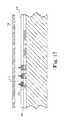
- FIG. 9is a cross-sectional view of an alternate probe assembly in accordance with an embodiment of the present disclosure.
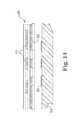
- FIG. 10is a cross-sectional view of a probe assembly with circuitry layers in accordance with an embodiment of the present disclosure.
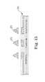
- FIG. 11is a cross-sectional view of a probe assembly with electrical devices in accordance with an embodiment of the present disclosure.
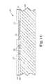
- FIG. 12is a cross-sectional view of a multi-layered probe assembly in accordance with an embodiment of the present disclosure.
- FIG. 13is a cross-sectional view of a probe assembly with coupling features in accordance with an embodiment of the present disclosure.
- FIG. 14is a cross-sectional view of the probe assembly of FIG. 13 with capacitive coupling features instead of probe members in accordance with an embodiment of the present disclosure.
- FIG. 15illustrates a method of reworking a probe assembly in accordance with an embodiment of the present disclosure.
- FIG. 16illustrates an alternate method of making a probe assembly in accordance with an embodiment of the present disclosure.
- FIG. 17illustrates the probe assembly of FIG. 16 with bumps applied in accordance with an embodiment of the present disclosure.
- FIG. 18illustrates an alternate method of making a probe assembly in accordance with an embodiment of the present disclosure.
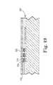
- FIG. 19illustrates application of a second circuitry layer to the probe assembly of FIG. 18 .
- FIG. 20illustrates a probe assembly with bulk metal deposited in recesses to form the vias in accordance with an embodiment of the present disclosure.
- FIG. 21illustrates a probe assembly with recesses filed with conductive particles as the vias in accordance with an embodiment of the present disclosure.
- the present disclosurerelates to a high performance probe assembly for testing wafer-level integrated circuits.
- the present probe assemblycan be used with electrical devices having contact-to-contact spacing (pitch) on the order of less than about 1.0 millimeter (1 ⁇ 10 ⁇ 3 meters), and more preferably a pitch of less than about 0.7 millimeter, and most preferably a pitch of less than about 0.4 millimeter.
- pitchcontact-to-contact spacing
- Such fine pitch probe assembliesare especially useful for probing wafer-level integrated circuits.
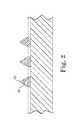
- FIG. 1illustrates a probe assembly 50 that leverages the principle of stud bumping in accordance with an embodiment of the present disclosure.
- Stud bumpingis a derivation of wire bonding, both of which have been used for many years in the semiconductor packaging industry. In recent years, the cost of gold has driven a migration to the use of copper bonding wire in an effort to reduce cost.
- Substrate 56is positioned appropriately within the bond area and stud bumps 54 are bonded to bonding pads 52 on the substrate 56 .
- the wire on the stub bumping machineis broken off at a pre-determined point after the leading end of the wire is bonded to bonding pad 52 .
- the bumps 54are arranged in a pattern that corresponds to the target device to be connected, such as an integrated circuit (“IC”) device.
- the stub bumps 54add metal above the surface of the substrate 56 to facilitate a probe tip or contact point.
- a tamping toolis used to coin bump 54 into a more planar height and consistent shape relative to adjacent bumps.
- the stub bumps 54are connected to a circuit routing in the substrate 56 .
- the substrate 56optionally includes circuitry 58 electrically coupled to the bumps 54 .
- the substrate 56 and/or the circuitry 58are then connected to a test system.
- the present methodpermits the use of copper, which enhances the durability of the present probe assembly 50 because copper is much harder than gold.
- the various probe assemblies of the present disclosurecan be further processed to increase the mechanical robustness as well as provide a low cost interconnect method compared to gold.
- the bumps 54are coined or tamped to create a more uniform and planar peak height 55 with a shape more conductive to probing small targets.
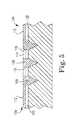
- FIG. 3illustrates an alternate embodiment in which the bumps 54 are coined planar to create a target for another bump to be bonded to increase the overall extension beyond the substrate.
- a thick resist 60can also be applied and the bond sites be extended by copper plating 62 to resemble copper pillars.
- FIGS. 4 through 7illustrate a method for building circuitry 100 in a substrate 102 of a probe assembly 104 that connects the bumps 106 to test equipment in accordance with an embodiment of the present disclosure.
- the bumps 106are located in protective structure 108 .
- the protective structure 108provide a platform for processing the interconnecting circuitry on backside 110 where the substrate 102 .
- the added circuitry and routingcan be provided with a dielectric patterning method that provides an optional means to add function and interconnectivity.
- dielectrics 114are printed or imaged to define the circuitry 100 .
- Conductive traces 112 for the circuitry 100are formed on the substrate 102 that connect to the bumps 106 .
- the conductive traces 112are manufactured to provide the corresponding routing and terminal fan-out to enable connection to the test electronics.
- the conductive traces 112may be deposited or printed on backside 110 of the substrate 102 .
- the conductive traces 112are a metallic powder deposited in recesses created by the dielectric 114 and sintered.
- the conductive traces 112are a flowable, curable conductive material.
- the conductive traces 112can also be created by foil transfer plated to the previous targets or applying a platable target catalyst which is post print plated.
- Various methods for maskless deposition of electronic materialssuch as inkjet printing technology as will be described below, may also be used to deposit the conductive traces 112 on the substrate 102 .
- the platingis optionally applied using printing technology, such as for example inkjet printing technology, aerosol printing technology, or other maskless deposition process.
- the printing processis additive in nature.
- Digital images of the dielectric layers 114 and conductive traces 112are printed directly on the surface 110 , eliminating or reducing many of the lithography, plating, and etching steps used to manufacture conventional probes.
- the resulting probe assembly 104(see FIG. 8 ) provides high frequency capability, and can reduce manufacturing production time and cost by orders of magnitude.
- the dielectric layer 114can optionally be filled or doped with a near endless list of enhancement materials to lower dielectric constant, provide thermal management properties, create rigid, flexible, or compliant regions, and the like.
- the dielectric layers of the present disclosuremay be constructed of any of a number of dielectric materials that are currently used to make sockets, semiconductor packaging, and printed circuit boards. Examples may include UV stabilized tetrafunctional epoxy resin systems referred to as Flame Retardant 4 (FR-4); bismaleimide-triazine thermoset epoxy resins referred to as BT-Epoxy or BT Resin; and liquid crystal polymers (LCPs), which are polyester polymers that are extremely unreactive, inert and resistant to fire. Other suitable plastics include phenolics, polyesters, and Ryton® available from Phillips Petroleum Company.
- one or more of the dielectric materialsare designed to provide electrostatic dissipation or to reduce cross-talk between the traces of the circuit geometry.
- An efficient way to prevent electrostatic discharge (“ESD”)is to construct one of the layers from materials that are not too conductive but that will slowly conduct static charges away. These materials preferably have resistivity values in the range of 10 5 to 10 11 Ohm-meters.
- the resulting conductive traces 112preferably have substantially rectangular cross-sectional shapes.
- the use of additive printing processespermits conductive material, non-conductive material, and semi-conductive material to be simultaneously located on a single layer.
- recesses 116(or trenches) formed on the substrate 102 that permit control of the location, cross section, material content, and aspect ratio of the conductive traces 112 . Maintaining the conductive traces 112 with a cross-section of 1:1 or greater can provide greater signal integrity than traditional subtractive trace forming technologies. For example, traditional methods take a sheet of a given thickness and etch the material between the traces away to have a resultant trace that is usually wider than it is thick. The etching process also removes more material at the top surface of the trace than at the bottom, leaving a trace with a trapezoidal cross-sectional shape, degrading signal integrity in some applications. Using recesses to control the aspect ratio of the conductive traces 64 can result in a more rectangular or square cross-section of the conductive traces, with a corresponding improvement in signal integrity.
- pre-patterned or pre-etched thin conductive foil circuit tracescan be transferred to the recesses 116 .
- a pressure sensitive adhesivecan be used to retain the copper foil circuit traces in the recesses 116 .
- the trapezoidal cross-sections of the pre-formed conductive foil tracesare then post-plated.
- the plating materialfills the open spaces in the recesses 116 , resulting in a substantially rectangular or square cross-sectional shape corresponding to the shape of the recesses 116 .
- a thin conductive foilis pressed into the recesses 116 , and the edges of the recesses 116 act to cut or shear the conductive foil.
- the processpositions a portion of the conductive foil in the recesses 116 , but leaves the negative pattern of the conductive foil not wanted outside and above the recesses 116 for easy removal.
- the foil in the recesses 116is preferably post plated to add material to increase the thickness of the conductive traces 112 and to fill any voids left between the conductive foil and the recesses 116 .
- FIG. 6illustrates a compliant layer 118 deposited on a surface 120 of the dielectric layers 114 and the conductive traces 112 .
- the compliant layer 118is preferably printed onto the surface 120 .
- the compliant layer 118can be printed using inkjet printing technology, aerosol printing technology, or other maskless deposition techniques as previously described.
- the compliant layer 118provides normal force and actuation compliance.
- the compliant layer 118can be bonded to the surface 120 .
- “bond” or “bonding”refers to, for example, adhesive bonding, solvent bonding, ultrasonic welding, thermal bonding, or any other techniques suitable for attaching adjacent layers to a substrate.
- FIG. 7illustrates a protective layer 122 added to a top surface 124 of the compliant layer 118 .
- the protective layer 122can be applied using printing technology or can be a patterned film bonded to the top surface 124 .
- the bumped substrate 102can then be processed with post bump operations to harden or strengthen the bumps 106 since they are copper and remain relatively ductile although much harder than gold.
- Various metalssuch as nickel, nickel boron, palladium cobalt, rhodium, etc. can be plated onto the bumps to increase the wear resistance and reduce contamination during use.
- FIG. 8illustrates the probe assembly 104 of FIG. 7 removed from the fixture 108 .
- Exposed portions 130 of the bumps 106are optionally plated.
- the bumps 106are further processed, such as for example by coining or etching, to facilitate engagement with terminals 132 on a circuit member 134 .
- the present probe assembly 104can be particularly well suited for probing wafer-level integrated circuits, it can be used on a variety of other circuit members, such as for example, packaged integrated circuits, unpackaged integrated circuits, printed circuit boards, flexible circuits, bare-die devices, organic or inorganic substrates, or any other device capable of carrying electrical current.
- a normal force 136can be applied to a top surface 138 of the probe assembly 104 (on the protective layer 122 ) so the distal ends 140 of the bumps 106 electrically couple with the terminals 132 on the circuit member 134 .
- the compliant layer 118can compensate for non-planarity at the interface 142 .
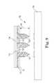
- FIG. 9is a cross-sectional view of an alternate probe assembly 150 with gaps 152 , 154 in dielectric layers 156 , 158 in accordance with an embodiment of the present disclosure.
- the gaps 152 , 154are located substantially adjacent to probe members 160 to provide a degree of compliance.
- the gaps 152 , 154decouple compliance of probe members 160 from the dielectric layers 156 , 158 .
- a height 162 of the probe members 160can be increased to reduce the chance of a bottom surface 164 of the dielectric layer 156 contacting a wafer 166 .
- FIG. 10is a cross-sectional view of an alternate probe assembly 170 with additional functional layers 172 A, 172 B, 172 C (collectively “ 172 ”), in accordance with an embodiment of the present disclosure.
- the functional layerscan be, for example, specialty dielectrics, ground planes, power planes, shielding layers, stiffening layers, capacitive coupling features, circuitry layers, and the like.
- the layers 172can be printed or preformed and selectively bonded or non-bonded to provide contiguous material or releasable layers.
- layers 172 A and 1726are ground planes.
- Layer 172 Cis a compliant layer that operates in either alone or in conjunction with gaps 174 adjacent to the probe members 176 to compensate for non-planarity at the interface 178 with the wafer 180 .
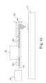
- FIG. 11is a cross-sectional view of a probe assembly 200 with additional electrical devices 202 in accordance with embodiments of the present disclosure.
- the electrical devices 202can be capacitors, transistors, resistors, filters, signal or power altering and enhancing devices, memory devices, an embedded IC, an RF antennae, and the like.
- the electrical devices 202can be located on surface 204 or embedded in one of the layers.
- the probe assembly 200can include an extension 208 , such as for example a flexible circuit member, electrically coupling conductive traces 210 to test station 206 .
- the electrical devices 202can be added as discrete components or printed onto one of the layers.
- the electrical devices 202can be printed using inkjet printing technology, aerosol printing technology, or other maskless deposition techniques, as previously described. Electrical devices that are typically located on the test station 206 can be incorporated into the probe assembly 200 , improving electrical performance.
- the electrical devices 202monitor the testing of the circuit member 212 and communicate feedback to the test station 206 .
- a feedback signal from the electronic devices 202can cause the test station 206 to alter the testing protocol depending on the performance of the circuit member 212 , referred to as adaptive testing.
- the feedback signal from the electronic devices 202can cause the test station 206 to alter the circuit member 212 , such as for example, by altering software resident on the circuit member 212 .
- the electrical devices 202can include passive or active functional elements.
- Passive structurerefers to a structure having a desired electrical, magnetic, or other property, including but not limited to a conductor, resistor, capacitor, inductor, insulator, dielectric, suppressor, filter, varistor, ferromagnet, and the like.
- electrical devices 202include printed LED indicator and display electronics. Geometries can also be printed to provide capacitive coupling. Compliant material can be added between circuit geometry, such as discussed above, so the present electrical interconnect can be plugged into a receptacle or socket, supplementing or replacing the need for compliance within the connector.
- the electrical devices 202are preferably printed during construction of the interconnect assembly 200 .
- the electrical devices 202can be ground planes, power planes, electrical connections to other circuit members, dielectric layers, conductive traces, transistors, capacitors, resistors, RF antennae, shielding, filters, signal or power altering and enhancing devices, memory devices, embedded IC, and the like.
- the electrical devices 202can be formed using printing technology, adding intelligence to the high performance electrical interconnect 200 .
- Features that are typically located on other circuit memberscan be incorporated into the interconnect 200 in accordance with an embodiment of the present disclosure.
- 6,750,473(Amundson et al.), which are incorporated by reference, teach using ink-jet printing to make various electrical devices, such as, resistors, capacitors, diodes, inductors (or elements which may be used in radio applications or magnetic or electric field transmission of power or data), semiconductor logic elements, electro-optical elements, transistor (including, light emitting, light sensing or solar cell elements, field effect transistor, top gate structures), and the like.
- the electrical devices 202can also be created by aerosol printing, such as disclosed in U.S. Pat. No. 7,674,671 (Renn et al.); U.S. Pat. No. 7,658,163 (Renn et al.); U.S. Pat. No. 7,485,345 (Renn et al.); U.S. Pat. No. 7,045,015 (Renn et al.); and U.S. Pat. No. 6,823,124 (Renn et al.), which are hereby incorporated by reference.
- Printing processesare preferably used to fabricate various functional structures, such as conductive paths and electrical devices, without the use of masks or resists.
- Features down to about 10 micronscan be directly written in a wide variety of functional inks, including metals, ceramics, polymers and adhesives, on virtually any substrate—silicon, glass, polymers, metals and ceramics.
- the substratescan be planar and non-planar surfaces.
- the printing processis typically followed by a thermal treatment, such as in a furnace or with a laser, to achieve dense functionalized structures.
- Ink jet printing of electronically active inkscan be done on a large class of substrates, without the requirements of standard vacuum processing or etching.
- the inksmay incorporate mechanical, electrical or other properties, such as, conducting, insulating, resistive, magnetic, semi conductive, light modulating, piezoelectric, spin, optoelectronic, thermoelectric or radio frequency.
- a plurality of ink dropsare dispensed from the print head directly to a substrate or on an intermediate transfer member.
- the transfer membercan be a planar or non-planar structure, such as a drum.
- the surface of the transfer membercan be coated with a non-sticking layer, such as silicone, silicone rubber, or Teflon.
- the ink(also referred to as function inks) can include conductive materials, semi-conductive materials (e.g., p-type and n-type semiconducting materials), metallic material, insulating materials, and/or release materials.
- the ink patterncan be deposited in precise locations on a substrate to create fine lines having a width smaller than 10 microns, with precisely controlled spaces between the lines.
- the ink dropsform an ink pattern corresponding to portions of a transistor, such as a source electrode, a drain electrode, a dielectric layer, a semiconductor layer, or a gate electrode.
- the substratecan be an insulating polymer, such as polyethylene terephthalate (PET), polyester, polyethersulphone (PES), polyimide film (e.g. Kapton, available from DuPont located in Wilmington, Del.; Upilex available from Ube Corporation located in Japan), or polycarbonate.
- PETpolyethylene terephthalate
- PETpolyethylene terephthalate
- PETpolyethersulphone
- polyimide filme.g. Kapton, available from DuPont located in Wilmington, Del.; Upilex available from Ube Corporation located in Japan
- polycarbonatee.g. Kapton, available from DuPont located in Wilmington, Del.; Upilex available from Ube Corporation located in Japan
- the substratecan be made of an insulator such as undoped silicon, glass, or a plastic material.
- the substratecan also be patterned to serve as an electrode.
- the substratecan further be a metal foil insulated from the gate electrode by a non-conducting material.
- the substratecan also be
- Electrodescan be printed with metals, such as aluminum or gold, or conductive polymers, such as polythiophene or polyaniline.
- the electrodesmay also include a printed conductor, such as a polymer film comprising metal particles, such as silver or nickel, a printed conductor comprising a polymer film containing graphite or some other conductive carbon material, or a conductive oxide such as tin oxide or indium tin oxide.
- Dielectric layerscan be printed with a silicon dioxide layer, an insulating polymer, such as polyimide and its derivatives, poly-vinyl phenol, polymethylmethacrylate, polyvinyldenedifluoride, an inorganic oxide, such as metal oxide, an inorganic nitride such as silicon nitride, or an inorganic/organic composite material such as an organic-substituted silicon oxide, or a sol-gel organosilicon glass.
- Dielectric layerscan also include a bicylcobutene derivative (BCB) available from Dow Chemical (Midland, Mich.), spin-on glass, or dispersions of dielectric colloid materials in a binder or solvent.
- BCBbicylcobutene derivative
- Semiconductor layerscan be printed with polymeric semiconductors, such as, polythiophene, poly(3-alkyl)thiophenes, alkyl-substituted oligothiophene, polythienylenevinylene, poly(para-phenylenevinylene) and doped versions of these polymers.
- polymeric semiconductorssuch as, polythiophene, poly(3-alkyl)thiophenes, alkyl-substituted oligothiophene, polythienylenevinylene, poly(para-phenylenevinylene) and doped versions of these polymers.
- An example of suitable oligomeric semiconductoris alpha-hexathienylene. Horowitz, Organic Field-Effect Transistors, Adv. Mater., 10, No. 5, p. 365 (1998) describes the use of unsubstituted and alkyl-substituted oligothiophenes in transistors.
- a field effect transistor made with regioregular poly(3-hexylthiophene) as the semiconductor layeris described in Bao et al., Soluble and Processable Regioregular Poly(3-hexylthiophene) for Thin Film Field-Effect Transistor Applications with High Mobility, Appl. Phys. Lett. 69 (26), p. 4108 (December 1996).
- a field effect transistor made with a-hexathienyleneis described in U.S. Pat. No. 5,659,181, which is incorporated herein by reference.
- a protective layercan optionally be printed onto the electrical devices.
- the protective layercan be an aluminum film, a metal oxide coating, a polymeric film, or a combination thereof.
- Organic semiconductorscan be printed using suitable carbon-based compounds, such as, pentacene, phthalocyanine, benzodithiophene, buckminsterfullerene or other fullerene derivatives, tetracyanonaphthoquinone, and tetrakisimethylanimoethylene.
- suitable carbon-based compoundssuch as, pentacene, phthalocyanine, benzodithiophene, buckminsterfullerene or other fullerene derivatives, tetracyanonaphthoquinone, and tetrakisimethylanimoethylene.
- suitable carbon-based compoundssuch as, pentacene, phthalocyanine, benzodithiophene, buckminsterfullerene or other fullerene derivatives, tetracyanonaphthoquinone, and tetrakisimethylanimoethylene.
- the ink-jet print headpreferably includes a plurality of orifices for dispensing one or more fluids onto a desired media, such as for example, a conducting fluid solution, a semiconducting fluid solution, an insulating fluid solution, and a precursor material to facilitate subsequent deposition.
- a desired mediasuch as for example, a conducting fluid solution, a semiconducting fluid solution, an insulating fluid solution, and a precursor material to facilitate subsequent deposition.
- the precursor materialcan be surface active agents, such as octadecyltrichlorosilane (OTS).
- a separate print headis used for each fluid solution.
- the print head nozzlescan be held at different potentials to aid in atomization and imparting a charge to the droplets, such as disclosed in U.S. Pat. No. 7,148,128 (Jacobson), which is hereby incorporated by reference.
- Alternate print headsare disclosed in U.S. Pat. No. 6,626,526 (Ueki et al.), and U.S. Pat. Publication Nos. 2006/0044357 (Andersen et al.) and 2009/0061089 (King et al.), which are hereby incorporated by reference.
- the print headpreferably uses a pulse-on-demand method, and can employ one of the following methods to dispense the ink drops: piezoelectric, magnetostrictive, electromechanical, electro pneumatic, electrostatic, rapid ink heating, magneto hydrodynamic, or any other technique well known to those skilled in the art.
- the deposited ink patternstypically undergo a curing step or another processing step before subsequent layers are applied.
- printingis intended to include all forms of printing and coating, including: pre-metered coating such as patch die coating, slot or extrusion coating, slide or cascade coating, and curtain coating; roll coating such as knife over roll coating, forward and reverse roll coating; gravure coating; dip coating; spray coating; meniscus coating; spin coating; brush coating; air knife coating; screen printing processes; electrostatic printing processes; thermal printing processes; and other similar techniques.
- pre-metered coatingsuch as patch die coating, slot or extrusion coating, slide or cascade coating, and curtain coating
- roll coatingsuch as knife over roll coating, forward and reverse roll coating
- gravure coatingdip coating
- spray coatingmeniscus coating
- spin coatingspin coating
- brush coatingair knife coating
- screen printing processeselectrostatic printing processes
- thermal printing processesand other similar techniques.
- FIG. 12is a cross-sectional view of a probe assembly 220 with multiple layers 222 in accordance with an embodiment of the present disclosure.
- the probe assembly 220can permit IC manufactures to reduce the pitch 224 of the terminals 226 on the IC devices 228 since the required signal routing to a test station 230 is performed by the probe assembly 220 .
- FIG. 13is a cross-sectional view of a probe assembly 230 with coupling features 232 in accordance with an embodiment of the present disclosure.
- the coupling features 232can be capacitive couplings located between dielectric layers 234 , 236 .
- the coupling features 232can be optical fibers supported by the dielectric layers 234 , 236 .
- Optical quality materialscan optionally be printed directly onto the dielectric layers 234 , 236 .
- the printing processcan also allow for deposition of coatings in-situ that will enhance the optical transmission or reduce loss. The precision of the printing process can resolve misalignment issues when the optical fibers 232 are placed into a connector.
- the coupling features 232can be embedded coaxial or printed micro strip RF circuits with dielectric layers 234 , 236 .
- the dielectric layers 234 , 236can be formed of metal. Any of the structures noted above, as well as the probe members 240 , can be created by printing dielectrics and metallization geometry.
- FIG. 14illustrates the probe assembly 250 of FIG. 13 with probe members 240 (shown in FIG. 13 ) removed.
- Optional different dielectric materials 252can be located where the probe members 250 were located.
- the coupling features 252can capacitively couple with terminals 254 on the wafer 256 due to the very precise planar nature of the printing process.
- FIG. 15illustrates a probe assembly 270 on which damaged probe members are removed and new probe members 272 are re-printed.
- the illustrated embodimentdiscloses triangular shaped probe members 272 , a variety of other non-triangular shapes can be created using printing technology.
- FIG. 16is a side cross-sectional view of a method of making a probe assembly 300 using additive processes in accordance with an embodiment of the present disclosure.
- the processstarts similar to a traditional PCB with a first circuitry layer 302 laminated to a stiffening layer or core 304 , such as glass-reinforced epoxy laminate sheets (e.g., FR4).
- the first circuitry layer 302can be preformed or can be formed using a fine line imaging step is conducted to etch the copper foil as done with many PCB processes.
- One or more dielectric layers 306 , 308are printed or placed to the surface 310 such that the first circuitry layer 302 is at least partially encased and isolated.
- Recesses 312 in the dielectric layer 308 to expose circuitry 302can be formed by printing, embossing, imprinting, chemical etching with a printed mask, or a variety of other techniques.
- the exposed circuitry 302can be stud bumped or ball bonded 314 with a traditional bonding machine used in semiconductor packaging applications.
- copper foil layer 316is applied surface 318 so that the bumps 314 engage with the foil 316 and deforms to create the interconnecting via during the lamination operation.
- the size and shape of the bumps 314can be tailored to the ideal condition for deformation without piercing the foil 316 .
- the foil 316can be pre-etched with the next circuit pattern or can be laminated as a sheet and etched post lamination.
- the dielectric material 308can be left in a tack cure or partial cure state such that a final bond is achieved at final cure. If desired, the bond bumps 314 can be coined planar prior to adding the subsequent foil layer 316 .
- FIGS. 18 and 19illustrate an variation of the probe assembly 300 in which the foil layer 316 includes preformed holes or breaks 320 in accordance with an embodiment of the present disclosure.
- the bumps 314extend into the openings 320 or reside near the openings 320 so plating solution 322 can enter the mating region to plate the via structure 324 together.
- the plating 322is preferably a corrosion resistant metallic material such as nickel, gold, silver, palladium, or multiple layers thereof.
- One benefit of the present structureis the material set can be varied layer by layer or altered on a given layer to create some desired performance enhancement not possible with conventional construction.
- FIG. 20illustrates an alternate probe assembly 350 with solid bulk metal 352 , such as copper or solder spheres, or plated copper, located in recesses 354 in dielectric layer 356 in accordance with an embodiment of the present disclosure.
- the bulk metal 352electrically couples with the lower circuitry layer 358 and the upper circuitry layer 360 with slight deformation or material displacement.
- the bulk metal 352is plated, such as by flowing a plating solution through openings 362 in the upper circuitry 360 . It may be possible to provide sufficient engagement to interconnect reliably without the need for plating since the bulk metal 352 is encased within dielectric 356 and environmentally sealed.
- the circuit layers 358 , 360can be interconnected when the solder 352 is reflowed with the dielectric 356 acting as a natural solder wicking barrier.
- FIG. 21illustrates an alternate probe assembly 370 with reservoirs 372 between circuitry layers 374 , 376 that can be filled with loose conductive particles 378 in accordance with an embodiment of the present disclosure.
- the conductive particles 378can optionally be sintered, coined, tightly compacted, plated, mixed with an adhesive binder, etc. to create via 380 .
- the method of FIG. 21can also be used to create the circuitry itself or supplement the etched foil structures.
- Use of reservoirs containing conductive particlesis disclosed in commonly assigned PCT/US2010/36313 entitled Resilient Conductive Electrical Interconnect, filed May 27, 2010, which is hereby incorporated by reference.
- the probe assembly 370can also be mated with a variety of connection techniques, with the routing to the tester terminated in a Land Pad to simulate a LGA device or Board to Board format as well as terminated in BGA style terminals either of solder or plated copper to facilitate an easily removed and replaced probe assembly or structure where the probe assembly is easily removed from the probe card.
Landscapes
- Engineering & Computer Science (AREA)
- Computer Hardware Design (AREA)
- Microelectronics & Electronic Packaging (AREA)
- General Engineering & Computer Science (AREA)
- Physics & Mathematics (AREA)
- General Physics & Mathematics (AREA)
- Testing Or Measuring Of Semiconductors Or The Like (AREA)
Abstract
Description
- The present application claims the benefit of U.S. Provisional Application No. 61/449,871, entitled Bumped Semiconductor Wafer or Die Level Electrical Interconnect, filed Mar. 7, 2011.
- This application is continuation-in-part of U.S. patent application Ser. No. 13/266,522, titled COMPLIANT WAFER LEVEL PROBE ASSEMBLY, filed Oct. 27, 2011, which is a national stage application under 35 U.S.C. §371 of International Application No. PCT/US2010/036047, titled COMPLIANT WAFER LEVEL PROBE ASSEMBLY, filed May 25, 2010, which claims priority to U.S. Provisional Application No. 61/183,856, filed Jun. 3, 2009, both of which are hereby incorporated by reference in their entireties.
- This application is a continuation-in-part of U.S. patent application Ser. No. 13/266,573, titled COMPLIANT PRINTED CIRCUIT AREA ARRAY SEMICONDUCTOR DEVICE PACKAGE, filed Oct. 27, 2011, which is a national stage application under 35 U.S.C. §371 of International Application No. PCT/US2010/036363, titled COMPLIANT PRINTED CIRCUIT AREA ARRAY SEMICONDUCTOR DEVICE PACKAGE, filed May 27, 2010, which claims priority to U.S. Provisional Application No. 61/183,411, filed Jun. 2, 2009, all of which are hereby incorporated by reference in their entireties.
- This application is a continuation-in-part of U.S. patent application Ser. No. 13/318,203, entitled COMPLIANT PRINTED CIRCUIT SEMICONDUCTOR TESTER INTERFACE, filed Oct. 7, 2011, which is a national stage application under 35 U.S.C. §371 of International Application No. PCT/US2010/040188, titled COMPLIANT PRINTED CIRCUIT SEMICONDUCTOR TESTER INTERFACE, filed Jun. 28, 2010, which claims priority to U.S. Provisional Application No. 61/221,356, filed Jun. 29, 2009, all of which are hereby incorporated by reference in their entireties.
- This application is a continuation-in-part of U.S. patent application Ser. No. 13/319,228, entitled SINGULATED SEMICONDUCTOR DEVICE SEPARABLE ELECTRICAL INTERCONNECT, filed Nov. 7, 2011, which is a national stage application under 35 U.S.C. §371 of International Application No. PCT/US2010/040197, titled SINGULATED SEMICONDUCTOR DEVICE SEPARABLE ELECTRICAL INTERCONNECT, filed Jun. 28, 2010, which claims priority to U.S. Provisional Application No. 61/221,380, filed Jun. 29, 2009, all of which are hereby incorporated by reference in their entireties.
- The present application is a continuation-in-part of International Application No. PCT/US2011/062313, titled HIGH PERFORMANCE SURFACE MOUNT ELECTRICAL INTERCONNECT, filed Nov. 29, 2011, which claims the benefit of U.S. Provisional Application No. 61/418,625, filed Dec. 1, 2010, which are hereby incorporated by reference in their entireties.
- The present disclosure relates to a probe assembly for testing electrical devices, and in particular, to a probe assembly that forms a temporary electrical interconnect between a wafer-level electrical device and a test station.
- During the semiconductor production process, manufacturers typically test integrated circuit (IC) devices while they are still grouped together as built on a silicon wafer. These tests verify various manufacturing parameters as well as chip function when possible. The connection points or terminals that will eventually be connected to the semiconductor package are typically very small and tightly spaced to conserve space on the wafer and allow for more ICs in the given area. Since the terminals are so small and tightly spaced, specialized tool sets are used to connect the IC to test electronics of a test station.
- In basic terms, a precision piece of equipment called a probe station includes a customized precision connection device called a probe card mounted in a manner that allows contact tips of the probe card to be located directly over the terminal pads of the IC device on the silicon wafer. This probe card typically includes contact tips that correspond to the terminals to be contacted and the circuitry on the probe card routes the connection to a test station, which can be a general or special purpose computer.
- When the device is powered, the test station looks for specific results and software determines if the IC passes or fails the test. Some applications allow for multiple devices to be contacted and tested at one time, increasing throughput of the testing process. Traditional probe cards consist of a variety of methods to transition the very small and tightly spaced terminal connections on the wafer to more widely spaced connections of the interface to a test station.
- One probe style is called a cantilever needle, which is essentially a long precise wire that is shaped and positioned such that the contact tip is located where the terminal on the wafer will be during use to test an electrical device. Groups of needles are assembled into the probe card assembly and each needle is adjusted such that the field of tips all contact the desired terminal positions. Needle probes are typically the least expensive, are well established in the industry, and are widely available.
- For mechanical reasons, the needles are relatively long (inches) to provide the required spring properties. Long contact members, however, tend to reduce the electrical performance of the connection by creating a parasitic effect that impacts the signal as it travels through the contact. Resistance in the contacts impacts the self heating effects as current passes through power delivery contacts. Also, the small space between contacts can cause distortion known as cross talk as a nearby contact may influence its neighbor. In most cases, the tests that are run using needle probes are typically basic on-off tests due to the limited signal integrity.
- Another probe style is called a buckling beam or vertical probe. Basically, a series of very fine wires can be precisely located within an assembly that locates and guides each wire such that it can be located directly above the IC terminal to be connected. Buckling beam probes have been used for many years and can be based upon IBM technology that is over 20 years old. These probes are usually more expensive, and are typically used for area array connections. Again, the length of the contact wire to allow the beam to buckle is relatively large, so the signal performance can be impacted.
- Another probe style is based upon a small precisely formed wire called a micro spring that is created on a sophisticated substrate in such a way that the tip of the wire is in position to contact the desired terminal on the wafer. There are also probe types that are made with semiconductor style processes, creating very small mechanisms commonly referred to as micro-electro-mechanical systems (“MEMS”) devices. Micro spring and MEMS-based probes are typically very expensive, and although better electrically than the longer probe styles, they may have electrical limitations.
- Membrane probes are made using a photolithography process to create a very intricate flexible printed circuit member. The precisely shaped probe tips can be routed to the tester electronics through the circuit traces on the flexible printed circuit member. The probe tips are created with a proprietary process where the desired shape can be coined at the desired location into a sacrificial substrate. A series of plating, lithography, sputtering and etching steps are used to create the final circuit.
- Membrane probes typically have the best signal performance, but can be expensive to build. For applications requiring higher frequency testing, membrane probes are currently the only choice available. The manufacturing process is very complicated, with many thin film, plating and lithography steps. The complexity of the process results in yield loss and the capital requirements are fairly large. The manufacturing process limits the physical height of the probe tips, such that they do not extend very far off the membrane. There is a potential for the membrane probe to collect debris and crush it into the wafer, thereby damaging ICS. Also, the contact tips must be extremely planar relative to the wafer since the probe tips typically have little or no compliance to compensate for non-planarity.
- All of these probe types are rather expensive, costing thousands or even hundreds of thousands of dollars, depending on the type and number of contact points required. Wafer manufactures typically test each device at least once, so durability of the probe tips can be critical.
- As processors and electrical systems evolve, increased terminal count, reductions in the terminal pitch (i.e., the distance between the terminals), and signal integrity have been drivers that impact probe tip requirements. As terminal count increases, a certain degree of compliance is required between the contacts on the IC and the probe tips to accommodate the topographic differences and maintain reliable electrical connections. Next generation systems will operate above 5 GHz and beyond and existing probe cards will not achieve acceptable price/performance levels without significant revision.
- The present disclosure relates to a high performance probe assembly for testing wafer-level integrated circuits. A present probe assembly, according to one embodiment, can form a temporary electrical interconnect between an electrical device and a test station.
- The present probe assembly can provide a low cost alternative to other probe products, by utilizing an additive printing process and unique probe member fabrication process. The nature of the process can allow for very high frequency performance, as well as the addition of on-board electrical devices and circuitry planes that are not available with other probe products. The present probe assembly can be superior to membrane probe products in terms of mechanical performance, manufacturing complexity, electrical performance, and cost.
- The production cost for a probe assembly in accordance with the present disclosure can be a fraction of the cost of producing exiting probe cards. The use of additive processes, such as for example, printed electrical features, reduces the capital cost and lead time for building the present probe assemblies. The additive processes can also increase yields over probe systems that rely on conventional lithography tools and masks.
- Internal compliance of the entire assembly and of individual probe members can greatly increase performance of the present probe assemblies. The ability to build multi-layer structures over a relatively large area can permit terminal pitch on the IC devices to be reduced. The addition of circuitry planes and electrical devices in the present probe assembly can provide performance enhancements not available with current probe systems. The ability to add electrical devices, such as transistors and memory, to the present probe assembly can provide the opportunity to incorporate test intelligence, extending the use of legacy test equipment and improving test performance. The present probe assemblies can provide the opportunity to develop adaptive testing and to alter the circuit members during testing.
- The present disclosure is directed to a probe assembly that acts as a temporary interconnect between terminals on an IC device and a test station. The probe assembly includes a plurality of stud bumps arranged on a first surface of a substrate in a configuration corresponding to the terminal on the IC device. The stud bumps include a shape adapted to temporarily couple with the terminals on the IC device. A plurality of conductive traces on the substrate electrically couple the stud bumps with the test station.
- The substrate optionally includes a compliant layer located under the stud bumps. In one embodiment, the substrate is a multi-layered structure. A protective layer is optionally deposited on the conductive traces. In one embodiment, the conductive traces include a substantially rectangular cross-sectional shape.
- The substrate is optionally a multi-layered structure. The substrate optionally includes at least one additional circuitry plane selected from a ground plane, a power plane, an electrical connection to other circuit members, a dielectric layer, and a flexible circuit. A flexible circuit member can electrically couple the conductive traces to the test station.
- In one embodiment, at least one electrical device is printed on the substrate and electrically coupled to one or more of the conductive traces. The electrical devices are selected from the group consisting of a power plane, ground plane, capacitor, resistor, filters, signal or power altering and enhancing device, capacitive coupling feature, memory device, embedded integrated circuit, and RF antennae.
- The present disclosure is also directed to an IC device test station including a housing with an opening adapted to retain the IC device. An IC device is located in the openings and electrically coupled to the stud bumps. The test station is electrically coupled to the conductive traces and evaluates the IC device.
- The present disclosure is also directed to a method of forming a probe assembly to act as a temporary interconnect between terminals on an IC device and a test station. The method includes depositing a plurality of stud bumps on a first surface of a substrate in a configuration corresponding to the terminal on the IC device. The stud bumps include a shape adapted to temporarily couple with the terminals on the IC device. Conductive traces are formed on the substrate that electrically couple the stud bumps with the test station.
- The use of additive printing processes can permit the material set in a given layer of a probe assembly to vary. Traditional PCB and circuit fabrication methods take sheets of material and stack them up, laminate, and/or drill. Additive printing technologies permit a wide variety of materials to be applied on a layer with a registration relative to the features of the previous layer. Selective addition of conductive, non-conductive, or semi-conductive materials at precise locations to create a desired effect has the major advantages in tuning impedance or adding electrical function on a given layer. Tuning performance on a layer by layer basis relative to the previous layer greatly enhances electrical performance.
- The present disclosure is also directed to a method of adaptive testing of circuit members using the probe assembly of the present invention. Electrical devices on the probe assembly can monitor performance of the circuit member being tested and signal the test station to modify the test protocol accordingly. The test station can also be signaled to modify the circuit member.
FIG. 1 is a cross-sectional view of a method of making a high performance probe assembly in accordance with an embodiment of the present disclosure.FIG. 2 illustrates the probe assembly ofFIG. 1 after a coining operation in accordance with an embodiment of the present disclosure.FIG. 3 illustrates an alternate probe assembly in accordance with an embodiment of the present disclosure.FIG. 4 illustrates a method of forming circuitry on a probe assembly in accordance with an embodiment of the present disclosure.FIG. 5 illustrates conductive traces applied to the probe assembly ofFIG. 4 .FIG. 6 illustrates a compliant layer added to the probe assembly ofFIG. 5 .FIG. 7 illustrates a protective layer added to the probe assembly ofFIG. 6 .FIG. 8 is a cross-sectional view of a probe assembly in accordance with an embodiment of the present disclosure.FIG. 9 is a cross-sectional view of an alternate probe assembly in accordance with an embodiment of the present disclosure.FIG. 10 is a cross-sectional view of a probe assembly with circuitry layers in accordance with an embodiment of the present disclosure.FIG. 11 is a cross-sectional view of a probe assembly with electrical devices in accordance with an embodiment of the present disclosure.FIG. 12 is a cross-sectional view of a multi-layered probe assembly in accordance with an embodiment of the present disclosure.FIG. 13 is a cross-sectional view of a probe assembly with coupling features in accordance with an embodiment of the present disclosure.FIG. 14 is a cross-sectional view of the probe assembly ofFIG. 13 with capacitive coupling features instead of probe members in accordance with an embodiment of the present disclosure.FIG. 15 illustrates a method of reworking a probe assembly in accordance with an embodiment of the present disclosure.FIG. 16 illustrates an alternate method of making a probe assembly in accordance with an embodiment of the present disclosure.FIG. 17 illustrates the probe assembly ofFIG. 16 with bumps applied in accordance with an embodiment of the present disclosure.FIG. 18 illustrates an alternate method of making a probe assembly in accordance with an embodiment of the present disclosure.FIG. 19 illustrates application of a second circuitry layer to the probe assembly ofFIG. 18 .FIG. 20 illustrates a probe assembly with bulk metal deposited in recesses to form the vias in accordance with an embodiment of the present disclosure.FIG. 21 illustrates a probe assembly with recesses filed with conductive particles as the vias in accordance with an embodiment of the present disclosure.- The present disclosure relates to a high performance probe assembly for testing wafer-level integrated circuits. The present probe assembly can be used with electrical devices having contact-to-contact spacing (pitch) on the order of less than about 1.0 millimeter (1×10⁻³meters), and more preferably a pitch of less than about 0.7 millimeter, and most preferably a pitch of less than about 0.4 millimeter. Such fine pitch probe assemblies are especially useful for probing wafer-level integrated circuits.
FIG. 1 illustrates aprobe assembly 50 that leverages the principle of stud bumping in accordance with an embodiment of the present disclosure. Stud bumping is a derivation of wire bonding, both of which have been used for many years in the semiconductor packaging industry. In recent years, the cost of gold has driven a migration to the use of copper bonding wire in an effort to reduce cost.Substrate 56 is positioned appropriately within the bond area and stud bumps54 are bonded tobonding pads 52 on thesubstrate 56. In operation, the wire on the stub bumping machine is broken off at a pre-determined point after the leading end of the wire is bonded tobonding pad 52. Thebumps 54 are arranged in a pattern that corresponds to the target device to be connected, such as an integrated circuit (“IC”) device. The stub bumps54 add metal above the surface of thesubstrate 56 to facilitate a probe tip or contact point. In some cases, a tamping tool is used to coinbump 54 into a more planar height and consistent shape relative to adjacent bumps.- The stub bumps54 are connected to a circuit routing in the
substrate 56. Thesubstrate 56 optionally includescircuitry 58 electrically coupled to thebumps 54. Thesubstrate 56 and/or thecircuitry 58 are then connected to a test system. - The present method permits the use of copper, which enhances the durability of the
present probe assembly 50 because copper is much harder than gold. As will be discussed herein, the various probe assemblies of the present disclosure can be further processed to increase the mechanical robustness as well as provide a low cost interconnect method compared to gold. - As illustrated in
FIG. 2 , thebumps 54 are coined or tamped to create a more uniform andplanar peak height 55 with a shape more conductive to probing small targets. FIG. 3 illustrates an alternate embodiment in which thebumps 54 are coined planar to create a target for another bump to be bonded to increase the overall extension beyond the substrate. A thick resist60 can also be applied and the bond sites be extended by copper plating62 to resemble copper pillars.FIGS. 4 through 7 illustrate a method for buildingcircuitry 100 in asubstrate 102 of aprobe assembly 104 that connects thebumps 106 to test equipment in accordance with an embodiment of the present disclosure. In the illustrated embodiment, thebumps 106 are located inprotective structure 108. Theprotective structure 108 provide a platform for processing the interconnecting circuitry onbackside 110 where thesubstrate 102. In this embodiment, the added circuitry and routing can be provided with a dielectric patterning method that provides an optional means to add function and interconnectivity.- As illustrated in
FIG. 5 ,dielectrics 114 are printed or imaged to define thecircuitry 100. Conductive traces112 for thecircuitry 100 are formed on thesubstrate 102 that connect to thebumps 106. The conductive traces112 are manufactured to provide the corresponding routing and terminal fan-out to enable connection to the test electronics. - The conductive traces112 may be deposited or printed on
backside 110 of thesubstrate 102. In one embodiment, theconductive traces 112 are a metallic powder deposited in recesses created by the dielectric114 and sintered. In another embodiment, theconductive traces 112 are a flowable, curable conductive material. The conductive traces112 can also be created by foil transfer plated to the previous targets or applying a platable target catalyst which is post print plated. Various methods for maskless deposition of electronic materials, such as inkjet printing technology as will be described below, may also be used to deposit the conductive traces112 on thesubstrate 102. - The plating is optionally applied using printing technology, such as for example inkjet printing technology, aerosol printing technology, or other maskless deposition process. The printing process is additive in nature. Digital images of the
dielectric layers 114 andconductive traces 112 are printed directly on thesurface 110, eliminating or reducing many of the lithography, plating, and etching steps used to manufacture conventional probes. The resulting probe assembly104 (seeFIG. 8 ) provides high frequency capability, and can reduce manufacturing production time and cost by orders of magnitude. Thedielectric layer 114 can optionally be filled or doped with a near endless list of enhancement materials to lower dielectric constant, provide thermal management properties, create rigid, flexible, or compliant regions, and the like. - The dielectric layers of the present disclosure may be constructed of any of a number of dielectric materials that are currently used to make sockets, semiconductor packaging, and printed circuit boards. Examples may include UV stabilized tetrafunctional epoxy resin systems referred to as Flame Retardant 4 (FR-4); bismaleimide-triazine thermoset epoxy resins referred to as BT-Epoxy or BT Resin; and liquid crystal polymers (LCPs), which are polyester polymers that are extremely unreactive, inert and resistant to fire. Other suitable plastics include phenolics, polyesters, and Ryton® available from Phillips Petroleum Company.
- In one embodiment, one or more of the dielectric materials are designed to provide electrostatic dissipation or to reduce cross-talk between the traces of the circuit geometry. An efficient way to prevent electrostatic discharge (“ESD”) is to construct one of the layers from materials that are not too conductive but that will slowly conduct static charges away. These materials preferably have resistivity values in the range of 105to 1011Ohm-meters.
- The use of additive printing processes can permit a wide variety of materials to be applied on a layer with a registration relative to the features of the previous layer. Selective addition of conductive, non-conductive, or semi-conductive materials at precise locations to create a desired effect can offer advantages in tuning impedance or adding electrical function on a given layer. Tuning performance on a layer by layer basis relative to the previous layer can greatly enhance electrical performance.
- The resulting
conductive traces 112 preferably have substantially rectangular cross-sectional shapes. The use of additive printing processes permits conductive material, non-conductive material, and semi-conductive material to be simultaneously located on a single layer. - In one embodiment, recesses116 (or trenches) formed on the
substrate 102 that permit control of the location, cross section, material content, and aspect ratio of the conductive traces112. Maintaining the conductive traces112 with a cross-section of 1:1 or greater can provide greater signal integrity than traditional subtractive trace forming technologies. For example, traditional methods take a sheet of a given thickness and etch the material between the traces away to have a resultant trace that is usually wider than it is thick. The etching process also removes more material at the top surface of the trace than at the bottom, leaving a trace with a trapezoidal cross-sectional shape, degrading signal integrity in some applications. Using recesses to control the aspect ratio of the conductive traces64 can result in a more rectangular or square cross-section of the conductive traces, with a corresponding improvement in signal integrity. - In another embodiment, pre-patterned or pre-etched thin conductive foil circuit traces can be transferred to the
recesses 116. For example, a pressure sensitive adhesive can be used to retain the copper foil circuit traces in therecesses 116. The trapezoidal cross-sections of the pre-formed conductive foil traces are then post-plated. The plating material fills the open spaces in therecesses 116, resulting in a substantially rectangular or square cross-sectional shape corresponding to the shape of therecesses 116. - In another embodiment, a thin conductive foil is pressed into the
recesses 116, and the edges of therecesses 116 act to cut or shear the conductive foil. The process positions a portion of the conductive foil in therecesses 116, but leaves the negative pattern of the conductive foil not wanted outside and above therecesses 116 for easy removal. Again, the foil in therecesses 116 is preferably post plated to add material to increase the thickness of theconductive traces 112 and to fill any voids left between the conductive foil and therecesses 116. FIG. 6 illustrates acompliant layer 118 deposited on asurface 120 of thedielectric layers 114 and the conductive traces112. Thecompliant layer 118 is preferably printed onto thesurface 120. Thecompliant layer 118 can be printed using inkjet printing technology, aerosol printing technology, or other maskless deposition techniques as previously described. Thecompliant layer 118 provides normal force and actuation compliance. In another embodiment, thecompliant layer 118 can be bonded to thesurface 120. As used herein, “bond” or “bonding” refers to, for example, adhesive bonding, solvent bonding, ultrasonic welding, thermal bonding, or any other techniques suitable for attaching adjacent layers to a substrate.FIG. 7 illustrates aprotective layer 122 added to atop surface 124 of thecompliant layer 118. Theprotective layer 122 can be applied using printing technology or can be a patterned film bonded to thetop surface 124.- In one embodiment, the bumped
substrate 102 can then be processed with post bump operations to harden or strengthen thebumps 106 since they are copper and remain relatively ductile although much harder than gold. Various metals such as nickel, nickel boron, palladium cobalt, rhodium, etc. can be plated onto the bumps to increase the wear resistance and reduce contamination during use. FIG. 8 illustrates theprobe assembly 104 ofFIG. 7 removed from thefixture 108.Exposed portions 130 of thebumps 106 are optionally plated. In another embodiment, thebumps 106 are further processed, such as for example by coining or etching, to facilitate engagement withterminals 132 on acircuit member 134. Although thepresent probe assembly 104 can be particularly well suited for probing wafer-level integrated circuits, it can be used on a variety of other circuit members, such as for example, packaged integrated circuits, unpackaged integrated circuits, printed circuit boards, flexible circuits, bare-die devices, organic or inorganic substrates, or any other device capable of carrying electrical current.- In operation, a
normal force 136 can be applied to atop surface 138 of the probe assembly104 (on the protective layer122) so the distal ends140 of thebumps 106 electrically couple with theterminals 132 on thecircuit member 134. Thecompliant layer 118 can compensate for non-planarity at theinterface 142. FIG. 9 is a cross-sectional view of analternate probe assembly 150 withgaps dielectric layers gaps members 160 to provide a degree of compliance. Thegaps probe members 160 from thedielectric layers height 162 of theprobe members 160 can be increased to reduce the chance of abottom surface 164 of thedielectric layer 156 contacting awafer 166.FIG. 10 is a cross-sectional view of analternate probe assembly 170 with additionalfunctional layers - In the illustrated embodiment, layers172A and1726 are ground planes.
Layer 172C is a compliant layer that operates in either alone or in conjunction withgaps 174 adjacent to theprobe members 176 to compensate for non-planarity at theinterface 178 with thewafer 180. FIG. 11 is a cross-sectional view of aprobe assembly 200 with additionalelectrical devices 202 in accordance with embodiments of the present disclosure. Theelectrical devices 202 can be capacitors, transistors, resistors, filters, signal or power altering and enhancing devices, memory devices, an embedded IC, an RF antennae, and the like. Theelectrical devices 202 can be located onsurface 204 or embedded in one of the layers. Theprobe assembly 200 can include anextension 208, such as for example a flexible circuit member, electrically couplingconductive traces 210 to teststation 206.- The
electrical devices 202 can be added as discrete components or printed onto one of the layers. Theelectrical devices 202 can be printed using inkjet printing technology, aerosol printing technology, or other maskless deposition techniques, as previously described. Electrical devices that are typically located on thetest station 206 can be incorporated into theprobe assembly 200, improving electrical performance. - In one embodiment, the
electrical devices 202 monitor the testing of thecircuit member 212 and communicate feedback to thetest station 206. In one embodiment, a feedback signal from theelectronic devices 202 can cause thetest station 206 to alter the testing protocol depending on the performance of thecircuit member 212, referred to as adaptive testing. In one embodiment, the feedback signal from theelectronic devices 202 can cause thetest station 206 to alter thecircuit member 212, such as for example, by altering software resident on thecircuit member 212. Theelectrical devices 202 can include passive or active functional elements. Passive structure refers to a structure having a desired electrical, magnetic, or other property, including but not limited to a conductor, resistor, capacitor, inductor, insulator, dielectric, suppressor, filter, varistor, ferromagnet, and the like. In the illustrated embodiment,electrical devices 202 include printed LED indicator and display electronics. Geometries can also be printed to provide capacitive coupling. Compliant material can be added between circuit geometry, such as discussed above, so the present electrical interconnect can be plugged into a receptacle or socket, supplementing or replacing the need for compliance within the connector. - The
electrical devices 202 are preferably printed during construction of theinterconnect assembly 200. Theelectrical devices 202 can be ground planes, power planes, electrical connections to other circuit members, dielectric layers, conductive traces, transistors, capacitors, resistors, RF antennae, shielding, filters, signal or power altering and enhancing devices, memory devices, embedded IC, and the like. For example, theelectrical devices 202 can be formed using printing technology, adding intelligence to the high performanceelectrical interconnect 200. Features that are typically located on other circuit members can be incorporated into theinterconnect 200 in accordance with an embodiment of the present disclosure. - The availability of printable silicon inks provides the ability to print
electrical devices 202, such as disclosed in U.S. Pat. No. 7,485,345 (Renn et al.); U.S. Pat. No. 7,382,363 (Albert et al.); U.S. Pat. No. 7,148,128 (Jacobson); U.S. Pat. No. 6,967,640 (Albert et al.); U.S. Pat. No. 6,825,829 (Albert et al.); U.S. Pat. No. 6,750,473 (Amundson et al.); U.S. Pat. No. 6,652,075 (Jacobson); U.S. Pat. No. 6,639,578 (Comiskey et al.); U.S. Pat. No. 6,545,291 (Amundson et al.); U.S. Pat. No. 6,521,489 (Duthaler et al.); U.S. Pat. No. 6,459,418 (Comiskey et al.); U.S. Pat. No. 6,422,687 (Jacobson); U.S. Pat. No. 6,413,790 (Duthaler et al.); U.S. Pat. No. 6,312,971 (Amundson et al.); U.S. Pat. No. 6,252,564 (Albert et al.); U.S. Pat. No. 6,177,921 (Comiskey et al.); U.S. Pat. No. 6,120,588 (Jacobson); U.S. Pat. No. 6,118,426 (Albert et al.); and U.S. Pat. Publication No. 2008/0008822 (Kowalski et al.), which are hereby incorporated by reference. In particular, U.S. Pat. No. 6,506,438 (Duthaler et al.) and U.S. Pat. No. 6,750,473 (Amundson et al.), which are incorporated by reference, teach using ink-jet printing to make various electrical devices, such as, resistors, capacitors, diodes, inductors (or elements which may be used in radio applications or magnetic or electric field transmission of power or data), semiconductor logic elements, electro-optical elements, transistor (including, light emitting, light sensing or solar cell elements, field effect transistor, top gate structures), and the like. - The
electrical devices 202 can also be created by aerosol printing, such as disclosed in U.S. Pat. No. 7,674,671 (Renn et al.); U.S. Pat. No. 7,658,163 (Renn et al.); U.S. Pat. No. 7,485,345 (Renn et al.); U.S. Pat. No. 7,045,015 (Renn et al.); and U.S. Pat. No. 6,823,124 (Renn et al.), which are hereby incorporated by reference. - Printing processes are preferably used to fabricate various functional structures, such as conductive paths and electrical devices, without the use of masks or resists. Features down to about 10 microns can be directly written in a wide variety of functional inks, including metals, ceramics, polymers and adhesives, on virtually any substrate—silicon, glass, polymers, metals and ceramics. The substrates can be planar and non-planar surfaces. The printing process is typically followed by a thermal treatment, such as in a furnace or with a laser, to achieve dense functionalized structures.
- Ink jet printing of electronically active inks can be done on a large class of substrates, without the requirements of standard vacuum processing or etching. The inks may incorporate mechanical, electrical or other properties, such as, conducting, insulating, resistive, magnetic, semi conductive, light modulating, piezoelectric, spin, optoelectronic, thermoelectric or radio frequency.
- A plurality of ink drops are dispensed from the print head directly to a substrate or on an intermediate transfer member. The transfer member can be a planar or non-planar structure, such as a drum. The surface of the transfer member can be coated with a non-sticking layer, such as silicone, silicone rubber, or Teflon.
- The ink (also referred to as function inks) can include conductive materials, semi-conductive materials (e.g., p-type and n-type semiconducting materials), metallic material, insulating materials, and/or release materials. The ink pattern can be deposited in precise locations on a substrate to create fine lines having a width smaller than 10 microns, with precisely controlled spaces between the lines. For example, the ink drops form an ink pattern corresponding to portions of a transistor, such as a source electrode, a drain electrode, a dielectric layer, a semiconductor layer, or a gate electrode.
- The substrate can be an insulating polymer, such as polyethylene terephthalate (PET), polyester, polyethersulphone (PES), polyimide film (e.g. Kapton, available from DuPont located in Wilmington, Del.; Upilex available from Ube Corporation located in Japan), or polycarbonate. Alternatively, the substrate can be made of an insulator such as undoped silicon, glass, or a plastic material. The substrate can also be patterned to serve as an electrode. The substrate can further be a metal foil insulated from the gate electrode by a non-conducting material. The substrate can also be a woven material or paper, planarized or otherwise modified on at least one surface by a polymeric or other coating to accept the other structures.
- Electrodes can be printed with metals, such as aluminum or gold, or conductive polymers, such as polythiophene or polyaniline. The electrodes may also include a printed conductor, such as a polymer film comprising metal particles, such as silver or nickel, a printed conductor comprising a polymer film containing graphite or some other conductive carbon material, or a conductive oxide such as tin oxide or indium tin oxide.
- Dielectric layers can be printed with a silicon dioxide layer, an insulating polymer, such as polyimide and its derivatives, poly-vinyl phenol, polymethylmethacrylate, polyvinyldenedifluoride, an inorganic oxide, such as metal oxide, an inorganic nitride such as silicon nitride, or an inorganic/organic composite material such as an organic-substituted silicon oxide, or a sol-gel organosilicon glass. Dielectric layers can also include a bicylcobutene derivative (BCB) available from Dow Chemical (Midland, Mich.), spin-on glass, or dispersions of dielectric colloid materials in a binder or solvent.
- Semiconductor layers can be printed with polymeric semiconductors, such as, polythiophene, poly(3-alkyl)thiophenes, alkyl-substituted oligothiophene, polythienylenevinylene, poly(para-phenylenevinylene) and doped versions of these polymers. An example of suitable oligomeric semiconductor is alpha-hexathienylene. Horowitz, Organic Field-Effect Transistors, Adv. Mater., 10, No. 5, p. 365 (1998) describes the use of unsubstituted and alkyl-substituted oligothiophenes in transistors. A field effect transistor made with regioregular poly(3-hexylthiophene) as the semiconductor layer is described in Bao et al., Soluble and Processable Regioregular Poly(3-hexylthiophene) for Thin Film Field-Effect Transistor Applications with High Mobility, Appl. Phys. Lett. 69 (26), p. 4108 (December 1996). A field effect transistor made with a-hexathienylene is described in U.S. Pat. No. 5,659,181, which is incorporated herein by reference.
- A protective layer can optionally be printed onto the electrical devices. The protective layer can be an aluminum film, a metal oxide coating, a polymeric film, or a combination thereof.
- Organic semiconductors can be printed using suitable carbon-based compounds, such as, pentacene, phthalocyanine, benzodithiophene, buckminsterfullerene or other fullerene derivatives, tetracyanonaphthoquinone, and tetrakisimethylanimoethylene. The materials provided above for forming the substrate, the dielectric layer, the electrodes, or the semiconductor layer are exemplary only. Other suitable materials known to those skilled in the art having properties similar to those described above can be used in accordance with the present disclosure.
- The ink-jet print head preferably includes a plurality of orifices for dispensing one or more fluids onto a desired media, such as for example, a conducting fluid solution, a semiconducting fluid solution, an insulating fluid solution, and a precursor material to facilitate subsequent deposition. The precursor material can be surface active agents, such as octadecyltrichlorosilane (OTS).
- Alternatively, a separate print head is used for each fluid solution. The print head nozzles can be held at different potentials to aid in atomization and imparting a charge to the droplets, such as disclosed in U.S. Pat. No. 7,148,128 (Jacobson), which is hereby incorporated by reference. Alternate print heads are disclosed in U.S. Pat. No. 6,626,526 (Ueki et al.), and U.S. Pat. Publication Nos. 2006/0044357 (Andersen et al.) and 2009/0061089 (King et al.), which are hereby incorporated by reference.
- The print head preferably uses a pulse-on-demand method, and can employ one of the following methods to dispense the ink drops: piezoelectric, magnetostrictive, electromechanical, electro pneumatic, electrostatic, rapid ink heating, magneto hydrodynamic, or any other technique well known to those skilled in the art. The deposited ink patterns typically undergo a curing step or another processing step before subsequent layers are applied.
- While ink jet printing is preferred, the term “printing” is intended to include all forms of printing and coating, including: pre-metered coating such as patch die coating, slot or extrusion coating, slide or cascade coating, and curtain coating; roll coating such as knife over roll coating, forward and reverse roll coating; gravure coating; dip coating; spray coating; meniscus coating; spin coating; brush coating; air knife coating; screen printing processes; electrostatic printing processes; thermal printing processes; and other similar techniques.
FIG. 12 is a cross-sectional view of aprobe assembly 220 withmultiple layers 222 in accordance with an embodiment of the present disclosure. Theprobe assembly 220 can permit IC manufactures to reduce thepitch 224 of theterminals 226 on theIC devices 228 since the required signal routing to atest station 230 is performed by theprobe assembly 220.FIG. 13 is a cross-sectional view of aprobe assembly 230 with coupling features232 in accordance with an embodiment of the present disclosure. In one embodiment, the coupling features232 can be capacitive couplings located betweendielectric layers dielectric layers dielectric layers optical fibers 232 are placed into a connector. In another embodiment, the coupling features232 can be embedded coaxial or printed micro strip RF circuits withdielectric layers dielectric layers probe members 240, can be created by printing dielectrics and metallization geometry.FIG. 14 illustrates theprobe assembly 250 ofFIG. 13 with probe members240 (shown inFIG. 13 ) removed. Optional differentdielectric materials 252 can be located where theprobe members 250 were located. The coupling features252 can capacitively couple withterminals 254 on thewafer 256 due to the very precise planar nature of the printing process.FIG. 15 illustrates aprobe assembly 270 on which damaged probe members are removed andnew probe members 272 are re-printed. Although the illustrated embodiment discloses triangular shapedprobe members 272, a variety of other non-triangular shapes can be created using printing technology.FIG. 16 is a side cross-sectional view of a method of making aprobe assembly 300 using additive processes in accordance with an embodiment of the present disclosure. The process starts similar to a traditional PCB with afirst circuitry layer 302 laminated to a stiffening layer orcore 304, such as glass-reinforced epoxy laminate sheets (e.g., FR4). Thefirst circuitry layer 302 can be preformed or can be formed using a fine line imaging step is conducted to etch the copper foil as done with many PCB processes. One or moredielectric layers surface 310 such that thefirst circuitry layer 302 is at least partially encased and isolated. In some embodiments, it may be desirable to use a preformed dielectric film to leave air dielectric gaps between traces.Recesses 312 in thedielectric layer 308 to exposecircuitry 302 can be formed by printing, embossing, imprinting, chemical etching with a printed mask, or a variety of other techniques.- As illustrated in
FIG. 17 , the exposedcircuitry 302 can be stud bumped or ball bonded314 with a traditional bonding machine used in semiconductor packaging applications. In the embodiment below,copper foil layer 316 is appliedsurface 318 so that thebumps 314 engage with thefoil 316 and deforms to create the interconnecting via during the lamination operation. The size and shape of thebumps 314 can be tailored to the ideal condition for deformation without piercing thefoil 316. Thefoil 316 can be pre-etched with the next circuit pattern or can be laminated as a sheet and etched post lamination. In addition, thedielectric material 308 can be left in a tack cure or partial cure state such that a final bond is achieved at final cure. If desired, the bond bumps314 can be coined planar prior to adding thesubsequent foil layer 316. FIGS. 18 and 19 illustrate an variation of theprobe assembly 300 in which thefoil layer 316 includes preformed holes or breaks320 in accordance with an embodiment of the present disclosure. Thebumps 314 extend into theopenings 320 or reside near theopenings 320 so platingsolution 322 can enter the mating region to plate the via structure324 together. Theplating 322 is preferably a corrosion resistant metallic material such as nickel, gold, silver, palladium, or multiple layers thereof. One benefit of the present structure is the material set can be varied layer by layer or altered on a given layer to create some desired performance enhancement not possible with conventional construction.FIG. 20 illustrates analternate probe assembly 350 withsolid bulk metal 352, such as copper or solder spheres, or plated copper, located inrecesses 354 indielectric layer 356 in accordance with an embodiment of the present disclosure. Thebulk metal 352 electrically couples with thelower circuitry layer 358 and theupper circuitry layer 360 with slight deformation or material displacement. In one embodiment, thebulk metal 352 is plated, such as by flowing a plating solution throughopenings 362 in theupper circuitry 360. It may be possible to provide sufficient engagement to interconnect reliably without the need for plating since thebulk metal 352 is encased withindielectric 356 and environmentally sealed. In the event thebulk metal 352 is solder, the circuit layers358,360 can be interconnected when thesolder 352 is reflowed with the dielectric356 acting as a natural solder wicking barrier.FIG. 21 illustrates analternate probe assembly 370 withreservoirs 372 betweencircuitry layers conductive particles 378 in accordance with an embodiment of the present disclosure. Theconductive particles 378 can optionally be sintered, coined, tightly compacted, plated, mixed with an adhesive binder, etc. to create via380. The method ofFIG. 21 can also be used to create the circuitry itself or supplement the etched foil structures. Use of reservoirs containing conductive particles is disclosed in commonly assigned PCT/US2010/36313 entitled Resilient Conductive Electrical Interconnect, filed May 27, 2010, which is hereby incorporated by reference.- The
probe assembly 370 can also be mated with a variety of connection techniques, with the routing to the tester terminated in a Land Pad to simulate a LGA device or Board to Board format as well as terminated in BGA style terminals either of solder or plated copper to facilitate an easily removed and replaced probe assembly or structure where the probe assembly is easily removed from the probe card. - Where a range of values is provided, it is understood that each intervening value, to the tenth of the unit of the lower limit unless the context clearly dictates otherwise, between the upper and lower limit of that range and any other stated or intervening value in that stated range is encompassed within the embodiments of the present invention. The upper and lower limits of these smaller ranges which may independently be included in the smaller ranges is also encompassed within the embodiments of the invention, subject to any specifically excluded limit in the stated range. Where the stated range includes one or both of the limits, ranges excluding either both of those included limits are also included in the embodiments of the invention.
- Unless defined otherwise, all technical and scientific terms used herein have the same meaning as commonly understood by one of ordinary skill in the art to which the embodiments of the invention belong. Although any methods and materials similar or equivalent to those described herein can also be used in the practice or testing of the embodiments of the present invention, the preferred methods and materials are now describe. All patents and publications mentioned herein, including those cited in the Background of the application, are hereby incorporated by reference to disclose and described the methods and/or materials in connection with which the publications are cited.
- The publications discussed herein are provided solely for their disclosure prior to the filing date of the present application. Nothing herein is to be construed as an admission that the embodiments of the present invention are not entitled to antedate such publication by virtue of prior invention. Further, the dates of publication provided may be different from the actual publication dates which may need to be independently confirmed.
- Other embodiments of the invention are possible. Although the description above contains much specificity, these should not be construed as limiting the scope of the invention, but as merely providing illustrations of some of the presently preferred embodiments of this invention. It is also contemplated that various combinations or sub-combinations of the specific features and aspects of the embodiments may be made and still fall within the scope of the invention. It should be understood that various features and aspects of the disclosed embodiments can be combined with or substituted for one another in order to form varying modes of the disclosed embodiments of the present invention. Thus, it is intended that the scope of at least some of the present invention herein disclosed should not be limited by the particular disclosed embodiments described above.
- Thus, the scope of this invention should be determined by the appended claims and their legal equivalents. Therefore, it will be appreciated that the scope of the present invention fully encompasses other embodiments which may become obvious to those skilled in the art, and that the scope of the present invention is accordingly to be limited by nothing other than the appended claims, in which reference to an element in the singular is not intended to mean “one and only one” unless explicitly so stated, but rather “one or more.” All structural, chemical, and functional equivalents to the elements of the above-described preferred embodiment that are known to those of ordinary skill in the art are expressly incorporated herein by reference and are intended to be encompassed by the present claims. Moreover, it is not necessary for a device or method to address each and every problem sought to be solved by the present invention, for it to be encompassed by the present claims. Furthermore, no element, component, or method step in the present disclosure is intended to be dedicated to the public regardless of whether the element, component, or method step is explicitly recited in the claims.
Claims (19)
Priority Applications (1)
| Application Number | Priority Date | Filing Date | Title |
|---|---|---|---|
| US13/413,032US8988093B2 (en) | 2009-06-02 | 2012-03-06 | Bumped semiconductor wafer or die level electrical interconnect |
Applications Claiming Priority (14)
| Application Number | Priority Date | Filing Date | Title |
|---|---|---|---|
| US18341109P | 2009-06-02 | 2009-06-02 | |
| US18385609P | 2009-06-03 | 2009-06-03 | |
| US22138009P | 2009-06-29 | 2009-06-29 | |
| PCT/US2010/036047WO2010141264A1 (en) | 2009-06-03 | 2010-05-25 | Compliant wafer level probe assembly |
| PCT/US2010/036363WO2010141311A1 (en) | 2009-06-02 | 2010-05-27 | Compliant printed circuit area array semiconductor device package |
| PCT/US2010/040197WO2011002712A1 (en) | 2009-06-29 | 2010-06-28 | Singulated semiconductor device separable electrical interconnect |
| US41862510P | 2010-12-01 | 2010-12-01 | |
| US201161449871P | 2011-03-07 | 2011-03-07 | |
| US201113266573A | 2011-10-27 | 2011-10-27 | |
| US201113266522A | 2011-10-27 | 2011-10-27 | |
| US201113319228A | 2011-11-07 | 2011-11-07 | |
| PCT/US2011/062313WO2012074963A1 (en) | 2010-12-01 | 2011-11-29 | High performance surface mount electrical interconnect |
| US201213318203A | 2012-02-14 | 2012-02-14 | |
| US13/413,032US8988093B2 (en) | 2009-06-02 | 2012-03-06 | Bumped semiconductor wafer or die level electrical interconnect |
Related Parent Applications (11)
| Application Number | Title | Priority Date | Filing Date |
|---|---|---|---|
| US13/266,522Continuation-In-PartUS8803539B2 (en) | 2009-06-03 | 2010-05-25 | Compliant wafer level probe assembly |
| PCT/US2010/036047Continuation-In-PartWO2010141264A1 (en) | 2009-06-02 | 2010-05-25 | Compliant wafer level probe assembly |
| PCT/US2010/036363Continuation-In-PartWO2010141311A1 (en) | 2009-06-02 | 2010-05-27 | Compliant printed circuit area array semiconductor device package |
| US13/266,573Continuation-In-PartUS9054097B2 (en) | 2009-06-02 | 2010-05-27 | Compliant printed circuit area array semiconductor device package |
| US13/319,203Continuation-In-PartUS8981809B2 (en) | 2009-06-29 | 2010-06-28 | Compliant printed circuit semiconductor tester interface |
| PCT/US2010/040188Continuation-In-PartWO2011002709A1 (en) | 2009-06-02 | 2010-06-28 | Compliant printed circuit semiconductor tester interface |
| US13/319,228Continuation-In-PartUS8984748B2 (en) | 2009-06-29 | 2010-06-28 | Singulated semiconductor device separable electrical interconnect |
| PCT/US2010/040197Continuation-In-PartWO2011002712A1 (en) | 2009-06-02 | 2010-06-28 | Singulated semiconductor device separable electrical interconnect |
| US201113266522AContinuation-In-Part | 2009-06-02 | 2011-10-27 | |
| PCT/US2011/062313Continuation-In-PartWO2012074963A1 (en) | 2009-06-02 | 2011-11-29 | High performance surface mount electrical interconnect |
| US13/413,032Continuation-In-PartUS8988093B2 (en) | 2009-06-02 | 2012-03-06 | Bumped semiconductor wafer or die level electrical interconnect |
Related Child Applications (1)
| Application Number | Title | Priority Date | Filing Date |
|---|---|---|---|
| US13/413,032Continuation-In-PartUS8988093B2 (en) | 2009-06-02 | 2012-03-06 | Bumped semiconductor wafer or die level electrical interconnect |
Publications (2)
| Publication Number | Publication Date |
|---|---|
| US20120182035A1true US20120182035A1 (en) | 2012-07-19 |
| US8988093B2 US8988093B2 (en) | 2015-03-24 |
Family
ID=46490310
Family Applications (1)
| Application Number | Title | Priority Date | Filing Date |
|---|---|---|---|
| US13/413,032Expired - Fee RelatedUS8988093B2 (en) | 2009-06-02 | 2012-03-06 | Bumped semiconductor wafer or die level electrical interconnect |
Country Status (1)
| Country | Link |
|---|---|
| US (1) | US8988093B2 (en) |
Cited By (47)
| Publication number | Priority date | Publication date | Assignee | Title |
|---|---|---|---|---|
| US8525346B2 (en) | 2009-06-02 | 2013-09-03 | Hsio Technologies, Llc | Compliant conductive nano-particle electrical interconnect |
| US20130234748A1 (en)* | 2012-03-07 | 2013-09-12 | Advantest Corporation | Transferring electronic probe assemblies to space transformers |
| US8610265B2 (en) | 2009-06-02 | 2013-12-17 | Hsio Technologies, Llc | Compliant core peripheral lead semiconductor test socket |
| US8618649B2 (en) | 2009-06-02 | 2013-12-31 | Hsio Technologies, Llc | Compliant printed circuit semiconductor package |
| US8758067B2 (en) | 2010-06-03 | 2014-06-24 | Hsio Technologies, Llc | Selective metalization of electrical connector or socket housing |
| US8789272B2 (en) | 2009-06-02 | 2014-07-29 | Hsio Technologies, Llc | Method of making a compliant printed circuit peripheral lead semiconductor test socket |
| US8803539B2 (en) | 2009-06-03 | 2014-08-12 | Hsio Technologies, Llc | Compliant wafer level probe assembly |
| US20140327463A1 (en)* | 2011-12-06 | 2014-11-06 | Elfinote Technology Corporation | Membrane Sheet with Bumps for Probe Card, Probe Card and Method for Manufacturing Membrane Sheet with Bumps for Probe Card |
| US8912812B2 (en) | 2009-06-02 | 2014-12-16 | Hsio Technologies, Llc | Compliant printed circuit wafer probe diagnostic tool |
| US8928344B2 (en) | 2009-06-02 | 2015-01-06 | Hsio Technologies, Llc | Compliant printed circuit socket diagnostic tool |
| US8955215B2 (en) | 2009-05-28 | 2015-02-17 | Hsio Technologies, Llc | High performance surface mount electrical interconnect |
| US8955216B2 (en) | 2009-06-02 | 2015-02-17 | Hsio Technologies, Llc | Method of making a compliant printed circuit peripheral lead semiconductor package |
| US8970031B2 (en) | 2009-06-16 | 2015-03-03 | Hsio Technologies, Llc | Semiconductor die terminal |
| US8981809B2 (en) | 2009-06-29 | 2015-03-17 | Hsio Technologies, Llc | Compliant printed circuit semiconductor tester interface |
| US8981568B2 (en) | 2009-06-16 | 2015-03-17 | Hsio Technologies, Llc | Simulated wirebond semiconductor package |
| US8984748B2 (en) | 2009-06-29 | 2015-03-24 | Hsio Technologies, Llc | Singulated semiconductor device separable electrical interconnect |
| US8987886B2 (en) | 2009-06-02 | 2015-03-24 | Hsio Technologies, Llc | Copper pillar full metal via electrical circuit structure |
| US9054097B2 (en) | 2009-06-02 | 2015-06-09 | Hsio Technologies, Llc | Compliant printed circuit area array semiconductor device package |
| US9093767B2 (en) | 2009-06-02 | 2015-07-28 | Hsio Technologies, Llc | High performance surface mount electrical interconnect |
| US9136196B2 (en) | 2009-06-02 | 2015-09-15 | Hsio Technologies, Llc | Compliant printed circuit wafer level semiconductor package |
| US9184527B2 (en) | 2009-06-02 | 2015-11-10 | Hsio Technologies, Llc | Electrical connector insulator housing |
| US9184145B2 (en) | 2009-06-02 | 2015-11-10 | Hsio Technologies, Llc | Semiconductor device package adapter |
| US9196980B2 (en) | 2009-06-02 | 2015-11-24 | Hsio Technologies, Llc | High performance surface mount electrical interconnect with external biased normal force loading |
| US9232654B2 (en) | 2009-06-02 | 2016-01-05 | Hsio Technologies, Llc | High performance electrical circuit structure |
| US9231328B2 (en) | 2009-06-02 | 2016-01-05 | Hsio Technologies, Llc | Resilient conductive electrical interconnect |
| US9276339B2 (en) | 2009-06-02 | 2016-03-01 | Hsio Technologies, Llc | Electrical interconnect IC device socket |
| US9276336B2 (en) | 2009-05-28 | 2016-03-01 | Hsio Technologies, Llc | Metalized pad to electrical contact interface |
| US9277654B2 (en) | 2009-06-02 | 2016-03-01 | Hsio Technologies, Llc | Composite polymer-metal electrical contacts |
| US20160103177A1 (en)* | 2014-10-08 | 2016-04-14 | Eric Karl Zeise | Vision-guided alignment system |
| US20160103178A1 (en)* | 2014-10-08 | 2016-04-14 | Eric Karl Zeise | Vision-guided alignment method |
| US9318862B2 (en) | 2009-06-02 | 2016-04-19 | Hsio Technologies, Llc | Method of making an electronic interconnect |
| US9320133B2 (en) | 2009-06-02 | 2016-04-19 | Hsio Technologies, Llc | Electrical interconnect IC device socket |
| US9320144B2 (en) | 2009-06-17 | 2016-04-19 | Hsio Technologies, Llc | Method of forming a semiconductor socket |
| US9350093B2 (en) | 2010-06-03 | 2016-05-24 | Hsio Technologies, Llc | Selective metalization of electrical connector or socket housing |
| US9414500B2 (en) | 2009-06-02 | 2016-08-09 | Hsio Technologies, Llc | Compliant printed flexible circuit |
| US9536815B2 (en) | 2009-05-28 | 2017-01-03 | Hsio Technologies, Llc | Semiconductor socket with direct selective metalization |
| US9559447B2 (en) | 2015-03-18 | 2017-01-31 | Hsio Technologies, Llc | Mechanical contact retention within an electrical connector |
| US9603249B2 (en) | 2009-06-02 | 2017-03-21 | Hsio Technologies, Llc | Direct metalization of electrical circuit structures |
| US9613841B2 (en) | 2009-06-02 | 2017-04-04 | Hsio Technologies, Llc | Area array semiconductor device package interconnect structure with optional package-to-package or flexible circuit to package connection |
| US9689897B2 (en) | 2010-06-03 | 2017-06-27 | Hsio Technologies, Llc | Performance enhanced semiconductor socket |
| US9699906B2 (en) | 2009-06-02 | 2017-07-04 | Hsio Technologies, Llc | Hybrid printed circuit assembly with low density main core and embedded high density circuit regions |
| US9761520B2 (en) | 2012-07-10 | 2017-09-12 | Hsio Technologies, Llc | Method of making an electrical connector having electrodeposited terminals |
| US9930775B2 (en) | 2009-06-02 | 2018-03-27 | Hsio Technologies, Llc | Copper pillar full metal via electrical circuit structure |
| US10159154B2 (en) | 2010-06-03 | 2018-12-18 | Hsio Technologies, Llc | Fusion bonded liquid crystal polymer circuit structure |
| US10506722B2 (en) | 2013-07-11 | 2019-12-10 | Hsio Technologies, Llc | Fusion bonded liquid crystal polymer electrical circuit structure |
| US10667410B2 (en) | 2013-07-11 | 2020-05-26 | Hsio Technologies, Llc | Method of making a fusion bonded circuit structure |
| CN111785021A (en)* | 2020-07-02 | 2020-10-16 | 公安部第三研究所 | Device for realizing batch testing of key equipment for expressway traffic and its testing method |
Families Citing this family (3)
| Publication number | Priority date | Publication date | Assignee | Title |
|---|---|---|---|---|
| US9545003B2 (en)* | 2012-12-28 | 2017-01-10 | Fci Americas Technology Llc | Connector footprints in printed circuit board (PCB) |
| US9063172B1 (en)* | 2013-05-16 | 2015-06-23 | M/A-Com Technology Solutions Holdings, Inc. | Step connectors in test fixture for packaged device measurement |
| JP7053786B2 (en) | 2017-07-26 | 2022-04-12 | ヒューレット-パッカード デベロップメント カンパニー エル.ピー. | Die contact formation |
Citations (2)
| Publication number | Priority date | Publication date | Assignee | Title |
|---|---|---|---|---|
| US8299494B2 (en)* | 2009-06-12 | 2012-10-30 | Alpha & Omega Semiconductor, Inc. | Nanotube semiconductor devices |
| US8421151B2 (en)* | 2009-10-22 | 2013-04-16 | Panasonic Corporation | Semiconductor device and process for production thereof |
Family Cites Families (308)
| Publication number | Priority date | Publication date | Assignee | Title |
|---|---|---|---|---|
| US3672986A (en) | 1969-12-19 | 1972-06-27 | Day Co Nv | Metallization of insulating substrates |
| US4188438A (en) | 1975-06-02 | 1980-02-12 | National Semiconductor Corporation | Antioxidant coating of copper parts for thermal compression gang bonding of semiconductive devices |
| US5014159A (en) | 1982-04-19 | 1991-05-07 | Olin Corporation | Semiconductor package |
| US4489999A (en) | 1983-02-15 | 1984-12-25 | Motorola, Inc. | Socket and flexible PC board assembly and method for making |
| US4964948A (en) | 1985-04-16 | 1990-10-23 | Protocad, Inc. | Printed circuit board through hole technique |
| US5184207A (en) | 1988-12-07 | 1993-02-02 | Tribotech | Semiconductor die packages having lead support frame |
| US4922376A (en) | 1989-04-10 | 1990-05-01 | Unistructure, Inc. | Spring grid array interconnection for active microelectronic elements |
| US5208068A (en) | 1989-04-17 | 1993-05-04 | International Business Machines Corporation | Lamination method for coating the sidewall or filling a cavity in a substrate |
| US5127837A (en) | 1989-06-09 | 1992-07-07 | Labinal Components And Systems, Inc. | Electrical connectors and IC chip tester embodying same |
| US5716663A (en) | 1990-02-09 | 1998-02-10 | Toranaga Technologies | Multilayer printed circuit |
| AU7317191A (en) | 1990-03-05 | 1991-10-10 | Olin Corporation | Method and materials for forming multi-layer circuits by an additive process |
| US5509019A (en) | 1990-09-20 | 1996-04-16 | Fujitsu Limited | Semiconductor integrated circuit device having test control circuit in input/output area |
| US5072520A (en) | 1990-10-23 | 1991-12-17 | Rogers Corporation | Method of manufacturing an interconnect device having coplanar contact bumps |
| US5161983A (en) | 1991-02-11 | 1992-11-10 | Kel Corporation | Low profile socket connector |
| US5237203A (en) | 1991-05-03 | 1993-08-17 | Trw Inc. | Multilayer overlay interconnect for high-density packaging of circuit elements |
| US5129573A (en) | 1991-10-25 | 1992-07-14 | Compaq Computer Corporation | Method for attaching through-hole devices to a circuit board using solder paste |
| JPH05206064A (en) | 1991-12-10 | 1993-08-13 | Nec Corp | Manufacture of semiconductor device |
| US5528001A (en) | 1992-02-14 | 1996-06-18 | Research Organization For Circuit Knowledge | Circuit of electrically conductive paths on a dielectric with a grid of isolated conductive features that are electrically insulated from the paths |
| US5246880A (en) | 1992-04-27 | 1993-09-21 | Eastman Kodak Company | Method for creating substrate electrodes for flip chip and other applications |
| US6720576B1 (en) | 1992-09-11 | 2004-04-13 | Semiconductor Energy Laboratory Co., Ltd. | Plasma processing method and photoelectric conversion device |
| US5295214A (en) | 1992-11-16 | 1994-03-15 | International Business Machines Corporation | Optical module with tolerant wave soldered joints |
| US5479319A (en) | 1992-12-30 | 1995-12-26 | Interconnect Systems, Inc. | Multi-level assemblies for interconnecting integrated circuits |
| US5378981A (en) | 1993-02-02 | 1995-01-03 | Motorola, Inc. | Method for testing a semiconductor device on a universal test circuit substrate |
| US5454161A (en) | 1993-04-29 | 1995-10-03 | Fujitsu Limited | Through hole interconnect substrate fabrication process |
| US5334029A (en) | 1993-05-11 | 1994-08-02 | At&T Bell Laboratories | High density connector for stacked circuit boards |
| US5419038A (en) | 1993-06-17 | 1995-05-30 | Fujitsu Limited | Method for fabricating thin-film interconnector |
| US5527998A (en) | 1993-10-22 | 1996-06-18 | Sheldahl, Inc. | Flexible multilayer printed circuit boards and methods of manufacture |
| US20020053734A1 (en) | 1993-11-16 | 2002-05-09 | Formfactor, Inc. | Probe card assembly and kit, and methods of making same |
| US5802699A (en) | 1994-06-07 | 1998-09-08 | Tessera, Inc. | Methods of assembling microelectronic assembly with socket for engaging bump leads |
| US5518964A (en) | 1994-07-07 | 1996-05-21 | Tessera, Inc. | Microelectronic mounting with multiple lead deformation and bonding |
| US5562462A (en) | 1994-07-19 | 1996-10-08 | Matsuba; Stanley | Reduced crosstalk and shielded adapter for mounting an integrated chip package on a circuit board like member |
| US5659181A (en) | 1995-03-02 | 1997-08-19 | Lucent Technologies Inc. | Article comprising α-hexathienyl |
| US5761801A (en) | 1995-06-07 | 1998-06-09 | The Dexter Corporation | Method for making a conductive film composite |
| US6459418B1 (en) | 1995-07-20 | 2002-10-01 | E Ink Corporation | Displays combining active and non-active inks |
| US6120588A (en) | 1996-07-19 | 2000-09-19 | E Ink Corporation | Electronically addressable microencapsulated ink and display thereof |
| US6118426A (en) | 1995-07-20 | 2000-09-12 | E Ink Corporation | Transducers and indicators having printed displays |
| US6639578B1 (en) | 1995-07-20 | 2003-10-28 | E Ink Corporation | Flexible displays |
| US5691041A (en) | 1995-09-29 | 1997-11-25 | International Business Machines Corporation | Socket for semi-permanently connecting a solder ball grid array device using a dendrite interposer |
| US5785538A (en) | 1995-11-27 | 1998-07-28 | International Business Machines Corporation | High density test probe with rigid surface structure |
| US5746608A (en) | 1995-11-30 | 1998-05-05 | Taylor; Attalee S. | Surface mount socket for an electronic package, and contact for use therewith |
| US5904546A (en) | 1996-02-12 | 1999-05-18 | Micron Technology, Inc. | Method and apparatus for dicing semiconductor wafers |
| US5741624A (en) | 1996-02-13 | 1998-04-21 | Micron Technology, Inc. | Method for reducing photolithographic steps in a semiconductor interconnect process |
| US6310484B1 (en) | 1996-04-01 | 2001-10-30 | Micron Technology, Inc. | Semiconductor test interconnect with variable flexure contacts |
| US5674595A (en) | 1996-04-22 | 1997-10-07 | International Business Machines Corporation | Coverlay for printed circuit boards |
| US5731244A (en) | 1996-05-28 | 1998-03-24 | Micron Technology, Inc. | Laser wire bonding for wire embedded dielectrics to integrated circuits |
| EP0824301A3 (en) | 1996-08-09 | 1999-08-11 | Hitachi, Ltd. | Printed circuit board, IC card, and manufacturing method thereof |
| US5791911A (en) | 1996-10-25 | 1998-08-11 | International Business Machines Corporation | Coaxial interconnect devices and methods of making the same |
| JPH10135270A (en) | 1996-10-31 | 1998-05-22 | Casio Comput Co Ltd | Semiconductor device and manufacturing method thereof |
| US6962829B2 (en) | 1996-10-31 | 2005-11-08 | Amkor Technology, Inc. | Method of making near chip size integrated circuit package |
| US6054337A (en) | 1996-12-13 | 2000-04-25 | Tessera, Inc. | Method of making a compliant multichip package |
| KR100214560B1 (en) | 1997-03-05 | 1999-08-02 | 구본준 | Semiconductor Multichip Module |
| DE69807463T2 (en) | 1997-05-06 | 2003-05-15 | Gryphics, Inc. | CONNECTORS WITH MULTI-MODE ADAPTATION AND USE THEREOF WITH A REPLACEABLE CHIP MODULE |
| US5933558A (en) | 1997-05-22 | 1999-08-03 | Motorola, Inc. | Optoelectronic device and method of assembly |
| US6252564B1 (en) | 1997-08-28 | 2001-06-26 | E Ink Corporation | Tiled displays |
| US6177921B1 (en) | 1997-08-28 | 2001-01-23 | E Ink Corporation | Printable electrode structures for displays |
| US6825829B1 (en) | 1997-08-28 | 2004-11-30 | E Ink Corporation | Adhesive backed displays |
| ATE434259T1 (en) | 1997-10-14 | 2009-07-15 | Patterning Technologies Ltd | METHOD OF MAKING AN ELECTRICAL CAPACITOR |
| US6200143B1 (en) | 1998-01-09 | 2001-03-13 | Tessera, Inc. | Low insertion force connector for microelectronic elements |
| US6181144B1 (en) | 1998-02-25 | 2001-01-30 | Micron Technology, Inc. | Semiconductor probe card having resistance measuring circuitry and method fabrication |
| US6178540B1 (en) | 1998-03-11 | 2001-01-23 | Industrial Technology Research Institute | Profile design for wire bonding |
| US6080932A (en) | 1998-04-14 | 2000-06-27 | Tessera, Inc. | Semiconductor package assemblies with moisture vents |
| US6451624B1 (en) | 1998-06-05 | 2002-09-17 | Micron Technology, Inc. | Stackable semiconductor package having conductive layer and insulating layers and method of fabrication |
| US6172879B1 (en) | 1998-06-30 | 2001-01-09 | Sun Microsystems, Inc. | BGA pin isolation and signal routing process |
| JP4812144B2 (en) | 1998-07-22 | 2011-11-09 | 住友電気工業株式会社 | Aluminum nitride sintered body and manufacturing method thereof |
| DE69939221D1 (en) | 1998-09-03 | 2008-09-11 | Ibiden Co Ltd | MULTILAYER CONDUCTOR PLATE AND METHOD FOR THE PRODUCTION THEREOF |
| JP2002528744A (en) | 1998-09-30 | 2002-09-03 | ボード・オブ・コントロール・オブ・ミシガン・テクノロジカル・ユニバーシティ | Laser guided operation of non-atomic particles |
| US7045015B2 (en) | 1998-09-30 | 2006-05-16 | Optomec Design Company | Apparatuses and method for maskless mesoscale material deposition |
| US7108894B2 (en) | 1998-09-30 | 2006-09-19 | Optomec Design Company | Direct Write™ System |
| US6207259B1 (en) | 1998-11-02 | 2001-03-27 | Kyocera Corporation | Wiring board |
| US6255126B1 (en) | 1998-12-02 | 2001-07-03 | Formfactor, Inc. | Lithographic contact elements |
| US6506438B2 (en) | 1998-12-15 | 2003-01-14 | E Ink Corporation | Method for printing of transistor arrays on plastic substrates |
| TW522536B (en) | 1998-12-17 | 2003-03-01 | Wen-Chiang Lin | Bumpless flip chip assembly with strips-in-via and plating |
| US8021976B2 (en) | 2002-10-15 | 2011-09-20 | Megica Corporation | Method of wire bonding over active area of a semiconductor circuit |
| US6750551B1 (en) | 1999-12-28 | 2004-06-15 | Intel Corporation | Direct BGA attachment without solder reflow |
| US6263566B1 (en) | 1999-05-03 | 2001-07-24 | Micron Technology, Inc. | Flexible semiconductor interconnect fabricated by backslide thinning |
| US6270363B1 (en) | 1999-05-18 | 2001-08-07 | International Business Machines Corporation | Z-axis compressible polymer with fine metal matrix suspension |
| US7247035B2 (en) | 2000-06-20 | 2007-07-24 | Nanonexus, Inc. | Enhanced stress metal spring contactor |
| US6225692B1 (en) | 1999-06-03 | 2001-05-01 | Cts Corporation | Flip chip package for micromachined semiconductors |
| DE19930308B4 (en) | 1999-07-01 | 2006-01-12 | Infineon Technologies Ag | Multichip module with silicon carrier substrate |
| AU5784400A (en) | 1999-07-02 | 2001-01-22 | Digirad Corporation | Indirect back surface contact to semiconductor devices |
| US20030156400A1 (en) | 1999-07-15 | 2003-08-21 | Dibene Joseph Ted | Method and apparatus for providing power to a microprocessor with intergrated thermal and EMI management |
| JP3728147B2 (en) | 1999-07-16 | 2005-12-21 | キヤノン株式会社 | Opto-electric hybrid wiring board |
| JP3949849B2 (en) | 1999-07-19 | 2007-07-25 | 日東電工株式会社 | Manufacturing method of interposer for chip size package and interposer for chip size package |
| AU7137800A (en) | 1999-07-21 | 2001-02-13 | E-Ink Corporation | Preferred methods for producing electrical circuit elements used to control an electronic display |
| US6830460B1 (en) | 1999-08-02 | 2004-12-14 | Gryphics, Inc. | Controlled compliance fine pitch interconnect |
| US6861345B2 (en) | 1999-08-27 | 2005-03-01 | Micron Technology, Inc. | Method of disposing conductive bumps onto a semiconductor device |
| WO2001017040A1 (en) | 1999-08-31 | 2001-03-08 | E Ink Corporation | A solvent annealing process for forming a thin semiconductor film with advantageous properties |
| AU7091400A (en) | 1999-08-31 | 2001-03-26 | E-Ink Corporation | Transistor for an electronically driven display |
| KR20010101743A (en) | 1999-11-30 | 2001-11-14 | 마에다 시게루 | Method and apparatus for forming thin film of metal |
| US6383005B2 (en) | 1999-12-07 | 2002-05-07 | Urex Precision, Inc. | Integrated circuit socket with contact pad |
| US6197614B1 (en) | 1999-12-20 | 2001-03-06 | Thin Film Module, Inc. | Quick turn around fabrication process for packaging substrates and high density cards |
| US6957963B2 (en) | 2000-01-20 | 2005-10-25 | Gryphics, Inc. | Compliant interconnect assembly |
| US6939143B2 (en) | 2000-01-20 | 2005-09-06 | Gryphics, Inc. | Flexible compliant interconnect assembly |
| US7064412B2 (en) | 2000-01-25 | 2006-06-20 | 3M Innovative Properties Company | Electronic package with integrated capacitor |
| WO2005018428A2 (en) | 2000-04-03 | 2005-03-03 | Neoguide Systems, Inc. | Activated polymer articulated instruments and methods of insertion |
| US6642613B1 (en) | 2000-05-09 | 2003-11-04 | National Semiconductor Corporation | Techniques for joining an opto-electronic module to a semiconductor package |
| US6661084B1 (en) | 2000-05-16 | 2003-12-09 | Sandia Corporation | Single level microelectronic device package with an integral window |
| US7579848B2 (en) | 2000-05-23 | 2009-08-25 | Nanonexus, Inc. | High density interconnect system for IC packages and interconnect assemblies |
| GB2367532B (en) | 2000-07-27 | 2004-03-10 | Kyocera Corp | Layered unit provided with piezoelectric ceramics,method of producing the same and ink jet printing head employing the same |
| US6970362B1 (en) | 2000-07-31 | 2005-11-29 | Intel Corporation | Electronic assemblies and systems comprising interposer with embedded capacitors |
| US6690184B1 (en) | 2000-08-31 | 2004-02-10 | Micron Technology, Inc. | Air socket for testing integrated circuits |
| CN1265451C (en) | 2000-09-06 | 2006-07-19 | 三洋电机株式会社 | Semiconductor device and manufactoring method thereof |
| US6399892B1 (en) | 2000-09-19 | 2002-06-04 | International Business Machines Corporation | CTE compensated chip interposer |
| US6350386B1 (en) | 2000-09-20 | 2002-02-26 | Charles W. C. Lin | Method of making a support circuit with a tapered through-hole for a semiconductor chip assembly |
| US6492252B1 (en) | 2000-10-13 | 2002-12-10 | Bridge Semiconductor Corporation | Method of connecting a bumped conductive trace to a semiconductor chip |
| JP2002162450A (en) | 2000-11-22 | 2002-06-07 | Mitsubishi Electric Corp | Semiconductor integrated circuit test apparatus and semiconductor integrated circuit test method |
| US6840777B2 (en) | 2000-11-30 | 2005-01-11 | Intel Corporation | Solderless electronics packaging |
| US6535006B2 (en) | 2000-12-22 | 2003-03-18 | Intel Corporation | Test socket and system |
| US6800169B2 (en) | 2001-01-08 | 2004-10-05 | Fujitsu Limited | Method for joining conductive structures and an electrical conductive article |
| US6910897B2 (en) | 2001-01-12 | 2005-06-28 | Litton Systems, Inc. | Interconnection system |
| JP4181307B2 (en) | 2001-01-19 | 2008-11-12 | 山一電機株式会社 | Card connector |
| US6737740B2 (en) | 2001-02-08 | 2004-05-18 | Micron Technology, Inc. | High performance silicon contact for flip chip |
| US6773302B2 (en) | 2001-03-16 | 2004-08-10 | Pulse Engineering, Inc. | Advanced microelectronic connector assembly and method of manufacturing |
| US6645791B2 (en) | 2001-04-23 | 2003-11-11 | Fairchild Semiconductor | Semiconductor die package including carrier with mask |
| US6987661B1 (en) | 2001-06-19 | 2006-01-17 | Amkor Technology, Inc. | Integrated circuit substrate having embedded passive components and methods therefor |
| US6593535B2 (en) | 2001-06-26 | 2003-07-15 | Teradyne, Inc. | Direct inner layer interconnect for a high speed printed circuit board |
| US6967640B2 (en) | 2001-07-27 | 2005-11-22 | E Ink Corporation | Microencapsulated electrophoretic display with integrated driver |
| US6603080B2 (en) | 2001-09-27 | 2003-08-05 | Andrew Corporation | Circuit board having ferrite powder containing layer |
| US20060159838A1 (en) | 2005-01-14 | 2006-07-20 | Cabot Corporation | Controlling ink migration during the formation of printable electronic features |
| US6642127B2 (en) | 2001-10-19 | 2003-11-04 | Applied Materials, Inc. | Method for dicing a semiconductor wafer |
| US6994569B2 (en) | 2001-11-14 | 2006-02-07 | Fci America Technology, Inc. | Electrical connectors having contacts that may be selectively designated as either signal or ground contacts |
| US6702594B2 (en) | 2001-12-14 | 2004-03-09 | Hon Hai Precision Ind. Co., Ltd. | Electrical contact for retaining solder preform |
| US6897670B2 (en) | 2001-12-21 | 2005-05-24 | Texas Instruments Incorporated | Parallel integrated circuit test apparatus and test method |
| US6461183B1 (en) | 2001-12-27 | 2002-10-08 | Hon Hai Precision Ind. Co., Ltd. | Terminal of socket connector |
| US6820794B2 (en) | 2001-12-29 | 2004-11-23 | Texas Instruments Incorporated | Solderless test interface for a semiconductor device package |
| US6891276B1 (en) | 2002-01-09 | 2005-05-10 | Bridge Semiconductor Corporation | Semiconductor package device |
| JP2003217774A (en) | 2002-01-28 | 2003-07-31 | Enplas Corp | Contact pin and ic socket |
| US7249954B2 (en) | 2002-02-26 | 2007-07-31 | Paricon Technologies Corporation | Separable electrical interconnect with anisotropic conductive elastomer for translating footprint |
| US6965168B2 (en) | 2002-02-26 | 2005-11-15 | Cts Corporation | Micro-machined semiconductor package |
| JP4053786B2 (en) | 2002-02-27 | 2008-02-27 | 株式会社エンプラス | Socket for electrical parts |
| JP3912140B2 (en) | 2002-02-28 | 2007-05-09 | アイシン・エィ・ダブリュ株式会社 | Connector misinsertion detection device, connector misinsertion detection method, and program thereof |
| US6608757B1 (en) | 2002-03-18 | 2003-08-19 | International Business Machines Corporation | Method for making a printed wiring board |
| US7548430B1 (en) | 2002-05-01 | 2009-06-16 | Amkor Technology, Inc. | Buildup dielectric and metallization process and semiconductor package |
| US6574114B1 (en) | 2002-05-02 | 2003-06-03 | 3M Innovative Properties Company | Low contact force, dual fraction particulate interconnect |
| US6763156B2 (en) | 2002-06-12 | 2004-07-13 | Mcnc | Flexible optoelectronic circuit and associated method |
| US7260890B2 (en) | 2002-06-26 | 2007-08-28 | Georgia Tech Research Corporation | Methods for fabricating three-dimensional all organic interconnect structures |
| JP2004039406A (en) | 2002-07-02 | 2004-02-05 | Fujitsu Component Ltd | Connector |
| US6815262B2 (en) | 2002-07-22 | 2004-11-09 | Stmicroelectronics, Inc. | Apparatus and method for attaching an integrated circuit sensor to a substrate |
| US20040016995A1 (en) | 2002-07-25 | 2004-01-29 | Kuo Shun Meen | MEMS control chip integration |
| TW545716U (en) | 2002-09-09 | 2003-08-01 | Hon Hai Prec Ind Co Ltd | Electrical contact |
| TW542444U (en) | 2002-10-18 | 2003-07-11 | Hon Hai Prec Ind Co Ltd | Electrical contact |
| JP3768183B2 (en) | 2002-10-28 | 2006-04-19 | 山一電機株式会社 | IC socket for narrow pitch IC package |
| CN100344976C (en) | 2002-10-31 | 2007-10-24 | 株式会社爱德万测试 | Component mounting board, probe card, and component interface section to be measured |
| JP3896951B2 (en) | 2002-11-13 | 2007-03-22 | 松下電器産業株式会社 | Transmitter / receiver module for optical communication |
| US7084650B2 (en) | 2002-12-16 | 2006-08-01 | Formfactor, Inc. | Apparatus and method for limiting over travel in a probe card assembly |
| US20040119172A1 (en) | 2002-12-18 | 2004-06-24 | Downey Susan H. | Packaged IC using insulated wire |
| US7388294B2 (en) | 2003-01-27 | 2008-06-17 | Micron Technology, Inc. | Semiconductor components having stacked dice |
| JP2004259530A (en) | 2003-02-25 | 2004-09-16 | Shinko Electric Ind Co Ltd | Semiconductor device with exterior contact terminal and its using method |
| SG137651A1 (en) | 2003-03-14 | 2007-12-28 | Micron Technology Inc | Microelectronic devices and methods for packaging microelectronic devices |
| US7327554B2 (en) | 2003-03-19 | 2008-02-05 | Ngk Spark Plug Co., Ltd. | Assembly of semiconductor device, interposer and substrate |
| US7040902B2 (en) | 2003-03-24 | 2006-05-09 | Che-Yu Li & Company, Llc | Electrical contact |
| US6841883B1 (en) | 2003-03-31 | 2005-01-11 | Micron Technology, Inc. | Multi-dice chip scale semiconductor components and wafer level methods of fabrication |
| US6758691B1 (en) | 2003-04-10 | 2004-07-06 | Hon Hai Precision Ind. Co., Ltd | Land grid array connector assembly with sliding lever |
| US7758351B2 (en) | 2003-04-11 | 2010-07-20 | Neoconix, Inc. | Method and system for batch manufacturing of spring elements |
| US7597561B2 (en) | 2003-04-11 | 2009-10-06 | Neoconix, Inc. | Method and system for batch forming spring elements in three dimensions |
| TW594889B (en) | 2003-05-02 | 2004-06-21 | Yu-Nung Shen | Wafer level package method and chip packaged by this method |
| AU2003902836A0 (en) | 2003-06-06 | 2003-06-26 | M.B.T.L. Limited | Environmental sensor |
| TWI225696B (en) | 2003-06-10 | 2004-12-21 | Advanced Semiconductor Eng | Semiconductor package and method for manufacturing the same |
| US6827611B1 (en) | 2003-06-18 | 2004-12-07 | Teradyne, Inc. | Electrical connector with multi-beam contact |
| US7042080B2 (en) | 2003-07-14 | 2006-05-09 | Micron Technology, Inc. | Semiconductor interconnect having compliant conductive contacts |
| US7297003B2 (en) | 2003-07-16 | 2007-11-20 | Gryphics, Inc. | Fine pitch electrical interconnect assembly |
| JP2007535094A (en) | 2003-07-16 | 2007-11-29 | グリフィクス インコーポレーティッド | Electrical interconnect assembly with interlocking contact system |
| US7537461B2 (en) | 2003-07-16 | 2009-05-26 | Gryphics, Inc. | Fine pitch electrical interconnect assembly |
| US6992376B2 (en) | 2003-07-17 | 2006-01-31 | Intel Corporation | Electronic package having a folded package substrate |
| DE10337569B4 (en) | 2003-08-14 | 2008-12-11 | Infineon Technologies Ag | Integrated connection arrangement and manufacturing method |
| US20050048680A1 (en) | 2003-08-29 | 2005-03-03 | Texas Instruments Incorporated | Printing one or more electrically conductive bonding lines to provide electrical conductivity in a circuit |
| US7220287B1 (en) | 2003-09-03 | 2007-05-22 | Nortel Networks Limited | Method for tuning an embedded capacitor in a multilayer circuit board |
| US7337537B1 (en) | 2003-09-22 | 2008-03-04 | Alcatel Lucent | Method for forming a back-drilled plated through hole in a printed circuit board and the resulting printed circuit board |
| US7345350B2 (en) | 2003-09-23 | 2008-03-18 | Micron Technology, Inc. | Process and integration scheme for fabricating conductive components, through-vias and semiconductor components including conductive through-wafer vias |
| US7009413B1 (en) | 2003-10-10 | 2006-03-07 | Qlogic Corporation | System and method for testing ball grid arrays |
| US7538415B1 (en) | 2003-11-20 | 2009-05-26 | Bridge Semiconductor Corporation | Semiconductor chip assembly with bumped terminal, filler and insulative base |
| US7425759B1 (en) | 2003-11-20 | 2008-09-16 | Bridge Semiconductor Corporation | Semiconductor chip assembly with bumped terminal and filler |
| DE10355296B3 (en) | 2003-11-27 | 2005-06-09 | Infineon Technologies Ag | Testing device for wafer testing of digital semiconductor circuits with signal amplifiers inserted in test signal channels for eliminating signal attentuation and noise |
| CN1645172A (en) | 2004-01-22 | 2005-07-27 | 松下电器产业株式会社 | Light transmission path substrate, light transmission path built-in substrate and their manufacture |
| US7258549B2 (en) | 2004-02-20 | 2007-08-21 | Matsushita Electric Industrial Co., Ltd. | Connection member and mount assembly and production method of the same |
| US6971902B2 (en) | 2004-03-01 | 2005-12-06 | Tyco Electronics Corporation | Self loading LGA socket connector |
| CN2697858Y (en) | 2004-03-12 | 2005-05-04 | 富士康(昆山)电脑接插件有限公司 | Electric connector |
| US7651382B2 (en) | 2006-12-01 | 2010-01-26 | Interconnect Portfolio Llc | Electrical interconnection devices incorporating redundant contact points for reducing capacitive stubs and improved signal integrity |
| US7078816B2 (en) | 2004-03-31 | 2006-07-18 | Endicott Interconnect Technologies, Inc. | Circuitized substrate |
| US7427717B2 (en) | 2004-05-19 | 2008-09-23 | Matsushita Electric Industrial Co., Ltd. | Flexible printed wiring board and manufacturing method thereof |
| US7423219B2 (en) | 2004-06-11 | 2008-09-09 | Ibiden Co., Ltd. | Flex-rigid wiring board |
| US7154175B2 (en) | 2004-06-21 | 2006-12-26 | Intel Corporation | Ground plane for integrated circuit package |
| US7453157B2 (en) | 2004-06-25 | 2008-11-18 | Tessera, Inc. | Microelectronic packages and methods therefor |
| TWI229433B (en) | 2004-07-02 | 2005-03-11 | Phoenix Prec Technology Corp | Direct connection multi-chip semiconductor element structure |
| JP4345598B2 (en) | 2004-07-15 | 2009-10-14 | パナソニック株式会社 | Circuit board connection structure and manufacturing method thereof |
| JP4018088B2 (en) | 2004-08-02 | 2007-12-05 | 松下電器産業株式会社 | Semiconductor wafer dividing method and semiconductor element manufacturing method |
| US7645635B2 (en) | 2004-08-16 | 2010-01-12 | Micron Technology, Inc. | Frame structure and semiconductor attach process for use therewith for fabrication of image sensor packages and the like, and resulting packages |
| US7195343B2 (en) | 2004-08-27 | 2007-03-27 | Lexmark International, Inc. | Low ejection energy micro-fluid ejection heads |
| WO2006026566A1 (en) | 2004-08-27 | 2006-03-09 | Vasoya Kalu K | Printed wiring boards possessing regions with different coefficients of thermal expansion |
| US7838868B2 (en) | 2005-01-20 | 2010-11-23 | Nanosolar, Inc. | Optoelectronic architecture having compound conducting substrate |
| US7371117B2 (en) | 2004-09-30 | 2008-05-13 | Amphenol Corporation | High speed, high density electrical connector |
| US8072058B2 (en) | 2004-10-25 | 2011-12-06 | Amkor Technology, Inc. | Semiconductor package having a plurality input/output members |
| US7771803B2 (en) | 2004-10-27 | 2010-08-10 | Palo Alto Research Center Incorporated | Oblique parts or surfaces |
| WO2006048921A1 (en) | 2004-11-01 | 2006-05-11 | Mitsubishi Denki Kabushiki Kaisha | Semiconductor device design support system |
| TWM275561U (en) | 2004-11-26 | 2005-09-11 | Hon Hai Prec Ind Co Ltd | Electrical connector |
| DE102004057772B3 (en) | 2004-11-30 | 2006-05-24 | Infineon Technologies Ag | Insertable calibration device for programmable tester programs transmission time point so occurrences of calibration signal edge and reference signal edge essentially coincide to compensate for signal transition time differences |
| US7674671B2 (en) | 2004-12-13 | 2010-03-09 | Optomec Design Company | Aerodynamic jetting of aerosolized fluids for fabrication of passive structures |
| US20080248596A1 (en) | 2007-04-04 | 2008-10-09 | Endicott Interconnect Technologies, Inc. | Method of making a circuitized substrate having at least one capacitor therein |
| KR100653251B1 (en) | 2005-03-18 | 2006-12-01 | 삼성전기주식회사 | Method for Manufacturing Wiring Board Using Ag-Pd Alloy Nanoparticles |
| KR20070117695A (en) | 2005-03-31 | 2007-12-12 | 몰렉스 인코포레이티드 | High Density Rigid Connectors with Castelation |
| US7292055B2 (en) | 2005-04-21 | 2007-11-06 | Endicott Interconnect Technologies, Inc. | Interposer for use with test apparatus |
| US8120173B2 (en) | 2005-05-03 | 2012-02-21 | Lockheed Martin Corporation | Thin embedded active IC circuit integration techniques for flexible and rigid circuits |
| US7897503B2 (en) | 2005-05-12 | 2011-03-01 | The Board Of Trustees Of The University Of Arkansas | Infinitely stackable interconnect device and method |
| US20060281303A1 (en) | 2005-06-14 | 2006-12-14 | John Trezza | Tack & fuse chip bonding |
| US7327006B2 (en) | 2005-06-23 | 2008-02-05 | Nokia Corporation | Semiconductor package |
| US7402515B2 (en) | 2005-06-28 | 2008-07-22 | Intel Corporation | Method of forming through-silicon vias with stress buffer collars and resulting devices |
| JP2007053212A (en) | 2005-08-17 | 2007-03-01 | Denso Corp | Circuit board manufacturing method |
| JP4716819B2 (en) | 2005-08-22 | 2011-07-06 | 新光電気工業株式会社 | Manufacturing method of interposer |
| US7410825B2 (en) | 2005-09-15 | 2008-08-12 | Eastman Kodak Company | Metal and electronically conductive polymer transfer |
| US8063315B2 (en) | 2005-10-06 | 2011-11-22 | Endicott Interconnect Technologies, Inc. | Circuitized substrate with conductive paste, electrical assembly including said circuitized substrate and method of making said substrate |
| US7527502B2 (en) | 2005-11-01 | 2009-05-05 | Che-Yu Li | Electrical contact assembly and connector system |
| US7404250B2 (en) | 2005-12-02 | 2008-07-29 | Cisco Technology, Inc. | Method for fabricating a printed circuit board having a coaxial via |
| JP2007172766A (en) | 2005-12-22 | 2007-07-05 | Matsushita Electric Ind Co Ltd | Semiconductor leak current detector, leak current measuring method, semiconductor leak current detector with voltage trimming function, reference voltage trimming method, and semiconductor integrated circuit thereof |
| US8058101B2 (en) | 2005-12-23 | 2011-11-15 | Tessera, Inc. | Microelectronic packages and methods therefor |
| JP2007205960A (en) | 2006-02-03 | 2007-08-16 | Tokyo Electron Ltd | Probe card and probe device |
| DE112007000677T5 (en) | 2006-03-20 | 2009-02-19 | Gryphics, Inc., Plymouth | Composite contact for fine grid electrical connection assembly |
| JP5114858B2 (en) | 2006-03-28 | 2013-01-09 | 富士通株式会社 | Multilayer wiring board and manufacturing method thereof |
| IL175011A (en) | 2006-04-20 | 2011-09-27 | Amitech Ltd | Coreless cavity substrates for chip packaging and their fabrication |
| US7601009B2 (en) | 2006-05-18 | 2009-10-13 | Centipede Systems, Inc. | Socket for an electronic device |
| US7745942B2 (en) | 2006-06-21 | 2010-06-29 | Micron Technology, Inc. | Die package and probe card structures and fabrication methods |
| US7473577B2 (en) | 2006-08-11 | 2009-01-06 | International Business Machines Corporation | Integrated chip carrier with compliant interconnect |
| TWI333817B (en) | 2006-08-18 | 2010-11-21 | Advanced Semiconductor Eng | A substrate having blind hole and the method for forming the blind hole |
| US7999369B2 (en) | 2006-08-29 | 2011-08-16 | Denso Corporation | Power electronic package having two substrates with multiple semiconductor chips and electronic components |
| US20080060838A1 (en) | 2006-09-13 | 2008-03-13 | Phoenix Precision Technology Corporation | Flip chip substrate structure and the method for manufacturing the same |
| JP5003082B2 (en) | 2006-09-26 | 2012-08-15 | 富士通株式会社 | Interposer and manufacturing method thereof |
| TWI322494B (en) | 2006-10-20 | 2010-03-21 | Ind Tech Res Inst | Electrical package, and contact structure and fabricating method thereof |
| US7595454B2 (en) | 2006-11-01 | 2009-09-29 | Endicott Interconnect Technologies, Inc. | Method of making a circuitized substrate with enhanced circuitry and electrical assembly utilizing said substrate |
| KR100796983B1 (en) | 2006-11-21 | 2008-01-22 | 삼성전기주식회사 | Printed Circuit Board and Manufacturing Method |
| US20080143367A1 (en) | 2006-12-14 | 2008-06-19 | Scott Chabineau-Lovgren | Compliant electrical contact having maximized the internal spring volume |
| US8130005B2 (en) | 2006-12-14 | 2012-03-06 | Formfactor, Inc. | Electrical guard structures for protecting a signal trace from electrical interference |
| US20080156856A1 (en) | 2006-12-28 | 2008-07-03 | Blackstone International Ltd. | Packaging with increased viewing area |
| US7538413B2 (en) | 2006-12-28 | 2009-05-26 | Micron Technology, Inc. | Semiconductor components having through interconnects |
| US20080197867A1 (en) | 2007-02-15 | 2008-08-21 | Texas Instruments Incorporated | Socket signal extender |
| JP4919984B2 (en) | 2007-02-25 | 2012-04-18 | サムスン エレクトロニクス カンパニー リミテッド | Electronic device package and method for forming the same |
| US8405196B2 (en) | 2007-03-05 | 2013-03-26 | DigitalOptics Corporation Europe Limited | Chips having rear contacts connected by through vias to front contacts |
| US7541288B2 (en) | 2007-03-08 | 2009-06-02 | Samsung Electronics Co., Ltd. | Methods of forming integrated circuit structures using insulator deposition and insulator gap filling techniques |
| US8212580B2 (en) | 2007-04-02 | 2012-07-03 | Google Inc. | Scalable wideband probes, fixtures, and sockets for high speed IC testing and interconnects |
| CN101647327B (en) | 2007-04-03 | 2012-04-25 | 住友电木株式会社 | Multilayer circuit board and semiconductor device |
| US7800916B2 (en) | 2007-04-09 | 2010-09-21 | Endicott Interconnect Technologies, Inc. | Circuitized substrate with internal stacked semiconductor chips, method of making same, electrical assembly utilizing same and information handling system utilizing same |
| US20080290885A1 (en) | 2007-05-23 | 2008-11-27 | Texas Instruments Incorporated | Probe test system and method for testing a semiconductor package |
| US20080309349A1 (en) | 2007-06-15 | 2008-12-18 | Computer Access Technology Corporation | Flexible interposer system |
| CN101779342B (en) | 2007-06-20 | 2013-09-25 | 莫列斯公司 | Connector with bifurcated contact arms |
| JP2009043591A (en) | 2007-08-09 | 2009-02-26 | Yamaichi Electronics Co Ltd | IC socket |
| TWI482662B (en) | 2007-08-30 | 2015-05-01 | Optomec Inc | Mechanically integrated and tightly coupled print heads and spray sources |
| US7710137B2 (en) | 2007-09-04 | 2010-05-04 | Globalfoundries Inc. | Method and apparatus for relative testing of integrated circuit devices |
| US7592693B2 (en) | 2007-09-06 | 2009-09-22 | Advanced Interconnections Corporation | Interconnecting electrical devices |
| KR100948635B1 (en) | 2007-09-28 | 2010-03-24 | 삼성전기주식회사 | Printed circuit board |
| US8531202B2 (en) | 2007-10-11 | 2013-09-10 | Veraconnex, Llc | Probe card test apparatus and method |
| US7874065B2 (en) | 2007-10-31 | 2011-01-25 | Nguyen Vinh T | Process for making a multilayer circuit board |
| KR20090054497A (en) | 2007-11-27 | 2009-06-01 | 삼성전자주식회사 | Flexible printed circuit board and manufacturing method |
| US7726984B2 (en) | 2007-12-18 | 2010-06-01 | Bumb Jr Frank E | Compliant interconnect apparatus with laminate interposer structure |
| JP2009204329A (en) | 2008-02-26 | 2009-09-10 | Nec Electronics Corp | Circuit board inspecting system and inspection method |
| CN101999167B (en) | 2008-03-12 | 2013-07-17 | 伊文萨思公司 | Support mounted electrically interconnected die assembly |
| JP5653899B2 (en) | 2008-03-17 | 2015-01-14 | ボード・オブ・リージエンツ,ザ・ユニバーシテイ・オブ・テキサス・システム | Identification of microRNAs involved in the maintenance and regeneration of neuromuscular synapses |
| US20090241332A1 (en) | 2008-03-28 | 2009-10-01 | Lauffer John M | Circuitized substrate and method of making same |
| US8278141B2 (en) | 2008-06-11 | 2012-10-02 | Stats Chippac Ltd. | Integrated circuit package system with internal stacking module |
| US7884461B2 (en) | 2008-06-30 | 2011-02-08 | Advanced Clip Engineering Technology Inc. | System-in-package and manufacturing method of the same |
| JP4862017B2 (en) | 2008-07-10 | 2012-01-25 | ルネサスエレクトロニクス株式会社 | Relay board, manufacturing method thereof, probe card |
| US8033877B2 (en) | 2008-07-22 | 2011-10-11 | Centipede Systems, Inc. | Connector for microelectronic devices |
| KR101003678B1 (en) | 2008-12-03 | 2010-12-23 | 삼성전기주식회사 | wafer level package and method of manufacturing the same and method for reusing chip |
| US20100143194A1 (en) | 2008-12-08 | 2010-06-10 | Electronics And Telecommunications Research Institute | Microfluidic device |
| JP4760930B2 (en) | 2009-02-27 | 2011-08-31 | 株式会社デンソー | IC mounting substrate, multilayer printed wiring board, and manufacturing method |
| US20100300734A1 (en) | 2009-05-27 | 2010-12-02 | Raytheon Company | Method and Apparatus for Building Multilayer Circuits |
| US8955215B2 (en) | 2009-05-28 | 2015-02-17 | Hsio Technologies, Llc | High performance surface mount electrical interconnect |
| WO2011153298A1 (en) | 2010-06-03 | 2011-12-08 | Hsio Technologies, Llc | Electrical connector insulator housing |
| US9276336B2 (en) | 2009-05-28 | 2016-03-01 | Hsio Technologies, Llc | Metalized pad to electrical contact interface |
| WO2010147939A1 (en) | 2009-06-17 | 2010-12-23 | Hsio Technologies, Llc | Semiconductor socket |
| US9536815B2 (en) | 2009-05-28 | 2017-01-03 | Hsio Technologies, Llc | Semiconductor socket with direct selective metalization |
| US9318862B2 (en) | 2009-06-02 | 2016-04-19 | Hsio Technologies, Llc | Method of making an electronic interconnect |
| US9054097B2 (en) | 2009-06-02 | 2015-06-09 | Hsio Technologies, Llc | Compliant printed circuit area array semiconductor device package |
| WO2011002709A1 (en) | 2009-06-29 | 2011-01-06 | Hsio Technologies, Llc | Compliant printed circuit semiconductor tester interface |
| US9699906B2 (en) | 2009-06-02 | 2017-07-04 | Hsio Technologies, Llc | Hybrid printed circuit assembly with low density main core and embedded high density circuit regions |
| US9184145B2 (en) | 2009-06-02 | 2015-11-10 | Hsio Technologies, Llc | Semiconductor device package adapter |
| WO2010141318A1 (en) | 2009-06-02 | 2010-12-09 | Hsio Technologies, Llc | Compliant printed circuit peripheral lead semiconductor test socket |
| US9231328B2 (en) | 2009-06-02 | 2016-01-05 | Hsio Technologies, Llc | Resilient conductive electrical interconnect |
| US8955216B2 (en) | 2009-06-02 | 2015-02-17 | Hsio Technologies, Llc | Method of making a compliant printed circuit peripheral lead semiconductor package |
| US9414500B2 (en) | 2009-06-02 | 2016-08-09 | Hsio Technologies, Llc | Compliant printed flexible circuit |
| US8912812B2 (en) | 2009-06-02 | 2014-12-16 | Hsio Technologies, Llc | Compliant printed circuit wafer probe diagnostic tool |
| WO2010141296A1 (en) | 2009-06-02 | 2010-12-09 | Hsio Technologies, Llc | Compliant printed circuit semiconductor package |
| US8525346B2 (en) | 2009-06-02 | 2013-09-03 | Hsio Technologies, Llc | Compliant conductive nano-particle electrical interconnect |
| US9136196B2 (en) | 2009-06-02 | 2015-09-15 | Hsio Technologies, Llc | Compliant printed circuit wafer level semiconductor package |
| US9320133B2 (en) | 2009-06-02 | 2016-04-19 | Hsio Technologies, Llc | Electrical interconnect IC device socket |
| WO2012074969A2 (en) | 2010-12-03 | 2012-06-07 | Hsio Technologies, Llc | Electrical interconnect ic device socket |
| WO2010141298A1 (en) | 2009-06-02 | 2010-12-09 | Hsio Technologies, Llc | Composite polymer-metal electrical contacts |
| WO2012074963A1 (en) | 2010-12-01 | 2012-06-07 | Hsio Technologies, Llc | High performance surface mount electrical interconnect |
| WO2010147934A1 (en) | 2009-06-16 | 2010-12-23 | Hsio Technologies, Llc | Semiconductor die terminal |
| US9613841B2 (en) | 2009-06-02 | 2017-04-04 | Hsio Technologies, Llc | Area array semiconductor device package interconnect structure with optional package-to-package or flexible circuit to package connection |
| US9930775B2 (en) | 2009-06-02 | 2018-03-27 | Hsio Technologies, Llc | Copper pillar full metal via electrical circuit structure |
| US8987886B2 (en) | 2009-06-02 | 2015-03-24 | Hsio Technologies, Llc | Copper pillar full metal via electrical circuit structure |
| US9196980B2 (en) | 2009-06-02 | 2015-11-24 | Hsio Technologies, Llc | High performance surface mount electrical interconnect with external biased normal force loading |
| US8610265B2 (en) | 2009-06-02 | 2013-12-17 | Hsio Technologies, Llc | Compliant core peripheral lead semiconductor test socket |
| US9276339B2 (en) | 2009-06-02 | 2016-03-01 | Hsio Technologies, Llc | Electrical interconnect IC device socket |
| WO2010141264A1 (en) | 2009-06-03 | 2010-12-09 | Hsio Technologies, Llc | Compliant wafer level probe assembly |
| WO2010141313A1 (en) | 2009-06-02 | 2010-12-09 | Hsio Technologies, Llc | Compliant printed circuit socket diagnostic tool |
| US9603249B2 (en) | 2009-06-02 | 2017-03-21 | Hsio Technologies, Llc | Direct metalization of electrical circuit structures |
| US9232654B2 (en) | 2009-06-02 | 2016-01-05 | Hsio Technologies, Llc | High performance electrical circuit structure |
| WO2010147782A1 (en) | 2009-06-16 | 2010-12-23 | Hsio Technologies, Llc | Simulated wirebond semiconductor package |
| US8984748B2 (en) | 2009-06-29 | 2015-03-24 | Hsio Technologies, Llc | Singulated semiconductor device separable electrical interconnect |
| US20130203273A1 (en) | 2010-02-02 | 2013-08-08 | Hsio Technologies, Llc | High speed backplane connector |
| US8154119B2 (en) | 2010-03-31 | 2012-04-10 | Toyota Motor Engineering & Manufacturing North America, Inc. | Compliant spring interposer for wafer level three dimensional (3D) integration and method of manufacturing |
| US9350093B2 (en) | 2010-06-03 | 2016-05-24 | Hsio Technologies, Llc | Selective metalization of electrical connector or socket housing |
| WO2014011228A1 (en) | 2012-07-10 | 2014-01-16 | Hsio Technologies, Llc | High speed circuit assembly with integral terminal and mating bias loading electrical connector assembly |
| US8758067B2 (en) | 2010-06-03 | 2014-06-24 | Hsio Technologies, Llc | Selective metalization of electrical connector or socket housing |
| WO2012122142A2 (en) | 2011-03-07 | 2012-09-13 | Hsio Technologies, Llc | Selective metalization of electrical connector or socket housing |
| WO2012125331A1 (en) | 2011-03-11 | 2012-09-20 | Hsio Technologies, Llc | Copper pillar full metal via electrical circuit structure |
| JP2012209424A (en) | 2011-03-30 | 2012-10-25 | Tokyo Electron Ltd | Method of manufacturing semiconductor device |
| US20120257343A1 (en) | 2011-04-08 | 2012-10-11 | Endicott Interconnect Technologies, Inc. | Conductive metal micro-pillars for enhanced electrical interconnection |
| JP5808586B2 (en) | 2011-06-21 | 2015-11-10 | 新光電気工業株式会社 | Manufacturing method of interposer |
- 2012
- 2012-03-06USUS13/413,032patent/US8988093B2/ennot_activeExpired - Fee Related
Patent Citations (2)
| Publication number | Priority date | Publication date | Assignee | Title |
|---|---|---|---|---|
| US8299494B2 (en)* | 2009-06-12 | 2012-10-30 | Alpha & Omega Semiconductor, Inc. | Nanotube semiconductor devices |
| US8421151B2 (en)* | 2009-10-22 | 2013-04-16 | Panasonic Corporation | Semiconductor device and process for production thereof |
Cited By (59)
| Publication number | Priority date | Publication date | Assignee | Title |
|---|---|---|---|---|
| US8955215B2 (en) | 2009-05-28 | 2015-02-17 | Hsio Technologies, Llc | High performance surface mount electrical interconnect |
| US9536815B2 (en) | 2009-05-28 | 2017-01-03 | Hsio Technologies, Llc | Semiconductor socket with direct selective metalization |
| US9276336B2 (en) | 2009-05-28 | 2016-03-01 | Hsio Technologies, Llc | Metalized pad to electrical contact interface |
| US9660368B2 (en) | 2009-05-28 | 2017-05-23 | Hsio Technologies, Llc | High performance surface mount electrical interconnect |
| US9613841B2 (en) | 2009-06-02 | 2017-04-04 | Hsio Technologies, Llc | Area array semiconductor device package interconnect structure with optional package-to-package or flexible circuit to package connection |
| US9054097B2 (en) | 2009-06-02 | 2015-06-09 | Hsio Technologies, Llc | Compliant printed circuit area array semiconductor device package |
| US8789272B2 (en) | 2009-06-02 | 2014-07-29 | Hsio Technologies, Llc | Method of making a compliant printed circuit peripheral lead semiconductor test socket |
| US9318862B2 (en) | 2009-06-02 | 2016-04-19 | Hsio Technologies, Llc | Method of making an electronic interconnect |
| US8829671B2 (en) | 2009-06-02 | 2014-09-09 | Hsio Technologies, Llc | Compliant core peripheral lead semiconductor socket |
| US9699906B2 (en) | 2009-06-02 | 2017-07-04 | Hsio Technologies, Llc | Hybrid printed circuit assembly with low density main core and embedded high density circuit regions |
| US8912812B2 (en) | 2009-06-02 | 2014-12-16 | Hsio Technologies, Llc | Compliant printed circuit wafer probe diagnostic tool |
| US8928344B2 (en) | 2009-06-02 | 2015-01-06 | Hsio Technologies, Llc | Compliant printed circuit socket diagnostic tool |
| US8704377B2 (en) | 2009-06-02 | 2014-04-22 | Hsio Technologies, Llc | Compliant conductive nano-particle electrical interconnect |
| US8955216B2 (en) | 2009-06-02 | 2015-02-17 | Hsio Technologies, Llc | Method of making a compliant printed circuit peripheral lead semiconductor package |
| US8525346B2 (en) | 2009-06-02 | 2013-09-03 | Hsio Technologies, Llc | Compliant conductive nano-particle electrical interconnect |
| US8618649B2 (en) | 2009-06-02 | 2013-12-31 | Hsio Technologies, Llc | Compliant printed circuit semiconductor package |
| US9320133B2 (en) | 2009-06-02 | 2016-04-19 | Hsio Technologies, Llc | Electrical interconnect IC device socket |
| US9603249B2 (en) | 2009-06-02 | 2017-03-21 | Hsio Technologies, Llc | Direct metalization of electrical circuit structures |
| US8987886B2 (en) | 2009-06-02 | 2015-03-24 | Hsio Technologies, Llc | Copper pillar full metal via electrical circuit structure |
| US9930775B2 (en) | 2009-06-02 | 2018-03-27 | Hsio Technologies, Llc | Copper pillar full metal via electrical circuit structure |
| US9076884B2 (en) | 2009-06-02 | 2015-07-07 | Hsio Technologies, Llc | Compliant printed circuit semiconductor package |
| US9093767B2 (en) | 2009-06-02 | 2015-07-28 | Hsio Technologies, Llc | High performance surface mount electrical interconnect |
| US9136196B2 (en) | 2009-06-02 | 2015-09-15 | Hsio Technologies, Llc | Compliant printed circuit wafer level semiconductor package |
| US9184527B2 (en) | 2009-06-02 | 2015-11-10 | Hsio Technologies, Llc | Electrical connector insulator housing |
| US9184145B2 (en) | 2009-06-02 | 2015-11-10 | Hsio Technologies, Llc | Semiconductor device package adapter |
| US9196980B2 (en) | 2009-06-02 | 2015-11-24 | Hsio Technologies, Llc | High performance surface mount electrical interconnect with external biased normal force loading |
| US9232654B2 (en) | 2009-06-02 | 2016-01-05 | Hsio Technologies, Llc | High performance electrical circuit structure |
| US9231328B2 (en) | 2009-06-02 | 2016-01-05 | Hsio Technologies, Llc | Resilient conductive electrical interconnect |
| US9276339B2 (en) | 2009-06-02 | 2016-03-01 | Hsio Technologies, Llc | Electrical interconnect IC device socket |
| US8610265B2 (en) | 2009-06-02 | 2013-12-17 | Hsio Technologies, Llc | Compliant core peripheral lead semiconductor test socket |
| US9277654B2 (en) | 2009-06-02 | 2016-03-01 | Hsio Technologies, Llc | Composite polymer-metal electrical contacts |
| US10609819B2 (en) | 2009-06-02 | 2020-03-31 | Hsio Technologies, Llc | Hybrid printed circuit assembly with low density main core and embedded high density circuit regions |
| US9414500B2 (en) | 2009-06-02 | 2016-08-09 | Hsio Technologies, Llc | Compliant printed flexible circuit |
| US8803539B2 (en) | 2009-06-03 | 2014-08-12 | Hsio Technologies, Llc | Compliant wafer level probe assembly |
| US8970031B2 (en) | 2009-06-16 | 2015-03-03 | Hsio Technologies, Llc | Semiconductor die terminal |
| US8981568B2 (en) | 2009-06-16 | 2015-03-17 | Hsio Technologies, Llc | Simulated wirebond semiconductor package |
| US9320144B2 (en) | 2009-06-17 | 2016-04-19 | Hsio Technologies, Llc | Method of forming a semiconductor socket |
| US8981809B2 (en) | 2009-06-29 | 2015-03-17 | Hsio Technologies, Llc | Compliant printed circuit semiconductor tester interface |
| US8984748B2 (en) | 2009-06-29 | 2015-03-24 | Hsio Technologies, Llc | Singulated semiconductor device separable electrical interconnect |
| US10159154B2 (en) | 2010-06-03 | 2018-12-18 | Hsio Technologies, Llc | Fusion bonded liquid crystal polymer circuit structure |
| US8758067B2 (en) | 2010-06-03 | 2014-06-24 | Hsio Technologies, Llc | Selective metalization of electrical connector or socket housing |
| US9350093B2 (en) | 2010-06-03 | 2016-05-24 | Hsio Technologies, Llc | Selective metalization of electrical connector or socket housing |
| US9689897B2 (en) | 2010-06-03 | 2017-06-27 | Hsio Technologies, Llc | Performance enhanced semiconductor socket |
| US9350124B2 (en) | 2010-12-01 | 2016-05-24 | Hsio Technologies, Llc | High speed circuit assembly with integral terminal and mating bias loading electrical connector assembly |
| US20140327463A1 (en)* | 2011-12-06 | 2014-11-06 | Elfinote Technology Corporation | Membrane Sheet with Bumps for Probe Card, Probe Card and Method for Manufacturing Membrane Sheet with Bumps for Probe Card |
| US9642255B2 (en)* | 2011-12-06 | 2017-05-02 | Elfinote Technology Corporation | Membrane sheet with bumps for probe card, probe card and method for manufacturing membrane sheet with bumps for probe card |
| US20130234748A1 (en)* | 2012-03-07 | 2013-09-12 | Advantest Corporation | Transferring electronic probe assemblies to space transformers |
| US10859602B2 (en)* | 2012-03-07 | 2020-12-08 | Advantest Corporation | Transferring electronic probe assemblies to space transformers |
| US10453789B2 (en) | 2012-07-10 | 2019-10-22 | Hsio Technologies, Llc | Electrodeposited contact terminal for use as an electrical connector or semiconductor packaging substrate |
| US9761520B2 (en) | 2012-07-10 | 2017-09-12 | Hsio Technologies, Llc | Method of making an electrical connector having electrodeposited terminals |
| US10506722B2 (en) | 2013-07-11 | 2019-12-10 | Hsio Technologies, Llc | Fusion bonded liquid crystal polymer electrical circuit structure |
| US10667410B2 (en) | 2013-07-11 | 2020-05-26 | Hsio Technologies, Llc | Method of making a fusion bonded circuit structure |
| US9581640B2 (en)* | 2014-10-08 | 2017-02-28 | Eastman Kodak Company | Vision-guided alignment method |
| US9557374B2 (en)* | 2014-10-08 | 2017-01-31 | Eastman Kodak Company | Vision-guided alignment system |
| US20160103177A1 (en)* | 2014-10-08 | 2016-04-14 | Eric Karl Zeise | Vision-guided alignment system |
| US20160103178A1 (en)* | 2014-10-08 | 2016-04-14 | Eric Karl Zeise | Vision-guided alignment method |
| US9755335B2 (en) | 2015-03-18 | 2017-09-05 | Hsio Technologies, Llc | Low profile electrical interconnect with fusion bonded contact retention and solder wick reduction |
| US9559447B2 (en) | 2015-03-18 | 2017-01-31 | Hsio Technologies, Llc | Mechanical contact retention within an electrical connector |
| CN111785021A (en)* | 2020-07-02 | 2020-10-16 | 公安部第三研究所 | Device for realizing batch testing of key equipment for expressway traffic and its testing method |
Also Published As
| Publication number | Publication date |
|---|---|
| US8988093B2 (en) | 2015-03-24 |
Similar Documents
| Publication | Publication Date | Title |
|---|---|---|
| US8988093B2 (en) | Bumped semiconductor wafer or die level electrical interconnect | |
| US8803539B2 (en) | Compliant wafer level probe assembly | |
| US8981809B2 (en) | Compliant printed circuit semiconductor tester interface | |
| US8984748B2 (en) | Singulated semiconductor device separable electrical interconnect | |
| US9276336B2 (en) | Metalized pad to electrical contact interface | |
| US9232654B2 (en) | High performance electrical circuit structure | |
| US9414500B2 (en) | Compliant printed flexible circuit | |
| US9613841B2 (en) | Area array semiconductor device package interconnect structure with optional package-to-package or flexible circuit to package connection | |
| US8789272B2 (en) | Method of making a compliant printed circuit peripheral lead semiconductor test socket | |
| US9093767B2 (en) | High performance surface mount electrical interconnect | |
| US9350093B2 (en) | Selective metalization of electrical connector or socket housing | |
| US9277654B2 (en) | Composite polymer-metal electrical contacts | |
| US8758067B2 (en) | Selective metalization of electrical connector or socket housing | |
| US9276339B2 (en) | Electrical interconnect IC device socket | |
| US9320144B2 (en) | Method of forming a semiconductor socket | |
| US9196980B2 (en) | High performance surface mount electrical interconnect with external biased normal force loading | |
| US8610265B2 (en) | Compliant core peripheral lead semiconductor test socket | |
| US8618649B2 (en) | Compliant printed circuit semiconductor package | |
| US20120202364A1 (en) | Compliant conductive nano-particle electrical interconnect | |
| WO2012074969A2 (en) | Electrical interconnect ic device socket | |
| WO2012122142A2 (en) | Selective metalization of electrical connector or socket housing |
Legal Events
| Date | Code | Title | Description |
|---|---|---|---|
| AS | Assignment | Owner name:HSIO TECHNOLOGIES, LLC, MINNESOTA Free format text:ASSIGNMENT OF ASSIGNORS INTEREST;ASSIGNOR:RATHBURN, JAMES;REEL/FRAME:027813/0049 Effective date:20120301 | |
| AS | Assignment | Owner name:HSIO TECHNOLOGIES, LLC, MINNESOTA Free format text:CORRECTIVE ASSIGNMENT TO CORRECT THE SERIAL NUMBER AND FILING DATE ON THE FACE OF THE ASSIGNMENT PREVIOUSLY RECORDED ON REEL 027813 FRAME 0049. ASSIGNOR(S) HEREBY CONFIRMS THE ASSIGNMENT FROM JAMES RATHBURN TO HSIO TECHNOLOGIES, LLC.;ASSIGNOR:RATHBURN, JAMES;REEL/FRAME:027875/0092 Effective date:20120301 | |
| STCF | Information on status: patent grant | Free format text:PATENTED CASE | |
| MAFP | Maintenance fee payment | Free format text:PAYMENT OF MAINTENANCE FEE, 4TH YR, SMALL ENTITY (ORIGINAL EVENT CODE: M2551) Year of fee payment:4 | |
| FEPP | Fee payment procedure | Free format text:ENTITY STATUS SET TO UNDISCOUNTED (ORIGINAL EVENT CODE: BIG.); ENTITY STATUS OF PATENT OWNER: LARGE ENTITY | |
| MAFP | Maintenance fee payment | Free format text:PAYMENT OF MAINTENANCE FEE UNDER 1.28(C) (ORIGINAL EVENT CODE: M1559); ENTITY STATUS OF PATENT OWNER: LARGE ENTITY | |
| REFU | Refund | Free format text:REFUND - PAYMENT OF MAINTENANCE FEE UNDER 1.28(C) (ORIGINAL EVENT CODE: R1559); ENTITY STATUS OF PATENT OWNER: LARGE ENTITY | |
| FEPP | Fee payment procedure | Free format text:PETITION RELATED TO MAINTENANCE FEES GRANTED (ORIGINAL EVENT CODE: PTGR); ENTITY STATUS OF PATENT OWNER: LARGE ENTITY | |
| FEPP | Fee payment procedure | Free format text:MAINTENANCE FEE REMINDER MAILED (ORIGINAL EVENT CODE: REM.); ENTITY STATUS OF PATENT OWNER: LARGE ENTITY | |
| LAPS | Lapse for failure to pay maintenance fees | Free format text:PATENT EXPIRED FOR FAILURE TO PAY MAINTENANCE FEES (ORIGINAL EVENT CODE: EXP.); ENTITY STATUS OF PATENT OWNER: LARGE ENTITY | |
| STCH | Information on status: patent discontinuation | Free format text:PATENT EXPIRED DUE TO NONPAYMENT OF MAINTENANCE FEES UNDER 37 CFR 1.362 | |
| FP | Lapsed due to failure to pay maintenance fee | Effective date:20230324 |