US20120175680A1 - Enhancement mode gallium nitride power devices - Google Patents
Enhancement mode gallium nitride power devicesDownload PDFInfo
- Publication number
- US20120175680A1 US20120175680A1US13/406,723US201213406723AUS2012175680A1US 20120175680 A1US20120175680 A1US 20120175680A1US 201213406723 AUS201213406723 AUS 201213406723AUS 2012175680 A1US2012175680 A1US 2012175680A1
- Authority
- US
- United States
- Prior art keywords
- layer
- gan
- gate
- cap
- face
- Prior art date
- Legal status (The legal status is an assumption and is not a legal conclusion. Google has not performed a legal analysis and makes no representation as to the accuracy of the status listed.)
- Granted
Links
Images


Classifications
- H—ELECTRICITY
- H10—SEMICONDUCTOR DEVICES; ELECTRIC SOLID-STATE DEVICES NOT OTHERWISE PROVIDED FOR
- H10D—INORGANIC ELECTRIC SEMICONDUCTOR DEVICES
- H10D30/00—Field-effect transistors [FET]
- H10D30/01—Manufacture or treatment
- H10D30/015—Manufacture or treatment of FETs having heterojunction interface channels or heterojunction gate electrodes, e.g. HEMT
- H—ELECTRICITY
- H10—SEMICONDUCTOR DEVICES; ELECTRIC SOLID-STATE DEVICES NOT OTHERWISE PROVIDED FOR
- H10D—INORGANIC ELECTRIC SEMICONDUCTOR DEVICES
- H10D30/00—Field-effect transistors [FET]
- H10D30/40—FETs having zero-dimensional [0D], one-dimensional [1D] or two-dimensional [2D] charge carrier gas channels
- H10D30/47—FETs having zero-dimensional [0D], one-dimensional [1D] or two-dimensional [2D] charge carrier gas channels having 2D charge carrier gas channels, e.g. nanoribbon FETs or high electron mobility transistors [HEMT]
- H10D30/471—High electron mobility transistors [HEMT] or high hole mobility transistors [HHMT]
- H10D30/472—High electron mobility transistors [HEMT] or high hole mobility transistors [HHMT] having lower bandgap active layer formed on top of wider bandgap layer, e.g. inverted HEMT
- H—ELECTRICITY
- H10—SEMICONDUCTOR DEVICES; ELECTRIC SOLID-STATE DEVICES NOT OTHERWISE PROVIDED FOR
- H10D—INORGANIC ELECTRIC SEMICONDUCTOR DEVICES
- H10D30/00—Field-effect transistors [FET]
- H10D30/40—FETs having zero-dimensional [0D], one-dimensional [1D] or two-dimensional [2D] charge carrier gas channels
- H10D30/47—FETs having zero-dimensional [0D], one-dimensional [1D] or two-dimensional [2D] charge carrier gas channels having 2D charge carrier gas channels, e.g. nanoribbon FETs or high electron mobility transistors [HEMT]
- H10D30/471—High electron mobility transistors [HEMT] or high hole mobility transistors [HHMT]
- H10D30/473—High electron mobility transistors [HEMT] or high hole mobility transistors [HHMT] having confinement of carriers by multiple heterojunctions, e.g. quantum well HEMT
- H10D30/4732—High electron mobility transistors [HEMT] or high hole mobility transistors [HHMT] having confinement of carriers by multiple heterojunctions, e.g. quantum well HEMT using Group III-V semiconductor material
- H—ELECTRICITY
- H10—SEMICONDUCTOR DEVICES; ELECTRIC SOLID-STATE DEVICES NOT OTHERWISE PROVIDED FOR
- H10D—INORGANIC ELECTRIC SEMICONDUCTOR DEVICES
- H10D30/00—Field-effect transistors [FET]
- H10D30/40—FETs having zero-dimensional [0D], one-dimensional [1D] or two-dimensional [2D] charge carrier gas channels
- H10D30/47—FETs having zero-dimensional [0D], one-dimensional [1D] or two-dimensional [2D] charge carrier gas channels having 2D charge carrier gas channels, e.g. nanoribbon FETs or high electron mobility transistors [HEMT]
- H10D30/471—High electron mobility transistors [HEMT] or high hole mobility transistors [HHMT]
- H10D30/475—High electron mobility transistors [HEMT] or high hole mobility transistors [HHMT] having wider bandgap layer formed on top of lower bandgap active layer, e.g. undoped barrier HEMTs such as i-AlGaN/GaN HEMTs
- H10D30/4755—High electron mobility transistors [HEMT] or high hole mobility transistors [HHMT] having wider bandgap layer formed on top of lower bandgap active layer, e.g. undoped barrier HEMTs such as i-AlGaN/GaN HEMTs having wide bandgap charge-carrier supplying layers, e.g. modulation doped HEMTs such as n-AlGaAs/GaAs HEMTs
- H—ELECTRICITY
- H10—SEMICONDUCTOR DEVICES; ELECTRIC SOLID-STATE DEVICES NOT OTHERWISE PROVIDED FOR
- H10D—INORGANIC ELECTRIC SEMICONDUCTOR DEVICES
- H10D62/00—Semiconductor bodies, or regions thereof, of devices having potential barriers
- H10D62/10—Shapes, relative sizes or dispositions of the regions of the semiconductor bodies; Shapes of the semiconductor bodies
- H10D62/17—Semiconductor regions connected to electrodes not carrying current to be rectified, amplified or switched, e.g. channel regions
- H10D62/343—Gate regions of field-effect devices having PN junction gates
- H—ELECTRICITY
- H10—SEMICONDUCTOR DEVICES; ELECTRIC SOLID-STATE DEVICES NOT OTHERWISE PROVIDED FOR
- H10D—INORGANIC ELECTRIC SEMICONDUCTOR DEVICES
- H10D62/00—Semiconductor bodies, or regions thereof, of devices having potential barriers
- H10D62/10—Shapes, relative sizes or dispositions of the regions of the semiconductor bodies; Shapes of the semiconductor bodies
- H10D62/17—Semiconductor regions connected to electrodes not carrying current to be rectified, amplified or switched, e.g. channel regions
- H10D62/351—Substrate regions of field-effect devices
- H10D62/357—Substrate regions of field-effect devices of FETs
- H—ELECTRICITY
- H10—SEMICONDUCTOR DEVICES; ELECTRIC SOLID-STATE DEVICES NOT OTHERWISE PROVIDED FOR
- H10D—INORGANIC ELECTRIC SEMICONDUCTOR DEVICES
- H10D62/00—Semiconductor bodies, or regions thereof, of devices having potential barriers
- H10D62/80—Semiconductor bodies, or regions thereof, of devices having potential barriers characterised by the materials
- H10D62/85—Semiconductor bodies, or regions thereof, of devices having potential barriers characterised by the materials being Group III-V materials, e.g. GaAs
- H10D62/8503—Nitride Group III-V materials, e.g. AlN or GaN
- H—ELECTRICITY
- H10—SEMICONDUCTOR DEVICES; ELECTRIC SOLID-STATE DEVICES NOT OTHERWISE PROVIDED FOR
- H10D—INORGANIC ELECTRIC SEMICONDUCTOR DEVICES
- H10D64/00—Electrodes of devices having potential barriers
- H10D64/111—Field plates
- H—ELECTRICITY
- H10—SEMICONDUCTOR DEVICES; ELECTRIC SOLID-STATE DEVICES NOT OTHERWISE PROVIDED FOR
- H10D—INORGANIC ELECTRIC SEMICONDUCTOR DEVICES
- H10D64/00—Electrodes of devices having potential barriers
- H10D64/20—Electrodes characterised by their shapes, relative sizes or dispositions
- H10D64/23—Electrodes carrying the current to be rectified, amplified, oscillated or switched, e.g. sources, drains, anodes or cathodes
- H10D64/251—Source or drain electrodes for field-effect devices
- H10D64/256—Source or drain electrodes for field-effect devices for lateral devices wherein the source or drain electrodes are recessed in semiconductor bodies
- H—ELECTRICITY
- H10—SEMICONDUCTOR DEVICES; ELECTRIC SOLID-STATE DEVICES NOT OTHERWISE PROVIDED FOR
- H10D—INORGANIC ELECTRIC SEMICONDUCTOR DEVICES
- H10D64/00—Electrodes of devices having potential barriers
- H10D64/60—Electrodes characterised by their materials
- H10D64/602—Heterojunction gate electrodes for FETs
Definitions
- This disclosureis related to gallium nitride based semiconductor transistors.
- GaNGallium nitride
- III-V or III-nitride type devicesare emerging as an attractive candidate for power semiconductor devices because the GaN devices are capable of carrying large currents and supporting high voltages. Such devices are also able to provide very low on-resistance and fast switching times.
- a high electron mobility transistor (HEMT)is one type power semiconductor device that can be fabricated based on GaN materials.
- GaN materials that are suitable for transistorscan include secondary, tertiary, or quaternary materials, which are based on varying the amounts of the III type material of AlInGaN, Al, In and Ga, from 0 to 1, or Al x In y Ga 1-x-y N.
- GaN materialscan include various polarities of GaN, such as Ga-polar, N-polar, semi-polar or non-polar. In particular, N-face material may be obtained from N-polar or semi-polar GaN.
- a GaN HEMT devicecan include a III-nitride semiconductor body with at least two III-nitride layers formed thereon. Different materials formed on the body or on a buffer layer causes the layers to have different band gaps. The different materials in the adjacent III-nitride layers also causes polarization, which contributes to a conductive two dimensional electron gas (2DEG) region near the junction of the two layers, specifically in the layer with the narrower band gap.
- 2DEGconductive two dimensional electron gas
- One of the layers through which current is conductedis the channel layer.
- the narrower band gap layer in which the current carrying channel, or the 2DEG is locatedis referred to as the channel layer.
- the devicealso includes a gate electrode, a schottky contact and an ohmic source and drain electrodes on either side of the gate.
- the III-nitride layers that cause polarizationtypically include a barrier layer of AlGaN adjacent to a layer of GaN to induce the 2DEG, which allows charge to flow through the device.
- This barrier layermay be doped or undoped. In some cases, doping of the barrier layer may add to channel charge and it may also help in dispersion control. Because of the 2DEG typically existing under the gate at zero gate bias, most III-nitride devices are normally on or depletion mode devices. If the 2DEG is depleted, i.e., removed, below the gate at zero applied gate bias, the device can be an enhancement mode or normally off device.
- Enhancement mode or normally off III-nitride type devicesare desirable for power devices, because of the added safety they provide.
- An enhancement mode devicerequires a positive bias applied at the gate in order to conduct current.
- methods of forming III-nitride enhancement type devicesare known, improved methods of depleting the 2DEG from under the gate in the channel layer are desirable.
- Devicesare described that are enhancement mode devices with low off state leakage current as well as low on resistance. This is achieved in structures that result in not only depleting the 2DEG from under the gate region, but also have a high barrier to current flow under the gate region in the off state while ensuring that the region outside the gate, i.e., the access region, remains highly conductive.
- a method of forming an N-face enhancement mode high electron mobility transistor deviceincludes forming on a substrate a Ga-faced sacrificial layer, forming a cap layer on the sacrificial layer, forming a GaN channel layer on the cap layer, forming an Al x GaN layer on the channel layer, wherein 0 ⁇ x ⁇ 1, forming a buffer layer on the Al x GaN layer, bonding a carrier wafer on the buffer layer to form a stack, removing the substrate and the sacrificial layer from the stack to form an N-faced assembly of layers and forming a gate, source and drain on the N-faced assembly of layers.
- a normally off III-nitride HEMT devicein another aspect, includes a gate, a source and a drain and an access region formed of a III-nitride material between either the source and the gate or the drain and the gate. In the access region the sheet resistance is less than 750 ohms/square.
- the devicehas an internal barrier under the gate of at least 0.5 eV, such as at least 1 eV, when no voltage is applied to the gate.
- the deviceis capable of supporting a 2DEG charge density under the gate of greater than 1 ⁇ 10 12 /cm 2 in the on state.
- a Ga-face enhancement mode high electrode mobility transistor deviceincludes a GaN buffer layer, a p-type bottom cap on the GaN buffer layer, wherein the GaN buffer layer has an aperture exposing the bottom cap, a GaN channel layer on an opposite side of the bottom cap from the GaN buffer layer, an Al x GaN layer on an opposite side of the GaN channel layer from the cap layer, a p-type top cap on an opposite side of the Al x GaN layer from the channel layer and a gate adjacent to the top cap.
- a method of making a Ga-face enhancement mode high electrode mobility transistor deviceincludes forming a structure including the GaN buffer, GaN channel layer and Al x GaN layer, forming the p-type top cap on the Al x GaN layer, forming the gate adjacent to the p-type top cap, applying a passivation layer over the p-type top cap and Al x GaN layer, bonding a carrier wafer onto the passivation layer and forming the aperture in the GaN buffer layer.
- a Ga-face enhancement mode high electrode mobility transistor devicehas a GaN buffer layer, an Al x GaN layer on the GaN buffer layer, wherein the GaN buffer layer has an aperture exposing the Al x GaN layer, a GaN channel layer on an opposite side of the Al x GaN layer from the GaN buffer layer, an Al y GaN layer on an opposite side of the GaN channel layer from the Al x GaN layer, wherein a gate region of the Al y GaN layer is treated with fluorine and an upper gate adjacent to the gate region.
- the fluorine treatmentcan include a treatment with a fluorine containing plasma.
- a method of forming a Ga-face enhancement mode high electrode mobility transistor deviceincludes forming a structure of the GaN buffer layer, the Al x GaN layer on the GaN buffer layer, wherein the GaN buffer layer has an aperture exposing a portion of the Al x GaN layer, a GaN channel layer on an opposite side of the Al x GaN layer from the GaN buffer layer and an Al y GaN layer on an opposite side of the GaN channel layer from the Al x GaN layer, treating the exposed portion of the AlxGaN layer with a fluorine containing compound and treating the gate region of the AlyGaN layer with the fluorine containing compound.
- a structure that is part of an enhancement mode high electrode mobility transistor deviceincludes a GaN buffer layer on a substrate.
- a heterostructure region and 2DEGformed by a layer of AlGaN, with an aluminum composition between 0 and 1 or equal to 1 and a GaN channel layer.
- a capis on the layers that form the heterostructure region.
- a dielectric layeris formed on the layers that form the heterostructure region and adjacent to the cap.
- a gateon the cap.
- the deviceis an N-face device.
- an N-face enhancement mode high electron mobility transistor deviceincludes a substrate and a heterostructure region and 2DEG region formed by a layer of AlGaN with an aluminum composition between 0 and 1 or equal to 1 and a GaN channel layer.
- the heterostructure regionis on the substrate.
- the GaN channel layerhas a Ga-face adjacent to the layer of Al x GaN.
- a capis in a recess of an N-face of the channel layer. The cap does not overlie an access region of the device.
- a gateis formed on the cap.
- a source and drainare on laterally opposing sides of the cap.
- a GaN channel layer on the cap layercan be a channel layer of GaN with up to 15% Al in the GaN.
- the cap layercan include p-type Al z GaN and a method of forming a device can further include etching the p-type Al z GaN to form a p-type Al z GaN cap, where forming a gate includes forming the gate on the p-type Al z GaN cap.
- a methodcan further include forming a layer surrounding the p-type Al z GaN cap, the layer surrounding the p-type Al z GaN cap and the channel layer together having a net 2DEG charge that is greater than the first 2DEG charge.
- Forming a layer surrounding the p-type Al z GaN capcan include forming a layer of Al y GaN, wherein y ⁇ x.
- Forming a cap layer of p-type Al z GaNcan include forming the cap layer to have a thickness of at least 50 Angstroms, with 0 ⁇ z ⁇ 1.
- Forming a channel layer of GaNcan comprise forming a channel layer having a thickness less than 300 Angstroms under the gate region.
- Forming a GaN channel layercan include forming a channel layer having a thickness about 50 Angstroms.
- a devicecan have a 2DEG charge that is depleted under the gate and can have an internal barrier that is greater than 0.5 eV, such as at least 1 eV.
- the channel layercan be Al z GaN, 0.05 ⁇ z ⁇ 0.15.
- Forming the cap layercan include forming a multi-compositional cap layer, wherein a first layer of the cap layer comprises Al x GaN and a second layer of the cap layer comprises of Al y GaN, wherein the second layer is formed prior to the first layer being formed and y>x.
- a method of forming a devicecan include etching the multi-compositional cap layer to form a multi-compositional cap and forming a layer of GaN surrounding the multi-compositional cap.
- the surrounding GaN layercan be formed using selective regrowth.
- the multi-compositional cap layercan change from Al x GaN to Al y GaN in a continuous or discontinuous manner.
- the carrier layercan be thermally conducting and electrically insulating. Removing the substrate can include using laser liftoff, lapping, wet etching or dry etching.
- the methodcan further include plasma treating a portion of an N-face that corresponds to a location in which the gate is subsequently formed.
- the channel layer and the layer of Al x GaNcan form a hetero structure with a resulting 2DEG region in the channel layer and the method can further include implanting ions in the access region of the wider bandgap layer to increase net 2DEG charge.
- the devicecan have an access region, and the method can further include doping the access region by thermal diffusion of donor species.
- An N-face layercan be passivated after the N-face layer is exposed.
- an AlN layercan be formed on the channel layer prior to forming the layer of Al x GaN.
- the access regioncan be selectively doped in the channel layer, such as by thermal diffusion of donor species.
- a dielectric layercan be formed on a surface of the access region to form a pinning layer.
- the devicecan be capable of blocking at least 600 V, 900V or 1200 V.
- the devicecan have an on-resistance of less than 15 mohm-cm 2 , less than 10 mohm-cm 2 , 3 mohm-cm 2 or less than 2 mohm-cm 2 .
- a top capcan be formed of p-type Al z GaN.
- the top capmay comprise a thin AlN layer, e.g., less than 20 Angstroms, or a high Al composition AlGaN layer, e.g., where the Al composition is greater than 50%, to prevent or reduce gate leakage.
- a bottom capcan be formed of p-type GaN.
- the bottom capcan be formed of Al y GaN, wherein y varies from one surface to an opposite surface of the bottom cap.
- the Al x GaN layercan have a thickness of less than 500 Angstroms.
- the channel layercan have a thickness of less than 300 Angstroms, such as less than 100 Angstroms, under the gate region.
- a gatecan be in an aperture and contacting the bottom cap.
- a layer of Al y GaNcan laterally surround the top cap, where y>x.
- the devicecan have an internal barrier of at least 0.5 eV, such as at least 1 eV when no voltage is applied to the gate.
- a gatecan be formed in the aperture in the GaN buffer layer.
- the Al x GaN layer exposed by an aperturecan be doped with fluorine.
- a lower gatecan be within an aperture exposing the Al x GaN layer.
- a p-type cap layercan be between the upper gate and the Al y GaN layer.
- a p-type cap layercan be between the lower gate and the Al x GaN layer.
- An insulator layercan be between the lower gate and the Al x GaN layer.
- An insulator layercan be between the upper gate and the Al y GaN layer.
- the devicecan have an internal barrier of at least 0.5 eV, such as at least 1 eV, when no voltage is applied to the gate.
- An insulatorcan be between the upper gate and the gate region.
- a capcan be a p-type cap.
- the capcan be a combination of p-type AlGaN layer and an AlN layer.
- the capcan include Al y GaN and Al x GaN, the Al y GaN is closer to the gate than the Al x GaN is and y>x.
- the Al y GaN and Al x GaNcan be doped p-type.
- the channel layercan be adjacent to the cap.
- the dielectric layercan be a dopant diffusion layer and donor species in the dopant diffusion layer can increase 2DEG density in the access region.
- the dielectric layercan be on a side of the cap opposite to the channel layer.
- the channel layercan be adjacent to the cap and can have an N-face adjacent to the cap.
- the dielectric layercan form a pinning layer and can induce charge in the access region.
- a layer of AlNcan be between the layer of AlGaN forming the heterostructure and the 2DEG and the GaN channel layer.
- a slant field platecan be on the gate.
- the dielectric layercan be between the cap layer and the gate.
- the GaN channel layercan laterally surround a gate region in which the gate is located.
- the capcan be a p-type Al z GaN.
- the capcan include p-type Al z GaN and AlN layers.
- the capcan include Al y GaN and Al x GaN, where the Al y GaN is closer to the gate than the Al x GaN is and y>x.
- the Al y GaN and Al x GaNcan be doped p-type.
- the capcan include Al y GaN and Al x GaN, where the Al y GaN is closer to the gate than the Al x GaN is, Al y GaN and Al x GaN are doped p-type and x>y.
- An access region between the gate and source and between the gate and draincan be ion implanted.
- An insulating layercan be disposed between the gate and the cap.
- a dielectric passivation layercan be over at least the access region.
- High performance normally off devices with high positive threshold voltageare achieved.
- the positive threshold voltagecan be adjusted by depositing an insulator of varying thickness on a device.
- high performance normally off devicesrequire a large internal barrier that is not easily adjusted by merely depositing a thick insulator.
- a devicecan be formed with a high barrier, which determines the off state leakage current when the device is off.
- the internal barrier under the gatecan be greater than 1 eV.
- the devicemay have a threshold voltage that is between about 1-3 volts.
- a device with a high internal barrier under the gate regioncan be formed while ensuring adequate charge or 2DEG in the access regions. The characteristics of the gate and access region can be independently controlled. Thus, a high internal barrier, high threshold voltage and low access region-resistance (high access region conductance) can simultaneously be achieved.
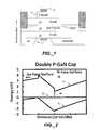
- FIG. 1is a schematic representation of a double p-type capped device.
- FIG. 2is a band diagram under the gate region of the double p-type capped device.
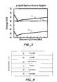
- FIG. 3is a band diagram in the access region of the double p-type capped device.
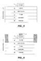
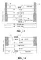
- FIGS. 4-13show intermediary structures created while forming the double p-type capped device.
- FIG. 14is a schematic representation a device with a regrown AlGaN layer surrounding a p-type cap.
- FIG. 15is a schematic representation a device with a dopant inducing layer in the access region.
- FIG. 16is a schematic representation of a device treated with a fluorine based plasma on both the Ga-face and the N-face.
- FIG. 17is a band diagram under the gate region of the fluorine treated device.
- FIG. 18is a band diagram in the access region of the fluorine treated device.
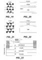
- FIG. 19is a GaN crystal structure with a Ga-face.
- FIG. 20is a schematic representation of a III-nitride type heterostructure of a Ga-face device.
- FIG. 21is a GaN crystal structure with an N-face.
- FIG. 22is a schematic representation of a III-nitride type heterostructure of an N-face device.
- FIG. 23is a schematic representation of an N-face device with a p-type cap under the gate.
- FIG. 24is a band diagram under the gate region of the N-face device with a p-type cap under the gate.
- FIG. 25is a schematic representation of a device with a layer of varying thickness in the access region.
- FIG. 26is a band diagram in the access region of the N-face device with a p-type cap under the gate.
- FIGS. 27-29show an exemplary method of forming an N-face enhancement mode device with a p-type cap.
- FIG. 30is a schematic representation of a device with a multi-compositional cap.
- FIG. 31is a band diagram under the gate region of the device with a multi-compositional cap.
- FIG. 32is a band diagram in the access region of the device with a multi-compositional cap.
- FIGS. 33-37show an exemplary method of forming the enhancement mode N-face device with the multi-compositional cap.
- FIG. 38is a schematic representation of a device that has been ion implanted in the access region.
- FIGS. 39-41illustrate p-type cap devices and structures.
- FIG. 42is a schematic representation of a device with a layer for selectively doping the access region.
- FIGS. 43-44are schematic representations of a device with a Fermi pinning layer.
- FIG. 45is a schematic representation of a device with a dielectric cap.
- FIG. 46is a schematic representation of a device with a dielectric passivation layer on the N-face.
- FIG. 47is a schematic representation of a device with a slant field plate.
- FIG. 48is a schematic representation of a device with a layer of AlN between the layers of the heterojunction.
- a Ga-face enhancement mode III-nitride deviceis formed as a lateral device having a gate 17 , source 18 and drain 19 , the lateral device formed on a Ga-face surface of the III-nitride device and gating on both the Ga and N-faces of the device.
- the Ga-faceis a Ga-polar face.
- the deviceincludes a p-type Al z GaN cap 11 on the Ga-face and a p-type Al y GaN cap layer (shown as p GaN layer 14 ) accessed from the N-face of the device, where 0 ⁇ y ⁇ 1 and 0 ⁇ z ⁇ 1.
- the p-type Al z GaN cap 11has a thickness of between about 1 nm and 100 nm, such as about 10 nm. In some embodiments, the p-type Al y GaN cap layer has a thickness of between about 1 nm and 30 nm, such as about 10 nm. In some embodiments, either of the p-type Al z GaN cap 11 or the p-type Al y GaN cap layer is a continuously graded layer, that is, includes more or less aluminum at different depths of the layer.
- the deviceincludes a GaN layer 15 on the N-face of the p GaN layer 14 .
- the GaN layer 15includes a recess which exposes the p GaN layer 14 and can have a thickness of between about 10 nm and 500 nm, such as about 50 nm.
- a GaN channel layer 13On an opposite side of the p GaN layer 14 is a GaN channel layer 13 , which can have a thickness of between about 1 nm and 50 nm, such as about 10 nm.
- the p-type Al z GaN cap 11is on the layer of Al x GaN 12 , in the gate region and under gate 17 .
- the break in the 2DEG indicator line under the gateshows that there is no charge under the gate at zero bias on the gate and that the device is an enhancement mode or normally off device. (A dashed line in each figure, other than FIGS. 20 and 22 , indicates the 2DEG.)
- Each of the III-nitride layerscan be epitaxially grown on one another.
- the Al x GaN/GaN layers 12 , 13are grown thin enough so that the surface pinning position of the p-type Al z GaN or GaN layers 11 , 14 depletes the 2DEG at the Al x GaN/GaN layer interface in the gate region.
- the Al x GaN/GaN layers 12 , 13are grown thin when the device includes a fully depleted p-type layer. If the device has a thick p-type layer on top, the barrier created by the p-type Al z GaN/Al x GaN junction depletes the 2DEG. Depleting the 2DEG from both surfaces increases the internal barrier and the threshold voltage.
- one of gates 17 , 17 ′is optional on the device.
- the polarization fields in the Al x GaN/GaN layers 12 , 13allows for the 2DEG at the Al x GaN/GaN interface in the access region.
- the thickness of the Al x GaN cap 12is controlled to maintain adequate 2DEG and a low on-resistance.
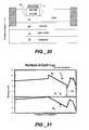
- the band diagrams of the double p-type cap device under the gate and the access regionshow the conduction band (E C ) and valence band (E V ) with respect to the Fermi level (E F ).
- the minimum distance 90 between the conduction band E C and the Fermi level E F at zero bias on the gatedefines the device's internal barrier.
- the internal barrier of the deviceis about 1 eV.
- the conduction band E ccrosses the Fermi level E F in the access region of the device, indicating that the device has a high 2DEG density in the access region and hence can achieve a low on-resistance.
- a GaN buffer layer 15 , a p-type GaN cap layer 14 (or p-type Al y GaN (0 ⁇ y ⁇ 1)), a GaN channel layer 13 , a Al x GaN layer 12 and a p-type Al z GaN cap layer 9are epitaxially grown on a substrate 16 .
- the exposed surface of the p-type Al z GaN cap layer 9 and the top surface of each layeris Ga-faced.
- the p-type Al z GaN cap layer 11is etched to define a gate region where the p-type Al z GaN cap 11 is located.
- a gate 17 with a schottky contact and source 18 and drain 19 with ohmic contactsare formed on the Ga-face to form an assembly.
- a passivation layer 23is applied to the exposed Ga-faces of the assembly.
- a bonding layer 24is applied to the passivation layer 23 .
- a carrier wafer 60is attached to the bonding layer 24 .
- the substrate 16is removed from the GaN layer 15 .
- an additional sacrificial layercan be included (not shown).
- This layercontains an etch stop layer which is not etched when the sacrificial layer is etched.
- the sacrificial layeris etched selectively to ensure a planar N-face GaN surface.
- the assemblyis then flipped over so that the N-face is accessible.
- the GaN buffer layer 15is etched to form a recess that allows for access to the p-type GaN cap layer 14 .
- a gate 17 ′is then deposited on the N-face of cap layer 14 within the recess and contacting the p-type GaN cap layer 14 .
- back side contactis made to the original front side source 18 and drain 19 ohmic contacts. Additionally, contact is made with the gate pad (not shown, because it is in the plane of the figure) and any other pads where contact is required.
- a layer of Al y GaN 20is grown in the access region surrounding the p-type cap.
- the layer of Al y GaN 20can further enhance the 2DEG and conductivity under the access region.
- the on-resistancemay be lower than in the device shown in FIG. 1 .
- the method of forming this deviceis similar to that described in FIG. 4-13 with the exception of selectively growing the layer of Al y GaN 20 after the etch of the p-type layer 11 .
- the access regionsare doped.
- An intermediary step of making the deviceis shown.
- the dopingis achieved by thermal diffusion of donor species into the access regions.
- a thin film dielectric 29 with a donor species, such as Si, SiO 2 or SiN x (in the case of Si dopant),is deposited onto the Ga-face access region of a III-nitride epitaxial layer structure.
- the thin film dielectric 29can either be applied to the Ga-face or the N-face of the device.
- the materialis annealed, such as at a temperature between about 300 and 900° C., which increases the 2DEG density in the access regions, thus resulting in lower on-resistance.
- multiple diffusionsare performed to mimic a lightly doped drain structure.
- the thin film dielectricis removed after the annealing process.
- an enhancement mode III-nitride device with gating on both the Ga and N-facesis shown where the device is fluorine treated.
- the Ga-faceis a Ga-polar face and the N-face is an N-polar face.
- the deviceincludes a region on both the Ga-face beneath the gate 17 and a region on an N-face beneath the gate region that has been treated with a fluorine compound.
- the fluorine treatmentcan be a fluorine based plasma treatment.
- a fluorine treatment on both the Ga-face and the N-faceincreases the internal barrier and the threshold voltage of the device.
- the structure under the gateis a layer of Al y GaN 25 on a GaN channel layer 13 on a layer of Al x GaN 21 , which is on a GaN buffer layer 15 .
- a recess in the GaN buffer layer 15exposes a portion of the layer of Al x GaN 21 .
- the recessis below the gate 17 and not below the access region.
- the exposed portion of the layer of Al x GaN 21is treated with a plasma of a fluorine compound.
- a gate region of the layer of Al y GaN 25is treated with the plasma. The fluorine-based treatment is not applied to the access regions.
- a bottom gate 17 ′is formed in the recess after the fluorine treatment of the N-face.
- the Al composition, x, in the Al x GaN layer 21is minimized, such as to between 0.1 to 0.3, for example, 0.1, and the thicknesses of the GaN channel layer 13 and the Al x GaN layer 21 are controlled to prevent depletion of the 2DEG or the formation of a parasitic channel at the interface between the layer of Al x GaN 21 and GaN buffer layer 15 .
- the GaN channel layer 13has a thickness of about 20 nm. In some embodiments, the thickness of the Al x GaN layer 21 is 10 nm.
- the deviceincludes an insulator 27 between the gate 17 and the layer of Al y GaN 25 and/or between the bottom gate 17 ′ and the layer of Al x GaN 21 .
- the insulatorcan have a thickness of between about 0.1 nm and 100 nm.
- one of the gates 17 , 17 ′is optional.
- the band diagram under the gate regions of a device with fluorine treatment under N-face and Ga-face gatesshows an internal barrier of 0.8 eV (at minimum distance 90 ).
- a possible mechanism of the shift in threshold voltage on which the band diagram is basedis that F ions act as acceptors.
- the fluorine-based plasma treatmentresults in high gate turn-on voltage and reduction of gate leakage current.
- the band diagram in the access regionshows a high 2DEG that will result in a low on-resistance.
- the fluorine based plasma treatmentis combined with the device shown in FIG. 1 , a p-type cap device.
- the fluorine based treatmentcan be applied to both the Ga-face and N-face surface.
- one surfacecan be p capped and the opposite surface can be treated with a fluorine treatment. This combination results in a device with a high internal barrier and a high threshold voltage while maintaining low on-resistance.
- a Ga-face devicehas a crystal structure with gallium atoms on its exposed face.
- a Ga-face structurecan be Ga-polar, semi-polar or a non-polar GaN structure.
- FIG. 20when a layer of AlGaN is deposited onto a layer of GaN, a 2DEG automatically forms because of the built-in sheet charge and electric fields in the heterostructure. Thus, Ga-face devices naturally tend to form depletion mode devices.
- the methods described aboveallow the Ga-faced devices to be enhancement mode devices. Many conventional III-nitride type devices are Ga-faced because a Ga-faced device can be easier to grow.
- N-face devicea device with a crystal structure with N atoms exposed or on its face is referred to as an N-face device.
- the devicecan be N-polar, semi-polar or non-polar.
- FIG. 22when a layer of AlGaN is deposited onto a layer of GaN, there is no spontaneous polarization in the heterostructure that causes the device to be a depletion mode device. Therefore, N-faced devices can be more easily made enhancement mode.
- an N-face deviceis formed with a p-type cap under the gate.
- the devicehas an epitaxial layer structure of a substrate 16 that includes a GaN layer 15 , an Al x GaN layer 43 and a GaN channel layer 41 (bottom to top).
- the 2DEGis in the GaN channel layer 41 .
- a p-type cap 11 of Al z GaN, 0 ⁇ z ⁇ 1,is grown thick enough, such as at least 10 Angstroms, or in some instances as thin as p-type material growth allows, so that the raised barrier height due to the surface pinning position of the p-Al z GaN and barrier induced by the p-Al z GaN/GaN hetero-interface depletes the 2DEG at the GaN channel layer 41 /Al x GaN layer 43 interface under the gate region at zero gate bias. Because the p-Al z GaN increases the gate barrier height, the gate turn-on voltage increases and the gate leakage current decreases.
- a thin, e.g., a layer less than 100 Angstroms, AlN layercan be included under the p-type Al z GaN cap and above the GaN channel 41 in the gate region. This AlN layer can also be within the p-type cap. In some embodiments the AlN layer is doped p-type or is an Al w GaN layer with a high Al composition (w>x).
- the GaN channel layer 41is reduced to 5 nm to increase the internal barrier and the threshold voltage of the device.
- the internal barrier of the deviceis at least 1.5 eV (at minimum distance 90 ).
- the GaN channel layer 41is thicker in the access region than in the gate region. Because the 2DEG density increases with the thickness of the GaN channel layer, the on-resistance of the device can be reduced by increasing the thickness of GaN channel layer 41 . Thus, the GaN channel layer 41 can be grown to surround the p-type Al z GaN cap 11 . The GaN channel layer 41 can also extend under the Al z GaN cap 11 , but it can be thicker in the access region, up to 500 nm, such as about 30 nm. The thin portion under the gate can be about 5 nm in thickness.
- the thick portion in the access regionallows for sufficient 2DEG at the GaN channel layer 41 /Al x GaN layer 43 interface to result in minimum resistance in the access region.
- the full thickness of the GaN channel layer 41is grown first and then subsequently etched away, followed by the selective regrowth of the p-type Al z GaN cap 11 .
- a thinner GaN channel layer 41is formed during the first structure growth and is then capped by a layer of Al z GaN, followed by etching the layer of Al z GaN outside the gate region, i.e., in the access region and the regrowth of the remainder of GaN channel layer 41 in the access region.
- FIG. 26the energy band diagram in the access region is shown. Without the high barrier of the p-Al z GaN cap 11 , polarization in these layers allow for a 2DEG at the GaN channel/Al x GaN interface outside the gate region.
- the p-type Al z GaN cap 11is doped, such as with Mg or other p-type dopant.
- the p-type Al z GaN cap 11is a graded layer where z changes gradually, such as from 0 to 0.5.
- zis 0.3 and has a thickness of about 5 nm.
- the GaN channel layer 41includes a small fraction of aluminum, thus forming a layer of Al y GaN, where y is less than 0.15. The small amount of Al can improve the breakdown voltage of the device.
- an N-face deviceis not necessarily as easy as growing a Ga-face device.
- FIGS. 27-29a method of forming an N-face device, such as the device shown on FIG. 23 , is described, wherein the original layers are grown as Ga-face layers and then flipped to realize the intended N-face device.
- an epitaxial layer structureis grown in substrate 50 .
- the epitaxial layer structureincludes a thick GaN layer 55 , an Al x GaN layer 43 , a GaN channel layer 41 , a p-type Al z GaN layer 9 , and a GaN buffer 52 , which are on the substrate 50 (from top to bottom).
- the epitaxial layer structureis grown as a Ga-face structure and is subsequently flipped.
- the thick GaN layer 55eventually will serve as the buffer layer of the N-face device.
- a carrier wafer 60is bonded onto the thick GaN layer 55 to form an assembly.
- the bondcan be a metal based bond or a dielectric bond or other suitable bond. If the carrier wafer 60 will eventually serve as the final substrate, the carrier wafer can be thermally conducting and electrically insulating. In some embodiments, the bond between the carrier wafer 60 and the thick GaN layer 55 is not conductive.
- the assemblyis flipped over so that the carrier wafer 60 is on the bottom of the device.
- the substrate 50is removed using a technique suitable for the substrate material, such as laser liftoff for sapphire substrates, lapping or plasma etching for SiC based substrates or wet or dry etching for silicon substrates.
- the GaN buffer layer 52is also removed, such as by a dry etch.
- the structureis now an N-face structure that is ready for completing to form the devices shown in FIGS. 27 and 30 .
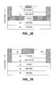
- a multi-compositional cap 65is formed under the gate of an N-face device.
- the epitaxial layer structure of the deviceis a channel layer of GaN 41 on a layer of Al z GaN 44 on GaN buffer layer 15 , which is on substrate 16 .
- the GaN channel layer 41is thicker in the access region than in the gate region.
- a cap 65is formed with either a graded composition of AlGaN or multiple layers of AlGaN, such as a layer of Al x GaN that is adjacent to the channel layer and a layer of Al y GaN that is adjacent to the gate 17 , where y>x.
- the polarization and bandgap differences in the multi-compositional AlGaN layersincrease the barrier height and deplete the 2DEG at the interface between the GaN channel layer 41 and the layer of Al z GaN 44 in the gate region at zero gate bias. As in FIG. 25 , reducing the GaN channel layer thickness in the gate region also increases the threshold voltage.
- the multi-compositional AlGaN capincreases the gate barrier height, the gate turn-on voltage increases and the gate leakage current decreases in the device.
- the multi-compositional cap in combination with the thinned GaN channel layer portion in the gate regioncan result in a device with at least a 1.4 eV internal barrier.
- the access region of the deviceshows a high 2DEG concentration that enables low on-resistance.
- the device in FIG. 30can be formed by starting with an epitaxial layer structure of a substrate 50 on which a GaN buffer layer 15 , a layer of Al z GaN 44 , a GaN channel layer 41 , a layer of Al x GaN 67 and a layer of Al y GaN 69 are formed (from bottom to top).
- the structureis an N-face device.
- the Al y GaN layer 69 and Al x GaN layer 67are then etched to form the cap 65 . Additional GaN material is regrown around the cap 65 , above the GaN channel 41 .
- the gate 17 , source 18 and drain 19 contactsthen are formed.
- a structure with a thick GaN channel layer 41 , a layer of Al z GaN 44 and a GaN layer 15are epitaxially grown on substrate 16 , as shown in FIG. 34 .
- the thick GaN channel layer 41is etched in the gate region and the cap 65 , comprising of the materials of the layer of Al x GaN 67 and the layer of Al y GaN 69 , is regrown (see FIG. 30 ).
- the multi-compositional cap devicecan also be formed by forming a Ga-face structure and flipping the structure.
- an epitaxial layer structureincluding a thick GaN layer 55 , a layer of Al z GaN 44 , a GaN channel layer 41 , a layer of Al x GaN 67 , a layer of Al y GaN 69 and a GaN buffer 52 are formed on the substrate 50 (from top to bottom).
- the epitaxial layer structureis grown as a Ga-face and is subsequently flipped.
- the thick GaN layer 55eventually will serve as the buffer layer of the N-face device.
- a carrier wafer 60is bonded onto the thick GaN layer 55 to form an assembly.
- the bondcan be a metal based bond or a dielectric bond. If the carrier wafer 60 will eventually serve as the final substrate, the carrier wafer can be thermally conducting and electrically insulating. However, the bond between the carrier wafer 60 and the thick GaN layer 55 is not conductive.
- the assemblyis flipped over so that the carrier wafer 60 is on the bottom of the device.
- the substrate 50is removed using a suitable method for the type of substrate, such as laser liftoff for sapphire substrates, lapping or plasma etching for SiC based substrates or wet or dry etching for silicon substrates.
- the GaN buffer layer 52is also removed, such as by a dry etch.
- the structureis now an N-face structure that is ready for completing to form the device shown in FIG. 30 .
- the layers of Al x GaN 67 and Al y GaN 69are omitted in the initial growth and the GaN channel layer 41 is the final desired thickness for the access region, when it is applied to the layer of Al x GaN 67 .
- the GaN channel layer 41is then etched in the gate region and the cap 65 is formed where the GaN channel layer material was removed.
- the device shown in FIG. 30is formed without the regrown GaN material on the GaN channel layer 41 . Thus, there is no recess in which the cap 65 is located.
- an N-face deviceis formed by ion implanting the access region with n-type dopant ions, such as Si.
- n-type dopant ionssuch as Si.
- the access region portion of the Al x GaN layer 21is ion implanted to increase the 2DEG density at the interface of the GaN channel layer 13 and the Al x GaN layer 21 , outside the gate region. The resulting band structure in these regions force the electrons from the dopant ions to fall in the 2DEG at the interface of the GaN channel layer 13 and the Al x GaN layer 21 .
- the p-type cap layeris a layer of Al y GaN 25 which extends from the source 18 to the drain 19 contacts.
- the layer GaN 31is etched in the gate region to form layer GaN 32 and a gate is deposited such that the layer of GaN 32 is surrounding the gate 17 and on the p-type cap layer of Al y GaN 25 .
- the layer of GaN 32is only in the access region and increases the 2DEG in that region.
- the cap layer of AlyGaN 25where not covered by the layer of GaN of the gate region, depletes the 2DEG to realize normally off operation.
- Source and drain contacts 18 , 19are deposited to complete the device, as shown in FIG. 39 .
- the devices shown in FIGS. 39 and 41can be formed by starting with a stack of a GaN layer 15 , a layer of Al x GaN 21 , a GaN channel layer 13 and a layer of p-type Al y GaN 25 , and a GaN layer 32 , all grown on N-face layers.
- the polarization provided by the layer of GaN 32 in this N-face structurecontributes to increasing the 2DEG.
- the layer of GaN 32has a thickness of at least 10 nm and thick enough to ensure charge in the access region. Referring back to FIG. 39 , the layer of GaN 32 is etched in the gate region and left to remain in the access region.
- a gate electrodeis deposited on the p-type Al y GaN layer 25 in the gate region.
- the etch back of the layer of GaN to form layer of GaN 32results in depletion of the 2DEG under the gate region, making the device normally off.
- Source 18 and drain 19 ohmic contactsare also deposited.
- an insulating layer 35is deposited, such as by MOCVD, PECVD, ICP, E-beam or other suitable deposition method, over the etched layer of GaN 32 and between the gate 17 and the layer of p-type Al y GaN 25 .
- the insulating layer 35can further reduce gate leakage current increase gate turn on voltage and provide passivation.
- the insulating layercan be deposited either before or after forming the ohmic contacts for the source 18 and drain 19 . If the insulating layer 35 is deposited before the formation of the ohmic contacts, portions of the layer can be removed or left in place where metallization is to be deposited for the ohmic contacts. Both the device of FIG. 39 and FIG. 41 device do not require a regrowth step.
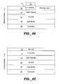
- an N-face deviceis formed that has a selectively doped access region.
- the access regionis doped by thermal diffusion of donor species from a dielectric (or other suitable) dopant diffusion layer 75 in the access region.
- the dopant diffusion layer 75can include donor species, such as Si, SiO 2 , SiN x and other suitable donor species.
- the dopant diffusion layer 75is annealed to cause the dopant (Si in case of Si, SiO x or SiN x ) to migrate into the device and increase the 2DEG density in the access regions, thereby causing the device to have a lower on-resistance.
- the thermal diffusioncan be carried out at any suitable temperature, for example between about 300 and 1000° C. To enhance the breakdown voltage of the device, multiple diffusions can be performed to mimic a lightly doped drain structure. In some embodiments, the dopant diffusion layer 75 is removed after annealing.
- a dielectric layer which functions as a Fermi level pinning layer 78is applied on the device.
- the pinning layer 78can be either doped or undoped.
- the pinning layer 78induces charge in the access region.
- the pinning layeris not only in the access region, but is also formed on the p-type Al z GaN cap 11 .
- the cap 11blocks any effects from the pinning layer 78 on the device in the gate region and thus the pinning can be on the cap without adversely causing a 2DEG in the gate region.
- the pinning layer 78can be a layer of SiN x , such as a layer of SiN x grown by MOCVD, PECVD, CATCVD or other suitable means, including a combination of various deposition techniques. SiN x on N-face or Ga-face III-nitride devices can pin the surface Fermi level close to the conduction band, resulting in high electron concentration and increased conductivity under the SiN x region.
- the pinning layer 78can be deposited at any suitable step in the fabrication sequence of the device, such as before the ohmic metal contacts are deposited or after. The pinning layer can be removed from the gate, source or drain contacts where electrical contact will be made.
- FIGS. 45-48show a variety of features that can be used with any of the devices described herein. Although the devices shown are N-face devices, the features can also be used with Ga-face devices.
- a SiN x cap 80can be applied to the N-face of the cap during an early stage of processing and is selectively removed at a desired step in the process.
- N-face III-nitride devicescan be more susceptible to damage than Ga-face III-nitride devices.
- the SiN x cap 80serves to protect the N-face surface from undesired damage during processing.
- the SiN x cap 80can be thin, such as less than 2000 Angstroms, for example, 100 Angstroms.
- part of the SiN x cap 80is left in the gate region to function as a gate insulator.
- a dielectric passivation layer 83is formed on an N-face device.
- the passivation layer 83can be SiN x or other suitable passivation material.
- the passivation materialcan be deposited by CVD, such as PECVD, MOCVD or ICP or by evaporation.
- an optional field plate 87is formed over the gate region to reduce the peak electric field and help trapping and breakdown voltage capacity. The field plate 87 can be terminated at the source or at the gate.
- a slant field plate 93can be applied to an N-face device.
- the slant field plate 93maximizes breakdown voltage.
- the slant field platecan be applied along with a dielectric passivation layer 83 .
- the slant field plate 93is integrated with the gate.
- a devicecan be formed with a gate insulator 96 and/or an AlN inter-layer 97 between the GaN channel layer 41 and the Al x GaN layer 43 .
- the gate insulator 96is between the gate and the top semiconductor layer, such as the p-type cap or the channel layer.
- the gate insulatorcan minimize gate leakage.
- the gate insulator 96is formed of a suitable insulating material, such as SiN x , SiO 2 or AlN.
- the layer of AlN 97 between the GaN channel layer 41 and the Al x GaN layer 43is thin, such as greater than 0 to about 30 Angstroms. This layer improves the mobility-2DEG density product, resulting in a device with lower resistance.
- III-nitride materialsare described, a modification of the material may be used in its place so long as the material is not modified in such a way to reverse the intended polarization, e.g., by hindering the 2DEG in an access region or by inducing charge in the gate region.
- GaNgallium-nitride
- small amounts of aluminum or indium, e.g., up to 15%, 10%, 5% or 2%may be included in the GaN layer without deviating from the scope of the disclosed methods and devices.
- AlGaN materialsare described, AlInGaN materials can be used in their place.
- any of the GaN materials that are describedcan be replaced by secondary, tertiary, or quaternary materials, which are based on varying the amounts of the III type material of AlInGaN, Al, In and Ga, from 0 to 1, or Al x In y Ga 1-x-y N.
- Al x GaN material0 ⁇ x ⁇ 1, Al x Ga 1-x N can be substituted.
- a subscript for a group III materialsuch as x, y or z, a different letter may be used in the claims.
- > or ⁇may be substituted by ⁇ or ⁇ , respectively and ⁇ or ⁇ can be substituted by > or ⁇ , respectively.
- the Al x GaN layer adjacent to the channel layer and responsible for forming a heterostructure with and 2DEG in the channel layercan be doped at least in part.
- the dopingis n-type.
- the GaN buffer layeris generally semi-insulating but in some embodiments may include a small portion, such as a portion furthest from the substrate side of the buffer layer, that is doped. This doping can be either n-type or p-type.
- the devices described hereincan be formed on a substrate of sapphire, silicon carbide (either Si-face or C-face), silicon, aluminum nitride, gallium nitride or zinc oxide.
- a transition layer or a nucleation layercan be formed on the substrate to facilitate the growth of the III-nitride layers.
- the nucleation layeris specific to the type of substrate used.
- a capis only in the gate region and not in the access region. However, in other embodiments, the cap extends across the access region as well.
- fluorine treatmentthroughout the specification. This treatment may result in fluorine doping in the semiconductor layers.
- the transistors described hereinare power transistors, which are capable of blocking at least 600 V, such as at least 900 V or at least 1200 V.
Landscapes
- Junction Field-Effect Transistors (AREA)
- Insulated Gate Type Field-Effect Transistor (AREA)
- Chemical & Material Sciences (AREA)
- Engineering & Computer Science (AREA)
- Materials Engineering (AREA)
Abstract
Description
- This application is a divisional application of U.S. patent application Ser. No. 13/019,150, entitled “Enhancement Mode Gallium Nitride Power Devices,” filed on Feb. 1, 2011, which is a divisional application of U.S. patent application Ser. No. 11/856,687, entitled “Enhancement Mode Gallium Nitride Power Devices,” filed on Sep. 17, 2007, now U.S. Pat. No. 7,915,643. The entire disclosure of both of the prior applications is hereby incorporated by reference.
- This disclosure is related to gallium nitride based semiconductor transistors.
- Gallium nitride (GaN) semiconductor devices, which are III-V or III-nitride type devices, are emerging as an attractive candidate for power semiconductor devices because the GaN devices are capable of carrying large currents and supporting high voltages. Such devices are also able to provide very low on-resistance and fast switching times. A high electron mobility transistor (HEMT) is one type power semiconductor device that can be fabricated based on GaN materials. As used herein, GaN materials that are suitable for transistors can include secondary, tertiary, or quaternary materials, which are based on varying the amounts of the III type material of AlInGaN, Al, In and Ga, from 0 to 1, or AlxInyGa1-x-yN. Further, GaN materials can include various polarities of GaN, such as Ga-polar, N-polar, semi-polar or non-polar. In particular, N-face material may be obtained from N-polar or semi-polar GaN.
- A GaN HEMT device can include a III-nitride semiconductor body with at least two III-nitride layers formed thereon. Different materials formed on the body or on a buffer layer causes the layers to have different band gaps. The different materials in the adjacent III-nitride layers also causes polarization, which contributes to a conductive two dimensional electron gas (2DEG) region near the junction of the two layers, specifically in the layer with the narrower band gap. One of the layers through which current is conducted is the channel layer. Herein, the narrower band gap layer in which the current carrying channel, or the 2DEG is located is referred to as the channel layer. The device also includes a gate electrode, a schottky contact and an ohmic source and drain electrodes on either side of the gate. The region between the gate and drain and the gate and source, which allows for current to be conducted through the device, is the access region.
- The III-nitride layers that cause polarization typically include a barrier layer of AlGaN adjacent to a layer of GaN to induce the 2DEG, which allows charge to flow through the device. This barrier layer may be doped or undoped. In some cases, doping of the barrier layer may add to channel charge and it may also help in dispersion control. Because of the 2DEG typically existing under the gate at zero gate bias, most III-nitride devices are normally on or depletion mode devices. If the 2DEG is depleted, i.e., removed, below the gate at zero applied gate bias, the device can be an enhancement mode or normally off device.
- Enhancement mode or normally off III-nitride type devices are desirable for power devices, because of the added safety they provide. An enhancement mode device requires a positive bias applied at the gate in order to conduct current. Although methods of forming III-nitride enhancement type devices are known, improved methods of depleting the 2DEG from under the gate in the channel layer are desirable.
- Devices are described that are enhancement mode devices with low off state leakage current as well as low on resistance. This is achieved in structures that result in not only depleting the 2DEG from under the gate region, but also have a high barrier to current flow under the gate region in the off state while ensuring that the region outside the gate, i.e., the access region, remains highly conductive.
- In one aspect, a method of forming an N-face enhancement mode high electron mobility transistor device is described. The method includes forming on a substrate a Ga-faced sacrificial layer, forming a cap layer on the sacrificial layer, forming a GaN channel layer on the cap layer, forming an AlxGaN layer on the channel layer, wherein 0≦x≦1, forming a buffer layer on the AlxGaN layer, bonding a carrier wafer on the buffer layer to form a stack, removing the substrate and the sacrificial layer from the stack to form an N-faced assembly of layers and forming a gate, source and drain on the N-faced assembly of layers.
- In another aspect, a normally off III-nitride HEMT device is described. The device includes a gate, a source and a drain and an access region formed of a III-nitride material between either the source and the gate or the drain and the gate. In the access region the sheet resistance is less than 750 ohms/square. The device has an internal barrier under the gate of at least 0.5 eV, such as at least 1 eV, when no voltage is applied to the gate. The device is capable of supporting a 2DEG charge density under the gate of greater than 1×10¹²/cm2in the on state.
- In yet another aspect, a Ga-face enhancement mode high electrode mobility transistor device is described. The device includes a GaN buffer layer, a p-type bottom cap on the GaN buffer layer, wherein the GaN buffer layer has an aperture exposing the bottom cap, a GaN channel layer on an opposite side of the bottom cap from the GaN buffer layer, an AlxGaN layer on an opposite side of the GaN channel layer from the cap layer, a p-type top cap on an opposite side of the AlxGaN layer from the channel layer and a gate adjacent to the top cap.
- In yet another aspect, a method of making a Ga-face enhancement mode high electrode mobility transistor device is described. The method includes forming a structure including the GaN buffer, GaN channel layer and AlxGaN layer, forming the p-type top cap on the AlxGaN layer, forming the gate adjacent to the p-type top cap, applying a passivation layer over the p-type top cap and AlxGaN layer, bonding a carrier wafer onto the passivation layer and forming the aperture in the GaN buffer layer.
- In another aspect, a Ga-face enhancement mode high electrode mobility transistor device is described. The device has a GaN buffer layer, an AlxGaN layer on the GaN buffer layer, wherein the GaN buffer layer has an aperture exposing the AlxGaN layer, a GaN channel layer on an opposite side of the AlxGaN layer from the GaN buffer layer, an AlyGaN layer on an opposite side of the GaN channel layer from the AlxGaN layer, wherein a gate region of the AlyGaN layer is treated with fluorine and an upper gate adjacent to the gate region. The fluorine treatment can include a treatment with a fluorine containing plasma.
- In yet another aspect, a method of forming a Ga-face enhancement mode high electrode mobility transistor device is described. The method includes forming a structure of the GaN buffer layer, the AlxGaN layer on the GaN buffer layer, wherein the GaN buffer layer has an aperture exposing a portion of the AlxGaN layer, a GaN channel layer on an opposite side of the AlxGaN layer from the GaN buffer layer and an AlyGaN layer on an opposite side of the GaN channel layer from the AlxGaN layer, treating the exposed portion of the AlxGaN layer with a fluorine containing compound and treating the gate region of the AlyGaN layer with the fluorine containing compound.
- In yet another aspect, a structure that is part of an enhancement mode high electrode mobility transistor device is described. The structure includes a GaN buffer layer on a substrate. On the buffer layer is a heterostructure region and 2DEG formed by a layer of AlGaN, with an aluminum composition between 0 and 1 or equal to 1 and a GaN channel layer. A cap is on the layers that form the heterostructure region. A dielectric layer is formed on the layers that form the heterostructure region and adjacent to the cap. A gate on the cap. The device is an N-face device.
- In one aspect, an N-face enhancement mode high electron mobility transistor device is described. The device includes a substrate and a heterostructure region and 2DEG region formed by a layer of AlGaN with an aluminum composition between 0 and 1 or equal to 1 and a GaN channel layer. The heterostructure region is on the substrate. The GaN channel layer has a Ga-face adjacent to the layer of AlxGaN. A cap is in a recess of an N-face of the channel layer. The cap does not overlie an access region of the device. A gate is formed on the cap. A source and drain are on laterally opposing sides of the cap.
- Embodiments of the devices and methods described herein may include one or more of the following features. A GaN channel layer on the cap layer can be a channel layer of GaN with up to 15% Al in the GaN. The cap layer can include p-type AlzGaN and a method of forming a device can further include etching the p-type AlzGaN to form a p-type AlzGaN cap, where forming a gate includes forming the gate on the p-type AlzGaN cap. Forming the channel layer and forming the AlxGaN layer on the channel layer can form a region of a first 2DEG charge, a method can further include forming a layer surrounding the p-type AlzGaN cap, the layer surrounding the p-type AlzGaN cap and the channel layer together having a net 2DEG charge that is greater than the first 2DEG charge. Forming a layer surrounding the p-type AlzGaN cap can include forming a layer of AlyGaN, wherein y<x. Forming a cap layer of p-type AlzGaN can include forming the cap layer to have a thickness of at least 50 Angstroms, with 0<z<1. Forming a channel layer of GaN can comprise forming a channel layer having a thickness less than 300 Angstroms under the gate region. Forming a GaN channel layer can include forming a channel layer having a thickness about 50 Angstroms. A device can have a 2DEG charge that is depleted under the gate and can have an internal barrier that is greater than 0.5 eV, such as at least 1 eV. The channel layer can be AlzGaN, 0.05<z<0.15. Forming the cap layer can include forming a multi-compositional cap layer, wherein a first layer of the cap layer comprises AlxGaN and a second layer of the cap layer comprises of AlyGaN, wherein the second layer is formed prior to the first layer being formed and y>x. A method of forming a device can include etching the multi-compositional cap layer to form a multi-compositional cap and forming a layer of GaN surrounding the multi-compositional cap. The surrounding GaN layer can be formed using selective regrowth. The multi-compositional cap layer can change from AlxGaN to AlyGaN in a continuous or discontinuous manner.
- The carrier layer can be thermally conducting and electrically insulating. Removing the substrate can include using laser liftoff, lapping, wet etching or dry etching. The method can further include plasma treating a portion of an N-face that corresponds to a location in which the gate is subsequently formed. The channel layer and the layer of AlxGaN can form a hetero structure with a resulting 2DEG region in the channel layer and the method can further include implanting ions in the access region of the wider bandgap layer to increase net 2DEG charge. The device can have an access region, and the method can further include doping the access region by thermal diffusion of donor species. An N-face layer can be passivated after the N-face layer is exposed. In a device where the structure is built upside down, an AlN layer can be formed on the channel layer prior to forming the layer of AlxGaN. The access region can be selectively doped in the channel layer, such as by thermal diffusion of donor species. A dielectric layer can be formed on a surface of the access region to form a pinning layer. The device can be capable of blocking at least 600 V, 900V or 1200 V. The device can have an on-resistance of less than 15 mohm-cm2, less than 10 mohm-cm2, 3 mohm-cm2or less than 2 mohm-cm2. A top cap can be formed of p-type AlzGaN. The top cap may comprise a thin AlN layer, e.g., less than 20 Angstroms, or a high Al composition AlGaN layer, e.g., where the Al composition is greater than 50%, to prevent or reduce gate leakage. A bottom cap can be formed of p-type GaN. The bottom cap can be formed of AlyGaN, wherein y varies from one surface to an opposite surface of the bottom cap. The AlxGaN layer can have a thickness of less than 500 Angstroms. The channel layer can have a thickness of less than 300 Angstroms, such as less than 100 Angstroms, under the gate region. A gate can be in an aperture and contacting the bottom cap. A layer of AlyGaN can laterally surround the top cap, where y>x. The device can have an internal barrier of at least 0.5 eV, such as at least 1 eV when no voltage is applied to the gate. A gate can be formed in the aperture in the GaN buffer layer. The AlxGaN layer exposed by an aperture can be doped with fluorine. A lower gate can be within an aperture exposing the AlxGaN layer. A p-type cap layer can be between the upper gate and the AlyGaN layer. A p-type cap layer can be between the lower gate and the AlxGaN layer. An insulator layer can be between the lower gate and the AlxGaN layer. An insulator layer can be between the upper gate and the AlyGaN layer. The device can have an internal barrier of at least 0.5 eV, such as at least 1 eV, when no voltage is applied to the gate. An insulator can be between the upper gate and the gate region. A cap can be a p-type cap. The cap can be a combination of p-type AlGaN layer and an AlN layer. The cap can include AlyGaN and AlxGaN, the AlyGaN is closer to the gate than the AlxGaN is and y>x. The AlyGaN and AlxGaN can be doped p-type. The channel layer can be adjacent to the cap. The dielectric layer can be a dopant diffusion layer and donor species in the dopant diffusion layer can increase 2DEG density in the access region. The dielectric layer can be on a side of the cap opposite to the channel layer. The channel layer can be adjacent to the cap and can have an N-face adjacent to the cap. The dielectric layer can form a pinning layer and can induce charge in the access region. A layer of AlN can be between the layer of AlGaN forming the heterostructure and the 2DEG and the GaN channel layer. A slant field plate can be on the gate. The dielectric layer can be between the cap layer and the gate. The GaN channel layer can laterally surround a gate region in which the gate is located. The cap can be a p-type AlzGaN. The cap can include p-type AlzGaN and AlN layers. The cap can include AlyGaN and AlxGaN, where the AlyGaN is closer to the gate than the AlxGaN is and y>x. The AlyGaN and AlxGaN can be doped p-type. The cap can include AlyGaN and AlxGaN, where the AlyGaN is closer to the gate than the AlxGaN is, AlyGaN and AlxGaN are doped p-type and x>y. An access region between the gate and source and between the gate and drain can be ion implanted. An insulating layer can be disposed between the gate and the cap. A dielectric passivation layer can be over at least the access region.
- Implementations of the methods and devices described herein can include one or more of the following advantages. High performance normally off devices with high positive threshold voltage are achieved. The positive threshold voltage can be adjusted by depositing an insulator of varying thickness on a device. However, high performance normally off devices require a large internal barrier that is not easily adjusted by merely depositing a thick insulator. A device can be formed with a high barrier, which determines the off state leakage current when the device is off. The internal barrier under the gate can be greater than 1 eV. The device may have a threshold voltage that is between about 1-3 volts. A device with a high internal barrier under the gate region can be formed while ensuring adequate charge or 2DEG in the access regions. The characteristics of the gate and access region can be independently controlled. Thus, a high internal barrier, high threshold voltage and low access region-resistance (high access region conductance) can simultaneously be achieved.
- The details of one or more embodiments of the invention are set forth in the accompanying drawings and the description below. Other features, objects, and advantages of the invention will be apparent from the description and drawings, and from the claims.
FIG. 1 is a schematic representation of a double p-type capped device.FIG. 2 is a band diagram under the gate region of the double p-type capped device.FIG. 3 is a band diagram in the access region of the double p-type capped device.FIGS. 4-13 show intermediary structures created while forming the double p-type capped device.FIG. 14 is a schematic representation a device with a regrown AlGaN layer surrounding a p-type cap.FIG. 15 is a schematic representation a device with a dopant inducing layer in the access region.FIG. 16 is a schematic representation of a device treated with a fluorine based plasma on both the Ga-face and the N-face.FIG. 17 is a band diagram under the gate region of the fluorine treated device.FIG. 18 is a band diagram in the access region of the fluorine treated device.FIG. 19 is a GaN crystal structure with a Ga-face.FIG. 20 is a schematic representation of a III-nitride type heterostructure of a Ga-face device.FIG. 21 is a GaN crystal structure with an N-face.FIG. 22 is a schematic representation of a III-nitride type heterostructure of an N-face device.FIG. 23 is a schematic representation of an N-face device with a p-type cap under the gate.FIG. 24 is a band diagram under the gate region of the N-face device with a p-type cap under the gate.FIG. 25 is a schematic representation of a device with a layer of varying thickness in the access region.FIG. 26 is a band diagram in the access region of the N-face device with a p-type cap under the gate.FIGS. 27-29 show an exemplary method of forming an N-face enhancement mode device with a p-type cap.FIG. 30 is a schematic representation of a device with a multi-compositional cap.FIG. 31 is a band diagram under the gate region of the device with a multi-compositional cap.FIG. 32 is a band diagram in the access region of the device with a multi-compositional cap.FIGS. 33-37 show an exemplary method of forming the enhancement mode N-face device with the multi-compositional cap.FIG. 38 is a schematic representation of a device that has been ion implanted in the access region.FIGS. 39-41 illustrate p-type cap devices and structures.FIG. 42 is a schematic representation of a device with a layer for selectively doping the access region.FIGS. 43-44 are schematic representations of a device with a Fermi pinning layer.FIG. 45 is a schematic representation of a device with a dielectric cap.FIG. 46 is a schematic representation of a device with a dielectric passivation layer on the N-face.FIG. 47 is a schematic representation of a device with a slant field plate.FIG. 48 is a schematic representation of a device with a layer of AlN between the layers of the heterojunction.- Like reference symbols in the various drawings indicate like elements.
- Referring to
FIG. 1 , a Ga-face enhancement mode III-nitride device is formed as a lateral device having agate 17,source 18 anddrain 19, the lateral device formed on a Ga-face surface of the III-nitride device and gating on both the Ga and N-faces of the device. In some embodiments, the Ga-face is a Ga-polar face. The device includes a p-type AlzGaN cap11 on the Ga-face and a p-type AlyGaN cap layer (shown as p GaN layer14) accessed from the N-face of the device, where 0<y<1 and 0<z<1. In some embodiments, the p-type AlzGaN cap11 has a thickness of between about 1 nm and 100 nm, such as about 10 nm. In some embodiments, the p-type AlyGaN cap layer has a thickness of between about 1 nm and 30 nm, such as about 10 nm. In some embodiments, either of the p-type AlzGaN cap11 or the p-type AlyGaN cap layer is a continuously graded layer, that is, includes more or less aluminum at different depths of the layer. The device includes aGaN layer 15 on the N-face of thep GaN layer 14. TheGaN layer 15 includes a recess which exposes thep GaN layer 14 and can have a thickness of between about 10 nm and 500 nm, such as about 50 nm. - On an opposite side of the
p GaN layer 14 is aGaN channel layer 13, which can have a thickness of between about 1 nm and 50 nm, such as about 10 nm. A layer of AlxGaN12 adjacent to theGaN channel layer 13 and opposite to the p-typeGaN cap layer 14 contributes to the 2DEG in theGaN channel layer 13. The p-type AlzGaN cap11 is on the layer of AlxGaN12, in the gate region and undergate 17. The break in the 2DEG indicator line under the gate, shows that there is no charge under the gate at zero bias on the gate and that the device is an enhancement mode or normally off device. (A dashed line in each figure, other thanFIGS. 20 and 22 , indicates the 2DEG.) Each of the III-nitride layers can be epitaxially grown on one another. - In some embodiments, the AlxGaN/GaN layers12,13 are grown thin enough so that the surface pinning position of the p-type AlzGaN or GaN layers11,14 depletes the 2DEG at the AlxGaN/GaN layer interface in the gate region. For example, the AlxGaN/GaN layers12,13 are grown thin when the device includes a fully depleted p-type layer. If the device has a thick p-type layer on top, the barrier created by the p-type AlzGaN/AlxGaN junction depletes the 2DEG. Depleting the 2DEG from both surfaces increases the internal barrier and the threshold voltage. The presence of high p-AlxGaN or GaN barriers also results in high gate turn-on voltage and reduction of gate leakage current. Additional insulating layers may be applied between the gates (17 or17′) and the respective p-type layers (11 and14).
- In some embodiments, one of
gates - Without the p-type AlzGaN cap11, the polarization fields in the AlxGaN/GaN layers12,13 allows for the 2DEG at the AlxGaN/GaN interface in the access region. Thus, the thickness of the AlxGaN cap12 is controlled to maintain adequate 2DEG and a low on-resistance.
- Referring to
FIGS. 2-3 , the band diagrams of the double p-type cap device under the gate and the access region, respectively, show the conduction band (EC) and valence band (EV) with respect to the Fermi level (EF). In the band diagram, theminimum distance 90 between the conduction band ECand the Fermi level EFat zero bias on the gate defines the device's internal barrier. The internal barrier of the device is about 1 eV. Referring toFIG. 3 , the conduction band Eccrosses the Fermi level EFin the access region of the device, indicating that the device has a high 2DEG density in the access region and hence can achieve a low on-resistance. - Referring to
FIGS. 4-13 , the method of forming a device with a p-type cap on both sides is described. Referring toFIG. 4 , aGaN buffer layer 15, a p-type GaN cap layer14 (or p-type AlyGaN (0<y<1)), aGaN channel layer 13, a AlxGaN layer12 and a p-type AlzGaN cap layer 9 are epitaxially grown on asubstrate 16. The exposed surface of the p-type AlzGaN cap layer 9 and the top surface of each layer is Ga-faced. Referring toFIG. 5 , the p-type AlzGaN cap layer 11 is etched to define a gate region where the p-type AlzGaN cap11 is located. Referring toFIG. 6 , agate 17 with a schottky contact andsource 18 and drain19 with ohmic contacts are formed on the Ga-face to form an assembly. Referring toFIG. 7 , apassivation layer 23 is applied to the exposed Ga-faces of the assembly. Referring toFIG. 8 , abonding layer 24 is applied to thepassivation layer 23. Referring toFIG. 9 , acarrier wafer 60 is attached to thebonding layer 24. Referring toFIG. 10 , thesubstrate 16 is removed from theGaN layer 15. Within the GaN buffer layer an additional sacrificial layer can be included (not shown). This layer contains an etch stop layer which is not etched when the sacrificial layer is etched. When the sacrificial layer is used, after etching the substrate the sacrificial layer is etched selectively to ensure a planar N-face GaN surface. Referring toFIG. 11 , the assembly is then flipped over so that the N-face is accessible. Referring toFIG. 12 , theGaN buffer layer 15 is etched to form a recess that allows for access to the p-typeGaN cap layer 14. Agate 17′ is then deposited on the N-face ofcap layer 14 within the recess and contacting the p-typeGaN cap layer 14. Referring toFIG. 13 , back side contact is made to the originalfront side source 18 and drain19 ohmic contacts. Additionally, contact is made with the gate pad (not shown, because it is in the plane of the figure) and any other pads where contact is required. - Referring to
FIG. 14 , in an alternative embodiment of the device ofFIG. 1 , a layer of AlyGaN20, where y>x, is grown in the access region surrounding the p-type cap. The layer of AlyGaN20 can further enhance the 2DEG and conductivity under the access region. Thus the on-resistance may be lower than in the device shown inFIG. 1 . The method of forming this device is similar to that described inFIG. 4-13 with the exception of selectively growing the layer of AlyGaN20 after the etch of the p-type layer 11. - Referring to
FIG. 15 , in yet another variation of the device ofFIG. 1 , the access regions are doped. An intermediary step of making the device is shown. The doping is achieved by thermal diffusion of donor species into the access regions. Athin film dielectric 29 with a donor species, such as Si, SiO2or SiNx(in the case of Si dopant), is deposited onto the Ga-face access region of a III-nitride epitaxial layer structure. Thethin film dielectric 29 can either be applied to the Ga-face or the N-face of the device. The material is annealed, such as at a temperature between about 300 and 900° C., which increases the 2DEG density in the access regions, thus resulting in lower on-resistance. In some embodiments, multiple diffusions are performed to mimic a lightly doped drain structure. In some embodiments, the thin film dielectric is removed after the annealing process. - Referring to
FIG. 16 , another embodiment of an enhancement mode III-nitride device with gating on both the Ga and N-faces is shown where the device is fluorine treated. In some embodiments, the Ga-face is a Ga-polar face and the N-face is an N-polar face. The device includes a region on both the Ga-face beneath thegate 17 and a region on an N-face beneath the gate region that has been treated with a fluorine compound. The fluorine treatment can be a fluorine based plasma treatment. A fluorine treatment on both the Ga-face and the N-face increases the internal barrier and the threshold voltage of the device. - The structure under the gate is a layer of AlyGaN25 on a
GaN channel layer 13 on a layer of AlxGaN21, which is on aGaN buffer layer 15. A recess in theGaN buffer layer 15 exposes a portion of the layer of AlxGaN21. The recess is below thegate 17 and not below the access region. The exposed portion of the layer of AlxGaN21 is treated with a plasma of a fluorine compound. Similarly, a gate region of the layer of AlyGaN25 is treated with the plasma. The fluorine-based treatment is not applied to the access regions. - In some embodiments, a
bottom gate 17′ is formed in the recess after the fluorine treatment of the N-face. In some embodiments, the Al composition, x, in the AlxGaN layer21 is minimized, such as to between 0.1 to 0.3, for example, 0.1, and the thicknesses of theGaN channel layer 13 and the AlxGaN layer21 are controlled to prevent depletion of the 2DEG or the formation of a parasitic channel at the interface between the layer of AlxGaN21 andGaN buffer layer 15. In some embodiments, theGaN channel layer 13 has a thickness of about 20 nm. In some embodiments, the thickness of the AlxGaN layer21 is 10 nm. Optionally, the device includes aninsulator 27 between thegate 17 and the layer of AlyGaN25 and/or between thebottom gate 17′ and the layer of AlxGaN21. The insulator can have a thickness of between about 0.1 nm and 100 nm. In some embodiments, one of thegates - Referring to
FIG. 17 , the band diagram under the gate regions of a device with fluorine treatment under N-face and Ga-face gates shows an internal barrier of 0.8 eV (at minimum distance90). A possible mechanism of the shift in threshold voltage on which the band diagram is based is that F ions act as acceptors. The fluorine-based plasma treatment results in high gate turn-on voltage and reduction of gate leakage current. Referring toFIG. 18 , the band diagram in the access region shows a high 2DEG that will result in a low on-resistance. - In some embodiments, the fluorine based plasma treatment is combined with the device shown in
FIG. 1 , a p-type cap device. The fluorine based treatment can be applied to both the Ga-face and N-face surface. Alternatively, one surface can be p capped and the opposite surface can be treated with a fluorine treatment. This combination results in a device with a high internal barrier and a high threshold voltage while maintaining low on-resistance. - Referring to
FIG. 19 , a number of the devices described above are formed as Ga-face devices. A Ga-face device has a crystal structure with gallium atoms on its exposed face. A Ga-face structure can be Ga-polar, semi-polar or a non-polar GaN structure. Referring toFIG. 20 , when a layer of AlGaN is deposited onto a layer of GaN, a 2DEG automatically forms because of the built-in sheet charge and electric fields in the heterostructure. Thus, Ga-face devices naturally tend to form depletion mode devices. The methods described above allow the Ga-faced devices to be enhancement mode devices. Many conventional III-nitride type devices are Ga-faced because a Ga-faced device can be easier to grow. - Referring to
FIG. 21 , a device with a crystal structure with N atoms exposed or on its face is referred to as an N-face device. The device can be N-polar, semi-polar or non-polar. Referring toFIG. 22 , when a layer of AlGaN is deposited onto a layer of GaN, there is no spontaneous polarization in the heterostructure that causes the device to be a depletion mode device. Therefore, N-faced devices can be more easily made enhancement mode. - Referring to
FIG. 23 , an N-face device is formed with a p-type cap under the gate. The device has an epitaxial layer structure of asubstrate 16 that includes aGaN layer 15, an AlxGaN layer43 and a GaN channel layer41 (bottom to top). The 2DEG is in theGaN channel layer 41. A p-type cap 11 of AlzGaN, 0<z<1, is grown thick enough, such as at least 10 Angstroms, or in some instances as thin as p-type material growth allows, so that the raised barrier height due to the surface pinning position of the p-AlzGaN and barrier induced by the p-AlzGaN/GaN hetero-interface depletes the 2DEG at theGaN channel layer 41/AlxGaN layer43 interface under the gate region at zero gate bias. Because the p-AlzGaN increases the gate barrier height, the gate turn-on voltage increases and the gate leakage current decreases. To further reduce gate leakage, a thin, e.g., a layer less than 100 Angstroms, AlN layer can be included under the p-type AlzGaN cap and above theGaN channel 41 in the gate region. This AlN layer can also be within the p-type cap. In some embodiments the AlN layer is doped p-type or is an AlwGaN layer with a high Al composition (w>x). - In some embodiments, the
GaN channel layer 41 is reduced to5 nm to increase the internal barrier and the threshold voltage of the device. Referring toFIG. 24 , the internal barrier of the device is at least 1.5 eV (at minimum distance90). - Referring to
FIG. 25 , in some embodiments, theGaN channel layer 41 is thicker in the access region than in the gate region. Because the 2DEG density increases with the thickness of the GaN channel layer, the on-resistance of the device can be reduced by increasing the thickness ofGaN channel layer 41. Thus, theGaN channel layer 41 can be grown to surround the p-type AlzGaN cap11. TheGaN channel layer 41 can also extend under the AlzGaN cap11, but it can be thicker in the access region, up to 500 nm, such as about 30 nm. The thin portion under the gate can be about 5 nm in thickness. - Reducing the thickness of the GaN layer under the gate increases the barrier under the gate and hence, the threshold voltage. The thick portion in the access region allows for sufficient 2DEG at the
GaN channel layer 41/AlxGaN layer43 interface to result in minimum resistance in the access region. In some embodiments, the full thickness of theGaN channel layer 41 is grown first and then subsequently etched away, followed by the selective regrowth of the p-type AlzGaN cap11. In other embodiments, a thinnerGaN channel layer 41 is formed during the first structure growth and is then capped by a layer of AlzGaN, followed by etching the layer of AlzGaN outside the gate region, i.e., in the access region and the regrowth of the remainder ofGaN channel layer 41 in the access region. Referring toFIG. 26 , the energy band diagram in the access region is shown. Without the high barrier of the p-AlzGaN cap11, polarization in these layers allow for a 2DEG at the GaN channel/AlxGaN interface outside the gate region. - In alternative embodiments to the device shown in
FIGS. 23 and 25 , the p-type AlzGaN cap11 is doped, such as with Mg or other p-type dopant. In some embodiments, the p-type AlzGaN cap11 is a graded layer where z changes gradually, such as from 0 to 0.5. In some embodiments, in the p-type AlzGaN cap11, z is 0.3 and has a thickness of about 5 nm. In some embodiments, theGaN channel layer 41 includes a small fraction of aluminum, thus forming a layer of AlyGaN, where y is less than 0.15. The small amount of Al can improve the breakdown voltage of the device. - As noted above, formation of an N-face device is not necessarily as easy as growing a Ga-face device. Referring to
FIGS. 27-29 , a method of forming an N-face device, such as the device shown onFIG. 23 , is described, wherein the original layers are grown as Ga-face layers and then flipped to realize the intended N-face device. Referring toFIG. 27 , an epitaxial layer structure is grown insubstrate 50. The epitaxial layer structure includes athick GaN layer 55, an AlxGaN layer43, aGaN channel layer 41, a p-type AlzGaN layer9, and aGaN buffer 52, which are on the substrate50 (from top to bottom). The epitaxial layer structure is grown as a Ga-face structure and is subsequently flipped. Thus, thethick GaN layer 55 eventually will serve as the buffer layer of the N-face device. - Referring to
FIG. 28 , acarrier wafer 60 is bonded onto thethick GaN layer 55 to form an assembly. The bond can be a metal based bond or a dielectric bond or other suitable bond. If thecarrier wafer 60 will eventually serve as the final substrate, the carrier wafer can be thermally conducting and electrically insulating. In some embodiments, the bond between thecarrier wafer 60 and thethick GaN layer 55 is not conductive. - Referring to
FIG. 29 , the assembly is flipped over so that thecarrier wafer 60 is on the bottom of the device. Thesubstrate 50 is removed using a technique suitable for the substrate material, such as laser liftoff for sapphire substrates, lapping or plasma etching for SiC based substrates or wet or dry etching for silicon substrates. TheGaN buffer layer 52 is also removed, such as by a dry etch. The structure is now an N-face structure that is ready for completing to form the devices shown inFIGS. 27 and 30 . - Referring to
FIG. 30 , in some embodiments, amulti-compositional cap 65 is formed under the gate of an N-face device. The epitaxial layer structure of the device is a channel layer ofGaN 41 on a layer of AlzGaN44 onGaN buffer layer 15, which is onsubstrate 16. TheGaN channel layer 41 is thicker in the access region than in the gate region. In the gate region, acap 65 is formed with either a graded composition of AlGaN or multiple layers of AlGaN, such as a layer of AlxGaN that is adjacent to the channel layer and a layer of AlyGaN that is adjacent to thegate 17, where y>x. In some embodiments, x=0.3 and y=0.5, and each of AlxGaN and AlyGaN are 5 nm thick. If the multi-compositional cap is graded, the grading can change from x to y in a continuous or discontinuous manner. The polarization and bandgap differences in the multi-compositional AlGaN layers increase the barrier height and deplete the 2DEG at the interface between theGaN channel layer 41 and the layer of AlzGaN44 in the gate region at zero gate bias. As inFIG. 25 , reducing the GaN channel layer thickness in the gate region also increases the threshold voltage. Further, because the multi-compositional AlGaN cap increases the gate barrier height, the gate turn-on voltage increases and the gate leakage current decreases in the device. Referring toFIG. 31 , the multi-compositional cap in combination with the thinned GaN channel layer portion in the gate region can result in a device with at least a 1.4 eV internal barrier. Referring toFIG. 32 , the access region of the device shows a high 2DEG concentration that enables low on-resistance. - Referring to
FIG. 33 , the device inFIG. 30 can be formed by starting with an epitaxial layer structure of asubstrate 50 on which aGaN buffer layer 15, a layer of AlzGaN44, aGaN channel layer 41, a layer of AlxGaN67 and a layer of AlyGaN69 are formed (from bottom to top). The structure is an N-face device. The AlyGaN layer69 and AlxGaN layer67 are then etched to form thecap 65. Additional GaN material is regrown around thecap 65, above theGaN channel 41. Thegate 17,source 18 and drain19 contacts then are formed. Alternatively, a structure with a thickGaN channel layer 41, a layer of AlzGaN44 and aGaN layer 15 are epitaxially grown onsubstrate 16, as shown inFIG. 34 . The thickGaN channel layer 41 is etched in the gate region and thecap 65, comprising of the materials of the layer of AlxGaN67 and the layer of AlyGaN69, is regrown (seeFIG. 30 ). - Similar to the method shown in
FIGS. 27-29 , the multi-compositional cap device can also be formed by forming a Ga-face structure and flipping the structure. Referring toFIG. 35 , an epitaxial layer structure including athick GaN layer 55, a layer of AlzGaN44, aGaN channel layer 41, a layer of AlxGaN67, a layer of AlyGaN69 and aGaN buffer 52 are formed on the substrate50 (from top to bottom). The epitaxial layer structure is grown as a Ga-face and is subsequently flipped. Thus, thethick GaN layer 55 eventually will serve as the buffer layer of the N-face device. - Referring to
FIG. 36 , acarrier wafer 60 is bonded onto thethick GaN layer 55 to form an assembly. The bond can be a metal based bond or a dielectric bond. If thecarrier wafer 60 will eventually serve as the final substrate, the carrier wafer can be thermally conducting and electrically insulating. However, the bond between thecarrier wafer 60 and thethick GaN layer 55 is not conductive. - Referring to
FIG. 37 , the assembly is flipped over so that thecarrier wafer 60 is on the bottom of the device. Thesubstrate 50 is removed using a suitable method for the type of substrate, such as laser liftoff for sapphire substrates, lapping or plasma etching for SiC based substrates or wet or dry etching for silicon substrates. TheGaN buffer layer 52 is also removed, such as by a dry etch. The structure is now an N-face structure that is ready for completing to form the device shown inFIG. 30 . - In some embodiments, the layers of AlxGaN67 and AlyGaN69 are omitted in the initial growth and the
GaN channel layer 41 is the final desired thickness for the access region, when it is applied to the layer of AlxGaN67. TheGaN channel layer 41 is then etched in the gate region and thecap 65 is formed where the GaN channel layer material was removed. In some embodiments, the device shown inFIG. 30 is formed without the regrown GaN material on theGaN channel layer 41. Thus, there is no recess in which thecap 65 is located. - Referring to
FIG. 38 , in some embodiments, an N-face device is formed by ion implanting the access region with n-type dopant ions, such as Si. Although only the device ofFIG. 38 is shown as being doped, other structures described herein can be doped using this method. The access region portion of the AlxGaN layer21 is ion implanted to increase the 2DEG density at the interface of theGaN channel layer 13 and the AlxGaN layer21, outside the gate region. The resulting band structure in these regions force the electrons from the dopant ions to fall in the 2DEG at the interface of theGaN channel layer 13 and the AlxGaN layer21. - Referring to
FIGS. 39-41 , alternative ways of forming a device with a p-type cap are shown. The p-type cap layer is a layer of AlyGaN25 which extends from thesource 18 to thedrain 19 contacts. Thelayer GaN 31 is etched in the gate region to formlayer GaN 32 and a gate is deposited such that the layer ofGaN 32 is surrounding thegate 17 and on the p-type cap layer of AlyGaN25. Hence, the layer ofGaN 32 is only in the access region and increases the 2DEG in that region. The cap layer ofAlyGaN 25 where not covered by the layer of GaN of the gate region, depletes the 2DEG to realize normally off operation. Source anddrain contacts FIG. 39 . - The devices shown in
FIGS. 39 and 41 can be formed by starting with a stack of aGaN layer 15, a layer of AlxGaN21, aGaN channel layer 13 and a layer of p-type AlyGaN25, and aGaN layer 32, all grown on N-face layers. The polarization provided by the layer ofGaN 32 in this N-face structure contributes to increasing the 2DEG. In some embodiments, the layer ofGaN 32 has a thickness of at least 10 nm and thick enough to ensure charge in the access region. Referring back toFIG. 39 , the layer ofGaN 32 is etched in the gate region and left to remain in the access region. A gate electrode is deposited on the p-type AlyGaN layer25 in the gate region. The etch back of the layer of GaN to form layer ofGaN 32 results in depletion of the 2DEG under the gate region, making the device normally off.Source 18 and drain19 ohmic contacts are also deposited. - Referring to
FIG. 41 , in some embodiments, an insulatinglayer 35 is deposited, such as by MOCVD, PECVD, ICP, E-beam or other suitable deposition method, over the etched layer ofGaN 32 and between thegate 17 and the layer of p-type AlyGaN25. The insulatinglayer 35 can further reduce gate leakage current increase gate turn on voltage and provide passivation. The insulating layer can be deposited either before or after forming the ohmic contacts for thesource 18 anddrain 19. If the insulatinglayer 35 is deposited before the formation of the ohmic contacts, portions of the layer can be removed or left in place where metallization is to be deposited for the ohmic contacts. Both the device ofFIG. 39 andFIG. 41 device do not require a regrowth step. - Referring to
FIG. 42 , an N-face device is formed that has a selectively doped access region. The access region is doped by thermal diffusion of donor species from a dielectric (or other suitable)dopant diffusion layer 75 in the access region. Thedopant diffusion layer 75 can include donor species, such as Si, SiO2, SiNxand other suitable donor species. Thedopant diffusion layer 75 is annealed to cause the dopant (Si in case of Si, SiOxor SiNx) to migrate into the device and increase the 2DEG density in the access regions, thereby causing the device to have a lower on-resistance. The thermal diffusion can be carried out at any suitable temperature, for example between about 300 and 1000° C. To enhance the breakdown voltage of the device, multiple diffusions can be performed to mimic a lightly doped drain structure. In some embodiments, thedopant diffusion layer 75 is removed after annealing. - Referring to
FIG. 43 , in an alternative embodiment to the device inFIG. 42 , instead of adopant diffusion layer 75, a dielectric layer which functions as a Fermilevel pinning layer 78 is applied on the device. The pinninglayer 78 can be either doped or undoped. The pinninglayer 78 induces charge in the access region. Referring toFIG. 44 , in some embodiments the pinning layer is not only in the access region, but is also formed on the p-type AlzGaN cap11. Thecap 11 blocks any effects from the pinninglayer 78 on the device in the gate region and thus the pinning can be on the cap without adversely causing a 2DEG in the gate region. The pinninglayer 78 can be a layer of SiNx, such as a layer of SiNxgrown by MOCVD, PECVD, CATCVD or other suitable means, including a combination of various deposition techniques. SiNxon N-face or Ga-face III-nitride devices can pin the surface Fermi level close to the conduction band, resulting in high electron concentration and increased conductivity under the SiNxregion. The pinninglayer 78 can be deposited at any suitable step in the fabrication sequence of the device, such as before the ohmic metal contacts are deposited or after. The pinning layer can be removed from the gate, source or drain contacts where electrical contact will be made. FIGS. 45-48 show a variety of features that can be used with any of the devices described herein. Although the devices shown are N-face devices, the features can also be used with Ga-face devices.- Referring to
FIG. 45 , a SiNxcap80 can be applied to the N-face of the cap during an early stage of processing and is selectively removed at a desired step in the process. N-face III-nitride devices can be more susceptible to damage than Ga-face III-nitride devices. Thus, the SiNxcap80 serves to protect the N-face surface from undesired damage during processing. The SiNxcap80 can be thin, such as less than 2000 Angstroms, for example, 100 Angstroms. In some embodiments, part of the SiNxcap80 is left in the gate region to function as a gate insulator. - Referring to
FIG. 46 , in some embodiments, adielectric passivation layer 83 is formed on an N-face device. Thepassivation layer 83 can be SiNxor other suitable passivation material. The passivation material can be deposited by CVD, such as PECVD, MOCVD or ICP or by evaporation. In addition, an optional field plate87 is formed over the gate region to reduce the peak electric field and help trapping and breakdown voltage capacity. The field plate87 can be terminated at the source or at the gate. - Referring to
FIG. 47 , aslant field plate 93 can be applied to an N-face device. Theslant field plate 93 maximizes breakdown voltage. The slant field plate can be applied along with adielectric passivation layer 83. In some embodiments, such as the embodiment shown, theslant field plate 93 is integrated with the gate. - Referring to
FIG. 48 , a device can be formed with agate insulator 96 and/or anAlN inter-layer 97 between theGaN channel layer 41 and the AlxGaN layer43. Thegate insulator 96 is between the gate and the top semiconductor layer, such as the p-type cap or the channel layer. The gate insulator can minimize gate leakage. Thegate insulator 96 is formed of a suitable insulating material, such as SiNx, SiO2or AlN. The layer ofAlN 97 between theGaN channel layer 41 and the AlxGaN layer43 is thin, such as greater than 0 to about 30 Angstroms. This layer improves the mobility-2DEG density product, resulting in a device with lower resistance. - Throughout the specification and in the claims, where III-nitride materials are described, a modification of the material may be used in its place so long as the material is not modified in such a way to reverse the intended polarization, e.g., by hindering the 2DEG in an access region or by inducing charge in the gate region. For example, where use of GaN is described, small amounts of aluminum or indium, e.g., up to 15%, 10%, 5% or 2% may be included in the GaN layer without deviating from the scope of the disclosed methods and devices. Similarly, where AlGaN materials are described, AlInGaN materials can be used in their place. That is, any of the GaN materials that are described can be replaced by secondary, tertiary, or quaternary materials, which are based on varying the amounts of the III type material of AlInGaN, Al, In and Ga, from 0 to 1, or AlxInyGa1-x-yN. When AlxGaN material is described, 0<x<1, AlxGa1-xN can be substituted. Further, when a subscript for a group III material is used in the specification, such as x, y or z, a different letter may be used in the claims. Throughout the specification, > or < may be substituted by ≧ or ≦, respectively and ≧ or ≦ can be substituted by > or <, respectively.
- Throughout the specification and in the claims, the AlxGaN layer adjacent to the channel layer and responsible for forming a heterostructure with and 2DEG in the channel layer, can be doped at least in part. In embodiments, the doping is n-type. Throughout the specification, the GaN buffer layer is generally semi-insulating but in some embodiments may include a small portion, such as a portion furthest from the substrate side of the buffer layer, that is doped. This doping can be either n-type or p-type.
- The devices described herein can be formed on a substrate of sapphire, silicon carbide (either Si-face or C-face), silicon, aluminum nitride, gallium nitride or zinc oxide. Although not shown in the various epilayer structure schematics, a transition layer or a nucleation layer can be formed on the substrate to facilitate the growth of the III-nitride layers. The nucleation layer is specific to the type of substrate used.
- In many embodiments, a cap is only in the gate region and not in the access region. However, in other embodiments, the cap extends across the access region as well.
- Reference is made to fluorine treatment throughout the specification. This treatment may result in fluorine doping in the semiconductor layers.
- Many intermediary structures are described herein, which are subsequently finished by depositing a gate metal and source and drain ohmic contacts. Further, individual devices can be isolated when multiple devices are formed on a single substrate. Where these steps are not explicitly stated, it is assumed that one would finish the device using known techniques.
- The transistors described herein are power transistors, which are capable of blocking at least 600 V, such as at least 900 V or at least 1200 V.
- A number of embodiments of the invention have been described. Nevertheless, it will be understood that various modifications may be made without departing from the spirit and scope of the invention. For example, many of the features described with one embodiment may be used with another embodiment. Accordingly, other embodiments are within the scope of the following claims.
Claims (9)
Priority Applications (4)
| Application Number | Priority Date | Filing Date | Title |
|---|---|---|---|
| US13/406,723US8344424B2 (en) | 2007-09-17 | 2012-02-28 | Enhancement mode gallium nitride power devices |
| US13/723,753US8633518B2 (en) | 2007-09-17 | 2012-12-21 | Gallium nitride power devices |
| US14/108,642US9343560B2 (en) | 2007-09-17 | 2013-12-17 | Gallium nitride power devices |
| US15/149,467US20160254363A1 (en) | 2007-09-17 | 2016-05-09 | Gallium nitride power devices |
Applications Claiming Priority (3)
| Application Number | Priority Date | Filing Date | Title |
|---|---|---|---|
| US11/856,687US7915643B2 (en) | 2007-09-17 | 2007-09-17 | Enhancement mode gallium nitride power devices |
| US13/019,150US8193562B2 (en) | 2007-09-17 | 2011-02-01 | Enhancement mode gallium nitride power devices |
| US13/406,723US8344424B2 (en) | 2007-09-17 | 2012-02-28 | Enhancement mode gallium nitride power devices |
Related Parent Applications (1)
| Application Number | Title | Priority Date | Filing Date |
|---|---|---|---|
| US13/019,150DivisionUS8193562B2 (en) | 2007-09-17 | 2011-02-01 | Enhancement mode gallium nitride power devices |
Related Child Applications (1)
| Application Number | Title | Priority Date | Filing Date |
|---|---|---|---|
| US13/723,753DivisionUS8633518B2 (en) | 2007-09-17 | 2012-12-21 | Gallium nitride power devices |
Publications (2)
| Publication Number | Publication Date |
|---|---|
| US20120175680A1true US20120175680A1 (en) | 2012-07-12 |
| US8344424B2 US8344424B2 (en) | 2013-01-01 |
Family
ID=40453506
Family Applications (6)
| Application Number | Title | Priority Date | Filing Date |
|---|---|---|---|
| US11/856,687Active2029-08-08US7915643B2 (en) | 2007-09-17 | 2007-09-17 | Enhancement mode gallium nitride power devices |
| US13/019,150ActiveUS8193562B2 (en) | 2007-09-17 | 2011-02-01 | Enhancement mode gallium nitride power devices |
| US13/406,723ActiveUS8344424B2 (en) | 2007-09-17 | 2012-02-28 | Enhancement mode gallium nitride power devices |
| US13/723,753ActiveUS8633518B2 (en) | 2007-09-17 | 2012-12-21 | Gallium nitride power devices |
| US14/108,642Active2028-01-28US9343560B2 (en) | 2007-09-17 | 2013-12-17 | Gallium nitride power devices |
| US15/149,467AbandonedUS20160254363A1 (en) | 2007-09-17 | 2016-05-09 | Gallium nitride power devices |
Family Applications Before (2)
| Application Number | Title | Priority Date | Filing Date |
|---|---|---|---|
| US11/856,687Active2029-08-08US7915643B2 (en) | 2007-09-17 | 2007-09-17 | Enhancement mode gallium nitride power devices |
| US13/019,150ActiveUS8193562B2 (en) | 2007-09-17 | 2011-02-01 | Enhancement mode gallium nitride power devices |
Family Applications After (3)
| Application Number | Title | Priority Date | Filing Date |
|---|---|---|---|
| US13/723,753ActiveUS8633518B2 (en) | 2007-09-17 | 2012-12-21 | Gallium nitride power devices |
| US14/108,642Active2028-01-28US9343560B2 (en) | 2007-09-17 | 2013-12-17 | Gallium nitride power devices |
| US15/149,467AbandonedUS20160254363A1 (en) | 2007-09-17 | 2016-05-09 | Gallium nitride power devices |
Country Status (2)
| Country | Link |
|---|---|
| US (6) | US7915643B2 (en) |
| WO (1) | WO2009039041A2 (en) |
Cited By (10)
| Publication number | Priority date | Publication date | Assignee | Title |
|---|---|---|---|---|
| US20090230331A1 (en)* | 2008-03-12 | 2009-09-17 | Alexei Koudymov | Device having active region with lower electron concentration |
| US8390000B2 (en) | 2009-08-28 | 2013-03-05 | Transphorm Inc. | Semiconductor devices with field plates |
| US20140266400A1 (en)* | 2013-03-14 | 2014-09-18 | Samsung Electronics Co., Ltd. | Method of reducing current collapse of power device |
| US20150078038A1 (en)* | 2012-03-29 | 2015-03-19 | Transphorm Japan, Inc. | Compound semiconductor device and manufacturing method of the same |
| US9343560B2 (en) | 2007-09-17 | 2016-05-17 | Transphorm Inc. | Gallium nitride power devices |
| CN106571363A (en)* | 2015-10-13 | 2017-04-19 | 英飞凌科技奥地利有限公司 | Semiconductor device |
| TWI608607B (en)* | 2017-06-23 | 2017-12-11 | 國立臺灣師範大學 | Multi-gate high electron mobility transistor with aligned internal gate and negative capacitance ferroelectric dielectrics and manufacturing method thereof |
| US10333001B2 (en)* | 2012-12-28 | 2019-06-25 | Taiwan Semiconductor Manufacturing Company, Ltd. | Fin structure of FinFET |
| US20220189947A1 (en)* | 2020-12-14 | 2022-06-16 | Vanguard International Semiconductor Corporation | Semiconductor device and operation circuit |
| WO2023287456A1 (en)* | 2021-07-12 | 2023-01-19 | Analog Devices, Inc. | High current and field-managed transistor |
Families Citing this family (240)
| Publication number | Priority date | Publication date | Assignee | Title |
|---|---|---|---|---|
| US7501669B2 (en) | 2003-09-09 | 2009-03-10 | Cree, Inc. | Wide bandgap transistor devices with field plates |
| US9773877B2 (en) | 2004-05-13 | 2017-09-26 | Cree, Inc. | Wide bandgap field effect transistors with source connected field plates |
| US11791385B2 (en) | 2005-03-11 | 2023-10-17 | Wolfspeed, Inc. | Wide bandgap transistors with gate-source field plates |
| TW200827287A (en)* | 2006-12-28 | 2008-07-01 | Sunonwealth Electr Mach Ind Co | Method for fabricating micro scratch drive actuator having low driving voltage using silicon substrate with ultra-low resistance |
| JP4290745B2 (en)* | 2007-03-16 | 2009-07-08 | 豊田合成株式会社 | Method for manufacturing group III-V semiconductor device |
| US20090072269A1 (en)* | 2007-09-17 | 2009-03-19 | Chang Soo Suh | Gallium nitride diodes and integrated components |
| US7851825B2 (en)* | 2007-12-10 | 2010-12-14 | Transphorm Inc. | Insulated gate e-mode transistors |
| US7965126B2 (en) | 2008-02-12 | 2011-06-21 | Transphorm Inc. | Bridge circuits and their components |
| US8350295B1 (en)* | 2008-02-13 | 2013-01-08 | Triquint Semiconductor, Inc. | Device structure including high-thermal-conductivity substrate |
| US8519438B2 (en) | 2008-04-23 | 2013-08-27 | Transphorm Inc. | Enhancement mode III-N HEMTs |
| US8343824B2 (en)* | 2008-04-29 | 2013-01-01 | International Rectifier Corporation | Gallium nitride material processing and related device structures |
| CN101604704B (en)* | 2008-06-13 | 2012-09-05 | 西安能讯微电子有限公司 | HEMT device and manufacturing method thereof |
| US9112009B2 (en)* | 2008-09-16 | 2015-08-18 | International Rectifier Corporation | III-nitride device with back-gate and field plate for improving transconductance |
| US8289065B2 (en) | 2008-09-23 | 2012-10-16 | Transphorm Inc. | Inductive load power switching circuits |
| US7898004B2 (en) | 2008-12-10 | 2011-03-01 | Transphorm Inc. | Semiconductor heterostructure diodes |
| US8043965B2 (en)* | 2009-02-11 | 2011-10-25 | Northrop Grumann Systems Corporation | Method of forming a through substrate via in a compound semiconductor |
| JP2010206125A (en)* | 2009-03-06 | 2010-09-16 | Oki Electric Ind Co Ltd | Gallium nitride-based high electron mobility transistor |
| US8080820B2 (en)* | 2009-03-16 | 2011-12-20 | Intel Corporation | Apparatus and methods for improving parallel conduction in a quantum well device |
| CN102388441B (en) | 2009-04-08 | 2014-05-07 | 宜普电源转换公司 | Enhanced GaN high electron mobility transistor device and fabrication method thereof |
| WO2010118090A1 (en)* | 2009-04-08 | 2010-10-14 | Efficient Power Conversion Corporation | Enhancement mode gallium nitride transistor with improved gate characteristics |
| US8823012B2 (en)* | 2009-04-08 | 2014-09-02 | Efficient Power Conversion Corporation | Enhancement mode GaN HEMT device with gate spacer and method for fabricating the same |
| US8742459B2 (en) | 2009-05-14 | 2014-06-03 | Transphorm Inc. | High voltage III-nitride semiconductor devices |
| JP5587564B2 (en)* | 2009-06-19 | 2014-09-10 | ルネサスエレクトロニクス株式会社 | Field effect transistor and method of manufacturing field effect transistor |
| US9306050B2 (en)* | 2009-06-26 | 2016-04-05 | Cornell University | III-V semiconductor structures including aluminum-silicon nitride passivation |
| US8564020B2 (en)* | 2009-07-27 | 2013-10-22 | The Hong Kong University Of Science And Technology | Transistors and rectifiers utilizing hybrid electrodes and methods of fabricating the same |
| US20110049569A1 (en)* | 2009-09-02 | 2011-03-03 | International Rectifier Corporation | Semiconductor structure including a field modulation body and method for fabricating same |
| KR20110032845A (en)* | 2009-09-24 | 2011-03-30 | 삼성전자주식회사 | Power electronic device and manufacturing method |
| US8707734B2 (en)* | 2009-10-19 | 2014-04-29 | The Regents Of The University Of Michigan | Method of embedding material in a glass substrate |
| US8138529B2 (en) | 2009-11-02 | 2012-03-20 | Transphorm Inc. | Package configurations for low EMI circuits |
| JP5625336B2 (en)* | 2009-11-30 | 2014-11-19 | サンケン電気株式会社 | Semiconductor device |
| US8389977B2 (en) | 2009-12-10 | 2013-03-05 | Transphorm Inc. | Reverse side engineered III-nitride devices |
| US8835998B2 (en)* | 2009-12-14 | 2014-09-16 | University Of Notre Dame Du Lac | Compositionally graded heterojunction semiconductor device and method of making same |
| US8816497B2 (en) | 2010-01-08 | 2014-08-26 | Transphorm Inc. | Electronic devices and components for high efficiency power circuits |
| US8624662B2 (en) | 2010-02-05 | 2014-01-07 | Transphorm Inc. | Semiconductor electronic components and circuits |
| US20110210377A1 (en) | 2010-02-26 | 2011-09-01 | Infineon Technologies Austria Ag | Nitride semiconductor device |
| US8785973B2 (en)* | 2010-04-19 | 2014-07-22 | National Semiconductor Corporation | Ultra high voltage GaN ESD protection device |
| US8344421B2 (en) | 2010-05-11 | 2013-01-01 | Iqe Rf, Llc | Group III-nitride enhancement mode field effect devices and fabrication methods |
| CN103003931B (en)* | 2010-07-29 | 2016-01-13 | 日本碍子株式会社 | Epitaxial substrate for semiconductor device, semiconductor element, PN engage the manufacture method of diode element and epitaxial substrate for semiconductor device |
| US20120153297A1 (en)* | 2010-07-30 | 2012-06-21 | The Regents Of The University Of California | Ohmic cathode electrode on the backside of nonpolar m-plane (1-100) and semipolar (20-21) bulk gallium nitride substrates |
| KR20120027988A (en) | 2010-09-14 | 2012-03-22 | 삼성엘이디 주식회사 | Gallium nitride based semiconductor device and method of manufacturing the same |
| KR20120027987A (en) | 2010-09-14 | 2012-03-22 | 삼성엘이디 주식회사 | Gallium nitride based semiconductor device and method of manufacturing the same |
| KR20120032258A (en)* | 2010-09-28 | 2012-04-05 | 삼성엘이디 주식회사 | Gallium nitride based semiconductor device and method of manufacturing the same |
| KR101720589B1 (en)* | 2010-10-11 | 2017-03-30 | 삼성전자주식회사 | E-mode High Electron Mobility Transistor and method of manufacturing the same |
| KR102065115B1 (en)* | 2010-11-05 | 2020-01-13 | 삼성전자주식회사 | High Electron Mobility Transistor having E-mode and method of manufacturing the same |
| US8742460B2 (en) | 2010-12-15 | 2014-06-03 | Transphorm Inc. | Transistors with isolation regions |
| US8643062B2 (en) | 2011-02-02 | 2014-02-04 | Transphorm Inc. | III-N device structures and methods |
| US8786327B2 (en) | 2011-02-28 | 2014-07-22 | Transphorm Inc. | Electronic components with reactive filters |
| US8659030B2 (en)* | 2011-02-28 | 2014-02-25 | International Rectifier Corporation | III-nitride heterojunction devices having a multilayer spacer |
| US8716141B2 (en) | 2011-03-04 | 2014-05-06 | Transphorm Inc. | Electrode configurations for semiconductor devices |
| JP5179611B2 (en)* | 2011-03-04 | 2013-04-10 | シャープ株式会社 | Normally-off heterojunction field effect transistor |
| US8772842B2 (en) | 2011-03-04 | 2014-07-08 | Transphorm, Inc. | Semiconductor diodes with low reverse bias currents |
| US9214538B2 (en)* | 2011-05-16 | 2015-12-15 | Eta Semiconductor Inc. | High performance multigate transistor |
| CN102789982A (en)* | 2011-05-16 | 2012-11-21 | 中国科学院微电子研究所 | Enhanced AlN/GaN high electron mobility transistor and manufacturing method thereof |
| KR20130004760A (en)* | 2011-07-04 | 2013-01-14 | 삼성전자주식회사 | Power devices and methods for manufacturing the same |
| GB201112330D0 (en)* | 2011-07-18 | 2011-08-31 | Epigan Nv | Method for growing III-V epitaxial layers and semiconductor structure |
| JP2013041986A (en)* | 2011-08-16 | 2013-02-28 | Advanced Power Device Research Association | GaN-BASED SEMICONDUCTOR DEVICE |
| US8674372B2 (en)* | 2011-08-19 | 2014-03-18 | Infineon Technologies Austria Ag | HEMT with integrated low forward bias diode |
| US8901604B2 (en) | 2011-09-06 | 2014-12-02 | Transphorm Inc. | Semiconductor devices with guard rings |
| US9257547B2 (en) | 2011-09-13 | 2016-02-09 | Transphorm Inc. | III-N device structures having a non-insulating substrate |
| JP5908692B2 (en)* | 2011-09-29 | 2016-04-26 | トランスフォーム・ジャパン株式会社 | Compound semiconductor device and manufacturing method thereof |
| US8598937B2 (en) | 2011-10-07 | 2013-12-03 | Transphorm Inc. | High power semiconductor electronic components with increased reliability |
| US8643134B2 (en) | 2011-11-18 | 2014-02-04 | Avogy, Inc. | GaN-based Schottky barrier diode with field plate |
| KR20130053193A (en)* | 2011-11-15 | 2013-05-23 | 엘지전자 주식회사 | Nitride-based heterojunction semiconductor device and method for the same |
| US8836071B2 (en)* | 2011-11-18 | 2014-09-16 | Avogy, Inc. | Gallium nitride-based schottky barrier diode with aluminum gallium nitride surface layer |
| US8723226B2 (en)* | 2011-11-22 | 2014-05-13 | Texas Instruments Incorporated | Manufacturable enhancement-mode group III-N HEMT with a reverse polarization cap |
| US8624667B2 (en)* | 2011-12-05 | 2014-01-07 | Mitsubishi Electric Research Laboratories, Inc. | High electron mobility transistors with multiple channels |
| US9209176B2 (en) | 2011-12-07 | 2015-12-08 | Transphorm Inc. | Semiconductor modules and methods of forming the same |
| EP2602827B1 (en)* | 2011-12-09 | 2016-02-03 | Imec | Enhancement mode III-nitride device and method for manufacturing thereof |
| US9337301B2 (en) | 2011-12-21 | 2016-05-10 | Massachusetts Institute Of Technology | Aluminum nitride based semiconductor devices |
| WO2013099602A1 (en)* | 2011-12-27 | 2013-07-04 | シャープ株式会社 | Normally-off heterojunction field effect transistor |
| US9165766B2 (en) | 2012-02-03 | 2015-10-20 | Transphorm Inc. | Buffer layer structures suited for III-nitride devices with foreign substrates |
| US8648643B2 (en) | 2012-02-24 | 2014-02-11 | Transphorm Inc. | Semiconductor power modules and devices |
| KR101913387B1 (en) | 2012-03-23 | 2018-10-30 | 삼성전자주식회사 | Selective low-temperature ohmic contact formation method for ⅲ-nitride heterostructure device |
| JP5654512B2 (en) | 2012-03-26 | 2015-01-14 | 株式会社東芝 | Nitride semiconductor device |
| JP5895651B2 (en)* | 2012-03-28 | 2016-03-30 | 富士通株式会社 | Compound semiconductor device and manufacturing method thereof |
| JP5895666B2 (en)* | 2012-03-30 | 2016-03-30 | 富士通株式会社 | Compound semiconductor device and manufacturing method thereof |
| WO2013155108A1 (en) | 2012-04-09 | 2013-10-17 | Transphorm Inc. | N-polar iii-nitride transistors |
| US8878249B2 (en) | 2012-04-12 | 2014-11-04 | The Regents Of The University Of California | Method for heteroepitaxial growth of high channel conductivity and high breakdown voltage nitrogen polar high electron mobility transistors |
| US9093420B2 (en) | 2012-04-18 | 2015-07-28 | Rf Micro Devices, Inc. | Methods for fabricating high voltage field effect transistor finger terminations |
| US8796097B2 (en)* | 2012-04-26 | 2014-08-05 | University Of South Carolina | Selectively area regrown III-nitride high electron mobility transistor |
| US8680536B2 (en) | 2012-05-23 | 2014-03-25 | Hrl Laboratories, Llc | Non-uniform two dimensional electron gas profile in III-Nitride HEMT devices |
| EP2852978B1 (en)* | 2012-05-23 | 2019-02-27 | HRL Laboratories, LLC | Hemt device and method of manufacturing the same |
| US10700201B2 (en) | 2012-05-23 | 2020-06-30 | Hrl Laboratories, Llc | HEMT GaN device with a non-uniform lateral two dimensional electron gas profile and method of manufacturing the same |
| US9379195B2 (en) | 2012-05-23 | 2016-06-28 | Hrl Laboratories, Llc | HEMT GaN device with a non-uniform lateral two dimensional electron gas profile and method of manufacturing the same |
| US9000484B2 (en) | 2012-05-23 | 2015-04-07 | Hrl Laboratories, Llc | Non-uniform lateral profile of two-dimensional electron gas charge density in type III nitride HEMT devices using ion implantation through gray scale mask |
| JP2014003222A (en)* | 2012-06-20 | 2014-01-09 | Toshiba Corp | Field-effect transistor |
| US9184275B2 (en) | 2012-06-27 | 2015-11-10 | Transphorm Inc. | Semiconductor devices with integrated hole collectors |
| US9124221B2 (en) | 2012-07-16 | 2015-09-01 | Rf Micro Devices, Inc. | Wide bandwidth radio frequency amplier having dual gate transistors |
| US8803246B2 (en) | 2012-07-16 | 2014-08-12 | Transphorm Inc. | Semiconductor electronic components with integrated current limiters |
| US8988097B2 (en) | 2012-08-24 | 2015-03-24 | Rf Micro Devices, Inc. | Method for on-wafer high voltage testing of semiconductor devices |
| US9917080B2 (en) | 2012-08-24 | 2018-03-13 | Qorvo US. Inc. | Semiconductor device with electrical overstress (EOS) protection |
| US9202874B2 (en) | 2012-08-24 | 2015-12-01 | Rf Micro Devices, Inc. | Gallium nitride (GaN) device with leakage current-based over-voltage protection |
| US9147632B2 (en) | 2012-08-24 | 2015-09-29 | Rf Micro Devices, Inc. | Semiconductor device having improved heat dissipation |
| US9142620B2 (en) | 2012-08-24 | 2015-09-22 | Rf Micro Devices, Inc. | Power device packaging having backmetals couple the plurality of bond pads to the die backside |
| US9129802B2 (en) | 2012-08-27 | 2015-09-08 | Rf Micro Devices, Inc. | Lateral semiconductor device with vertical breakdown region |
| US9070761B2 (en) | 2012-08-27 | 2015-06-30 | Rf Micro Devices, Inc. | Field effect transistor (FET) having fingers with rippled edges |
| JP6087552B2 (en)* | 2012-09-21 | 2017-03-01 | トランスフォーム・ジャパン株式会社 | Compound semiconductor device and manufacturing method thereof |
| KR101927411B1 (en)* | 2012-09-28 | 2018-12-10 | 삼성전자주식회사 | Semiconductor device using 2-dimensional electron gas and 2-dimensional hole gas and method of manufacturing the same |
| US9325281B2 (en) | 2012-10-30 | 2016-04-26 | Rf Micro Devices, Inc. | Power amplifier controller |
| US8896101B2 (en)* | 2012-12-21 | 2014-11-25 | Intel Corporation | Nonplanar III-N transistors with compositionally graded semiconductor channels |
| EP2768027B1 (en) | 2013-02-15 | 2019-10-30 | AZUR SPACE Solar Power GmbH | Layer structure for a group-III-nitride normally-off transistor |
| CN105164811B (en) | 2013-02-15 | 2018-08-31 | 创世舫电子有限公司 | Electrode of semiconductor devices and forming method thereof |
| US8895992B2 (en)* | 2013-02-22 | 2014-11-25 | Taiwan Semiconductor Manufacturing Company, Ltd. | High electron mobility transistor and method of forming the same |
| US8912573B2 (en)* | 2013-02-26 | 2014-12-16 | Taiwan Semiconductor Manufacturing Company, Ltd. | Semiconductor device containing HEMT and MISFET and method of forming the same |
| US9178016B2 (en)* | 2013-03-01 | 2015-11-03 | Infineon Technologies Austria Ag | Charge protection for III-nitride devices |
| KR102036349B1 (en) | 2013-03-08 | 2019-10-24 | 삼성전자 주식회사 | High electron mobility transistors |
| US9087718B2 (en) | 2013-03-13 | 2015-07-21 | Transphorm Inc. | Enhancement-mode III-nitride devices |
| US9245992B2 (en) | 2013-03-15 | 2016-01-26 | Transphorm Inc. | Carbon doping semiconductor devices |
| CN103219379B (en)* | 2013-03-25 | 2015-10-28 | 复旦大学 | A kind ofly adopt device with high electron mobility of first grid technique and preparation method thereof |
| CN103219369B (en)* | 2013-03-25 | 2015-10-28 | 复旦大学 | A kind of low dead resistance device with high electron mobility and preparation method thereof |
| WO2014154120A1 (en)* | 2013-03-25 | 2014-10-02 | 复旦大学 | High-electron-mobility transistor employing gate first process and manufacturing method for the transistor |
| US9059076B2 (en) | 2013-04-01 | 2015-06-16 | Transphorm Inc. | Gate drivers for circuits based on semiconductor devices |
| EP2799852A1 (en)* | 2013-04-29 | 2014-11-05 | Stichting IMEC Nederland | 2DEG-based sensor and device for ECG sensing |
| CN104143592B (en)* | 2013-05-10 | 2017-09-26 | 北大方正集团有限公司 | The processing method and gallium nitride device of a kind of gallium nitride device |
| WO2014196466A1 (en)* | 2013-06-06 | 2014-12-11 | 日本碍子株式会社 | Group 13 nitride composite substrate, semiconductor element, and production method for group 13 nitride composite substrate |
| US9679981B2 (en) | 2013-06-09 | 2017-06-13 | Cree, Inc. | Cascode structures for GaN HEMTs |
| US9755059B2 (en) | 2013-06-09 | 2017-09-05 | Cree, Inc. | Cascode structures with GaN cap layers |
| US9847411B2 (en)* | 2013-06-09 | 2017-12-19 | Cree, Inc. | Recessed field plate transistor structures |
| US9537425B2 (en) | 2013-07-09 | 2017-01-03 | Transphorm Inc. | Multilevel inverters and their components |
| US9443938B2 (en) | 2013-07-19 | 2016-09-13 | Transphorm Inc. | III-nitride transistor including a p-type depleting layer |
| TW201513341A (en)* | 2013-08-01 | 2015-04-01 | Efficient Power Conversion Corp | Gate with self-aligned bumps for enhanced mode gallium nitride transistors |
| WO2015077647A2 (en)* | 2013-11-22 | 2015-05-28 | Cambridge Electronics, Inc. | Electric field management for a group iii-nitride semiconductor |
| JP6135487B2 (en)* | 2013-12-09 | 2017-05-31 | 富士通株式会社 | Semiconductor device and manufacturing method of semiconductor device |
| KR101758082B1 (en)* | 2013-12-30 | 2017-07-17 | 한국전자통신연구원 | Methods of manufacturing nitride semiconductor devices |
| CN103779406B (en)* | 2014-01-20 | 2016-05-04 | 西安电子科技大学 | Add source field plate depletion type insulated gate AlGaN/GaN device architecture and preparation method thereof |
| CN103779398B (en)* | 2014-01-20 | 2016-05-04 | 西安电子科技大学 | Band source field plate groove grid AIGaN/GaN HEMT device architecture and preparation method thereof |
| US9048303B1 (en)* | 2014-01-30 | 2015-06-02 | Infineon Technologies Austria Ag | Group III-nitride-based enhancement mode transistor |
| US9337279B2 (en) | 2014-03-03 | 2016-05-10 | Infineon Technologies Austria Ag | Group III-nitride-based enhancement mode transistor |
| JP2015173151A (en)* | 2014-03-11 | 2015-10-01 | 株式会社東芝 | semiconductor device |
| KR101452801B1 (en)* | 2014-03-25 | 2014-10-22 | 광주과학기술원 | Light emitting diode and method for manufacturing thereof |
| WO2015179671A1 (en) | 2014-05-21 | 2015-11-26 | Arizona Board Of Regents On Behalf Of Arizona State University | Iii-nitride based n polar vertical tunnel transistor |
| US9455327B2 (en) | 2014-06-06 | 2016-09-27 | Qorvo Us, Inc. | Schottky gated transistor with interfacial layer |
| US9543940B2 (en) | 2014-07-03 | 2017-01-10 | Transphorm Inc. | Switching circuits having ferrite beads |
| US10529820B2 (en)* | 2014-07-15 | 2020-01-07 | Bae Systems Information And Electronic Systems Integration Inc. | Method for gallium nitride on diamond semiconductor wafer production |
| US9590494B1 (en) | 2014-07-17 | 2017-03-07 | Transphorm Inc. | Bridgeless power factor correction circuits |
| US9318593B2 (en) | 2014-07-21 | 2016-04-19 | Transphorm Inc. | Forming enhancement mode III-nitride devices |
| US9761709B2 (en) | 2014-08-28 | 2017-09-12 | Hrl Laboratories, Llc | III-nitride transistor with enhanced doping in base layer |
| CN104241400B (en)* | 2014-09-05 | 2017-03-08 | 苏州捷芯威半导体有限公司 | Field-effect diode and preparation method thereof |
| US9536803B2 (en) | 2014-09-05 | 2017-01-03 | Qorvo Us, Inc. | Integrated power module with improved isolation and thermal conductivity |
| CN104393045B (en)* | 2014-11-28 | 2017-04-05 | 中国科学院半导体研究所 | A kind of new GaN base enhancement mode HEMT device and preparation method thereof |
| CN104465748B (en)* | 2014-11-28 | 2017-07-14 | 中国科学院半导体研究所 | A kind of enhanced HEMT device of GaN base and preparation method thereof |
| US9536967B2 (en) | 2014-12-16 | 2017-01-03 | Transphorm Inc. | Recessed ohmic contacts in a III-N device |
| US9536966B2 (en) | 2014-12-16 | 2017-01-03 | Transphorm Inc. | Gate structures for III-N devices |
| WO2016106231A1 (en)* | 2014-12-22 | 2016-06-30 | Sunedison Semiconductor Limited | Manufacture of group iiia-nitride layers on semiconductor on insulator structures |
| CN104600122A (en)* | 2014-12-31 | 2015-05-06 | 华南理工大学 | GaN based thin film transistor structure and preparation method thereof |
| JP5828435B1 (en)* | 2015-02-03 | 2015-12-09 | 株式会社パウデック | Semiconductor element, electric device, bidirectional field effect transistor, and mounting structure |
| US10062684B2 (en) | 2015-02-04 | 2018-08-28 | Qorvo Us, Inc. | Transition frequency multiplier semiconductor device |
| US10615158B2 (en) | 2015-02-04 | 2020-04-07 | Qorvo Us, Inc. | Transition frequency multiplier semiconductor device |
| JP6591169B2 (en)* | 2015-02-04 | 2019-10-16 | 株式会社東芝 | Semiconductor device and manufacturing method thereof |
| WO2016149146A1 (en) | 2015-03-13 | 2016-09-22 | Transphorm, Inc. | Paralleling of switching devices for high power circuits |
| US20160293596A1 (en) | 2015-03-30 | 2016-10-06 | Texas Instruments Incorporated | Normally off iii-nitride transistor |
| CN105280725B (en)* | 2015-04-17 | 2019-03-12 | 苏州捷芯威半导体有限公司 | A kind of gallium nitride diode and its manufacturing method |
| KR20160136813A (en)* | 2015-05-21 | 2016-11-30 | 서울반도체 주식회사 | nitride-based diode having vertical contact structure and method of fabricating the same |
| US9876102B2 (en) | 2015-07-17 | 2018-01-23 | Mitsubishi Electric Research Laboratories, Inc. | Semiconductor device with multiple carrier channels |
| US9583607B2 (en) | 2015-07-17 | 2017-02-28 | Mitsubishi Electric Research Laboratories, Inc. | Semiconductor device with multiple-functional barrier layer |
| DE102015117395A1 (en)* | 2015-10-13 | 2017-04-13 | Infineon Technologies Austria Ag | Circuit, semiconductor device and method |
| TWI670851B (en)* | 2015-10-28 | 2019-09-01 | 晶元光電股份有限公司 | Semiconductor power device |
| JP6792135B2 (en)* | 2015-10-30 | 2020-11-25 | 富士通株式会社 | Compound semiconductor device and its manufacturing method |
| US9871067B2 (en)* | 2015-11-17 | 2018-01-16 | Taiwan Semiconductor Manufacturing Co., Ltd. | Infrared image sensor component |
| KR102280623B1 (en)* | 2015-11-20 | 2021-07-26 | 한국전자통신연구원 | Field-effect transistor and fabricating method of the same |
| US11322599B2 (en) | 2016-01-15 | 2022-05-03 | Transphorm Technology, Inc. | Enhancement mode III-nitride devices having an Al1-xSixO gate insulator |
| US10937900B2 (en) | 2016-01-29 | 2021-03-02 | Taiwan Semiconductor Manufacturing Company Ltd. | Semiconductor structure and manufacturing method thereof |
| US10945643B2 (en)* | 2016-03-10 | 2021-03-16 | Epitronic Holdings Pte. Ltd. | Microelectronic sensor for biometric authentication |
| DK3426133T3 (en)* | 2016-03-10 | 2020-08-10 | Epitronic Holdings Pte Ltd | MICROELECTRONIC SENSORS FOR NON-INVASIVE MONITORING OF PHYSIOLOGICAL PARAMETERS |
| US11000203B2 (en)* | 2016-03-10 | 2021-05-11 | Epitronic Holdings Pte Ltd. | Microelectronic sensor for intestinal and gut diagnostics and gut motility monitoring |
| CN109414241A (en)* | 2016-03-10 | 2019-03-01 | 艾皮乔尼克控股有限公司 | Microelectronic sensor in super quick microphone |
| US10932684B2 (en)* | 2016-03-10 | 2021-03-02 | Epitronic Holdings Pte Ltd. | Microelectronic sensor for air quality monitoring |
| CN105931964A (en)* | 2016-05-13 | 2016-09-07 | 中国科学院半导体研究所 | Enhanced-type AlGaN/GaN transistor preparation method |
| TWI762486B (en) | 2016-05-31 | 2022-05-01 | 美商創世舫科技有限公司 | Iii-nitride devices including a graded depleting layer |
| JP6712190B2 (en)* | 2016-06-20 | 2020-06-17 | 株式会社アドバンテスト | Epi substrate |
| JP7028547B2 (en) | 2016-06-20 | 2022-03-02 | 株式会社アドバンテスト | Manufacturing method of compound semiconductor device |
| US10991817B2 (en)* | 2016-07-01 | 2021-04-27 | Intel Corporation | Group III-N transistors including source to channel heterostructure design |
| CN109819678A (en)* | 2016-09-30 | 2019-05-28 | Hrl实验室有限责任公司 | Doped gate dielectric material |
| US10388778B2 (en)* | 2016-11-18 | 2019-08-20 | Nexperia B.V. | Low resistance and leakage device |
| US10312378B2 (en)* | 2017-01-30 | 2019-06-04 | QROMIS, Inc. | Lateral gallium nitride JFET with controlled doping profile |
| KR102373619B1 (en)* | 2017-03-15 | 2022-03-15 | 세미누클리어 인코포레이티드 | Process and manufacture of low-dimensional materials that support both self-thermal neutronization and self-localization |
| JP6901880B2 (en)* | 2017-03-17 | 2021-07-14 | 株式会社東芝 | Nitride semiconductor device |
| US10319648B2 (en) | 2017-04-17 | 2019-06-11 | Transphorm Inc. | Conditions for burn-in of high power semiconductors |
| CN107093629B (en) | 2017-05-04 | 2020-06-19 | 中国电子科技集团公司第十三研究所 | Enhancement HFET |
| US11508821B2 (en) | 2017-05-12 | 2022-11-22 | Analog Devices, Inc. | Gallium nitride device for high frequency and high power applications |
| TWI701715B (en)* | 2017-06-06 | 2020-08-11 | 黃知澍 | N-face III/nitride epitaxy structure and its active device and its integration of polarity inversion manufacturing method |
| CN107240605A (en)* | 2017-06-23 | 2017-10-10 | 北京华进创威电子有限公司 | A kind of GaN MIS raceway grooves HEMT device and preparation method |
| GB2564482B (en)* | 2017-07-14 | 2021-02-10 | Cambridge Entpr Ltd | A power semiconductor device with a double gate structure |
| TWI662707B (en)* | 2017-07-14 | 2019-06-11 | 晶元光電股份有限公司 | Semiconductor power device and manufacturing method thereof |
| US10224924B1 (en) | 2017-08-22 | 2019-03-05 | Infineon Technologies Austria Ag | Bidirectional switch with passive electrical network for substrate potential stabilization |
| GB2565805B (en) | 2017-08-23 | 2020-05-13 | X Fab Semiconductor Foundries Gmbh | Noff III-nitride high electron mobility transistor |
| US10651306B2 (en) | 2017-08-25 | 2020-05-12 | Hrl Laboratories, Llc | Digital alloy based back barrier for P-channel nitride transistors |
| US10630285B1 (en) | 2017-11-21 | 2020-04-21 | Transphorm Technology, Inc. | Switching circuits having drain connected ferrite beads |
| US10998434B2 (en)* | 2017-12-22 | 2021-05-04 | Vanguard International Semiconductor Corporation | Semiconductor device and method for forming the same |
| CN110034186B (en)* | 2018-01-12 | 2021-03-16 | 中国科学院苏州纳米技术与纳米仿生研究所 | Group III-nitride-enhanced HEMT based on composite barrier structure and its fabrication method |
| US11024717B2 (en)* | 2018-03-22 | 2021-06-01 | Kabushiki Kaisha Toshiba | Semiconductor device and method of manufacturing semiconductor device |
| JP7052503B2 (en)* | 2018-04-05 | 2022-04-12 | 日本電信電話株式会社 | Transistor manufacturing method |
| US11862630B2 (en) | 2018-04-23 | 2024-01-02 | Infineon Technologies Austria Ag | Semiconductor device having a bidirectional switch and discharge circuit |
| US10797153B2 (en)* | 2018-07-02 | 2020-10-06 | Semiconductor Components Industries, Llc | Process of forming an electronic device including an access region |
| CN112368843B (en) | 2018-07-06 | 2025-02-11 | 美国亚德诺半导体公司 | Composite device with back field plate |
| CN109037066B (en)* | 2018-08-06 | 2023-04-28 | 苏州汉骅半导体有限公司 | Semiconductor device and manufacturing method thereof |
| CN109037065A (en)* | 2018-08-06 | 2018-12-18 | 苏州汉骅半导体有限公司 | Semiconductor devices and its manufacturing method |
| CN109037067A (en)* | 2018-08-06 | 2018-12-18 | 苏州汉骅半导体有限公司 | Semiconductor devices and its manufacturing method |
| CN110875379B (en)* | 2018-08-29 | 2022-07-29 | 苏州能讯高能半导体有限公司 | A semiconductor device and its manufacturing method |
| US10680092B2 (en)* | 2018-10-01 | 2020-06-09 | Semiconductor Components Industries, Llc | Electronic device including a transistor with a non-uniform 2DEG |
| US10756207B2 (en) | 2018-10-12 | 2020-08-25 | Transphorm Technology, Inc. | Lateral III-nitride devices including a vertical gate module |
| JP7092051B2 (en)* | 2019-01-18 | 2022-06-28 | 日本電信電話株式会社 | How to make a field effect transistor |
| WO2020170318A1 (en)* | 2019-02-19 | 2020-08-27 | 三菱電機株式会社 | Semiconductor device, and manufacturing process for semiconductor device |
| US11049960B2 (en)* | 2019-03-06 | 2021-06-29 | Texas Instruments Incorporated | Gallium nitride (GaN) based transistor with multiple p-GaN blocks |
| EP3942609A4 (en) | 2019-03-21 | 2023-06-07 | Transphorm Technology, Inc. | INTEGRATED DESIGN FOR NITRIDE III DEVICES |
| US11955478B2 (en) | 2019-05-07 | 2024-04-09 | Cambridge Gan Devices Limited | Power semiconductor device with an auxiliary gate structure |
| US12382651B2 (en) | 2019-05-07 | 2025-08-05 | Cambridge Gan Devices Limited | Power semiconductor device with an auxiliary gate structure |
| CN112018175B (en)* | 2019-05-30 | 2022-04-08 | 苏州捷芯威半导体有限公司 | Semiconductor device, preparation method thereof and semiconductor packaging structure |
| CN112447837B (en)* | 2019-08-30 | 2025-04-22 | 广东致能半导体有限公司 | A high-voltage high-electron-mobility transistor |
| TWI766210B (en) | 2019-11-18 | 2022-06-01 | 環球晶圓股份有限公司 | Epitaxial structure |
| JP6679036B1 (en)* | 2019-11-29 | 2020-04-15 | 株式会社パウデック | Diode, method of manufacturing diode, and electric device |
| CN112928161B (en)* | 2019-12-06 | 2024-01-02 | 联华电子股份有限公司 | High electron mobility transistor and manufacturing method thereof |
| KR102767849B1 (en) | 2019-12-12 | 2025-02-14 | 삼성전자주식회사 | Semiconductor device and method of fabricating the same |
| US11257941B2 (en)* | 2020-01-28 | 2022-02-22 | Infineon Technologies Austria Ag | High electron mobility transistor with doped semiconductor region in gate structure |
| CN111415980A (en)* | 2020-04-01 | 2020-07-14 | 中国科学院半导体研究所 | Structure and fabrication method of stepped hybrid gate p-GaN gallium nitride-based transistor |
| US11380677B2 (en)* | 2020-04-28 | 2022-07-05 | Globalfoundries Singapore Pte. Ltd. | Transistor devices and methods of forming a transistor device |
| US11749656B2 (en) | 2020-06-16 | 2023-09-05 | Transphorm Technology, Inc. | Module configurations for integrated III-Nitride devices |
| CN112310212B (en)* | 2020-07-14 | 2025-06-03 | 中山市华南理工大学现代产业技术研究院 | A high linearity GaN-based millimeter wave device and its preparation method |
| WO2022031465A1 (en) | 2020-08-05 | 2022-02-10 | Transphorm Technology, Inc. | Iii-nitride devices including a depleting layer |
| CN112216742B (en)* | 2020-08-28 | 2023-03-14 | 华灿光电(浙江)有限公司 | Gallium nitride-based high-electron-mobility transistor epitaxial wafer and preparation method thereof |
| DE102020214767A1 (en)* | 2020-11-25 | 2022-05-25 | Ferdinand-Braun-Institut gGmbH, Leibniz- Institut für Höchstfrequenztechnik | Method of fabricating a high electron mobility transistor and fabricated transistor |
| US11942326B2 (en)* | 2020-12-16 | 2024-03-26 | Semiconductor Components Industries, Llc | Process of forming an electronic device including a doped gate electrode |
| CN112993033B (en)* | 2021-02-09 | 2022-07-08 | 浙江大学 | GaN device structure and preparation method thereof |
| CN113113469B (en)* | 2021-03-10 | 2023-08-29 | 华南师范大学 | A high withstand voltage double gate lateral HEMT device and its preparation method |
| CN117501451A (en)* | 2021-06-17 | 2024-02-02 | 华为技术有限公司 | HEMT devices and manufacturing methods and electronic equipment |
| CN113782651B (en)* | 2021-09-02 | 2024-04-26 | 宁波安芯美半导体有限公司 | Patterned deep ultraviolet LED epitaxial structure and preparation method thereof |
| CN113948569B (en)* | 2021-10-12 | 2024-11-26 | 西安瑞芯光通信息科技有限公司 | A semiconductor transistor and a method for manufacturing the same |
| US12191382B2 (en)* | 2021-12-05 | 2025-01-07 | International Business Machines Corporation | High electron mobility transistor with source and drain electrodes below the channel |
| US12142661B2 (en) | 2021-12-06 | 2024-11-12 | Infineon Technologies Austria Ag | Automatic reverse blocking bidirectional switch |
| CN114284340A (en)* | 2021-12-14 | 2022-04-05 | 芜湖启迪半导体有限公司 | Enhanced gallium nitride HEMT device and preparation method thereof |
| WO2023123378A1 (en)* | 2021-12-31 | 2023-07-06 | Innoscience (Suzhou) Technology Co., Ltd. | Semiconductor device and method for manufacturing the same |
| US20230215939A1 (en)* | 2021-12-31 | 2023-07-06 | Innoscience (Suzhou) Technology Co., Ltd. | Semiconductor device and method for manufacturing the same |
| CN114725019B (en)* | 2022-01-06 | 2025-07-11 | 西安电子科技大学 | An N-face GaN-based p- and n-channel device integrated structure and preparation method thereof |
| US12356730B2 (en) | 2022-03-02 | 2025-07-08 | Infineon Technologies Austria Ag | Passive substrate voltage discharge circuit for bidirectional switches |
| US12074588B2 (en) | 2022-07-13 | 2024-08-27 | Infineon Technologies Austria Ag | Cascode device with one or more normally-on gates |
| CN118414710A (en)* | 2022-09-22 | 2024-07-30 | 英诺赛科(苏州)半导体有限公司 | Nitride-based semiconductor device and method for manufacturing the same |
| US12057828B2 (en) | 2022-10-06 | 2024-08-06 | Infineon Technologies Austria Ag | Bidirectional power switch |
| US20240162224A1 (en)* | 2022-11-14 | 2024-05-16 | Cambridge Gan Devices Limited | Current sensing in power semiconductor devices |
| US12081207B2 (en) | 2023-01-20 | 2024-09-03 | Infineon Technologies Austria Ag | Passive discharge circuit for bidirectional semiconductor switches |
| WO2025198641A1 (en)* | 2024-03-18 | 2025-09-25 | Microchip Technology Incorporated | High electron mobility transistor and method for manufacturing same |
Family Cites Families (117)
| Publication number | Priority date | Publication date | Assignee | Title |
|---|---|---|---|---|
| US4645562A (en) | 1985-04-29 | 1987-02-24 | Hughes Aircraft Company | Double layer photoresist technique for side-wall profile control in plasma etching processes |
| US4728826A (en) | 1986-03-19 | 1988-03-01 | Siemens Aktiengesellschaft | MOSFET switch with inductive load |
| US4821093A (en)* | 1986-08-18 | 1989-04-11 | The United States Of America As Represented By The Secretary Of The Army | Dual channel high electron mobility field effect transistor |
| JPH07120807B2 (en) | 1986-12-20 | 1995-12-20 | 富士通株式会社 | Constant current semiconductor device |
| US5329147A (en) | 1993-01-04 | 1994-07-12 | Xerox Corporation | High voltage integrated flyback circuit in 2 μm CMOS |
| US6097046A (en) | 1993-04-30 | 2000-08-01 | Texas Instruments Incorporated | Vertical field effect transistor and diode |
| US5646069A (en) | 1995-06-07 | 1997-07-08 | Hughes Aircraft Company | Fabrication process for Alx In1-x As/Gay In1-y As power HFET ohmic contacts |
| JP3677350B2 (en) | 1996-06-10 | 2005-07-27 | 三菱電機株式会社 | Semiconductor device and manufacturing method of semiconductor device |
| US6008684A (en) | 1996-10-23 | 1999-12-28 | Industrial Technology Research Institute | CMOS output buffer with CMOS-controlled lateral SCR devices |
| US5714393A (en) | 1996-12-09 | 1998-02-03 | Motorola, Inc. | Diode-connected semiconductor device and method of manufacture |
| US6316793B1 (en) | 1998-06-12 | 2001-11-13 | Cree, Inc. | Nitride based transistors on semi-insulating silicon carbide substrates |
| JP3180776B2 (en) | 1998-09-22 | 2001-06-25 | 日本電気株式会社 | Field-effect transistor |
| JP2000058871A (en) | 1999-07-02 | 2000-02-25 | Citizen Watch Co Ltd | Integrated circuit of electronic apparatus |
| JP3751791B2 (en)* | 2000-03-28 | 2006-03-01 | 日本電気株式会社 | Heterojunction field effect transistor |
| JP5130641B2 (en) | 2006-03-31 | 2013-01-30 | サンケン電気株式会社 | Composite semiconductor device |
| US7892974B2 (en)* | 2000-04-11 | 2011-02-22 | Cree, Inc. | Method of forming vias in silicon carbide and resulting devices and circuits |
| US6580101B2 (en) | 2000-04-25 | 2003-06-17 | The Furukawa Electric Co., Ltd. | GaN-based compound semiconductor device |
| US6624452B2 (en) | 2000-07-28 | 2003-09-23 | The Regents Of The University Of California | Gallium nitride-based HFET and a method for fabricating a gallium nitride-based HFET |
| TW466768B (en) | 2000-12-30 | 2001-12-01 | Nat Science Council | An In0.34Al0.66As0.85Sb0.15/InP HFET utilizing InP channels |
| US6830976B2 (en) | 2001-03-02 | 2004-12-14 | Amberwave Systems Corproation | Relaxed silicon germanium platform for high speed CMOS electronics and high speed analog circuits |
| US7230284B2 (en) | 2001-07-24 | 2007-06-12 | Cree, Inc. | Insulating gate AlGaN/GaN HEMT |
| US6897495B2 (en)* | 2001-10-31 | 2005-05-24 | The Furukawa Electric Co., Ltd | Field effect transistor and manufacturing method therefor |
| JP4177048B2 (en) | 2001-11-27 | 2008-11-05 | 古河電気工業株式会社 | Power converter and GaN-based semiconductor device used therefor |
| US7030428B2 (en) | 2001-12-03 | 2006-04-18 | Cree, Inc. | Strain balanced nitride heterojunction transistors |
| JP2003244943A (en) | 2002-02-13 | 2003-08-29 | Honda Motor Co Ltd | Power supply booster |
| US6982204B2 (en) | 2002-07-16 | 2006-01-03 | Cree, Inc. | Nitride-based transistors and methods of fabrication thereof using non-etched contact recesses |
| AU2003265691A1 (en) | 2002-08-26 | 2004-03-11 | University Of Florida | GaN-TYPE ENHANCEMENT MOSFET USING HETERO STRUCTURE |
| KR20050061574A (en) | 2002-10-29 | 2005-06-22 | 코닌클리즈케 필립스 일렉트로닉스 엔.브이. | Bi-directional double nmos switch |
| JP4385205B2 (en) | 2002-12-16 | 2009-12-16 | 日本電気株式会社 | Field effect transistor |
| US7169634B2 (en) | 2003-01-15 | 2007-01-30 | Advanced Power Technology, Inc. | Design and fabrication of rugged FRED |
| AU2004211721B2 (en)* | 2003-02-11 | 2009-08-20 | Nds Limited | Apparatus and methods for handling interactive applications in broadcast networks |
| JP2004260114A (en) | 2003-02-27 | 2004-09-16 | Shin Etsu Handotai Co Ltd | Compound semiconductor element |
| US7112860B2 (en) | 2003-03-03 | 2006-09-26 | Cree, Inc. | Integrated nitride-based acoustic wave devices and methods of fabricating integrated nitride-based acoustic wave devices |
| US6979863B2 (en) | 2003-04-24 | 2005-12-27 | Cree, Inc. | Silicon carbide MOSFETs with integrated antiparallel junction barrier Schottky free wheeling diodes and methods of fabricating the same |
| JP5142523B2 (en)* | 2003-06-04 | 2013-02-13 | チェオル ユー,ミュング | Vertical structure composite semiconductor device |
| US7501669B2 (en) | 2003-09-09 | 2009-03-10 | Cree, Inc. | Wide bandgap transistor devices with field plates |
| WO2005062745A2 (en) | 2003-10-10 | 2005-07-14 | The Regents Of The University Of California | GaN/AlGaN/GaN DISPERSION-FREE HIGH ELECTRON MOBILITY TRANSISTORS |
| US7268375B2 (en) | 2003-10-27 | 2007-09-11 | Sensor Electronic Technology, Inc. | Inverted nitride-based semiconductor structure |
| US6867078B1 (en) | 2003-11-19 | 2005-03-15 | Freescale Semiconductor, Inc. | Method for forming a microwave field effect transistor with high operating voltage |
| JP4737585B2 (en)* | 2003-12-04 | 2011-08-03 | 本田技研工業株式会社 | antifreeze |
| US7071498B2 (en) | 2003-12-17 | 2006-07-04 | Nitronex Corporation | Gallium nitride material devices including an electrode-defining layer and methods of forming the same |
| US20050133816A1 (en) | 2003-12-19 | 2005-06-23 | Zhaoyang Fan | III-nitride quantum-well field effect transistors |
| US8174048B2 (en) | 2004-01-23 | 2012-05-08 | International Rectifier Corporation | III-nitride current control device and method of manufacture |
| US7612390B2 (en) | 2004-02-05 | 2009-11-03 | Cree, Inc. | Heterojunction transistors including energy barriers |
| US7465997B2 (en) | 2004-02-12 | 2008-12-16 | International Rectifier Corporation | III-nitride bidirectional switch |
| US7550781B2 (en) | 2004-02-12 | 2009-06-23 | International Rectifier Corporation | Integrated III-nitride power devices |
| US7084475B2 (en) | 2004-02-17 | 2006-08-01 | Velox Semiconductor Corporation | Lateral conduction Schottky diode with plural mesas |
| EP1749308A4 (en)* | 2004-04-28 | 2011-12-28 | Verticle Inc | SEMICONDUCTOR DEVICES WITH VERTICAL STRUCTURE |
| US7573078B2 (en) | 2004-05-11 | 2009-08-11 | Cree, Inc. | Wide bandgap transistors with multiple field plates |
| WO2006001369A1 (en) | 2004-06-24 | 2006-01-05 | Nec Corporation | Semiconductor device |
| JP2006032552A (en) | 2004-07-14 | 2006-02-02 | Toshiba Corp | Nitride-containing semiconductor device |
| JP4744109B2 (en)* | 2004-07-20 | 2011-08-10 | トヨタ自動車株式会社 | Semiconductor device and manufacturing method thereof |
| JP2006033723A (en) | 2004-07-21 | 2006-02-02 | Sharp Corp | Optical coupling device for power control and electronic device using the optical coupling device for power control |
| JP4650224B2 (en) | 2004-11-19 | 2011-03-16 | 日亜化学工業株式会社 | Field effect transistor |
| US7709859B2 (en) | 2004-11-23 | 2010-05-04 | Cree, Inc. | Cap layers including aluminum nitride for nitride-based transistors |
| US7834380B2 (en) | 2004-12-09 | 2010-11-16 | Panasonic Corporation | Field effect transistor and method for fabricating the same |
| US7217960B2 (en) | 2005-01-14 | 2007-05-15 | Matsushita Electric Industrial Co., Ltd. | Semiconductor device |
| US7429534B2 (en) | 2005-02-22 | 2008-09-30 | Sensor Electronic Technology, Inc. | Etching a nitride-based heterostructure |
| US11791385B2 (en) | 2005-03-11 | 2023-10-17 | Wolfspeed, Inc. | Wide bandgap transistors with gate-source field plates |
| US7321132B2 (en) | 2005-03-15 | 2008-01-22 | Lockheed Martin Corporation | Multi-layer structure for use in the fabrication of integrated circuit devices and methods for fabrication of same |
| JP5087818B2 (en)* | 2005-03-25 | 2012-12-05 | 日亜化学工業株式会社 | Field effect transistor |
| JP4912604B2 (en) | 2005-03-30 | 2012-04-11 | 住友電工デバイス・イノベーション株式会社 | Nitride semiconductor HEMT and manufacturing method thereof. |
| JP5364368B2 (en)* | 2005-04-21 | 2013-12-11 | エイオーネックス・テクノロジーズ・インコーポレイテッド | Substrate manufacturing method |
| US7408399B2 (en) | 2005-06-27 | 2008-08-05 | International Rectifier Corporation | Active driving of normally on, normally off cascoded configuration devices through asymmetrical CMOS |
| DE112006001751B4 (en) | 2005-07-06 | 2010-04-08 | International Rectifier Corporation, El Segundo | Power semiconductor device and method for manufacturing a semiconductor device |
| US20070018199A1 (en) | 2005-07-20 | 2007-01-25 | Cree, Inc. | Nitride-based transistors and fabrication methods with an etch stop layer |
| US7548112B2 (en) | 2005-07-21 | 2009-06-16 | Cree, Inc. | Switch mode power amplifier using MIS-HEMT with field plate extension |
| JP4751150B2 (en)* | 2005-08-31 | 2011-08-17 | 株式会社東芝 | Nitride semiconductor devices |
| EP1932181A4 (en)* | 2005-09-16 | 2009-06-17 | Univ California | ENRICHMENT FIELD EFFECT TRANSISTOR, GALLIUM NITRIDE / ALUMINUM NITRIDE AND N-POLARITY GALLIUM |
| JP2007116110A (en)* | 2005-09-22 | 2007-05-10 | Sanyo Electric Co Ltd | Nitride semiconductor device manufacturing method |
| US7399692B2 (en)* | 2005-10-03 | 2008-07-15 | International Rectifier Corporation | III-nitride semiconductor fabrication |
| US7482788B2 (en) | 2005-10-12 | 2009-01-27 | System General Corp. | Buck converter for both full load and light load operations |
| US7829909B2 (en)* | 2005-11-15 | 2010-11-09 | Verticle, Inc. | Light emitting diodes and fabrication methods thereof |
| US8114717B2 (en) | 2005-11-15 | 2012-02-14 | The Regents Of The University Of California | Methods to shape the electric field in electron devices, passivate dislocations and point defects, and enhance the luminescence efficiency of optical devices |
| US7932539B2 (en) | 2005-11-29 | 2011-04-26 | The Hong Kong University Of Science And Technology | Enhancement-mode III-N devices, circuits, and methods |
| TW200723624A (en) | 2005-12-05 | 2007-06-16 | Univ Nat Chiao Tung | Process of producing group III nitride based reflectors |
| KR100661602B1 (en) | 2005-12-09 | 2006-12-26 | 삼성전기주식회사 | Method of manufacturing vertical structure gallium nitride based LED device |
| JP2007165446A (en) | 2005-12-12 | 2007-06-28 | Oki Electric Ind Co Ltd | Ohmic contact structure of semiconductor device |
| JP5065595B2 (en) | 2005-12-28 | 2012-11-07 | 株式会社東芝 | Nitride semiconductor devices |
| US7709269B2 (en) | 2006-01-17 | 2010-05-04 | Cree, Inc. | Methods of fabricating transistors including dielectrically-supported gate electrodes |
| JP2007215331A (en) | 2006-02-10 | 2007-08-23 | Hitachi Ltd | Booster circuit |
| US7566918B2 (en)* | 2006-02-23 | 2009-07-28 | Cree, Inc. | Nitride based transistors for millimeter wave operation |
| EP2657976B1 (en) | 2006-03-16 | 2018-12-26 | Fujitsu Limited | Compound Semiconductor Device and Manufacturing Method of the Same |
| TW200742076A (en) | 2006-03-17 | 2007-11-01 | Sumitomo Chemical Co | Semiconductor field effect transistor and method of manufacturing the same |
| TW200830550A (en) | 2006-08-18 | 2008-07-16 | Univ California | High breakdown enhancement mode gallium nitride based high electron mobility transistors with integrated slant field plate |
| KR100782430B1 (en) | 2006-09-22 | 2007-12-05 | 한국과학기술원 | Gallium Nitride based high electron mobility transistor structure with internal field electrodes for high power |
| JP4282708B2 (en) | 2006-10-20 | 2009-06-24 | 株式会社東芝 | Nitride semiconductor devices |
| US7692263B2 (en) | 2006-11-21 | 2010-04-06 | Cree, Inc. | High voltage GaN transistors |
| JP5114947B2 (en) | 2006-12-28 | 2013-01-09 | 富士通株式会社 | Nitride semiconductor device and manufacturing method thereof |
| JP2008199771A (en) | 2007-02-13 | 2008-08-28 | Fujitsu Ten Ltd | Boosting circuit control device and boosting circuit |
| US7655962B2 (en) | 2007-02-23 | 2010-02-02 | Sensor Electronic Technology, Inc. | Enhancement mode insulated gate heterostructure field-effect transistor with electrically isolated RF-enhanced source contact |
| US7501670B2 (en) | 2007-03-20 | 2009-03-10 | Velox Semiconductor Corporation | Cascode circuit employing a depletion-mode, GaN-based FET |
| US8110425B2 (en) | 2007-03-20 | 2012-02-07 | Luminus Devices, Inc. | Laser liftoff structure and related methods |
| US7935985B2 (en) | 2007-03-29 | 2011-05-03 | The Regents Of The University Of Califonia | N-face high electron mobility transistors with low buffer leakage and low parasitic resistance |
| US20090085065A1 (en) | 2007-03-29 | 2009-04-02 | The Regents Of The University Of California | Method to fabricate iii-n semiconductor devices on the n-face of layers which are grown in the iii-face direction using wafer bonding and substrate removal |
| FR2914500B1 (en) | 2007-03-30 | 2009-11-20 | Picogiga Internat | IMPROVED OHMICALLY CONTACT ELECTRONIC DEVICE |
| JP2008288289A (en) | 2007-05-16 | 2008-11-27 | Oki Electric Ind Co Ltd | Field effect transistor and manufacturing method thereof |
| US20080303033A1 (en)* | 2007-06-05 | 2008-12-11 | Cree, Inc. | Formation of nitride-based optoelectronic and electronic device structures on lattice-matched substrates |
| US8502323B2 (en) | 2007-08-03 | 2013-08-06 | The Hong Kong University Of Science And Technology | Reliable normally-off III-nitride active device structures, and related methods and systems |
| EP2887402B1 (en) | 2007-09-12 | 2019-06-12 | Transphorm Inc. | III-nitride bidirectional switches |
| US20090075455A1 (en) | 2007-09-14 | 2009-03-19 | Umesh Mishra | Growing N-polar III-nitride Structures |
| US7795642B2 (en) | 2007-09-14 | 2010-09-14 | Transphorm, Inc. | III-nitride devices with recessed gates |
| US7915643B2 (en) | 2007-09-17 | 2011-03-29 | Transphorm Inc. | Enhancement mode gallium nitride power devices |
| US20090072269A1 (en) | 2007-09-17 | 2009-03-19 | Chang Soo Suh | Gallium nitride diodes and integrated components |
| US7851825B2 (en) | 2007-12-10 | 2010-12-14 | Transphorm Inc. | Insulated gate e-mode transistors |
| US7965126B2 (en) | 2008-02-12 | 2011-06-21 | Transphorm Inc. | Bridge circuits and their components |
| US8519438B2 (en) | 2008-04-23 | 2013-08-27 | Transphorm Inc. | Enhancement mode III-N HEMTs |
| TWI371163B (en) | 2008-09-12 | 2012-08-21 | Glacialtech Inc | Unidirectional mosfet and applications thereof |
| US8289065B2 (en) | 2008-09-23 | 2012-10-16 | Transphorm Inc. | Inductive load power switching circuits |
| US7898004B2 (en) | 2008-12-10 | 2011-03-01 | Transphorm Inc. | Semiconductor heterostructure diodes |
| US7884394B2 (en) | 2009-02-09 | 2011-02-08 | Transphorm Inc. | III-nitride devices and circuits |
| US8742459B2 (en) | 2009-05-14 | 2014-06-03 | Transphorm Inc. | High voltage III-nitride semiconductor devices |
| US8390000B2 (en) | 2009-08-28 | 2013-03-05 | Transphorm Inc. | Semiconductor devices with field plates |
| US8138529B2 (en) | 2009-11-02 | 2012-03-20 | Transphorm Inc. | Package configurations for low EMI circuits |
| US8389977B2 (en) | 2009-12-10 | 2013-03-05 | Transphorm Inc. | Reverse side engineered III-nitride devices |
| US8816497B2 (en) | 2010-01-08 | 2014-08-26 | Transphorm Inc. | Electronic devices and components for high efficiency power circuits |
| US8624662B2 (en) | 2010-02-05 | 2014-01-07 | Transphorm Inc. | Semiconductor electronic components and circuits |
- 2007
- 2007-09-17USUS11/856,687patent/US7915643B2/enactiveActive
- 2008
- 2008-09-12WOPCT/US2008/076199patent/WO2009039041A2/enactiveApplication Filing
- 2011
- 2011-02-01USUS13/019,150patent/US8193562B2/enactiveActive
- 2012
- 2012-02-28USUS13/406,723patent/US8344424B2/enactiveActive
- 2012-12-21USUS13/723,753patent/US8633518B2/enactiveActive
- 2013
- 2013-12-17USUS14/108,642patent/US9343560B2/enactiveActive
- 2016
- 2016-05-09USUS15/149,467patent/US20160254363A1/ennot_activeAbandoned
Cited By (14)
| Publication number | Priority date | Publication date | Assignee | Title |
|---|---|---|---|---|
| US9343560B2 (en) | 2007-09-17 | 2016-05-17 | Transphorm Inc. | Gallium nitride power devices |
| US8497527B2 (en)* | 2008-03-12 | 2013-07-30 | Sensor Electronic Technology, Inc. | Device having active region with lower electron concentration |
| US20090230331A1 (en)* | 2008-03-12 | 2009-09-17 | Alexei Koudymov | Device having active region with lower electron concentration |
| US8390000B2 (en) | 2009-08-28 | 2013-03-05 | Transphorm Inc. | Semiconductor devices with field plates |
| US20150078038A1 (en)* | 2012-03-29 | 2015-03-19 | Transphorm Japan, Inc. | Compound semiconductor device and manufacturing method of the same |
| US9224848B2 (en)* | 2012-03-29 | 2015-12-29 | Transphorm Japan, Inc. | Compound semiconductor device and manufacturing method of the same |
| US10333001B2 (en)* | 2012-12-28 | 2019-06-25 | Taiwan Semiconductor Manufacturing Company, Ltd. | Fin structure of FinFET |
| US20140266400A1 (en)* | 2013-03-14 | 2014-09-18 | Samsung Electronics Co., Ltd. | Method of reducing current collapse of power device |
| US9356592B2 (en)* | 2013-03-14 | 2016-05-31 | Samsung Electronics Co., Ltd. | Method of reducing current collapse of power device |
| CN106571363A (en)* | 2015-10-13 | 2017-04-19 | 英飞凌科技奥地利有限公司 | Semiconductor device |
| TWI608607B (en)* | 2017-06-23 | 2017-12-11 | 國立臺灣師範大學 | Multi-gate high electron mobility transistor with aligned internal gate and negative capacitance ferroelectric dielectrics and manufacturing method thereof |
| US20220189947A1 (en)* | 2020-12-14 | 2022-06-16 | Vanguard International Semiconductor Corporation | Semiconductor device and operation circuit |
| US11569224B2 (en)* | 2020-12-14 | 2023-01-31 | Vanguard International Semiconductor Corporation | Semiconductor device and operation circuit |
| WO2023287456A1 (en)* | 2021-07-12 | 2023-01-19 | Analog Devices, Inc. | High current and field-managed transistor |
Also Published As
| Publication number | Publication date |
|---|---|
| US20110121314A1 (en) | 2011-05-26 |
| US7915643B2 (en) | 2011-03-29 |
| WO2009039041A3 (en) | 2009-05-14 |
| US8633518B2 (en) | 2014-01-21 |
| US20130175580A1 (en) | 2013-07-11 |
| US20140103399A1 (en) | 2014-04-17 |
| US8193562B2 (en) | 2012-06-05 |
| US20090072272A1 (en) | 2009-03-19 |
| WO2009039041A2 (en) | 2009-03-26 |
| US8344424B2 (en) | 2013-01-01 |
| US9343560B2 (en) | 2016-05-17 |
| US20160254363A1 (en) | 2016-09-01 |
Similar Documents
| Publication | Publication Date | Title |
|---|---|---|
| US9343560B2 (en) | Gallium nitride power devices | |
| US11437485B2 (en) | Doped gate dielectrics materials | |
| US20250220949A1 (en) | Lateral iii-nitride devices including a vertical gate module | |
| US9941399B2 (en) | Enhancement mode III-N HEMTs | |
| US9275998B2 (en) | Inverted P-channel III-nitride field effect tansistor with Hole Carriers in the channel | |
| US7795642B2 (en) | III-nitride devices with recessed gates | |
| US7851825B2 (en) | Insulated gate e-mode transistors | |
| JP2023537713A (en) | III-nitride device with depletion layer | |
| KR20060110002A (en) | III-nitride current control device and manufacturing method thereof | |
| CN119631591A (en) | High voltage III-N devices and structures with reduced current degradation | |
| Zhu et al. | Comparing buffer leakage in PolarMOSH on SiC and free-standing GaN substrates |
Legal Events
| Date | Code | Title | Description |
|---|---|---|---|
| AS | Assignment | Owner name:TRANSPHORM INC., CALIFORNIA Free format text:ASSIGNMENT OF ASSIGNORS INTEREST;ASSIGNORS:SUH, CHANG SOO;MISHRA, UMESH;SIGNING DATES FROM 20071005 TO 20071008;REEL/FRAME:028131/0203 | |
| STCF | Information on status: patent grant | Free format text:PATENTED CASE | |
| FPAY | Fee payment | Year of fee payment:4 | |
| AS | Assignment | Owner name:NEXPERIA B.V., NETHERLANDS Free format text:SECURITY INTEREST;ASSIGNOR:TRANSPHORM, INC.;REEL/FRAME:045853/0159 Effective date:20180404 | |
| AS | Assignment | Owner name:TRANSPHORM TECHNOLOGY, INC., CALIFORNIA Free format text:CHANGE OF NAME;ASSIGNOR:TRANSPHORM, INC.;REEL/FRAME:052091/0697 Effective date:20200212 | |
| MAFP | Maintenance fee payment | Free format text:PAYMENT OF MAINTENANCE FEE, 8TH YR, SMALL ENTITY (ORIGINAL EVENT CODE: M2552); ENTITY STATUS OF PATENT OWNER: SMALL ENTITY Year of fee payment:8 | |
| AS | Assignment | Owner name:RENESAS ELECTRONICS AMERICA INC., JAPAN Free format text:SECURITY INTEREST;ASSIGNORS:TRANSPHORM TECHNOLOGY, INC.;TRANSPHORM, INC.;REEL/FRAME:066713/0531 Effective date:20240301 | |
| FEPP | Fee payment procedure | Free format text:ENTITY STATUS SET TO UNDISCOUNTED (ORIGINAL EVENT CODE: BIG.); ENTITY STATUS OF PATENT OWNER: LARGE ENTITY | |
| MAFP | Maintenance fee payment | Free format text:PAYMENT OF MAINTENANCE FEE UNDER 1.28(C) (ORIGINAL EVENT CODE: M1559); ENTITY STATUS OF PATENT OWNER: LARGE ENTITY |