US20120173827A1 - Apparatus, system, and method for using multi-level cell storage in a single-level cell mode - Google Patents
Apparatus, system, and method for using multi-level cell storage in a single-level cell modeDownload PDFInfo
- Publication number
- US20120173827A1 US20120173827A1US13/175,637US201113175637AUS2012173827A1US 20120173827 A1US20120173827 A1US 20120173827A1US 201113175637 AUS201113175637 AUS 201113175637AUS 2012173827 A1US2012173827 A1US 2012173827A1
- Authority
- US
- United States
- Prior art keywords
- state
- mlc
- programming
- memory element
- computer
- Prior art date
- Legal status (The legal status is an assumption and is not a legal conclusion. Google has not performed a legal analysis and makes no representation as to the accuracy of the status listed.)
- Granted
Links
Images


Classifications
- G—PHYSICS
- G11—INFORMATION STORAGE
- G11C—STATIC STORES
- G11C11/00—Digital stores characterised by the use of particular electric or magnetic storage elements; Storage elements therefor
- G11C11/56—Digital stores characterised by the use of particular electric or magnetic storage elements; Storage elements therefor using storage elements with more than two stable states represented by steps, e.g. of voltage, current, phase, frequency
- G11C11/5621—Digital stores characterised by the use of particular electric or magnetic storage elements; Storage elements therefor using storage elements with more than two stable states represented by steps, e.g. of voltage, current, phase, frequency using charge storage in a floating gate
- G11C11/5628—Programming or writing circuits; Data input circuits
- G—PHYSICS
- G11—INFORMATION STORAGE
- G11C—STATIC STORES
- G11C11/00—Digital stores characterised by the use of particular electric or magnetic storage elements; Storage elements therefor
- G11C11/56—Digital stores characterised by the use of particular electric or magnetic storage elements; Storage elements therefor using storage elements with more than two stable states represented by steps, e.g. of voltage, current, phase, frequency
- G11C11/5621—Digital stores characterised by the use of particular electric or magnetic storage elements; Storage elements therefor using storage elements with more than two stable states represented by steps, e.g. of voltage, current, phase, frequency using charge storage in a floating gate
- G11C11/5642—Sensing or reading circuits; Data output circuits
- G—PHYSICS
- G11—INFORMATION STORAGE
- G11C—STATIC STORES
- G11C16/00—Erasable programmable read-only memories
- G11C16/02—Erasable programmable read-only memories electrically programmable
- G11C16/04—Erasable programmable read-only memories electrically programmable using variable threshold transistors, e.g. FAMOS
- G11C16/0483—Erasable programmable read-only memories electrically programmable using variable threshold transistors, e.g. FAMOS comprising cells having several storage transistors connected in series
- G—PHYSICS
- G11—INFORMATION STORAGE
- G11C—STATIC STORES
- G11C16/00—Erasable programmable read-only memories
- G11C16/02—Erasable programmable read-only memories electrically programmable
- G11C16/06—Auxiliary circuits, e.g. for writing into memory
- G11C16/10—Programming or data input circuits
- G—PHYSICS
- G11—INFORMATION STORAGE
- G11C—STATIC STORES
- G11C16/00—Erasable programmable read-only memories
- G11C16/02—Erasable programmable read-only memories electrically programmable
- G11C16/06—Auxiliary circuits, e.g. for writing into memory
- G11C16/26—Sensing or reading circuits; Data output circuits
- G—PHYSICS
- G11—INFORMATION STORAGE
- G11C—STATIC STORES
- G11C2211/00—Indexing scheme relating to digital stores characterized by the use of particular electric or magnetic storage elements; Storage elements therefor
- G11C2211/56—Indexing scheme relating to G11C11/56 and sub-groups for features not covered by these groups
- G11C2211/564—Miscellaneous aspects
- G11C2211/5641—Multilevel memory having cells with different number of storage levels
- G—PHYSICS
- G11—INFORMATION STORAGE
- G11C—STATIC STORES
- G11C29/00—Checking stores for correct operation ; Subsequent repair; Testing stores during standby or offline operation
Definitions
- MLCmulti-level cell
- the MLC memory elementsare programmable to multiple states, which are each characterized by separate voltage thresholds.
- a two-bit MLC memory elementcan be programmed to one of four different states, each state corresponding to a unique voltage range.
- some flash memory and other solid-state storage devicesimplement an SLC mode using MLC memory elements.
- each MLC memory elementis used to store a single bit, rather than multiple bits. This approach may provide improved accuracy and/or longevity compared with conventional MLC memory devices, while maintaining a lower cost per bit than conventional SLC memory devices.
- the methodis a method for storing data in an electronic memory device.
- An embodiment of the methodincludes receiving a write command to write data to an electronic memory device having multi-level cell (MLC) memory elements.
- MLC memory elementis programmable to designated programming states.
- Each designated programming stateis representative of at least two bits of data.
- An embodiment of the methodalso includes programming at least one of the MLC memory elements to one of a plurality of restricted programming states in a single-level cell (SLC) mode to represent at most a single bit of data at each of the restricted programming states.
- the restricted programming statesexclude at least one of the designated programming states.
- the restricted programming statesinclude a first state which is an erase state.
- the restricted programming statesalso include at least a second state, other than the erase state, which is closest to a natural threshold voltage of the MLC memory elements.
- Other embodiments of the methodare also described.
- the computer program productincludes a computer readable storage device to store a computer readable program, wherein the computer readable program, when executed by a processor within a computer, causes the computer to perform operations for storing data in an electronic memory device.
- the operationsinclude receiving a write command to write the data to an electronic memory device having multi-level cell (MLC) memory elements.
- MLC memory elementis programmable to 2 ⁇ X designated programming states.
- Each designated programming stateis representative of X bits of data, where X>1.
- the operationsalso include programming at least one of the MLC memory elements to one of a plurality of restricted programming states in a reduced-level cell (RLC) mode to represent Y bits of the data, where Y ⁇ X.
- RLCreduced-level cell
- the restricted programming statesexclude at least one of the designated programming states.
- the restricted programming statesinclude a first state which is an erase state.
- the restricted programming statesalso include a second state, other than the erase state, which is closest to a natural threshold voltage of the MLC memory elements.
- Other embodiments of the computer programming productare also described.
- the apparatusis a controller for an electronic memory device having multi-level cell (MLC) memory elements. Each MLC memory element is capable of storing at least two bits.
- An embodiment of the controllerincludes a physical interface to couple the controller to the electronic memory device.
- the controlleralso includes a processing unit coupled to the physical interface.
- the processing unitoperates the electronic memory device in a single-level cell (SLC) mode using a restricted number of programming states for a single data bit.
- the restricted number of programming statesincludes a first state which is an erase state.
- the restricted number of programming statesalso includes a second state, other than the erase state, which is closest to a natural threshold voltage of the MLC memory elements.
- Other embodiments of the apparatusare also described.
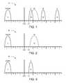
- FIG. 1illustrates a graphical diagram of voltage distributions which constitute different programming states of a programming model that may be used in conjunction with a MLC mode.
- FIG. 2illustrates a graphical diagram of programming states of one embodiment of a programming model which uses the LSB for the SLC mode.
- FIG. 3illustrates a graphical diagram of programming states of one embodiment of a programming model which uses the MSB for the SLC mode.
- FIG. 4illustrates a schematic block diagram of one embodiment of a network system.
- FIG. 5illustrates a flow chart diagram of one embodiment of a method for reading data from the storage device of FIG. 1 using conventional multi-phase read operations.
- FIG. 6illustrates a flow chart diagram of one embodiment of another method for reading data from the storage device of FIG. 1 using a single read operation.
- modulesare at least partially implemented in hardware, in one form or another.
- a modulemay be implemented as a hardware circuit comprising custom VLSI circuits or gate arrays, off-the-shelf semiconductors such as logic chips, transistors, or other discrete components.
- a modulemay also be implemented in programmable hardware devices such as field programmable gate arrays, programmable array logic, programmable logic devices or the like.
- Modulesmay also be implemented using software, stored on a physical storage device (e.g., a computer readable storage medium), for execution by various types of processors.
- a computer-readable storage mediuminclude, but are not limited to, a semiconductor or solid state memory, magnetic tape, a removable computer diskette, a random access memory (RAM), a read-only memory (ROM), a rigid magnetic disk, and an optical disk.
- Current examples of optical disksinclude a compact disk with read only memory (CD-ROM), a compact disk with read/write (CD-R/W), and a digital video disk (DVD).
- An identified module of executable codemay, for instance, comprise one or more physical or logical blocks of computer instructions which may, for instance, be organized as an object, procedure, or function. Nevertheless, the executables of an identified module need not be physically located together, but may comprise disparate instructions stored in different locations which, when joined logically together, comprise the module and achieve the stated purpose for the module.
- a module of executable codemay be a single instruction, or many instructions, and may even be distributed over several different code segments, among different programs, and across several storage or memory devices.
- operational datamay be identified and illustrated herein within modules, and may be embodied in any suitable form and organized within any suitable type of data structure. The operational data may be collected as a single data set, or may be distributed over different locations including over different storage devices, and may exist, at least partially, merely as electronic signals on a system or network.
- the software portionsare stored on one or more physical devices which are referred to herein as computer readable media.
- the software portionsare stored in a non-transitory state such that the software portions, or representations thereof, persist in the same physical location for a period of time. Additionally, in some embodiments the software portions are stored on one or more non-transitory storage devices, which include hardware elements capable of storing non-transitory states and/or signals representative of the software portions, even though other portions of the non-transitory storage devices may be capable of altering and/or transmitting the signals.
- a non-transitory storage deviceincludes a read-only memory (ROM) which can store signals and/or states representative of the software portions for a period of time.
- a processormay access the ROM to obtain signals that are representative of the stored signals and/or states in order to execute the corresponding software instructions.
- Reference to a computer readable mediummay take any physical form capable of storing machine-readable instructions, at least for a time in a non-transient state, on a digital processing apparatus.
- a computer readable mediummay be embodied by a compact disk, digital-video disk, a magnetic tape, a Bernoulli drive, a magnetic disk, flash memory, integrated circuits, or other digital processing apparatus memory device.
- embodiments of the inventionmay be combined in any suitable manner in one or more embodiments.
- numerous specific detailsare provided, such as examples of programming, software modules (stored on a physical device), user selections, network transactions, database queries, database structures, hardware modules, hardware circuits, hardware chips, etc., to provide a thorough understanding of embodiments of the invention.
- One skilled in the relevant artwill recognize, however, that embodiments of the invention may be practiced without one or more of the specific details, or with other methods, components, materials, and so forth.
- well-known structures, materials, or operationsare not shown or described in detail to avoid obscuring aspects of the invention.
- the schematic flow chart diagrams included hereinare generally set forth as logical flow chart diagrams. As such, the depicted order and labeled operations are indicative of one embodiment of the presented method. Other operations and methods may be conceived that are equivalent in function, logic, or effect to one or more operations, or portions thereof, of the illustrated method. Additionally, the format and symbols employed are provided to explain the logical operations of the method and are understood not to limit the scope of the method. Although various arrow types and line types may be employed in the flow chart diagrams, they are understood not to limit the scope of the corresponding method. Indeed, some arrows or other connectors may be used to indicate only the logical flow of the method. For instance, an arrow may indicate a waiting or monitoring period of unspecified duration between enumerated operations of the depicted method. Additionally, the order in which a particular method occurs may or may not strictly adhere to the order of the corresponding operations shown.
- the described embodimentsimplement a single-level cell (SLC) mode within a multi-level cell (MLC) memory device.
- the SLC moderestricts the number of programming states to which each MLC memory element may be programmed.
- the SLC moderestricts each MLC memory element to be programmed in either an erase state or a state which is closest to a natural threshold voltage of the MLC memory element.
- FIG. 1illustrates a graphical diagram 10 of various programming states of a programming model that may be used in conjunction with a MLC mode.
- Each programming stateincludes a range of voltages, which correspond to the horizontal axis. The vertical axis corresponds to zero volts. Voltages to the left are negative voltages, and voltages to the right are positive voltages. Other conventions may be used to designate the voltages.
- the natural threshold voltage, Vth(also designated as V th ), of the memory element is also identified.
- the natural threshold voltage of the memory elementrefers to a specific or approximate voltage level of the floating gate within the memory element.
- the natural threshold voltageis the voltage read from a newly manufactured memory element prior to executing an initial erase operation or write operation on the memory element. In this newly manufactured state there are no electrons on the floating gate of the memory element besides those that naturally exist in the floating gate material.
- the natural threshold voltageis about 0.5V and can range between about 0.1V and about 0.6V, although other embodiments may have a different natural threshold voltage.
- the natural threshold voltagegenerally correlates with a value approximately at which an inversion layer is formed in the substrate of the memory element. For example, if the natural threshold voltage is about 0.5V, then the inversion layer may be formed having a gate bias of at 0.6V or higher voltages.
- the programming statesinclude four designated programming states ERASE, A, B, and C (shown with solid lines) and one intermediate state (shown with dashed lines).
- the solid linesrepresent a statistical distribution of voltages for a set of cells of a given state once a programming operation is completed.
- Solid lines for ERASE, A, B, and C statesrepresent the possible states cells can take on when multiple bits of a MLC cell are programmed.
- the statistical distribution of voltages corresponding to the ERASE statespans from about ⁇ 2.25V to about ⁇ 1.5V.
- the statistical distribution of voltages corresponding to each of the other programming statesspan a range of about 0.5V-state A spans from about 0.5V to about 1.0V; state B spans from about 1.85V to about 2.35V; and state C spans from about 3.5V to about 4.0V.
- the spansmay be different and may start or end at different voltages.
- the intermediate statealso may be referred to as the low to middle (LM) state because it is between the state A and the state B.
- the intermediate LM statespans from about 0.7V to about 1.6V, although other embodiments may use other statistical distribution of voltages for the intermediate LM state.
- FIG. 1includes at least four designated programming states (ERASE, A, B, and C), each of which is operational to maintain a programming state corresponding to a value for a bit (or values for multiple bits) of data.
- an LM stateserves as a fifth designated programming state, for maintaining a programming state corresponding to one or more bit values.
- the designated programming states ERASE and A-Crepresent bit combinations 11 , 01 , 00 , and 10 (from the lowest voltage range to the highest voltage range).
- the left bitis the most significant bit (MSB)
- the right bitis the least significant bit (LSB).
- the intermediate stateis designated as 10 in the intermediate LM state to indicate that the LSB is set to zero, but the MSB is not yet set to a specific bit value.
- the designated programming state that represents the bit combination 11is also designated as the erase state.
- the MLC memory elementsare erased, by default each MLC memory element is returned to the erase state, which represents the bit combination 11 .
- the MLC memory elementis either left in the default erase state (to represent a logical 0) or programmed to the intermediate LM state (to represent a logical 1).
- the MSBmay be programmed. If the LSB is 1 and the MSB is supposed to be 1, then the MLC memory element is maintained in the erase state, because the erase state corresponds to the bit combination 11 . If the LSB is 1 and the MSB is supposed to be 0, then the MLC memory element is programmed to the state A corresponding to 01. If the LSB is programmed to 0, and the MSB is supposed to be 0, then the MLC memory element is programmed to the state B corresponding to 00. If the LSB is programmed to 0, and the MSB is supposed to be 1, then the MLC memory element is programmed to the state C corresponding to 10. This is just one example of bit combinations that may be assigned to the various programming states, according to a gray code programming model. Other embodiments may use other bit combinations assigned to the various programming states.
- the MLC memory elementis programmed in two or more phases. Programming the LSB is a first phase that places the MLC memory element in the erase state or the LM state. If all the pages of the MLC memory element are programmed using the multi-phase programming model, then certain cells may be programmed to transition from the LM state to either state B or state C, other cells may be programmed to transition from the erase state to state A, depending on the values that are programmed. This may be referred to as two-phase programming, because the programming is performed to the intermediate LM state in a first phase and then programmed to one of the states B or C in a second phase.
- the intermediate LM stateis used to program pages of the MLC memory element that use the LSB.
- Using an intermediate LM stateallows pages using the LSB to be programmed while pages that use the MSB are not programmed and allows the state of a cell to take one of the states Erase, A, B, or C when two or more pages that include the cell are programmed.
- states Erase, A, B, or Cwhen two or more pages that include the cell are programmed.
- pages for the MSB of the MLC memory elementare programmed then only states Erase and state A are used, as a result the intermediate LM state is not used.
- FIG. 2illustrates a graphical diagram 20 of programming states of one embodiment of a programming model which uses the LSB for the SLC mode.
- the value of the MSBmay be irrelevant.
- the MLC memory elementmay be programmed to the erase state to represent a bit value of 1, or to the intermediate LM state or either of the states B or C above (i.e., to the right of) the intermediate LM state to represent a bit value of 0. Since the programming model illustrated in FIG. 2 only uses a subset of the designated programming states for representing bit values, these programming states are referred to herein as “restricted programming states.” In general, restricted programming states include some, but not all, (i.e., an exclusive subset) of the designated programming states. In contrast, in this embodiment, the A, B, and C states of FIG. 1 are not used for any bit value representations, so the A, B and C states are not designated as restricted programming states.
- the restricted programming statescomprise states ERASE and C.
- the storage mediais a non-volatile storage media that does not have a natural threshold voltage such as a phase change memory and the like.
- use of states separated such as ERASE and Callow for more variation in the distribution of cells that are in each of the states.
- FIG. 3illustrates a graphical diagram 30 of programming states of one embodiment of a programming model which uses the MSB for the SLC mode.
- the value of the LSBremains 1.
- the MLC memory elementmay be programmed to the erase state to represent a bit value of 1 (a logical “0”), or to the state A to represent a bit value of 0 (a logical “1”).
- the state Arepresents the state that is closest to the threshold voltage Vth of the MLC memory element.
- the programming model illustrated in FIG. 3only uses a subset (i.e., ERASE and A states) of the designated programming states for representing bit values, these programming states are referred to herein as “restricted programming states.”
- the accuracy of the MLC deviceis maintained longer compared with using the MLC device in a MLC mode or using the MLC device in the SLC mode based on programming only pages that use the LSB. In this way, the longevity of the MLC device can be extended, because there is less programming voltage used to program the MLC memory elements to the lower voltage programming state.
- the MLC memory elementmight get overprogrammed relative to state A.
- the value of the MSBdoes not necessarily change between the states A and B, using the convention shown in FIG. 3 .
- this approach using the MSB state for the SLC modemay take about the same amount of time to program the MLC memory element than using only the LSB state. Reading from MLC memory element that have only the MSB state programmed may take a little longer since the MLC memory element may perform two or more reads to verify that the cell voltage is within the erase state or the A state. Additionally, this approach results in the creation of less electron trapping sites within the gate of the MLC memory elements due to the lower programming voltage applied, which contributes to the longevity of the MLC memory elements. In some embodiments, using the MSB only in NAND MLC reduces the amount of trapping charges due to program/erase (P/E) cycling by lowering the voltage swing.
- P/Eprogram/erase
- the number of electrons stored within a floating gateindicates a voltage differential that can be measured.
- the number of discrete levels that can be accurately determinedis dependent upon the total number of electrons that can be stored and the maximum variation in number of electrons that can be controlled.
- the crystalline or amorphous nature of the memory elementcan be determined, and the number of discrete levels that can be accurately determined depends on the number of intermediate states that can be implemented between the crystalline and amorphous states. While any number of levels may be implemented, regardless of the specific technology used to implement the MLC memory elements, many MLC memory elements have four levels representing two bits of information. The encoding of these levels to the bit values they represent may use a gray code or other encoding mechanisms.
- the two bits of a MLCwhile sharing the same physical memory cell, may not be contiguous in a logical address space. In many cases, the bits are in different pages. However, the lower order addresses for the bits are frequently the same. Also, the bits of a single memory element are typically (but not always) within the same erase blocks.
- An erase blockis a block of storage that is erased in bulk during an erase operation. The possible variations that might be implemented in different embodiments in terms of logical addresses, pages, erase blocks and so forth, may affect the operation of the device, but do not necessarily alter the fundamental concepts described herein for using a MLC device in a SLC mode.
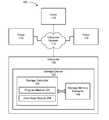
- FIG. 4illustrates a schematic block diagram of one embodiment of a network system 100 .
- the illustrated network system 100includes a storage device 102 with a storage controller 104 and storage memory elements 106 .
- the storage device 102is implemented within a computer 108 connected to one or more clients 110 through a computer network 112 .
- Embodiments of the depicted network system 100may be implemented to provide dedicated or shared storage resources for one or more of the clients 110 .
- Other embodiments of the network system 100may be implemented to provide storage resources or capacity in another manner.
- the storage memory elements 106may be implemented in any type of MLC technology capable of storing a signal or charge representative of multiple bits in a single storage location.
- the storage device 102includes MLC solid-state memory elements that are capable of operating in a SLC mode.
- solid-state memory elementscan be set to different programmable states that correspond to different bits or bit combinations.
- the storage device 102includes phase-change memory (PCM) elements that are capable of operating in a MLC mode or SLC mode.
- PCM elementscan be switched between multiple states, including a crystalline state, an amorphous, and one or more intermediate states.
- the storage device 102is internal to the computer 108 and is connected using a system bus, such as a peripheral component interconnect express (“PCI-e”) bus, a Serial Advanced Technology Attachment (“serial ATA”) bus, or the like.
- PCI-eperipheral component interconnect express
- serial ATASerial Advanced Technology Attachment
- the storage device 102is external to the computer 108 and is connected to a universal serial bus (“USB”) connection, an Institute of Electrical and Electronics Engineers (“IEEE”) 1394 bus (“FireWire”), or the like.
- IEEEInstitute of Electrical and Electronics Engineers
- the storage device 102is connected to the computer 108 using a peripheral component interconnect (“PCI”) express bus using an external electrical or optical bus extension or bus networking solution such as Infiniband or PCI Express Advanced Switching (“PCIe-AS”), or the like.
- Each storage device 102includes non-volatile, storage memory elements 106 , such as flash memory, nano random access memory (“nano RAM or NRAM”), magnetoresistive RAM (“MRAM”), dynamic RAM (“DRAM”), phase change RAM (“PRAM”), etc.
- NRAMnano random access memory
- MRAMmagnetoresistive RAM
- DRAMdynamic RAM
- PRAMphase change RAM
- the computer 108is shown with a single storage device 102 , other embodiments of the computer 108 may include more than one storage device 102 . Similarly, multiple storage devices 102 may be implemented at various locations within the nodes of the computer network 112 .
- the storage device 102may be in the form of a dual-inline memory module (“DIMM”), a daughter card, or a micro-module.
- DIMMdual-inline memory module
- the storage device 102is an element within a rack-mounted blade.
- the storage device 102is contained within a package that is integrated directly onto a higher level assembly (e.g., mother board, laptop, graphics processor, etc.).
- individual components including the storage device 102are integrated directly onto a higher level assembly without intermediate packaging.
- the illustrated computer 108is representative of one or more computers 108 coupled to each other and/or to the computer network 112 .
- the computer 108may be a host, a server, a storage controller of a storage area network (“SAN”), a workstation, a personal computer, a laptop computer, a handheld computer, a supercomputer, a computer cluster, a network switch, router, or appliance, a database or storage appliance, a data acquisition or data capture system, a diagnostic system, a test system, a robot, a portable electronic device, a wireless device, or the like.
- the computer 108may be a client (similar to the clients 110 ), and the storage device 102 operates autonomously to service data requests sent from the computer 108 .
- the computer 108 and storage device 102may be connected using the computer network 112 , system bus, or other communication means suitable for connection between a computer 108 and an autonomous storage device 102 .
- Each client 110may be a host, a server, a storage controller of a SAN, a workstation, a personal computer, a laptop computer, a handheld computer, a supercomputer, a computer cluster, a network switch, router, or appliance, a database or storage appliance, a data acquisition or data capture system, a diagnostic system, a test system, a robot, a portable electronic device, a wireless device, or the like.
- the computer network 112may include the Internet, a wide area network (“WAN”), a metropolitan area network (“MAN”), a local area network (“LAN”), a token ring, a wireless network, a fiber channel network, a SAN, network attached storage (“NAS”), ESCON, or the like, or any combination or portion(s) of networks.
- the computer network 112also may include a network from the IEEE 802 family of network technologies, such Ethernet, token ring, WiFi, WiMax, and the like.
- the computer network 112may include addition network nodes or components such as servers, switches, routers, cabling, radios, and other equipment used to facilitate the network connection between the computer 108 and the clients 110 .
- the network system 100includes multiple computers 108 that communicate as peers over the computer network 112 .
- the network system 100includes multiple storage devices 102 that communicate as peers over the computer network 112 .
- the storage controller 104provides functionality to utilize the storage memory elements 106 in a SLC mode.
- the storage controller 104may operate the storage memory elements 106 in either a MLC mode or a SLC mode.
- the storage controller 104may change between MLC and SLC operating modes for the storage memory elements 106 , depending on certain criteria. By operating the storage memory elements 106 in the SLC mode, certain operating benefits may be achieved including, for example, increased longevity of the storage device 102 .
- the illustrated storage controller 104includes a program module 202 and a data read module 204 .
- the program module 202programs one or more bits of a MLC memory element 106 of the storage device 102 .
- the program module 202programs the MLC memory element 106 in a SLC mode so that the MLC memory element 106 stores a single bit of data. While operating in the SLC mode, the program module 202 may program the MSB of each MLC memory element 106 . Regardless of the convention used to designate the MSB and LSB of each MLC memory element 106 , in some embodiments the program module 202 uses the bit that corresponds to the programming state closest to the natural threshold voltage of the MLC memory element 106 .
- the data read module 204reads at least one data bit within the MLC memory element 106 . If the storage device 102 is operating in the SLC mode, then the data read module 204 may read only a single bit from the MSB page of the MLC memory elements 106 . If the storage controller 104 uses the erase state and the programming state closest to the natural voltage threshold of the MLC memory element 106 , then the data read module 204 may read the MSB page once from each MLC memory element 106 .
- each MLC memory element 106is a cell that has 2 ⁇ X possible programming states, where X is equal to the number of bits per memory element 106 .
- a MLC memory element 106may store two bits of information and, accordingly, have four possible programming states.
- a MLC memory element 106may store three bits of information and, accordingly, have eight possible programming states.
- the MLC memory element 106 operating in SLC modestores at least a most significant bit (MSB).
- MSB and the LSBmay be assigned to different logical pages of the media.
- a plurality of the MLC memory elements 106is logically organized as a page on the storage device 102 .
- a pagemay be used as the designation of the smallest unit that can be written to the storage device 102 .
- the MLC memory element 106may be associated with a page pair.
- a page pairis a pair of pages (designated as upper and lower pages) that are associated with a single set of physical MLC memory elements 106 .
- Page pairsalso may be referred to as page tuples.
- a two-bit MLC memory element 106is associated with a page pair, in which the MSB is associated with an upper page and the LSB is associated with a lower page.
- the specific convention used to correlate the MSB/LSB with the upper/lower pages in a particular embodimentdoes not necessarily limit other conventions that may be used in other embodiments.
- the MSB and LSB in the same MLC memory element 106may have different logical addresses in the storage device 102 .
- writes directed to the upper page of the MLC memory element 106only change the MSB. This can be achieved by changing the programming state of the MLC memory element 106 from the erase state to the A state (See FIG. 3 ), in which case the value of the LSB is not changed.
- each stagemay include one or more incremental voltage level changes.
- changing the state of a MLC memory element 106 from the erase state to state Amay occur in a single programming phase over multiple incremental voltage level changes, each voltage level change increasing the voltage level of the MLC memory element 106 a fraction of the difference between the erase state and the A state.
- changing the state of a MLC memory element 106 from the erase state to the LM statemay be performed in a single programming phase over a single voltage level change (with a relatively high programming voltage) or over multiple incremental voltage level changes (each using a relatively low programming voltage).
- a clientsuch as a file system software application, operating system application, database management systems software application, a client computer, a client device, or the like
- a clientmay implement functionality to store data on the storage device 102 .
- the clientsends the write request with the data to be written, in one embodiment the data is written exclusively to the upper page corresponding to the MSBs of the MLC memory element 102 associated with that page.
- the MSBs in the various MLC memory elements 106are changed, but the LSBs are not changed.
- the write operationmay be implemented by following a page programming order defined by the manufacturer, but skipping the pages that correspond to the LSBs. In this way, the data can be written exclusively to the pages corresponding to the MSBs, while the pages corresponding to the LSBs are not used.
- read operationsmay be performed in one or more stages, depending on the available functionality of the storage device 102 .
- a first read operationis performed to determine if the state voltage of the MLC memory element 102 is between the ERASE state and the A state, and then a second read operation is performed to distinguish between the B and C states.
- a programming stateis identified, both the MSB and LSB may be known, because each programming state corresponds to two (or more) bits.
- itmay be sufficient to derive only the MSB, depending on which is used to designate the SLC value of the MLC memory element 106 .
- the data bitsare read in response to requests for data that has been stored on the storage device 102 . If the storage device 102 is operating in the SLC mode, then the read request is directed to the upper page such that the MSB is returned from the corresponding MLC memory elements 106 .
- writing data exclusively to the upper page corresponding to the MSBs of the MLC memory elements 106reduces the capacity of the storage device 102
- the reliability and/or longevity of the storage device 102is increased. More specifically, writing exclusively to the upper page may place less stress on the individual MLC memory elements 106 and, thereby, reduce instances of failure in the storage device 102 .
- the manufacturer and consumermay take advantage of the lower cost of the MLC storage media while getting performance comparable to, or better than, conventional SLC storage media.
- some embodimentsmay use mapping logic to handle mapping the pages, and a manufacturer may easily switch between MLC and SLC media for the storage device 102 , or different production runs, without having to make major redesigns each time.
- FIG. 5illustrates a flow chart diagram of one embodiment of a method 240 for reading data from the storage device 102 of FIG. 1 using conventional multi-phase read operations.
- This method 240corresponds to the programming model shown in FIG. 1 which uses both the LSB and the MSB.
- the method 240is described in conjunction with the storage device 102 of FIG. 1 , embodiments of the method 240 may be implemented with other types of storage devices 102 and/or programming models.
- the depicted method 240begins in response to the storage device 102 receiving 242 a read command.
- the read commandmay include address information to indicate the location of the data to be read.
- the storage device 102performs 244 a first read operation to determine the programmed state of the LSB. This operation is performed simply to determine if the LSB is programmed to the 0 state or 1 state.
- the storage device 102then performs 246 a second read operation to determine the programmed state of the MSB. If the MLC memory element 106 were operating in the MLC mode, then this read operation may be used to distinguish either between the erase state and the A state, or between the B state and the C state.
- the storage device 102then outputs 248 the value of the MSB, which represents the SLC value of the MLC memory element 106 .
- the depicted method 240then ends. Further embodiments of the depicted method 240 may include additional steps or operations which are equivalent in function and/or result.
- FIG. 6illustrates a flow chart diagram of one embodiment of another method 260 for reading data from the storage device 102 of FIG. 1 using a single read operation.
- a single read operationmay be possible if the manufacturer enables operation of MLC memory elements in a SLC mode that uses only the MSB pages, as described herein.
- the second read to distinguish between states B and Care not necessary because the LSB is not being utilized. Consequently, the MLC memory element may avoid the read latency by not performing this second read operation.
- the configuration of the MLC memory element to be operated in SLC mode using only the MSB state pagesmay be accomplished by default, in response to a command parameter, an initialization setting, or the like.
- This method 260corresponds to the programming model shown in FIG. 3 which uses the MSB for the SLC mode. Although the method 260 is described in conjunction with the storage device 102 of FIG. 1 and the programming model of FIG. 3 , embodiments of the method 260 may be implemented with other types of storage devices 102 and/or programming models.
- the depicted method 260begins in response to the storage device 102 receiving 262 a read command.
- the read commandmay include address information to indicate the location of the data to be read.
- the storage device 102performs 264 the read operation to determine the programmed state of the MSB. In this embodiment, there is no need to determine the programmed state of the LSB.
- the total read time of the read operationscan be reduced by about 60 microseconds relative to the read time of the multi-phase reading method 240 of FIG. 5 .
- the storage device 102may have built-in functionality that is capable of performing a read operation. However, in conventional storage devices 102 , this type of read functionality may only be available when the storage device is operated in a manufacturer proprietary configuration. In embodiments of the storage device 102 described herein, this read functionality can be accessed and executed while the storage device 102 is operating in a SLC storage mode. In some embodiments, the read functionality can be dynamically initiated in response to a determination that the MLC memory elements 106 are operating in the SLC mode. In other embodiments, a user may manually access and initiate the read functionality outside of the manufacturer proprietary configuration of the storage device 106 .
- the storage device 102then outputs 266 the value of the MSB, which represents the SLC value of the MLC memory element 106 .
- the depicted method 260then ends. Further embodiments of the depicted method 260 may include additional steps or operations which are equivalent in function and/or result.
- storing data in the MSBmay impact the overall functionality of the storage device 102 .
- the delay experienced in storing data in the MSBmay be decreased and the MLC memory elements 106 may exhibit less tendency to have values in the MSB inadvertently shift.
- storing the data in the MSBmay cause less wear on the MLC memory elements 106 for a particular programming operation. For example, referring to FIG. 3 , using the MSB to store data may involve only the erase state and the A state as valid states. Since the A state uses a lower programming voltage (compared with the B and C states), the MLC memory element 106 may experience less wear and/or damage as it is used.
- the storage device 102may dynamically reconfigure write and read requests to exclusively store data in the lower pages (LSB pages), or vice versa. In one embodiment, this is done by only programming the pages that correspond to the MSB pages, the LSB pages, or any middle bit pages, are simply skipped in the addressing of the pages. Alternatively, this is done by only programming the pages that correspond to the LSB pages, the MSB pages, or any middle bit pages, are simply skipped in the addressing of the pages.
- trigger eventswhich initiate the dynamic switch between different modes (e.g., MLC, SLC using the LSB, and SLC using the MSB).
- examples of some of the possible trigger eventsinclude, but are not necessarily limited to, an error count for MLC memory elements satisfying a threshold, P/E cycle count satisfying a threshold, and/or a change in storage capacity requirements (e.g., a need for more storage might trigger a switch from an SLC mode to the MLC mode).
- a combination of trigger eventsmay be used to initiate the dynamic switch between modes.
- one or more other trigger events that are identifiable by one skilled in the art in light of the embodiments described hereinmay be used.
- An embodiment of the storage device 102includes at least one hardware-implemented processing device coupled directly or indirectly to memory elements through a system bus such as a data, address, and/or control bus.
- the memory elementscan include local memory employed during actual execution of the program code, bulk storage, and cache memories which provide temporary storage of at least some program code in order to reduce the number of times code must be retrieved from bulk storage during execution.
Landscapes
- Engineering & Computer Science (AREA)
- Computer Hardware Design (AREA)
- Microelectronics & Electronic Packaging (AREA)
- Read Only Memory (AREA)
Abstract
Description
- This application is a continuation-in-part of U.S. application Ser. No. 12/724,401 (U.S. Pat. Pub. No. 20100235715), entitled “Apparatus, System, and Method for Using Multi-Level Cell Solid-State Storage as Single-Level Cell Solid-State Storage,” filed on Mar. 15, 2010, which claims the benefit of U.S. Provisional Patent Application No. 61/160,258, entitled “Apparatus, System, and Method for Using Multi-Level Cell Solid-State Storage as Single-Level Cell Solid-State Storage,” filed on Mar. 13, 2009, both of which are incorporated by reference herein.
- Some conventional flash memory and other solid-state storage devices implement multi-level cell (MLC) memory elements to store multiple bits of data in the same memory cell. In general, the MLC memory elements are programmable to multiple states, which are each characterized by separate voltage thresholds. As an example, a two-bit MLC memory element can be programmed to one of four different states, each state corresponding to a unique voltage range.
- Storing multiple bits of data in the same memory element increases the capacity of the flash memory. However, this approach also typically decreases the longevity of the device in various ways, including the number of times each memory element can be accurately written, the number of times each memory element can be accurately read per write, and the ability to maintain the accuracy of the data, for example, when the flash memory is not powered, is operating at high temperatures, or under other conditions. While the availability of increased capacity may drive the use of MLC memory element in flash memory, the possibility of decreased accuracy or product life can be a deterrent. By way of comparison, single-level cell (SLC) memory elements may have better accuracy and/or longer life, but are typically more expensive to manufacture (i.e., greater cost per bit).
- As a compromise between MLC and SLC memory elements, some flash memory and other solid-state storage devices implement an SLC mode using MLC memory elements. In this mode, each MLC memory element is used to store a single bit, rather than multiple bits. This approach may provide improved accuracy and/or longevity compared with conventional MLC memory devices, while maintaining a lower cost per bit than conventional SLC memory devices.
- Embodiments of a method are described. In one embodiment, the method is a method for storing data in an electronic memory device. An embodiment of the method includes receiving a write command to write data to an electronic memory device having multi-level cell (MLC) memory elements. Each MLC memory element is programmable to designated programming states. Each designated programming state is representative of at least two bits of data. An embodiment of the method also includes programming at least one of the MLC memory elements to one of a plurality of restricted programming states in a single-level cell (SLC) mode to represent at most a single bit of data at each of the restricted programming states. The restricted programming states exclude at least one of the designated programming states. The restricted programming states include a first state which is an erase state. The restricted programming states also include at least a second state, other than the erase state, which is closest to a natural threshold voltage of the MLC memory elements. Other embodiments of the method are also described.
- Embodiments of a computer program product are also described. In one embodiment, the computer program product includes a computer readable storage device to store a computer readable program, wherein the computer readable program, when executed by a processor within a computer, causes the computer to perform operations for storing data in an electronic memory device. The operations include receiving a write command to write the data to an electronic memory device having multi-level cell (MLC) memory elements. Each MLC memory element is programmable to 2̂X designated programming states. Each designated programming state is representative of X bits of data, where X>1. The operations also include programming at least one of the MLC memory elements to one of a plurality of restricted programming states in a reduced-level cell (RLC) mode to represent Y bits of the data, where Y<X. The restricted programming states exclude at least one of the designated programming states. The restricted programming states include a first state which is an erase state. The restricted programming states also include a second state, other than the erase state, which is closest to a natural threshold voltage of the MLC memory elements. Other embodiments of the computer programming product are also described.
- Embodiments of an apparatus are also described. In one embodiment, the apparatus is a controller for an electronic memory device having multi-level cell (MLC) memory elements. Each MLC memory element is capable of storing at least two bits. An embodiment of the controller includes a physical interface to couple the controller to the electronic memory device. The controller also includes a processing unit coupled to the physical interface. The processing unit operates the electronic memory device in a single-level cell (SLC) mode using a restricted number of programming states for a single data bit. The restricted number of programming states includes a first state which is an erase state. The restricted number of programming states also includes a second state, other than the erase state, which is closest to a natural threshold voltage of the MLC memory elements. Other embodiments of the apparatus are also described.
- Other aspects and advantages of embodiments of the present invention will become apparent from the following detailed description, taken in conjunction with the accompanying drawings, illustrated by way of example of the principles of the invention.
FIG. 1 illustrates a graphical diagram of voltage distributions which constitute different programming states of a programming model that may be used in conjunction with a MLC mode.FIG. 2 illustrates a graphical diagram of programming states of one embodiment of a programming model which uses the LSB for the SLC mode.FIG. 3 illustrates a graphical diagram of programming states of one embodiment of a programming model which uses the MSB for the SLC mode.FIG. 4 illustrates a schematic block diagram of one embodiment of a network system.FIG. 5 illustrates a flow chart diagram of one embodiment of a method for reading data from the storage device ofFIG. 1 using conventional multi-phase read operations.FIG. 6 illustrates a flow chart diagram of one embodiment of another method for reading data from the storage device ofFIG. 1 using a single read operation.- Throughout the description, similar reference numbers may be used to identify similar elements.
- Many of the functional units described in this specification have been labeled as modules, in order to more particularly emphasize their implementation independence. Modules are at least partially implemented in hardware, in one form or another. For example, a module may be implemented as a hardware circuit comprising custom VLSI circuits or gate arrays, off-the-shelf semiconductors such as logic chips, transistors, or other discrete components. A module may also be implemented in programmable hardware devices such as field programmable gate arrays, programmable array logic, programmable logic devices or the like.
- Modules may also be implemented using software, stored on a physical storage device (e.g., a computer readable storage medium), for execution by various types of processors. Examples of a computer-readable storage medium include, but are not limited to, a semiconductor or solid state memory, magnetic tape, a removable computer diskette, a random access memory (RAM), a read-only memory (ROM), a rigid magnetic disk, and an optical disk. Current examples of optical disks include a compact disk with read only memory (CD-ROM), a compact disk with read/write (CD-R/W), and a digital video disk (DVD).
- An identified module of executable code may, for instance, comprise one or more physical or logical blocks of computer instructions which may, for instance, be organized as an object, procedure, or function. Nevertheless, the executables of an identified module need not be physically located together, but may comprise disparate instructions stored in different locations which, when joined logically together, comprise the module and achieve the stated purpose for the module.
- Indeed, a module of executable code may be a single instruction, or many instructions, and may even be distributed over several different code segments, among different programs, and across several storage or memory devices. Similarly, operational data may be identified and illustrated herein within modules, and may be embodied in any suitable form and organized within any suitable type of data structure. The operational data may be collected as a single data set, or may be distributed over different locations including over different storage devices, and may exist, at least partially, merely as electronic signals on a system or network. Where a module or portions of a module are implemented in software, the software portions are stored on one or more physical devices which are referred to herein as computer readable media.
- In some embodiments, the software portions are stored in a non-transitory state such that the software portions, or representations thereof, persist in the same physical location for a period of time. Additionally, in some embodiments the software portions are stored on one or more non-transitory storage devices, which include hardware elements capable of storing non-transitory states and/or signals representative of the software portions, even though other portions of the non-transitory storage devices may be capable of altering and/or transmitting the signals. One example of a non-transitory storage device includes a read-only memory (ROM) which can store signals and/or states representative of the software portions for a period of time. However, the ability to store the signals and/or states is not diminished by further functionality of transmitting signals that are the same as or representative of the stored signals and/or states. For example, a processor may access the ROM to obtain signals that are representative of the stored signals and/or states in order to execute the corresponding software instructions.
- Reference throughout this specification to “one embodiment,” “an embodiment,” or similar language means that a particular feature, structure, or characteristic described in connection with the embodiment is included in at least one embodiment of the present invention. Thus, appearances of the phrases “in one embodiment,” “in an embodiment,” and similar language throughout this specification may, but do not necessarily, all refer to the same embodiment.
- Reference to a computer readable medium may take any physical form capable of storing machine-readable instructions, at least for a time in a non-transient state, on a digital processing apparatus. A computer readable medium may be embodied by a compact disk, digital-video disk, a magnetic tape, a Bernoulli drive, a magnetic disk, flash memory, integrated circuits, or other digital processing apparatus memory device.
- Furthermore, the described features, structures, or characteristics of embodiments of the invention may be combined in any suitable manner in one or more embodiments. In the following description, numerous specific details are provided, such as examples of programming, software modules (stored on a physical device), user selections, network transactions, database queries, database structures, hardware modules, hardware circuits, hardware chips, etc., to provide a thorough understanding of embodiments of the invention. One skilled in the relevant art will recognize, however, that embodiments of the invention may be practiced without one or more of the specific details, or with other methods, components, materials, and so forth. In other instances, well-known structures, materials, or operations are not shown or described in detail to avoid obscuring aspects of the invention.
- The schematic flow chart diagrams included herein are generally set forth as logical flow chart diagrams. As such, the depicted order and labeled operations are indicative of one embodiment of the presented method. Other operations and methods may be conceived that are equivalent in function, logic, or effect to one or more operations, or portions thereof, of the illustrated method. Additionally, the format and symbols employed are provided to explain the logical operations of the method and are understood not to limit the scope of the method. Although various arrow types and line types may be employed in the flow chart diagrams, they are understood not to limit the scope of the corresponding method. Indeed, some arrows or other connectors may be used to indicate only the logical flow of the method. For instance, an arrow may indicate a waiting or monitoring period of unspecified duration between enumerated operations of the depicted method. Additionally, the order in which a particular method occurs may or may not strictly adhere to the order of the corresponding operations shown.
- While many embodiments are described herein, at least some of the described embodiments implement a single-level cell (SLC) mode within a multi-level cell (MLC) memory device. The SLC mode restricts the number of programming states to which each MLC memory element may be programmed. In a specific embodiment, the SLC mode restricts each MLC memory element to be programmed in either an erase state or a state which is closest to a natural threshold voltage of the MLC memory element.
FIG. 1 illustrates a graphical diagram10 of various programming states of a programming model that may be used in conjunction with a MLC mode. Each programming state includes a range of voltages, which correspond to the horizontal axis. The vertical axis corresponds to zero volts. Voltages to the left are negative voltages, and voltages to the right are positive voltages. Other conventions may be used to designate the voltages.- The natural threshold voltage, Vth (also designated as Vth), of the memory element is also identified. The natural threshold voltage of the memory element refers to a specific or approximate voltage level of the floating gate within the memory element. The natural threshold voltage is the voltage read from a newly manufactured memory element prior to executing an initial erase operation or write operation on the memory element. In this newly manufactured state there are no electrons on the floating gate of the memory element besides those that naturally exist in the floating gate material. In some embodiments, the natural threshold voltage is about 0.5V and can range between about 0.1V and about 0.6V, although other embodiments may have a different natural threshold voltage. The natural threshold voltage generally correlates with a value approximately at which an inversion layer is formed in the substrate of the memory element. For example, if the natural threshold voltage is about 0.5V, then the inversion layer may be formed having a gate bias of at 0.6V or higher voltages.
- The programming states include four designated programming states ERASE, A, B, and C (shown with solid lines) and one intermediate state (shown with dashed lines). The solid lines represent a statistical distribution of voltages for a set of cells of a given state once a programming operation is completed. Solid lines for ERASE, A, B, and C states represent the possible states cells can take on when multiple bits of a MLC cell are programmed. In the illustrated example, the statistical distribution of voltages corresponding to the ERASE state spans from about −2.25V to about −1.5V. The statistical distribution of voltages corresponding to each of the other programming states span a range of about 0.5V-state A spans from about 0.5V to about 1.0V; state B spans from about 1.85V to about 2.35V; and state C spans from about 3.5V to about 4.0V. In other embodiments, the spans may be different and may start or end at different voltages.
- The intermediate state also may be referred to as the low to middle (LM) state because it is between the state A and the state B. In the illustrated embodiment, the intermediate LM state spans from about 0.7V to about 1.6V, although other embodiments may use other statistical distribution of voltages for the intermediate LM state.
- The term “designated programming states” is used herein to refer to the group of all states which are available for programming based on a manufacturer's design and implementation. For example,
FIG. 1 includes at least four designated programming states (ERASE, A, B, and C), each of which is operational to maintain a programming state corresponding to a value for a bit (or values for multiple bits) of data. In some embodiments, an LM state serves as a fifth designated programming state, for maintaining a programming state corresponding to one or more bit values. - In the illustrated embodiment, the designated programming states ERASE and A-C represent
bit combinations - In operation, the designated programming state that represents the
bit combination 11 is also designated as the erase state. When the MLC memory elements are erased, by default each MLC memory element is returned to the erase state, which represents thebit combination 11. In order to program the MLC memory element, the MLC memory element is either left in the default erase state (to represent a logical 0) or programmed to the intermediate LM state (to represent a logical 1). - Once the LSB is programmed, then the MSB may be programmed. If the LSB is 1 and the MSB is supposed to be 1, then the MLC memory element is maintained in the erase state, because the erase state corresponds to the
bit combination 11. If the LSB is 1 and the MSB is supposed to be 0, then the MLC memory element is programmed to the state A corresponding to 01. If the LSB is programmed to 0, and the MSB is supposed to be 0, then the MLC memory element is programmed to the state B corresponding to 00. If the LSB is programmed to 0, and the MSB is supposed to be 1, then the MLC memory element is programmed to the state C corresponding to 10. This is just one example of bit combinations that may be assigned to the various programming states, according to a gray code programming model. Other embodiments may use other bit combinations assigned to the various programming states. - The MLC memory element is programmed in two or more phases. Programming the LSB is a first phase that places the MLC memory element in the erase state or the LM state. If all the pages of the MLC memory element are programmed using the multi-phase programming model, then certain cells may be programmed to transition from the LM state to either state B or state C, other cells may be programmed to transition from the erase state to state A, depending on the values that are programmed. This may be referred to as two-phase programming, because the programming is performed to the intermediate LM state in a first phase and then programmed to one of the states B or C in a second phase.
- The intermediate LM state is used to program pages of the MLC memory element that use the LSB. Using an intermediate LM state allows pages using the LSB to be programmed while pages that use the MSB are not programmed and allows the state of a cell to take one of the states Erase, A, B, or C when two or more pages that include the cell are programmed. In contrast, if pages for the MSB of the MLC memory element are programmed then only states Erase and state A are used, as a result the intermediate LM state is not used.
FIG. 2 illustrates a graphical diagram20 of programming states of one embodiment of a programming model which uses the LSB for the SLC mode. In this programming model, the value of the MSB may be irrelevant. The MLC memory element may be programmed to the erase state to represent a bit value of 1, or to the intermediate LM state or either of the states B or C above (i.e., to the right of) the intermediate LM state to represent a bit value of 0. Since the programming model illustrated inFIG. 2 only uses a subset of the designated programming states for representing bit values, these programming states are referred to herein as “restricted programming states.” In general, restricted programming states include some, but not all, (i.e., an exclusive subset) of the designated programming states. In contrast, in this embodiment, the A, B, and C states ofFIG. 1 are not used for any bit value representations, so the A, B and C states are not designated as restricted programming states.- Referring back to
FIG. 1 , in one embodiment, the restricted programming states comprise states ERASE and C. Such an embodiment may be advantageous where the storage media is a non-volatile storage media that does not have a natural threshold voltage such as a phase change memory and the like. In such an embodiment, use of states separated such as ERASE and C allow for more variation in the distribution of cells that are in each of the states. FIG. 3 illustrates a graphical diagram30 of programming states of one embodiment of a programming model which uses the MSB for the SLC mode. In this programming model, the value of the LSB remains 1. The MLC memory element may be programmed to the erase state to represent a bit value of 1 (a logical “0”), or to the state A to represent a bit value of 0 (a logical “1”). For reference, the state A represents the state that is closest to the threshold voltage Vth of the MLC memory element. Also, since the programming model illustrated inFIG. 3 only uses a subset (i.e., ERASE and A states) of the designated programming states for representing bit values, these programming states are referred to herein as “restricted programming states.”- In some embodiments, by utilizing the state that is closest to the threshold voltage Vth of the MLC memory element for the SLC mode, the accuracy of the MLC device is maintained longer compared with using the MLC device in a MLC mode or using the MLC device in the SLC mode based on programming only pages that use the LSB. In this way, the longevity of the MLC device can be extended, because there is less programming voltage used to program the MLC memory elements to the lower voltage programming state.
- Additionally, in some embodiments it is relatively unlikely that the MLC memory element might get overprogrammed relative to state A. In fact, even if the MLC memory element is overprogrammed relative to state A, the value of the MSB does not necessarily change between the states A and B, using the convention shown in
FIG. 3 . - Also, in certain embodiments, this approach using the MSB state for the SLC mode may take about the same amount of time to program the MLC memory element than using only the LSB state. Reading from MLC memory element that have only the MSB state programmed may take a little longer since the MLC memory element may perform two or more reads to verify that the cell voltage is within the erase state or the A state. Additionally, this approach results in the creation of less electron trapping sites within the gate of the MLC memory elements due to the lower programming voltage applied, which contributes to the longevity of the MLC memory elements. In some embodiments, using the MSB only in NAND MLC reduces the amount of trapping charges due to program/erase (P/E) cycling by lowering the voltage swing. If there are less trapped charges and/or trap sites, then there is low trap-assisted tunneling and path through a string of traps. Consequently, this also makes it less likely that the MLC memory element might be overprogrammed relative to state A. Moreover, there is very little voltage (Vt) drift of state A because the Vt level of state A is relatively close to the natural Vt level of the MLC memory element. This possibility of overprogramming typically increases with the age of the MLC device.
- Typically in a MLC flash memory element, the number of electrons stored within a floating gate indicates a voltage differential that can be measured. The number of discrete levels that can be accurately determined is dependent upon the total number of electrons that can be stored and the maximum variation in number of electrons that can be controlled. Similarly, in a MLC phase-change memory element, the crystalline or amorphous nature of the memory element can be determined, and the number of discrete levels that can be accurately determined depends on the number of intermediate states that can be implemented between the crystalline and amorphous states. While any number of levels may be implemented, regardless of the specific technology used to implement the MLC memory elements, many MLC memory elements have four levels representing two bits of information. The encoding of these levels to the bit values they represent may use a gray code or other encoding mechanisms.
- The two bits of a MLC, while sharing the same physical memory cell, may not be contiguous in a logical address space. In many cases, the bits are in different pages. However, the lower order addresses for the bits are frequently the same. Also, the bits of a single memory element are typically (but not always) within the same erase blocks. An erase block is a block of storage that is erased in bulk during an erase operation. The possible variations that might be implemented in different embodiments in terms of logical addresses, pages, erase blocks and so forth, may affect the operation of the device, but do not necessarily alter the fundamental concepts described herein for using a MLC device in a SLC mode.
FIG. 4 illustrates a schematic block diagram of one embodiment of anetwork system 100. The illustratednetwork system 100 includes astorage device 102 with astorage controller 104 andstorage memory elements 106. Thestorage device 102 is implemented within acomputer 108 connected to one ormore clients 110 through acomputer network 112. Embodiments of the depictednetwork system 100 may be implemented to provide dedicated or shared storage resources for one or more of theclients 110. Other embodiments of thenetwork system 100 may be implemented to provide storage resources or capacity in another manner.- The
storage memory elements 106 may be implemented in any type of MLC technology capable of storing a signal or charge representative of multiple bits in a single storage location. In one embodiment, thestorage device 102 includes MLC solid-state memory elements that are capable of operating in a SLC mode. In general, solid-state memory elements can be set to different programmable states that correspond to different bits or bit combinations. In another embodiment, thestorage device 102 includes phase-change memory (PCM) elements that are capable of operating in a MLC mode or SLC mode. In general, PCM elements can be switched between multiple states, including a crystalline state, an amorphous, and one or more intermediate states. - In one embodiment, the
storage device 102 is internal to thecomputer 108 and is connected using a system bus, such as a peripheral component interconnect express (“PCI-e”) bus, a Serial Advanced Technology Attachment (“serial ATA”) bus, or the like. In another embodiment, thestorage device 102 is external to thecomputer 108 and is connected to a universal serial bus (“USB”) connection, an Institute of Electrical and Electronics Engineers (“IEEE”)1394 bus (“FireWire”), or the like. In other embodiments, thestorage device 102 is connected to thecomputer 108 using a peripheral component interconnect (“PCI”) express bus using an external electrical or optical bus extension or bus networking solution such as Infiniband or PCI Express Advanced Switching (“PCIe-AS”), or the like. - Each
storage device 102 includes non-volatile,storage memory elements 106, such as flash memory, nano random access memory (“nano RAM or NRAM”), magnetoresistive RAM (“MRAM”), dynamic RAM (“DRAM”), phase change RAM (“PRAM”), etc. Although thecomputer 108 is shown with asingle storage device 102, other embodiments of thecomputer 108 may include more than onestorage device 102. Similarly,multiple storage devices 102 may be implemented at various locations within the nodes of thecomputer network 112. - In various embodiments, the
storage device 102 may be in the form of a dual-inline memory module (“DIMM”), a daughter card, or a micro-module. In another embodiment, thestorage device 102 is an element within a rack-mounted blade. In another embodiment, thestorage device 102 is contained within a package that is integrated directly onto a higher level assembly (e.g., mother board, laptop, graphics processor, etc.). In another embodiment, individual components including thestorage device 102 are integrated directly onto a higher level assembly without intermediate packaging. - The illustrated
computer 108 is representative of one ormore computers 108 coupled to each other and/or to thecomputer network 112. Thecomputer 108 may be a host, a server, a storage controller of a storage area network (“SAN”), a workstation, a personal computer, a laptop computer, a handheld computer, a supercomputer, a computer cluster, a network switch, router, or appliance, a database or storage appliance, a data acquisition or data capture system, a diagnostic system, a test system, a robot, a portable electronic device, a wireless device, or the like. In another embodiment, thecomputer 108 may be a client (similar to the clients110), and thestorage device 102 operates autonomously to service data requests sent from thecomputer 108. In this embodiment, thecomputer 108 andstorage device 102 may be connected using thecomputer network 112, system bus, or other communication means suitable for connection between acomputer 108 and anautonomous storage device 102. - Each
client 110 may be a host, a server, a storage controller of a SAN, a workstation, a personal computer, a laptop computer, a handheld computer, a supercomputer, a computer cluster, a network switch, router, or appliance, a database or storage appliance, a data acquisition or data capture system, a diagnostic system, a test system, a robot, a portable electronic device, a wireless device, or the like. - The
computer network 112 may include the Internet, a wide area network (“WAN”), a metropolitan area network (“MAN”), a local area network (“LAN”), a token ring, a wireless network, a fiber channel network, a SAN, network attached storage (“NAS”), ESCON, or the like, or any combination or portion(s) of networks. Thecomputer network 112 also may include a network from the IEEE 802 family of network technologies, such Ethernet, token ring, WiFi, WiMax, and the like. - The
computer network 112 may include addition network nodes or components such as servers, switches, routers, cabling, radios, and other equipment used to facilitate the network connection between thecomputer 108 and theclients 110. In one embodiment, thenetwork system 100 includesmultiple computers 108 that communicate as peers over thecomputer network 112. In another embodiment, thenetwork system 100 includesmultiple storage devices 102 that communicate as peers over thecomputer network 112. - For a
storage device 102 that is designed to operate in a MLC mode, thestorage controller 104 provides functionality to utilize thestorage memory elements 106 in a SLC mode. In some embodiments, thestorage controller 104 may operate thestorage memory elements 106 in either a MLC mode or a SLC mode. Alternatively, thestorage controller 104 may change between MLC and SLC operating modes for thestorage memory elements 106, depending on certain criteria. By operating thestorage memory elements 106 in the SLC mode, certain operating benefits may be achieved including, for example, increased longevity of thestorage device 102. - The illustrated
storage controller 104 includes aprogram module 202 and a data readmodule 204. In one embodiment, theprogram module 202 programs one or more bits of aMLC memory element 106 of thestorage device 102. In certain embodiments, theprogram module 202 programs theMLC memory element 106 in a SLC mode so that theMLC memory element 106 stores a single bit of data. While operating in the SLC mode, theprogram module 202 may program the MSB of eachMLC memory element 106. Regardless of the convention used to designate the MSB and LSB of eachMLC memory element 106, in some embodiments theprogram module 202 uses the bit that corresponds to the programming state closest to the natural threshold voltage of theMLC memory element 106. - In one embodiment, the data read
module 204 reads at least one data bit within theMLC memory element 106. If thestorage device 102 is operating in the SLC mode, then the data readmodule 204 may read only a single bit from the MSB page of theMLC memory elements 106. If thestorage controller 104 uses the erase state and the programming state closest to the natural voltage threshold of theMLC memory element 106, then the data readmodule 204 may read the MSB page once from eachMLC memory element 106. - In some embodiments, each
MLC memory element 106 is a cell that has 2̂X possible programming states, where X is equal to the number of bits permemory element 106. For example, aMLC memory element 106 may store two bits of information and, accordingly, have four possible programming states. As another example, aMLC memory element 106 may store three bits of information and, accordingly, have eight possible programming states. - The
MLC memory element 106 operating in SLC mode stores at least a most significant bit (MSB). In certain embodiments, even though the MSB and the LSB are part of the same physical multi-level memory cell402, the MSB and the LSB may be assigned to different logical pages of the media. In certain embodiments, a plurality of theMLC memory elements 106 is logically organized as a page on thestorage device 102. A page may be used as the designation of the smallest unit that can be written to thestorage device 102. Moreover, theMLC memory element 106 may be associated with a page pair. A page pair is a pair of pages (designated as upper and lower pages) that are associated with a single set of physicalMLC memory elements 106. Page pairs also may be referred to as page tuples. In one example, a two-bitMLC memory element 106 is associated with a page pair, in which the MSB is associated with an upper page and the LSB is associated with a lower page. The specific convention used to correlate the MSB/LSB with the upper/lower pages in a particular embodiment does not necessarily limit other conventions that may be used in other embodiments. Thus, the MSB and LSB in the sameMLC memory element 106 may have different logical addresses in thestorage device 102. - In one embodiment, writes directed to the upper page of the
MLC memory element 106 only change the MSB. This can be achieved by changing the programming state of theMLC memory element 106 from the erase state to the A state (SeeFIG. 3 ), in which case the value of the LSB is not changed. - Additionally, the write operations may be implemented in one or more stages, and each stage may include one or more incremental voltage level changes. For example, changing the state of a
MLC memory element 106 from the erase state to state A may occur in a single programming phase over multiple incremental voltage level changes, each voltage level change increasing the voltage level of the MLC memory element106 a fraction of the difference between the erase state and the A state. In another example, changing the state of aMLC memory element 106 from the erase state to the LM state may be performed in a single programming phase over a single voltage level change (with a relatively high programming voltage) or over multiple incremental voltage level changes (each using a relatively low programming voltage). - As one example of a write operation, a client (such as a file system software application, operating system application, database management systems software application, a client computer, a client device, or the like) may implement functionality to store data on the
storage device 102. When the client sends the write request with the data to be written, in one embodiment the data is written exclusively to the upper page corresponding to the MSBs of theMLC memory element 102 associated with that page. As a result of the write operation, the MSBs in the variousMLC memory elements 106 are changed, but the LSBs are not changed. Although there may be various ways to write data exclusively to one page or the other, in one embodiment the write operation may be implemented by following a page programming order defined by the manufacturer, but skipping the pages that correspond to the LSBs. In this way, the data can be written exclusively to the pages corresponding to the MSBs, while the pages corresponding to the LSBs are not used. - Similar to write operations, read operations may be performed in one or more stages, depending on the available functionality of the
storage device 102. In some embodiments, a first read operation is performed to determine if the state voltage of theMLC memory element 102 is between the ERASE state and the A state, and then a second read operation is performed to distinguish between the B and C states. Once a programming state is identified, both the MSB and LSB may be known, because each programming state corresponds to two (or more) bits. However, when using aMLC memory element 106 in the SLC mode, it may be sufficient to derive only the MSB, depending on which is used to designate the SLC value of theMLC memory element 106. - In certain embodiments, the data bits are read in response to requests for data that has been stored on the
storage device 102. If thestorage device 102 is operating in the SLC mode, then the read request is directed to the upper page such that the MSB is returned from the correspondingMLC memory elements 106. - Although writing data exclusively to the upper page corresponding to the MSBs of the
MLC memory elements 106 reduces the capacity of thestorage device 102, in some embodiments the reliability and/or longevity of thestorage device 102 is increased. More specifically, writing exclusively to the upper page may place less stress on the individualMLC memory elements 106 and, thereby, reduce instances of failure in thestorage device 102. In addition, the manufacturer and consumer may take advantage of the lower cost of the MLC storage media while getting performance comparable to, or better than, conventional SLC storage media. Furthermore, some embodiments may use mapping logic to handle mapping the pages, and a manufacturer may easily switch between MLC and SLC media for thestorage device 102, or different production runs, without having to make major redesigns each time. FIG. 5 illustrates a flow chart diagram of one embodiment of amethod 240 for reading data from thestorage device 102 ofFIG. 1 using conventional multi-phase read operations. Thismethod 240 corresponds to the programming model shown inFIG. 1 which uses both the LSB and the MSB. Although themethod 240 is described in conjunction with thestorage device 102 ofFIG. 1 , embodiments of themethod 240 may be implemented with other types ofstorage devices 102 and/or programming models.- The depicted
method 240 begins in response to thestorage device 102 receiving242 a read command. The read command may include address information to indicate the location of the data to be read. - In response to the read command, the
storage device 102 performs244 a first read operation to determine the programmed state of the LSB. This operation is performed simply to determine if the LSB is programmed to the 0 state or 1 state. - The
storage device 102 then performs246 a second read operation to determine the programmed state of the MSB. If theMLC memory element 106 were operating in the MLC mode, then this read operation may be used to distinguish either between the erase state and the A state, or between the B state and the C state. Thestorage device 102 then outputs248 the value of the MSB, which represents the SLC value of theMLC memory element 106. The depictedmethod 240 then ends. Further embodiments of the depictedmethod 240 may include additional steps or operations which are equivalent in function and/or result. - In contrast to the multi-phase approach shown in
FIG. 5 ,FIG. 6 illustrates a flow chart diagram of one embodiment of anothermethod 260 for reading data from thestorage device 102 ofFIG. 1 using a single read operation. Such a single read operation may be possible if the manufacturer enables operation of MLC memory elements in a SLC mode that uses only the MSB pages, as described herein. Under such use conditions, the second read to distinguish between states B and C are not necessary because the LSB is not being utilized. Consequently, the MLC memory element may avoid the read latency by not performing this second read operation. The configuration of the MLC memory element to be operated in SLC mode using only the MSB state pages may be accomplished by default, in response to a command parameter, an initialization setting, or the like. Thismethod 260 corresponds to the programming model shown inFIG. 3 which uses the MSB for the SLC mode. Although themethod 260 is described in conjunction with thestorage device 102 ofFIG. 1 and the programming model ofFIG. 3 , embodiments of themethod 260 may be implemented with other types ofstorage devices 102 and/or programming models. - The depicted
method 260 begins in response to thestorage device 102 receiving262 a read command. The read command may include address information to indicate the location of the data to be read. - In response to the read command, the
storage device 102 performs264 the read operation to determine the programmed state of the MSB. In this embodiment, there is no need to determine the programmed state of the LSB. By performing only a single read operation, instead of multiple read operations, the total read time of the read operations can be reduced by about 60 microseconds relative to the read time of themulti-phase reading method 240 ofFIG. 5 . - In some embodiments, the
storage device 102 may have built-in functionality that is capable of performing a read operation. However, inconventional storage devices 102, this type of read functionality may only be available when the storage device is operated in a manufacturer proprietary configuration. In embodiments of thestorage device 102 described herein, this read functionality can be accessed and executed while thestorage device 102 is operating in a SLC storage mode. In some embodiments, the read functionality can be dynamically initiated in response to a determination that theMLC memory elements 106 are operating in the SLC mode. In other embodiments, a user may manually access and initiate the read functionality outside of the manufacturer proprietary configuration of thestorage device 106. - The
storage device 102 then outputs266 the value of the MSB, which represents the SLC value of theMLC memory element 106. The depictedmethod 260 then ends. Further embodiments of the depictedmethod 260 may include additional steps or operations which are equivalent in function and/or result. - As mentioned above, storing data in the MSB may impact the overall functionality of the
storage device 102. In certain embodiments, the delay experienced in storing data in the MSB may be decreased and theMLC memory elements 106 may exhibit less tendency to have values in the MSB inadvertently shift. In addition, storing the data in the MSB may cause less wear on theMLC memory elements 106 for a particular programming operation. For example, referring toFIG. 3 , using the MSB to store data may involve only the erase state and the A state as valid states. Since the A state uses a lower programming voltage (compared with the B and C states), theMLC memory element 106 may experience less wear and/or damage as it is used. - In some embodiments, it may be possible to dynamically switch between the MLC mode and the SLC mode. Additionally, it may be possible to dynamically switch between different SLC modes using the MSB or the LSB to store the data. For example, when the ability of the
storage device 102 to reliably store data in the upper pages (MSB pages) is compromised, thestorage device 102 may dynamically reconfigure write and read requests to exclusively store data in the lower pages (LSB pages), or vice versa. In one embodiment, this is done by only programming the pages that correspond to the MSB pages, the LSB pages, or any middle bit pages, are simply skipped in the addressing of the pages. Alternatively, this is done by only programming the pages that correspond to the LSB pages, the MSB pages, or any middle bit pages, are simply skipped in the addressing of the pages. - There may be one or more trigger events which initiate the dynamic switch between different modes (e.g., MLC, SLC using the LSB, and SLC using the MSB). Examples of some of the possible trigger events include, but are not necessarily limited to, an error count for MLC memory elements satisfying a threshold, P/E cycle count satisfying a threshold, and/or a change in storage capacity requirements (e.g., a need for more storage might trigger a switch from an SLC mode to the MLC mode). In some embodiments, a combination of trigger events may be used to initiate the dynamic switch between modes. In other embodiments, one or more other trigger events that are identifiable by one skilled in the art in light of the embodiments described herein may be used.
- An embodiment of the
storage device 102 includes at least one hardware-implemented processing device coupled directly or indirectly to memory elements through a system bus such as a data, address, and/or control bus. The memory elements can include local memory employed during actual execution of the program code, bulk storage, and cache memories which provide temporary storage of at least some program code in order to reduce the number of times code must be retrieved from bulk storage during execution. - In the above description, specific details of various embodiments are provided. However, some embodiments may be practiced with less than all of these specific details. In other instances, certain methods, procedures, components, structures, and/or functions are described in no more detail than to enable the various embodiments of the invention, for the sake of brevity and clarity.
- Although the operations of the method(s) herein are shown and described in a particular order, the order of the operations of each method may be altered so that certain operations may be performed in an inverse order or so that certain operations may be performed, at least in part, concurrently with other operations. In another embodiment, instructions or sub-operations of distinct operations may be implemented in an intermittent and/or alternating manner.
- It will be readily understood that the components of the embodiments as generally described herein and illustrated in the appended figures could be arranged and designed in a wide variety of different configurations. Thus, the following more detailed description of various embodiments, as represented in the figures, is not intended to limit the scope of the present disclosure, but is merely representative of various embodiments. While the various aspects of the embodiments are presented in drawings, the drawings are not necessarily drawn to scale unless specifically indicated.
- Although specific embodiments of the invention have been described and illustrated, the invention is not to be limited to the specific forms or arrangements of parts so described and illustrated. The scope of the invention is to be defined by the claims appended hereto and their equivalents.
Claims (20)
Priority Applications (11)
| Application Number | Priority Date | Filing Date | Title |
|---|---|---|---|
| US13/175,637US8266503B2 (en) | 2009-03-13 | 2011-07-01 | Apparatus, system, and method for using multi-level cell storage in a single-level cell mode |
| US13/189,402US8380915B2 (en) | 2010-01-27 | 2011-07-22 | Apparatus, system, and method for managing solid-state storage media |
| US13/609,527US8527841B2 (en) | 2009-03-13 | 2012-09-11 | Apparatus, system, and method for using multi-level cell solid-state storage as reduced-level cell solid-state storage |
| US13/719,045US8661184B2 (en) | 2010-01-27 | 2012-12-18 | Managing non-volatile media |
| US14/016,203US9245653B2 (en) | 2010-03-15 | 2013-09-02 | Reduced level cell mode for non-volatile memory |
| US14/067,323US8854882B2 (en) | 2010-01-27 | 2013-10-30 | Configuring storage cells |
| US14/106,566US8873286B2 (en) | 2010-01-27 | 2013-12-13 | Managing non-volatile media |
| US14/475,475US9208897B2 (en) | 2010-01-27 | 2014-09-02 | Configuring storage cells |
| US14/486,974US8982619B2 (en) | 2010-01-27 | 2014-09-15 | Managing non-volatile media |
| US14/611,088US9361029B2 (en) | 2010-01-27 | 2015-01-30 | System, method, and apparatus for improving the utility of storage media |
| US14/984,491US9595318B2 (en) | 2010-03-15 | 2015-12-30 | Reduced level cell mode for non-volatile memory |
Applications Claiming Priority (3)
| Application Number | Priority Date | Filing Date | Title |
|---|---|---|---|
| US16025809P | 2009-03-13 | 2009-03-13 | |
| US12/724,401US8261158B2 (en) | 2009-03-13 | 2010-03-15 | Apparatus, system, and method for using multi-level cell solid-state storage as single level cell solid-state storage |
| US13/175,637US8266503B2 (en) | 2009-03-13 | 2011-07-01 | Apparatus, system, and method for using multi-level cell storage in a single-level cell mode |
Related Parent Applications (1)
| Application Number | Title | Priority Date | Filing Date |
|---|---|---|---|
| US12/724,401Continuation-In-PartUS8261158B2 (en) | 2009-03-13 | 2010-03-15 | Apparatus, system, and method for using multi-level cell solid-state storage as single level cell solid-state storage |
Related Child Applications (3)
| Application Number | Title | Priority Date | Filing Date |
|---|---|---|---|
| US13/015,458Continuation-In-PartUS8315092B2 (en) | 2010-01-27 | 2011-01-27 | Apparatus, system, and method for determining a read voltage threshold for solid-state storage media |
| US13/609,527Continuation-In-PartUS8527841B2 (en) | 2009-03-13 | 2012-09-11 | Apparatus, system, and method for using multi-level cell solid-state storage as reduced-level cell solid-state storage |
| US13/609,527ContinuationUS8527841B2 (en) | 2009-03-13 | 2012-09-11 | Apparatus, system, and method for using multi-level cell solid-state storage as reduced-level cell solid-state storage |
Publications (2)
| Publication Number | Publication Date |
|---|---|
| US20120173827A1true US20120173827A1 (en) | 2012-07-05 |
| US8266503B2 US8266503B2 (en) | 2012-09-11 |
Family
ID=46381842
Family Applications (2)
| Application Number | Title | Priority Date | Filing Date |
|---|---|---|---|
| US13/175,637ActiveUS8266503B2 (en) | 2009-03-13 | 2011-07-01 | Apparatus, system, and method for using multi-level cell storage in a single-level cell mode |
| US13/609,527ActiveUS8527841B2 (en) | 2009-03-13 | 2012-09-11 | Apparatus, system, and method for using multi-level cell solid-state storage as reduced-level cell solid-state storage |
Family Applications After (1)
| Application Number | Title | Priority Date | Filing Date |
|---|---|---|---|
| US13/609,527ActiveUS8527841B2 (en) | 2009-03-13 | 2012-09-11 | Apparatus, system, and method for using multi-level cell solid-state storage as reduced-level cell solid-state storage |
Country Status (1)
| Country | Link |
|---|---|
| US (2) | US8266503B2 (en) |
Cited By (24)
| Publication number | Priority date | Publication date | Assignee | Title |
|---|---|---|---|---|
| US20130282955A1 (en)* | 2012-04-19 | 2013-10-24 | Liam M. Parker | System and method for limiting fragmentation |
| US20140244912A1 (en)* | 2013-02-28 | 2014-08-28 | Technion Research And Development Foundation Ltd. | Retired Page Utilization (RPU) for Improved Write Capacity of Solid State Drives |
| US20140281149A1 (en)* | 2013-03-15 | 2014-09-18 | Micron Technology, Inc. | Apparatuses and methods for adaptive control of memory |
| US20140359346A1 (en)* | 2013-05-31 | 2014-12-04 | Silicon Motion, Inc. | Data storage device and error correction method thereof |
| WO2015041858A1 (en)* | 2013-09-17 | 2015-03-26 | Sandisk Technologies Inc. | Apparatus and method of using dummy data while storing data at a multi-bit storage element |
| US8995184B2 (en) | 2012-12-06 | 2015-03-31 | Sandisk Technologies Inc. | Adaptive operation of multi level cell memory |
| US9110788B2 (en) | 2013-09-17 | 2015-08-18 | Sandisk Technologies Inc. | Apparatus and method of using dummy data while storing data at a multi-bit storage element |
| CN105103235A (en)* | 2013-01-31 | 2015-11-25 | 惠普发展公司,有限责任合伙企业 | Non-volatile multi-level-cell memory with decoupled bits for higher performance and energy efficiency |
| US9245631B2 (en) | 2013-09-17 | 2016-01-26 | Sandisk Technologies Inc. | Apparatus and method of storing data at a multi-bit storage element |
| US9990964B1 (en) | 2016-12-05 | 2018-06-05 | Samsung Electronics Co., Ltd. | Storage device operating differently according to temperature of memory |
| CN108959118A (en)* | 2018-06-27 | 2018-12-07 | 郑州云海信息技术有限公司 | A kind of method and device of data write-in |
| US10229735B1 (en)* | 2017-12-22 | 2019-03-12 | Intel Corporation | Block management for dynamic single-level cell buffers in storage devices |
| US10372377B2 (en)* | 2017-03-22 | 2019-08-06 | Toshiba Memory Corporation | Memory controller, memory system, and control method |
| US10573378B2 (en)* | 2015-06-22 | 2020-02-25 | Samsung Electronics Co., Ltd. | Methods of programming memory devices |
| US10629260B2 (en)* | 2015-09-01 | 2020-04-21 | Sandisk Technologies Llc | Dynamic management of programming states to improve endurance |
| US10657042B2 (en)* | 2013-06-12 | 2020-05-19 | Samsung Electronics Co., Ltd. | User device including a nonvolatile memory device and a data write method thereof |
| CN111667868A (en)* | 2019-03-08 | 2020-09-15 | 西部数据技术公司 | Multi-stage programming via Balanced Gray coding |
| US10909040B2 (en) | 2018-04-19 | 2021-02-02 | Intel Corporation | Adaptive calibration of nonvolatile memory channel based on platform power management state |
| WO2022039979A1 (en)* | 2020-08-21 | 2022-02-24 | Micron Technology, Inc. | Enhanced data reliability in multi-level memory cells |
| US11385834B2 (en)* | 2019-11-11 | 2022-07-12 | SK Hynix Inc. | Data storage device, storage system using the same, and method of operating the same |
| US11437093B2 (en)* | 2017-03-10 | 2022-09-06 | Micron Technology, Inc. | Methods for mitigating power loss events during operation of memory devices and memory devices employing the same |
| CN115910167A (en)* | 2021-09-30 | 2023-04-04 | 美光科技公司 | Multiple programming of memory cells without intervening erase operations |
| US20230367507A1 (en)* | 2022-05-13 | 2023-11-16 | Western Digital Technologies, Inc. | Hybrid terabytes written (tbw) storage systems |
| US12373121B2 (en)* | 2023-07-17 | 2025-07-29 | SanDisk Technologies, Inc. | Adaptive use of multiple channels in a storage device |
Families Citing this family (14)
| Publication number | Priority date | Publication date | Assignee | Title |
|---|---|---|---|---|
| US7646636B2 (en)* | 2007-02-16 | 2010-01-12 | Mosaid Technologies Incorporated | Non-volatile memory with dynamic multi-mode operation |
| US9058876B2 (en)* | 2009-08-14 | 2015-06-16 | 4D-S, Ltd | Methods and circuits for bulk erase of resistive memory |
| US8854882B2 (en) | 2010-01-27 | 2014-10-07 | Intelligent Intellectual Property Holdings 2 Llc | Configuring storage cells |
| US8661184B2 (en) | 2010-01-27 | 2014-02-25 | Fusion-Io, Inc. | Managing non-volatile media |
| US9245653B2 (en) | 2010-03-15 | 2016-01-26 | Intelligent Intellectual Property Holdings 2 Llc | Reduced level cell mode for non-volatile memory |
| US8656256B2 (en)* | 2010-07-07 | 2014-02-18 | Stec, Inc. | Apparatus and method for multi-mode operation of a flash memory device |
| KR101660985B1 (en)* | 2010-07-09 | 2016-10-10 | 에스케이하이닉스 주식회사 | Semiconductor memory device and method of operation the same |
| US8954655B2 (en)* | 2013-01-14 | 2015-02-10 | Western Digital Technologies, Inc. | Systems and methods of configuring a mode of operation in a solid-state memory |
| KR102053953B1 (en) | 2013-02-04 | 2019-12-11 | 삼성전자주식회사 | Memory system comprising nonvolatile memory device and program method thereof |
| KR102140512B1 (en) | 2013-10-16 | 2020-08-03 | 삼성전자주식회사 | Nonvolatile memory devicem, nonvolatile memory system including nonvolatile memory device and operating method of nonvolatile memory system |
| US9536600B2 (en) | 2014-10-22 | 2017-01-03 | International Business Machines Corporation | Simultaneous multi-page commands for non-volatile memories |
| US9697134B2 (en) | 2015-06-10 | 2017-07-04 | Micron Technology, Inc. | Memory having a static cache and a dynamic cache |
| CN105895156B (en)* | 2016-03-30 | 2019-09-20 | 深圳忆联信息系统有限公司 | A kind of information processing method and electronic equipment |
| US10359933B2 (en) | 2016-09-19 | 2019-07-23 | Micron Technology, Inc. | Memory devices and electronic systems having a hybrid cache including static and dynamic caches with single and multiple bits per cell, and related methods |
Citations (6)
| Publication number | Priority date | Publication date | Assignee | Title |
|---|---|---|---|---|
| US20080080250A1 (en)* | 2006-09-29 | 2008-04-03 | Hynix Semiconductor Inc. | Flash memory device and program method thereof |
| US20100122016A1 (en)* | 2008-11-12 | 2010-05-13 | Micron Technology | Dynamic slc/mlc blocks allocations for non-volatile memory |
| US20100153632A1 (en)* | 2006-11-03 | 2010-06-17 | Samsung Electronics Co., Ltd. | Non-volatile memory system storing data in single-level cell or multi-level cell according to data characteristics |
| US20110013451A1 (en)* | 2006-08-07 | 2011-01-20 | Round Rock Research, Llc | Non-volatile memory device with both single and multiple level cells |
| US20110292725A1 (en)* | 2010-06-01 | 2011-12-01 | Samsung Electronics Co., Ltd. | Flash memory device and system with program sequencer, and programming method |
| US20120020155A1 (en)* | 2010-07-21 | 2012-01-26 | Mosaid Technologies Incorporated | Multipage program scheme for flash memory |
Family Cites Families (168)
| Publication number | Priority date | Publication date | Assignee | Title |
|---|---|---|---|---|
| US5261068A (en) | 1990-05-25 | 1993-11-09 | Dell Usa L.P. | Dual path memory retrieval system for an interleaved dynamic RAM memory unit |
| US5438671A (en) | 1991-07-19 | 1995-08-01 | Dell U.S.A., L.P. | Method and system for transferring compressed bytes of information between separate hard disk drive units |
| US5845329A (en) | 1993-01-29 | 1998-12-01 | Sanyo Electric Co., Ltd. | Parallel computer |
| US5515317A (en) | 1994-06-02 | 1996-05-07 | Intel Corporation | Addressing modes for a dynamic single bit per cell to multiple bit per cell memory |
| WO1995034074A1 (en) | 1994-06-02 | 1995-12-14 | Intel Corporation | Dynamic single to multiple bit per cell memory |
| US6170047B1 (en) | 1994-11-16 | 2001-01-02 | Interactive Silicon, Inc. | System and method for managing system memory and/or non-volatile memory using a memory controller with integrated compression and decompression capabilities |
| US6002411A (en) | 1994-11-16 | 1999-12-14 | Interactive Silicon, Inc. | Integrated video and memory controller with data processing and graphical processing capabilities |
| US5541886A (en) | 1994-12-27 | 1996-07-30 | Intel Corporation | Method and apparatus for storing control information in multi-bit non-volatile memory arrays |
| US5701434A (en) | 1995-03-16 | 1997-12-23 | Hitachi, Ltd. | Interleave memory controller with a common access queue |
| EP0747825B1 (en) | 1995-06-06 | 2001-09-19 | Hewlett-Packard Company, A Delaware Corporation | SDRAM data allocation system and method |
| US6330688B1 (en) | 1995-10-31 | 2001-12-11 | Intel Corporation | On chip error correction for devices in a solid state drive |
| US6385710B1 (en) | 1996-02-23 | 2002-05-07 | Sun Microsystems, Inc. | Multiple-mode external cache subsystem |
| TW338165B (en) | 1996-09-09 | 1998-08-11 | Sony Co Ltd | Semiconductor nand type flash memory with incremental step pulse programming |
| US6857099B1 (en) | 1996-09-18 | 2005-02-15 | Nippon Steel Corporation | Multilevel semiconductor memory, write/read method thereto/therefrom and storage medium storing write/read program |
| US5960462A (en) | 1996-09-26 | 1999-09-28 | Intel Corporation | Method and apparatus for analyzing a main memory configuration to program a memory controller |
| US8153957B2 (en) | 1996-09-27 | 2012-04-10 | Digitaloptics Corporation East | Integrated optical imaging systems including an interior space between opposing substrates and associated methods |
| US5754567A (en) | 1996-10-15 | 1998-05-19 | Micron Quantum Devices, Inc. | Write reduction in flash memory systems through ECC usage |
| JP3459868B2 (en) | 1997-05-16 | 2003-10-27 | 日本電気株式会社 | Group replacement method in case of memory failure |
| US5909449A (en) | 1997-09-08 | 1999-06-01 | Invox Technology | Multibit-per-cell non-volatile memory with error detection and correction |
| US6418478B1 (en) | 1997-10-30 | 2002-07-09 | Commvault Systems, Inc. | Pipelined high speed data transfer mechanism |
| US6567889B1 (en) | 1997-12-19 | 2003-05-20 | Lsi Logic Corporation | Apparatus and method to provide virtual solid state disk in cache memory in a storage controller |
| GB2337892B (en) | 1998-05-26 | 2003-08-27 | Mitel Corp | Smart transfer for answer positions |
| US6185654B1 (en) | 1998-07-17 | 2001-02-06 | Compaq Computer Corporation | Phantom resource memory address mapping system |
| WO2001006371A1 (en) | 1998-07-21 | 2001-01-25 | Seagate Technology Llc | Improved memory system apparatus and method |
| US6412080B1 (en) | 1999-02-23 | 2002-06-25 | Microsoft Corporation | Lightweight persistent storage system for flash memory devices |
| KR100577380B1 (en) | 1999-09-29 | 2006-05-09 | 삼성전자주식회사 | Flash memory and its control method |
| US6278633B1 (en) | 1999-11-05 | 2001-08-21 | Multi Level Memory Technology | High bandwidth flash memory that selects programming parameters according to measurements of previous programming operations |
| US6671757B1 (en) | 2000-01-26 | 2003-12-30 | Fusionone, Inc. | Data transfer and synchronization system |
| US6785835B2 (en) | 2000-01-25 | 2004-08-31 | Hewlett-Packard Development Company, L.P. | Raid memory |
| US6523102B1 (en) | 2000-04-14 | 2003-02-18 | Interactive Silicon, Inc. | Parallel compression/decompression system and method for implementation of in-memory compressed cache improving storage density and access speed for industry standard memory subsystems and in-line memory modules |
| US7089391B2 (en) | 2000-04-14 | 2006-08-08 | Quickshift, Inc. | Managing a codec engine for memory compression/decompression operations using a data movement engine |
| US6883079B1 (en) | 2000-09-01 | 2005-04-19 | Maxtor Corporation | Method and apparatus for using data compression as a means of increasing buffer bandwidth |
| US6625685B1 (en) | 2000-09-20 | 2003-09-23 | Broadcom Corporation | Memory controller with programmable configuration |
| JP3922516B2 (en) | 2000-09-28 | 2007-05-30 | 株式会社ルネサステクノロジ | Nonvolatile memory and writing method of nonvolatile memory |
| US6779088B1 (en) | 2000-10-24 | 2004-08-17 | International Business Machines Corporation | Virtual uncompressed cache size control in compressed memory systems |
| US7039121B2 (en) | 2000-11-22 | 2006-05-02 | Silicon Image | Method and system for transition-controlled selective block inversion communications |
| US6745310B2 (en) | 2000-12-01 | 2004-06-01 | Yan Chiew Chow | Real time local and remote management of data files and directories and method of operating the same |
| JP2002184190A (en) | 2000-12-11 | 2002-06-28 | Toshiba Corp | Nonvolatile semiconductor memory device |
| DE60041199D1 (en) | 2000-12-29 | 2009-02-05 | St Microelectronics Srl | Programming procedure for non-volatile memory |
| US6836839B2 (en) | 2001-03-22 | 2004-12-28 | Quicksilver Technology, Inc. | Adaptive integrated circuitry with heterogeneous and reconfigurable matrices of diverse and adaptive computational units having fixed, application specific computational elements |
| US6839808B2 (en) | 2001-07-06 | 2005-01-04 | Juniper Networks, Inc. | Processing cluster having multiple compute engines and shared tier one caches |
| US6938133B2 (en) | 2001-09-28 | 2005-08-30 | Hewlett-Packard Development Company, L.P. | Memory latency and bandwidth optimizations |
| CN1278239C (en) | 2002-01-09 | 2006-10-04 | 株式会社瑞萨科技 | Storage system and storage card |
| JP2003281071A (en) | 2002-03-20 | 2003-10-03 | Seiko Epson Corp | Data transfer control device, electronic device, and data transfer control method |
| JP4050548B2 (en) | 2002-04-18 | 2008-02-20 | 株式会社ルネサステクノロジ | Semiconductor memory device |
| US7043599B1 (en) | 2002-06-20 | 2006-05-09 | Rambus Inc. | Dynamic memory supporting simultaneous refresh and data-access transactions |
| US7020758B2 (en) | 2002-09-18 | 2006-03-28 | Ortera Inc. | Context sensitive storage management |
| JP4005895B2 (en) | 2002-09-30 | 2007-11-14 | 株式会社東芝 | Nonvolatile semiconductor memory device |
| US20080053472A1 (en) | 2002-11-19 | 2008-03-06 | Sherry Lynn Hadden | Standing feather beauty product applicator |
| US7399043B2 (en) | 2002-12-02 | 2008-07-15 | Silverbrook Research Pty Ltd | Compensation for uneven printhead module lengths in a multi-module printhead |
| US6985996B1 (en) | 2002-12-13 | 2006-01-10 | Adaptec, Inc. | Method and apparatus for relocating RAID meta data |
| US7288292B2 (en) | 2003-03-18 | 2007-10-30 | International Business Machines Corporation | Ultra low k (ULK) SiCOH film and method |
| US6975542B2 (en) | 2003-05-08 | 2005-12-13 | Micron Technology, Inc. | NAND flash memory with improved read and verification threshold uniformity |
| JP2004348818A (en) | 2003-05-20 | 2004-12-09 | Sharp Corp | Semiconductor memory device write control method and system, and portable electronic device |
| US7243203B2 (en) | 2003-06-13 | 2007-07-10 | Sandisk 3D Llc | Pipeline circuit for low latency memory |
| US7139894B1 (en) | 2003-09-12 | 2006-11-21 | Microsoft Corporation | System and methods for sharing configuration information with multiple processes via shared memory |
| US7301807B2 (en) | 2003-10-23 | 2007-11-27 | Sandisk Corporation | Writable tracking cells |
| CA2544063C (en) | 2003-11-13 | 2013-09-10 | Commvault Systems, Inc. | System and method for combining data streams in pilelined storage operations in a storage network |
| US20090193184A1 (en) | 2003-12-02 | 2009-07-30 | Super Talent Electronics Inc. | Hybrid 2-Level Mapping Tables for Hybrid Block- and Page-Mode Flash-Memory System |
| US8176238B2 (en) | 2003-12-02 | 2012-05-08 | Super Talent Electronics, Inc. | Command queuing smart storage transfer manager for striping data to raw-NAND flash modules |
| US7328307B2 (en) | 2004-01-22 | 2008-02-05 | Tquist, Llc | Method and apparatus for improving update performance of non-uniform access time persistent storage media |
| US7739577B2 (en) | 2004-06-03 | 2010-06-15 | Inphase Technologies | Data protection system |
| US7817469B2 (en) | 2004-07-26 | 2010-10-19 | Sandisk Il Ltd. | Drift compensation in a flash memory |
| US7133311B2 (en) | 2004-08-16 | 2006-11-07 | Bo Liu | Low power, high speed read method for a multi-level cell DRAM |
| US7466597B2 (en) | 2004-09-09 | 2008-12-16 | Samsung Electronics Co., Ltd. | NAND flash memory device and copyback program method for same |
| KR100694968B1 (en) | 2005-06-30 | 2007-03-14 | 주식회사 하이닉스반도체 | Nonvolatile memory device and its multi-page program, read and copyback program method |
| US7272041B2 (en) | 2005-06-30 | 2007-09-18 | Intel Corporation | Memory array with pseudo single bit memory cell and method |
| US7145809B1 (en)* | 2005-07-01 | 2006-12-05 | Macronix International Co., Ltd. | Method for programming multi-level cell |
| US7716387B2 (en) | 2005-07-14 | 2010-05-11 | Canon Kabushiki Kaisha | Memory control apparatus and method |
| JP4664797B2 (en) | 2005-10-13 | 2011-04-06 | ジーイー・メディカル・システムズ・グローバル・テクノロジー・カンパニー・エルエルシー | MRI equipment |
| US7545142B2 (en) | 2005-11-01 | 2009-06-09 | Beth Israel Deaconess Medical Center, Inc. | Arterial spin labeling with pulsed radio frequency sequences |
| US8013613B2 (en) | 2005-12-08 | 2011-09-06 | Grace Engineered Products, Inc. | Voltage indicator test mechanism |
| US7567086B2 (en) | 2005-12-09 | 2009-07-28 | Gm Global Technology Operations, Inc. | Method and article of manufacture for monitoring state of health of an electrical energy storage device |
| JP4800901B2 (en) | 2005-12-12 | 2011-10-26 | 矢崎総業株式会社 | Voltage detection device and insulation interface |
| CN101443719B (en) | 2006-04-12 | 2012-05-02 | 开利公司 | HVAC & R system controller utilizing online weather forecasts |
| US7917685B2 (en) | 2006-05-04 | 2011-03-29 | Micron Technology, Inc. | Method for reading a multilevel cell in a non-volatile memory device |
| WO2007132456A2 (en) | 2006-05-12 | 2007-11-22 | Anobit Technologies Ltd. | Memory device with adaptive capacity |
| WO2007132452A2 (en) | 2006-05-12 | 2007-11-22 | Anobit Technologies | Reducing programming error in memory devices |
| KR101202537B1 (en) | 2006-05-12 | 2012-11-19 | 애플 인크. | Combined distortion estimation and error correction coding for memory devices |
| WO2007132458A2 (en) | 2006-05-12 | 2007-11-22 | Anobit Technologies Ltd. | Memory device programming using combined shaping and linear spreading |
| WO2007132453A2 (en) | 2006-05-12 | 2007-11-22 | Anobit Technologies Ltd. | Distortion estimation and cancellation in memory devices |
| KR100854970B1 (en)* | 2007-01-08 | 2008-08-28 | 삼성전자주식회사 | Multi-level cell flash memory device and its program method |
| US8135936B2 (en) | 2009-12-23 | 2012-03-13 | Intel Corporation | Adaptive address mapping with dynamic runtime memory mapping selection |
| US7650458B2 (en) | 2006-06-23 | 2010-01-19 | Microsoft Corporation | Flash memory driver |
| US7555575B2 (en) | 2006-07-27 | 2009-06-30 | Hitachi, Ltd. | Method and apparatus for migrating data between storage volumes of different data pattern |
| US7369434B2 (en) | 2006-08-14 | 2008-05-06 | Micron Technology, Inc. | Flash memory with multi-bit read |
| WO2008026203A2 (en) | 2006-08-27 | 2008-03-06 | Anobit Technologies | Estimation of non-linear distortion in memory devices |
| US7420841B2 (en) | 2006-08-30 | 2008-09-02 | Qimonda Ag | Memory device and method for transforming between non-power-of-2 levels of multilevel memory cells and 2-level data bits |
| KR200431344Y1 (en) | 2006-09-01 | 2006-11-23 | 이춘배 | Compact Hair Brush |
| US7518931B2 (en) | 2006-09-06 | 2009-04-14 | Hynix Semiconductor Inc. | Method of monitoring an erase threshold voltage distribution in a NAND flash memory device |
| US7752463B2 (en) | 2006-09-07 | 2010-07-06 | International Business Machines Corporation | Automatically filling a drive table |
| US7843665B2 (en) | 2006-09-11 | 2010-11-30 | Headway Technologies, Inc. | Perpendicular magnetic recording head with nonmagnetic metal layer even with top face of pole layer |
| US7975192B2 (en) | 2006-10-30 | 2011-07-05 | Anobit Technologies Ltd. | Reading memory cells using multiple thresholds |
| KR100874911B1 (en) | 2006-10-30 | 2008-12-19 | 삼성전자주식회사 | Read method of flash memory array to improve read disturb characteristics |
| WO2008053473A2 (en) | 2006-10-30 | 2008-05-08 | Anobit Technologies Ltd. | Memory cell readout using successive approximation |
| US7848141B2 (en) | 2006-10-31 | 2010-12-07 | Hynix Semiconductor Inc. | Multi-level cell copyback program method in a non-volatile memory device |
| EP1918306A3 (en) | 2006-10-31 | 2008-05-14 | The University of New Brunswick | Antimicrobial and Bacteriostatic-Modified Polysaccharides |
| KR100780773B1 (en) | 2006-11-03 | 2007-11-30 | 주식회사 하이닉스반도체 | Program start bias setting method of flash memory device and program method using the same |
| US7924648B2 (en) | 2006-11-28 | 2011-04-12 | Anobit Technologies Ltd. | Memory power and performance management |
| US7706182B2 (en) | 2006-12-03 | 2010-04-27 | Anobit Technologies Ltd. | Adaptive programming of analog memory cells using statistical characteristics |
| WO2008068747A2 (en) | 2006-12-03 | 2008-06-12 | Anobit Technologies Ltd. | Automatic defect management in memory devices |
| KR100926475B1 (en) | 2006-12-11 | 2009-11-12 | 삼성전자주식회사 | Multi bit flash memory device and its program method |
| US7593263B2 (en) | 2006-12-17 | 2009-09-22 | Anobit Technologies Ltd. | Memory device with reduced reading latency |
| US7900102B2 (en) | 2006-12-17 | 2011-03-01 | Anobit Technologies Ltd. | High-speed programming of memory devices |
| US7978541B2 (en) | 2007-01-02 | 2011-07-12 | Marvell World Trade Ltd. | High speed interface for multi-level memory |
| KR100878479B1 (en) | 2007-01-16 | 2009-01-14 | 삼성전자주식회사 | Memory system that determines program method based on data information |
| KR100875539B1 (en) | 2007-01-17 | 2008-12-26 | 삼성전자주식회사 | Programmable memory system |
| US7751240B2 (en) | 2007-01-24 | 2010-07-06 | Anobit Technologies Ltd. | Memory device with negative thresholds |
| US8151166B2 (en) | 2007-01-24 | 2012-04-03 | Anobit Technologies Ltd. | Reduction of back pattern dependency effects in memory devices |
| US7646636B2 (en) | 2007-02-16 | 2010-01-12 | Mosaid Technologies Incorporated | Non-volatile memory with dynamic multi-mode operation |
| US8369141B2 (en) | 2007-03-12 | 2013-02-05 | Apple Inc. | Adaptive estimation of memory cell read thresholds |
| US7856541B2 (en) | 2007-04-18 | 2010-12-21 | Hitachi, Ltd. | Latency aligned volume provisioning methods for interconnected multiple storage controller configuration |
| US8001320B2 (en) | 2007-04-22 | 2011-08-16 | Anobit Technologies Ltd. | Command interface for memory devices |
| US7903468B2 (en) | 2007-04-23 | 2011-03-08 | Ramot At Telaviv University Ltd. | Adaptive dynamic reading of flash memories |
| WO2008139441A2 (en) | 2007-05-12 | 2008-11-20 | Anobit Technologies Ltd. | Memory device with internal signal processing unit |
| US8234545B2 (en) | 2007-05-12 | 2012-07-31 | Apple Inc. | Data storage with incremental redundancy |
| KR101468026B1 (en)* | 2007-05-14 | 2014-12-02 | 삼성전자주식회사 | Memory cell programming method and semiconductor device |
| US7979627B2 (en) | 2007-05-14 | 2011-07-12 | Buffalo Inc. | Storage device with binary and multivalued memory |
| US7925936B1 (en) | 2007-07-13 | 2011-04-12 | Anobit Technologies Ltd. | Memory device with non-uniform programming levels |
| US8259497B2 (en) | 2007-08-06 | 2012-09-04 | Apple Inc. | Programming schemes for multi-level analog memory cells |
| JP4621715B2 (en) | 2007-08-13 | 2011-01-26 | 株式会社東芝 | Memory device |
| US7970919B1 (en) | 2007-08-13 | 2011-06-28 | Duran Paul A | Apparatus and system for object-based storage solid-state drive and method for configuring same |
| US7802132B2 (en) | 2007-08-17 | 2010-09-21 | Intel Corporation | Technique to improve and extend endurance and reliability of multi-level memory cells in a memory device |
| US8108373B2 (en) | 2007-08-29 | 2012-01-31 | International Business Machines Corporation | Selecting an author of missing content in a content management system |
| WO2009035263A1 (en) | 2007-09-10 | 2009-03-19 | Electronics And Telecommunications Research Institute | Method for allocating resource and receiving data |
| US8174905B2 (en) | 2007-09-19 | 2012-05-08 | Anobit Technologies Ltd. | Programming orders for reducing distortion in arrays of multi-level analog memory cells |
| WO2009037691A2 (en) | 2007-09-19 | 2009-03-26 | Anobit Technologies | Programming orders for reducing distortion in arrays of multi-level analog memory cells |
| US7773413B2 (en) | 2007-10-08 | 2010-08-10 | Anobit Technologies Ltd. | Reliable data storage in analog memory cells in the presence of temperature variations |
| US7782674B2 (en) | 2007-10-18 | 2010-08-24 | Micron Technology, Inc. | Sensing of memory cells in NAND flash |
| US8068360B2 (en) | 2007-10-19 | 2011-11-29 | Anobit Technologies Ltd. | Reading analog memory cells using built-in multi-threshold commands |
| US8527819B2 (en) | 2007-10-19 | 2013-09-03 | Apple Inc. | Data storage in analog memory cell arrays having erase failures |
| WO2009053963A2 (en) | 2007-10-22 | 2009-04-30 | Densbits Technologies Ltd. | Methods for adaptively programming flash memory devices and flash memory systems incorporating same |
| US8270246B2 (en) | 2007-11-13 | 2012-09-18 | Apple Inc. | Optimized selection of memory chips in multi-chips memory devices |
| KR20090055314A (en) | 2007-11-28 | 2009-06-02 | 삼성전자주식회사 | Nonvolatile Memory Devices Can Reduce Read Disruptions |
| US8225181B2 (en) | 2007-11-30 | 2012-07-17 | Apple Inc. | Efficient re-read operations from memory devices |
| US8321625B2 (en) | 2007-12-05 | 2012-11-27 | Densbits Technologies Ltd. | Flash memory device with physical cell value deterioration accommodation and methods useful in conjunction therewith |
| JP2009140564A (en) | 2007-12-06 | 2009-06-25 | Toshiba Corp | NAND flash memory and memory system |
| US8209588B2 (en) | 2007-12-12 | 2012-06-26 | Anobit Technologies Ltd. | Efficient interference cancellation in analog memory cell arrays |
| US8456905B2 (en) | 2007-12-16 | 2013-06-04 | Apple Inc. | Efficient data storage in multi-plane memory devices |
| US8085586B2 (en) | 2007-12-27 | 2011-12-27 | Anobit Technologies Ltd. | Wear level estimation in analog memory cells |
| US8255758B2 (en) | 2008-01-21 | 2012-08-28 | Apple Inc. | Decoding of error correction code using partial bit inversion |
| US8156398B2 (en) | 2008-02-05 | 2012-04-10 | Anobit Technologies Ltd. | Parameter estimation based on error correction code parity check equations |
| US7924587B2 (en) | 2008-02-21 | 2011-04-12 | Anobit Technologies Ltd. | Programming of analog memory cells using a single programming pulse per state transition |
| US7864573B2 (en) | 2008-02-24 | 2011-01-04 | Anobit Technologies Ltd. | Programming analog memory cells for reduced variance after retention |
| US8230300B2 (en) | 2008-03-07 | 2012-07-24 | Apple Inc. | Efficient readout from analog memory cells using data compression |
| US8059457B2 (en) | 2008-03-18 | 2011-11-15 | Anobit Technologies Ltd. | Memory device with multiple-accuracy read commands |
| US7894237B2 (en) | 2008-03-31 | 2011-02-22 | Intel Corporation | Programming multilevel cell phase change memories |
| US7768832B2 (en) | 2008-04-07 | 2010-08-03 | Micron Technology, Inc. | Analog read and write paths in a solid state memory device |
| KR101412690B1 (en) | 2008-05-28 | 2014-06-27 | 삼성전자주식회사 | Memory device and memory programming method |
| US8843691B2 (en) | 2008-06-25 | 2014-09-23 | Stec, Inc. | Prioritized erasure of data blocks in a flash storage device |
| US7941592B2 (en) | 2008-08-14 | 2011-05-10 | Bonella Randy M | Method and apparatus for high reliability data storage and retrieval operations in multi-level flash cells |
| US7983078B2 (en) | 2008-09-24 | 2011-07-19 | Sandisk Technologies Inc. | Data retention of last word line of non-volatile memory arrays |
| US8224782B2 (en) | 2008-09-29 | 2012-07-17 | Hitachi, Ltd. | System and method for chunk based tiered storage volume migration |
| US8086585B1 (en) | 2008-09-30 | 2011-12-27 | Emc Corporation | Access control to block storage devices for a shared disk based file system |
| US8208304B2 (en) | 2008-11-16 | 2012-06-26 | Anobit Technologies Ltd. | Storage at M bits/cell density in N bits/cell analog memory cell devices, M>N |
| KR101541812B1 (en) | 2008-11-19 | 2015-08-06 | 삼성전자주식회사 | Nonvolatile memory device |
| JP4551958B2 (en) | 2008-12-22 | 2010-09-29 | 株式会社東芝 | Semiconductor memory device and method for controlling semiconductor memory device |
| US8248831B2 (en) | 2008-12-31 | 2012-08-21 | Apple Inc. | Rejuvenation of analog memory cells |
| TWI385527B (en) | 2009-02-10 | 2013-02-11 | Phison Electronics Corp | Multi level cell nand flash memory storage system, and controller and accessing method thereof |
| US8228701B2 (en) | 2009-03-01 | 2012-07-24 | Apple Inc. | Selective activation of programming schemes in analog memory cell arrays |
| KR101519931B1 (en) | 2009-03-06 | 2015-05-13 | 삼성전자주식회사 | Resistive memory device having a stack structure memory system having the resistive memory device and method of setting cell type of stacked memory cell array layers |
| US8832354B2 (en) | 2009-03-25 | 2014-09-09 | Apple Inc. | Use of host system resources by memory controller |
| US20100332922A1 (en) | 2009-06-30 | 2010-12-30 | Mediatek Inc. | Method for managing device and solid state disk drive utilizing the same |
| US8453038B2 (en) | 2009-06-30 | 2013-05-28 | Apple Inc. | Chien search using multiple basis representation |
| US7818525B1 (en) | 2009-08-12 | 2010-10-19 | Texas Memory Systems, Inc. | Efficient reduction of read disturb errors in NAND FLASH memory |
| US8135903B1 (en) | 2009-10-30 | 2012-03-13 | Western Digital Technologies, Inc. | Non-volatile semiconductor memory compressing data to improve performance |
| US8402243B2 (en) | 2010-02-25 | 2013-03-19 | Apple Inc. | Dynamically allocating number of bits per cell for memory locations of a non-volatile memory |
| US8301828B2 (en) | 2010-06-02 | 2012-10-30 | Conexant Systems, Inc. | Systems and methods for reliable multi-level cell flash storage |
- 2011
- 2011-07-01USUS13/175,637patent/US8266503B2/enactiveActive
- 2012
- 2012-09-11USUS13/609,527patent/US8527841B2/enactiveActive
Patent Citations (6)
| Publication number | Priority date | Publication date | Assignee | Title |
|---|---|---|---|---|
| US20110013451A1 (en)* | 2006-08-07 | 2011-01-20 | Round Rock Research, Llc | Non-volatile memory device with both single and multiple level cells |
| US20080080250A1 (en)* | 2006-09-29 | 2008-04-03 | Hynix Semiconductor Inc. | Flash memory device and program method thereof |
| US20100153632A1 (en)* | 2006-11-03 | 2010-06-17 | Samsung Electronics Co., Ltd. | Non-volatile memory system storing data in single-level cell or multi-level cell according to data characteristics |
| US20100122016A1 (en)* | 2008-11-12 | 2010-05-13 | Micron Technology | Dynamic slc/mlc blocks allocations for non-volatile memory |
| US20110292725A1 (en)* | 2010-06-01 | 2011-12-01 | Samsung Electronics Co., Ltd. | Flash memory device and system with program sequencer, and programming method |
| US20120020155A1 (en)* | 2010-07-21 | 2012-01-26 | Mosaid Technologies Incorporated | Multipage program scheme for flash memory |
Cited By (42)
| Publication number | Priority date | Publication date | Assignee | Title |
|---|---|---|---|---|
| US8990477B2 (en)* | 2012-04-19 | 2015-03-24 | Sandisk Technologies Inc. | System and method for limiting fragmentation |
| US20130282955A1 (en)* | 2012-04-19 | 2013-10-24 | Liam M. Parker | System and method for limiting fragmentation |
| US8995184B2 (en) | 2012-12-06 | 2015-03-31 | Sandisk Technologies Inc. | Adaptive operation of multi level cell memory |
| US9852792B2 (en)* | 2013-01-31 | 2017-12-26 | Hewlett Packard Enterprise Development Lp | Non-volatile multi-level-cell memory with decoupled bits for higher performance and energy efficiency |
| CN105103235A (en)* | 2013-01-31 | 2015-11-25 | 惠普发展公司,有限责任合伙企业 | Non-volatile multi-level-cell memory with decoupled bits for higher performance and energy efficiency |
| US20140244912A1 (en)* | 2013-02-28 | 2014-08-28 | Technion Research And Development Foundation Ltd. | Retired Page Utilization (RPU) for Improved Write Capacity of Solid State Drives |
| US10521339B2 (en)* | 2013-02-28 | 2019-12-31 | Technion Research And Development Foundation Ltd. | Retired page utilization (RPU) for improved write capacity of solid state drives |
| US20140281149A1 (en)* | 2013-03-15 | 2014-09-18 | Micron Technology, Inc. | Apparatuses and methods for adaptive control of memory |
| US10817412B2 (en) | 2013-03-15 | 2020-10-27 | Micron Technology, Inc. | Methods for migrating information stored in memory using an intermediate depth map |
| US11625321B2 (en) | 2013-03-15 | 2023-04-11 | Micron Technology, Inc. | Apparatuses and methods for memory address translation during block migration using depth mapping table based on mapping state |
| US10042750B2 (en)* | 2013-03-15 | 2018-08-07 | Micron Technology, Inc. | Apparatuses and methods for adaptive control of memory using an adaptive memory controller with a memory management hypervisor |
| US9697076B2 (en)* | 2013-05-31 | 2017-07-04 | Silicon Motion, Inc. | Data storage device and error correction method thereof |
| US20140359346A1 (en)* | 2013-05-31 | 2014-12-04 | Silicon Motion, Inc. | Data storage device and error correction method thereof |
| US20160139986A1 (en)* | 2013-05-31 | 2016-05-19 | Silicon Motion, Inc. | Data storage device and error correction method thereof |
| US9274893B2 (en)* | 2013-05-31 | 2016-03-01 | Silicon Motion, Inc. | Data storage device and error correction method thereof |
| US11860774B2 (en) | 2013-06-12 | 2024-01-02 | Samsung Electronics Co., Ltd. | User device including a nonvolatile memory device and a data write method thereof |
| US11093384B2 (en)* | 2013-06-12 | 2021-08-17 | Samsung Electronics Co., Ltd. | User device including a nonvolatile memory device and a data write method thereof |
| US10657042B2 (en)* | 2013-06-12 | 2020-05-19 | Samsung Electronics Co., Ltd. | User device including a nonvolatile memory device and a data write method thereof |
| WO2015041858A1 (en)* | 2013-09-17 | 2015-03-26 | Sandisk Technologies Inc. | Apparatus and method of using dummy data while storing data at a multi-bit storage element |
| US9245631B2 (en) | 2013-09-17 | 2016-01-26 | Sandisk Technologies Inc. | Apparatus and method of storing data at a multi-bit storage element |
| US9110788B2 (en) | 2013-09-17 | 2015-08-18 | Sandisk Technologies Inc. | Apparatus and method of using dummy data while storing data at a multi-bit storage element |
| US9361220B2 (en) | 2013-09-17 | 2016-06-07 | Sandisk Technologies Inc. | Apparatus and method of using dummy data while storing data at a multi-bit storage element |
| US9406385B2 (en) | 2013-09-17 | 2016-08-02 | Sandisk Technologies Llc | Apparatus and method of storing data at a multi-bit storage element |
| US10573378B2 (en)* | 2015-06-22 | 2020-02-25 | Samsung Electronics Co., Ltd. | Methods of programming memory devices |
| US10629260B2 (en)* | 2015-09-01 | 2020-04-21 | Sandisk Technologies Llc | Dynamic management of programming states to improve endurance |
| US9990964B1 (en) | 2016-12-05 | 2018-06-05 | Samsung Electronics Co., Ltd. | Storage device operating differently according to temperature of memory |
| US12322440B2 (en) | 2017-03-10 | 2025-06-03 | Micron Technology, Inc. | Programming operation of memory device being switched from high-density mode to high speed mode and/or lower power mode |
| US11437093B2 (en)* | 2017-03-10 | 2022-09-06 | Micron Technology, Inc. | Methods for mitigating power loss events during operation of memory devices and memory devices employing the same |
| US10372377B2 (en)* | 2017-03-22 | 2019-08-06 | Toshiba Memory Corporation | Memory controller, memory system, and control method |
| US10650886B2 (en) | 2017-12-22 | 2020-05-12 | Intel Corporation | Block management for dynamic single-level cell buffers in storage devices |
| US10229735B1 (en)* | 2017-12-22 | 2019-03-12 | Intel Corporation | Block management for dynamic single-level cell buffers in storage devices |
| US10909040B2 (en) | 2018-04-19 | 2021-02-02 | Intel Corporation | Adaptive calibration of nonvolatile memory channel based on platform power management state |
| CN108959118A (en)* | 2018-06-27 | 2018-12-07 | 郑州云海信息技术有限公司 | A kind of method and device of data write-in |
| US11798627B2 (en) | 2019-03-08 | 2023-10-24 | Western Digital Technologies, Inc. | Multi-phased programming with balanced gray coding |
| CN111667868A (en)* | 2019-03-08 | 2020-09-15 | 西部数据技术公司 | Multi-stage programming via Balanced Gray coding |
| US11385834B2 (en)* | 2019-11-11 | 2022-07-12 | SK Hynix Inc. | Data storage device, storage system using the same, and method of operating the same |
| US12292831B2 (en) | 2020-08-21 | 2025-05-06 | Micron Technology, Inc. | Enhanced data reliability in multi-level memory cells |
| WO2022039979A1 (en)* | 2020-08-21 | 2022-02-24 | Micron Technology, Inc. | Enhanced data reliability in multi-level memory cells |
| CN115910167A (en)* | 2021-09-30 | 2023-04-04 | 美光科技公司 | Multiple programming of memory cells without intervening erase operations |
| US20230367507A1 (en)* | 2022-05-13 | 2023-11-16 | Western Digital Technologies, Inc. | Hybrid terabytes written (tbw) storage systems |
| US11966626B2 (en)* | 2022-05-13 | 2024-04-23 | Western Digital Technologies, Inc. | Hybrid terabytes written (TBW) storage systems |
| US12373121B2 (en)* | 2023-07-17 | 2025-07-29 | SanDisk Technologies, Inc. | Adaptive use of multiple channels in a storage device |
Also Published As
| Publication number | Publication date |
|---|---|
| US20130003457A1 (en) | 2013-01-03 |
| US8266503B2 (en) | 2012-09-11 |
| US8527841B2 (en) | 2013-09-03 |
Similar Documents
| Publication | Publication Date | Title |
|---|---|---|
| US8266503B2 (en) | Apparatus, system, and method for using multi-level cell storage in a single-level cell mode | |
| US10372342B2 (en) | Multi-level cell solid state device and method for transferring data between a host and the multi-level cell solid state device | |
| JP5483204B2 (en) | Unequal threshold voltage range in MLC NAND | |
| US10372373B1 (en) | Adaptive power balancing for memory device operations | |
| CN103765392B (en) | Wear Leveling of Memory Devices | |
| US9558816B2 (en) | Method for regulating reading voltage of NAND flash memory device | |
| CN112823388B (en) | Operating Temperature Management of Memory Subsystems | |
| JP2013175276A (en) | Solid state memory utilizing analog communication of data values | |
| US12067290B2 (en) | On-die cross-temperature management for a memory device | |
| US9099183B2 (en) | Program VT spread folding for NAND flash memory programming | |
| US12249381B2 (en) | Faster multi-cell read operation using reverse read calibrations | |
| US20190130964A1 (en) | Group read refresh | |
| US20240071521A1 (en) | Memory device producing metadata characterizing applied read voltage level with respect to voltage distributions | |
| CN112767984B (en) | Adjustable memory operation settings based on memory subsystem operation requirements | |
| US20230393784A1 (en) | Data path sequencing in memory systems | |
| US20230197157A1 (en) | Adaptive read-retry offset based on word line groups for systems | |
| WO2021022226A1 (en) | Erase cycle healing using a high voltage pulse | |
| CN115376589A (en) | Overwrite mode in memory programming operations | |
| US12431202B2 (en) | Memory read calibration based on memory device-originated metrics characterizing voltage distributions | |
| US11664079B2 (en) | Intervallic dynamic start voltage and program verify sampling in a memory sub-system | |
| US20230359388A1 (en) | Memory read calibration based on memory device-originated metadata characterizing voltage distributions | |
| US20200294598A1 (en) | Routing Bad Block Flag for Reducing Routing Signals | |
| US12424287B2 (en) | Memory read voltage threshold tracking based on memory device-originated metrics characterizing voltage distributions | |
| US12087372B2 (en) | Partial block erase operations in memory devices | |
| US20250279147A1 (en) | Block reopening protocol in a memory sub-system |
Legal Events
| Date | Code | Title | Description |
|---|---|---|---|
| AS | Assignment | Owner name:FUSION-IO, UTAH Free format text:ASSIGNMENT OF ASSIGNORS INTEREST;ASSIGNORS:WOOD, ROBERT;HYUN, JEA WOONG;SIGNING DATES FROM 20110906 TO 20110907;REEL/FRAME:026920/0769 | |
| STCF | Information on status: patent grant | Free format text:PATENTED CASE | |
| AS | Assignment | Owner name:FUSION-IO, INC., UTAH Free format text:ASSIGNMENT OF ASSIGNORS INTEREST;ASSIGNORS:WOOD, ROBERT;HYUN, JEA WOONG;SIGNING DATES FROM 20110906 TO 20110907;REEL/FRAME:030314/0988 | |
| AS | Assignment | Owner name:INTELLECTUAL PROPERTY HOLDINGS 2 LLC, DELAWARE Free format text:ASSIGNMENT OF ASSIGNORS INTEREST;ASSIGNOR:FUSION-IO, INC.;REEL/FRAME:033390/0566 Effective date:20140722 | |
| AS | Assignment | Owner name:FUSION-IO, INC., UTAH Free format text:SECURITY INTEREST;ASSIGNOR:INTELLIGENT INTELLECTUAL PROPERTY HOLDINGS 2 LLC;REEL/FRAME:033410/0158 Effective date:20140723 | |
| AS | Assignment | Owner name:INTELLIGENT INTELLECTUAL PROPERTY HOLDINGS 2 LLC, Free format text:ASSIGNMENT OF ASSIGNORS INTEREST;ASSIGNOR:FUSION-IO, INC.;REEL/FRAME:033419/0748 Effective date:20140722 | |
| FEPP | Fee payment procedure | Free format text:PAYOR NUMBER ASSIGNED (ORIGINAL EVENT CODE: ASPN); ENTITY STATUS OF PATENT OWNER: LARGE ENTITY | |
| FPAY | Fee payment | Year of fee payment:4 | |
| AS | Assignment | Owner name:SANDISK TECHNOLOGIES, INC., TEXAS Free format text:ASSIGNMENT OF ASSIGNORS INTEREST;ASSIGNOR:LONGITUDE ENTERPRISE FLASH SARL;REEL/FRAME:038324/0628 Effective date:20160318 | |
| AS | Assignment | Owner name:LONGITUDE ENTERPRISE FLASH S.A.R.L., LUXEMBOURG Free format text:ASSIGNMENT OF ASSIGNORS INTEREST;ASSIGNOR:PS12 LUXCO S.A.R.L.;REEL/FRAME:038362/0604 Effective date:20141107 Owner name:PS12 LUXCO S.A.R.L., LUXEMBOURG Free format text:ASSIGNMENT OF ASSIGNORS INTEREST;ASSIGNOR:INTELLIGENT INTELLECTUAL PROPERTY HOLDINGS 2 LLC;REEL/FRAME:038362/0575 Effective date:20141107 | |
| AS | Assignment | Owner name:SANDISK CORPORATION, CALIFORNIA Free format text:RELEASE BY SECURED PARTY;ASSIGNOR:FUSION-IO, INC.;REEL/FRAME:038748/0880 Effective date:20160421 | |
| AS | Assignment | Owner name:SANDISK TECHNOLOGIES LLC, TEXAS Free format text:CHANGE OF NAME;ASSIGNOR:SANDISK TECHNOLOGIES INC;REEL/FRAME:038807/0850 Effective date:20160516 | |
| MAFP | Maintenance fee payment | Free format text:PAYMENT OF MAINTENANCE FEE, 8TH YEAR, LARGE ENTITY (ORIGINAL EVENT CODE: M1552); ENTITY STATUS OF PATENT OWNER: LARGE ENTITY Year of fee payment:8 | |
| FEPP | Fee payment procedure | Free format text:MAINTENANCE FEE REMINDER MAILED (ORIGINAL EVENT CODE: REM.); ENTITY STATUS OF PATENT OWNER: LARGE ENTITY | |
| AS | Assignment | Owner name:SANDISK TECHNOLOGIES, INC., CALIFORNIA Free format text:ASSIGNMENT OF ASSIGNORS INTEREST;ASSIGNOR:SANDISK TECHNOLOGIES LLC;REEL/FRAME:069796/0423 Effective date:20241227 | |
| AS | Assignment | Owner name:SANDISK TECHNOLOGIES, INC., CALIFORNIA Free format text:PARTIAL RELEASE OF SECURITY INTERESTS;ASSIGNOR:JPMORGAN CHASE BANK, N.A., AS AGENT;REEL/FRAME:071382/0001 Effective date:20250424 Owner name:JPMORGAN CHASE BANK, N.A., AS COLLATERAL AGENT, ILLINOIS Free format text:SECURITY AGREEMENT;ASSIGNOR:SANDISK TECHNOLOGIES, INC.;REEL/FRAME:071050/0001 Effective date:20250424 |