US20120160547A1 - Coreless layer buildup structure - Google Patents
Coreless layer buildup structureDownload PDFInfo
- Publication number
- US20120160547A1 US20120160547A1US12/764,993US76499310AUS2012160547A1US 20120160547 A1US20120160547 A1US 20120160547A1US 76499310 AUS76499310 AUS 76499310AUS 2012160547 A1US2012160547 A1US 2012160547A1
- Authority
- US
- United States
- Prior art keywords
- substrate
- per
- layer
- dielectric
- metal
- Prior art date
- Legal status (The legal status is an assumption and is not a legal conclusion. Google has not performed a legal analysis and makes no representation as to the accuracy of the status listed.)
- Granted
Links
- 239000000758substrateSubstances0.000claimsdescription42
- 239000000463materialSubstances0.000claimsdescription26
- 229910052751metalInorganic materials0.000claimsdescription23
- 239000002184metalSubstances0.000claimsdescription23
- 239000010949copperSubstances0.000claimsdescription18
- RYGMFSIKBFXOCR-UHFFFAOYSA-NCopperChemical compound[Cu]RYGMFSIKBFXOCR-UHFFFAOYSA-N0.000claimsdescription15
- 229910052802copperInorganic materials0.000claimsdescription15
- 229920001169thermoplasticPolymers0.000claimsdescription11
- 239000004634thermosetting polymerSubstances0.000claimsdescription9
- 239000011859microparticleSubstances0.000claimsdescription8
- 239000004416thermosoftening plasticSubstances0.000claimsdescription8
- 239000011888foilSubstances0.000claimsdescription7
- 229920001187thermosetting polymerPolymers0.000claimsdescription7
- BQCADISMDOOEFD-UHFFFAOYSA-NSilverChemical compound[Ag]BQCADISMDOOEFD-UHFFFAOYSA-N0.000claimsdescription6
- 229910052709silverInorganic materials0.000claimsdescription6
- 239000004332silverSubstances0.000claimsdescription6
- XEEYBQQBJWHFJM-UHFFFAOYSA-NIronChemical compound[Fe]XEEYBQQBJWHFJM-UHFFFAOYSA-N0.000claimsdescription4
- PXHVJJICTQNCMI-UHFFFAOYSA-NNickelChemical compound[Ni]PXHVJJICTQNCMI-UHFFFAOYSA-N0.000claimsdescription4
- KDLHZDBZIXYQEI-UHFFFAOYSA-NPalladiumChemical compound[Pd]KDLHZDBZIXYQEI-UHFFFAOYSA-N0.000claimsdescription4
- 229910045601alloyInorganic materials0.000claimsdescription4
- 239000000956alloySubstances0.000claimsdescription4
- BASFCYQUMIYNBI-UHFFFAOYSA-NplatinumChemical compound[Pt]BASFCYQUMIYNBI-UHFFFAOYSA-N0.000claimsdescription4
- 229920005992thermoplastic resinPolymers0.000claimsdescription4
- 229920005989resinPolymers0.000claimsdescription3
- 239000011347resinSubstances0.000claimsdescription3
- KJTLSVCANCCWHF-UHFFFAOYSA-NRutheniumChemical compound[Ru]KJTLSVCANCCWHF-UHFFFAOYSA-N0.000claimsdescription2
- ATJFFYVFTNAWJD-UHFFFAOYSA-NTinChemical compound[Sn]ATJFFYVFTNAWJD-UHFFFAOYSA-N0.000claimsdescription2
- HCHKCACWOHOZIP-UHFFFAOYSA-NZincChemical compound[Zn]HCHKCACWOHOZIP-UHFFFAOYSA-N0.000claimsdescription2
- 229910052787antimonyInorganic materials0.000claimsdescription2
- WATWJIUSRGPENY-UHFFFAOYSA-Nantimony atomChemical compound[Sb]WATWJIUSRGPENY-UHFFFAOYSA-N0.000claimsdescription2
- 229910052797bismuthInorganic materials0.000claimsdescription2
- JCXGWMGPZLAOME-UHFFFAOYSA-Nbismuth atomChemical compound[Bi]JCXGWMGPZLAOME-UHFFFAOYSA-N0.000claimsdescription2
- 229910052793cadmiumInorganic materials0.000claimsdescription2
- BDOSMKKIYDKNTQ-UHFFFAOYSA-Ncadmium atomChemical compound[Cd]BDOSMKKIYDKNTQ-UHFFFAOYSA-N0.000claimsdescription2
- 229910017052cobaltInorganic materials0.000claimsdescription2
- 239000010941cobaltSubstances0.000claimsdescription2
- GUTLYIVDDKVIGB-UHFFFAOYSA-Ncobalt atomChemical compound[Co]GUTLYIVDDKVIGB-UHFFFAOYSA-N0.000claimsdescription2
- 238000000354decomposition reactionMethods0.000claimsdescription2
- PCHJSUWPFVWCPO-UHFFFAOYSA-NgoldChemical compound[Au]PCHJSUWPFVWCPO-UHFFFAOYSA-N0.000claimsdescription2
- 229910052737goldInorganic materials0.000claimsdescription2
- 239000010931goldSubstances0.000claimsdescription2
- 229910052738indiumInorganic materials0.000claimsdescription2
- APFVFJFRJDLVQX-UHFFFAOYSA-Nindium atomChemical compound[In]APFVFJFRJDLVQX-UHFFFAOYSA-N0.000claimsdescription2
- 229910052741iridiumInorganic materials0.000claimsdescription2
- GKOZUEZYRPOHIO-UHFFFAOYSA-Niridium atomChemical compound[Ir]GKOZUEZYRPOHIO-UHFFFAOYSA-N0.000claimsdescription2
- 229910052742ironInorganic materials0.000claimsdescription2
- 229910052759nickelInorganic materials0.000claimsdescription2
- 229910052762osmiumInorganic materials0.000claimsdescription2
- SYQBFIAQOQZEGI-UHFFFAOYSA-Nosmium atomChemical compound[Os]SYQBFIAQOQZEGI-UHFFFAOYSA-N0.000claimsdescription2
- 229910052763palladiumInorganic materials0.000claimsdescription2
- 229910052697platinumInorganic materials0.000claimsdescription2
- 229910052703rhodiumInorganic materials0.000claimsdescription2
- 239000010948rhodiumSubstances0.000claimsdescription2
- MHOVAHRLVXNVSD-UHFFFAOYSA-Nrhodium atomChemical compound[Rh]MHOVAHRLVXNVSD-UHFFFAOYSA-N0.000claimsdescription2
- 229910052707rutheniumInorganic materials0.000claimsdescription2
- 229910052718tinInorganic materials0.000claimsdescription2
- 229910052725zincInorganic materials0.000claimsdescription2
- 239000011701zincSubstances0.000claimsdescription2
- 239000010410layerSubstances0.000description51
- 238000000034methodMethods0.000description25
- 239000000853adhesiveSubstances0.000description20
- 230000001070adhesive effectEffects0.000description20
- 239000004020conductorSubstances0.000description16
- 229920000106Liquid crystal polymerPolymers0.000description14
- 239000004977Liquid-crystal polymers (LCPs)Substances0.000description14
- 239000002390adhesive tapeSubstances0.000description10
- 239000004593EpoxySubstances0.000description9
- 238000005304joiningMethods0.000description9
- VYPSYNLAJGMNEJ-UHFFFAOYSA-NSilicium dioxideChemical compoundO=[Si]=OVYPSYNLAJGMNEJ-UHFFFAOYSA-N0.000description8
- 238000003475laminationMethods0.000description8
- 238000000576coating methodMethods0.000description7
- 229920001721polyimidePolymers0.000description7
- -1polytetrafluoroethylenePolymers0.000description7
- 239000004642PolyimideSubstances0.000description6
- 239000003989dielectric materialSubstances0.000description6
- 239000011230binding agentSubstances0.000description5
- 238000002493microarrayMethods0.000description5
- 239000000203mixtureSubstances0.000description5
- 239000000377silicon dioxideSubstances0.000description5
- 239000003990capacitorSubstances0.000description4
- 239000011248coating agentSubstances0.000description4
- 238000010030laminatingMethods0.000description4
- 238000004519manufacturing processMethods0.000description4
- 239000002245particleSubstances0.000description4
- 229920001343polytetrafluoroethylenePolymers0.000description4
- 239000004810polytetrafluoroethyleneSubstances0.000description4
- 239000002131composite materialSubstances0.000description3
- 239000011521glassSubstances0.000description3
- 238000000059patterningMethods0.000description3
- 229910000679solderInorganic materials0.000description3
- 229920006362Teflon®Polymers0.000description2
- 230000008021depositionEffects0.000description2
- 238000005530etchingMethods0.000description2
- 238000011049fillingMethods0.000description2
- 238000010438heat treatmentMethods0.000description2
- 230000008018meltingEffects0.000description2
- 238000002844meltingMethods0.000description2
- 238000012986modificationMethods0.000description2
- 230000004048modificationEffects0.000description2
- 229920002120photoresistant polymerPolymers0.000description2
- 238000007747platingMethods0.000description2
- 229920000139polyethylene terephthalatePolymers0.000description2
- 239000005020polyethylene terephthalateSubstances0.000description2
- 229920000642polymerPolymers0.000description2
- 239000004800polyvinyl chlorideSubstances0.000description2
- 229920000915polyvinyl chloridePolymers0.000description2
- 239000010970precious metalSubstances0.000description2
- 230000005855radiationEffects0.000description2
- 229920002472StarchPolymers0.000description1
- 239000004809TeflonSubstances0.000description1
- PQIJHIWFHSVPMH-UHFFFAOYSA-N[Cu].[Ag].[Sn]Chemical compound[Cu].[Ag].[Sn]PQIJHIWFHSVPMH-UHFFFAOYSA-N0.000description1
- XUFUDVIAKKOUOK-UHFFFAOYSA-N[Cu].[Sb].[Ag].[Sn]Chemical compound[Cu].[Sb].[Ag].[Sn]XUFUDVIAKKOUOK-UHFFFAOYSA-N0.000description1
- OLXNZDBHNLWCNK-UHFFFAOYSA-N[Pb].[Sn].[Ag]Chemical compound[Pb].[Sn].[Ag]OLXNZDBHNLWCNK-UHFFFAOYSA-N0.000description1
- NIXOWILDQLNWCW-UHFFFAOYSA-Nacrylic acid groupChemical groupC(C=C)(=O)ONIXOWILDQLNWCW-UHFFFAOYSA-N0.000description1
- 239000003522acrylic cementSubstances0.000description1
- 238000004026adhesive bondingMethods0.000description1
- 239000002313adhesive filmSubstances0.000description1
- 239000012790adhesive layerSubstances0.000description1
- JRPBQTZRNDNNOP-UHFFFAOYSA-Nbarium titanateChemical compound[Ba+2].[Ba+2].[O-][Ti]([O-])([O-])[O-]JRPBQTZRNDNNOP-UHFFFAOYSA-N0.000description1
- 229910002113barium titanateInorganic materials0.000description1
- JWVAUCBYEDDGAD-UHFFFAOYSA-Nbismuth tinChemical compound[Sn].[Bi]JWVAUCBYEDDGAD-UHFFFAOYSA-N0.000description1
- 239000000919ceramicSubstances0.000description1
- 238000001311chemical methods and processMethods0.000description1
- 230000006835compressionEffects0.000description1
- 238000007906compressionMethods0.000description1
- 229920001940conductive polymerPolymers0.000description1
- 238000009792diffusion processMethods0.000description1
- 230000003292diminished effectEffects0.000description1
- 239000012799electrically-conductive coatingSubstances0.000description1
- 229920006332epoxy adhesivePolymers0.000description1
- 239000003822epoxy resinSubstances0.000description1
- 239000004744fabricSubstances0.000description1
- 239000011152fibreglassSubstances0.000description1
- 230000009477glass transitionEffects0.000description1
- LQBJWKCYZGMFEV-UHFFFAOYSA-Nlead tinChemical compound[Sn].[Pb]LQBJWKCYZGMFEV-UHFFFAOYSA-N0.000description1
- 239000000155meltSubstances0.000description1
- 150000002739metalsChemical class0.000description1
- 239000002105nanoparticleSubstances0.000description1
- 229920000647polyepoxidePolymers0.000description1
- 239000002861polymer materialSubstances0.000description1
- 229920000098polyolefinPolymers0.000description1
- 239000000843powderSubstances0.000description1
- 238000002360preparation methodMethods0.000description1
- 238000012216screeningMethods0.000description1
- 239000013464silicone adhesiveSubstances0.000description1
- 239000002356single layerSubstances0.000description1
- 239000008107starchSubstances0.000description1
- 235000019698starchNutrition0.000description1
- 239000000126substanceSubstances0.000description1
- 238000010345tape castingMethods0.000description1
- 229910000969tin-silver-copperInorganic materials0.000description1
Images


Classifications
- H—ELECTRICITY
- H05—ELECTRIC TECHNIQUES NOT OTHERWISE PROVIDED FOR
- H05K—PRINTED CIRCUITS; CASINGS OR CONSTRUCTIONAL DETAILS OF ELECTRIC APPARATUS; MANUFACTURE OF ASSEMBLAGES OF ELECTRICAL COMPONENTS
- H05K3/00—Apparatus or processes for manufacturing printed circuits
- H05K3/46—Manufacturing multilayer circuits
- H05K3/4611—Manufacturing multilayer circuits by laminating two or more circuit boards
- H05K3/4614—Manufacturing multilayer circuits by laminating two or more circuit boards the electrical connections between the circuit boards being made during lamination
- H05K3/462—Manufacturing multilayer circuits by laminating two or more circuit boards the electrical connections between the circuit boards being made during lamination characterized by laminating only or mainly similar double-sided circuit boards
- H—ELECTRICITY
- H05—ELECTRIC TECHNIQUES NOT OTHERWISE PROVIDED FOR
- H05K—PRINTED CIRCUITS; CASINGS OR CONSTRUCTIONAL DETAILS OF ELECTRIC APPARATUS; MANUFACTURE OF ASSEMBLAGES OF ELECTRICAL COMPONENTS
- H05K1/00—Printed circuits
- H05K1/16—Printed circuits incorporating printed electric components, e.g. printed resistor, capacitor, inductor
- H05K1/167—Printed circuits incorporating printed electric components, e.g. printed resistor, capacitor, inductor incorporating printed resistors
- H—ELECTRICITY
- H05—ELECTRIC TECHNIQUES NOT OTHERWISE PROVIDED FOR
- H05K—PRINTED CIRCUITS; CASINGS OR CONSTRUCTIONAL DETAILS OF ELECTRIC APPARATUS; MANUFACTURE OF ASSEMBLAGES OF ELECTRICAL COMPONENTS
- H05K2203/00—Indexing scheme relating to apparatus or processes for manufacturing printed circuits covered by H05K3/00
- H05K2203/01—Tools for processing; Objects used during processing
- H05K2203/0191—Using tape or non-metallic foil in a process, e.g. during filling of a hole with conductive paste
- H—ELECTRICITY
- H05—ELECTRIC TECHNIQUES NOT OTHERWISE PROVIDED FOR
- H05K—PRINTED CIRCUITS; CASINGS OR CONSTRUCTIONAL DETAILS OF ELECTRIC APPARATUS; MANUFACTURE OF ASSEMBLAGES OF ELECTRICAL COMPONENTS
- H05K2203/00—Indexing scheme relating to apparatus or processes for manufacturing printed circuits covered by H05K3/00
- H05K2203/06—Lamination
- H05K2203/061—Lamination of previously made multilayered subassemblies
- H—ELECTRICITY
- H05—ELECTRIC TECHNIQUES NOT OTHERWISE PROVIDED FOR
- H05K—PRINTED CIRCUITS; CASINGS OR CONSTRUCTIONAL DETAILS OF ELECTRIC APPARATUS; MANUFACTURE OF ASSEMBLAGES OF ELECTRICAL COMPONENTS
- H05K2203/00—Indexing scheme relating to apparatus or processes for manufacturing printed circuits covered by H05K3/00
- H05K2203/06—Lamination
- H05K2203/063—Lamination of preperforated insulating layer
- H—ELECTRICITY
- H05—ELECTRIC TECHNIQUES NOT OTHERWISE PROVIDED FOR
- H05K—PRINTED CIRCUITS; CASINGS OR CONSTRUCTIONAL DETAILS OF ELECTRIC APPARATUS; MANUFACTURE OF ASSEMBLAGES OF ELECTRICAL COMPONENTS
- H05K3/00—Apparatus or processes for manufacturing printed circuits
- H05K3/40—Forming printed elements for providing electric connections to or between printed circuits
- H05K3/4038—Through-connections; Vertical interconnect access [VIA] connections
- H05K3/4053—Through-connections; Vertical interconnect access [VIA] connections by thick-film techniques
- H05K3/4069—Through-connections; Vertical interconnect access [VIA] connections by thick-film techniques for via connections in organic insulating substrates
- H—ELECTRICITY
- H05—ELECTRIC TECHNIQUES NOT OTHERWISE PROVIDED FOR
- H05K—PRINTED CIRCUITS; CASINGS OR CONSTRUCTIONAL DETAILS OF ELECTRIC APPARATUS; MANUFACTURE OF ASSEMBLAGES OF ELECTRICAL COMPONENTS
- H05K3/00—Apparatus or processes for manufacturing printed circuits
- H05K3/46—Manufacturing multilayer circuits
- H05K3/4611—Manufacturing multilayer circuits by laminating two or more circuit boards
- H05K3/4623—Manufacturing multilayer circuits by laminating two or more circuit boards the circuit boards having internal via connections between two or more circuit layers before lamination, e.g. double-sided circuit boards
- H—ELECTRICITY
- H05—ELECTRIC TECHNIQUES NOT OTHERWISE PROVIDED FOR
- H05K—PRINTED CIRCUITS; CASINGS OR CONSTRUCTIONAL DETAILS OF ELECTRIC APPARATUS; MANUFACTURE OF ASSEMBLAGES OF ELECTRICAL COMPONENTS
- H05K3/00—Apparatus or processes for manufacturing printed circuits
- H05K3/46—Manufacturing multilayer circuits
- H05K3/4611—Manufacturing multilayer circuits by laminating two or more circuit boards
- H05K3/4626—Manufacturing multilayer circuits by laminating two or more circuit boards characterised by the insulating layers or materials
- H05K3/4632—Manufacturing multilayer circuits by laminating two or more circuit boards characterised by the insulating layers or materials laminating thermoplastic or uncured resin sheets comprising printed circuits without added adhesive materials between the sheets
Definitions
- the present inventionrelates to circuit board manufacturing and preparation and, more specifically, to a structure wherein a core is built up utilizing at least partially to completely advanced thermoset resin or thermoplastics.
- a common procedure in circuit board processinginvolves laminating multiple cores together. However, generally, the cores are not electrically connected via to via during lamination. For example, one method involves first electrically connecting the cores using conductive pads. After lamination, a hole is drilled through the conductive pads and electroplated with copper to form the via.
- conductive adhesiveto electrically attach vias during lamination.
- the conductive adhesiveis placed onto a via and electrically connects the vias when the cores are laminated together.
- conductive adhesivescontain plate-like structures greater than 0.5 mils in size. These plates tend to clog at the top of the holes. Therefore, the adhesives cannot be used effectively with thicker cores and smaller vias. Additionally, conductive adhesives require precious metal for good connections, making the products more expensive. Finally, a substantial number of manufacturing sites are not equipped to handle conductive adhesives. Consequently, significant costs may be required to modify current manufacturing sites to use conductive adhesives.
- U.S. Pat. No. 6,465,084, by Curcio, et al granted Oct. 15, 2002, and U.S. Pat. No. 6,638,607, by Curcio, et al., granted Oct. 28, 2003 for METHOD AND STRUCTURE FOR PRODUCING Z-AXIS INTERCONNECTION ASSEMBLY OF PRINTED WIRING BOARD ELEMENTSdisclose a method of forming a core for a composite wiring board.
- the corehas an electrically conductive coating on at least one face of a dielectric substrate. At least one opening is formed through the substrate extending from one face to the other and through each conductive coating. An electrically conductive material is dispensed in each of the openings extending through the conducting coating.
- At least a portion of the surface of the conductive coating on one faceis removed to allow a nub of the conductive material to extend above the substrate face and any remaining conductive material to thereby form a core that can be electrically joined face-to-face with a second core member or other circuitized structure.
- U.S. Pat. No. 6,969,436 by Curcio, et al., granted Nov. 29, 2005 for METHOD AND STRUCTURE FOR PRODUCING Z-AXIS INTERCONNECTION ASSEMBLY OF PRINTED WIRING BOARD ELEMENTS and U.S. Pat. No. 7,303,639, by Curcio, et al., granted Dec. 4, 2007 for METHOD FOR PRODUCING Z-AXIS INTERCONNECTION ASSEMBLY OF PRINTED WIRING BOARD ELEMENTSdisclose a method of forming a member to form a composite wiring board.
- the memberincludes a dielectric substrate. Adhesive tape is applied to at least one face of said substrate.
- At least one openingis formed through the substrate extending from one face to the other and through each adhesive tape.
- An electrically conductive materialis dispensed in each of the openings and partially cured.
- the adhesive tapeis removed to allow a nub of the conductive material to extend above the substrate face to form a wiring structure with other elements.
- a substrate for use in a PC boardhas a coreless buildup layer and a metal layer disposed thereon.
- a second metal layercan be provided with a dielectric layer between the two metal layers.
- a first aspect of the inventionis directed to having coreless buildup layers consisting of thermoset resin.
- Each or alternate buildup layersare partially advanced to process circuitization and subsequently fully cured during final lamination process.
- Example of buildup layersresin coated Cu based on filled epoxy or filled PPE, etc.
- a second aspect of the inventionis directed to a method having coreless buildup layers consisting of thermoplastics.
- Each buildup layeris circuitized and subsequently laminated to get final structure.
- Example of buildup layersPolyimide, liquid crystal polymer (LCP) or Teflon® based materials.
- Buildup layersan also be a mixture of thermoplastics such as LCP and polyimide.
- LCPwill melt and form bonding among the buildups.
- Teflon mixturesLCP will likewise melt and form bonding among the buildups.
- a third aspect of the inventionis directed to a structure having coreless buildup layers consisting of thermoset and/or thermoplastic resin.
- thermoset buildup layersare partially advanced to process circuitization and subsequently fully cured during a final lamination process.
- a fourth aspect of the inventionis directed to a method having coreless buildup layers consist of thermoset and/or thermoplastic resin.
- thermoset buildup layersare fully cured and circuitized. Thermoplastic will melt and form bonding among the buildups.
- a fifth aspect of the inventionis directed to a method having a metal surface: It can be metal or alloy or their mixture that will diffuse with each other during final bonding. All surfaces, some surfaces, or alternate surface can have low melting point metal or alloy surface finish where low melting melts during or after lamination and form metal-metal bonding.
- FIGS. 1-6show a longitudinal, sectional view, somewhat diagrammatic, of the steps to form a core member according to one embodiment of the present invention
- FIGS. 7 and 8show the steps of laminating two core members together to form a printed wiring board according to one embodiment of the invention
- FIGS. 9-13show a longitudinal, sectional view, somewhat diagrammatic, of the steps to form a joining member according to another embodiment of the present invention.
- FIGS. 14 and 15show the steps of laminating two core members together using a joining member formed according to this invention
- FIG. 16shows a section view of coreless buildup layer stack up
- FIG. 17shows a plurality of cores attached according to one embodiment of the current invention wherein a metallurgical paste makes an electrical connection between two Z-interconnect vias with conductive surfaces and coreless buildup layers attached thereto.
- thermoset resin and/or thermoplasticIn the invention, a method and structure are provided for electrically joining a plurality of cores using thermoset resin and/or thermoplastic.
- the core member 10includes a dielectric substrate 12 which has layers of metal coatings 14 and 16 on opposite faces thereof.
- Dielectric substrate 12can be any conventional dielectric, such as FR4 (a glass reinforced epoxy), polyimide, polytetrafluoroethylene or other suitable well known dielectric.
- FR4a glass reinforced epoxy
- polyimidepolyimide
- polytetrafluoroethylenepolytetrafluoroethylene
- the metal coatings 14 and 16preferably are copper and, typically, the layer is either one-half ounce copper (17.5 ⁇ m), one ounce copper (35 ⁇ m thick) or two ounce copper (70 ⁇ m thick). However, other thicknesses of copper coatings can be used.
- the copper layer 14is patterned to form circuit traces 18 and the copper layer 16 is patterned to form circuit traces 20 .
- Any conventional patterning processsuch as by using a photoresist, exposing, developing and etching the exposed areas and then stripping the photoresist can be used.
- a film in the form of adhesive tape 22is applied over the circuit traces 18 and the same type of film is applied over the circuit traces 20 .
- a particularly useful adhesive tapeis a polyimide having a silicone adhesive. This is available from Dielectric Polymers, Inc. of Holyoke, Mass. This tape must be compatible with the conductive material and processes associated with the formatting of the core, which will be described presently. Other types of film material may be used, such as plating tapes NT-580, 582, 583, 590 and 590-2 manufactured by Dielectric Polymers, Inc.
- the tape 22 and 24should be of a thickness equal to the height that it is desired to have the conductive material extend above the circuit traces 18 and 20 . If a single layer of tape is not sufficient, multiple layers may be used.
- a plurality of holes or openingsare drilled through the entire composite, including the adhesive tape 22 and 24 , circuit traces 18 and 20 and the substrate 12 . These holes or openings 26 define the location of the conductive interconnect vias that will be formed.
- an electrically conductive paste material 28Into the openings 26 is deposited an electrically conductive paste material 28 , as shown in FIG. 5 .
- the filling of these openings 26can be performed by screening, stenciling, flood coating, doctor blading, immersing or injecting.
- Various types of conductive materialmay be used.
- conductive pasteas used herein is meant an electrically conductive paste composition adapted for use in holes or openings of substrates as well as between conductors which form parts of conductive planes of such a substrate.
- Such a pasteincludes at least one organic binder component and, in one embodiment, at least one metallic component including a plurality of “microparticles.” In another embodiment, the paste includes such an organic binder in addition to the aforementioned microparticles.
- a preferred conductive polymer materialis a conductive epoxy sold by National Starch and Chemical Company under the trademark “Ablebond 8175” (This was formerly sold by Ablestik Corporation) “Ablebond 8175 ” is a silver filled thermosetting epoxy. Following the filling of the holes 26 , as shown in FIG. 5 , the epoxy is B-staged which entails heating the material to a temperature of about 130° C. until the degree of cure is advanced from about 20% to about 80% complete cure. As will become apparent later, the film material should not be fully cured at this stage since it will be used to adhere to another conductive epoxy in another core element.
- a solder paste of tin lead, tin lead silver, tin silver copper, tin silver copper antimony or tin bismuthwhich are commercially available, can be used and heated to reflow.
- the adhesive tape 22 and 24is removed to provide the structure shown in FIG. 6 .
- the partially cured conductive material 28extends above the circuit traces 18 and 20 a distance equal to the thickness of the adhesive tape 22 and 24 .
- the copper layers 14 and 16have not been previously patterned, that can be done at this point. However, in general, it is preferred that the patterning to form the circuit traces 18 and 20 be done, as shown in FIG. 2 , at that stage in the process so that the conductive material 28 is not subjected to the harsh chemical processes normally encountered in patterning material.
- FIG. 7two core elements 10 a and 10 b are provided which are to be laminated together. It will be noted that the two core elements 10 a and 10 b are very similar except that the circuit traces on each of them is slightly different. (In describing the embodiments of FIGS. 7 and 8 , the letter suffixes a and b are used to denote similar structures in each core element.)
- a pre-drilled adhesive bonding film 30such as the film sold under the trademark Pyralux LF by
- the film 30has openings 32 drilled therein which are positioned to align with the conductive fill material 24 a, 24 b in the two core elements 10 a and 10 b.
- Heat and pressureare applied to cause the two core members to bond together, with the Pyralux LF film acting as an adhesive bond material.
- the fill material 28 a and 28 b in each of the openings in the two core members 10 a and 10 bwill bond together, as shown in FIG. 8 , to form a continuous Z-axis electrical connection between the circuit traces 18 a, 18 b, 20 a and 20 b on the core element 10 a and 10 b .
- the material of the substrate 30will fill around the circuit traces 18 b and 20 a.
- the lamination processalso advances the cure of the conductive fill material 28 a and 28 b past 80% to the fully cured stage.
- a specially formulated dicing tapecan be used as adhesive tape 22 .
- Adwill D-series tapeprovided by Lintec Corporation. These tapes are comprised of a base material, such as PVC (poly vinyl chloride), or PET (polyethylene terephthalate), or PO (polyolefin) with an adhesive film that provides strong temporary adhesion. Alternatively, the adhesive could be provided on other base material, such as polyimide.
- the adhesive layer provided on the base layeris formulated so that it provides strong initial adhesion but, upon exposure to UV (ultraviolet) radiation, its adhesion is diminished and it can be peeled and released without causing damage or leaving residue on the copper traces 18 or the dielectric layer 12 .
- the backingmust be transparent to UV radiation.
- the tape 22 , 24does not need to be a dielectric.
- a metal foil with an adhesive on one sidecould be used. This also constitutes a “tape”.
- the film material 30could be a dry film epoxy adhesive which is B-staged, or thermoplastic LCP film or organic pre-preg typically comprising a layer of glass (typically fiberglass) cloth impregnated with a partially cured material, typically a B-stage epoxy resin or other film type adhesive dielectric layers and used to laminate the core elements 10 a and 10 b together.)
- a dry film epoxy adhesivewhich is B-staged, or thermoplastic LCP film or organic pre-preg typically comprising a layer of glass (typically fiberglass) cloth impregnated with a partially cured material, typically a B-stage epoxy resin or other film type adhesive dielectric layers and used to laminate the core elements 10 a and 10 b together.
- a substrate 10is provided which is preferably an adhesive dielectric material.
- thiscould be an adhesive coated film (such as duPont Pyralux LF, which is a modified acrylic adhesive on a polyimide film) or a B-staged thermoset adhesive (such as IBM Dri-clad glass reinforced high glass transition dielectric material), or other film type adhesive dielectric layers, including materials such as Rogers 2800 Silica filled polytetrafluoroethylene.
- Thermoset resin coated Silica filled polytetrafluoroethylene or thermoset resin coated liquid crystal polymer (LCP) or LCP-Silica filled polytetrafluoroethylene-LCP or LCP-Polyimide-LCP type materialscan also be used.
- LCP bondplyavailable from Rogers
- LCP bondplycan be laminated with polyimide or Silica filled polytetrafluoroethylene to make LCP-Polyimide-LCP or LCP- Silica filled polytetrafluoroethylene-LCP mixed dielectric.
- a plurality of holes, one of which is shown at 26is either mechanically or laser drilled through the substrate 12 and through both of the tapes 22 and 24 , as shown in FIG. 11 .
- FIGS. 1-6is deposited in the hole 26 by the same techniques as previously described with respect to FIGS. 1-6 .
- the adhesive tapes 22 and 24are removed to provide a joining member, as shown in FIG. 13 .
- tapes 22 and 24can be Cu layer. Cu can be removed by an etching process.
- Proper conducting pastesuch as silver-epoxy based paste is etch resistant and generates paste nubs ( FIG. 13 ).
- the opening 26is plated, preferably with copper, to form inner conductive layers.
- a preferred method of accomplishing thisis to use a “flash” plating of electro-less copper.
- forming plated layers 35is an optional step in forming a substrate as defined herein, but is preferred to further assure sound conductive paths in these portions of the structure.
- the next stepinvolves the deposition of conductive paste 28 within each of the plated openings 26 . Such deposition may be accomplished using conventional paste printing processes or dispensing through conventional needles.
- the conductive paste as used in this embodimentincludes a binder (preferably an organic binder) component and at least one metallic component.
- this metallic componentis in the form of microparticles or nanoparticles or their mixtures, either as flakes or semi-colloidal powders.
- Metalsmay include copper, silver, gold, zinc, cadmium, palladium, iridium, ruthenium, osmium, rhodium, platinum, iron, cobalt, nickel, indium, tin, antimony, lead, bismuth and alloys thereof for the microparticles.
- a conductive paste having silver microparticlesmay be used, the paste including an anhydride epoxide as the organic binder.
- This pastepreferably includes about 88% by weight of the silver microparticles and about 12% by weight of the anhydride epoxide.
- the resulting pastehas a decomposition temperature of approximately 340 degrees C., which, when considering the above high temperature dielectric material, is about ten degrees C. less than the 350 degrees C. temperature the dielectric can withstand during lamination.
- the average silver particlesare each from about 0.01 microns to about 10 microns in diameter. In the case of both flat particles (flakes) and rod-like particles, thicknesses are each from about 0.01 micron to 10 micron.
- opening 26Although only one opening 26 is depicted in FIG. 11 , this is meant to be representative only.
- a total of 2500 openingsmay be provided within a rectangular layer having dimensions of about 52.5 millimeters (mm) wide by about 52.5 mm long, and a thickness of about 0.175 mm.
- These 2500 paste filled nubs in FIG. 13generate 3-D micro arrays.
- These kinds of conductive adhesive based 3-D micro array Z-interconnectsare used to connect multiple electronic layers.
- FIGS. 6 and 13show 3-D micro arrays for connecting several electronic layers starting from chip to board.
- micro arrays(not shown) with pads having 5-15 micron diameters are suitable for device level interconnects (chip to chip interconnects), whereas 50-75 ⁇ m and 250 ⁇ m diameters of the pads are suitable for chip carrier and board level interconnects, respectively.
- a joining member formed according to FIGS. 9-13is used to join two printed wiring boards 34 .
- the dielectric substrate 10is adhesive or B-staged thermoset resin or thermoplastic polymer acting as a bonding member.
- the printed wiring boardswill have a dielectric substrate 36 with a plurality of internal conductive planes, one of which is shown at 38 , and plated through holes 40 .
- thisis just illustrative as the joining member can be used to join many different types of printed wiring boards, the boards shown in FIGS. 14 and 15 being merely illustrative.
- two printed wiring boards 34can be flexible substrates and extended beyond the joining layer 10 .
- area 34 bonded with dielectric 10is rigid and the rest of the area is free standing and flexible.
- II-VI metal layers substrate made with flexible materialsproduces flexible substrate 34 .
- One example of such materialis sold under the product name “RO2800” dielectric material provided by Rogers Corporation, Rogers, Conn.
- area 34can be a substrate having embedded capacitors and resistors.
- Embedded capacitorscan be a high dielectric constant ceramic filled dielectric (example barium titanate filled epoxy) layer.
- resin coated capacitive materialsused as a buildup layers.
- the resistorcan be a multilayer resistor foil laminated with the capacitor dielectric.
- corecan use 25 ohm per square material and 250 ohm per square inch material. This combination enables resistor ranges from 15 ohms through 30,000 ohms with efficient sizes for the embedded resistors.
- two printed wiring boards 34 having embedded capacitors and resistorsare bonded with the dielectric substrate 10 .
- Adhesive or B-staged thermoset resin or thermoplastic polymeracts as a bonding member.
- Core 100may comprise an epoxy core or any similar structure as commonly known in the art.
- Core 100may include one or more planes 120 - 122 , which may include, for example, a power plane, signal plane, or a ground plane.
- each viahas a conductive surface 135 formed on a surface of core 100 .
- Conductive surface 135can comprise a thin layer of any solderable conductive material including, for example, a precious metal or copper.
- the joining concept for core 100is to use compression and heating to melt or diffuse the solder to create the laminate, thereby having metallic contacts between planes 120 - 122 while not using a conductive paste.
- core 100may include multiple planes and multiple dielectric layers. At least one or multiple dielectrics can be made with thermoplastic polymers. At least one of the thermoplastic layers may be larger than the joining layer and remain as an extended flexible layer.
- Flexible layercan be a capacitance layer or resistor foil laminated capacitance layer.
- RO2800flexible capacitance material
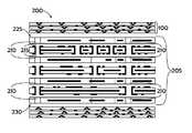
- FIG. 17shows a plurality of cores 200 attached according to one embodiment of the current invention wherein a metallurgical paste 210 creates an electrical connection between two vias with conductive surfaces 215 to create Z-axis interconnects 205 as known in the art and also the novel coreless buildup layer 100 are diffusion bonded to the upper surface 225 and lower surface 230 , respectively. Few or all of the metallurgical paste 210 can be replaced by conductive adhesive to create an electrical connection between two vias with conductive surfaces 215 to create Z-axis interconnects.
Landscapes
- Engineering & Computer Science (AREA)
- Manufacturing & Machinery (AREA)
- Microelectronics & Electronic Packaging (AREA)
- Production Of Multi-Layered Print Wiring Board (AREA)
Abstract
Description
- The present application is related to co-pending U.S. patent application Ser. No. ______ (EI-2-08-021-2) for CORELESS LAYER BUILDUP STRUCTURE WITH LGA and U.S. patent application Ser. No. ______ (EI-2-08-021-3) for CORELESS LAYER BUILDUP STRUCTURE WITH LGA AND JOINING LAYER, both incorporated by reference herein in their entirety.
- The present invention relates to circuit board manufacturing and preparation and, more specifically, to a structure wherein a core is built up utilizing at least partially to completely advanced thermoset resin or thermoplastics.
- A common procedure in circuit board processing involves laminating multiple cores together. However, generally, the cores are not electrically connected via to via during lamination. For example, one method involves first electrically connecting the cores using conductive pads. After lamination, a hole is drilled through the conductive pads and electroplated with copper to form the via.
- An alternative solution uses conductive adhesive to electrically attach vias during lamination. The conductive adhesive is placed onto a via and electrically connects the vias when the cores are laminated together. However, conductive adhesives contain plate-like structures greater than 0.5 mils in size. These plates tend to clog at the top of the holes. Therefore, the adhesives cannot be used effectively with thicker cores and smaller vias. Additionally, conductive adhesives require precious metal for good connections, making the products more expensive. Finally, a substantial number of manufacturing sites are not equipped to handle conductive adhesives. Consequently, significant costs may be required to modify current manufacturing sites to use conductive adhesives.
- As a result, there exists a need for a structure and method of attaching cores having vias with conductive surfaces without using a conductive material for the joining process such as that that is currently used.
- U.S. Pat. No. 6,465,084, by Curcio, et al granted Oct. 15, 2002, and U.S. Pat. No. 6,638,607, by Curcio, et al., granted Oct. 28, 2003 for METHOD AND STRUCTURE FOR PRODUCING Z-AXIS INTERCONNECTION ASSEMBLY OF PRINTED WIRING BOARD ELEMENTS disclose a method of forming a core for a composite wiring board. The core has an electrically conductive coating on at least one face of a dielectric substrate. At least one opening is formed through the substrate extending from one face to the other and through each conductive coating. An electrically conductive material is dispensed in each of the openings extending through the conducting coating. At least a portion of the surface of the conductive coating on one face is removed to allow a nub of the conductive material to extend above the substrate face and any remaining conductive material to thereby form a core that can be electrically joined face-to-face with a second core member or other circuitized structure.
- U.S. Pat. No. 6,969,436 by Curcio, et al., granted Nov. 29, 2005 for METHOD AND STRUCTURE FOR PRODUCING Z-AXIS INTERCONNECTION ASSEMBLY OF PRINTED WIRING BOARD ELEMENTS and U.S. Pat. No. 7,303,639, by Curcio, et al., granted Dec. 4, 2007 for METHOD FOR PRODUCING Z-AXIS INTERCONNECTION ASSEMBLY OF PRINTED WIRING BOARD ELEMENTS disclose a method of forming a member to form a composite wiring board. The member includes a dielectric substrate. Adhesive tape is applied to at least one face of said substrate. At least one opening is formed through the substrate extending from one face to the other and through each adhesive tape. An electrically conductive material is dispensed in each of the openings and partially cured. The adhesive tape is removed to allow a nub of the conductive material to extend above the substrate face to form a wiring structure with other elements.
- According to the present invention, there is provided a method and structure of attaching a plurality of cores. A substrate for use in a PC board has a coreless buildup layer and a metal layer disposed thereon. Optionally, a second metal layer can be provided with a dielectric layer between the two metal layers.
- A first aspect of the invention is directed to having coreless buildup layers consisting of thermoset resin. Each or alternate buildup layers are partially advanced to process circuitization and subsequently fully cured during final lamination process. Example of buildup layers: resin coated Cu based on filled epoxy or filled PPE, etc.
- A second aspect of the invention is directed to a method having coreless buildup layers consisting of thermoplastics. Each buildup layer is circuitized and subsequently laminated to get final structure. Example of buildup layers: Polyimide, liquid crystal polymer (LCP) or Teflon® based materials. Buildup layers an also be a mixture of thermoplastics such as LCP and polyimide. Here, LCP will melt and form bonding among the buildups. For LCP and Teflon mixtures, LCP will likewise melt and form bonding among the buildups.
- A third aspect of the invention is directed to a structure having coreless buildup layers consisting of thermoset and/or thermoplastic resin. Here the thermoset buildup layers are partially advanced to process circuitization and subsequently fully cured during a final lamination process.
- A fourth aspect of the invention is directed to a method having coreless buildup layers consist of thermoset and/or thermoplastic resin. Here thermoset buildup layers are fully cured and circuitized. Thermoplastic will melt and form bonding among the buildups.
- A fifth aspect of the invention is directed to a method having a metal surface: It can be metal or alloy or their mixture that will diffuse with each other during final bonding. All surfaces, some surfaces, or alternate surface can have low melting point metal or alloy surface finish where low melting melts during or after lamination and form metal-metal bonding.
- These and other features and advantages of this invention will be more readily understood from the following detailed description of the various aspects of the invention taken in conjunction with the accompanying drawings in which:
FIGS. 1-6 show a longitudinal, sectional view, somewhat diagrammatic, of the steps to form a core member according to one embodiment of the present invention;FIGS. 7 and 8 show the steps of laminating two core members together to form a printed wiring board according to one embodiment of the invention;FIGS. 9-13 show a longitudinal, sectional view, somewhat diagrammatic, of the steps to form a joining member according to another embodiment of the present invention;FIGS. 14 and 15 show the steps of laminating two core members together using a joining member formed according to this invention;FIG. 16 shows a section view of coreless buildup layer stack up; andFIG. 17 shows a plurality of cores attached according to one embodiment of the current invention wherein a metallurgical paste makes an electrical connection between two Z-interconnect vias with conductive surfaces and coreless buildup layers attached thereto.- It is noted that the drawings of the invention are not to scale. The drawings are merely schematic representations, not intended to portray specific parameters of the invention. The drawings are intended to depict only typical embodiments of the invention, and therefore should not be considered as limiting the scope of the invention. In the drawings, like numbering represents like elements between the drawings.
- For the sake of clarity and brevity, like elements and components of each embodiment will bear the same designations throughout the description.
- In the invention, a method and structure are provided for electrically joining a plurality of cores using thermoset resin and/or thermoplastic.
- Referring now to the drawings and, for the present, to
FIGS. 1-6 , the successive steps in forming acore member 10 for use in laminating to another core member to form a printed wiring board according to one embodiment of the invention are shown. As can be seen inFIG. 1 , thecore member 10 includes adielectric substrate 12 which has layers ofmetal coatings Dielectric substrate 12 can be any conventional dielectric, such as FR4 (a glass reinforced epoxy), polyimide, polytetrafluoroethylene or other suitable well known dielectric. In the embodiment shown inFIGS. 1-6 , themetal coatings - As shown in
FIG. 2 , preferably thecopper layer 14 is patterned to form circuit traces18 and thecopper layer 16 is patterned to form circuit traces20. Any conventional patterning process, such as by using a photoresist, exposing, developing and etching the exposed areas and then stripping the photoresist can be used. - As shown in
FIG. 3 , a film in the form ofadhesive tape 22 is applied over the circuit traces18 and the same type of film is applied over the circuit traces20. A particularly useful adhesive tape is a polyimide having a silicone adhesive. This is available from Dielectric Polymers, Inc. of Holyoke, Mass. This tape must be compatible with the conductive material and processes associated with the formatting of the core, which will be described presently. Other types of film material may be used, such as plating tapes NT-580, 582, 583, 590 and 590-2 manufactured by Dielectric Polymers, Inc. Thetape - Referring now to
FIG. 4 , a plurality of holes or openings, two of which are shown at26, are drilled through the entire composite, including theadhesive tape substrate 12. These holes oropenings 26 define the location of the conductive interconnect vias that will be formed. - Into the
openings 26 is deposited an electricallyconductive paste material 28, as shown inFIG. 5 . The filling of theseopenings 26 can be performed by screening, stenciling, flood coating, doctor blading, immersing or injecting. Various types of conductive material may be used. By the term “conductive paste” as used herein is meant an electrically conductive paste composition adapted for use in holes or openings of substrates as well as between conductors which form parts of conductive planes of such a substrate. Such a paste includes at least one organic binder component and, in one embodiment, at least one metallic component including a plurality of “microparticles.” In another embodiment, the paste includes such an organic binder in addition to the aforementioned microparticles. A preferred conductive polymer material is a conductive epoxy sold by National Starch and Chemical Company under the trademark “Ablebond 8175” (This was formerly sold by Ablestik Corporation) “Ablebond8175” is a silver filled thermosetting epoxy. Following the filling of theholes 26, as shown inFIG. 5 , the epoxy is B-staged which entails heating the material to a temperature of about 130° C. until the degree of cure is advanced from about 20% to about 80% complete cure. As will become apparent later, the film material should not be fully cured at this stage since it will be used to adhere to another conductive epoxy in another core element. Alternatively, a solder paste of tin lead, tin lead silver, tin silver copper, tin silver copper antimony or tin bismuth, which are commercially available, can be used and heated to reflow. - After the
conductive material 28 is partially cured, theadhesive tape FIG. 6 . As can be seen inFIG. 6 , the partially curedconductive material 28 extends above the circuit traces18 and20 a distance equal to the thickness of theadhesive tape - If the copper layers14 and16 have not been previously patterned, that can be done at this point. However, in general, it is preferred that the patterning to form the circuit traces18 and20 be done, as shown in
FIG. 2 , at that stage in the process so that theconductive material 28 is not subjected to the harsh chemical processes normally encountered in patterning material. - As can be seen in
FIG. 7 , twocore elements core elements FIGS. 7 and 8 , the letter suffixes a and b are used to denote similar structures in each core element.) As seen inFIG. 7 , a pre-drilledadhesive bonding film 30, such as the film sold under the trademark Pyralux LF by - Pyralux Corporation, is interposed between the two
cores film 30 has openings32 drilled therein which are positioned to align with the conductive fill material24a,24bin the twocore elements - Heat and pressure are applied to cause the two core members to bond together, with the Pyralux LF film acting as an adhesive bond material. Also, the
fill material core members FIG. 8 , to form a continuous Z-axis electrical connection between the circuit traces18a,18b,20aand20bon thecore element substrate 30 will fill around the circuit traces18band20a.The lamination process also advances the cure of theconductive fill material adhesive tape 22. An example of suitable dicing tape is Adwill D-series tape provided by Lintec Corporation. These tapes are comprised of a base material, such as PVC (poly vinyl chloride), or PET (polyethylene terephthalate), or PO (polyolefin) with an adhesive film that provides strong temporary adhesion. Alternatively, the adhesive could be provided on other base material, such as polyimide. - The adhesive layer provided on the base layer is formulated so that it provides strong initial adhesion but, upon exposure to UV (ultraviolet) radiation, its adhesion is diminished and it can be peeled and released without causing damage or leaving residue on the copper traces18 or the
dielectric layer 12. In such case, the backing must be transparent to UV radiation. Also, it is to be understood that thetape film material 30 could be a dry film epoxy adhesive which is B-staged, or thermoplastic LCP film or organic pre-preg typically comprising a layer of glass (typically fiberglass) cloth impregnated with a partially cured material, typically a B-stage epoxy resin or other film type adhesive dielectric layers and used to laminate thecore elements - Referring now to
FIGS. 9-13 , another embodiment of the present invention is shown which is useful in forming a joining member. Asubstrate 10 is provided which is preferably an adhesive dielectric material. For example, this could be an adhesive coated film (such as duPont Pyralux LF, which is a modified acrylic adhesive on a polyimide film) or a B-staged thermoset adhesive (such as IBM Dri-clad glass reinforced high glass transition dielectric material), or other film type adhesive dielectric layers, including materials such as Rogers 2800 Silica filled polytetrafluoroethylene. Thermoset resin coated Silica filled polytetrafluoroethylene or thermoset resin coated liquid crystal polymer (LCP) or LCP-Silica filled polytetrafluoroethylene-LCP or LCP-Polyimide-LCP type materials can also be used. In general, LCP bondply (available from Rogers) can be laminated with polyimide or Silica filled polytetrafluoroethylene to make LCP-Polyimide-LCP or LCP- Silica filled polytetrafluoroethylene-LCP mixed dielectric. - A plurality of holes, one of which is shown at26, is either mechanically or laser drilled through the
substrate 12 and through both of thetapes FIG. 11 . Aconductive material 28 of the same type as described with respect to FIGS. 1-6 is deposited in thehole 26 by the same techniques as previously described with respect toFIGS. 1-6 . After theconductive material 28 is remelted or cured, as previously described, theadhesive tapes FIG. 13 . Alternatively,tapes FIG. 13 ).- In
FIG. 11 a, theopening 26 is plated, preferably with copper, to form inner conductive layers. A preferred method of accomplishing this is to use a “flash” plating of electro-less copper. It is to be understood that forming plated layers35 is an optional step in forming a substrate as defined herein, but is preferred to further assure sound conductive paths in these portions of the structure. The next step, as also shown inFIG. 12 , involves the deposition ofconductive paste 28 within each of the platedopenings 26. Such deposition may be accomplished using conventional paste printing processes or dispensing through conventional needles. Significantly, the conductive paste as used in this embodiment includes a binder (preferably an organic binder) component and at least one metallic component. As defined herein, this metallic component is in the form of microparticles or nanoparticles or their mixtures, either as flakes or semi-colloidal powders. Metals may include copper, silver, gold, zinc, cadmium, palladium, iridium, ruthenium, osmium, rhodium, platinum, iron, cobalt, nickel, indium, tin, antimony, lead, bismuth and alloys thereof for the microparticles. - In one embodiment of the invention, a conductive paste having silver microparticles may be used, the paste including an anhydride epoxide as the organic binder. This paste preferably includes about 88% by weight of the silver microparticles and about 12% by weight of the anhydride epoxide. With the solder added to the microparticles as described below, the resulting paste has a decomposition temperature of approximately 340 degrees C., which, when considering the above high temperature dielectric material, is about ten degrees C. less than the 350 degrees C. temperature the dielectric can withstand during lamination. The average silver particles are each from about 0.01 microns to about 10 microns in diameter. In the case of both flat particles (flakes) and rod-like particles, thicknesses are each from about 0.01 micron to 10 micron.
- Although only one
opening 26 is depicted inFIG. 11 , this is meant to be representative only. In one example, a total of 2500 openings may be provided within a rectangular layer having dimensions of about 52.5 millimeters (mm) wide by about 52.5 mm long, and a thickness of about 0.175 mm. These 2500 paste filled nubs inFIG. 13 generate 3-D micro arrays. These kinds of conductive adhesive based 3-D micro array Z-interconnects are used to connect multiple electronic layers. FIGS. 6 and 13 show 3-D micro arrays for connecting several electronic layers starting from chip to board. Adhesives formulated using controlled-sized particles, ranging from nanometer scale to micrometer scale, were used to form micro arrays of contact pads having diameters ranging from 5 μm to 250 μm for internal and external interconnect applications. For example, micro arrays (not shown) with pads having 5-15 micron diameters are suitable for device level interconnects (chip to chip interconnects), whereas 50-75 μm and 250 μm diameters of the pads are suitable for chip carrier and board level interconnects, respectively.- As shown in
FIGS. 14 and 15 , a joining member formed according toFIGS. 9-13 is used to join two printedwiring boards 34. Thedielectric substrate 10 is adhesive or B-staged thermoset resin or thermoplastic polymer acting as a bonding member. Typically, the printed wiring boards will have adielectric substrate 36 with a plurality of internal conductive planes, one of which is shown at38, and plated throughholes 40. However, this is just illustrative as the joining member can be used to join many different types of printed wiring boards, the boards shown inFIGS. 14 and 15 being merely illustrative. - Alternatively, in
FIG. 14 , two printedwiring boards 34 can be flexible substrates and extended beyond the joininglayer 10. In that case,area 34 bonded withdielectric 10 is rigid and the rest of the area is free standing and flexible. In general, II-VI metal layers substrate made with flexible materials producesflexible substrate 34. One example of such material is sold under the product name “RO2800” dielectric material provided by Rogers Corporation, Rogers, Conn. - Again,
area 34 can be a substrate having embedded capacitors and resistors. Embedded capacitors can be a high dielectric constant ceramic filled dielectric (example barium titanate filled epoxy) layer. One example of such material are resin coated capacitive materials used as a buildup layers. The resistor can be a multilayer resistor foil laminated with the capacitor dielectric. For example, core can use 25 ohm per square material and 250 ohm per square inch material. This combination enables resistor ranges from 15 ohms through 30,000 ohms with efficient sizes for the embedded resistors. Here two printedwiring boards 34 having embedded capacitors and resistors are bonded with thedielectric substrate 10. Adhesive or B-staged thermoset resin or thermoplastic polymer acts as a bonding member. - Referring now to
FIG. 16 , acore 100 is shown having a plurality ofvias 130.Core 100 may comprise an epoxy core or any similar structure as commonly known in the art.Core 100 may include one or more planes120-122, which may include, for example, a power plane, signal plane, or a ground plane. Using via130 as an example, each via has aconductive surface 135 formed on a surface ofcore 100.Conductive surface 135 can comprise a thin layer of any solderable conductive material including, for example, a precious metal or copper. The joining concept forcore 100 is to use compression and heating to melt or diffuse the solder to create the laminate, thereby having metallic contacts between planes120-122 while not using a conductive paste. - Alternatively,
core 100 may include multiple planes and multiple dielectric layers. At least one or multiple dielectrics can be made with thermoplastic polymers. At least one of the thermoplastic layers may be larger than the joining layer and remain as an extended flexible layer. Flexible layer can be a capacitance layer or resistor foil laminated capacitance layer. One example of such flexible capacitance material is sold under the product name “RO2800” dielectric material by Rogers Corporation, Rogers, Conn. FIG. 17 shows a plurality ofcores 200 attached according to one embodiment of the current invention wherein ametallurgical paste 210 creates an electrical connection between two vias withconductive surfaces 215 to create Z-axis interconnects 205 as known in the art and also the novelcoreless buildup layer 100 are diffusion bonded to theupper surface 225 andlower surface 230, respectively. Few or all of themetallurgical paste 210 can be replaced by conductive adhesive to create an electrical connection between two vias withconductive surfaces 215 to create Z-axis interconnects.- Since other modifications and changes to the coreless layer buildup will be apparent to those skilled in the art, the invention is not considered limited to the description above for purposes of disclosure, and covers all changes and modifications which do not constitute departures from the true spirit and scope of this invention.
Claims (18)
Priority Applications (1)
| Application Number | Priority Date | Filing Date | Title |
|---|---|---|---|
| US12/764,993US8541687B2 (en) | 2010-04-22 | 2010-04-22 | Coreless layer buildup structure |
Applications Claiming Priority (1)
| Application Number | Priority Date | Filing Date | Title |
|---|---|---|---|
| US12/764,993US8541687B2 (en) | 2010-04-22 | 2010-04-22 | Coreless layer buildup structure |
Publications (2)
| Publication Number | Publication Date |
|---|---|
| US20120160547A1true US20120160547A1 (en) | 2012-06-28 |
| US8541687B2 US8541687B2 (en) | 2013-09-24 |
Family
ID=46315304
Family Applications (1)
| Application Number | Title | Priority Date | Filing Date |
|---|---|---|---|
| US12/764,993Expired - Fee RelatedUS8541687B2 (en) | 2010-04-22 | 2010-04-22 | Coreless layer buildup structure |
Country Status (1)
| Country | Link |
|---|---|
| US (1) | US8541687B2 (en) |
Cited By (7)
| Publication number | Priority date | Publication date | Assignee | Title |
|---|---|---|---|---|
| US20150195921A1 (en)* | 2012-09-20 | 2015-07-09 | Kuraray Co., Ltd. | Circuit board and method for manufacturing same |
| WO2016107061A1 (en)* | 2014-12-31 | 2016-07-07 | 广州兴森快捷电路科技有限公司 | Coreless board fabrication component and coreless board production method |
| WO2018069315A1 (en)* | 2016-10-11 | 2018-04-19 | Continental Automotive Gmbh | Method for producing a multi-layered printed circuit |
| WO2020128355A1 (en)* | 2018-12-21 | 2020-06-25 | Safran Electronics & Defense | Method for producing a backplane circuit board |
| JP2020528665A (en)* | 2017-06-28 | 2020-09-24 | カトラム・エルエルシー | Multilayer circuit board with intervening layers and conductive paste |
| US20220007499A1 (en)* | 2019-04-03 | 2022-01-06 | Murata Manufacturing Co., Ltd. | Module, terminal assembly, and method for producing module |
| US20220071014A1 (en)* | 2020-08-31 | 2022-03-03 | Liquid Wire Inc. | Flexible and stretchable structures |
Families Citing this family (2)
| Publication number | Priority date | Publication date | Assignee | Title |
|---|---|---|---|---|
| US9907190B1 (en)* | 2015-02-03 | 2018-02-27 | Amazon Technologies, Inc. | Composite structures and methods of making |
| US12108528B2 (en)* | 2019-03-26 | 2024-10-01 | Mitsubishi Materials Corporation | Insulating circuit board |
Citations (23)
| Publication number | Priority date | Publication date | Assignee | Title |
|---|---|---|---|---|
| US5542174A (en)* | 1994-09-15 | 1996-08-06 | Intel Corporation | Method and apparatus for forming solder balls and solder columns |
| US5869880A (en)* | 1995-12-29 | 1999-02-09 | International Business Machines Corporation | Structure and fabrication method for stackable, air-gap-containing low epsilon dielectric layers |
| US6274391B1 (en)* | 1992-10-26 | 2001-08-14 | Texas Instruments Incorporated | HDI land grid array packaged device having electrical and optical interconnects |
| US6284982B1 (en)* | 2000-08-18 | 2001-09-04 | Ga-Tek Inc. | Method and component for forming an embedded resistor in a multi-layer printed circuit |
| US20020189853A1 (en)* | 2001-06-15 | 2002-12-19 | Phoenix Precision Technology Corp. | BGA substrate with direct heat dissipating structure |
| US6562657B1 (en)* | 2000-08-22 | 2003-05-13 | Charles W. C. Lin | Semiconductor chip assembly with simultaneously electrolessly plated contact terminal and connection joint |
| JP2005064498A (en)* | 2003-08-13 | 2005-03-10 | Phoenix Precision Technology Corp | Semiconductor package board structure having metal protective layer for electrical connection pad, and manufacturing method for semiconductor packaging board structure |
| US6879492B2 (en)* | 2001-03-28 | 2005-04-12 | International Business Machines Corporation | Hyperbga buildup laminate |
| US20060043549A1 (en)* | 2004-09-01 | 2006-03-02 | Phoenix Precision Technology Corporation | Micro-electronic package structure and method for fabricating the same |
| US20060060557A1 (en)* | 2004-09-21 | 2006-03-23 | Sreenivasan Sidlgata V | Reverse tone patterning on surfaces having surface planarity perturbations |
| US7050304B2 (en)* | 2003-08-28 | 2006-05-23 | Phoenix Precision Technology Corporation | Heat sink structure with embedded electronic components for semiconductor package |
| US20070007033A1 (en)* | 2005-07-11 | 2007-01-11 | Endicott Interconnect Technologies, Inc. | Circuitized substrate with soler-coated microparticle paste connections, multilayered substrate assembly, electrical assembly and information handling system utilizing same and method of making said substrate |
| US20070045784A1 (en)* | 2005-08-25 | 2007-03-01 | Corisis David J | Lead frame-based semiconductor device packages incorporating at least one land grid array package and methods of fabrication |
| US7239525B2 (en)* | 2004-11-17 | 2007-07-03 | Phoenix Precision Technology Corporation | Circuit board structure with embedded selectable passive components and method for fabricating the same |
| US7242092B2 (en)* | 2005-02-02 | 2007-07-10 | Phoenix Precision Technology Corporation | Substrate assembly with direct electrical connection as a semiconductor package |
| JP2007214534A (en)* | 2006-02-09 | 2007-08-23 | Phoenix Precision Technology Corp | Manufacturing method of circuit board having conductive structure |
| US20070243387A1 (en)* | 2006-04-13 | 2007-10-18 | Lin Wendy W | Dual cure resin composite system and method of manufacturing the same |
| US20070246744A1 (en)* | 2006-04-19 | 2007-10-25 | Phoenix Precision Technology Corporation | Method of manufacturing a coreless package substrate and conductive structure of the substrate |
| US20080185704A1 (en)* | 2007-02-02 | 2008-08-07 | Phoenix Precision Technology Corporation | Carrier plate structure havign a chip embedded therein and the manufacturing method of the same |
| US7539022B2 (en)* | 2005-10-04 | 2009-05-26 | Phoenix Precision Technology Corporation | Chip embedded packaging structure |
| US7592706B2 (en)* | 2004-12-21 | 2009-09-22 | Phoenix Precision Technology Corporation | Multi-layer circuit board with fine pitches and fabricating method thereof |
| US7656040B2 (en)* | 2006-06-01 | 2010-02-02 | Phoenix Precision Technology Corporation | Stack structure of circuit board with semiconductor component embedded therein |
| US8017436B1 (en)* | 2007-12-10 | 2011-09-13 | Amkor Technology, Inc. | Thin substrate fabrication method and structure |
Family Cites Families (2)
| Publication number | Priority date | Publication date | Assignee | Title |
|---|---|---|---|---|
| US6465084B1 (en) | 2001-04-12 | 2002-10-15 | International Business Machines Corporation | Method and structure for producing Z-axis interconnection assembly of printed wiring board elements |
| US6638607B1 (en) | 2002-10-30 | 2003-10-28 | International Business Machines Corporation | Method and structure for producing Z-axis interconnection assembly of printed wiring board elements |
- 2010
- 2010-04-22USUS12/764,993patent/US8541687B2/ennot_activeExpired - Fee Related
Patent Citations (23)
| Publication number | Priority date | Publication date | Assignee | Title |
|---|---|---|---|---|
| US6274391B1 (en)* | 1992-10-26 | 2001-08-14 | Texas Instruments Incorporated | HDI land grid array packaged device having electrical and optical interconnects |
| US5542174A (en)* | 1994-09-15 | 1996-08-06 | Intel Corporation | Method and apparatus for forming solder balls and solder columns |
| US5869880A (en)* | 1995-12-29 | 1999-02-09 | International Business Machines Corporation | Structure and fabrication method for stackable, air-gap-containing low epsilon dielectric layers |
| US6284982B1 (en)* | 2000-08-18 | 2001-09-04 | Ga-Tek Inc. | Method and component for forming an embedded resistor in a multi-layer printed circuit |
| US6562657B1 (en)* | 2000-08-22 | 2003-05-13 | Charles W. C. Lin | Semiconductor chip assembly with simultaneously electrolessly plated contact terminal and connection joint |
| US6879492B2 (en)* | 2001-03-28 | 2005-04-12 | International Business Machines Corporation | Hyperbga buildup laminate |
| US20020189853A1 (en)* | 2001-06-15 | 2002-12-19 | Phoenix Precision Technology Corp. | BGA substrate with direct heat dissipating structure |
| JP2005064498A (en)* | 2003-08-13 | 2005-03-10 | Phoenix Precision Technology Corp | Semiconductor package board structure having metal protective layer for electrical connection pad, and manufacturing method for semiconductor packaging board structure |
| US7050304B2 (en)* | 2003-08-28 | 2006-05-23 | Phoenix Precision Technology Corporation | Heat sink structure with embedded electronic components for semiconductor package |
| US20060043549A1 (en)* | 2004-09-01 | 2006-03-02 | Phoenix Precision Technology Corporation | Micro-electronic package structure and method for fabricating the same |
| US20060060557A1 (en)* | 2004-09-21 | 2006-03-23 | Sreenivasan Sidlgata V | Reverse tone patterning on surfaces having surface planarity perturbations |
| US7239525B2 (en)* | 2004-11-17 | 2007-07-03 | Phoenix Precision Technology Corporation | Circuit board structure with embedded selectable passive components and method for fabricating the same |
| US7592706B2 (en)* | 2004-12-21 | 2009-09-22 | Phoenix Precision Technology Corporation | Multi-layer circuit board with fine pitches and fabricating method thereof |
| US7242092B2 (en)* | 2005-02-02 | 2007-07-10 | Phoenix Precision Technology Corporation | Substrate assembly with direct electrical connection as a semiconductor package |
| US20070007033A1 (en)* | 2005-07-11 | 2007-01-11 | Endicott Interconnect Technologies, Inc. | Circuitized substrate with soler-coated microparticle paste connections, multilayered substrate assembly, electrical assembly and information handling system utilizing same and method of making said substrate |
| US20070045784A1 (en)* | 2005-08-25 | 2007-03-01 | Corisis David J | Lead frame-based semiconductor device packages incorporating at least one land grid array package and methods of fabrication |
| US7539022B2 (en)* | 2005-10-04 | 2009-05-26 | Phoenix Precision Technology Corporation | Chip embedded packaging structure |
| JP2007214534A (en)* | 2006-02-09 | 2007-08-23 | Phoenix Precision Technology Corp | Manufacturing method of circuit board having conductive structure |
| US20070243387A1 (en)* | 2006-04-13 | 2007-10-18 | Lin Wendy W | Dual cure resin composite system and method of manufacturing the same |
| US20070246744A1 (en)* | 2006-04-19 | 2007-10-25 | Phoenix Precision Technology Corporation | Method of manufacturing a coreless package substrate and conductive structure of the substrate |
| US7656040B2 (en)* | 2006-06-01 | 2010-02-02 | Phoenix Precision Technology Corporation | Stack structure of circuit board with semiconductor component embedded therein |
| US20080185704A1 (en)* | 2007-02-02 | 2008-08-07 | Phoenix Precision Technology Corporation | Carrier plate structure havign a chip embedded therein and the manufacturing method of the same |
| US8017436B1 (en)* | 2007-12-10 | 2011-09-13 | Amkor Technology, Inc. | Thin substrate fabrication method and structure |
Cited By (13)
| Publication number | Priority date | Publication date | Assignee | Title |
|---|---|---|---|---|
| US20150195921A1 (en)* | 2012-09-20 | 2015-07-09 | Kuraray Co., Ltd. | Circuit board and method for manufacturing same |
| US9439303B2 (en)* | 2012-09-20 | 2016-09-06 | Kuraray Co., Ltd. | Circuit board and method for manufacturing same |
| WO2016107061A1 (en)* | 2014-12-31 | 2016-07-07 | 广州兴森快捷电路科技有限公司 | Coreless board fabrication component and coreless board production method |
| WO2018069315A1 (en)* | 2016-10-11 | 2018-04-19 | Continental Automotive Gmbh | Method for producing a multi-layered printed circuit |
| JP2020528665A (en)* | 2017-06-28 | 2020-09-24 | カトラム・エルエルシー | Multilayer circuit board with intervening layers and conductive paste |
| JP7209685B2 (en) | 2017-06-28 | 2023-01-20 | カトラム・エルエルシー | Multilayer circuit board with intervening layer and conductive paste |
| FR3091136A1 (en)* | 2018-12-21 | 2020-06-26 | Safran Electronics & Defense | method of manufacturing an electronic backplane card |
| WO2020128355A1 (en)* | 2018-12-21 | 2020-06-25 | Safran Electronics & Defense | Method for producing a backplane circuit board |
| US11350530B2 (en) | 2018-12-21 | 2022-05-31 | Safran Electronics & Defense | Method for producing a backplane circuit board |
| US20220007499A1 (en)* | 2019-04-03 | 2022-01-06 | Murata Manufacturing Co., Ltd. | Module, terminal assembly, and method for producing module |
| US11895769B2 (en)* | 2019-04-03 | 2024-02-06 | Murata Manufacturing Co., Ltd. | Module, terminal assembly, and method for producing module |
| US20220071014A1 (en)* | 2020-08-31 | 2022-03-03 | Liquid Wire Inc. | Flexible and stretchable structures |
| US12096563B2 (en)* | 2020-08-31 | 2024-09-17 | Liquid Wire Inc. | Flexible and stretchable structures |
Also Published As
| Publication number | Publication date |
|---|---|
| US8541687B2 (en) | 2013-09-24 |
Similar Documents
| Publication | Publication Date | Title |
|---|---|---|
| US8541687B2 (en) | Coreless layer buildup structure | |
| US20090241332A1 (en) | Circuitized substrate and method of making same | |
| KR940009175B1 (en) | Manufacturing method of multilayer printed board | |
| KR100534548B1 (en) | Enhancement of current-carrying capacity of a multilayer circuit board | |
| US6969436B2 (en) | Method and structure for producing Z-axis interconnection assembly of printed wiring board elements | |
| US9736948B2 (en) | Systems and methods of manufacturing printed circuit boards using blind and internal micro vias to couple subassemblies | |
| US7286367B2 (en) | Printed circuit board with a built-in passive device, manufacturing method of the printed circuit board, and elemental board for the printed circuit board | |
| JPH1145955A (en) | Element built-in multilayer wiring board and method of manufacturing the same | |
| US20120152605A1 (en) | Circuitized substrate with dielectric interposer assembly and method | |
| JPH11126978A (en) | Multilayer wiring board | |
| JPWO2004049772A1 (en) | Circuit board, multilayer wiring board, method for manufacturing circuit board, and method for manufacturing multilayer wiring board | |
| JP2008124459A (en) | Manufacturing method of circuit board which has solder paste connection part | |
| US9351408B2 (en) | Coreless layer buildup structure with LGA and joining layer | |
| JP2008103640A (en) | Multilayer wiring board | |
| JP2010232249A (en) | Multilayer printed wiring board and manufacturing method of the same | |
| US6851599B2 (en) | Method for producing multilayer wiring circuit board | |
| JPH07263828A (en) | Printed wiring board and manufacturing method thereof | |
| US8536459B2 (en) | Coreless layer buildup structure with LGA | |
| JPH08330736A (en) | Multilayer board and manufacture thereof | |
| JPH08316598A (en) | Printed wiring board and manufacturing method thereof | |
| JP3440174B2 (en) | Multilayer printed wiring board and method of manufacturing the same | |
| WO1995013901A1 (en) | Metallurgically bonded polymer vias | |
| JP2003023256A (en) | Printed wiring board and method of manufacturing the same | |
| JP2005109188A (en) | Circuit board and multilayer board, and method for manufacturing circuit board and multilayer board | |
| JP2004103716A (en) | Multilayer wiring board, base material for multilayer wiring board, and method of manufacturing the same |
Legal Events
| Date | Code | Title | Description |
|---|---|---|---|
| AS | Assignment | Owner name:PNC BANK, NATIONAL ASSOCIATION, PENNSYLVANIA Free format text:SECURITY AGREEMENT;ASSIGNORS:ENDICOTT INTERCONNECT TECHNOLOGIES, INC.;EI TRANSPORTATION COMPANY LLC;ENDICOTT MEDTECH, INC.;REEL/FRAME:028230/0798 Effective date:20120210 | |
| AS | Assignment | Owner name:INTEGRIAN HOLDINGS, LLC, NEW YORK Free format text:ASSIGNMENT OF SECURITY AGREEMENT;ASSIGNOR:PNC BANK, NATIONAL ASSOCIATION;REEL/FRAME:029938/0823 Effective date:20130306 | |
| AS | Assignment | Owner name:M&T BANK, NEW YORK Free format text:SECURITY AGREEMENT;ASSIGNORS:ENDICOTT INTERCONNECT TECHNOLOGIES, INC.;EI TRANSPORTATION COMPANY LLC;ENDICOTT MEDTECH, INC.;AND OTHERS;REEL/FRAME:030359/0057 Effective date:20130313 | |
| AS | Assignment | Owner name:MAINES, WILLIAM, NEW YORK Free format text:SECURITY AGREEMENT;ASSIGNOR:ENDICOTT INTERCONNECT TECHNOLOGIES, INC.;REEL/FRAME:030599/0918 Effective date:20130612 Owner name:MAINES, DAVID, NEW YORK Free format text:SECURITY AGREEMENT;ASSIGNOR:ENDICOTT INTERCONNECT TECHNOLOGIES, INC.;REEL/FRAME:030599/0918 Effective date:20130612 | |
| STCF | Information on status: patent grant | Free format text:PATENTED CASE | |
| FEPP | Fee payment procedure | Free format text:PAYOR NUMBER ASSIGNED (ORIGINAL EVENT CODE: ASPN); ENTITY STATUS OF PATENT OWNER: LARGE ENTITY Free format text:PAT HOLDER CLAIMS SMALL ENTITY STATUS, ENTITY STATUS SET TO SMALL (ORIGINAL EVENT CODE: LTOS); ENTITY STATUS OF PATENT OWNER: LARGE ENTITY | |
| AS | Assignment | Owner name:ENDICOTT INTERCONNECT TECHNOLOGIES, INC., NEW YORK Free format text:RELEASE BY SECURED PARTY;ASSIGNORS:MAINES, WILLIAM;MAINES, DAVID;REEL/FRAME:035098/0968 Effective date:20150130 | |
| AS | Assignment | Owner name:I3 ELECTRONICS, INC., NEW YORK Free format text:ASSIGNMENT OF ASSIGNORS INTEREST;ASSIGNOR:ENDICOTT INTERCONNECT TECHNOLOGIES, INC.;REEL/FRAME:035442/0569 Effective date:20150415 | |
| AS | Assignment | Owner name:M&T BANK, NEW YORK Free format text:SECURITY INTEREST;ASSIGNOR:I3 ELECTRONICS, INC.;REEL/FRAME:040608/0626 Effective date:20161103 | |
| FPAY | Fee payment | Year of fee payment:4 | |
| AS | Assignment | Owner name:TTM TECHNOLOGIES NORTH AMERICA, LLC, MISSOURI Free format text:ASSIGNMENT OF ASSIGNORS INTEREST;ASSIGNOR:I3 ELECTRONICS, INC.;REEL/FRAME:049758/0265 Effective date:20190612 | |
| FEPP | Fee payment procedure | Free format text:ENTITY STATUS SET TO UNDISCOUNTED (ORIGINAL EVENT CODE: BIG.); ENTITY STATUS OF PATENT OWNER: LARGE ENTITY | |
| FEPP | Fee payment procedure | Free format text:MAINTENANCE FEE REMINDER MAILED (ORIGINAL EVENT CODE: REM.); ENTITY STATUS OF PATENT OWNER: LARGE ENTITY | |
| LAPS | Lapse for failure to pay maintenance fees | Free format text:PATENT EXPIRED FOR FAILURE TO PAY MAINTENANCE FEES (ORIGINAL EVENT CODE: EXP.); ENTITY STATUS OF PATENT OWNER: LARGE ENTITY | |
| STCH | Information on status: patent discontinuation | Free format text:PATENT EXPIRED DUE TO NONPAYMENT OF MAINTENANCE FEES UNDER 37 CFR 1.362 | |
| FP | Lapsed due to failure to pay maintenance fee | Effective date:20210924 |