US20120155055A1 - Semiconductor chip assembly and method for making same - Google Patents
Semiconductor chip assembly and method for making sameDownload PDFInfo
- Publication number
- US20120155055A1 US20120155055A1US13/157,722US201113157722AUS2012155055A1US 20120155055 A1US20120155055 A1US 20120155055A1US 201113157722 AUS201113157722 AUS 201113157722AUS 2012155055 A1US2012155055 A1US 2012155055A1
- Authority
- US
- United States
- Prior art keywords
- dielectric layer
- conductive
- microelectronic
- microelectronic assembly
- contacts
- Prior art date
- Legal status (The legal status is an assumption and is not a legal conclusion. Google has not performed a legal analysis and makes no representation as to the accuracy of the status listed.)
- Granted
Links
Images


Classifications
- H—ELECTRICITY
- H01—ELECTRIC ELEMENTS
- H01L—SEMICONDUCTOR DEVICES NOT COVERED BY CLASS H10
- H01L24/00—Arrangements for connecting or disconnecting semiconductor or solid-state bodies; Methods or apparatus related thereto
- H01L24/80—Methods for connecting semiconductor or other solid state bodies using means for bonding being attached to, or being formed on, the surface to be connected
- H01L24/81—Methods for connecting semiconductor or other solid state bodies using means for bonding being attached to, or being formed on, the surface to be connected using a bump connector
- B—PERFORMING OPERATIONS; TRANSPORTING
- B23—MACHINE TOOLS; METAL-WORKING NOT OTHERWISE PROVIDED FOR
- B23K—SOLDERING OR UNSOLDERING; WELDING; CLADDING OR PLATING BY SOLDERING OR WELDING; CUTTING BY APPLYING HEAT LOCALLY, e.g. FLAME CUTTING; WORKING BY LASER BEAM
- B23K1/00—Soldering, e.g. brazing, or unsoldering
- B23K1/0008—Soldering, e.g. brazing, or unsoldering specially adapted for particular articles or work
- B23K1/0016—Brazing of electronic components
- H—ELECTRICITY
- H01—ELECTRIC ELEMENTS
- H01L—SEMICONDUCTOR DEVICES NOT COVERED BY CLASS H10
- H01L21/00—Processes or apparatus adapted for the manufacture or treatment of semiconductor or solid state devices or of parts thereof
- H01L21/02—Manufacture or treatment of semiconductor devices or of parts thereof
- H01L21/04—Manufacture or treatment of semiconductor devices or of parts thereof the devices having potential barriers, e.g. a PN junction, depletion layer or carrier concentration layer
- H01L21/48—Manufacture or treatment of parts, e.g. containers, prior to assembly of the devices, using processes not provided for in a single one of the groups H01L21/18 - H01L21/326 or H10D48/04 - H10D48/07
- H01L21/4814—Conductive parts
- H01L21/4846—Leads on or in insulating or insulated substrates, e.g. metallisation
- H01L21/4857—Multilayer substrates
- H—ELECTRICITY
- H01—ELECTRIC ELEMENTS
- H01L—SEMICONDUCTOR DEVICES NOT COVERED BY CLASS H10
- H01L21/00—Processes or apparatus adapted for the manufacture or treatment of semiconductor or solid state devices or of parts thereof
- H01L21/02—Manufacture or treatment of semiconductor devices or of parts thereof
- H01L21/04—Manufacture or treatment of semiconductor devices or of parts thereof the devices having potential barriers, e.g. a PN junction, depletion layer or carrier concentration layer
- H01L21/48—Manufacture or treatment of parts, e.g. containers, prior to assembly of the devices, using processes not provided for in a single one of the groups H01L21/18 - H01L21/326 or H10D48/04 - H10D48/07
- H01L21/4814—Conductive parts
- H01L21/4846—Leads on or in insulating or insulated substrates, e.g. metallisation
- H01L21/486—Via connections through the substrate with or without pins
- H—ELECTRICITY
- H01—ELECTRIC ELEMENTS
- H01L—SEMICONDUCTOR DEVICES NOT COVERED BY CLASS H10
- H01L21/00—Processes or apparatus adapted for the manufacture or treatment of semiconductor or solid state devices or of parts thereof
- H01L21/02—Manufacture or treatment of semiconductor devices or of parts thereof
- H01L21/04—Manufacture or treatment of semiconductor devices or of parts thereof the devices having potential barriers, e.g. a PN junction, depletion layer or carrier concentration layer
- H01L21/50—Assembly of semiconductor devices using processes or apparatus not provided for in a single one of the groups H01L21/18 - H01L21/326 or H10D48/04 - H10D48/07 e.g. sealing of a cap to a base of a container
- H01L21/56—Encapsulations, e.g. encapsulation layers, coatings
- H01L21/563—Encapsulation of active face of flip-chip device, e.g. underfilling or underencapsulation of flip-chip, encapsulation preform on chip or mounting substrate
- H—ELECTRICITY
- H01—ELECTRIC ELEMENTS
- H01L—SEMICONDUCTOR DEVICES NOT COVERED BY CLASS H10
- H01L23/00—Details of semiconductor or other solid state devices
- H01L23/48—Arrangements for conducting electric current to or from the solid state body in operation, e.g. leads, terminal arrangements ; Selection of materials therefor
- H01L23/488—Arrangements for conducting electric current to or from the solid state body in operation, e.g. leads, terminal arrangements ; Selection of materials therefor consisting of soldered or bonded constructions
- H01L23/498—Leads, i.e. metallisations or lead-frames on insulating substrates, e.g. chip carriers
- H01L23/49811—Additional leads joined to the metallisation on the insulating substrate, e.g. pins, bumps, wires, flat leads
- H—ELECTRICITY
- H01—ELECTRIC ELEMENTS
- H01L—SEMICONDUCTOR DEVICES NOT COVERED BY CLASS H10
- H01L23/00—Details of semiconductor or other solid state devices
- H01L23/562—Protection against mechanical damage
- H—ELECTRICITY
- H05—ELECTRIC TECHNIQUES NOT OTHERWISE PROVIDED FOR
- H05K—PRINTED CIRCUITS; CASINGS OR CONSTRUCTIONAL DETAILS OF ELECTRIC APPARATUS; MANUFACTURE OF ASSEMBLAGES OF ELECTRICAL COMPONENTS
- H05K1/00—Printed circuits
- H05K1/02—Details
- H05K1/11—Printed elements for providing electric connections to or between printed circuits
- H05K1/111—Pads for surface mounting, e.g. lay-out
- H05K1/112—Pads for surface mounting, e.g. lay-out directly combined with via connections
- H05K1/113—Via provided in pad; Pad over filled via
- H—ELECTRICITY
- H05—ELECTRIC TECHNIQUES NOT OTHERWISE PROVIDED FOR
- H05K—PRINTED CIRCUITS; CASINGS OR CONSTRUCTIONAL DETAILS OF ELECTRIC APPARATUS; MANUFACTURE OF ASSEMBLAGES OF ELECTRICAL COMPONENTS
- H05K3/00—Apparatus or processes for manufacturing printed circuits
- H05K3/30—Assembling printed circuits with electric components, e.g. with resistor
- H05K3/32—Assembling printed circuits with electric components, e.g. with resistor electrically connecting electric components or wires to printed circuits
- H05K3/34—Assembling printed circuits with electric components, e.g. with resistor electrically connecting electric components or wires to printed circuits by soldering
- H05K3/341—Surface mounted components
- H—ELECTRICITY
- H05—ELECTRIC TECHNIQUES NOT OTHERWISE PROVIDED FOR
- H05K—PRINTED CIRCUITS; CASINGS OR CONSTRUCTIONAL DETAILS OF ELECTRIC APPARATUS; MANUFACTURE OF ASSEMBLAGES OF ELECTRICAL COMPONENTS
- H05K3/00—Apparatus or processes for manufacturing printed circuits
- H05K3/40—Forming printed elements for providing electric connections to or between printed circuits
- H05K3/4007—Surface contacts, e.g. bumps
- H—ELECTRICITY
- H01—ELECTRIC ELEMENTS
- H01L—SEMICONDUCTOR DEVICES NOT COVERED BY CLASS H10
- H01L2224/00—Indexing scheme for arrangements for connecting or disconnecting semiconductor or solid-state bodies and methods related thereto as covered by H01L24/00
- H01L2224/01—Means for bonding being attached to, or being formed on, the surface to be connected, e.g. chip-to-package, die-attach, "first-level" interconnects; Manufacturing methods related thereto
- H01L2224/10—Bump connectors; Manufacturing methods related thereto
- H01L2224/12—Structure, shape, material or disposition of the bump connectors prior to the connecting process
- H01L2224/13—Structure, shape, material or disposition of the bump connectors prior to the connecting process of an individual bump connector
- H01L2224/13001—Core members of the bump connector
- H01L2224/1301—Shape
- H01L2224/13016—Shape in side view
- H01L2224/13017—Shape in side view being non uniform along the bump connector
- H—ELECTRICITY
- H01—ELECTRIC ELEMENTS
- H01L—SEMICONDUCTOR DEVICES NOT COVERED BY CLASS H10
- H01L2224/00—Indexing scheme for arrangements for connecting or disconnecting semiconductor or solid-state bodies and methods related thereto as covered by H01L24/00
- H01L2224/01—Means for bonding being attached to, or being formed on, the surface to be connected, e.g. chip-to-package, die-attach, "first-level" interconnects; Manufacturing methods related thereto
- H01L2224/10—Bump connectors; Manufacturing methods related thereto
- H01L2224/12—Structure, shape, material or disposition of the bump connectors prior to the connecting process
- H01L2224/13—Structure, shape, material or disposition of the bump connectors prior to the connecting process of an individual bump connector
- H01L2224/13001—Core members of the bump connector
- H01L2224/1302—Disposition
- H01L2224/13023—Disposition the whole bump connector protruding from the surface
- H—ELECTRICITY
- H01—ELECTRIC ELEMENTS
- H01L—SEMICONDUCTOR DEVICES NOT COVERED BY CLASS H10
- H01L2224/00—Indexing scheme for arrangements for connecting or disconnecting semiconductor or solid-state bodies and methods related thereto as covered by H01L24/00
- H01L2224/01—Means for bonding being attached to, or being formed on, the surface to be connected, e.g. chip-to-package, die-attach, "first-level" interconnects; Manufacturing methods related thereto
- H01L2224/10—Bump connectors; Manufacturing methods related thereto
- H01L2224/12—Structure, shape, material or disposition of the bump connectors prior to the connecting process
- H01L2224/13—Structure, shape, material or disposition of the bump connectors prior to the connecting process of an individual bump connector
- H01L2224/13001—Core members of the bump connector
- H01L2224/13099—Material
- H01L2224/131—Material with a principal constituent of the material being a metal or a metalloid, e.g. boron [B], silicon [Si], germanium [Ge], arsenic [As], antimony [Sb], tellurium [Te] and polonium [Po], and alloys thereof
- H01L2224/13101—Material with a principal constituent of the material being a metal or a metalloid, e.g. boron [B], silicon [Si], germanium [Ge], arsenic [As], antimony [Sb], tellurium [Te] and polonium [Po], and alloys thereof the principal constituent melting at a temperature of less than 400°C
- H01L2224/13109—Indium [In] as principal constituent
- H—ELECTRICITY
- H01—ELECTRIC ELEMENTS
- H01L—SEMICONDUCTOR DEVICES NOT COVERED BY CLASS H10
- H01L2224/00—Indexing scheme for arrangements for connecting or disconnecting semiconductor or solid-state bodies and methods related thereto as covered by H01L24/00
- H01L2224/01—Means for bonding being attached to, or being formed on, the surface to be connected, e.g. chip-to-package, die-attach, "first-level" interconnects; Manufacturing methods related thereto
- H01L2224/10—Bump connectors; Manufacturing methods related thereto
- H01L2224/12—Structure, shape, material or disposition of the bump connectors prior to the connecting process
- H01L2224/13—Structure, shape, material or disposition of the bump connectors prior to the connecting process of an individual bump connector
- H01L2224/13001—Core members of the bump connector
- H01L2224/13099—Material
- H01L2224/131—Material with a principal constituent of the material being a metal or a metalloid, e.g. boron [B], silicon [Si], germanium [Ge], arsenic [As], antimony [Sb], tellurium [Te] and polonium [Po], and alloys thereof
- H01L2224/13101—Material with a principal constituent of the material being a metal or a metalloid, e.g. boron [B], silicon [Si], germanium [Ge], arsenic [As], antimony [Sb], tellurium [Te] and polonium [Po], and alloys thereof the principal constituent melting at a temperature of less than 400°C
- H01L2224/13111—Tin [Sn] as principal constituent
- H—ELECTRICITY
- H01—ELECTRIC ELEMENTS
- H01L—SEMICONDUCTOR DEVICES NOT COVERED BY CLASS H10
- H01L2224/00—Indexing scheme for arrangements for connecting or disconnecting semiconductor or solid-state bodies and methods related thereto as covered by H01L24/00
- H01L2224/01—Means for bonding being attached to, or being formed on, the surface to be connected, e.g. chip-to-package, die-attach, "first-level" interconnects; Manufacturing methods related thereto
- H01L2224/10—Bump connectors; Manufacturing methods related thereto
- H01L2224/12—Structure, shape, material or disposition of the bump connectors prior to the connecting process
- H01L2224/13—Structure, shape, material or disposition of the bump connectors prior to the connecting process of an individual bump connector
- H01L2224/13001—Core members of the bump connector
- H01L2224/13099—Material
- H01L2224/131—Material with a principal constituent of the material being a metal or a metalloid, e.g. boron [B], silicon [Si], germanium [Ge], arsenic [As], antimony [Sb], tellurium [Te] and polonium [Po], and alloys thereof
- H01L2224/13138—Material with a principal constituent of the material being a metal or a metalloid, e.g. boron [B], silicon [Si], germanium [Ge], arsenic [As], antimony [Sb], tellurium [Te] and polonium [Po], and alloys thereof the principal constituent melting at a temperature of greater than or equal to 950°C and less than 1550°C
- H01L2224/13147—Copper [Cu] as principal constituent
- H—ELECTRICITY
- H01—ELECTRIC ELEMENTS
- H01L—SEMICONDUCTOR DEVICES NOT COVERED BY CLASS H10
- H01L2224/00—Indexing scheme for arrangements for connecting or disconnecting semiconductor or solid-state bodies and methods related thereto as covered by H01L24/00
- H01L2224/01—Means for bonding being attached to, or being formed on, the surface to be connected, e.g. chip-to-package, die-attach, "first-level" interconnects; Manufacturing methods related thereto
- H01L2224/10—Bump connectors; Manufacturing methods related thereto
- H01L2224/12—Structure, shape, material or disposition of the bump connectors prior to the connecting process
- H01L2224/13—Structure, shape, material or disposition of the bump connectors prior to the connecting process of an individual bump connector
- H01L2224/13001—Core members of the bump connector
- H01L2224/13099—Material
- H01L2224/13198—Material with a principal constituent of the material being a combination of two or more materials in the form of a matrix with a filler, i.e. being a hybrid material, e.g. segmented structures, foams
- H01L2224/13298—Fillers
- H01L2224/13299—Base material
- H01L2224/133—Base material with a principal constituent of the material being a metal or a metalloid, e.g. boron [B], silicon [Si], germanium [Ge], arsenic [As], antimony [Sb], tellurium [Te] and polonium [Po], and alloys thereof
- H—ELECTRICITY
- H01—ELECTRIC ELEMENTS
- H01L—SEMICONDUCTOR DEVICES NOT COVERED BY CLASS H10
- H01L2224/00—Indexing scheme for arrangements for connecting or disconnecting semiconductor or solid-state bodies and methods related thereto as covered by H01L24/00
- H01L2224/01—Means for bonding being attached to, or being formed on, the surface to be connected, e.g. chip-to-package, die-attach, "first-level" interconnects; Manufacturing methods related thereto
- H01L2224/10—Bump connectors; Manufacturing methods related thereto
- H01L2224/15—Structure, shape, material or disposition of the bump connectors after the connecting process
- H01L2224/16—Structure, shape, material or disposition of the bump connectors after the connecting process of an individual bump connector
- H01L2224/161—Disposition
- H01L2224/16151—Disposition the bump connector connecting between a semiconductor or solid-state body and an item not being a semiconductor or solid-state body, e.g. chip-to-substrate, chip-to-passive
- H01L2224/16221—Disposition the bump connector connecting between a semiconductor or solid-state body and an item not being a semiconductor or solid-state body, e.g. chip-to-substrate, chip-to-passive the body and the item being stacked
- H01L2224/16225—Disposition the bump connector connecting between a semiconductor or solid-state body and an item not being a semiconductor or solid-state body, e.g. chip-to-substrate, chip-to-passive the body and the item being stacked the item being non-metallic, e.g. insulating substrate with or without metallisation
- H01L2224/16227—Disposition the bump connector connecting between a semiconductor or solid-state body and an item not being a semiconductor or solid-state body, e.g. chip-to-substrate, chip-to-passive the body and the item being stacked the item being non-metallic, e.g. insulating substrate with or without metallisation the bump connector connecting to a bond pad of the item
- H—ELECTRICITY
- H01—ELECTRIC ELEMENTS
- H01L—SEMICONDUCTOR DEVICES NOT COVERED BY CLASS H10
- H01L2224/00—Indexing scheme for arrangements for connecting or disconnecting semiconductor or solid-state bodies and methods related thereto as covered by H01L24/00
- H01L2224/01—Means for bonding being attached to, or being formed on, the surface to be connected, e.g. chip-to-package, die-attach, "first-level" interconnects; Manufacturing methods related thereto
- H01L2224/10—Bump connectors; Manufacturing methods related thereto
- H01L2224/15—Structure, shape, material or disposition of the bump connectors after the connecting process
- H01L2224/16—Structure, shape, material or disposition of the bump connectors after the connecting process of an individual bump connector
- H01L2224/161—Disposition
- H01L2224/16151—Disposition the bump connector connecting between a semiconductor or solid-state body and an item not being a semiconductor or solid-state body, e.g. chip-to-substrate, chip-to-passive
- H01L2224/16221—Disposition the bump connector connecting between a semiconductor or solid-state body and an item not being a semiconductor or solid-state body, e.g. chip-to-substrate, chip-to-passive the body and the item being stacked
- H01L2224/16225—Disposition the bump connector connecting between a semiconductor or solid-state body and an item not being a semiconductor or solid-state body, e.g. chip-to-substrate, chip-to-passive the body and the item being stacked the item being non-metallic, e.g. insulating substrate with or without metallisation
- H01L2224/16238—Disposition the bump connector connecting between a semiconductor or solid-state body and an item not being a semiconductor or solid-state body, e.g. chip-to-substrate, chip-to-passive the body and the item being stacked the item being non-metallic, e.g. insulating substrate with or without metallisation the bump connector connecting to a bonding area protruding from the surface of the item
- H—ELECTRICITY
- H01—ELECTRIC ELEMENTS
- H01L—SEMICONDUCTOR DEVICES NOT COVERED BY CLASS H10
- H01L2224/00—Indexing scheme for arrangements for connecting or disconnecting semiconductor or solid-state bodies and methods related thereto as covered by H01L24/00
- H01L2224/01—Means for bonding being attached to, or being formed on, the surface to be connected, e.g. chip-to-package, die-attach, "first-level" interconnects; Manufacturing methods related thereto
- H01L2224/26—Layer connectors, e.g. plate connectors, solder or adhesive layers; Manufacturing methods related thereto
- H01L2224/31—Structure, shape, material or disposition of the layer connectors after the connecting process
- H01L2224/32—Structure, shape, material or disposition of the layer connectors after the connecting process of an individual layer connector
- H01L2224/321—Disposition
- H01L2224/32151—Disposition the layer connector connecting between a semiconductor or solid-state body and an item not being a semiconductor or solid-state body, e.g. chip-to-substrate, chip-to-passive
- H01L2224/32221—Disposition the layer connector connecting between a semiconductor or solid-state body and an item not being a semiconductor or solid-state body, e.g. chip-to-substrate, chip-to-passive the body and the item being stacked
- H01L2224/32225—Disposition the layer connector connecting between a semiconductor or solid-state body and an item not being a semiconductor or solid-state body, e.g. chip-to-substrate, chip-to-passive the body and the item being stacked the item being non-metallic, e.g. insulating substrate with or without metallisation
- H—ELECTRICITY
- H01—ELECTRIC ELEMENTS
- H01L—SEMICONDUCTOR DEVICES NOT COVERED BY CLASS H10
- H01L2224/00—Indexing scheme for arrangements for connecting or disconnecting semiconductor or solid-state bodies and methods related thereto as covered by H01L24/00
- H01L2224/73—Means for bonding being of different types provided for in two or more of groups H01L2224/10, H01L2224/18, H01L2224/26, H01L2224/34, H01L2224/42, H01L2224/50, H01L2224/63, H01L2224/71
- H01L2224/732—Location after the connecting process
- H01L2224/73201—Location after the connecting process on the same surface
- H01L2224/73203—Bump and layer connectors
- H01L2224/73204—Bump and layer connectors the bump connector being embedded into the layer connector
- H—ELECTRICITY
- H01—ELECTRIC ELEMENTS
- H01L—SEMICONDUCTOR DEVICES NOT COVERED BY CLASS H10
- H01L2224/00—Indexing scheme for arrangements for connecting or disconnecting semiconductor or solid-state bodies and methods related thereto as covered by H01L24/00
- H01L2224/80—Methods for connecting semiconductor or other solid state bodies using means for bonding being attached to, or being formed on, the surface to be connected
- H01L2224/81—Methods for connecting semiconductor or other solid state bodies using means for bonding being attached to, or being formed on, the surface to be connected using a bump connector
- H01L2224/8119—Arrangement of the bump connectors prior to mounting
- H01L2224/81192—Arrangement of the bump connectors prior to mounting wherein the bump connectors are disposed only on another item or body to be connected to the semiconductor or solid-state body
- H—ELECTRICITY
- H01—ELECTRIC ELEMENTS
- H01L—SEMICONDUCTOR DEVICES NOT COVERED BY CLASS H10
- H01L2224/00—Indexing scheme for arrangements for connecting or disconnecting semiconductor or solid-state bodies and methods related thereto as covered by H01L24/00
- H01L2224/80—Methods for connecting semiconductor or other solid state bodies using means for bonding being attached to, or being formed on, the surface to be connected
- H01L2224/81—Methods for connecting semiconductor or other solid state bodies using means for bonding being attached to, or being formed on, the surface to be connected using a bump connector
- H01L2224/8119—Arrangement of the bump connectors prior to mounting
- H01L2224/81193—Arrangement of the bump connectors prior to mounting wherein the bump connectors are disposed on both the semiconductor or solid-state body and another item or body to be connected to the semiconductor or solid-state body
- H—ELECTRICITY
- H01—ELECTRIC ELEMENTS
- H01L—SEMICONDUCTOR DEVICES NOT COVERED BY CLASS H10
- H01L2224/00—Indexing scheme for arrangements for connecting or disconnecting semiconductor or solid-state bodies and methods related thereto as covered by H01L24/00
- H01L2224/80—Methods for connecting semiconductor or other solid state bodies using means for bonding being attached to, or being formed on, the surface to be connected
- H01L2224/81—Methods for connecting semiconductor or other solid state bodies using means for bonding being attached to, or being formed on, the surface to be connected using a bump connector
- H01L2224/8138—Bonding interfaces outside the semiconductor or solid-state body
- H—ELECTRICITY
- H01—ELECTRIC ELEMENTS
- H01L—SEMICONDUCTOR DEVICES NOT COVERED BY CLASS H10
- H01L2224/00—Indexing scheme for arrangements for connecting or disconnecting semiconductor or solid-state bodies and methods related thereto as covered by H01L24/00
- H01L2224/80—Methods for connecting semiconductor or other solid state bodies using means for bonding being attached to, or being formed on, the surface to be connected
- H01L2224/81—Methods for connecting semiconductor or other solid state bodies using means for bonding being attached to, or being formed on, the surface to be connected using a bump connector
- H01L2224/818—Bonding techniques
- H01L2224/81801—Soldering or alloying
- H—ELECTRICITY
- H01—ELECTRIC ELEMENTS
- H01L—SEMICONDUCTOR DEVICES NOT COVERED BY CLASS H10
- H01L2224/00—Indexing scheme for arrangements for connecting or disconnecting semiconductor or solid-state bodies and methods related thereto as covered by H01L24/00
- H01L2224/80—Methods for connecting semiconductor or other solid state bodies using means for bonding being attached to, or being formed on, the surface to be connected
- H01L2224/81—Methods for connecting semiconductor or other solid state bodies using means for bonding being attached to, or being formed on, the surface to be connected using a bump connector
- H01L2224/818—Bonding techniques
- H01L2224/8185—Bonding techniques using a polymer adhesive, e.g. an adhesive based on silicone, epoxy, polyimide, polyester
- H—ELECTRICITY
- H01—ELECTRIC ELEMENTS
- H01L—SEMICONDUCTOR DEVICES NOT COVERED BY CLASS H10
- H01L2224/00—Indexing scheme for arrangements for connecting or disconnecting semiconductor or solid-state bodies and methods related thereto as covered by H01L24/00
- H01L2224/80—Methods for connecting semiconductor or other solid state bodies using means for bonding being attached to, or being formed on, the surface to be connected
- H01L2224/83—Methods for connecting semiconductor or other solid state bodies using means for bonding being attached to, or being formed on, the surface to be connected using a layer connector
- H01L2224/831—Methods for connecting semiconductor or other solid state bodies using means for bonding being attached to, or being formed on, the surface to be connected using a layer connector the layer connector being supplied to the parts to be connected in the bonding apparatus
- H—ELECTRICITY
- H01—ELECTRIC ELEMENTS
- H01L—SEMICONDUCTOR DEVICES NOT COVERED BY CLASS H10
- H01L23/00—Details of semiconductor or other solid state devices
- H01L23/28—Encapsulations, e.g. encapsulating layers, coatings, e.g. for protection
- H01L23/31—Encapsulations, e.g. encapsulating layers, coatings, e.g. for protection characterised by the arrangement or shape
- H01L23/3107—Encapsulations, e.g. encapsulating layers, coatings, e.g. for protection characterised by the arrangement or shape the device being completely enclosed
- H01L23/3121—Encapsulations, e.g. encapsulating layers, coatings, e.g. for protection characterised by the arrangement or shape the device being completely enclosed a substrate forming part of the encapsulation
- H01L23/3128—Encapsulations, e.g. encapsulating layers, coatings, e.g. for protection characterised by the arrangement or shape the device being completely enclosed a substrate forming part of the encapsulation the substrate having spherical bumps for external connection
- H—ELECTRICITY
- H01—ELECTRIC ELEMENTS
- H01L—SEMICONDUCTOR DEVICES NOT COVERED BY CLASS H10
- H01L23/00—Details of semiconductor or other solid state devices
- H01L23/48—Arrangements for conducting electric current to or from the solid state body in operation, e.g. leads, terminal arrangements ; Selection of materials therefor
- H01L23/488—Arrangements for conducting electric current to or from the solid state body in operation, e.g. leads, terminal arrangements ; Selection of materials therefor consisting of soldered or bonded constructions
- H01L23/498—Leads, i.e. metallisations or lead-frames on insulating substrates, e.g. chip carriers
- H01L23/49822—Multilayer substrates
- H—ELECTRICITY
- H01—ELECTRIC ELEMENTS
- H01L—SEMICONDUCTOR DEVICES NOT COVERED BY CLASS H10
- H01L24/00—Arrangements for connecting or disconnecting semiconductor or solid-state bodies; Methods or apparatus related thereto
- H01L24/01—Means for bonding being attached to, or being formed on, the surface to be connected, e.g. chip-to-package, die-attach, "first-level" interconnects; Manufacturing methods related thereto
- H01L24/10—Bump connectors ; Manufacturing methods related thereto
- H01L24/12—Structure, shape, material or disposition of the bump connectors prior to the connecting process
- H01L24/13—Structure, shape, material or disposition of the bump connectors prior to the connecting process of an individual bump connector
- H—ELECTRICITY
- H01—ELECTRIC ELEMENTS
- H01L—SEMICONDUCTOR DEVICES NOT COVERED BY CLASS H10
- H01L24/00—Arrangements for connecting or disconnecting semiconductor or solid-state bodies; Methods or apparatus related thereto
- H01L24/01—Means for bonding being attached to, or being formed on, the surface to be connected, e.g. chip-to-package, die-attach, "first-level" interconnects; Manufacturing methods related thereto
- H01L24/10—Bump connectors ; Manufacturing methods related thereto
- H01L24/15—Structure, shape, material or disposition of the bump connectors after the connecting process
- H01L24/16—Structure, shape, material or disposition of the bump connectors after the connecting process of an individual bump connector
- H—ELECTRICITY
- H01—ELECTRIC ELEMENTS
- H01L—SEMICONDUCTOR DEVICES NOT COVERED BY CLASS H10
- H01L24/00—Arrangements for connecting or disconnecting semiconductor or solid-state bodies; Methods or apparatus related thereto
- H01L24/73—Means for bonding being of different types provided for in two or more of groups H01L24/10, H01L24/18, H01L24/26, H01L24/34, H01L24/42, H01L24/50, H01L24/63, H01L24/71
- H—ELECTRICITY
- H01—ELECTRIC ELEMENTS
- H01L—SEMICONDUCTOR DEVICES NOT COVERED BY CLASS H10
- H01L2924/00—Indexing scheme for arrangements or methods for connecting or disconnecting semiconductor or solid-state bodies as covered by H01L24/00
- H01L2924/01—Chemical elements
- H01L2924/01049—Indium [In]
- H—ELECTRICITY
- H01—ELECTRIC ELEMENTS
- H01L—SEMICONDUCTOR DEVICES NOT COVERED BY CLASS H10
- H01L2924/00—Indexing scheme for arrangements or methods for connecting or disconnecting semiconductor or solid-state bodies as covered by H01L24/00
- H01L2924/01—Chemical elements
- H01L2924/0105—Tin [Sn]
- H—ELECTRICITY
- H01—ELECTRIC ELEMENTS
- H01L—SEMICONDUCTOR DEVICES NOT COVERED BY CLASS H10
- H01L2924/00—Indexing scheme for arrangements or methods for connecting or disconnecting semiconductor or solid-state bodies as covered by H01L24/00
- H01L2924/013—Alloys
- H01L2924/014—Solder alloys
- H—ELECTRICITY
- H01—ELECTRIC ELEMENTS
- H01L—SEMICONDUCTOR DEVICES NOT COVERED BY CLASS H10
- H01L2924/00—Indexing scheme for arrangements or methods for connecting or disconnecting semiconductor or solid-state bodies as covered by H01L24/00
- H01L2924/095—Indexing scheme for arrangements or methods for connecting or disconnecting semiconductor or solid-state bodies as covered by H01L24/00 with a principal constituent of the material being a combination of two or more materials provided in the groups H01L2924/013 - H01L2924/0715
- H01L2924/097—Glass-ceramics, e.g. devitrified glass
- H01L2924/09701—Low temperature co-fired ceramic [LTCC]
- H—ELECTRICITY
- H01—ELECTRIC ELEMENTS
- H01L—SEMICONDUCTOR DEVICES NOT COVERED BY CLASS H10
- H01L2924/00—Indexing scheme for arrangements or methods for connecting or disconnecting semiconductor or solid-state bodies as covered by H01L24/00
- H01L2924/10—Details of semiconductor or other solid state devices to be connected
- H01L2924/11—Device type
- H01L2924/14—Integrated circuits
- H—ELECTRICITY
- H01—ELECTRIC ELEMENTS
- H01L—SEMICONDUCTOR DEVICES NOT COVERED BY CLASS H10
- H01L2924/00—Indexing scheme for arrangements or methods for connecting or disconnecting semiconductor or solid-state bodies as covered by H01L24/00
- H01L2924/15—Details of package parts other than the semiconductor or other solid state devices to be connected
- H01L2924/181—Encapsulation
- H—ELECTRICITY
- H01—ELECTRIC ELEMENTS
- H01L—SEMICONDUCTOR DEVICES NOT COVERED BY CLASS H10
- H01L2924/00—Indexing scheme for arrangements or methods for connecting or disconnecting semiconductor or solid-state bodies as covered by H01L24/00
- H01L2924/30—Technical effects
- H01L2924/35—Mechanical effects
- H01L2924/351—Thermal stress
- H—ELECTRICITY
- H05—ELECTRIC TECHNIQUES NOT OTHERWISE PROVIDED FOR
- H05K—PRINTED CIRCUITS; CASINGS OR CONSTRUCTIONAL DETAILS OF ELECTRIC APPARATUS; MANUFACTURE OF ASSEMBLAGES OF ELECTRICAL COMPONENTS
- H05K2201/00—Indexing scheme relating to printed circuits covered by H05K1/00
- H05K2201/01—Dielectrics
- H05K2201/0183—Dielectric layers
- H05K2201/0195—Dielectric or adhesive layers comprising a plurality of layers, e.g. in a multilayer structure
- Y—GENERAL TAGGING OF NEW TECHNOLOGICAL DEVELOPMENTS; GENERAL TAGGING OF CROSS-SECTIONAL TECHNOLOGIES SPANNING OVER SEVERAL SECTIONS OF THE IPC; TECHNICAL SUBJECTS COVERED BY FORMER USPC CROSS-REFERENCE ART COLLECTIONS [XRACs] AND DIGESTS
- Y10—TECHNICAL SUBJECTS COVERED BY FORMER USPC
- Y10T—TECHNICAL SUBJECTS COVERED BY FORMER US CLASSIFICATION
- Y10T29/00—Metal working
- Y10T29/49—Method of mechanical manufacture
- Y10T29/49002—Electrical device making
- Y10T29/49117—Conductor or circuit manufacturing
- Y10T29/49124—On flat or curved insulated base, e.g., printed circuit, etc.
- Y10T29/49126—Assembling bases
- Y—GENERAL TAGGING OF NEW TECHNOLOGICAL DEVELOPMENTS; GENERAL TAGGING OF CROSS-SECTIONAL TECHNOLOGIES SPANNING OVER SEVERAL SECTIONS OF THE IPC; TECHNICAL SUBJECTS COVERED BY FORMER USPC CROSS-REFERENCE ART COLLECTIONS [XRACs] AND DIGESTS
- Y10—TECHNICAL SUBJECTS COVERED BY FORMER USPC
- Y10T—TECHNICAL SUBJECTS COVERED BY FORMER US CLASSIFICATION
- Y10T29/00—Metal working
- Y10T29/49—Method of mechanical manufacture
- Y10T29/49002—Electrical device making
- Y10T29/49117—Conductor or circuit manufacturing
- Y10T29/49124—On flat or curved insulated base, e.g., printed circuit, etc.
- Y10T29/4913—Assembling to base an electrical component, e.g., capacitor, etc.
Definitions
- Modern electronic devicesutilize semiconductor chips, commonly referred to as “integrated circuits” which incorporate numerous electronic elements. These chips are mounted on substrates which physically support the chips and electrically interconnect each chip with other elements of the circuit.
- the substratemay be a part of a discrete chip package or microelectronic assembly used to hold a single chip and equipped with terminals for interconnection to external circuit elements. Such substrates may be secured to an external circuit board or chassis.
- hybrid circuitone or more chips are mounted directly to a substrate forming a circuit panel arranged to interconnect the chips and the other circuit elements mounted to the substrate. In either case, the chip must be securely held on the substrate and must be provided with reliable electrical interconnection to the substrate.
- structures electrically interconnecting a chip to a substrateordinarily are subject to substantial strain caused by thermal excursions or cycling between low and high temperatures as temperatures within the device change, such as may occur during fabrication, operation or testing of the device.
- the electrical power dissipated within the chiptends to heat the chip and substrate, so that the temperatures of the chip and substrate rise each time the device is turned on and fall each time the device is turned off.
- the chip and the substrateordinarily are formed from different materials having different coefficients of thermal expansion, the chip and substrate ordinarily expand and contract by different amounts. This causes electrical contacts on the chip to move relative to electrical contact pads on the substrate as the temperature of the chip and the substrate changes.
- This relative movementcan deform electrical interconnections between the chip and substrate and places them under mechanical stress. These stresses are applied repeatedly with repeated operation of the device, and can cause breakage of the electrical interconnections, which in turn reduces reliability performance of the device. Thermal cycling stresses may occur even where the chip and substrate are formed from like materials having similar coefficients of thermal expansion, because the temperature of the chip may increase more rapidly than the temperature of the substrate when power is first applied to the chip.
- Improvementscan be made to structures that provide for electrical interconnection of a chip to a substrate of a microelectronic assembly and the processes used to fabricate such structures.
- a microelectronic assemblymay include a microelectronic element having a plurality of contacts exposed at a face thereof, and a substrate.
- the substratemay include a first dielectric layer having electrically conductive elements thereon and a coefficient of thermal expansion of at least 10 parts per million/° C.; and a second dielectric layer overlying the first dielectric layer, having a surface confronting the face of the microelectronic element, and having a Young's modulus of less than about 2 GPa.
- the substratemay include a plurality of electrically conductive substrate contacts exposed at the surface and respectively overlying the conductive elements.
- the substratemay include a plurality of conductive vias extending through the second dielectric layer. The conductive vias may electrically connect the conductive elements with the respective substrate contacts and be disposed entirely below the respective substrate contacts. Further, the substrate contacts may be joined respectively to the contacts of the microelectronic element.
- a method for forming a microelectronic assemblymay include providing a substrate including a first dielectric layer having a first composition having electrically conductive elements thereon, the first dielectric layer having a coefficient of thermal expansion of at least 10 parts per million/° C.; forming a second dielectric layer overlying the first dielectric layer having a surface at which electrically conductive substrate contacts respectively overlying the conductive elements are exposed, the second dielectric layer having a Young's modulus of less than about 2 GPa; electrically connecting the conductive elements respectively with the substrate contacts by conductive vias extending through the second dielectric layer, the vias being disposed entirely below the respective substrate contacts; and joining the substrate contacts to respective contacts exposed at a face of a microelectronic element, the surface of the substrate confronting the face of the microelectronic element.
- a microelectronic assemblymay include an element having a coefficient of thermal expansion less than 10 parts per million/4° C. and a plurality of contacts exposed at a face thereof, and a substrate.
- the substratemay include a first dielectric layer having a first composition having electrically conductive elements thereon, the first dielectric layer having a coefficient of thermal expansion of at least 10 parts per million/° C.; a second dielectric layer overlying the first dielectric layer and having a surface confronting the face of the microelectronic element, the substrate having a plurality of electrically conductive substrate contacts exposed at the surface and respectively overlying the conductive elements, and the second dielectric layer having a Young's modulus of less than about 2 GPa; and a plurality of conductive vias extending through the second dielectric layer, electrically connecting the conductive elements with the respective substrate contacts and being disposed entirely below the respective substrate contacts.
- the substrate contactsmay be joined respectively to the contacts of the microelectronic element.
- a microelectronic assemblymay include a substrate.
- the substratemay include a dielectric element having first and second opposed surfaces, a first dielectric layer having a first material structure adjacent the first surface, and a second dielectric layer having a second material structure different from the first material structure.
- the second dielectric layermay be disposed between the first dielectric layer and the second surface, the first dielectric layer may have a Young's modulus less than two gigapascal (GPa), and a Young's modulus of the second dielectric layer may be at least 50% greater than the Young's modulus of the first dielectric layer.
- GPagigapascal
- the substratefurther may include a plurality of substrate contacts at the first surface; a plurality of terminals at the second surface; and a conductive structure extending through the first and second dielectric layers and electrically connecting the substrate contacts with the terminals.
- the assemblymay further include a microelectronic element having a face confronting the first surface and a plurality of element contacts thereon joined with the substrate contacts through conductive masses; and a rigid underfill between the face of the microelectronic element and the first surface.
- the terminalsmay be usable for bonding the microelectronic assembly to corresponding contacts of a component external to the microelectronic assembly.
- a microelectronic assemblymay include a substrate, and the substrate may include a dielectric element having first and second opposed surfaces, a first dielectric layer having a first material structure adjacent the first surface and a second dielectric layer having a second material structure different from the first material structure.
- the second dielectric layermay be disposed between the first dielectric layer and the second surface, the first dielectric layer may have a Young's modulus less than two gigapascal (GPa), and a Young's modulus of the second dielectric layer may be at least 50% greater than the Young's modulus of the first dielectric layer.
- GPagigapascal
- the substratemay further include a plurality of substrate contacts at the first surface; a plurality of terminals at the second surface; and a conductive structure extending through the first and second dielectric layers and electrically connecting the substrate contacts with the terminals.
- the assemblymay further include a microelectronic element having a face confronting the first surface and a plurality of element contacts thereon joined with the substrate contacts through conductive masses; and a rigid underfill between the face of the microelectronic element and the first surface.
- the terminalsmay be usable for bonding the microelectronic assembly to corresponding contacts of a component external to the microelectronic assembly such that the substrate contacts are movable with respect to the terminals.
- a method of fabricating a microelectronic assemblymay include joining element contacts at a face of a microelectronic element with a plurality of substrate contacts at a first surface of a dielectric element of a substrate confronting the face through conductive masses.
- the dielectric elementmay have a conductive element at a second surface opposed to the first surface, a first dielectric layer having a first material structure adjacent the first surface, and a second dielectric layer having a second material structure different from the first material structure.
- the second dielectric layermay be disposed between the first dielectric layer and the second surface, the first dielectric layer may have a Young's modulus less than two gigapascal (GPa), a Young's modulus of the second dielectric layer may be at least 50% greater than the Young's modulus of the first dielectric layer, and the substrate may include a conductive structure extending through the first and second dielectric layers.
- the methodmay further include forming a rigid underfill between the face of the microelectronic element and the first surface of the dielectric element; and patterning the conductive element after the joining step to form terminals at the second surface of the dielectric element.
- the substrate contactsmay be electrically connected with the terminals through the conductive structure, and the terminals may be usable to electrically connect the microelectronic assembly to a component external to the microelectronic assembly.
- FIG. 1is a diagrammatic perspective view of a microelectronic assembly, in accordance with one embodiment of the invention.
- FIG. 2is a fragmentary sectional view taken along line 2 - 2 in FIG. 1 .
- FIG. 3is fragmentary view, on an enlarged scale, of a portion of the microelectronic assembly shown in FIG. 2
- FIGS. 4A-4Care sectional views illustrating stages in a method of fabricating a microelectronic assembly, in accordance with an embodiment of the invention.
- FIG. 5is a fragmentary sectional view of a microelectronic assembly, in accordance with another embodiment of the invention.
- FIG. 6is a fragmentary sectional view of a microelectronic assembly, in accordance with another embodiment of the invention.
- FIG. 7is a fragmentary sectional view of a microelectronic assembly, in accordance with another embodiment of the invention.
- FIG. 8is a fragmentary sectional view of a microelectronic assembly, in accordance with another embodiment of the invention.
- FIG. 9is a fragmentary sectional view of a microelectronic assembly, in accordance with another embodiment of the invention.
- FIG. 10is a fragmentary sectional view of a microelectronic assembly, in accordance with another embodiment of the invention.
- FIG. 11is a fragmentary sectional view of a microelectronic assembly, in accordance with another embodiment of the invention.
- FIG. 12is a schematic depiction of a system according to one embodiment of the invention.
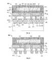
- FIGS. 1 and 2A microelectronic assembly 10 in accordance with an embodiment of the present invention for mounting a microelectronic element, such as a semiconductor chip, thereto is shown in FIGS. 1 and 2 .
- the assembly 10may include an interconnection substrate 12 having a top surface 13 and an opposing rear surface 15 .
- the substrate 12may contain a dielectric layer 16 having a top surface 14 facing the top surface 13 of the substrate 12 .
- the dielectric layer 16may have a thickness extending between the top surface 14 and the rear surface 15 of the substrate 12 in a direction perpendicular to the top surface 13 of about 100 to 1000 microns.
- the dielectric layer 16may have a rear surface that is at least partially coextensive with the rear surface 15 of the substrate 12 .
- the dielectric layer 16may be formed from epoxy, epoxy-based materials, such as epoxy-glass, polyimide-based materials or BT resin.
- the dielectric layer 16may have a Young's modulus of at least about 2 GPa, and most desirably about 6-10 GPa, and a coefficient of thermal of expansion of at least about 10 parts per million/° C.
- topAs used in this disclosure, terms such as “top”, “bottom”, “upward” or “upwardly” and “downward” or “downwardly” refer to the frame of reference of a microelectronic assembly, or an assembly or unit which incorporates such microelectronic assembly. These terms do not refer to the normal gravitational frame of reference.
- directionsare stated in this disclosure with reference to the “top” or “front” surface of the substrate 12 .
- directions referred to as “upward” or “rising from”shall refer to the direction orthogonal and away from the front surface 13 .
- Directions referred to as “downward”shall refer to the directions orthogonal to the front surface 13 and opposite the upward direction.
- a “vertical” directionshall refer to a direction orthogonal to the front surface.
- the term “above” a reference pointshall refer to a point upward of the reference point, and the term “below” a reference point shall refer to a point downward of the reference point.
- the “top” of any individual elementshall refer to the point or points of that element which extend furthest in the upward direction, and the term “bottom” of any element shall refer to the point or points of that element which extend furthest in the downward direction.
- the substrate 12may further include electrically conductive elements 17 disposed on the top surface 14 of the dielectric layer 16 .
- the conductive elements 17may include a conductive strip or trace 17 A exposed at the top surface 14 of the dielectric layer 16 and extending substantially parallel to the top surface 13 of the substrate, and a conductive leg 17 B electrically connected to the strip 17 A.
- the conductive elementsmay be formed from etchable conductive material, and typically are or consist essentially of metal including one or more metals selected from copper-based alloy, aluminum, nickel and gold.
- the conductive leg 17 Bmay extend from the strip 17 A, in a direction perpendicular to the direction that the strip 17 A extends, as a conductive via extending through openings 23 extending through the thickness of the dielectric layer 16 , to or adjacent to the rear surface 15 of the substrate.
- the conductive elementsmay provide for connections to other discrete components (not shown) arranged on or formed at least partially within the substrate 12 , or to external connections 54 , such as conductive material serving as a terminal formed at the rear surface 15 and electrically connected to the conductive leg 17 B.
- the conductive strip 17 Amay be an electrically conductive pad.
- an electrically conductive structureis “exposed at” a surface of a dielectric structure indicates that the electrically conductive structure is available for contact with a theoretical point moving in a direction perpendicular to the surface of the dielectric structure toward the surface of the dielectric structure from outside the dielectric structure.
- a terminal or other conductive structure which is exposed at a surface of a dielectric structuremay project from such surface; may be flush with such surface; or may be recessed relative to such surface and exposed through a hole or depression in the dielectric.
- a compliant dielectric layer 18may be disposed over the top surface 14 of the dielectric layer 16 .
- the compliant dielectric layer 18may have a height extending from a generally planar top surface 20 , which may form a portion of the top surface of the substrate, to an opposing generally planar bottom surface 22 , which faces the top surface 14 of the dielectric layer 16 , of about 10 to 50 microns.
- the compliant dielectric layer 18may be formed from a material having a relatively low elastic modulus, for example, a Young's modulus of less than about 2 GPa.
- the compliant dielectric layercan have elastic properties comparable to those of soft rubber about 20 to 70 Shore A durometer hardness.
- the compliant dielectric layermay be a dielectric, and have a material structure formed from materials having a density or hardness of a material used as a filler in compositions such as flexibilized epoxy, silicone, a low modulus epoxy, a TEFLON based material, a foam type material, a liquid-crystal polymer, a thermoset polymer, a fluoropolymer, a thermoplastic polymer, polyimide, polytetrafluoroethylene (PTFE), perfluoroalkoxy (PFA), fluorinated ethylene propylene (FEP) and polyfluoroethylene (PTFE) or like compositions.
- a material used as a filler in compositionssuch as flexibilized epoxy, silicone, a low modulus epoxy, a TEFLON based material, a foam type material, a liquid-crystal polymer, a thermoset polymer, a fluoropolymer, a thermoplastic polymer, polyimide, polytetrafluoroethylene (PTFE
- the compliant dielectric layer 18may be provided in the substrate 12 with the dielectric layer 16 as a dielectric element 6 in which the dielectric layer 16 has a Young's modulus that is at least 50% greater than the Young's modulus of the compliant dielectric layer 18 .
- the dielectric layer 16may have a material structure formed from materials having a density or hardness of a material used as a filler in compositions such as filled epoxy, epoxy glass, epoxy glass composite, glass woven material, ceramic or like materials.
- the layer 16may have a material structure different from the material structure of the compliant dielectric layer of the dielectric element 6 , the difference in the material structure being based on the difference between the density or hardness of a material used as a filler in the layer 16 and the density or hardness of a material used as a filler in the compliant dielectric layer 18 .
- a substrate of a microelectronic assembly containing the dielectric element 6may reduce mechanical stress between microelectronic elements, which are electrically connected to substrate contacts at a top surface of the substrate, and terminals at a rear surface of the substrate which are electrically connected to contacts of a microelectronic component external to the microelectronic assembly.
- the substratemay include a dielectric element having a first dielectric layer, such as the layer 18 , which is adjacent a first surface of the dielectric element at which microelectronic element contacts are to be joined, and a second dielectric layer, such as the layer 16 , which is between the first dielectric layer and a second surface of the dielectric element opposed to the first surface, where the second dielectric layer has a Young's modulus at least 50% greater than the Young's modulus of the first dielectric layer.
- the compliant dielectric layer 18can have openings extending through an entirety of the thickness of the layer 18 , through which portions of respective conductive strips 17 A are exposed.
- the openings 26may be substantially cone-shaped or cylindrically-shaped having substantially circularly-shaped top ends 30 at the top surface 20 of the compliant layer 18 and substantially circularly-shaped bottom ends 32 adjacent the conductive strips 17 A.
- the diameter or width of the top ends 30 of the openings 26may be about 30-40 microns, and the diameter or width of the bottom ends 32 of the openings 26 may be about 20-40 microns.
- the width of the bottom end of the opening 26can be smaller than the width at the top end; in another example, the bottom end width of the opening 26 can be the same as the top end width.
- the substrate 12may further include electrically conductive contacts 50 , such as contact pads, exposed at the top surface 20 of the compliant dielectric layer 18 .
- the substrate contacts 50overlie openings 26 formed over respective conductive strips 17 A, and may at least partially overlie portions of the compliant dielectric layer 18 adjacent the openings 26 .
- the contactsmay have a height in a direction perpendicular to the top surface 20 of the compliant layer of less than about 20 microns.
- Electrically conductive vias 60may extend from the substrate contacts 50 , into the openings 26 and through the entire thickness of the compliant dielectric layer 18 , to exposed portions of the conductive strips 17 A underlying the openings 26 , so as to electrically connect the conductive strips 17 A with respective substrate contacts 50 .
- the vias 60desirably are disposed entirely below the respective substrate contacts from which they extend, and fill the entirety of the openings 26 so as to have the same structure as the openings.
- An element 70such as a microelectronic element, for example, a semiconductor chip, having a generally planar rear face 72 and a generally planar front face 74 with electrical contacts or terminals 76 may be disposed on the substrate 12 .
- the chip 70may be mounted on the substrate 12 in a front-face-down orientation, with the front face 74 of the chip facing toward the top surface 20 of the compliant layer 18 .
- the electrical contacts 76may be electrically connected to internal electronic components (not shown) of the chip 70 .
- each of the electrical contacts 76may be associated with one of the contact pads 50 , and each of the contacts 76 is bonded to the associated contact pad by a mass 80 of electrically conductive material.
- the contacts 76 on the chip 70are electrically interconnected, via the masses 80 , the contact pads 50 and the conductive vias 60 , to the associated conductive strips 17 A underlying the compliant layer 18 .
- the masses 80may include a bond metal such as solder, which may or may not be lead-free, tin or indium.
- the dielectric element of the substratemay include one or more layers of compliant dielectric material and have conductive vias extending through a thickness of the one or more compliant dielectric layers, and one or more layers of rigid dielectric material and have conductive material, such as conductive legs or conductive vias, extending through a thickness of the one or more rigid layers, where substrate contacts are at a surface of a compliant dielectric layer of the dielectric element.
- the structural and material characteristics of the substrate contacts and the dielectric elementwhich includes a compliant dielectric layer adjacent the substrate contacts, a rigid layer and conductive elements between and extending through the rigid and compliant layers, may be adapted to permit displacement of the substrate contacts relative to the conductive elements, and provide that the displacement appreciably relieves mechanical stresses, such as may be caused by differential thermal expansion or contraction, which would be present in electrical connections between the substrate contacts and the microelectronic element absent such displacement.
- the structural and material characteristics of the substrate contacts, the conductive vias in the compliant layer and the compliant layermay be adapted to permit more movement of the substrate contacts relative to the associated conductive strips, in comparison to the amount of relative movement that would be permitted absent the combination of the compliant layer, the substrate contacts, and the conductive vias in the compliant layer adapted in accordance with the present invention, so as to appreciably reduce mechanical stresses in electrical connections between the associated contacts of the substrate and the chip.
- the term “movable”means that when the assembly is exposed to external loads, such as may occur as a result of thermal excursions during fabrication, testing or operation of the inventive assembly, the contacts are capable of being displaced relative to the conductive strips 17 A of the substrate, or terminals at the rear surface of the substrate, by the external loads applied to the substrate contacts through the joints with the contacts of the microelectronic element, to the extent that the displacement appreciably relieves mechanical stresses, such as those caused by differential thermal expansion which would be present in the electrical connections between the microelectronic element and the substrate absent such displacement.
- the contacti.e., contact pad 50
- the associated conductive via 60may be displaced from a normal position (shown in solid lines) to a displaced position (shown in dashed lines), based on deformation of the compliant layer 18 (also shown in dashed lines), such as may be caused by differential thermal expansion or contraction occurring during operation, fabrication or testing of the assembly 10 .
- the amount of movement of the contact pad 50 that is permittedmay depend on a diameter A of the contact pad, which is measured in a direction along the top surface 20 of the compliant layer; the diameter B of the surface portion of the conductive via 60 exposed and coupled to the contact pad 50 , where such surface portion desirably has the same configuration as the top end 30 of the opening 26 ; the Young's modulus of the compliant layer; and the height of the conductive via.
- the capability of the contact pad to movemay increase with decreasing ratio of B to A, and the ratio of B to A desirably is at least less than about 40%.
- the capability of the contact pad to movemay increase with decreasing Young's modulus of the compliant layer in relation to the Young's moduli of the rigid dielectric layer and the chip, and the Young's modulus of the compliant layer desirably may be less than about 2 GPa. Further, the capability of the contact pad to move may increase with increasing height of the conductive pad, and desirably the height is at least 20 microns.
- the contact pad 50 and the conductive via 60may be displaced to the positions indicated by broken lines 50 A and 60 A, respectively, when the substrate 12 with the compliant layer 18 , the rigid layer 16 and the conductive strip 17 A expand in the direction of arrow D to the positions indicated by broken lines 18 A, 16 A and 17 A′.
- This displacementis permitted by the flexibility of the compliant layer 18 , which may flex and deform at the top surface 20 to obtain an approximated deformed condition indicated by broken lines 20 A.
- the compliant layer 18has more compliance than the pad 50 and the conductive via 60 , the layer 18 does not substantially resist flexing based on mechanical stresses applied at the contact pads 50 resulting from the differential expansion or contraction of the dielectric element 6 of the substrate and the chip.
- the compliant layermay expand in the direction of the arrow E at a side 51 of the contact pad 50 facing the direction in which the expansion is occurring, and compress in the direction of the arrow F at a side 53 of the contact pad 50 opposite the side 51 .
- the conductive padmay also move in other directions, such as opposite to the directions E and F at the opposing sides 51 and 53 when a contraction occurs in a direction opposite to the direction D, and also in directions perpendicular to these directions, into and out of the plane of the drawing as seen in FIG. 3 .
- the compliant layermay flex to accommodate movement of the contact pad 50 relative to the conductive strip 17 A, without deformation of the contact pad, thereby avoiding damage to the contact pad when the assembly is exposed to differential thermal conditions, such as during fabrication, operation or testing of the assembly.
- the dielectric layer 16may have a coefficient of thermal expansion substantially greater than a coefficient of thermal expansion of the microelectronic element, such that the microelectronic element applies substantial loads to the substrate contacts due to the difference in the coefficients of thermal expansion between the dielectric layer 16 and the microelectronic element.
- the compliant layermay permit displacement to reduce mechanical stress in the electrical connections between the substrate contacts and the microelectronic element to a degree that is appreciably less than the mechanical stress that would be present in electrical connections between the substrate contacts and the microelectronic element absent such displacement.
- the electrical connectionssuch as solder, are subject to fatigue failure due to stresses.
- a substantial reduction in the stress applied to the electrical connectionsmay be 25%.
- about a 50% reduction in the stress applied to the electrical connectionsmay be achieved.
- the compliant layermay permit displacement to appreciably relieve the aforementioned mechanical stresses for temperatures of the assembly and its parts ranging from about ⁇ 55° C. to 125° C.
- the assembly 10may be fabricated by a process as schematically illustrated in FIGS. 4A-4C .
- FIGS. 4A-4Ca portion of a single region of the microelectronic assembly 10 showing interconnection of the chip contact with an associated substrate contact is shown in the drawings FIGS. 4A-4C .
- fabrication processing of the assembly 10is described below with respect to a single contact between the chip and substrate, it is to be understood that the same fabrication processing occurs in the other regions of the assembly 10 to connect chip contacts to associated contact pads on the substrate.
- a semiconductor substrate 12may be provided including a rigid dielectric layer 16 , a conductive strip or trace 17 A formed at a top surface 14 of the rigid layer 16 and a conductive leg or via 17 B formed to extend from the strip 17 A, through a hole 23 extending through the entirety of thickness of the rigid layer 16 , to a rear surface 15 of the substrate, where the conductive elements 17 are formed using conventional masking and etching techniques.
- a compliant dielectric layer 18may be joined to the substrate to overlie the top surface 14 of rigid layer 16 , such as by thin film deposition, silk-screening or using an adhesive (not shown).
- the adhesivecan be any suitable material, and can be epoxy.
- the adhesiveshould have properties and a glass transition temperature T g sufficiently high to withstand the maximum heating to be encountered during subsequent thermal processing and operation.
- the adhesivemay cover exposed portions of the top surfaces of the dielectric element and conductive strip 17 A.
- the adhesiveis homogeneously applied by spin bonding, as described in U.S. Pat. Nos. 5,980,663 and 6,646,289, the disclosures of which are incorporated herein by reference.
- any other suitable techniquemay be employed.
- an oxide/nitride layermay be used to join the compliant layer 18 to the substrate 12 .
- an opening 26may be formed extending through the entirety of the thickness of the compliant layer 18 , and any optional adhesive layer, at a position overlying a conductive strip 17 A, using conventional masking and etching processes, so as to expose the conductive strip 17 A.
- photolithographymay be used to form mask patterns (not shown) overlying the front surface of the compliant layer 18 , after which the layer 18 may be etched from the front surface 20 using wet or dry etching.
- the opening 26may be formed by laser ablation of the compliant layer 18 .
- a directed stream of particlescan form openings 26 in the compliant layer 18 , such as disclosed in commonly owned co-pending U.S. application Ser. No. 12/842,612 filed Jul. 23, 2010, incorporated by reference herein.
- Conductive materialmay then be deposited into, and so as to fill, the opening 26 to form the conductive via 60 .
- masking and photolithographymay be used to deposit the same conductive material used to form the conductive via, to form a contact pad 50 overlying the conductive via, after the opening 26 becomes filled with the conductive material.
- the contact pad 50optionally may be formed to overlie a portion of the top surface 20 of the compliant layer 18 adjacent the opening 26 in which the conductive via 60 is formed, as shown in FIG. 4B .
- a contact padmay be formed so that the associated conductive via underlying the contact pad extends from a substantially central region of a surface of the contact pad facing the conductive via.
- a metal layermay be selectively formed on an exposed surface of the conductive via at the top surface of the compliant layer, and also on an exposed surface portion of the compliant layer 18 adjacent the conductive via, to form the contact pad 50 .
- the metal layermay be formed by sputtering or blanket metallization, and followed by surface patterning using photolithography. See U.S. Patent Publication No. 2008-0116544, filed Nov. 22, 2006, incorporated by reference herein.
- the metal layermay be formed by electroless plating.
- a masking dielectric layer(not shown) may be formed patterned on the exposed surface of the compliant layer to define the contact pads 50 .
- the substrate 12 including the rigid layer 16 , the conductive elements 17 , the compliant dielectric layer 18 , the conductive vias 26 and the contact pads 50may be formed by one or more of the processes described in U.S. application Ser. No. 13/105,325 filed May 11, 2011 and U.S. application Ser. No. 13/155,552 filed Jun. 8, 2011, which are incorporated by reference herein.
- a solder bump 80may be formed on the contact pad 50 to electrically interconnect the contact pad 50 with a conductive pad 76 on a front surface 74 of the chip 70 , which is disposed overlying the substrate and mounted to the substrate using conventional techniques.
- the chip 70may include a dielectric region 100 disposed between the surface 74 and a semiconductor region 102 which may embody active circuit elements.
- the dielectric region 100may be an “extremely low dielectric (”ELK′′) constant ‘k’” or “ultralow dielectric constant ‘k’” (“ULK”) material having a specific material or including a multiplicity of “pores,” i.e., voids dispersed throughout the dielectric region 100 .
- the region 100may have a porosity greater than 20%, 40% or 60% determined as a ratio of the combined volume of all the voids relative to the volume enclosed by exterior surfaces of the dielectric region.
- the low dielectric constantcan be achieved by the chip having substantial porosity, and porosity can cause the material to be relatively fragile.
- the structure and Young's modulus of the compliant layer, and the structure of the conductive vias and the conductive padsmay be adapted to have a reduced stiffness in accordance with the ELK characteristics of the dielectric region of the chip, so as to reduce an amount of stress transferred to the dielectric region to below a level which the ELK region can tolerate, and thereby avoid the dielectric region becoming damaged during expansion or contraction of the dielectric element relative to the microelectronic element.
- the element 70 of the microelectronic assembly 10may have a coefficient of thermal expansion that is less than 10 parts per million/° C. and consist essentially of dielectric material.
- the element 70may include glass or ceramic materials.
- the element 70may include a plurality of passive components, such as resistors, capacitors or inductors, in any combination, or be a passive chip of semiconductor material.
- a microelectronic assembly 200may have a substantially similar construction as the assembly 10 of FIG. 2 , except that substantially rigid conductive posts 204 may extend above the compliant layer from exposed surfaces 58 of the contact pads 50 that confront the surface 74 of the chip 70 .
- the posts 204may consist essentially of copper, and can be formed by plating or etching or a combination thereof.
- the posts 204may extend from a bottom surface 206 , which faces the exposed surface 58 of the pads 50 , above the compliant layer 18 to a top surface 208 adjacent the surface 74 of the chip 70 .
- the postmay have an edge surface extending from the base 206 adjacent pad 206 to an end surface or top surface 208 remote from the base.
- the post 204may include opposing edge surfaces 210 extending from the surface 206 toward each other and terminating at the top surface 208 .
- the height of the post 204 extending between the top surface 208 and the bottom surface 206 , in a direction perpendicular to the surface of the compliant layer 18 ,may be about 10-100 microns.
- the postmay have a height at least half the distance of the bottom surface 206 extending in directions along the top surface of the compliant layer.
- the bond metal 80desirably may contact the top surface and edge surfaces of the post, and optionally a portion of the exposed surface 58 of the contact pad 50 .
- a microelectronic assembly 250may have a substantially similar construction as the assembly 200 of FIG. 5 , except that the bond metal 80 may contact the top surface and edge surfaces of the posts but not contact the contact pad 50 .
- a microelectronic assembly 300may have a substantially similar construction as the assembly 200 of FIG. 5 , except that substantially rigid conductive posts 304 extend from exposed surfaces of the conductive vias 60 , and exposed portions of the surface 20 of the compliant layer 18 , facing the surface 74 of the chip.
- the posts 304may have a square or rectangular shape with a top surface 306 adjacent the chip and a bottom surface 308 opposing the top surface 306 .
- the bottom surface 308may overlie the exposed surface of the associated conductive via 60 and also portions of the top surface of the compliant layer adjacent the associated conductive via.
- the bond metal 80may contact only the top surface and the edge surfaces of the post 304 .
- the posts 304may have a height extending between the top and bottom surfaces 306 , 308 , perpendicular to the surface 20 of the compliant layer 18 , of about 20-100 microns.
- a microelectronic assembly 400may include a substrate 412 , which is fabricated and has features similar to the substrate of the assembly 10 of FIG. 2 . Like reference numerals are used in this embodiment to designate the same or similar components as previously discussed.
- a metal layermay be selectively provided on uncovered portions of the top surface 20 of the compliant dielectric layer 18 and on exposed top surfaces 430 of the conductive vias 60 to obtain conductive portions 450 .
- the portions 450may include contacts 450 A adjacent the conductive vias 60 , and traces 450 B extending along the top surface 20 of the layer 18 from the contacts 450 A that may electrically connect the contacts 450 A with other conductive elements within or attached to the substrate 412 .
- the conductive vias 17 Bmay have a construction similar to the conductive vias 60 , and also some of the vias 17 B may be vertically aligned with the vias 60 .
- the substrate 412may include conductive portions 470 formed at exposed portions of bottom surfaces 414 of the conductive vias 17 B, and uncovered portions of bottom surfaces 416 of the rigid layer 16 which extend from the exposed portions of the bottom surfaces 414 .
- the conductive portions 470may be formed at uncovered portions of the bottom surface 416 of the rigid layer that do not extend from the exposed portions of the bottom surfaces 414 .
- the conductive portions 470may be formed selectively from a layer of metal, using similar techniques as described above to obtain the conductive traces 17 A. Some of the conductive portions 470 may be electrically connected with, and optionally extend from, bottom surfaces 414 of the conductive vias 17 B.
- masses 474 of electrically conductive materialmay be provided on exposed portions of bottom surfaces 472 of the conductive portions 470 .
- the masses 474may be obtained, for example, by patterning a solder resist layer on the uncovered portions of the bottom surface 416 of the rigid layer 16 , forming conductive material on exposed portions of the surfaces 472 , and then removal of the solder resist layer.
- the masses 474may be electrically interconnected with the conductive portions 450 through the conductive portions 470 , which may include contacts that serve as terminals of the substrate 412 , the conductive vias 17 B, the traces 17 A and the conductive vias 60 .
- the conductive portions 470may serve as the terminals of the substrate 412 , and partially overlie and be in contact with the conductive vias 17 B.
- the masses 474may include a bond metal such as solder, which may or may not be lead-free, or such as tin or indium.
- the microelectronic assembly 400may incorporate a microelectronic element 502 , such as a semiconductor chip, having a generally planar front face 504 , a generally planar rear face 507 and contacts (not shown) exposed at the front face 504 .
- the substrate 412 and the chip 502may be assembled with the chip 502 mounted on the substrate 412 in a front-face-down orientation, with the front face 504 of the chip facing top surface 451 of the conductive portions 450 .
- the contacts on the chip 502may be electrically connected to internal electronic components (not shown) of the chip 502 .
- the contacts on the surface 504 of the chipmay be aligned and bonded with conductive material of the substrate, such as the contacts 450 A, or a contact (not shown) on an optional protective layer 468 formed on the upper surfaces 451 of the conductive portions 450 , by masses 506 of electrically conductive material.
- the masses 506may include a bond metal such as solder, which may or may not be lead-free, or such as tin or indium.
- the protective layer 468may include a corrosion-resistant or oxidation-resistant metal, such as nickel or gold, or be formed from organic solderability preservative (“OSP”) or a flux material.
- OSPorganic solderability preservative
- etch-resistant material used to form the portions 450may also include a corrosion-resistant metal, such as nickel or gold, such that the material may be left in place as the layer 468 after formation of the portions 450 .
- the traces 450 Bmay extend along the surface 20 of the compliant layer 18 away from the contacts 450 A and electrically connect the contacts 450 A with the conductive vias 60 , which extend downwardly from the traces 450 B.
- the traces 450 Bmay partially overlie and be in contact with the conductive vias 60 , such that the traces 450 B electrically connect the contacts 450 A with the vias 60 .
- the vias 60may be electrically connected with the vias 17 B through the traces 17 A, from which the vias 60 and 17 B may extend.
- the conductive portions 470may be electrically connected with the contacts 450 A, which are joined to the contacts on the chip 502 by the masses 506 , by a conductive structure including the conductive vias 60 and 17 B and the traces 17 A.
- the conductive portions 470which are electrically connected with the vias 17 B, serve as terminals that may provide for electrical connection of the vias 60 , through the traces 17 B and the vias 17 B, with contacts (not shown) of an external microelectronic element 570 , through the solder masses 474 formed on the outer surfaces 472 of the portions 470 .
- a dielectric element 480 in the substrate 412may include the compliant dielectric layer 18 adjacent the chip 502 in combination with the rigid layer 16 .
- a conductive structure electrically connecting terminals with substrate contactsmay include conductive traces, such as the traces 450 B, extending along and parallel to a front surface 481 A of the dielectric element 480 , such as the surface 20 of the compliant layer 18 ; conductive portions, such as the contacts 470 , extending along and parallel to a bottom surface 481 B of the dielectric element 480 , such as the surface 416 of the rigid layer 16 ; and conductive traces between the surfaces 481 A and 481 B and, in one example, extending along a boundary between the layers 16 and 18 , such as the traces 17 A between the layers 16 and 18 .
- a microelectronic packagemay be formed by using the terminals 470 to bond the assembly 400 to corresponding contacts of the external microelectronic element 570 , which may be a circuit panel included in electronic devices such as a smart phone, mobile phone, personal digital assistant (PDA) and the like, with bonding material, such as solder, between the terminals and the circuit panel that joins the assembly 400 with the circuit panel.
- the bonding materialmay be the solder masses 474 of the assembly 400 .
- the solder masses 474may be omitted from the assembly 400 , and bonding material, such as solder, may be applied at the terminals 470 when the assembly 400 is joined to the external microelectronic element 570 .
- the dielectric element 480may include a compliant dielectric sub-element adjacent to the top surface of the substrate, where the compliant dielectric sub-element is formed from a plurality of adjacent layers of compliant dielectric material with conductive traces in between the adjacent layers, and has conductive vias extending through a thickness of the compliant dielectric layers, such as disclosed in U.S. application Ser. No. 13/105,325 filed May 11, 2011 incorporated by reference herein.
- the dielectric element 480may include a rigid dielectric sub-element between the compliant dielectric layer adjacent to the top surface of the substrate and the rear surface of the substrate, where the rigid dielectric sub-element is formed from a plurality of adjacent layers of rigid dielectric material with conductive traces in between the adjacent layers, and has conductive vias extending through a thickness of the rigid dielectric layers.
- the assembly 400further may include a rigid underfill 510 between the surface 504 of the chip 502 and the top surface 20 of the compliant layer 18 facing the chip.
- the rigid underfill 510may be formed adhered to portions of the surface 20 , exposed portions of the conductive portions 450 and exposed portions of the optional protective layer 468 .
- the rigid underfill 510may overlie portions of the surface 20 of the compliant dielectric layer 18 adjacent to the chip 502 .
- the rigid underfill 510may have a Young's modulus of about 6 GPa or greater and include dielectric material.
- a layer of encapsulant 514may be provided covering portions of the substrate, and portions of the chip and the underfill, to protect the encapsulated components from the external environment.
- the encapsulant 514may include dielectric material, and may or may not be molded, such as shown in FIG. 8 .
- underfill and a layer of encapsulantmay be made of the same material, such as a dielectric material, and applied at the same time, such as part of a molding process.
- the structural and material characteristics of the substrate contacts, the terminals and a dielectric elementwhich includes a compliant dielectric layer adjacent the substrate contacts and a rigid layer as exemplified in the assembly 400 , may be adapted to permit displacement of the substrate contacts relative to the terminals of the substrate, and provide that the displacement appreciably relieves mechanical stresses, such as may be caused by differential thermal expansion or contraction, which would be present in electrical connections between the substrate contacts and a microelectronic element connected with the terminals absent such displacement.
- the structural and material characteristics of the substrate contacts, the dielectric element and the terminalsmay be adapted to permit more movement of the substrate contacts relative to the terminals, in comparison to the amount of relative movement that would be permitted absent the combination of the dielectric element between the substrate contacts and the terminals, the substrate contacts and the terminals adapted in accordance with the present invention.
- the movability of the substrate contacts under applied loadsmay appreciably reduce mechanical stresses in the electrical connections between the substrate contacts and the contacts of the chip attached thereto.
- the contacts 450 Adesirably can move or tilt slightly with respect to the solder masses 472 , which may be bonded to the conductive regions 470 that serve as terminals of the substrate 412 , and the conductive regions 470 serving as the terminals, based on the compliancy of the dielectric element 480 between the conductive regions 450 and the conductive regions 470 .
- the dielectric element 480can flex or otherwise deform to accommodate movement of the contacts 450 A bonded to the chip relative to the terminals 470 , when the terminals 470 are attached to an external component, as may be caused, for example, by differential thermal expansion and contraction of the elements during operation, during manufacture as, for example, during a solder bonding process, or during testing.
- a solder resist layer 490may overlie portions of the surface 416 of the rigid layer 16 except for locations at which the terminals 470 are formed.
- the terminals 470may be adapted to simultaneously carry different electrical signals or electrical potentials, and be bonded to an external component 570 similarly as in FIG. 8 .
- the substrate 412 of FIG. 8may be joined to a plurality of microelectronic elements 502 by masses of a conductive material such as a bond metal, e.g., solder, tin or indium, or a conductive paste 506 , which electrically interconnects and bonds contacts (not shown) of the elements 502 with the pads 450 A.
- a conductive materialsuch as a bond metal, e.g., solder, tin or indium, or a conductive paste 506 , which electrically interconnects and bonds contacts (not shown) of the elements 502 with the pads 450 A.
- the underfill 110may be applied between each of the elements 502 and the substrate, followed by application of the encapsulant.
- the substrate 412 covered by the encapsulantmay then be severed to obtain discrete microelectronic assemblies 400 each containing a microelectronic element 502 , and the conductive layer 469 may be etched to form conductive portions 470 , which serve as terminals, or alternatively pads, of each of the discrete microelectronic assemblies 400 .
- a microelectronic assembly 500has features similar to that shown in FIG. 8 , except that the conductive portions 470 are shaped in the form of posts, the posts serving as terminals of the substrate to which an external chip may be connected.
- the terminals 470may have a thickness of about 50-300 ⁇ m.
- the terminals 470have horizontal dimensions (in directions parallel to surfaces of the dielectric element 480 ) at a surface adjacent the rigid layer 16 greater than the horizontal dimensions at a surface remote from the layer 16 , such that the horizontal dimensions of the terminal 470 decrease in the direction away from the layer 16 so as to be in the form of a post, which desirably is a substantially rigid solid metal post.
- some of the conductive portions 470may be aligned with the conductive vias 17 B, which electrically connect the conductive portions 470 that serve as the terminals of the substrate with the conductive portions 450 , through the traces 17 A and the conductive vias 60 .
- one or more solder masses 474may be formed on the exposed surfaces of the terminals 470 of the assembly 500 .
- a microelectronic assembly 600may include the chip 502 electrically connected with a substrate 612 , which is fabricated and has features similar to the substrate of the assembly 400 of FIG. 8 .
- the substrate 612can be similar to the substrate 412 , except that the structure of a dielectric element 680 includes the compliant dielectric layer 18 adjacent the substrate contacts, the rigid layer 16 and an additional compliant dielectric layer 618 having top and bottom surfaces 620 , 622 , where the layer 16 is between the layers 18 and 618 .
- the compliant dielectric layer 618may desirably have a Young's modulus of less than about 2 GPa, and the rigid layer 16 may have a Young's modulus at least 50% greater than the Young's modulus of the layer 618 .
- additional conductive traces 630may be disposed between the top surface 620 of the compliant layer 618 and the bottom surface 416 of the rigid layer 16 and extend in a lateral direction parallel to the surfaces 620 and 416 .
- additional conductive vias 660may extend through holes in the compliant layer 618 and electrically connect the traces 630 with the terminals 470 .
- the traces 630may electrically connect the vias 17 B with the vias 660 , such that the terminals 470 are electrically connected with the contacts 450 A through a conductive structure including the vias 660 , the traces 630 , the vias 17 B, the traces 17 A and the vias 60 .
- fabricationmay be performed to laminate conductive layer 632 , from which the traces 630 are formed, to the surface 416 of the rigid layer 16 or the top surface 620 of the compliant layer 618 , so that projections 619 of dielectric material of the dielectric material of the layer 618 extend from the surface 620 upwardly through openings between the conductive portions 630 of the layer 632 .
- a conductive layer 469 from which the conductive portions 470 are formedmay be laminated to the bottom surface 622 of the layer 618 during fabrication. Further, the layer 618 may be patterned with holes that contain the vias 660 in a pattern corresponding to the holes of the rigid layer 16 , such that the vias 660 and 17 B are vertically aligned and the vias 660 and 17 B extend from the traces 630 .
- the terminals 470are electrically connected with the contacts 450 through the vias 660 , the traces 630 , the vias 17 B, the traces 17 A and the vias 60 , such that the terminals 470 may bend slightly due to the compliancy of the dielectric element 680 , to accommodate movement relative to the contacts 450 A connected to the chip 502 that may be caused by differential thermal expansion and contraction.
- a microelectronic assembly 700has features similar to that shown in FIG. 10 , except that the terminals are conductive portions 470 at the surface 622 of the compliant layer 618 which are in the shape of posts, similarly as in the assembly shown in FIG. 9 .
- the assemblies of FIGS. 10-11may include a solder resist layer overlying the surface 622 of the compliant layer 618 , such as described above with reference to FIG. 8 .
- a system 800 in accordance with a further embodiment of the inventionincludes a microelectronic assembly 806 as described above in conjunction with other electronic components 808 and 810 .
- component 808is a semiconductor chip whereas component 810 is a display screen, but any other components can be used.
- the systemmay include any number of such components.
- the microelectronic assembly 806may be any of the assemblies described above. In a further variant, any number of such microelectronic assemblies may be used.
- Microelectronic assembly 806 and components 808 and 810are mounted in a common housing 811 , schematically depicted in broken lines, and are electrically interconnected with one another as necessary to form the desired circuit.
- the systemincludes a circuit panel 812 such as a flexible printed circuit board, and the circuit panel includes numerous conductors 814 , of which only one is depicted in FIG. 12 , interconnecting the components with one another.
- the housing 811is depicted as a portable housing of the type usable, for example, in a cellular telephone or personal digital assistant, and screen 810 is exposed at the surface of the housing.
- structure 806includes a light sensitive element such as an imaging chip
- a lens 816 or other optical devicealso may be provided for routing light to the structure.
- FIG. 12the simplified system shown in FIG. 12 is merely exemplary; other systems, including systems commonly regarded as fixed structures, such as desktop computers, routers and the like can be made using the structures discussed above.
Landscapes
- Engineering & Computer Science (AREA)
- Microelectronics & Electronic Packaging (AREA)
- Computer Hardware Design (AREA)
- Power Engineering (AREA)
- Physics & Mathematics (AREA)
- Condensed Matter Physics & Semiconductors (AREA)
- General Physics & Mathematics (AREA)
- Manufacturing & Machinery (AREA)
- Ceramic Engineering (AREA)
- Mechanical Engineering (AREA)
- Wire Bonding (AREA)
- Internal Circuitry In Semiconductor Integrated Circuit Devices (AREA)
Abstract
Description
- This application claims benefit of the filing date of U.S. Provisional Patent Application No. 61/425,432, filed Dec. 21, 2010, the disclosure of which is hereby incorporated herein by reference.
- The subject matter shown and described in the present application relates to assemblies incorporating semiconductor chips and to methods and components useful in making such assemblies.
- Modern electronic devices utilize semiconductor chips, commonly referred to as “integrated circuits” which incorporate numerous electronic elements. These chips are mounted on substrates which physically support the chips and electrically interconnect each chip with other elements of the circuit. The substrate may be a part of a discrete chip package or microelectronic assembly used to hold a single chip and equipped with terminals for interconnection to external circuit elements. Such substrates may be secured to an external circuit board or chassis. Alternatively, in a so-called “hybrid circuit” one or more chips are mounted directly to a substrate forming a circuit panel arranged to interconnect the chips and the other circuit elements mounted to the substrate. In either case, the chip must be securely held on the substrate and must be provided with reliable electrical interconnection to the substrate.
- In a microelectronic assembly, structures electrically interconnecting a chip to a substrate ordinarily are subject to substantial strain caused by thermal excursions or cycling between low and high temperatures as temperatures within the device change, such as may occur during fabrication, operation or testing of the device. For example, during operation, the electrical power dissipated within the chip tends to heat the chip and substrate, so that the temperatures of the chip and substrate rise each time the device is turned on and fall each time the device is turned off. As the chip and the substrate ordinarily are formed from different materials having different coefficients of thermal expansion, the chip and substrate ordinarily expand and contract by different amounts. This causes electrical contacts on the chip to move relative to electrical contact pads on the substrate as the temperature of the chip and the substrate changes. This relative movement can deform electrical interconnections between the chip and substrate and places them under mechanical stress. These stresses are applied repeatedly with repeated operation of the device, and can cause breakage of the electrical interconnections, which in turn reduces reliability performance of the device. Thermal cycling stresses may occur even where the chip and substrate are formed from like materials having similar coefficients of thermal expansion, because the temperature of the chip may increase more rapidly than the temperature of the substrate when power is first applied to the chip.
- Improvements can be made to structures that provide for electrical interconnection of a chip to a substrate of a microelectronic assembly and the processes used to fabricate such structures.
- In accordance with one embodiment of the invention, a microelectronic assembly may include a microelectronic element having a plurality of contacts exposed at a face thereof, and a substrate. The substrate may include a first dielectric layer having electrically conductive elements thereon and a coefficient of thermal expansion of at least 10 parts per million/° C.; and a second dielectric layer overlying the first dielectric layer, having a surface confronting the face of the microelectronic element, and having a Young's modulus of less than about 2 GPa. In addition, the substrate may include a plurality of electrically conductive substrate contacts exposed at the surface and respectively overlying the conductive elements. Further, the substrate may include a plurality of conductive vias extending through the second dielectric layer. The conductive vias may electrically connect the conductive elements with the respective substrate contacts and be disposed entirely below the respective substrate contacts. Further, the substrate contacts may be joined respectively to the contacts of the microelectronic element.
- In accordance with another embodiment of the invention, a method for forming a microelectronic assembly may include providing a substrate including a first dielectric layer having a first composition having electrically conductive elements thereon, the first dielectric layer having a coefficient of thermal expansion of at least10 parts per million/° C.; forming a second dielectric layer overlying the first dielectric layer having a surface at which electrically conductive substrate contacts respectively overlying the conductive elements are exposed, the second dielectric layer having a Young's modulus of less than about 2 GPa; electrically connecting the conductive elements respectively with the substrate contacts by conductive vias extending through the second dielectric layer, the vias being disposed entirely below the respective substrate contacts; and joining the substrate contacts to respective contacts exposed at a face of a microelectronic element, the surface of the substrate confronting the face of the microelectronic element.
- In accordance with a further embodiment of the invention, a microelectronic assembly may include an element having a coefficient of thermal expansion less than 10 parts per million/4° C. and a plurality of contacts exposed at a face thereof, and a substrate. The substrate may include a first dielectric layer having a first composition having electrically conductive elements thereon, the first dielectric layer having a coefficient of thermal expansion of at least 10 parts per million/° C.; a second dielectric layer overlying the first dielectric layer and having a surface confronting the face of the microelectronic element, the substrate having a plurality of electrically conductive substrate contacts exposed at the surface and respectively overlying the conductive elements, and the second dielectric layer having a Young's modulus of less than about 2 GPa; and a plurality of conductive vias extending through the second dielectric layer, electrically connecting the conductive elements with the respective substrate contacts and being disposed entirely below the respective substrate contacts. Further, the substrate contacts may be joined respectively to the contacts of the microelectronic element.
- In accordance with another embodiment of the invention, a microelectronic assembly may include a substrate. The substrate may include a dielectric element having first and second opposed surfaces, a first dielectric layer having a first material structure adjacent the first surface, and a second dielectric layer having a second material structure different from the first material structure. The second dielectric layer may be disposed between the first dielectric layer and the second surface, the first dielectric layer may have a Young's modulus less than two gigapascal (GPa), and a Young's modulus of the second dielectric layer may be at least 50% greater than the Young's modulus of the first dielectric layer. The substrate further may include a plurality of substrate contacts at the first surface; a plurality of terminals at the second surface; and a conductive structure extending through the first and second dielectric layers and electrically connecting the substrate contacts with the terminals. The assembly may further include a microelectronic element having a face confronting the first surface and a plurality of element contacts thereon joined with the substrate contacts through conductive masses; and a rigid underfill between the face of the microelectronic element and the first surface. Further, the terminals may be usable for bonding the microelectronic assembly to corresponding contacts of a component external to the microelectronic assembly.
- In accordance with another embodiment of the invention, a microelectronic assembly may include a substrate, and the substrate may include a dielectric element having first and second opposed surfaces, a first dielectric layer having a first material structure adjacent the first surface and a second dielectric layer having a second material structure different from the first material structure. The second dielectric layer may be disposed between the first dielectric layer and the second surface, the first dielectric layer may have a Young's modulus less than two gigapascal (GPa), and a Young's modulus of the second dielectric layer may be at least 50% greater than the Young's modulus of the first dielectric layer. The substrate may further include a plurality of substrate contacts at the first surface; a plurality of terminals at the second surface; and a conductive structure extending through the first and second dielectric layers and electrically connecting the substrate contacts with the terminals. The assembly may further include a microelectronic element having a face confronting the first surface and a plurality of element contacts thereon joined with the substrate contacts through conductive masses; and a rigid underfill between the face of the microelectronic element and the first surface. Further, the terminals may be usable for bonding the microelectronic assembly to corresponding contacts of a component external to the microelectronic assembly such that the substrate contacts are movable with respect to the terminals.
- In accordance with another embodiment of the invention, a method of fabricating a microelectronic assembly may include joining element contacts at a face of a microelectronic element with a plurality of substrate contacts at a first surface of a dielectric element of a substrate confronting the face through conductive masses. The dielectric element may have a conductive element at a second surface opposed to the first surface, a first dielectric layer having a first material structure adjacent the first surface, and a second dielectric layer having a second material structure different from the first material structure. The second dielectric layer may be disposed between the first dielectric layer and the second surface, the first dielectric layer may have a Young's modulus less than two gigapascal (GPa), a Young's modulus of the second dielectric layer may be at least 50% greater than the Young's modulus of the first dielectric layer, and the substrate may include a conductive structure extending through the first and second dielectric layers. The method may further include forming a rigid underfill between the face of the microelectronic element and the first surface of the dielectric element; and patterning the conductive element after the joining step to form terminals at the second surface of the dielectric element. The substrate contacts may be electrically connected with the terminals through the conductive structure, and the terminals may be usable to electrically connect the microelectronic assembly to a component external to the microelectronic assembly.
FIG. 1 is a diagrammatic perspective view of a microelectronic assembly, in accordance with one embodiment of the invention.FIG. 2 is a fragmentary sectional view taken along line2-2 inFIG. 1 .FIG. 3 is fragmentary view, on an enlarged scale, of a portion of the microelectronic assembly shown inFIG. 2 FIGS. 4A-4C are sectional views illustrating stages in a method of fabricating a microelectronic assembly, in accordance with an embodiment of the invention.FIG. 5 is a fragmentary sectional view of a microelectronic assembly, in accordance with another embodiment of the invention.FIG. 6 is a fragmentary sectional view of a microelectronic assembly, in accordance with another embodiment of the invention.FIG. 7 is a fragmentary sectional view of a microelectronic assembly, in accordance with another embodiment of the invention.FIG. 8 is a fragmentary sectional view of a microelectronic assembly, in accordance with another embodiment of the invention.FIG. 9 is a fragmentary sectional view of a microelectronic assembly, in accordance with another embodiment of the invention.FIG. 10 is a fragmentary sectional view of a microelectronic assembly, in accordance with another embodiment of the invention.FIG. 11 is a fragmentary sectional view of a microelectronic assembly, in accordance with another embodiment of the invention.FIG. 12 is a schematic depiction of a system according to one embodiment of the invention.- A
microelectronic assembly 10 in accordance with an embodiment of the present invention for mounting a microelectronic element, such as a semiconductor chip, thereto is shown inFIGS. 1 and 2 . Theassembly 10 may include aninterconnection substrate 12 having atop surface 13 and an opposingrear surface 15. Thesubstrate 12 may contain adielectric layer 16 having atop surface 14 facing thetop surface 13 of thesubstrate 12. Thedielectric layer 16 may have a thickness extending between thetop surface 14 and therear surface 15 of thesubstrate 12 in a direction perpendicular to thetop surface 13 of about 100 to 1000 microns. In one embodiment, thedielectric layer 16 may have a rear surface that is at least partially coextensive with therear surface 15 of thesubstrate 12. Thedielectric layer 16 may be formed from epoxy, epoxy-based materials, such as epoxy-glass, polyimide-based materials or BT resin. In addition, thedielectric layer 16 may have a Young's modulus of at least about 2 GPa, and most desirably about 6-10 GPa, and a coefficient of thermal of expansion of at least about 10 parts per million/° C. - As used in this disclosure, terms such as “top”, “bottom”, “upward” or “upwardly” and “downward” or “downwardly” refer to the frame of reference of a microelectronic assembly, or an assembly or unit which incorporates such microelectronic assembly. These terms do not refer to the normal gravitational frame of reference. For ease of reference, directions are stated in this disclosure with reference to the “top” or “front” surface of the
substrate 12. Generally, directions referred to as “upward” or “rising from” shall refer to the direction orthogonal and away from thefront surface 13. Directions referred to as “downward” shall refer to the directions orthogonal to thefront surface 13 and opposite the upward direction. A “vertical” direction shall refer to a direction orthogonal to the front surface. The term “above” a reference point shall refer to a point upward of the reference point, and the term “below” a reference point shall refer to a point downward of the reference point. The “top” of any individual element shall refer to the point or points of that element which extend furthest in the upward direction, and the term “bottom” of any element shall refer to the point or points of that element which extend furthest in the downward direction. - The
substrate 12 may further include electricallyconductive elements 17 disposed on thetop surface 14 of thedielectric layer 16. Theconductive elements 17 may include a conductive strip or trace17A exposed at thetop surface 14 of thedielectric layer 16 and extending substantially parallel to thetop surface 13 of the substrate, and aconductive leg 17B electrically connected to thestrip 17A. The conductive elements may be formed from etchable conductive material, and typically are or consist essentially of metal including one or more metals selected from copper-based alloy, aluminum, nickel and gold. Theconductive leg 17B may extend from thestrip 17A, in a direction perpendicular to the direction that thestrip 17A extends, as a conductive via extending throughopenings 23 extending through the thickness of thedielectric layer 16, to or adjacent to therear surface 15 of the substrate. The conductive elements may provide for connections to other discrete components (not shown) arranged on or formed at least partially within thesubstrate 12, or toexternal connections 54, such as conductive material serving as a terminal formed at therear surface 15 and electrically connected to theconductive leg 17B. In one embodiment, theconductive strip 17A may be an electrically conductive pad. - As used in this disclosure, a statement that an electrically conductive structure is “exposed at” a surface of a dielectric structure indicates that the electrically conductive structure is available for contact with a theoretical point moving in a direction perpendicular to the surface of the dielectric structure toward the surface of the dielectric structure from outside the dielectric structure. Thus, a terminal or other conductive structure which is exposed at a surface of a dielectric structure may project from such surface; may be flush with such surface; or may be recessed relative to such surface and exposed through a hole or depression in the dielectric.
- A
compliant dielectric layer 18 may be disposed over thetop surface 14 of thedielectric layer 16. Thecompliant dielectric layer 18 may have a height extending from a generally planartop surface 20, which may form a portion of the top surface of the substrate, to an opposing generally planarbottom surface 22, which faces thetop surface 14 of thedielectric layer 16, of about 10 to 50 microns. Thecompliant dielectric layer 18 may be formed from a material having a relatively low elastic modulus, for example, a Young's modulus of less than about 2 GPa. In a particular embodiment, the compliant dielectric layer can have elastic properties comparable to those of soft rubber about 20 to 70 Shore A durometer hardness. For example, the compliant dielectric layer may be a dielectric, and have a material structure formed from materials having a density or hardness of a material used as a filler in compositions such as flexibilized epoxy, silicone, a low modulus epoxy, a TEFLON based material, a foam type material, a liquid-crystal polymer, a thermoset polymer, a fluoropolymer, a thermoplastic polymer, polyimide, polytetrafluoroethylene (PTFE), perfluoroalkoxy (PFA), fluorinated ethylene propylene (FEP) and polyfluoroethylene (PTFE) or like compositions. - In one embodiment, the
compliant dielectric layer 18 may be provided in thesubstrate 12 with thedielectric layer 16 as adielectric element 6 in which thedielectric layer 16 has a Young's modulus that is at least 50% greater than the Young's modulus of thecompliant dielectric layer 18. Thedielectric layer 16 may have a material structure formed from materials having a density or hardness of a material used as a filler in compositions such as filled epoxy, epoxy glass, epoxy glass composite, glass woven material, ceramic or like materials. Thelayer 16, hence, may have a material structure different from the material structure of the compliant dielectric layer of thedielectric element 6, the difference in the material structure being based on the difference between the density or hardness of a material used as a filler in thelayer 16 and the density or hardness of a material used as a filler in thecompliant dielectric layer 18. As discussed in further detail below, a substrate of a microelectronic assembly containing thedielectric element 6 may reduce mechanical stress between microelectronic elements, which are electrically connected to substrate contacts at a top surface of the substrate, and terminals at a rear surface of the substrate which are electrically connected to contacts of a microelectronic component external to the microelectronic assembly. In addition, it is to be understood that the terms “compliant” for designating thelayer 18 and “rigid” for designating thelayer 16 are used herein for convenience to describe thelayers layer 18, which is adjacent a first surface of the dielectric element at which microelectronic element contacts are to be joined, and a second dielectric layer, such as thelayer 16, which is between the first dielectric layer and a second surface of the dielectric element opposed to the first surface, where the second dielectric layer has a Young's modulus at least 50% greater than the Young's modulus of the first dielectric layer. - Referring to
FIG. 2 , thecompliant dielectric layer 18 can have openings extending through an entirety of the thickness of thelayer 18, through which portions of respectiveconductive strips 17A are exposed. Theopenings 26 may be substantially cone-shaped or cylindrically-shaped having substantially circularly-shaped top ends30 at thetop surface 20 of thecompliant layer 18 and substantially circularly-shaped bottom ends32 adjacent theconductive strips 17A. The diameter or width of the top ends30 of theopenings 26 may be about 30-40 microns, and the diameter or width of the bottom ends32 of theopenings 26 may be about 20-40 microns. In some examples, the width of the bottom end of theopening 26 can be smaller than the width at the top end; in another example, the bottom end width of theopening 26 can be the same as the top end width. - The
substrate 12 may further include electricallyconductive contacts 50, such as contact pads, exposed at thetop surface 20 of thecompliant dielectric layer 18. Thesubstrate contacts 50 overlieopenings 26 formed over respectiveconductive strips 17A, and may at least partially overlie portions of thecompliant dielectric layer 18 adjacent theopenings 26. The contacts may have a height in a direction perpendicular to thetop surface 20 of the compliant layer of less than about 20 microns. - Electrically
conductive vias 60 may extend from thesubstrate contacts 50, into theopenings 26 and through the entire thickness of thecompliant dielectric layer 18, to exposed portions of theconductive strips 17A underlying theopenings 26, so as to electrically connect theconductive strips 17A withrespective substrate contacts 50. Thevias 60 desirably are disposed entirely below the respective substrate contacts from which they extend, and fill the entirety of theopenings 26 so as to have the same structure as the openings. - An
element 70, such as a microelectronic element, for example, a semiconductor chip, having a generally planarrear face 72 and a generally planarfront face 74 with electrical contacts orterminals 76 may be disposed on thesubstrate 12. Thechip 70 may be mounted on thesubstrate 12 in a front-face-down orientation, with thefront face 74 of the chip facing toward thetop surface 20 of thecompliant layer 18. Theelectrical contacts 76 may be electrically connected to internal electronic components (not shown) of thechip 70. - In addition, each of the
electrical contacts 76 may be associated with one of thecontact pads 50, and each of thecontacts 76 is bonded to the associated contact pad by amass 80 of electrically conductive material. Thus, thecontacts 76 on thechip 70 are electrically interconnected, via themasses 80, thecontact pads 50 and theconductive vias 60, to the associatedconductive strips 17A underlying thecompliant layer 18. Themasses 80 may include a bond metal such as solder, which may or may not be lead-free, tin or indium. - As will be seen in the various embodiments provided herein, the dielectric element of the substrate may include one or more layers of compliant dielectric material and have conductive vias extending through a thickness of the one or more compliant dielectric layers, and one or more layers of rigid dielectric material and have conductive material, such as conductive legs or conductive vias, extending through a thickness of the one or more rigid layers, where substrate contacts are at a surface of a compliant dielectric layer of the dielectric element.
- In accordance with one embodiment, the structural and material characteristics of the substrate contacts and the dielectric element, which includes a compliant dielectric layer adjacent the substrate contacts, a rigid layer and conductive elements between and extending through the rigid and compliant layers, may be adapted to permit displacement of the substrate contacts relative to the conductive elements, and provide that the displacement appreciably relieves mechanical stresses, such as may be caused by differential thermal expansion or contraction, which would be present in electrical connections between the substrate contacts and the microelectronic element absent such displacement. In particular, the structural and material characteristics of the substrate contacts, the conductive vias in the compliant layer and the compliant layer may be adapted to permit more movement of the substrate contacts relative to the associated conductive strips, in comparison to the amount of relative movement that would be permitted absent the combination of the compliant layer, the substrate contacts, and the conductive vias in the compliant layer adapted in accordance with the present invention, so as to appreciably reduce mechanical stresses in electrical connections between the associated contacts of the substrate and the chip.
- As used in the claims with respect to contacts of a substrate joined to a microelectronic element, the term “movable” means that when the assembly is exposed to external loads, such as may occur as a result of thermal excursions during fabrication, testing or operation of the inventive assembly, the contacts are capable of being displaced relative to the
conductive strips 17A of the substrate, or terminals at the rear surface of the substrate, by the external loads applied to the substrate contacts through the joints with the contacts of the microelectronic element, to the extent that the displacement appreciably relieves mechanical stresses, such as those caused by differential thermal expansion which would be present in the electrical connections between the microelectronic element and the substrate absent such displacement. - Referring to
FIG. 3 , the contact, i.e.,contact pad 50, and the associated conductive via60 to a much lesser extent than the contact pad, may be displaced from a normal position (shown in solid lines) to a displaced position (shown in dashed lines), based on deformation of the compliant layer18 (also shown in dashed lines), such as may be caused by differential thermal expansion or contraction occurring during operation, fabrication or testing of theassembly 10. The amount of movement of thecontact pad 50 that is permitted may depend on a diameter A of the contact pad, which is measured in a direction along thetop surface 20 of the compliant layer; the diameter B of the surface portion of the conductive via60 exposed and coupled to thecontact pad 50, where such surface portion desirably has the same configuration as the top end30 of theopening 26; the Young's modulus of the compliant layer; and the height of the conductive via. The capability of the contact pad to move may increase with decreasing ratio of B to A, and the ratio of B to A desirably is at least less than about 40%. In addition, the capability of the contact pad to move may increase with decreasing Young's modulus of the compliant layer in relation to the Young's moduli of the rigid dielectric layer and the chip, and the Young's modulus of the compliant layer desirably may be less than about 2 GPa. Further, the capability of the contact pad to move may increase with increasing height of the conductive pad, and desirably the height is at least 20 microns. - Referring to
FIG. 3 , thecontact pad 50 and the conductive via60 may be displaced to the positions indicated bybroken lines substrate 12 with thecompliant layer 18, therigid layer 16 and theconductive strip 17A expand in the direction of arrow D to the positions indicated bybroken lines compliant layer 18, which may flex and deform at thetop surface 20 to obtain an approximated deformed condition indicated bybroken lines 20A. As thecompliant layer 18 has more compliance than thepad 50 and the conductive via60, thelayer 18 does not substantially resist flexing based on mechanical stresses applied at thecontact pads 50 resulting from the differential expansion or contraction of thedielectric element 6 of the substrate and the chip. Upon expansion of the substrate in the direction of the arrow D, the compliant layer may expand in the direction of the arrow E at aside 51 of thecontact pad 50 facing the direction in which the expansion is occurring, and compress in the direction of the arrow F at aside 53 of thecontact pad 50 opposite theside 51. - The displacement of the contact pad illustrated in
FIG. 3 , from the normal non-displaced position to the displaced position, thus places thelayer 18 partially in compression and expansion, such as may occur when the assembly is exposed to differential thermal expansion or contraction. It is to be understood that, in accordance with the present invention, the conductive pad may also move in other directions, such as opposite to the directions E and F at the opposingsides FIG. 3 . Thus, the compliant layer may flex to accommodate movement of thecontact pad 50 relative to theconductive strip 17A, without deformation of the contact pad, thereby avoiding damage to the contact pad when the assembly is exposed to differential thermal conditions, such as during fabrication, operation or testing of the assembly. - In one embodiment, the
dielectric layer 16 may have a coefficient of thermal expansion substantially greater than a coefficient of thermal expansion of the microelectronic element, such that the microelectronic element applies substantial loads to the substrate contacts due to the difference in the coefficients of thermal expansion between thedielectric layer 16 and the microelectronic element. - In one embodiment, the compliant layer may permit displacement to reduce mechanical stress in the electrical connections between the substrate contacts and the microelectronic element to a degree that is appreciably less than the mechanical stress that would be present in electrical connections between the substrate contacts and the microelectronic element absent such displacement. Without the structure of the embodiment, the electrical connections, such as solder, are subject to fatigue failure due to stresses. In one example, a substantial reduction in the stress applied to the electrical connections may be 25%. In another example, about a 50% reduction in the stress applied to the electrical connections may be achieved.
- In one embodiment, the compliant layer may permit displacement to appreciably relieve the aforementioned mechanical stresses for temperatures of the assembly and its parts ranging from about −55° C. to 125° C.
- In one embodiment, the
assembly 10 may be fabricated by a process as schematically illustrated inFIGS. 4A-4C . For highlighting the features of the present invention, a portion of a single region of themicroelectronic assembly 10 showing interconnection of the chip contact with an associated substrate contact is shown in the drawingsFIGS. 4A-4C . Although fabrication processing of theassembly 10 is described below with respect to a single contact between the chip and substrate, it is to be understood that the same fabrication processing occurs in the other regions of theassembly 10 to connect chip contacts to associated contact pads on the substrate. - As illustrated in
FIG. 4A , in a preliminary stage of fabrication, asemiconductor substrate 12 may be provided including arigid dielectric layer 16, a conductive strip or trace17A formed at atop surface 14 of therigid layer 16 and a conductive leg or via17B formed to extend from thestrip 17A, through ahole 23 extending through the entirety of thickness of therigid layer 16, to arear surface 15 of the substrate, where theconductive elements 17 are formed using conventional masking and etching techniques. Acompliant dielectric layer 18 may be joined to the substrate to overlie thetop surface 14 ofrigid layer 16, such as by thin film deposition, silk-screening or using an adhesive (not shown). The adhesive can be any suitable material, and can be epoxy. The adhesive should have properties and a glass transition temperature Tgsufficiently high to withstand the maximum heating to be encountered during subsequent thermal processing and operation. The adhesive may cover exposed portions of the top surfaces of the dielectric element andconductive strip 17A. Preferably, the adhesive is homogeneously applied by spin bonding, as described in U.S. Pat. Nos. 5,980,663 and 6,646,289, the disclosures of which are incorporated herein by reference. Alternatively, any other suitable technique may be employed. In another embodiment, an oxide/nitride layer may be used to join thecompliant layer 18 to thesubstrate 12. - Referring to
FIG. 4B , anopening 26 may be formed extending through the entirety of the thickness of thecompliant layer 18, and any optional adhesive layer, at a position overlying aconductive strip 17A, using conventional masking and etching processes, so as to expose theconductive strip 17A. In one embodiment, photolithography may be used to form mask patterns (not shown) overlying the front surface of thecompliant layer 18, after which thelayer 18 may be etched from thefront surface 20 using wet or dry etching. In an alternative embodiment, theopening 26 may be formed by laser ablation of thecompliant layer 18. In another embodiment, a directed stream of particles can formopenings 26 in thecompliant layer 18, such as disclosed in commonly owned co-pending U.S. application Ser. No. 12/842,612 filed Jul. 23, 2010, incorporated by reference herein. - Conductive material may then be deposited into, and so as to fill, the
opening 26 to form the conductive via60. In one embodiment, masking and photolithography may be used to deposit the same conductive material used to form the conductive via, to form acontact pad 50 overlying the conductive via, after theopening 26 becomes filled with the conductive material. Thecontact pad 50 optionally may be formed to overlie a portion of thetop surface 20 of thecompliant layer 18 adjacent theopening 26 in which the conductive via60 is formed, as shown inFIG. 4B . - In one embodiment, a contact pad may be formed so that the associated conductive via underlying the contact pad extends from a substantially central region of a surface of the contact pad facing the conductive via.
- Alternatively, a metal layer may be selectively formed on an exposed surface of the conductive via at the top surface of the compliant layer, and also on an exposed surface portion of the
compliant layer 18 adjacent the conductive via, to form thecontact pad 50. The metal layer may be formed by sputtering or blanket metallization, and followed by surface patterning using photolithography. See U.S. Patent Publication No. 2008-0116544, filed Nov. 22, 2006, incorporated by reference herein. Alternatively, the metal layer may be formed by electroless plating. - In another alternative embodiment, a masking dielectric layer (not shown) may be formed patterned on the exposed surface of the compliant layer to define the
contact pads 50. - In some embodiments, the
substrate 12 including therigid layer 16, theconductive elements 17, thecompliant dielectric layer 18, theconductive vias 26 and thecontact pads 50 may be formed by one or more of the processes described in U.S. application Ser. No. 13/105,325 filed May 11, 2011 and U.S. application Ser. No. 13/155,552 filed Jun. 8, 2011, which are incorporated by reference herein. - Referring to
FIG. 4C , asolder bump 80 may be formed on thecontact pad 50 to electrically interconnect thecontact pad 50 with aconductive pad 76 on afront surface 74 of thechip 70, which is disposed overlying the substrate and mounted to the substrate using conventional techniques. - In still a further embodiment, referring to
FIG. 4C , thechip 70 may include adielectric region 100 disposed between thesurface 74 and asemiconductor region 102 which may embody active circuit elements. Thedielectric region 100 may be an “extremely low dielectric (”ELK″) constant ‘k’” or “ultralow dielectric constant ‘k’” (“ULK”) material having a specific material or including a multiplicity of “pores,” i.e., voids dispersed throughout thedielectric region 100. In a particular embodiment, theregion 100 may have a porosity greater than 20%, 40% or 60% determined as a ratio of the combined volume of all the voids relative to the volume enclosed by exterior surfaces of the dielectric region. The low dielectric constant can be achieved by the chip having substantial porosity, and porosity can cause the material to be relatively fragile. - In one embodiment, the structure and Young's modulus of the compliant layer, and the structure of the conductive vias and the conductive pads may be adapted to have a reduced stiffness in accordance with the ELK characteristics of the dielectric region of the chip, so as to reduce an amount of stress transferred to the dielectric region to below a level which the ELK region can tolerate, and thereby avoid the dielectric region becoming damaged during expansion or contraction of the dielectric element relative to the microelectronic element.
- In another embodiment, the
element 70 of themicroelectronic assembly 10 may have a coefficient of thermal expansion that is less than 10 parts per million/° C. and consist essentially of dielectric material. For example, theelement 70 may include glass or ceramic materials. - In a further embodiment, the
element 70 may include a plurality of passive components, such as resistors, capacitors or inductors, in any combination, or be a passive chip of semiconductor material. - Referring to
FIG. 5 , in another embodiment, amicroelectronic assembly 200 may have a substantially similar construction as theassembly 10 ofFIG. 2 , except that substantially rigidconductive posts 204 may extend above the compliant layer from exposedsurfaces 58 of thecontact pads 50 that confront thesurface 74 of thechip 70. In one example, theposts 204 may consist essentially of copper, and can be formed by plating or etching or a combination thereof. Theposts 204 may extend from abottom surface 206, which faces the exposedsurface 58 of thepads 50, above thecompliant layer 18 to atop surface 208 adjacent thesurface 74 of thechip 70. The post may have an edge surface extending from the base206adjacent pad 206 to an end surface ortop surface 208 remote from the base. Alternatively, thepost 204 may include opposing edge surfaces210 extending from thesurface 206 toward each other and terminating at thetop surface 208. The height of thepost 204 extending between thetop surface 208 and thebottom surface 206, in a direction perpendicular to the surface of thecompliant layer 18, may be about 10-100 microns. In one embodiment, the post may have a height at least half the distance of thebottom surface 206 extending in directions along the top surface of the compliant layer. Thebond metal 80 desirably may contact the top surface and edge surfaces of the post, and optionally a portion of the exposedsurface 58 of thecontact pad 50. - In another embodiment, referring to
FIG. 6 , amicroelectronic assembly 250 may have a substantially similar construction as theassembly 200 ofFIG. 5 , except that thebond metal 80 may contact the top surface and edge surfaces of the posts but not contact thecontact pad 50. - Referring to
FIG. 7 , in another embodiment, amicroelectronic assembly 300 may have a substantially similar construction as theassembly 200 ofFIG. 5 , except that substantially rigidconductive posts 304 extend from exposed surfaces of theconductive vias 60, and exposed portions of thesurface 20 of thecompliant layer 18, facing thesurface 74 of the chip. Theposts 304 may have a square or rectangular shape with atop surface 306 adjacent the chip and abottom surface 308 opposing thetop surface 306. Thebottom surface 308 may overlie the exposed surface of the associated conductive via60 and also portions of the top surface of the compliant layer adjacent the associated conductive via. In one embodiment, thebond metal 80 may contact only the top surface and the edge surfaces of thepost 304. In a desired embodiment, theposts 304 may have a height extending between the top andbottom surfaces surface 20 of thecompliant layer 18, of about 20-100 microns. - Referring to
FIG. 8 , in a further embodiment amicroelectronic assembly 400 may include asubstrate 412, which is fabricated and has features similar to the substrate of theassembly 10 ofFIG. 2 . Like reference numerals are used in this embodiment to designate the same or similar components as previously discussed. Referring toFIG. 8 , a metal layer may be selectively provided on uncovered portions of thetop surface 20 of thecompliant dielectric layer 18 and on exposedtop surfaces 430 of theconductive vias 60 to obtainconductive portions 450. Theportions 450 may includecontacts 450A adjacent theconductive vias 60, and traces450B extending along thetop surface 20 of thelayer 18 from thecontacts 450A that may electrically connect thecontacts 450A with other conductive elements within or attached to thesubstrate 412. In addition, theconductive vias 17B may have a construction similar to theconductive vias 60, and also some of the vias17B may be vertically aligned with thevias 60. Also, thesubstrate 412 may includeconductive portions 470 formed at exposed portions ofbottom surfaces 414 of theconductive vias 17B, and uncovered portions ofbottom surfaces 416 of therigid layer 16 which extend from the exposed portions of the bottom surfaces414. In addition, theconductive portions 470 may be formed at uncovered portions of thebottom surface 416 of the rigid layer that do not extend from the exposed portions of the bottom surfaces414. Theconductive portions 470 may be formed selectively from a layer of metal, using similar techniques as described above to obtain theconductive traces 17A. Some of theconductive portions 470 may be electrically connected with, and optionally extend from, bottom surfaces414 of theconductive vias 17B. - Further,
masses 474 of electrically conductive material, such as solder, may be provided on exposed portions ofbottom surfaces 472 of theconductive portions 470. Themasses 474 may be obtained, for example, by patterning a solder resist layer on the uncovered portions of thebottom surface 416 of therigid layer 16, forming conductive material on exposed portions of thesurfaces 472, and then removal of the solder resist layer. Themasses 474 may be electrically interconnected with theconductive portions 450 through theconductive portions 470, which may include contacts that serve as terminals of thesubstrate 412, theconductive vias 17B, thetraces 17A and theconductive vias 60. In one embodiment, theconductive portions 470 may serve as the terminals of thesubstrate 412, and partially overlie and be in contact with theconductive vias 17B. Themasses 474 may include a bond metal such as solder, which may or may not be lead-free, or such as tin or indium. - Further, the
microelectronic assembly 400 may incorporate amicroelectronic element 502, such as a semiconductor chip, having a generally planarfront face 504, a generally planarrear face 507 and contacts (not shown) exposed at thefront face 504. Thesubstrate 412 and thechip 502 may be assembled with thechip 502 mounted on thesubstrate 412 in a front-face-down orientation, with thefront face 504 of the chip facingtop surface 451 of theconductive portions 450. The contacts on thechip 502 may be electrically connected to internal electronic components (not shown) of thechip 502. - In addition, the contacts on the
surface 504 of the chip may be aligned and bonded with conductive material of the substrate, such as thecontacts 450A, or a contact (not shown) on an optionalprotective layer 468 formed on theupper surfaces 451 of theconductive portions 450, bymasses 506 of electrically conductive material. Themasses 506 may include a bond metal such as solder, which may or may not be lead-free, or such as tin or indium. - In one embodiment, the
protective layer 468 may include a corrosion-resistant or oxidation-resistant metal, such as nickel or gold, or be formed from organic solderability preservative (“OSP”) or a flux material. In another embodiment, etch-resistant material used to form theportions 450 may also include a corrosion-resistant metal, such as nickel or gold, such that the material may be left in place as thelayer 468 after formation of theportions 450. - In the
assembly 400, thetraces 450B may extend along thesurface 20 of thecompliant layer 18 away from thecontacts 450A and electrically connect thecontacts 450A with theconductive vias 60, which extend downwardly from thetraces 450B. Thetraces 450B may partially overlie and be in contact with theconductive vias 60, such that thetraces 450B electrically connect thecontacts 450A with thevias 60. Thevias 60 may be electrically connected with the vias17B through thetraces 17A, from which thevias conductive portions 470, thus, may be electrically connected with thecontacts 450A, which are joined to the contacts on thechip 502 by themasses 506, by a conductive structure including theconductive vias traces 17A. Theconductive portions 470, which are electrically connected with thevias 17B, serve as terminals that may provide for electrical connection of thevias 60, through thetraces 17B and thevias 17B, with contacts (not shown) of an externalmicroelectronic element 570, through thesolder masses 474 formed on theouter surfaces 472 of theportions 470. - In one embodiment, referring to
FIG. 8 , adielectric element 480 in thesubstrate 412 may include thecompliant dielectric layer 18 adjacent thechip 502 in combination with therigid layer 16. In addition, a conductive structure electrically connecting terminals with substrate contacts may include conductive traces, such as thetraces 450B, extending along and parallel to afront surface 481A of thedielectric element 480, such as thesurface 20 of thecompliant layer 18; conductive portions, such as thecontacts 470, extending along and parallel to abottom surface 481B of thedielectric element 480, such as thesurface 416 of therigid layer 16; and conductive traces between thesurfaces layers traces 17A between thelayers - In one embodiment, a microelectronic package may be formed by using the
terminals 470 to bond theassembly 400 to corresponding contacts of the externalmicroelectronic element 570, which may be a circuit panel included in electronic devices such as a smart phone, mobile phone, personal digital assistant (PDA) and the like, with bonding material, such as solder, between the terminals and the circuit panel that joins theassembly 400 with the circuit panel. In a further embodiment, the bonding material may be thesolder masses 474 of theassembly 400. Alternatively, thesolder masses 474 may be omitted from theassembly 400, and bonding material, such as solder, may be applied at theterminals 470 when theassembly 400 is joined to the externalmicroelectronic element 570. - In a further embodiment, the
dielectric element 480 may include a compliant dielectric sub-element adjacent to the top surface of the substrate, where the compliant dielectric sub-element is formed from a plurality of adjacent layers of compliant dielectric material with conductive traces in between the adjacent layers, and has conductive vias extending through a thickness of the compliant dielectric layers, such as disclosed in U.S. application Ser. No. 13/105,325 filed May 11, 2011 incorporated by reference herein. - In some embodiments, the
dielectric element 480 may include a rigid dielectric sub-element between the compliant dielectric layer adjacent to the top surface of the substrate and the rear surface of the substrate, where the rigid dielectric sub-element is formed from a plurality of adjacent layers of rigid dielectric material with conductive traces in between the adjacent layers, and has conductive vias extending through a thickness of the rigid dielectric layers. - Still referring to
FIG. 8 , theassembly 400 further may include arigid underfill 510 between thesurface 504 of thechip 502 and thetop surface 20 of thecompliant layer 18 facing the chip. Therigid underfill 510 may be formed adhered to portions of thesurface 20, exposed portions of theconductive portions 450 and exposed portions of the optionalprotective layer 468. In one embodiment, therigid underfill 510 may overlie portions of thesurface 20 of thecompliant dielectric layer 18 adjacent to thechip 502. Therigid underfill 510 may have a Young's modulus of about 6 GPa or greater and include dielectric material. - In a further embodiment, a layer of
encapsulant 514 may be provided covering portions of the substrate, and portions of the chip and the underfill, to protect the encapsulated components from the external environment. Theencapsulant 514 may include dielectric material, and may or may not be molded, such as shown inFIG. 8 . - In another embodiment, underfill and a layer of encapsulant may be made of the same material, such as a dielectric material, and applied at the same time, such as part of a molding process.
- In accordance with an embodiment, the structural and material characteristics of the substrate contacts, the terminals and a dielectric element, which includes a compliant dielectric layer adjacent the substrate contacts and a rigid layer as exemplified in the
assembly 400, may be adapted to permit displacement of the substrate contacts relative to the terminals of the substrate, and provide that the displacement appreciably relieves mechanical stresses, such as may be caused by differential thermal expansion or contraction, which would be present in electrical connections between the substrate contacts and a microelectronic element connected with the terminals absent such displacement. In particular, the structural and material characteristics of the substrate contacts, the dielectric element and the terminals may be adapted to permit more movement of the substrate contacts relative to the terminals, in comparison to the amount of relative movement that would be permitted absent the combination of the dielectric element between the substrate contacts and the terminals, the substrate contacts and the terminals adapted in accordance with the present invention. In this way, the movability of the substrate contacts under applied loads may appreciably reduce mechanical stresses in the electrical connections between the substrate contacts and the contacts of the chip attached thereto. - Referring to
FIG. 8 , in theassembly 400, thecontacts 450A desirably can move or tilt slightly with respect to thesolder masses 472, which may be bonded to theconductive regions 470 that serve as terminals of thesubstrate 412, and theconductive regions 470 serving as the terminals, based on the compliancy of thedielectric element 480 between theconductive regions 450 and theconductive regions 470. Thedielectric element 480 can flex or otherwise deform to accommodate movement of thecontacts 450A bonded to the chip relative to theterminals 470, when theterminals 470 are attached to an external component, as may be caused, for example, by differential thermal expansion and contraction of the elements during operation, during manufacture as, for example, during a solder bonding process, or during testing. - In one embodiment, a solder resist
layer 490 may overlie portions of thesurface 416 of therigid layer 16 except for locations at which theterminals 470 are formed. - In another embodiment, the
terminals 470 may be adapted to simultaneously carry different electrical signals or electrical potentials, and be bonded to anexternal component 570 similarly as inFIG. 8 . - In an alternative embodiment, the
substrate 412 ofFIG. 8 may be joined to a plurality ofmicroelectronic elements 502 by masses of a conductive material such as a bond metal, e.g., solder, tin or indium, or aconductive paste 506, which electrically interconnects and bonds contacts (not shown) of theelements 502 with thepads 450A. The underfill110 may be applied between each of theelements 502 and the substrate, followed by application of the encapsulant. Thesubstrate 412 covered by the encapsulant may then be severed to obtain discretemicroelectronic assemblies 400 each containing amicroelectronic element 502, and theconductive layer 469 may be etched to formconductive portions 470, which serve as terminals, or alternatively pads, of each of the discretemicroelectronic assemblies 400. - In a further embodiment (
FIG. 9 ), amicroelectronic assembly 500 has features similar to that shown inFIG. 8 , except that theconductive portions 470 are shaped in the form of posts, the posts serving as terminals of the substrate to which an external chip may be connected. In one embodiment, theterminals 470 may have a thickness of about 50-300 μm. In the particular embodiment depicted, theterminals 470 have horizontal dimensions (in directions parallel to surfaces of the dielectric element480) at a surface adjacent therigid layer 16 greater than the horizontal dimensions at a surface remote from thelayer 16, such that the horizontal dimensions of the terminal470 decrease in the direction away from thelayer 16 so as to be in the form of a post, which desirably is a substantially rigid solid metal post. In such embodiment, some of theconductive portions 470 may be aligned with theconductive vias 17B, which electrically connect theconductive portions 470 that serve as the terminals of the substrate with theconductive portions 450, through thetraces 17A and theconductive vias 60. - In some embodiments, one or
more solder masses 474 may be formed on the exposed surfaces of theterminals 470 of theassembly 500. - In a further embodiment, referring to
FIG. 10 , amicroelectronic assembly 600 may include thechip 502 electrically connected with asubstrate 612, which is fabricated and has features similar to the substrate of theassembly 400 ofFIG. 8 . In this case, thesubstrate 612 can be similar to thesubstrate 412, except that the structure of adielectric element 680 includes thecompliant dielectric layer 18 adjacent the substrate contacts, therigid layer 16 and an additional compliantdielectric layer 618 having top andbottom surfaces layer 16 is between thelayers compliant dielectric layer 618 may desirably have a Young's modulus of less than about 2 GPa, and therigid layer 16 may have a Young's modulus at least 50% greater than the Young's modulus of thelayer 618. In this embodiment, additionalconductive traces 630 may be disposed between thetop surface 620 of thecompliant layer 618 and thebottom surface 416 of therigid layer 16 and extend in a lateral direction parallel to thesurfaces conductive vias 660 may extend through holes in thecompliant layer 618 and electrically connect thetraces 630 with theterminals 470. Thetraces 630 may electrically connect the vias17B with thevias 660, such that theterminals 470 are electrically connected with thecontacts 450A through a conductive structure including thevias 660, thetraces 630, the vias17B, thetraces 17A and thevias 60. In this embodiment, fabrication may be performed to laminateconductive layer 632, from which thetraces 630 are formed, to thesurface 416 of therigid layer 16 or thetop surface 620 of thecompliant layer 618, so thatprojections 619 of dielectric material of the dielectric material of thelayer 618 extend from thesurface 620 upwardly through openings between theconductive portions 630 of thelayer 632. In addition, in this embodiment, aconductive layer 469 from which theconductive portions 470 are formed may be laminated to thebottom surface 622 of thelayer 618 during fabrication. Further, thelayer 618 may be patterned with holes that contain thevias 660 in a pattern corresponding to the holes of therigid layer 16, such that thevias vias traces 630. Thus, in this embodiment theterminals 470 are electrically connected with thecontacts 450 through thevias 660, thetraces 630, the vias17B, thetraces 17A and thevias 60, such that theterminals 470 may bend slightly due to the compliancy of thedielectric element 680, to accommodate movement relative to thecontacts 450A connected to thechip 502 that may be caused by differential thermal expansion and contraction. - In a further embodiment (
FIG. 11 ), amicroelectronic assembly 700 has features similar to that shown inFIG. 10 , except that the terminals areconductive portions 470 at thesurface 622 of thecompliant layer 618 which are in the shape of posts, similarly as in the assembly shown inFIG. 9 . - In some embodiments, the assemblies of
FIGS. 10-11 may include a solder resist layer overlying thesurface 622 of thecompliant layer 618, such as described above with reference toFIG. 8 . - The microelectronic assemblies described above can be utilized in construction of diverse electronic systems, as shown in
FIG. 12 . For example, asystem 800 in accordance with a further embodiment of the invention includes amicroelectronic assembly 806 as described above in conjunction with otherelectronic components component 808 is a semiconductor chip whereascomponent 810 is a display screen, but any other components can be used. Of course, although only two additional components are depicted inFIG. 12 for clarity of illustration, the system may include any number of such components. Themicroelectronic assembly 806 may be any of the assemblies described above. In a further variant, any number of such microelectronic assemblies may be used.Microelectronic assembly 806 andcomponents common housing 811, schematically depicted in broken lines, and are electrically interconnected with one another as necessary to form the desired circuit. In the exemplary system shown, the system includes acircuit panel 812 such as a flexible printed circuit board, and the circuit panel includesnumerous conductors 814, of which only one is depicted inFIG. 12 , interconnecting the components with one another. However, this is merely exemplary; any suitable structure for making electrical connections can be used. Thehousing 811 is depicted as a portable housing of the type usable, for example, in a cellular telephone or personal digital assistant, andscreen 810 is exposed at the surface of the housing. Wherestructure 806 includes a light sensitive element such as an imaging chip, alens 816 or other optical device also may be provided for routing light to the structure. Again, the simplified system shown inFIG. 12 is merely exemplary; other systems, including systems commonly regarded as fixed structures, such as desktop computers, routers and the like can be made using the structures discussed above. - Although the invention herein has been described with reference to particular embodiments, it is to be understood that these embodiments are merely illustrative of the principles and applications of the present invention. The following numbered paragraphs additionally describe embodiments of the invention as set forth herein.
Claims (74)
Priority Applications (3)
| Application Number | Priority Date | Filing Date | Title |
|---|---|---|---|
| US13/157,722US9137903B2 (en) | 2010-12-21 | 2011-06-10 | Semiconductor chip assembly and method for making same |
| US14/851,925US9716075B2 (en) | 2010-12-21 | 2015-09-11 | Semiconductor chip assembly and method for making same |
| US15/644,552US20170309593A1 (en) | 2010-12-21 | 2017-07-07 | Semiconductor chip assembly and method for making same |
Applications Claiming Priority (2)
| Application Number | Priority Date | Filing Date | Title |
|---|---|---|---|
| US201061425432P | 2010-12-21 | 2010-12-21 | |
| US13/157,722US9137903B2 (en) | 2010-12-21 | 2011-06-10 | Semiconductor chip assembly and method for making same |
Related Child Applications (1)
| Application Number | Title | Priority Date | Filing Date |
|---|---|---|---|
| US14/851,925DivisionUS9716075B2 (en) | 2010-12-21 | 2015-09-11 | Semiconductor chip assembly and method for making same |
Publications (2)
| Publication Number | Publication Date |
|---|---|
| US20120155055A1true US20120155055A1 (en) | 2012-06-21 |
| US9137903B2 US9137903B2 (en) | 2015-09-15 |
Family
ID=46234150
Family Applications (3)
| Application Number | Title | Priority Date | Filing Date |
|---|---|---|---|
| US13/157,722Active2031-12-24US9137903B2 (en) | 2010-12-21 | 2011-06-10 | Semiconductor chip assembly and method for making same |
| US14/851,925Expired - Fee RelatedUS9716075B2 (en) | 2010-12-21 | 2015-09-11 | Semiconductor chip assembly and method for making same |
| US15/644,552AbandonedUS20170309593A1 (en) | 2010-12-21 | 2017-07-07 | Semiconductor chip assembly and method for making same |
Family Applications After (2)
| Application Number | Title | Priority Date | Filing Date |
|---|---|---|---|
| US14/851,925Expired - Fee RelatedUS9716075B2 (en) | 2010-12-21 | 2015-09-11 | Semiconductor chip assembly and method for making same |
| US15/644,552AbandonedUS20170309593A1 (en) | 2010-12-21 | 2017-07-07 | Semiconductor chip assembly and method for making same |
Country Status (1)
| Country | Link |
|---|---|
| US (3) | US9137903B2 (en) |
Cited By (18)
| Publication number | Priority date | Publication date | Assignee | Title |
|---|---|---|---|---|
| US20140319496A1 (en)* | 2013-04-30 | 2014-10-30 | Lg Display Co., Ltd. | Organic light emitting diode display device and method of fabricating the same |
| US20140361442A1 (en)* | 2013-06-10 | 2014-12-11 | Yong-Kwan Lee | Semiconductor package and method of manufacturing the semiconductor package |
| US20150348906A1 (en)* | 2014-06-03 | 2015-12-03 | Samsung Electronics Co., Ltd. | Electronic device package |
| US20160126195A1 (en)* | 2014-10-31 | 2016-05-05 | General Electric Company | Non-magnetic package and method of manufacture |
| US9679862B2 (en) | 2014-11-28 | 2017-06-13 | Taiwan Semiconductor Manufacturing Company Ltd. | Semiconductor device having conductive bumps of varying heights |
| US20170221796A1 (en)* | 2016-01-29 | 2017-08-03 | United Microelectronics Corp. | Through-silicon via structure |
| US20170241604A1 (en)* | 2016-02-24 | 2017-08-24 | Hyundai Motor Company | Copper clad laminate for vehicle led lamp, printed circuit board including the same, and manufacturing method thereof |
| US9872385B2 (en)* | 2016-02-24 | 2018-01-16 | Hyundai Motor Company | Copper clad laminate, printed circuit board including the same, and manufacturing method of the same |
| US20180168026A1 (en)* | 2016-03-18 | 2018-06-14 | Boe Technology Group Co., Ltd | Flexible circuit board, array substrate, fabricating method thereof, and display apparatus |
| US10196745B2 (en) | 2014-10-31 | 2019-02-05 | General Electric Company | Lid and method for sealing a non-magnetic package |
| US20190067166A1 (en)* | 2017-08-30 | 2019-02-28 | Fuji Electric Co., Ltd. | Semiconductor device and fabrication method thereof |
| CN109509724A (en)* | 2017-09-15 | 2019-03-22 | 财团法人工业技术研究院 | Semiconductor package structure |
| EP3579286A1 (en) | 2018-06-08 | 2019-12-11 | Commissariat à l'Énergie Atomique et aux Énergies Alternatives | Photonic chip penetrated by a via |
| CN110660773A (en)* | 2018-06-28 | 2020-01-07 | 晟碟信息科技(上海)有限公司 | Semiconductor product substrate comprising stress relief layer |
| CN111308871A (en)* | 2018-12-12 | 2020-06-19 | 佳能株式会社 | Image heating apparatus and image forming apparatus |
| CN115692209A (en)* | 2021-07-23 | 2023-02-03 | 群创光电股份有限公司 | Composite layer circuit element and manufacturing method thereof |
| US20230377904A1 (en)* | 2021-07-23 | 2023-11-23 | Innolux Corporation | Composite layer circuit element |
| US11930596B2 (en)* | 2022-03-22 | 2024-03-12 | Thintronics, Inc. | Materials for printed circuit boards |
Families Citing this family (4)
| Publication number | Priority date | Publication date | Assignee | Title |
|---|---|---|---|---|
| US9642261B2 (en)* | 2014-01-24 | 2017-05-02 | Zhuhai Advanced Chip Carriers & Electronic Substrate Solutions Technologies Co. Ltd. | Composite electronic structure with partially exposed and protruding copper termination posts |
| CN110418266B (en)* | 2015-06-30 | 2021-07-23 | 意法半导体股份有限公司 | Micro-electromechanical microphone |
| CN207135349U (en)* | 2017-09-13 | 2018-03-23 | 上海莫仕连接器有限公司 | Conductive module |
| KR102830541B1 (en) | 2020-09-23 | 2025-07-07 | 삼성전자주식회사 | Interconnection structure of a semiconductor chip and semiconductor package including the interconnection structure |
Citations (20)
| Publication number | Priority date | Publication date | Assignee | Title |
|---|---|---|---|---|
| US4845542A (en)* | 1987-03-19 | 1989-07-04 | Unisys Corporation | Interconnect for layered integrated circuit assembly |
| US5640052A (en)* | 1993-03-10 | 1997-06-17 | Nec Corporation | Interconnection structure of electronic parts |
| US5998861A (en)* | 1995-09-28 | 1999-12-07 | Kabushiki Kaisha Toshiba | Semiconductor device having ball grid array |
| US6077765A (en)* | 1996-10-16 | 2000-06-20 | Casio Computer Co., Ltd. | Structure of bump electrode and method of forming the same |
| US6103552A (en)* | 1998-08-10 | 2000-08-15 | Lin; Mou-Shiung | Wafer scale packaging scheme |
| US6281106B1 (en)* | 1999-11-25 | 2001-08-28 | Delphi Technologies, Inc. | Method of solder bumping a circuit component |
| US6335571B1 (en)* | 1997-07-21 | 2002-01-01 | Miguel Albert Capote | Semiconductor flip-chip package and method for the fabrication thereof |
| US6696644B1 (en)* | 2002-08-08 | 2004-02-24 | Texas Instruments Incorporated | Polymer-embedded solder bumps for reliable plastic package attachment |
| US6780751B2 (en)* | 2002-10-09 | 2004-08-24 | Freescale Semiconductor, Inc. | Method for eliminating voiding in plated solder |
| US20050133929A1 (en)* | 2003-12-18 | 2005-06-23 | Howard Gregory E. | Flexible package with rigid substrate segments for high density integrated circuit systems |
| US6927489B1 (en)* | 1999-03-15 | 2005-08-09 | Renesas Technology Corp. | Semiconductor device provided with rewiring layer |
| US20070013049A1 (en)* | 2003-09-29 | 2007-01-18 | Ibiden Co., Ltd. | Interlayer insulating layer for printed wiring board, printed wiring board and method for manufacturing same |
| US7382049B2 (en)* | 2005-08-30 | 2008-06-03 | Via Technologies, Inc. | Chip package and bump connecting structure thereof |
| US20080272502A1 (en)* | 2007-04-27 | 2008-11-06 | Mayumi Nakasato | Packaging board and manufacturing method therefor, semiconductor module and manufacturing method therefor, and portable device |
| US20090001604A1 (en)* | 2005-03-01 | 2009-01-01 | Daisuke Tanaka | Semiconductor Package and Method for Producing Same |
| US20090020322A1 (en)* | 2007-07-19 | 2009-01-22 | Phoenix Precision Technology Corporation | Packaging substrate with conductive structure |
| US20090101393A1 (en)* | 2006-03-06 | 2009-04-23 | Byung-Nam Kim | Metallic Laminate and Method for Preparing the Same |
| US20090294993A1 (en)* | 2008-05-28 | 2009-12-03 | Phoenix Precision Technology Corporation | Packaging substrate structure |
| US7667144B2 (en)* | 2007-05-08 | 2010-02-23 | Unimicron Technology Corp. | Circuit board and method of fabricating the same |
| US20100224987A1 (en)* | 2006-01-24 | 2010-09-09 | Nxp B.V. | Stress buffering package for a semiconductor component |
Family Cites Families (141)
| Publication number | Priority date | Publication date | Assignee | Title |
|---|---|---|---|---|
| US3465435A (en) | 1967-05-08 | 1969-09-09 | Ibm | Method of forming an interconnecting multilayer circuitry |
| JPS5146904B2 (en) | 1971-09-30 | 1976-12-11 | ||
| GB1487945A (en) | 1974-11-20 | 1977-10-05 | Ibm | Semiconductor integrated circuit devices |
| US4067104A (en) | 1977-02-24 | 1978-01-10 | Rockwell International Corporation | Method of fabricating an array of flexible metallic interconnects for coupling microelectronics components |
| US4258382A (en) | 1978-07-03 | 1981-03-24 | National Semiconductor Corporation | Expanded pad structure |
| US4251852A (en) | 1979-06-18 | 1981-02-17 | International Business Machines Corporation | Integrated circuit package |
| DE3047886A1 (en) | 1979-12-20 | 1981-10-29 | The Fujikura Cable Works, Ltd., Tokyo | METHOD FOR PRODUCING A PUNCHING TOOL AND PUNCHING TOOL PRODUCED BY THIS METHOD |
| US4280458A (en) | 1980-09-02 | 1981-07-28 | Shell Oil Company | Antiknock component |
| JPS5779652U (en) | 1980-10-29 | 1982-05-17 | ||
| JPS5779652A (en) | 1980-11-05 | 1982-05-18 | Nec Corp | Resin-sealed semiconductor device |
| US4466184A (en) | 1981-04-21 | 1984-08-21 | General Dynamics, Pomona Division | Method of making pressure point contact system |
| US4666735A (en) | 1983-04-15 | 1987-05-19 | Polyonics Corporation | Process for producing product having patterned metal layer |
| JPS61177759A (en) | 1985-02-04 | 1986-08-09 | Hitachi Micro Comput Eng Ltd | Semiconductor device |
| US4642889A (en) | 1985-04-29 | 1987-02-17 | Amp Incorporated | Compliant interconnection and method therefor |
| JP2608701B2 (en) | 1985-09-19 | 1997-05-14 | 三菱電機株式会社 | Inspection circuit for protective device |
| US4716049A (en) | 1985-12-20 | 1987-12-29 | Hughes Aircraft Company | Compressive pedestal for microminiature connections |
| US4695870A (en) | 1986-03-27 | 1987-09-22 | Hughes Aircraft Company | Inverted chip carrier |
| JPH07112041B2 (en) | 1986-12-03 | 1995-11-29 | シャープ株式会社 | Method for manufacturing semiconductor device |
| US4955523A (en) | 1986-12-17 | 1990-09-11 | Raychem Corporation | Interconnection of electronic components |
| US4942140A (en) | 1987-03-25 | 1990-07-17 | Mitsubishi Denki Kabushiki Kaisha | Method of packaging semiconductor device |
| JPS63240096A (en) | 1987-03-27 | 1988-10-05 | 富士通株式会社 | Green sheet multilayer method |
| US4804132A (en) | 1987-08-28 | 1989-02-14 | Difrancesco Louis | Method for cold bonding |
| US4783594A (en) | 1987-11-20 | 1988-11-08 | Santa Barbara Research Center | Reticular detector array |
| US5225771A (en) | 1988-05-16 | 1993-07-06 | Dri Technology Corp. | Making and testing an integrated circuit using high density probe points |
| US4878990A (en) | 1988-05-23 | 1989-11-07 | General Dynamics Corp., Pomona Division | Electroformed and chemical milled bumped tape process |
| JPH01313969A (en) | 1988-06-13 | 1989-12-19 | Hitachi Ltd | semiconductor equipment |
| JPH02310941A (en) | 1989-05-26 | 1990-12-26 | Mitsui Mining & Smelting Co Ltd | Printed-circuit board provided with bump and formation of bump |
| US4969827A (en) | 1989-06-12 | 1990-11-13 | Motorola, Inc. | Modular interconnecting electronic circuit blocks |
| US4961259A (en) | 1989-06-16 | 1990-10-09 | Hughes Aircraft Company | Method of forming an interconnection by an excimer laser |
| US5200362A (en) | 1989-09-06 | 1993-04-06 | Motorola, Inc. | Method of attaching conductive traces to an encapsulated semiconductor die using a removable transfer film |
| JP2753746B2 (en) | 1989-11-06 | 1998-05-20 | 日本メクトロン株式会社 | Flexible circuit board for mounting IC and method of manufacturing the same |
| US5077598A (en) | 1989-11-08 | 1991-12-31 | Hewlett-Packard Company | Strain relief flip-chip integrated circuit assembly with test fixturing |
| US5118029A (en) | 1989-11-30 | 1992-06-02 | The Furukawa Electric Co., Ltd. | Method of forming a solder layer on pads of a circuit board and method of mounting an electronic part on a circuit board |
| JP2909640B2 (en) | 1990-03-16 | 1999-06-23 | キヤノン株式会社 | Manufacturing method of electrical connection member |
| US5074947A (en) | 1989-12-18 | 1991-12-24 | Epoxy Technology, Inc. | Flip chip technology using electrically conductive polymers and dielectrics |
| US5278429A (en) | 1989-12-19 | 1994-01-11 | Fujitsu Limited | Semiconductor device having improved adhesive structure and method of producing same |
| JPH03215991A (en) | 1990-01-20 | 1991-09-20 | Fujitsu General Ltd | Electrical connection structure between printed wiring boards |
| AU645283B2 (en) | 1990-01-23 | 1994-01-13 | Sumitomo Electric Industries, Ltd. | Substrate for packaging a semiconductor device |
| CA2034700A1 (en) | 1990-01-23 | 1991-07-24 | Masanori Nishiguchi | Substrate for packaging a semiconductor device |
| US4989069A (en) | 1990-01-29 | 1991-01-29 | Motorola, Inc. | Semiconductor package having leads that break-away from supports |
| US5083697A (en) | 1990-02-14 | 1992-01-28 | Difrancesco Louis | Particle-enhanced joining of metal surfaces |
| US4975079A (en) | 1990-02-23 | 1990-12-04 | International Business Machines Corp. | Connector assembly for chip testing |
| US5399903A (en) | 1990-08-15 | 1995-03-21 | Lsi Logic Corporation | Semiconductor device having an universal die size inner lead layout |
| US5679977A (en) | 1990-09-24 | 1997-10-21 | Tessera, Inc. | Semiconductor chip assemblies, methods of making same and components for same |
| US5148265A (en) | 1990-09-24 | 1992-09-15 | Ist Associates, Inc. | Semiconductor chip assemblies with fan-in leads |
| US5148266A (en) | 1990-09-24 | 1992-09-15 | Ist Associates, Inc. | Semiconductor chip assemblies having interposer and flexible lead |
| US5072520A (en) | 1990-10-23 | 1991-12-17 | Rogers Corporation | Method of manufacturing an interconnect device having coplanar contact bumps |
| US5216278A (en) | 1990-12-04 | 1993-06-01 | Motorola, Inc. | Semiconductor device having a pad array carrier package |
| US5241133A (en) | 1990-12-21 | 1993-08-31 | Motorola, Inc. | Leadless pad array chip carrier |
| US5338900A (en) | 1991-03-06 | 1994-08-16 | International Business Machines Corporation | Structures for electrically conductive decals filled with inorganic insulator material |
| JP2958136B2 (en) | 1991-03-08 | 1999-10-06 | 株式会社日立製作所 | Semiconductor integrated circuit device, its manufacturing method and mounting structure |
| US5296649A (en) | 1991-03-26 | 1994-03-22 | The Furukawa Electric Co., Ltd. | Solder-coated printed circuit board and method of manufacturing the same |
| US5239746A (en) | 1991-06-07 | 1993-08-31 | Norton Company | Method of fabricating electronic circuits |
| US5316788A (en) | 1991-07-26 | 1994-05-31 | International Business Machines Corporation | Applying solder to high density substrates |
| US5160409A (en) | 1991-08-05 | 1992-11-03 | Motorola, Inc. | Solder plate reflow method for forming a solder bump on a circuit trace intersection |
| US5133495A (en) | 1991-08-12 | 1992-07-28 | International Business Machines Corporation | Method of bonding flexible circuit to circuitized substrate to provide electrical connection therebetween |
| US5203075A (en) | 1991-08-12 | 1993-04-20 | Inernational Business Machines | Method of bonding flexible circuit to cicuitized substrate to provide electrical connection therebetween using different solders |
| WO1993004375A1 (en) | 1991-08-23 | 1993-03-04 | Nchip, Inc. | Burn-in technologies for unpackaged integrated circuits |
| JPH07105420B2 (en) | 1991-08-26 | 1995-11-13 | ヒューズ・エアクラフト・カンパニー | Electrical connection with molded contacts |
| JPH05251455A (en) | 1992-03-04 | 1993-09-28 | Toshiba Corp | Semiconductor device |
| US5281684A (en) | 1992-04-30 | 1994-01-25 | Motorola, Inc. | Solder bumping of integrated circuit die |
| US5213676A (en) | 1992-05-11 | 1993-05-25 | Eastman Kodak Company | Method of generating a substrate electrode for flip chip and other applications |
| US5652461A (en) | 1992-06-03 | 1997-07-29 | Seiko Epson Corporation | Semiconductor device with a convex heat sink |
| US5285352A (en) | 1992-07-15 | 1994-02-08 | Motorola, Inc. | Pad array semiconductor device with thermal conductor and process for making the same |
| US5251455A (en) | 1992-08-14 | 1993-10-12 | Whirlpool Corporation | Energy efficient insulation system for refrigerator/freezer |
| US5334804A (en) | 1992-11-17 | 1994-08-02 | Fujitsu Limited | Wire interconnect structures for connecting an integrated circuit to a substrate |
| US5545589A (en) | 1993-01-28 | 1996-08-13 | Matsushita Electric Industrial Co., Ltd. | Method of forming a bump having a rugged side, a semiconductor device having the bump, and a method of mounting a semiconductor unit and a semiconductor device |
| US5414298A (en) | 1993-03-26 | 1995-05-09 | Tessera, Inc. | Semiconductor chip assemblies and components with pressure contact |
| US5329423A (en) | 1993-04-13 | 1994-07-12 | Scholz Kenneth D | Compressive bump-and-socket interconnection scheme for integrated circuits |
| KR970000214B1 (en) | 1993-11-18 | 1997-01-06 | 삼성전자 주식회사 | Semiconductor device and method of producing the same |
| JPH07221104A (en) | 1994-01-28 | 1995-08-18 | Fujitsu Ltd | Method for manufacturing semiconductor device, semiconductor device, mask for forming electrode pin, and test method using mask for forming electrode pin |
| US5455390A (en) | 1994-02-01 | 1995-10-03 | Tessera, Inc. | Microelectronics unit mounting with multiple lead bonding |
| US5821457A (en) | 1994-03-11 | 1998-10-13 | The Panda Project | Semiconductor die carrier having a dielectric epoxy between adjacent leads |
| US5431328A (en) | 1994-05-06 | 1995-07-11 | Industrial Technology Research Institute | Composite bump flip chip bonding |
| US5802699A (en) | 1994-06-07 | 1998-09-08 | Tessera, Inc. | Methods of assembling microelectronic assembly with socket for engaging bump leads |
| US6177636B1 (en) | 1994-12-29 | 2001-01-23 | Tessera, Inc. | Connection components with posts |
| US5518964A (en) | 1994-07-07 | 1996-05-21 | Tessera, Inc. | Microelectronic mounting with multiple lead deformation and bonding |
| US5656550A (en) | 1994-08-24 | 1997-08-12 | Fujitsu Limited | Method of producing a semicondutor device having a lead portion with outer connecting terminal |
| JPH08115989A (en) | 1994-08-24 | 1996-05-07 | Fujitsu Ltd | Semiconductor device and manufacturing method thereof |
| US5659952A (en) | 1994-09-20 | 1997-08-26 | Tessera, Inc. | Method of fabricating compliant interface for semiconductor chip |
| JPH08167630A (en) | 1994-12-15 | 1996-06-25 | Hitachi Ltd | Chip connection structure |
| US6826827B1 (en) | 1994-12-29 | 2004-12-07 | Tessera, Inc. | Forming conductive posts by selective removal of conductive material |
| IL113739A (en) | 1995-05-15 | 1998-03-10 | Shellcase Ltd | Bonding machine |
| US5810609A (en) | 1995-08-28 | 1998-09-22 | Tessera, Inc. | Socket for engaging bump leads on a microelectronic device and methods therefor |
| US5866939A (en) | 1996-01-21 | 1999-02-02 | Anam Semiconductor Inc. | Lead end grid array semiconductor package |
| US5731709A (en) | 1996-01-26 | 1998-03-24 | Motorola, Inc. | Method for testing a ball grid array semiconductor device and a device for such testing |
| US6127724A (en) | 1996-10-31 | 2000-10-03 | Tessera, Inc. | Packaged microelectronic elements with enhanced thermal conduction |
| EP1443555A3 (en) | 1997-01-23 | 2005-02-23 | Seiko Epson Corporation | Semiconductor device and method of manufacturing the same |
| US7602007B2 (en)* | 1997-04-28 | 2009-10-13 | Yoshihiro Kumazaki | Semiconductor device having controllable transistor threshold voltage |
| JPH10330983A (en) | 1997-05-30 | 1998-12-15 | Fukuda Metal Foil & Powder Co Ltd | Electrolytic copper foil and its production |
| US5840598A (en) | 1997-08-14 | 1998-11-24 | Micron Technology, Inc. | LOC semiconductor assembled with room temperature adhesive |
| US6495914B1 (en) | 1997-08-19 | 2002-12-17 | Hitachi, Ltd. | Multi-chip module structure having conductive blocks to provide electrical connection between conductors on first and second sides of a conductive base substrate |
| KR100691296B1 (en) | 1997-10-17 | 2007-03-12 | 이비덴 가부시키가이샤 | Package Board |
| IL123207A0 (en) | 1998-02-06 | 1998-09-24 | Shellcase Ltd | Integrated circuit device |
| US6927491B1 (en) | 1998-12-04 | 2005-08-09 | Nec Corporation | Back electrode type electronic part and electronic assembly with the same mounted on printed circuit board |
| JP3914654B2 (en) | 1999-03-17 | 2007-05-16 | 株式会社ルネサステクノロジ | Semiconductor device |
| US6258625B1 (en) | 1999-05-18 | 2001-07-10 | International Business Machines Corporation | Method of interconnecting electronic components using a plurality of conductive studs |
| US6782610B1 (en) | 1999-05-21 | 2004-08-31 | North Corporation | Method for fabricating a wiring substrate by electroplating a wiring film on a metal base |
| KR100298827B1 (en) | 1999-07-09 | 2001-11-01 | 윤종용 | Method For Manufacturing Wafer Level Chip Scale Packages Using Redistribution Substrate |
| US6578754B1 (en) | 2000-04-27 | 2003-06-17 | Advanpack Solutions Pte. Ltd. | Pillar connections for semiconductor chips and method of manufacture |
| US7247932B1 (en) | 2000-05-19 | 2007-07-24 | Megica Corporation | Chip package with capacitor |
| US6462575B1 (en) | 2000-08-28 | 2002-10-08 | Micron Technology, Inc. | Method and system for wafer level testing and burning-in semiconductor components |
| JP3874062B2 (en) | 2000-09-05 | 2007-01-31 | セイコーエプソン株式会社 | Semiconductor device |
| JP4613416B2 (en) | 2000-11-28 | 2011-01-19 | 日本電気株式会社 | Semiconductor device and mounting method thereof |
| AU2002217987A1 (en)* | 2000-12-01 | 2002-06-11 | Broadcom Corporation | Thermally and electrically enhanced ball grid array packaging |
| US6388322B1 (en) | 2001-01-17 | 2002-05-14 | Aralight, Inc. | Article comprising a mechanically compliant bump |
| US6451626B1 (en) | 2001-07-27 | 2002-09-17 | Charles W.C. Lin | Three-dimensional stacked semiconductor package |
| US6765287B1 (en) | 2001-07-27 | 2004-07-20 | Charles W. C. Lin | Three-dimensional stacked semiconductor package |
| US6550666B2 (en) | 2001-08-21 | 2003-04-22 | Advanpack Solutions Pte Ltd | Method for forming a flip chip on leadframe semiconductor package |
| US6657296B2 (en) | 2001-09-25 | 2003-12-02 | Siliconware Precision Industries Co., Ltd. | Semicondctor package |
| WO2003085731A1 (en) | 2002-04-11 | 2003-10-16 | Koninklijke Philips Electronics N.V. | Semiconductor device and method of manufacturing same |
| KR20040026530A (en) | 2002-09-25 | 2004-03-31 | 삼성전자주식회사 | Semiconductor package and stack package using the same |
| JP3666749B2 (en) | 2003-01-07 | 2005-06-29 | 沖電気工業株式会社 | Semiconductor device |
| US20040222518A1 (en) | 2003-02-25 | 2004-11-11 | Tessera, Inc. | Ball grid array with bumps |
| US6992380B2 (en) | 2003-08-29 | 2006-01-31 | Texas Instruments Incorporated | Package for semiconductor device having a device-supporting polymeric material covering a solder ball array area |
| US7462936B2 (en) | 2003-10-06 | 2008-12-09 | Tessera, Inc. | Formation of circuitry with modification of feature height |
| FR2861216B1 (en) | 2003-10-21 | 2006-02-10 | St Microelectronics Sa | SEMICONDUCTOR PACKAGE WITH CHIP ON SUPPORT PLATE |
| WO2005048307A2 (en) | 2003-11-08 | 2005-05-26 | Chippac, Inc. | Flip chip interconnection pad layout |
| JP4700332B2 (en)* | 2003-12-05 | 2011-06-15 | イビデン株式会社 | Multilayer printed circuit board |
| US7176043B2 (en) | 2003-12-30 | 2007-02-13 | Tessera, Inc. | Microelectronic packages and methods therefor |
| US7709968B2 (en) | 2003-12-30 | 2010-05-04 | Tessera, Inc. | Micro pin grid array with pin motion isolation |
| US8207604B2 (en) | 2003-12-30 | 2012-06-26 | Tessera, Inc. | Microelectronic package comprising offset conductive posts on compliant layer |
| JP4904671B2 (en)* | 2004-06-24 | 2012-03-28 | 日本電気株式会社 | SEMICONDUCTOR DEVICE, ITS MANUFACTURING METHOD, AND ELECTRONIC DEVICE |
| US7453157B2 (en) | 2004-06-25 | 2008-11-18 | Tessera, Inc. | Microelectronic packages and methods therefor |
| US8569876B2 (en) | 2006-11-22 | 2013-10-29 | Tessera, Inc. | Packaged semiconductor chips with array |
| US7767497B2 (en) | 2007-07-12 | 2010-08-03 | Tessera, Inc. | Microelectronic package element and method of fabricating thereof |
| TWI443789B (en)* | 2008-07-04 | 2014-07-01 | Unimicron Technology Corp | Circuit board embedded with semiconductor wafer and method of manufacturing same |
| JP4803844B2 (en)* | 2008-10-21 | 2011-10-26 | インターナショナル・ビジネス・マシーンズ・コーポレーション | Semiconductor package |
| US7943428B2 (en)* | 2008-12-24 | 2011-05-17 | International Business Machines Corporation | Bonded semiconductor substrate including a cooling mechanism |
| US8361875B2 (en)* | 2009-03-12 | 2013-01-29 | International Business Machines Corporation | Deep trench capacitor on backside of a semiconductor substrate |
| TW201106453A (en)* | 2009-08-10 | 2011-02-16 | Unimicron Technology Corp | Package substrate having embedded semiconductor chip |
| US8129835B2 (en)* | 2009-09-04 | 2012-03-06 | Unimicron Technology Corp. | Package substrate having semiconductor component embedded therein and fabrication method thereof |
| US8841777B2 (en)* | 2010-01-12 | 2014-09-23 | International Business Machines Corporation | Bonded structure employing metal semiconductor alloy bonding |
| US8598695B2 (en)* | 2010-07-23 | 2013-12-03 | Tessera, Inc. | Active chip on carrier or laminated chip having microelectronic element embedded therein |
| TWI555100B (en)* | 2010-07-26 | 2016-10-21 | 矽品精密工業股份有限公司 | Chip scale package and fabrication method thereof |
| US20120032337A1 (en)* | 2010-08-06 | 2012-02-09 | Taiwan Semiconductor Manufacturing Company, Ltd. | Flip Chip Substrate Package Assembly and Process for Making Same |
| TWI426587B (en)* | 2010-08-12 | 2014-02-11 | 矽品精密工業股份有限公司 | Chip scale package and fabrication method thereof |
| TWI407537B (en)* | 2010-09-07 | 2013-09-01 | 矽品精密工業股份有限公司 | Package structure with MEMS components and its manufacturing method |
| CN102543734B (en)* | 2010-12-08 | 2015-06-24 | 中国科学院微电子研究所 | MOS device with memory function and method of forming the same |
| US20120187545A1 (en)* | 2011-01-24 | 2012-07-26 | Broadcom Corporation | Direct through via wafer level fanout package |
| US20120286416A1 (en)* | 2011-05-11 | 2012-11-15 | Tessera Research Llc | Semiconductor chip package assembly and method for making same |
- 2011
- 2011-06-10USUS13/157,722patent/US9137903B2/enactiveActive
- 2015
- 2015-09-11USUS14/851,925patent/US9716075B2/ennot_activeExpired - Fee Related
- 2017
- 2017-07-07USUS15/644,552patent/US20170309593A1/ennot_activeAbandoned
Patent Citations (21)
| Publication number | Priority date | Publication date | Assignee | Title |
|---|---|---|---|---|
| US4845542A (en)* | 1987-03-19 | 1989-07-04 | Unisys Corporation | Interconnect for layered integrated circuit assembly |
| US5640052A (en)* | 1993-03-10 | 1997-06-17 | Nec Corporation | Interconnection structure of electronic parts |
| US5998861A (en)* | 1995-09-28 | 1999-12-07 | Kabushiki Kaisha Toshiba | Semiconductor device having ball grid array |
| US6077765A (en)* | 1996-10-16 | 2000-06-20 | Casio Computer Co., Ltd. | Structure of bump electrode and method of forming the same |
| US6335571B1 (en)* | 1997-07-21 | 2002-01-01 | Miguel Albert Capote | Semiconductor flip-chip package and method for the fabrication thereof |
| US6103552A (en)* | 1998-08-10 | 2000-08-15 | Lin; Mou-Shiung | Wafer scale packaging scheme |
| US6350705B1 (en)* | 1998-08-10 | 2002-02-26 | Mecic Corporation | Wafer scale packaging scheme |
| US6927489B1 (en)* | 1999-03-15 | 2005-08-09 | Renesas Technology Corp. | Semiconductor device provided with rewiring layer |
| US6281106B1 (en)* | 1999-11-25 | 2001-08-28 | Delphi Technologies, Inc. | Method of solder bumping a circuit component |
| US6696644B1 (en)* | 2002-08-08 | 2004-02-24 | Texas Instruments Incorporated | Polymer-embedded solder bumps for reliable plastic package attachment |
| US6780751B2 (en)* | 2002-10-09 | 2004-08-24 | Freescale Semiconductor, Inc. | Method for eliminating voiding in plated solder |
| US20070013049A1 (en)* | 2003-09-29 | 2007-01-18 | Ibiden Co., Ltd. | Interlayer insulating layer for printed wiring board, printed wiring board and method for manufacturing same |
| US20050133929A1 (en)* | 2003-12-18 | 2005-06-23 | Howard Gregory E. | Flexible package with rigid substrate segments for high density integrated circuit systems |
| US20090001604A1 (en)* | 2005-03-01 | 2009-01-01 | Daisuke Tanaka | Semiconductor Package and Method for Producing Same |
| US7382049B2 (en)* | 2005-08-30 | 2008-06-03 | Via Technologies, Inc. | Chip package and bump connecting structure thereof |
| US20100224987A1 (en)* | 2006-01-24 | 2010-09-09 | Nxp B.V. | Stress buffering package for a semiconductor component |
| US20090101393A1 (en)* | 2006-03-06 | 2009-04-23 | Byung-Nam Kim | Metallic Laminate and Method for Preparing the Same |
| US20080272502A1 (en)* | 2007-04-27 | 2008-11-06 | Mayumi Nakasato | Packaging board and manufacturing method therefor, semiconductor module and manufacturing method therefor, and portable device |
| US7667144B2 (en)* | 2007-05-08 | 2010-02-23 | Unimicron Technology Corp. | Circuit board and method of fabricating the same |
| US20090020322A1 (en)* | 2007-07-19 | 2009-01-22 | Phoenix Precision Technology Corporation | Packaging substrate with conductive structure |
| US20090294993A1 (en)* | 2008-05-28 | 2009-12-03 | Phoenix Precision Technology Corporation | Packaging substrate structure |
Cited By (37)
| Publication number | Priority date | Publication date | Assignee | Title |
|---|---|---|---|---|
| US9450196B2 (en)* | 2013-04-30 | 2016-09-20 | Lg Display Co., Ltd. | Organic light emitting diode display device and method of fabricating the same |
| US20140319496A1 (en)* | 2013-04-30 | 2014-10-30 | Lg Display Co., Ltd. | Organic light emitting diode display device and method of fabricating the same |
| US20140361442A1 (en)* | 2013-06-10 | 2014-12-11 | Yong-Kwan Lee | Semiconductor package and method of manufacturing the semiconductor package |
| US9041180B2 (en)* | 2013-06-10 | 2015-05-26 | Samsung Electronics Co., Ltd. | Semiconductor package and method of manufacturing the semiconductor package |
| US20150348906A1 (en)* | 2014-06-03 | 2015-12-03 | Samsung Electronics Co., Ltd. | Electronic device package |
| CN107004642B (en)* | 2014-10-31 | 2020-09-04 | 通用电气公司 | Non-magnetic package and method of manufacture |
| CN107004642A (en)* | 2014-10-31 | 2017-08-01 | 通用电气公司 | Nonmagnetic package and manufacturing method |
| US20160126195A1 (en)* | 2014-10-31 | 2016-05-05 | General Electric Company | Non-magnetic package and method of manufacture |
| US10804174B2 (en)* | 2014-10-31 | 2020-10-13 | General Electric Company | Non-magnetic package and method of manufacture |
| US20190103331A1 (en)* | 2014-10-31 | 2019-04-04 | General Electric Company | Non-magnetic package and method of manufacture |
| US10196745B2 (en) | 2014-10-31 | 2019-02-05 | General Electric Company | Lid and method for sealing a non-magnetic package |
| US10208382B2 (en) | 2014-10-31 | 2019-02-19 | General Electric Company | Method for making a seam-sealable non-magnetic lid and package |
| US10431509B2 (en)* | 2014-10-31 | 2019-10-01 | General Electric Company | Non-magnetic package and method of manufacture |
| US9679862B2 (en) | 2014-11-28 | 2017-06-13 | Taiwan Semiconductor Manufacturing Company Ltd. | Semiconductor device having conductive bumps of varying heights |
| KR101772284B1 (en)* | 2014-11-28 | 2017-08-28 | 타이완 세미콘덕터 매뉴팩쳐링 컴퍼니 리미티드 | Semiconductor device and method of manufacturing the same |
| US20170221796A1 (en)* | 2016-01-29 | 2017-08-03 | United Microelectronics Corp. | Through-silicon via structure |
| US10504821B2 (en)* | 2016-01-29 | 2019-12-10 | United Microelectronics Corp. | Through-silicon via structure |
| US20170241604A1 (en)* | 2016-02-24 | 2017-08-24 | Hyundai Motor Company | Copper clad laminate for vehicle led lamp, printed circuit board including the same, and manufacturing method thereof |
| US9872385B2 (en)* | 2016-02-24 | 2018-01-16 | Hyundai Motor Company | Copper clad laminate, printed circuit board including the same, and manufacturing method of the same |
| US9970617B2 (en)* | 2016-02-24 | 2018-05-15 | Hyundai Motor Company | Copper clad laminate for vehicle LED lamp, printed circuit board including the same, and manufacturing method thereof |
| US20180168026A1 (en)* | 2016-03-18 | 2018-06-14 | Boe Technology Group Co., Ltd | Flexible circuit board, array substrate, fabricating method thereof, and display apparatus |
| US10629517B2 (en)* | 2017-08-30 | 2020-04-21 | Fuji Electric Co., Ltd. | Semiconductor device and fabrication method thereof |
| US20190067166A1 (en)* | 2017-08-30 | 2019-02-28 | Fuji Electric Co., Ltd. | Semiconductor device and fabrication method thereof |
| CN109509724A (en)* | 2017-09-15 | 2019-03-22 | 财团法人工业技术研究院 | Semiconductor package structure |
| WO2019234323A1 (en)* | 2018-06-08 | 2019-12-12 | Commissariat a l'énergie atomique et aux énergies alternatives | Photonic chip with buried laser source |
| CN110581436A (en)* | 2018-06-08 | 2019-12-17 | 原子能和替代能源委员会 | Photonic chip through which the channel passes |
| FR3082354A1 (en)* | 2018-06-08 | 2019-12-13 | Commissariat A L'energie Atomique Et Aux Energies Alternatives | PHOTONIC CHIP CROSSED BY A VIA |
| EP3579286A1 (en) | 2018-06-08 | 2019-12-11 | Commissariat à l'Énergie Atomique et aux Énergies Alternatives | Photonic chip penetrated by a via |
| CN112219288A (en)* | 2018-06-08 | 2021-01-12 | 原子能和替代能源委员会 | Photonic chip with buried laser source |
| US11114818B2 (en) | 2018-06-08 | 2021-09-07 | Commissariat A L'energie Atomique Et Aux Energies Alternatives | Photonic chip passed through by a via |
| US12021347B2 (en) | 2018-06-08 | 2024-06-25 | Commissariat a l'énergie atomique et aux énergies alternatives | Photonic chip with buried laser source |
| CN110660773A (en)* | 2018-06-28 | 2020-01-07 | 晟碟信息科技(上海)有限公司 | Semiconductor product substrate comprising stress relief layer |
| CN111308871A (en)* | 2018-12-12 | 2020-06-19 | 佳能株式会社 | Image heating apparatus and image forming apparatus |
| CN115692209A (en)* | 2021-07-23 | 2023-02-03 | 群创光电股份有限公司 | Composite layer circuit element and manufacturing method thereof |
| US20230377904A1 (en)* | 2021-07-23 | 2023-11-23 | Innolux Corporation | Composite layer circuit element |
| US12424454B2 (en)* | 2021-07-23 | 2025-09-23 | Innolux Corporation | Composite layer circuit element |
| US11930596B2 (en)* | 2022-03-22 | 2024-03-12 | Thintronics, Inc. | Materials for printed circuit boards |
Also Published As
| Publication number | Publication date |
|---|---|
| US20160005711A1 (en) | 2016-01-07 |
| US9716075B2 (en) | 2017-07-25 |
| US20170309593A1 (en) | 2017-10-26 |
| US9137903B2 (en) | 2015-09-15 |
Similar Documents
| Publication | Publication Date | Title |
|---|---|---|
| US9716075B2 (en) | Semiconductor chip assembly and method for making same | |
| US8957520B2 (en) | Microelectronic assembly comprising dielectric structures with different young modulus and having reduced mechanical stresses between the device terminals and external contacts | |
| US9905502B2 (en) | Sintered conductive matrix material on wire bond | |
| US10319673B2 (en) | Low CTE interposer | |
| US9337165B2 (en) | Method for manufacturing a fan-out WLP with package | |
| US20120286416A1 (en) | Semiconductor chip package assembly and method for making same | |
| JPWO2007072616A1 (en) | Component built-in module and manufacturing method thereof | |
| WO2001071806A1 (en) | Semiconductor device, method of manufacturing electronic device, electronic device, and portable information terminal | |
| KR20130076899A (en) | Lower ic package structure for coupling with an upper ic package to form a package-on-package (pop) assembly and pop assembly including such a lower ic package structure | |
| JP2008166327A (en) | Wiring board and its manufacturing method, and semiconductor device | |
| KR101299852B1 (en) | Multipackage module having stacked packages with asymmetrically arranged die and molding | |
| JP2009289802A (en) | Module having electronic part built-in and production method thereof | |
| US7768140B2 (en) | Semiconductor device | |
| US20130070437A1 (en) | Hybrid interposer | |
| US8872318B2 (en) | Through interposer wire bond using low CTE interposer with coarse slot apertures | |
| US9543277B1 (en) | Wafer level packages with mechanically decoupled fan-in and fan-out areas | |
| KR100809254B1 (en) | Chip scale SIP module. | |
| US11765838B2 (en) | Right angle sidewall and button interconnects for molded SiPs | |
| JP2002289735A (en) | Semiconductor device | |
| JP3841135B2 (en) | Semiconductor device, circuit board and electronic equipment | |
| JP2000058716A (en) | Semiconductor device | |
| JP2002359342A (en) | Intermediate substrate for multi-chip module |
Legal Events
| Date | Code | Title | Description |
|---|---|---|---|
| AS | Assignment | Owner name:TESSERA RESEARCH LLC, CALIFORNIA Free format text:ASSIGNMENT OF ASSIGNORS INTEREST;ASSIGNORS:SATO, HIROAKI;HASHIMOTO, KIYOAKI;NAKADAIRA, YOSHIKUNI;AND OTHERS;SIGNING DATES FROM 20110920 TO 20110922;REEL/FRAME:027943/0975 | |
| AS | Assignment | Owner name:TESSERA, INC., CALIFORNIA Free format text:ASSIGNMENT OF ASSIGNORS INTEREST;ASSIGNOR:TESSERA RESEARCH LLC;REEL/FRAME:027960/0188 Effective date:20120323 | |
| AS | Assignment | Owner name:TESSERA, INC., CALIFORNIA Free format text:ASSIGNMENT OF ASSIGNORS INTEREST;ASSIGNORS:KANG, TECK-GYU;WANG, WEI-SHUN;HABA, BELGACEM;AND OTHERS;SIGNING DATES FROM 20111201 TO 20120425;REEL/FRAME:028162/0441 | |
| STCF | Information on status: patent grant | Free format text:PATENTED CASE | |
| AS | Assignment | Owner name:ROYAL BANK OF CANADA, AS COLLATERAL AGENT, CANADA Free format text:SECURITY INTEREST;ASSIGNORS:INVENSAS CORPORATION;TESSERA, INC.;TESSERA ADVANCED TECHNOLOGIES, INC.;AND OTHERS;REEL/FRAME:040797/0001 Effective date:20161201 | |
| MAFP | Maintenance fee payment | Free format text:PAYMENT OF MAINTENANCE FEE, 4TH YEAR, LARGE ENTITY (ORIGINAL EVENT CODE: M1551); ENTITY STATUS OF PATENT OWNER: LARGE ENTITY Year of fee payment:4 | |
| AS | Assignment | Owner name:BANK OF AMERICA, N.A., NORTH CAROLINA Free format text:SECURITY INTEREST;ASSIGNORS:ROVI SOLUTIONS CORPORATION;ROVI TECHNOLOGIES CORPORATION;ROVI GUIDES, INC.;AND OTHERS;REEL/FRAME:053468/0001 Effective date:20200601 | |
| AS | Assignment | Owner name:FOTONATION CORPORATION (F/K/A DIGITALOPTICS CORPORATION AND F/K/A DIGITALOPTICS CORPORATION MEMS), CALIFORNIA Free format text:RELEASE BY SECURED PARTY;ASSIGNOR:ROYAL BANK OF CANADA;REEL/FRAME:052920/0001 Effective date:20200601 Owner name:PHORUS, INC., CALIFORNIA Free format text:RELEASE BY SECURED PARTY;ASSIGNOR:ROYAL BANK OF CANADA;REEL/FRAME:052920/0001 Effective date:20200601 Owner name:IBIQUITY DIGITAL CORPORATION, MARYLAND Free format text:RELEASE BY SECURED PARTY;ASSIGNOR:ROYAL BANK OF CANADA;REEL/FRAME:052920/0001 Effective date:20200601 Owner name:DTS LLC, CALIFORNIA Free format text:RELEASE BY SECURED PARTY;ASSIGNOR:ROYAL BANK OF CANADA;REEL/FRAME:052920/0001 Effective date:20200601 Owner name:INVENSAS BONDING TECHNOLOGIES, INC. (F/K/A ZIPTRONIX, INC.), CALIFORNIA Free format text:RELEASE BY SECURED PARTY;ASSIGNOR:ROYAL BANK OF CANADA;REEL/FRAME:052920/0001 Effective date:20200601 Owner name:TESSERA, INC., CALIFORNIA Free format text:RELEASE BY SECURED PARTY;ASSIGNOR:ROYAL BANK OF CANADA;REEL/FRAME:052920/0001 Effective date:20200601 Owner name:DTS, INC., CALIFORNIA Free format text:RELEASE BY SECURED PARTY;ASSIGNOR:ROYAL BANK OF CANADA;REEL/FRAME:052920/0001 Effective date:20200601 Owner name:TESSERA ADVANCED TECHNOLOGIES, INC, CALIFORNIA Free format text:RELEASE BY SECURED PARTY;ASSIGNOR:ROYAL BANK OF CANADA;REEL/FRAME:052920/0001 Effective date:20200601 Owner name:INVENSAS CORPORATION, CALIFORNIA Free format text:RELEASE BY SECURED PARTY;ASSIGNOR:ROYAL BANK OF CANADA;REEL/FRAME:052920/0001 Effective date:20200601 | |
| MAFP | Maintenance fee payment | Free format text:PAYMENT OF MAINTENANCE FEE, 8TH YEAR, LARGE ENTITY (ORIGINAL EVENT CODE: M1552); ENTITY STATUS OF PATENT OWNER: LARGE ENTITY Year of fee payment:8 |