US20120153492A1 - Method of fabrication of through-substrate vias - Google Patents
Method of fabrication of through-substrate viasDownload PDFInfo
- Publication number
- US20120153492A1 US20120153492A1US12/969,836US96983610AUS2012153492A1US 20120153492 A1US20120153492 A1US 20120153492A1US 96983610 AUS96983610 AUS 96983610AUS 2012153492 A1US2012153492 A1US 2012153492A1
- Authority
- US
- United States
- Prior art keywords
- substrate
- via opening
- substrate via
- fill material
- electrically conductive
- Prior art date
- Legal status (The legal status is an assumption and is not a legal conclusion. Google has not performed a legal analysis and makes no representation as to the accuracy of the status listed.)
- Granted
Links
Images


Classifications
- H—ELECTRICITY
- H01—ELECTRIC ELEMENTS
- H01L—SEMICONDUCTOR DEVICES NOT COVERED BY CLASS H10
- H01L21/00—Processes or apparatus adapted for the manufacture or treatment of semiconductor or solid state devices or of parts thereof
- H01L21/70—Manufacture or treatment of devices consisting of a plurality of solid state components formed in or on a common substrate or of parts thereof; Manufacture of integrated circuit devices or of parts thereof
- H01L21/71—Manufacture of specific parts of devices defined in group H01L21/70
- H01L21/768—Applying interconnections to be used for carrying current between separate components within a device comprising conductors and dielectrics
- H01L21/76898—Applying interconnections to be used for carrying current between separate components within a device comprising conductors and dielectrics formed through a semiconductor substrate
- H—ELECTRICITY
- H01—ELECTRIC ELEMENTS
- H01L—SEMICONDUCTOR DEVICES NOT COVERED BY CLASS H10
- H01L25/00—Assemblies consisting of a plurality of semiconductor or other solid state devices
- H01L25/03—Assemblies consisting of a plurality of semiconductor or other solid state devices all the devices being of a type provided for in a single subclass of subclasses H10B, H10D, H10F, H10H, H10K or H10N, e.g. assemblies of rectifier diodes
- H01L25/04—Assemblies consisting of a plurality of semiconductor or other solid state devices all the devices being of a type provided for in a single subclass of subclasses H10B, H10D, H10F, H10H, H10K or H10N, e.g. assemblies of rectifier diodes the devices not having separate containers
- H01L25/065—Assemblies consisting of a plurality of semiconductor or other solid state devices all the devices being of a type provided for in a single subclass of subclasses H10B, H10D, H10F, H10H, H10K or H10N, e.g. assemblies of rectifier diodes the devices not having separate containers the devices being of a type provided for in group H10D89/00
- H01L25/0657—Stacked arrangements of devices
- H—ELECTRICITY
- H01—ELECTRIC ELEMENTS
- H01L—SEMICONDUCTOR DEVICES NOT COVERED BY CLASS H10
- H01L2224/00—Indexing scheme for arrangements for connecting or disconnecting semiconductor or solid-state bodies and methods related thereto as covered by H01L24/00
- H01L2224/01—Means for bonding being attached to, or being formed on, the surface to be connected, e.g. chip-to-package, die-attach, "first-level" interconnects; Manufacturing methods related thereto
- H01L2224/02—Bonding areas; Manufacturing methods related thereto
- H01L2224/07—Structure, shape, material or disposition of the bonding areas after the connecting process
- H01L2224/08—Structure, shape, material or disposition of the bonding areas after the connecting process of an individual bonding area
- H01L2224/081—Disposition
- H01L2224/0812—Disposition the bonding area connecting directly to another bonding area, i.e. connectorless bonding, e.g. bumpless bonding
- H01L2224/08135—Disposition the bonding area connecting directly to another bonding area, i.e. connectorless bonding, e.g. bumpless bonding the bonding area connecting between different semiconductor or solid-state bodies, i.e. chip-to-chip
- H01L2224/08145—Disposition the bonding area connecting directly to another bonding area, i.e. connectorless bonding, e.g. bumpless bonding the bonding area connecting between different semiconductor or solid-state bodies, i.e. chip-to-chip the bodies being stacked
- H—ELECTRICITY
- H01—ELECTRIC ELEMENTS
- H01L—SEMICONDUCTOR DEVICES NOT COVERED BY CLASS H10
- H01L2224/00—Indexing scheme for arrangements for connecting or disconnecting semiconductor or solid-state bodies and methods related thereto as covered by H01L24/00
- H01L2224/80—Methods for connecting semiconductor or other solid state bodies using means for bonding being attached to, or being formed on, the surface to be connected
- H01L2224/80001—Methods for connecting semiconductor or other solid state bodies using means for bonding being attached to, or being formed on, the surface to be connected by connecting a bonding area directly to another bonding area, i.e. connectorless bonding, e.g. bumpless bonding
- H01L2224/808—Bonding techniques
- H01L2224/80894—Direct bonding, i.e. joining surfaces by means of intermolecular attracting interactions at their interfaces, e.g. covalent bonds, van der Waals forces
- H01L2224/80895—Direct bonding, i.e. joining surfaces by means of intermolecular attracting interactions at their interfaces, e.g. covalent bonds, van der Waals forces between electrically conductive surfaces, e.g. copper-copper direct bonding, surface activated bonding
- H—ELECTRICITY
- H01—ELECTRIC ELEMENTS
- H01L—SEMICONDUCTOR DEVICES NOT COVERED BY CLASS H10
- H01L2224/00—Indexing scheme for arrangements for connecting or disconnecting semiconductor or solid-state bodies and methods related thereto as covered by H01L24/00
- H01L2224/80—Methods for connecting semiconductor or other solid state bodies using means for bonding being attached to, or being formed on, the surface to be connected
- H01L2224/80001—Methods for connecting semiconductor or other solid state bodies using means for bonding being attached to, or being formed on, the surface to be connected by connecting a bonding area directly to another bonding area, i.e. connectorless bonding, e.g. bumpless bonding
- H01L2224/808—Bonding techniques
- H01L2224/80894—Direct bonding, i.e. joining surfaces by means of intermolecular attracting interactions at their interfaces, e.g. covalent bonds, van der Waals forces
- H01L2224/80896—Direct bonding, i.e. joining surfaces by means of intermolecular attracting interactions at their interfaces, e.g. covalent bonds, van der Waals forces between electrically insulating surfaces, e.g. oxide or nitride layers
- H—ELECTRICITY
- H01—ELECTRIC ELEMENTS
- H01L—SEMICONDUCTOR DEVICES NOT COVERED BY CLASS H10
- H01L2224/00—Indexing scheme for arrangements for connecting or disconnecting semiconductor or solid-state bodies and methods related thereto as covered by H01L24/00
- H01L2224/80—Methods for connecting semiconductor or other solid state bodies using means for bonding being attached to, or being formed on, the surface to be connected
- H01L2224/80001—Methods for connecting semiconductor or other solid state bodies using means for bonding being attached to, or being formed on, the surface to be connected by connecting a bonding area directly to another bonding area, i.e. connectorless bonding, e.g. bumpless bonding
- H01L2224/80986—Specific sequence of steps, e.g. repetition of manufacturing steps, time sequence
- H—ELECTRICITY
- H01—ELECTRIC ELEMENTS
- H01L—SEMICONDUCTOR DEVICES NOT COVERED BY CLASS H10
- H01L2225/00—Details relating to assemblies covered by the group H01L25/00 but not provided for in its subgroups
- H01L2225/03—All the devices being of a type provided for in the same main group of the same subclass of class H10, e.g. assemblies of rectifier diodes
- H01L2225/04—All the devices being of a type provided for in the same main group of the same subclass of class H10, e.g. assemblies of rectifier diodes the devices not having separate containers
- H01L2225/065—All the devices being of a type provided for in the same main group of the same subclass of class H10
- H01L2225/06503—Stacked arrangements of devices
- H01L2225/06513—Bump or bump-like direct electrical connections between devices, e.g. flip-chip connection, solder bumps
- H—ELECTRICITY
- H01—ELECTRIC ELEMENTS
- H01L—SEMICONDUCTOR DEVICES NOT COVERED BY CLASS H10
- H01L2225/00—Details relating to assemblies covered by the group H01L25/00 but not provided for in its subgroups
- H01L2225/03—All the devices being of a type provided for in the same main group of the same subclass of class H10, e.g. assemblies of rectifier diodes
- H01L2225/04—All the devices being of a type provided for in the same main group of the same subclass of class H10, e.g. assemblies of rectifier diodes the devices not having separate containers
- H01L2225/065—All the devices being of a type provided for in the same main group of the same subclass of class H10
- H01L2225/06503—Stacked arrangements of devices
- H01L2225/06541—Conductive via connections through the device, e.g. vertical interconnects, through silicon via [TSV]
Definitions
- This applicationis directed, in general, to integrated circuit fabrication and, more specifically, to through-substrate via fabrication.
- TSVThrough-Substrate Via
- the present disclosureprovides, in one embodiment, a method of manufacturing a through-substrate-via structure.
- the methodcomprises providing a substrate having a front-side and an opposite back-side.
- a through-substrate via openingis formed in the front-side of the substrate.
- the through-substrate-via openingdoes not penetrate an outer surface of the back-side of the substrate.
- the through-substrate-via openingis filled with a solid fill material. Portions of the substrate from the outer surface of the back-side of the substrate are removed to thereby expose the fill material. At least portions of the exposed fill material are removed to form a back-side through-substrate via opening that traverses an entire thickness of the substrate.
- the back-side through-substrate via openingis filled with an electrically conductive material.
- Another embodimentis a method of manufacturing an integrated circuit that comprises providing a substrate having a front-side and an opposite back-side and forming a through-substrate-via structure by the above-described steps.
- Still another embodimentis a through-substrate-via structure manufactured by a method that includes the above-described steps.
- Yet another embodimentis an integrated circuit, comprising a substrate and a through-substrate-via structure via that traverses the substrate, wherein the through-substrate-via structure is formed by the above-described steps.
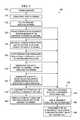
- FIG. 1presents a flow diagram illustrating selective steps in an example embodiment of a method of manufacturing an through-substrate-via structure of the disclosure and example embodiment of a method of manufacturing an integrated circuit of the disclosure;
- the present disclosurebenefits from the observation that during the manufacture of an IC, using a process that includes forming a metal-filled TSV before other IC components are fabricated, can result in lower-than-desired IC device yields or reliability.
- a problem which can be encounteredis cracking caused by the mismatch of the expansion of the metal in the TSV and the surrounding substrate, occurring during subsequent heat treatments in the fabrication and interconnection of the IC components. For instance, cracking in the substrate may lead to failure of the IC when exposed to the high temperature processing required for metal layer and dielectric layer fabrication to interconnect the IC components.
- TSV fabrication performed after IC component fabricationcan also result in lower-than-desired device yields.
- TSV fabricationcan include filling TSV opening in the back-side of the substrate with a metal after the device components have been fabricated on the front-side of the substrate.
- this processrequires that the back-side TSV opening be well-aligned with the metal interconnects formed on the front-side of the substrate.
- Embodiments of the present disclosureaddress these deficiencies by providing an improved method of manufacturing TSV and IC.
- the methoduses front-side processing which includes forming a front-side TSV opening which is front-side filled with a fill material.
- the front-side processingis followed by back-side processing which includes removing portions of the fill material and back-side filling of the TSV with an electrically conductive material.
- This processcan help ensure that the TSV is aligned with the metal interconnects formed on the front-side of the substrate while at the same time avoid cracking of the substrate during the front-side fabrication of IC components that can include high temperature processes (e.g., temperature of about 200° C. or higher).
- FIG. 1presents a flow diagram illustrating selective steps in an example embodiment of a method 100 of manufacture of an example through-substrate via.
- the method 100comprises a step 105 of providing a substrate having a front-side and an opposite back-side.
- the method 100also comprises a step 110 of forming through-substrate via opening in the front-side of the substrate.
- the method 100further includes a step 115 of filling the through-substrate via opening with a solid fill material.
- the method 100additionally comprises a step 120 of removing portions of the substrate from the outer surface of the back-side of the substrate to thereby expose the fill material.
- the method 100also comprises a step 125 of removing at least portions of the exposed fill material to form a back-side through-substrate via opening that traverses an entire thickness of the substrate.
- the methodfurther comprises a step 130 of filling the back-side through-substrate via opening with an electrically conductive material.
- FIG. 1also illustrates another embodiment of the disclosure, a method 102 of manufacturing an integrated circuit.
- the method 102comprises the step 105 of providing a substrate and method 100 of forming through-substrate via structure including steps 110 - 130 .
- FIGS. 2-12present cross-sectional views of selected steps in an example method of manufacturing an example TSV structure 200 of the disclosure, in accordance with the example method presented in FIG. 1 .
- the TSV structure 200is included in an example IC 202 of the disclosure.
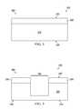
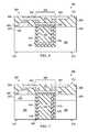
- FIG. 2shows the TSV structure 200 and IC 202 after the step 105 of providing a substrate 205 having a front-side 210 and an opposite back-side 215 .
- Example embodiments of the substrate 205include a wafer substrate composed of silicon or other semiconductor materials, substrate dies, package substrates, or interposer substrates. Some embodiments of the substrate 205 can have multiple layers to facilitate the efficient fabrication of various IC components.
- the substrate 205include a constituent layer 220 .
- the constituent layer 220can include a mono-crystalline layer composed of silicon such as epitaxial-formed crystalline silicon.
- the constituent layer 220can include a silicon-on-insulator layer, or polysilicon layer or other material layers well known to those skilled in the art.
- the constituent layer 220can have a thickness 222 in a range from 10 to 20 microns.
- substrates and constituent layerscould be used, if desired.
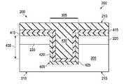
- FIG. 3shows the TSV structure 200 and IC 202 after the step 110 of forming a through-substrate via opening 305 in the front-side 210 of the substrate 205 .
- One of ordinary skill in the artwould be familiar with the procedures to pattern (e.g., by conventional photolithography and masking processes) and to etch (e.g., reactive ion etching or other conventional etching processes) the front-side 210 of the substrate 205 to form the opening 305 in accordance with step 110 .
- the through-substrate-via opening 305is formed so as to not penetrate an outer surface 310 of the back-side 215 of the substrate 205 .
- FIG. 4shows the TSV structure 200 and IC 202 after the step 115 of filling the TSV opening 305 with a solid fill material 405 .
- CVDchemical vapor deposition
- PVDphysical vapor deposition
- the fill material 405has a coefficient of thermal expansion that is within about 10 percent, and more preferably within about 1 percent, of a coefficient of thermal expansion of the substrate 205 .
- the step 115 of filling the TSV opening 305 with the fill material 405includes filling the opening 305 with one or more insulating materials, e.g., that includes a passivation layer 410 , and a diffusion barrier layer 415 .
- one or both of these layers 410 , 415can coat the interior walls (e.g., sidewalls 420 and floor 425 ) of the TSV opening 305 .
- the filling step 115can include filling the opening 305 with an insulating material 405 that includes an insulating plug 430 .
- the insulating plug 430includes or is a dielectric material such as silica glass, and more preferably in some cases, borophosphosilicate glass.
- the step 115 of filling the TSV opening 305 with the fill material 405includes filling material 405 that includes multiple layers of insulating material: a passivation layer 410 of silicon oxide that coats the interior walls 420 and floor 425 the opening 305 ; a diffusion barrier layer 415 of silicon nitride on the passivation layer 410 (e.g., coating the passivation layer 410 ) and an insulating plug 430 of a dielectric material (e.g., silica glass) contacting the diffusion barrier layer 415 and substantially filling the entire depth or remaining entire depth 435 (e.g., the volume of the opening 305 not occupied by other insulating layers 410 , 415 when present) of the front-side through-substrate via opening 305 .
- a passivation layer 410 of silicon oxidethat coats the interior walls 420 and floor 425 the opening 305
- a diffusion barrier layer 415 of silicon nitride on the passivation layer 410e.g.
- some embodiments of the methods 100 , 102further include a step 135 of removing the fill material 405 from an exterior surface 505 of the front-side 210 of the substrate 205 that lay outside of the front-side opening 305 .
- One of ordinary skill in the artwould be familiar techniques such as chemical mechanical polishing (CMP) to perform step 135 so as to polish and planarize the front-side exterior surface 505 down to the level of the substrate 205 (or its constituent layer 220 ).
- CMPchemical mechanical polishing
- some embodiments of the methods 100 , 102also include a step 140 of covering the front-side through-substrate via opening 305 with an electrically conductive layer 610 .
- Forming the electrically conductive layer 610helps to mark the location of the TSV structure 200 and thereby helps ensure that the TSV structure 200 will be aligned with the subsequently formed metal interconnects on the front-side of the substrate.
- the back-side through-substrate via opening formed in step 125is done after step 140 to cover the front-side through-substrate via opening with the electrically conductive layer 610 . This order of steps has the advantage of avoiding the back-side opening from being filled with materials associated with the forming the front-side electrically conductive layer covering 610 .
- a second insulating layer 620(including, e.g., a barrier layer such as a silicon nitride layer) is formed on the front-side surface 505 (e.g., via conventional PVD or CVD processes). Then the electrically conductive layer 610 of a metal (e.g., a copper layer or other metal such as tungsten or gold) is formed on the second insulating layer 620 , (e.g., in some cases by sputter depositing a metal seed layer such tungsten, gold or copper) and then electro-chemically forming another metal layer on the seed layer. The electrically conductive layer 610 and second insulating layer 620 can then be patterned using conventional processes to remove these layers 610 , 620 from the surface 505 except for those portions that cover the opening 305 .
- a metale.g., a copper layer or other metal such as tungsten or gold
- some embodiments of the method 102 of manufacturing the IC 202also includes a step 145 of forming active or passive electrical components 630 on the front-side 210 of the substrate 205 .
- active components 630such as resistors or inductors, or active components, such as memory circuit components (e.g., SRAM or DRAM memory) or logic circuit components (e.g., CMOS or bi-CMOS logic integrated circuits).
- the back-side through-substrate via opening formed in step 125is done after step 145 of forming the active or passive electrical components 630 . This order of steps has the advantage of avoiding the back-side opening from being filled with materials associated with the forming the components 630 .
- some embodiments of the method 102 of manufacturing the IC 202further include a step 150 of forming interconnect structures 640 (e.g., copper or other metal lines, vias, and landing pads) on the front-side 210 of the substrate 205 .
- interconnect structures 640e.g., copper or other metal lines, vias, and landing pads
- One of ordinary skill in the artwould be familiar with the procedures to form the interconnect structures 640 .
- one or more interlayer dielectric layers 650can be formed on the front-side 210 to support and electrically insulate the interconnect structures 640 and the passive or active components 630 .
- At least one of the interconnect structures 640contacts (directly or indirectly through additional interconnect structures 640 ) the electrically conductive layer 610 covering a front-side TSV opening 305 , and, also contacts an active or passive component 630 on the substrate 205 . That is, the interconnect structure 640 electrically interconnects the active or passive component 630 to the TSV through the electrically conductive layer 610 . In other embodiments, however, the TSV or its electrically conductive cover layer 610 may not be coupled to any active or passive component 630 or interconnect structure 640 on the substrate 205 , and instead, may simply pass through the substrate 205 .
- step 145it is preferable to form the active or passive components 630 in step 145 before filling the TSV opening 305 with an electrically conductive material (step 130 ) that has a higher thermal expansion coefficient than the substrate (e.g., a metal such as copper).
- step 130an electrically conductive material that has a higher thermal expansion coefficient than the substrate (e.g., a metal such as copper).
- the interconnect structures 630 in step 150it is preferable to form the interconnect structures 630 in step 150 before step 130 .
- this ordering of stepscan help avoid thermal expansion stresses and strains on the substrate 205 during high-temperature fabrication processes that may be used as part of steps 145 or 150 .
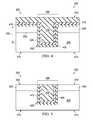
- FIG. 7shows the TSV structure 200 and IC 202 after the step 120 of removing portions of the substrate 205 from the outer surface 310 of the back-side 215 of the substrate 205 to thereby expose the fill material 405 .
- CMPcan be used to polish and planarize the back-side surface 310 until the fill material 405 in the TSV opening 305 is exposed.
- other types of removal procedurese.g., wet and dry etching
- FIG. 8shows the TSV structure 200 and IC 202 after the step 125 of removing at least portions of the exposed fill material 405 to form a back-side through-substrate via opening 810 .
- the back-side through-substrate via opening 810traverses an entire thickness 820 of the substrate 205 .
- retaining a passivation layer 410 and barrier layer 415 on the sidewalls 420 of the TSV opening 305can be advantageous when the back-side through-substrate via opening 810 is to be filled in step 130 with an electrically conductive material composed of highly diffusible metal atoms (e.g., copper atoms). Diffusible metal atoms can detrimentally diffuse from the TSV 200 into the substrate 205 , including those regions of the substrate 205 where the active and passive components 630 are located, thereby damaging such components 630 .
- highly diffusible metal atomse.g., copper atoms
- the removing step 125can include a wet etch process (e.g., a hydrofluoric acid etch process).
- a wet etch processe.g., a hydrofluoric acid etch process
- One skilled in the artwould be familiar with how to configure the wet etch process so as to leave the passivation layer 410 and barrier layer 415 substantially intact on the sidewalls 420 .
- a dry etch processmay be used performed to selectively remove the insulating plug 430 that traverses the thickness 820 of substrate 205 .
- some embodiments of the methods 100 , 102further include a step 155 of removing an insulating material (e.g., portions of the second insulating layer 620 , FIG. 6 ) located on an electrically conductive layer 610 and that covers the front-side 210 of the through-substrate via opening 305 .
- the removing step 155can include a plasma etch process directed through the back-side through-substrate via opening 810 to remove portions of the second insulating layer 620 over the opening 810 so as to expose an interior surface 910 of the electrically conductive material 610 covering the opening 810 .
- step 115facilitates electrical coupling of the electrically conductive layer 610 to the electrically conductive material that the opening 810 is subsequently filled with in step 130 .
- step 115further includes removing the insulating material 620 on the electrically conductive layer 610 covering the front-side of the through-substrate via opening 810 by a plasma etch process directed through the back-side through-substrate via opening 810 .
- plasma etch processdirected through the back-side through-substrate via opening 810 .
- Non-limiting examples of the types of electrically conductive material 1010 that could be usedincludes copper, tungsten, gold, polysilicon, or similar materials familiar to those skilled in the art.
- the filling step 130can be advantageous for the filling step 130 to include forming (e.g., sputter depositing) a metal seed layer 1020 (e.g., a copper seed layer) on the interior side walls 1030 and floor (e.g., the interior surface 910 ) of the back-side opening 810 .
- the interior sidewalls 1030can include one or more intervening insulating layers 410 , 415 that were front-side formed in step 115 .
- the filling step 130can further include electrochemically forming a bulk metal 1040 (e.g., on the metal seed layer 1020 to fill the back-side through-substrate via opening 810 .
- the electrically conductive material 1010forms a solid (i.e., a void-free) conductive plug that entirely fills the opening 810 .
- some embodiments of the methods 100 , 102further include a step 160 of removing the electrically conductive material 1010 from the back-side surface 310 of the substrate 205 that lies outside of the back-side through-substrate via opening 810 .
- a step 160 of removing the electrically conductive material 1010 from the back-side surface 310 of the substrate 205 that lies outside of the back-side through-substrate via opening 810One of ordinary skill in the art would be familiar with techniques such as CMP to perform step 160 so as to polish and planarize the back-side surface 310 down to the level of the substrate 205 , such that the substrate outer surface 310 on the back-side 215 is exposed.
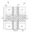
- some embodiments of the method 102 of manufacturing the IC 202further include a step 165 of interconnecting the TSV structure 200 of the substrate 205 to another TSV structure 1210 of another substrate 1220 that is vertically stacked with the substrate 205 .
- a step 165 of interconnecting the TSV structure 200 of the substrate 205 to another TSV structure 1210 of another substrate 1220 that is vertically stacked with the substrate 205One of ordinary skill in the art would be familiar with procedures, such as flip chip bonding processes, to facilitate stacking of the substrates 205 , 1220 such that the TSVs 200 , 1210 are interconnected.
- the substrates 200 , 1210 and IC 202can be part of an IC package 1225 .
- embodiments of the IC 202could further include shallow trench isolation structures located between the passive or active components 630 or between TSV structures 200 and the passive or active components 630 .
- FIGS. 1-12illustrate still another embodiment of the disclosure, a through-substrate-via structure 200 .
- Embodiments of the through-substrate-via structure 200can be manufactured by a method 100 that includes steps 110 - 130 as discussed in the context of FIG. 1 .
- Embodiments of the method 100 of forming the through-substrate-via structure 200can include embodiments of steps 110 - 130 as further discussed in the context of FIGS. 1-12 and could include any of the features discussed above in the context of FIGS. 1-12 .
- FIGS. 1-12illustrate yet another embodiment of the disclosure, an integrated circuit.
- the example IC 202comprises a substrate 205 and a through-substrate-via structure 200 that traverses the substrate 205 .
- the through-substrate-via structure 200is formed by a method 100 that includes steps 110 - 130 shown in FIG. 1 .
- Embodiments of the IC 205can include any of the features discussed above in the context of FIGS. 1-12 .
Landscapes
- Engineering & Computer Science (AREA)
- Power Engineering (AREA)
- Microelectronics & Electronic Packaging (AREA)
- Physics & Mathematics (AREA)
- Condensed Matter Physics & Semiconductors (AREA)
- General Physics & Mathematics (AREA)
- Computer Hardware Design (AREA)
- Manufacturing & Machinery (AREA)
- Internal Circuitry In Semiconductor Integrated Circuit Devices (AREA)
Abstract
Description
- The present application is related to U.S. patent application Ser. No. ______ (docket no. L10-0269US1) to M. A. Bachman, S. M. Merchant and J. Osenbach, entitled, INTEGRATION OF SHALLOW TRENCH ISOLATION AND THROUGH-SUBSTRATE VIAS INTO INTEGRATED CIRCUIT DESIGNS (“Bachman et al.”), and which is commonly assigned with the present application, which is incorporated herein by reference in its entirety.
- This application is directed, in general, to integrated circuit fabrication and, more specifically, to through-substrate via fabrication.
- Through-Substrate Via (TSV) technology is being developed in the large scale integrated circuit package industry to facilitate the fabrication and design of a three-dimensional interconnect system. Using TSVs, connections can be made from an integrated circuit (IC) on the front-side (the side on which the IC components are fabricated) of a substrate die through the same die to the dies' back-side, where a connection can be made to another substrate die, interconnect structure, interposer, or IC package substrate. The efficient fabrication of such TSVs, which may number in the hundreds or thousands per die, is an important aspect of IC package cost, performance and reliability.
- The present disclosure provides, in one embodiment, a method of manufacturing a through-substrate-via structure. The method comprises providing a substrate having a front-side and an opposite back-side. A through-substrate via opening is formed in the front-side of the substrate. The through-substrate-via opening does not penetrate an outer surface of the back-side of the substrate. The through-substrate-via opening is filled with a solid fill material. Portions of the substrate from the outer surface of the back-side of the substrate are removed to thereby expose the fill material. At least portions of the exposed fill material are removed to form a back-side through-substrate via opening that traverses an entire thickness of the substrate. The back-side through-substrate via opening is filled with an electrically conductive material.
- Another embodiment is a method of manufacturing an integrated circuit that comprises providing a substrate having a front-side and an opposite back-side and forming a through-substrate-via structure by the above-described steps.
- Still another embodiment is a through-substrate-via structure manufactured by a method that includes the above-described steps.
- Yet another embodiment is an integrated circuit, comprising a substrate and a through-substrate-via structure via that traverses the substrate, wherein the through-substrate-via structure is formed by the above-described steps.
- For a more complete understanding of the present invention, reference is now made to the following descriptions taken in conjunction with the accompanying drawings, in which:
FIG. 1 presents a flow diagram illustrating selective steps in an example embodiment of a method of manufacturing an through-substrate-via structure of the disclosure and example embodiment of a method of manufacturing an integrated circuit of the disclosure; andFIGS. 2-12 present cross-sectional views of selected steps in an example method of manufacturing an example through-substrate-via structure and an example integrated circuit of the disclosure in accordance with the method presented inFIG. 1 .- For the purposes of the present disclosure, the term, “or,” as used herein, refers to a non-exclusive or, unless otherwise indicated.
- The present disclosure benefits from the observation that during the manufacture of an IC, using a process that includes forming a metal-filled TSV before other IC components are fabricated, can result in lower-than-desired IC device yields or reliability. A problem which can be encountered is cracking caused by the mismatch of the expansion of the metal in the TSV and the surrounding substrate, occurring during subsequent heat treatments in the fabrication and interconnection of the IC components. For instance, cracking in the substrate may lead to failure of the IC when exposed to the high temperature processing required for metal layer and dielectric layer fabrication to interconnect the IC components.
- In other cases, TSV fabrication performed after IC component fabrication can also result in lower-than-desired device yields. For instance, TSV fabrication can include filling TSV opening in the back-side of the substrate with a metal after the device components have been fabricated on the front-side of the substrate. However, this process requires that the back-side TSV opening be well-aligned with the metal interconnects formed on the front-side of the substrate.
- Embodiments of the present disclosure address these deficiencies by providing an improved method of manufacturing TSV and IC. The method uses front-side processing which includes forming a front-side TSV opening which is front-side filled with a fill material. The front-side processing is followed by back-side processing which includes removing portions of the fill material and back-side filling of the TSV with an electrically conductive material. This process can help ensure that the TSV is aligned with the metal interconnects formed on the front-side of the substrate while at the same time avoid cracking of the substrate during the front-side fabrication of IC components that can include high temperature processes (e.g., temperature of about 200° C. or higher).
- One embodiment of the disclosure is a method of manufacturing a through-substrate via.
FIG. 1 presents a flow diagram illustrating selective steps in an example embodiment of amethod 100 of manufacture of an example through-substrate via. - The
method 100 comprises astep 105 of providing a substrate having a front-side and an opposite back-side. Themethod 100 also comprises astep 110 of forming through-substrate via opening in the front-side of the substrate. Themethod 100 further includes astep 115 of filling the through-substrate via opening with a solid fill material. Themethod 100 additionally comprises astep 120 of removing portions of the substrate from the outer surface of the back-side of the substrate to thereby expose the fill material. Themethod 100 also comprises astep 125 of removing at least portions of the exposed fill material to form a back-side through-substrate via opening that traverses an entire thickness of the substrate. The method further comprises astep 130 of filling the back-side through-substrate via opening with an electrically conductive material. FIG. 1 also illustrates another embodiment of the disclosure, amethod 102 of manufacturing an integrated circuit. Themethod 102 comprises thestep 105 of providing a substrate andmethod 100 of forming through-substrate via structure including steps110-130.- To further illustrate aspects of the disclosed methods,100,102,
FIGS. 2-12 present cross-sectional views of selected steps in an example method of manufacturing anexample TSV structure 200 of the disclosure, in accordance with the example method presented inFIG. 1 . The TSVstructure 200 is included in anexample IC 202 of the disclosure. With continuing reference toFIG. 1 throughout,FIG. 2 shows the TSVstructure 200 and IC202 after thestep 105 of providing asubstrate 205 having a front-side 210 and an opposite back-side 215. Example embodiments of thesubstrate 205 include a wafer substrate composed of silicon or other semiconductor materials, substrate dies, package substrates, or interposer substrates. Some embodiments of thesubstrate 205 can have multiple layers to facilitate the efficient fabrication of various IC components. For instance, some embodiments of thesubstrate 205 include aconstituent layer 220. For example, some embodiments of theconstituent layer 220 can include a mono-crystalline layer composed of silicon such as epitaxial-formed crystalline silicon. In other embodiments, theconstituent layer 220 can include a silicon-on-insulator layer, or polysilicon layer or other material layers well known to those skilled in the art. In some cases, theconstituent layer 220 can have a thickness222 in a range from 10 to 20 microns. One of ordinary skill would appreciate that other types of substrates and constituent layers could be used, if desired. FIG. 3 shows the TSVstructure 200 and IC202 after thestep 110 of forming a through-substrate viaopening 305 in the front-side 210 of thesubstrate 205. One of ordinary skill in the art would be familiar with the procedures to pattern (e.g., by conventional photolithography and masking processes) and to etch (e.g., reactive ion etching or other conventional etching processes) the front-side 210 of thesubstrate 205 to form the opening305 in accordance withstep 110. As illustrated inFIG. 3 , the through-substrate-viaopening 305 is formed so as to not penetrate anouter surface 310 of the back-side 215 of thesubstrate 205.FIG. 4 shows the TSVstructure 200 and IC202 after thestep 115 of filling the TSV opening305 with asolid fill material 405. One of ordinary skill in the art would be familiar with conventional filling methods such as chemical vapor deposition (CVD), physical vapor deposition (PVD) or both, or other methods, to accomplish thefilling step 115.- Filling the
opening 305 with a material405 whose coefficient of thermal expansion is close to that of thesubstrate 205 helps to avoid producing stresses or strains on the substrate when thesubstrate 205 is heated, e.g., as part of various process steps in the fabrication of an IC or IC package. In some embodiments, for instance, thefill material 405 has a coefficient of thermal expansion that is within about 10 percent, and more preferably within about 1 percent, of a coefficient of thermal expansion of thesubstrate 205. - In some cases, the
step 115 of filling theTSV opening 305 with thefill material 405 includes filling theopening 305 with one or more insulating materials, e.g., that includes apassivation layer 410, and adiffusion barrier layer 415. One or both of theselayers TSV opening 305. - As further illustrated in
FIG. 4 , in some cases the fillingstep 115 can include filling theopening 305 with an insulatingmaterial 405 that includes an insulatingplug 430. In some cases the insulatingplug 430 includes or is a dielectric material such as silica glass, and more preferably in some cases, borophosphosilicate glass. - In some cases, the
step 115 of filling theTSV opening 305 with thefill material 405 includes fillingmaterial 405 that includes multiple layers of insulating material: apassivation layer 410 of silicon oxide that coats theinterior walls 420 andfloor 425 theopening 305; adiffusion barrier layer 415 of silicon nitride on the passivation layer410 (e.g., coating the passivation layer410) and an insulatingplug 430 of a dielectric material (e.g., silica glass) contacting thediffusion barrier layer 415 and substantially filling the entire depth or remaining entire depth435 (e.g., the volume of theopening 305 not occupied by other insulatinglayers opening 305. - As shown in
FIGS. 1 and 5 , some embodiments of themethods step 135 of removing thefill material 405 from anexterior surface 505 of the front-side 210 of thesubstrate 205 that lay outside of the front-side opening 305. One of ordinary skill in the art would be familiar techniques such as chemical mechanical polishing (CMP) to performstep 135 so as to polish and planarize the front-side exterior surface 505 down to the level of the substrate205 (or its constituent layer220). - As shown in
FIGS. 1 and 6 , some embodiments of themethods step 140 of covering the front-side through-substrate via opening305 with an electricallyconductive layer 610. Forming the electricallyconductive layer 610 helps to mark the location of theTSV structure 200 and thereby helps ensure that theTSV structure 200 will be aligned with the subsequently formed metal interconnects on the front-side of the substrate. In some embodiments, the back-side through-substrate via opening formed instep 125 is done afterstep 140 to cover the front-side through-substrate via opening with the electricallyconductive layer 610. This order of steps has the advantage of avoiding the back-side opening from being filled with materials associated with the forming the front-side electrically conductive layer covering610. - In some embodiments, as part of
step 140, a second insulating layer620 (including, e.g., a barrier layer such as a silicon nitride layer) is formed on the front-side surface505 (e.g., via conventional PVD or CVD processes). Then the electricallyconductive layer 610 of a metal (e.g., a copper layer or other metal such as tungsten or gold) is formed on the second insulatinglayer 620, (e.g., in some cases by sputter depositing a metal seed layer such tungsten, gold or copper) and then electro-chemically forming another metal layer on the seed layer. The electricallyconductive layer 610 and second insulatinglayer 620 can then be patterned using conventional processes to remove theselayers surface 505 except for those portions that cover theopening 305. - As also shown in
FIGS. 1 and 6 , some embodiments of themethod 102 of manufacturing theIC 202 also includes astep 145 of forming active or passiveelectrical components 630 on the front-side 210 of thesubstrate 205. One of ordinary skill in the art would be familiar with the procedures to fabricatepassive components 630, such as resistors or inductors, or active components, such as memory circuit components (e.g., SRAM or DRAM memory) or logic circuit components (e.g., CMOS or bi-CMOS logic integrated circuits). In some embodiments, the back-side through-substrate via opening formed instep 125 is done afterstep 145 of forming the active or passiveelectrical components 630. This order of steps has the advantage of avoiding the back-side opening from being filled with materials associated with the forming thecomponents 630. - As further shown in
FIGS. 1 and 6 , some embodiments of themethod 102 of manufacturing theIC 202 further include astep 150 of forming interconnect structures640 (e.g., copper or other metal lines, vias, and landing pads) on the front-side 210 of thesubstrate 205. One of ordinary skill in the art would be familiar with the procedures to form theinterconnect structures 640. For instance, as part ofstep 150, one or more interlayerdielectric layers 650 can be formed on the front-side 210 to support and electrically insulate theinterconnect structures 640 and the passive oractive components 630. - In some embodiments, at least one of the
interconnect structures 640 contacts (directly or indirectly through additional interconnect structures640) the electricallyconductive layer 610 covering a front-side TSV opening 305, and, also contacts an active orpassive component 630 on thesubstrate 205. That is, theinterconnect structure 640 electrically interconnects the active orpassive component 630 to the TSV through the electricallyconductive layer 610. In other embodiments, however, the TSV or its electricallyconductive cover layer 610 may not be coupled to any active orpassive component 630 orinterconnect structure 640 on thesubstrate 205, and instead, may simply pass through thesubstrate 205. - In some embodiments, it is preferable to form the active or
passive components 630 instep 145 before filling theTSV opening 305 with an electrically conductive material (step130) that has a higher thermal expansion coefficient than the substrate (e.g., a metal such as copper). Similarly, in some cases, it is preferable to form theinterconnect structures 630 instep 150 beforestep 130. For instance, this ordering of steps can help avoid thermal expansion stresses and strains on thesubstrate 205 during high-temperature fabrication processes that may be used as part ofsteps FIG. 7 shows theTSV structure 200 andIC 202 after thestep 120 of removing portions of thesubstrate 205 from theouter surface 310 of the back-side 215 of thesubstrate 205 to thereby expose thefill material 405. One of ordinary skill in the art would be familiar with procedures to achievestep 120. In some cases, for instance, CMP can be used to polish and planarize the back-side surface 310 until thefill material 405 in theTSV opening 305 is exposed. One skilled in the art would appreciate, however, that other types of removal procedures (e.g., wet and dry etching) could also be used to performstep 120.FIG. 8 shows theTSV structure 200 andIC 202 after thestep 125 of removing at least portions of the exposedfill material 405 to form a back-side through-substrate viaopening 810. In the illustrative embodiment, the back-side through-substrate viaopening 810 traverses anentire thickness 820 of thesubstrate 205.- In some cases, it is desirable to retain some of the insulating
material 405 inside of the back-side through-substrate viaopening 810. For instance, retaining apassivation layer 410 andbarrier layer 415 on thesidewalls 420 of theTSV opening 305 can be advantageous when the back-side through-substrate viaopening 810 is to be filled instep 130 with an electrically conductive material composed of highly diffusible metal atoms (e.g., copper atoms). Diffusible metal atoms can detrimentally diffuse from theTSV 200 into thesubstrate 205, including those regions of thesubstrate 205 where the active andpassive components 630 are located, thereby damagingsuch components 630. - In some cases, for example, the removing
step 125 can include a wet etch process (e.g., a hydrofluoric acid etch process). One skilled in the art would be familiar with how to configure the wet etch process so as to leave thepassivation layer 410 andbarrier layer 415 substantially intact on thesidewalls 420. For instance, when theplug 430 is composed of a silica glass material such as borophosphosilicate glass, a dry etch process may be used performed to selectively remove the insulatingplug 430 that traverses thethickness 820 ofsubstrate 205. In some cases, additionally or alternatively, a hydrofluoric acid wet etch through the back-side through-substrate viaopening 810 can be performed to selectively remove the insulatingplug 430 traversing thesubstrate 205, such that after such a wet-etch, thepassivation layer 410 of silicon oxide anddiffusion barrier layer 415 of silicon nitride are retained. - As shown in
FIGS. 1 and 9 , some embodiments of themethods step 155 of removing an insulating material (e.g., portions of the second insulatinglayer 620,FIG. 6 ) located on an electricallyconductive layer 610 and that covers the front-side 210 of the through-substrate viaopening 305. For instance, the removingstep 155 can include a plasma etch process directed through the back-side through-substrate viaopening 810 to remove portions of the second insulatinglayer 620 over theopening 810 so as to expose aninterior surface 910 of the electricallyconductive material 610 covering theopening 810. The removingstep 155 facilitates electrical coupling of the electricallyconductive layer 610 to the electrically conductive material that theopening 810 is subsequently filled with instep 130. For instance, in some cases step115 further includes removing the insulatingmaterial 620 on the electricallyconductive layer 610 covering the front-side of the through-substrate viaopening 810 by a plasma etch process directed through the back-side through-substrate viaopening 810. One skilled in the art would be familiar with how to configure the plasma etch processes so as to leave thepassivation layer 410 andbarrier layer 415 substantially intact on thesidewalls 420, if desired. FIG. 10 shows theTSV structure 200 andIC 202 after thestep 130 of filling the back-side through-substrate via opening810 with an electricallyconductive material 1010.- Non-limiting examples of the types of electrically
conductive material 1010 that could be used includes copper, tungsten, gold, polysilicon, or similar materials familiar to those skilled in the art. In some embodiments, to fill a deep back-side opening810 (e.g., where thesubstrate thickness 820,FIG. 8 , is about 50 microns or greater) it can be advantageous for the fillingstep 130 to include forming (e.g., sputter depositing) a metal seed layer1020 (e.g., a copper seed layer) on theinterior side walls 1030 and floor (e.g., the interior surface910) of the back-side opening 810. In some cases, theinterior sidewalls 1030 can include one or moreintervening insulating layers step 115. In some cases, the fillingstep 130 can further include electrochemically forming a bulk metal1040 (e.g., on themetal seed layer 1020 to fill the back-side through-substrate viaopening 810. In some preferred embodiments, the electricallyconductive material 1010 forms a solid (i.e., a void-free) conductive plug that entirely fills theopening 810. - As shown in
FIGS. 1 and 11 , some embodiments of themethods step 160 of removing the electricallyconductive material 1010 from the back-side surface 310 of thesubstrate 205 that lies outside of the back-side through-substrate viaopening 810. One of ordinary skill in the art would be familiar with techniques such as CMP to performstep 160 so as to polish and planarize the back-side surface 310 down to the level of thesubstrate 205, such that the substrateouter surface 310 on the back-side 215 is exposed. - As shown in
FIGS. 1 and 12 , some embodiments of themethod 102 of manufacturing theIC 202 further include astep 165 of interconnecting theTSV structure 200 of thesubstrate 205 to anotherTSV structure 1210 of anothersubstrate 1220 that is vertically stacked with thesubstrate 205. One of ordinary skill in the art would be familiar with procedures, such as flip chip bonding processes, to facilitate stacking of thesubstrates TSVs substrates IC 202 can be part of anIC package 1225. - As illustrated in
FIG. 12 , in some embodiments, the front-side 210 of thesubstrate 205 faces the front-side 1230 of theother substrate 1220. In other embodiments, however, the back-side 210 of thesubstrate 205 can face the back-side 1240 of theother substrate 1220. In still other embodiments, there could be astack 1250 ofmultiple substrates TSVs - Additionally, as further explained in Bachman et al., embodiments of the
IC 202 could further include shallow trench isolation structures located between the passive oractive components 630 or betweenTSV structures 200 and the passive oractive components 630. FIGS. 1-12 illustrate still another embodiment of the disclosure, a through-substrate-viastructure 200. Embodiments of the through-substrate-viastructure 200 can be manufactured by amethod 100 that includes steps110-130 as discussed in the context ofFIG. 1 . Embodiments of themethod 100 of forming the through-substrate-viastructure 200 can include embodiments of steps110-130 as further discussed in the context ofFIGS. 1-12 and could include any of the features discussed above in the context ofFIGS. 1-12 .FIGS. 1-12 illustrate yet another embodiment of the disclosure, an integrated circuit. With continuing reference toFIGS. 1-12 . Theexample IC 202 comprises asubstrate 205 and a through-substrate-viastructure 200 that traverses thesubstrate 205. The through-substrate-viastructure 200 is formed by amethod 100 that includes steps110-130 shown inFIG. 1 . Embodiments of theIC 205 can include any of the features discussed above in the context ofFIGS. 1-12 .- Those skilled in the art to which this application relates will appreciate that other and further additions, deletions, substitutions and modifications may be made to the described embodiments.
Claims (20)
Priority Applications (2)
| Application Number | Priority Date | Filing Date | Title |
|---|---|---|---|
| US12/969,836US8987137B2 (en) | 2010-12-16 | 2010-12-16 | Method of fabrication of through-substrate vias |
| US14/251,258US9613847B2 (en) | 2010-12-16 | 2014-04-11 | Integration of shallow trench isolation and through-substrate vias into integrated circuit designs |
Applications Claiming Priority (1)
| Application Number | Priority Date | Filing Date | Title |
|---|---|---|---|
| US12/969,836US8987137B2 (en) | 2010-12-16 | 2010-12-16 | Method of fabrication of through-substrate vias |
Publications (2)
| Publication Number | Publication Date |
|---|---|
| US20120153492A1true US20120153492A1 (en) | 2012-06-21 |
| US8987137B2 US8987137B2 (en) | 2015-03-24 |
Family
ID=46233333
Family Applications (1)
| Application Number | Title | Priority Date | Filing Date |
|---|---|---|---|
| US12/969,836Active2033-10-05US8987137B2 (en) | 2010-12-16 | 2010-12-16 | Method of fabrication of through-substrate vias |
Country Status (1)
| Country | Link |
|---|---|
| US (1) | US8987137B2 (en) |
Cited By (17)
| Publication number | Priority date | Publication date | Assignee | Title |
|---|---|---|---|---|
| US20110014582A1 (en)* | 2009-07-16 | 2011-01-20 | Memc Singapore Pte. Ltd. (Uen200614794D) | Coated crucibles and methods for applying a coating to a crucible |
| US20120235261A1 (en)* | 2011-03-17 | 2012-09-20 | Seiko Epson Corporation | Device-mounted substrate, infrared light sensor and through electrode forming method |
| US20130119543A1 (en)* | 2011-11-16 | 2013-05-16 | Globalfoundries Singapore Pte. Ltd. | Through silicon via for stacked wafer connections |
| US20130147036A1 (en)* | 2011-12-13 | 2013-06-13 | Stats Chippac, Ltd. | Semiconductor Device and Method of Forming UBM Structure on Back Surface of TSV Semiconductor Wafer |
| US20140057434A1 (en)* | 2012-08-24 | 2014-02-27 | Jia-Jia Chen | Through silicon via process |
| US20140264911A1 (en)* | 2013-03-15 | 2014-09-18 | Globalfoundries Singapore Pte. Ltd. | Through silicon vias |
| US8987137B2 (en) | 2010-12-16 | 2015-03-24 | Lsi Corporation | Method of fabrication of through-substrate vias |
| US9613847B2 (en) | 2010-12-16 | 2017-04-04 | Avago Technologies General Ip (Singapore) Pte. Ltd. | Integration of shallow trench isolation and through-substrate vias into integrated circuit designs |
| FR3059464A1 (en)* | 2016-11-29 | 2018-06-01 | Commissariat A L'energie Atomique Et Aux Energies Alternatives | ELECTRONIC CIRCUIT COMPRISING TRENCHES OF ELECTRICAL INSULATION |
| CN111403395A (en)* | 2020-03-30 | 2020-07-10 | 长江存储科技有限责任公司 | Three-dimensional memory and manufacturing method thereof |
| US20200365447A1 (en)* | 2017-09-28 | 2020-11-19 | Intel Corporation | Filling openings by combining non-flowable and flowable processes |
| US10861792B2 (en)* | 2019-03-25 | 2020-12-08 | Raytheon Company | Patterned wafer solder diffusion barrier |
| US20210343332A1 (en)* | 2020-04-30 | 2021-11-04 | Taiwan Semiconductor Manufacturing Co., Ltd. | Sram Structure with Asymmetric Interconnection |
| CN114566461A (en)* | 2022-03-02 | 2022-05-31 | 成都海威华芯科技有限公司 | Semiconductor device deep back hole manufacturing method and device based on front and back side through holes |
| WO2022147430A1 (en)* | 2020-12-28 | 2022-07-07 | Invensas Bonding Technologies, Inc. | Structures with through-substrate vias and methods for forming the same |
| US11594452B2 (en)* | 2015-09-24 | 2023-02-28 | Intel Corporation | Techniques for revealing a backside of an integrated circuit device, and associated configurations |
| US11756880B2 (en) | 2018-10-22 | 2023-09-12 | Adeia Semiconductor Bonding Technologies Inc. | Interconnect structures |
Families Citing this family (12)
| Publication number | Priority date | Publication date | Assignee | Title |
|---|---|---|---|---|
| US11069734B2 (en) | 2014-12-11 | 2021-07-20 | Invensas Corporation | Image sensor device |
| US10204893B2 (en) | 2016-05-19 | 2019-02-12 | Invensas Bonding Technologies, Inc. | Stacked dies and methods for forming bonded structures |
| US10290495B2 (en)* | 2016-07-29 | 2019-05-14 | Japan Display Inc. | Electronic apparatus and manufacturing method of the same |
| US11097942B2 (en) | 2016-10-26 | 2021-08-24 | Analog Devices, Inc. | Through silicon via (TSV) formation in integrated circuits |
| US10217720B2 (en) | 2017-06-15 | 2019-02-26 | Invensas Corporation | Multi-chip modules formed using wafer-level processing of a reconstitute wafer |
| US11276676B2 (en) | 2018-05-15 | 2022-03-15 | Invensas Bonding Technologies, Inc. | Stacked devices and methods of fabrication |
| US11462419B2 (en) | 2018-07-06 | 2022-10-04 | Invensas Bonding Technologies, Inc. | Microelectronic assemblies |
| US11158606B2 (en) | 2018-07-06 | 2021-10-26 | Invensas Bonding Technologies, Inc. | Molded direct bonded and interconnected stack |
| US11296053B2 (en) | 2019-06-26 | 2022-04-05 | Invensas Bonding Technologies, Inc. | Direct bonded stack structures for increased reliability and improved yield in microelectronics |
| US11631647B2 (en) | 2020-06-30 | 2023-04-18 | Adeia Semiconductor Bonding Technologies Inc. | Integrated device packages with integrated device die and dummy element |
| US11728273B2 (en) | 2020-09-04 | 2023-08-15 | Adeia Semiconductor Bonding Technologies Inc. | Bonded structure with interconnect structure |
| US11764177B2 (en) | 2020-09-04 | 2023-09-19 | Adeia Semiconductor Bonding Technologies Inc. | Bonded structure with interconnect structure |
Citations (3)
| Publication number | Priority date | Publication date | Assignee | Title |
|---|---|---|---|---|
| US20110033980A1 (en)* | 2007-06-26 | 2011-02-10 | Hynix Semiconductor Inc. | Stack package that prevents warping and cracking of a wafer and semiconductor chip and method for manufacturing the same |
| US20130119543A1 (en)* | 2011-11-16 | 2013-05-16 | Globalfoundries Singapore Pte. Ltd. | Through silicon via for stacked wafer connections |
| US20130299950A1 (en)* | 2012-05-11 | 2013-11-14 | Sematech, Inc. | Semiconductor structure with buried through substrate vias |
Family Cites Families (14)
| Publication number | Priority date | Publication date | Assignee | Title |
|---|---|---|---|---|
| US7276787B2 (en) | 2003-12-05 | 2007-10-02 | International Business Machines Corporation | Silicon chip carrier with conductive through-vias and method for fabricating same |
| JP4389227B2 (en) | 2006-09-28 | 2009-12-24 | エルピーダメモリ株式会社 | Manufacturing method of semiconductor device |
| US7879711B2 (en) | 2006-11-28 | 2011-02-01 | Taiwan Semiconductor Manufacturing Co., Ltd. | Stacked structures and methods of fabricating stacked structures |
| US7645678B2 (en) | 2007-02-13 | 2010-01-12 | United Microelectronics Corp. | Process of manufacturing a shallow trench isolation and process of treating bottom surface of the shallow trench for avoiding bubble defects |
| KR100895813B1 (en) | 2007-06-20 | 2009-05-06 | 주식회사 하이닉스반도체 | Manufacturing method of semiconductor package |
| US7939941B2 (en) | 2007-06-27 | 2011-05-10 | Taiwan Semiconductor Manufacturing Company, Ltd. | Formation of through via before contact processing |
| JP5361156B2 (en) | 2007-08-06 | 2013-12-04 | ラピスセミコンダクタ株式会社 | Semiconductor device and manufacturing method thereof |
| US7859114B2 (en) | 2008-07-29 | 2010-12-28 | International Business Machines Corporation | IC chip and design structure with through wafer vias dishing correction |
| KR20100040455A (en) | 2008-10-10 | 2010-04-20 | 주식회사 동부하이텍 | Method for fabricating of semiconductor device |
| US8097953B2 (en) | 2008-10-28 | 2012-01-17 | Taiwan Semiconductor Manufacturing Company, Ltd. | Three-dimensional integrated circuit stacking-joint interface structure |
| US20100224965A1 (en) | 2009-03-09 | 2010-09-09 | Chien-Li Kuo | Through-silicon via structure and method for making the same |
| US8492241B2 (en) | 2010-10-14 | 2013-07-23 | International Business Machines Corporation | Method for simultaneously forming a through silicon via and a deep trench structure |
| US8987137B2 (en) | 2010-12-16 | 2015-03-24 | Lsi Corporation | Method of fabrication of through-substrate vias |
| US8742535B2 (en) | 2010-12-16 | 2014-06-03 | Lsi Corporation | Integration of shallow trench isolation and through-substrate vias into integrated circuit designs |
- 2010
- 2010-12-16USUS12/969,836patent/US8987137B2/enactiveActive
Patent Citations (3)
| Publication number | Priority date | Publication date | Assignee | Title |
|---|---|---|---|---|
| US20110033980A1 (en)* | 2007-06-26 | 2011-02-10 | Hynix Semiconductor Inc. | Stack package that prevents warping and cracking of a wafer and semiconductor chip and method for manufacturing the same |
| US20130119543A1 (en)* | 2011-11-16 | 2013-05-16 | Globalfoundries Singapore Pte. Ltd. | Through silicon via for stacked wafer connections |
| US20130299950A1 (en)* | 2012-05-11 | 2013-11-14 | Sematech, Inc. | Semiconductor structure with buried through substrate vias |
Cited By (33)
| Publication number | Priority date | Publication date | Assignee | Title |
|---|---|---|---|---|
| US20110014582A1 (en)* | 2009-07-16 | 2011-01-20 | Memc Singapore Pte. Ltd. (Uen200614794D) | Coated crucibles and methods for applying a coating to a crucible |
| US9458551B2 (en)* | 2009-07-16 | 2016-10-04 | Memc Singapore Pte. Ltd. | Coated crucibles and methods for applying a coating to a crucible |
| US8987137B2 (en) | 2010-12-16 | 2015-03-24 | Lsi Corporation | Method of fabrication of through-substrate vias |
| US9613847B2 (en) | 2010-12-16 | 2017-04-04 | Avago Technologies General Ip (Singapore) Pte. Ltd. | Integration of shallow trench isolation and through-substrate vias into integrated circuit designs |
| US20120235261A1 (en)* | 2011-03-17 | 2012-09-20 | Seiko Epson Corporation | Device-mounted substrate, infrared light sensor and through electrode forming method |
| US9070637B2 (en)* | 2011-03-17 | 2015-06-30 | Seiko Epson Corporation | Device-mounted substrate, infrared light sensor and through electrode forming method |
| US20130119543A1 (en)* | 2011-11-16 | 2013-05-16 | Globalfoundries Singapore Pte. Ltd. | Through silicon via for stacked wafer connections |
| US8809191B2 (en)* | 2011-12-13 | 2014-08-19 | Stats Chippac, Ltd. | Semiconductor device and method of forming UBM structure on back surface of TSV semiconductor wafer |
| US9601462B2 (en)* | 2011-12-13 | 2017-03-21 | STATS ChipPAC Pte. Ltd. | Semiconductor device and method of forming UBM structure on back surface of TSV semiconductor wafer |
| US20140264851A1 (en)* | 2011-12-13 | 2014-09-18 | Stats Chippac, Ltd. | Semiconductor Device and Method of Forming UBM Structure on Back Surface of TSV Semiconductor Wafer |
| US20130147036A1 (en)* | 2011-12-13 | 2013-06-13 | Stats Chippac, Ltd. | Semiconductor Device and Method of Forming UBM Structure on Back Surface of TSV Semiconductor Wafer |
| US9012324B2 (en)* | 2012-08-24 | 2015-04-21 | United Microelectronics Corp. | Through silicon via process |
| US20140057434A1 (en)* | 2012-08-24 | 2014-02-27 | Jia-Jia Chen | Through silicon via process |
| US9287197B2 (en)* | 2013-03-15 | 2016-03-15 | Globalfoundries Singapore Pte. Ltd. | Through silicon vias |
| US20140264911A1 (en)* | 2013-03-15 | 2014-09-18 | Globalfoundries Singapore Pte. Ltd. | Through silicon vias |
| US11594452B2 (en)* | 2015-09-24 | 2023-02-28 | Intel Corporation | Techniques for revealing a backside of an integrated circuit device, and associated configurations |
| WO2018100273A1 (en)* | 2016-11-29 | 2018-06-07 | Commissariat A L'energie Atomique Et Aux Energies Alternatives | Electronic circuit comprising electrical insulation trenches |
| EP3549161B1 (en)* | 2016-11-29 | 2023-09-27 | Commissariat à l'énergie atomique et aux énergies alternatives | Electronic circuit comprising electrical insulation trenches |
| US11049762B2 (en) | 2016-11-29 | 2021-06-29 | Commissariat à l'énergie atomique et aux énergies alternatives | Electronic circuit comprising electrical insulation trenches |
| FR3059464A1 (en)* | 2016-11-29 | 2018-06-01 | Commissariat A L'energie Atomique Et Aux Energies Alternatives | ELECTRONIC CIRCUIT COMPRISING TRENCHES OF ELECTRICAL INSULATION |
| US20200365447A1 (en)* | 2017-09-28 | 2020-11-19 | Intel Corporation | Filling openings by combining non-flowable and flowable processes |
| US12300533B2 (en) | 2017-09-28 | 2025-05-13 | Intel Corporation | Filling openings by combining non-flowable and flowable processes |
| US11978657B2 (en)* | 2017-09-28 | 2024-05-07 | Intel Corporation | Filling openings by combining non-flowable and flowable processes |
| US12125784B2 (en) | 2018-10-22 | 2024-10-22 | Adeia Semiconductor Bonding Technologies Inc. | Interconnect structures |
| US11756880B2 (en) | 2018-10-22 | 2023-09-12 | Adeia Semiconductor Bonding Technologies Inc. | Interconnect structures |
| US10861792B2 (en)* | 2019-03-25 | 2020-12-08 | Raytheon Company | Patterned wafer solder diffusion barrier |
| CN111403395A (en)* | 2020-03-30 | 2020-07-10 | 长江存储科技有限责任公司 | Three-dimensional memory and manufacturing method thereof |
| US20210343332A1 (en)* | 2020-04-30 | 2021-11-04 | Taiwan Semiconductor Manufacturing Co., Ltd. | Sram Structure with Asymmetric Interconnection |
| US11521676B2 (en)* | 2020-04-30 | 2022-12-06 | Taiwan Semiconductor Manufacturing Company, Ltd. | SRAM structure with asymmetric interconnection |
| US11996140B2 (en) | 2020-04-30 | 2024-05-28 | Taiwan Semiconductor Manufacturing Company, Ltd. | SRAM structure with asymmetric interconnection |
| WO2022147430A1 (en)* | 2020-12-28 | 2022-07-07 | Invensas Bonding Technologies, Inc. | Structures with through-substrate vias and methods for forming the same |
| US12381128B2 (en) | 2020-12-28 | 2025-08-05 | Adeia Semiconductor Bonding Technologies Inc. | Structures with through-substrate vias and methods for forming the same |
| CN114566461A (en)* | 2022-03-02 | 2022-05-31 | 成都海威华芯科技有限公司 | Semiconductor device deep back hole manufacturing method and device based on front and back side through holes |
Also Published As
| Publication number | Publication date |
|---|---|
| US8987137B2 (en) | 2015-03-24 |
Similar Documents
| Publication | Publication Date | Title |
|---|---|---|
| US8987137B2 (en) | Method of fabrication of through-substrate vias | |
| US8742535B2 (en) | Integration of shallow trench isolation and through-substrate vias into integrated circuit designs | |
| US8501587B2 (en) | Stacked integrated chips and methods of fabrication thereof | |
| US8283207B2 (en) | Methods for forming through-substrate conductor filled vias, and electronic assemblies formed using such methods | |
| US8421193B2 (en) | Integrated circuit device having through via and method for preparing the same | |
| US8525343B2 (en) | Device with through-silicon via (TSV) and method of forming the same | |
| TWI525776B (en) | Optimized ring-shaped copper through-substrate perforation | |
| TWI441308B (en) | Stacked wafer for 3d integration | |
| US9984926B2 (en) | Solution for TSV substrate leakage | |
| TW201230279A (en) | Integrated circuit device and method of forming the same | |
| CN102237300B (en) | Through-substrate via structure and manufacturing method thereof | |
| US11508619B2 (en) | Electrical connection structure and method of forming the same | |
| CN102208363A (en) | Method for forming through silicon via | |
| US8587131B1 (en) | Through-silicon via and fabrication method thereof | |
| WO2013023456A1 (en) | Method for simultaneously preparing vertical conduction hold and first layer of re-wiring layer | |
| US9257337B2 (en) | Semiconductor structure and manufacturing method thereof | |
| WO2012048973A1 (en) | Methods of forming through wafer interconnects in semiconductor structures using sacrificial material, and semiconductor structures formed by such methods | |
| US20150179580A1 (en) | Hybrid interconnect structure and method for fabricating the same | |
| TW201101424A (en) | Method for fabricating through-silicon via structure | |
| TW201250970A (en) | Method for fabricating through-silicon via structure |
Legal Events
| Date | Code | Title | Description |
|---|---|---|---|
| AS | Assignment | Owner name:LSI CORPORATION, CALIFORNIA Free format text:ASSIGNMENT OF ASSIGNORS INTEREST;ASSIGNORS:BACHMAN, MARK A.;MERCHANT, SAILESH M.;OSENBACH, JOHN;SIGNING DATES FROM 20101215 TO 20110110;REEL/FRAME:025607/0198 | |
| AS | Assignment | Owner name:DEUTSCHE BANK AG NEW YORK BRANCH, AS COLLATERAL AG Free format text:PATENT SECURITY AGREEMENT;ASSIGNORS:LSI CORPORATION;AGERE SYSTEMS LLC;REEL/FRAME:032856/0031 Effective date:20140506 | |
| STCF | Information on status: patent grant | Free format text:PATENTED CASE | |
| AS | Assignment | Owner name:AVAGO TECHNOLOGIES GENERAL IP (SINGAPORE) PTE. LTD Free format text:ASSIGNMENT OF ASSIGNORS INTEREST;ASSIGNOR:LSI CORPORATION;REEL/FRAME:035390/0388 Effective date:20140814 | |
| AS | Assignment | Owner name:AGERE SYSTEMS LLC, PENNSYLVANIA Free format text:TERMINATION AND RELEASE OF SECURITY INTEREST IN PATENT RIGHTS (RELEASES RF 032856-0031);ASSIGNOR:DEUTSCHE BANK AG NEW YORK BRANCH, AS COLLATERAL AGENT;REEL/FRAME:037684/0039 Effective date:20160201 Owner name:LSI CORPORATION, CALIFORNIA Free format text:TERMINATION AND RELEASE OF SECURITY INTEREST IN PATENT RIGHTS (RELEASES RF 032856-0031);ASSIGNOR:DEUTSCHE BANK AG NEW YORK BRANCH, AS COLLATERAL AGENT;REEL/FRAME:037684/0039 Effective date:20160201 | |
| AS | Assignment | Owner name:BANK OF AMERICA, N.A., AS COLLATERAL AGENT, NORTH CAROLINA Free format text:PATENT SECURITY AGREEMENT;ASSIGNOR:AVAGO TECHNOLOGIES GENERAL IP (SINGAPORE) PTE. LTD.;REEL/FRAME:037808/0001 Effective date:20160201 Owner name:BANK OF AMERICA, N.A., AS COLLATERAL AGENT, NORTH Free format text:PATENT SECURITY AGREEMENT;ASSIGNOR:AVAGO TECHNOLOGIES GENERAL IP (SINGAPORE) PTE. LTD.;REEL/FRAME:037808/0001 Effective date:20160201 | |
| AS | Assignment | Owner name:AVAGO TECHNOLOGIES GENERAL IP (SINGAPORE) PTE. LTD., SINGAPORE Free format text:TERMINATION AND RELEASE OF SECURITY INTEREST IN PATENTS;ASSIGNOR:BANK OF AMERICA, N.A., AS COLLATERAL AGENT;REEL/FRAME:041710/0001 Effective date:20170119 Owner name:AVAGO TECHNOLOGIES GENERAL IP (SINGAPORE) PTE. LTD Free format text:TERMINATION AND RELEASE OF SECURITY INTEREST IN PATENTS;ASSIGNOR:BANK OF AMERICA, N.A., AS COLLATERAL AGENT;REEL/FRAME:041710/0001 Effective date:20170119 | |
| AS | Assignment | Owner name:BELL SEMICONDUCTOR, LLC, ILLINOIS Free format text:ASSIGNMENT OF ASSIGNORS INTEREST;ASSIGNORS:AVAGO TECHNOLOGIES GENERAL IP (SINGAPORE) PTE. LTD.;BROADCOM CORPORATION;REEL/FRAME:044886/0766 Effective date:20171208 | |
| AS | Assignment | Owner name:CORTLAND CAPITAL MARKET SERVICES LLC, AS COLLATERA Free format text:SECURITY INTEREST;ASSIGNORS:HILCO PATENT ACQUISITION 56, LLC;BELL SEMICONDUCTOR, LLC;BELL NORTHERN RESEARCH, LLC;REEL/FRAME:045216/0020 Effective date:20180124 | |
| MAFP | Maintenance fee payment | Free format text:PAYMENT OF MAINTENANCE FEE, 4TH YEAR, LARGE ENTITY (ORIGINAL EVENT CODE: M1551); ENTITY STATUS OF PATENT OWNER: LARGE ENTITY Year of fee payment:4 | |
| AS | Assignment | Owner name:BELL NORTHERN RESEARCH, LLC, ILLINOIS Free format text:RELEASE BY SECURED PARTY;ASSIGNOR:CORTLAND CAPITAL MARKET SERVICES LLC;REEL/FRAME:059723/0382 Effective date:20220401 Owner name:BELL SEMICONDUCTOR, LLC, ILLINOIS Free format text:RELEASE BY SECURED PARTY;ASSIGNOR:CORTLAND CAPITAL MARKET SERVICES LLC;REEL/FRAME:059723/0382 Effective date:20220401 Owner name:HILCO PATENT ACQUISITION 56, LLC, ILLINOIS Free format text:RELEASE BY SECURED PARTY;ASSIGNOR:CORTLAND CAPITAL MARKET SERVICES LLC;REEL/FRAME:059723/0382 Effective date:20220401 | |
| MAFP | Maintenance fee payment | Free format text:PAYMENT OF MAINTENANCE FEE, 8TH YEAR, LARGE ENTITY (ORIGINAL EVENT CODE: M1552); ENTITY STATUS OF PATENT OWNER: LARGE ENTITY Year of fee payment:8 |