US20120126883A1 - Vertically stacked fin transistors and methods of fabricating and operating the same - Google Patents
Vertically stacked fin transistors and methods of fabricating and operating the sameDownload PDFInfo
- Publication number
- US20120126883A1 US20120126883A1US12/950,761US95076110AUS2012126883A1US 20120126883 A1US20120126883 A1US 20120126883A1US 95076110 AUS95076110 AUS 95076110AUS 2012126883 A1US2012126883 A1US 2012126883A1
- Authority
- US
- United States
- Prior art keywords
- gate
- trench
- transistor
- transistors
- fin
- Prior art date
- Legal status (The legal status is an assumption and is not a legal conclusion. Google has not performed a legal analysis and makes no representation as to the accuracy of the status listed.)
- Granted
Links
Images


Classifications
- H—ELECTRICITY
- H10—SEMICONDUCTOR DEVICES; ELECTRIC SOLID-STATE DEVICES NOT OTHERWISE PROVIDED FOR
- H10B—ELECTRONIC MEMORY DEVICES
- H10B12/00—Dynamic random access memory [DRAM] devices
- H10B12/01—Manufacture or treatment
- H10B12/02—Manufacture or treatment for one transistor one-capacitor [1T-1C] memory cells
- H10B12/05—Making the transistor
- H10B12/056—Making the transistor the transistor being a FinFET
- H—ELECTRICITY
- H10—SEMICONDUCTOR DEVICES; ELECTRIC SOLID-STATE DEVICES NOT OTHERWISE PROVIDED FOR
- H10B—ELECTRONIC MEMORY DEVICES
- H10B12/00—Dynamic random access memory [DRAM] devices
- H10B12/30—DRAM devices comprising one-transistor - one-capacitor [1T-1C] memory cells
- H10B12/36—DRAM devices comprising one-transistor - one-capacitor [1T-1C] memory cells the transistor being a FinFET
- H—ELECTRICITY
- H10—SEMICONDUCTOR DEVICES; ELECTRIC SOLID-STATE DEVICES NOT OTHERWISE PROVIDED FOR
- H10D—INORGANIC ELECTRIC SEMICONDUCTOR DEVICES
- H10D84/00—Integrated devices formed in or on semiconductor substrates that comprise only semiconducting layers, e.g. on Si wafers or on GaAs-on-Si wafers
- H10D84/01—Manufacture or treatment
- H10D84/0123—Integrating together multiple components covered by H10D12/00 or H10D30/00, e.g. integrating multiple IGBTs
- H10D84/0126—Integrating together multiple components covered by H10D12/00 or H10D30/00, e.g. integrating multiple IGBTs the components including insulated gates, e.g. IGFETs
- H10D84/0158—Integrating together multiple components covered by H10D12/00 or H10D30/00, e.g. integrating multiple IGBTs the components including insulated gates, e.g. IGFETs the components including FinFETs
- H—ELECTRICITY
- H10—SEMICONDUCTOR DEVICES; ELECTRIC SOLID-STATE DEVICES NOT OTHERWISE PROVIDED FOR
- H10D—INORGANIC ELECTRIC SEMICONDUCTOR DEVICES
- H10D84/00—Integrated devices formed in or on semiconductor substrates that comprise only semiconducting layers, e.g. on Si wafers or on GaAs-on-Si wafers
- H10D84/01—Manufacture or treatment
- H10D84/02—Manufacture or treatment characterised by using material-based technologies
- H10D84/03—Manufacture or treatment characterised by using material-based technologies using Group IV technology, e.g. silicon technology or silicon-carbide [SiC] technology
- H10D84/038—Manufacture or treatment characterised by using material-based technologies using Group IV technology, e.g. silicon technology or silicon-carbide [SiC] technology using silicon technology, e.g. SiGe
- H—ELECTRICITY
- H10—SEMICONDUCTOR DEVICES; ELECTRIC SOLID-STATE DEVICES NOT OTHERWISE PROVIDED FOR
- H10D—INORGANIC ELECTRIC SEMICONDUCTOR DEVICES
- H10D84/00—Integrated devices formed in or on semiconductor substrates that comprise only semiconducting layers, e.g. on Si wafers or on GaAs-on-Si wafers
- H10D84/80—Integrated devices formed in or on semiconductor substrates that comprise only semiconducting layers, e.g. on Si wafers or on GaAs-on-Si wafers characterised by the integration of at least one component covered by groups H10D12/00 or H10D30/00, e.g. integration of IGFETs
- H10D84/82—Integrated devices formed in or on semiconductor substrates that comprise only semiconducting layers, e.g. on Si wafers or on GaAs-on-Si wafers characterised by the integration of at least one component covered by groups H10D12/00 or H10D30/00, e.g. integration of IGFETs of only field-effect components
- H10D84/83—Integrated devices formed in or on semiconductor substrates that comprise only semiconducting layers, e.g. on Si wafers or on GaAs-on-Si wafers characterised by the integration of at least one component covered by groups H10D12/00 or H10D30/00, e.g. integration of IGFETs of only field-effect components of only insulated-gate FETs [IGFET]
- H10D84/834—Integrated devices formed in or on semiconductor substrates that comprise only semiconducting layers, e.g. on Si wafers or on GaAs-on-Si wafers characterised by the integration of at least one component covered by groups H10D12/00 or H10D30/00, e.g. integration of IGFETs of only field-effect components of only insulated-gate FETs [IGFET] comprising FinFETs
Definitions
- Embodiments of the inventionrelates generally to electronic devices, and more specifically, to non-planar transistors and techniques for fabricating the same.
- Fin field effect transistorsare often built around a fin (e.g., a tall, thin, semiconductive member) extending generally perpendicularly from a substrate.
- a gatetraverses the fin by conformally running up one side of the fin over the top and down the other side of the fin.
- a source and a drainare located on opposite sides of the gate in the fin. In operation, a current through the fin between the source and drain is controlled by selectively biasing the gate.
- High aspect ratio finstypically are desirable but challenging to construct.
- high aspect ratio finFETscan be integrated into a small area of the substrate, thereby potentially reducing manufacturing costs on a per-transistor basis.
- the width of each fin, and the gap between each finmay be reduced.
- construction of gates or other structures, and operation of the transistorsmay be increasingly difficult.
- FIGS. 1-8depict an embodiment of a process for forming deep isolation trenches of a semiconductor device in accordance with an embodiment of the present invention
- FIGS. 9-11depict an embodiment of a process for forming first shallow trenches in the device of FIG. 1 in accordance with an embodiment of the present invention
- FIGS. 12-14depict an embodiment of a process for forming second shallow trenches in the device of FIG. 1 in accordance with an embodiment of the present invention
- FIGS. 15 and 16depict an embodiment of a process for forming row trenches in the device of FIG. 1 in accordance with an embodiment of the present invention
- FIGS. 17 and 18depict an embodiment of a process for forming lower gates in the device of FIG. 1 in accordance with an embodiment of the present invention
- FIGS. 19-22depict an embodiment of a process for forming lower gates in the device of FIG. 1 in accordance with an embodiment of the present invention
- FIG. 23is a side view of a fin having transistors and gates formed using the techniques of FIGS. 1-22 ;
- FIG. 24is flowchart depicting the manufacturing process of FIGS. 1-22 in accordance with an embodiment of the present invention.
- FIGS. 25 and 26depict operation of an array portion having upper gates, lower gates, and vertically offset transistors in accordance with an embodiment of the present invention.
- Some of the subsequently discussed embodimentsmay facilitate the manufacture of high aspect ratio structures, such as finFETs having vertically offset transistors and stacked and interleaved access lines (e.g., wordlines).
- the vertically offset transistorsmay be formed at different depths between deep isolation trenches using multiple masking and etching process.
- upper and lower gatesmay be formed between each fin to form the access lines. The upper transistors may be activated by biasing the upper gates and the lower transistors may be activated by biasing the lower gates.
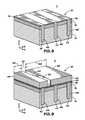
- FIG. 1depicts a cross-sectional plane view of a substrate 10 of a portion 11 of a semiconductor device for fabricating high aspect ratio structures, e.g., fins, of a memory array in accordance with an embodiment of the present invention.
- finrefers to a tall, thin, semiconductor member extending from a substrate and generally having a length (x-direction) greater than the width (y-direction) and greater than the depth (z-direction) of the fin.
- the substrate 10may include semiconductive materials such as single crystalline or poly crystalline silicon, gallium arsenide, indium phosphide, or other materials with semiconductor properties.
- the substrate 10may include a non-semiconductor surface on which an electronic device may be constructed such as a plastic or ceramic work surface, for example.
- the substrate 10may be in the form of a whole wafer, a portion of a diced wafer, or a portion of a diced wafer in a packaged electronic device, for instance.
- the substrate 10may include an upper doped region 12 and a lower doped region 14 .
- the depth of the upper doped region 12may be generally uniform over a substantial area of the substrate 10 , and the upper doped region 12 may be doped differently from the lower doped region 14 .
- the upper doped region 12may include an n+ material and the lower doped region 14 may include a p ⁇ material or vise versa.
- a pad oxide 16may be formed directly on the upper doped region 12 .
- the pad oxide 16may have a thickness less than 300 ⁇ , e.g., generally about 80 ⁇ .
- a stop body 18may be formed on the pad oxide 16 .
- the stop body 18may include a nitride and it may have a thickness less than about 300 ⁇ , e.g., generally about 95 ⁇ , but like the other structures described herein, the stop body 18 is not limited to these dimensions or materials.
- a sacrificial body 20may be formed on the stop body 18 .
- the sacrificial body 20may be made of polysilicon and it may have a thickness between about 500 ⁇ and about 2,000 ⁇ , e.g., generally about 1000 ⁇ .
- a lower masking body 22may be formed on the sacrificial body 20 .
- the lower masking body 22may be made of an oxide and it may have a thickness between about 500 ⁇ and about 2,000 ⁇ , e.g., generally about 1000 ⁇ .
- an upper masking body 24may be formed on the lower masking body 22 .
- the upper masking body 24may be made of carbon, and it may have a thickness between about 1000 ⁇ and about 3000 ⁇ , e.g., generally about 2000 ⁇ .
- These materials 16 , 18 , 20 , 22 and othersmay be formed with chemical-vapor deposition, spun-on coatings, or other processes know in the art.
- a column mask 26may be formed, as illustrated by FIG. 2 .
- the term “column”does not refer to any particular horizontal direction on the substrate 10 other than a direction that is different from the direction that subsequently-introduced rows extend.
- the column mask 26may include a pattern of lines that define masked regions having a width 28 and exposed regions having a width 30 .
- the widths 28 and 30may be generally equal to each other or generally different widths, and each generally equal to the lithographic-resolution limit (e.g., the photolithographic-resolution limit or minimum achievable feature size), referred to as “F.”
- the column mask 26may have a pitch 32 that is generally equal to F, 2 F, or other dimensions.
- the lines formed by the column mask 26may be generally straight, generally parallel to each other, and may generally extend in the y-direction. These lines may be generally continuous and generally uniform in the y-direction. In other embodiments, though, the lines formed by the column mask 26 may have other shapes, e.g., they may undulate (e.g., up and down, left and right, or both), they may vary in width in the y-direction, or they may be formed from a plurality of shorter segments.
- a column hard mask 34may be formed, as illustrated by FIG. 3 .
- the column hard mask 34may be formed by generally-anisotropically etching (e.g., with a directional plasma etch) the portion of the upper masking body 24 and the portion of the lower masking body 22 that are disposed under the region not covered by the column mask 26 .
- the etchmay stop on or in the sacrificial body 20 .
- the column spacers 36may be formed on the sidewalls of the column hard mask 34 , as illustrated by FIG. 4 .
- the column spacers 36may be formed by depositing a generally conformal film (e.g., a film that is of generally uniform thickness on both vertical and horizontal structures) and, then, anisotropically etching that film to remove it from horizontal surfaces, leaving material disposed against generally vertical surfaces on the substrate 10 .
- the column spacers 36may be made of an oxide, and they may have a width 38 that is less than about 100 nm.
- the column spacers 36may narrow the area exposed by the column hard mask 34 to a width 40 that is less than or equal to F, e.g., generally equal to or less than 3 ⁇ 4 F, 1 ⁇ 2 F, or 1 ⁇ 4 F.
- column isolation trenches 42may be formed.
- the column isolation trenches 42may be formed by generally anisotropically etching the exposed regions between the column spacers 36 .
- the column isolation trenches 42may have a width 41 that corresponds to (e.g., is generally equal to or proportional to) the width 40 .
- the column isolation trenches 42may generally extend in the y-direction and may be generally parallel to each other and generally straight.
- the cross-sectional shape of the column isolation trenches 42may be generally uniform in the y-direction.
- the column isolation trenches 42may have a depth 44 .
- the column isolation trenches 42may be patterned and etched using a conventional mask without the formation of sidewalls.
- the trenches 42may be formed through the sacrificial body 20 , the stop body 18 , the pad oxide 16 , the upper doped region 12 , and ending in the lower doped region 14 .
- the column isolation trenches 42may be filled partially or entirely with a dielectric 46 , as illustrated by FIG. 6 .
- the dielectric 46may be made of a variety of materials, such as an oxide, and it may be lined with a variety of liner films (not shown), such as an oxide liner and a nitride liner.
- the bottom of the column isolation trenches 42may be implanted or diffused with a dopant selected to further electrically isolate structures on opposing sides of the column isolation trenches 42 .
- Planarizing the substrate 10may include etching the substrate 10 or polishing the substrate with chemical-mechanical planarization or other methods. Planarization may include removing both the upper masking body 24 and the lower masking body 22 , and planarization may stop on or in the sacrificial body 20 . Additionally, an upper portion of the dielectric 46 maybe removed.
- the sacrificial body 20 and dielectric 46may be partially or entirely removed, as illustrated by FIG. 8 .
- Removing this body 20 and dielectric 46may include wet etching or dry etching the substrate 10 with an etch that selectively etches the sacrificial body 20 without removing a substantial portion of the exposed dielectric 46 , i.e., with an etch that is selective to the sacrificial body 20 .
- An etchis said to be “selective to” a material if the etch removes that material faster than other types of material.
- a first shallow trench mask 48is formed on the substrate 10 , as illustrated by FIG. 9 .
- another stop body 49may also be formed on the pad oxide 16 .
- the shallow trench mask 48may be photoresist or a hard mask, and it may be patterned with various lithographic systems, such as those discussed above.
- the illustrated shallow trench mask 48includes exposed regions 50 that may have a width 52 generally equal to or less than 1 ⁇ 4 F, 1 ⁇ 2 F or F, a first covered region 54 with a width 56 , and a second covered region 58 with a width 60 .
- the exposed regions 50may be generally linear, generally parallel, and interposed generally equidistant between every other one of the deep isolation trenches 42 .
- the exposed region 50 , the first covered region 54 , and the second covered region 58may be patterned on the substrate 10 in the x-direction forming exposed regions 50 between every other pair of deep isolation trenches 42 .
- the first shallow trench mask 48may be formed with spacers formed on sidewalls of the mask, similar to the techniques described above during formation of the column isolation trenches 42 .
- first shallow trenches 62may be formed to a depth 63 .
- the first shallow trenches 62may be generally linear, generally parallel, generally extend generally laterally in the y-direction and generally downward in the z-direction, and thus, may be generally parallel to the deep isolation trenches 42 .
- the shallow trenches 62are formed with a generally anisotropic dry etch and are deeper than the upper doped region 12 , but not as deep as the deep isolation trenches 42 .
- the shallow trenches 62may have a generally rectangular or generally trapezoidal profile that is generally uniform in the y-direction over a substantial distance. Additionally, before, during, or after the formation of the first shallow trenches 62 , the exposed regions 50 may be implanted with a dopant to form deep upper doped regions 64 . As explained further below, the deep upper doped regions 64 may form the source and drain regions of a deep transistor formed by the first shallow trenches 62 .
- the first shallow trenches 62are filled with a dielectric 66 , such as such as high density plasma (HDP) oxide, tetra-ethyl-ortho-silicate (TEOS), or spun-on-glass (SOG), and the substrate 10 is planarized to remove mask 48 .
- the shallow trenches 62may be filled with a different material than the deep isolation trenches 42 .
- the dielectric 66may be the same material used to fill the deep isolation trenches 42 .
- the dielectric 66 formed in the trenches 62provides for formation of a channel between a source and drain formed by the deep upper doped region 64 .
- a second shallow trench mask 68is formed on the substrate 10 .
- another stop body (e.g., a layer) 69may also be formed on the pad oxide 16 .
- the second shallow trench mask 68may be photoresist or a hard mask, and it may be patterned with various lithographic systems, such as those discussed above.
- the illustrated shallow trench mask 68includes exposed regions 70 that may have a width 72 generally equal to or less than 1 ⁇ 4 F, 1 ⁇ 2 F or F, a first covered region 74 with a width 76 , and a second covered region 78 with a width 80 .
- the exposed regions 70may be generally linear, generally parallel, and interposed generally equidistant between every other one of the deep isolation trenches 42 .
- the exposed region 70 , the first covered region 74 , and the second covered region 78may be patterned on the substrate 10 in the x-direction forming exposed regions 70 between every other pair of deep isolation trenches 42 .
- the second shallow trench mask 68may be formed with spacers formed on sidewalls of the mask, similar to the techniques described above during formation of the column isolation trenches 42 .
- the exposed regions 70 of the substrate 10may be etched to form second shallow trenches 82 , as illustrated by FIG. 13 .
- the second shallow trenches 82may be formed to a depth 83 , wherein the depth 83 is less than the depth 63 .
- the second shallow trenches 82may be generally linear, generally parallel, extend generally laterally in the y-direction and generally downward in the z-direction, and thus, may be generally parallel to the deep isolation trenches 42 .
- the second shallow trenches 82may be formed with a generally anisotropic dry etch and are deeper than the upper doped region 12 , but not as deep as the deep upper doped region 64 .
- the second shallow trenches 82may have a generally rectangular or generally trapezoidal profile that is generally uniform in the y-direction over a substantial distance.
- the second shallow trenches 82are filled with a dielectric 84 and the substrate 10 may be planarized to remove mask 68 .
- the second shallow trenches 82may be filled with a different material than the deep isolation trenches 42 and/or the first shallow trenches 62 .
- the dielectric 84may be the same material used to fill the deep isolation trenches 42 and/or the first shallow trenches 62 .
- the dielectric 84 formed in the trenches 82provides for formation of a channel between a source and drain formed by the upper doped region 12 on either side of the second shallow trenches 82 .
- a row mask 86may be formed, as illustrated by FIG. 15 .
- the row mask 86may be generally perpendicular to the column mask 26 ( FIG. 2 ). In other embodiments, the row mask 86 may be oriented differently with respect to the column mask 26 .
- the row mask 86may be formed with photoresist or it may be a hard mask, for example, and it may be patterned with photolithography or other lithographic processes, e.g., nano-imprint lithography or electron-beam lithography.
- the row mask 86may be formed by patterning a body of amorphous carbon that is formed on the substrate 10 .
- the amorphous carbonmay be formed with a thickness less than about 3000 ⁇ , e.g., a thickness less than or equal to about 2000 ⁇ .
- the row mask 86may define masked regions having a width 90 and exposed regions having a width 88 .
- the row mask 86may be formed with a sub-photolithographic process, e.g., a sidewall-spacer process, a resist-reflow process, or a line-width thinning process.
- the widths 88 or 90may be generally equal to or less than F, 3 ⁇ 4 F, or 1 ⁇ 2 F.
- the row mask 86may define a repeating pattern of lines with a pitch 92 , or in some embodiments, the pattern may be interrupted by other structures.
- the masked regions of the row mask 86may be generally straight, generally parallel to one another, and may generally extend in the x-direction. In other embodiments, the masked regions of the row mask 86 may undulate side to side or up and down, or they may be segmented.
- row trenches 94may be formed, as illustrated by FIG. 16 .
- the row trenches 94may define fins 96 disposed under the masked region of the row mask 86 .
- the row trenches 94may be formed with a dry etch that etches the upper doped region 12 , the lower doped region 14 , the dielectric 46 , and the dielectric 66 at generally the same rate.
- the row trenches 94may have a depth 98 that is greater than the depth of the first shallow trenches 62 ( FIG. 10 ) and less than a depth of the deep isolation trenches 42 ( FIG. 5 ).
- the fins 96may be generally defined by sidewalls 100 and bottom surfaces 102 of the trenches 94 .
- the width 90 of the fins 96may be about 30 nanometers, about 20 nanometers, or less, and the width 88 of the row trench 94 may be about 40 nanometers, about 30 nanometers, or less.
- each fin 96may include a lower transistor 104 formed by a source 106 and drain 108 of the deep upper doped region 64 and conductive channel 110 formed by the first shallow trenches 62 . Additionally, each also includes an upper transistor 112 formed by a source 114 and drain 116 of the upper doped region 12 and a conductive channel 118 formed by the second shallow trenches 82 . The upper transistor 112 is thus vertically offset from the lower transistor 104 relative to the bottom surfaces 102 . As explained further below, the lower transistors 104 of a fin 96 may be separately activated from the upper transistors 112 by biasing upper and lower gates, the formation of which is described below in FIGS. 17-22 .
- FIGS. 17 and 18depict formation of lower gates in the trenches 94 and adjacent to each of the sidewalls 100 .
- the term “lower”refers to the location of the gate relative to the trenches 94 , such that lower gates are nearer to the bottom surface of the trenches 94 .
- the lower gatesare relatively closer to the bottom surface 102 and farther from the upper portion of the fins 96 than subsequently formed upper gates.
- a gate oxide 118may be formed on the sidewalls 100 of the fins 96 and bottom portion 102 of the trenches 94 .
- the gate oxide 118may be deposited, grown, or otherwise formed, and it may substantially or entirely cover the exposed portions of the upper doped region 12 and the lower doped region 14 .
- the gate oxide 118may include a variety of dielectric materials, such as oxide (e.g., silicon dioxide), oxynitride, or high-dielectric constant materials like hafnium dioxide, zirconium dioxide, and titanium dioxide.
- the gate oxide 118may have a thickness less than about 60 ⁇ , e.g., a thickness equal to or less than about 40 ⁇ .
- a liner 120may be formed on the gate oxide 118 in accordance with an embodiment of the present invention. As shown in FIG. 17 , the liner 120 may be formed on the bottom surface 102 of the row trenches 96 and on the sidewalls 100 of the fins 96 .
- the liner 120may include titanium nitride (TiN), tungsten nitride, or other appropriate conductive materials or combination thereof.
- a metal conductor 122may be formed on the substrate 10 in accordance with an embodiment of the present invention.
- the metal conductor 122may fill the row trenches 94 and along the sidewalls 100 of the fins 96 .
- the metal conductor 122is deposited on top of the liner 120 . As will be appreciated, only that portion of the metal conductor 122 in the trenches 94 is illustrated.
- the metal conductor 122may include tungsten, ruthenium (Ru), or other appropriate conductive materials or combination thereof.
- titanium nitride liner 120may be disposed on the gate oxide 118 , and tungsten may be disposed on the titanium nitride liner 120 to form the metal conductor 122 .
- etching of the metal conductor 122may form bottom gates (e.g., wordlines) in the row trenches 94 on either the sidewalls 100 of the fins 96 .
- FIG. 18depicts the substrate 10 after a removal of a portion of the metal conductor 122 , the liner 120 , and the gate oxide 118 to form a lower gate 124 in accordance with an embodiment of the present invention.
- the liner 120 and gate oxide 118may be removed along the sidewalls 100 of the fins 96 to a depth 126 .
- the metal conductor 122may be removed to a depth 128 in the trenches 94 .
- the metal conductor 122 , the liner 120 , and the gate oxide 118may be removed by one of or a combination of etch processes, such as wet etch, dry etch, or other suitable processes.
- the duration of the etchmay control the depth (e.g., distance) of the etch into the row trenches 96 . Additionally, in some embodiments, differing etch rates of the different materials may result in different depths 126 and 128 . For example, as shown in FIG. 18 , after etching, the metal conductor 122 may protrude slightly above the gate oxide 118 and the liner 120 , such that the depth 126 is less than the depth 128 . In other embodiments, the depth 126 may be equal to or greater than the depth 128 .
- FIGS. 19-22depict the formation of upper gates (e.g., access lines such as wordlines) in the trenches 94 and above the lower gates 124 .
- upperrefers to the location of the gate relative to the trenches 94 , such that the “upper” gates are closer to the upper portion of the fins 96 and farther from the bottom surface 102 than the previously formed lower gates 124 .
- the upper gatesmay be formed in the portions of the trenches 94 that remain after formation of the lower gates.
- FIG. 19depicts formation of a gate oxide 130 one sidewalls 100 of the fins 96 and on the lower gates 124 , such as on the metal conductor 122 , the liner 120 , and the gate oxide 118 .
- the gate oxide 130may be deposited, grown, or otherwise formed, and it may substantially or entirely cover the exposed portions of the upper doped region 12 and some of the lower doped region 14 .
- the gate oxide 130may include a variety of dielectric materials, such as oxide (e.g., silicon dioxide), oxynitride, or high-dielectric constant materials like hafnium dioxide, zirconium dioxide, and titanium dioxide.
- the gate oxide 130may have a thickness less than about 60 ⁇ , e.g., a thickness equal to or less than about 40 ⁇ .
- a liner 132may be formed on the gate oxide 130 in accordance with an embodiment of the present invention. As shown in FIG. 20 , the liner 132 may be formed on the oxide 130 and on the lower gates 124 and the sidewalls 100 of the fins 96 .
- the liner 132may include titanium nitride (TiN), tungsten nitride, or other appropriate conductive materials or combination thereof.
- a metal conductor 134may be formed on the substrate 10 in accordance with an embodiment of the present invention.
- the metal conductor 134may be formed in the row trenches 94 and on the liner 132 . As will be appreciated, only that portion of the metal conductor 134 formed in the trenches 94 is illustrated.
- the metal conductor 134may include tungsten, ruthenium (Ru), or other appropriate conductive materials or combination thereof.
- titanium nitride liner 132may be disposed on the gate oxide 130 , and tungsten may be disposed on the titanium nitride liner 132 to form the metal conductor 134 .
- etching of the metal conductor 134may form upper gates (e.g., access lines such as wordlines) in the row trenches 94 on the sidewalls 100 of the fins 96 and above the lower gates 124 .
- FIG. 22depicts the substrate 10 after a removal of a portion of the metal conductor 134 , the liner 132 , and the gate oxide 130 to form upper gates 136 in accordance with an embodiment of the present invention.
- the liner 132 and gate oxide 130may be removed along the sidewalls 100 of the fins 96 to a depth 138 .
- the metal conductor 134may be removed to a depth 140 in the portion 96 .
- the metal conductor 134 , the liner 132 , and the gate oxide 130may be removed by one or a combination of etch processes, such as wet etch, dry etch, or other suitable processes.
- the duration of the etchmay control the depth (e.g., distance) of the etch into portion 96 .
- the depths 138 and 140may be substantially equal, as shown in FIG. 22 .
- differing etch rates of the different materialsmay result in different depths 138 and 140 .
- the metal conductor 134 and liner 132may from upper gates 136 for accessing the upper transistors 112 of the fins. As described further below, upper gates 136 and lower gates 124 may be used to activate transistors 112 and 104 respectively.
- each access linee.g., gates 136 and 124
- each access lineconnects (i.e., forms a cross-point or cross-hair) with an access device (e.g., the transistors 104 and 112 respectively of fins 96 ).
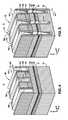
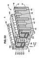
- FIG. 23is a side view of a fin 96 constructed in accordance with the techniques described above in FIGS. 1-22 .
- an upper gate 136 and a lower gate 124may be constructed on and extending parallel to a sidewall of the fin 96 in accordance with FIGS. 15-22 .
- the fin 96includes vertically offset transistors 104 and 112 constructed along the fin 96 in the x-direction.
- the lower transistors 104may include the source 106 and drain 108 formed in the deep upper doped region 64 and separated by the first shallow trenches 62 .
- biasing of the lower gate 124may activate the channel 110 of the transistors 104 and provide for operation of the lower transistors 104 .
- each of the upper transistorsinclude a source 114 and drain 116 formed in the upper doped region 12 and separated by the shallow trench 82 .
- the upper transistors 112are vertically offset from the lower transistors 104 and may be operated by the upper gate 136 to activate the channels 118 , as described below in FIG. 25 .
- FIG. 24is a flowchart summarizing a process 144 described above in FIGS. 1-22 .
- deep isolation trenchesmay be formed in the substrate 10 (block 146 ), as shown above in FIGS. 1-8 .
- the first shallow trench maskmay be patterned on the substrate 10 (block 148 ), as shown above in FIG. 9 .
- the open areas defined by the maskmay be implanted via a suitable dopant (block 150 ), and the open areas may be etched to form deep shallow trenches (block 152 ), as shown above in FIG. 10 .
- the implantationmay be performed before, during, or after the etch of the deep shallow trenches.
- a dielectricmay be deposited in the deep shallow trenches (block 154 ), as shown in FIG. 11 , and the substrate may be planarized in preparation for subsequent steps.
- the second shallow trench maskmay be formed on the substrate 10 (block 156 ), as shown in FIG. 12 , and the shallow trenches may be etched (block 158 ) as shown in FIG. 13 .
- a second dielectricmay be deposited in the shallow trenches (block 160 ) and the substrate 10 may be planarized.
- a row maskmay be patterned on the substrate (block 162 ), as shown in FIG. 15 , and row trenches may be etched into the substrate to form row trenches and fins (block 164 ), as shown in FIG. 16 .
- An oxidemay be formed in the row trenches on the sidewalls and bottom surface of the row trenches (block 166 ), as described in FIG. 17 .
- a linermay be formed on the oxide (block 168 ) and a metal conductor may be deposited in the row trenches (block 170 ), as also shown in FIG. 17 .
- the metal conductormay be etched to a desired depth to form the lower gates (block 172 ).
- another oxidemay be formed in the row trenches on the sidewalls of the fins and on the lower gates (block 174 ), as shown in FIG. 19 .
- a second linermay be formed on the second oxide (block 176 ), and a second metal conductor may be deposited in the row trenches and on the second liner (block 178 ), as shown in FIGS. 20 and 21 .
- the second metal conductormay be etched to a desired depth to form the upper gates (block 180 ).
- digitlines and storage devices accessible by the transistors of the fins 96may be formed on the array (block 182 ).
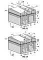
- FIGS. 25 and 26are schematic cross-sections of an array portion 190 formed in the manner described above in FIGS. 1-22 and depicting operation of upper gates 136 and lower gates 124 to operate the transistors of fins 96 .
- FIGS. 25 and 26depict fins 96 A- 96 F separated by row trenches 94 and each having upper gates 136 and lower gates 124 disposed therebetween and constructed according to the techniques described above.
- each fin 96 A, 96 C, and 96 Edepicts the lower transistors 104 and each of fins 96 B, 96 D, and 96 F depict the upper transistors 112 .
- the lower transistors 104 and the upper transistors 112may each be coupled to and used as access for devices for storage device disposed on the transistors 104 and 112 .
- upper transistors 112may be access devices for first storage devices and lower transistors 104 may be access devices for second storage devices.
- FIG. 25depicts operation of the upper transistors 112 of fins 96 B and 96 D in accordance with an embodiment of the present invention.
- the upper gate 192may be biased to a sufficient voltage to create current paths 118 and activate the upper transistors 112 .
- the lower gate 194is not actively biased to minimize or prevent current conduction to the lower gate 194 .
- the upper gate 196may be biased to a sufficient voltage to create current paths 118 and activate upper transistors 112 .
- the lower gate 198is not actively biased to minimize or prevent current conduction to the lower gate 198 .
- the upper transistors of fins 96 A, 96 C, and 96 Emay be activated by biasing the upper gates on the sidewalls of each respective fin.
- FIG. 26depicts operation of the lower transistors 104 of fins 96 C and 96 E in accordance with an embodiment of the present invention.
- a lower gate 200may be biased to a sufficient voltage to create current paths 110 and activate the lower transistors 112 .
- the upper gates 202are not actively biased to minimize or prevent undesirable current conduction.
- the lower gate 196may use the deep upper doped region 64 to bypass the inactive upper gates and conduct current to the lower gate 196 .
- a lower gate 204may be biased to a sufficient voltage to create current paths 110 along the fin 96 E and activate the lower transistors 112 .
- the upper gate 204 of fin 96 Eis not actively biased to minimize or avoid undesirable current conduction.
- the deep upper doped region 64 of fin 96 Eenables current to bypass the inactive upper gate 204 and conduct current to the lower gate 196 .
Landscapes
- Engineering & Computer Science (AREA)
- Manufacturing & Machinery (AREA)
- Insulated Gate Type Field-Effect Transistor (AREA)
- Semiconductor Memories (AREA)
- Metal-Oxide And Bipolar Metal-Oxide Semiconductor Integrated Circuits (AREA)
Abstract
Description
- 1. Field of Invention
- Embodiments of the invention relates generally to electronic devices, and more specifically, to non-planar transistors and techniques for fabricating the same.
- 2. Description of Related Art
- This section is intended to introduce the reader to various aspects of art that may be related to various aspects of the present invention, which are described and/or claimed below. This discussion is believed to be helpful in providing the reader with background information to facilitate a better understanding of the various aspects of the present invention. Accordingly, it should be understood that these statements are to be read in this light, and not as admissions of prior art.
- Fin field effect transistors (finFETs) are often built around a fin (e.g., a tall, thin, semiconductive member) extending generally perpendicularly from a substrate. Typically, a gate traverses the fin by conformally running up one side of the fin over the top and down the other side of the fin. Generally, a source and a drain are located on opposite sides of the gate in the fin. In operation, a current through the fin between the source and drain is controlled by selectively biasing the gate.
- High aspect ratio fins typically are desirable but challenging to construct. Generally, high aspect ratio finFETs can be integrated into a small area of the substrate, thereby potentially reducing manufacturing costs on a per-transistor basis. To increase density of the transistors, the width of each fin, and the gap between each fin, may be reduced. As the dimensions of the fin structures and the space between each fin are reduced, construction of gates or other structures, and operation of the transistors may be increasingly difficult.
FIGS. 1-8 depict an embodiment of a process for forming deep isolation trenches of a semiconductor device in accordance with an embodiment of the present invention;FIGS. 9-11 depict an embodiment of a process for forming first shallow trenches in the device ofFIG. 1 in accordance with an embodiment of the present invention;FIGS. 12-14 depict an embodiment of a process for forming second shallow trenches in the device ofFIG. 1 in accordance with an embodiment of the present invention;FIGS. 15 and 16 depict an embodiment of a process for forming row trenches in the device ofFIG. 1 in accordance with an embodiment of the present invention;FIGS. 17 and 18 depict an embodiment of a process for forming lower gates in the device ofFIG. 1 in accordance with an embodiment of the present invention;FIGS. 19-22 depict an embodiment of a process for forming lower gates in the device ofFIG. 1 in accordance with an embodiment of the present invention;FIG. 23 is a side view of a fin having transistors and gates formed using the techniques ofFIGS. 1-22 ;FIG. 24 is flowchart depicting the manufacturing process ofFIGS. 1-22 in accordance with an embodiment of the present invention; andFIGS. 25 and 26 depict operation of an array portion having upper gates, lower gates, and vertically offset transistors in accordance with an embodiment of the present invention.- Some of the subsequently discussed embodiments may facilitate the manufacture of high aspect ratio structures, such as finFETs having vertically offset transistors and stacked and interleaved access lines (e.g., wordlines). As is described in detail below, the vertically offset transistors may be formed at different depths between deep isolation trenches using multiple masking and etching process. Additionally, upper and lower gates may be formed between each fin to form the access lines. The upper transistors may be activated by biasing the upper gates and the lower transistors may be activated by biasing the lower gates. The following discussion describes devices and process flows in accordance with embodiments of the present technique.
FIG. 1 depicts a cross-sectional plane view of asubstrate 10 of aportion 11 of a semiconductor device for fabricating high aspect ratio structures, e.g., fins, of a memory array in accordance with an embodiment of the present invention. As used herein, the term “fin” refers to a tall, thin, semiconductor member extending from a substrate and generally having a length (x-direction) greater than the width (y-direction) and greater than the depth (z-direction) of the fin. Thesubstrate 10 may include semiconductive materials such as single crystalline or poly crystalline silicon, gallium arsenide, indium phosphide, or other materials with semiconductor properties. Alternatively, or additionally, thesubstrate 10 may include a non-semiconductor surface on which an electronic device may be constructed such as a plastic or ceramic work surface, for example. Thesubstrate 10 may be in the form of a whole wafer, a portion of a diced wafer, or a portion of a diced wafer in a packaged electronic device, for instance.- The
substrate 10 may include an upperdoped region 12 and a lowerdoped region 14. The depth of the upperdoped region 12 may be generally uniform over a substantial area of thesubstrate 10, and the upperdoped region 12 may be doped differently from the lowerdoped region 14. For example, the upperdoped region 12 may include an n+ material and the lowerdoped region 14 may include a p− material or vise versa. - Next, several materials may be formed on the
substrate 10, as illustrated byFIG. 1 . Apad oxide 16 may be formed directly on the upper dopedregion 12. Thepad oxide 16 may have a thickness less than 300 Å, e.g., generally about 80 Å. Astop body 18 may be formed on thepad oxide 16. Thestop body 18 may include a nitride and it may have a thickness less than about 300 Å, e.g., generally about 95 Å, but like the other structures described herein, thestop body 18 is not limited to these dimensions or materials. Asacrificial body 20 may be formed on thestop body 18. Thesacrificial body 20 may be made of polysilicon and it may have a thickness between about 500 Å and about 2,000 Å, e.g., generally about 1000 Å. Alower masking body 22 may be formed on thesacrificial body 20. Thelower masking body 22 may be made of an oxide and it may have a thickness between about 500 Å and about 2,000 Å, e.g., generally about 1000 Å. Finally, anupper masking body 24 may be formed on thelower masking body 22. Theupper masking body 24 may be made of carbon, and it may have a thickness between about 1000 Å and about 3000 Å, e.g., generally about 2000 Å. Thesematerials - Next, a
column mask 26 may be formed, as illustrated byFIG. 2 . (The term “column” does not refer to any particular horizontal direction on thesubstrate 10 other than a direction that is different from the direction that subsequently-introduced rows extend.) Thecolumn mask 26 may include a pattern of lines that define masked regions having awidth 28 and exposed regions having awidth 30. Thewidths column mask 26 may have apitch 32 that is generally equal to F, 2 F, or other dimensions. The lines formed by thecolumn mask 26 may be generally straight, generally parallel to each other, and may generally extend in the y-direction. These lines may be generally continuous and generally uniform in the y-direction. In other embodiments, though, the lines formed by thecolumn mask 26 may have other shapes, e.g., they may undulate (e.g., up and down, left and right, or both), they may vary in width in the y-direction, or they may be formed from a plurality of shorter segments. - After forming the
column mask 26, a columnhard mask 34 may be formed, as illustrated byFIG. 3 . The columnhard mask 34 may be formed by generally-anisotropically etching (e.g., with a directional plasma etch) the portion of theupper masking body 24 and the portion of thelower masking body 22 that are disposed under the region not covered by thecolumn mask 26. In some embodiments, the etch may stop on or in thesacrificial body 20. - Next, the
column mask 26 may be removed, and thecolumn spacers 36 may be formed on the sidewalls of the columnhard mask 34, as illustrated byFIG. 4 . Thecolumn spacers 36 may be formed by depositing a generally conformal film (e.g., a film that is of generally uniform thickness on both vertical and horizontal structures) and, then, anisotropically etching that film to remove it from horizontal surfaces, leaving material disposed against generally vertical surfaces on thesubstrate 10. The column spacers36 may be made of an oxide, and they may have awidth 38 that is less than about 100 nm. The column spacers36 may narrow the area exposed by the columnhard mask 34 to awidth 40 that is less than or equal to F, e.g., generally equal to or less than ¾ F, ½ F, or ¼ F. - Next, as illustrated by
FIG. 5 , column isolation trenches42 (also referred to as deep isolation trenches42) may be formed. Thecolumn isolation trenches 42 may be formed by generally anisotropically etching the exposed regions between thecolumn spacers 36. Thecolumn isolation trenches 42 may have awidth 41 that corresponds to (e.g., is generally equal to or proportional to) thewidth 40. Thecolumn isolation trenches 42 may generally extend in the y-direction and may be generally parallel to each other and generally straight. The cross-sectional shape of thecolumn isolation trenches 42 may be generally uniform in the y-direction. Thecolumn isolation trenches 42 may have adepth 44. Although the formation of thecolumn isolation trenches 42 described above inFIGS. 4 and 5 includes the formation of sidewalls, in other embodiments thecolumn isolation trenches 42 may be patterned and etched using a conventional mask without the formation of sidewalls. For example, in one embodiment, thetrenches 42 may be formed through thesacrificial body 20, thestop body 18, thepad oxide 16, the upper dopedregion 12, and ending in the lower dopedregion 14. - After forming the
column isolation trenches 42, they may be filled partially or entirely with a dielectric46, as illustrated byFIG. 6 . The dielectric46 may be made of a variety of materials, such as an oxide, and it may be lined with a variety of liner films (not shown), such as an oxide liner and a nitride liner. In some embodiments, prior to forming the dielectric46, the bottom of thecolumn isolation trenches 42 may be implanted or diffused with a dopant selected to further electrically isolate structures on opposing sides of thecolumn isolation trenches 42. - Next, the
substrate 10 may be planarized, as illustrated byFIG. 7 . Planarizing thesubstrate 10 may include etching thesubstrate 10 or polishing the substrate with chemical-mechanical planarization or other methods. Planarization may include removing both theupper masking body 24 and thelower masking body 22, and planarization may stop on or in thesacrificial body 20. Additionally, an upper portion of the dielectric46 maybe removed. - Next, the
sacrificial body 20 and dielectric46 may be partially or entirely removed, as illustrated byFIG. 8 . Removing thisbody 20 and dielectric46 may include wet etching or dry etching thesubstrate 10 with an etch that selectively etches thesacrificial body 20 without removing a substantial portion of the exposeddielectric 46, i.e., with an etch that is selective to thesacrificial body 20. An etch is said to be “selective to” a material if the etch removes that material faster than other types of material. - Next, a first
shallow trench mask 48 is formed on thesubstrate 10, as illustrated byFIG. 9 . In some embodiments, anotherstop body 49 may also be formed on thepad oxide 16. Theshallow trench mask 48 may be photoresist or a hard mask, and it may be patterned with various lithographic systems, such as those discussed above. The illustratedshallow trench mask 48 includes exposedregions 50 that may have awidth 52 generally equal to or less than ¼ F, ½ F or F, a firstcovered region 54 with awidth 56, and a secondcovered region 58 with awidth 60. The exposedregions 50 may be generally linear, generally parallel, and interposed generally equidistant between every other one of thedeep isolation trenches 42. Thus, the exposedregion 50, the firstcovered region 54, and the secondcovered region 58 may be patterned on thesubstrate 10 in the x-direction forming exposedregions 50 between every other pair ofdeep isolation trenches 42. In other embodiments, the firstshallow trench mask 48 may be formed with spacers formed on sidewalls of the mask, similar to the techniques described above during formation of thecolumn isolation trenches 42. - Next, the exposed
regions 50 of thesubstrate 10 may be etched, such as be dry etch or wet etch, to form firstshallow trenches 62, as illustrated byFIG. 10 . The firstshallow trenches 62 may be formed to adepth 63. The firstshallow trenches 62 may be generally linear, generally parallel, generally extend generally laterally in the y-direction and generally downward in the z-direction, and thus, may be generally parallel to thedeep isolation trenches 42. In this embodiment, theshallow trenches 62 are formed with a generally anisotropic dry etch and are deeper than the upper dopedregion 12, but not as deep as thedeep isolation trenches 42. Theshallow trenches 62 may have a generally rectangular or generally trapezoidal profile that is generally uniform in the y-direction over a substantial distance. Additionally, before, during, or after the formation of the firstshallow trenches 62, the exposedregions 50 may be implanted with a dopant to form deep upperdoped regions 64. As explained further below, the deep upperdoped regions 64 may form the source and drain regions of a deep transistor formed by the firstshallow trenches 62. - As illustrated in
FIG. 11 , the firstshallow trenches 62 are filled with a dielectric66, such as such as high density plasma (HDP) oxide, tetra-ethyl-ortho-silicate (TEOS), or spun-on-glass (SOG), and thesubstrate 10 is planarized to removemask 48. In some embodiments, theshallow trenches 62 may be filled with a different material than thedeep isolation trenches 42. In other embodiments, the dielectric66 may be the same material used to fill thedeep isolation trenches 42. As described below, the dielectric66 formed in thetrenches 62 provides for formation of a channel between a source and drain formed by the deep upperdoped region 64. - Next, as shown in
FIG. 12 , a secondshallow trench mask 68 is formed on thesubstrate 10. In some embodiments, another stop body (e.g., a layer)69 may also be formed on thepad oxide 16. The secondshallow trench mask 68 may be photoresist or a hard mask, and it may be patterned with various lithographic systems, such as those discussed above. The illustratedshallow trench mask 68 includes exposedregions 70 that may have awidth 72 generally equal to or less than ¼ F, ½ F or F, a firstcovered region 74 with awidth 76, and a secondcovered region 78 with awidth 80. The exposedregions 70 may be generally linear, generally parallel, and interposed generally equidistant between every other one of thedeep isolation trenches 42. Thus, the exposedregion 70, the firstcovered region 74, and the secondcovered region 78 may be patterned on thesubstrate 10 in the x-direction forming exposedregions 70 between every other pair ofdeep isolation trenches 42. In other embodiments, the secondshallow trench mask 68 may be formed with spacers formed on sidewalls of the mask, similar to the techniques described above during formation of thecolumn isolation trenches 42. - Next, the exposed
regions 70 of thesubstrate 10 may be etched to form secondshallow trenches 82, as illustrated byFIG. 13 . The secondshallow trenches 82 may be formed to adepth 83, wherein thedepth 83 is less than thedepth 63. The secondshallow trenches 82 may be generally linear, generally parallel, extend generally laterally in the y-direction and generally downward in the z-direction, and thus, may be generally parallel to thedeep isolation trenches 42. In this embodiment, the secondshallow trenches 82 may be formed with a generally anisotropic dry etch and are deeper than the upper dopedregion 12, but not as deep as the deep upperdoped region 64. The secondshallow trenches 82 may have a generally rectangular or generally trapezoidal profile that is generally uniform in the y-direction over a substantial distance. - As illustrated in
FIG. 14 , the secondshallow trenches 82 are filled with a dielectric84 and thesubstrate 10 may be planarized to removemask 68. In some embodiments, the secondshallow trenches 82 may be filled with a different material than thedeep isolation trenches 42 and/or the firstshallow trenches 62. In other embodiments, the dielectric84 may be the same material used to fill thedeep isolation trenches 42 and/or the firstshallow trenches 62. As described below, the dielectric84 formed in thetrenches 82 provides for formation of a channel between a source and drain formed by the upper dopedregion 12 on either side of the secondshallow trenches 82. - Next, a
row mask 86 may be formed, as illustrated byFIG. 15 . In some embodiments, therow mask 86 may be generally perpendicular to the column mask26 (FIG. 2 ). In other embodiments, therow mask 86 may be oriented differently with respect to thecolumn mask 26. Therow mask 86 may be formed with photoresist or it may be a hard mask, for example, and it may be patterned with photolithography or other lithographic processes, e.g., nano-imprint lithography or electron-beam lithography. For example, therow mask 86 may be formed by patterning a body of amorphous carbon that is formed on thesubstrate 10. The amorphous carbon may be formed with a thickness less than about 3000 Å, e.g., a thickness less than or equal to about 2000 Å. Therow mask 86 may define masked regions having awidth 90 and exposed regions having awidth 88. In some embodiments, therow mask 86 may be formed with a sub-photolithographic process, e.g., a sidewall-spacer process, a resist-reflow process, or a line-width thinning process. Thewidths row mask 86 may define a repeating pattern of lines with apitch 92, or in some embodiments, the pattern may be interrupted by other structures. The masked regions of therow mask 86 may be generally straight, generally parallel to one another, and may generally extend in the x-direction. In other embodiments, the masked regions of therow mask 86 may undulate side to side or up and down, or they may be segmented. - Next,
row trenches 94 may be formed, as illustrated byFIG. 16 . Therow trenches 94 may definefins 96 disposed under the masked region of therow mask 86. Therow trenches 94 may be formed with a dry etch that etches the upper dopedregion 12, the lower dopedregion 14, the dielectric46, and the dielectric66 at generally the same rate. Therow trenches 94 may have adepth 98 that is greater than the depth of the first shallow trenches62 (FIG. 10 ) and less than a depth of the deep isolation trenches42 (FIG. 5 ). Thefins 96 may be generally defined by sidewalls100 andbottom surfaces 102 of thetrenches 94. In one embodiment, thewidth 90 of thefins 96 may be about 30 nanometers, about 20 nanometers, or less, and thewidth 88 of therow trench 94 may be about 40 nanometers, about 30 nanometers, or less. - As explained further below, each
fin 96 may include alower transistor 104 formed by asource 106 and drain108 of the deep upperdoped region 64 andconductive channel 110 formed by the firstshallow trenches 62. Additionally, each also includes anupper transistor 112 formed by asource 114 and drain116 of the upper dopedregion 12 and aconductive channel 118 formed by the secondshallow trenches 82. Theupper transistor 112 is thus vertically offset from thelower transistor 104 relative to the bottom surfaces102. As explained further below, thelower transistors 104 of afin 96 may be separately activated from theupper transistors 112 by biasing upper and lower gates, the formation of which is described below inFIGS. 17-22 . FIGS. 17 and 18 depict formation of lower gates in thetrenches 94 and adjacent to each of thesidewalls 100. It should be appreciated that, as used herein, the term “lower” refers to the location of the gate relative to thetrenches 94, such that lower gates are nearer to the bottom surface of thetrenches 94. Thus, the lower gates are relatively closer to thebottom surface 102 and farther from the upper portion of thefins 96 than subsequently formed upper gates.- As shown in
FIG. 17 , agate oxide 118 may be formed on thesidewalls 100 of thefins 96 andbottom portion 102 of thetrenches 94. Thegate oxide 118 may be deposited, grown, or otherwise formed, and it may substantially or entirely cover the exposed portions of the upper dopedregion 12 and the lower dopedregion 14. Thegate oxide 118 may include a variety of dielectric materials, such as oxide (e.g., silicon dioxide), oxynitride, or high-dielectric constant materials like hafnium dioxide, zirconium dioxide, and titanium dioxide. Thegate oxide 118 may have a thickness less than about 60 Å, e.g., a thickness equal to or less than about 40 Å. - Next, a
liner 120 may be formed on thegate oxide 118 in accordance with an embodiment of the present invention. As shown inFIG. 17 , theliner 120 may be formed on thebottom surface 102 of therow trenches 96 and on thesidewalls 100 of thefins 96. Theliner 120 may include titanium nitride (TiN), tungsten nitride, or other appropriate conductive materials or combination thereof. - Further, as shown in
FIG. 17 , ametal conductor 122 may be formed on thesubstrate 10 in accordance with an embodiment of the present invention. Themetal conductor 122 may fill therow trenches 94 and along thesidewalls 100 of thefins 96. Themetal conductor 122 is deposited on top of theliner 120. As will be appreciated, only that portion of themetal conductor 122 in thetrenches 94 is illustrated. Themetal conductor 122 may include tungsten, ruthenium (Ru), or other appropriate conductive materials or combination thereof. For example, in one embodiment,titanium nitride liner 120 may be disposed on thegate oxide 118, and tungsten may be disposed on thetitanium nitride liner 120 to form themetal conductor 122. As discussed further below, etching of themetal conductor 122 may form bottom gates (e.g., wordlines) in therow trenches 94 on either thesidewalls 100 of thefins 96. FIG. 18 depicts thesubstrate 10 after a removal of a portion of themetal conductor 122, theliner 120, and thegate oxide 118 to form alower gate 124 in accordance with an embodiment of the present invention. As shown inFIG. 18 , theliner 120 andgate oxide 118 may be removed along thesidewalls 100 of thefins 96 to adepth 126. Themetal conductor 122 may be removed to adepth 128 in thetrenches 94. Themetal conductor 122, theliner 120, and thegate oxide 118 may be removed by one of or a combination of etch processes, such as wet etch, dry etch, or other suitable processes. The duration of the etch may control the depth (e.g., distance) of the etch into therow trenches 96. Additionally, in some embodiments, differing etch rates of the different materials may result indifferent depths FIG. 18 , after etching, themetal conductor 122 may protrude slightly above thegate oxide 118 and theliner 120, such that thedepth 126 is less than thedepth 128. In other embodiments, thedepth 126 may be equal to or greater than thedepth 128.FIGS. 19-22 depict the formation of upper gates (e.g., access lines such as wordlines) in thetrenches 94 and above thelower gates 124. As used herein, the term “upper” refers to the location of the gate relative to thetrenches 94, such that the “upper” gates are closer to the upper portion of thefins 96 and farther from thebottom surface 102 than the previously formedlower gates 124. As shown inFIGS. 19-22 , the upper gates may be formed in the portions of thetrenches 94 that remain after formation of the lower gates.FIG. 19 depicts formation of agate oxide 130 onesidewalls 100 of thefins 96 and on thelower gates 124, such as on themetal conductor 122, theliner 120, and thegate oxide 118. Thegate oxide 130 may be deposited, grown, or otherwise formed, and it may substantially or entirely cover the exposed portions of the upper dopedregion 12 and some of the lower dopedregion 14. Thegate oxide 130 may include a variety of dielectric materials, such as oxide (e.g., silicon dioxide), oxynitride, or high-dielectric constant materials like hafnium dioxide, zirconium dioxide, and titanium dioxide. Thegate oxide 130 may have a thickness less than about 60 Å, e.g., a thickness equal to or less than about 40 Å.- Next, in
FIG. 20 , aliner 132 may be formed on thegate oxide 130 in accordance with an embodiment of the present invention. As shown inFIG. 20 , theliner 132 may be formed on theoxide 130 and on thelower gates 124 and thesidewalls 100 of thefins 96. Theliner 132 may include titanium nitride (TiN), tungsten nitride, or other appropriate conductive materials or combination thereof. - As shown in
FIG. 21 , ametal conductor 134 may be formed on thesubstrate 10 in accordance with an embodiment of the present invention. Themetal conductor 134 may be formed in therow trenches 94 and on theliner 132. As will be appreciated, only that portion of themetal conductor 134 formed in thetrenches 94 is illustrated. Themetal conductor 134 may include tungsten, ruthenium (Ru), or other appropriate conductive materials or combination thereof. For example, in one embodiment,titanium nitride liner 132 may be disposed on thegate oxide 130, and tungsten may be disposed on thetitanium nitride liner 132 to form themetal conductor 134. As discussed further below, etching of themetal conductor 134 may form upper gates (e.g., access lines such as wordlines) in therow trenches 94 on thesidewalls 100 of thefins 96 and above thelower gates 124. FIG. 22 depicts thesubstrate 10 after a removal of a portion of themetal conductor 134, theliner 132, and thegate oxide 130 to formupper gates 136 in accordance with an embodiment of the present invention. As shown inFIG. 22 , theliner 132 andgate oxide 130 may be removed along thesidewalls 100 of thefins 96 to adepth 138. Themetal conductor 134 may be removed to adepth 140 in theportion 96. As noted above, themetal conductor 134, theliner 132, and thegate oxide 130 may be removed by one or a combination of etch processes, such as wet etch, dry etch, or other suitable processes. The duration of the etch may control the depth (e.g., distance) of the etch intoportion 96. In some embodiments, thedepths FIG. 22 . In other embodiments, differing etch rates of the different materials may result indifferent depths metal conductor 134 andliner 132 may fromupper gates 136 for accessing theupper transistors 112 of the fins. As described further below,upper gates 136 andlower gates 124 may be used to activatetransistors gates 136 and124) connects (i.e., forms a cross-point or cross-hair) with an access device (e.g., thetransistors FIG. 23 is a side view of afin 96 constructed in accordance with the techniques described above inFIGS. 1-22 . As described above, anupper gate 136 and alower gate 124 may be constructed on and extending parallel to a sidewall of thefin 96 in accordance withFIGS. 15-22 . As noted above, thefin 96 includes vertically offsettransistors fin 96 in the x-direction. Thelower transistors 104 may include thesource 106 and drain108 formed in the deep upperdoped region 64 and separated by the firstshallow trenches 62. As described below inFIG. 26 , biasing of thelower gate 124 may activate thechannel 110 of thetransistors 104 and provide for operation of thelower transistors 104. As noted above, each of the upper transistors include asource 114 and drain116 formed in the upper dopedregion 12 and separated by theshallow trench 82. Theupper transistors 112 are vertically offset from thelower transistors 104 and may be operated by theupper gate 136 to activate thechannels 118, as described below inFIG. 25 .FIG. 24 is a flowchart summarizing aprocess 144 described above inFIGS. 1-22 . As described above, deep isolation trenches may be formed in the substrate10 (block146), as shown above inFIGS. 1-8 . Next, the first shallow trench mask may be patterned on the substrate10 (block148), as shown above inFIG. 9 . The open areas defined by the mask may be implanted via a suitable dopant (block150), and the open areas may be etched to form deep shallow trenches (block152), as shown above inFIG. 10 . As noted above, the implantation may be performed before, during, or after the etch of the deep shallow trenches. Next, a dielectric may be deposited in the deep shallow trenches (block154), as shown inFIG. 11 , and the substrate may be planarized in preparation for subsequent steps. The second shallow trench mask may be formed on the substrate10 (block156), as shown inFIG. 12 , and the shallow trenches may be etched (block158) as shown inFIG. 13 . As shown inFIG. 14 , a second dielectric may be deposited in the shallow trenches (block160) and thesubstrate 10 may be planarized.- A row mask may be patterned on the substrate (block162), as shown in
FIG. 15 , and row trenches may be etched into the substrate to form row trenches and fins (block164), as shown inFIG. 16 . An oxide may be formed in the row trenches on the sidewalls and bottom surface of the row trenches (block166), as described inFIG. 17 . A liner may be formed on the oxide (block168) and a metal conductor may be deposited in the row trenches (block170), as also shown inFIG. 17 . Finally, as depicted inFIG. 18 , the metal conductor may be etched to a desired depth to form the lower gates (block172). - After formation of the lower gates (block172), another oxide may be formed in the row trenches on the sidewalls of the fins and on the lower gates (block174), as shown in
FIG. 19 . A second liner may be formed on the second oxide (block176), and a second metal conductor may be deposited in the row trenches and on the second liner (block178), as shown inFIGS. 20 and 21 . As depicted inFIG. 22 , the second metal conductor may be etched to a desired depth to form the upper gates (block180). As will be appreciated by those of ordinary skill in the art, after formation of the upper gates (block180), digitlines and storage devices accessible by the transistors of thefins 96 may be formed on the array (block182). FIGS. 25 and 26 are schematic cross-sections of an array portion190 formed in the manner described above inFIGS. 1-22 and depicting operation ofupper gates 136 andlower gates 124 to operate the transistors offins 96.FIGS. 25 and 26 depictfins 96A-96F separated byrow trenches 94 and each havingupper gates 136 andlower gates 124 disposed therebetween and constructed according to the techniques described above. For clarity, eachfin lower transistors 104 and each offins upper transistors 112. As will be appreciated, thelower transistors 104 and theupper transistors 112 may each be coupled to and used as access for devices for storage device disposed on thetransistors upper transistors 112 may be access devices for first storage devices andlower transistors 104 may be access devices for second storage devices.FIG. 25 depicts operation of theupper transistors 112 offins upper transistors 112 offin 96B, theupper gate 192 may be biased to a sufficient voltage to createcurrent paths 118 and activate theupper transistors 112. During such operation, thelower gate 194 is not actively biased to minimize or prevent current conduction to thelower gate 194. Similarly, to operate theupper transistors 112 offin 96D, theupper gate 196 may be biased to a sufficient voltage to createcurrent paths 118 and activateupper transistors 112. Again, during such operation, thelower gate 198 is not actively biased to minimize or prevent current conduction to thelower gate 198. It should be appreciated that the upper transistors offins FIG. 26 depicts operation of thelower transistors 104 offins lower transistors 104 offin 96C, alower gate 200 may be biased to a sufficient voltage to createcurrent paths 110 and activate thelower transistors 112. During this operation, theupper gates 202 are not actively biased to minimize or prevent undesirable current conduction. Thelower gate 196 may use the deep upperdoped region 64 to bypass the inactive upper gates and conduct current to thelower gate 196. Similarly, to operate thelower transistors 104 offin 96E, alower gate 204 may be biased to a sufficient voltage to createcurrent paths 110 along thefin 96E and activate thelower transistors 112. During this operation, theupper gate 204 offin 96E is not actively biased to minimize or avoid undesirable current conduction. The deep upperdoped region 64 offin 96E enables current to bypass the inactiveupper gate 204 and conduct current to thelower gate 196.
Claims (30)
Priority Applications (4)
| Application Number | Priority Date | Filing Date | Title |
|---|---|---|---|
| US12/950,761US8294511B2 (en) | 2010-11-19 | 2010-11-19 | Vertically stacked fin transistors and methods of fabricating and operating the same |
| PCT/US2011/060031WO2012067917A1 (en) | 2010-11-19 | 2011-11-09 | Vertically stacked fin transistors and methods of fabricating and operating the same |
| TW100141884ATWI508146B (en) | 2010-11-19 | 2011-11-16 | Vertically stacked fin transistor and its manufacturing and operation method |
| US13/657,487US8810310B2 (en) | 2010-11-19 | 2012-10-22 | Vertically stacked fin transistors and methods of fabricating and operating the same |
Applications Claiming Priority (1)
| Application Number | Priority Date | Filing Date | Title |
|---|---|---|---|
| US12/950,761US8294511B2 (en) | 2010-11-19 | 2010-11-19 | Vertically stacked fin transistors and methods of fabricating and operating the same |
Related Child Applications (1)
| Application Number | Title | Priority Date | Filing Date |
|---|---|---|---|
| US13/657,487ContinuationUS8810310B2 (en) | 2010-11-19 | 2012-10-22 | Vertically stacked fin transistors and methods of fabricating and operating the same |
Publications (2)
| Publication Number | Publication Date |
|---|---|
| US20120126883A1true US20120126883A1 (en) | 2012-05-24 |
| US8294511B2 US8294511B2 (en) | 2012-10-23 |
Family
ID=44993197
Family Applications (2)
| Application Number | Title | Priority Date | Filing Date |
|---|---|---|---|
| US12/950,761Active2031-03-12US8294511B2 (en) | 2010-11-19 | 2010-11-19 | Vertically stacked fin transistors and methods of fabricating and operating the same |
| US13/657,487ActiveUS8810310B2 (en) | 2010-11-19 | 2012-10-22 | Vertically stacked fin transistors and methods of fabricating and operating the same |
Family Applications After (1)
| Application Number | Title | Priority Date | Filing Date |
|---|---|---|---|
| US13/657,487ActiveUS8810310B2 (en) | 2010-11-19 | 2012-10-22 | Vertically stacked fin transistors and methods of fabricating and operating the same |
Country Status (3)
| Country | Link |
|---|---|
| US (2) | US8294511B2 (en) |
| TW (1) | TWI508146B (en) |
| WO (1) | WO2012067917A1 (en) |
Cited By (24)
| Publication number | Priority date | Publication date | Assignee | Title |
|---|---|---|---|---|
| US20120129316A1 (en)* | 2010-11-19 | 2012-05-24 | Hynix Semiconductor Inc. | Method for forming fine pattern of semiconductor device |
| US8598653B2 (en) | 2010-11-19 | 2013-12-03 | Micron Technology, Inc. | FinFET having cross-hair cells |
| US20140117507A1 (en)* | 2012-10-30 | 2014-05-01 | Globalfoundries Inc. | Double trench well formation in sram cells |
| US8930647B1 (en) | 2011-04-06 | 2015-01-06 | P4tents1, LLC | Multiple class memory systems |
| US9054020B2 (en) | 2012-11-28 | 2015-06-09 | International Business Machines Corporation | Double density semiconductor fins and method of fabrication |
| US20150287652A1 (en)* | 2012-11-29 | 2015-10-08 | Taiwan Semiconductor Manufacturing Company, Ltd. | Calculating Carrier Concentrations in Semiconductor Fins Using Probed Resistance |
| US9158546B1 (en) | 2011-04-06 | 2015-10-13 | P4tents1, LLC | Computer program product for fetching from a first physical memory between an execution of a plurality of threads associated with a second physical memory |
| US9164679B2 (en) | 2011-04-06 | 2015-10-20 | Patents1, Llc | System, method and computer program product for multi-thread operation involving first memory of a first memory class and second memory of a second memory class |
| US9170744B1 (en) | 2011-04-06 | 2015-10-27 | P4tents1, LLC | Computer program product for controlling a flash/DRAM/embedded DRAM-equipped system |
| US9176671B1 (en) | 2011-04-06 | 2015-11-03 | P4tents1, LLC | Fetching data between thread execution in a flash/DRAM/embedded DRAM-equipped system |
| US20160043170A1 (en)* | 2014-08-11 | 2016-02-11 | Sang-Jine Park | Semiconductor devices including an isolation layer on a fin and methods of forming semiconductor devices including an isolation layer on a fin |
| US9417754B2 (en) | 2011-08-05 | 2016-08-16 | P4tents1, LLC | User interface system, method, and computer program product |
| US9432298B1 (en) | 2011-12-09 | 2016-08-30 | P4tents1, LLC | System, method, and computer program product for improving memory systems |
| US9461148B2 (en) | 2013-02-04 | 2016-10-04 | Samsung Electronics Co., Ltd. | Semiconductor device and method of fabricating the same |
| WO2016204755A1 (en)* | 2015-06-17 | 2016-12-22 | Intel Corporation | Vertical integration scheme and circuit elements architecture for area scaling of semiconductor devices |
| US9634022B2 (en)* | 2014-07-02 | 2017-04-25 | SK Hynix Inc. | Three dimensional semiconductor device |
| WO2017095409A1 (en)* | 2015-12-03 | 2017-06-08 | Intel Corporation | Stacked channel structures for mosfets |
| US10249542B2 (en)* | 2017-01-12 | 2019-04-02 | International Business Machines Corporation | Self-aligned doping in source/drain regions for low contact resistance |
| US20190189515A1 (en)* | 2017-12-15 | 2019-06-20 | Micron Technology, Inc. | Methods Of Forming A Transistor And Methods Of Forming An Array Of Memory Cells |
| WO2019132893A1 (en)* | 2017-12-27 | 2019-07-04 | Intel Corporation | Integrated circuits with stacked transistors and methods of manufacturing the same using processes which fabricate lower gate structures following completion of portions of an upper transistor |
| TWI677984B (en)* | 2017-08-28 | 2019-11-21 | 台灣積體電路製造股份有限公司 | Semiconductors with a fin and gate structure and method making integrated circuit |
| US11049959B2 (en)* | 2018-09-19 | 2021-06-29 | Taiwan Semiconductor Manufacturing Co., Ltd. | FinFET with dummy fins and methods of making the same |
| US11075198B2 (en)* | 2018-01-08 | 2021-07-27 | Intel Corporation | Stacked transistor architecture having diverse fin geometry |
| US11075266B2 (en) | 2019-04-29 | 2021-07-27 | International Business Machines Corporation | Vertically stacked fin semiconductor devices |
Families Citing this family (10)
| Publication number | Priority date | Publication date | Assignee | Title |
|---|---|---|---|---|
| US8921899B2 (en)* | 2010-11-19 | 2014-12-30 | Micron Technology, Inc. | Double gated 4F2 dram CHC cell and methods of fabricating the same |
| JP5646416B2 (en)* | 2011-09-01 | 2014-12-24 | 株式会社東芝 | Manufacturing method of semiconductor device |
| FR3011678B1 (en)* | 2013-10-07 | 2017-01-27 | St Microelectronics Crolles 2 Sas | METHOD FOR RELAXING MECHANICAL CROSS-VOLTAGE CONSTRAINTS IN THE ACTIVE REGION OF A MOS TRANSISTOR, AND CORRESPONDING INTEGRATED CIRCUIT |
| US9805934B2 (en)* | 2013-11-15 | 2017-10-31 | Taiwan Semiconductor Manufacturing Co., Ltd. | Formation of contact/via hole with self-alignment |
| WO2017105515A1 (en)* | 2015-12-18 | 2017-06-22 | Intel Corporation | Stacked transistors |
| US10424656B2 (en) | 2017-05-18 | 2019-09-24 | Micron Technology, Inc. | FinFETs with deposited fin bodies |
| US10276453B1 (en)* | 2018-03-15 | 2019-04-30 | Globalfoundries Inc. | Circuits constructed from stacked field-effect transistors |
| US10727236B2 (en) | 2018-12-21 | 2020-07-28 | Globalfoundries Inc. | Circuits constructed from stacked field-effect transistors |
| US11563003B2 (en) | 2021-01-20 | 2023-01-24 | International Business Machines Corporation | Fin top hard mask formation after wafer flipping process |
| US12274089B2 (en) | 2022-03-29 | 2025-04-08 | International Business Machines Corporation | Stacked FET sidewall strap connections between gates |
Citations (3)
| Publication number | Priority date | Publication date | Assignee | Title |
|---|---|---|---|---|
| US7612405B2 (en)* | 2007-03-06 | 2009-11-03 | Taiwan Semiconductor Manufacturing Company, Ltd. | Fabrication of FinFETs with multiple fin heights |
| US7883972B2 (en)* | 2004-07-30 | 2011-02-08 | Samsung Electronics Co., Ltd. | Semiconductor device having a fin structure and method of manufacturing the same |
| US8148776B2 (en)* | 2008-09-15 | 2012-04-03 | Micron Technology, Inc. | Transistor with a passive gate |
Family Cites Families (96)
| Publication number | Priority date | Publication date | Assignee | Title |
|---|---|---|---|---|
| US3885861A (en) | 1972-10-02 | 1975-05-27 | Hughes Aircraft Co | Liquid crystal digital reticle |
| US5196910A (en) | 1987-04-24 | 1993-03-23 | Hitachi, Ltd. | Semiconductor memory device with recessed array region |
| US5160987A (en) | 1989-10-26 | 1992-11-03 | International Business Machines Corporation | Three-dimensional semiconductor structures formed from planar layers |
| US5109256A (en) | 1990-08-17 | 1992-04-28 | National Semiconductor Corporation | Schottky barrier diodes and Schottky barrier diode-clamped transistors and method of fabrication |
| US6791131B1 (en) | 1993-04-02 | 2004-09-14 | Micron Technology, Inc. | Method for forming a storage cell capacitor compatible with high dielectric constant materials |
| US5864181A (en) | 1993-09-15 | 1999-01-26 | Micron Technology, Inc. | Bi-level digit line architecture for high density DRAMs |
| JPH07263576A (en) | 1994-03-25 | 1995-10-13 | Hitachi Ltd | Semiconductor integrated circuit device and manufacturing method thereof |
| US6831322B2 (en) | 1995-06-05 | 2004-12-14 | Fujitsu Limited | Semiconductor memory device and method for fabricating the same |
| JP3853406B2 (en) | 1995-10-27 | 2006-12-06 | エルピーダメモリ株式会社 | Semiconductor integrated circuit device and method for manufacturing the same |
| US6043562A (en) | 1996-01-26 | 2000-03-28 | Micron Technology, Inc. | Digit line architecture for dynamic memory |
| WO1997028532A1 (en) | 1996-02-01 | 1997-08-07 | Micron Technology, Inc. | Digit line architecture for dynamic memory |
| US5688709A (en) | 1996-02-14 | 1997-11-18 | Lsi Logic Corporation | Method for forming composite trench-fin capacitors for DRAMS |
| US5793033A (en) | 1996-03-29 | 1998-08-11 | Metanetics Corporation | Portable data collection device with viewing assembly |
| US7064376B2 (en) | 1996-05-24 | 2006-06-20 | Jeng-Jye Shau | High performance embedded semiconductor memory devices with multiple dimension first-level bit-lines |
| US5821513A (en) | 1996-06-26 | 1998-10-13 | Telxon Corporation | Shopping cart mounted portable data collection device with tethered dataform reader |
| US6285045B1 (en) | 1996-07-10 | 2001-09-04 | Fujitsu Limited | Semiconductor device with self-aligned contact and its manufacture |
| JP3941133B2 (en) | 1996-07-18 | 2007-07-04 | 富士通株式会社 | Semiconductor device and manufacturing method thereof |
| US5874760A (en) | 1997-01-22 | 1999-02-23 | International Business Machines Corporation | 4F-square memory cell having vertical floating-gate transistors with self-aligned shallow trench isolation |
| US6072209A (en) | 1997-07-08 | 2000-06-06 | Micro Technology, Inc. | Four F2 folded bit line DRAM cell structure having buried bit and word lines |
| US5925918A (en) | 1997-07-30 | 1999-07-20 | Micron, Technology, Inc. | Gate stack with improved sidewall integrity |
| US6097212A (en) | 1997-10-09 | 2000-08-01 | Lattice Semiconductor Corporation | Variable grain architecture for FPGA integrated circuits |
| US6130551A (en) | 1998-01-19 | 2000-10-10 | Vantis Corporation | Synthesis-friendly FPGA architecture with variable length and variable timing interconnect |
| US6137128A (en) | 1998-06-09 | 2000-10-24 | International Business Machines Corporation | Self-isolated and self-aligned 4F-square vertical fet-trench dram cells |
| US5858829A (en) | 1998-06-29 | 1999-01-12 | Vanguard International Semiconductor Corporation | Method for fabricating dynamic random access memory (DRAM) cells with minimum active cell areas using sidewall-spacer bit lines |
| TW388125B (en) | 1998-08-19 | 2000-04-21 | Vanguard Int Semiconduct Corp | Method for fabricating dynamic random access memory (DRAM) cells with minimum active cell areas |
| DE19842704C2 (en) | 1998-09-17 | 2002-03-28 | Infineon Technologies Ag | Manufacturing process for a capacitor with a high epsilon dielectric or a ferroelectric according to the fin stack principle using a negative mold |
| TW380316B (en) | 1998-10-15 | 2000-01-21 | Worldwide Semiconductor Mfg | Manufacturing method for fin-trench-structure capacitor of DRAM |
| US6100129A (en) | 1998-11-09 | 2000-08-08 | Worldwide Semiconductor Manufacturing Corporation | Method for making fin-trench structured DRAM capacitor |
| US6426175B2 (en) | 1999-02-22 | 2002-07-30 | International Business Machines Corporation | Fabrication of a high density long channel DRAM gate with or without a grooved gate |
| KR100325472B1 (en) | 1999-04-15 | 2002-03-04 | 박종섭 | Manufacturing Method of DRAM Memory Cells |
| JP4074051B2 (en) | 1999-08-31 | 2008-04-09 | 株式会社東芝 | Semiconductor substrate and manufacturing method thereof |
| DE19946719A1 (en) | 1999-09-29 | 2001-04-19 | Infineon Technologies Ag | Trench capacitor used in the production of DRAM storage cells has a conducting contact layer between the substrate and the conducting trench filling in the trench above the insulating collar |
| US6282113B1 (en) | 1999-09-29 | 2001-08-28 | International Business Machines Corporation | Four F-squared gapless dual layer bitline DRAM array architecture |
| JP3457236B2 (en) | 1999-11-05 | 2003-10-14 | 茂徳科技股▲ふん▼有限公司 | Method of manufacturing deep trench capacitor storage electrode |
| WO2001061738A1 (en) | 2000-02-15 | 2001-08-23 | Steag Cvd Systems Ltd. | Dram capacitor with ultra-thin nitride layer |
| JP3983960B2 (en) | 2000-07-14 | 2007-09-26 | 株式会社ルネサステクノロジ | Manufacturing method of semiconductor integrated circuit device and semiconductor integrated circuit device |
| US20020011612A1 (en) | 2000-07-31 | 2002-01-31 | Kabushiki Kaisha Toshiba | Semiconductor device and method for manufacturing the same |
| KR100466689B1 (en) | 2000-08-28 | 2005-01-24 | 인터내셔널 비지네스 머신즈 코포레이션 | Compact dual-port dram architecture system and method for making same |
| US6509226B1 (en) | 2000-09-27 | 2003-01-21 | International Business Machines Corporation | Process for protecting array top oxide |
| US6967147B1 (en) | 2000-11-16 | 2005-11-22 | Infineon Technologies Ag | Nitrogen implantation using a shadow effect to control gate oxide thickness in DRAM semiconductor |
| US6258659B1 (en) | 2000-11-29 | 2001-07-10 | International Business Machines Corporation | Embedded vertical DRAM cells and dual workfunction logic gates |
| US6576944B2 (en) | 2000-12-14 | 2003-06-10 | Infineon Technologies Ag | Self-aligned nitride pattern for improved process window |
| CA2340985A1 (en) | 2001-03-14 | 2002-09-14 | Atmos Corporation | Interleaved wordline architecture |
| US6809368B2 (en) | 2001-04-11 | 2004-10-26 | International Business Machines Corporation | TTO nitride liner for improved collar protection and TTO reliability |
| US7190060B1 (en) | 2002-01-09 | 2007-03-13 | Bridge Semiconductor Corporation | Three-dimensional stacked semiconductor package device with bent and flat leads and method of making same |
| US6865100B2 (en) | 2002-08-12 | 2005-03-08 | Micron Technology, Inc. | 6F2 architecture ROM embedded DRAM |
| US6927462B2 (en) | 2002-08-28 | 2005-08-09 | Infineon Technologes Richmond, Lp | Method of forming a gate contact in a semiconductor device |
| US6670682B1 (en) | 2002-08-29 | 2003-12-30 | Micron Technology, Inc. | Multilayered doped conductor |
| DE10248722A1 (en) | 2002-10-18 | 2004-05-06 | Infineon Technologies Ag | Integrated circuit arrangement with capacitor and manufacturing process |
| JP2004214379A (en) | 2002-12-27 | 2004-07-29 | Toshiba Corp | Semiconductor device, dynamic semiconductor memory device, and method of manufacturing semiconductor device |
| DE10302128B3 (en) | 2003-01-21 | 2004-09-09 | Infineon Technologies Ag | Buffer amplifier system for buffer storage of signals runs several DRAM chips in parallel and has two output buffer amplifiers in parallel feeding reference and signal networks with capacitors and DRAMs |
| KR100451459B1 (en) | 2003-02-10 | 2004-10-07 | 삼성전자주식회사 | Method for forming double gate electrode and method for forming a semiconductor device having the same |
| US6845033B2 (en) | 2003-03-05 | 2005-01-18 | International Business Machines Corporation | Structure and system-on-chip integration of a two-transistor and two-capacitor memory cell for trench technology |
| JP2004281782A (en) | 2003-03-17 | 2004-10-07 | Toshiba Corp | Semiconductor device and manufacturing method thereof |
| US6794254B1 (en) | 2003-05-15 | 2004-09-21 | Taiwan Semiconductor Manufacturing Company | Embedded dual-port DRAM process |
| US7099216B2 (en) | 2003-09-05 | 2006-08-29 | International Business Machines Corporation | Single cycle read/write/writeback pipeline, full-wordline I/O DRAM architecture with enhanced write and single ended sensing |
| US6844591B1 (en) | 2003-09-17 | 2005-01-18 | Micron Technology, Inc. | Method of forming DRAM access transistors |
| DE10361695B3 (en) | 2003-12-30 | 2005-02-03 | Infineon Technologies Ag | Transistor structure for dynamic random-access memory cell has recess structure between source/drain regions and vertical gate electrode enclosing active region on at least 2 sides |
| US6998666B2 (en) | 2004-01-09 | 2006-02-14 | International Business Machines Corporation | Nitrided STI liner oxide for reduced corner device impact on vertical device performance |
| DE102004006520B4 (en) | 2004-02-10 | 2010-05-12 | Qimonda Ag | Method for producing a DRAM memory cell arrangement with trench capacitors and ridge field effect transistors (FinFET) and DRAM memory cell arrangement |
| DE102004021052B3 (en) | 2004-04-29 | 2005-12-29 | Infineon Technologies Ag | Method for fabricating trench DRAM memory cells and trench DRAM memory cell array with curved channel bridge field effect transistors (CFET) |
| US7098105B2 (en) | 2004-05-26 | 2006-08-29 | Micron Technology, Inc. | Methods for forming semiconductor structures |
| JP2006054431A (en) | 2004-06-29 | 2006-02-23 | Infineon Technologies Ag | Transistor, memory cell array, and transistor manufacturing method |
| DE102004031385B4 (en) | 2004-06-29 | 2010-12-09 | Qimonda Ag | A method of fabricating ridge field effect transistors in a DRAM memory cell array, curved channel field effect transistors, and DRAM memory cell array |
| US7132333B2 (en) | 2004-09-10 | 2006-11-07 | Infineon Technologies Ag | Transistor, memory cell array and method of manufacturing a transistor |
| DE102004043857B3 (en) | 2004-09-10 | 2006-03-30 | Infineon Technologies Ag | DRAM cell pair and DRAM memory cell array with stack and trench memory cells, and method of fabricating a DRAM memory cell array |
| DE102004043858A1 (en) | 2004-09-10 | 2006-03-16 | Infineon Technologies Ag | Method for producing a memory cell, a memory cell arrangement and memory cell arrangement |
| KR100585161B1 (en) | 2004-10-02 | 2006-05-30 | 삼성전자주식회사 | Multichannel transistor device manufacturing method and device |
| US7476920B2 (en) | 2004-12-15 | 2009-01-13 | Infineon Technologies Ag | 6F2 access transistor arrangement and semiconductor memory device |
| US7254074B2 (en) | 2005-03-07 | 2007-08-07 | Micron Technology, Inc. | Open digit line array architecture for a memory array |
| US7316953B2 (en) | 2005-05-31 | 2008-01-08 | Nanya Technology Corporation | Method for forming a recessed gate with word lines |
| KR100608380B1 (en) | 2005-06-01 | 2006-08-08 | 주식회사 하이닉스반도체 | Transistor of memory device and method for fabricating the same |
| US7282401B2 (en) | 2005-07-08 | 2007-10-16 | Micron Technology, Inc. | Method and apparatus for a self-aligned recessed access device (RAD) transistor gate |
| US7776715B2 (en) | 2005-07-26 | 2010-08-17 | Micron Technology, Inc. | Reverse construction memory cell |
| US7151023B1 (en) | 2005-08-01 | 2006-12-19 | International Business Machines Corporation | Metal gate MOSFET by full semiconductor metal alloy conversion |
| US20070058468A1 (en) | 2005-09-12 | 2007-03-15 | Promos Technologies Pte.Ltd. Singapore | Shielded bitline architecture for dynamic random access memory (DRAM) arrays |
| KR100653712B1 (en) | 2005-11-14 | 2006-12-05 | 삼성전자주식회사 | Semiconductor devices in which an isolation layer having a top surface substantially the same as an active region in a fin FET is disposed and methods of forming the same |
| US7402856B2 (en) | 2005-12-09 | 2008-07-22 | Intel Corporation | Non-planar microelectronic device having isolation element to mitigate fringe effects and method to fabricate same |
| US8716772B2 (en) | 2005-12-28 | 2014-05-06 | Micron Technology, Inc. | DRAM cell design with folded digitline sense amplifier |
| KR100734304B1 (en) | 2006-01-16 | 2007-07-02 | 삼성전자주식회사 | Manufacturing method of transistor |
| KR100720238B1 (en) | 2006-01-23 | 2007-05-23 | 주식회사 하이닉스반도체 | Semiconductor element and manufacturing method thereof |
| EP1982357B1 (en) | 2006-01-30 | 2011-01-19 | Nxp B.V. | Mos device and method of fabricating a mos device |
| US20070176253A1 (en) | 2006-01-31 | 2007-08-02 | Peng-Fei Wang | Transistor, memory cell and method of manufacturing a transistor |
| TWI294640B (en) | 2006-02-16 | 2008-03-11 | Nanya Technology Corp | Alignment mark and alignment method for the fabrication of trench-capacitor dram devices |
| US7573108B2 (en) | 2006-05-12 | 2009-08-11 | Micron Technology, Inc | Non-planar transistor and techniques for fabricating the same |
| US20080157225A1 (en) | 2006-12-29 | 2008-07-03 | Suman Datta | SRAM and logic transistors with variable height multi-gate transistor architecture |
| US7742324B2 (en) | 2008-02-19 | 2010-06-22 | Micron Technology, Inc. | Systems and devices including local data lines and methods of using, making, and operating the same |
| US8866254B2 (en) | 2008-02-19 | 2014-10-21 | Micron Technology, Inc. | Devices including fin transistors robust to gate shorts and methods of making the same |
| US9190494B2 (en) | 2008-02-19 | 2015-11-17 | Micron Technology, Inc. | Systems and devices including fin field-effect transistors each having U-shaped semiconductor fin |
| US7915659B2 (en) | 2008-03-06 | 2011-03-29 | Micron Technology, Inc. | Devices with cavity-defined gates and methods of making the same |
| US7898857B2 (en) | 2008-03-20 | 2011-03-01 | Micron Technology, Inc. | Memory structure having volatile and non-volatile memory portions |
| US7808042B2 (en) | 2008-03-20 | 2010-10-05 | Micron Technology, Inc. | Systems and devices including multi-gate transistors and methods of using, making, and operating the same |
| US8546876B2 (en) | 2008-03-20 | 2013-10-01 | Micron Technology, Inc. | Systems and devices including multi-transistor cells and methods of using, making, and operating the same |
| US7969776B2 (en)* | 2008-04-03 | 2011-06-28 | Micron Technology, Inc. | Data cells with drivers and methods of making and operating the same |
| US8076229B2 (en) | 2008-05-30 | 2011-12-13 | Micron Technology, Inc. | Methods of forming data cells and connections to data cells |
| JP2010034191A (en) | 2008-07-28 | 2010-02-12 | Toshiba Corp | Semiconductor memory device and manufacturing method thereof |
- 2010
- 2010-11-19USUS12/950,761patent/US8294511B2/enactiveActive
- 2011
- 2011-11-09WOPCT/US2011/060031patent/WO2012067917A1/enactiveApplication Filing
- 2011-11-16TWTW100141884Apatent/TWI508146B/enactive
- 2012
- 2012-10-22USUS13/657,487patent/US8810310B2/enactiveActive
Patent Citations (3)
| Publication number | Priority date | Publication date | Assignee | Title |
|---|---|---|---|---|
| US7883972B2 (en)* | 2004-07-30 | 2011-02-08 | Samsung Electronics Co., Ltd. | Semiconductor device having a fin structure and method of manufacturing the same |
| US7612405B2 (en)* | 2007-03-06 | 2009-11-03 | Taiwan Semiconductor Manufacturing Company, Ltd. | Fabrication of FinFETs with multiple fin heights |
| US8148776B2 (en)* | 2008-09-15 | 2012-04-03 | Micron Technology, Inc. | Transistor with a passive gate |
Cited By (98)
| Publication number | Priority date | Publication date | Assignee | Title |
|---|---|---|---|---|
| US8524604B2 (en)* | 2010-11-19 | 2013-09-03 | Hynix Semiconductor Inc. | Method for forming fine pattern of semiconductor device |
| US8598653B2 (en) | 2010-11-19 | 2013-12-03 | Micron Technology, Inc. | FinFET having cross-hair cells |
| US20120129316A1 (en)* | 2010-11-19 | 2012-05-24 | Hynix Semiconductor Inc. | Method for forming fine pattern of semiconductor device |
| US9176671B1 (en) | 2011-04-06 | 2015-11-03 | P4tents1, LLC | Fetching data between thread execution in a flash/DRAM/embedded DRAM-equipped system |
| US8930647B1 (en) | 2011-04-06 | 2015-01-06 | P4tents1, LLC | Multiple class memory systems |
| US9223507B1 (en) | 2011-04-06 | 2015-12-29 | P4tents1, LLC | System, method and computer program product for fetching data between an execution of a plurality of threads |
| US9195395B1 (en) | 2011-04-06 | 2015-11-24 | P4tents1, LLC | Flash/DRAM/embedded DRAM-equipped system and method |
| US9189442B1 (en) | 2011-04-06 | 2015-11-17 | P4tents1, LLC | Fetching data between thread execution in a flash/DRAM/embedded DRAM-equipped system |
| US9182914B1 (en) | 2011-04-06 | 2015-11-10 | P4tents1, LLC | System, method and computer program product for multi-thread operation involving first memory of a first memory class and second memory of a second memory class |
| US9158546B1 (en) | 2011-04-06 | 2015-10-13 | P4tents1, LLC | Computer program product for fetching from a first physical memory between an execution of a plurality of threads associated with a second physical memory |
| US9164679B2 (en) | 2011-04-06 | 2015-10-20 | Patents1, Llc | System, method and computer program product for multi-thread operation involving first memory of a first memory class and second memory of a second memory class |
| US9170744B1 (en) | 2011-04-06 | 2015-10-27 | P4tents1, LLC | Computer program product for controlling a flash/DRAM/embedded DRAM-equipped system |
| US10209809B1 (en) | 2011-08-05 | 2019-02-19 | P4tents1, LLC | Pressure-sensitive touch screen system, method, and computer program product for objects |
| US10788931B1 (en) | 2011-08-05 | 2020-09-29 | P4tents1, LLC | Devices, methods, and graphical user interfaces for manipulating user interface objects with visual and/or haptic feedback |
| US10656753B1 (en) | 2011-08-05 | 2020-05-19 | P4tents1, LLC | Gesture-equipped touch screen system, method, and computer program product |
| US10656755B1 (en) | 2011-08-05 | 2020-05-19 | P4tents1, LLC | Gesture-equipped touch screen system, method, and computer program product |
| US10656754B1 (en) | 2011-08-05 | 2020-05-19 | P4tents1, LLC | Devices and methods for navigating between user interfaces |
| US11740727B1 (en) | 2011-08-05 | 2023-08-29 | P4Tents1 Llc | Devices, methods, and graphical user interfaces for manipulating user interface objects with visual and/or haptic feedback |
| US10656757B1 (en) | 2011-08-05 | 2020-05-19 | P4tents1, LLC | Gesture-equipped touch screen system, method, and computer program product |
| US9417754B2 (en) | 2011-08-05 | 2016-08-16 | P4tents1, LLC | User interface system, method, and computer program product |
| US10656752B1 (en) | 2011-08-05 | 2020-05-19 | P4tents1, LLC | Gesture-equipped touch screen system, method, and computer program product |
| US10656759B1 (en) | 2011-08-05 | 2020-05-19 | P4tents1, LLC | Devices, methods, and graphical user interfaces for manipulating user interface objects with visual and/or haptic feedback |
| US11061503B1 (en) | 2011-08-05 | 2021-07-13 | P4tents1, LLC | Devices, methods, and graphical user interfaces for manipulating user interface objects with visual and/or haptic feedback |
| US10649571B1 (en) | 2011-08-05 | 2020-05-12 | P4tents1, LLC | Devices, methods, and graphical user interfaces for manipulating user interface objects with visual and/or haptic feedback |
| US10649579B1 (en) | 2011-08-05 | 2020-05-12 | P4tents1, LLC | Devices, methods, and graphical user interfaces for manipulating user interface objects with visual and/or haptic feedback |
| US10996787B1 (en) | 2011-08-05 | 2021-05-04 | P4tents1, LLC | Gesture-equipped touch screen system, method, and computer program product |
| US10936114B1 (en) | 2011-08-05 | 2021-03-02 | P4tents1, LLC | Gesture-equipped touch screen system, method, and computer program product |
| US10031607B1 (en) | 2011-08-05 | 2018-07-24 | P4tents1, LLC | System, method, and computer program product for a multi-pressure selection touch screen |
| US10120480B1 (en) | 2011-08-05 | 2018-11-06 | P4tents1, LLC | Application-specific pressure-sensitive touch screen system, method, and computer program product |
| US10838542B1 (en) | 2011-08-05 | 2020-11-17 | P4tents1, LLC | Gesture-equipped touch screen system, method, and computer program product |
| US10146353B1 (en) | 2011-08-05 | 2018-12-04 | P4tents1, LLC | Touch screen system, method, and computer program product |
| US10156921B1 (en) | 2011-08-05 | 2018-12-18 | P4tents1, LLC | Tri-state gesture-equipped touch screen system, method, and computer program product |
| US10162448B1 (en) | 2011-08-05 | 2018-12-25 | P4tents1, LLC | System, method, and computer program product for a pressure-sensitive touch screen for messages |
| US10203794B1 (en) | 2011-08-05 | 2019-02-12 | P4tents1, LLC | Pressure-sensitive home interface system, method, and computer program product |
| US10209808B1 (en) | 2011-08-05 | 2019-02-19 | P4tents1, LLC | Pressure-based interface system, method, and computer program product with virtual display layers |
| US10209806B1 (en) | 2011-08-05 | 2019-02-19 | P4tents1, LLC | Tri-state gesture-equipped touch screen system, method, and computer program product |
| US10656758B1 (en) | 2011-08-05 | 2020-05-19 | P4tents1, LLC | Gesture-equipped touch screen system, method, and computer program product |
| US10209807B1 (en) | 2011-08-05 | 2019-02-19 | P4tents1, LLC | Pressure sensitive touch screen system, method, and computer program product for hyperlinks |
| US10222894B1 (en) | 2011-08-05 | 2019-03-05 | P4tents1, LLC | System, method, and computer program product for a multi-pressure selection touch screen |
| US10222891B1 (en) | 2011-08-05 | 2019-03-05 | P4tents1, LLC | Setting interface system, method, and computer program product for a multi-pressure selection touch screen |
| US10222893B1 (en) | 2011-08-05 | 2019-03-05 | P4tents1, LLC | Pressure-based touch screen system, method, and computer program product with virtual display layers |
| US10222895B1 (en) | 2011-08-05 | 2019-03-05 | P4tents1, LLC | Pressure-based touch screen system, method, and computer program product with virtual display layers |
| US10222892B1 (en) | 2011-08-05 | 2019-03-05 | P4tents1, LLC | System, method, and computer program product for a multi-pressure selection touch screen |
| US10649580B1 (en) | 2011-08-05 | 2020-05-12 | P4tents1, LLC | Devices, methods, and graphical use interfaces for manipulating user interface objects with visual and/or haptic feedback |
| US10275087B1 (en) | 2011-08-05 | 2019-04-30 | P4tents1, LLC | Devices, methods, and graphical user interfaces for manipulating user interface objects with visual and/or haptic feedback |
| US10275086B1 (en) | 2011-08-05 | 2019-04-30 | P4tents1, LLC | Gesture-equipped touch screen system, method, and computer program product |
| US10782819B1 (en) | 2011-08-05 | 2020-09-22 | P4tents1, LLC | Gesture-equipped touch screen system, method, and computer program product |
| US10725581B1 (en) | 2011-08-05 | 2020-07-28 | P4tents1, LLC | Devices, methods and graphical user interfaces for manipulating user interface objects with visual and/or haptic feedback |
| US10338736B1 (en) | 2011-08-05 | 2019-07-02 | P4tents1, LLC | Devices, methods, and graphical user interfaces for manipulating user interface objects with visual and/or haptic feedback |
| US10671212B1 (en) | 2011-08-05 | 2020-06-02 | P4tents1, LLC | Gesture-equipped touch screen system, method, and computer program product |
| US10345961B1 (en) | 2011-08-05 | 2019-07-09 | P4tents1, LLC | Devices and methods for navigating between user interfaces |
| US10365758B1 (en) | 2011-08-05 | 2019-07-30 | P4tents1, LLC | Devices, methods, and graphical user interfaces for manipulating user interface objects with visual and/or haptic feedback |
| US10386960B1 (en) | 2011-08-05 | 2019-08-20 | P4tents1, LLC | Devices, methods, and graphical user interfaces for manipulating user interface objects with visual and/or haptic feedback |
| US10671213B1 (en) | 2011-08-05 | 2020-06-02 | P4tents1, LLC | Devices, methods, and graphical user interfaces for manipulating user interface objects with visual and/or haptic feedback |
| US10521047B1 (en) | 2011-08-05 | 2019-12-31 | P4tents1, LLC | Gesture-equipped touch screen system, method, and computer program product |
| US10664097B1 (en) | 2011-08-05 | 2020-05-26 | P4tents1, LLC | Devices, methods, and graphical user interfaces for manipulating user interface objects with visual and/or haptic feedback |
| US10534474B1 (en) | 2011-08-05 | 2020-01-14 | P4tents1, LLC | Gesture-equipped touch screen system, method, and computer program product |
| US10540039B1 (en) | 2011-08-05 | 2020-01-21 | P4tents1, LLC | Devices and methods for navigating between user interface |
| US10551966B1 (en) | 2011-08-05 | 2020-02-04 | P4tents1, LLC | Gesture-equipped touch screen system, method, and computer program product |
| US10592039B1 (en) | 2011-08-05 | 2020-03-17 | P4tents1, LLC | Gesture-equipped touch screen system, method, and computer program product for displaying multiple active applications |
| US10606396B1 (en) | 2011-08-05 | 2020-03-31 | P4tents1, LLC | Gesture-equipped touch screen methods for duration-based functions |
| US10642413B1 (en) | 2011-08-05 | 2020-05-05 | P4tents1, LLC | Gesture-equipped touch screen system, method, and computer program product |
| US10656756B1 (en) | 2011-08-05 | 2020-05-19 | P4tents1, LLC | Gesture-equipped touch screen system, method, and computer program product |
| US10649578B1 (en) | 2011-08-05 | 2020-05-12 | P4tents1, LLC | Gesture-equipped touch screen system, method, and computer program product |
| US10649581B1 (en) | 2011-08-05 | 2020-05-12 | P4tents1, LLC | Devices, methods, and graphical user interfaces for manipulating user interface objects with visual and/or haptic feedback |
| US9432298B1 (en) | 2011-12-09 | 2016-08-30 | P4tents1, LLC | System, method, and computer program product for improving memory systems |
| US20140117507A1 (en)* | 2012-10-30 | 2014-05-01 | Globalfoundries Inc. | Double trench well formation in sram cells |
| US8946050B2 (en)* | 2012-10-30 | 2015-02-03 | Globalfoundries Inc. | Double trench well formation in SRAM cells |
| US9087733B2 (en)* | 2012-10-30 | 2015-07-21 | Globalfoundries Inc. | Double trench well formation in SRAM cells |
| US9054020B2 (en) | 2012-11-28 | 2015-06-09 | International Business Machines Corporation | Double density semiconductor fins and method of fabrication |
| US20150287652A1 (en)* | 2012-11-29 | 2015-10-08 | Taiwan Semiconductor Manufacturing Company, Ltd. | Calculating Carrier Concentrations in Semiconductor Fins Using Probed Resistance |
| US9627280B2 (en) | 2012-11-29 | 2017-04-18 | Taiwan Semiconductor Manufacturing Company, Ltd. | Methods for probing semiconductor fins through four-point probe and determining carrier concentrations |
| US9349659B2 (en)* | 2012-11-29 | 2016-05-24 | Taiwan Semiconductor Manufacturing Company, Ltd. | Methods for probing semiconductor fins and determining carrier concentrations therein |
| US9461148B2 (en) | 2013-02-04 | 2016-10-04 | Samsung Electronics Co., Ltd. | Semiconductor device and method of fabricating the same |
| US9634022B2 (en)* | 2014-07-02 | 2017-04-25 | SK Hynix Inc. | Three dimensional semiconductor device |
| US10128246B2 (en) | 2014-08-11 | 2018-11-13 | Samsung Electronics Co., Ltd. | Semiconductor devices including an isolation layer on a fin and methods of forming semiconductor devices including an isolation layer on a fin |
| US20160043170A1 (en)* | 2014-08-11 | 2016-02-11 | Sang-Jine Park | Semiconductor devices including an isolation layer on a fin and methods of forming semiconductor devices including an isolation layer on a fin |
| US9704864B2 (en)* | 2014-08-11 | 2017-07-11 | Samsung Electronics Co., Ltd. | Semiconductor devices including an isolation layer on a fin and methods of forming semiconductor devices including an isolation layer on a fin |
| US10304946B2 (en) | 2015-06-17 | 2019-05-28 | Intel Corporation | Vertical integration scheme and circuit elements architecture for area scaling of semiconductor devices |
| US12310044B2 (en) | 2015-06-17 | 2025-05-20 | Intel Corporation | Vertical integration scheme and circuit elements architecture for area scaling of semiconductor devices |
| US10847635B2 (en) | 2015-06-17 | 2020-11-24 | Intel Corporation | Vertical integration scheme and circuit elements architecture for area scaling of semiconductor devices |
| WO2016204755A1 (en)* | 2015-06-17 | 2016-12-22 | Intel Corporation | Vertical integration scheme and circuit elements architecture for area scaling of semiconductor devices |
| US11522072B2 (en) | 2015-06-17 | 2022-12-06 | Intel Corporation | Vertical integration scheme and circuit elements architecture for area scaling of semiconductor devices |
| US10790281B2 (en) | 2015-12-03 | 2020-09-29 | Intel Corporation | Stacked channel structures for MOSFETs |
| WO2017095409A1 (en)* | 2015-12-03 | 2017-06-08 | Intel Corporation | Stacked channel structures for mosfets |
| US10249542B2 (en)* | 2017-01-12 | 2019-04-02 | International Business Machines Corporation | Self-aligned doping in source/drain regions for low contact resistance |
| TWI677984B (en)* | 2017-08-28 | 2019-11-21 | 台灣積體電路製造股份有限公司 | Semiconductors with a fin and gate structure and method making integrated circuit |
| US10529833B2 (en) | 2017-08-28 | 2020-01-07 | Taiwan Semiconductor Manufacturing Co., Ltd. | Integrated circuit with a fin and gate structure and method making the same |
| US20190189515A1 (en)* | 2017-12-15 | 2019-06-20 | Micron Technology, Inc. | Methods Of Forming A Transistor And Methods Of Forming An Array Of Memory Cells |
| US10643906B2 (en)* | 2017-12-15 | 2020-05-05 | Micron Technology, Inc. | Methods of forming a transistor and methods of forming an array of memory cells |
| US11374024B2 (en) | 2017-12-27 | 2022-06-28 | Intel Corporation | Integrated circuits with stacked transistors and methods of manufacturing the same using processes which fabricate lower gate structures following completion of portions of an upper transistor |
| WO2019132893A1 (en)* | 2017-12-27 | 2019-07-04 | Intel Corporation | Integrated circuits with stacked transistors and methods of manufacturing the same using processes which fabricate lower gate structures following completion of portions of an upper transistor |
| US11075198B2 (en)* | 2018-01-08 | 2021-07-27 | Intel Corporation | Stacked transistor architecture having diverse fin geometry |
| US11677014B2 (en) | 2018-09-19 | 2023-06-13 | Taiwan Semiconductor Manufacturing Co., Ltd. | FinFET with dummy fins and methods of making the same |
| US11049959B2 (en)* | 2018-09-19 | 2021-06-29 | Taiwan Semiconductor Manufacturing Co., Ltd. | FinFET with dummy fins and methods of making the same |
| US12266716B2 (en) | 2018-09-19 | 2025-04-01 | Taiwan Semiconductor Manufacturing Co., Ltd. | Finfet with dummy fins and methods of making the same |
| US11075266B2 (en) | 2019-04-29 | 2021-07-27 | International Business Machines Corporation | Vertically stacked fin semiconductor devices |
| US12426320B2 (en) | 2019-04-29 | 2025-09-23 | International Business Machines Corporation | Vertically stacked fin semiconductor devices |
Also Published As
| Publication number | Publication date |
|---|---|
| US8810310B2 (en) | 2014-08-19 |
| US20130043531A1 (en) | 2013-02-21 |
| WO2012067917A1 (en) | 2012-05-24 |
| US8294511B2 (en) | 2012-10-23 |
| TW201230162A (en) | 2012-07-16 |
| TWI508146B (en) | 2015-11-11 |
Similar Documents
| Publication | Publication Date | Title |
|---|---|---|
| US8294511B2 (en) | Vertically stacked fin transistors and methods of fabricating and operating the same | |
| US8293602B2 (en) | Method of fabricating a finFET having cross-hair cells | |
| US9472461B2 (en) | Double gated 4F2 dram CHC cell and methods of fabricating the same | |
| US8357601B2 (en) | Cross-hair cell wordline formation | |
| US9171902B2 (en) | Semiconductor structures comprising a plurality of active areas separated by isolation regions | |
| US8076229B2 (en) | Methods of forming data cells and connections to data cells | |
| US8148775B2 (en) | Methods of providing electrical isolation and semiconductor structures including same | |
| US8148776B2 (en) | Transistor with a passive gate | |
| US11315922B2 (en) | Fin cut to prevent replacement gate collapse on STI | |
| US9553193B2 (en) | Double gated fin transistors and methods of fabricating and operating the same | |
| US9685540B2 (en) | Semiconductor device having a gate that is buried in an active region and a device isolation film | |
| KR20090130759A (en) | Omega gate transistor manufacturing method |
Legal Events
| Date | Code | Title | Description |
|---|---|---|---|
| AS | Assignment | Owner name:MICRON TECHNOLOGY, INC., IDAHO Free format text:ASSIGNMENT OF ASSIGNORS INTEREST;ASSIGNOR:JUENGLING, WERNER;REEL/FRAME:025393/0765 Effective date:20101110 | |
| FEPP | Fee payment procedure | Free format text:PAYOR NUMBER ASSIGNED (ORIGINAL EVENT CODE: ASPN); ENTITY STATUS OF PATENT OWNER: LARGE ENTITY | |
| STCF | Information on status: patent grant | Free format text:PATENTED CASE | |
| FPAY | Fee payment | Year of fee payment:4 | |
| AS | Assignment | Owner name:U.S. BANK NATIONAL ASSOCIATION, AS COLLATERAL AGENT, CALIFORNIA Free format text:SECURITY INTEREST;ASSIGNOR:MICRON TECHNOLOGY, INC.;REEL/FRAME:038669/0001 Effective date:20160426 Owner name:U.S. BANK NATIONAL ASSOCIATION, AS COLLATERAL AGEN Free format text:SECURITY INTEREST;ASSIGNOR:MICRON TECHNOLOGY, INC.;REEL/FRAME:038669/0001 Effective date:20160426 | |
| AS | Assignment | Owner name:MORGAN STANLEY SENIOR FUNDING, INC., AS COLLATERAL AGENT, MARYLAND Free format text:PATENT SECURITY AGREEMENT;ASSIGNOR:MICRON TECHNOLOGY, INC.;REEL/FRAME:038954/0001 Effective date:20160426 Owner name:MORGAN STANLEY SENIOR FUNDING, INC., AS COLLATERAL Free format text:PATENT SECURITY AGREEMENT;ASSIGNOR:MICRON TECHNOLOGY, INC.;REEL/FRAME:038954/0001 Effective date:20160426 | |
| AS | Assignment | Owner name:U.S. BANK NATIONAL ASSOCIATION, AS COLLATERAL AGENT, CALIFORNIA Free format text:CORRECTIVE ASSIGNMENT TO CORRECT THE REPLACE ERRONEOUSLY FILED PATENT #7358718 WITH THE CORRECT PATENT #7358178 PREVIOUSLY RECORDED ON REEL 038669 FRAME 0001. ASSIGNOR(S) HEREBY CONFIRMS THE SECURITY INTEREST;ASSIGNOR:MICRON TECHNOLOGY, INC.;REEL/FRAME:043079/0001 Effective date:20160426 Owner name:U.S. BANK NATIONAL ASSOCIATION, AS COLLATERAL AGEN Free format text:CORRECTIVE ASSIGNMENT TO CORRECT THE REPLACE ERRONEOUSLY FILED PATENT #7358718 WITH THE CORRECT PATENT #7358178 PREVIOUSLY RECORDED ON REEL 038669 FRAME 0001. ASSIGNOR(S) HEREBY CONFIRMS THE SECURITY INTEREST;ASSIGNOR:MICRON TECHNOLOGY, INC.;REEL/FRAME:043079/0001 Effective date:20160426 | |
| AS | Assignment | Owner name:JPMORGAN CHASE BANK, N.A., AS COLLATERAL AGENT, ILLINOIS Free format text:SECURITY INTEREST;ASSIGNORS:MICRON TECHNOLOGY, INC.;MICRON SEMICONDUCTOR PRODUCTS, INC.;REEL/FRAME:047540/0001 Effective date:20180703 Owner name:JPMORGAN CHASE BANK, N.A., AS COLLATERAL AGENT, IL Free format text:SECURITY INTEREST;ASSIGNORS:MICRON TECHNOLOGY, INC.;MICRON SEMICONDUCTOR PRODUCTS, INC.;REEL/FRAME:047540/0001 Effective date:20180703 | |
| AS | Assignment | Owner name:MICRON TECHNOLOGY, INC., IDAHO Free format text:RELEASE BY SECURED PARTY;ASSIGNOR:U.S. BANK NATIONAL ASSOCIATION, AS COLLATERAL AGENT;REEL/FRAME:047243/0001 Effective date:20180629 | |
| AS | Assignment | Owner name:MICRON TECHNOLOGY, INC., IDAHO Free format text:RELEASE BY SECURED PARTY;ASSIGNOR:MORGAN STANLEY SENIOR FUNDING, INC., AS COLLATERAL AGENT;REEL/FRAME:050937/0001 Effective date:20190731 | |
| AS | Assignment | Owner name:MICRON SEMICONDUCTOR PRODUCTS, INC., IDAHO Free format text:RELEASE BY SECURED PARTY;ASSIGNOR:JPMORGAN CHASE BANK, N.A., AS COLLATERAL AGENT;REEL/FRAME:051028/0001 Effective date:20190731 Owner name:MICRON TECHNOLOGY, INC., IDAHO Free format text:RELEASE BY SECURED PARTY;ASSIGNOR:JPMORGAN CHASE BANK, N.A., AS COLLATERAL AGENT;REEL/FRAME:051028/0001 Effective date:20190731 | |
| MAFP | Maintenance fee payment | Free format text:PAYMENT OF MAINTENANCE FEE, 8TH YEAR, LARGE ENTITY (ORIGINAL EVENT CODE: M1552); ENTITY STATUS OF PATENT OWNER: LARGE ENTITY Year of fee payment:8 | |
| MAFP | Maintenance fee payment | Free format text:PAYMENT OF MAINTENANCE FEE, 12TH YEAR, LARGE ENTITY (ORIGINAL EVENT CODE: M1553); ENTITY STATUS OF PATENT OWNER: LARGE ENTITY Year of fee payment:12 |